TWI698914B - Semiconductor epitaxial structure and method of forming the same - Google Patents
Semiconductor epitaxial structure and method of forming the sameDownload PDFInfo
- Publication number
- TWI698914B TWI698914BTW108125591ATW108125591ATWI698914BTW I698914 BTWI698914 BTW I698914BTW 108125591 ATW108125591 ATW 108125591ATW 108125591 ATW108125591 ATW 108125591ATW I698914 BTWI698914 BTW I698914B
- Authority
- TW
- Taiwan
- Prior art keywords
- layer
- thickness
- semiconductor
- buffer layer
- epitaxial structure
- Prior art date
Links
- 239000004065semiconductorSubstances0.000titleclaimsabstractdescription191
- 238000000034methodMethods0.000titleclaimsdescription19
- 230000006911nucleationEffects0.000claimsabstractdescription71
- 238000010899nucleationMethods0.000claimsabstractdescription71
- 239000000758substrateSubstances0.000claimsabstractdescription33
- 230000004888barrier functionEffects0.000claimsabstractdescription28
- 125000006850spacer groupChemical group0.000claimsdescription15
- 238000000407epitaxyMethods0.000claimsdescription2
- PMHQVHHXPFUNSP-UHFFFAOYSA-Mcopper(1+);methylsulfanylmethane;bromideChemical compoundBr[Cu].CSCPMHQVHHXPFUNSP-UHFFFAOYSA-M0.000description14
- JMASRVWKEDWRBT-UHFFFAOYSA-NGallium nitrideChemical compound[Ga]#NJMASRVWKEDWRBT-UHFFFAOYSA-N0.000description10
- 229910002601GaNInorganic materials0.000description8
- 239000000463materialSubstances0.000description8
- 229910052751metalInorganic materials0.000description7
- 239000002184metalSubstances0.000description7
- XUIMIQQOPSSXEZ-UHFFFAOYSA-NSiliconChemical compound[Si]XUIMIQQOPSSXEZ-UHFFFAOYSA-N0.000description6
- 238000005229chemical vapour depositionMethods0.000description6
- 230000007547defectEffects0.000description6
- 238000001451molecular beam epitaxyMethods0.000description6
- 229910052710siliconInorganic materials0.000description6
- 239000010703siliconSubstances0.000description6
- 229910002704AlGaNInorganic materials0.000description5
- 239000012634fragmentSubstances0.000description5
- 230000015572biosynthetic processEffects0.000description4
- 150000004767nitridesChemical class0.000description4
- 238000005516engineering processMethods0.000description3
- 239000013078crystalSubstances0.000description2
- 238000002474experimental methodMethods0.000description2
- 230000005669field effectEffects0.000description2
- 238000000623plasma-assisted chemical vapour depositionMethods0.000description2
- 238000012545processingMethods0.000description2
- 229910052594sapphireInorganic materials0.000description2
- 239000010980sapphireSubstances0.000description2
- PIGFYZPCRLYGLF-UHFFFAOYSA-NAluminum nitrideChemical compound[Al]#NPIGFYZPCRLYGLF-UHFFFAOYSA-N0.000description1
- JBRZTFJDHDCESZ-UHFFFAOYSA-NAsGaChemical compound[As]#[Ga]JBRZTFJDHDCESZ-UHFFFAOYSA-N0.000description1
- GPXJNWSHGFTCBW-UHFFFAOYSA-NIndium phosphideChemical compound[In]#PGPXJNWSHGFTCBW-UHFFFAOYSA-N0.000description1
- 238000009825accumulationMethods0.000description1
- 238000005452bendingMethods0.000description1
- 239000004020conductorSubstances0.000description1
- 230000007423decreaseEffects0.000description1
- 238000011161developmentMethods0.000description1
- 230000005496eutecticsEffects0.000description1
- HZXMRANICFIONG-UHFFFAOYSA-Ngallium phosphideChemical compound[Ga]#PHZXMRANICFIONG-UHFFFAOYSA-N0.000description1
- 229910052732germaniumInorganic materials0.000description1
- GNPVGFCGXDBREM-UHFFFAOYSA-Ngermanium atomChemical compound[Ge]GNPVGFCGXDBREM-UHFFFAOYSA-N0.000description1
- 239000012212insulatorSubstances0.000description1
- 238000004519manufacturing processMethods0.000description1
- 238000012986modificationMethods0.000description1
- 230000004048modificationEffects0.000description1
- HBMJWWWQQXIZIP-UHFFFAOYSA-Nsilicon carbideChemical compound[Si+]#[C-]HBMJWWWQQXIZIP-UHFFFAOYSA-N0.000description1
Images

Classifications
- C—CHEMISTRY; METALLURGY
- C30—CRYSTAL GROWTH
- C30B—SINGLE-CRYSTAL GROWTH; UNIDIRECTIONAL SOLIDIFICATION OF EUTECTIC MATERIAL OR UNIDIRECTIONAL DEMIXING OF EUTECTOID MATERIAL; REFINING BY ZONE-MELTING OF MATERIAL; PRODUCTION OF A HOMOGENEOUS POLYCRYSTALLINE MATERIAL WITH DEFINED STRUCTURE; SINGLE CRYSTALS OR HOMOGENEOUS POLYCRYSTALLINE MATERIAL WITH DEFINED STRUCTURE; AFTER-TREATMENT OF SINGLE CRYSTALS OR A HOMOGENEOUS POLYCRYSTALLINE MATERIAL WITH DEFINED STRUCTURE; APPARATUS THEREFOR
- C30B25/00—Single-crystal growth by chemical reaction of reactive gases, e.g. chemical vapour-deposition growth
- C30B25/02—Epitaxial-layer growth
- C30B25/10—Heating of the reaction chamber or the substrate
- C30B25/105—Heating of the reaction chamber or the substrate by irradiation or electric discharge
- C—CHEMISTRY; METALLURGY
- C30—CRYSTAL GROWTH
- C30B—SINGLE-CRYSTAL GROWTH; UNIDIRECTIONAL SOLIDIFICATION OF EUTECTIC MATERIAL OR UNIDIRECTIONAL DEMIXING OF EUTECTOID MATERIAL; REFINING BY ZONE-MELTING OF MATERIAL; PRODUCTION OF A HOMOGENEOUS POLYCRYSTALLINE MATERIAL WITH DEFINED STRUCTURE; SINGLE CRYSTALS OR HOMOGENEOUS POLYCRYSTALLINE MATERIAL WITH DEFINED STRUCTURE; AFTER-TREATMENT OF SINGLE CRYSTALS OR A HOMOGENEOUS POLYCRYSTALLINE MATERIAL WITH DEFINED STRUCTURE; APPARATUS THEREFOR
- C30B25/00—Single-crystal growth by chemical reaction of reactive gases, e.g. chemical vapour-deposition growth
- C30B25/02—Epitaxial-layer growth
- C30B25/18—Epitaxial-layer growth characterised by the substrate
- C30B25/183—Epitaxial-layer growth characterised by the substrate being provided with a buffer layer, e.g. a lattice matching layer
- C—CHEMISTRY; METALLURGY
- C30—CRYSTAL GROWTH
- C30B—SINGLE-CRYSTAL GROWTH; UNIDIRECTIONAL SOLIDIFICATION OF EUTECTIC MATERIAL OR UNIDIRECTIONAL DEMIXING OF EUTECTOID MATERIAL; REFINING BY ZONE-MELTING OF MATERIAL; PRODUCTION OF A HOMOGENEOUS POLYCRYSTALLINE MATERIAL WITH DEFINED STRUCTURE; SINGLE CRYSTALS OR HOMOGENEOUS POLYCRYSTALLINE MATERIAL WITH DEFINED STRUCTURE; AFTER-TREATMENT OF SINGLE CRYSTALS OR A HOMOGENEOUS POLYCRYSTALLINE MATERIAL WITH DEFINED STRUCTURE; APPARATUS THEREFOR
- C30B29/00—Single crystals or homogeneous polycrystalline material with defined structure characterised by the material or by their shape
- C30B29/10—Inorganic compounds or compositions
- C30B29/40—AIIIBV compounds wherein A is B, Al, Ga, In or Tl and B is N, P, As, Sb or Bi
- C30B29/403—AIII-nitrides
- C30B29/406—Gallium nitride
- H—ELECTRICITY
- H01—ELECTRIC ELEMENTS
- H01L—SEMICONDUCTOR DEVICES NOT COVERED BY CLASS H10
- H01L21/00—Processes or apparatus adapted for the manufacture or treatment of semiconductor or solid state devices or of parts thereof
- H01L21/02—Manufacture or treatment of semiconductor devices or of parts thereof
- H01L21/02104—Forming layers
- H01L21/02365—Forming inorganic semiconducting materials on a substrate
- H01L21/02367—Substrates
- H01L21/0237—Materials
- H01L21/02373—Group 14 semiconducting materials
- H01L21/02378—Silicon carbide
- H—ELECTRICITY
- H01—ELECTRIC ELEMENTS
- H01L—SEMICONDUCTOR DEVICES NOT COVERED BY CLASS H10
- H01L21/00—Processes or apparatus adapted for the manufacture or treatment of semiconductor or solid state devices or of parts thereof
- H01L21/02—Manufacture or treatment of semiconductor devices or of parts thereof
- H01L21/02104—Forming layers
- H01L21/02365—Forming inorganic semiconducting materials on a substrate
- H01L21/02367—Substrates
- H01L21/0237—Materials
- H01L21/02373—Group 14 semiconducting materials
- H01L21/02381—Silicon, silicon germanium, germanium
- H—ELECTRICITY
- H01—ELECTRIC ELEMENTS
- H01L—SEMICONDUCTOR DEVICES NOT COVERED BY CLASS H10
- H01L21/00—Processes or apparatus adapted for the manufacture or treatment of semiconductor or solid state devices or of parts thereof
- H01L21/02—Manufacture or treatment of semiconductor devices or of parts thereof
- H01L21/02104—Forming layers
- H01L21/02365—Forming inorganic semiconducting materials on a substrate
- H01L21/02367—Substrates
- H01L21/0237—Materials
- H01L21/02387—Group 13/15 materials
- H01L21/02389—Nitrides
- H—ELECTRICITY
- H01—ELECTRIC ELEMENTS
- H01L—SEMICONDUCTOR DEVICES NOT COVERED BY CLASS H10
- H01L21/00—Processes or apparatus adapted for the manufacture or treatment of semiconductor or solid state devices or of parts thereof
- H01L21/02—Manufacture or treatment of semiconductor devices or of parts thereof
- H01L21/02104—Forming layers
- H01L21/02365—Forming inorganic semiconducting materials on a substrate
- H01L21/02367—Substrates
- H01L21/0237—Materials
- H01L21/02387—Group 13/15 materials
- H01L21/02392—Phosphides
- H—ELECTRICITY
- H01—ELECTRIC ELEMENTS
- H01L—SEMICONDUCTOR DEVICES NOT COVERED BY CLASS H10
- H01L21/00—Processes or apparatus adapted for the manufacture or treatment of semiconductor or solid state devices or of parts thereof
- H01L21/02—Manufacture or treatment of semiconductor devices or of parts thereof
- H01L21/02104—Forming layers
- H01L21/02365—Forming inorganic semiconducting materials on a substrate
- H01L21/02367—Substrates
- H01L21/0237—Materials
- H01L21/02387—Group 13/15 materials
- H01L21/02395—Arsenides
- H—ELECTRICITY
- H01—ELECTRIC ELEMENTS
- H01L—SEMICONDUCTOR DEVICES NOT COVERED BY CLASS H10
- H01L21/00—Processes or apparatus adapted for the manufacture or treatment of semiconductor or solid state devices or of parts thereof
- H01L21/02—Manufacture or treatment of semiconductor devices or of parts thereof
- H01L21/02104—Forming layers
- H01L21/02365—Forming inorganic semiconducting materials on a substrate
- H01L21/02367—Substrates
- H01L21/0237—Materials
- H01L21/0242—Crystalline insulating materials
- H—ELECTRICITY
- H01—ELECTRIC ELEMENTS
- H01L—SEMICONDUCTOR DEVICES NOT COVERED BY CLASS H10
- H01L21/00—Processes or apparatus adapted for the manufacture or treatment of semiconductor or solid state devices or of parts thereof
- H01L21/02—Manufacture or treatment of semiconductor devices or of parts thereof
- H01L21/02104—Forming layers
- H01L21/02365—Forming inorganic semiconducting materials on a substrate
- H01L21/02436—Intermediate layers between substrates and deposited layers
- H01L21/02439—Materials
- H01L21/02455—Group 13/15 materials
- H01L21/02458—Nitrides
- H—ELECTRICITY
- H01—ELECTRIC ELEMENTS
- H01L—SEMICONDUCTOR DEVICES NOT COVERED BY CLASS H10
- H01L21/00—Processes or apparatus adapted for the manufacture or treatment of semiconductor or solid state devices or of parts thereof
- H01L21/02—Manufacture or treatment of semiconductor devices or of parts thereof
- H01L21/02104—Forming layers
- H01L21/02365—Forming inorganic semiconducting materials on a substrate
- H01L21/02436—Intermediate layers between substrates and deposited layers
- H01L21/02494—Structure
- H01L21/02496—Layer structure
- H01L21/02505—Layer structure consisting of more than two layers
- H01L21/02507—Alternating layers, e.g. superlattice
- H—ELECTRICITY
- H01—ELECTRIC ELEMENTS
- H01L—SEMICONDUCTOR DEVICES NOT COVERED BY CLASS H10
- H01L21/00—Processes or apparatus adapted for the manufacture or treatment of semiconductor or solid state devices or of parts thereof
- H01L21/02—Manufacture or treatment of semiconductor devices or of parts thereof
- H01L21/02104—Forming layers
- H01L21/02365—Forming inorganic semiconducting materials on a substrate
- H01L21/02436—Intermediate layers between substrates and deposited layers
- H01L21/02494—Structure
- H01L21/02496—Layer structure
- H01L21/0251—Graded layers
- H—ELECTRICITY
- H01—ELECTRIC ELEMENTS
- H01L—SEMICONDUCTOR DEVICES NOT COVERED BY CLASS H10
- H01L21/00—Processes or apparatus adapted for the manufacture or treatment of semiconductor or solid state devices or of parts thereof
- H01L21/02—Manufacture or treatment of semiconductor devices or of parts thereof
- H01L21/02104—Forming layers
- H01L21/02365—Forming inorganic semiconducting materials on a substrate
- H01L21/02518—Deposited layers
- H01L21/02521—Materials
- H01L21/02538—Group 13/15 materials
- H01L21/0254—Nitrides
- H—ELECTRICITY
- H01—ELECTRIC ELEMENTS
- H01L—SEMICONDUCTOR DEVICES NOT COVERED BY CLASS H10
- H01L21/00—Processes or apparatus adapted for the manufacture or treatment of semiconductor or solid state devices or of parts thereof
- H01L21/02—Manufacture or treatment of semiconductor devices or of parts thereof
- H01L21/02104—Forming layers
- H01L21/02365—Forming inorganic semiconducting materials on a substrate
- H01L21/02612—Formation types
- H01L21/02617—Deposition types
- H01L21/0262—Reduction or decomposition of gaseous compounds, e.g. CVD
- H—ELECTRICITY
- H01—ELECTRIC ELEMENTS
- H01L—SEMICONDUCTOR DEVICES NOT COVERED BY CLASS H10
- H01L21/00—Processes or apparatus adapted for the manufacture or treatment of semiconductor or solid state devices or of parts thereof
- H01L21/02—Manufacture or treatment of semiconductor devices or of parts thereof
- H01L21/02104—Forming layers
- H01L21/02365—Forming inorganic semiconducting materials on a substrate
- H01L21/02612—Formation types
- H01L21/02617—Deposition types
- H01L21/02631—Physical deposition at reduced pressure, e.g. MBE, sputtering, evaporation
- H—ELECTRICITY
- H10—SEMICONDUCTOR DEVICES; ELECTRIC SOLID-STATE DEVICES NOT OTHERWISE PROVIDED FOR
- H10D—INORGANIC ELECTRIC SEMICONDUCTOR DEVICES
- H10D30/00—Field-effect transistors [FET]
- H10D30/40—FETs having zero-dimensional [0D], one-dimensional [1D] or two-dimensional [2D] charge carrier gas channels
- H10D30/47—FETs having zero-dimensional [0D], one-dimensional [1D] or two-dimensional [2D] charge carrier gas channels having 2D charge carrier gas channels, e.g. nanoribbon FETs or high electron mobility transistors [HEMT]
- H10D30/471—High electron mobility transistors [HEMT] or high hole mobility transistors [HHMT]
- H10D30/475—High electron mobility transistors [HEMT] or high hole mobility transistors [HHMT] having wider bandgap layer formed on top of lower bandgap active layer, e.g. undoped barrier HEMTs such as i-AlGaN/GaN HEMTs
- H—ELECTRICITY
- H10—SEMICONDUCTOR DEVICES; ELECTRIC SOLID-STATE DEVICES NOT OTHERWISE PROVIDED FOR
- H10D—INORGANIC ELECTRIC SEMICONDUCTOR DEVICES
- H10D62/00—Semiconductor bodies, or regions thereof, of devices having potential barriers
- H10D62/80—Semiconductor bodies, or regions thereof, of devices having potential barriers characterised by the materials
- H10D62/82—Heterojunctions
- H10D62/824—Heterojunctions comprising only Group III-V materials heterojunctions, e.g. GaN/AlGaN heterojunctions
- H—ELECTRICITY
- H10—SEMICONDUCTOR DEVICES; ELECTRIC SOLID-STATE DEVICES NOT OTHERWISE PROVIDED FOR
- H10D—INORGANIC ELECTRIC SEMICONDUCTOR DEVICES
- H10D62/00—Semiconductor bodies, or regions thereof, of devices having potential barriers
- H10D62/80—Semiconductor bodies, or regions thereof, of devices having potential barriers characterised by the materials
- H10D62/85—Semiconductor bodies, or regions thereof, of devices having potential barriers characterised by the materials being Group III-V materials, e.g. GaAs
- H10D62/8503—Nitride Group III-V materials, e.g. AlN or GaN
Landscapes
- Engineering & Computer Science (AREA)
- Chemical & Material Sciences (AREA)
- Manufacturing & Machinery (AREA)
- Physics & Mathematics (AREA)
- Computer Hardware Design (AREA)
- Microelectronics & Electronic Packaging (AREA)
- Power Engineering (AREA)
- Condensed Matter Physics & Semiconductors (AREA)
- General Physics & Mathematics (AREA)
- Materials Engineering (AREA)
- Crystallography & Structural Chemistry (AREA)
- Metallurgy (AREA)
- Organic Chemistry (AREA)
- Inorganic Chemistry (AREA)
- Chemical Kinetics & Catalysis (AREA)
- General Chemical & Material Sciences (AREA)
- Recrystallisation Techniques (AREA)
- Junction Field-Effect Transistors (AREA)
Abstract
Description
Translated fromChinese本發明是有關於一種半導體結構及其形成方法,且特別是有關於一種半導體磊晶結構及其形成方法。The present invention relates to a semiconductor structure and its forming method, and more particularly to a semiconductor epitaxial structure and its forming method.
磊晶(Epitaxy)是指在基板上長出新結晶,以形成半導體層的技術。由於以磊晶製程所形成的膜層具有純度高、厚度控制性佳等優點,因此磊晶技術已經廣泛應用在射頻元件或功率元件的製造中。Epitaxy refers to the technology of growing new crystals on a substrate to form a semiconductor layer. Since the film layer formed by the epitaxial process has the advantages of high purity and good thickness control, the epitaxial technology has been widely used in the manufacture of radio frequency devices or power devices.
在基板上磊晶生長III族氮化物半導體層的技術中,由於基板與III族氮化物半導體層之間的晶格失配(lattice mismatch)與熱膨脹係數的差異,其容易導致基板變形並使得III族氮化物半導體層產生裂紋(crack)等問題。在習知技術中,藉由將緩衝層形成在基板與III族氮化物半導體層之間,以降低基板與III族氮化物半導體層之間的晶格係數差異,進而降低裂紋產生。In the technology of epitaxially growing a III-nitride semiconductor layer on a substrate, due to the lattice mismatch between the substrate and the III-nitride semiconductor layer and the difference in thermal expansion coefficient, it is easy to cause the substrate to deform and cause III The group nitride semiconductor layer has problems such as cracks. In the prior art, a buffer layer is formed between the substrate and the III nitride semiconductor layer to reduce the difference in lattice coefficient between the substrate and the III nitride semiconductor layer, thereby reducing the occurrence of cracks.
然而,緩衝層與III族氮化物半導體層的厚度的不匹配也會導致整個半導體磊晶結構產生滑移線(slip line)、翹曲(Bowing)、裂紋,更甚至破片等缺陷。因此,目前亟需求能解決或改善上述問題的半導體磊晶結構及其形成方法。However, the thickness mismatch between the buffer layer and the III-nitride semiconductor layer can also cause slip lines, bowing, and bowing in the entire semiconductor epitaxial structure.Defects such as cracks and even fragments. Therefore, there is an urgent need for a semiconductor epitaxial structure and its formation method that can solve or improve the above problems.
本發明提供一種半導體磊晶結構及其形成方法,其可在半導體磊晶結構的翹曲率小於等於+/-30微米的情況下,找出半導體層的厚度與緩衝層的厚度的比值的最大值或最小值。The present invention provides a semiconductor epitaxial structure and a forming method thereof, which can find the maximum value of the ratio of the thickness of the semiconductor layer to the thickness of the buffer layer when the warpage of the semiconductor epitaxial structure is less than or equal to +/-30 microns Or minimum.
本發明提供一種半導體磊晶結構包括:基板、成核層、緩衝層、半導體層、阻障層以及頂蓋層。成核層配置在基板上。緩衝層配置在成核層上。半導體層配置在緩衝層上。阻障層配置在半導體層上。頂蓋層配置在阻障層上。在半導體磊晶結構的翹曲率(bowing)小於等於+/-30微米的情況下,半導體層的厚度與緩衝層的厚度的比值的最大值或最小值以下列式子表示:Y=aX1-bX2+cX3,X1≧0nm,X2≧750nm,X3≧515nm,其中X1為成核層的厚度,X2為緩衝層的厚度,X3為半導體層的厚度,a、b、c分別為常數,Y為半導體層的厚度與緩衝層的厚度的比值(X3/X2)並且介於最大值與最小值之間。The present invention provides a semiconductor epitaxial structure including: a substrate, a nucleation layer, a buffer layer, a semiconductor layer, a barrier layer and a top cover layer. The nucleation layer is arranged on the substrate. The buffer layer is arranged on the nucleation layer. The semiconductor layer is arranged on the buffer layer. The barrier layer is configured on the semiconductor layer. The top cover layer is configured on the barrier layer. When the bowing rate of the semiconductor epitaxial structure is less than or equal to +/-30 microns, the maximum or minimum ratio of the thickness of the semiconductor layer to the thickness of the buffer layer is expressed by the following formula: Y=aX1-bX2 +cX3, X1≧0nm, X2≧750nm, X3≧515nm, where X1 is the thickness of the nucleation layer, X2 is the thickness of the buffer layer, X3 is the thickness of the semiconductor layer, a, b, and c are constants respectively, and Y is the semiconductor The ratio of the thickness of the layer to the thickness of the buffer layer (X3/X2) is between the maximum value and the minimum value.
在本發明的一實施例中,當a為0.098167,b為0.008583,且c為0.005652時,藉由上述式子可求得半導體層的厚度與緩衝層的厚度的比值的最大值,且當a為0.09546,b為-0.003735,且c為-0.012168時,藉由上述式子可求得半導體層的厚度與緩衝層的厚度的比值的最小值,其中成核層的厚度介於0nm至36nm之間,緩衝層的厚度介於750nm至1755nm之間,而半導體層的厚度介於515nm至1491nm之間。In an embodiment of the present invention, when a is 0.098167, b is 0.008583, and c is 0.005652, the maximum value of the ratio of the thickness of the semiconductor layer to the thickness of the buffer layer can be obtained by the above formula, and when a When it is 0.09546, b is -0.003735, and c is -0.012168, the minimum value of the ratio of the thickness of the semiconductor layer to the thickness of the buffer layer can be obtained by the above formula, wherein the thickness of the nucleation layer is between 0nm and 36nmThe thickness of the buffer layer is between 750 nm and 1755 nm, and the thickness of the semiconductor layer is between 515 nm and 1491 nm.
在本發明的一實施例中,上述最大值介於0.89至1.99之間,而上述最小值介於0.29至0.56之間。In an embodiment of the present invention, the above-mentioned maximum value is between 0.89 and 1.99, and the above-mentioned minimum value is between 0.29 and 0.56.
在本發明的一實施例中,上述半導體磊晶結構,更包括間隔層配置在阻障層與半導體層之間。In an embodiment of the present invention, the aforementioned semiconductor epitaxial structure further includes a spacer layer disposed between the barrier layer and the semiconductor layer.
在本發明的一實施例中,當a為0.10249,b為0.006845,且c為0.00583時,藉由上述式子可求得半導體層的厚度與緩衝層的厚度的比值的最大值,且當a為-0.6908,b為0.030257,且c為0.08209時,藉由上述式子可求得半導體層的厚度與緩衝層的厚度的比值的最小值,其中成核層的厚度介於0nm至21nm之間,緩衝層的厚度介於750nm至1385nm之間,半導體層的厚度介於515nm至1141nm之間。In an embodiment of the present invention, when a is 0.10249, b is 0.006845, and c is 0.00583, the maximum value of the ratio of the thickness of the semiconductor layer to the thickness of the buffer layer can be obtained by the above formula, and when a Is -0.6908, b is 0.030257, and c is 0.08209, the minimum value of the ratio of the thickness of the semiconductor layer to the thickness of the buffer layer can be obtained by the above formula, where the thickness of the nucleation layer is between 0nm and 21nm The thickness of the buffer layer is between 750 nm and 1385 nm, and the thickness of the semiconductor layer is between 515 nm and 1141 nm.
在本發明的一實施例中,上述最大值介於0.88至1.52之間,而上述最小值介於0.37至0.57之間。In an embodiment of the present invention, the above-mentioned maximum value is between 0.88 and 1.52, and the above-mentioned minimum value is between 0.37 and 0.57.
本發明提供一種半導體磊晶結構的形成方法,其步驟如下。於基板上形成成核層。於成核層上形成緩衝層。於緩衝層上形成半導體層。於半導體層上形成阻障層。於阻障層上形成頂蓋層。在半導體磊晶結構的曲率(curvature)小於等於+/-100km-1的情況下,半導體層的厚度與緩衝層的厚度的比值的最大值或最小值以下列式子表示:Y=aX1-bX2+cX3,X1≧0nm,X2≧750nm,X3≧515nm,其中X1為成核層的厚度,X2為緩衝層的厚度,X3為半導體層的厚度,a、b、c分別為常數,Y為半導體層的厚度與緩衝層的厚度的比值(X3/X2)並且介於最大值與最小值之間。The present invention provides a method for forming a semiconductor epitaxial structure. The steps are as follows. A nucleation layer is formed on the substrate. A buffer layer is formed on the nucleation layer. A semiconductor layer is formed on the buffer layer. A barrier layer is formed on the semiconductor layer. A cap layer is formed on the barrier layer. In the case where the curvature of the semiconductor epitaxial structure is less than or equal to +/-100km-1 , the maximum or minimum value of the ratio of the thickness of the semiconductor layer to the thickness of the buffer layer is expressed by the following formula: Y=aX1-bX2 +cX3, X1≧0nm, X2≧750nm, X3≧515nm, where X1 is the thickness of the nucleation layer, X2 is the thickness of the buffer layer, X3 is the thickness of the semiconductor layer, a, b, and c are constants respectively, and Y is the semiconductor The ratio of the thickness of the layer to the thickness of the buffer layer (X3/X2) is between the maximum value and the minimum value.
在本發明的一實施例中,當a為0.098167,b為0.008583,且c為0.005652時,藉由上述式子可求得半導體層的厚度與緩衝層的厚度的比值的最大值。當a為0.09546,b為-0.003735,且c為-0.012168時,藉由上述式子可求得半導體層的厚度與緩衝層的厚度的比值的最小值,其中成核層的厚度介於0nm至36nm之間,緩衝層的厚度介於750nm至1755nm之間,而半導體層的厚度介於515nm至1491nm之間。In an embodiment of the present invention, when a is 0.098167, b is 0.008583, and c is 0.005652, the maximum value of the ratio of the thickness of the semiconductor layer to the thickness of the buffer layer can be obtained by the above formula. When a is 0.09546, b is -0.003735, and c is -0.012168, the minimum value of the ratio of the thickness of the semiconductor layer to the thickness of the buffer layer can be obtained by the above formula, where the thickness of the nucleation layer is between 0 nm and Between 36 nm, the thickness of the buffer layer is between 750 nm and 1755 nm, and the thickness of the semiconductor layer is between 515 nm and 1491 nm.
在本發明的一實施例中,上述半導體磊晶結構的形成方法,更包括:於半導體層上形成間隔層,其中間隔層介於半導體層與阻障層之間。In an embodiment of the present invention, the method for forming the semiconductor epitaxial structure further includes: forming a spacer layer on the semiconductor layer, wherein the spacer layer is between the semiconductor layer and the barrier layer.
在本發明的一實施例中,當a為0.10249,b為0.006845,且c為0.00583時,藉由上述式子可求得半導體層的厚度與緩衝層的厚度的比值的最大值。當a為-0.6908,b為0.030257,且c為0.08209時,藉由上述式子可求得半導體層的厚度與緩衝層的厚度的比值的最小值,其中成核層的厚度介於0nm至21nm之間,緩衝層的厚度介於750nm至1385nm之間,半導體層的厚度介於515nm至1141nm之間。In an embodiment of the present invention, when a is 0.10249, b is 0.006845, and c is 0.00583, the maximum value of the ratio of the thickness of the semiconductor layer to the thickness of the buffer layer can be obtained by the above formula. When a is -0.6908, b is 0.030257, and c is 0.08209, the minimum value of the ratio of the thickness of the semiconductor layer to the thickness of the buffer layer can be obtained by the above formula, where the thickness of the nucleation layer is between 0nm and 21nm The thickness of the buffer layer is between 750 nm and 1385 nm, and the thickness of the semiconductor layer is between 515 nm and 1141 nm.
基於上述,本發明實施例可設定不同成核層的厚度,並藉由上述式子求得半導體層的厚度與緩衝層的厚度的比值的最大值或最小值,以使半導體磊晶結構的翹曲率或曲率小於等於預定值,進而減少滑移線、裂紋,更甚至破片等缺陷的產生,並提升半導體磊晶結構的良率。Based on the above, the embodiment of the present invention can set the thickness of different nucleation layers, and obtain the maximum or minimum ratio of the thickness of the semiconductor layer to the thickness of the buffer layer by the above formula, so as to make the semiconductor epitaxial structure warp Curvature or curvature less than or equal to predeterminedIn turn, it reduces the occurrence of defects such as slip lines, cracks, and even fragments, and improves the yield of semiconductor epitaxial structures.
為讓本發明的上述特徵和優點能更明顯易懂,下文特舉實施例,並配合所附圖式作詳細說明如下。In order to make the above-mentioned features and advantages of the present invention more comprehensible, the following specific embodiments are described in detail in conjunction with the accompanying drawings.
10、20:半導體磊晶結構10.20: Semiconductor epitaxial structure
100:基板100: substrate
102:成核層102: Nucleation layer
104:緩衝層104: buffer layer
106:半導體層106: semiconductor layer
107:間隔層107: Interval layer
108:阻障層108: barrier layer
110:頂蓋層110: top cover
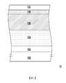
圖1是依照本發明之第一實施例的一種半導體磊晶結構的剖面示意圖。FIG. 1 is a schematic cross-sectional view of a semiconductor epitaxial structure according to a first embodiment of the invention.
圖2是依照本發明之第二實施例的一種半導體磊晶結構的剖面示意圖。2 is a schematic cross-sectional view of a semiconductor epitaxial structure according to a second embodiment of the invention.
參照本實施例之圖式以更全面地闡述本發明。然而,本發明亦可以各種不同的形式體現,而不應限於本文中之實施例。圖式中的層與區域的厚度會為了清楚起見而放大。相同或相似之標號表示相同或相似之元件,以下段落將不再一一贅述。The present invention is explained more fully with reference to the drawings of this embodiment. However, the present invention can also be embodied in various forms and should not be limited to the embodiments herein. The thickness of the layers and regions in the drawing will be exaggerated for clarity. The same or similar reference numerals indicate the same or similar elements, and the following paragraphs will not repeat them one by one.
圖1是依照本發明之第一實施例的一種半導體磊晶結構的剖面示意圖。以下實施例之半導體磊晶結構可應用於場效電晶體領域,例如高功率場效電晶體(high power field-effect transistors)、高頻電晶體(high efficiency transistors)或高電子遷移率電晶體(high electron mobility transistors,HEMT)等。FIG. 1 is a schematic cross-sectional view of a semiconductor epitaxial structure according to a first embodiment of the invention. The semiconductor epitaxial structure of the following embodiments can be applied to the field of field-effect transistors, such as high power field-effect transistors, high-efficiency transistors, or high-electron mobility transistors ( high electron mobility transistors, HEMT) etc.
請參照圖1,本發明之第一實施例的半導體磊晶結構10由下到上依序包括:基板100、成核層102、緩衝層104、半導體層106、阻障層108以及頂蓋層110。半導體磊晶結構10的形成方法如下所示。1, the semiconductor
首先,提供基板100。在一實施例中,基板100可視為一成長基板,其材料可例如是藍寶石(Sapphire)、碳化矽(SiC)、氮化鋁(AlN)、矽(Si)、鍺(Ge)、砷化鎵(GaAs)、磷化銦(InP)、磷化鎵(GaP)、氮化鎵(GaN)或其組合。在本實施例中,基板100可以是矽基板,其晶面(crystal plane)可例如但不限於是(111)、(110)、(100)等。在其他實施例中,基板100亦可以是絕緣體上矽(silicon-on-insulator,SOI)基板。First, the
接著,於基板100上選擇性地形成成核層102。在一實施例中,成核層102可包括AlN層、Al層或其組合。成核層102的形成方法可例如是金屬有機化學氣相沉積法(metal organic chemical vapor deposition,MOCVD)或分子束磊晶法(molecular beam epitaxy,MBE),其厚度可介於0nm至50nm之間。在一些實施例中,成核層102可防止基板100的Si與後續形成的緩衝層104或半導體層106的Ga反應而形成共熔金屬的回熔現象。在替代實施例中,成核層102可降低基板100與後續形成的緩衝層104之間的缺陷密度,以減少應力。Next, a
之後,於成核層102上形成緩衝層104,使得成核層102位於基板100與緩衝層104之間。在一實施例中,緩衝層104可以是超晶格結構(superlattice structure)以及/或漸變結構(graded structure)。超晶格結構可包括至少兩個不同的疊層結構(laminated structure),舉例來說,緩衝層104由下到上依序包括第一疊層、第二疊層以及第三疊層。第一疊層包括交替堆疊的多個AlN層與多個AlxGa1-xN層;第二疊層包括交替堆疊的多個AlN層與多個AlyGa1-yN層;而第三疊層包括交替堆疊的多個AlN層與多個AlzGa1-zN層,其中x>y>z。也就是說,緩衝層104中的Al含量是從成核層102朝向後續形成的半導體層106的方向減少。另一方面,漸變結構是指在整個緩衝層104中具有濃度變化的層,舉例來說,緩衝層104包括多個AlN層與多個AlxGa1-xN層,X值可從成核層102朝向後續形成的半導體層106的方向漸變,於此,所謂漸變可以是步階漸變(step grading)、連續漸變、不連續漸變或其組合。After that, a
值得注意的是,由於緩衝層104可舒緩基板100(或成核層102)與半導體層106之間由於晶格常數所導致的應力累積。因此,本實施例的緩衝層104可減少半導體層106與基板100之間因熱膨脹係數差異而產生的應力,以避免裂紋或破片。另外,最靠近成核層102的緩衝層104的Al含量高於最靠近半導體層106的緩衝層104的Al含量,其可提升磊晶品質且有利於後續元件開發。It is worth noting that the
在一些實施例中,緩衝層104的形成方法可以是金屬有機化學氣相沉積法(MOCVD)或分子束磊晶法(MBE),其厚度可介於750nm至1800nm之間。在其他實施例中,緩衝層104的材料包括多個AlN層與多個AlGaN層所構成的疊層結構、多個AlN層與多個GaN層所構成的疊層結構、多個GaN層與多個AlGaN層所構成的疊層結構等。In some embodiments, the method for forming the
接著,於緩衝層104上形成半導體層106,使得緩衝層104位於成核層102與半導體層106之間。在一實施例中,半導體層106可以是氮化物半導體層,例如是未經摻雜(undoped)或非刻意摻雜(unintentionally doped)氮化鎵(GaN)層、碳摻雜GaN層、鐵摻雜GaN層或其組合。在替代實施例中,半導體層106的形成方法可例如是金屬有機化學氣相沉積法(MOCVD)或分子束磊晶法(MBE),其厚度可介於515nm至1500nm之間。Next, a
在其他實施例中,半導體層106可包括底層與配置於所述底層上的通道層。具有高電子遷移率的二維電子氣(2-dimensional electron gas,2DEG)可形成於所述通道層中,以形成高電子遷移率電晶體(HEMT)。In other embodiments, the
然後,於半導體層106上形成阻障層108,使得半導體層106位於緩衝層104與阻障層108之間。在一實施例中,阻障層108的材料包括AlGaN、AlN、AlInN、InN、AlGnInN或其組合。在一些實施例中,阻障層108的形成方法可以是金屬有機化學氣相沉積法(MOCVD)或分子束磊晶法(MBE),其厚度可介於4nm至30nm之間。Then, a
接著,於阻障層108上形成頂蓋層110,使得阻障層108位於半導體層106與頂蓋層110之間。在一實施例中,頂蓋層110的材料包括GaN、Si3N4或其組合。在一些實施例中,阻障層108的形成方法可以是金屬有機化學氣相沉積法(MOCVD)、分子束磊晶法(MBE)或電漿增強化學氣相沉積法(PECVD),其厚度可介於2nm至4nm之間。Next, a
值得注意的是,在本實施例中,在半導體磊晶結構10的曲率小於等於+/-100km-1以及/或翹曲率小於等於+/-30微米的情況下,半導體層106的厚度與緩衝層104的厚度的比值的最大值或最小值以下列式子表示:Y=aX1-bX2+cX3,X1≧0nm,X2≧750nm,X3≧515nm,其中X1為成核層102的厚度,X2為緩衝層104的厚度,X3為半導體層106的厚度,a、b、c分別為常數,Y為半導體層106的厚度與緩衝層104的厚度的比值(X3/X2)並且介於所述最大值與所述最小值之間。於此,所謂的「曲率(curvature)」是指磊晶製程期間的半導體磊晶結構的彎曲程度,此時的半導體磊晶結構的溫度可介於700℃至1200℃之間。另外,所謂的「翹曲率(bowing)」是指室溫下半導體磊晶結構的彎曲程度,其中室溫可介於20℃至30℃之間。It is worth noting that in this embodiment, when the curvature of the
一般而言,當半導體磊晶結構的曲率大於+/-100km-1時,其降至室溫後的翹曲率則會大於+/-30微米,此結果稱之為塑性變形(plastic deformation)。所謂「塑性變形」是指材料受外力作用而形變時,若過了一定的限度便不能恢復原狀,此變形稱之為塑性變形。也就是說,當半導體磊晶結構的曲率大於+/-100km-1時,即使降至室溫,半導體磊晶結構的翹曲率仍無法恢復原狀。因此,本發明實施例可使半導體磊晶結構的翹曲率小於等於+/-100km-1,以使降至室溫後的半導體磊晶結構的曲率小於等於+/-30微米,進而避免塑性變形的產生,並提升半導體磊晶結構的良率。Generally speaking, when the curvature of the semiconductor epitaxial structure is greater than +/-100km-1 , the curvature after it is lowered to room temperature will be greater than +/-30 microns. This result is called plastic deformation. The so-called "plastic deformation" means that when a material is deformed by an external force, it cannot be restored to its original shape after a certain limit. This deformation is called plastic deformation. That is to say, when the curvature of the semiconductor epitaxial structure is greater than +/-100km-1 , even if it is lowered to room temperature, the curvature of the semiconductor epitaxial structure cannot be restored to its original state. Therefore, in the embodiment of the present invention, the curvature of the semiconductor epitaxial structure can be less than or equal to +/-100km-1 , so that the curvature of the semiconductor epitaxial structure after being lowered to room temperature is less than or equal to +/-30 microns, thereby avoiding plastic deformation And improve the yield of semiconductor epitaxial structures.
在一些實施例中,當a為0.098167,b為0.008583,且c為0.005652時,藉由上述式子可求得半導體層106的厚度與緩衝層104的厚度的比值的最大值。也就是說,先設定成核層102的厚度,並將成核層102的預設厚度(例如X1=0nm、10nm、20nm或36nm)與緩衝層104的最小厚度(例如X2=750nm)代入下列式(1):Y=0.098167×X1-0.008583×X2+0.005652×X3 (1)In some embodiments, when a is 0.098167, b is 0.008583, and c is 0.005652, the maximum value of the ratio of the thickness of the
在此情況下,便可求得在半導體磊晶結構10的曲率小於等於+/-100km-1以及/或翹曲率小於等於+/-30微米的情況下,當成核層102為預設厚度時,半導體層106的厚度與緩衝層104的厚度的比值的最大值,也就是半導體層106的厚度除以緩衝層104的厚度的比值的最大值。In this case, it can be obtained that when the curvature of the
為了證明本發明的可實現性,以下列舉多個實例來對本發明之半導體磊晶結構10做更進一步地說明。雖然描述了以下實驗,但是在不逾越本發明範疇的情況下,可適當改變所用材料、其量及比率、處理細節以及處理流程等等。因此,不應根據下文所述的實驗對本發明作出限制性的解釋。In order to prove the feasibility of the present invention, a number of examples are listed below to further illustrate the

實例1-實例4Example 1-Example 4
提供矽基板。接著,藉由MOCVD在矽基板上依序形成成核層(AlN層)、緩衝層(多個AlN層與AlGaN層交替堆疊所形成的超晶格結構)以及半導體層(未摻雜及有摻雜之GaN層)。成核層的厚度、緩衝層的厚度以及半導體層的厚度如表1所示。然後,量測實例1-實例4的半導體磊晶結構的彎曲程度,實例1-實例4的半導體磊晶結構的曲率皆小於等於+/-100km-1以及/或翹曲率皆小於等於+/-30微米。Provide silicon substrate. Next, a nucleation layer (AlN layer), a buffer layer (a superlattice structure formed by alternately stacking multiple AlN layers and AlGaN layers), and a semiconductor layer (undoped and doped) are sequentially formed on the silicon substrate by MOCVD. Hybrid GaN layer). The thickness of the nucleation layer, the thickness of the buffer layer and the thickness of the semiconductor layer are shown in Table 1. Then, the degree of curvature of the semiconductor epitaxial structure of Example 1 to Example 4 was measured. The curvature of the semiconductor epitaxial structure of Example 1 to Example 4 was all less than or equal to +/-100km-1 and/or the curvature was less than or equal to +/- 30 microns.
由表1可知,將實例1-實例4所量測出來成核層的厚度X1、緩衝層的厚度X2以及半導體層的厚度X3是滿足上述式(1)。也就是說,上述等式(1)中等號的左右兩邊是相等的。因此,本發明實施例可設定不同成核層的厚度,並藉由上述式(1)求得半導體層的厚度與緩衝層的厚度的比值Y的最大值。It can be seen from Table 1 that the thickness X1 of the nucleation layer, the thickness X2 of the buffer layer, and the thickness X3 of the semiconductor layer measured in Examples 1 to 4 satisfy the above formula (1). In other words, the left and right sides of the equal sign in the above equation (1) are equal. Therefore, in the embodiment of the present invention, the thickness of different nucleation layers can be set, and the maximum value of the ratio Y of the thickness of the semiconductor layer to the thickness of the buffer layer can be obtained by the above formula (1).
在另一實施例中,當a為0.09546,b為-0.003735,且c為-0.012168時,藉由上述式子則可求得半導體層106的厚度與緩衝層104的厚度的比值的最小值。也就是說,先設定成核層102的厚度,並將成核層102的預設厚度(例如X1=0nm、10nm、20nm或36nm)與半導體層106的最小厚度(例如X3=515nm)代入下列式(2):Y=0.09546×X1+0.003735×X2-0.012168×X3 (2)In another embodiment, when a is 0.09546, b is -0.003735, and c is -0.012168, the minimum value of the ratio of the thickness of the
在此情況下,便可求得在半導體磊晶結構10的曲率小於等於+/-100km-1以及/或翹曲率小於等於+/-30微米的情況下,當成核層102為預設厚度時,半導體層106的厚度與緩衝層104的厚度的比值的最小值,也就是半導體層106的厚度除以緩衝層104的厚度的比值的最小值。In this case, it can be obtained that when the curvature of the

實例5-實例8Example 5-Example 8
實例5-8的形成步驟類似上述實例1-4的形成步驟,其中成核層的厚度、緩衝層的厚度以及半導體層的厚度如表2所示。然後,量測實例5-實例8的半導體磊晶結構的彎曲程度,實例5-實例8的半導體磊晶結構的曲率皆小於等於+/-100km-1以及/或翹曲率皆小於等於+/-30微米。The formation steps of Examples 5-8 are similar to those of the above-mentioned Examples 1-4, wherein the thickness of the nucleation layer, the thickness of the buffer layer, and the thickness of the semiconductor layer are shown in Table 2. Then, the degree of curvature of the semiconductor epitaxial structure of Example 5 to Example 8 is measured, and the curvature of the semiconductor epitaxial structure of Example 5 to Example 8 is all less than or equal to +/-100km-1 and/or the curvature is less than or equal to +/- 30 microns.
由表2可知,將實例5-實例8所量測出來成核層的厚度X1、緩衝層的厚度X2以及半導體層的厚度X3是滿足上述式(2)。也就是說,上述等式(2)中等號的左右兩邊是相等或相似的。因此,本發明實施例可設定不同成核層的厚度,並藉由上述式(2)求得半導體層的厚度與緩衝層的厚度的比值Y的最小值。It can be seen from Table 2 that the thickness X1 of the nucleation layer, the thickness X2 of the buffer layer, and the thickness X3 of the semiconductor layer measured in Example 5 to Example 8 satisfy the above formula (2). In other words, the left and right sides of the equal sign in the above equation (2) are equal or similar. Therefore, in the embodiment of the present invention, the thickness of different nucleation layers can be set, and the minimum value of the ratio Y of the thickness of the semiconductor layer to the thickness of the buffer layer can be obtained by the above formula (2).
另外,由表1與表2可知,當成核層的厚度為0nm至36nm時,緩衝層的厚度可介於750nm至1755nm之間,而半導體層的厚度可介於515nm至1491nm之間。此外,半導體層的厚度與緩衝層的厚度的比值Y的最大值可介於0.89至1.99之間,且最小值可介於0.29至0.56之間。換言之,在上述厚度範圍區間或比值Y區間內,半導體磊晶結構的曲率可小於等於+/-100km-1以及/或翹曲率可小於等於+/-30微米,以減少滑移線、裂紋,更甚至破片等缺陷的產生,進而提升半導體磊晶結構的良率。In addition, as can be seen from Table 1 and Table 2, when the thickness of the nucleation layer is 0 nm to 36 nm, the thickness of the buffer layer can be between 750 nm and 1755 nm, and the thickness of the semiconductor layer can be between 515 nm and 1491 nm. In addition, the maximum value of the ratio Y of the thickness of the semiconductor layer to the thickness of the buffer layer may be between 0.89 and 1.99, and the minimum value may be between 0.29 and 0.56. In other words, in the above thickness range or ratio Y range, the curvature of the semiconductor epitaxial structure can be less than or equal to +/-100km-1 and/or the warpage can be less than or equal to +/-30 microns to reduce slip lines and cracks. Even the occurrence of defects such as fragments, which in turn improves the yield of semiconductor epitaxial structures.
圖2是依照本發明之第二實施例的一種半導體磊晶結構的剖面示意圖。2 is a schematic cross-sectional view of a semiconductor epitaxial structure according to a second embodiment of the invention.
請參照圖2,基本上,第二實施例的半導體磊晶結構20與第一實施例的半導體磊晶結構10相似。上述兩者不同之處在於:第二實施例之半導體磊晶結構20還包括間隔層107位於半導體層106與阻障層108之間。在一實施例中,間隔層107可包括AlN層。在一些實施例中,間隔層107的形成方法可例如是金屬有機化學氣相沉積法(MOCVD)或分子束磊晶法(MBE),其厚度可介於1nm至2nm之間。在另一實施例中,間隔層107的材料與阻障層108的材料不同,且間隔層107的晶格常數可小於阻障層108的晶格常數。在替代實施例中,間隔層107可增加電子遷移率並增加載子侷限能力,進而改善2DEG特性。2, basically, the
值得注意的是,在本實施例中,在半導體磊晶結構20的曲率小於等於+/-100km-1以及/或翹曲率小於等於+/-30微米的情況下,半導體層106的厚度與緩衝層104的厚度的比值的最大值或最小值以下列式子表示:Y=aX1-bX2+cX3,X1≧0nm,X2≧750nm,X3≧515nm,其中X1為成核層102的厚度,X2為緩衝層104的厚度,X3為半導體層106的厚度,a、b、c分別為常數,Y為半導體層106的厚度與緩衝層104的厚度的比值(X3/X2)並且介於所述最大值與所述最小值之間。It is worth noting that in this embodiment, when the curvature of the
舉例來說,在一些實施例中,當a為0.10249,b為0.006845,且c為0.00583時,藉由上述式子可求得半導體層106的厚度與緩衝層104的厚度的比值的最大值。也就是說,先設定成核層102的厚度,並將成核層102的預設厚度(例如X1=0nm、10nm、20nm或21nm)與緩衝層104的最小厚度(例如X2=750nm)代入下列式(3):Y=0.10249×X1-0.006845×X2+0.00583×X3 (3)For example, in some embodiments, when a is 0.10249, b is 0.006845, and c is 0.00583, the maximum value of the ratio of the thickness of the
在此情況下,便可求得在半導體磊晶結構20的曲率小於等於+/-100km-1以及/或翹曲率小於等於+/-30微米的情況下,當成核層102為預設厚度時,半導體層106的厚度與緩衝層104的厚度的比值的最大值。In this case, it can be obtained that when the curvature of the
為了證明本發明的可實現性,以下列舉多個實例來對本發明之半導體磊晶結構20做更進一步地說明。In order to prove the feasibility of the present invention, a number of examples are listed below to further illustrate the

實例9-實例12Example 9-Example 12
提供矽基板。接著,藉由MOCVD在矽基板上依序形成成核層(AlN層)、緩衝層(多個AlN層與AlGaN層交替堆疊所形成的超晶格結構)、半導體層(未摻雜及有摻雜之GaN層)以及間隔層(AlN層)。成核層的厚度、緩衝層的厚度以及半導體層的厚度如表3所示,而間隔層的厚度則約為1nm。然後,量測實例9-實例12的半導體磊晶結構的彎曲程度,實例9-實例12的半導體磊晶結構的曲率皆小於等於+/-100km-1以及/或翹曲率皆小於等於+/-30微米。Provide silicon substrate. Then, a nucleation layer (AlN layer), a buffer layer (a superlattice structure formed by alternately stacking multiple AlN layers and AlGaN layers), a semiconductor layer (undoped and doped) are sequentially formed on the silicon substrate by MOCVD. Hybrid GaN layer) and spacer layer (AlN layer). The thickness of the nucleation layer, the thickness of the buffer layer, and the thickness of the semiconductor layer are shown in Table 3, and the thickness of the spacer layer is about 1 nm. Then, the degree of curvature of the semiconductor epitaxial structure of Example 9 to Example 12 is measured, and the curvature of the semiconductor epitaxial structure of Example 9 to Example 12 is all less than or equal to +/-100km-1 and/or the curvature is less than or equal to +/- 30 microns.
由表3可知,將實例9-實例12所量測出來成核層的厚度X1、緩衝層的厚度X2以及半導體層的厚度X3是滿足上述式(3)。也就是說,上述等式(3)中等號的左右兩邊是相等或相似的。因此,本發明實施例可設定不同成核層的厚度,並藉由上述式(3)求得半導體層的厚度與緩衝層的厚度的比值Y的最大值。It can be seen from Table 3 that the thickness X1 of the nucleation layer, the thickness X2 of the buffer layer, and the thickness X3 of the semiconductor layer measured in Example 9 to Example 12 satisfy the above formula (3). In other words, the left and right sides of the equal sign in the above equation (3) are equal or similar. Therefore, in the embodiment of the present invention, the thickness of different nucleation layers can be set, and half of the thickness can be obtained by the above formula (3).The maximum value of the ratio Y of the thickness of the conductor layer to the thickness of the buffer layer.
在另一實施例中,當a為-0.6908,b為0.030257,且c為0.08209時,藉由上述式子則可求得半導體層106的厚度與緩衝層104的厚度的比值的最小值。也就是說,先設定成核層102的厚度,並將成核層102的預設厚度(例如X1=0nm、10nm、20nm或21nm)與半導體層106的最小厚度(例如X3=515nm)代入下列式(4):Y=-0.6908×X1-0.030257×X2+0.08209×X3 (4)In another embodiment, when a is -0.6908, b is 0.030257, and c is 0.08209, the minimum value of the ratio of the thickness of the
在此情況下,便可求得在半導體磊晶結構20的曲率小於等於+/-100km-1以及/或翹曲率小於等於+/-30微米的情況下,當成核層102為預設厚度時,半導體層106的厚度與緩衝層104的厚度的比值的最小值。In this case, it can be obtained that when the curvature of the

實例13-實例16Example 13-Example 16
實例13-16的形成步驟類似上述實例9-12的形成步驟,其中成核層的厚度、緩衝層的厚度以及半導體層的厚度如表4所示,而間隔層的厚度則約為1nm。然後,量測實例13-實例16的半導體磊晶結構的彎曲程度,實例13-實例16的半導體磊晶結構的曲率皆小於等於+/-100km-1以及/或翹曲率皆小於等於+/-30微米。The formation steps of Examples 13-16 are similar to those of Examples 9-12, wherein the thickness of the nucleation layer, the thickness of the buffer layer, and the thickness of the semiconductor layer are shown in Table 4, and the thickness of the spacer layer is about 1 nm. Then, the degree of curvature of the semiconductor epitaxial structure of Example 13 to Example 16 was measured, and the curvature of the semiconductor epitaxial structure of Example 13 to Example 16 was all less than or equal to +/-100km-1 and/or the curvature was less than or equal to +/- 30 microns.
由表4可知,將實例13-實例16所量測出來成核層的厚度X1、緩衝層的厚度X2以及半導體層的厚度X3是滿足上述式(4)。也就是說,上述等式(4)中等號的左右兩邊是相等的。因此,本發明實施例可設定不同成核層的厚度,並藉由上述式(4)求得半導體層的厚度與緩衝層的厚度的比值Y的最小值。It can be seen from Table 4 that the thickness X1 of the nucleation layer, the thickness X2 of the buffer layer, and the thickness X3 of the semiconductor layer measured in Example 13 to Example 16 satisfy the above formula (4). In other words, the left and right sides of the equal sign in the above equation (4) are equal. Therefore, in the embodiment of the present invention, the thickness of different nucleation layers can be set, and the minimum value of the ratio Y of the thickness of the semiconductor layer to the thickness of the buffer layer can be obtained by the above formula (4).
由表3與表4可知,當成核層的厚度為0nm至21nm時,緩衝層的厚度可介於750nm至1385nm之間,半導體層的厚度可介於515nm至1141nm之間。此外,半導體層的厚度與緩衝層的厚度的比值Y的最大值可介於0.88至1.52之間,且最小值可介於0.37至0.57之間。換言之,在上述厚度範圍區間或比值Y區間內,半導體磊晶結構的曲率可小於等於+/-100km-1以及/或翹曲率可小於等於+/-30微米,以減少滑移線、裂紋,更甚至破片等缺陷的產生,進而提升半導體磊晶結構的良率。It can be seen from Table 3 and Table 4 that when the thickness of the nucleation layer is 0 nm to 21 nm, the thickness of the buffer layer can be between 750 nm and 1385 nm, and the thickness of the semiconductor layer can be between 515 nm and 1141 nm. In addition, the maximum value of the ratio Y of the thickness of the semiconductor layer to the thickness of the buffer layer may be between 0.88 and 1.52, and the minimum value may be between 0.37 and 0.57. In other words, in the above thickness range or ratio Y range, the curvature of the semiconductor epitaxial structure can be less than or equal to +/-100km-1 and/or the warpage can be less than or equal to +/-30 microns to reduce slip lines and cracks. Even the occurrence of defects such as fragments, which in turn improves the yield of semiconductor epitaxial structures.
綜上所述,本發明實施例可設定不同成核層的厚度,並藉由上述式子求得半導體層的厚度與緩衝層的厚度的比值的最大值或最小值,以使半導體磊晶結構的翹曲率或曲率小於等於預定值,進而減少滑移線、裂紋,更甚至破片等缺陷的產生,並提升半導體磊晶結構的良率。In summary, the embodiment of the present invention can set the thickness of different nucleation layers, and obtain the maximum or minimum ratio of the thickness of the semiconductor layer to the thickness of the buffer layer by the above formula, so as to make the semiconductor epitaxial structure The warpage or curvature is less than or equal to a predetermined value, thereby reducing the occurrence of defects such as slip lines, cracks, and even fragments, and improving the yield of semiconductor epitaxial structures.
雖然本發明已以實施例揭露如上,然其並非用以限定本發明,任何所屬技術領域中具有通常知識者,在不脫離本發明的精神和範圍內,當可作些許的更動與潤飾,故本發明的保護範圍當視後附的申請專利範圍所界定者為準。Although the present invention has been disclosed in the above embodiments, it is not intended to limit the present invention. Anyone with ordinary knowledge in the technical field can make slight changes and modifications without departing from the spirit and scope of the present invention. The scope of protection of the present invention shall be subject to those defined by the attached patent scope.
10:半導體磊晶結構10: Semiconductor epitaxial structure
100:基板100: substrate
102:成核層102: Nucleation layer
104:緩衝層104: buffer layer
106:半導體層106: semiconductor layer
108:阻障層108: barrier layer
110:頂蓋層110: top cover
Claims (10)
Translated fromChinesePriority Applications (3)
| Application Number | Priority Date | Filing Date | Title |
|---|---|---|---|
| TW108125591ATWI698914B (en) | 2019-07-19 | 2019-07-19 | Semiconductor epitaxial structure and method of forming the same |
| CN202010567762.5ACN112242435B (en) | 2019-07-19 | 2020-06-19 | Semiconductor epitaxial structure and method for forming the same |
| US16/920,318US20210017669A1 (en) | 2019-07-19 | 2020-07-02 | Semiconductor epitaxial structure and method of forming the same |
Applications Claiming Priority (1)
| Application Number | Priority Date | Filing Date | Title |
|---|---|---|---|
| TW108125591ATWI698914B (en) | 2019-07-19 | 2019-07-19 | Semiconductor epitaxial structure and method of forming the same |
Publications (2)
| Publication Number | Publication Date |
|---|---|
| TWI698914Btrue TWI698914B (en) | 2020-07-11 |
| TW202105473A TW202105473A (en) | 2021-02-01 |
Family
ID=72601767
Family Applications (1)
| Application Number | Title | Priority Date | Filing Date |
|---|---|---|---|
| TW108125591ATWI698914B (en) | 2019-07-19 | 2019-07-19 | Semiconductor epitaxial structure and method of forming the same |
Country Status (3)
| Country | Link |
|---|---|
| US (1) | US20210017669A1 (en) |
| CN (1) | CN112242435B (en) |
| TW (1) | TWI698914B (en) |
Families Citing this family (5)
| Publication number | Priority date | Publication date | Assignee | Title |
|---|---|---|---|---|
| TWI683370B (en)* | 2019-03-12 | 2020-01-21 | 環球晶圓股份有限公司 | Semiconductor device and manufacturng method thereof |
| TWI790655B (en)* | 2021-06-21 | 2023-01-21 | 世界先進積體電路股份有限公司 | Semiconductor structure and high electron mobility transistor |
| US11967642B2 (en) | 2021-09-03 | 2024-04-23 | Vanguard International Semiconductor Corporation | Semiconductor structure, high electron mobility transistor and fabrication method thereof |
| TWI838935B (en)* | 2022-08-18 | 2024-04-11 | 環球晶圓股份有限公司 | Light-emitting element structure |
| TWI866625B (en)* | 2023-11-20 | 2024-12-11 | 英屬開曼群島商海珀電子股份有限公司 | High electron mobility transistor |
Citations (1)
| Publication number | Priority date | Publication date | Assignee | Title |
|---|---|---|---|---|
| TW201839807A (en)* | 2017-04-28 | 2018-11-01 | 環球晶圓股份有限公司 | Composite Substrate for Epitaxy and Method of Making the Same |
Family Cites Families (14)
| Publication number | Priority date | Publication date | Assignee | Title |
|---|---|---|---|---|
| US7198671B2 (en)* | 2001-07-11 | 2007-04-03 | Matsushita Electric Industrial Co., Ltd. | Layered substrates for epitaxial processing, and device |
| US7976630B2 (en)* | 2008-09-11 | 2011-07-12 | Soraa, Inc. | Large-area seed for ammonothermal growth of bulk gallium nitride and method of manufacture |
| JP5491116B2 (en)* | 2009-09-25 | 2014-05-14 | 日本碍子株式会社 | Epitaxial substrate for semiconductor element, semiconductor element, and manufacturing method of epitaxial substrate for semiconductor element |
| US8785305B2 (en)* | 2009-12-11 | 2014-07-22 | National Semiconductor Corporation | Backside stress compensation for gallium nitride or other nitride-based semiconductor devices |
| GB2485418B (en)* | 2010-11-15 | 2014-10-01 | Dandan Zhu | Semiconductor materials |
| US10529820B2 (en)* | 2014-07-15 | 2020-01-07 | Bae Systems Information And Electronic Systems Integration Inc. | Method for gallium nitride on diamond semiconductor wafer production |
| US9337023B1 (en)* | 2014-12-15 | 2016-05-10 | Texas Instruments Incorporated | Buffer stack for group IIIA-N devices |
| US20160380045A1 (en)* | 2015-06-25 | 2016-12-29 | Tivra Corporation | Crystalline semiconductor growth on amorphous and poly-crystalline substrates |
| WO2016209282A1 (en)* | 2015-06-26 | 2016-12-29 | Intel Corporation | Gan devices on engineered silicon substrates |
| US20190288089A9 (en)* | 2015-12-28 | 2019-09-19 | Texas Instruments Incorporated | Methods for transistor epitaxial stack fabrication |
| US10347591B2 (en)* | 2016-09-16 | 2019-07-09 | Ii-Vi Delaware, Inc. | Metallic, tunable thin film stress compensation for epitaxial wafers |
| RU169283U1 (en)* | 2016-11-15 | 2017-03-14 | Федеральное государственное бюджетное учреждение науки Научно-технологический центр микроэлектроники и субмикронных гетероструктур Российской академии наук | Heterostructure field transistor InGaAIN / SiC |
| EP3451364B1 (en)* | 2017-08-28 | 2020-02-26 | Siltronic AG | Heteroepitaxial wafer and method for producing a heteroepitaxial wafer |
| US11183563B2 (en)* | 2019-10-04 | 2021-11-23 | Vanguard International Semiconductor Corporation | Substrate structure and method for fabricating semiconductor structure including the substrate structure |
- 2019
- 2019-07-19TWTW108125591Apatent/TWI698914B/enactive
- 2020
- 2020-06-19CNCN202010567762.5Apatent/CN112242435B/enactiveActive
- 2020-07-02USUS16/920,318patent/US20210017669A1/ennot_activeAbandoned
Patent Citations (1)
| Publication number | Priority date | Publication date | Assignee | Title |
|---|---|---|---|---|
| TW201839807A (en)* | 2017-04-28 | 2018-11-01 | 環球晶圓股份有限公司 | Composite Substrate for Epitaxy and Method of Making the Same |
Also Published As
| Publication number | Publication date |
|---|---|
| CN112242435B (en) | 2024-06-11 |
| CN112242435A (en) | 2021-01-19 |
| TW202105473A (en) | 2021-02-01 |
| US20210017669A1 (en) | 2021-01-21 |
Similar Documents
| Publication | Publication Date | Title |
|---|---|---|
| TWI698914B (en) | Semiconductor epitaxial structure and method of forming the same | |
| JP5836158B2 (en) | III-nitride semiconductor structure with strain absorbing interlayer transition module | |
| CN103515419B (en) | The gradient aluminium gallium nitride alloy and super-lattice buffer layer of III V group iii nitride layers on silicon substrate | |
| CN102859695A (en) | Epitaxial substrate and method for producing epitaxial substrate | |
| JP5133927B2 (en) | Compound semiconductor substrate | |
| CN104054166A (en) | Epitaxial Wafers for Heterojunction Field Effect Transistors | |
| US11114555B2 (en) | High electron mobility transistor device and methods for forming the same | |
| JP2003059948A (en) | Semiconductor device and production method therefor | |
| CN102484049A (en) | Epitaxial Substrate For Semiconductor Element, Method For Manufacturing Epitaxial Substrate For Semiconductor Element, And Semiconductor Element | |
| CN104126223A (en) | Semiconductor element and method for manufacturing semiconductor element | |
| TWI683372B (en) | Semiconductor device and method of forming the same | |
| JP6141627B2 (en) | Method for forming GaN layer on silicon substrate and GaN substrate | |
| EP2581929A1 (en) | Epitaxial substrate and method for producing epitaxial substrate | |
| CN104885198A (en) | Group-iii nitride epitaxial substrate and method for producing same | |
| JP5824814B2 (en) | Semiconductor wafer, semiconductor element, and manufacturing method thereof | |
| TWI713221B (en) | High electron mobility transistor and methods for forming the same | |
| TW202140866A (en) | Epitaxial structure with super-lattice laminate | |
| CN113539786A (en) | Silicon-based gallium nitride epitaxial structure and preparation method thereof | |
| JP2015103665A (en) | Nitride semiconductor epitaxial wafer and nitride semiconductor | |
| CN111146282B (en) | High electron mobility transistor device and method of manufacturing the same | |
| JP6205497B2 (en) | Manufacturing method of nitride semiconductor | |
| US10629718B2 (en) | III-nitride epitaxial structure | |
| US9401420B2 (en) | Semiconductor device | |
| CN106449375A (en) | Semiconductor device with silicon-doped aluminum nitride layer and production method thereof | |
| CN111146269A (en) | High electron mobility transistor device and method of manufacturing the same |