TWI695543B - Antenna module and inspection method of antenna module - Google Patents
Antenna module and inspection method of antenna moduleDownload PDFInfo
- Publication number
- TWI695543B TWI695543BTW107133425ATW107133425ATWI695543BTW I695543 BTWI695543 BTW I695543BTW 107133425 ATW107133425 ATW 107133425ATW 107133425 ATW107133425 ATW 107133425ATW I695543 BTWI695543 BTW I695543B
- Authority
- TW
- Taiwan
- Prior art keywords
- antenna
- power supply
- supply line
- circuit
- inspection
- Prior art date
Links
- 238000007689inspectionMethods0.000titleclaimsabstractdescription176
- 238000000034methodMethods0.000titleclaimsdescription22
- 230000005855radiationEffects0.000claimsabstractdescription60
- 238000012545processingMethods0.000claimsabstractdescription34
- 238000001514detection methodMethods0.000claimsdescription26
- 239000010410layerSubstances0.000claimsdescription25
- 238000004891communicationMethods0.000claimsdescription24
- 230000005540biological transmissionEffects0.000claimsdescription11
- 239000000758substrateSubstances0.000claimsdescription8
- 239000011241protective layerSubstances0.000claimsdescription7
- 230000001939inductive effectEffects0.000claimsdescription4
- 230000008054signal transmissionEffects0.000claimsdescription3
- 230000002159abnormal effectEffects0.000claimsdescription2
- 238000012986modificationMethods0.000description40
- 230000004048modificationEffects0.000description40
- 238000003860storageMethods0.000description16
- 238000010586diagramMethods0.000description14
- 229920005989resinPolymers0.000description9
- 239000011347resinSubstances0.000description9
- 230000005856abnormalityEffects0.000description4
- 239000004020conductorSubstances0.000description4
- 230000005611electricityEffects0.000description4
- 239000007769metal materialSubstances0.000description4
- 239000000523sampleSubstances0.000description4
- 238000007789sealingMethods0.000description4
- 230000003068static effectEffects0.000description4
- 229920000106Liquid crystal polymerPolymers0.000description3
- 239000004977Liquid-crystal polymers (LCPs)Substances0.000description3
- 239000000919ceramicSubstances0.000description3
- 239000000470constituentSubstances0.000description3
- 230000006870functionEffects0.000description3
- 230000002950deficientEffects0.000description2
- 238000009826distributionMethods0.000description2
- 239000011159matrix materialSubstances0.000description2
- 229910000679solderInorganic materials0.000description2
- RYGMFSIKBFXOCR-UHFFFAOYSA-NCopperChemical compound[Cu]RYGMFSIKBFXOCR-UHFFFAOYSA-N0.000description1
- 239000004593EpoxySubstances0.000description1
- YCKRFDGAMUMZLT-UHFFFAOYSA-NFluorine atomChemical compound[F]YCKRFDGAMUMZLT-UHFFFAOYSA-N0.000description1
- 101000760620Homo sapiens Cell adhesion molecule 1Proteins0.000description1
- 101001139126Homo sapiens Krueppel-like factor 6Proteins0.000description1
- 101000661816Homo sapiens Suppression of tumorigenicity 18 proteinProteins0.000description1
- 239000004642PolyimideSubstances0.000description1
- BQCADISMDOOEFD-UHFFFAOYSA-NSilverChemical compound[Ag]BQCADISMDOOEFD-UHFFFAOYSA-N0.000description1
- 239000000956alloySubstances0.000description1
- 229910010293ceramic materialInorganic materials0.000description1
- 239000011247coating layerSubstances0.000description1
- 229910052802copperInorganic materials0.000description1
- 239000010949copperSubstances0.000description1
- 229910052731fluorineInorganic materials0.000description1
- 239000011737fluorineSubstances0.000description1
- PCHJSUWPFVWCPO-UHFFFAOYSA-NgoldChemical compound[Au]PCHJSUWPFVWCPO-UHFFFAOYSA-N0.000description1
- 229910052737goldInorganic materials0.000description1
- 239000010931goldSubstances0.000description1
- 238000010030laminatingMethods0.000description1
- 238000004519manufacturing processMethods0.000description1
- 239000000463materialSubstances0.000description1
- 230000000149penetrating effectEffects0.000description1
- 229920001721polyimidePolymers0.000description1
- 229910052709silverInorganic materials0.000description1
- 239000004332silverSubstances0.000description1
- 238000012360testing methodMethods0.000description1
Images


Classifications
- H—ELECTRICITY
- H01—ELECTRIC ELEMENTS
- H01Q—ANTENNAS, i.e. RADIO AERIALS
- H01Q1/00—Details of, or arrangements associated with, antennas
- H01Q1/12—Supports; Mounting means
- H01Q1/22—Supports; Mounting means by structural association with other equipment or articles
- H01Q1/2283—Supports; Mounting means by structural association with other equipment or articles mounted in or on the surface of a semiconductor substrate as a chip-type antenna or integrated with other components into an IC package
- G—PHYSICS
- G01—MEASURING; TESTING
- G01R—MEASURING ELECTRIC VARIABLES; MEASURING MAGNETIC VARIABLES
- G01R31/00—Arrangements for testing electric properties; Arrangements for locating electric faults; Arrangements for electrical testing characterised by what is being tested not provided for elsewhere
- G01R31/50—Testing of electric apparatus, lines, cables or components for short-circuits, continuity, leakage current or incorrect line connections
- G01R31/54—Testing for continuity
- H—ELECTRICITY
- H01—ELECTRIC ELEMENTS
- H01Q—ANTENNAS, i.e. RADIO AERIALS
- H01Q1/00—Details of, or arrangements associated with, antennas
- H01Q1/36—Structural form of radiating elements, e.g. cone, spiral, umbrella; Particular materials used therewith
- H01Q1/38—Structural form of radiating elements, e.g. cone, spiral, umbrella; Particular materials used therewith formed by a conductive layer on an insulating support
- H—ELECTRICITY
- H01—ELECTRIC ELEMENTS
- H01Q—ANTENNAS, i.e. RADIO AERIALS
- H01Q1/00—Details of, or arrangements associated with, antennas
- H01Q1/48—Earthing means; Earth screens; Counterpoises
- H—ELECTRICITY
- H01—ELECTRIC ELEMENTS
- H01Q—ANTENNAS, i.e. RADIO AERIALS
- H01Q21/00—Antenna arrays or systems
- H01Q21/06—Arrays of individually energised antenna units similarly polarised and spaced apart
- H01Q21/061—Two dimensional planar arrays
- H01Q21/065—Patch antenna array
- H—ELECTRICITY
- H01—ELECTRIC ELEMENTS
- H01Q—ANTENNAS, i.e. RADIO AERIALS
- H01Q3/00—Arrangements for changing or varying the orientation or the shape of the directional pattern of the waves radiated from an antenna or antenna system
- H01Q3/26—Arrangements for changing or varying the orientation or the shape of the directional pattern of the waves radiated from an antenna or antenna system varying the relative phase or relative amplitude of energisation between two or more active radiating elements; varying the distribution of energy across a radiating aperture
- H01Q3/267—Phased-array testing or checking devices
- H—ELECTRICITY
- H01—ELECTRIC ELEMENTS
- H01Q—ANTENNAS, i.e. RADIO AERIALS
- H01Q5/00—Arrangements for simultaneous operation of antennas on two or more different wavebands, e.g. dual-band or multi-band arrangements
- H01Q5/30—Arrangements for providing operation on different wavebands
- H01Q5/378—Combination of fed elements with parasitic elements
- H—ELECTRICITY
- H01—ELECTRIC ELEMENTS
- H01Q—ANTENNAS, i.e. RADIO AERIALS
- H01Q9/00—Electrically-short antennas having dimensions not more than twice the operating wavelength and consisting of conductive active radiating elements
- H01Q9/04—Resonant antennas
- H01Q9/0407—Substantially flat resonant element parallel to ground plane, e.g. patch antenna
- H01Q9/0414—Substantially flat resonant element parallel to ground plane, e.g. patch antenna in a stacked or folded configuration
- H—ELECTRICITY
- H01—ELECTRIC ELEMENTS
- H01Q—ANTENNAS, i.e. RADIO AERIALS
- H01Q9/00—Electrically-short antennas having dimensions not more than twice the operating wavelength and consisting of conductive active radiating elements
- H01Q9/04—Resonant antennas
- H01Q9/0407—Substantially flat resonant element parallel to ground plane, e.g. patch antenna
- H01Q9/0428—Substantially flat resonant element parallel to ground plane, e.g. patch antenna radiating a circular polarised wave
- H01Q9/0435—Substantially flat resonant element parallel to ground plane, e.g. patch antenna radiating a circular polarised wave using two feed points
- H—ELECTRICITY
- H01—ELECTRIC ELEMENTS
- H01L—SEMICONDUCTOR DEVICES NOT COVERED BY CLASS H10
- H01L2223/00—Details relating to semiconductor or other solid state devices covered by the group H01L23/00
- H01L2223/58—Structural electrical arrangements for semiconductor devices not otherwise provided for
- H01L2223/64—Impedance arrangements
- H01L2223/66—High-frequency adaptations
- H01L2223/6661—High-frequency adaptations for passive devices
- H01L2223/6677—High-frequency adaptations for passive devices for antenna, e.g. antenna included within housing of semiconductor device
- H—ELECTRICITY
- H01—ELECTRIC ELEMENTS
- H01L—SEMICONDUCTOR DEVICES NOT COVERED BY CLASS H10
- H01L2224/00—Indexing scheme for arrangements for connecting or disconnecting semiconductor or solid-state bodies and methods related thereto as covered by H01L24/00
- H01L2224/01—Means for bonding being attached to, or being formed on, the surface to be connected, e.g. chip-to-package, die-attach, "first-level" interconnects; Manufacturing methods related thereto
- H01L2224/10—Bump connectors; Manufacturing methods related thereto
- H01L2224/15—Structure, shape, material or disposition of the bump connectors after the connecting process
- H01L2224/16—Structure, shape, material or disposition of the bump connectors after the connecting process of an individual bump connector
- H01L2224/161—Disposition
- H01L2224/16151—Disposition the bump connector connecting between a semiconductor or solid-state body and an item not being a semiconductor or solid-state body, e.g. chip-to-substrate, chip-to-passive
- H01L2224/16221—Disposition the bump connector connecting between a semiconductor or solid-state body and an item not being a semiconductor or solid-state body, e.g. chip-to-substrate, chip-to-passive the body and the item being stacked
- H01L2224/16225—Disposition the bump connector connecting between a semiconductor or solid-state body and an item not being a semiconductor or solid-state body, e.g. chip-to-substrate, chip-to-passive the body and the item being stacked the item being non-metallic, e.g. insulating substrate with or without metallisation
- H01L2224/16227—Disposition the bump connector connecting between a semiconductor or solid-state body and an item not being a semiconductor or solid-state body, e.g. chip-to-substrate, chip-to-passive the body and the item being stacked the item being non-metallic, e.g. insulating substrate with or without metallisation the bump connector connecting to a bond pad of the item
- H—ELECTRICITY
- H01—ELECTRIC ELEMENTS
- H01L—SEMICONDUCTOR DEVICES NOT COVERED BY CLASS H10
- H01L2924/00—Indexing scheme for arrangements or methods for connecting or disconnecting semiconductor or solid-state bodies as covered by H01L24/00
- H01L2924/15—Details of package parts other than the semiconductor or other solid state devices to be connected
- H01L2924/151—Die mounting substrate
- H01L2924/1517—Multilayer substrate
- H01L2924/15192—Resurf arrangement of the internal vias
- H—ELECTRICITY
- H01—ELECTRIC ELEMENTS
- H01L—SEMICONDUCTOR DEVICES NOT COVERED BY CLASS H10
- H01L2924/00—Indexing scheme for arrangements or methods for connecting or disconnecting semiconductor or solid-state bodies as covered by H01L24/00
- H01L2924/15—Details of package parts other than the semiconductor or other solid state devices to be connected
- H01L2924/151—Die mounting substrate
- H01L2924/153—Connection portion
- H01L2924/1531—Connection portion the connection portion being formed only on the surface of the substrate opposite to the die mounting surface
- H01L2924/15311—Connection portion the connection portion being formed only on the surface of the substrate opposite to the die mounting surface being a ball array, e.g. BGA
- H—ELECTRICITY
- H01—ELECTRIC ELEMENTS
- H01L—SEMICONDUCTOR DEVICES NOT COVERED BY CLASS H10
- H01L2924/00—Indexing scheme for arrangements or methods for connecting or disconnecting semiconductor or solid-state bodies as covered by H01L24/00
- H01L2924/15—Details of package parts other than the semiconductor or other solid state devices to be connected
- H01L2924/151—Die mounting substrate
- H01L2924/153—Connection portion
- H01L2924/1531—Connection portion the connection portion being formed only on the surface of the substrate opposite to the die mounting surface
- H01L2924/15313—Connection portion the connection portion being formed only on the surface of the substrate opposite to the die mounting surface being a land array, e.g. LGA
Landscapes
- Engineering & Computer Science (AREA)
- Microelectronics & Electronic Packaging (AREA)
- Physics & Mathematics (AREA)
- General Physics & Mathematics (AREA)
- Variable-Direction Aerials And Aerial Arrays (AREA)
- Waveguide Aerials (AREA)
Abstract
Translated fromChineseDescription
Translated fromChinese本發明係關於一種天線模組及天線模組的檢查方法。The invention relates to an antenna module and an inspection method of the antenna module.
專利文獻1中,記載有具備天線構件之通訊裝置與通訊裝置之檢查方法。專利文獻1之通訊裝置具備天線導體、以及與天線導體連接之天線端子。天線導體係由被覆層所覆蓋。另外,天線端子係未由被覆層所覆蓋之導通檢查用之端子。專利文獻1之通訊裝置係使探針接觸天線端子及接地端子而進行導通檢查,來作為通訊裝置之檢查。
現有技術文獻Existing technical literature
專利文獻Patent Literature
專利文獻1:日本專利特開2014-11746號公報Patent Document 1: Japanese Patent Laid-Open No. 2014-11746
專利文獻1之導通檢查方法中,必須使探針接觸各天線端子,例如於進行多個通訊裝置之檢查之情形時、或包含多個天線導體之通訊裝置中,存在無法容易地進行導通檢查之可能性。In the continuity inspection method of
本發明之目的在於提供一種可容易進行導通檢查之天線模組及天線模組的檢查方法。An object of the present invention is to provide an antenna module and an antenna module inspection method that can easily perform continuity inspection.
本發明之一形態之天線模組,具備:基體;天線,其具有設置於上述基體之放射元件;第1供電線路及第2供電線路,其與上述放射元件連接;以及控制電路,其經由上述第1供電線路及上述第2供電線路而與上述放射元件連接;上述控制電路包含:訊號處理電路,其經由上述第1供電線路或上述第2供電線路而與上述天線連接;以及天線檢查電路,其對連接有上述第1供電線路、上述放射元件、及上述第2供電線路之導通路徑之導通進行檢查。An antenna module according to an aspect of the present invention includes: a base; an antenna having a radiating element provided on the base; a first power supply line and a second power supply line connected to the radiating element; and a control circuit via the above The first power supply line and the second power supply line are connected to the radiation element; the control circuit includes: a signal processing circuit connected to the antenna via the first power supply line or the second power supply line; and an antenna inspection circuit, It checks the conduction of the conduction path to which the first power supply line, the radiation element, and the second power supply line are connected.
依據本發明之天線模組及天線模組的檢查方法,可容易進行導通檢查。According to the antenna module and the inspection method of the antenna module of the present invention, continuity inspection can be easily performed.
1、1A-1L‧‧‧天線模組1. 1A-1L‧‧‧ Antenna module
2‧‧‧基帶模組2‧‧‧ Baseband module
4‧‧‧檢查裝置4‧‧‧ Inspection device
10‧‧‧基體10‧‧‧Matrix
10a‧‧‧第1面10a‧‧‧The first side
10b‧‧‧第2面10b‧‧‧The second side
11‧‧‧密封樹脂11‧‧‧Sealing resin
12‧‧‧保護層12‧‧‧Protective layer
13‧‧‧屏蔽構件13‧‧‧Shielding member
14、14A‧‧‧電路基板14, 14A‧‧‧ circuit board
15‧‧‧訊號路徑15‧‧‧Signal path
16‧‧‧連接端子16‧‧‧Connecting terminal
20‧‧‧天線20‧‧‧ Antenna
20-1‧‧‧第1天線20-1‧‧‧1st antenna
20-2‧‧‧第2天線20-2‧‧‧ 2nd antenna
20-3‧‧‧第3天線20-3‧‧‧ Third antenna
20-4‧‧‧第4天線20-4‧‧‧ 4th antenna
20-5‧‧‧第5天線20-5‧‧‧ 5th antenna
20-6‧‧‧第6天線20-6‧‧‧The sixth antenna
21‧‧‧放射元件21‧‧‧Radiation element
22‧‧‧無供電元件22‧‧‧No power supply components
23‧‧‧第1埠23‧‧‧
24‧‧‧第2埠24‧‧‧
25‧‧‧第3埠25‧‧‧ Port 3
26‧‧‧第4埠26‧‧‧
27‧‧‧通路27‧‧‧ access
28‧‧‧襯墊28‧‧‧Padding
29‧‧‧配線29‧‧‧Wiring
30‧‧‧控制電路30‧‧‧Control circuit
31‧‧‧連接端子31‧‧‧Connecting terminal
33‧‧‧第1供電線路33‧‧‧First power supply line
34‧‧‧第2供電線路34‧‧‧The second power supply line
35‧‧‧第3供電線路35‧‧‧The third power supply line
36‧‧‧第4供電線路36‧‧‧The fourth power supply line
41‧‧‧控制部41‧‧‧Control Department
42‧‧‧儲存部42‧‧‧Storage Department
43‧‧‧輸入部43‧‧‧ Input
50‧‧‧訊號處理電路50‧‧‧Signal processing circuit
51‧‧‧發送電路51‧‧‧Sending circuit
52‧‧‧接收電路52‧‧‧Receiving circuit
60‧‧‧天線檢查電路60‧‧‧ Antenna inspection circuit
61‧‧‧檢查控制電路61‧‧‧Check control circuit
62‧‧‧電源端子62‧‧‧Power terminal
63‧‧‧儲存電路63‧‧‧Storage circuit
64‧‧‧連接切換電路64‧‧‧Connect switching circuit
65‧‧‧檢測電路65‧‧‧ detection circuit
66‧‧‧判定電路66‧‧‧Judgment circuit
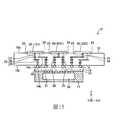
圖1係第1實施形態之天線模組之俯視圖。FIG. 1 is a plan view of the antenna module of the first embodiment.
圖2係沿著圖1之II-II'線之剖面圖。FIG. 2 is a cross-sectional view taken along line II-II' of FIG. 1. FIG.
圖3係沿著圖2之III-III'線之剖面圖。FIG. 3 is a cross-sectional view taken along line III-III' of FIG. 2.
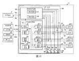
圖4係表示第1實施形態之天線模組之構成例的方塊圖。4 is a block diagram showing a configuration example of the antenna module of the first embodiment.
圖5係示意性表示輸出訊號、與天線之導通狀態之關係的圖表。FIG. 5 is a graph schematically showing the relationship between the output signal and the conduction state of the antenna.
圖6係表示第1實施形態之天線模組之導通檢查方法的流程圖。FIG. 6 is a flowchart showing the continuity checking method of the antenna module according to the first embodiment.
圖7係表示第1實施形態之天線模組之導通檢查方法之其他例的流程圖。FIG. 7 is a flowchart showing another example of the continuity inspection method of the antenna module according to the first embodiment.
圖8係表示第1實施形態之變形例之天線模組之構成例的方塊圖。8 is a block diagram showing a configuration example of an antenna module according to a modification of the first embodiment.
圖9係表示第2實施形態之天線模組之放射元件的俯視圖。9 is a plan view showing the radiation element of the antenna module of the second embodiment.
圖10係表示第2實施形態之天線模組之構成例的方塊圖。FIG. 10 is a block diagram showing an example of the configuration of the antenna module of the second embodiment.
圖11係表示第2實施形態之天線模組之導通檢查方法的流程圖。FIG. 11 is a flowchart showing the continuity checking method of the antenna module of the second embodiment.
圖12係表示第3實施形態之天線模組的剖面圖。12 is a cross-sectional view showing an antenna module of a third embodiment.
圖13係表示第3實施形態之第1變形例之天線模組的剖面圖。13 is a cross-sectional view showing an antenna module according to a first modification of the third embodiment.
圖14係表示第3實施形態之第2變形例之天線模組的剖面圖。14 is a cross-sectional view showing an antenna module according to a second modification of the third embodiment.
圖15係表示第3實施形態之第3變形例之天線模組的剖面圖。15 is a cross-sectional view showing an antenna module according to a third modification of the third embodiment.
圖16係表示第3實施形態之第4變形例之天線模組的剖面圖。16 is a cross-sectional view showing an antenna module according to a fourth modification of the third embodiment.
圖17係表示第4實施形態之天線模組之構成例的方塊圖。FIG. 17 is a block diagram showing a configuration example of an antenna module according to the fourth embodiment.
圖18係表示第4實施形態之第1變形例之天線模組之構成例的方塊圖。18 is a block diagram showing a configuration example of an antenna module according to a first modification of the fourth embodiment.
圖19係表示第4實施形態之第2變形例之天線模組之構成例的方塊圖。19 is a block diagram showing a configuration example of an antenna module according to a second modification of the fourth embodiment.
圖20係表示第4實施形態之第3變形例之天線模組之構成例的方塊圖。20 is a block diagram showing a configuration example of an antenna module according to a third modification of the fourth embodiment.
圖21係表示第5實施形態之天線模組之剖面圖。21 is a cross-sectional view showing an antenna module of a fifth embodiment.
參照圖式,對用以實施本發明之實施形態進行詳細說明。並非藉由以下之實施形態中記載之內容來限定本發明。另外,以下記載之構成要素中包含本技術領域中具有通常知識者可容易設想者、實質上相同者、所謂均等之範圍者。進而,以下記載之構成要素可適當組合。另外,亦存在一部分之構成要素未使用之情形。With reference to the drawings, embodiments of the present invention will be described in detail. The present invention is not limited by the contents described in the following embodiments. In addition, the constituent elements described below include those that can be easily assumed by those having ordinary knowledge in the technical field, those that are substantially the same, and so-called equal ranges. Furthermore, the constituent elements described below can be combined as appropriate. In addition, some of the constituent elements are not used.
(第1實施形態)(First embodiment)
圖1係第1實施形態之天線模組之俯視圖。圖2係沿著圖1之II-II'線之剖面圖。圖3係沿著圖2之III-III'線之剖面圖。如圖1所示,本實施形態之天線模組1包含:基體10、複數個第1天線20-1、第2天線20-2、第3天線20-3、第4天線20-4、第5天線20-5及第6天線20-6。此外,以下之說明中,於無需將第1天線20-1、第2天線20-2、第3天線20-3、第4天線20-4、第5天線20-5、第6天線20-6加以區別來說明之情形時,表示為天線20。天線20分別具備放射元件21(未圖 示)、及無供電元件22。FIG. 1 is a plan view of the antenna module of the first embodiment. FIG. 2 is a cross-sectional view taken along line II-II' of FIG. 1. FIG. FIG. 3 is a cross-sectional view taken along line III-III' of FIG. 2. As shown in FIG. 1, the
以下之說明中,將與基體10之第1面10a平行之面內之一方向設為X方向。另外,在與第1面10a平行之面內將與X方向正交之方向設為Y方向。另外,將與X方向及Y方向分別正交之方向設為Z方向。此外,並不限定於此,Y方向亦可相對於X方向而以90°以外之角度交叉。Z方向亦可相對於X方向及Y方向而以90°以外之角度交叉。In the following description, one direction in the plane parallel to the
如圖1所示,複數個天線20配置為行列狀。即,天線20於X方向排列複數個,且於Y方向排列複數個。天線模組1為包含複數個天線20之陣列天線。As shown in FIG. 1, a plurality of
如圖2所示,天線模組1更包含控制電路30、第1供電線路33、及第2供電線路34。基體10包含第1面10a、以及與第1面10a相反側之第2面10b。基體10係使用例如低溫共燒陶瓷多層基板(LTCC(Low Temperature Co-fired Ceramics)多層基板)。基體10具有於Z方向積層之複數個絕緣層。各絕緣層係使用可於1000℃以下之低溫下進行煅燒之陶瓷材料,形成為薄層狀。此外,並不限定於此,基體10亦可為將包含環氧、聚醯亞胺等樹脂之樹脂層積層複數層而形成之多層樹脂基板。另外,亦可使用具有更低之介電常數之液晶聚合物(Liquid Crystal Polymer:LCP)或者氟系樹脂而形成基體10。或者,基體10亦可為陶瓷多層基板。基體10可為具有可撓性之可撓性基板,亦可為具有熱塑性之剛性基板。As shown in FIG. 2, the
天線20係例如以WiGig(Wireless Gigabit)來使用之60GHz頻帶之高頻訊號中使用之貼片天線。天線20分別具備放射元件21、及無供電元件22。放射元件21設置於基體10之內層。無供電元件22係與放射元件21對向而設置於基體10之第1面10a上。無供電元件22係經由基體10之絕緣層而與放射元件21重疊配置。即,無供電元件22係與放射元件21絕緣之狀態。放射元件21及無 供電元件22係使用銅、銀、金、或者包含該等之合金材料等具有導電性之金屬材料而形成。The
如圖1所示,無供電元件22係於X方向排列複數個,且於Y方向排列複數個。另外,如圖3所示,亦與放射元件21同樣,於X方向排列複數個,且於Y方向排列複數個。如圖1及圖3所示,放射元件21與無供電元件22均於俯視時為四角形狀,為同一形狀。此外,放射元件21及無供電元件22並不限定於四角形狀,亦可為圓形狀、多角形狀等其他形狀。另外,放射元件21與無供電元件22亦可具有相互不同之形狀。As shown in FIG. 1, the
如圖2所示,於放射元件21上,連接第1供電線路33之一端及第2供電線路34之一端。第1供電線路33之另一端及第2供電線路34之另一端係經由連接端子31而與控制電路30連接。As shown in FIG. 2, one end of the first
第1供電線路33及第2供電線路34分別包含通路27、襯墊28及配線29。通路27形成為於Z方向貫通基體10之各絕緣層之柱狀導體。具體而言,通路27於貫通絕緣層之貫通孔之內部設置有具有導電性之金屬材料。襯墊28設置於絕緣層之間,將於Z方向相鄰之通路27彼此連接,或者將通路27與配線29連接。配線29設置於基體10之內層,將俯視時不同位置之複數個通路27連接。通路27、襯墊28及配線29係與放射元件21同樣,使用具有導電性之金屬材料。The first
第1供電線路33之與放射元件21連接之部分為第1埠23。另外,第2供電線路34之與放射元件21連接之部分為第2埠24。如圖3所示,第1埠23配置於從天線20之中心21c起於Y方向偏移之位置。此處,放射元件21具有於X方向對向之2個邊21s1、21s2以及邊21s1與邊21s2之間之2個邊21s3、21s4。中心21c係與如下交點一致,即,將邊21s1之中點與邊21s2之中點連結之虛擬線、與將邊21s3之中點與邊21s4之中點連結之虛擬線之交點。第1埠23配置於放射元件21之沿著X方向之邊21s4之近旁。另外,第2埠24配置於從天線20之中心21c起 於X方向偏移之位置。第2埠24配置於放射元件21之沿著Y方向之邊21s2之近旁。The portion of the first
如圖2所示,控制電路30係經由連接端子31而構裝於基體10之第2面10b上。連接端子31例如為焊球凸塊。控制電路30係由密封樹脂11所密封。控制電路30係不僅控制經由天線20之訊號之收發,而且控制第1供電線路33、天線20之放射元件21及第2供電線路34之導通檢查的電路。控制電路30例如為RFIC(Radio Frequency Integrated Circuit,射頻積體電路)。As shown in FIG. 2, the
藉由如上所述之構成,天線模組1之控制電路30與各天線20電性連接。具體而言,天線模組1之第1供電線路33、天線20之放射元件21、及第2供電線路34係經由連接端子31而與控制電路30連接。藉此,天線模組1的連接有第1供電線路33、天線20之放射元件21、及第2供電線路34之導通路徑成為閉環電路。With the above-mentioned structure, the
若控制電路30之訊號處理電路50(參照圖4)對第1埠23供給高頻訊號,則於放射元件21中,於Y方向流通電流。藉由於Y方向流通之電流,而放射出與Y方向平行之極化波。另外,若控制電路30之訊號處理電路50對第2埠24供給高頻訊號,則於放射元件21中,於X方向流通電流。藉由於X方向流通之電流,而放射出與X方向平行之極化波。藉此,可藉由對第1埠23、第2埠24之任一者供給高頻訊號,來切換天線20之極化波。If the
放射元件21若被激發,則與無供電元件22進行電磁耦合。於該情形時,天線20具有共振頻率不同之2個共振模式。因此,與省略無供電元件22之情形相比較,可實現天線20之寬頻帶化。另外,複數個天線20構成陣列天線,藉由控制天線20之放射元件21之配置、或所激發之高頻訊號之振幅、相位,而獲得所需之放射圖案(指向性)。When the
繼而,對控制電路30之構成進行說明。圖4係表示第1實施形態 之天線模組之構成例的方塊圖。圖5係示意性表示輸出訊號、與天線之導通狀態之關係的圖表。此外,圖4中,對天線模組1包含n個天線20之例進行說明。即,如圖4所示,天線模組1包含第1天線(ANT1)20-1、第2天線(ANT2)20-2、......、第n-1天線(ANTn-1)20-(n-1)、第n天線(ANTn)20-n。Next, the configuration of the
如圖4所示,控制電路30包含訊號處理電路50、及天線檢查電路60。訊號處理電路50係經由第1供電線路33及第2供電線路34而與天線20連接。訊號處理電路50係經由天線20而有助於訊號之收發。天線檢查電路60係對包含第1供電線路33、天線20之放射元件21(參照圖2)及第2供電線路34之導通路徑之導通進行檢查之電路。控制電路30可將通訊模式、及檢查模式進行切換而實行。通訊模式中,控制電路30係根據來自外部之控制訊號,藉由訊號處理電路50之動作,經由天線20來進行訊號之收發。檢查模式中,控制電路30係藉由天線檢查電路60之動作來檢查天線20之導通。As shown in FIG. 4, the
天線檢查電路60係經由第1連接配線L1、L2,而分別與第1供電線路33、第2供電線路34電性連接。於第1連接配線L1、L2上,第2連接配線L11、L12分支而分別連接。訊號處理電路50係經由第2連接配線L11、L12而與第1供電線路33、第2供電線路34電性連接。即,各天線20係與訊號處理電路50以及天線檢查電路60電性連接。The
訊號處理電路50包含發送電路51及接收電路52。於發送時,基帶模組2將基帶訊號Va供給至發送電路51。發送電路51將基帶訊號Va調變為高頻訊號(例如60GHz)。而且,發送電路51經由第1供電線路33及第2供電線路34而將高頻訊號供給至各天線20。另外,於接收時,來自各天線20之高頻訊號供給至接收電路52。接收電路52將所接收之高頻訊號解調為基帶訊號Vb,且將基帶訊號Vb供給至基帶模組2。此外,接收電路52亦可輸出具有較基帶訊號Vb高之頻率之中間頻率訊號。The
與控制電路30連接之外部之檢查裝置4例如為試驗機、資料記錄器、個人電腦等。檢查裝置4具備控制部41、儲存部42、及輸入部43。控制部41為例如以CPU(Central Processing Unit,中央處理單元)等構成之運算處理裝置。儲存部42係儲存用於控制導通檢查之軟體程式、或各天線20之導通檢查結果等各種資訊。儲存部42係作為例如快閃記憶體(Flash Memory)等不揮發性之儲存裝置而發揮功能之電路。輸入部43為例如鍵盤或觸控面板等輸入裝置。操作者從輸入部43來輸入與導通檢查有關之資訊。本實施形態中,天線模組1包含天線檢查電路60。因此,可使外部之檢查裝置4之構成簡易。另外,即使於天線20之數量不同之情形時,亦可利用通用之檢查裝置4來進行導通檢查。The
天線檢查電路60包含:檢查控制電路61、電源端子62、儲存電路63、複數個檢測電路65-1、65-2、......、65-(n-1)、65-n、及判定電路66。此外,以下之說明中,於無需將檢測電路65-1、65-2、......、65-(n-1)、65-n加以區別而說明之情形時,表示為檢測電路65。The
檢查控制電路61係對電源端子62、儲存電路63、複數個檢測電路65以及判定電路66之動作進行控制之控制電路。檢查控制電路61係根據來自檢查裝置4之控制訊號Vc、檢查開始訊號Vst,來控制導通檢查。檢查控制電路61進而根據控制訊號Vc,而對訊號處理電路50輸出控制訊號Vd。訊號處理電路50根據控制訊號Vd而停止動作,於進行導通檢查時停止對天線20之供電及訊號之輸入輸出。The
電源端子62將導通檢查用之輸入訊號Vin經由檢測電路65而供給至各天線20。The
檢測電路65-1、65-2、......、65-(n-1)、65-n分別經由第1連接配線L1、L2,而與第1天線20-1、第2天線20-2、......、第n-1天線20-(n- 1)、第n天線20-n電性連接。檢測電路65係對來自第1供電線路33、天線20及第2供電線路34之輸出訊號Vout進行檢測之電路。檢測電路65係將連接第1供電線路33之連接端子31、與連接第2供電線路34之連接端子31之間的端子間電壓作為輸出訊號Vout而進行檢測。檢測電路65將輸出訊號Vout輸出至判定電路66。此外,並不限定於此,檢測電路65亦可採用對第1供電線路33、天線20及第2供電線路34中所流通之電流進行檢測之構成。The detection circuits 65-1, 65-2, ..., 65-(n-1), 65-n are connected to the first antenna 20-1 and the second antenna via the first connection wiring L1, L2, respectively 20-2, ..., n-1 antenna 20-(n-1), n-th antenna 20-n are electrically connected. The
判定電路66係根據輸出訊號Vout,來判定第1供電線路33、天線20之放射元件21及第2供電線路34之導通的電路。判定電路66為包含例如比較器之電路。判定電路66對每個天線20,將與導通狀態對應之檢查訊號Adet作為數位訊號而供給至儲存電路63。判定電路66於天線20之導通良好之情形時,輸出「1」而作為檢查訊號Adet,於天線20之導通不良之情形時,輸出「0」而作為檢查訊號Adet。The
圖5中示出判定電路66之判定方法之一例。判定電路66將輸出訊號Vout與基準訊號Vref1、Vref2進行比較。基準訊號Vref1、Vref2係根據儲存於檢查裝置4之儲存部42之基準值的電壓訊號。An example of the determination method of the
判定電路66於輸出訊號Vout為基準訊號Vref1以上、基準訊號Vref2以下之情形時,判定為由第1供電線路33、天線20之放射元件21及第2供電線路34所形成之閉環電路之導通良好(OK)。於該情形時,判定電路66輸出「1」而作為檢查訊號Adet。另一方面,判定電路66於輸出訊號Vout小於基準訊號Vref1之情形時,判定為由第1供電線路33、天線20之放射元件21及第2供電線路34所形成之閉環電路之一部分短路(SHORT)。另外,判定電路66於輸出訊號Vout大於基準訊號Vref2之情形時,判定為由第1供電線路33、天線20之放射元件21及第2供電線路34所形成之閉環電路之一部分斷路(OPEN)。判定電路66於判定為短路(SHORT)或者斷路(OPEN)之情形時,輸出「0」而作為檢 查訊號Adet。The
儲存電路63係對每個天線20保持檢查訊號Adet之電路。檢查控制電路61於導通檢查結束之情形時,將檢查訊號Adet輸出至檢查裝置4。藉此,可檢查天線20之導通。此外,圖4中所示之天線檢查電路60之構成僅為一例,可適當變更。例如,儲存電路63等天線檢查電路60之一部分之功能亦可包含於外部之檢查裝置4中。The
如上所述,本實施形態之天線模組1可使用經由天線20之訊號之收發中所使用之第1供電線路33及第2供電線路34,來進行設置於基體10之內層之放射元件21之導通檢查。假設於第1供電線路33及第2供電線路34分別設置有導通檢查用之端子或配線等之情形時,於60GHz頻帶之毫米波之收發中,存在天線20之性能變化之可能性。本實施形態中,由於無需設置導通檢查用之端子或配線等,故而可抑制天線20之性能之變化。As described above, the
繼而,參照圖4至圖6,對天線模組1之導通檢查方法進行說明。圖6係表示第1實施形態之天線模組之導通檢查方法的流程圖。如圖6所示,控制電路30判定檢查開始訊號Vst是否輸入(步驟ST1)。於檢查開始訊號Vst未輸入之情形時(步驟ST1,否),控制電路30判定通訊控制訊號是否輸入(步驟ST8)。通訊控制訊號係對經由天線之訊號之收發功能進行控制之訊號,例如由未圖示之控制基板所供給。於通訊控制訊號輸入之情形時(步驟ST8,是),控制電路30實行通訊模式(步驟ST9)。藉此,訊號處理電路50係經由天線20而進行訊號之收發。於通訊控制訊號未輸入之情形時(步驟ST8,否),控制電路30不實行通訊模式,亦不實行檢查模式,返回至步驟ST1。Next, referring to FIG. 4 to FIG. 6, the continuity inspection method of the
於檢查開始訊號Vst輸入之情形時(步驟ST1,是),控制電路30實行檢查模式(步驟ST2)。檢查控制電路61將檢查開始訊號Vst作為觸發器,使電源端子62、儲存電路63、複數個檢測電路65以及判定電路66開始動 作。首先,檢查控制電路61實行第1天線20-1之導通檢查(步驟ST3)。藉由電源端子62、檢測電路65-1、判定電路66之動作,與第1天線20-1之導通狀態對應之檢查訊號Adet保持於儲存電路63中。若第1天線20-1之導通檢查結束,則檢查控制電路61實行第2天線20-2之導通檢查(步驟ST4)。同樣,檢查控制電路61依序實行各天線20之導通檢查,實行第(n-1)天線20-(n-1)之導通檢查(步驟ST5),且實行第n天線20-n之導通檢查(步驟ST6)。When the check start signal Vst is input (step ST1, YES), the
如此,檢查控制電路61對複數個天線20依序檢查導通。而且,經檢查之所有天線20之檢查訊號Adet保持於儲存電路63中。若對於所有天線20,檢查結束,則檢查控制電路61將檢查結果輸出至檢查裝置4(步驟ST7)。本實施形態中,供給至檢查裝置4之檢查結果為所有天線20之每一個之檢查訊號Adet。藉此,可確定複數個天線20中的產生導通異常之天線20。In this way, the
圖6所示之導通檢查方法僅為一例,可適當變更。圖7係表示第1實施形態之天線模組之導通檢查方法之其他例的流程圖。如圖7所示,將通訊模式與檢查模式進行切換而實行之方法(步驟ST11、ST12、ST17、ST18)係與圖6所示之例相同。The continuity check method shown in FIG. 6 is only an example and can be changed as appropriate. FIG. 7 is a flowchart showing another example of the continuity inspection method of the antenna module according to the first embodiment. As shown in FIG. 7, the method (steps ST11, ST12, ST17, ST18) performed by switching the communication mode and the inspection mode is the same as the example shown in FIG. 6.
檢查控制電路61將檢查開始訊號Vst作為觸發器,首先,實行第1天線20-1之導通檢查(步驟ST13-1)。判定電路66判斷第1天線20-1之導通是否良好(步驟ST13-2)。於第1天線20-1之導通不良(短路或者斷路)之情形時(步驟ST13-2,否),檢查控制電路61係根據來自判定電路66之檢查訊號Adet,結束導通檢查,將檢查結果輸出至檢查裝置4(步驟ST16)。該情形時之檢查結果係表示天線模組1中產生導通不良。The
於第1天線20-1之導通良好之情形時(步驟ST13-2,是),檢查控制電路61實行第2天線20-2之導通檢查(步驟ST14-1)。判定電路66判斷第2天線20-2之導通是否良好(步驟ST14-2)。於第2天線20-2之導通不良(短路或 者斷路)之情形時(步驟ST14-2,否),檢查控制電路61結束導通檢查,將檢查結果輸出至檢查裝置4(步驟ST16)。於第2天線20-2之導通良好之情形時(步驟ST14-2,是),同樣依序實行天線20之導通檢查。When the continuity of the first antenna 20-1 is good (step ST13-2, YES), the
檢查控制電路61實行第n天線20-n之導通檢查(步驟ST15-1)。判定電路66判斷第n天線20-n之導通是否良好(步驟ST15-2)。於第n天線20-n之導通不良(短路或者斷路)之情形時(步驟ST15-2,否),檢查控制電路61結束導通檢查,將檢查結果輸出至檢查裝置4(步驟ST16)。於第n天線20-n之導通良好之情形時(步驟ST15-2,是),檢查控制電路61結束導通檢查,將表示所有天線20之導通良好之檢查結果輸出至檢查裝置4(步驟ST16)。The
如上所述,本申請案實施例中之其他例中,若於複數個天線20中之任一個天線20中檢測出導通不良,則判斷為天線模組1中產生導通不良,結束導通檢查。因此,由於在即使發現一個不良天線20之時間點結束檢查,故而與對所有之天線20進行檢查後加以判斷之方法相比,可於短時間內進行導通檢查。另外,由於無需保持個別之天線20之檢查訊號Adet,故而可縮小儲存電路63之規模。As described above, in other examples of the embodiments of the present application, if any of the plurality of
(變形例)(Modification)
圖8係表示第1實施形態之變形例之天線模組之構成例的方塊圖。本實施形態之天線模組1A中,天線檢查電路60更包含連接切換電路64。另外,檢測電路65僅設置有一個。連接切換電路64係根據來自檢查控制電路61之控制訊號,而將檢測電路65、與各天線20之連接進行切換之開關電路。8 is a block diagram showing a configuration example of an antenna module according to a modification of the first embodiment. In the
檢查模式中,檢查控制電路61藉由連接切換電路64之動作,而將檢測電路65、與第1天線20-1連接,實行第1天線20-1之導通檢查。繼而,檢查控制電路61藉由連接切換電路64之動作,將檢測電路65、與第2天線20-2連接,實行第2天線20-2之導通檢查。如此一來,連接切換電路64將檢測電路65、 與各天線20分時而依序連接。藉此,天線模組1A可以與圖6所示之導通檢查方法相同之方式,實行所有天線20之導通檢查。In the inspection mode, the
本變形例中,由於設置有連接切換電路64,故而無需對每個天線20設置檢測電路65。因此,於天線20之數量多之情形時,可縮小天線檢查電路60之電路規模。In this modification, since the
如以上所說明,本實施形態之天線模組1、1A具備:基體10;天線20,其具有設置於基體10之內層之放射元件21;第1供電線路33及第2供電線路34,其與放射元件21連接;以及控制電路30,其經由第1供電線路33及第2供電線路34而與放射元件21連接。控制電路30包含:訊號處理電路50,其經由第1供電線路33或第2供電線路34而與天線20連接;以及天線檢查電路60,其對包含第1供電線路33、放射元件21及第2供電線路34之導通路徑之導通進行檢查。As described above, the
藉此,可使用經由天線20之訊號收發中所使用之第1供電線路33及第2供電線路34,來進行設置於基體10之內層之放射元件21之導通檢查。另外,由於無需設置導通檢查用之端子或配線等,故而可抑制經由天線20之訊號之收發性能變化。另外,由於控制電路30包含對各天線20之導通進行檢查之天線檢查電路60,故而可使探針不接觸各天線20,而容易地進行導通檢查。As a result, the first
本實施形態之天線模組1、1A中,控制電路30將以下模式進行切換而實行:通訊模式,其藉由訊號處理電路50之動作,經由天線20而進行訊號之收發;以及檢查模式,其藉由天線檢查電路60之動作來檢測導通路徑之導通。藉此,可於通訊模式及檢查模式中共用第1供電線路33及第2供電線路34。另外,由於在與通訊模式不同之期間進行檢查模式,故而可抑制經由天線20之訊號之收發性能變化。In the
本實施形態之天線模組1、1A中,天線檢查電路60包含:檢測 電路65,其對來自第1供電線路33、放射元件21及第2供電線路34之輸出訊號Vout進行檢測;以及判定電路66,其根據輸出訊號Vout來判定導通路徑之導通。藉此,根據判定電路66之判定結果,可檢查導通為良好或異常。另外,由於天線檢查電路60包含檢測電路65及判定電路66,故而可使與天線模組1、1A連接之導通檢查用之檢查裝置4之構成簡易。In the
本實施形態之天線模組1、1A中,於基體10上設置有複數個天線20,天線檢查電路60對複數個天線20依序檢查導通路徑之導通,將經檢查之所有天線20之檢查結果輸出。藉此,可容易確定複數個天線20中的產生導通異常之天線20。In the
本實施形態之天線模組1、1A中,於基體10上設置有複數個天線20,天線檢查電路60對複數個天線20依序檢查導通路徑之導通,於檢測出天線20之導通異常之情形時結束檢查。藉此,無需對所有之天線20進行檢查,可於短時間內進行導通檢查。In the
本實施形態之天線模組1、1A中,基體10具有第1面10a、及與第1面10a相反側之第2面10b,天線20更具有與放射元件21對向而設置於第1面10a之無供電元件22,控制電路30構裝於基體10之第2面10b上。藉此,可實現天線20之寬頻帶化。In the
本實施形態之天線模組1、1A之檢查方法中,控制電路30實行對導通路徑之導通進行檢查之檢查模式,天線檢查電路60對複數個天線20依序檢查第1供電線路33、放射元件21及第2供電線路34之導通。In the inspection method of the
此外,天線模組1、1A之構成可適當變更。例如,圖1至圖3中,為使說明容易理解,而示意性示出天線20、第1供電線路33、第2供電線路34及控制電路30之構成,天線模組1之構成並不限定於圖1至圖3之構成。例如,天線20之配置或數量可適當變更。並不限定於設置有複數個天線20之情 形,亦可設置有1個天線20。另外,於基體10上,亦可設置有與天線20不同之其他天線或電路元件。另外,亦可於基體10之內層設置有接地層等。另外,天線20亦可不設置無供電元件22,而僅為放射元件21。In addition, the configuration of the
(第2實施形態)(Second embodiment)
圖9係表示第2實施形態之天線模組之放射元件的俯視圖。圖10係表示第2實施形態之天線模組之構成例的方塊圖。如圖9所示,本實施形態之天線模組1B中,各天線20除第1埠23、第2埠24以外,亦可設置有第3埠25及第4埠26。第3埠25係相對於天線20之中心而設置於第2埠24之相反側。另外,第4埠26係相對於天線20之中心而設置於第1埠23之相反側。9 is a plan view showing the radiation element of the antenna module of the second embodiment. FIG. 10 is a block diagram showing an example of the configuration of the antenna module of the second embodiment. As shown in FIG. 9, in the
如圖10所示,於各天線20上,連接第1供電線路33、第2供電線路34、第3供電線路35及第4供電線路36。第1供電線路33係與圖9所示之第1埠23連接。同樣,第2供電線路34係與第2埠24連接。第3供電線路35係與第3埠25連接。另外,第4供電線路36係與第4埠26連接。As shown in FIG. 10, the first
第1供電線路33、第2供電線路34、第3供電線路35及第4供電線路36分別經由第1連接配線L1、L2、L3、L4而與天線檢查電路60電性連接。另外,第1供電線路33、第2供電線路34、第3供電線路35及第4供電線路36分別經由第2連接配線L11、L12、L13、L14而與訊號處理電路50電性連接。The first
通訊模式中,訊號處理電路50可經由第1供電線路33、第2供電線路34、第3供電線路35及第4供電線路36,而將高頻訊號供給至天線20。於第1供電線路33、第2供電線路34、第3供電線路35及第4供電線路36之任一者中產生斷路之情形時,均可經由天線20而進行訊號之收發。In the communication mode, the
本實施形態中,亦可使用第1供電線路33、第2供電線路34、第3供電線路35及第4供電線路36來進行導通檢查。此外,圖10係表示藉由連接切換電路64,將檢測電路65與各天線20之連接進行切換之構成,但並不限定於 此。本實施形態中亦與圖4同樣,可採用與各天線20對應而設置複數個檢測電路65之構成。In the present embodiment, the first
圖11係表示第2實施形態之天線模組之導通檢查方法的流程圖。如圖11所示,將通訊模式與檢查模式進行切換而實行之方法(步驟ST21、ST22、ST27、ST28)係與圖6所示之例相同。FIG. 11 is a flowchart showing the continuity checking method of the antenna module of the second embodiment. As shown in FIG. 11, the method (steps ST21, ST22, ST27, ST28) performed by switching the communication mode and the inspection mode is the same as the example shown in FIG.
檢查控制電路61將檢查開始訊號Vst作為觸發器,首先,實行第1天線20-1之導通檢查(步驟ST23)。檢查控制電路61進行第1天線20-1之第1供電線路33與第2供電線路34之間之導通檢查(步驟ST23-1)。具體而言,檢測電路65係檢測從第1供電線路33、第1天線20-1之放射元件21及第2供電線路34輸出之輸出訊號Vout。判定電路66係根據輸出訊號Vout,來判定第1供電線路33、第1天線20-1之放射元件21及第2供電線路34之導通。藉此,進行第1供電線路33與第2供電線路34之間之導通檢查。The
同樣,檢查控制電路61進行第1天線20-1之第3供電線路35與第4供電線路36之間之導通檢查(步驟ST23-2)。於第1供電線路33與第2供電線路34之間之導通良好,且第3供電線路35與第4供電線路36之間之導通良好之情形時,判定電路66判定為第1天線20-1之導通良好。另外,於第1供電線路33與第2供電線路34之間之導通、或者第3供電線路35與第4供電線路36之間之導通的至少一者不良之情形時,判定為第1天線20-1之導通不良。Similarly, the
同樣,檢查控制電路61依序實行第2天線20-2至第n天線20-n之導通檢查(步驟ST24、ST24-1、ST24-2、ST25、ST25-1、ST25-2)。若所有之天線20之檢查結束,則檢查控制電路61將檢查結果輸出至檢查裝置4(步驟ST26)。本實施形態中,供給至檢查裝置4之檢查結果可為所有之天線20之每一個之檢查訊號Adet,亦可為各供電線路間之檢查訊號Adet。藉此,可容易確定複數個天線20中的產生導通異常之天線20。Similarly, the
此外,並不限定於圖11所示之例,於任一個天線20中檢測出導通不良之情形時,均可判斷為天線模組1中產生導通不良而結束導通檢查。另外,於1個天線20之導通檢查中,所選擇之2個供電線路可適當變更。例如,亦可進行第1供電線路33與第3供電線路35之間之導通檢查,且進行第2供電線路34與第4供電線路36之間之導通檢查。In addition, it is not limited to the example shown in FIG. 11, and when any of the
(第3實施形態)(Third Embodiment)
圖12係表示第3實施形態之天線模組之剖面圖。第3實施形態中,與上述實施形態不同,對未設置無供電元件22之構成進行說明。如圖12所示,各天線20具有放射元件21。放射元件21設置於基體10之第1面10a(表面)上,從基體10中露出。藉由此種構成,與第1實施形態及第2實施形態相比,天線模組1C可使各天線20之構成簡易。12 is a cross-sectional view showing an antenna module of a third embodiment. In the third embodiment, unlike the above-mentioned embodiment, a configuration in which the
此外,第3實施形態所示之構成亦可應用於第1實施形態及第2實施形態之天線模組1、1A、1B。In addition, the configuration shown in the third embodiment can also be applied to the
圖13係表示第3實施形態之第1變形例之天線模組的剖面圖。第3實施形態之第1變形例中,與上述第3實施形態不同,對設置有保護層12之構成進行說明。如圖13所示,保護層12覆蓋各放射元件21而設置於基體10之第1面10a(表面)上。保護層12係使用例如用作阻焊劑之樹脂材料。藉由此種構成,與第3實施形態相比,天線模組1D係利用保護層12來保護天線20,可抑制天線20損傷。13 is a cross-sectional view showing an antenna module according to a first modification of the third embodiment. In the first modification of the third embodiment, unlike the third embodiment described above, the configuration in which the protective layer 12 is provided will be described. As shown in FIG. 13, the protective layer 12 covers each
此外,第3實施形態之第1變形例中所示之設置保護層12之構成亦可應用於第1實施形態及第2實施形態之天線模組1、1A、1B。In addition, the configuration in which the protective layer 12 is provided in the first modification of the third embodiment can be applied to the
圖14係表示第3實施形態之第2變形例之天線模組的剖面圖。第3實施形態之第2變形例中,與上述第3實施形態及第1變形例不同,對設置有屏蔽構件13之構成進行說明。如圖14所示,屏蔽構件13覆蓋控制電路30而設置於 基體10之第2面10b上。屏蔽構件13係由具有導電性之金屬材料所形成,與基體10之接地電位連接。藉此,屏蔽構件13電磁性地遮蔽控制電路30。屏蔽構件13具有:與第2面10b對向之平板、以及包圍控制電路30之周圍之側板。藉由此種構成,天線模組1E不僅藉由屏蔽構件13來保護控制電路30,而且可抑制由天線20所放射之訊號、與控制電路30之干擾。此外,屏蔽構件13之內部為中空,但並不限定於此。例如,亦可於屏蔽構件13之內部設置有密封樹脂11。14 is a cross-sectional view showing an antenna module according to a second modification of the third embodiment. In the second modification of the third embodiment, unlike the third embodiment and the first modification described above, the configuration in which the
此外,第3實施形態之第2變形例中所示之構成亦可應用於第1實施形態至第3實施形態以及第3實施形態之第1變形例、第2變形例之天線模組1、1A至1D。In addition, the configuration shown in the second modification of the third embodiment can also be applied to the
圖15係表示第3實施形態之第3變形例之天線模組的剖面圖。第3實施形態之第3變形例中,與上述第3實施形態、第3實施形態之第1變形例及第2變形例不同,對設置有電路基板14之構成進行說明。如圖14所示,電路基板14具有第1面14a、以及與第1面14a相反側之第2面14b。電路基板14之第1面14a係與基體10之第2面10b對向而設置。電路基板14與基體10係經由連接端子16而電性連接。於電路基板14上設置有複數個訊號路徑15,基體10之第1供電線路33及第2供電線路34分別經由連接端子16而與訊號路徑15連接。15 is a cross-sectional view showing an antenna module according to a third modification of the third embodiment. The third modification of the third embodiment differs from the above-described third embodiment and the first modification and the second modification of the third embodiment, and the configuration in which the
控制電路30構裝於電路基板14之第2面14b,即,與基體10對向之面相反側之面。藉此,第1供電線路33及第2供電線路34係經由電路基板14之複數個訊號路徑15而與控制電路30電性連接。密封樹脂11係覆蓋控制電路30而設置於電路基板14之第2面14b上。The
電路基板14之厚度薄於基體10之厚度。藉此,天線模組1F不僅可抑制整體之厚度之增大,而且可實現天線20之寬頻帶化。另外,控制電路30之連接端子31之配置間距、與電路基板14之連接端子16之配置間距不同。因此,天線模組1F可提高控制電路30之連接端子31之配置之自由度以及第1供電 線路33及第2供電線路34之分布之自由度。即,即使是將第1供電線路33及第2供電線路34之分布加以變更之情形,亦藉由變更電路基板14之連接端子16以及訊號路徑15,而不需要控制電路30之連接端子31之變更。或者,即使是將控制電路30之連接端子31之配置加以變更之情形,亦藉由根據控制電路30來變更電路基板14,而不需要基體10之第1供電線路33及第2供電線路34之變更。The thickness of the
此外,第3實施形態之第3變形例中所示之構成亦可應用於第1實施形態至第3實施形態以及第3實施形態之第1變形例至第3變形例之天線模組1、1A至1E中。In addition, the configuration shown in the third modification of the third embodiment can also be applied to the
圖16係表示第3實施形態之第4變形例之天線模組的剖面圖。第3實施形態之第4變形例中,與上述第3實施形態以及第3實施形態之第1變形例至第3變形例不同,對在電路基板14A之相同面構裝控制電路30及基體10之構成進行說明。如圖16所示,電路基板14A於俯視時具有大於基體10之面積。控制電路30及基體10係構裝於電路基板14A之第1面14Aa上。於電路基板14A之第2面14Ab上,未構裝電路或零件。第1供電線路33及第2供電線路34、與控制電路30係經由設置於電路基板14A之訊號路徑15而電性連接。藉由此種構成,於天線模組1G之製造步驟中,由於控制電路30及基體10構裝於電路基板14A之相同面,故而可容易進行控制電路30及基體10之實裝步驟。16 is a cross-sectional view showing an antenna module according to a fourth modification of the third embodiment. In the fourth modification of the third embodiment, unlike the above-described third embodiment and the first to third modifications of the third embodiment, the
此外,第3實施形態之第4變形例中所示之構成亦可應用於第1實施形態至第3實施形態以及第3實施形態之第1變形例至第3變形例之天線模組1、1A至1E中。In addition, the configuration shown in the fourth modification of the third embodiment can also be applied to the
(第4實施形態)(Fourth embodiment)
圖17係表示第4實施形態之天線模組之構成例的方塊圖。第4實施形態中,與上述第1實施形態至第3實施形態不同,對第1連接配線L1、L2及第2連接配線L11、L12可與接地端子68連接而設置之構成進行說明。如圖17所示,控制電路 30具有接地端子68、及開關SW。開關SW係根據來自檢查控制電路61之控制訊號,而將第1連接配線L2與接地端子68之連接及阻斷進行切換。開關SW之一端係與第1連接配線L2與第2連接配線L12之連接部位、和檢測電路65之間之第1連接配線L2連接。另外,開關SW之另一端係與接地端子68連接。接地端子68係與例如基體10之接地層電性連接。與各天線20對應之所有第1連接配線L2可經由開關SW而與接地端子68連接。此外,開關SW之一端亦可與第1連接配線L1連接。FIG. 17 is a block diagram showing a configuration example of an antenna module according to the fourth embodiment. In the fourth embodiment, unlike the first to third embodiments described above, a configuration in which the first connection wirings L1 and L2 and the second connection wirings L11 and L12 can be connected to the
藉由此種構成,控制電路30於例如圖6所示之檢查模式結束後,將開關SW設為接通。藉此,第1連接配線L1、L2及第2連接配線L11、L12係與接地端子68電性連接。檢查模式中,第1連接配線L1、L2及第2連接配線L11、L12中所積蓄之靜電係經由開關SW及接地端子68而流通至接地層。藉此,天線模組1H抑制第1連接配線L1、L2及第2連接配線L11、L12之帶電,可進行靜電放電(ESD:Electro-Static Discharge)對策。通訊模式中,控制電路30將開關SW設為接通。藉此,第1連接配線L1、L2及第2連接配線L11、L12係與接地端子68阻斷。With this configuration, the
圖18係表示第4實施形態之第1變形例之天線模組之構成例的方塊圖。第4實施形態之第1變形例中,與上述第4實施形態不同,對開關SW之一端係與第1連接配線L2與第2連接配線L12之連接部位、和第2供電線路34所連接之連接端子31之間之第1連接配線L2連接的構成進行說明。即使是如上所述之構成,於檢查模式中積蓄於第1連接配線L1、L2及第2連接配線L11、L12之靜電係經由開關SW及接地端子68而流通至接地層。藉此,天線模組11可進行ESD對策。此外,開關SW之一端亦可與第1連接配線L1與第2連接配線L11之連接部位、和第1供電線路33所連接之連接端子31之間之第1連接配線L1連接。18 is a block diagram showing a configuration example of an antenna module according to a first modification of the fourth embodiment. In the first modification of the fourth embodiment, unlike the fourth embodiment described above, one end of the switch SW is connected to the connection portion between the first connection wiring L2 and the second connection wiring L12 and the second
圖19係表示第4實施形態之第2變形例之天線模組之構成例的方 塊圖。第4實施形態之第2變形例中,與上述第4實施形態及第4實施形態之第1變形例不同,對第2連接配線L11與接地端子68連接之構成進行說明。如圖19所示,開關SW之一端係與第2連接配線L11連接,開關SW之另一端係與接地端子68連接。藉此,開關SW將第2連接配線L11與接地端子68之連接與阻斷進行切換。檢查模式中,積蓄於第1連接配線L1、L2及第2連接配線L11、L12之靜電係經由開關SW及接地端子68而流通至接地層。藉此,天線模組1J可進行ESD對策。Fig. 19 is a block diagram showing a configuration example of an antenna module according to a second modification of the fourth embodiment. In the second modification of the fourth embodiment, unlike the above-described fourth embodiment and the first modification of the fourth embodiment, the configuration in which the second connection wiring L11 is connected to the
圖20係表示第4實施形態之第3變形例之天線模組之構成例的方塊圖。第4實施形態之第3變形例中,與上述第4實施形態、第4實施形態之第1變形例及第2變形例不同,對第2連接配線L11經由電感元件100而與接地層67連接之構成進行說明。如圖19所示,第2連接配線L11係與接地端子68連接。接地端子68係經由設置於控制電路30之外部之電感元件100而與接地層67連接。藉此,複數個第1連接配線L1、L2及複數個第2連接配線L11、L12係與接地端子68電性連接。20 is a block diagram showing a configuration example of an antenna module according to a third modification of the fourth embodiment. In the third modification of the fourth embodiment, unlike the above-described fourth embodiment, the first modification and the second modification of the fourth embodiment, the second connection wiring L11 is connected to the
電感元件100可設置於基體10(參照圖2)上,或者亦可設置於電路基板14(參照圖15)上。電感元件100亦可設置於控制電路30內。檢查模式中,積蓄於第1連接配線L1、L2及第2連接配線L11、L12之靜電係經由電感元件100而流通至接地層67。藉此,天線模組1K可進行ESD對策。另外,電感元件100相對於由訊號處理電路50發送之訊號及天線20所接收之訊號,具有充分高之阻抗。因此,通訊模式中,由訊號處理電路50輸出之訊號以及天線20所接收之訊號未供給至接地層67。The
此外,電感元件100並不限定於設置於控制電路30之外部之情形。與圖19所示之開關SW同樣,亦可設置於控制電路30之內部。In addition, the
此外,第4實施形態及各變形例中所示之構成亦可應用於第1實 施形態至第3實施形態之天線模組1、1A至1G。In addition, the configurations shown in the fourth embodiment and the modified examples can be applied to the
(第5實施形態)(Fifth Embodiment)
圖21係表示第5實施形態之天線模組之剖面圖。第5實施形態中,與上述第1實施形態至第4實施形態不同,對訊號處理電路50及天線檢查電路60由分別個別之IC(Integrated Circuit,積體電路)所構成之構成進行說明。如圖21所示,天線模組1L中,訊號處理電路50及天線檢查電路60分別設置於基體10之第2面10b上。第1供電線路33之一端及第2供電線路34之一端分別與放射元件21連接,第1供電線路33之另一端及第2供電線路34之另一端係經由連接端子50a而與訊號處理電路50連接。第1連接線路37之一端分別與第1供電線路33連接,第1連接線路37之另一端係經由連接端子60a而與天線檢查電路60連接。第2連接線路38之一端分別與第2供電線路34連接,第2連接線路38之另一端係經由連接端子60a而與天線檢查電路60連接。21 is a cross-sectional view showing an antenna module of a fifth embodiment. In the fifth embodiment, unlike the above-described first to fourth embodiments, a configuration in which the
即使是如上所述之構成,天線檢查電路60可對包含第1連接線路37、第1供電線路33、天線20之放射元件21、第2供電線路34及第2連接線路38之導通路徑之導通進行檢查。本實施形態中,訊號處理電路50與天線檢查電路60係由分別個別之IC所構成,因此各自之電路構成容易最佳化。Even with the configuration as described above, the
此外,第5實施形態之構成亦可應用於上述第1實施形態至第4實施形態之天線模組1、1A-1K。In addition, the configuration of the fifth embodiment can also be applied to the
1‧‧‧天線模組1‧‧‧ Antenna module
10‧‧‧基體10‧‧‧Matrix
10a‧‧‧第1面10a‧‧‧The first side
20-1‧‧‧第1天線20-1‧‧‧1st antenna
20-2‧‧‧第2天線20-2‧‧‧ 2nd antenna
20-3‧‧‧第3天線20-3‧‧‧ Third antenna
20-4‧‧‧第4天線20-4‧‧‧ 4th antenna
20-5‧‧‧第5天線20-5‧‧‧ 5th antenna
20-6‧‧‧第6天線20-6‧‧‧The sixth antenna
22‧‧‧無供電元件22‧‧‧No power supply components
Claims (22)
Translated fromChineseApplications Claiming Priority (5)
| Application Number | Priority Date | Filing Date | Title |
|---|---|---|---|
| JP2017193499 | 2017-10-03 | ||
| JPJP2017-193499 | 2017-10-03 | ||
| PCT/JP2018/028714WO2019069546A1 (en) | 2017-10-03 | 2018-07-31 | Antenna module and method for inspecting antenna module |
| ??PCT/JP2018/028714 | 2018-07-31 | ||
| WOPCT/JP2018/028714 | 2018-07-31 |
Publications (2)
| Publication Number | Publication Date |
|---|---|
| TW201924145A TW201924145A (en) | 2019-06-16 |
| TWI695543Btrue TWI695543B (en) | 2020-06-01 |
Family
ID=65995169
Family Applications (1)
| Application Number | Title | Priority Date | Filing Date |
|---|---|---|---|
| TW107133425ATWI695543B (en) | 2017-10-03 | 2018-09-21 | Antenna module and inspection method of antenna module |
Country Status (5)
| Country | Link |
|---|---|
| US (2) | US11495874B2 (en) |
| JP (1) | JP6881591B2 (en) |
| CN (1) | CN111183554B (en) |
| TW (1) | TWI695543B (en) |
| WO (1) | WO2019069546A1 (en) |
Families Citing this family (8)
| Publication number | Priority date | Publication date | Assignee | Title |
|---|---|---|---|---|
| US20200212536A1 (en)* | 2018-12-31 | 2020-07-02 | Texas Instruments Incorporated | Wireless communication device with antenna on package |
| WO2020217971A1 (en)* | 2019-04-24 | 2020-10-29 | 株式会社村田製作所 | Antenna module, and communication device equipped with same |
| JP7499574B2 (en)* | 2019-12-24 | 2024-06-14 | 京セラ株式会社 | Antennas, wireless communication modules and wireless communication devices |
| TWI754335B (en)* | 2020-07-28 | 2022-02-01 | 矽品精密工業股份有限公司 | Detection device |
| JP7596713B2 (en)* | 2020-10-28 | 2024-12-10 | 株式会社デンソー | Communication equipment |
| US12206175B2 (en)* | 2021-01-12 | 2025-01-21 | Samsung Electronics Co., Ltd. | Antenna and electronic device including the same |
| US12424751B2 (en)* | 2023-01-23 | 2025-09-23 | Advanced Semiconductor Engineering, Inc. | Electronic devices |
| EP4556927A1 (en)* | 2023-11-20 | 2025-05-21 | Deutsche Telekom AG | Method for checking the connection between a radio unit and an antenna entity or functionality, antenna entity or functionality, radio unit, program and computer-readable medium |
Family Cites Families (46)
| Publication number | Priority date | Publication date | Assignee | Title |
|---|---|---|---|---|
| US4115782A (en)* | 1976-06-21 | 1978-09-19 | Ford Motor Company | Microwave antenna system |
| US4442437A (en)* | 1982-01-25 | 1984-04-10 | Bell Telephone Laboratories, Incorporated | Small dual frequency band, dual-mode feedhorn |
| US4623894A (en)* | 1984-06-22 | 1986-11-18 | Hughes Aircraft Company | Interleaved waveguide and dipole dual band array antenna |
| US5003321A (en)* | 1985-09-09 | 1991-03-26 | Sts Enterprises, Inc. | Dual frequency feed |
| US4783639A (en)* | 1985-11-21 | 1988-11-08 | Hughes Aircraft Company | Wideband microwave diplexer including band pass and band stop resonators |
| US5006859A (en)* | 1990-03-28 | 1991-04-09 | Hughes Aircraft Company | Patch antenna with polarization uniformity control |
| US5461394A (en)* | 1992-02-24 | 1995-10-24 | Chaparral Communications Inc. | Dual band signal receiver |
| US5410318A (en)* | 1994-03-25 | 1995-04-25 | Trw Inc. | Simplified wide-band autotrack traveling wave coupler |
| US6593893B2 (en)* | 2000-03-06 | 2003-07-15 | Hughes Electronics Corporation | Multiple-beam antenna employing dielectric filled feeds for multiple and closely spaced satellites |
| US6396453B2 (en)* | 2000-04-20 | 2002-05-28 | Ems Technologies Canada, Ltd. | High performance multimode horn |
| JP3414698B2 (en)* | 2000-05-17 | 2003-06-09 | 日本電気株式会社 | Array antenna transceiver |
| US8385977B2 (en)* | 2001-05-02 | 2013-02-26 | Trex Enterprises Corp | Cellular communication system with high speed content distribution |
| JP2002335117A (en)* | 2001-05-08 | 2002-11-22 | Murata Mfg Co Ltd | Antenna structure and communication device equipped therewith |
| US6473053B1 (en)* | 2001-05-17 | 2002-10-29 | Trw Inc. | Dual frequency single polarization feed network |
| JP2003234000A (en)* | 2002-02-08 | 2003-08-22 | Matsushita Electric Ind Co Ltd | Semiconductor integrated circuit device, IC card, and inspection device |
| US6700548B1 (en)* | 2002-09-27 | 2004-03-02 | Victory Industrial Corporation | Dual band antenna feed using an embedded waveguide structure |
| DE10334061B8 (en)* | 2003-07-25 | 2008-07-24 | Siemens Ag | Circuit arrangement and method for the diagnosis of an antenna circuit |
| JP4325545B2 (en)* | 2004-11-25 | 2009-09-02 | 株式会社デンソーウェーブ | Non-contact IC card reader / writer |
| US20060125706A1 (en)* | 2004-12-14 | 2006-06-15 | Eric Amyotte | High performance multimode horn for communications and tracking |
| US20060220962A1 (en)* | 2005-02-28 | 2006-10-05 | D Hont Loek J | Circularly polorized square patch antenna |
| US20070075909A1 (en)* | 2005-10-03 | 2007-04-05 | Andrew Corporation | Integrated Satellite Communications Outdoor Unit |
| JP2007166388A (en)* | 2005-12-15 | 2007-06-28 | Alps Electric Co Ltd | On-vehicle antenna device |
| CN101093911A (en)* | 2006-06-20 | 2007-12-26 | 阿尔卑斯电气株式会社 | Antenna device having high reception sensitivity over wide band |
| US7450053B2 (en)* | 2006-09-13 | 2008-11-11 | Hexion Specialty Chemicals, Inc. | Logging device with down-hole transceiver for operation in extreme temperatures |
| US8299967B2 (en)* | 2008-05-28 | 2012-10-30 | Tyco Electronics Services Gmbh | Non-planar metamaterial antenna structures |
| US8547286B2 (en)* | 2008-08-22 | 2013-10-01 | Tyco Electronics Services Gmbh | Metamaterial antennas for wideband operations |
| WO2010056609A2 (en)* | 2008-11-11 | 2010-05-20 | Viasat, Inc. | Integrated orthomode transducer |
| WO2010105230A2 (en)* | 2009-03-12 | 2010-09-16 | Rayspan Corporation | Multiband composite right and left handed (crlh) slot antenna |
| US8587492B2 (en)* | 2009-04-13 | 2013-11-19 | Viasat, Inc. | Dual-polarized multi-band, full duplex, interleaved waveguide antenna aperture |
| CN102023254B (en)* | 2009-09-16 | 2012-11-21 | 启碁科技股份有限公司 | Antenna Detection Circuit and Its Related Digital Broadcasting Receiver |
| US8816912B2 (en)* | 2009-12-30 | 2014-08-26 | Tyco Electronics Services Gmbh | Antenna devices having frequency-dependent connection to electrical ground |
| US8537068B2 (en)* | 2010-01-26 | 2013-09-17 | Raytheon Company | Method and apparatus for tri-band feed with pseudo-monopulse tracking |
| US8730119B2 (en)* | 2010-02-22 | 2014-05-20 | Viasat, Inc. | System and method for hybrid geometry feed horn |
| CN201859943U (en)* | 2010-10-13 | 2011-06-08 | 浙江嘉康电子股份有限公司 | Wideband multi-frequency antenna |
| US9104184B2 (en)* | 2011-09-16 | 2015-08-11 | Varentec, Inc. | Systems and methods for switch-controlled VAR sources coupled to a power grid |
| US9134746B2 (en)* | 2011-09-16 | 2015-09-15 | Varentec, Inc. | Systems and methods for harmonic resonance control |
| JP5973151B2 (en)* | 2011-10-31 | 2016-08-23 | シャープ株式会社 | Conductive pattern forming housing, antenna device, continuity inspection method, continuity inspection jig, and antenna device manufacturing method |
| JP2013118594A (en)* | 2011-12-05 | 2013-06-13 | Tokai Rika Co Ltd | Antenna device and inspection method of the same |
| JP2014011746A (en) | 2012-07-02 | 2014-01-20 | Sharp Corp | Antenna member, communication device, and conduction inspection method |
| JP2014096666A (en)* | 2012-11-08 | 2014-05-22 | Murata Mfg Co Ltd | Antenna module, and communication device having the same |
| US9130278B2 (en)* | 2012-11-26 | 2015-09-08 | Raytheon Company | Dual linear and circularly polarized patch radiator |
| CN103297157B (en)* | 2013-05-08 | 2016-05-18 | 岳流锋 | A kind of antenna detection method of many antennas super high frequency electronic label read/write |
| JP2015171108A (en)* | 2014-03-10 | 2015-09-28 | 富士通株式会社 | patch antenna |
| JP2016072654A (en)* | 2014-09-26 | 2016-05-09 | 京セラ株式会社 | Portable terminal |
| CN207460167U (en)* | 2017-10-20 | 2018-06-05 | 兰州工业学院 | A kind of communication check device that can remotely check |
| DE102019200603B3 (en)* | 2019-01-17 | 2020-07-09 | Vitesco Technologies GmbH | Device and method for functional testing of an antenna system for foreign metal detection |
- 2018
- 2018-07-31WOPCT/JP2018/028714patent/WO2019069546A1/ennot_activeCeased
- 2018-07-31JPJP2019546548Apatent/JP6881591B2/enactiveActive
- 2018-07-31CNCN201880064300.2Apatent/CN111183554B/enactiveActive
- 2018-09-21TWTW107133425Apatent/TWI695543B/enactive
- 2020
- 2020-04-01USUS16/837,375patent/US11495874B2/enactiveActive
- 2022
- 2022-10-05USUS17/938,082patent/US12142816B2/enactiveActive
Also Published As
| Publication number | Publication date |
|---|---|
| JPWO2019069546A1 (en) | 2020-10-22 |
| TW201924145A (en) | 2019-06-16 |
| JP6881591B2 (en) | 2021-06-02 |
| CN111183554B (en) | 2021-09-17 |
| US12142816B2 (en) | 2024-11-12 |
| US11495874B2 (en) | 2022-11-08 |
| WO2019069546A1 (en) | 2019-04-11 |
| US20200227832A1 (en) | 2020-07-16 |
| CN111183554A (en) | 2020-05-19 |
| US20230022871A1 (en) | 2023-01-26 |
Similar Documents
| Publication | Publication Date | Title |
|---|---|---|
| TWI695543B (en) | Antenna module and inspection method of antenna module | |
| JP7047918B2 (en) | Antenna module | |
| JP5167709B2 (en) | Wireless IC device, inspection system thereof, and method of manufacturing wireless IC device using the inspection system | |
| US8026733B2 (en) | Interface structure of wafer test equipment | |
| CN100429773C (en) | A module and an installation construct that uses it | |
| US20150234003A1 (en) | High frequency module | |
| US12126070B2 (en) | Antenna module and communication device equipped with the same | |
| US11177850B2 (en) | Radio-frequency module | |
| US20170192037A1 (en) | Testing of electronic devices through capacitive interface | |
| CN112652878A (en) | Chip antenna | |
| US20230411870A1 (en) | Antenna module and communication apparatus equipped with the same | |
| US9835681B2 (en) | Probe card including wireless interface and test system including the same | |
| US20240178575A1 (en) | Antenna module | |
| TWI734061B (en) | Multi-antenna system and electronic device thereof | |
| US20250038418A1 (en) | Antenna module | |
| US20250047012A1 (en) | Multi-layer feedboard for 8t8r antenna array within compact antenna | |
| KR102305663B1 (en) | Antenna package using trench structure and inspection method thereof | |
| JP5365631B2 (en) | Semiconductor inspection apparatus and semiconductor inspection method | |
| KR102719878B1 (en) | Antenna module | |
| US20250300368A1 (en) | Antenna module and communication apparatus equipped with the same | |
| CN108966480B (en) | High frequency system, communication link | |
| TW202524784A (en) | Contact terminals, terminal assemblies and component test equipment | |
| JP2006308528A (en) | Probe card |