TWI695215B - Component substrate and splicing electronic device - Google Patents
Component substrate and splicing electronic deviceDownload PDFInfo
- Publication number
- TWI695215B TWI695215BTW108108862ATW108108862ATWI695215BTW I695215 BTWI695215 BTW I695215BTW 108108862 ATW108108862 ATW 108108862ATW 108108862 ATW108108862 ATW 108108862ATW I695215 BTWI695215 BTW I695215B
- Authority
- TW
- Taiwan
- Prior art keywords
- fan
- carrier board
- out lines
- electrically connected
- item
- Prior art date
Links
- 239000000758substrateSubstances0.000titleclaimsabstractdescription72
- 230000005693optoelectronicsEffects0.000claimsabstractdescription4
- 239000000463materialSubstances0.000description5
- 238000005516engineering processMethods0.000description3
- 230000002093peripheral effectEffects0.000description3
- 239000004020conductorSubstances0.000description2
- 239000002184metalSubstances0.000description2
- 229910052751metalInorganic materials0.000description2
- 238000005452bendingMethods0.000description1
- 239000000919ceramicSubstances0.000description1
- 230000008878couplingEffects0.000description1
- 238000010168coupling processMethods0.000description1
- 238000005859coupling reactionMethods0.000description1
- 239000011521glassSubstances0.000description1
- 239000003292glueSubstances0.000description1
- 150000002739metalsChemical class0.000description1
- 238000000034methodMethods0.000description1
- 238000012986modificationMethods0.000description1
- 230000004048modificationEffects0.000description1
- 229920000620organic polymerPolymers0.000description1
- 239000010453quartzSubstances0.000description1
- VYPSYNLAJGMNEJ-UHFFFAOYSA-Nsilicon dioxideInorganic materialsO=[Si]=OVYPSYNLAJGMNEJ-UHFFFAOYSA-N0.000description1
- 235000012431wafersNutrition0.000description1
- 238000003466weldingMethods0.000description1
Images


Classifications
- H—ELECTRICITY
- H10—SEMICONDUCTOR DEVICES; ELECTRIC SOLID-STATE DEVICES NOT OTHERWISE PROVIDED FOR
- H10K—ORGANIC ELECTRIC SOLID-STATE DEVICES
- H10K59/00—Integrated devices, or assemblies of multiple devices, comprising at least one organic light-emitting element covered by group H10K50/00
- H10K59/10—OLED displays
- H10K59/12—Active-matrix OLED [AMOLED] displays
- H10K59/127—Active-matrix OLED [AMOLED] displays comprising two substrates, e.g. display comprising OLED array and TFT driving circuitry on different substrates
- H10K59/1275—Electrical connections of the two substrates
- G—PHYSICS
- G09—EDUCATION; CRYPTOGRAPHY; DISPLAY; ADVERTISING; SEALS
- G09F—DISPLAYING; ADVERTISING; SIGNS; LABELS OR NAME-PLATES; SEALS
- G09F9/00—Indicating arrangements for variable information in which the information is built-up on a support by selection or combination of individual elements
- G09F9/30—Indicating arrangements for variable information in which the information is built-up on a support by selection or combination of individual elements in which the desired character or characters are formed by combining individual elements
- G09F9/302—Indicating arrangements for variable information in which the information is built-up on a support by selection or combination of individual elements in which the desired character or characters are formed by combining individual elements characterised by the form or geometrical disposition of the individual elements
- G09F9/3026—Video wall, i.e. stackable semiconductor matrix display modules
- G—PHYSICS
- G02—OPTICS
- G02F—OPTICAL DEVICES OR ARRANGEMENTS FOR THE CONTROL OF LIGHT BY MODIFICATION OF THE OPTICAL PROPERTIES OF THE MEDIA OF THE ELEMENTS INVOLVED THEREIN; NON-LINEAR OPTICS; FREQUENCY-CHANGING OF LIGHT; OPTICAL LOGIC ELEMENTS; OPTICAL ANALOGUE/DIGITAL CONVERTERS
- G02F1/00—Devices or arrangements for the control of the intensity, colour, phase, polarisation or direction of light arriving from an independent light source, e.g. switching, gating or modulating; Non-linear optics
- G02F1/01—Devices or arrangements for the control of the intensity, colour, phase, polarisation or direction of light arriving from an independent light source, e.g. switching, gating or modulating; Non-linear optics for the control of the intensity, phase, polarisation or colour
- G02F1/13—Devices or arrangements for the control of the intensity, colour, phase, polarisation or direction of light arriving from an independent light source, e.g. switching, gating or modulating; Non-linear optics for the control of the intensity, phase, polarisation or colour based on liquid crystals, e.g. single liquid crystal display cells
- G02F1/133—Constructional arrangements; Operation of liquid crystal cells; Circuit arrangements
- G02F1/1333—Constructional arrangements; Manufacturing methods
- G02F1/13336—Combining plural substrates to produce large-area displays, e.g. tiled displays
- G—PHYSICS
- G02—OPTICS
- G02F—OPTICAL DEVICES OR ARRANGEMENTS FOR THE CONTROL OF LIGHT BY MODIFICATION OF THE OPTICAL PROPERTIES OF THE MEDIA OF THE ELEMENTS INVOLVED THEREIN; NON-LINEAR OPTICS; FREQUENCY-CHANGING OF LIGHT; OPTICAL LOGIC ELEMENTS; OPTICAL ANALOGUE/DIGITAL CONVERTERS
- G02F1/00—Devices or arrangements for the control of the intensity, colour, phase, polarisation or direction of light arriving from an independent light source, e.g. switching, gating or modulating; Non-linear optics
- G02F1/01—Devices or arrangements for the control of the intensity, colour, phase, polarisation or direction of light arriving from an independent light source, e.g. switching, gating or modulating; Non-linear optics for the control of the intensity, phase, polarisation or colour
- G02F1/13—Devices or arrangements for the control of the intensity, colour, phase, polarisation or direction of light arriving from an independent light source, e.g. switching, gating or modulating; Non-linear optics for the control of the intensity, phase, polarisation or colour based on liquid crystals, e.g. single liquid crystal display cells
- G02F1/133—Constructional arrangements; Operation of liquid crystal cells; Circuit arrangements
- G02F1/1333—Constructional arrangements; Manufacturing methods
- G02F1/1345—Conductors connecting electrodes to cell terminals
- G02F1/13452—Conductors connecting driver circuitry and terminals of panels
- G—PHYSICS
- G02—OPTICS
- G02F—OPTICAL DEVICES OR ARRANGEMENTS FOR THE CONTROL OF LIGHT BY MODIFICATION OF THE OPTICAL PROPERTIES OF THE MEDIA OF THE ELEMENTS INVOLVED THEREIN; NON-LINEAR OPTICS; FREQUENCY-CHANGING OF LIGHT; OPTICAL LOGIC ELEMENTS; OPTICAL ANALOGUE/DIGITAL CONVERTERS
- G02F1/00—Devices or arrangements for the control of the intensity, colour, phase, polarisation or direction of light arriving from an independent light source, e.g. switching, gating or modulating; Non-linear optics
- G02F1/01—Devices or arrangements for the control of the intensity, colour, phase, polarisation or direction of light arriving from an independent light source, e.g. switching, gating or modulating; Non-linear optics for the control of the intensity, phase, polarisation or colour
- G02F1/13—Devices or arrangements for the control of the intensity, colour, phase, polarisation or direction of light arriving from an independent light source, e.g. switching, gating or modulating; Non-linear optics for the control of the intensity, phase, polarisation or colour based on liquid crystals, e.g. single liquid crystal display cells
- G02F1/133—Constructional arrangements; Operation of liquid crystal cells; Circuit arrangements
- G02F1/1333—Constructional arrangements; Manufacturing methods
- G02F1/1345—Conductors connecting electrodes to cell terminals
- G02F1/13458—Terminal pads
- H—ELECTRICITY
- H10—SEMICONDUCTOR DEVICES; ELECTRIC SOLID-STATE DEVICES NOT OTHERWISE PROVIDED FOR
- H10K—ORGANIC ELECTRIC SOLID-STATE DEVICES
- H10K59/00—Integrated devices, or assemblies of multiple devices, comprising at least one organic light-emitting element covered by group H10K50/00
- H10K59/10—OLED displays
- H10K59/12—Active-matrix OLED [AMOLED] displays
- H10K59/131—Interconnections, e.g. wiring lines or terminals
- H—ELECTRICITY
- H10—SEMICONDUCTOR DEVICES; ELECTRIC SOLID-STATE DEVICES NOT OTHERWISE PROVIDED FOR
- H10K—ORGANIC ELECTRIC SOLID-STATE DEVICES
- H10K59/00—Integrated devices, or assemblies of multiple devices, comprising at least one organic light-emitting element covered by group H10K50/00
- H10K59/10—OLED displays
- H10K59/18—Tiled displays
- G—PHYSICS
- G09—EDUCATION; CRYPTOGRAPHY; DISPLAY; ADVERTISING; SEALS
- G09G—ARRANGEMENTS OR CIRCUITS FOR CONTROL OF INDICATING DEVICES USING STATIC MEANS TO PRESENT VARIABLE INFORMATION
- G09G2300/00—Aspects of the constitution of display devices
- G09G2300/02—Composition of display devices
- G09G2300/026—Video wall, i.e. juxtaposition of a plurality of screens to create a display screen of bigger dimensions
- G—PHYSICS
- G09—EDUCATION; CRYPTOGRAPHY; DISPLAY; ADVERTISING; SEALS
- G09G—ARRANGEMENTS OR CIRCUITS FOR CONTROL OF INDICATING DEVICES USING STATIC MEANS TO PRESENT VARIABLE INFORMATION
- G09G2300/00—Aspects of the constitution of display devices
- G09G2300/04—Structural and physical details of display devices
- G09G2300/0421—Structural details of the set of electrodes
- G09G2300/0426—Layout of electrodes and connections
Landscapes
- Physics & Mathematics (AREA)
- Nonlinear Science (AREA)
- General Physics & Mathematics (AREA)
- Engineering & Computer Science (AREA)
- Optics & Photonics (AREA)
- Crystallography & Structural Chemistry (AREA)
- Chemical & Material Sciences (AREA)
- Mathematical Physics (AREA)
- Microelectronics & Electronic Packaging (AREA)
- Multimedia (AREA)
- Theoretical Computer Science (AREA)
- Combinations Of Printed Boards (AREA)
- Structure Of Printed Boards (AREA)
Abstract
Description
Translated fromChinese本發明是有關於一種元件基板,且特別是有關於包含兩個元件基板的拼接電子裝置。The invention relates to an element substrate, and in particular to a spliced electronic device including two element substrates.
隨著顯示技術的快速發展,市場對大尺寸顯示器(large format display,LFD)的需求也越來越多。目前,拼接技術是實現大尺寸顯示器的主要方式之一。With the rapid development of display technology, there is an increasing demand for large format displays (LFD) in the market. Currently, splicing technology is one of the main ways to realize large-size displays.
拼接技術是將多個尺寸較小的基板進行拼接而組成大尺寸顯示器。由於每個基板的周邊區皆須保留設置電路的空間,拼接後的大尺寸顯示器會在這些用於設置電路的空間處出現畫面的接縫,導致其顯示出不連續之畫面。因此,目前亟需一種能解決前述問題的方法。The splicing technology is to splice multiple small-size substrates to form a large-size display. Since the peripheral area of each substrate must reserve the space for setting the circuit, the large-sized display after splicing will have a seam of the picture in the space for setting the circuit, causing it to display a discontinuous picture. Therefore, there is an urgent need for a method to solve the aforementioned problems.
本發明提供一種元件基板,能改善拼接接縫過大的問題。The invention provides an element substrate, which can improve the problem of excessive splicing seam.
本發明提供一種拼接電子裝置,能改善拼接接縫過大的問題。The invention provides a splicing electronic device, which can improve the problem of excessive splicing seam.
本發明的至少一實施例提供一種元件基板。元件基板包括載板、元件陣列、多條第一扇出線以及多條第二扇出線。載板具有第一側邊、第二側邊、第三側邊以及第四側邊。第一側邊相對於第二側邊,且第三側邊相對於第四側邊。元件陣列位於載板的第一面上。元件陣列包括多個子畫素。各子畫素包括切換元件以及電性連接至切換元件的光電元件。多條第一扇出線自載板的第一側邊延伸至載板的第一面,且電性連接至元件陣列。多條第二扇出線自載板的第二側邊延伸至載板的第一面,且電性連接至元件陣列。第一扇出線與第二扇出線非對稱地分別設置於第一側邊上與第二側邊上。At least one embodiment of the present invention provides an element substrate. The element substrate includes a carrier board, an element array, a plurality of first fan-out lines and a plurality of second fan-out lines. The carrier board has a first side, a second side, a third side, and a fourth side. The first side is relative to the second side, and the third side is relative to the fourth side. The element array is located on the first side of the carrier board. The element array includes multiple sub-pixels. Each sub-pixel includes a switching element and a photoelectric element electrically connected to the switching element. A plurality of first fan-out lines extend from the first side of the carrier board to the first surface of the carrier board, and are electrically connected to the device array. A plurality of second fan-out lines extend from the second side of the carrier board to the first surface of the carrier board, and are electrically connected to the device array. The first fan-out line and the second fan-out line are respectively disposed asymmetrically on the first side and the second side.
本發明的至少一實施例提供一種拼接電子裝置。拼接電子裝置包括兩個前述的元件基板。兩個元件基板的其中一個之第一側邊相鄰於兩個元件基板的其中另一個之第二側邊。At least one embodiment of the present invention provides a splicing electronic device. The spliced electronic device includes two aforementioned component substrates. The first side of one of the two element substrates is adjacent to the second side of the other one of the two element substrates.
為讓本發明的上述特徵和優點能更明顯易懂,下文特舉實施例,並配合所附圖式作詳細說明如下。In order to make the above-mentioned features and advantages of the present invention more obvious and understandable, the embodiments are specifically described below in conjunction with the accompanying drawings for detailed description as follows.
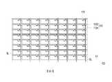
圖1是依照本發明的一實施例的一種元件基板的上視示意圖。圖2是依照本發明的一實施例的一種元件陣列的上視示意圖。為了方便說明,圖1省略繪示了元件陣列的具體結構。FIG. 1 is a schematic top view of a device substrate according to an embodiment of the invention. 2 is a schematic top view of an element array according to an embodiment of the invention. For convenience of description, FIG. 1 omits the specific structure of the element array.
請參考圖1與圖2,元件基板10包括載板100、元件陣列110、多條第一扇出線L1以及多條第二扇出線L2。在本實施例中,元件基板10還包括多條第三扇出線L3以及多條第四扇出線L4。1 and 2, the
載板100具有第一側邊S1、第二側邊S2、第三側邊S3以及第四側邊S4。第一側邊S1相對於第二側邊S2,且第三側邊S3相對於第四側邊S4。載板100之材質可為玻璃、石英、有機聚合物或是不透光/反射材料(例如:導電材料、金屬、晶圓、陶瓷、或其它可適用的材料)或是其它可適用的材料。若使用導電材料或金屬時,則在載板100上覆蓋一層絕緣層(未繪示),以避免短路問題。The
元件陣列110位於載板的第一面A上。元件陣列110包括多個子畫素112。各子畫素112包括切換元件1122以及光電元件1124。光電元件1124包括自發光元件或非自發光元件,舉例來說,光電元件1124包括發光二極體、畫素電極、光感測器或其他元件。在本實施例中,元件陣列110還包括多條掃描線SL以及多條資料線DL。掃描線SL電性連接至對應之切換元件1122的閘極,且資料線DL性連接至對應之切換元件1122的閘極源極。光電元件1124電性連接至切換元件1122的汲極。The
多條第一扇出線L1自載板100的第一側邊S1延伸至載板100的第一面A,且電性連接至元件陣列110。多條第二扇出線L2自載板100的第二側邊S2延伸至載板100的第一面A,且電性連接至元件陣列110。第一扇出線L1與第二扇出線L2電性連接至元件陣列110的掃描線SL或資料線DL。舉例來說,第一扇出線L1電性連接至部分資料線DL,且第二扇出線L2電性連接至另一部分資料線DL。在其他實施例中,第一扇出線L1電性連接至部分掃描線SL,且第二扇出線L2電性連接至另一部分掃描線SL。第一扇出線L1與第二扇出線L2將元件陣列110電性連接至驅動電路(未繪出),驅動電路位於載板100相對於第一面A之第二面(背面),藉此可以降低載板100周邊區的尺寸,使元件基板10具有窄邊框甚至無邊框的優點。A plurality of first fan-out lines L1 extend from the first side S1 of the
第一扇出線L1與第二扇出線L2非對稱地分別設置於第一側邊S1上與第二側邊S2上。第一扇出線L1於載板100的第一面A上沿著第一延伸方向E1延伸,且至少部分第一扇出線L1於第一延伸方向E1上不重疊於第二扇出線L2。在本實施例中,第一扇出線L1與第二扇出線L2皆於載板100的第一面A上沿著第一延伸方向E1延伸。資料線DL例如沿著第一延伸方向E1延伸。The first fan-out line L1 and the second fan-out line L2 are respectively disposed asymmetrically on the first side S1 and the second side S2. The first fan-out line L1 extends along the first extension direction E1 on the first surface A of the
多條第三扇出線L3自載板100的第三側邊S3延伸至載板100的第一面A,且電性連接至元件陣列110。多條第四扇出線L4自載板100的第四側邊S4延伸至載板100的第一面A,且電性連接至元件陣列110。第三扇出線L3與第四扇出線L4電性連接至元件陣列110的掃描線SL或資料線DL。舉例來說,第三扇出線L3電性連接至部分掃描線SL,且第四扇出線L4電性連接至另一部分掃描線SL。在其他實施例中,第三扇出線L3電性連接至部分資料線DL,且第四扇出線L4電性連接至另一部分資料線DL。第三扇出線L3與第四扇出線L4將元件陣列110電性連接至驅動電路(未繪出),驅動電路位於載板100相對於第一面A之第二面(背面),藉此可以降低載板100周邊區的尺寸,使元件基板10具有窄邊框甚至無邊框的優點。A plurality of third fan-out lines L3 extend from the third side S3 of the
第三扇出線L3與第四扇出線L4非對稱地分別設置於第三側邊S3上與第四側邊S4上。第三扇出線L3於載板100的第一面A上沿著第二延伸方向E2延伸,且至少部分第三扇出線L3於第二延伸方向E2上不重疊於第四扇出線L4。在本實施例中,第三扇出線L3與第四扇出線L4皆於載板100的第一面A上沿著第二延伸方向E2延伸。掃描線SL例如沿著第二延伸方向E2延伸。The third fan-out line L3 and the fourth fan-out line L4 are disposed asymmetrically on the third side S3 and the fourth side S4, respectively. The third fan-out line L3 extends along the second extension direction E2 on the first surface A of the
第一扇出線L1、第二扇出線L2、第三扇出線L3以及第四扇出線L4自載板100的第一面A彎折至載板100相對於第一面A的第二面(背面)。The first fan-out line L1, the second fan-out line L2, the third fan-out line L3, and the fourth fan-out line L4 are bent from the first surface A of the
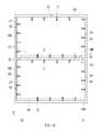
圖3A是依照本發明的一實施例的一種拼接電子裝置的上視示意圖。圖3B是沿著圖3A剖線aa’的剖面示意圖。為了方便說明,圖3A省略繪示了圖3B的絕緣層I,且圖3B省略繪示了圖3A中的固定件20。在此必須說明的是,圖3A和圖3B的實施例沿用圖1和圖2的實施例的元件標號與部分內容,其中採用相同或近似的標號來表示相同或近似的元件,並且省略了相同技術內容的說明。關於省略部分的說明可參考前述實施例,在此不贅述。3A is a schematic top view of a splicing electronic device according to an embodiment of the invention. Fig. 3B is a schematic cross-sectional view taken along line aa' of Fig. 3A. For convenience of description, FIG. 3A omits the insulating layer I of FIG. 3B, and FIG. 3B omits the fixing
請參考圖3A和圖3B,拼接電子裝置1包括兩個元件基板。在本實施例中,拼接電子裝置1包括元件基板10A以及元件基板10B。在本實施例中,電子裝置1還包括固定件20。在一些實施例中,元件基板10A以及元件基板10B藉由固定件20組合在一起。在一些實施例中,固定件20例如包括分別組裝於元件基板10A以及元件基板10B的兩個部分,接著在將前述固定件20的兩個部分互相結合。在一些實施例中,元件基板10A以及元件基板10B共同固定在一塊整塊的固定件20上。Please refer to FIGS. 3A and 3B, the splicing
兩個元件基板的其中一個之第一側邊相鄰於兩個元件基板的其中另一個之第二側邊。兩個元件基板的其中一個之該些第一扇出線與該兩個元件基板的其中另一個之該些第二扇出線互相不對稱。在本實施例中,元件基板10A之第一側邊S1相鄰於元件基板10B之第二側邊S2。元件基板10A之第一扇出線L1與元件基板10B之第二扇出線L2互相不對稱。元件基板10A之第一扇出線L1於第一延伸方向E1上不重疊於元件基板10B之第二扇出線L2。由於第一扇出線L1與第二扇出線L2互相不對稱,可以改善第一扇出線L1與第二扇出線L2之間訊號耦合的問題。因此,元件基板10A與元件基板10B之間的接縫可以較小。The first side of one of the two element substrates is adjacent to the second side of the other one of the two element substrates. The first fan-out lines of one of the two element substrates and the second fan-out lines of the other of the two element substrates are asymmetric to each other. In this embodiment, the first side S1 of the
在本實施例中,元件基板10A與元件基板10B還包括覆蓋第一扇出線L1、第二扇出線L2、第三扇出線L3以及第四扇出線L4的絕緣層I。絕緣層I自載板100的第一面A延伸至載板100相對於第一面A的第二面B,以包覆分別位於第一側邊S1、第二側邊S2、第三側邊S3以及第四側邊S4的第一扇出線L1、第二扇出線L2、第三扇出線L3以及第四扇出線L4。In this embodiment, the
4A是依照本發明的一實施例的一種拼接電子裝置的上視示意圖。圖4B是沿著圖4A剖線aa’的剖面示意圖。為了方便說明,圖4A省略繪示了圖4B的絕緣層I,且圖4B省略繪示了圖4A中的固定件20。在此必須說明的是,圖4A和圖4B的實施例沿用圖3A和圖3B的實施例的元件標號與部分內容,其中採用相同或近似的標號來表示相同或近似的元件,並且省略了相同技術內容的說明。關於省略部分的說明可參考前述實施例,在此不贅述。4A is a schematic top view of a splicing electronic device according to an embodiment of the invention. Fig. 4B is a schematic cross-sectional view taken along line aa' of Fig. 4A. For convenience of description, FIG. 4A omits the insulating layer I of FIG. 4B, and FIG. 4B omits the fixing
圖4A和圖4B之拼接電子裝置2與圖3A和圖3B之拼接電子裝置1的主要差異在於:拼接電子裝置2之元件基板10A的載板100於第一側邊S1處彎折。The main difference between the spliced
請參考圖4A和圖4B,元件基板10A與元件基板10B的載板100為可撓性載板,且元件基板10A的載板100於第一側邊S1處彎折,元件基板10B的載板100於第二側邊S2處彎折。4A and 4B, the
在本實施例中,元件基板10A與元件基板10B的第一扇出線L1、第二扇出線L2、第三扇出線L3以及第四扇出線L4皆形成於載板100的第一面A上,且元件基板10A與元件基板10B的載板100於第一側邊S1、第二側邊S2、第三側邊S3以及第四側邊S4處朝後彎折。藉由使載板100於第一側邊S1、第二側邊S2、第三側邊S3以及第四側邊S4處彎折,元件基板10A與元件基板10B的邊框面積較小,且元件基板10A與元件基板10B之間的接縫比較不明顯。In this embodiment, the first fan-out line L1, the second fan-out line L2, the third fan-out line L3, and the fourth fan-out line L4 of the
5A是依照本發明的一實施例的一種拼接電子裝置的上視示意圖。圖5B是沿著圖5A剖線aa’的剖面示意圖。為了方便說明,圖5A省略繪示了圖5B的第一軟性電路板P1、第二軟性電路板P2以及導線CL,且圖5B省略繪示了圖5A中的固定件20。在此必須說明的是,圖5A和圖5B的實施例沿用圖3A和圖3B的實施例的元件標號與部分內容,其中採用相同或近似的標號來表示相同或近似的元件,並且省略了相同技術內容的說明。關於省略部分的說明可參考前述實施例,在此不贅述。5A is a schematic top view of a splicing electronic device according to an embodiment of the invention. Fig. 5B is a schematic sectional view taken along the line aa' of Fig. 5A. For convenience of description, FIG. 5A omits the first flexible circuit board P1, the second flexible circuit board P2, and the leads CL of FIG. 5B, and FIG. 5B omits the fixing
圖5A和圖5B之拼接電子裝置3與圖3A和圖3B之拼接電子裝置1的主要差異在於:元件基板10A與元件基板10B各自包括第一軟性電路板P1以及第二軟性電路板P2。The main difference between the spliced
第一軟性電路板P1位於載板100的第一側邊S1上,且自載板100的第一面A彎折至載板100相對於第一面A的第二面B,其中第一扇出線L1位於第一軟性電路板P1上,且第一扇出線L1與載板100上的導線CL(例如為掃描線或資料線)電性連接。The first flexible circuit board P1 is located on the first side S1 of the
第二軟性電路板P2位於載板100的第二側邊S2上,且自載板100的第一面A彎折至載板100相對於第一面A的第二面B,其中第二扇出線L2位於第二軟性電路板P2上,且第二扇出線L2與載板100上的導線CL(例如為掃描線或資料線)電性連接。The second flexible circuit board P2 is located on the second side S2 of the
第三軟性電路板(未繪出)位於載板100的第三側邊S3上,且自載板100的第一面A彎折至載板100相對於第一面A的第二面B,其中第三扇出線L3位於第三軟性電路板上,且第三扇出線L3與載板100上的導線CL(例如為掃描線或資料線)電性連接。The third flexible circuit board (not shown) is located on the third side S3 of the
第四軟性電路板(未繪出)位於載板100的第四側邊S4上,且自載板100的第一面A彎折至載板100相對於第一面A的第二面B,其中第四扇出線L4位於第四軟性電路板上,且第四扇出線L4與載板100上的導線CL(例如為掃描線或資料線)電性連接。The fourth flexible circuit board (not shown) is located on the fourth side S4 of the
在一些實施例中,第一軟性電路板P1、第二軟性電路板P2、第三軟性電路板以及第四軟性電路板上還可以分別設置有驅動晶片(未繪出),但本發明不以此為限。In some embodiments, the first flexible circuit board P1, the second flexible circuit board P2, the third flexible circuit board, and the fourth flexible circuit board may also be provided with driver chips (not shown), but the present invention does not This is limited.
在一些實施例中,第一扇出線L1、第二扇出線L2、第三扇出線L3以及第四扇出線L4分別藉由導電結構(例如銲接材料、導電膠或其他導電構件)電性連接至導線CL。In some embodiments, the first fan-out line L1, the second fan-out line L2, the third fan-out line L3, and the fourth fan-out line L4 are respectively made of conductive structures (such as welding materials, conductive glue, or other conductive members) It is electrically connected to the wire CL.
綜上所述,第一扇出線L1與第二扇出線L2非對稱地分別設置於第一側邊S1上與第二側邊S2上,因此,能改善拼接電子裝置接縫過大的問題。In summary, the first fan-out line L1 and the second fan-out line L2 are disposed asymmetrically on the first side S1 and the second side S2, respectively, therefore, the problem of excessive seams of the spliced electronic device can be improved .
雖然本發明已以實施例揭露如上,然其並非用以限定本發明,任何所屬技術領域中具有通常知識者,在不脫離本發明的精神和範圍內,當可作些許的更動與潤飾,故本發明的保護範圍當視後附的申請專利範圍所界定者為準。Although the present invention has been disclosed as above with examples, it is not intended to limit the present invention. Any person with ordinary knowledge in the technical field can make some changes and modifications without departing from the spirit and scope of the present invention. The scope of protection of the present invention shall be subject to the scope defined in the appended patent application.
1、2、3:拼接電子裝置10、10A、10B:元件基板20:固定件100:載板110:元件陣列112:子畫素1122切換元件1124:光電元件A:第一面B:第二面CL:導線DL:資料線E1:第一延伸方向E2:第二延伸方向I:絕緣層L1:第一扇出線L2:第二扇出線L3:第三扇出線L4:第四扇出線P1:第一軟性電路板P2:第二軟性電路板S1:第一側邊S2:第二側邊S3:第三側邊S4:第四側邊SL:掃描線1, 2, 3: splicing
圖1是依照本發明的一實施例的一種元件基板的上視示意圖。 圖2是依照本發明的一實施例的一種元件陣列的上視示意圖。 圖3A是依照本發明的一實施例的一種拼接電子裝置的上視示意圖。 圖3B是沿著圖3A剖線aa’的剖面示意圖。 圖4A是依照本發明的一實施例的一種拼接電子裝置的上視示意圖。 圖4B是沿著圖4A剖線aa’的剖面示意圖。 5A是依照本發明的一實施例的一種拼接電子裝置的上視示意圖。 圖5B是沿著圖5A剖線aa’的剖面示意圖。FIG. 1 is a schematic top view of a device substrate according to an embodiment of the invention. 2 is a schematic top view of an element array according to an embodiment of the invention. 3A is a schematic top view of a splicing electronic device according to an embodiment of the invention. Fig. 3B is a schematic cross-sectional view taken along line aa' of Fig. 3A. 4A is a schematic top view of a splicing electronic device according to an embodiment of the invention. Fig. 4B is a schematic cross-sectional view taken along line aa' of Fig. 4A. 5A is a schematic top view of a splicing electronic device according to an embodiment of the invention. Fig. 5B is a schematic sectional view taken along the line aa' of Fig. 5A.
1:拼接電子裝置1: splicing electronic device
10A、10B:元件基板10A, 10B: component substrate
20:固定件20: fixings
100:載板100: carrier board
110:元件陣列110: element array
E1:第一延伸方向E1: First extension direction
E2:第二延伸方向E2: Second extension direction
L1:第一扇出線L1: the first fan-out line
L2:第二扇出線L2: second fan-out line
L3:第三扇出線L3: The third fan-out line
L4:第四扇出線L4: Fourth fan out
S1:第一側邊S1: first side
S2:第二側邊S2: second side
S3:第三側邊S3: third side
S4:第四側邊S4: Fourth side
Claims (11)
Translated fromChinesePriority Applications (4)
| Application Number | Priority Date | Filing Date | Title |
|---|---|---|---|
| TW108108862ATWI695215B (en) | 2019-03-15 | 2019-03-15 | Component substrate and splicing electronic device |
| US16/439,722US11495646B2 (en) | 2019-03-15 | 2019-06-13 | Device substrate with asymmetrical fan-out lines and spliced electronic apparatus using the same |
| CN201910966690.9ACN110738936B (en) | 2019-03-15 | 2019-10-12 | Component substrate and spliced electronic device |
| SG10201910890VASG10201910890VA (en) | 2019-03-15 | 2019-11-20 | Device substrate and spliced electronic apparatus |
Applications Claiming Priority (1)
| Application Number | Priority Date | Filing Date | Title |
|---|---|---|---|
| TW108108862ATWI695215B (en) | 2019-03-15 | 2019-03-15 | Component substrate and splicing electronic device |
Publications (2)
| Publication Number | Publication Date |
|---|---|
| TWI695215Btrue TWI695215B (en) | 2020-06-01 |
| TW202036128A TW202036128A (en) | 2020-10-01 |
Family
ID=69268799
Family Applications (1)
| Application Number | Title | Priority Date | Filing Date |
|---|---|---|---|
| TW108108862ATWI695215B (en) | 2019-03-15 | 2019-03-15 | Component substrate and splicing electronic device |
Country Status (4)
| Country | Link |
|---|---|
| US (1) | US11495646B2 (en) |
| CN (1) | CN110738936B (en) |
| SG (1) | SG10201910890VA (en) |
| TW (1) | TWI695215B (en) |
Families Citing this family (3)
| Publication number | Priority date | Publication date | Assignee | Title |
|---|---|---|---|---|
| US11444120B2 (en)* | 2020-01-14 | 2022-09-13 | Au Optronics Corporation | Display apparatus and method of fabricating the same |
| TWI737325B (en)* | 2020-06-01 | 2021-08-21 | 友達光電股份有限公司 | Display device and bezel thereof |
| CN116841127A (en)* | 2022-03-25 | 2023-10-03 | 京东方科技集团股份有限公司 | Array substrate and LCD panel |
Citations (2)
| Publication number | Priority date | Publication date | Assignee | Title |
|---|---|---|---|---|
| US20100238090A1 (en)* | 2007-04-05 | 2010-09-23 | Spectrum Dynamics Llc | Screen seaming device system and method |
| US20170148374A1 (en)* | 2015-11-20 | 2017-05-25 | Samsung Display Co., Ltd. | Display apparatus and tiled display apparatus |
Family Cites Families (16)
| Publication number | Priority date | Publication date | Assignee | Title |
|---|---|---|---|---|
| US6252564B1 (en) | 1997-08-28 | 2001-06-26 | E Ink Corporation | Tiled displays |
| US6897855B1 (en) | 1998-02-17 | 2005-05-24 | Sarnoff Corporation | Tiled electronic display structure |
| US6881946B2 (en)* | 2002-06-19 | 2005-04-19 | Eastman Kodak Company | Tiled electro-optic imaging device |
| KR100774911B1 (en) | 2003-10-14 | 2007-11-09 | 엘지전자 주식회사 | Electro luminescence display |
| US7926213B1 (en)* | 2007-04-13 | 2011-04-19 | Daktronics, Inc. | Electronic sign having slotted frame cabinets |
| KR20070002278A (en) | 2005-06-30 | 2007-01-05 | 삼성전자주식회사 | Display substrate and display device having same |
| WO2008126250A1 (en)* | 2007-03-30 | 2008-10-23 | Pioneer Corporation | Light emitting device |
| CN101718929B (en)* | 2009-10-23 | 2011-12-28 | 深超光电(深圳)有限公司 | Fan-out circuit of array substrate |
| TWI464484B (en)* | 2011-12-02 | 2014-12-11 | Au Optronics Corp | Fan-out circuit and electronic device having the same |
| GB2511549B (en) | 2013-03-07 | 2020-04-22 | Plastic Logic Ltd | Tiled Displays |
| TWI587768B (en) | 2014-09-12 | 2017-06-11 | 友達光電股份有限公司 | Display apparatus |
| TWI581225B (en)* | 2015-01-28 | 2017-05-01 | 友達光電股份有限公司 | Display device |
| CN206115896U (en) | 2016-10-27 | 2017-04-19 | 京东方科技集团股份有限公司 | Tiled display panel and tiled display device |
| US10468470B2 (en)* | 2017-02-27 | 2019-11-05 | Wuhan China Star Optoelectronics Technology Co., Ltd | OLED display module and method of forming the same |
| CN108122497B (en)* | 2018-02-02 | 2023-11-14 | 京东方科技集团股份有限公司 | A flexible array substrate, flexible display device and assembly method |
| US11094775B2 (en)* | 2018-06-15 | 2021-08-17 | Innolux Corporation | Tiled electronic device having a plurality of display panels and a flexible substrate |
- 2019
- 2019-03-15TWTW108108862Apatent/TWI695215B/enactive
- 2019-06-13USUS16/439,722patent/US11495646B2/enactiveActive
- 2019-10-12CNCN201910966690.9Apatent/CN110738936B/enactiveActive
- 2019-11-20SGSG10201910890VApatent/SG10201910890VA/enunknown
Patent Citations (2)
| Publication number | Priority date | Publication date | Assignee | Title |
|---|---|---|---|---|
| US20100238090A1 (en)* | 2007-04-05 | 2010-09-23 | Spectrum Dynamics Llc | Screen seaming device system and method |
| US20170148374A1 (en)* | 2015-11-20 | 2017-05-25 | Samsung Display Co., Ltd. | Display apparatus and tiled display apparatus |
Also Published As
| Publication number | Publication date |
|---|---|
| US20200295107A1 (en) | 2020-09-17 |
| CN110738936A (en) | 2020-01-31 |
| US11495646B2 (en) | 2022-11-08 |
| SG10201910890VA (en) | 2020-10-29 |
| TW202036128A (en) | 2020-10-01 |
| CN110738936B (en) | 2021-12-07 |
Similar Documents
| Publication | Publication Date | Title |
|---|---|---|
| KR102827526B1 (en) | Foldable display apparatus | |
| TWI767914B (en) | Display device having a bending region | |
| CN113169218B (en) | Display device | |
| KR102649145B1 (en) | display device | |
| US10840463B2 (en) | Display device | |
| CN113841194B (en) | Display device and display panel | |
| TWI695215B (en) | Component substrate and splicing electronic device | |
| US11304293B2 (en) | Display apparatus | |
| US11693458B2 (en) | Display apparatus | |
| CN114256310A (en) | Display device | |
| CN114695419A (en) | Displays and Video Walls | |
| JP7098425B2 (en) | Display device | |
| KR102674786B1 (en) | Multi screen display apparatus and method of manufacturing the same | |
| CN109358772A (en) | Touch screen and display device | |
| EP4287255B1 (en) | Display device, method of manufacturing the same, and tiled display device including the same | |
| TWI666490B (en) | Electronic device | |
| CN116322182A (en) | Display device and multi-screen display device including the same | |
| KR102721400B1 (en) | Display device and display device manufacturing method | |
| US20220304154A1 (en) | Display panel and display apparatus | |
| JP2006210809A (en) | Wiring board, mounting structure, electro-optical device, and electronic apparatus | |
| US12328835B2 (en) | Display apparatus | |
| TWI687739B (en) | Display appratus | |
| TWI498654B (en) | Pixel array substrate and display panel | |
| WO2025086206A1 (en) | Display substrate and display device | |
| TW202422171A (en) | Display apparatus |