TWI695120B - Micro fluid actuator - Google Patents
Micro fluid actuatorDownload PDFInfo
- Publication number
- TWI695120B TWI695120BTW108101560ATW108101560ATWI695120BTW I695120 BTWI695120 BTW I695120BTW 108101560 ATW108101560 ATW 108101560ATW 108101560 ATW108101560 ATW 108101560ATW I695120 BTWI695120 BTW I695120B
- Authority
- TW
- Taiwan
- Prior art keywords
- layer
- holes
- fluid
- etching process
- metal layer
- Prior art date
Links
- 239000012530fluidSubstances0.000titleclaimsabstractdescription82
- 229910052751metalInorganic materials0.000claimsabstractdescription81
- 239000002184metalSubstances0.000claimsabstractdescription81
- 239000000758substrateSubstances0.000claimsabstractdescription64
- 238000003860storageMethods0.000claimsabstractdescription26
- 238000000034methodMethods0.000claimsdescription135
- 230000008569processEffects0.000claimsdescription133
- 238000005530etchingMethods0.000claimsdescription61
- 229920002120photoresistant polymerPolymers0.000claimsdescription47
- 238000005137deposition processMethods0.000claimsdescription33
- 238000002955isolationMethods0.000claimsdescription26
- 230000004888barrier functionEffects0.000claimsdescription16
- 239000000463materialSubstances0.000claimsdescription14
- VYPSYNLAJGMNEJ-UHFFFAOYSA-NSilicium dioxideChemical groupO=[Si]=OVYPSYNLAJGMNEJ-UHFFFAOYSA-N0.000claimsdescription12
- 239000007769metal materialSubstances0.000claimsdescription12
- 238000011161developmentMethods0.000claimsdescription11
- 238000005096rolling processMethods0.000claimsdescription10
- 230000005540biological transmissionEffects0.000claimsdescription8
- 238000000576coating methodMethods0.000claimsdescription7
- 238000006073displacement reactionMethods0.000claimsdescription7
- 238000004891communicationMethods0.000claimsdescription6
- 235000012239silicon dioxideNutrition0.000claimsdescription6
- 239000000377silicon dioxideSubstances0.000claimsdescription6
- 238000000708deep reactive-ion etchingMethods0.000claimsdescription5
- 238000001312dry etchingMethods0.000claimsdescription4
- 238000001459lithographyMethods0.000claimsdescription4
- 238000007747platingMethods0.000claimsdescription4
- 238000001039wet etchingMethods0.000claimsdescription4
- 238000010329laser etchingMethods0.000claimsdescription3
- 229910052581Si3N4Inorganic materials0.000claimsdescription2
- XUIMIQQOPSSXEZ-UHFFFAOYSA-NSiliconChemical compound[Si]XUIMIQQOPSSXEZ-UHFFFAOYSA-N0.000claimsdescription2
- NRTOMJZYCJJWKI-UHFFFAOYSA-NTitanium nitrideChemical group[Ti]#NNRTOMJZYCJJWKI-UHFFFAOYSA-N0.000claimsdescription2
- XAGFODPZIPBFFR-UHFFFAOYSA-NaluminiumChemical group[Al]XAGFODPZIPBFFR-UHFFFAOYSA-N0.000claimsdescription2
- PCHJSUWPFVWCPO-UHFFFAOYSA-NgoldChemical group[Au]PCHJSUWPFVWCPO-UHFFFAOYSA-N0.000claimsdescription2
- 239000010931goldSubstances0.000claimsdescription2
- 229910052737goldInorganic materials0.000claimsdescription2
- 229910052710siliconInorganic materials0.000claimsdescription2
- 239000010703siliconSubstances0.000claimsdescription2
- HQVNEWCFYHHQES-UHFFFAOYSA-Nsilicon nitrideChemical groupN12[Si]34N5[Si]62N3[Si]51N64HQVNEWCFYHHQES-UHFFFAOYSA-N0.000claimsdescription2
- GUVRBAGPIYLISA-UHFFFAOYSA-Ntantalum atomChemical group[Ta]GUVRBAGPIYLISA-UHFFFAOYSA-N0.000claimsdescription2
- 238000003466weldingMethods0.000claimsdescription2
- 230000008021depositionEffects0.000claims1
- 239000007788liquidSubstances0.000abstract2
- 239000010410layerSubstances0.000description221
- 239000012790adhesive layerSubstances0.000description9
- 239000004642PolyimideSubstances0.000description7
- 229920001721polyimidePolymers0.000description7
- 239000010409thin filmSubstances0.000description6
- 239000010408filmSubstances0.000description5
- 238000012545processingMethods0.000description5
- 238000009623Bosch processMethods0.000description4
- 238000005516engineering processMethods0.000description4
- 238000013461designMethods0.000description3
- 238000010586diagramMethods0.000description3
- 239000000126substanceSubstances0.000description3
- 230000009471actionEffects0.000description2
- 239000011248coating agentSubstances0.000description2
- 238000009826distributionMethods0.000description2
- 238000004519manufacturing processMethods0.000description2
- 230000035515penetrationEffects0.000description2
- 238000005240physical vapour depositionMethods0.000description2
- 229920000052poly(p-xylylene)Polymers0.000description2
- 238000007639printingMethods0.000description2
- 239000000047productSubstances0.000description2
- 239000011265semifinished productSubstances0.000description2
- 125000006850spacer groupChemical group0.000description2
- 230000008961swellingEffects0.000description2
- 230000004913activationEffects0.000description1
- 238000004026adhesive bondingMethods0.000description1
- 230000009286beneficial effectEffects0.000description1
- 238000006243chemical reactionMethods0.000description1
- 239000003795chemical substances by applicationSubstances0.000description1
- 239000003814drugSubstances0.000description1
- 230000000694effectsEffects0.000description1
- 230000003628erosive effectEffects0.000description1
- 239000011521glassSubstances0.000description1
- 230000017525heat dissipationEffects0.000description1
- 238000007731hot pressingMethods0.000description1
- 239000012535impuritySubstances0.000description1
- 230000028161membrane depolarizationEffects0.000description1
- 238000012536packaging technologyMethods0.000description1
- 238000002791soakingMethods0.000description1
- 238000004528spin coatingMethods0.000description1
- 229910001220stainless steelInorganic materials0.000description1
- 239000010935stainless steelSubstances0.000description1
- 230000008646thermal stressEffects0.000description1
- 239000011800void materialSubstances0.000description1
Images


Classifications
- F—MECHANICAL ENGINEERING; LIGHTING; HEATING; WEAPONS; BLASTING
- F16—ENGINEERING ELEMENTS AND UNITS; GENERAL MEASURES FOR PRODUCING AND MAINTAINING EFFECTIVE FUNCTIONING OF MACHINES OR INSTALLATIONS; THERMAL INSULATION IN GENERAL
- F16K—VALVES; TAPS; COCKS; ACTUATING-FLOATS; DEVICES FOR VENTING OR AERATING
- F16K99/00—Subject matter not provided for in other groups of this subclass
- F16K99/0001—Microvalves
- F16K99/0034—Operating means specially adapted for microvalves
- F16K99/0042—Electric operating means therefor
- F16K99/0048—Electric operating means therefor using piezoelectric means
- F—MECHANICAL ENGINEERING; LIGHTING; HEATING; WEAPONS; BLASTING
- F04—POSITIVE - DISPLACEMENT MACHINES FOR LIQUIDS; PUMPS FOR LIQUIDS OR ELASTIC FLUIDS
- F04B—POSITIVE-DISPLACEMENT MACHINES FOR LIQUIDS; PUMPS
- F04B43/00—Machines, pumps, or pumping installations having flexible working members
- F04B43/02—Machines, pumps, or pumping installations having flexible working members having plate-like flexible members, e.g. diaphragms
- F04B43/04—Pumps having electric drive
- F04B43/043—Micropumps
- F04B43/046—Micropumps with piezoelectric drive
- B—PERFORMING OPERATIONS; TRANSPORTING
- B81—MICROSTRUCTURAL TECHNOLOGY
- B81C—PROCESSES OR APPARATUS SPECIALLY ADAPTED FOR THE MANUFACTURE OR TREATMENT OF MICROSTRUCTURAL DEVICES OR SYSTEMS
- B81C1/00—Manufacture or treatment of devices or systems in or on a substrate
- B81C1/00015—Manufacture or treatment of devices or systems in or on a substrate for manufacturing microsystems
- B81C1/00023—Manufacture or treatment of devices or systems in or on a substrate for manufacturing microsystems without movable or flexible elements
- F—MECHANICAL ENGINEERING; LIGHTING; HEATING; WEAPONS; BLASTING
- F16—ENGINEERING ELEMENTS AND UNITS; GENERAL MEASURES FOR PRODUCING AND MAINTAINING EFFECTIVE FUNCTIONING OF MACHINES OR INSTALLATIONS; THERMAL INSULATION IN GENERAL
- F16K—VALVES; TAPS; COCKS; ACTUATING-FLOATS; DEVICES FOR VENTING OR AERATING
- F16K99/00—Subject matter not provided for in other groups of this subclass
- F16K99/0001—Microvalves
- F16K99/0003—Constructional types of microvalves; Details of the cutting-off member
- F—MECHANICAL ENGINEERING; LIGHTING; HEATING; WEAPONS; BLASTING
- F16—ENGINEERING ELEMENTS AND UNITS; GENERAL MEASURES FOR PRODUCING AND MAINTAINING EFFECTIVE FUNCTIONING OF MACHINES OR INSTALLATIONS; THERMAL INSULATION IN GENERAL
- F16K—VALVES; TAPS; COCKS; ACTUATING-FLOATS; DEVICES FOR VENTING OR AERATING
- F16K99/00—Subject matter not provided for in other groups of this subclass
- F16K2099/0082—Microvalves adapted for a particular use
- F16K2099/0086—Medical applications
Landscapes
- Engineering & Computer Science (AREA)
- General Engineering & Computer Science (AREA)
- Chemical & Material Sciences (AREA)
- Mechanical Engineering (AREA)
- Dispersion Chemistry (AREA)
- Manufacturing & Machinery (AREA)
- Analytical Chemistry (AREA)
- Microelectronics & Electronic Packaging (AREA)
- Micromachines (AREA)
Abstract
Description
Translated fromChinese本案關於一種致動器,尤指一種使用微機電面型及體型加工製程製作之微流體致動器。This case relates to an actuator, in particular to a microfluidic actuator manufactured using micro-electromechanical surface and body processing processes.
目前於各領域中無論是醫藥、電腦科技、列印、能源等工業,產品均朝精緻化及微小化方向發展,其中微幫浦、噴霧器、噴墨頭、工業列印裝置等產品所包含之流體致動器為其關鍵技術。At present, in all fields, whether it is medicine, computer technology, printing, energy and other industries, products are developing towards refinement and miniaturization. Among them, micro-pumps, sprayers, inkjet heads, industrial printing devices and other products are included Fluid actuators are its key technology.
隨著科技的日新月異,流體輸送結構的應用上亦愈來愈多元化,舉凡工業應用、生醫應用、醫療保健、電子散熱……等,甚至近來熱門的穿戴式裝置皆可見它的踨影,可見傳統的流體致動器已漸漸有朝向裝置微小化、流量極大化的趨勢。With the rapid development of technology, the application of fluid transport structure is becoming more and more diversified. For example, industrial applications, biomedical applications, medical care, electronic heat dissipation, etc., and even the most popular wearable devices can be seen in recent years. It can be seen that the traditional fluid actuators have gradually tended to miniaturize the device and maximize the flow rate.
現有技術中已發展多種微機電製程製出之微流體致動器,然而,藉創新結構增進流體傳輸之功效,仍為發展之重要內容。Microfluidic actuators produced by various microelectromechanical processes have been developed in the prior art. However, it is still an important content for development to improve the efficiency of fluid transmission by innovative structures.
本案之主要目的係提供一種有閥式微流體致動器,使用微機電製程製作,可傳輸流體。本案之微流體致動器使用微機電面型及體型加工製程,並輔以封裝技術製作而成。The main purpose of this case is to provide a valve-type microfluidic actuator, which is manufactured using a micro-electromechanical process and can transmit fluid. The microfluidic actuator in this case is manufactured using micro-electromechanical surface and body processing processes, supplemented by packaging technology.
本案之一廣義實施態樣為一種微流體致動器,包含:一基板、一腔體層、一振動層、一第一金屬層、一壓電致動層、一隔離層、一第二金屬層、一防水層、一光阻層、一入口層、一流道層、一共振層以及一陣列孔片。基板具有一第一表面及一第二表面,並透過蝕刻製程形成一出口溝槽、複數個第一出流孔洞以及複數個第二出流孔洞。出口溝槽與複數個第一出流孔洞以及複數個第二出流孔洞相連通。複數個第二出流孔洞設置在複數個第一出流孔洞的外側。腔體層透過沉積製程形成於基板之第一表面上,且透過蝕刻製程形成一儲流腔室。儲流腔室與複數個第一出流孔洞以及複數個第二出流孔洞相連通。振動層透過沉積製程形成於腔體層上,且透過蝕刻製程形成複數個流體溝槽以及一振動區。複數個流體溝槽對稱形成於振動層之相對兩側,藉以定義出振動區。第一金屬層透過沉積製程形成於振動層上,且透過蝕刻製程形成一下電極區、複數個阻障區以及複數個間隙。下電極區形成於對應振動區的位置。複數個間隙形成於下電極區與複數個阻障區之間。複數個阻障區對應形成於複數個流體溝槽之外側位置。壓電致動層透過沉積製程形成於第一金屬層上,且透過蝕刻製程於對應第一金屬層之下電極區的位置形成一作動區。隔離層透過沉積製程形成於壓電致動層與第一金屬層上,且透過蝕刻製程於複數個間隙內形成複數個間隙壁。第二金屬層透過沉積製程形成於壓電致動層、第一金屬層以及隔離層上,且透過蝕刻製程於第一金屬層上形成一上電極焊墊以及一下電極焊墊。防水層透過鍍膜製程形成於第一金屬層、第二金屬層以及隔離層上,並透過蝕刻製程露出上電極焊墊以及下電極焊墊。光阻層透過顯影製程形成於第一金屬層、第二金屬層以及防水層上。入口層透過蝕刻製程或雷射製程形成複數個流體入口。流道層形成於入口層上,且透過微影製程形成一入流腔室、複數個入流通道以及複數個流道入口。複數個流道入口分別與入口層之複數個流體入口相連通。複數個入流通道以及複數個流道入口圍繞設置於入流腔室周圍。複數個入流通道連通於複數個流道入口與入流腔室之間。共振層透過滾壓製程形成於流道層上,透過蝕刻製程形成一腔體通孔,且透過翻轉對位製程以及晶圓接合製程接合於光阻層上。陣列孔片透過黏貼製程形成於基板上。陣列孔片具有複數個孔片孔洞。複數個孔片孔洞與複數個第一出流孔洞以及複數個第二出流孔洞相互錯位設置,藉此封閉第一基板之複數個第一出流孔洞以及複數個第二出流孔洞。提供具有不同相位電荷之驅動電源至上電極焊墊以及下電極焊墊,以驅動並控制振動層之振動區產生上下位移,使流體自複數個流體入口吸入,通過複數個入流通道流至入流腔室,再通過腔體通孔流至共振腔室,最後通過複數個流體溝槽流至儲流腔室,再最後受擠壓經由複數個第一出流孔洞以及複數個第二出流孔洞並推開陣列孔片後自複數個孔片孔洞排出以完成流體傳輸。A broad implementation aspect of this case is a microfluidic actuator, which includes: a substrate, a cavity layer, a vibrating layer, a first metal layer, a piezoelectric actuation layer, an isolation layer, and a second metal layer , A waterproof layer, a photoresist layer, an entrance layer, a channel layer, a resonance layer and an array of holes. The substrate has a first surface and a second surface, and an exit trench, a plurality of first outflow holes, and a plurality of second outflow holes are formed through an etching process. The outlet groove communicates with the plurality of first outflow holes and the plurality of second outflow holes. The plurality of second outflow holes are disposed outside the plurality of first outflow holes. The cavity layer is formed on the first surface of the substrate through a deposition process, and a current storage chamber is formed through an etching process. The storage chamber is in communication with a plurality of first outflow holes and a plurality of second outflow holes. The vibration layer is formed on the cavity layer through a deposition process, and a plurality of fluid grooves and a vibration region are formed through an etching process. A plurality of fluid grooves are formed symmetrically on opposite sides of the vibration layer, thereby defining a vibration area. The first metal layer is formed on the vibration layer through a deposition process, and an electrode region, a plurality of barrier regions, and a plurality of gaps are formed through an etching process. The lower electrode area is formed at a position corresponding to the vibration area. A plurality of gaps are formed between the lower electrode area and the plurality of barrier areas. The plurality of barrier regions are correspondingly formed at positions outside the plurality of fluid grooves. The piezoelectric actuation layer is formed on the first metal layer through a deposition process, and an actuation region is formed at a position corresponding to the electrode region under the first metal layer through an etching process. The isolation layer is formed on the piezoelectric actuation layer and the first metal layer through a deposition process, and a plurality of gap walls are formed in the plurality of gaps through an etching process. The second metal layer is formed on the piezoelectric actuator layer, the first metal layer, and the isolation layer through a deposition process, and an upper electrode pad and a lower electrode pad are formed on the first metal layer through an etching process. The waterproof layer is formed on the first metal layer, the second metal layer, and the isolation layer through a plating process, and exposes the upper electrode pad and the lower electrode pad through the etching process. The photoresist layer is formed on the first metal layer, the second metal layer, and the waterproof layer through a development process. The inlet layer forms a plurality of fluid inlets through an etching process or a laser process. The flow channel layer is formed on the inlet layer, and an inflow chamber, a plurality of inflow channels, and a plurality of flow channel inlets are formed through the lithography process. The plurality of flow channel inlets respectively communicate with the plurality of fluid inlets of the inlet layer. A plurality of inflow channels and a plurality of flow channel inlets are arranged around the inflow chamber. The plurality of inflow channels are connected between the inlets of the plurality of flow channels and the inflow chamber. The resonance layer is formed on the flow channel layer through a rolling process, a cavity through-hole is formed through an etching process, and is bonded to the photoresist layer through a flip alignment process and a wafer bonding process. The array orifice is formed on the substrate through a bonding process. The array hole plate has a plurality of hole plates. The plurality of orifice holes and the plurality of first outflow holes and the plurality of second outflow holes are offset from each other, thereby closing the plurality of first outflow holes and the plurality of second outflow holes of the first substrate. Provide driving power with different phase charges to the upper electrode pad and the lower electrode pad to drive and control the vibration area of the vibration layer to generate up and down displacement, so that the fluid is sucked from the plurality of fluid inlets and flows into the inflow chamber through the plurality of inflow channels , Then flow through the cavity through hole to the resonance chamber, and finally flow through the plurality of fluid grooves to the storage chamber, and then finally squeezed through the plurality of first outflow holes and the plurality of second outflow holes and push After opening the array orifice, it is discharged from the holes of the orifices to complete the fluid transmission.
體現本案特徵與優點的一些典型實施例將在後段的說明中詳細敘述。應理解的是本案能夠在不同的態樣上具有各種的變化,其皆不脫離本案的範圍,且其中的說明及圖示在本質上當作說明之用,而非用以限制本案。Some typical embodiments embodying the characteristics and advantages of this case will be described in detail in the description in the following paragraphs. It should be understood that this case can have various changes in different forms, which all do not deviate from the scope of this case, and the descriptions and illustrations therein are essentially used for explanation rather than to limit this case.
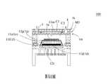
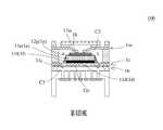
本案之微流體致動器用於輸送流體,請參閱第1A圖以及第1B圖,於本案實施例中,微流體致動器100包含:一第一基板1a、一腔體層1b、一振動層1c、一第一金屬層1d、一壓電致動層1e、一隔離層1f、一第二金屬層1g、一防水層1h、一第二基板1i、一薄膜膠層1j、一入口層1k、一共振層1m、一罩幕層1n、一陣列孔片1o、一第一光阻層M1、一第二光阻層M2、一流道層M3以及一第三光阻層M4。陣列孔片1o、第一基板1a、腔體層1b、振動層1c、第一金屬層1d、壓電致動層1e、隔離層1f、第二金屬層1g、防水層1h、第二光阻層M2、共振層1m、流道層M3以及入口層1k係依序堆疊結合後形成為一體,其製程如下說明。於本案第一實施例中,微流體致動器100包含一致動單元10。The microfluidic actuator of this case is used to transport fluids. Please refer to FIGS. 1A and 1B. In the embodiment of this case, the
請參閱第2A圖,於本案第一實施例中,第一基板1a為一矽基材。第一基板1a具有一第一表面11a以及一相對於第一表面11a之第二表面12a。於本案第一實施例中,腔體層1b透過一二氧化矽材料沉積製程形成於第一基板1a之第一表面11a之上,沉積製程可為一物理氣相沉積製程(PVD)、一化學氣相沉積製程(CVD)或兩者之組合,但不以此為限。於本案第一實施例中,振動層1c透過一氮化矽材料沉積製程形成於腔體層1b之上。Please refer to FIG. 2A. In the first embodiment of the present case, the
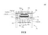
請參閱第2B圖以及第3圖,於本案第一實施例中,振動層1c透過一蝕刻製程形成複數個流體溝槽11c以及一振動區12c。流體溝槽11c對稱形成於振動層1c的相對兩側,藉以定義出振動區12c。值得注意的是,於本案第一實施例中,蝕刻製程可為一濕式蝕刻製程、一乾式蝕刻製程或兩者之組合,但不以此為限。值得注意的是,於本案第一實施例中,振動層1c,具有二流體溝槽11c,分別形成於振動層1c縱向的相對兩側,但不以此為限。Please refer to FIG. 2B and FIG. 3, in the first embodiment of the present invention, the
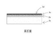
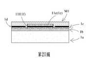
請參閱第2C圖以及第2D圖,於本案第一實施例中,第一金屬層1d透過一第一金屬材料沉積製程形成於振動層1c之上。於本案實施例中,第一金屬材料為一氮化鈦金屬材料或一鉭金屬材料,但不以此為限。第一金屬層1d透過蝕刻製程形成一下電極區11d、複數個阻障區12d、複數個間隙13d以及複數個第一接合對位記號AM1。下電極區11d形成於對應振動層1c之振動區12c的位置。間隙13d形成於下電極區11d與阻障區12d之間。阻障區12d對應形成於振動層1c之流體溝槽11c的外側位置。第一接合對位記號AM1形成於阻障區12d之上。Please refer to FIG. 2C and FIG. 2D. In the first embodiment of the present invention, the
請參閱第2E圖以及第2F圖,於本案第一實施例中,壓電致動層1e透過一壓電材料沉積製程形成於第一金屬層1d之上,且透過蝕刻製程於對應第一金屬層1d之下電極區11d的位置形成一作動區11e。Please refer to FIGS. 2E and 2F. In the first embodiment of the present invention, the piezoelectric actuation layer 1e is formed on the
請參閱第2G圖以及第2H圖,於本案第一實施例中,隔離層1f透過一二氧化矽材料沉積製程形成於第一金屬層1d以及壓電致動層1e上,且透過蝕刻製程於第一金屬層1d之間隙13d內形成複數個間隙壁11f。Please refer to FIG. 2G and FIG. 2H. In the first embodiment of this case, the
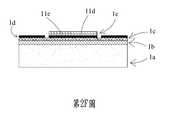
請參閱第2I圖以及第2J圖,於本案第一實施例中,第一光阻層M1透過一光阻塗佈製程形成於第一金屬層1d、壓電致動層1e以及隔離層1f上,並透過一顯影製程形成一第一光阻區M1a。值得注意的是,光阻塗佈製程可為一旋塗(Spin Coating)製程或一層壓(Laminate Rolling)製程,但不以此為限,得以依照製程需求作變更。於本案第一實施例中,第一光阻層M1為一負光阻,但不以此為限。Please refer to FIG. 2I and FIG. 2J. In the first embodiment of the present case, the first photoresist layer M1 is formed on the
請參閱第2K圖、第2L圖以及第3圖,於本案第一實施例中,第二金屬層1g透過一第二金屬材料沉積製程形成於第一金屬層1d、壓電致動層1e、該隔離層1f以及第一光阻層M1之第一光阻區M1a之上。於本案第一實施例中,第二金屬材料為一金金屬材料或一鋁金屬材料,但不以此為限。第二金屬層1g透過一掀離(Lift-Off)製程將第一光阻層M1移除,藉以形成一焊墊隔離區11g、一上電極區12g、一上電極焊墊13g以及一下電極焊墊14g。上電極區12g形成於壓電致動層1e之作動區11e之上。上電極焊墊13g以及下電極焊墊14g形成於第一金屬層1d之上,並位於壓電致動層1e之作動區11e之相對兩側。上電極區12g與下電極焊墊14g藉由焊墊隔離區11g相分離。Please refer to FIG. 2K, FIG. 2L and FIG. 3. In the first embodiment of this case, the
請參閱第2M圖,於本案第一實施例中,防水層1h透過一鍍膜製程形成於第一金屬層1d、第二金屬層1g以及隔離層1f上,並透過蝕刻製程露出第二金屬層1g之上電極焊墊13g以及下電極焊墊14g。值得注意的是,於本案第一實施例中,防水層1h為一聚對二甲苯(Parylene)材質,但不以此為限。聚對二甲苯可於室溫下鍍膜,並且具有包覆性強、耐化性高以及生物相容性佳等優點。值得注意的是,防水層1h的設置,可避免第一金屬層1d、壓電致動層1e以及第二金屬層1g遭流體腐蝕而產生短路現象。Please refer to FIG. 2M. In the first embodiment of this case, the
請參閱第2N圖以及第2O圖,於本案第一實施例中,第二光阻層M2透過光阻塗佈製程形成於第一金屬層1d、第二金屬層1g以及防水層1h上,並透過顯影製程形成複數個第二光阻孔洞M2a以及一第二光阻開口M2b。Please refer to FIG. 2N and FIG. 2O. In the first embodiment of this case, the second photoresist layer M2 is formed on the
請參閱第2P圖、第2Q圖以及第4圖,於本案第一實施例中,第二基板1i為一玻璃基板。薄膜膠層1j透過一滾壓製程形成於第二基板1i上。入口層1k透過滾壓製程形成於薄膜膠層1j。於本案第一實施例中,入口層1k為一聚醯亞胺(Polyimide, PI)材質,但不以此為限。薄膜膠層1j以及入口層1k透過蝕刻製程形成複數個流體入口I以及複數個接合對位記號窗AW。接合對位記號窗AW形成於流體入口I之外側。值得注意的是,成形流體入口I以及接合對位記號窗AW之蝕刻製程為一乾蝕刻製程或一雷射蝕刻製程,但不以此為限。於本案第一實施例中,微流體致動器100具有四個流體入口I,分別位於微流體致動器100之四個角落,於其他實施例中,流體入口I的數量以及分佈方式得依設計需求而變化。Please refer to FIG. 2P, FIG. 2Q and FIG. 4, in the first embodiment of this case, the second substrate 1i is a glass substrate. The
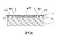
請參閱第2R圖、第2S圖以及第4圖,於本案第一實施例中,流道層M3透過光阻塗佈製程形成於入口層1k上,且透過顯影製程形成複數個流道入口M31、一腔體開口M32以及複數個入流通道M33。流道入口M31分別與入口層1k之流體入口I相連通。流道入口M31以及入流通道M33圍繞設置在腔體開口M32周圍。入流通道M33連通於流道入口M31與腔體開口M32之間。於本案第一實施例中,流道層M3具有四個流道入口M31以及四個入流通道M33,於其他實施例中,流道入口M31以及入流通道M33的數量可以設計需求而變更,不以此為限。於本案第一實施例中,流道層M3為一厚膜光阻,但不以此為限。Please refer to FIG. 2R, FIG. 2S, and FIG. 4, in the first embodiment of this case, the flow channel layer M3 is formed on the
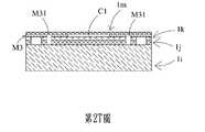
請參閱第2T圖以及第2U圖,於本案第一實施例中,共振層1m透過滾壓製程形成於流道層M3上,且透過蝕刻製程形成一腔體通孔11m以及複數個第二接合對位記號AM2。共振層1m覆蓋流道層M3之腔體開口M32,藉以定義出一入流腔室C1。腔體通孔11m與流道層M3之入流腔室C1相連通。第二接合對位記號AM2形成於共振層1m之外側。共振層1m自腔體通孔11m向外延伸至對應入流腔室C1外緣處定義為一可動部12m。共振層1m自可動部12m向外延伸至第二接合對位記號AM2處定義為一固定部13m。值得注意的是,成形共振層1m之蝕刻製程為乾蝕刻製程或雷射蝕刻製程,但不以此為限。Please refer to FIG. 2T and FIG. 2U. In the first embodiment of the present invention, a
請參閱第2V圖,於本案第一實施例中,共振層1m透過一翻轉對位製程以及一晶圓接合製程接合於第二光阻層M2上。於翻轉對位製程時,利用接合對位記號窗AW與相對應之第一接合對位記號AM1以及相對應之第二接合對位記號AM2相對準,以完成對位製程。值得注意的是,於本案第一實施例中,由於流道層M3以及第二基板1i呈透光性,於翻轉對位製程時,可藉由正面透視對位(Top-Side Transparent Alignment)方法進行人工對位,因此對位精度需求為±10μm。於本案第一實施例中,共振層1m為一聚醯亞胺(Polyimide, PI)材質,但不以此為限。Please refer to FIG. 2V. In the first embodiment of the present invention, the
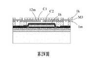
請參閱第2W圖,於本案第一實施例中,第二基板1i藉由將薄膜膠層1j浸泡藥劑使薄膜膠層1j失去黏性而移除。值得注意的是,於本案第一實施例中,浸泡薄膜膠層1j所需的時間極短,並且薄膜膠層1j與流道層M3的材質特性不同,因此藥劑不會對流道層M3起反應,也不會產生泡脹(Swelling)的問題。Please refer to FIG. 2W. In the first embodiment of the present invention, the second substrate 1i is removed by soaking the thin
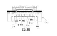
請參閱第2X圖至第2Z圖,於本案第一實施例中,罩幕層1n透過一二氧化矽材料沉積製程形成於第一基板1a之第二表面12a上,且透過蝕刻製程形成一罩幕開口11n以及複數個罩幕孔洞12n,使得第一基板1a露出。第一基板1a之第二表面12a分別沿著罩幕開口11n以及罩幕孔洞12n,透過蝕刻製程形成一出口溝槽13a以及複數個輔助溝槽14a。出口溝槽13a以及輔助溝槽14a具有相同之蝕刻深度,且蝕刻深度為蝕刻至第一表面11a以及第二表面12a之間且不與腔體層1b接觸。輔助溝槽14a對稱設置在出口溝槽13a的相對兩側。每一輔助溝槽14a與出口溝槽13a之間形成一定位柱P。Please refer to FIGS. 2X to 2Z. In the first embodiment of the present invention, the
請參閱第2AA圖及第2AB圖,於本案第一實施例中,罩幕層1n再透過一二氧化矽材料沉積製程形成於第一基板1a之出口溝槽13a以及輔助溝槽14a內,且透過一精密穿孔製程於出口溝槽13a內形成複數個第一罩幕通孔13n以及複數個第二罩幕通孔14n。第二罩幕通孔14n對稱設置於第一罩幕通孔13n的外側。於本案第一實施例中,第一罩幕通孔13n之孔徑小於第二罩幕通孔14n之孔徑,但不以此為限。第一罩幕通孔13n以及第二罩幕通孔14n之穿孔深度為至與第一基板1a接觸為止,使得第一基板1a得以露出。於本案第一實施例中,精密穿孔製程為一準分子雷射加工製程,但不以此為限。Please refer to FIG. 2AA and FIG. 2AB. In the first embodiment of this case, the
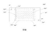
請參閱第2AC圖、第2AD圖以及第5圖,於本案第一實施例中,第一基板1a透過一低溫深蝕刻製程蝕刻第一基板1a對應於第一罩幕通孔13n以及第二罩幕通孔14n的部分,藉以形成第一基板1a之複數個第一出流孔洞15a以及複數個第二出流孔洞16a。第一出流孔洞15a為分別沿第一罩幕通孔13n蝕刻至與腔體層1b接觸為止所構成,以及第二出流孔洞16a為分別沿第二罩幕通孔14n蝕刻至與腔體層1b接觸為止所構成。藉此,第二出流孔洞16a設置在第一出流孔洞15a的外側,並且每一第二出流孔洞16a之孔徑大於每一第一出流孔洞15a之孔徑。於本案第一實施例中,低溫深蝕刻製程為一深反應性離子蝕刻製程(BOSCH Process),但不以此為限。於本案第一實施例中,每一第一出流孔洞15a以及每一第二出流孔洞16a具有方形之截面,但不以此為限。Please refer to FIG. 2AC, FIG. 2AD and FIG. 5, in the first embodiment of the present case, the
值得注意的是,於本案第一實施例中,罩幕層1n利用準分子雷射加工製程形成第一罩幕通孔13n以及第二罩幕通孔14n來克服光阻不易塗佈以及接觸式光罩曝光難以聚焦等問題。此外,於本案第一實施例中,深反應性離子蝕刻製程(BOSCH Process)屬於低溫製程,可避免加工所產生的高溫,影響後端壓電材料之極性分布,造成退極化反應。再者,於本案第一實施例中,深反應性離子蝕刻製程(BOSCH Process)所形成之穿孔具有高深寬比(Aspect Ratio),所以穿孔之蝕刻深度以100μm為宜,使得穿孔之孔徑可以達到10μm以下,藉此維持結構的強度。於本案第一實施例中,出口溝槽13a的設置使得深反應性離子蝕刻製程(BOSCH Process)所形成之穿孔得以降低。It is worth noting that, in the first embodiment of the present case, the
請參閱第2AD圖,於本案第一實施例中,腔體層1b再經一濕蝕刻製程於內部蝕刻出一儲流腔室C3。意即,透過蝕刻液由第一罩幕通孔13n以及第二罩幕通孔14n流入,經由第一出流孔洞15a以及第二出流孔洞16a流至腔體層1b,進而蝕刻並釋放移除腔體層1b之部分,藉以定義出儲流腔室C3。藉此,儲流腔室C3與第一出流孔洞15a以及第二出流孔洞16a相連通。值得注意的是,透過濕蝕刻製程成形儲流腔室C3的同時,罩幕層1n亦會被一併移除。完成儲流腔室C3成形與移除罩幕層1n後,第一出流孔洞15a以及第二出流孔洞16a與出口溝槽13a相連通。Please refer to FIG. 2AD. In the first embodiment of the present case, the
值得注意的是,於本案第一實施例中,由於儲流腔室C3周圍兩側距離略大於出口溝槽13a之兩側距離,因此每一第二出流孔洞16a之孔徑大於每一第一出流孔洞15a之孔徑之設置有利於儲流腔室C3的腔體側蝕。It is worth noting that in the first embodiment of the present case, since the distance between the two sides around the storage chamber C3 is slightly greater than the distance between the two sides of the
請參閱第2AE圖至第2AG圖,於本案第一實施例中,第三光阻層M4透過滾壓製程形成於入口層1k上,且透過顯影製程形成複數個第三光阻開口M41。第三光阻開口M41對應上電極焊墊13g以及下電極焊墊14g的位置而設置。上電極焊墊13g以及下電極焊墊14g透過蝕刻製程移除位於上電極焊墊13g以及下電極焊墊14g上之結構,使得上電極焊墊13g以及下電極焊墊14g得以露出。於本案第一實施例中,第三光阻層M4為一硬遮罩乾膜光阻,但不以此為限。值得注意的是,為了避免第一基板1a完成蝕刻後的結構支撐力不足,第三光阻層M4的覆膜也可在完成共振層1m與第二光阻層M2的晶圓接合製程後先進行,但不以此為限。Please refer to FIGS. 2AE to 2AG. In the first embodiment of the present invention, the third photoresist layer M4 is formed on the
請參閱第2AH圖以及第5圖,於本案第一實施例中,陣列孔片1o具有複數個孔片孔洞11o以及複數個定位孔12o,並透過一黏貼製程貼附於第一基板1a之出口溝槽13a以及輔助溝槽14內。孔片孔洞11o與第一出流孔洞15a以及第二出流孔洞16a相互錯位設置,藉此封閉第一出流孔洞15a以及第二出流孔洞16a,以構成一單向閥,避免在傳輸流體時發生流體回流的現象。第一基板1a之定位柱P分別穿過定位孔12o。於本案第一實施例中,第一基板1a之定位柱P的設置使得黏貼陣列孔片1o時可以以人工定位,並藉由膠合方式固定,於其他實施例中,陣列孔片1o可以以光學自動對位方式進行定位,如此可增加陣列孔片1o之孔片孔洞11o以及與第一基板1a之第一出流孔洞15a以及第二出流孔洞16a的設置密集度。於本案第一實施例中,每一定位孔12o的孔徑大於每一定位柱P的孔徑50μm,但不以此為限。於本案第一實施例中,陣列孔片1o為一聚醯亞胺(Polyimide, PI)材質,但不以此為限。於本案第一實施例中,陣列孔片1o具有二定位孔12o,於其他實施例中,定位孔12o的數量可依設計需求而變更,不以此為限。Please refer to FIG. 2AH and FIG. 5, in the first embodiment of the present invention, the array hole sheet 1o has a plurality of hole holes 11o and a plurality of positioning holes 12o, and is attached to the outlet of the
請參閱第3圖,值得注意的是,於本案第一實施例中,振動層1c之二流體溝槽11c分別形成於振動層1c縱向的相對兩側,如此,以振動層1c之橫向支撐,可使得振動層1c在縱向有較佳之變形量。Please refer to FIG. 3. It is worth noting that in the first embodiment of the present case, the two
請參閱第1A圖、第1B圖、第6A圖至第6E圖,於本案第一實施例中,微流體致動器100的具體作動方式,係提供具有不同相位電荷之驅動電源至上電極焊墊13g以及下電極焊墊14g,以驅動並控制振動層1c之振動區12c產生上下位移。如第1A圖以及第6A圖所示,當施加負電壓給上電極焊墊13g以及正電壓給下電極焊墊14g時,壓電致動層1e之作動區11e帶動振動層1c之振動區12c朝向靠近第一基板1a的方向位移。藉此,外部流體由流體入口I被吸入至微流體致動器100內,而進入微流體致動器100內的流體接著依序通過流道層M3之流道入口M31、入流通道M33流至入流腔室C1,再通過共振層1m之腔體通孔11m流至內共振腔室C2。如第1A圖以及第6B圖所示,停止施加電壓給上電極焊墊13g以及下電極焊墊14g,使得壓電致動層1e之作動區11e帶動振動層1c之振動區12c回復到未被致動的位置。此時,共振層1m之可動部12m因共振而位移,朝向靠近第一基板1a的方向位移並貼附於防水層1h上,使得共振層1m之腔體通孔11m與共振腔室C2不連通。藉此,共振腔室C2內的流體被擠壓後通過振動層1c之流體溝槽11c匯入腔體層1b之儲流腔室C3內。如第1A圖以及第6C圖所示,接著轉換上電極焊墊13g以及下電極焊墊14g之電性,施加正電壓給上電極焊墊13g以及負電壓給下電極焊墊14g,如此振動層1c之振動區12c朝向遠離第一基板1a的方向位移,以及共振層1m之可動部12m回復到未產生共振位移時的位置,使共振腔室C2內體積受振動層1c壓縮,致使匯集於儲流腔室C3內的流體開始注入第一出流孔洞15a以及第二出流孔洞16a。如第1A圖以及第6D圖所示,再停止施加電壓給上電極焊墊13g以及下電極焊墊14g,使得壓電致動層1e之作動區11e帶動振動層1c之振動區12c回復到未被致動的位置。此時,共振層1m之可動部12m因共振而位移,朝向遠離第一基板1a的方向位移並貼附於入口層1k上,使得共振層1m之腔體通孔11m與入流腔室C1不連通。藉此,儲流腔室C3內的流體被擠壓後通過第一出流孔洞15a以及第二出流孔洞16a後推開陣列孔片1o。如第1A圖以及第6E圖所示,當共振層1m之可動部12m停止共振並回復到未產生共振位移時的位置,流體通過陣列孔片1o的孔片孔洞11o後排出於微流體致動器100外,以完成流體之傳輸。Please refer to FIGS. 1A, 1B, 6A to 6E. In the first embodiment of the present invention, the specific operation mode of the
請參閱第7A圖,本案第二實施例與第一實施例大致相同,不同之處在於微流體致動器100'包含二個致動單元10,藉以增加流量輸出。Please refer to FIG. 7A. The second embodiment of this case is substantially the same as the first embodiment, except that the
請參閱第7B圖,於本案其他實施例中,微流體致動器100"包含複數個致動單元10。複數個致動單元10可藉串聯、並聯或串並聯方式設置,藉以增加流量輸出,複數個致動單元10的設置方式可依照使用需求而設計,不以此為限。Please refer to FIG. 7B. In other embodiments of the present case, the
請參閱第8圖,本案第三實施例與第一實施例大致相同,不同之處在於微流體致動器100'"之定位柱P'"以及陣列孔片1o'"之定位孔12o'"對稱設置於第一基板1a'''之相對角落,並且每一第一出流孔洞15a'"以及每一第二出流孔洞16a'"具有一圓形截面。此外,陣列孔片1o'"具有一支架部13o'",用以增加陣列孔片1o'"之伸張量,達到一彈簧之效果。於本案第三實施例中,陣列孔片1o'"可用以過濾流體中的雜質,增加微流體致動器100'"中元件的可靠性及使用壽命。Please refer to FIG. 8, the third embodiment of this case is substantially the same as the first embodiment, the difference is that the positioning post P′ of the
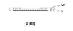
請參閱第9A圖至第9C圖,本案第四實施例與第一實施例大致相同,不同之處在於翻轉對位製程以及晶圓接合製程不同。由於第一基板1a與第二基板1i的熱傳導差異大,加上晶圓接合製程易有熱應力及氣泡(Void)等問題發生,因此,先成形第一基板1a、腔體層1b、振動層1c、第一金屬層1d、壓電致動層1e、隔離層1f、第二金屬層1g、防水層1h、第二光阻層M2以及共振層1m成為一單顆半成品後,再另外於入口層1k上進行滾壓及顯影製程成形流道層M3,最後翻轉入口層1k及流道層M3以覆晶(Flip Chip)方式與前述單顆半成品進行光學雙面對位完成接合。此外,為了減少第一基板1a經過蝕刻製程後產生脆裂的可能,可先於接合表面進行活性處理,藉此降低熱壓時的壓力。於本案第四實施例中,入口層1k為一電鑄或不銹鋼材質,藉以增加入口層1k之剛性,但不以此為限。Please refer to FIGS. 9A to 9C. The fourth embodiment of this case is substantially the same as the first embodiment, the difference is that the flip alignment process and the wafer bonding process are different. Since the difference in thermal conductivity between the
本案提供一微流體致動器,主要以微機電製程來完成的微流體致動器,並且藉由施加不同相位電荷之驅動電源於上電極焊墊以及下電極焊墊,使得振動層之振動區產生上下位移,進而達到流體傳輸。此外,藉由貼覆一陣裂孔片於出流孔洞上,作為一單向閥,避免流體回流現象發生,極具產業之利用價值,爰依法提出申請。This case provides a microfluidic actuator, a microfluidic actuator mainly completed by a micro-electromechanical process, and by applying driving power of different phase charges to the upper electrode pad and the lower electrode pad, the vibration area of the vibration layer is made Produce up and down displacement, and then achieve fluid transmission. In addition, by attaching a burst of holes to the outflow hole, it acts as a one-way valve to avoid the occurrence of fluid backflow and has great industrial use value. You have to apply according to law.
本案得由熟知此技術之人士任施匠思而為諸般修飾,然皆不脫如附申請專利範圍所欲保護者。This case must be modified by anyone familiar with this technology, such as Shi Jiangsi, but none of them are as protected as the scope of the patent application.
100、100'、100"、100'":微流體致動器100, 100', 100", 100'": microfluidic actuator
10:致動單元10: Actuating unit
1a、1a'":第一基板1a, 1a'": the first substrate
11a:第一表面11a: first surface
12a:第二表面12a: second surface
13a:出口溝槽13a: exit groove
14a:輔助溝槽14a: auxiliary groove
15a、15a'":第一出流孔洞15a, 15a'": the first outflow hole
16a、16a'":第二出流孔洞16a, 16a'": the second outflow hole
1b:腔體層1b: cavity layer
1c:振動層1c: Vibration layer
11c:流體溝槽11c: fluid groove
12c:振動區12c: Vibration zone
1d:第一金屬層1d: first metal layer
11d:下電極區11d: Lower electrode area
12d:阻障區12d: Obstacle zone
13d:間隙13d: clearance
1e:壓電致動層1e: piezoelectric actuation layer
11e:作動區11e: Action area
1f:隔離層1f: isolation layer
11f:間隙壁11f: spacer
1g:第二金屬層1g: second metal layer
11g:焊墊隔離區11g: pad isolation area
12g:上電極區12g: upper electrode area
13g:上電極焊墊13g: upper electrode pad
14g:下電極焊墊14g: Lower electrode pad
1h:防水層1h: waterproof layer
1i:第二基板1i: second substrate
1j:薄膜膠層1j: film adhesive layer
1k:入口層1k: entrance floor
1m:共振層1m: resonance layer
11m:腔體通孔11m: cavity through hole
12m:可動部12m: movable part
13m:固定部13m: fixed part
1n:罩幕層1n: mask layer
11n:罩幕開口11n: mask opening
12n:罩幕孔洞12n: Cover hole
13n:第一罩幕通孔13n: the first cover curtain through hole
14n:第二罩幕通孔14n: through hole of the second cover
1o、1o'":陣列孔片1o, 1o'": Array holes
11o:孔片孔洞11o: Hole hole
12o、12o'":定位孔12o, 12o'": positioning hole
13o'":支架部13o'": Support Department
AM1:第一接合對位記號AM1: first engagement registration mark
AM2:第二接合對位記號AM2: second engagement registration mark
AW:接合對位記號窗AW: Join the registration mark window
C1:入流腔室C1: Inflow chamber
C2:共振腔室C2: Resonance chamber
C3:儲流腔室C3: storage chamber
I:流體入口I: fluid inlet
M1:第一光阻層M1: the first photoresist layer
M1a:第一光阻區M1a: first photoresist area
M2:第二光阻層M2: second photoresist layer
M2a:第二光阻孔洞M2a: Second photoresist hole
M2b:第二光阻開口M2b: second photoresist opening
M3:流道層M3: flow channel layer
M31:流道入口M31: flow channel entrance
M32:腔體開口M32: cavity opening
M33:入流通道M33: Inflow channel
M4:第三光阻層M4: third photoresist layer
M41:第三光阻開口M41: third photoresist opening
P、P'":定位柱P, P'": Positioning column
第1A圖為本案微流體致動器之第一實施例之正面剖面示意圖。 第1B圖為本案第一實施例之側面剖面示意圖。 第2A圖至第2AH圖為本案第一實施例之製造步驟分解示意圖。 第3圖為本案第一實施例之俯視示意圖。 第4圖為本案第一實施例之入口層之俯視示意圖。 第5圖為本案第一實施例之流通孔之俯視示意圖。 第6A圖至第6E圖為本案第一實施例之作動示意圖。 第7A圖為本案微流體致動器之第二實施例之剖面示意圖。 第7B圖為本案其他實施例之仰視示意圖。 第8圖為本案第三實施例之陣列孔片之仰視示意圖。 第9A圖至第9C圖為本案第四實施例之翻轉對位製程以及晶圓接合製程示意圖。FIG. 1A is a schematic front cross-sectional view of the first embodiment of the microfluidic actuator of this case. FIG. 1B is a schematic side sectional view of the first embodiment of this case. Figures 2A to 2AH are exploded schematic views of the manufacturing steps of the first embodiment of the present invention. FIG. 3 is a schematic top view of the first embodiment of this case. Figure 4 is a schematic top view of the entrance layer of the first embodiment of the present invention. Fig. 5 is a schematic top view of the circulation hole of the first embodiment of the present invention. Figures 6A to 6E are schematic diagrams of the first embodiment of this case. FIG. 7A is a schematic cross-sectional view of a second embodiment of the microfluidic actuator of this case. FIG. 7B is a schematic diagram of looking up from other embodiments of the present case. FIG. 8 is a schematic bottom view of the array orifice of the third embodiment of the present invention. FIGS. 9A to 9C are schematic diagrams of the flip alignment process and the wafer bonding process of the fourth embodiment of the present invention.
100:微流體致動器100: Microfluidic actuator
10:致動單元10: Actuating unit
1a:第一基板1a: the first substrate
11 a:第一表面11 a: first surface
12 a:第二表面12 a: second surface
13a:出口溝槽13a: exit groove
14a:輔助溝槽14a: auxiliary groove
15a:第一出流孔洞15a: First outflow hole
16a:第二出流孔洞16a: Second outflow hole
1b:腔體層1b: cavity layer
1c:振動層1c: Vibration layer
12 c:振動區12 c: vibration zone
1d:第一金屬層1d: first metal layer
11 d:下電極區11 d: Lower electrode area
12 d:阻障區12 d: obstacle zone
1e:壓電致動層1e: piezoelectric actuation layer
11 e:作動區11 e: action area
1f:隔離層1f: isolation layer
11 f:間隙壁11 f: spacer
1g:第二金屬層1g: second metal layer
13g:上電極焊墊13g: upper electrode pad
14g:下電極焊墊14g: Lower electrode pad
1h:防水層1h: waterproof layer
1k:入口層1k: entrance floor
1m:共振層1m: resonance layer
11m:腔體通孔11m: cavity through hole
12m:可動部12m: movable part
13m:固定部13m: fixed part
1o:陣列孔片1o: Array hole piece
11o:孔片孔洞11o: Hole hole
C1:入流腔室C1: Inflow chamber
C2:共振腔室C2: Resonance chamber
C3:儲流腔室C3: storage chamber
I:流體入口I: fluid inlet
M2:第二光阻層M2: second photoresist layer
M3:第三光阻層M3: third photoresist layer
P:定位柱P: Positioning column
Claims (23)
Translated fromChinesePriority Applications (2)
| Application Number | Priority Date | Filing Date | Title |
|---|---|---|---|
| TW108101560ATWI695120B (en) | 2019-01-15 | 2019-01-15 | Micro fluid actuator |
| US16/740,839US11085554B2 (en) | 2019-01-15 | 2020-01-13 | Micro fluid actuator |
Applications Claiming Priority (1)
| Application Number | Priority Date | Filing Date | Title |
|---|---|---|---|
| TW108101560ATWI695120B (en) | 2019-01-15 | 2019-01-15 | Micro fluid actuator |
Publications (2)
| Publication Number | Publication Date |
|---|---|
| TWI695120Btrue TWI695120B (en) | 2020-06-01 |
| TW202028608A TW202028608A (en) | 2020-08-01 |
Family
ID=71517222
Family Applications (1)
| Application Number | Title | Priority Date | Filing Date |
|---|---|---|---|
| TW108101560ATWI695120B (en) | 2019-01-15 | 2019-01-15 | Micro fluid actuator |
Country Status (2)
| Country | Link |
|---|---|
| US (1) | US11085554B2 (en) |
| TW (1) | TWI695120B (en) |
Families Citing this family (6)
| Publication number | Priority date | Publication date | Assignee | Title |
|---|---|---|---|---|
| TWI741581B (en)* | 2020-04-30 | 2021-10-01 | 研能科技股份有限公司 | Heterogeneous integration chip of micro fluid actuator |
| TW202217146A (en)* | 2020-10-20 | 2022-05-01 | 研能科技股份有限公司 | Thin profile gas transporting device |
| US11940502B2 (en) | 2021-09-24 | 2024-03-26 | Analog Devices International Unlimited Company | Magnetic field sensing based on particle position within container |
| WO2023046901A1 (en) | 2021-09-24 | 2023-03-30 | Analog Devices International Unlimited Company, | Magnetic field sensing based on particle position within container |
| US12435803B2 (en) | 2022-05-27 | 2025-10-07 | Analog Devices International Unlimited Company | Flow adjustment based on particle movement in response to magnetic field |
| US12379433B2 (en) | 2022-09-14 | 2025-08-05 | Analog Devices International Unlimited Company | Magnetically sensitive particles and magnetic structure |
Citations (7)
| Publication number | Priority date | Publication date | Assignee | Title |
|---|---|---|---|---|
| US4826131A (en)* | 1988-08-22 | 1989-05-02 | Ford Motor Company | Electrically controllable valve etched from silicon substrates |
| JP2010064260A (en)* | 2008-09-08 | 2010-03-25 | Ricoh Co Ltd | Liquid ejection head and method for manufacturing the same, image forming apparatus |
| CN102979705A (en)* | 2011-09-06 | 2013-03-20 | 株式会社村田制作所 | Fluid control device |
| CN106926582A (en)* | 2015-12-29 | 2017-07-07 | 意法半导体股份有限公司 | Improved manufacturing method for fluid ejection device and fluid ejection device |
| TW201823145A (en)* | 2016-12-21 | 2018-07-01 | 日商精工愛普生股份有限公司 | Mems device, liquid jetting head, liquid jetting device, mems device manufacturing method, liquid jetting head manufacturing method, and liquid jetting device manufacturing method |
| GB2561925A (en)* | 2017-04-28 | 2018-10-31 | Cirrus Logic Int Semiconductor Ltd | MEMS devices and processes |
| TWM580642U (en)* | 2019-01-15 | 2019-07-11 | 研能科技股份有限公司 | Miniature fluid actuator |
Family Cites Families (1)
| Publication number | Priority date | Publication date | Assignee | Title |
|---|---|---|---|---|
| CN205260908U (en)* | 2013-05-24 | 2016-05-25 | 株式会社村田制作所 | Valve, fluid control device |
- 2019
- 2019-01-15TWTW108101560Apatent/TWI695120B/enactive
- 2020
- 2020-01-13USUS16/740,839patent/US11085554B2/enactiveActive
Patent Citations (7)
| Publication number | Priority date | Publication date | Assignee | Title |
|---|---|---|---|---|
| US4826131A (en)* | 1988-08-22 | 1989-05-02 | Ford Motor Company | Electrically controllable valve etched from silicon substrates |
| JP2010064260A (en)* | 2008-09-08 | 2010-03-25 | Ricoh Co Ltd | Liquid ejection head and method for manufacturing the same, image forming apparatus |
| CN102979705A (en)* | 2011-09-06 | 2013-03-20 | 株式会社村田制作所 | Fluid control device |
| CN106926582A (en)* | 2015-12-29 | 2017-07-07 | 意法半导体股份有限公司 | Improved manufacturing method for fluid ejection device and fluid ejection device |
| TW201823145A (en)* | 2016-12-21 | 2018-07-01 | 日商精工愛普生股份有限公司 | Mems device, liquid jetting head, liquid jetting device, mems device manufacturing method, liquid jetting head manufacturing method, and liquid jetting device manufacturing method |
| GB2561925A (en)* | 2017-04-28 | 2018-10-31 | Cirrus Logic Int Semiconductor Ltd | MEMS devices and processes |
| TWM580642U (en)* | 2019-01-15 | 2019-07-11 | 研能科技股份有限公司 | Miniature fluid actuator |
Also Published As
| Publication number | Publication date |
|---|---|
| US20200224791A1 (en) | 2020-07-16 |
| US11085554B2 (en) | 2021-08-10 |
| TW202028608A (en) | 2020-08-01 |
Similar Documents
| Publication | Publication Date | Title |
|---|---|---|
| TWI695120B (en) | Micro fluid actuator | |
| KR101153613B1 (en) | Micro-ejector and method for manufacturing the same | |
| CN209940465U (en) | Microfluidic actuator | |
| JP2011161915A (en) | Method for processing silicon substrate | |
| CN209583627U (en) | microfluidic actuator | |
| CN209098182U (en) | Microfluidic actuator | |
| TWM580642U (en) | Miniature fluid actuator | |
| KR100763907B1 (en) | Manufacturing method of microfluidic device and microfluidic device manufactured thereby | |
| TW202019808A (en) | Manufacturing method of micro fluid actuator | |
| TWM582072U (en) | Microfluidic actuator module | |
| TWI707487B (en) | Manufacturing method of micro fluid actuator | |
| TWI713142B (en) | Manufacturing method of miniature fluid actuator | |
| CN111434603B (en) | Microfluidic Actuators | |
| CN111750142B (en) | Microfluidic actuator module | |
| CN111434386B (en) | Fabrication method of microfluidic actuator | |
| CN111217317B (en) | Method for manufacturing microfluidic actuator | |
| TWI678819B (en) | Manufacturing method of micro fluid actuator | |
| TWI683462B (en) | Manufacturing method of micro fluid actuator module | |
| TWM576620U (en) | Miniature fluid actuator | |
| CN210003874U (en) | Microfluidic actuator module | |
| CN111254390B (en) | Method for manufacturing micro-fluid actuator | |
| TWI710517B (en) | Micro fluid actuator | |
| CN111252727B (en) | Microfluidic Actuators | |
| KR101208303B1 (en) | Micro-ejector and method for manufacturing the same | |
| CN112808330B (en) | Fabrication method of microfluidic actuator |