TWI692889B - Resistive random access memory structure and manufacturing method thereof - Google Patents
Resistive random access memory structure and manufacturing method thereofDownload PDFInfo
- Publication number
- TWI692889B TWI692889BTW108111859ATW108111859ATWI692889BTW I692889 BTWI692889 BTW I692889BTW 108111859 ATW108111859 ATW 108111859ATW 108111859 ATW108111859 ATW 108111859ATW I692889 BTWI692889 BTW I692889B
- Authority
- TW
- Taiwan
- Prior art keywords
- layer
- dielectric layer
- dielectric constant
- buffer layer
- random access
- Prior art date
Links
- 238000004519manufacturing processMethods0.000titleclaimsabstractdescription31
- 239000000463materialSubstances0.000claimsabstractdescription68
- 230000002093peripheral effectEffects0.000claimsabstractdescription42
- 239000000758substrateSubstances0.000claimsabstractdescription41
- 239000010410layerSubstances0.000claimsdescription341
- 238000005530etchingMethods0.000claimsdescription71
- 238000000034methodMethods0.000claimsdescription64
- 230000008569processEffects0.000claimsdescription54
- 239000011241protective layerSubstances0.000claimsdescription23
- 239000004020conductorSubstances0.000claimsdescription17
- XUIMIQQOPSSXEZ-UHFFFAOYSA-NSiliconChemical compound[Si]XUIMIQQOPSSXEZ-UHFFFAOYSA-N0.000claimsdescription7
- 229910052710siliconInorganic materials0.000claimsdescription7
- 239000010703siliconSubstances0.000claimsdescription7
- 229910052581Si3N4Inorganic materials0.000claimsdescription6
- HQVNEWCFYHHQES-UHFFFAOYSA-Nsilicon nitrideChemical compoundN12[Si]34N5[Si]62N3[Si]51N64HQVNEWCFYHHQES-UHFFFAOYSA-N0.000claimsdescription6
- 238000000151depositionMethods0.000claims2
- 239000003989dielectric materialSubstances0.000description13
- 230000007704transitionEffects0.000description10
- 238000005498polishingMethods0.000description8
- 238000007517polishing processMethods0.000description8
- 239000000126substanceSubstances0.000description8
- 229910052751metalInorganic materials0.000description7
- 239000002184metalSubstances0.000description7
- 239000002356single layerSubstances0.000description6
- 229910052721tungstenInorganic materials0.000description6
- 239000010937tungstenSubstances0.000description6
- RYGMFSIKBFXOCR-UHFFFAOYSA-NCopperChemical compound[Cu]RYGMFSIKBFXOCR-UHFFFAOYSA-N0.000description5
- UFHFLCQGNIYNRP-UHFFFAOYSA-NHydrogenChemical compound[H][H]UFHFLCQGNIYNRP-UHFFFAOYSA-N0.000description5
- NRTOMJZYCJJWKI-UHFFFAOYSA-NTitanium nitrideChemical compound[Ti]#NNRTOMJZYCJJWKI-UHFFFAOYSA-N0.000description5
- 229910052802copperInorganic materials0.000description5
- 239000010949copperSubstances0.000description5
- 239000001257hydrogenSubstances0.000description5
- 229910052739hydrogenInorganic materials0.000description5
- 125000006850spacer groupChemical group0.000description5
- RTAQQCXQSZGOHL-UHFFFAOYSA-NTitaniumChemical compound[Ti]RTAQQCXQSZGOHL-UHFFFAOYSA-N0.000description4
- 230000004888barrier functionEffects0.000description4
- 239000007772electrode materialSubstances0.000description4
- TWNQGVIAIRXVLR-UHFFFAOYSA-Noxo(oxoalumanyloxy)alumaneChemical compoundO=[Al]O[Al]=OTWNQGVIAIRXVLR-UHFFFAOYSA-N0.000description4
- 239000004065semiconductorSubstances0.000description4
- 239000010936titaniumSubstances0.000description4
- 229910052719titaniumInorganic materials0.000description4
- WFKWXMTUELFFGS-UHFFFAOYSA-NtungstenChemical compound[W]WFKWXMTUELFFGS-UHFFFAOYSA-N0.000description4
- VYPSYNLAJGMNEJ-UHFFFAOYSA-NSilicium dioxideChemical groupO=[Si]=OVYPSYNLAJGMNEJ-UHFFFAOYSA-N0.000description3
- 229910052782aluminiumInorganic materials0.000description3
- XAGFODPZIPBFFR-UHFFFAOYSA-NaluminiumChemical compound[Al]XAGFODPZIPBFFR-UHFFFAOYSA-N0.000description3
- 238000005229chemical vapour depositionMethods0.000description3
- 239000010432diamondSubstances0.000description3
- 150000002739metalsChemical class0.000description3
- 238000000059patterningMethods0.000description3
- 229920003209poly(hydridosilsesquioxane)Polymers0.000description3
- 229910052814silicon oxideInorganic materials0.000description3
- 229910052715tantalumInorganic materials0.000description3
- GUVRBAGPIYLISA-UHFFFAOYSA-Ntantalum atomChemical compound[Ta]GUVRBAGPIYLISA-UHFFFAOYSA-N0.000description3
- MZLGASXMSKOWSE-UHFFFAOYSA-Ntantalum nitrideChemical compound[Ta]#NMZLGASXMSKOWSE-UHFFFAOYSA-N0.000description3
- -1tungsten nitrideChemical class0.000description3
- BOTDANWDWHJENH-UHFFFAOYSA-NTetraethyl orthosilicateChemical compoundCCO[Si](OCC)(OCC)OCCBOTDANWDWHJENH-UHFFFAOYSA-N0.000description2
- 125000004429atomChemical group0.000description2
- 238000000231atomic layer depositionMethods0.000description2
- 238000005137deposition processMethods0.000description2
- 229910052735hafniumInorganic materials0.000description2
- VBJZVLUMGGDVMO-UHFFFAOYSA-Nhafnium atomChemical compound[Hf]VBJZVLUMGGDVMO-UHFFFAOYSA-N0.000description2
- 229910000449hafnium oxideInorganic materials0.000description2
- WIHZLLGSGQNAGK-UHFFFAOYSA-Nhafnium(4+);oxygen(2-)Chemical compound[O-2].[O-2].[Hf+4]WIHZLLGSGQNAGK-UHFFFAOYSA-N0.000description2
- 239000007769metal materialSubstances0.000description2
- 150000004767nitridesChemical class0.000description2
- 229910018072Al 2 O 3Inorganic materials0.000description1
- 150000001875compoundsChemical class0.000description1
- 238000005336crackingMethods0.000description1
- 230000006866deteriorationEffects0.000description1
- 230000008020evaporationEffects0.000description1
- 238000001704evaporationMethods0.000description1
- CJNBYAVZURUTKZ-UHFFFAOYSA-Nhafnium(iv) oxideChemical compoundO=[Hf]=OCJNBYAVZURUTKZ-UHFFFAOYSA-N0.000description1
- 150000002431hydrogenChemical class0.000description1
- 239000012212insulatorSubstances0.000description1
- 229910044991metal oxideInorganic materials0.000description1
- 150000004706metal oxidesChemical class0.000description1
- 125000005429oxyalkyl groupChemical group0.000description1
- BPUBBGLMJRNUCC-UHFFFAOYSA-Noxygen(2-);tantalum(5+)Chemical compound[O-2].[O-2].[O-2].[O-2].[O-2].[Ta+5].[Ta+5]BPUBBGLMJRNUCC-UHFFFAOYSA-N0.000description1
- RVTZCBVAJQQJTK-UHFFFAOYSA-Noxygen(2-);zirconium(4+)Chemical compound[O-2].[O-2].[Zr+4]RVTZCBVAJQQJTK-UHFFFAOYSA-N0.000description1
- 238000005240physical vapour depositionMethods0.000description1
- 239000005368silicate glassSubstances0.000description1
- 150000004760silicatesChemical class0.000description1
- 238000004544sputter depositionMethods0.000description1
- 229910000314transition metal oxideInorganic materials0.000description1
- 229910001928zirconium oxideInorganic materials0.000description1
Images


Classifications
- H—ELECTRICITY
- H10—SEMICONDUCTOR DEVICES; ELECTRIC SOLID-STATE DEVICES NOT OTHERWISE PROVIDED FOR
- H10B—ELECTRONIC MEMORY DEVICES
- H10B63/00—Resistance change memory devices, e.g. resistive RAM [ReRAM] devices
- H10B63/80—Arrangements comprising multiple bistable or multi-stable switching components of the same type on a plane parallel to the substrate, e.g. cross-point arrays
- H—ELECTRICITY
- H10—SEMICONDUCTOR DEVICES; ELECTRIC SOLID-STATE DEVICES NOT OTHERWISE PROVIDED FOR
- H10N—ELECTRIC SOLID-STATE DEVICES NOT OTHERWISE PROVIDED FOR
- H10N70/00—Solid-state devices having no potential barriers, and specially adapted for rectifying, amplifying, oscillating or switching
- H10N70/801—Constructional details of multistable switching devices
- H10N70/841—Electrodes
- H—ELECTRICITY
- H10—SEMICONDUCTOR DEVICES; ELECTRIC SOLID-STATE DEVICES NOT OTHERWISE PROVIDED FOR
- H10N—ELECTRIC SOLID-STATE DEVICES NOT OTHERWISE PROVIDED FOR
- H10N70/00—Solid-state devices having no potential barriers, and specially adapted for rectifying, amplifying, oscillating or switching
- H10N70/801—Constructional details of multistable switching devices
- H10N70/881—Switching materials
- H10N70/883—Oxides or nitrides
- G—PHYSICS
- G11—INFORMATION STORAGE
- G11C—STATIC STORES
- G11C13/00—Digital stores characterised by the use of storage elements not covered by groups G11C11/00, G11C23/00, or G11C25/00
- G11C13/0002—Digital stores characterised by the use of storage elements not covered by groups G11C11/00, G11C23/00, or G11C25/00 using resistive RAM [RRAM] elements
- G11C13/0007—Digital stores characterised by the use of storage elements not covered by groups G11C11/00, G11C23/00, or G11C25/00 using resistive RAM [RRAM] elements comprising metal oxide memory material, e.g. perovskites
- H—ELECTRICITY
- H10—SEMICONDUCTOR DEVICES; ELECTRIC SOLID-STATE DEVICES NOT OTHERWISE PROVIDED FOR
- H10N—ELECTRIC SOLID-STATE DEVICES NOT OTHERWISE PROVIDED FOR
- H10N70/00—Solid-state devices having no potential barriers, and specially adapted for rectifying, amplifying, oscillating or switching
- H10N70/011—Manufacture or treatment of multistable switching devices
- H—ELECTRICITY
- H10—SEMICONDUCTOR DEVICES; ELECTRIC SOLID-STATE DEVICES NOT OTHERWISE PROVIDED FOR
- H10N—ELECTRIC SOLID-STATE DEVICES NOT OTHERWISE PROVIDED FOR
- H10N70/00—Solid-state devices having no potential barriers, and specially adapted for rectifying, amplifying, oscillating or switching
- H10N70/20—Multistable switching devices, e.g. memristors
- H—ELECTRICITY
- H10—SEMICONDUCTOR DEVICES; ELECTRIC SOLID-STATE DEVICES NOT OTHERWISE PROVIDED FOR
- H10N—ELECTRIC SOLID-STATE DEVICES NOT OTHERWISE PROVIDED FOR
- H10N70/00—Solid-state devices having no potential barriers, and specially adapted for rectifying, amplifying, oscillating or switching
- H10N70/801—Constructional details of multistable switching devices
- H10N70/821—Device geometry
- H10N70/826—Device geometry adapted for essentially vertical current flow, e.g. sandwich or pillar type devices
- H—ELECTRICITY
- H10—SEMICONDUCTOR DEVICES; ELECTRIC SOLID-STATE DEVICES NOT OTHERWISE PROVIDED FOR
- H10N—ELECTRIC SOLID-STATE DEVICES NOT OTHERWISE PROVIDED FOR
- H10N70/00—Solid-state devices having no potential barriers, and specially adapted for rectifying, amplifying, oscillating or switching
- H10N70/801—Constructional details of multistable switching devices
- H10N70/881—Switching materials
- H10N70/883—Oxides or nitrides
- H10N70/8833—Binary metal oxides, e.g. TaOx
Landscapes
- Chemical & Material Sciences (AREA)
- Engineering & Computer Science (AREA)
- Materials Engineering (AREA)
- Semiconductor Memories (AREA)
Abstract
Description
Translated fromChinese本發明係有關於一種記憶體裝置,且特別係有關於一種電阻式隨機存取記憶體結構及其製造方法。The present invention relates to a memory device, and particularly relates to a resistive random access memory structure and a manufacturing method thereof.
電阻式隨機存取記憶體(RRAM)具有結構簡單、面積小、操作電壓小、操作速度快、記憶時間長、多狀態記憶、及耗功率低等優點。因此電阻式隨機存取記憶體極有潛力取代目前的快閃式記憶體,成為下世代的非揮發性記憶體主流。Resistive random access memory (RRAM) has the advantages of simple structure, small area, small operating voltage, fast operating speed, long memory time, multi-state memory, and low power consumption. Therefore, resistive random access memory has great potential to replace the current flash memory and become the mainstream of the next generation of non-volatile memory.
在習知的電阻式隨機存取記憶體中,一個晶片通常包括陣列區與周邊區。陣列區包括多個記憶體單元,且每個記憶體單元包括圖案化的底電極層、電阻轉態層與頂電極層。周邊區主要是邏輯電路。在周邊區中,為了提高邏輯電路的操作速度,介電層通常會使用低介電常數(low-k)介電材料。然而,由於低介電常數介電材料的間隙填充能力不佳且記憶體單元之間的空間很小,若採用低介電常數介電材料填充於陣列區的間隙,將導致這些記憶體單元之間產生孔洞。如此一來,電阻式隨機存取記憶體裝置的操作容易出錯,且產品的良率及可靠度皆變差。In the conventional resistance random access memory, a chip usually includes an array area and a peripheral area. The array area includes a plurality of memory cells, and each memory cell includes a patterned bottom electrode layer, a resistance transition layer, and a top electrode layer. The surrounding area is mainly logic circuits. In the peripheral area, in order to increase the operating speed of the logic circuit, a low-k dielectric material is usually used for the dielectric layer. However, due to the poor gap filling ability of low dielectric constant dielectric materials and the small space between memory cells, if low dielectric constant dielectric materials are used to fill the gaps in the array area, these memory cells There are holes between them. As a result, the operation of the resistive random access memory device is error-prone, and the yield and reliability of the product are deteriorated.
再者,當進行蝕刻製程形成定義導電插塞的開口時,陣列區與周邊區需要的開口深度不同。若採用相同條件形成陣列區與周邊區的上述開口,則可能導致記憶體單元被過度蝕刻而受到損傷,進而降低電阻式隨機存取記憶體的可靠度與良率。另一方面,若在不同的蝕刻步驟中分別形成陣列區與周邊區的上述開口,則製程的複雜度、生產成本及生產時間皆會大幅增加。Furthermore, when an etching process is performed to form an opening defining a conductive plug, the opening depth required by the array region and the peripheral region is different. If the openings in the array area and the peripheral area are formed under the same conditions, the memory cell may be over-etched and damaged, thereby reducing the reliability and yield of the resistive random access memory. On the other hand, if the above-mentioned openings of the array area and the peripheral area are formed in different etching steps, the complexity of the manufacturing process, the production cost, and the production time will be greatly increased.
對記憶體產業的業者而言,為了提升電阻式隨機存取記憶體的可靠度與產品良率,並且降低生產所需的成本及時間,仍有需要對電阻式隨機存取記憶體及其製程進行改良。For the memory industry, in order to improve the reliability and product yield of resistive random access memory, and reduce the cost and time required for production, there is still a need for resistive random access memory and its manufacturing process Make improvements.
本發明實施例提供一種電阻式隨機存取記憶體結構及其製造方法,能夠明顯改善產品的良率及可靠度,並且降低製程的複雜度、生產成本及生產時間。Embodiments of the present invention provide a resistive random access memory structure and a manufacturing method thereof, which can significantly improve the yield and reliability of products, and reduce the complexity of the manufacturing process, production cost, and production time.
本發明之一實施例係揭示一種電阻式隨機存取記憶體結構,包括:基板,其中基板包括陣列區及周邊區;複數個記憶體單元,位於基板上且位於陣列區中;間隙填充介電層,位於陣列區中且覆蓋記憶體單元;緩衝層,覆蓋間隙填充介電層,其中緩衝層只位於陣列區中,且緩衝層的材料不同於間隙填充介電層的材料;第一低介電常數介電層,只位於周邊區中,其中第一低介電常數介電層的材料不同於緩衝層的材料,第一低介電常數介電層的介電常數小於3,且第一低介電常數介電層的頂表面與緩衝層的頂表面共平面;以及第一導電插塞,穿過緩衝層及間隙填充介電層,且與記憶體單元之中的一者接觸。An embodiment of the present invention discloses a resistive random access memory structure, including: a substrate, wherein the substrate includes an array area and a peripheral area; a plurality of memory cells are located on the substrate and in the array area; gap-fill dielectric Layer, located in the array area and covering the memory cell; buffer layer, covering the gap filling dielectric layer, wherein the buffer layer is only located in the array area, and the material of the buffer layer is different from the material of the gap filling dielectric layer; the first low dielectric The dielectric constant dielectric layer is only located in the peripheral area, wherein the material of the first low dielectric constant dielectric layer is different from the material of the buffer layer, the dielectric constant of the first low dielectric constant dielectric layer is less than 3, and the first The top surface of the low dielectric constant dielectric layer is coplanar with the top surface of the buffer layer; and the first conductive plug fills the dielectric layer through the buffer layer and the gap, and contacts one of the memory cells.
本發明之一實施例係揭示一種電阻式隨機存取記憶體結構的製造方法,包括:提供基板,其中基板包括陣列區及周邊區;形成複數個記憶體單元於基板上且位於陣列區中;形成間隙填充介電層於陣列區中且覆蓋記憶體單元;形成緩衝層覆蓋間隙填充介電層,其中緩衝層只位於陣列區中,且緩衝層的材料不同於間隙填充介電層的材料;形成第一低介電常數介電層只位於周邊區中,其中第一低介電常數介電層的材料不同於緩衝層的材料,第一低介電常數介電層的介電常數小於3,且第一低介電常數介電層的頂表面與緩衝層的頂表面共平面;以及形成第一導電插塞,其中第一導電插塞延伸穿過緩衝層及間隙填充介電層,且與記憶體單元之中的一者接觸。An embodiment of the present invention discloses a method for manufacturing a resistive random access memory structure, including: providing a substrate, wherein the substrate includes an array area and a peripheral area; forming a plurality of memory cells on the substrate and located in the array area; Forming a gap-fill dielectric layer in the array area and covering the memory cell; forming a buffer layer to cover the gap-fill dielectric layer, wherein the buffer layer is only located in the array area, and the material of the buffer layer is different from the material of the gap-fill dielectric layer; The first low dielectric constant dielectric layer is formed only in the peripheral region, wherein the material of the first low dielectric constant dielectric layer is different from the material of the buffer layer, and the dielectric constant of the first low dielectric constant dielectric layer is less than 3 And the top surface of the first low dielectric constant dielectric layer is coplanar with the top surface of the buffer layer; and a first conductive plug is formed, wherein the first conductive plug extends through the buffer layer and the gap fills the dielectric layer, and Contact with one of the memory cells.
在本發明實施例所提供之電阻式隨機存取記憶體結構中,形成一層緩衝層覆蓋整個陣列區,藉此可改善間隙填充介電層的機械強度。即使陣列區的間隙填充介電層與周邊區的介電層使用不同的介電材料,間隙填充介電層也不容易在化學機械研磨製程期間受到損傷。因此,可根據需求分別選擇陣列區與周邊區的介電材料。再者,在進行蝕刻製程時,緩衝層可保護位於陣列區的記憶體單元。因此,可在同一蝕刻製程中同時形成陣列區與周邊區的開口。如此一來,能夠明顯改善產品的良率及可靠度,而不會明顯增加製程的複雜度、生產成本及生產時間。In the resistive random access memory structure provided by the embodiment of the present invention, a buffer layer is formed to cover the entire array area, thereby improving the mechanical strength of the gap-filling dielectric layer. Even if different dielectric materials are used for the gap-fill dielectric layer of the array region and the dielectric layer of the peripheral region, the gap-fill dielectric layer is not easily damaged during the chemical mechanical polishing process. Therefore, the dielectric materials of the array area and the peripheral area can be selected according to requirements. Furthermore, during the etching process, the buffer layer can protect the memory cells located in the array area. Therefore, the openings of the array area and the peripheral area can be simultaneously formed in the same etching process. In this way, the yield and reliability of the product can be significantly improved without significantly increasing the complexity of the manufacturing process, production cost and production time.
為使本發明之目的、特徵、優點能更明顯易懂,下文特舉出較佳實施例,並配合所附圖式,作詳細說明如下。In order to make the purpose, features, and advantages of the present invention more obvious and understandable, the preferred embodiments are specifically described below, and in conjunction with the accompanying drawings, detailed descriptions are as follows.
於本文中,低介電常數介電材料的介電常數小於3。低介電常數介電層的材料可包括SiLKTM、低介電常數可流動氧化物(low k- flowable oxide, FOx)、氟化矽酸鹽玻璃(Fluorinated silicate glass, FSG)、氫矽倍半氧烷( hydrogen silsesquioxane, HSQ)、甲基矽倍半氧烷(methylsilsesquioxane, MSQ)、Nanoglass、Black DiamondTM、CoralTM、AuroraTM或其他已知的低介電常數介電材料。In this article, the dielectric constant of low dielectric constant dielectric materials is less than 3. The materials of the low dielectric constant dielectric layer may include SiLKTM , low k-flowable oxide (FOx), fluorinated silicate glass (FSG), hydrogen silicon halves Oxyalkyl (hydrogen silsesquioxane, HSQ), methylsilsesquioxane (MSQ), Nanoglass, Black Diamond™ , Coral™ , Aurora™ or other known low dielectric constant dielectric materials.
第1A圖至第1G圖為本發明一些實施例之電阻式隨機存取記憶體結構100的製造方法的各步驟中所對應的剖面示意圖。請參照第1A圖,提供基板102,且基板102包括陣列區10及周邊區20。接著,依序形成介電層104與第一保護層106於基板102上。基板102的材料可包括塊材半導體基板(例如,矽基板)、化合物半導體基板(例如,IIIA-VA族半導體基板)、絕緣層上覆矽(silicon on insulator, SOI)基板等。基板102可為經摻雜或未經摻雜的半導體基板。在一些實施例中,基板102為矽基板。介電層104的材料不同於第一保護層106的材料。在一些實施例中,介電層104可為低介電常數介電材料,例如,Black DiamondTM,且第一保護層106可為四乙氧基矽烷(TEOS)、氮化矽(SiN)或碳氮化矽(SiCN)。FIGS. 1A to 1G are schematic cross-sectional views corresponding to the steps of the method for manufacturing the resistive random
接著,對介電層104與第一保護層106進行圖案化製程,以形成開口。第一保護層106保護介電層104不受水氣以及後續蝕刻製程的影響。接著,將金屬材料填入開口中,並且藉由平坦化製程(例如,化學機械研磨製程)移除位於第一保護層106上的多餘的金屬材料,以形成接觸插塞108於介電層104與第一保護層106中。在一些實施例中接觸插塞108為單層結構,且包括鎢、鋁、銅、其他合適的金屬或上述之組合。在一些實施例中,接觸插塞108的材料為銅,因而接觸插塞108的導電性良好。在另一些實施例中,接觸插塞108的材料為鎢,因而可避免金屬原子擴散進入基板102或介電層104中。在本實施例中,接觸插塞108包括襯層108a及導電層108b。襯層108a可改善導電層108b與基板102或介電層104的黏著性,且可避免金屬原子擴散進入基板102或介電層104中。襯層108a的材料可包括鈦、氮化鈦、氮化鎢、鉭或氮化鉭、其他合適的導電材料或上述之組合。導電層108b的材料可包括鎢、鋁、銅、其他合適的金屬或上述之組合。Next, a patterning process is performed on the
接著,形成複數個記憶體單元110於位於陣列區10的基板102上。記憶體單元110的位置可對應於接觸插塞108的位置,從而與接觸插塞108電連接。在一些實施例中,在基板102與介電層104之間還配置有經圖案化的導線層(未繪示出),且接觸插塞108被配置以使經圖案化的導線層電性連接至記憶體單元110。各記憶體單元110可包括底電極層112、電阻轉態層114及頂電極層116。舉例而言,可藉由以下的方法形成記憶體單元110。首先,在第一保護層106上依序形成底電極材料、電阻轉態材料及頂電極材料。接著,圖案化底電極材料、電阻轉態材料及頂電極材料,以形成多個記憶體單元110於陣列區10中。Next, a plurality of
底電極層112可藉由接觸插塞108與其他元件(未繪示)電性連接。藉由對底電極層112與頂電極層116施加電壓,可將電阻轉態層114轉換成不同的電阻狀態。底電極層112的材料與頂電極層116的材料可各自獨立地包括鈦、鉭、氮化鈦、氮化鉭、其他合適的導電材料或上述之組合。底電極層112與頂電極層116可各自獨立地為由單一材料所形成的單層結構或由多種不同材料所形成的多層結構。在一些實施例中,底電極層112為由氮化鈦所形成的單層結構,且頂電極層116為由鈦所形成的單層結構。可各自獨立地利用物理氣相沉積製程、化學氣相沉積或其他合適的沉積製程,以形成底電極層112與頂電極層116。The
電阻轉態層114的材料可包括單層或多層的過渡金屬氧化物,例如,氧化鉭(Ta2O5)、氧化鉿(HfO2)、氧化鋁(Al2O3)、氧化鋯(ZrO2)或上述組合的疊層。在一些實施例中,電阻轉態層114的材料可為氧化鋁與氧化鉿組合的疊層。可利用合適的製程形成電阻轉態層114,例如,濺鍍製程、原子層沉積製程、化學氣相沉積製程、蒸鍍製程或其他合適的沉積製程。The material of the
接著,形成第二保護層120覆蓋陣列區10及周邊區20,且第二保護層120順應性地覆蓋記憶體單元110。第二保護層120可為由單一材料所形成的單層結構或由多種不同材料所形成的多層結構。在一些實施例中,第二保護層120為由氫氣阻障層及形成於氫氣阻障層上的間隔層所形成的雙層結構。在這樣的實施例中,氫氣阻障層可避免氫氣進入基板102中,因而可避免電阻式隨機存取記憶體結構的劣化或失效。氫氣阻障層的材料可為金屬氧化物(例如,氧化鋁)、金屬氮化物、金屬氮氮化物或上述之組合。間隔層可減少或避免記憶體單元110在後續製程中受到損傷。間隔層的材料可為氧化物、氮化物或氮氧化物。在本實施例中,間隔層的材料為氧化矽或氮化矽。在另一些實施例中,間隔層可省略。Next, a second
接著,形成間隙填充介電層122覆蓋陣列區10及周邊區20,且間隙填充介電層122覆蓋記憶體單元110。之後,進行平坦化製程,使間隙填充介電層122具有平坦的頂表面。由於間隙填充介電層122具有良好的間隙填充能力,可避免在陣列區10產生孔洞。如此一來,可減少或避免電阻式隨機存取記憶體結構的操作錯誤,且可明顯改善產品的良率及可靠度。間隙填充介電層122的材料可包括氧化物,例如,氧化矽、氧化鋁、氧化鉿、氮氧化鉿、氮氧矽化鉿等,且可藉由化學氣相沉積法或是原子層沉積形成。Next, a gap-
接著,形成緩衝層124覆蓋間隙填充介電層122。緩衝層124的材料可包括氮化矽或碳氮化矽。緩衝層124的材料與間隙填充介電層122的材料不同。於一實施例中,緩衝層124的材料不同於間隙填充介電層122及介電層104的材料。在本實施例中,緩衝層124的材料為氮化矽,間隙填充介電層122的材料為氧化矽。Next, a
請參照第1B圖,進行圖案化製程,以移除位於周邊區20的所有緩衝層124、間隙填充介電層122、第二保護層120及第一保護層106。接著,順應性地形成緩衝層124覆蓋陣列區10及周邊區20,使間隙填充介電層122的側壁上配置有緩衝層124。之後,移除位於周邊區20的緩衝層124。換言之,整個間隙填充介電層122受到緩衝層124的包覆,且形成於間隙填充介電層122的側壁上的緩衝層124作為陣列區10與周邊區20的交界。藉此,緩衝層124在間隙填充介電層122頂部的厚度大於在間隙填充介電層122側壁的厚度。Referring to FIG. 1B, a patterning process is performed to remove all the
請參照第1C圖,形成低介電常數介電材料覆蓋陣列區10及周邊區20。之後,進行化學機械研磨製程,以形成頂表面與緩衝層124的頂表面共平面的第一低介電常數介電層126。即,移除位於陣列區10的低介電常數介電材料。第一低介電常數介電層126的介電常數小於間隙填充介電層122,藉此可提高周邊區20的邏輯電路的操作速度。於本實施例中,通過將第一低介電常數介電層126局限於沒有記憶體單元110存在的周邊區20,即使第一低介電常數介電層126的間隙填充能力較差,也不會造成電阻式隨機存取記憶體結構的操作錯誤。在本實施例中,第一低介電常數介電層126的材料為Black diamondTM。第一低介電常數介電層126的材料與緩衝層124的材料不同。Referring to FIG. 1C, a low-k dielectric material is formed to cover the
請參照第1D圖,形成第二低介電常數介電層128於緩衝層124及第一低介電常數介電層126上。第二低介電常數介電層128的材料可與第一低介電常數介電層126的材料相同或相似。換言之,第二低介電常數介電層128的介電常數可小於3。如此一來,可提高邏輯電路及記憶體單元110的操作速度。Referring to FIG. 1D, a second low dielectric
請參照第1E圖,使用第一罩幕(未繪示)進行第一蝕刻製程,以形成第一開口125於陣列區10中,且形成深度大於第一開口125的深度的第二開口135於周邊區20中。第一開口125的位置可對應於記憶體單元110的位置。第一開口125穿過第二低介電常數介電層128及緩衝層124,而暴露出間隙填充介電層122。第二開口135穿過第二低介電常數介電層128及第一低介電常數介電層126,而暴露出介電層104。在本實施例中,第一蝕刻製程為非等向性的蝕刻製程。第一蝕刻製程移除了部分的介電層104。Referring to FIG. 1E, a first etching process is performed using a first mask (not shown) to form a
於第一蝕刻製程中,藉由採用對低介電常數介電材料具有較高選擇性的蝕刻條件,且以緩衝層124包覆間隙填充介電層122,第二開口135的深度容易地被配置地比第一開口125的深度大,使第一開口125的深度控制在暴露出間隙填充介電層122的位置。亦即,保證在第一蝕刻製程中不會傷害記憶體單元110。In the first etching process, by using an etching condition with higher selectivity for low dielectric constant dielectric materials, and filling the gap with the
請參照第1F圖,使用第二罩幕(未繪示)進行第二蝕刻製程。在第二蝕刻製程之後,在陣列區10中,第一開口125被加深而暴露出記憶體單元110的頂電極層116,且第一開口125的上部分被擴大而形成第一溝槽127於第二低介電常數介電層128中。在第二蝕刻製程之後,在陣列區20中,第二開口135被加深而暴露出基板102,且第二開口135的上部分被擴大而形成第二溝槽137於第二低介電常數介電層128中。在本實施例中,第二蝕刻製程為非等向性的蝕刻製程。Please refer to FIG. 1F to perform a second etching process using a second mask (not shown). After the second etching process, in the
請參照第1G圖,順應性地沉積導電襯層材料於第一開口125、第一溝槽127、第二開口135及第二溝槽137中,以在第一開口125的表面形成導電襯層130a,在第一溝槽127的表面形成導電襯層132a,在第二開口135的表面形成導電襯層140a,及在第二溝槽137的表面形成導電襯層142a。接著,以導電材料填滿第一開口125、第一溝槽127、第二開口135及第二溝槽137,以在導電襯層130a上形成導電材料層130b,在導電襯層132a上形成導電材料層132b,在導電襯層140a上形成導電材料層140b,及在導電襯層142a上形成導電材料層142b。如此一來,可形成第一導電插塞130於第一開口125、形成第一導電線路132於第一溝槽127、形成第二導電插塞140於第二開口135及形成第二導電線路142於第二溝槽137中。導電襯層材料可包括鈦、氮化鈦、氮化鎢、鉭或氮化鉭或上述之組合。導電材料可包括鎢、鋁、銅、其他合適的金屬或上述之組合。在本實施例中,導電襯層材料為氮化鈦,且導電材料為導電性良好的銅。因此,可提高邏輯電路及記憶體單元110的操作速度。之後,可進行其他習知的製程,以完成電阻式隨機存取記憶體結構100,在此不再詳述。Referring to FIG. 1G, a conductive liner material is compliantly deposited in the
在本實施例所提供之電阻式隨機存取記憶體結構100的製造方法中,緩衝層124覆蓋整個陣列區10。這樣的結構能夠明顯改善產品的良率及可靠度,而不會明顯增加製程的複雜度、生產成本及生產時間。In the manufacturing method of the resistive random
更詳言之,間隙填充介電層122的材料與第一低介電常數介電層126的材料具有不同的性質,例如,硬度與機械強度。在未形成緩衝層124的對照組中,當進行第1C圖所述的化學機械研磨製程時,研磨壓力可能會導致間隙填充介電層122與第一低介電常數介電層126的交界處破裂。如此一來,陣列區10的元件(例如記憶體單元110)或周邊區的元件(例如邏輯電路)將容易因後續製程而受到損傷。例如,後續製程的溶液(例如,研磨液或蝕刻溶液)可能會沿著裂縫滲入陣列區10或周邊區20,進而導致元件損壞。如此一來,會降低記憶體的良率與可靠度。在本實施例中,藉由形成緩衝層124覆蓋整個陣列區10,其中緩衝層124的材料不同於間隙填充介電層122的材料,且緩衝層124的機械強度優於間隙填充介電層122的機械強度。因此,緩衝層124可提供良好的支撐力,改善機械強度。如此一來,即使發生上述破裂的現象,陣列區10的元件仍受到緩衝層124的保護,進而改善產品的良率與可靠度。More specifically, the material of the gap-
在本實施例中,緩衝層124的材料不同於第一低介電常數介電層126的材料,且緩衝層124的研磨速率低於第一低介電常數介電層126的研磨速率。因此,在化學機械研磨製程中,緩衝層124可作為研磨停止層,以確保第一低介電常數介電層126的頂表面與緩衝層124的頂表面齊平。如此一來,第二低介電常數介電層128可具有平坦的頂表面,因而有助於改善產品的良率。在一些實施例中,在第1C圖所述的化學機械研磨製程期間,對第一低介電常數介電層126具有第一研磨速率PR1,對緩衝層124具有第二研磨速率PR2,且第一研磨速率PR1相對於第二研磨速率PR2的比例PR1/PR2為5-10。In this embodiment, the material of the
再者,在未形成緩衝層124的對照組中,於進行第1E圖所述的第一蝕刻製程時,當第一開口125已暴露出頂電極層116時,第二開口135仍未蝕刻到預定深度。如此一來,若繼續進行第一蝕刻製程以完成第二開口135,將使暴露的頂電極層116受到很大的傷害,造成可靠度與良率皆降低。在本實施例中,緩衝層124的材料不同於第一低介電常數介電層126的材料,且緩衝層124的蝕刻速率低於第一低介電常數介電層126的蝕刻速率。因此,容易地在第一蝕刻製程中形成深度較小的第一開口125及深度較大的第二開口135。在一些實施例中,在第1E圖所述的第一蝕刻製程期間,緩衝層124具有第一蝕刻速率R1,第一低介電常數介電層126具有第二蝕刻速率R2,且第二蝕刻速率R2相對於第一蝕刻速率R1的比例R2/R1為5-20。請參照第1E圖,在第一蝕刻製程之後,第二開口135穿過第一低介電常數介電層126,且第一開口125穿過緩衝層124。換言之,第一開口125的深度小於第二開口135的深度,且並未暴露頂電極層116。因此,可避免頂電極層116在第一蝕刻製程期間受到傷害。如此一來,可明顯改善記憶體的可靠度與良率。Furthermore, in the control group where the
另一方面,在第1F圖所述的第二蝕刻製程中,間隙填充介電層122的蝕刻速率與第二低介電常數介電層128的蝕刻速率是相近的。在未形成緩衝層124的對照組中,當進行第1F圖所述的第二蝕刻製程時,相鄰的第一開口125之間的距離可能會變得太近,而容易發生短路。因此,記憶體的良率會降低,且不利於記憶體裝置的微小化。在本實施例中,緩衝層124的材料不同於第二低介電常數介電層128的材料,且緩衝層124的蝕刻速率低於第二低介電常數介電層128的蝕刻速率。因此,可精準控制第一開口125的寬度與剖面輪廓。在一些實施例中,在第1F圖所述的第二蝕刻製程期間,緩衝層124具有第三蝕刻速率R3,第二低介電常數介電層128具有第四蝕刻速率R4,且第四蝕刻速率R4相對於該第三蝕刻速率R3的比例R4/R3為5-20。請參照第1F圖,在第二蝕刻製程之後,第一開口125的上部分具有實質均一的寬度,且與第一溝槽127的底表面的剖面輪廓實質上是水平的。因此,可改善電阻式隨機存取記憶體的良率,且有利於記憶體裝置的微小化。On the other hand, in the second etching process described in FIG. 1F, the etching rate of the gap-filling
請參照第1G圖,在一些實施例中,提供一種電阻式隨機存取記憶體結構100。電阻式隨機存取記憶體結構100包括具有陣列區10及周邊區20的基板102。在陣列區10中,複數個記憶體單元110、順應性地覆蓋記憶體單元110的第二保護層120及覆蓋第二保護層120的間隙填充介電層122位於基板102上。再者。緩衝層124只位於陣列區10中,且覆蓋整個間隙填充介電層122。緩衝層124的材料不同於間隙填充介電層122的材料。第一低介電常數介電層126位於基板102上,且只位於周邊區20中。第一低介電常數介電層126的頂表面與緩衝層124的頂表面共平面。第二低介電常數介電層128位於緩衝層124及第一低介電常數介電層126上。在陣列區10中,第一導電插塞130穿過緩衝層124及間隙填充介電層122,且與其中一個記憶體單元110接觸。在周邊區20中,第二導電插塞140穿過第一低介電常數介電層126。第一導電線路132及第二導電線路142皆位於第二低介電常數介電層128中,且分別與第一導電插塞130及第二導電插塞140接觸。Please refer to FIG. 1G. In some embodiments, a resistive random
在本發明實施例所提供電阻式隨機存取記憶體結構100中,緩衝層124只位於陣列區10中,亦即周邊區20中沒有緩衝層124。藉此,可降低電阻電容延遲(RC-delay),進而提升邏輯電路的操作速度,並且可避免基板102發生彎折。In the resistive random
緩衝層124的水平部分位於第二低介電常數介電層128與間隙填充介電層122之間,且緩衝層124的垂直部分位於間隙填充介電層122與第一低介電常數介電層126之間。緩衝層124的垂直部分定義出陣列區10的邊緣。由於緩衝層124具有垂直部分,因此可良好地支撐並保護位於陣列區10之中的元件。再者,緩衝層124的垂直部分只位於陣列區10的邊緣。因此,不會增加相鄰記憶體單元110之間的距離,而有利於記憶體裝置的微小化。The horizontal portion of the
請參照第1G圖,緩衝層124的水平部分具有第一厚度T1,且第一低介電常數介電層126具有第二厚度T2。在一些實施例中,第二厚度T2相對於第一厚度T1的比例T2/T1為6-13。藉此,在化學機械研磨製程期間,可更有效地避免上述破裂的發生,並且在第一蝕刻製程期間,可更容易控制開口的深度。Referring to FIG. 1G, the horizontal portion of the
再者,請參照第1G圖,緩衝層124的垂直部分具有第一寬度W1,且此垂直部分與位於記憶體單元110側壁上的第二保護層120之間具有一距離D1。在一些實施例中,第一寬度W1相對於此距離D1的比例W1/D1為1-10。藉此,可良好地支撐並保護位於陣列區10之中的元件,且可有利於記憶體裝置的微小化。Furthermore, referring to FIG. 1G, the vertical portion of the
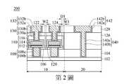
第2圖為本發明另一些實施例之電阻式隨機存取記憶體結構200的剖面示意圖。第2圖所示的電阻式隨機存取記憶體結構200與第1G圖所示的電阻式隨機存取記憶體結構100相似,差異在於第2圖的緩衝層124包括多個垂直部分。為了簡化說明,關於相同於第1G圖所繪示的元件及其形成製程步驟,在此不再詳述。FIG. 2 is a schematic cross-sectional view of a resistive random
請參照第2圖,緩衝層124包括一個第一垂直部分及多個第二垂直部分。當進行第1B圖所述的圖案化製程時,可在相鄰的該等記憶體單元110之間形成一溝槽。接著,形成緩衝層124並填入此溝槽中。如此一來,即可形成緩衝層124的第二垂直部分。緩衝層124的第一垂直部分位於間隙填充介電層122與第一低介電常數介電層126之間,且第一垂直部分定義陣列區10的邊緣。緩衝層124的各個第二垂直部分位於兩個相鄰的該等記憶體單元110之間且穿過間隙填充介電層122。在本實施例中,緩衝層124具有多個第二垂直部分,藉此可更加良好地支撐並保護位於陣列區10之中的元件。第一垂直部分具有第一寬度W1,第二垂直部分具有第二寬度W2。在一些實施例中,第一寬度W1相對於第二寬度W2的比例W1/W2為1-5。藉此,可有利於在同一步驟中同時形成第一垂直部分及第二垂直部分。Please refer to FIG. 2, the
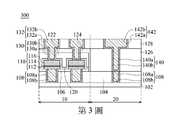
第3圖為本發明另一些實施例之電阻式隨機存取記憶體結構300的剖面示意圖。第3圖所示的電阻式隨機存取記憶體結構300與第1G圖所示的電阻式隨機存取記憶體結構100相似,差異在於第3圖的接觸插塞108也形成於周邊區20中。為了簡化說明,關於相同於第1G圖所繪示的元件及其形成製程步驟,在此不再詳述。FIG. 3 is a schematic cross-sectional view of a resistive random
請參照第3圖,周邊區20中的接觸插塞108位於第二導電插塞140下方且與第二導電插塞140直接接觸。當形成接觸插塞108於介電層104中時,可在周邊區20中預定形成第二導電插塞140的位置形成接觸插塞108。如此即可得到如第3圖所示的電阻式隨機存取記憶體結構300。在本實施例中,第二開口135的深度與第一開口125的深度的差異較前述實施例小。因此,在第一蝕刻製程期間,可使開口深度的控制較為容易。Referring to FIG. 3, the
第4圖為本發明另一些實施例之電阻式隨機存取記憶體結構400的剖面示意圖。第4圖所示的電阻式隨機存取記憶體結構400與第1G圖所示的電阻式隨機存取記憶體結構100相似,差異在於第4圖的第二導電線路142具有較大的厚度。為了簡化說明,關於相同於第1G圖所繪示的元件及其形成製程步驟,在此不再詳述。FIG. 4 is a schematic cross-sectional view of a resistive random
請參照第4圖,第二導電線路142的底表面低於第二低介電常數介電層128的底表面。可藉由控制第二蝕刻製程而得到如第4圖所示的電阻式隨機存取記憶體結構400。在一些實施例中,藉由增加第二蝕刻製程的蝕刻時間,以使第二溝槽137延伸進入至第一低介電常數介電層126中。在另一些實施例中,藉由增加第四蝕刻速率R4相對於該第三蝕刻速率R3的比例,以使第二溝槽137延伸至第一低介電常數介電層126中。在本實施例中,通過提高第二導電線路142的厚度,可提高邏輯電路的操作速度。Please refer to FIG. 4, the bottom surface of the second
緩衝層124的水平部分具有第一厚度T1,且第二導電線路142低於第一低介電常數介電層126的部分具有第三厚度T3。在一些實施例中,第三厚度T3相對於第一厚度T1的比例T3/T1為1-5。藉此,在第二蝕刻製程期間,可避免過度蝕刻對記憶體單元110或基板102(位於第二開口135下方的部分)造成傷害。The horizontal portion of the
綜上所述,在本發明實施例所提供之電阻式隨機存取記憶體結構中,形成一層緩衝層覆蓋整個陣列區,藉此可改善間隙填充介電層的機械強度。即使陣列區的間隙填充介電層與周邊區的介電層使用不同的介電材料,間隙填充介電層也不容易在化學機械研磨製程期間受到損傷。因此,可根據需求分別選擇陣列區與周邊區的介電材料。再者,在進行蝕刻製程時,緩衝層可保護位於陣列區的記憶體單元。因此,可在同一蝕刻製程中同時形成陣列區與周邊區的開口。如此一來,能夠明顯改善產品的良率及可靠度,而不會明顯增加製程的複雜度、生產成本及生產時間。In summary, in the resistive random access memory structure provided by the embodiment of the present invention, a buffer layer is formed to cover the entire array area, thereby improving the mechanical strength of the gap-filling dielectric layer. Even if different dielectric materials are used for the gap-fill dielectric layer of the array region and the dielectric layer of the peripheral region, the gap-fill dielectric layer is not easily damaged during the chemical mechanical polishing process. Therefore, the dielectric materials of the array area and the peripheral area can be selected according to requirements. Furthermore, during the etching process, the buffer layer can protect the memory cells located in the array area. Therefore, the openings of the array area and the peripheral area can be simultaneously formed in the same etching process. In this way, the yield and reliability of the product can be significantly improved without significantly increasing the complexity of the manufacturing process, production cost and production time.
雖然本發明已以數個較佳實施例揭露如上,然其並非用以限定本發明,任何所屬技術領域中具有通常知識者在不脫離本發明之精神和範圍內,當可作任意之更動與潤飾,因此本發明之保護範圍當視後附之申請專利範圍所界定者為準。Although the present invention has been disclosed in several preferred embodiments as described above, it is not intended to limit the present invention. Any person with ordinary knowledge in the technical field can make any changes without departing from the spirit and scope of the present invention. Retouching, therefore, the protection scope of the present invention shall be subject to the scope defined in the appended patent application.
100、200、300、400:電阻式隨機存取記憶體結構100, 200, 300, 400: resistive random access memory structure
10:陣列區10: Array area
130:第一導電插塞130: the first conductive plug
20:周邊區20: surrounding area
130a:導電襯層130a: conductive liner
102:基板102: substrate
130b:導電材料層130b: conductive material layer
104:介電層104: dielectric layer
132:第一導電線路132: The first conductive line
106:第一保護層106: The first protective layer
132a:導電襯層132a: conductive liner
108:接觸插塞108: contact plug
132b:導電材料層132b: conductive material layer
108a:襯層108a: lining
135:第二開口135: Second opening
108b:導電層108b: conductive layer
137:第二溝槽137: Second groove
110:記憶體單元110: memory unit
140:第二導電插塞140: second conductive plug
112:底電極層112: bottom electrode layer
140a:導電襯層140a: conductive liner
114:電阻轉態層114: resistance transition layer
140b:導電材料層140b: conductive material layer
116:頂電極層116: Top electrode layer
142:第二導電線路142: Second conductive line
120:第二保護層120: second protective layer
142a:導電襯層142a: conductive liner
122:間隙填充介電層122: gap-fill dielectric layer
142b:導電材料層142b: conductive material layer
124:緩衝層124: buffer layer
D1:距離D1: distance
125:第一開口125: first opening
W1:第一寬度W1: first width
126:第一低介電常數介電層126: the first low dielectric constant dielectric layer
W2:第二寬度W2: second width
127:第二溝槽127: Second groove
T1:第一厚度T1: first thickness
128:第二低介電常數介電層128: second low dielectric constant dielectric layer
T2:第二厚度T2: second thickness
第1A圖至第1G圖為本發明一些實施例之製造電阻式隨機存取記憶體結構的各步驟中所對應的剖面示意圖。 第2圖為本發明另一些實施例之電阻式隨機存取記憶體結構的剖面示意圖。 第3圖為本發明另一些實施例之電阻式隨機存取記憶體結構的剖面示意圖。 第4圖為本發明另一些實施例之電阻式隨機存取記憶體結構的剖面示意圖。FIGS. 1A to 1G are schematic cross-sectional views corresponding to the steps of manufacturing a resistive random access memory structure according to some embodiments of the present invention. FIG. 2 is a schematic cross-sectional view of a resistive random access memory structure according to other embodiments of the present invention. FIG. 3 is a schematic cross-sectional view of a resistive random access memory structure according to other embodiments of the invention. FIG. 4 is a schematic cross-sectional view of a resistive random access memory structure according to other embodiments of the invention.
10:陣列區10: Array area
20:周邊區20: surrounding area
100:電阻式隨機存取記憶體結構100: Resistive random access memory structure
102:基板102: substrate
104:介電層104: dielectric layer
106:第一保護層106: The first protective layer
108:接觸插塞108: contact plug
108a:襯層108a: lining
108b:導電層108b: conductive layer
110:記憶體單元110: memory unit
112:底電極層112: bottom electrode layer
114:電阻轉態層114: resistance transition layer
116:頂電極層116: Top electrode layer
120:第二保護層120: second protective layer
122:間隙填充介電層122: gap-fill dielectric layer
124:緩衝層124: buffer layer
126:第一低介電常數介電層126: the first low dielectric constant dielectric layer
128:第二低介電常數介電層128: second low dielectric constant dielectric layer
130:第一導電插塞130: the first conductive plug
130a:導電襯層130a: conductive liner
130b:導電材料層130b: conductive material layer
132:第一導電線路132: The first conductive line
132a:導電襯層132a: conductive liner
132b:導電材料層132b: conductive material layer
140:第二導電插塞140: second conductive plug
140a:導電襯層140a: conductive liner
140b:導電材料層140b: conductive material layer
142:第二導電線路142: Second conductive line
142a:導電襯層142a: conductive liner
142b:導電材料層142b: conductive material layer
D1:距離D1: distance
W1:第一寬度W1: first width
T1:第一厚度T1: first thickness
T2:第二厚度T2: second thickness
Claims (13)
Translated fromChinesePriority Applications (2)
| Application Number | Priority Date | Filing Date | Title |
|---|---|---|---|
| TW108111859ATWI692889B (en) | 2019-04-03 | 2019-04-03 | Resistive random access memory structure and manufacturing method thereof |
| US16/839,270US11329222B2 (en) | 2019-04-03 | 2020-04-03 | Resistive random access memory and manufacturing method thereof |
Applications Claiming Priority (1)
| Application Number | Priority Date | Filing Date | Title |
|---|---|---|---|
| TW108111859ATWI692889B (en) | 2019-04-03 | 2019-04-03 | Resistive random access memory structure and manufacturing method thereof |
Publications (2)
| Publication Number | Publication Date |
|---|---|
| TWI692889Btrue TWI692889B (en) | 2020-05-01 |
| TW202038490A TW202038490A (en) | 2020-10-16 |
Family
ID=71896066
Family Applications (1)
| Application Number | Title | Priority Date | Filing Date |
|---|---|---|---|
| TW108111859ATWI692889B (en) | 2019-04-03 | 2019-04-03 | Resistive random access memory structure and manufacturing method thereof |
Country Status (2)
| Country | Link |
|---|---|
| US (1) | US11329222B2 (en) |
| TW (1) | TWI692889B (en) |
Cited By (2)
| Publication number | Priority date | Publication date | Assignee | Title |
|---|---|---|---|---|
| CN114171464A (en)* | 2020-09-11 | 2022-03-11 | 长鑫存储技术有限公司 | Semiconductor structure and manufacturing method thereof |
| CN114171463A (en)* | 2020-09-11 | 2022-03-11 | 长鑫存储技术有限公司 | Semiconductor structure and manufacturing method thereof |
Families Citing this family (5)
| Publication number | Priority date | Publication date | Assignee | Title |
|---|---|---|---|---|
| TWI735031B (en)* | 2019-08-26 | 2021-08-01 | 華邦電子股份有限公司 | Resistive random access memory structure and manufacturing method thereof |
| US11737289B2 (en)* | 2020-12-09 | 2023-08-22 | International Business Machines Corporation | High density ReRAM integration with interconnect |
| CN116206969B (en)* | 2021-11-30 | 2025-09-26 | 长鑫存储技术有限公司 | Semiconductor structure manufacturing method and semiconductor structure |
| US12396369B2 (en) | 2021-11-30 | 2025-08-19 | Changxin Memory Technologies, Inc. | Method for fabricating semiconductor structure and semiconductor structure |
| CN115295576A (en)* | 2022-06-15 | 2022-11-04 | 昕原半导体(杭州)有限公司 | 1TnR resistive random access memory structure and preparation method thereof |
Citations (1)
| Publication number | Priority date | Publication date | Assignee | Title |
|---|---|---|---|---|
| TW201814837A (en)* | 2016-10-07 | 2018-04-16 | Targps科技公司 | Structure of resistive element and associated manufcturing method |
Family Cites Families (5)
| Publication number | Priority date | Publication date | Assignee | Title |
|---|---|---|---|---|
| US6946698B1 (en) | 2004-04-02 | 2005-09-20 | Taiwan Semiconductor Manufacturing Company, Ltd. | MRAM device having low-k inter-metal dielectric |
| WO2014142978A1 (en) | 2013-03-15 | 2014-09-18 | Intel Corporation | Logic chip including embedded magnetic tunnel junctions |
| US9548333B2 (en) | 2014-09-25 | 2017-01-17 | Qualcomm Incorporated | MRAM integration with low-K inter-metal dielectric for reduced parasitic capacitance |
| US9859335B1 (en) | 2016-12-02 | 2018-01-02 | United Microelectronics Corp. | Semiconductor device having memory cell structure |
| TWI735031B (en)* | 2019-08-26 | 2021-08-01 | 華邦電子股份有限公司 | Resistive random access memory structure and manufacturing method thereof |
- 2019
- 2019-04-03TWTW108111859Apatent/TWI692889B/enactive
- 2020
- 2020-04-03USUS16/839,270patent/US11329222B2/enactiveActive
Patent Citations (1)
| Publication number | Priority date | Publication date | Assignee | Title |
|---|---|---|---|---|
| TW201814837A (en)* | 2016-10-07 | 2018-04-16 | Targps科技公司 | Structure of resistive element and associated manufcturing method |
Cited By (3)
| Publication number | Priority date | Publication date | Assignee | Title |
|---|---|---|---|---|
| CN114171464A (en)* | 2020-09-11 | 2022-03-11 | 长鑫存储技术有限公司 | Semiconductor structure and manufacturing method thereof |
| CN114171463A (en)* | 2020-09-11 | 2022-03-11 | 长鑫存储技术有限公司 | Semiconductor structure and manufacturing method thereof |
| CN114171464B (en)* | 2020-09-11 | 2024-07-02 | 长鑫存储技术有限公司 | Semiconductor structure and manufacturing method thereof |
Also Published As
| Publication number | Publication date |
|---|---|
| US11329222B2 (en) | 2022-05-10 |
| US20200321521A1 (en) | 2020-10-08 |
| TW202038490A (en) | 2020-10-16 |
Similar Documents
| Publication | Publication Date | Title |
|---|---|---|
| TWI692889B (en) | Resistive random access memory structure and manufacturing method thereof | |
| US10957852B2 (en) | Resistance variable memory structure and method of forming the same | |
| CN106935544B (en) | Semiconductor device and method for forming the same | |
| KR102146761B1 (en) | Recap layer scheme to enhance rram performance | |
| CN102339869B (en) | There is semiconductor device and the manufacture method thereof of MIM capacitor | |
| TWI610343B (en) | Semiconductor structure having tapered damascene aperture and method of the same | |
| US8445991B2 (en) | Semiconductor device with MIM capacitor and method for manufacturing the same | |
| US9859335B1 (en) | Semiconductor device having memory cell structure | |
| US20140073128A1 (en) | Manufacturing method for metal line | |
| US12063875B2 (en) | Method for manufacturing resistive random access memory structure | |
| CN112838048A (en) | Interconnection structure and manufacturing method thereof | |
| CN111834392B (en) | Resistive random access memory structure and manufacturing method thereof | |
| JP4997682B2 (en) | Semiconductor device and manufacturing method thereof | |
| CN112531107B (en) | Resistive random access memory structure and manufacturing method thereof | |
| US12329046B2 (en) | Resistive memory structure comprising variable resistance and hard mask layers | |
| KR100661220B1 (en) | Metal wiring formation method using dual insulating film | |
| US11456207B2 (en) | Semiconductor device including metal interconnections having sidewall spacers thereon, and method for fabricating the same | |
| KR20080002027A (en) | Manufacturing method of semiconductor device | |
| US20090001581A1 (en) | Metal line of semiconductor device and method of forming the same | |
| KR100712817B1 (en) | Semiconductor Device and Forming Method | |
| CN115954324A (en) | Semiconductor structure and manufacturing method thereof | |
| CN114256289A (en) | Memristor and method of making the same | |
| JP2006324388A (en) | Semiconductor device and manufacturing method thereof | |
| KR20050035980A (en) | Method of forming metal wiring in flash memory device | |
| KR20090070442A (en) | Manufacturing Method of Semiconductor Device |