TWI692883B - Miniature components and their structures - Google Patents
Miniature components and their structuresDownload PDFInfo
- Publication number
- TWI692883B TWI692883BTW108114271ATW108114271ATWI692883BTW I692883 BTWI692883 BTW I692883BTW 108114271 ATW108114271 ATW 108114271ATW 108114271 ATW108114271 ATW 108114271ATW I692883 BTWI692883 BTW I692883B
- Authority
- TW
- Taiwan
- Prior art keywords
- light guide
- micro
- guide structure
- item
- patent application
- Prior art date
Links
- 239000000758substrateSubstances0.000claimsabstractdescription57
- 230000002093peripheral effectEffects0.000claimsabstractdescription25
- 239000004065semiconductorSubstances0.000claimsdescription54
- 238000005253claddingMethods0.000claimsdescription18
- 239000011248coating agentSubstances0.000claimsdescription2
- 238000000576coating methodMethods0.000claimsdescription2
- 239000010410layerSubstances0.000description117
- 238000000605extractionMethods0.000description6
- 239000011247coating layerSubstances0.000description5
- VYPSYNLAJGMNEJ-UHFFFAOYSA-NSilicium dioxideChemical compoundO=[Si]=OVYPSYNLAJGMNEJ-UHFFFAOYSA-N0.000description4
- 230000000694effectsEffects0.000description3
- 238000000034methodMethods0.000description3
- 229910052581Si3N4Inorganic materials0.000description2
- 239000000463materialSubstances0.000description2
- 235000012239silicon dioxideNutrition0.000description2
- 239000000377silicon dioxideSubstances0.000description2
- HQVNEWCFYHHQES-UHFFFAOYSA-Nsilicon nitrideChemical compoundN12[Si]34N5[Si]62N3[Si]51N64HQVNEWCFYHHQES-UHFFFAOYSA-N0.000description2
- 230000003139buffering effectEffects0.000description1
- 239000013078crystalSubstances0.000description1
- 230000007547defectEffects0.000description1
- 239000011521glassSubstances0.000description1
- 230000010354integrationEffects0.000description1
- 238000012986modificationMethods0.000description1
- 230000004048modificationEffects0.000description1
- 229910052594sapphireInorganic materials0.000description1
- 239000010980sapphireSubstances0.000description1
Images


Classifications
- H—ELECTRICITY
- H01—ELECTRIC ELEMENTS
- H01L—SEMICONDUCTOR DEVICES NOT COVERED BY CLASS H10
- H01L21/00—Processes or apparatus adapted for the manufacture or treatment of semiconductor or solid state devices or of parts thereof
- H01L21/67—Apparatus specially adapted for handling semiconductor or electric solid state devices during manufacture or treatment thereof; Apparatus specially adapted for handling wafers during manufacture or treatment of semiconductor or electric solid state devices or components ; Apparatus not specifically provided for elsewhere
- H01L21/683—Apparatus specially adapted for handling semiconductor or electric solid state devices during manufacture or treatment thereof; Apparatus specially adapted for handling wafers during manufacture or treatment of semiconductor or electric solid state devices or components ; Apparatus not specifically provided for elsewhere for supporting or gripping
- H01L21/6835—Apparatus specially adapted for handling semiconductor or electric solid state devices during manufacture or treatment thereof; Apparatus specially adapted for handling wafers during manufacture or treatment of semiconductor or electric solid state devices or components ; Apparatus not specifically provided for elsewhere for supporting or gripping using temporarily an auxiliary support
- H—ELECTRICITY
- H10—SEMICONDUCTOR DEVICES; ELECTRIC SOLID-STATE DEVICES NOT OTHERWISE PROVIDED FOR
- H10H—INORGANIC LIGHT-EMITTING SEMICONDUCTOR DEVICES HAVING POTENTIAL BARRIERS
- H10H20/00—Individual inorganic light-emitting semiconductor devices having potential barriers, e.g. light-emitting diodes [LED]
- H10H20/80—Constructional details
- H10H20/81—Bodies
- H10H20/819—Bodies characterised by their shape, e.g. curved or truncated substrates
- H10H20/82—Roughened surfaces, e.g. at the interface between epitaxial layers
- H—ELECTRICITY
- H01—ELECTRIC ELEMENTS
- H01L—SEMICONDUCTOR DEVICES NOT COVERED BY CLASS H10
- H01L2221/00—Processes or apparatus adapted for the manufacture or treatment of semiconductor or solid state devices or of parts thereof covered by H01L21/00
- H01L2221/67—Apparatus for handling semiconductor or electric solid state devices during manufacture or treatment thereof; Apparatus for handling wafers during manufacture or treatment of semiconductor or electric solid state devices or components; Apparatus not specifically provided for elsewhere
- H01L2221/683—Apparatus for handling semiconductor or electric solid state devices during manufacture or treatment thereof; Apparatus for handling wafers during manufacture or treatment of semiconductor or electric solid state devices or components; Apparatus not specifically provided for elsewhere for supporting or gripping
- H01L2221/68304—Apparatus for handling semiconductor or electric solid state devices during manufacture or treatment thereof; Apparatus for handling wafers during manufacture or treatment of semiconductor or electric solid state devices or components; Apparatus not specifically provided for elsewhere for supporting or gripping using temporarily an auxiliary support
- H01L2221/68318—Auxiliary support including means facilitating the separation of a device or wafer from the auxiliary support
- H—ELECTRICITY
- H01—ELECTRIC ELEMENTS
- H01L—SEMICONDUCTOR DEVICES NOT COVERED BY CLASS H10
- H01L2221/00—Processes or apparatus adapted for the manufacture or treatment of semiconductor or solid state devices or of parts thereof covered by H01L21/00
- H01L2221/67—Apparatus for handling semiconductor or electric solid state devices during manufacture or treatment thereof; Apparatus for handling wafers during manufacture or treatment of semiconductor or electric solid state devices or components; Apparatus not specifically provided for elsewhere
- H01L2221/683—Apparatus for handling semiconductor or electric solid state devices during manufacture or treatment thereof; Apparatus for handling wafers during manufacture or treatment of semiconductor or electric solid state devices or components; Apparatus not specifically provided for elsewhere for supporting or gripping
- H01L2221/68304—Apparatus for handling semiconductor or electric solid state devices during manufacture or treatment thereof; Apparatus for handling wafers during manufacture or treatment of semiconductor or electric solid state devices or components; Apparatus not specifically provided for elsewhere for supporting or gripping using temporarily an auxiliary support
- H01L2221/68363—Apparatus for handling semiconductor or electric solid state devices during manufacture or treatment thereof; Apparatus for handling wafers during manufacture or treatment of semiconductor or electric solid state devices or components; Apparatus not specifically provided for elsewhere for supporting or gripping using temporarily an auxiliary support used in a transfer process involving transfer directly from an origin substrate to a target substrate without use of an intermediate handle substrate
- H—ELECTRICITY
- H10—SEMICONDUCTOR DEVICES; ELECTRIC SOLID-STATE DEVICES NOT OTHERWISE PROVIDED FOR
- H10H—INORGANIC LIGHT-EMITTING SEMICONDUCTOR DEVICES HAVING POTENTIAL BARRIERS
- H10H20/00—Individual inorganic light-emitting semiconductor devices having potential barriers, e.g. light-emitting diodes [LED]
- H10H20/80—Constructional details
- H10H20/85—Packages
- H10H20/855—Optical field-shaping means, e.g. lenses
- H—ELECTRICITY
- H10—SEMICONDUCTOR DEVICES; ELECTRIC SOLID-STATE DEVICES NOT OTHERWISE PROVIDED FOR
- H10H—INORGANIC LIGHT-EMITTING SEMICONDUCTOR DEVICES HAVING POTENTIAL BARRIERS
- H10H20/00—Individual inorganic light-emitting semiconductor devices having potential barriers, e.g. light-emitting diodes [LED]
- H10H20/80—Constructional details
- H10H20/882—Scattering means
Landscapes
- Engineering & Computer Science (AREA)
- Physics & Mathematics (AREA)
- Condensed Matter Physics & Semiconductors (AREA)
- General Physics & Mathematics (AREA)
- Manufacturing & Machinery (AREA)
- Computer Hardware Design (AREA)
- Microelectronics & Electronic Packaging (AREA)
- Power Engineering (AREA)
- Led Devices (AREA)
Abstract
Description
Translated fromChinese本發明是有關於一種半導體結構,且特別是有關於一種微型元件及其結構。The present invention relates to a semiconductor structure, and particularly to a micro-element and its structure.
目前微型發光二極體的轉移主要是透過靜電力或磁力等方式,將暫時基板上的微型發光二極體轉板至接收基板上。一般來說,微型發光二極體會透過固定結構來固持而使微型發光二極體較容易自暫時基板上拾取,並運輸與轉移至接收基板上放置,且藉由固定結構來鞏固微型發光二極體於轉板時不會受到其他外在因素而影響品質。然而,由於固定結構與微型發光二極體周圍表面之接觸面的面積大小不易控制,因而使轉移後的微型發光二極體周圍表面仍殘留有固定結構,進而影響轉移後的微型發光二極體的出光。因此,如何在運輸與轉移微型發光二極體時避免固定結構殘留在微型發光二極體的周圍表面,已成為目前業界相當重視的課題之一。At present, the transfer of miniature light-emitting diodes mainly transfers the miniature light-emitting diodes on the temporary substrate to the receiving substrate by means of electrostatic force or magnetic force. Generally speaking, the miniature light-emitting diodes are held by a fixed structure so that the miniature light-emitting diodes can be easily picked up from the temporary substrate, transported and transferred to the receiving substrate, and the miniature light-emitting diodes are consolidated by the fixed structure The body will not be affected by other external factors when it is turned. However, since the area of the contact surface between the fixed structure and the surface around the miniature light-emitting diode is not easy to control, the fixed structure remains around the surface of the miniature light-emitting diode after the transfer, thereby affecting the miniature light-emitting diode after the transfer Light. Therefore, how to prevent the fixing structure from remaining on the surrounding surface of the miniature light-emitting diode when transporting and transferring the miniature light-emitting diode has become one of the topics that the industry attaches great importance to.
本發明提供一種微型元件結構,可使後續轉移時的斷點位於固定結構的犧牲部與外覆層的延伸部所定義出的預定斷裂區內,以避免固定結構的犧牲部殘留在轉移後的微型元件的周圍表面。The invention provides a micro-element structure, so that the breakpoint during the subsequent transfer can be located in a predetermined breaking area defined by the sacrificial portion of the fixed structure and the extension of the overcoat layer to avoid the sacrificial portion of the fixed structure remaining after the transfer The surrounding surface of the micro-element.
本發明提供一種微型元件,具有較佳的出光效果。The invention provides a micro-element with better light output effect.
本發明的微型元件結構包括基板、至少一微型元件以及至少一固定結構。微型元件配置於基板上。微型元件包括磊晶結構與外覆層。磊晶結構具有彼此相對的頂表面與底表面以及連接頂表面與底表面的周圍表面。外覆層包括接觸部與延伸部。接觸部覆蓋磊晶結構的周圍表面與底表面,而延伸部連接接觸部且往遠離周圍表面的水平方向延伸。固定結構配置於基板上。固定結構包括至少一連接部、至少一犧牲部以及至少一固定部。連接部配置於磊晶結構的頂表面與外覆層的延伸部上,犧牲部連接連接部與固定部。部分犧牲部接觸延伸部而定義出預定斷裂區,而固定部連接犧牲部且延伸至基板上。The micro-element structure of the present invention includes a substrate, at least one micro-element and at least one fixed structure. The micro element is arranged on the substrate. The micro device includes an epitaxial structure and an outer layer. The epitaxial structure has a top surface and a bottom surface opposed to each other and a peripheral surface connecting the top surface and the bottom surface. The outer coating layer includes a contact portion and an extension portion. The contact portion covers the surrounding surface and the bottom surface of the epitaxial structure, and the extension portion connects the contact portion and extends in a horizontal direction away from the surrounding surface. The fixing structure is arranged on the substrate. The fixing structure includes at least one connecting portion, at least one sacrificial portion, and at least one fixing portion. The connecting portion is disposed on the top surface of the epitaxial structure and the extension portion of the overcoat layer, and the sacrificial portion connects the connecting portion and the fixing portion. A portion of the sacrificial portion contacts the extended portion to define a predetermined breaking area, and the fixed portion connects the sacrificial portion and extends onto the substrate.
在本發明的一實施例中,上述的固定結構的犧牲部與外覆層的延伸部之間具有夾角,而夾角介於80度至120度之間。In an embodiment of the present invention, the sacrificial portion of the above-mentioned fixing structure has an angle between the extending portion of the outer cover and the angle is between 80 degrees and 120 degrees.
在本發明的一實施例中,上述的固定結構的犧牲部垂直於外覆層的延伸部。In an embodiment of the invention, the sacrificial portion of the above-mentioned fixing structure is perpendicular to the extending portion of the outer cover.
在本發明的一實施例中,上述的固定結構的犧牲部的延伸方向垂直於基板。In an embodiment of the present invention, the extending direction of the sacrificial portion of the fixing structure is perpendicular to the substrate.
在本發明的一實施例中,上述的微型元件結構更包括至少一導光結構,配置於微型元件上。導光結構位於固定結構的連接部與磊晶結構的頂表面之間,以及位於固定結構的連接部與外覆層的延伸部之間。In an embodiment of the invention, the above-mentioned micro device structure further includes at least one light guide structure, which is disposed on the micro device. The light guide structure is located between the connection portion of the fixed structure and the top surface of the epitaxial structure, and between the connection portion of the fixed structure and the extension portion of the outer cladding layer.
在本發明的一實施例中,上述的外覆層於基板上的正投影面積與導光結構於基板上的正投影面積的比值大於等於0.8且小於等於1。In an embodiment of the invention, the ratio of the orthographic projection area of the overcoat layer on the substrate to the orthographic projection area of the light guide structure on the substrate is greater than or equal to 0.8 and less than or equal to 1.
在本發明的一實施例中,上述的固定結構的第一厚度大於導光結構的第二厚度。In an embodiment of the invention, the first thickness of the above-mentioned fixed structure is greater than the second thickness of the light guide structure.
在本發明的一實施例中,上述的磊晶結構包括第一型半導體層、發光層與第二型半導體層。發光層位於第一型半導體層與第二型半導體層之間。第一型半導體層具有頂表面。導光結構的面積大於頂表面的面積,且頂表面的面積與導光結構的面積的比值大於等於0.5且小於等於0.95。In an embodiment of the invention, the above epitaxial structure includes a first type semiconductor layer, a light emitting layer and a second type semiconductor layer. The light emitting layer is located between the first type semiconductor layer and the second type semiconductor layer. The first type semiconductor layer has a top surface. The area of the light guide structure is greater than the area of the top surface, and the ratio of the area of the top surface to the area of the light guide structure is greater than or equal to 0.5 and less than or equal to 0.95.
在本發明的一實施例中,上述的導光結構與第一型半導體層的第一接觸表面的粗糙度大於導光結構與固定結構的第二接觸表面的粗糙度。In an embodiment of the invention, the roughness of the first contact surface between the light guide structure and the first type semiconductor layer is greater than the roughness of the second contact surface of the light guide structure and the fixed structure.
在本發明的一實施例中,上述的導光結構與第一型半導體層的第一接觸表面的粗糙度大於導光結構與外覆層的延伸部的第二接觸表面的粗糙度。In an embodiment of the invention, the roughness of the first contact surface between the light guide structure and the first type semiconductor layer is greater than the roughness of the second contact surface of the extension portion of the light guide structure and the overcoat layer.
在本發明的一實施例中,上述的外覆層與磊晶結構的周圍表面之間具有最小水平距離,且最小水平距離大於等於1微米。In an embodiment of the invention, there is a minimum horizontal distance between the overcoat layer and the surrounding surface of the epitaxial structure, and the minimum horizontal distance is greater than or equal to 1 micrometer.
在本發明的一實施例中,上述的外覆層的延伸部的表面切齊磊晶結構的頂表面。In an embodiment of the present invention, the surface of the extension portion of the overcoat layer cuts the top surface of the epitaxial structure.
在本發明的一實施例中,上述的磊晶結構於基板上的正投影面積與外覆層於基板上的正投影面積的比值大於等於0.5且小於等於0.95。In an embodiment of the invention, the ratio of the orthographic projection area of the epitaxial structure on the substrate to the orthographic projection area of the overcoat layer on the substrate is greater than or equal to 0.5 and less than or equal to 0.95.
本發明的微型元件包括磊晶結構、外覆層以及第一導光結構。磊晶結構具有彼此相對的頂表面與底表面以及連接頂表面與底表面的周圍表面。外覆層包括接觸部與延伸部。接觸部覆蓋磊晶結構的周圍表面與底表面,而延伸部連接接觸部且往遠離周圍表面的水平方向延伸。第一導光結構配置於磊晶結構的頂表面與外覆層的延伸部上。第一導光結構於水平面上的正投影面積大於等於外覆層於水平面上的正投影面積。The micro device of the present invention includes an epitaxial structure, an overcoat layer and a first light guide structure. The epitaxial structure has a top surface and a bottom surface opposed to each other and a peripheral surface connecting the top surface and the bottom surface. The outer coating layer includes a contact portion and an extension portion. The contact portion covers the surrounding surface and the bottom surface of the epitaxial structure, and the extension portion connects the contact portion and extends in a horizontal direction away from the surrounding surface. The first light guide structure is disposed on the top surface of the epitaxial structure and the extension of the outer cladding layer. The orthographic projection area of the first light guide structure on the horizontal plane is greater than or equal to the orthographic projection area of the outer coating layer on the horizontal plane.
在本發明的一實施例中,上述的微型元件更包括第二導光結構。第二導光結構配置於第一導光結構上,而第一導光結構位於磊晶結構與第二導光結構之間。第一導光結構的第一表面積大於第二導光結構的第二表面積。In an embodiment of the invention, the aforementioned micro-device further includes a second light guide structure. The second light guide structure is disposed on the first light guide structure, and the first light guide structure is located between the epitaxial structure and the second light guide structure. The first surface area of the first light guide structure is greater than the second surface area of the second light guide structure.
在本發明的一實施例中,上述的第一導光結構具有第一厚度,而第二導光結構具有第二厚度,且第二厚度大於第一厚度。In an embodiment of the invention, the first light guide structure has a first thickness, and the second light guide structure has a second thickness, and the second thickness is greater than the first thickness.
在本發明的一實施例中,上述的磊晶結構包括第一型半導體層、發光層以及第二型半導體層。發光層位於第一型半導體層與第二型半導體層之間。第一型半導體層具有頂表面。第一導光結構的面積大於頂表面的面積,且頂表面的面積與第一導光結構的面積的比值大於等於0.5且小於等於0.95。In an embodiment of the invention, the above epitaxial structure includes a first type semiconductor layer, a light emitting layer, and a second type semiconductor layer. The light emitting layer is located between the first type semiconductor layer and the second type semiconductor layer. The first type semiconductor layer has a top surface. The area of the first light guide structure is greater than the area of the top surface, and the ratio of the area of the top surface to the area of the first light guide structure is greater than or equal to 0.5 and less than or equal to 0.95.
在本發明的一實施例中,上述的第一導光結構與第一型半導體層的第一接觸表面的粗糙度大於第一導光結構與第二導光結構的第二接觸表面的粗糙度。In an embodiment of the invention, the roughness of the first contact surface between the first light guide structure and the first type semiconductor layer is greater than the roughness of the second contact surface of the first light guide structure and the second light guide structure .
在本發明的一實施例中,上述的第一導光結構與第一型半導體層的第一接觸表面的粗糙度大於第一導光結構與外覆層的延伸部的第三接觸表面的粗糙度。In an embodiment of the present invention, the roughness of the first contact surface between the first light guide structure and the first type semiconductor layer is greater than the roughness of the third contact surface of the extension portion of the first light guide structure and the overcoat layer degree.
在本發明的一實施例中,上述的外覆層與磊晶結構的周圍表面之間具有最小水平距離,且最小水平距離大於等於1微米。In an embodiment of the invention, there is a minimum horizontal distance between the overcoat layer and the surrounding surface of the epitaxial structure, and the minimum horizontal distance is greater than or equal to 1 micrometer.
在本發明的一實施例中,上述的外覆層於水平面上的正投影面積與第一導光結構於水平面上的正投影面積的比值大於等於0.8且小於等於1。In an embodiment of the present invention, the ratio of the orthographic projection area of the outer cover layer on the horizontal plane to the orthographic projection area of the first light guide structure on the horizontal plane is greater than or equal to 0.8 and less than or equal to 1.
在本發明的一實施例中,上述的磊晶結構於水平面上的正投影面積與外覆層於水平面上的正投影面積的比值大於等於0.5且小於等於0.95。In an embodiment of the invention, the ratio of the orthographic projection area of the epitaxial structure on the horizontal plane to the orthographic projection area of the overcoat layer on the horizontal plane is greater than or equal to 0.5 and less than or equal to 0.95.
基於上述,在本發明的微型元件結構中,微型元件結構的外覆層具有接觸固定結構的犧牲部的延伸部,其中延伸部往遠離微型元件的周圍表面的水平方向延伸,且部分犧牲部接觸與延伸部定義出預定斷裂區。因此,在後續轉移微型元件結構時,固定結構的斷點會位於預定斷裂區內,可以避免固定結構的犧牲部殘留在轉移後的微型元件的周圍表面。藉此,可提高本發明的微型元件的發光效率。Based on the above, in the micro-element structure of the present invention, the outer layer of the micro-element structure has an extension portion that contacts the sacrificial portion of the fixed structure, wherein the extension portion extends in a horizontal direction away from the peripheral surface of the micro-element, and part of the sacrificial portion contacts The predetermined fracture zone is defined with the extension. Therefore, in the subsequent transfer of the micro-element structure, the break point of the fixed structure will be located in the predetermined breaking area, which can avoid the sacrificial portion of the fixed structure remaining on the surrounding surface of the transferred micro-element. Thereby, the luminous efficiency of the micro-device of the present invention can be improved.
為讓本發明的上述特徵和優點能更明顯易懂,下文特舉實施例,並配合所附圖式作詳細說明如下。In order to make the above-mentioned features and advantages of the present invention more obvious and understandable, the embodiments are specifically described below in conjunction with the accompanying drawings for detailed description as follows.
本發明的實施例描述微型元件(例如微型發光二極體(Micro LED))的結構,使之準備好拾取及轉移到接收基板。接收基板可例如為顯示基板、發光基板、具諸如電晶體或積體電路(ICs)等功能元件的基板或具其他具線路的基板,但不以此為限。雖然本發明的一些實施例特定於描述包含p-n二極體的微型發光二極體,但應理解本發明的實施例不限於此,某些實施例亦可應用到其他微型元件,該等微型元件依此一方式設計成控制執行預定電子功能(例如二極體、電晶體、積體電路)或光子功能(LED、雷射)。Embodiments of the present invention describe the structure of micro-elements (such as Micro LEDs), making them ready to be picked up and transferred to the receiving substrate. The receiving substrate may be, for example, a display substrate, a light-emitting substrate, a substrate with functional elements such as transistors or integrated circuits (ICs), or another substrate with wiring, but not limited thereto. Although some embodiments of the present invention are specific to describing miniature light emitting diodes including pn diodes, it should be understood that embodiments of the present invention are not limited to this, and some embodiments can also be applied to other miniature devices, such miniature devices In this way, it is designed to control the execution of predetermined electronic functions (such as diodes, transistors, integrated circuits) or photonic functions (LED, laser).
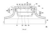
圖1A繪示為本發明一實施例的一種微型元件結構的剖面示意圖。請參照圖1A,本實施例的微型元件結構100包括基板110、至少一微型元件120(圖1 A中示意地繪示一個)以及至少一固定結構130(圖1 A中示意地繪示一個)。微型元件120配置於基板110上。微型元件120包括磊晶結構121與外覆層122,其中磊晶結構121具有彼此相對的頂表面121a與底表面121b以及連接頂表面121a與底表面121b的周圍表面121c。外覆層122包括接觸部122a與延伸部122b。接觸部122a覆蓋磊晶結構121的周圍表面121c與底表面121b,而延伸部122b連接接觸部122a且往遠離周圍表面121c的水平方向H延伸。固定結構130配置於基板110上。固定結構130包括至少一連接部131(圖1 A中示意地繪示一個)、至少一犧牲部132(圖1 A中示意地繪示一個)以及至少一固定部133(圖1 A中示意地繪示一個)。連接部131配置於磊晶結構121的頂表面121a與外覆層122上,而犧牲部132連接連接部131與固定部133。特別是,部分犧牲部132接觸延伸部122b而定義出預定斷裂區R。固定部133連接犧牲部132且延伸至基板110上。此處,固定部133可以直接觸基板110而具更佳的抓地力,或是透過一緩衝層(未繪示)連接基板110而具更佳的緩衝功能。FIG. 1A is a schematic cross-sectional view of a micro device structure according to an embodiment of the invention. 1A, the
進一步來說,本實施例的基板110例如是一塑膠基板、一玻璃基板或一藍寶石基板等的暫時基板,但不以此為限。微型元件120例如是一微型發光二極體,其中微型元件120的一最大尺寸小於等於100微米,厚度小於等於15微米,後續可以轉移整合及組裝到異質整合系統,包括微型顯示器至大面積顯示器等任何尺寸的基板,但不以此為限。在本實施例中,微型元件120的磊晶結構121包括第一型半導體層1211、發光層1212以及第二型半導體層1213。發光層1212位於第一型半導體層1211與第二型半導體層1213之間,且第一型半導體層1211位於固定結構130的連接部131與發光層1212之間。第一型半導體層1211具有頂表面121a,而第二型半導體層1213具有底表面121b。再者,本實施例的微型元件120更包括第一型電極123與第二型電極124。第一型電極123與第二型電極124位於磊晶結構121的底表面121b上,且固定結構130相對遠離第一型電極123與第二型電極124,避免固定結構130影響第一型電極123與第二型電極124。換言之,本實施例的微型元件120具體化為覆晶式微型元件,但並不以此為限。Further, the
再者,本實施例的外覆層122的接觸部122a覆蓋磊晶結構121的周圍表面121c與底表面121b。此處,外覆層122可具有反射的功能,可反射磊晶結構121的發光層1212所發出的光,以提高出光效率。在一實施例中,外覆層122可例如是分散式布拉格反射鏡(Distributed Bragg Reflector,DBR),但不以此為限。外覆層122亦可具有保護絕緣的功能,在一實施例中,外覆層122的材料可例如是二氧化矽或氮化矽,但不以此為限。如圖1 A所示,本實施例的外覆層122的延伸部122b連接接觸部122a且往遠離磊晶結構121的周圍表面121c的水平方向H延伸。藉由外覆層122的延伸部122b的設計來隔開固定結構130與磊晶結構121,而使固定結構130的犧牲部132及固定部133不接觸微型元件120的磊晶結構121。Furthermore, the
更具體來說,請繼續參照圖1 A,在本實施例中,固定結構130的犧牲部132與外覆層122的延伸部122b之間具有夾角A,較佳地,夾角A例如是介於80度至120度之間。當夾角A小於80度時,固定結構130的犧牲部132會過度接近接觸外覆層122的接觸部122a而造成後續轉移的困難度。當夾角A大於120度時,固定結構130的犧牲部132會過度遠離外覆層122的接觸部122a而可能使支撐力不夠。在一實施例中,固定結構130的犧牲部132亦可垂直於外覆層122的延伸部122b。在另一實施例中,固定結構130的犧牲部132的延伸方向也可垂直於基板110,可使固定結構130於基板110上較緊密排列,以增加微型元件120的排列密度。此處,外覆層122的延伸部122b連接固定結構130的犧牲部132的一端至磊晶結構121的周圍表面121c之間具有一最小水平距離D1。較佳地,最小水平距離D1例如是大於等於1微米,可使固定結構130的犧牲部132不會太過接近磊晶結構121,避免後續轉移後的殘留。此外,外覆層122的延伸部122b的表面122c切齊磊晶結構121的頂表面121a。也就是說,外覆層122的延伸部122b的延伸方向H與磊晶結構121的頂表面121a的延伸方向平行且相同。More specifically, please continue to refer to FIG. 1A. In this embodiment, an angle A is formed between the
請再參考圖1 A,本實施例的磊晶結構121於基板110上的正投影完全重疊於外覆層122於基板110上的正投影。磊晶結構121於基板110上的正投影面積小於外覆層122於基板110上的正投影面積。較佳地,磊晶結構121於基板110上的正投影面積與外覆層122於基板110上的正投影面積的比值大於等於0.5且小於等於0.95。透過外覆層122的正投影面積大於磊晶結構121的正投影面積,來使固定結構130的犧牲部132與固定部133不接觸微型元件120的磊晶結構121。Referring again to FIG. 1A, the orthographic projection of the
為了更進一步提高發光效率,本實施例的微型元件結構100更包括至少一導光結構140(圖1 A中示意地繪示一個),其中導光結構140配置於微型元件120上,且覆蓋磊晶結構121的頂表面121a以及外覆層122的延伸部122b。更具體來說,導光結構140位於固定結構130的連接部131與磊晶結構121的頂表面121a之間,以及位於固定結構130的連接部131與外覆層122的延伸部122b之間。此處,如圖1A所示,導光結構140直接接觸固定結構130的連接部131、磊晶結構121的頂表面121a及外覆層122的延伸部122b。特別是,固定結構130的厚度H1大於導光結構140的厚度H2,可具有較佳的固定力。外覆層122於基板110上的正投影面積與導光結構140於基板110上的正投影面積的比值例如是大於等於0.8且小於等於1。換言之,透過外覆層122的延伸部122b的設計,使得一般因微型元件過小而無法在微型元件的磊晶結構的頂表面上配置整面的導光結構140,本發明的導光結構140於基板110上的正投影面積大於磊晶結構121於基板110上的正投影面積,可具有較佳的導光效果。較佳地,磊晶結構121的頂表面121a的面積與導光結構140的面積的比值例如是大於等於0.5且小於等於0.95。當比值小於0.5時,導光結構140佔據的空間太大而影響後續轉移良率。當比值大於0.95時,則會讓導光結構140配置於磊晶結構121的頂表面121a的製程裕度過小而易偏移,無法全面配置。In order to further improve the luminous efficiency, the
簡言之,在本實施例的微型元件結構100中,固定結構130僅有部分犧牲部132與微型元件120的外覆層122的延伸部122b接觸。也就是說,固定結構130不接觸微型元件120的磊晶結構121。因此,當微型元件結構100中的微型元件120從基板110上拾取並運輸與轉移時,拾取微型元件120的力會使固定結構130從犧牲部132與延伸部122b定義出的預定斷裂區R發生斷裂,而使微型元件120與固定結構130的犧牲部132及固定部133分離。藉此,可避免固定結構130的犧牲部132殘留在微型元件120的周圍表面121c上而影響出光並造成轉移時的缺陷。此外,留在拾取、轉移後的微型元件120上的固定結構130的連接部131可視為是一種導光結構,可提高微型元件120的出光效率。In short, in the
圖1B繪示為本發明一實施例的另一種微型元件的剖面示意圖。請同時參照圖1A與圖1B,本實施例的導光結構140’與第一型半導體層1211的接觸表面141的粗糙度大於導光結構140’與固定結構130的接觸表面142的粗糙度。導光結構140’與第一型半導體層1211的接觸表面141的粗糙度也大於導光結構140’與外圍層122的延伸部122b的接觸表面143的粗糙度。此處,所指的粗糙度是中心線平均粗糙度(Ra ,arithmetical mean deviation)。也就是說,導光結構140’在面向微型元件120一側的中央區域(即第一型半導體層1211所在之處)的粗糙度大於環繞中央區域的周圍區域(即外覆層122的延伸部122b所在之處)的粗糙度,可以更進一步提高出光效率,特別是中央區域的出光率以增加正向光。FIG. 1B is a schematic cross-sectional view of another micro device according to an embodiment of the invention. 1A and 1B, the roughness of the
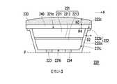
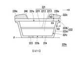
圖2A繪示為本發明一實施例的一種微型元件的剖面示意圖。圖2B繪示為圖2A的微型元件的俯視示意圖,其中圖2B的微型元件是沿圖2A的線Ⅰ-Ⅰ’所繪示。請同時參照圖2A與圖2B,本實施例的微型元件220包括磊晶結構221、外覆層222、第一導光結構240以及第二導光結構230。磊晶結構221具有彼此相對的頂表面221a與底表面221b以及連接頂表面221a與底表面221b的周圍表面221c。外覆層222包括接觸部222a與延伸部222b。接觸部222a覆蓋磊晶結構221的周圍表面221c與底表面221b,而延伸部222b連接接觸部222a且往遠離周圍表面221c的水平方向H延伸。第一導光結構240配置於磊晶結構221的頂表面221a與外覆層222的延伸部222b上。第二導光結構230配置於第一導光結構240上,而第一導光結構240位於磊晶結構221與第二導光結構230之間。較佳地,第一導光結構240的表面積大於第二導光結構230的表面積,且第一導光結構240於水平面P上的正投影面積大於外覆層222於水平面P上的正投影面積。2A is a schematic cross-sectional view of a micro device according to an embodiment of the invention. FIG. 2B is a schematic top view of the micro-device of FIG. 2A, wherein the micro-device of FIG. 2B is drawn along line I-I' of FIG. 2A. 2A and 2B at the same time, the
具體來說,在本實施例中,磊晶結構221包括第一型半導體層2211、發光層2212以及第二型半導體層2213。發光層2212位於第一型半導體層2211與第二型半導體層2213之間,且第一型半導體層2211位於第一導光結構240與發光層2212之間。第一型半導體層2211具有頂表面221a,而第二型半導體層2213具有底表面221b。再者,本實施例的微型元件220更包括第一型電極223與第二型電極224。第一型電極223與第二型電極224位於磊晶結構221的底表面221b上,且第一導光結構240與第二導光結構230相對遠離第一型電極223與第二型電極224,避免影響第一型電極223與第二型電極224。換言之,本實施例的微型元件220具體化為覆晶式微型元件,但並不以此為限。Specifically, in this embodiment, the
再者,本實施例的外覆層222的接觸部222a覆蓋磊晶結構221的周圍表面221c與底表面221b。此處,外覆層222可具有反射的功能,可反射磊晶結構221的發光層2212所發出的光,以提高出光效率。於一實施例中,外覆層222可例如是分散式布拉格反射鏡(Distributed Bragg Reflector,DBR),但不以此為限。外覆層222亦可具有保護絕緣的功能,於另一實施例中,外覆層222的材料可例如是二氧化矽或氮化矽,但不以此為限。外覆層222的延伸部222b連接接觸部222a且往遠離磊晶結構221的周圍表面221c的水平方向H延伸。此處,外覆層222的延伸部222b相對遠離磊晶結構221的周圍表面221c的一端至周圍表面221c之間具有一最小水平距離D2,較佳地,最小水平距離D2例如是大於等於1微米。此外,外覆層222的延伸部222b的表面222c切齊磊晶結構221的頂表面221a,也就是說,外覆層222的延伸部222b的延伸方向H與磊晶結構221的頂表面221a的延伸方向平行且相同。Furthermore, the
請再同時參照圖2A與圖2B,本實施例的磊晶結構221於水平面P上的正投影完全重疊於外覆層222於水平面P上的正投影內。也就是說,磊晶結構221於水平面P上的正投影面積小於外覆層222於水平面P上的正投影面積。較佳地,磊晶結構221於水平面P上的正投影面積與外覆層222於水平面P上的正投影面積的比值大於等於0.5且小於等於0.95。再者,外覆層222於水平面P上的正投影面積小於等於第一導光結構240於水平面P上的正投影面積。較佳地,外覆層222於水平面P上的正投影面積與第一導光結構240於水平面P上的正投影面積的比值例如是大於等於0.8且小於等於1。2A and 2B at the same time, the orthographic projection of the
更具體來說,本實施例的第一導光結構240的面積大於頂表面221a的面積,且頂表面221a的面積與第一導光結構240的面積的比值例如是大於等於0.5且小於等於0.95。當比值小於0.5時,會使第一導光結構240佔據的空間太大而影響後續轉移的良率。當比值大於0.95時,則會讓第一導光結構240配置於頂表面221a的製程裕度過小而易偏移,無法全面配置。換言之,透過外覆層222的延伸部222b的設計,相較於一般因微型元件過小而無法在微型元件上配置整面的導光結構,本發明的第一導光結構240於水平面P上的正投影面積大於磊晶結構221於水平面P上的正投影面積,可具有較佳的導光效果。再者,本實施例的第二導光結構230的厚度H3大於第一導光結構240的厚度H4,透過厚度不同可以增加出光。第二導光結構230的面積小於頂表面221a的面積,其中第二導光結構230的面積與頂表面221a的面積的比值例如是大於等於0.5且小於等於0.95。再者,第二導光結構230配置於頂表面221a的中央區域,透過此種設計可以增加中央區域的正向出光。More specifically, the area of the first
此外,為了提高導光效率,如圖2C所示,本實施例的第一導光結構240’與第一型半導體層2211的接觸表面241的粗糙度大於第一導光結構240’與第二導光結構230的接觸表面242的粗糙度。第一導光結構240’與第一型半導體層2211的接觸表面241的粗糙度也大於第一導光結構240’與外覆層222的延伸部222b的接觸表面243的粗糙度。此處,所指的粗糙度是中心線平均粗糙度(Ra ,arithmetical mean deviation)。也就是說,第一導光結構240’在面向磊晶結構221一側的中央區域(即第一型半導體層2211所在之處)的粗糙度大於環繞中央區域的周圍區域(即外覆層222的延伸部222b所在之處)的粗糙度,可以更進一步提高出光效率,特別是中央區域的出光率以增加正向光。In addition, in order to improve the light guide efficiency, as shown in FIG. 2C, the roughness of the
需要說明的是,在本實施例的微型元件220中,第二導光結構230的配置位置與圖1 A中的微型元件結構100的固定結構130的連接部131相似。在對圖1A的微型元件結構100中的微型元件120進行轉移時,固定結構130的斷點會落在預定斷裂區R,而留在拾取、轉移後的微型元件120上的固定結構130的連接部131可視為是圖2A的微型元件220中的第二導光結構230,可用來提升微型元件220的出光效率。It should be noted that, in the
在此必須說明的是,下述實施例沿用前述實施例的元件標號與部分內容,其中採用相同的標號來表示相同或近似的元件,並且省略了相同技術內容的說明。關於省略部分的說明可參照前述實施例,下述實施例不再重複贅述。It must be noted here that the following embodiments follow the element numbers and partial contents of the foregoing embodiments, wherein the same reference numbers are used to indicate the same or similar elements, and the description of the same technical content is omitted. For the description of the omitted parts, reference may be made to the foregoing embodiments, and the following embodiments will not be repeated.
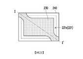
圖3A繪示為本發明另一實施例的一種微型元件的剖面示意圖。圖3B繪示為圖3A的微型元件的俯視示意圖,其中圖3B的微型元件是沿圖3A的線Ⅱ-Ⅱ’所繪示。請同時參照圖2A、圖2B、圖3A及圖3B,本實施例的微型元件220a與圖2A的微型元件220相似,兩者的差異在於:本實施例的第二導光結構230a僅配置於第一導光結構240’上的其中一對角的角落。也就是說,第二導光結構230a主要是設置在周圍區域(即外覆層222的延伸部222b所在之處)及局部中央區域(即第一型半導體層2211所在之處)中。藉此控制後續拾取的製程良率。3A is a schematic cross-sectional view of a micro device according to another embodiment of the invention. 3B is a schematic top view of the micro-device of FIG. 3A, wherein the micro-device of FIG. 3B is drawn along the line II-II' of FIG. 3A. Please refer to FIG. 2A, FIG. 2B, FIG. 3A and FIG. 3B at the same time. The micro-device 220a of this embodiment is similar to the
綜上所述,在本發明的微型元件結構中,微型元件結構的外覆層具有接觸固定結構的犧牲部的延伸部,其中延伸部往遠離微型元件的周圍表面的水平方向延伸,且部分犧牲部接觸與延伸部定義出預定斷裂區。因此,在後續轉移微型元件結構時,固定結構的斷點會位於預定斷裂區內,可以避免固定結構的犧牲部殘留在轉移後的微型元件的周圍表面。藉此,可提高本發明的微型元件的發光效率。In summary, in the micro-element structure of the present invention, the outer layer of the micro-element structure has an extension portion that contacts the sacrificial portion of the fixed structure, wherein the extension portion extends horizontally away from the surrounding surface of the micro-element and is partially sacrificed The partial contact and extension define a predetermined fracture zone. Therefore, in the subsequent transfer of the micro-element structure, the break point of the fixed structure will be located in the predetermined breaking area, which can avoid the sacrificial portion of the fixed structure remaining on the surrounding surface of the transferred micro-element. Thereby, the luminous efficiency of the micro-device of the present invention can be improved.
雖然本發明已以實施例揭露如上,然其並非用以限定本發明,任何所屬技術領域中具有通常知識者,在不脫離本發明的精神和範圍內,當可作些許的更動與潤飾,故本發明的保護範圍當視後附的申請專利範圍所界定者為準。Although the present invention has been disclosed as above with examples, it is not intended to limit the present invention. Any person with ordinary knowledge in the technical field can make some changes and modifications without departing from the spirit and scope of the present invention. The scope of protection of the present invention shall be subject to the scope defined in the appended patent application.
100:微型元件結構110:基板120、220:微型元件121、221:磊晶結構121a、221a:頂表面121b、221b:底表面121c、221c:周圍表面1211、2211:第一型半導體層1212、2212:發光層1213、2213:第二型半導體層122、222:外覆層122a、222a:接觸部122b、222b:延伸部122c、222c:表面123、223:第一型電極124、224:第二型電極130:固定結構131:連接部132:犧牲部133:固定部140、140’:導光結構141、142、143、241、242、243:接觸表面230、230a:第二導光結構240、240’:第一導光結構A:夾角D1、D2:最小水平距離H:水平方向H1、H2、H3、H4:厚度P:水平面R:預定斷裂區100: micro-component structure110:
圖1A繪示為本發明一實施例的一種微型元件結構的剖面示意圖。 圖1B繪示為本發明另一實施例的一種微型元件結構的剖面示意圖。 圖2A繪示為本發明一實施例的一種微型元件的剖面示意圖。 圖2B繪示為圖2A的微型元件的俯視示意圖。 圖2C繪示為本發明另一實施例的一種微型元件的剖面示意圖。 圖3A繪示為本發明另一實施例的一種微型元件的剖面示意圖。 圖3B繪示為圖3A的微型元件的俯視示意圖。FIG. 1A is a schematic cross-sectional view of a micro device structure according to an embodiment of the invention. FIG. 1B is a schematic cross-sectional view of a micro-device structure according to another embodiment of the invention. 2A is a schematic cross-sectional view of a micro device according to an embodiment of the invention. FIG. 2B is a schematic top view of the micro-device of FIG. 2A. 2C is a schematic cross-sectional view of a micro device according to another embodiment of the invention. 3A is a schematic cross-sectional view of a micro device according to another embodiment of the invention. FIG. 3B is a schematic top view of the micro-device of FIG. 3A.
100:微型元件結構100: micro-component structure
110:基板110: substrate
120:微型元件120: Miniature components
121:磊晶結構121: Epitaxial structure
121a:頂表面121a: top surface
121b:底表面121b: bottom surface
121c:周圍表面121c: surrounding surface
1211:第一型半導體層1211: Type 1 semiconductor layer
1212:發光層1212: Luminous layer
1213:第二型半導體層1213: Type 2 semiconductor layer
122:外覆層122: outer cover
122a:接觸部122a: contact
122b:延伸部122b: Extension
122c:表面122c: surface
123:第一型電極123: Type 1 electrode
124:第二型電極124: Type 2 electrode
130:固定結構130: fixed structure
131:連接部131: Connection
132:犧牲部132: Sacrifice
133:固定部133: Fixed part
140:導光結構140: light guide structure
A:夾角A: Angle
D1:水平距離D1: horizontal distance
H:水平方向H: horizontal direction
H1、H2:厚度H1, H2: thickness
R:預定斷裂區R: predetermined break zone
Claims (23)
Translated fromChinesePriority Applications (3)
| Application Number | Priority Date | Filing Date | Title |
|---|---|---|---|
| TW108114271ATWI692883B (en) | 2019-04-24 | 2019-04-24 | Miniature components and their structures |
| US16/522,686US11171271B2 (en) | 2019-04-24 | 2019-07-26 | Micro device and structure thereof |
| US17/489,789US12439747B2 (en) | 2019-04-24 | 2021-09-30 | Micro device and display apparatus |
Applications Claiming Priority (1)
| Application Number | Priority Date | Filing Date | Title |
|---|---|---|---|
| TW108114271ATWI692883B (en) | 2019-04-24 | 2019-04-24 | Miniature components and their structures |
Publications (2)
| Publication Number | Publication Date |
|---|---|
| TWI692883Btrue TWI692883B (en) | 2020-05-01 |
| TW202040838A TW202040838A (en) | 2020-11-01 |
Family
ID=71896050
Family Applications (1)
| Application Number | Title | Priority Date | Filing Date |
|---|---|---|---|
| TW108114271ATWI692883B (en) | 2019-04-24 | 2019-04-24 | Miniature components and their structures |
Country Status (2)
| Country | Link |
|---|---|
| US (1) | US11171271B2 (en) |
| TW (1) | TWI692883B (en) |
Families Citing this family (2)
| Publication number | Priority date | Publication date | Assignee | Title |
|---|---|---|---|---|
| JP2021019015A (en)* | 2019-07-17 | 2021-02-15 | シャープ福山セミコンダクター株式会社 | Micro light emitting element and image display element |
| TWI773324B (en)* | 2021-05-17 | 2022-08-01 | 錼創顯示科技股份有限公司 | Micro light-emitting component, micro light-emitting structure and display device |
Citations (2)
| Publication number | Priority date | Publication date | Assignee | Title |
|---|---|---|---|---|
| US20110018017A1 (en)* | 2009-07-23 | 2011-01-27 | Koninklijke Philips Electronics N.V. | Led with molded reflective sidewall coating |
| CN108231968A (en)* | 2017-12-11 | 2018-06-29 | 厦门市三安光电科技有限公司 | Micro- light emitting diode and its transfer method |
Family Cites Families (8)
| Publication number | Priority date | Publication date | Assignee | Title |
|---|---|---|---|---|
| KR101539246B1 (en)* | 2008-11-10 | 2015-07-24 | 삼성전자 주식회사 | Fabricating method of the light emitting device for improving light extraction efficiency and light emitting device fabricated by the method |
| KR101230622B1 (en)* | 2010-12-10 | 2013-02-06 | 이정훈 | Method of fabricating semiconductor device using gang bonding and semiconductor device fabricated by the same |
| US9269745B2 (en) | 2012-11-23 | 2016-02-23 | Seoul Viosys Co., Ltd. | Light emitting diode having a plurality of light emitting units |
| JP2015195332A (en)* | 2014-03-27 | 2015-11-05 | 株式会社東芝 | Semiconductor light emitting device and manufacturing method thereof |
| TWI548117B (en) | 2014-03-27 | 2016-09-01 | Toshiba Kk | Semiconductor light emitting device and manufacturing method thereof |
| KR20160141063A (en) | 2015-05-27 | 2016-12-08 | 삼성전자주식회사 | Light emitting device package and manufacturing method of the same |
| CN109671661B (en) | 2017-10-16 | 2023-09-26 | 英属开曼群岛商錼创科技股份有限公司 | Micro light emitting element structure |
| CN107933064B (en) | 2017-11-10 | 2019-05-07 | 上海天马微电子有限公司 | Transfer printing substrate and manufacturing method thereof |
- 2019
- 2019-04-24TWTW108114271Apatent/TWI692883B/enactive
- 2019-07-26USUS16/522,686patent/US11171271B2/enactiveActive
Patent Citations (2)
| Publication number | Priority date | Publication date | Assignee | Title |
|---|---|---|---|---|
| US20110018017A1 (en)* | 2009-07-23 | 2011-01-27 | Koninklijke Philips Electronics N.V. | Led with molded reflective sidewall coating |
| CN108231968A (en)* | 2017-12-11 | 2018-06-29 | 厦门市三安光电科技有限公司 | Micro- light emitting diode and its transfer method |
Also Published As
| Publication number | Publication date |
|---|---|
| US11171271B2 (en) | 2021-11-09 |
| US20200343421A1 (en) | 2020-10-29 |
| TW202040838A (en) | 2020-11-01 |
Similar Documents
| Publication | Publication Date | Title |
|---|---|---|
| CN109935610B (en) | Micro-device structure | |
| US10804130B2 (en) | Structure with micro device | |
| US11404397B2 (en) | Display panel | |
| TWI376822B (en) | Light-emitting diode package | |
| TWI692883B (en) | Miniature components and their structures | |
| US10748804B2 (en) | Structure with micro device having holding structure | |
| TWI686962B (en) | Micro light-emitting device, structure and display apparatus thereof | |
| US10403799B1 (en) | Structure with micro device | |
| CN104993067A (en) | Organic light-emitting diode package member and manufacture method thereof and display device | |
| US20200411739A1 (en) | Micro device and micro device display apparatus | |
| US11329202B2 (en) | Micro component structure and micro component display device | |
| US11069556B2 (en) | Micro component structure | |
| TWI708405B (en) | Micro semiconductor chip, micro semiconductor structure, and display device | |
| CN111864028B (en) | Micro components and their structures | |
| CN110739378A (en) | Micro-element structure and display device thereof | |
| CN110491974A (en) | Miniature light-emitting component and micro-led device substrate | |
| TW202042415A (en) | Micro device | |
| WO2018205836A1 (en) | Optical brightening structure, preparation method therefor, and electronic device | |
| CN111384225A (en) | Light emitting device | |
| CN109935613A (en) | display panel | |
| WO2020118953A1 (en) | Flexible substrate, flexible display panel and manufacturing method therefor | |
| JP2009158637A (en) | Light emitting device | |
| TWI708404B (en) | Micro light emitting device and micro light emitting diode device substrate | |
| TW202531572A (en) | Method for manufacturing semiconductor chip | |
| CN110600602A (en) | Micro semiconductor chip, micro semiconductor element structure, and display element |