TWI691844B - Transmitting/receiving command method applied between a master controller and a slave controller of a power converter - Google Patents
Transmitting/receiving command method applied between a master controller and a slave controller of a power converterDownload PDFInfo
- Publication number
- TWI691844B TWI691844BTW108113697ATW108113697ATWI691844BTW I691844 BTWI691844 BTW I691844BTW 108113697 ATW108113697 ATW 108113697ATW 108113697 ATW108113697 ATW 108113697ATW I691844 BTWI691844 BTW I691844B
- Authority
- TW
- Taiwan
- Prior art keywords
- controller
- command
- voltage
- sending
- slave
- Prior art date
Links
- 238000000034methodMethods0.000titleclaimsabstractdescription42
- 238000012937correctionMethods0.000claimsdescription14
- 238000010586diagramMethods0.000description10
- 238000013461designMethods0.000description3
- 230000007423decreaseEffects0.000description2
- 230000005540biological transmissionEffects0.000description1
- 239000003990capacitorSubstances0.000description1
- 238000006243chemical reactionMethods0.000description1
- 238000012986modificationMethods0.000description1
- 230000004048modificationEffects0.000description1
- 238000012546transferMethods0.000description1
Images


Classifications
- H—ELECTRICITY
- H02—GENERATION; CONVERSION OR DISTRIBUTION OF ELECTRIC POWER
- H02M—APPARATUS FOR CONVERSION BETWEEN AC AND AC, BETWEEN AC AND DC, OR BETWEEN DC AND DC, AND FOR USE WITH MAINS OR SIMILAR POWER SUPPLY SYSTEMS; CONVERSION OF DC OR AC INPUT POWER INTO SURGE OUTPUT POWER; CONTROL OR REGULATION THEREOF
- H02M1/00—Details of apparatus for conversion
- H02M1/42—Circuits or arrangements for compensating for or adjusting power factor in converters or inverters
- H—ELECTRICITY
- H02—GENERATION; CONVERSION OR DISTRIBUTION OF ELECTRIC POWER
- H02M—APPARATUS FOR CONVERSION BETWEEN AC AND AC, BETWEEN AC AND DC, OR BETWEEN DC AND DC, AND FOR USE WITH MAINS OR SIMILAR POWER SUPPLY SYSTEMS; CONVERSION OF DC OR AC INPUT POWER INTO SURGE OUTPUT POWER; CONTROL OR REGULATION THEREOF
- H02M3/00—Conversion of DC power input into DC power output
- H02M3/22—Conversion of DC power input into DC power output with intermediate conversion into AC
- H02M3/24—Conversion of DC power input into DC power output with intermediate conversion into AC by static converters
- H02M3/28—Conversion of DC power input into DC power output with intermediate conversion into AC by static converters using discharge tubes with control electrode or semiconductor devices with control electrode to produce the intermediate AC
- H02M3/325—Conversion of DC power input into DC power output with intermediate conversion into AC by static converters using discharge tubes with control electrode or semiconductor devices with control electrode to produce the intermediate AC using devices of a triode or a transistor type requiring continuous application of a control signal
- H02M3/335—Conversion of DC power input into DC power output with intermediate conversion into AC by static converters using discharge tubes with control electrode or semiconductor devices with control electrode to produce the intermediate AC using devices of a triode or a transistor type requiring continuous application of a control signal using semiconductor devices only
- H02M3/33507—Conversion of DC power input into DC power output with intermediate conversion into AC by static converters using discharge tubes with control electrode or semiconductor devices with control electrode to produce the intermediate AC using devices of a triode or a transistor type requiring continuous application of a control signal using semiconductor devices only with automatic control of the output voltage or current, e.g. flyback converters
- H—ELECTRICITY
- H02—GENERATION; CONVERSION OR DISTRIBUTION OF ELECTRIC POWER
- H02M—APPARATUS FOR CONVERSION BETWEEN AC AND AC, BETWEEN AC AND DC, OR BETWEEN DC AND DC, AND FOR USE WITH MAINS OR SIMILAR POWER SUPPLY SYSTEMS; CONVERSION OF DC OR AC INPUT POWER INTO SURGE OUTPUT POWER; CONTROL OR REGULATION THEREOF
- H02M1/00—Details of apparatus for conversion
- H02M1/08—Circuits specially adapted for the generation of control voltages for semiconductor devices incorporated in static converters
- H02M1/088—Circuits specially adapted for the generation of control voltages for semiconductor devices incorporated in static converters for the simultaneous control of series or parallel connected semiconductor devices
- H02M1/096—Circuits specially adapted for the generation of control voltages for semiconductor devices incorporated in static converters for the simultaneous control of series or parallel connected semiconductor devices the power supply of the control circuit being connected in parallel to the main switching element
- H—ELECTRICITY
- H02—GENERATION; CONVERSION OR DISTRIBUTION OF ELECTRIC POWER
- H02M—APPARATUS FOR CONVERSION BETWEEN AC AND AC, BETWEEN AC AND DC, OR BETWEEN DC AND DC, AND FOR USE WITH MAINS OR SIMILAR POWER SUPPLY SYSTEMS; CONVERSION OF DC OR AC INPUT POWER INTO SURGE OUTPUT POWER; CONTROL OR REGULATION THEREOF
- H02M1/00—Details of apparatus for conversion
- H02M1/38—Means for preventing simultaneous conduction of switches
- H—ELECTRICITY
- H02—GENERATION; CONVERSION OR DISTRIBUTION OF ELECTRIC POWER
- H02M—APPARATUS FOR CONVERSION BETWEEN AC AND AC, BETWEEN AC AND DC, OR BETWEEN DC AND DC, AND FOR USE WITH MAINS OR SIMILAR POWER SUPPLY SYSTEMS; CONVERSION OF DC OR AC INPUT POWER INTO SURGE OUTPUT POWER; CONTROL OR REGULATION THEREOF
- H02M1/00—Details of apparatus for conversion
- H02M1/42—Circuits or arrangements for compensating for or adjusting power factor in converters or inverters
- H02M1/4208—Arrangements for improving power factor of AC input
- H—ELECTRICITY
- H02—GENERATION; CONVERSION OR DISTRIBUTION OF ELECTRIC POWER
- H02M—APPARATUS FOR CONVERSION BETWEEN AC AND AC, BETWEEN AC AND DC, OR BETWEEN DC AND DC, AND FOR USE WITH MAINS OR SIMILAR POWER SUPPLY SYSTEMS; CONVERSION OF DC OR AC INPUT POWER INTO SURGE OUTPUT POWER; CONTROL OR REGULATION THEREOF
- H02M1/00—Details of apparatus for conversion
- H02M1/0003—Details of control, feedback or regulation circuits
- H02M1/0025—Arrangements for modifying reference values, feedback values or error values in the control loop of a converter
- H—ELECTRICITY
- H02—GENERATION; CONVERSION OR DISTRIBUTION OF ELECTRIC POWER
- H02M—APPARATUS FOR CONVERSION BETWEEN AC AND AC, BETWEEN AC AND DC, OR BETWEEN DC AND DC, AND FOR USE WITH MAINS OR SIMILAR POWER SUPPLY SYSTEMS; CONVERSION OF DC OR AC INPUT POWER INTO SURGE OUTPUT POWER; CONTROL OR REGULATION THEREOF
- H02M1/00—Details of apparatus for conversion
- H02M1/0048—Circuits or arrangements for reducing losses
- H02M1/0054—Transistor switching losses
- H02M1/0058—Transistor switching losses by employing soft switching techniques, i.e. commutation of transistors when applied voltage is zero or when current flow is zero
- H—ELECTRICITY
- H02—GENERATION; CONVERSION OR DISTRIBUTION OF ELECTRIC POWER
- H02M—APPARATUS FOR CONVERSION BETWEEN AC AND AC, BETWEEN AC AND DC, OR BETWEEN DC AND DC, AND FOR USE WITH MAINS OR SIMILAR POWER SUPPLY SYSTEMS; CONVERSION OF DC OR AC INPUT POWER INTO SURGE OUTPUT POWER; CONTROL OR REGULATION THEREOF
- H02M1/00—Details of apparatus for conversion
- H02M1/0067—Converter structures employing plural converter units, other than for parallel operation of the units on a single load
- H02M1/007—Plural converter units in cascade
- H—ELECTRICITY
- H02—GENERATION; CONVERSION OR DISTRIBUTION OF ELECTRIC POWER
- H02M—APPARATUS FOR CONVERSION BETWEEN AC AND AC, BETWEEN AC AND DC, OR BETWEEN DC AND DC, AND FOR USE WITH MAINS OR SIMILAR POWER SUPPLY SYSTEMS; CONVERSION OF DC OR AC INPUT POWER INTO SURGE OUTPUT POWER; CONTROL OR REGULATION THEREOF
- H02M1/00—Details of apparatus for conversion
- H02M1/38—Means for preventing simultaneous conduction of switches
- H02M1/385—Means for preventing simultaneous conduction of switches with means for correcting output voltage deviations introduced by the dead time
- Y—GENERAL TAGGING OF NEW TECHNOLOGICAL DEVELOPMENTS; GENERAL TAGGING OF CROSS-SECTIONAL TECHNOLOGIES SPANNING OVER SEVERAL SECTIONS OF THE IPC; TECHNICAL SUBJECTS COVERED BY FORMER USPC CROSS-REFERENCE ART COLLECTIONS [XRACs] AND DIGESTS
- Y02—TECHNOLOGIES OR APPLICATIONS FOR MITIGATION OR ADAPTATION AGAINST CLIMATE CHANGE
- Y02B—CLIMATE CHANGE MITIGATION TECHNOLOGIES RELATED TO BUILDINGS, e.g. HOUSING, HOUSE APPLIANCES OR RELATED END-USER APPLICATIONS
- Y02B70/00—Technologies for an efficient end-user side electric power management and consumption
- Y02B70/10—Technologies improving the efficiency by using switched-mode power supplies [SMPS], i.e. efficient power electronics conversion e.g. power factor correction or reduction of losses in power supplies or efficient standby modes
Landscapes
- Engineering & Computer Science (AREA)
- Power Engineering (AREA)
- Rectifiers (AREA)
Abstract
Description
Translated fromChinese本發明是有關於一種應用於電源轉換器的收發指令方法,尤指一種應用於電源轉換器的主控制器和從控制器之間的收發指令方法。The invention relates to a method for receiving and sending instructions applied to a power converter, in particular to a method for receiving and sending instructions between a main controller and a slave controller of a power converter.
在現有技術中,因為應用於電視的電源轉換器的設計趨勢逐漸採用無返馳待機(flyback standby)的設計,所以該電源轉換器只由一脈波寬度調變(pulse width modulation, PWM)級電路以及一功率因素校正(power factor correction, PFC)級電路組成。因此,該電源轉換器需要由一主控制器(master controller)和一從控制器(slave controller)控制,其中該主控制器控制該脈波寬度調變級電路以及該從控制器控制該功率因素校正級電路,且該主控制器和該從控制器互相分離。In the prior art, because the design trend of power converters applied to TVs gradually adopts the design of flyback standby, the power converter only has a pulse width modulation (PWM) level The circuit and a power factor correction (power factor correction, PFC) stage circuit. Therefore, the power converter needs to be controlled by a master controller and a slave controller, where the master controller controls the pulse width modulation stage circuit and the slave controller controls the power factor Correction stage circuit, and the master controller and the slave controller are separated from each other.
因為該主控制器和該從控制器互相分離,所以該主控制器和該從控制器之間需要一可良好運作的收發指令方法,以使該脈波寬度調變級電路以及該功率因素校正級電路之間協作良好。然而現有技術卻只提供功能有限的收發指令方法,所以如何提供一個運作簡單且涵蓋多個指令的收發指令方法成為該電源轉換器的設計趨勢上的一項重要課題。Because the master controller and the slave controller are separated from each other, a well-functioning method of sending and receiving commands is required between the master controller and the slave controller to enable the pulse width modulation stage circuit and the power factor correction There is good coordination between the level circuits. However, the prior art only provides a method for receiving and sending commands with limited functions, so how to provide a method for receiving and sending commands that is simple to operate and covers multiple commands has become an important issue in the design trend of the power converter.
本發明的一實施例提供一種應用於電源轉換器的主控制器(master controller)和從控制器(slave controller)之間的收發指令方法。該收發指令方法包含啟動該主控制器和該從控制器;該主控制器和該從控制器中的一控制器偵測該控制器的一接腳上的節點電壓;當該節點電壓小於一預定電壓時,該控制器通過該接腳傳送複數個第一指令中的一第一指令至該主控制器和該從控制器中的另一控制器,其中該預定電壓和該電源轉換器的過溫度保護(over temperature protection, OTP)有關;及該控制器接收到該另一控制器所傳送的第一回傳信號後,該控制器再次偵測該節點電壓。An embodiment of the present invention provides a method for sending and receiving commands between a master controller and a slave controller of a power converter. The method of sending and receiving commands includes starting the master controller and the slave controller; one of the master controller and the slave controller detects a node voltage on a pin of the controller; when the node voltage is less than one When the voltage is predetermined, the controller transmits a first command of the plurality of first commands to the other controllers of the master controller and the slave controller through the pin, wherein the predetermined voltage and the power converter Over temperature protection (OTP); and after the controller receives the first return signal sent by the other controller, the controller detects the node voltage again.
本發明的另一實施例提供一種應用於電源轉換器的主控制器和從控制器之間的收發指令方法。該收發指令方法包含啟動該主控制器和該從控制器;該主控制器和該從控制器中的一控制器偵測該控制器的一接腳上的節點電壓;當該節點電壓小於一預定電壓時,該控制器通過該接腳傳送複數個第一指令中的一第一指令至該主控制器和該從控制器中的另一控制器,其中該複數個第一指令中的每一第一指令對應一預定電壓範圍;及該控制器接收到該另一控制器所傳送的第一回傳信號後,該控制器再次偵測該節點電壓。Another embodiment of the present invention provides a method for sending and receiving commands between a master controller and a slave controller of a power converter. The method of sending and receiving commands includes starting the master controller and the slave controller; one of the master controller and the slave controller detects a node voltage on a pin of the controller; when the node voltage is less than one When the voltage is predetermined, the controller transmits a first command of the plurality of first commands to the master controller and another controller of the slave controller through the pin, wherein each of the plurality of first commands A first command corresponds to a predetermined voltage range; and after the controller receives the first return signal transmitted by the other controller, the controller detects the node voltage again.
本發明提供一種收發指令方法。該收發指令方法是將一主控制器與一從控制器之間傳輸的複數個指令中的每一指令對應一預定電壓範圍,且該主控制器用以傳輸該複數個指令的接腳是對應至少一預定功能(例如一過溫度保護)。因此,相較於現有技術,本發明所提供的收發指令方法同時具有運作簡單,涵蓋多個指令,且該主控制器與該從控制器都不需額外接腳以執行本發明的優點。The invention provides a method for sending and receiving instructions. The command sending and receiving method is to correspond each command of a plurality of commands transmitted between a master controller and a slave controller to a predetermined voltage range, and the pins of the master controller used to transmit the plurality of commands correspond to at least A predetermined function (for example, an over-temperature protection). Therefore, compared to the prior art, the method for sending and receiving commands provided by the present invention has simple operation and covers multiple commands, and neither the master controller nor the slave controller needs extra pins to perform the advantages of the present invention.
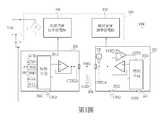
請參照第1圖,第1圖是本發明的第一實施例所公開的一種應用於電源轉換器100的主控制器(master controller)202和從控制器(slave controller)204的示意圖。如第1圖所示,電源轉換器100包含一脈波寬度調變(pulse width modulation, PWM)級電路102和一功率因素校正(power factor correction, PFC)級電路104,其中脈波寬度調變級電路102可為一返馳式(flyback)電路或一電感-電感-電容諧振電路(LLC resonant circuit),脈波寬度調變級電路102是用以轉換一交流電壓VAC為一直流電壓VDC,以及功率因素校正級電路104是用以提升電源轉換器100的轉換效率。另外,脈波寬度調變級電路102以及功率因素校正級電路104為本發明領域具有熟知技藝者所熟知,所以在此不再另行贅述。另外,如第1圖所示,主控制器202是用以控制脈波寬度調變級電路102的運作,從控制器204是用以控制功率因素校正級電路104的運作,以及主控制器202和從控制器204是分別利用接腳CTRLA、CTRLB互相溝通。另外,為了簡化第1圖,第1圖省略了主控制器202的接腳CTRLA、用以接地端GND的接腳2022以及一接腳HV外的接腳,以及也省略了從控制器204的接腳CTRLB和其用以接地端GND的接腳2042外的接腳。Please refer to FIG. 1, which is a schematic diagram of a
請參照第2圖,第2圖是本發明的第二實施例所公開的一種應用於電源轉換器的主控制器和從控制器之間的收發指令方法的流程圖。第2圖的操作方法是利用第1圖的電源轉換器100、主控制器202和從控制器204說明,詳細步驟如下:Please refer to FIG. 2. FIG. 2 is a flowchart of a method for sending and receiving commands between a master controller and a slave controller disclosed in a second embodiment of the present invention. The operation method of FIG. 2 is described using the
步驟300: 開始;Step 300: Start;
步驟302: 啟動主控制器202和從控制器204;Step 302: Start the
步驟304: 主控制器202和從控制器204中的一控制器偵測該控制器的一接腳上的節點電壓VNO;Step 304: A controller in the
步驟306: 節點電壓VNO是否小於一預定電壓VP;如果是,進行步驟308;如果否,跳至步驟316;Step 306: Whether the node voltage VNO is less than a predetermined voltage VP; if yes, proceed to
步驟308: 該控制器是否要通過該接腳傳送複數個第一指令中的一第一指令至主控制器202和從控制器204中的另一控制器;如果是,進行步驟310;如果否,跳至步驟304;Step 308: Whether the controller is to transmit a first command of the plurality of first commands to another controller of the
步驟310: 該控制器進入一發射機狀態(transmitter state);Step 310: The controller enters a transmitter state (transmitter state);
步驟312: 該控制器通過該接腳傳送該第一指令至該另一控制器;Step 312: The controller transmits the first command to the other controller through the pin;
步驟314: 該控制器是否接收到該另一控制器所傳送的第一回傳信號;如果是,跳至步驟304;如果否,跳至步驟312;Step 314: Whether the controller receives the first return signal transmitted by the other controller; if yes, skip to
步驟316: 該控制器進入一接收機狀態(receiver state);Step 316: The controller enters a receiver state (receiver state);
步驟318: 該控制器接收該另一控制器所傳送的複數個第二指令中的一第二指令,以及該控制器執行該第二指令且通過該接腳傳送一第二回傳信號至該另一控制器,跳至步驟304。Step 318: The controller receives a second command from the plurality of second commands sent by the other controller, and the controller executes the second command and sends a second return signal to the terminal through the pin The other controller skips to
首先,以該控制器為主控制器202以及該另一控制器為從控制器204為例,詳細說明如下:First, taking the controller as the
在步驟302中,在一交流電源(未繪示於第1圖)開始提供交流電壓VAC後,當交流電壓VAC大於一過壓電壓VACBNI時,主控制器202可先啟動。如第1圖所示,因為節點電壓VNO可由預定電壓VP和一熱敏電阻106(具有負溫度係數)決定,所以節點電壓VNO應小於預定電壓VP (例如1.5V)。在步驟304中,主控制器202先偵測接腳CTRLA上的節點電壓VNO並判斷是否對電源轉換器100執行一過溫度保護(over temperature protection, OTP),其中因為節點電壓VNO和預定電壓VP有關,所以預定電壓VP也和該過溫度保護有關。因此,當節點電壓VNO小於一過溫度保護參考電壓VOTP(其中過溫度保護參考電壓VOTP小於預定電壓VP,例如過溫度保護參考電壓VOTP為0.9V)時,主控制器202會產生一過溫度保護信號OTPS至主控制器202內的控制介面2024。此時,控制介面2024將會傳送過溫度保護信號OTPS至主控制器202內對應過溫度保護信號OTPS的過溫度保護電路,以及該過溫度保護電路將據以對電源轉換器100執行該過溫度保護。另外,當節點電壓VNO介於預定電壓VP和過溫度保護參考電壓VOTP時,主控制器202並不會產生過溫度保護信號OTPS至主控制器202內的控制介面2024。另外,因為該過溫度保護電路並非本發明的技術特徵,所以在此不再另行贅述。在步驟306中,在主控制器202未對電源轉換器100執行該過溫度保護後,主控制器202會偵測節點電壓VNO是否也小於預定電壓VP,其中當沒有任何指令在主控制器202和從控制器204之間傳送時,節點電壓VNO會小於預定電壓VP。在步驟308中,當節點電壓VNO小於預定電壓VP,但主控制器202不要傳送該第一指令至從控制器204時,主控制器202會再次執行步驟304繼續偵測節點電壓VNO。在步驟310中,當節點電壓VNO小於預定電壓VP且主控制器202要傳送該第一指令至從控制器204時,主控制器202進入一發射機狀態,此時,從控制器204進入一接收機狀態,且節點電壓VNO將會隨該第一指令對應地增加。在步驟314中,在從控制器204接收並執行該第一指令後,從控制器204應該要發出一第一回傳信號並通過接腳CTRLB傳送該第一回傳信號至主控制器202,其中該第一回傳信號是對應該第一指令的一信號。因此,當主控制器202未接收到該第一回傳信號時,主控制器202會再次執行步驟312以傳送該第一指令至從控制器204,以及當主控制器202接收到該第一回傳信號時,主控制器202會再次執行步驟304繼續偵測節點電壓VNO。另外,在步驟316中,當節點電壓VNO大於預定電壓VP時,意味著從控制器204傳送該第二指令至主控制器202,所以此時從控制器204進入該發射機狀態,主控制器202進入該接收機狀態,以及節點電壓VNO也將會隨該第二指令對應地增加。在步驟318中,主控制器202接收從控制器204所傳送的該第二指令,以及主控制器202執行該第二指令且通過接腳CTRLA傳送一第二回傳信號至從控制器204,其中該第二回傳信號是對應該第二指令的一信號。另外,在主控制器202執行該第二指令且通過接腳CTRLA傳送該第二回傳信號至從控制器204後,主控制器202會再次執行步驟304繼續偵測節點電壓VNO。In
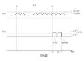
另外,請參照第3圖,第3圖是說明主控制器202和從控制器204之間的收發指令方法的時序的示意圖,其中第3圖是以該控制器為主控制器202以及該另一控制器為從控制器204為例。如第3圖所示,在一時間T1,當節點電壓VNO介於預定電壓VP和過溫度保護參考電壓VOTP時(此時意味著沒有任何指令在主控制器202和從控制器204之間傳送以及主控制器202沒有對電源轉換器100執行該過溫度保護),主控制器202可傳送該第一指令至從控制器204,其中主控制器202進入該發射機狀態,從控制器204進入該接收機狀態,節點電壓VNO將會隨該第一指令對應地增加至一對應電壓VCT(例如當該第一指令為高交流電壓指令ACHL時,對應電壓VCT將會介於4.2V~4.7V),且該第一指令的致能期間為120μs。但本發明並不受限於該第一指令的致能期間為120μs。在從控制器204接收該第一指令60μs後,從控制器204在一時間T2開始執行該第一指令。另外,如第3圖所示,在一時間T3,在從控制器204執行該第一指令後120μs,從控制器204傳送該第一回傳信號至主控制器202,其中該第一回傳信號的致能期間為120μs。但本發明並不受限於該第一回傳信號的致能期間為120μs。另外,因為該第一回傳信號是對應該第一指令,所以在該第一回傳信號的致能期間,節點電壓VNO也會隨該第一回傳信號對應地增加至對應電壓VCT。另外,如第3圖所示,在主控制器202傳送該第一指令至從控制器204後240μs(一時間T5)還未接收到該第一回傳信號時,主控制器202可在時間T5再次傳送該第一指令至從控制器204。如第3圖所示,該第一回傳信號的致能期間結束後120μs(一時間T6),如果沒有任何指令在主控制器202和從控制器204之間傳送且從控制器204想要傳送該第二指令至主控制器202時,則從控制器204可進入該發射機狀態以傳送該第二指令至主控制器202。另外,如第3圖所示,當主控制器202開始接收該第一回傳信號300μs後(一時間T7),如果沒有任何指令在主控制器202和從控制器204之間傳送且主控制器202想要傳送該第一指令或另一第一指令至從控制器204時,則主控制器202可再次進入該發射機狀態以傳送該第一指令或該另一第一指令至主控制器202。另外,本發明並不受限於第3圖所述的主控制器202和從控制器204之間的收發指令方法的時序,也就是說只要該複數個第一指令和該複數個第二指令中的每一指令對應一預定電壓範圍且主控制器202可通過接腳CTRLA執行至少一預定功能(例如該過溫度保護)都落入本發明的範疇。另外,該第一指令的致能期間的長度和該第一回傳信號的致能期間的長度可相同或不同。In addition, please refer to FIG. 3, FIG. 3 is a schematic diagram illustrating the timing of the command sending and receiving method between the
另外,該複數個第一指令和該複數個第二指令中的每一指令對應一預定電壓範圍。例如當該複數個第一指令為一交流電壓過壓(AC brown-in)指令ACBI,一交流電壓欠壓(AC brown-out)指令ACBO,一進入突發模式(PFC burst mode in)指令PFCBMI,一離開突發模式(PFC burst mode out)指令PFCBMO,一低交流電壓(AC low line)指令ACLL,以及一高交流電壓(AC high line)指令ACHL時,交流電壓過壓指令ACBI,交流電壓欠壓指令ACBO,進入突發模式指令PFCBMI,離開突發模式指令PFCBMO,低交流電壓ACLL,以及高交流電壓指令ACHL分別對應1.7V~2.2V,2.2V~2.7V,2.7V~3.2V,3.2V~3.7V,3.7V~4.2V,4.2V~4.7V,其中交流電壓過壓指令ACBI,交流電壓欠壓指令ACBO,進入突發模式指令PFCBMI,離開突發模式指令PFCBMO,低交流電壓ACLL,以及高交流電壓指令ACHL是通過主控制器202的控制介面2024和接腳CTRLA傳送至從控制器204。因此,從控制器204的控制介面2042通過接腳CTRLB接收交流電壓過壓指令ACBI,交流電壓欠壓指令ACBO,低交流電壓ACLL,以及高交流電壓指令ACHL後,控制介面2042將會傳送交流電壓過壓指令ACBI,交流電壓欠壓指令ACBO,低交流電壓ACLL,以及高交流電壓指令ACHL至控制介面2042內相對應的電路。另外,本發明並不受限於該複數個第一指令為交流電壓過壓指令ACBI,交流電壓欠壓指令ACBO,進入突發模式指令PFCBMI以及離開突發模式指令PFCBMO,低交流電壓ACLL,以及高交流電壓指令ACHL,以及也不受限於上述交流電壓過壓指令ACBI,交流電壓欠壓指令ACBO,進入突發模式指令PFCBMI以及離開突發模式指令PFCBMO,低交流電壓ACLL,以及高交流電壓指令ACHL所對應的預定電壓範圍。另外,該複數個第二指令的原理可參照上述該複數個第一指令的相關說明,在此不再贅述。In addition, each of the plurality of first instructions and the plurality of second instructions corresponds to a predetermined voltage range. For example, when the plurality of first commands are an AC brown-in command ACBI, an AC brown-out command ACBO, and a PFC burst mode in command PFCBMI , When leaving the burst mode (PFC burst mode out) command PFCBMO, a low AC voltage (AC low line) command ACLL, and a high AC voltage (AC high line) command ACHL, the AC voltage overvoltage command ACBI, AC voltage Undervoltage command ACBO, enter burst mode command PFCBMI, leave burst mode command PFCBMO, low AC voltage ACLL, and high AC voltage command ACHL correspond to 1.7V~2.2V, 2.2V~2.7V, 2.7V~3.2V, 3.2V~3.7V, 3.7V~4.2V, 4.2V~4.7V, including AC voltage overvoltage command ACBI, AC voltage undervoltage command ACBO, enter burst mode command PFCBMI, leave burst mode command PFCBMO, low AC voltage The ACLL and the high AC voltage command ACHL are transmitted to the
另外,在本發明的另一實施例中,第2圖也可以以該控制器為從控制器204以及該另一控制器為主控制器202為例,詳細說明如下:In addition, in another embodiment of the present invention, FIG. 2 may also take the controller as the
在步驟302中,從控制器204啟動。另外,因為該過溫度保護是由主控制器202所執行,所以從控制器204將會省略步驟304直接執行步驟306。在步驟306中,在主控制器202未對電源轉換器100執行該過溫度保護後,從控制器204會偵測節點電壓VNO是否也小於預定電壓VP,其中沒有任何指令在主控制器202和從控制器204之間傳送時,節點電壓VNO會小於預定電壓VP。在步驟308中,當節點電壓VNO小於預定電壓VP,但從控制器204不要傳送該第一指令至主控制器202時,從控制器204再次執行步驟306繼續偵測節點電壓VNO。在步驟310中,當節點電壓VNO小於預定電壓VP且從控制器204要傳送該第一指令至主控制器202時,從控制器204進入該發射機狀態,此時,主控制器202進入該接收機狀態,且節點電壓VNO將會隨該第一指令對應地增加。在步驟314中,在主控制器202接收並執行該第一指令後,主控制器202應該要發出該第一回傳信號並通過接腳CTRLA傳送該第一回傳信號至從控制器204。因此,當從控制器204未接收到該第一回傳信號時,從控制器204會再次執行步驟312以傳送該第一指令至主控制器202,以及當從控制器204接收到該第一回傳信號時,從控制器204再次執行步驟306繼續偵測節點電壓VNO。另外,在步驟316中,當節點電壓VNO大於預定電壓VP時,意味著主控制器202傳送該第二指令至從控制器204,所以此時主控制器202進入該發射機狀態,從控制器204進入該接收機狀態,以及節點電壓VNO也將會隨該第二指令對應地增加。在步驟318中,從控制器204接收主控制器202所傳送的該第二指令,以及從控制器204執行該第二指令且通過接腳CTRLB傳送該第二回傳信號至主控制器202。另外,在從控制器204執行該第二指令且通過接腳CTRLB傳送該第二回傳信號至主控制器202後,從控制器204再次執行步驟306繼續偵測節點電壓VNO。In
另外,請參照第4-6圖,第4圖是說明上述收發指令方法應用在電源轉換器100啟動的示意圖,第5圖是說明上述收發指令方法應用在高低交流電壓(AC high/low line)的示意圖,以及第6圖是說明上述收發指令方法應用在電源轉換器100關閉的示意圖。如第4圖所示,當該交流電源(未繪示於第1圖)開始提供交流電壓VAC時,主控制器202的接腳HV上的直流電壓VHV可隨交流電壓VAC對應地改變。因此,當直流電壓VHV大於過壓電壓VACBNI(在一時間T1)時,主控制器202內的相關電路會產生交流電壓過壓(AC brown-in)指令ACBI並通過接腳CTRLA、CTRLB傳送至從控制器204使從控制器204控制功率因素校正級電路104開始根據交流電壓過壓指令ACBI運作。如第4圖所示,節點電壓VNO將會隨交流電壓過壓指令ACBI對應地增加至一對應電壓VCT1(1.7V~2.2V),以及在一時間T2,從控制器204傳送對應交流電壓過壓指令ACBI的回傳信號RACBI至主控制器202,其中在回傳信號RACBI的致能期間(時間T2-時間T3),節點電壓VNO也會隨回傳信號RACBI對應地增加至對應電壓VCT1。In addition, please refer to FIGS. 4-6. FIG. 4 is a schematic diagram illustrating the application of the above-mentioned sending and receiving command method to the startup of the
因為直流電壓VHV可隨交流電壓VAC對應地改變,所以當交流電壓VAC增加時,直流電壓VHV也會對應地增加,以及當交流電壓VAC降低時,直流電壓VHV也會對應地降低。因此,如第5圖所示,在一時間T1後,直流電壓VHV開始交越一高交流電壓參考電壓VACHL,所以主控制器202內的相關電路會在一時間T2產生高交流電壓(AC high line)指令ACHL並通過接腳CTRLA、CTRLB傳送至從控制器204使從控制器204控制功率因素校正級電路104開始根據高交流電壓指令ACHL運作,其中一延遲時間TD1介於時間T1與時間T2之間。如第5圖所示,節點電壓VNO將會隨高交流電壓指令ACHL對應地增加至一對應電壓VCT2(4.2V~4.7V),以及在一時間T3,從控制器204傳送對應高交流電壓指令ACHL的回傳信號RACHL至主控制器202,其中在回傳信號RACHL的致能期間(時間T3-時間T4),節點電壓VNO也會隨回傳信號RACHL對應地增加至對應電壓VCT2。如第5圖所示,在一時間T5後,直流電壓VHV開始小於一低交流電壓參考電壓VACLL,所以主控制器202內的相關電路會在一時間T6產生低交流電壓(AC low line)指令ACLL並通過接腳CTRLA、CTRLB傳送至從控制器204使從控制器204控制功率因素校正級電路104開始根據低交流電壓指令ACLL運作,其中一延遲時間TD2介於時間T5與時間T6之間,且延遲時間TD1和延遲時間TD2可相同或不同。如第5圖所示,節點電壓VNO將會隨低交流電壓指令ACLL對應地增加至一對應電壓VCT3(3.7V~4.2V),以及在一時間T7,從控制器204傳送對應低交流電壓指令ACLL的回傳信號RACLL至主控制器202,其中在回傳信號RACLL的致能期間(時間T7-時間T8),節點電壓VNO也會隨回傳信號RACLL對應地增加至對應電壓VCT3。Since the DC voltage VHV can be changed correspondingly with the AC voltage VAC, when the AC voltage VAC increases, the DC voltage VHV also correspondingly increases, and when the AC voltage VAC decreases, the DC voltage VHV also correspondingly decreases. Therefore, as shown in FIG. 5, after a time T1, the DC voltage VHV starts to cross a high AC voltage reference voltage VACHL, so the related circuits in the
另外,如第6圖所示,當直流電壓VHV小於欠壓電壓VACBNO一延遲時間TD3後,主控制器202內的相關電路將在一時間T1產生交流電壓欠壓(AC brown-out)指令ACBO並通過接腳CTRLA、CTRLB傳送至從控制器204使從控制器204控制功率因素校正級電路104開始根據交流電壓欠壓指令ACBO關閉。如第6圖所示,節點電壓VNO將會隨交流電壓欠壓指令ACBO對應地增加至一對應電壓VCT4(2.2V~2.7V),以及在一時間T2,從控制器204傳送對應交流電壓欠壓指令ACBO的回傳信號RACBO至主控制器202,其中在回傳信號RACBO的致能期間(時間T2-時間T3),節點電壓VNO也會隨回傳信號RACBO對應地增加至對應電壓VCT4。In addition, as shown in FIG. 6, when the DC voltage VHV is less than the undervoltage VACBNO for a delay time TD3, the relevant circuit in the
綜上所述,本發明所提供的收發指令方法是將該主控制器與該從控制器之間傳輸的複數個指令中的每一指令對應一預定電壓範圍,且該主控制器用以傳輸該複數個指令的接腳是對應至少一預定功能(例如該過溫度保護)。因此,相較於現有技術,本發明所提供的收發指令方法同時具有運作簡單,涵蓋多個指令,且該主控制器與該從控制器都不需額外接腳以執行本發明的優點。 以上所述僅為本發明之較佳實施例,凡依本發明申請專利範圍所做之均等變化與修飾,皆應屬本發明之涵蓋範圍。In summary, the method for sending and receiving commands provided by the present invention is to correspond to each of a plurality of commands transmitted between the master controller and the slave controller to a predetermined voltage range, and the master controller is used to transmit the The pins of the plurality of instructions correspond to at least one predetermined function (such as the over-temperature protection). Therefore, compared to the prior art, the method for sending and receiving commands provided by the present invention has simple operation and covers multiple commands, and neither the master controller nor the slave controller needs extra pins to perform the advantages of the present invention. The above are only the preferred embodiments of the present invention, and all changes and modifications made in accordance with the scope of the patent application of the present invention shall fall within the scope of the present invention.
100:電源轉換器102:脈波寬度調變級電路104:功率因素校正級電路106:熱敏電阻202:主控制器204:從控制器2022、2042、CTRLA、CTRLB、HV:接腳2024、2042:控制介面ACBI:交流電壓過壓指令ACBO:交流電壓欠壓指令ACHL:高交流電壓指令ACLL:低交流電壓指令GND:地端OTPS:過溫度保護信號PFCBMI:進入突發模式指令PFCBMO:離開突發模式指令RACBI、RACHL、RACLL、RACBO:回傳信號T1-T7:時間TD1、TD2、TD3:延遲時間VCT、VCT1、VCT2、VCT3:對應電壓VAC:交流電壓VDC:直流電壓VNO:節點電壓VP:預定電壓VOTP:過溫度保護參考電壓VACBNI:過壓電壓VACBNO:欠壓電壓VACHL:高交流電壓參考電壓VACLL:低交流電壓參考電壓300-318:步驟100: power converter102: Pulse width modulation stage circuit104: Power factor correction stage circuit106: Thermistor202: main controller204:
第1圖是本發明的第一實施例所公開的一種應用於電源轉換器的主控制器和從控制器的示意圖。 第2圖是本發明的第二實施例所公開的一種應用於電源轉換器的主控制器和從控制器之間的收發指令方法的流程圖。 第3圖是說明主控制器和從控制器之間的收發指令方法的時序的示意圖。 第4圖是說明上述收發指令方法應用在電源轉換器100啟動的示意圖。 第5圖是說明上述收發指令方法應用在高低交流電壓(AC high/low line)的示意圖。 第6圖是說明上述收發指令方法應用在電源轉換器100關閉的示意圖。FIG. 1 is a schematic diagram of a master controller and a slave controller applied to a power converter disclosed in the first embodiment of the present invention. FIG. 2 is a flowchart of a method for sending and receiving instructions between a master controller and a slave controller disclosed in a second embodiment of the present invention. FIG. 3 is a schematic diagram illustrating the timing of the command transmission and reception method between the master controller and the slave controller. FIG. 4 is a schematic diagram illustrating the application of the above method for sending and receiving commands to the
300-318:步驟300-318: steps
Claims (14)
Translated fromChinesePriority Applications (2)
| Application Number | Priority Date | Filing Date | Title |
|---|---|---|---|
| TW108113697ATWI691844B (en) | 2019-04-19 | 2019-04-19 | Transmitting/receiving command method applied between a master controller and a slave controller of a power converter |
| US16/594,058US10848055B2 (en) | 2019-04-19 | 2019-10-06 | Transmitting/receiving command method applied between a master controller and a slave controller of a power converter |
Applications Claiming Priority (1)
| Application Number | Priority Date | Filing Date | Title |
|---|---|---|---|
| TW108113697ATWI691844B (en) | 2019-04-19 | 2019-04-19 | Transmitting/receiving command method applied between a master controller and a slave controller of a power converter |
Publications (2)
| Publication Number | Publication Date |
|---|---|
| TWI691844Btrue TWI691844B (en) | 2020-04-21 |
| TW202040371A TW202040371A (en) | 2020-11-01 |
Family
ID=71134485
Family Applications (1)
| Application Number | Title | Priority Date | Filing Date |
|---|---|---|---|
| TW108113697ATWI691844B (en) | 2019-04-19 | 2019-04-19 | Transmitting/receiving command method applied between a master controller and a slave controller of a power converter |
Country Status (2)
| Country | Link |
|---|---|
| US (1) | US10848055B2 (en) |
| TW (1) | TWI691844B (en) |
Families Citing this family (3)
| Publication number | Priority date | Publication date | Assignee | Title |
|---|---|---|---|---|
| CN111525514B (en)* | 2019-02-01 | 2023-02-28 | 群光电能科技股份有限公司 | Power Converter with Over-Temperature Protection Compensation |
| CN113922647B (en)* | 2019-02-01 | 2024-11-15 | 群光电能科技股份有限公司 | Power converter with over temperature protection compensation |
| TWI717247B (en)* | 2020-03-30 | 2021-01-21 | 通嘉科技股份有限公司 | Power controller and control method for llc resonant converter |
Citations (5)
| Publication number | Priority date | Publication date | Assignee | Title |
|---|---|---|---|---|
| TWI487255B (en)* | 2012-07-13 | 2015-06-01 | Power Forest Technology Corp | Flyback-based power conversion apparatus and power conversion method thereof |
| TWI493849B (en)* | 2013-09-06 | 2015-07-21 | Leadtrend Tech Corp | Power supplies and control methods capable of improving power factor during light load |
| US9906145B2 (en)* | 2016-06-16 | 2018-02-27 | Nxp B.V. | Power converter with load switch fault protection |
| US20180123448A1 (en)* | 2010-12-08 | 2018-05-03 | On-Bright Electronics (Shanghai) Co., Ltd. | System and method providing over current protection based on duty cycle information for power converter |
| CN207926460U (en)* | 2018-02-06 | 2018-09-28 | 苏州力生美半导体有限公司 | Non-isolated single-chip AC/DC switching power source control circuits |
Family Cites Families (2)
| Publication number | Priority date | Publication date | Assignee | Title |
|---|---|---|---|---|
| KR102210890B1 (en)* | 2013-06-05 | 2021-02-02 | 삼성에스디아이 주식회사 | Battery management system, and method of managing the same |
| KR102474424B1 (en)* | 2017-10-31 | 2022-12-05 | 주식회사 엘엑스세미콘 | Communication method between master controller and slave controller, the slave controller for the same, and battery management system using the same |
- 2019
- 2019-04-19TWTW108113697Apatent/TWI691844B/enactive
- 2019-10-06USUS16/594,058patent/US10848055B2/enactiveActive
Patent Citations (5)
| Publication number | Priority date | Publication date | Assignee | Title |
|---|---|---|---|---|
| US20180123448A1 (en)* | 2010-12-08 | 2018-05-03 | On-Bright Electronics (Shanghai) Co., Ltd. | System and method providing over current protection based on duty cycle information for power converter |
| TWI487255B (en)* | 2012-07-13 | 2015-06-01 | Power Forest Technology Corp | Flyback-based power conversion apparatus and power conversion method thereof |
| TWI493849B (en)* | 2013-09-06 | 2015-07-21 | Leadtrend Tech Corp | Power supplies and control methods capable of improving power factor during light load |
| US9906145B2 (en)* | 2016-06-16 | 2018-02-27 | Nxp B.V. | Power converter with load switch fault protection |
| CN207926460U (en)* | 2018-02-06 | 2018-09-28 | 苏州力生美半导体有限公司 | Non-isolated single-chip AC/DC switching power source control circuits |
Also Published As
| Publication number | Publication date |
|---|---|
| US20200336062A1 (en) | 2020-10-22 |
| US10848055B2 (en) | 2020-11-24 |
| TW202040371A (en) | 2020-11-01 |
Similar Documents
| Publication | Publication Date | Title |
|---|---|---|
| TWI714510B (en) | Secondary side controlled control circuit and method of forming secondary side controlled control circuit | |
| US10230303B2 (en) | Isolated switching power converter with data communication between primary and secondary sides | |
| TWI691844B (en) | Transmitting/receiving command method applied between a master controller and a slave controller of a power converter | |
| US8854842B2 (en) | Digital communication link between secondary side and primary side of switching power converter | |
| US12244169B2 (en) | Current sharing for multi-output charging device | |
| US8774254B2 (en) | Control circuit of flyback power converter with bidirectional communication channel | |
| CN105763032B (en) | Electronic device and control method thereof | |
| CN103392379A (en) | Led driver, lighting device and LED based lighting application | |
| CN105871214A (en) | System and method for secondary-side power regulation | |
| CN101002187A (en) | Method for controlling transmissions of a bi-directional interface | |
| TW201249063A (en) | Power supply system with variable supply voltage | |
| CN111835214B (en) | Method for sending and receiving commands between a master controller and a slave controller for a power converter | |
| CN110362008A (en) | A kind of High Voltage Power Supply equipment power supply electrifying sequential control circuit | |
| US20150241864A1 (en) | Zero sequence current control apparatus and method for parallel power converters | |
| TWI743916B (en) | Power conversion device, control module and method of operating the same | |
| CN115149811A (en) | Flyback converter and its startup control method | |
| TWI556565B (en) | Power supply module and control method thereof | |
| TWI858945B (en) | Power converter and method for feedback control the same | |
| TWI840292B (en) | Isolation integrated circuit, carrier frequency control circuit and modulation signal generation method | |
| CN220528016U (en) | Isolated integrated circuit and carrier frequency control circuit | |
| CN105576838A (en) | Wireless energy receiving device, wireless energy transmission system and method thereof | |
| CN108574415B (en) | Double-side voltage modulation method and converter | |
| TWM650457U (en) | Isolation integrated circuit and carrier frequency control circuit | |
| CN120150489A (en) | Control circuit and control method of isolated switching converter | |
| KR20180137995A (en) | Power supplying apparatus having power saving function and air conditioner including the same |