TWI691076B - Semiconductor structure and method of forming the same - Google Patents
Semiconductor structure and method of forming the sameDownload PDFInfo
- Publication number
- TWI691076B TWI691076BTW105124552ATW105124552ATWI691076BTW I691076 BTWI691076 BTW I691076BTW 105124552 ATW105124552 ATW 105124552ATW 105124552 ATW105124552 ATW 105124552ATW I691076 BTWI691076 BTW I691076B
- Authority
- TW
- Taiwan
- Prior art keywords
- trench
- dielectric layer
- fin
- semiconductor structure
- item
- Prior art date
Links
- 239000004065semiconductorSubstances0.000titleclaimsabstractdescription43
- 238000000034methodMethods0.000titleclaimsabstractdescription38
- 239000000758substrateSubstances0.000claimsabstractdescription20
- 238000002955isolationMethods0.000claimsabstractdescription13
- 239000002184metalSubstances0.000claimsdescription21
- 238000004519manufacturing processMethods0.000claimsdescription16
- 239000003989dielectric materialSubstances0.000claimsdescription12
- 238000000137annealingMethods0.000claimsdescription5
- 239000010410layerSubstances0.000description103
- 238000000059patterningMethods0.000description16
- VYPSYNLAJGMNEJ-UHFFFAOYSA-NSilicium dioxideChemical compoundO=[Si]=OVYPSYNLAJGMNEJ-UHFFFAOYSA-N0.000description13
- 229910052814silicon oxideInorganic materials0.000description13
- 239000011229interlayerSubstances0.000description8
- 238000005530etchingMethods0.000description7
- 229910052581Si3N4Inorganic materials0.000description5
- 239000013078crystalSubstances0.000description5
- 238000010586diagramMethods0.000description5
- 230000005669field effectEffects0.000description5
- HQVNEWCFYHHQES-UHFFFAOYSA-Nsilicon nitrideChemical compoundN12[Si]34N5[Si]62N3[Si]51N64HQVNEWCFYHHQES-UHFFFAOYSA-N0.000description5
- 230000007547defectEffects0.000description4
- 238000011161developmentMethods0.000description4
- XUIMIQQOPSSXEZ-UHFFFAOYSA-NSiliconChemical compound[Si]XUIMIQQOPSSXEZ-UHFFFAOYSA-N0.000description3
- 238000000231atomic layer depositionMethods0.000description3
- 238000009792diffusion processMethods0.000description3
- 229910052710siliconInorganic materials0.000description3
- 239000010703siliconSubstances0.000description3
- 239000000126substanceSubstances0.000description3
- 230000000694effectsEffects0.000description2
- 238000005468ion implantationMethods0.000description2
- 239000000463materialSubstances0.000description2
- 238000012986modificationMethods0.000description2
- 230000004048modificationEffects0.000description2
- 238000012546transferMethods0.000description2
- 229910021417amorphous siliconInorganic materials0.000description1
- QVGXLLKOCUKJST-UHFFFAOYSA-Natomic oxygenChemical compound[O]QVGXLLKOCUKJST-UHFFFAOYSA-N0.000description1
- 230000015572biosynthetic processEffects0.000description1
- 238000005229chemical vapour depositionMethods0.000description1
- 238000005520cutting processMethods0.000description1
- 238000000151depositionMethods0.000description1
- 238000013461designMethods0.000description1
- 238000000407epitaxyMethods0.000description1
- 230000009969flowable effectEffects0.000description1
- 239000011810insulating materialSubstances0.000description1
- 238000009413insulationMethods0.000description1
- 239000012212insulatorSubstances0.000description1
- 230000003287optical effectEffects0.000description1
- 230000003647oxidationEffects0.000description1
- 238000007254oxidation reactionMethods0.000description1
- 229910052760oxygenInorganic materials0.000description1
- 239000001301oxygenSubstances0.000description1
- 238000005498polishingMethods0.000description1
- 229910021420polycrystalline siliconInorganic materials0.000description1
- 229920005591polysiliconPolymers0.000description1
Images


Classifications
- H—ELECTRICITY
- H10—SEMICONDUCTOR DEVICES; ELECTRIC SOLID-STATE DEVICES NOT OTHERWISE PROVIDED FOR
- H10D—INORGANIC ELECTRIC SEMICONDUCTOR DEVICES
- H10D62/00—Semiconductor bodies, or regions thereof, of devices having potential barriers
- H10D62/10—Shapes, relative sizes or dispositions of the regions of the semiconductor bodies; Shapes of the semiconductor bodies
- H10D62/113—Isolations within a component, i.e. internal isolations
- H10D62/115—Dielectric isolations, e.g. air gaps
- H10D62/116—Dielectric isolations, e.g. air gaps adjoining the input or output regions of field-effect devices, e.g. adjoining source or drain regions
- H—ELECTRICITY
- H01—ELECTRIC ELEMENTS
- H01L—SEMICONDUCTOR DEVICES NOT COVERED BY CLASS H10
- H01L21/00—Processes or apparatus adapted for the manufacture or treatment of semiconductor or solid state devices or of parts thereof
- H01L21/70—Manufacture or treatment of devices consisting of a plurality of solid state components formed in or on a common substrate or of parts thereof; Manufacture of integrated circuit devices or of parts thereof
- H01L21/71—Manufacture of specific parts of devices defined in group H01L21/70
- H01L21/76—Making of isolation regions between components
- H01L21/762—Dielectric regions, e.g. EPIC dielectric isolation, LOCOS; Trench refilling techniques, SOI technology, use of channel stoppers
- H01L21/76224—Dielectric regions, e.g. EPIC dielectric isolation, LOCOS; Trench refilling techniques, SOI technology, use of channel stoppers using trench refilling with dielectric materials
- H—ELECTRICITY
- H10—SEMICONDUCTOR DEVICES; ELECTRIC SOLID-STATE DEVICES NOT OTHERWISE PROVIDED FOR
- H10D—INORGANIC ELECTRIC SEMICONDUCTOR DEVICES
- H10D30/00—Field-effect transistors [FET]
- H10D30/01—Manufacture or treatment
- H10D30/021—Manufacture or treatment of FETs having insulated gates [IGFET]
- H10D30/024—Manufacture or treatment of FETs having insulated gates [IGFET] of fin field-effect transistors [FinFET]
- H—ELECTRICITY
- H10—SEMICONDUCTOR DEVICES; ELECTRIC SOLID-STATE DEVICES NOT OTHERWISE PROVIDED FOR
- H10D—INORGANIC ELECTRIC SEMICONDUCTOR DEVICES
- H10D30/00—Field-effect transistors [FET]
- H10D30/60—Insulated-gate field-effect transistors [IGFET]
- H10D30/62—Fin field-effect transistors [FinFET]
- H10D30/6211—Fin field-effect transistors [FinFET] having fin-shaped semiconductor bodies integral with the bulk semiconductor substrates
- H—ELECTRICITY
- H10—SEMICONDUCTOR DEVICES; ELECTRIC SOLID-STATE DEVICES NOT OTHERWISE PROVIDED FOR
- H10D—INORGANIC ELECTRIC SEMICONDUCTOR DEVICES
- H10D84/00—Integrated devices formed in or on semiconductor substrates that comprise only semiconducting layers, e.g. on Si wafers or on GaAs-on-Si wafers
- H10D84/01—Manufacture or treatment
- H10D84/0123—Integrating together multiple components covered by H10D12/00 or H10D30/00, e.g. integrating multiple IGBTs
- H10D84/0126—Integrating together multiple components covered by H10D12/00 or H10D30/00, e.g. integrating multiple IGBTs the components including insulated gates, e.g. IGFETs
- H10D84/0151—Manufacturing their isolation regions
- H—ELECTRICITY
- H10—SEMICONDUCTOR DEVICES; ELECTRIC SOLID-STATE DEVICES NOT OTHERWISE PROVIDED FOR
- H10D—INORGANIC ELECTRIC SEMICONDUCTOR DEVICES
- H10D84/00—Integrated devices formed in or on semiconductor substrates that comprise only semiconducting layers, e.g. on Si wafers or on GaAs-on-Si wafers
- H10D84/01—Manufacture or treatment
- H10D84/0123—Integrating together multiple components covered by H10D12/00 or H10D30/00, e.g. integrating multiple IGBTs
- H10D84/0126—Integrating together multiple components covered by H10D12/00 or H10D30/00, e.g. integrating multiple IGBTs the components including insulated gates, e.g. IGFETs
- H10D84/0158—Integrating together multiple components covered by H10D12/00 or H10D30/00, e.g. integrating multiple IGBTs the components including insulated gates, e.g. IGFETs the components including FinFETs
- H—ELECTRICITY
- H10—SEMICONDUCTOR DEVICES; ELECTRIC SOLID-STATE DEVICES NOT OTHERWISE PROVIDED FOR
- H10D—INORGANIC ELECTRIC SEMICONDUCTOR DEVICES
- H10D84/00—Integrated devices formed in or on semiconductor substrates that comprise only semiconducting layers, e.g. on Si wafers or on GaAs-on-Si wafers
- H10D84/01—Manufacture or treatment
- H10D84/02—Manufacture or treatment characterised by using material-based technologies
- H10D84/03—Manufacture or treatment characterised by using material-based technologies using Group IV technology, e.g. silicon technology or silicon-carbide [SiC] technology
- H10D84/038—Manufacture or treatment characterised by using material-based technologies using Group IV technology, e.g. silicon technology or silicon-carbide [SiC] technology using silicon technology, e.g. SiGe
Landscapes
- Engineering & Computer Science (AREA)
- Physics & Mathematics (AREA)
- Condensed Matter Physics & Semiconductors (AREA)
- General Physics & Mathematics (AREA)
- Manufacturing & Machinery (AREA)
- Computer Hardware Design (AREA)
- Microelectronics & Electronic Packaging (AREA)
- Power Engineering (AREA)
- Insulated Gate Type Field-Effect Transistor (AREA)
Abstract
Description
Translated fromChinese本發明是關於一種半導體結構及其製作方法,特別是一種半導體結構的隔離結構及其製作方法。The invention relates to a semiconductor structure and a manufacturing method thereof, in particular to an isolation structure of a semiconductor structure and a manufacturing method thereof.
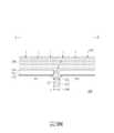
先進半導體技術中,鰭狀場效電晶體(fin field effect transistor,Fin FET)已取代平面式(planar)場效電晶體,成為主流發展趨勢。一般而言,製作鰭狀場效電晶體的第一步,是利用例如顯影暨蝕刻製程(photolithograph-etching process,PEP)等圖案化製程,根據布局圖案,在半導體基底上形成溝渠以定義出鰭狀結構(fin structure)。接著,再於溝渠中填入絕緣材料,完成各鰭狀結構之間的絕緣。後續,形成跨越鰭狀結構的閘極,被閘極覆蓋的鰭狀結構區域,即為元件的通道區。為了增加元件效能,會於閘極兩側的鰭狀結構中形成應變矽(strained silicon),作為元件的源/汲極區。隨著元件尺寸的微縮,鰭狀結構的尺寸和彼此的間隙(pitch)也越來小。為了得到更好的顯影解析度並減少蝕刻負載效應而導致的變形,多重圖案化(multiple patterning)技術,例如顯影-蝕刻-顯影-蝕刻(photolithography-etch-photolithography-etch,2P2E)、顯影-顯影-蝕刻(photolithography-photolithography-etch,2P1E)或側壁子自對準雙圖案法(spacer self-aligned double-patterning,SADP)等,已被提出並且被廣泛利用。例如,如第1圖所示,先利用第一次圖案化,在基底1中定義出鰭狀結構陣列10,其中包含複數條往同一方向延伸並且緊密排列的鰭狀結構,彼此之間由溝渠20隔離。然後進行第二次圖案化,例如移除部分虛置鰭狀結構10a和10b,形成較大尺寸的溝渠21。再利用第三次圖案化,例如形成溝渠22、24、26,以將連續的鰭狀結構區分成不連續的區段(或區塊)。經過上述過程將鰭狀結構陣列10區分成所需的區段(或區塊)後,再將介電材料填入溝渠20、21、22、24、26中並進行平坦化,形成隔離結構。藉由上述多重圖案化方法形成的鰭狀結構,具有較均勻的尺寸以及平整的剖面形狀,因此較不易受光學鄰近效應(optical proximity effect,OPE)而產生變窄或退縮的端點,或者圖案密度不同時仍可具有相近的剖面輪廓。In advanced semiconductor technology, fin field effect transistors (Fin FETs) have replaced planar field effect transistors and become the mainstream development trend. Generally speaking, the first step in the fabrication of fin field effect transistors is to use a patterning process such as a photolithograph-etching process (PEP) to form trenches on the semiconductor substrate according to the layout pattern to define fins Fin structure. Then, the trench is filled with insulating material to complete the insulation between the fin structures. Subsequently, a gate electrode spanning the fin structure is formed, and the fin structure region covered by the gate electrode is the channel region of the device. In order to increase the device performance, strained silicon is formed in the fin structures on both sides of the gate as the source/drain regions of the device. As the size of the device shrinks, the size of the fin structure and the pitch between each other become smaller. In order to obtain better development resolution and reduce the deformation caused by the etching load effect, multiple patterning (multiple patterning) technology, such as development-etch-development-etch (photolithography-etch-photolithography-etch, 2P2E), development-development -Etching (photolithography-photolithography-etch, 2P1E) or sidewall self-aligned double-patterning (SADP), etc., have been proposed and widely used. For example, as shown in FIG. 1, the first patterning is first used to define a fin-
然而,為了實現較緊密的布局,溝渠的寬度可能越來越小。對於用來切斷連續鰭狀結構的溝渠24,越小的寬度使得相對的端點,例如10c和10d,更加靠近,導製後續成長於端點的磊晶容易橋接在一起,造成位於溝渠24兩側的元件發生短路。另外,同樣為了實現較緊密的布局,源/汲極接觸插塞(S/D contact)的位置可能更靠近鰭狀結構的端點,但端點的磊晶常存在晶面缺陷(facet defect),導致與源/汲極接觸插塞之間的不良接觸。However, in order to achieve a tighter layout, the width of the trench may become smaller and smaller. For the
因此,本領域仍需要一種改良的的隔離結構,用於將連續的鰭狀結構區分成數個區段,不僅具有較小的寬度以實現較緊密的布局,還可避免鰭狀結構端點的磊晶橋接以及改善位於端點的接觸插塞的良率。Therefore, there is still a need in the art for an improved isolation structure for dividing a continuous fin-like structure into several sections, which not only has a smaller width to achieve a tighter layout, but also avoids the end points of the fin-like structure Crystal bridging and improving the yield of contact plugs at the end points.
本發明一方面提供一種半導體結構,包含一鰭狀結構,位於一基底上。一隔離結構,位於該鰭狀結構中,該隔離結構包含一溝渠,包含一圓化的頂角,一上部,具有凹面的上側壁,一下部,具有筆直的下側壁。一第一介電層,填充該溝渠的該下部並且具有一凹面的上表面。一高介電常數介電層,覆蓋該溝渠的該上側壁和該頂角,以及該第一介電層的該上表面。One aspect of the present invention provides a semiconductor structure including a fin-like structure on a substrate. An isolation structure is located in the fin structure. The isolation structure includes a trench, including a rounded apex angle, an upper portion, a concave upper side wall, and a lower portion, with a straight lower side wall. A first dielectric layer fills the lower part of the trench and has a concave upper surface. A high dielectric constant dielectric layer covers the upper sidewall and the top corner of the trench, and the upper surface of the first dielectric layer.
根據本發明一實施例,該高介電常數介電層接近該頂角的部分具有一喙狀輪廓。According to an embodiment of the present invention, a portion of the high-k dielectric layer near the vertex has a beak-shaped profile.
根據本發明另一實施例,該半導體結構另包含一閘極體,位於該鰭狀結構上,對準並完全覆蓋該溝渠、一側壁子,位於該閘極體的相對兩側壁上,以及一閘極介電層,位於該側壁子與該鰭狀結構之間。其中,該閘極體填入該溝渠的該上部,其底面低於該鰭狀結構50至100埃(Å)。According to another embodiment of the present invention, the semiconductor structure further includes a gate body, located on the fin structure, aligned and completely covering the trench, a sidewall, located on opposite sidewalls of the gate body, and a The gate dielectric layer is located between the side wall and the fin structure. Wherein, the gate body is filled into the upper part of the trench, and its bottom surface is 50 to 100 angstroms (Å) lower than the fin structure.
本發明另一方面提供一種半導體結構的製作方法,步驟包含於一基底上形成一鰭狀結構,接著於該鰭狀結構中形成一溝渠,具有一頂角、一上部和一上側壁,一下部和一下側壁,然後形成一第一介電層,填充該溝渠的該下部,再形成一高介電常數介電層,覆蓋該溝渠的該頂角和該上側壁,以及該第一介電層的一上表面。其中,該溝渠的該頂角為一圓化的頂角,該上側壁為一凹面的上側壁,該下側壁為一筆直的下側壁,該第一介電層的該上表面為一凹面。Another aspect of the present invention provides a method for manufacturing a semiconductor structure. The steps include forming a fin structure on a substrate, and then forming a trench in the fin structure with a top corner, an upper portion, an upper sidewall, and a lower portion And the lower side wall, then a first dielectric layer is formed to fill the lower part of the trench, and a high dielectric constant dielectric layer is formed to cover the top corner of the trench and the upper side wall, and the first dielectric layer The upper surface of the. Wherein, the apex angle of the trench is a rounded apex angle, the upper side wall is a concave upper side wall, the lower side wall is a straight lower side wall, and the upper surface of the first dielectric layer is a concave surface.
根據本發明一實施例,該高介電常數介電層接近該頂角的部分具有一喙狀輪廓。According to an embodiment of the present invention, a portion of the high-k dielectric layer near the vertex has a beak-shaped profile.
1:基底1: base
10:鰭狀結構陣列10: Fin structure array
10a、10b:虛置鰭狀結構10a, 10b: dummy fin structure
10c、10d:端點10c, 10d: endpoint
20、21、22、24、26:溝渠20, 21, 22, 24, 26: Ditch
100:基底100: base
102、104、106:鰭狀結構102, 104, 106: Fin structure
110:鰭間溝渠110: Ditch between fins
120:溝渠120: Ditch
120a:上部120a: upper part
120b:下部120b: Lower
122、122':側壁122, 122': sidewall
124、124':頂角124, 124': vertex angle
126、126':上側壁126, 126': upper side wall
128:下側壁128: lower side wall
132:氧化矽墊層132: Silicon oxide pad
134:氮化矽墊層134: Silicon nitride pad
136:氧化矽墊層136: Silicon oxide cushion
140:第一介電材料層140: first dielectric material layer
142:退火製程142: Annealing process
144:氧化物層144: oxide layer
146:第一介電層146: first dielectric layer
148、148':上表面148, 148': upper surface
150:離子植入製程150: ion implantation process
152:井區152: Well District
160:閘極介電層160: Gate dielectric layer
162:底切162: Undercut
170、180:閘極結構170, 180: Gate structure
172、182:閘極體172, 182: Gate body
174、184:側壁子174, 184: side wall
176、186:閘極溝渠176, 186: Gate ditches
178、188:金屬閘極結構178, 188: metal gate structure
190:磊晶層190: Epitaxial layer
192:源/汲極區192: source/drain region
210:接觸蝕刻停止層210: Contact etching stop layer
220:層間介電層220: interlayer dielectric layer
310:介面層310: interface layer
320:高介電常數介電層320: High dielectric constant dielectric layer
330:金屬閘極體330: Metal gate body
230:層間介電層230: interlayer dielectric layer
410、420:接觸插塞410, 420: contact plug
w1、w2、w2'、w3:寬度w1, w2, w2', w3: width
d1、d2、d2':深度d1, d2, d2': depth
P1:間距P1: pitch
所附圖式提供對於此實施例更深入的了解,並納入此說明書成為其中一部分。這些圖式與描述,用來說明一些實施例的原理。The attached drawings provide a deeper understanding of this embodiment and are incorporated into this description as part of it. These drawings and descriptions are used to illustrate the principles of some embodiments.
第1為頂視圖,說明利用多重圖案化(multiple patterning)技術,製作鰭狀結構的區塊或區段。The first is a top view illustrating the use of multiple patterning (multiple patterning) technology to produce fin-like structure blocks or sections.
第2圖至第11圖為根據本發明一實施例,製作半導體結構的步驟示意圖,其中:第2圖為該半導體結構,於形成鰭狀結構及溝渠後的視意圖,其中,第2(a)圖為頂視圖,第2(b)圖為沿著第2(a)圖中A-A’切線的剖面示意圖,第2(c)圖為沿著第2(a)圖中B-B’切線的剖面示意圖;第3圖為該半導體結構於形成第一介電材料層的剖面示意圖;第4圖為該半導體結構於移除部分第一介電材料層以及墊層,並形成井區的剖面示意圖;第5圖為該半導體結構於形成僅填充溝渠下部的第一介電層,以及形成閘極介電層後的剖面示意圖;第6圖為該半導體結構於形成閘極結構後的示意圖,其中,第6(a)圖為頂視圖,第6(b)圖為沿著第6(a)圖中A-A’切線的剖面示意圖;第7圖為該半導體結構於形成源/汲極區後的剖面示意圖;第8圖為該半導體結構於形成接觸蝕刻停止層以及層間介電層後的剖面示意圖;第9圖為該半導體結構於形成閘極溝渠後的剖面示意圖;第10圖為該半導體結構於形成介面層、高介電常數介電層以及金屬閘極體後的剖面示意圖;以及第11圖為該半導體結構於形成接觸插塞之後的剖面示意圖。Figures 2 to 11 are schematic diagrams of steps for fabricating a semiconductor structure according to an embodiment of the present invention, in which:Figure 2 is a schematic view of the semiconductor structure after the formation of the fin structure and the trench. Figure 2(a) is a top view and Figure 2(b) is along A- in Figure 2(a). A'tangent cross-sectional schematic diagram, Figure 2(c) is a cross-sectional schematic diagram along BB' tangent line in Figure 2(a); Figure 3 is a cross-sectional schematic diagram of the semiconductor structure in forming a first dielectric material layer Figure 4 is a schematic cross-sectional view of the semiconductor structure after removing a part of the first dielectric material layer and the pad layer, and forming the well region; Figure 5 is the semiconductor structure forming the first dielectric layer that only fills the lower part of the trench, And a schematic cross-sectional view after forming the gate dielectric layer; FIG. 6 is a schematic view of the semiconductor structure after forming the gate structure, wherein FIG. 6(a) is a top view, and FIG. 6(b) is along the 6(a) is a schematic cross-sectional view taken along line AA' in FIG. 7 is a schematic cross-sectional view of the semiconductor structure after forming a source/drain region; FIG. 8 is a semiconductor structure after forming a contact etch stop layer and an interlayer A schematic cross-sectional view after an electrical layer; FIG. 9 is a schematic cross-sectional view of the semiconductor structure after forming a gate trench; FIG. 10 is a schematic view of the semiconductor structure after forming an interface layer, a high dielectric constant dielectric layer, and a metal gate body A schematic cross-sectional view; and FIG. 11 is a schematic cross-sectional view of the semiconductor structure after forming a contact plug.
在下面的描述中,已提供許多具體細節以便徹底理解本發明。然而,很明顯,對本領域技術人員而言,本發明還是可以在沒有這些具體細節的情況下實施。此外,一些公知的系統配置和製程步驟沒有被鉅細靡遺的披露出來,因為這些應是本領域技術人員所熟知的。在不悖離本發明的範圍內,可做結構、邏輯和電性上的修改應用在其他實施例上。In the following description, many specific details have been provided for a thorough understanding of the present invention. However, it is obvious to a person skilled in the art that the present invention can be implemented without these specific details. In addition, some well-known system configurations and process steps have not been disclosed in detail, because these should be well known to those skilled in the art. Without departing from the scope of the present invention, structural, logical, and electrical modifications may be applied to other embodiments.
實施例的圖式為示意圖,並未照實際比例繪製,為了清楚呈現而放大一些尺寸。在此公開和描述的多個實施例中若具有共通或類似的某些特徵時,為了方便圖示及描述,類似的特徵通常會以相同的標號表示。The drawings of the embodiments are schematic diagrams, not drawn according to actual scale, and some dimensions are enlarged for clear presentation. If there are certain common or similar features in the multiple embodiments disclosed and described herein, for the convenience of illustration and description, similar features are generally indicated by the same reference numerals.
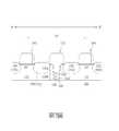
請參考第2(a)圖至第2(c)圖,其中,第2(a)圖為頂視圖,第2(b)圖為沿著第2(a)圖中A-A’切線的剖面示意圖,第2(c)圖為沿著第2(a)圖中B-B’切線的剖面示意圖。雖然A-A’切線為沿著鰭狀結構104延伸方向的剖面示意圖,但本領域技術人員應可理解,此一溝渠120係可同時延伸至鰭狀結構102、106,因此接下來的說明與附圖,同樣可用來說明鰭狀結構102、106沿其延伸方向的剖面結構。Please refer to Figures 2(a) to 2(c), where Figure 2(a) is the top view and Figure 2(b) is along the tangent line AA' in Figure 2(a) A schematic cross-sectional view. FIG. 2(c) is a schematic cross-sectional view taken along line BB′ in FIG. 2(a). Although the AA' tangent is a schematic cross-sectional view along the extending direction of the fin-shaped
首先,提供一基底100,例如矽基底、含矽基底,或矽覆絕緣(silicon-on-insulator,SOI)基底,並依序在基底100上形成氧化矽墊層132、氮化矽墊層134以及另一氧化矽墊層136。接著,於基底100中形成複數條互相平形的鰭狀結構102、104、106以及鰭間溝渠110,沿著鰭狀結構102、104、106的延伸方向包圍該鰭狀結構。如第2(a)圖和第2(c)圖所示,鰭狀結構104與相鄰的鰭狀結構102、106是由溝渠110隔離開。如第2(a)圖和第2(b)圖所示,溝渠120位於鰭狀結構102、104、106以及鰭間溝渠110中,並與鰭狀結構102、104、106的延伸方向垂直,分別將鰭狀結構102、104、106區分成至少兩個區段。First, provide a
可直接使用顯影暨蝕刻製程(PEP)等圖案化製程,以利用硬遮罩層作為蝕刻硬遮罩,蝕刻基底100形成鰭間溝渠110來定義出鰭狀結構102、104、106,或者,可進一步採用多重圖案化(multiple patterning)技術,包含間距微縮技術、側壁圖案轉移(sidewall image transfer,SIT)技術等,以完成更緊密排列的鰭狀結構圖案。為了簡化說明,上述圖案化過程在此並不贅述。接著,進行一鰭狀切割(fin cut)製程,例如單擴散隔離(single diffusion break,SDB)製程,於鰭狀結構102、104、106中形成溝渠120,分別將各鰭狀結構102、104、106隔離成至少兩個區段。鰭狀切割製程前,可包含先塗佈有機平坦層(organic planarization layer,OPL)或有機介電層(organic dielectric layer,ODL)於基底100上,填滿鰭間溝渠110並覆蓋鰭狀結構102、104、106,然後再進行另一次圖案化製程,於預定位置形成溝渠120。根據本發明一實施例,溝渠120的深度d2與鰭間溝渠110的深度d1與大致相同。根據本發明一實施例,溝渠120的寬度w2可小於或等於鰭間溝渠110的寬度w1。Patterning processes such as development and etching processes (PEP) can be used directly to use the hard mask layer as an etched hard mask, and the
第3圖至第5圖同樣為沿著第2(a)圖中A-A’切線的剖面示意圖,用來說明鰭狀結構104於後續各製作階段中,沿其延伸方向的剖面結構。FIGS. 3 to 5 are also schematic cross-sectional views along the tangent line A-A' in FIG. 2(a) to illustrate the cross-sectional structure of the fin-shaped
請參考第3圖。接著,可先選擇性形成一包含氧化矽或氮化矽的襯層(liner),再全面性地形成第一介電材料層140,例如氧化矽,覆蓋鰭狀結構104並填滿溝渠120。須注意的是,雖然第3圖並未繪示,但本領域技術人員應可理解,各鰭間溝渠110同時也被第一介電材料層140填滿。根據本發明一實施例,可利用流動式化學氣相沈積(flowable chemical vapor deposition,FCVD)製程形成第一介電材料層140,其具有優良的溝渠填充(gap filling)能力,可填充高深寬比(aspect ratio)的溝渠。後續,進行一退火製程142,使第一介電材料層140固化與致密化。根據所述實施例,退火製程142進行時,存在於第一介電材料層140中的氧,會進一步氧化與其接觸的基底100材料,形成一沿著溝渠120底部、側壁並延伸至頂角的氧化物層144。如第3圖所示,退火製程142後,溝渠120會具有圓化的頂角124以及向外(向基底)擴張的側壁122,並且具有包含氧化物層144厚度的寬度w2’以及深度d2’。Please refer to Figure 3. Then, a liner containing silicon oxide or silicon nitride can be selectively formed, and then a first
請參考第4圖。接著,利用化學機械研磨(chemical mechanical polishing,CMP)或回蝕刻製程,移除溝渠120外多餘的第一介電材料層140直到暴露出鰭狀結構104上的氧化矽墊層136,再依續移除氧化矽墊層136和氮化矽墊層134,剩下的氧化矽墊層132可用來當作一緩衝層,並使得溝渠120中的第一介電材料層140形成微高於鰭狀結構104上表面的第一介電層146。後續,進行離子植入製程150,將預定劑量及種類的摻雜植入鰭狀結構104中,形成井區152。根據本發明一實施例,溝渠120的深度d2’可大於或等於井區152的深度。Please refer to Figure 4. Next, using chemical mechanical polishing (CMP) or etch-back process, the redundant first
請參考第5圖。接著,進行一回蝕刻製程移除部分第一介電層146,使第一介電層146僅填充溝渠120的下部120b,暴露出溝渠120的上部120a。根據本發明一實施例,氧化矽墊層132以及位於頂角124和上部120a的上側壁126的氧化物層144,也會在回蝕刻製程中被移除,同時暴露出鰭狀結構104上表面、溝渠120頂角124和上側壁126。接著,利用例如原子層沉積法(ALD),形成一閘極介電層160,例如氧化矽,共形地覆蓋鰭狀結構104上表面、第一介電層146的上表面148,以及溝渠120的頂角124和上側壁126。根據所述實施例,利用原子層沉積法形成閘極介電層160,可避免位於溝渠120的頂角124和上側壁126的基底100被氧化而耗損。Please refer to Figure 5. Next, an etching process is performed to remove part of the
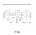
請參考第6(a)圖和第6(b)圖。第6(a)圖為頂視圖,第6(b)圖為沿著第6(a)圖中A-A’切線的剖面示意圖。在形成閘極介電層160之後,接著,形成閘極結構170和180,跨越鰭狀結構102、104、106並與鰭狀結構102、104、106的長度延伸方向垂直,其中,閘極結構170包含閘極體172及側壁子174,位於溝渠120上並完全覆蓋溝渠120。閘極結構180包含閘極體182及側壁子184,各分別位於溝渠120兩側的鰭狀結構104上。根據本發明一實施例,形成閘極結構170、180的步驟包含沉積一閘極體材料層,例如多晶矽(poly silicon)或非晶相矽(amorphous silicon),全面性地覆蓋鰭狀結構102、104、106,然後進行平坦化及圖案化步驟形成閘極體172、182,再於閘極體172、182的相對側壁上形成側壁子174、184,例如氧化矽或氮化矽側壁子。如第6(b)圖所示,閘極體172對準並完全覆蓋溝渠120,並且填入溝渠120的上部120a。換句話說,溝渠120兩側的鰭狀結構104的端點,均被閘極體172覆蓋,並未暴露出來。閘極介電層160位於閘極體172、第一介電層146的上表面148、溝渠120的頂角124以及上側壁126之間,而約略具有一倒Ω形狀。根據本發明一實施例,閘極體172的寬度w3可大於或等於溝渠120的寬度w2’。根據本發明一實施例,閘極體172具有一低於鰭狀結構104的上表面50至100埃(Å)的底面,其中,覆蓋溝渠120上側壁126的閘極介電層會位於於覆蓋下側壁128的氧化物層144之上,並且切齊氧化物層144。Please refer to Figure 6(a) and Figure 6(b). Figure 6(a) is a top view, and Figure 6(b) is a schematic cross-sectional view taken along the line A-A' in Figure 6(a). After the
第7圖至第11圖同樣為沿著第6(a)圖中A-A’切線的剖面示意圖,用來說明鰭狀結構104於後續各製作階段中,沿其延伸方向的剖面結構。FIGS. 7 to 11 are also schematic cross-sectional views along the tangent line A-A' in FIG. 6(a) to illustrate the cross-sectional structure of the fin-shaped
請參考第7圖。接著,在閘極結構170和180兩側的鰭狀結構104中形成磊晶層190,後續作為元件的源/汲極區192。可利用閘極結構170和180作為自對準結構,於其兩側的鰭狀結構104中蝕刻出凹槽,然後利用磊晶成長製程於凹槽中形成磊晶層190。可在磊晶成長時就加入摻雜(doping),或磊晶成長後再植入摻雜,使得磊晶層190具有適當的摻雜種類及濃度,作為元件的源/汲極區192。根據本發明一實施例,源/汲極區192鄰近溝渠120的上側壁126但不直接接觸。源/汲極區192具有低於該第一介電層146的上表面148的底面。如第7圖所示的實施例,在進行磊晶成長前,藉由重新形成的氧化物介電層160,和形成閘極體172完全覆蓋並填滿溝渠120的上部120a,可有效避免磊晶成長時,溝渠120兩側的磊晶層190發生橋接。另外,也藉由以閘極結構170作為自對準結構於鰭狀結構104中形成凹槽,使得凹槽可與溝渠120的側壁122保持一定距離,溝渠120的側壁122並不會自凹槽暴露出來而對磊晶成長造成影響,產生晶面缺陷。值得注意的是,本發明以單一閘極結構170完全覆蓋溝渠120,可使其兩側的閘極結構180之間具有較緊密的間距P1,實現較小的佈局面積。Please refer to Figure 7. Next, an
請參考第8圖。接著,於基底100上形成接觸蝕刻停止層210以及層間介電層220,全面性地覆蓋源/汲極區192以及閘極結構170、180,然後進行平坦化步驟,移除部分的接觸蝕刻停止層210與層間介電層220,曝露出閘極結構170、180的頂面。Please refer to Figure 8. Next, a contact
第9圖至第10圖說明後續進行一取代金屬閘極製程(replacement metal gate,RMG),製作金屬閘極結構。9 to 10 illustrate a subsequent replacement metal gate (RMG) process to fabricate a metal gate structure.
請參考第9圖。自閘極結構170、180的頂面移除閘極體172、182,形成閘極溝渠176、186,暴露出部分閘極介電層160。接著,可利用例如化學氧化物移除(chemical oxide removal,COR)製程移除暴露的閘極介電層160。值得注意的是,進行化學氧化物移除製程時,部分溝渠120的頂角124、上側壁126,以及第一介電層146的上表面148也會受到蝕刻,而變成圓化的頂角124’、凹面的上側壁126’和凹面的上表面148’,自閘極溝渠176暴露出來。根據本發明一實施例,源/汲極區192與上側壁126’之間仍保有一間距,並不直接接觸,並且源/汲極區192的底面仍低於該第一介電層146的上表面148’。根據本發明一實施例,側壁子174與鰭狀結構104之間的閘極介電層160,其暴露於閘極溝渠176底部的端點也會受到部份蝕刻而往後退縮,因此形成底切(undercut)162,其位於側壁子174的內側壁(閘極溝渠176的側壁)底部。Please refer to Figure 9. The
請參考第10圖。接著,可利用熱氧化製程,於鰭狀結構104、頂角124’和上側壁126’形成一介面層310,例如氧化矽。然後,再形成一高介電常數介電層320,共形地覆蓋介面層310、第一介電層146的上表面148’,和閘極溝渠176、186的側壁。後續,再形成一金屬閘極體330,填充閘極溝渠176、186以及溝渠120的上部120a,完成金屬閘極結構178、188。填充於閘極溝渠176以及上部120a的金屬閘極體330,具有一低於鰭狀結構104上表面50至100埃(Å)的底面。在本發明一實施例中,金屬閘極結構178可以是不與外部電連接的虛置閘極(dummy gate),或是連接到其他鰭式場效電晶體的閘極,又或是與外部電連接的區域內連線(local inter-connect)結構。金屬閘極結構178與鰭狀結構104中的第一介電層146、介面層310以及高介電常數介電層320形成一單擴散隔離結構(single diffusion break isolation)。Please refer to Figure 10. Then, a thermal oxidation process may be used to form an
如第10圖所示的實施例,本發明提供的半導體結構,包含一位於鰭狀結構104中的溝渠120,以及一對準於溝渠的金屬閘極結構178,位於溝渠120上。溝渠120的上部120a由金屬閘極體330填充,並且具有凹面的上側壁126’。溝渠120的下部120b由第一介電層146填充,並且具有的筆直的下側壁128。溝渠120還具有圓化的頂角124’,與凹面的上側壁126’以及筆直的下側壁128共同構成本發明特徵之一的溝渠120側壁122’。介面層310以及高介電常數介電層320覆蓋溝渠120的頂角124’和上側壁126’,並介於金屬閘極體330、第一介電層146的凹面上表面148’、溝渠120的頂角124’和上側壁126’之間,其中,高介電常數介電層320往上延伸至金屬閘極體330與側壁子174之間。值得注意的是,介面層310及/或高介電常數介電層320,會沿著閘極介電層160的底切162延伸至側壁子174底部,使得介面層310及/或高介電常數介電層320在接近頂角124’以及側壁子174的內側壁底部的部分會具有一喙狀輪廓。As shown in the embodiment shown in FIG. 10, the semiconductor structure provided by the present invention includes a
請參考第11圖。後續,再形成另一層間介電層230,覆蓋於層間介電層220以及金屬閘極結構178、188,並形成複數個接觸插塞410、420,分別與源/汲極區192和金屬閘極結構188電連接。Please refer to Figure 11. Subsequently, another
本發明提供的隔離結構及其製作方法,可將連續的鰭狀結構區分成數個區段,後續再根據布局設計,製作成個別的鰭狀場效電晶體。該隔離結構不僅具有較小的寬度,可實現較緊密的布局,還可避免鰭狀結構端點的磊晶橋接缺陷,同時也可避免磊晶成長時產生晶面缺陷,改善接觸插塞的良率。The isolation structure and the manufacturing method provided by the present invention can divide the continuous fin structure into several sections, and then make individual fin field effect transistors according to the layout design. The isolation structure not only has a smaller width, can achieve a tighter layout, but also can avoid epitaxial bridging defects at the ends of the fin structure, and can also avoid crystal surface defects during epitaxial growth, improving the goodness of contact plugs. rate.
以上所述僅為本發明之較佳實施例,凡依本發明申請專利範圍所做之均等變化與修飾,皆應屬本發明之涵蓋範圍。The above are only the preferred embodiments of the present invention, and all changes and modifications made in accordance with the scope of the patent application of the present invention shall fall within the scope of the present invention.
100:基底100: base
120a:上部120a: upper part
120b:下部120b: Lower
122':側壁122': sidewall
124':頂角124': top corner
126':上側壁126': upper side wall
128:下側壁128: lower side wall
146:第一介電層146: first dielectric layer
148':上表面148': upper surface
152:井區152: Well District
174、184:側壁子174, 184: side wall
178、188:金屬閘極結構178, 188: metal gate structure
190:磊晶層190: Epitaxial layer
192:源/汲極區192: source/drain region
210:接觸蝕刻停止層210: Contact etching stop layer
220:層間介電層220: interlayer dielectric layer
310:介面層310: interface layer
320:高介電常數介電層320: High dielectric constant dielectric layer
330:金屬閘極體330: Metal gate body
Claims (21)
Translated fromChinesePriority Applications (3)
| Application Number | Priority Date | Filing Date | Title |
|---|---|---|---|
| TW105124552ATWI691076B (en) | 2016-08-03 | 2016-08-03 | Semiconductor structure and method of forming the same |
| US15/249,462US10043868B2 (en) | 2016-08-03 | 2016-08-28 | Semiconductor structure and method of forming the same |
| US16/028,386US10658458B2 (en) | 2016-08-03 | 2018-07-05 | Semiconductor structure and method of forming the same |
Applications Claiming Priority (1)
| Application Number | Priority Date | Filing Date | Title |
|---|---|---|---|
| TW105124552ATWI691076B (en) | 2016-08-03 | 2016-08-03 | Semiconductor structure and method of forming the same |
Publications (2)
| Publication Number | Publication Date |
|---|---|
| TW201806156A TW201806156A (en) | 2018-02-16 |
| TWI691076Btrue TWI691076B (en) | 2020-04-11 |
Family
ID=61069795
Family Applications (1)
| Application Number | Title | Priority Date | Filing Date |
|---|---|---|---|
| TW105124552ATWI691076B (en) | 2016-08-03 | 2016-08-03 | Semiconductor structure and method of forming the same |
Country Status (2)
| Country | Link |
|---|---|
| US (2) | US10043868B2 (en) |
| TW (1) | TWI691076B (en) |
Families Citing this family (14)
| Publication number | Priority date | Publication date | Assignee | Title |
|---|---|---|---|---|
| KR102524806B1 (en) | 2016-08-11 | 2023-04-25 | 삼성전자주식회사 | Semiconductor device including a contact structure |
| CN109216191B (en)* | 2017-06-29 | 2022-08-16 | 蓝枪半导体有限责任公司 | Semiconductor element and manufacturing method thereof |
| US10439026B2 (en)* | 2017-10-17 | 2019-10-08 | Globalfoundries Inc. | Fins with single diffusion break facet improvement using epitaxial insulator |
| US10777466B2 (en)* | 2017-11-28 | 2020-09-15 | Taiwan Semiconductor Manufacturing Co., Ltd. | Semiconductor Fin cutting process and structures formed thereby |
| US10916478B2 (en)* | 2018-02-20 | 2021-02-09 | Globalfoundries U.S. Inc. | Methods of performing fin cut etch processes for FinFET semiconductor devices |
| CN110581128B (en) | 2018-06-07 | 2022-05-10 | 联华电子股份有限公司 | Semiconductor structure and method of making the same |
| US10475693B1 (en)* | 2018-06-07 | 2019-11-12 | Globalfoundries Inc. | Method for forming single diffusion breaks between finFET devices and the resulting devices |
| DE102019121750B4 (en)* | 2018-08-31 | 2023-09-21 | Taiwan Semiconductor Manufacturing Co., Ltd. | METAL GATE STRUCTURE CUTTING METHOD AND SEMICONDUCTOR DEVICE PRODUCED THEREFROM |
| US10930564B2 (en) | 2018-08-31 | 2021-02-23 | Taiwan Semiconductor Manufacturing Co., Ltd. | Metal gate structure cutting process |
| KR102492304B1 (en) | 2018-10-01 | 2023-01-27 | 삼성전자주식회사 | Semiconductor device |
| US11164866B2 (en)* | 2019-02-20 | 2021-11-02 | Taiwan Semiconductor Manufacturing Co., Ltd. | Semiconductor structure and method for manufacturing the same |
| US11004751B2 (en)* | 2019-02-25 | 2021-05-11 | International Business Machines Corporation | Vertical transistor having reduced edge fin variation |
| CN112017960B (en)* | 2019-05-28 | 2024-09-20 | 中芯国际集成电路制造(上海)有限公司 | Semiconductor structure and forming method thereof |
| US11640990B2 (en)* | 2020-10-27 | 2023-05-02 | Wolfspeed, Inc. | Power semiconductor devices including a trenched gate and methods of forming such devices |
Citations (5)
| Publication number | Priority date | Publication date | Assignee | Title |
|---|---|---|---|---|
| US20050054204A1 (en)* | 2003-09-04 | 2005-03-10 | Chien-An Yu | Method of rounding top corner of trench |
| US20140035066A1 (en)* | 2012-07-31 | 2014-02-06 | Shih-Hung Tsai | Non-Planar FET and Manufacturing Method Thereof |
| TW201442147A (en)* | 2013-04-17 | 2014-11-01 | United Microelectronics Corp | Method of forming an isolation structure |
| TW201612972A (en)* | 2014-09-30 | 2016-04-01 | Taiwan Semiconductor Mfg Co Ltd | Dry etching apparatus and method of manufacturing Fin-FET devices |
| TW201626571A (en)* | 2014-10-17 | 2016-07-16 | 台灣積體電路製造股份有限公司 | Fin field effect transistor device structure and forming method thereof |
Family Cites Families (7)
| Publication number | Priority date | Publication date | Assignee | Title |
|---|---|---|---|---|
| KR100724561B1 (en)* | 2005-12-20 | 2007-06-04 | 삼성전자주식회사 | Semiconductor device with single sidewall fin field effect transistor and its formation method |
| US9324866B2 (en) | 2012-01-23 | 2016-04-26 | Taiwan Semiconductor Manufacturing Company, Ltd. | Structure and method for transistor with line end extension |
| US9041099B2 (en)* | 2011-04-11 | 2015-05-26 | Nanya Technology Corp. | Single-sided access device and fabrication method thereof |
| CN102646599B (en) | 2012-04-09 | 2014-11-26 | 北京大学 | Preparation method of FinFET (Fin Field Effect Transistor) in large-scale integration circuit |
| US9006094B2 (en)* | 2012-04-18 | 2015-04-14 | International Business Machines Corporation | Stratified gate dielectric stack for gate dielectric leakage reduction |
| US9082853B2 (en)* | 2012-10-31 | 2015-07-14 | International Business Machines Corporation | Bulk finFET with punchthrough stopper region and method of fabrication |
| US9515172B2 (en)* | 2014-01-28 | 2016-12-06 | Samsung Electronics Co., Ltd. | Semiconductor devices having isolation insulating layers and methods of manufacturing the same |
- 2016
- 2016-08-03TWTW105124552Apatent/TWI691076B/enactive
- 2016-08-28USUS15/249,462patent/US10043868B2/enactiveActive
- 2018
- 2018-07-05USUS16/028,386patent/US10658458B2/enactiveActive
Patent Citations (5)
| Publication number | Priority date | Publication date | Assignee | Title |
|---|---|---|---|---|
| US20050054204A1 (en)* | 2003-09-04 | 2005-03-10 | Chien-An Yu | Method of rounding top corner of trench |
| US20140035066A1 (en)* | 2012-07-31 | 2014-02-06 | Shih-Hung Tsai | Non-Planar FET and Manufacturing Method Thereof |
| TW201442147A (en)* | 2013-04-17 | 2014-11-01 | United Microelectronics Corp | Method of forming an isolation structure |
| TW201612972A (en)* | 2014-09-30 | 2016-04-01 | Taiwan Semiconductor Mfg Co Ltd | Dry etching apparatus and method of manufacturing Fin-FET devices |
| TW201626571A (en)* | 2014-10-17 | 2016-07-16 | 台灣積體電路製造股份有限公司 | Fin field effect transistor device structure and forming method thereof |
Also Published As
| Publication number | Publication date |
|---|---|
| US20180040694A1 (en) | 2018-02-08 |
| US10658458B2 (en) | 2020-05-19 |
| TW201806156A (en) | 2018-02-16 |
| US20180331177A1 (en) | 2018-11-15 |
| US10043868B2 (en) | 2018-08-07 |
Similar Documents
| Publication | Publication Date | Title |
|---|---|---|
| TWI691076B (en) | Semiconductor structure and method of forming the same | |
| TWI692871B (en) | Semiconductor structure and its manufacturing method | |
| CN108122768B (en) | Method for forming semiconductor device | |
| KR100764745B1 (en) | Semiconductor device having semi-cylindrical active region and manufacturing method thereof | |
| TWI509736B (en) | Semiconductor structure and method of forming same | |
| TWI598946B (en) | Semiconductor device and method of manufacturing same | |
| JP4667736B2 (en) | Method for manufacturing MOS transistor with multiple channels | |
| TW202013604A (en) | Method for forming semiconductor device | |
| US11742414B2 (en) | Semiconductor device with fins | |
| US8378395B2 (en) | Methods of fabricating field effect transistors having protruded active regions | |
| US11075121B2 (en) | Semiconductor devices and fabrication methods thereof | |
| CN108630544B (en) | Semiconductor element and manufacturing method thereof | |
| TWI728966B (en) | Semiconductor device and method for fabricating the same | |
| TWI703732B (en) | Method for fabricating semiconductor device | |
| CN108074974B (en) | Method of forming semiconductor device | |
| CN111009529B (en) | Non-volatile memory structure and manufacturing method thereof | |
| CN109300971B (en) | Semiconductor structure and method of making the same | |
| KR100912960B1 (en) | Transistor having recess channel and manufacturing method thereof | |
| KR100611083B1 (en) | MOS transistor and its manufacturing method | |
| KR20090002655A (en) | Semiconductor device manufacturing method | |
| KR100732269B1 (en) | Semiconductor element and manufacturing method thereof | |
| CN111613532B (en) | Forming method of field effect transistor and field effect transistor | |
| TW202515334A (en) | Semiconductor device | |
| TW202301682A (en) | Semiconductor device | |
| KR20040046074A (en) | Method for forming Field effect transistors of semiconductor device |