TWI690933B - Variable resistance random-access memory - Google Patents
Variable resistance random-access memoryDownload PDFInfo
- Publication number
- TWI690933B TWI690933BTW108116499ATW108116499ATWI690933BTW I690933 BTWI690933 BTW I690933BTW 108116499 ATW108116499 ATW 108116499ATW 108116499 ATW108116499 ATW 108116499ATW I690933 BTWI690933 BTW I690933B
- Authority
- TW
- Taiwan
- Prior art keywords
- data
- variable resistance
- memory unit
- memory
- random access
- Prior art date
Links
Images


Classifications
- G—PHYSICS
- G11—INFORMATION STORAGE
- G11C—STATIC STORES
- G11C13/00—Digital stores characterised by the use of storage elements not covered by groups G11C11/00, G11C23/00, or G11C25/00
- G11C13/0002—Digital stores characterised by the use of storage elements not covered by groups G11C11/00, G11C23/00, or G11C25/00 using resistive RAM [RRAM] elements
- G11C13/0021—Auxiliary circuits
- G11C13/0023—Address circuits or decoders
- G11C13/0026—Bit-line or column circuits
- G—PHYSICS
- G11—INFORMATION STORAGE
- G11C—STATIC STORES
- G11C29/00—Checking stores for correct operation ; Subsequent repair; Testing stores during standby or offline operation
- G11C29/04—Detection or location of defective memory elements, e.g. cell constructio details, timing of test signals
- G11C29/08—Functional testing, e.g. testing during refresh, power-on self testing [POST] or distributed testing
- G11C29/12—Built-in arrangements for testing, e.g. built-in self testing [BIST] or interconnection details
- G11C29/38—Response verification devices
- G11C29/42—Response verification devices using error correcting codes [ECC] or parity check
- G—PHYSICS
- G06—COMPUTING OR CALCULATING; COUNTING
- G06F—ELECTRIC DIGITAL DATA PROCESSING
- G06F11/00—Error detection; Error correction; Monitoring
- G06F11/07—Responding to the occurrence of a fault, e.g. fault tolerance
- G06F11/08—Error detection or correction by redundancy in data representation, e.g. by using checking codes
- G06F11/10—Adding special bits or symbols to the coded information, e.g. parity check, casting out 9's or 11's
- G06F11/1008—Adding special bits or symbols to the coded information, e.g. parity check, casting out 9's or 11's in individual solid state devices
- G06F11/1012—Adding special bits or symbols to the coded information, e.g. parity check, casting out 9's or 11's in individual solid state devices using codes or arrangements adapted for a specific type of error
- G—PHYSICS
- G06—COMPUTING OR CALCULATING; COUNTING
- G06F—ELECTRIC DIGITAL DATA PROCESSING
- G06F11/00—Error detection; Error correction; Monitoring
- G06F11/07—Responding to the occurrence of a fault, e.g. fault tolerance
- G06F11/08—Error detection or correction by redundancy in data representation, e.g. by using checking codes
- G06F11/10—Adding special bits or symbols to the coded information, e.g. parity check, casting out 9's or 11's
- G06F11/1008—Adding special bits or symbols to the coded information, e.g. parity check, casting out 9's or 11's in individual solid state devices
- G06F11/1048—Adding special bits or symbols to the coded information, e.g. parity check, casting out 9's or 11's in individual solid state devices using arrangements adapted for a specific error detection or correction feature
- G—PHYSICS
- G11—INFORMATION STORAGE
- G11C—STATIC STORES
- G11C13/00—Digital stores characterised by the use of storage elements not covered by groups G11C11/00, G11C23/00, or G11C25/00
- G11C13/0002—Digital stores characterised by the use of storage elements not covered by groups G11C11/00, G11C23/00, or G11C25/00 using resistive RAM [RRAM] elements
- G11C13/0021—Auxiliary circuits
- G11C13/0023—Address circuits or decoders
- G11C13/0028—Word-line or row circuits
- G—PHYSICS
- G11—INFORMATION STORAGE
- G11C—STATIC STORES
- G11C13/00—Digital stores characterised by the use of storage elements not covered by groups G11C11/00, G11C23/00, or G11C25/00
- G11C13/0002—Digital stores characterised by the use of storage elements not covered by groups G11C11/00, G11C23/00, or G11C25/00 using resistive RAM [RRAM] elements
- G11C13/0021—Auxiliary circuits
- G11C13/0033—Disturbance prevention or evaluation; Refreshing of disturbed memory data
- G—PHYSICS
- G11—INFORMATION STORAGE
- G11C—STATIC STORES
- G11C13/00—Digital stores characterised by the use of storage elements not covered by groups G11C11/00, G11C23/00, or G11C25/00
- G11C13/0002—Digital stores characterised by the use of storage elements not covered by groups G11C11/00, G11C23/00, or G11C25/00 using resistive RAM [RRAM] elements
- G11C13/0021—Auxiliary circuits
- G11C13/0035—Evaluating degradation, retention or wearout, e.g. by counting writing cycles
- G—PHYSICS
- G11—INFORMATION STORAGE
- G11C—STATIC STORES
- G11C13/00—Digital stores characterised by the use of storage elements not covered by groups G11C11/00, G11C23/00, or G11C25/00
- G11C13/0002—Digital stores characterised by the use of storage elements not covered by groups G11C11/00, G11C23/00, or G11C25/00 using resistive RAM [RRAM] elements
- G11C13/0021—Auxiliary circuits
- G11C13/004—Reading or sensing circuits or methods
- G—PHYSICS
- G11—INFORMATION STORAGE
- G11C—STATIC STORES
- G11C13/00—Digital stores characterised by the use of storage elements not covered by groups G11C11/00, G11C23/00, or G11C25/00
- G11C13/0002—Digital stores characterised by the use of storage elements not covered by groups G11C11/00, G11C23/00, or G11C25/00 using resistive RAM [RRAM] elements
- G11C13/0021—Auxiliary circuits
- G11C13/0064—Verifying circuits or methods
- G—PHYSICS
- G11—INFORMATION STORAGE
- G11C—STATIC STORES
- G11C13/00—Digital stores characterised by the use of storage elements not covered by groups G11C11/00, G11C23/00, or G11C25/00
- G11C13/0002—Digital stores characterised by the use of storage elements not covered by groups G11C11/00, G11C23/00, or G11C25/00 using resistive RAM [RRAM] elements
- G11C13/0021—Auxiliary circuits
- G11C13/0069—Writing or programming circuits or methods
- G—PHYSICS
- G11—INFORMATION STORAGE
- G11C—STATIC STORES
- G11C29/00—Checking stores for correct operation ; Subsequent repair; Testing stores during standby or offline operation
- G11C29/52—Protection of memory contents; Detection of errors in memory contents
- G—PHYSICS
- G11—INFORMATION STORAGE
- G11C—STATIC STORES
- G11C13/00—Digital stores characterised by the use of storage elements not covered by groups G11C11/00, G11C23/00, or G11C25/00
- G11C13/0002—Digital stores characterised by the use of storage elements not covered by groups G11C11/00, G11C23/00, or G11C25/00 using resistive RAM [RRAM] elements
- G11C13/0021—Auxiliary circuits
- G11C13/0064—Verifying circuits or methods
- G11C2013/0066—Verify correct writing whilst writing is in progress, e.g. by detecting onset or cessation of current flow in cell and using the detector output to terminate writing
- G—PHYSICS
- G11—INFORMATION STORAGE
- G11C—STATIC STORES
- G11C13/00—Digital stores characterised by the use of storage elements not covered by groups G11C11/00, G11C23/00, or G11C25/00
- G11C13/0002—Digital stores characterised by the use of storage elements not covered by groups G11C11/00, G11C23/00, or G11C25/00 using resistive RAM [RRAM] elements
- G11C13/0021—Auxiliary circuits
- G11C13/0069—Writing or programming circuits or methods
- G11C2013/0073—Write using bi-directional cell biasing
- G—PHYSICS
- G11—INFORMATION STORAGE
- G11C—STATIC STORES
- G11C29/00—Checking stores for correct operation ; Subsequent repair; Testing stores during standby or offline operation
- G11C29/04—Detection or location of defective memory elements, e.g. cell constructio details, timing of test signals
- G11C2029/0411—Online error correction
- G—PHYSICS
- G11—INFORMATION STORAGE
- G11C—STATIC STORES
- G11C2213/00—Indexing scheme relating to G11C13/00 for features not covered by this group
- G11C2213/70—Resistive array aspects
- G11C2213/79—Array wherein the access device being a transistor
- G—PHYSICS
- G11—INFORMATION STORAGE
- G11C—STATIC STORES
- G11C2213/00—Indexing scheme relating to G11C13/00 for features not covered by this group
- G11C2213/70—Resistive array aspects
- G11C2213/82—Array having, for accessing a cell, a word line, a bit line and a plate or source line receiving different potentials
Landscapes
- Engineering & Computer Science (AREA)
- Theoretical Computer Science (AREA)
- Quality & Reliability (AREA)
- Physics & Mathematics (AREA)
- General Engineering & Computer Science (AREA)
- General Physics & Mathematics (AREA)
- For Increasing The Reliability Of Semiconductor Memories (AREA)
Abstract
Description
Translated fromChinese本發明是有關於一種半導體記憶體裝置,更具體來說是一種使用可變電阻元件的可變電阻隨機存取記憶體(variable resistance random-access memory,RRAM)。The present invention relates to a semiconductor memory device, and more particularly to a variable resistance random-access memory (RRAM) using variable resistance elements.
可變電阻記憶體藉由施加脈衝電壓至可變電阻元件並且設定可變電阻元件以可逆及非揮發性的方式至高阻抗狀態或低阻抗狀態來儲存資料。可變電阻記憶體的優點是於低電壓時重寫資料,所以功率消耗低且讀取時間短(專利文件1:日本特開2012-64286號公報、專利文件2:日本特開2008-41704號公報等)。The variable resistance memory stores data by applying a pulse voltage to the variable resistance element and setting the variable resistance element to a high impedance state or a low impedance state in a reversible and non-volatile manner. The advantage of the variable resistance memory is that the data is rewritten at low voltage, so the power consumption is low and the reading time is short (Patent Document 1: Japanese Patent Publication No. 2012-64286, Patent Document 2: Japanese Patent Publication No. 2008-41704 Bulletin, etc.).
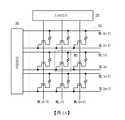
圖1A繪示3行×3列的記憶體陣列10。每一個記憶單元MC是所謂的1T×1R,其包括由一個可變電阻元件以及一個與可變電阻元件串接的電晶體。可變電阻元件包括像是氧化鉿(hafnium oxide,HfOx)的過渡金屬氧化物的薄膜,藉由改變寫入脈衝電壓的極性或數值來將其設定至低阻抗狀態或高阻抗狀態。一般來說,將可變電阻元件寫入至低阻抗狀態稱作設置(後稱SET),寫入至高阻抗狀態稱作重置(後稱RESET)。FIG. 1A shows a
圖1B繪示於形成、設置與重置期間時所選用的偏壓的例子。於存取記憶單元MC時,透過行解碼器20經由字元線WL(n)將記憶單元MC的電晶體開啟,並透過列解碼器30經由位元線BL(n)與源極線SL(n)施加相應於SET或RESET的脈衝電壓。於讀取操作時,經由感測電路感測通過記憶單元MC的電壓或電流,並據此判斷其中的可變電阻元件為低阻抗狀態或高阻抗狀態。FIG. 1B illustrates an example of the bias voltages selected during the formation, setup, and reset periods. When accessing the memory cell MC, the transistor of the memory cell MC is turned on through the word line WL(n) through the
此外,形成是指施加比設置時所施加的電壓還高的電壓,以初始設定可變電阻元件為低阻抗狀態。In addition, forming means applying a voltage higher than the voltage applied during installation, and initially setting the variable resistance element to a low impedance state.
圖2繪示一般的可變電阻記憶體的示意架構的方塊圖。可變電阻記憶體包括控制器50、主記憶體部60、子記憶體部70,以及ECC(error checking and correcting)電路80等。控制器50從外部接收指令、位址等,以控制讀取操作和寫入操作(SET/RESET)。主記憶體部60和子記憶體部70均具有包括可變電阻元件的多個記憶體陣列,主記憶體部60儲存於寫入操作期間來自外部的資料,子記憶體部70儲存由ECC電路80產生的碼資訊,即,用以錯誤偵測/校正的錯誤校正碼。FIG. 2 is a block diagram showing a schematic structure of a general variable resistance memory. The variable resistance memory includes a
當寫入輸入資料至主記憶體部60,ECC電路80對輸入資料執行ECC操作並產生錯誤校正碼。當寫入輸入資料時,寫入與輸入資料相關的錯誤校正碼至子記憶體部70。再者,當從主記憶體部60讀取資料時,從子記憶體部70讀取錯誤校正碼,ECC電路80對從主記憶體部60讀取與錯誤校正碼相關的資料執行錯誤檢查校正,且輸出結果到外部作為讀取資料。When writing input data to the
在可變電阻記憶體中,已知當SET/RESET寫入次數(循環次數)增加,可變電阻元件的狀態變成不穩定。換句話說,即使執行SET寫入,可變電阻元件也不能改變成低阻抗,即使執行RESET寫入,可變電阻元件也不能改變成高阻抗。當錯誤位元出現時,ECC電路80可保證準確的資料。In the variable resistance memory, it is known that when the number of SET/RESET writes (cycle number) increases, the state of the variable resistance element becomes unstable. In other words, even if SET writing is performed, the variable resistance element cannot be changed to low impedance, and even if RESET writing is performed, the variable resistance element cannot be changed to high impedance. When an error bit occurs, the
假如ECC電路80的處理能力增加,即,如果可校正的位元數量增加,則相對地可修復大量的錯誤位元。然而,隨著ECC電路80可校正的位元數量增加,ECC電路80所佔的面積增加,且可變電阻記憶體的效能會取決於ECC電路80的操作時間等的影響。因此,期望ECC電路80校正的位元數量要盡可能的少,且最終不必裝設ECC電路80。If the processing capacity of the
鑒於上述情況,本發明提供可變電阻隨機存取記憶體,其在修復失效記憶單元的同時抑制性能下降。In view of the above-mentioned circumstances, the present invention provides a variable resistance random access memory, which suppresses performance degradation while repairing a failed memory cell.
本發明的一實施例敘述可變電阻隨機存取記憶體。可變電阻隨機存取記憶體包括記憶體陣列、寫入部、判定部、保存部以及修復部。記憶體陣列包括多個記憶單元。寫入部將資料寫入到基於位址資訊而選擇的記憶單元。判定部判定寫入至所選擇的記憶單元的資料為有效或失效。保存部保存失效資訊,失效資訊包括判定為失效記憶單元的位址。當預定事件發生時,修復部基於失效資訊而重寫記憶單元的資料。An embodiment of the invention describes a variable resistance random access memory. The variable resistance random access memory includes a memory array, a writing part, a judging part, a saving part, and a repairing part. The memory array includes multiple memory cells. The writing part writes the data to the memory unit selected based on the address information. The determination unit determines whether the data written to the selected memory unit is valid or invalid. The storage unit stores the failure information, and the failure information includes the address of the memory unit determined to be failure. When the scheduled event occurs, repair the baseRewrite the data of the memory unit based on the failure information.
根據本發明,由於當預定事件發生時判定為失效的記憶單元的資料被重寫,修復判定為失效的記憶單元是有可能的。藉著修復判定為失效的記憶單元,錯誤校正電路校正的位元數量可被降低,且由於錯誤校正電路所造成的可變電阻隨機存取記憶體性能惡化可被抑制。According to the present invention, since the data of the memory unit determined to be failed when a predetermined event occurs is rewritten, it is possible to repair the memory unit determined to be failed. By repairing memory cells determined to be defective, the number of bits corrected by the error correction circuit can be reduced, and the performance deterioration of the variable resistance random access memory caused by the error correction circuit can be suppressed.
10:記憶體陣列10: memory array
100:可變電阻隨機存取記憶體100: variable resistance random access memory
110:記憶體陣列110: memory array
110A:主記憶體部110A: Main memory
110B:子記憶體部110B: Sub memory section
120:行選擇電路120: Row selection circuit
130:列選擇電路130: Column selection circuit
140:控制器140: controller
150:ECC電路150: ECC circuit
160:錯誤位元旗標暫存器160: Error bit flag register
170:錯誤位元位址暫存器170: Error bit address register
20:行解碼器20: Line decoder
30:列解碼器30: Column decoder
50:控制器50: controller
60:主記憶體部60: Main memory
70:子記憶體部70: Sub-memory department
80:ECC電路80: ECC circuit
MC:記憶單元MC: Memory unit
BL(n)、BL(n-1)、BL(n+1):位元線BL(n), BL(n-1), BL(n+1): bit line
SL(n)、SL(n-1)、SL(n+1):源極線SL(n), SL(n-1), SL(n+1): source line
WL(n)、WL(n-1)、WL(n+1):字元線WL(n), WL(n-1), WL(n+1): word line
S100、S110、S120、S130、S200、S210、S220、S230、S240、S250、S260、S300、S310、S320、S330、S340、S350、S360、S370:步驟S100, S110, S120, S130, S200, S210, S220, S230, S240, S250, S260, S300, S310, S320, S330, S340, S350, S360, S370: steps
圖1A 是說明傳統可變電阻隨機存取記憶體的陣列結構的圖。FIG. 1A is a diagram illustrating an array structure of a conventional variable resistance random access memory.
圖1B 是說明於各操作期間所選用的偏壓條件的表。FIG. 1B is a table illustrating the bias conditions selected during each operation.
圖2 是說明傳統可變電阻隨機存取記憶體的示意架構的方塊圖。FIG. 2 is a block diagram illustrating a schematic structure of a conventional variable resistance random access memory.
圖3 是根據本發明一實施例說明可變電阻隨機存取記憶體的示意架構的方塊圖。3 is a block diagram illustrating a schematic architecture of a variable resistance random access memory according to an embodiment of the invention.
圖4 是根據本發明一實施例說明指令處理序列範例的圖。4 is a diagram illustrating an example of an instruction processing sequence according to an embodiment of the invention.
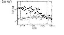
圖5A和圖5B 是說明可變電阻記憶體的阻抗狀態以及寫入周期數之間關係的圖。5A and 5B are diagrams illustrating the relationship between the resistance state of the variable resistance memory and the number of write cycles.
圖6 是根據本發明一實施例說明具有錯誤位元修復功能的寫入操作的流程圖。6 is a flowchart illustrating a write operation with an error bit repair function according to an embodiment of the invention.
圖7 是說明錯誤位元旗標暫存器的儲存範例的圖。FIG. 7 is a diagram illustrating a storage example of the error bit flag register.
圖8 是說明錯誤位元位址暫存器的儲存範例的圖。FIG. 8 is a diagram illustrating a storage example of the error bit address register.
圖9 是根據本發明一實施例說明錯誤位元的重寫操作的流程圖。FIG. 9 is a flowchart illustrating an error bit rewriting operation according to an embodiment of the present invention.
本發明例示的可變電阻隨機存取記憶體(以下簡稱RRAM)可由一個晶片組成,或是可嵌入於一個晶片中。圖3是根據本發明一實施例說明RRAM的示意架構的方塊圖。本實施例中的RRAM 100包括記憶體陣列110、行選擇電路120、列選擇電路130、控制器140、ECC電路150、錯誤位元旗標暫存器160以及錯誤位元位址暫存器170。記憶體陣列110具有多個以行和列排列的記憶單元。行選擇電路120基於行位址來選擇字元線。列選擇電路130基於列位址來選擇位元線及源極線,且相應於一操作施加對應的偏壓。控制器140基於來自外部的指令、位址、資料等控制RRAM 100的各部分。錯誤位元旗標暫存器160儲存旗標資料,旗標資料表示於寫入操作期間判定為具有錯誤的記憶單元存在或不存在。錯誤位元位址暫存器170儲存錯誤位元的位址。The variable resistance random access memory (hereinafter referred to as RRAM) exemplified in the present invention may be composed of one chip, or may be embedded in one chip. 3 is a block diagram illustrating a schematic architecture of RRAM according to an embodiment of the present invention. The
記憶體陣列110包括用以儲存來自外部的輸入資料的主記憶體部110A,以及儲存產生自ECC電路150的輸入資料的錯誤校正碼的子記憶體部110B。如圖1A所示,每一個記憶單元可具有1T×1R的架構,1T×1R的架構包括可變電阻元件及電晶體,或者是每一個記憶單元可具有2T×2R的架構,2T×2R的架構包括串接於一對位元線BL之間的一對電晶體及一對可變電阻元件,並且在該對可變電阻元件儲存互補的資料。The
除了用以基於列位址來選擇位元線及源極線的列編碼器之外,列選擇電路130包括感測放大器和寫入驅動/讀取偏壓電路。感測放大器用以感測經由位元線及源極線讀取自記憶單元的資料;寫入驅動/讀取偏壓電路用以於讀取操作時經由位元線及源極線施加偏壓,以及用以於寫入操作時根據SET或RESET施加寫入脈衝電壓。感測放大器經由內部資料匯流排連接至ECC電路150,且可能進行於感測放大器和ECC電路150之間的雙向資料傳輸。於1T×1R架構下,感測放大器以一參考值對流動於所選擇的可變電阻元件之位元線與源極線之間的電流或電壓比較以判定資料「0」及「1」。於2T×2R架構下,感測放大器於對應的兩條位元線之間用不同的信號來判定資料「0」及「1」。In addition to the column encoder to select the bit line and the source line based on the column address, the
舉例而言,可藉由指令或是傳輸設定等致能或禁能ECC電路150。於致能晶片上ECC功能的情況下,寫入操作時從外部輸入的資料被載入至感測放大器,並且由感測放大器傳輸所寫入的資料至ECC電路150。ECC電路150計算傳輸的資料並產生錯誤校正碼。可用已知的方法來執行ECC操作,像是同位檢查(parity check)、漢明碼(Hamming code)、里德所羅門編碼(Reed-Solomon)等,並將k位元或k位元組的輸入資料轉換為p=k+q,其中「q」表示錯誤校正碼或者是用在資料錯誤檢查校正所需的同位元。由ECC電路150產生的錯誤校正碼傳輸到感測放大器並且寫入至子記憶體部110B。For example, the
於讀取操作時,保留讀取自記憶體陣列110的資料於感測放大器中,且感測放大器傳輸被保留的資料至ECC電路150。ECC電路150基於錯誤校正碼偵測讀取資料的錯誤,且當偵測到錯誤時,寫入校正過的資料至感測放大器,最後,輸出保留在感測放大器中的資料至外部。During the read operation, the data read from the
當於寫入操作期間的驗證判定為失效時,錯誤位元旗標暫存器160儲存用以表示存在錯誤位元的旗標。舉例而言,倘若存在錯誤位元,則設置旗標中對應的位元的值為「1」。錯誤位元旗標暫存器160根據預定的可被修復的錯誤位元的數量配置旗標的數目。可被修復的錯誤位元數目可被設定為任何數值,且藉由增加所設定的可被修復的錯誤位元數目,可減少ECC電路150可校正的位元數目。此外,錯誤位元旗標暫存器160可包括表示錯誤位元是出現在SET時或是RESET時的寫入識別碼。When the verification during the write operation is determined to be invalid, the error bit flag register 160 stores a flag indicating that there is an error bit. For example, if there is an erroneous bit, the value of the corresponding bit in the flag is set to "1". The error
當設置錯誤位元的旗標時,錯誤位元位址暫存器170儲存錯誤位元的位址。當設置多個錯誤位元的旗標時,錯誤位元位址暫存器170儲存這些錯誤位元所分別對應的位址。When the flag of the error bit is set, the error bit address register 170 stores the address of the error bit. When a plurality of error bit flags are set, the error bit address register 170 stores the addresses corresponding to these error bits, respectively.
控制器140接收來自外部像是主機裝置的指令,並基於指令來控制讀取操作或是寫入操作。於一實施例中,控制器140包括中央處理器(CPU)及用以儲存控制讀取操作或是寫入操作的程式的唯讀記憶體(ROM)/隨機存取記憶體(RAM),且中央處理器根據來自外部的指令執行儲存在唯讀記憶體中的程式。The
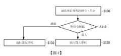
圖4說明藉由控制器140執行指令處理序列的範例。一旦經由輸入輸出緩衝器(I/O buffer)等等接收到來自外部的指令等(S100),控制器140對指令解碼(S110)。倘若指令為寫入指令,則執行寫入序列(S120);倘若指令為讀取指令,則執行讀取序列(S130)。FIG. 4 illustrates an example of the command processing sequence executed by the
在這裡,已知在可變電阻記憶體中,當SET/RESET寫入週期的數目增加時,可變電阻元件將表現得不穩定。舉例而言,當低阻抗狀態寫入時,可變電阻元件可能不會被設定至低阻抗狀態。然而,倘若可變電阻元件的資料有如此的寫入失誤時,可被修復至原始穩定狀態。Here, it is known that in a variable resistance memory, when the number of SET/RESET write cycles increases, the variable resistance element will behave unstable. For example, when writing in a low-impedance state, the variable resistance element may not be set to a low-impedance state. However, if there is such a write error in the data of the variable resistance element, it can be restored to the original stable state.
圖5A是說明SET/RESET寫入週期的數目與可變電阻元件的狀態之間關係的圖。白色圓圈相當於SET,黑色圓圈相當於RESET。圖5B是鄰近大約1.7×105週期的放大圖。在鄰近大約1.0×105週期,已知儘管寫入SET,可變電阻元件仍為高阻抗狀態。也就是說,可變電阻元件是不穩定的,具有如此失效的可變電阻元件稱為錯誤位元。需注意的是,可變電阻元件的不穩定狀態可經由重新寫入(倘若可變電阻元件於SET時失效則先RESET再SET;倘若可變電阻元件於RESET時失效則先SET再RESET)來修復成初始的穩定狀態。5A is a diagram illustrating the relationship between the number of SET/RESET write cycles and the state of the variable resistance element. The white circle is equivalent to SET, and the black circle is equivalent to RESET. FIG. 5B is an enlarged view adjacent to about 1.7×10⁵ cycles. In the vicinity of approximately 1.0×10⁵ cycles, it is known that the variable resistance element is still in a high-impedance state despite writing SET. That is, the variable resistance element is unstable, and the variable resistance element having such a failure is called an erroneous bit. It should be noted that the unstable state of the variable resistance element can be rewritten (if the variable resistance element fails during SET, then RESET and then SET; if the variable resistance element fails during RESET, then SET and then RESET) to Repair to the initial stable state.
倘若失效的記憶單元的數目,即錯誤位元的數目,超過ECC電路150可校正的位元的最大數目,則無法校正所有資料。且,錯誤位元的數目隨著循環次數上升而增加。因此,本領域的開發人員希望儘早修復錯誤位元。If the number of failed memory cells, that is, the number of erroneous bits, exceeds the maximum number of bits that can be corrected by the
因此,本實施例的RRAM 100具有修復錯誤位元的功能。具體來說,控制器140執行程式以修復錯誤位元。Therefore, the
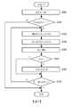
圖6是根據本發明一實施例所繪示具有可變電阻記憶體的錯誤位元修復功能的寫入操作程序的流程圖。控制器140反應於來自外部輸入的指令等開始寫入程序(S200),ECC電路150於輸入資料中執行ECC操作以產生錯誤校正碼(S210)。行選擇電路120以及列選擇電路130根據輸入位址選擇主記憶體部110A及子記憶體部110B的記憶單元,寫入驅動/讀取偏壓電路基於保留在感測放大器的資料在所選擇的記憶單元執行寫入SET或RESET(S220)。寫入驅動/讀取偏壓電路寫入例如以位元組為單位的資料至所選擇的記憶單元,感測放大器保留所寫入的資料。6 is a flowchart illustrating a write operation procedure with an error bit repair function of a variable resistance memory according to an embodiment of the invention. The
一旦完成資料寫入,接下來控制器140經由寫入驅動/讀取偏壓電路對儲存在所選擇的記憶單元的寫入資料執行驗證讀取(S230)。之後,控制器140判定寫入資料是否正確寫入(S240)。詳細而言,控制器140比較從所選擇的記憶單元讀取的資料以及輸入資料,倘若兩筆資料相符,判定寫入資料有效,倘若兩筆資料不相符,判定寫入資料失效。倘若寫入資料被判定失效,控制器140於錯誤位元旗標暫存器160中設置表示所選擇的記憶單元是錯誤位元的旗標,並於錯誤位元位址暫存器170中儲存所選擇的記憶單元的位址(S250)。另一方面,在驗證判定有效情況下,不執行步驟S250。接著,控制器140判斷輸入資料的所有位元是否都完成寫入(S260),若是則結束寫入操作程序,若否則回到步驟S220。Once the data writing is completed, the
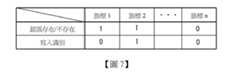
圖7說明錯誤位元旗標暫存器的儲存範例的圖。於此範例中,將可修復的錯誤位元的數目設定為n位元,因此錯誤位元旗標暫存器160儲存n個旗標,各旗標包括用以表示寫入資料是否存在錯誤的位元。本發明根據各位元的值來表示寫入資料是否失效,舉例而言,當用以表示寫入資料是否存在錯誤的位元的值為「1」時,表示對應的寫入資料出現錯誤(失效),當值為「0」時,表示對應的寫入資料沒有錯誤(即寫入正確)。再者,錯誤位元旗標暫存器160的n個旗標還包括用以表示寫入識別的位元,在本實施例中,當用以表示寫入識別的位元的值為「1」時,表示寫入SET,當值為「0」時,表示寫入RESET。於圖7的範例中,旗標1表示錯誤位元出現在所選擇的記憶單元RESET時,而旗標2表示錯誤位元出現在所選擇的記憶單元SET時,旗標n表示所選擇的記憶單元在寫入RESET時沒有出現錯誤。於本實施例中,旗標1到n的每一者具有2個位元,但可增加旗標的位元來儲存其他必須的屬性資料。FIG. 7 is a diagram illustrating a storage example of the error bit flag register. In this example, the number of repairable error bits is set to n bits, so the error bit flag register 160 stores n flags, and each flag includes a flag indicating whether there is an error in writing data Bit. The present invention indicates whether the write data is invalid according to the value of each bit. For example, when the value of the bit used to indicate whether there is an error in the write data is "1", it indicates that the corresponding write data is in error ), when the value is "0", it means that there is no error in the corresponding write data (that is, the write is correct). Furthermore, the n flags of the erroneous
圖8說明錯誤位元位址暫存器的儲存範例的圖。如圖所示,當錯誤位元旗標暫存器160所儲存的旗標表示寫入資料存在錯誤時,錯誤位元位址暫存器170將對應地儲存錯誤位元的位址。在圖7的範例中,因為在旗標1和旗標2中用以表示寫入資料是否存在錯誤的位元的值均為「1」,錯誤位元位址暫存器對應地儲存錯誤位元的位址ADxxx1、ADxxx2。FIG. 8 is a diagram illustrating a storage example of the error bit address register. As shown in the figure, when the flag stored in the error
接著,於此實施例中錯誤位元的修復操作將參考圖9的流程圖來說明。可變電阻記憶體的錯誤位元可在任何操作中被修復。於目前的實施例中,當預定事件發生時,啟動錯誤位元的修復操作。舉例而言,預定事件可為於讀取操作期間、於寫入操作期間、當電源電壓輸入時等。Next, the error bit repair operation in this embodiment will be described with reference to the flowchart of FIG. 9. The erroneous bit of the variable resistance memory can be repaired in any operation. In the current embodiment, when a predetermined event occurs, the repair operation of the error bit is started. For example, the predetermined event may be during a read operation, during a write operation, when a power supply voltage is input, and so on.
當預定事件發生時(S300),控制器140開始修復錯誤位元。預定事件例如為讀取操作。當從外部接收到讀取指令時,控制器140執行修復操作。其中,以不與預定事件衝突的方式執行修復操作。例如,在結束讀取操作後執行修復操作,或者是在讀取操作時的背景模式下同時執行修復操作。When a predetermined event occurs (S300), the
當修復操作開始時,控制器140參考錯誤位元旗標暫存器160所儲存的旗標的值以判定當前的寫入資料是否存在錯誤位元(S310)。根據圖7的示例,控制器140判斷各旗標中用以表示寫入資料存在錯誤的位元的值「1」是否存在。假如旗標中存在用以表示錯誤位元的值,控制器140控制自錯誤位元位址暫存器170讀取相應於錯誤位元的位址(S320)。接著,控制器140根據錯誤位元的位址經由行選擇電路120和列選擇電路130選擇錯誤位元,並且經由寫入驅動/讀取偏壓電路重寫錯誤位元的資料(S330)。基於如圖7所示的用以表示寫入識別的位元的值,對於寫入SET失效的錯誤位元,控制器140對錯誤位元先執行RESET再執行SET,對於寫入RESET失效的錯誤位元,控制器140對錯誤位元先執行SET再執行RESET。When the repair operation starts, the
接著,控制器140經由寫入驅動/讀取偏壓電路對錯誤位元執行驗證讀取操作(S340)。控制器140比較讀取自重寫後的錯誤位元的資料與期望值。假如讀取資料和期望值相符,控制器140判定重寫後的資料為有效,假如讀取資料和期望值不相符,控制器140判定重寫後的資料為失效(S350)。假如控制器140判定重寫後的資料為有效,由於錯誤位元已修復為可經由重寫資料而穩定儲存資料的原始記憶單元,關於錯誤位元的錯誤資訊會自錯誤位元旗標暫存器160和錯誤位元位址暫存器170清除(S360)。換句話說,於圖7的示例中,表示錯誤存在或不存在的旗標的位元清為「0」,對應的寫入識別的位元清為「0」,且將圖8中的錯誤位元位址清為「0」。另一方面,假如控制器140判定讀取資料失效,因為錯誤位元經重寫後仍是錯誤的,錯誤資訊持續保存於錯誤位元旗標暫存器160和錯誤位元位址暫存器170。Next, the
在仍然有錯誤位元作為修復目標的情況下(S370),控制器140重複上述步驟S320到S360,當沒有錯誤位元時,控制器140結束流程。In the case that there are still erroneous bits as repair targets (S370), the
於一實施例中,當控制器140判定重寫後的資料為失效,ECC電路150判斷寫入資料中經重寫後的資料為失效的數量,當經重寫後的資料為失效的數量不大於一預定值時,ECC電路150對所選擇的記憶體單元執行錯誤校正/偵測。In one embodiment, when the
如上所述,根據目前的實施例,藉由在寫入操作中保留錯誤位元的錯誤資訊,並藉由於之後的任何操作中參考錯誤資訊來重寫錯誤位元的資料,可以儘早地修復或補救錯誤位元。假如可修復的錯誤位元的數目增加,則相應地可以預期減少ECC電路150所需校正的最大位數。因此,可以抑制ECC操作帶來的性能下降,並且通過減小ECC電路耦接的區域進一步實現記憶體晶片的高度整合。As mentioned above, according to the current embodiment, by keeping in the write operationThe error information of the error bit, and by rewriting the data of the error bit by referring to the error information in any subsequent operations, the error bit can be repaired or remedied as soon as possible. If the number of repairable erroneous bits increases, then it can be expected to reduce the maximum number of correction bits required by the
後續將說明本發明的另一實施例。於上述實施例中,當預定事件出現時,修復錯誤位元。然而,寫入資料中可能存在無法再被修復的錯誤位元。換句話說,像這樣的錯誤位元的錯誤是永久性的,其中耐久性特徵完全地耗盡。Subsequently, another embodiment of the present invention will be described. In the above embodiment, when a predetermined event occurs, the erroneous bit is repaired. However, there may be erroneous bits in the written data that cannot be repaired. In other words, the error of an error bit like this is permanent, in which the durability feature is completely exhausted.
於另一實施例中,RRAM 100包括用以記錄錯誤位元的修復次數的計數器。當錯誤位元經修復後仍判定為失效,且用以記錄錯誤位元的修復次數的計數器的值已達到預設值且,控制器140清除錯誤位元旗標暫存器160和錯誤位元位址暫存器170中的錯誤資訊並且以冗餘記憶單元取代錯誤位元。冗餘記憶單元可預先準備於記憶體陣列110中。In another embodiment, the
再者,作為此實施例的改良範例,當記憶體陣列110具有用以取代難以再被修復的錯誤位元的冗餘記憶單元,可完全排除晶片上的ECC電路。換句話說,藉由修復錯誤位元以及用冗餘記憶單元取代修復次數達預定值仍無法被修復的錯誤位元,ECC電路可完全消除(即省略配置ECC電路),進而減少面積。Furthermore, as an improved example of this embodiment, when the
雖然本發明已以實施例揭露如上,然其並非用以限定本發明,任何所屬技術領域中具有通常知識者,在不脫離本發明的精神和範圍內,當可作些許的更動與潤飾,故本發明的保護範圍當視後附的申請專利範圍所界定者為準。Although the present invention has been disclosed as above with examples, it is not intended to limit theInventions, any person with ordinary knowledge in the technical field to which they belong, can make some changes and modifications without departing from the spirit and scope of the present invention. quasi.
100‧‧‧可變電阻記憶體100‧‧‧Variable resistance memory
110‧‧‧記憶體陣列110‧‧‧Memory array
110A‧‧‧主記憶體部110A‧‧‧Main Memory Department
110B‧‧‧子記憶體部110B‧‧‧Sub Memory Department
120‧‧‧行選擇電路120‧‧‧ line selection circuit
130‧‧‧列選擇電路130‧‧‧Column selection circuit
140‧‧‧控制器140‧‧‧Controller
150‧‧‧ECC電路150‧‧‧ECC circuit
160‧‧‧錯誤位元旗標暫存器160‧‧‧Error bit flag register
170‧‧‧錯誤位元位址暫存器170‧‧‧Error bit address register
Claims (11)
Translated fromChineseApplications Claiming Priority (2)
| Application Number | Priority Date | Filing Date | Title |
|---|---|---|---|
| JP2018109926AJP6612392B1 (en) | 2018-06-08 | 2018-06-08 | Semiconductor memory device |
| JP2018-109926 | 2018-06-08 |
Publications (2)
| Publication Number | Publication Date |
|---|---|
| TW202001881A TW202001881A (en) | 2020-01-01 |
| TWI690933Btrue TWI690933B (en) | 2020-04-11 |
Family
ID=68692088
Family Applications (1)
| Application Number | Title | Priority Date | Filing Date |
|---|---|---|---|
| TW108116499ATWI690933B (en) | 2018-06-08 | 2019-05-14 | Variable resistance random-access memory |
Country Status (5)
| Country | Link |
|---|---|
| US (2) | US10908989B2 (en) |
| JP (1) | JP6612392B1 (en) |
| KR (1) | KR102154436B1 (en) |
| CN (1) | CN110580927B (en) |
| TW (1) | TWI690933B (en) |
Families Citing this family (15)
| Publication number | Priority date | Publication date | Assignee | Title |
|---|---|---|---|---|
| JP6612392B1 (en)* | 2018-06-08 | 2019-11-27 | ウィンボンド エレクトロニクス コーポレーション | Semiconductor memory device |
| KR102400637B1 (en) | 2019-11-04 | 2022-05-23 | 주식회사 케이디파인켐 | Colorants for Heat Transfer Fluids and Compositions Comprising the Same |
| JP7041116B2 (en) | 2019-11-25 | 2022-03-23 | 矢崎総業株式会社 | Heat storage material composition and heat storage system for heating and cooling of buildings |
| JP2021103600A (en)* | 2019-12-25 | 2021-07-15 | ソニーセミコンダクタソリューションズ株式会社 | Storage device, storage controller and control method of storage device |
| EP3964940A4 (en) | 2020-04-01 | 2022-08-17 | Changxin Memory Technologies, Inc. | Read/write method and memory apparatus |
| CN113495671B (en) | 2020-04-01 | 2023-10-17 | 长鑫存储技术有限公司 | Read-write method and memory device |
| EP3964941B1 (en)* | 2020-04-01 | 2024-02-28 | Changxin Memory Technologies, Inc. | Read-write method and memory device |
| CN113495675B (en) | 2020-04-01 | 2023-08-11 | 长鑫存储技术有限公司 | Read-write method and memory device |
| EP3985494B1 (en) | 2020-04-01 | 2024-01-17 | Changxin Memory Technologies, Inc. | Read-write method and memory device |
| CN113495672B (en) | 2020-04-01 | 2023-08-11 | 长鑫存储技术有限公司 | Reading and writing method and memory device |
| CN113495674B (en) | 2020-04-01 | 2023-10-10 | 长鑫存储技术有限公司 | Read-write method and memory device |
| EP3936996A4 (en)* | 2020-04-01 | 2022-07-06 | Changxin Memory Technologies, Inc. | READ-WRITE METHOD AND MEMORY DEVICE |
| US11836035B2 (en)* | 2021-08-06 | 2023-12-05 | Western Digital Technologies, Inc. | Data storage device with data verification circuitry |
| JP7178465B1 (en)* | 2021-08-31 | 2022-11-25 | ウィンボンド エレクトロニクス コーポレーション | semiconductor storage device |
| FR3131400B1 (en)* | 2021-12-23 | 2024-11-08 | Commissariat Energie Atomique | Electroforming process using an inversion-invariant linear ECC and associated device. |
Citations (2)
| Publication number | Priority date | Publication date | Assignee | Title |
|---|---|---|---|---|
| US20150131383A1 (en)* | 2009-07-16 | 2015-05-14 | Mikamonu Group Ltd. | Non-volatile in-memory computing device |
| US20180158535A1 (en)* | 2016-12-07 | 2018-06-07 | Samsung Electronics Co., Ltd. | Storage device including repairable volatile memory and method of operating the same |
Family Cites Families (17)
| Publication number | Priority date | Publication date | Assignee | Title |
|---|---|---|---|---|
| KR100434315B1 (en)* | 2001-06-11 | 2004-06-05 | 주식회사 하이닉스반도체 | fail repair circuit of nonvolatile ferroelectric memory device and method for repair the same |
| JP4655000B2 (en) | 2006-08-01 | 2011-03-23 | セイコーエプソン株式会社 | Variable resistance element and resistance change type memory device |
| JP5188328B2 (en)* | 2008-08-29 | 2013-04-24 | 株式会社日立製作所 | Semiconductor device |
| JP2011181134A (en)* | 2010-02-26 | 2011-09-15 | Elpida Memory Inc | Method of controlling nonvolatile semiconductor device |
| JP5351863B2 (en) | 2010-09-17 | 2013-11-27 | シャープ株式会社 | Nonvolatile semiconductor memory device and control method of nonvolatile semiconductor memory device |
| JP5269151B2 (en)* | 2011-06-09 | 2013-08-21 | シャープ株式会社 | Semiconductor memory device |
| JP2014022004A (en)* | 2012-07-18 | 2014-02-03 | Sony Corp | Storage control device, storage device, and processing method for them |
| JP5892000B2 (en)* | 2012-08-24 | 2016-03-23 | ソニー株式会社 | STORAGE CONTROL DEVICE, NONVOLATILE MEMORY, AND MEMORY CONTROL METHOD |
| CN104008780A (en)* | 2013-02-26 | 2014-08-27 | 中芯国际集成电路制造(上海)有限公司 | Repair method and device for memory cell |
| JP5774154B1 (en)* | 2014-03-25 | 2015-09-02 | ウィンボンド エレクトロニクス コーポレーション | Resistance change memory |
| WO2016042902A1 (en)* | 2014-09-16 | 2016-03-24 | ソニー株式会社 | Memory controller, storage device, information processing system, and method for control of nonvolatile memory |
| JP6457792B2 (en)* | 2014-11-19 | 2019-01-23 | ルネサスエレクトロニクス株式会社 | Semiconductor memory device |
| RU2682387C1 (en) | 2015-03-09 | 2019-03-19 | Тосиба Мемори Корпорейшн | Semiconductor storage device |
| JP2016170848A (en)* | 2015-03-16 | 2016-09-23 | ルネサスエレクトロニクス株式会社 | Semiconductor memory device |
| CN105261392A (en)* | 2015-11-16 | 2016-01-20 | 西安华芯半导体有限公司 | Memorizing unit and method based on resistive random access memory (RRAM) |
| US9665302B1 (en)* | 2016-10-12 | 2017-05-30 | Divergent Storage Systems, Inc. | Method and apparatus for storing information using an intelligent block storage controller |
| JP6612392B1 (en)* | 2018-06-08 | 2019-11-27 | ウィンボンド エレクトロニクス コーポレーション | Semiconductor memory device |
- 2018
- 2018-06-08JPJP2018109926Apatent/JP6612392B1/enactiveActive
- 2019
- 2019-05-14TWTW108116499Apatent/TWI690933B/enactive
- 2019-05-20KRKR1020190058674Apatent/KR102154436B1/enactiveActive
- 2019-05-30CNCN201910463476.1Apatent/CN110580927B/enactiveActive
- 2019-06-05USUS16/431,739patent/US10908989B2/enactiveActive
- 2020
- 2020-12-11USUS17/118,622patent/US11494259B2/enactiveActive
Patent Citations (2)
| Publication number | Priority date | Publication date | Assignee | Title |
|---|---|---|---|---|
| US20150131383A1 (en)* | 2009-07-16 | 2015-05-14 | Mikamonu Group Ltd. | Non-volatile in-memory computing device |
| US20180158535A1 (en)* | 2016-12-07 | 2018-06-07 | Samsung Electronics Co., Ltd. | Storage device including repairable volatile memory and method of operating the same |
Also Published As
| Publication number | Publication date |
|---|---|
| JP2019212356A (en) | 2019-12-12 |
| JP6612392B1 (en) | 2019-11-27 |
| CN110580927B (en) | 2021-07-20 |
| TW202001881A (en) | 2020-01-01 |
| KR20190139760A (en) | 2019-12-18 |
| US11494259B2 (en) | 2022-11-08 |
| US10908989B2 (en) | 2021-02-02 |
| KR102154436B1 (en) | 2020-09-10 |
| US20210096947A1 (en) | 2021-04-01 |
| US20190377631A1 (en) | 2019-12-12 |
| CN110580927A (en) | 2019-12-17 |
Similar Documents
| Publication | Publication Date | Title |
|---|---|---|
| TWI690933B (en) | Variable resistance random-access memory | |
| JP6275427B2 (en) | Memory control circuit and cache memory | |
| JP3892832B2 (en) | Semiconductor memory device | |
| JP5138319B2 (en) | Memory system and operation method thereof. | |
| US8161355B2 (en) | Automatic refresh for improving data retention and endurance characteristics of an embedded non-volatile memory in a standard CMOS logic process | |
| JP4905866B2 (en) | Semiconductor memory device and operation method thereof | |
| US7861138B2 (en) | Error correction in memory devices | |
| US9760434B2 (en) | ECC method for double pattern flash memory | |
| CN110046056B (en) | Memory device for detecting and correcting data errors and method of operating the same | |
| US7385849B2 (en) | Semiconductor integrated circuit device | |
| CN116153378A (en) | Error checking and refreshing operation method and semiconductor system using the same | |
| US10229025B2 (en) | Non-volatile memory repair circuit | |
| CN116259353A (en) | Memory device and memory system performing error checking and flashing operations | |
| CN110364213B (en) | Memory system including memory device and memory controller and method of operating the same | |
| US8995217B2 (en) | Hybrid latch and fuse scheme for memory repair | |
| CN114258571B (en) | Fault tolerant memory array and method of performing error correction in a memory array | |
| US20090199043A1 (en) | Error correction in an integrated circuit with an array of memory cells | |
| US10937495B2 (en) | Resistive memory apparatus and method for writing data thereof | |
| KR20080114208A (en) | Copy-to-Program Method of Nonvolatile Memory Device with Error Correction Function | |
| JP2009043384A (en) | Nonvolatile magnetic memory device and its driving method | |
| JP2001167596A (en) | Nonvolatile semiconductor memory device | |
| JP2020187804A (en) | Data reading method for semiconductor storage device and semiconductor storage device | |
| JP2012230730A (en) | Semiconductor device |