TWI690751B - Substrate, method of producing the same and optical device - Google Patents
Substrate, method of producing the same and optical deviceDownload PDFInfo
- Publication number
- TWI690751B TWI690751BTW107125946ATW107125946ATWI690751BTW I690751 BTWI690751 BTW I690751BTW 107125946 ATW107125946 ATW 107125946ATW 107125946 ATW107125946 ATW 107125946ATW I690751 BTWI690751 BTW I690751B
- Authority
- TW
- Taiwan
- Prior art keywords
- equal
- less
- microns
- spacer
- substrate
- Prior art date
Links
- 239000000758substrateSubstances0.000titleclaimsabstractdescription75
- 230000003287optical effectEffects0.000titleclaimsabstractdescription56
- 238000000034methodMethods0.000titleclaimsdescription31
- 125000006850spacer groupChemical group0.000claimsabstractdescription254
- 239000000463materialSubstances0.000claimsdescription39
- 239000004973liquid crystal related substanceSubstances0.000claimsdescription22
- 239000004820Pressure-sensitive adhesiveSubstances0.000claimsdescription13
- 238000004519manufacturing processMethods0.000claimsdescription13
- 239000000049pigmentSubstances0.000claimsdescription11
- OKTJSMMVPCPJKN-UHFFFAOYSA-NCarbonChemical compound[C]OKTJSMMVPCPJKN-UHFFFAOYSA-N0.000claimsdescription9
- 229910052751metalInorganic materials0.000claimsdescription9
- 239000002184metalSubstances0.000claimsdescription9
- 230000001681protective effectEffects0.000claimsdescription7
- 239000006229carbon blackSubstances0.000claimsdescription4
- 150000007529inorganic basesChemical group0.000claimsdescription3
- 229910044991metal oxideInorganic materials0.000claimsdescription3
- 150000004706metal oxidesChemical class0.000claimsdescription3
- 150000004767nitridesChemical class0.000claimsdescription3
- 150000007530organic basesChemical class0.000claimsdescription3
- 229910052799carbonInorganic materials0.000claimsdescription2
- 229910002804graphiteInorganic materials0.000claimsdescription2
- 239000010439graphiteSubstances0.000claimsdescription2
- IEQIEDJGQAUEQZ-UHFFFAOYSA-NphthalocyanineChemical compoundN1C(N=C2C3=CC=CC=C3C(N=C3C4=CC=CC=C4C(=N4)N3)=N2)=C(C=CC=C2)C2=C1N=C1C2=CC=CC=C2C4=N1IEQIEDJGQAUEQZ-UHFFFAOYSA-N0.000claimsdescription2
- 239000010410layerSubstances0.000description170
- 239000010408filmSubstances0.000description62
- 230000000052comparative effectEffects0.000description22
- 239000011347resinSubstances0.000description20
- 229920005989resinPolymers0.000description20
- 239000011295pitchSubstances0.000description18
- 238000002834transmittanceMethods0.000description16
- 238000009826distributionMethods0.000description15
- 238000010586diagramMethods0.000description13
- 150000001875compoundsChemical class0.000description12
- -1poly(methyl methacrylate)Polymers0.000description12
- 210000004027cellAnatomy0.000description9
- 239000000975dyeSubstances0.000description8
- 229920000139polyethylene terephthalatePolymers0.000description8
- 239000004983Polymer Dispersed Liquid CrystalSubstances0.000description7
- 238000001723curingMethods0.000description7
- 230000014509gene expressionEffects0.000description7
- 239000005020polyethylene terephthalateSubstances0.000description7
- 229920000642polymerPolymers0.000description6
- 238000013461designMethods0.000description5
- 239000000203mixtureSubstances0.000description5
- XLOMVQKBTHCTTD-UHFFFAOYSA-NZinc monoxideChemical compound[Zn]=OXLOMVQKBTHCTTD-UHFFFAOYSA-N0.000description4
- 230000010076replicationEffects0.000description4
- 238000012360testing methodMethods0.000description4
- 239000004372Polyvinyl alcoholSubstances0.000description3
- 241000862969StellaSpecies0.000description3
- 239000003575carbonaceous materialSubstances0.000description3
- 230000000694effectsEffects0.000description3
- AMGQUBHHOARCQH-UHFFFAOYSA-Nindium;oxotinChemical compound[In].[Sn]=OAMGQUBHHOARCQH-UHFFFAOYSA-N0.000description3
- 238000002156mixingMethods0.000description3
- 229920003207poly(ethylene-2,6-naphthalate)Polymers0.000description3
- 229920003229poly(methyl methacrylate)Polymers0.000description3
- 239000011112polyethylene naphthalateSubstances0.000description3
- 239000004926polymethyl methacrylateSubstances0.000description3
- 229920002451polyvinyl alcoholPolymers0.000description3
- 238000012545processingMethods0.000description3
- NIXOWILDQLNWCW-UHFFFAOYSA-MAcrylateChemical compound[O-]C(=O)C=CNIXOWILDQLNWCW-UHFFFAOYSA-M0.000description2
- 229920002284Cellulose triacetatePolymers0.000description2
- 239000004380Cholic acidSubstances0.000description2
- 239000004696Poly ether ether ketoneSubstances0.000description2
- 239000004697PolyetherimideSubstances0.000description2
- 239000004698PolyethyleneSubstances0.000description2
- 239000004642PolyimideSubstances0.000description2
- 229920000491PolyphenylsulfonePolymers0.000description2
- 239000004743PolypropyleneSubstances0.000description2
- NNLVGZFZQQXQNW-ADJNRHBOSA-N[(2r,3r,4s,5r,6s)-4,5-diacetyloxy-3-[(2s,3r,4s,5r,6r)-3,4,5-triacetyloxy-6-(acetyloxymethyl)oxan-2-yl]oxy-6-[(2r,3r,4s,5r,6s)-4,5,6-triacetyloxy-2-(acetyloxymethyl)oxan-3-yl]oxyoxan-2-yl]methyl acetateChemical compoundO([C@@H]1O[C@@H]([C@H]([C@H](OC(C)=O)[C@H]1OC(C)=O)O[C@H]1[C@@H]([C@@H](OC(C)=O)[C@H](OC(C)=O)[C@@H](COC(C)=O)O1)OC(C)=O)COC(=O)C)[C@@H]1[C@@H](COC(C)=O)O[C@@H](OC(C)=O)[C@H](OC(C)=O)[C@H]1OC(C)=ONNLVGZFZQQXQNW-ADJNRHBOSA-N0.000description2
- 239000000853adhesiveSubstances0.000description2
- 230000001070adhesive effectEffects0.000description2
- 229910052782aluminiumInorganic materials0.000description2
- XAGFODPZIPBFFR-UHFFFAOYSA-NaluminiumChemical compound[Al]XAGFODPZIPBFFR-UHFFFAOYSA-N0.000description2
- 230000005540biological transmissionEffects0.000description2
- 239000002041carbon nanotubeSubstances0.000description2
- 229910021393carbon nanotubeInorganic materials0.000description2
- 238000012790confirmationMethods0.000description2
- 229920001577copolymerPolymers0.000description2
- 239000010949copperSubstances0.000description2
- 210000002858crystal cellAnatomy0.000description2
- 229920005994diacetyl cellulosePolymers0.000description2
- 239000006185dispersionSubstances0.000description2
- 230000005684electric fieldEffects0.000description2
- 238000009713electroplatingMethods0.000description2
- 238000011156evaluationMethods0.000description2
- 229910052737goldInorganic materials0.000description2
- 239000010931goldSubstances0.000description2
- 238000005259measurementMethods0.000description2
- 230000000704physical effectEffects0.000description2
- 239000002985plastic filmSubstances0.000description2
- 229920006255plastic filmPolymers0.000description2
- 229920002492poly(sulfone)Polymers0.000description2
- 229920001230polyarylatePolymers0.000description2
- 239000004417polycarbonateSubstances0.000description2
- 229920000515polycarbonatePolymers0.000description2
- 229920006393polyether sulfonePolymers0.000description2
- 229920002530polyetherether ketonePolymers0.000description2
- 229920001601polyetherimidePolymers0.000description2
- 229920000573polyethylenePolymers0.000description2
- 229920001721polyimidePolymers0.000description2
- 229920001155polypropylenePolymers0.000description2
- 239000011241protective layerSubstances0.000description2
- 239000000126substanceSubstances0.000description2
- 239000010409thin filmSubstances0.000description2
- 238000007740vapor depositionMethods0.000description2
- 239000011787zinc oxideSubstances0.000description2
- 229910052984zinc sulfideInorganic materials0.000description2
- PFNQVRZLDWYSCW-UHFFFAOYSA-N(fluoren-9-ylideneamino) n-naphthalen-1-ylcarbamateChemical compoundC12=CC=CC=C2C2=CC=CC=C2C1=NOC(=O)NC1=CC=CC2=CC=CC=C12PFNQVRZLDWYSCW-UHFFFAOYSA-N0.000description1
- 229910017105AlOxNyInorganic materials0.000description1
- QPLDLSVMHZLSFG-UHFFFAOYSA-NCopper oxideChemical compound[Cu]=OQPLDLSVMHZLSFG-UHFFFAOYSA-N0.000description1
- 239000005751Copper oxideSubstances0.000description1
- 229910002601GaNInorganic materials0.000description1
- JMASRVWKEDWRBT-UHFFFAOYSA-NGallium nitrideChemical compound[Ga]#NJMASRVWKEDWRBT-UHFFFAOYSA-N0.000description1
- 229920000106Liquid crystal polymerPolymers0.000description1
- 239000004721Polyphenylene oxideSubstances0.000description1
- 229910006404SnO 2Inorganic materials0.000description1
- 229910010413TiO 2Inorganic materials0.000description1
- WGLPBDUCMAPZCE-UHFFFAOYSA-NTrioxochromiumChemical compoundO=[Cr](=O)=OWGLPBDUCMAPZCE-UHFFFAOYSA-N0.000description1
- 238000003848UV Light-CuringMethods0.000description1
- 239000005083Zinc sulfideSubstances0.000description1
- GENZLHCFIPDZNJ-UHFFFAOYSA-N[In+3].[O-2].[Mg+2]Chemical compound[In+3].[O-2].[Mg+2]GENZLHCFIPDZNJ-UHFFFAOYSA-N0.000description1
- 239000002313adhesive filmSubstances0.000description1
- 239000002390adhesive tapeSubstances0.000description1
- 238000005452bendingMethods0.000description1
- 230000015572biosynthetic processEffects0.000description1
- 238000005229chemical vapour depositionMethods0.000description1
- 239000011651chromiumSubstances0.000description1
- 229910000423chromium oxideInorganic materials0.000description1
- 239000011248coating agentSubstances0.000description1
- 238000000576coating methodMethods0.000description1
- 239000003086colorantSubstances0.000description1
- 238000001816coolingMethods0.000description1
- 229910000431copper oxideInorganic materials0.000description1
- 230000006837decompressionEffects0.000description1
- 230000007547defectEffects0.000description1
- 238000000151depositionMethods0.000description1
- 230000008021depositionEffects0.000description1
- 238000009792diffusion processMethods0.000description1
- 239000002270dispersing agentSubstances0.000description1
- 150000002118epoxidesChemical class0.000description1
- 239000011521glassSubstances0.000description1
- PCHJSUWPFVWCPO-UHFFFAOYSA-NgoldChemical compound[Au]PCHJSUWPFVWCPO-UHFFFAOYSA-N0.000description1
- 229910021389grapheneInorganic materials0.000description1
- 238000010438heat treatmentMethods0.000description1
- 229910052738indiumInorganic materials0.000description1
- APFVFJFRJDLVQX-UHFFFAOYSA-Nindium atomChemical compound[In]APFVFJFRJDLVQX-UHFFFAOYSA-N0.000description1
- 239000003999initiatorSubstances0.000description1
- 230000001678irradiating effectEffects0.000description1
- 230000001788irregularEffects0.000description1
- 239000002346layers by functionSubstances0.000description1
- 238000001459lithographyMethods0.000description1
- 229910001092metal group alloyInorganic materials0.000description1
- 229910052976metal sulfideInorganic materials0.000description1
- 150000002739metalsChemical class0.000description1
- USPVIMZDBBWXGM-UHFFFAOYSA-Nnickel;oxotungstenChemical compound[Ni].[W]=OUSPVIMZDBBWXGM-UHFFFAOYSA-N0.000description1
- 150000002848norbornenesChemical class0.000description1
- KYKLWYKWCAYAJY-UHFFFAOYSA-Noxotin;zincChemical compound[Zn].[Sn]=OKYKLWYKWCAYAJY-UHFFFAOYSA-N0.000description1
- 239000002245particleSubstances0.000description1
- 238000000206photolithographyMethods0.000description1
- 230000010287polarizationEffects0.000description1
- 229920000058polyacrylatePolymers0.000description1
- 229920006267polyester filmPolymers0.000description1
- 229920000570polyetherPolymers0.000description1
- 239000002861polymer materialSubstances0.000description1
- 229920000098polyolefinPolymers0.000description1
- 238000003825pressingMethods0.000description1
- 150000003346selenoethersChemical class0.000description1
- 229910052709silverInorganic materials0.000description1
- 239000010944silver (metal)Substances0.000description1
- 229910052950sphaleriteInorganic materials0.000description1
- 239000007921spraySubstances0.000description1
- 238000004544sputter depositionMethods0.000description1
- XOLBLPGZBRYERU-UHFFFAOYSA-Ntin dioxideChemical compoundO=[Sn]=OXOLBLPGZBRYERU-UHFFFAOYSA-N0.000description1
- 229910001887tin oxideInorganic materials0.000description1
- 239000012780transparent materialSubstances0.000description1
- 239000011800void materialSubstances0.000description1
- YVTHLONGBIQYBO-UHFFFAOYSA-Nzinc indium(3+) oxygen(2-)Chemical compound[O--].[Zn++].[In+3]YVTHLONGBIQYBO-UHFFFAOYSA-N0.000description1
- DRDVZXDWVBGGMH-UHFFFAOYSA-Nzinc;sulfideChemical compound[S-2].[Zn+2]DRDVZXDWVBGGMH-UHFFFAOYSA-N0.000description1
Images


Classifications
- G—PHYSICS
- G02—OPTICS
- G02F—OPTICAL DEVICES OR ARRANGEMENTS FOR THE CONTROL OF LIGHT BY MODIFICATION OF THE OPTICAL PROPERTIES OF THE MEDIA OF THE ELEMENTS INVOLVED THEREIN; NON-LINEAR OPTICS; FREQUENCY-CHANGING OF LIGHT; OPTICAL LOGIC ELEMENTS; OPTICAL ANALOGUE/DIGITAL CONVERTERS
- G02F1/00—Devices or arrangements for the control of the intensity, colour, phase, polarisation or direction of light arriving from an independent light source, e.g. switching, gating or modulating; Non-linear optics
- G02F1/01—Devices or arrangements for the control of the intensity, colour, phase, polarisation or direction of light arriving from an independent light source, e.g. switching, gating or modulating; Non-linear optics for the control of the intensity, phase, polarisation or colour
- G02F1/13—Devices or arrangements for the control of the intensity, colour, phase, polarisation or direction of light arriving from an independent light source, e.g. switching, gating or modulating; Non-linear optics for the control of the intensity, phase, polarisation or colour based on liquid crystals, e.g. single liquid crystal display cells
- G02F1/133—Constructional arrangements; Operation of liquid crystal cells; Circuit arrangements
- G02F1/1333—Constructional arrangements; Manufacturing methods
- G02F1/1339—Gaskets; Spacers; Sealing of cells
- G02F1/13394—Gaskets; Spacers; Sealing of cells spacers regularly patterned on the cell subtrate, e.g. walls, pillars
- G—PHYSICS
- G02—OPTICS
- G02F—OPTICAL DEVICES OR ARRANGEMENTS FOR THE CONTROL OF LIGHT BY MODIFICATION OF THE OPTICAL PROPERTIES OF THE MEDIA OF THE ELEMENTS INVOLVED THEREIN; NON-LINEAR OPTICS; FREQUENCY-CHANGING OF LIGHT; OPTICAL LOGIC ELEMENTS; OPTICAL ANALOGUE/DIGITAL CONVERTERS
- G02F1/00—Devices or arrangements for the control of the intensity, colour, phase, polarisation or direction of light arriving from an independent light source, e.g. switching, gating or modulating; Non-linear optics
- G02F1/01—Devices or arrangements for the control of the intensity, colour, phase, polarisation or direction of light arriving from an independent light source, e.g. switching, gating or modulating; Non-linear optics for the control of the intensity, phase, polarisation or colour
- G02F1/13—Devices or arrangements for the control of the intensity, colour, phase, polarisation or direction of light arriving from an independent light source, e.g. switching, gating or modulating; Non-linear optics for the control of the intensity, phase, polarisation or colour based on liquid crystals, e.g. single liquid crystal display cells
- G02F1/133—Constructional arrangements; Operation of liquid crystal cells; Circuit arrangements
- G02F1/1333—Constructional arrangements; Manufacturing methods
- G02F1/1339—Gaskets; Spacers; Sealing of cells
- G02F1/13398—Spacer materials; Spacer properties
- G—PHYSICS
- G02—OPTICS
- G02F—OPTICAL DEVICES OR ARRANGEMENTS FOR THE CONTROL OF LIGHT BY MODIFICATION OF THE OPTICAL PROPERTIES OF THE MEDIA OF THE ELEMENTS INVOLVED THEREIN; NON-LINEAR OPTICS; FREQUENCY-CHANGING OF LIGHT; OPTICAL LOGIC ELEMENTS; OPTICAL ANALOGUE/DIGITAL CONVERTERS
- G02F1/00—Devices or arrangements for the control of the intensity, colour, phase, polarisation or direction of light arriving from an independent light source, e.g. switching, gating or modulating; Non-linear optics
- G02F1/01—Devices or arrangements for the control of the intensity, colour, phase, polarisation or direction of light arriving from an independent light source, e.g. switching, gating or modulating; Non-linear optics for the control of the intensity, phase, polarisation or colour
- G02F1/13—Devices or arrangements for the control of the intensity, colour, phase, polarisation or direction of light arriving from an independent light source, e.g. switching, gating or modulating; Non-linear optics for the control of the intensity, phase, polarisation or colour based on liquid crystals, e.g. single liquid crystal display cells
- G02F1/133—Constructional arrangements; Operation of liquid crystal cells; Circuit arrangements
- G02F1/1333—Constructional arrangements; Manufacturing methods
- G02F1/1335—Structural association of cells with optical devices, e.g. polarisers or reflectors
- G02F1/133509—Filters, e.g. light shielding masks
- G02F1/133512—Light shielding layers, e.g. black matrix
- G—PHYSICS
- G02—OPTICS
- G02F—OPTICAL DEVICES OR ARRANGEMENTS FOR THE CONTROL OF LIGHT BY MODIFICATION OF THE OPTICAL PROPERTIES OF THE MEDIA OF THE ELEMENTS INVOLVED THEREIN; NON-LINEAR OPTICS; FREQUENCY-CHANGING OF LIGHT; OPTICAL LOGIC ELEMENTS; OPTICAL ANALOGUE/DIGITAL CONVERTERS
- G02F1/00—Devices or arrangements for the control of the intensity, colour, phase, polarisation or direction of light arriving from an independent light source, e.g. switching, gating or modulating; Non-linear optics
- G02F1/01—Devices or arrangements for the control of the intensity, colour, phase, polarisation or direction of light arriving from an independent light source, e.g. switching, gating or modulating; Non-linear optics for the control of the intensity, phase, polarisation or colour
- G02F1/13—Devices or arrangements for the control of the intensity, colour, phase, polarisation or direction of light arriving from an independent light source, e.g. switching, gating or modulating; Non-linear optics for the control of the intensity, phase, polarisation or colour based on liquid crystals, e.g. single liquid crystal display cells
- G02F1/133—Constructional arrangements; Operation of liquid crystal cells; Circuit arrangements
- G02F1/1333—Constructional arrangements; Manufacturing methods
- G02F1/1337—Surface-induced orientation of the liquid crystal molecules, e.g. by alignment layers
- G02F1/13378—Surface-induced orientation of the liquid crystal molecules, e.g. by alignment layers by treatment of the surface, e.g. embossing, rubbing or light irradiation
- G—PHYSICS
- G02—OPTICS
- G02F—OPTICAL DEVICES OR ARRANGEMENTS FOR THE CONTROL OF LIGHT BY MODIFICATION OF THE OPTICAL PROPERTIES OF THE MEDIA OF THE ELEMENTS INVOLVED THEREIN; NON-LINEAR OPTICS; FREQUENCY-CHANGING OF LIGHT; OPTICAL LOGIC ELEMENTS; OPTICAL ANALOGUE/DIGITAL CONVERTERS
- G02F1/00—Devices or arrangements for the control of the intensity, colour, phase, polarisation or direction of light arriving from an independent light source, e.g. switching, gating or modulating; Non-linear optics
- G02F1/01—Devices or arrangements for the control of the intensity, colour, phase, polarisation or direction of light arriving from an independent light source, e.g. switching, gating or modulating; Non-linear optics for the control of the intensity, phase, polarisation or colour
- G02F1/13—Devices or arrangements for the control of the intensity, colour, phase, polarisation or direction of light arriving from an independent light source, e.g. switching, gating or modulating; Non-linear optics for the control of the intensity, phase, polarisation or colour based on liquid crystals, e.g. single liquid crystal display cells
- G02F1/133—Constructional arrangements; Operation of liquid crystal cells; Circuit arrangements
- G02F1/1333—Constructional arrangements; Manufacturing methods
- G02F1/1339—Gaskets; Spacers; Sealing of cells
- G02F1/13392—Gaskets; Spacers; Sealing of cells spacers dispersed on the cell substrate, e.g. spherical particles, microfibres
- G—PHYSICS
- G02—OPTICS
- G02F—OPTICAL DEVICES OR ARRANGEMENTS FOR THE CONTROL OF LIGHT BY MODIFICATION OF THE OPTICAL PROPERTIES OF THE MEDIA OF THE ELEMENTS INVOLVED THEREIN; NON-LINEAR OPTICS; FREQUENCY-CHANGING OF LIGHT; OPTICAL LOGIC ELEMENTS; OPTICAL ANALOGUE/DIGITAL CONVERTERS
- G02F1/00—Devices or arrangements for the control of the intensity, colour, phase, polarisation or direction of light arriving from an independent light source, e.g. switching, gating or modulating; Non-linear optics
- G02F1/01—Devices or arrangements for the control of the intensity, colour, phase, polarisation or direction of light arriving from an independent light source, e.g. switching, gating or modulating; Non-linear optics for the control of the intensity, phase, polarisation or colour
- G02F1/13—Devices or arrangements for the control of the intensity, colour, phase, polarisation or direction of light arriving from an independent light source, e.g. switching, gating or modulating; Non-linear optics for the control of the intensity, phase, polarisation or colour based on liquid crystals, e.g. single liquid crystal display cells
- G02F1/133—Constructional arrangements; Operation of liquid crystal cells; Circuit arrangements
- G02F1/1333—Constructional arrangements; Manufacturing methods
- G02F1/1343—Electrodes
- G02F1/134309—Electrodes characterised by their geometrical arrangement
- G—PHYSICS
- G02—OPTICS
- G02F—OPTICAL DEVICES OR ARRANGEMENTS FOR THE CONTROL OF LIGHT BY MODIFICATION OF THE OPTICAL PROPERTIES OF THE MEDIA OF THE ELEMENTS INVOLVED THEREIN; NON-LINEAR OPTICS; FREQUENCY-CHANGING OF LIGHT; OPTICAL LOGIC ELEMENTS; OPTICAL ANALOGUE/DIGITAL CONVERTERS
- G02F2202/00—Materials and properties
- G02F2202/04—Materials and properties dye
Landscapes
- Physics & Mathematics (AREA)
- Nonlinear Science (AREA)
- Mathematical Physics (AREA)
- Chemical & Material Sciences (AREA)
- Crystallography & Structural Chemistry (AREA)
- General Physics & Mathematics (AREA)
- Optics & Photonics (AREA)
- Liquid Crystal (AREA)
- Electrochromic Elements, Electrophoresis, Or Variable Reflection Or Absorption Elements (AREA)
- Electroluminescent Light Sources (AREA)
- Prostheses (AREA)
Abstract
Description
Translated fromChinese本申請案主張基於2017年7月27日申請的韓國專利申請案第10-2017-0095465號及2018年7月26日申請的韓國專利申請案第10-2018-0087289號的優先權權益,所述申請案的揭露內容以全文引用之方式併入本文中。This application claims priority rights based on Korean Patent Application No. 10-2017-0095465 filed on July 27, 2017 and Korean Patent Application No. 10-2018-0087289 filed on July 26, 2018. The disclosure content of the application is incorporated by reference in the text.
本申請案是關於一種基板。This application is about a substrate.
已知一種能夠藉由在彼此相對設置的基板之間設置諸如液晶化合物或液晶化合物及染料的混合物的光調變材料來調整光透射率或顏色或反射率的光學裝置。舉例而言,專利文獻1揭露所謂的應用液晶主體及二向色染料客體的混合物的賓主單元(guest host cell;GH單元)。There is known an optical device capable of adjusting light transmittance, color, or reflectance by disposing a light modulation material such as a liquid crystal compound or a mixture of liquid crystal compounds and dyes between substrates disposed opposite to each other. For example, Patent Document 1 discloses a so-called guest host cell (GH unit) using a mixture of a liquid crystal host and a dichroic dye guest.
在此類裝置中,所謂的間隔物位於基板之間以維持基板之間的間隔。In such devices, so-called spacers are located between the substrates to maintain the spacing between the substrates.
專利文獻1:歐洲專利公開案第0022311號Patent Literature 1: European Patent Publication No. 0022311
本申請案提供一種基板。本申請案的一個目的為提供具有高光學密度的黑色間隔物形成於其上的基板,其中間隔物藉由極佳黏著性黏附到基底層或基底層上的電極層且在應用至產品時並不引起諸如漏光的缺陷。本申請案的另一目的為提供一種用於製造基板的方法,此類間隔物應用至所述基板。This application provides a substrate. An object of the present application is to provide a substrate on which a black spacer with a high optical density is formed, wherein the spacer is adhered to the base layer or the electrode layer on the base layer by excellent adhesiveness and when applied to the product and Does not cause defects such as light leakage. Another object of the present application is to provide a method for manufacturing a substrate to which such a spacer is applied.
本申請案提供一種基板,包括基底層及形成於所述基底層上的黑色管柱狀間隔物且具有1.1至4範圍內的光學密度,所述黑色管柱狀間隔物的頂部為半球形。The present application provides a substrate including a base layer and a black tube column spacer formed on the base layer and having an optical density in the range of 1.1 to 4, the top of the black tube column spacer is hemispherical.
本申請案提供一種產生基板的方法,所述基板包括形成於基底層上的黑色管柱狀間隔物且具有1.1至4範圍內的光學密度,所述黑色管柱狀間隔物的頂部為半球形,所述方法包括:在形成形成於所述基底層上的所述黑色管柱狀間隔物的光可固化材料由含有遮光層的壓印罩幕來按壓的狀態下固化所述光可固化材料的步驟。含有遮光層的所述壓印罩幕具有凹面半球形形狀形成於光透射性主體的一個表面上的形式,且所述遮光薄膜形成於所述主體的表面上,所述半球形形狀並未形成於所述表面上,以及所述光可固化材料在所述凹面半球形形狀形成於其上的所述表面與所述光可固化材料緊密接觸的狀態下固化。The present application provides a method of producing a substrate including a black tube column spacer formed on a base layer and having an optical density in the range of 1.1 to 4, the top of the black tube column spacer is hemispherical The method includes curing the photocurable material in a state where the photocurable material of the black tube column spacer formed on the base layer is pressed by an imprint mask containing a light shielding layer A step of. The imprint mask screen containing the light-shielding layer has a form in which a concave hemispherical shape is formed on one surface of the light-transmitting body, and the light-shielding film is formed on the surface of the body, the hemispherical shape is not formed On the surface, and the photocurable material is cured in a state where the surface on which the concave hemispherical shape is formed is in close contact with the photocurable material.
本申請案提供一種光學裝置,包括上述的基板及第二基板,所述第二基板與所述基板相對設置且藉由所述基板中的間隔物維持與所述基板的間隙。The present application provides an optical device including the above-mentioned substrate and a second substrate, the second substrate is disposed opposite to the substrate and is separated by a gap in the substrateThe object maintains a gap with the substrate.
本申請案關於一種其上形成間隔物的基板及一種使用此類基板的光學裝置。本申請案可提供一種可應用於能夠調整光透射率、顏色及/或反射率的光學裝置的基板,因而防止在驅動裝置時出現漏光等且確保均勻光學性能。The present application relates to a substrate on which a spacer is formed and an optical device using such a substrate. The present application can provide a substrate that can be applied to an optical device capable of adjusting light transmittance, color, and/or reflectance, thereby preventing light leakage and the like while driving the device and ensuring uniform optical performance.
9:主體9: main body
100:基底層100: basal layer
200:間隔物/層200: spacer/layer
300:電極層300: electrode layer
400:壓敏黏著層400: pressure-sensitive adhesive layer
500:基底薄膜500: base film
900:罩幕900: screen
901:模具901: mold
902:遮光薄膜/黑色層902: shading film/black layer
1000:主體1000: main body
2000:遮光層2000: shading layer
3000:保護層3000: protective layer
9011:半球形形狀/凹面部分9011: Hemispherical shape/concave part
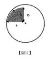
a:水平長度a: horizontal length
b:垂直長度b: vertical length
H1、H2、H3:高度H1, H2, H3: height
P:長度P: length
R:曲率半徑R: radius of curvature
W1、W2、W3:寬度W1, W2, W3: width
圖1、圖2以及圖18為本申請案的基板的形式的示意圖。1, 2 and 18 are schematic diagrams of the form of the substrate of the application.
圖3至圖12為用於說明本申請案的半球形間隔物的形狀的示意圖。3 to 12 are schematic diagrams for explaining the shape of the hemispherical spacer of the present application.
圖13為示出可用於製造本申請案的間隔物的罩幕的形狀的圖式。13 is a diagram showing the shape of a mask that can be used to manufacture the spacer of the present application.
圖14為一種使用圖13的罩幕製造間隔物的方法的示意圖。14 is a schematic diagram of a method of manufacturing a spacer using the mask of FIG. 13.
圖15及圖16為形成於間隔物上的配向薄膜的例示性橫截面的示意圖。15 and 16 are schematic cross-sectional views of the alignment film formed on the spacer.
圖17為用於說明一種實施某一不規則度的方法的圖式。FIG. 17 is a diagram for explaining a method of implementing a certain degree of irregularity.
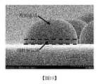
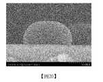
圖19及圖20為實例中所產生的半球形間隔物的相片。19 and 20 are photographs of the hemispherical spacer produced in the example.
圖21為應用於比較例的間隔物產生的罩幕的圖式。FIG. 21 is a diagram of a mask generated by a spacer applied in a comparative example.
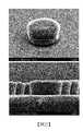
圖22及圖23為比較例中所形成的間隔物的相片。22 and 23 are photographs of the spacer formed in the comparative example.
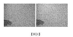
圖24至圖26為示出實例或比較例的黏著性測試結果的相片。24 to 26 are photographs showing the results of the adhesion test of examples or comparative examples.
在本說明書中所提及的物理特性中,除非另外說明,否則當所量測溫度影響結果時,相關物理特性為在室溫下量測的物理特性。術語室溫為未經加熱或冷卻的自然溫度,所述溫度可為例如10℃至30℃範圍內的任何溫度,或約23℃或約25℃左右。另外,除非本文中另外說明,否則溫度的單位為℃。Among the physical properties mentioned in this specification, unless otherwise stated, when the measured temperature affects the result, the relevant physical properties are those measured at room temperature. The term room temperature is a natural temperature without heating or cooling, and the temperature may be, for example, any temperature in the range of 10°C to 30°C, or about 23°C or about 25°C. In addition, unless otherwise stated herein, the unit of temperature is °C.
在本說明書中所提及的物理特性中,除非另外說明,否則當經量測壓力影響結果時,相關物理特性為在室內壓力下量測的物理特性。術語常壓為未經加壓或減壓的自然壓力,其中通常約1標準大氣壓被稱為常壓。Among the physical characteristics mentioned in this specification, unless otherwise stated, when the measured pressure affects the result, the relevant physical characteristics are those measured under indoor pressure. The term normal pressure is a natural pressure without pressurization or decompression, where usually about 1 standard atmospheric pressure is called normal pressure.
本申請案的基板包括基底層及存在於基底層上的間隔物。The substrate of the present application includes a base layer and a spacer existing on the base layer.
舉例而言,可在無特別侷限性的情況下應用在諸如液晶顯示器(liquid crystal display;LCD)的已知光學裝置的構形中的基板中的任何基底層來作為基底層。舉例而言,基底層可為無機基底層或有機基底層。玻璃基底層等可例示作為無機基底層,以及各種塑膠薄膜等可例示作為有機基底層。塑膠薄膜可藉由以下例示:三乙醯纖維素(triacetyl cellulose;TAC)薄膜;諸如降冰片烯衍生物的環烯共聚物(cycloolefin copolymer;COP)薄膜;諸如聚(甲基丙烯酸甲酯)(poly(methyl methacrylate);PMMA)的丙烯酸薄膜;聚碳酸酯(polycarbonate;PC)薄膜;諸如聚乙烯(polyethylene;PE)或聚丙烯(polypropylene;PP)的聚烯烴薄膜;聚乙烯醇(polyvinyl alcohol;PVA)薄膜;二乙醯基纖維素(diacetyl cellulose;DAC)薄膜;聚丙烯酸酯(polyacrylate;Pac)薄膜;聚醚碸(polyether sulfone;PES)薄膜;聚醚醚酮(polyetheretherketone;PEEK)薄膜;聚苯碸(polyphenylsulfone;PPS)薄膜、聚醚醯亞胺(polyetherimide;PEI)薄膜;聚萘二甲酸乙二酯(polyethylene naphthalate;PEN)薄膜;聚對苯二甲酸乙二酯(polyethyleneterephtalate;PET)薄膜;聚醯亞胺(polyimide;PI)薄膜;聚碸(polysulfone;PSF)薄膜或聚芳酯(polyarylate;PAR)薄膜,及其類似物,但不限於此。For example, any base layer in a substrate in the configuration of a known optical device such as a liquid crystal display (LCD) can be applied as the base layer without particular limitations. For example, the base layer may be an inorganic base layer or an organic base layer. The glass base layer and the like can be exemplified as the inorganic base layer, and various plastic films and the like can be exemplified as the organic base layer. Plastic films can be exemplified by the following: triacetyl cellulose (TAC) films; cycloolefin copolymer (COP) films such as norbornene derivatives; such as poly(methyl methacrylate) ( Poly (methyl methacrylate); PMMA acrylic film; polycarbonate (PC) film; polyolefin film such as polyethylene (PE) or polypropylene (PP); polyvinyl alcohol (polyvinyl alcohol; PVA film; diacetyl cellulose (DAC) film; polyacrylate (Pac) film; polyether (polyether)sulfone; PES film; polyetheretherketone (PEEK) film; polyphenylsulfone (PPS) film, polyetherimide (PEI) film; polyethylene naphthalate; polyethylene naphthalate; PEN) film; polyethylene terephtalate (PET) film; polyimide (PI) film; polysulfone (PSF) film or polyarylate (PAR) film, and Its analogs, but not limited to this.
在本申請案的基板中,基底層的厚度亦不受特別限制,其中可取決於應用選擇適當的範圍。In the substrate of the present application, the thickness of the base layer is also not particularly limited, and an appropriate range may be selected depending on the application.
間隔物存在於基底層上。間隔物可固定至基底層。在此情況下,間隔物可與基底層直接接觸固定,或若基底層與間隔物之間存在其他層,則其可固定於相關的其他層上。所述種類的另一層包含對於驅動光學裝置而言必要的已知層,且舉例而言,可例示在下文描述的電極層等。The spacer exists on the base layer. The spacer may be fixed to the base layer. In this case, the spacer may be fixed in direct contact with the base layer, or if there is another layer between the base layer and the spacer, it may be fixed on the other related layer. The other layer of the kind includes a known layer necessary for driving an optical device, and for example, an electrode layer described below and the like can be exemplified.
舉例而言,基板可具有電極層進一步存在於基底層與管柱狀間隔物之間的結構,且間隔物與電極層接觸。For example, the substrate may have a structure in which an electrode layer is further present between the base layer and the columnar spacer, and the spacer is in contact with the electrode layer.
圖1為間隔物200形成於基底層100上的情況的圖以及圖2為電極層300形成於基底層100上且間隔物200形成於所述基底層上的情況的圖。1 is a diagram of a case where the
在一個實例中,間隔物可為黑色管柱狀間隔物。在本申請案中,術語黑色間隔物可意謂其光學密度經量測在1.1至4範圍內的間隔物。光學密度可藉由量測黑色間隔物的透射率(單位:%)或包括與黑色間隔物相同的組件的層的透射率(單位:%)來獲得且隨後將其代入至光學密度的公式(光學密度=-log10(T),其中T為透射率)中。在本文中,包括與黑色間隔物相同的組件的層可例如藉由諸如塗佈、氣相沈積或電鍍來形成。此時,所形成的層的厚度可與黑色間隔物的高度相同,或約12微米左右。舉例而言,在所述類別的黑色間隔物中,可包含一種情況:由與黑色間隔物相同的組件所形成的具有約12微米厚度的層的光學密度在上文所提到的範圍內,實際黑色間隔物的光學密度在以上範圍內,或藉由考慮到實際黑色間隔物的厚度轉化具有約12微米厚度的層的光學密度來獲得的值在以上範圍內。此類光學密度可例如藉由用於評估以下實例或比較例中的間隔物的光學密度的方法來獲得。在另一實例中,此類光學密度可為小於或等於約3.8、小於或等於約3.6,小於或等於約3.4、小於或等於約3.2、小於或等於約3、小於或等於約2.8、小於或等於約2.6、小於或等於約2.4、小於或等於約2.2、小於或等於約2,或可為大於或等於1.2、大於或等於1.4,或大於或等於1.6。In one example, the spacer may be a black columnar spacer. In the present application, the term black spacer may mean a spacer whose optical density is measured in the range of 1.1 to 4. The optical density can be obtained by measuring the transmittance (unit: %) of the black spacer or the transmittance (unit: %) of the layer including the same components as the black spacer and then substituting it into the formula of the optical density ( Optical density = -log10 (T), where T is the transmittance). Herein, the layer including the same components as the black spacer may be formed by, for example, coating, vapor deposition, or electroplating. At this time, the thickness of the formed layer may be the same as the height of the black spacer, or about 12 microns. For example, in the category of black spacers, there may be a case where the optical density of a layer having a thickness of about 12 μm formed by the same components as the black spacer is within the range mentioned above, The optical density of the actual black spacer is within the above range, or the value obtained by converting the optical density of the layer having a thickness of about 12 microns in consideration of the thickness of the actual black spacer is within the above range. Such optical density can be obtained, for example, by a method for evaluating the optical density of the spacer in the following examples or comparative examples. In another example, such optical density may be less than or equal to about 3.8, less than or equal to about 3.6, less than or equal to about 3.4, less than or equal to about 3.2, less than or equal to about 3, less than or equal to about 2.8, less than or equal to Equal to about 2.6, less than or equal to about 2.4, less than or equal to about 2.2, less than or equal to about 2, or may be greater than or equal to 1.2, greater than or equal to 1.4, or greater than or equal to 1.6.
在能夠調整光透射率、顏色及/或反射率的光學裝置中,間隔物存在的區域成為光學非活性區,且在本申請案中,經由將上文所提及的光學密度應用至黑色間隔物,可防止在驅動裝置時出現漏光或類似現象且可確保均勻光學性能。In an optical device capable of adjusting light transmittance, color, and/or reflectance, the area where the spacer exists becomes an optically inactive area, and in the present application, by applying the above-mentioned optical density to the black space It can prevent light leakage or similar phenomena when driving the device and can ensure uniform optical performance.
此類黑色間隔物可例如藉由將能夠實現黑色的組件添加至通常用於產生管柱狀間隔物的材料來產生。Such a black spacer can be produced, for example, by adding a component capable of achieving black to the material usually used to produce the column spacer.
舉例而言,間隔物可包括能夠暗化的顏料或染料及其類似物,且具體言之,金屬氧化物、金屬氮化物、金屬氮氧化物、碳黑、石墨、偶氮類顏料、酞菁顏料或碳類材料及其類似物。鉻氧化物(Crxoy等)或銅氧化物(CuxOy等)及其類似物可例示作為上文可應用的金屬氧化物,且氮氧化鋁(AlxOyNz等)可例示作為金屬氮氧化物,但不限於此。另外,諸如碳奈米管(carbon nanotube;CNT)的多孔碳、石墨烯以及活性碳可例示作為碳類材料,但不限於此。For example, the spacer may include pigments or dyes capable of darkening and the like, and specifically, metal oxides, metal nitrides, metal oxynitrides, carbon black, graphite, azo pigments, phthalocyanine Pigments or carbon materials and the like. Chromium oxide (Crx oy, etc.) or copper oxide (Cux Oy, etc.) and the like can be exemplified as metal oxides applicable above, and aluminum oxynitride (Alx Oy Nz, etc.) It can be exemplified as the metal oxynitride, but is not limited thereto. In addition, porous carbon such as carbon nanotube (CNT), graphene, and activated carbon can be exemplified as the carbon-based material, but is not limited thereto.
舉例而言,黑色間隔物可通過組合所述材料(例如,碳類材料)連同可固化樹脂且隨後將其固化,或以適當方式將所述材料自身應用至沈積或電鍍等來製造。For example, black spacers can be manufactured by combining the materials (eg, carbon-based materials) together with curable resins and then curing them, or applying the materials themselves to deposition or electroplating, etc., in an appropriate manner.
然而,可用於本申請案中的所述類型的顏料、染料等不限於以上內容,且可取決於所需暗化(光學密度)等選擇適當類型,且亦可考慮到暗化等選擇間隔物中的比。However, the types of pigments, dyes, etc. that can be used in this application are not limited to the above, and the appropriate type may be selected depending on the desired darkening (optical density), etc., and the spacer may also be selected in consideration of darkening, etc. In the ratio.
在一個實例中,間隔物可具有1微米至50微米範圍內的高度。在另一實例中,高度可為大於或等於3微米、大於或等於5微米、大於或等於7微米、大於或等於9微米、大於或等於11微米、大於或等於13微米、大於或等於15微米、大於或等於17微米、大於或等於19微米、大於或等於21微米、大於或等於23微米、大於或等於25微米,或大於或等於27微米。在另一實例中,高度可為小於或等於48微米、小於或等於46微米、小於或等於44微米、小於或等於42微米、小於或等於40微米、小於或等於38微米、小於或等於36微米、小於或等於34微米、小於或等於32微米、小於或等於30微米、小於或等於28微米,或小於或等於26微米。In one example, the spacer may have a height in the range of 1 micrometer to 50 micrometers. In another example, the height may be greater than or equal to 3 microns, greater than or equal to 5 microns, greater than or equal to 7 microns, greater than or equal to 9 microns, greater than or equal to 11 microns, greater than or equal to 13 microns, greater than or equal to 15 microns , Greater than or equal to 17 microns, greater than or equal to 19 microns, greater than or equal to 21 microns, greater than or equal to 23 microns, greater than or equal to 25 microns, or greater than or equal to 27 microns. In another example, the height may be less than or equal to 48 microns, less than or equal to 46 microns, less than or equal to 44 microns, less than or equal to 42 microns, less than or equal to 40 microns, less than or equal to 38 microns, less than or equal to 36 microns , Less than or equal to 34 microns, less than or equal to 32 microns, less than or equal to 30 microns, less than or equal to 28 microns, or less than or equal to 26 microns.
在本申請案中,管柱狀間隔物的形狀不受特別限制,且舉例而言,圓柱形形狀,諸如三角形、四邊形、五邊形或六邊形管柱狀形狀的多邊形管柱狀形狀,或在下文描述的半球形形狀,網格形狀或其他形狀皆可適用。在一個實例中,間隔物可為半球形間隔物,半球形部分至少形成於頂部上。藉由應用具有此類半球形部分的間隔物,即使當在配向薄膜形成於上面形成有間隔物的基底層上之後執行諸如摩擦定向或光定向的定向處理時,甚至可在間隔物存在的區域中執行均勻定向處理,而不影響間隔物的步階。In the present application, the shape of the tubular column spacer is not particularly limited, and for example, a cylindrical shape, such as a polygonal tubular column shape of a triangular, quadrangular, pentagonal, or hexagonal tubular column shape, Or the hemispherical shape described below, gridShape or other shapes are applicable. In one example, the spacer may be a hemispherical spacer, and the hemispherical portion is formed at least on the top. By applying a spacer having such a hemispherical portion, even when an orientation process such as rubbing orientation or light orientation is performed after the alignment film is formed on the base layer on which the spacer is formed, even in the area where the spacer exists Perform uniform orientation processing without affecting the step of the spacer.
在本申請案中,術語半球形部分可意謂間隔物的包含其中橫截面的軌線具有預定曲率的弧形形狀的部分。另外,半球形部分的橫截面的軌線可包含曲率的中心存在於橫截面軌線內部的弧形部分。In the present application, the term hemispherical portion may mean a portion of the spacer including an arc shape in which a trajectory of a cross section has a predetermined curvature. In addition, the trajectory of the cross section of the hemispherical portion may include an arc-shaped portion whose center of curvature exists inside the trajectory of the cross section.
在一個實例中,半球形部分的橫截面軌線的最大曲率可為小於或等於2,000毫米-1。如吾人所知,曲率為表示線的曲度的數值,定義為曲率半徑的倒數,所述曲率半徑為相關曲線的預定點處的相切圓的半徑。就直線而言,曲率為0,且曲率較大,曲線的弧度越大。In one example, the maximum curvature of the cross-sectional trajectory of the hemispherical portion may be less than or equal to 2,000 mm-1 . As I know, the curvature is a numerical value representing the curvature of a line, defined as the reciprocal of the radius of curvature, which is the radius of a tangent circle at a predetermined point of the relevant curve. As far as the straight line is concerned, the curvature is 0, and the curvature is larger, the greater the curvature of the curve.
藉由控制半球形部分的彎曲程度使得半球形部分的橫截面軌線的最大曲率為小於或等於2,000毫米-1,即使當在半球形部分的頂部處執行配向薄膜的定向處理時亦可執行均勻定向處理。在本文中,用於確認半球形部分的橫截面軌線的橫截面可為基底層的任何法平面。另外,最大曲率可意謂可在半球形部分的橫截面軌線上獲得的全部相切圓的曲率之中的最大曲率。換言之,半球形部分的橫截面軌線可能不包含曲率超過2,000毫米-1的此程度的彎曲部分。By controlling the degree of bending of the hemispherical part so that the maximum curvature of the cross-sectional trajectory of the hemispherical part is less than or equal to 2,000 mm-1 , even when performing the orientation treatment of the alignment film at the top of the hemispherical part, uniform Directional processing. Herein, the cross-section used to confirm the cross-sectional trajectory of the hemispherical portion may be any normal plane of the base layer. In addition, the maximum curvature may mean the maximum curvature among the curvatures of all tangent circles that can be obtained on the cross-sectional trajectory of the hemispherical portion. In other words, the cross-sectional trajectory of the hemispherical portion may not include a curved portion with a degree of curvature exceeding 2,000 mm-1 .
在另一實例中,最大曲率可為小於或等於1,800毫米-1、小於或等於1,600毫米-1、小於或等於1,400毫米-1、小於或等於1,200毫米-1、小於或等於1,000毫米-1、小於或等於900毫米-1、小於或等於950毫米-1、小於或等於800毫米-1、小於或等於750毫米-1、小於或等於700毫米-1、小於或等於650毫米-1、小於或等於600毫米-1、小於或等於550毫米-1、小於或等於500毫米-1、小於或等於450毫米-1、小於或等於400毫米-1、小於或等於350毫米-1、小於或等於300毫米-1、小於或等於250毫米-1、小於或等於200毫米-1,或小於或等於150毫米-1左右。在另一實例中,最大曲率可為大於或等於5毫米-1、大於或等於10毫米-1、大於或等於15毫米-1、大於或等於20毫米-1、大於或等於25毫米-1、大於或等於30毫米-1、大於或等於40毫米-1、大於或等於45毫米-1,或大於或等於50毫米-1。In another example, the maximum curvature may be less than or equal to 1,800 mm-1 , less than or equal to 1,600 mm-1 , less than or equal to 1,400 mm-1 , less than or equal to 1,200 mm-1 , less than or equal to 1,000 mm-1 , Less than or equal to 900 mm-1 , less than or equal to 950 mm-1 , less than or equal to 800 mm-1 , less than or equal to 750 mm-1 , less than or equal to 700 mm-1 , less than or equal to 650 mm-1 , less than or equal to Equal to 600mm-1 , less than or equal to 550mm-1 , less than or equal to 500mm-1 , less than or equal to 450mm-1 , less than or equal to 400mm-1 , less than or equal to 350mm-1 , less than or equal to 300 Mm-1 , less than or equal to 250 mm-1 , less than or equal to 200 mm-1 , or less than or equal to about 150 mm-1 . In another example, the maximum curvature may be greater than or equal to 5 mm-1 , greater than or equal to 10 mm-1 , greater than or equal to 15 mm-1 , greater than or equal to 20 mm-1 , greater than or equal to 25 mm-1 , Greater than or equal to 30mm-1 , greater than or equal to 40mm-1 , greater than or equal to 45mm-1 , or greater than or equal to 50mm-1 .
半球形部分的橫截面軌線可包含或可不包含具有0曲率的部分,亦即,線性部分。The cross-sectional trajectory of the hemispherical portion may or may not include a portion with zero curvature, that is, a linear portion.
舉例而言,圖3為並不包含具有0曲率的部分的半球形部分的橫截面軌線的實例,以及圖4為包含具有0曲率的部分的半球形部分的橫截面軌線的實例。For example, FIG. 3 is an example of a cross-sectional trajectory of a hemispherical portion that does not include a portion with zero curvature, and FIG. 4 is an example of a cross-sectional trajectory of a hemispherical portion that includes a portion with 0 curvature.
間隔物包括如上至少在頂部的半球形部分。The spacer includes a hemispherical portion at least at the top as above.
間隔物可以各種形狀形成,只要其包括半球形部分即可。舉例而言,半球形間隔物可為半球形部分直接形成於基底層的表面上的形狀,如圖3或圖4中所示出,或可為在頂部處包含半球形部分的管柱狀間隔物,如圖5或圖6中所示出。The spacer may be formed in various shapes as long as it includes a hemispherical portion. For example, the hemispherical spacer may be a shape in which the hemispherical portion is directly formed on the surface of the base layer, as shown in FIG. 3 or FIG. 4, or may be a tubular columnar spacer including the hemispherical portion at the top Objects, as shown in Figure 5 or Figure 6.
在半球形間隔物的半球形部分中,橫截面軌線可不包含具有0曲率的部分,如圖3或圖5中所示出,或橫截面軌線亦可包含具有0曲率的部分(頂部上的平坦表面),如圖4或圖6中所示出。在下文中,為方便起見,與圖3或圖5中的間隔物的半球形部分的形狀相同的半球形部分可被稱為普通半球形部分,以及具有平坦表面形成於頂部上的半球形部分,如圖4或圖6中的間隔物的半球形部分可被稱為平坦半球形部分。In the hemispherical portion of the hemispherical spacer, the cross-sectional trajectory may not include a portion with zero curvature, as shown in FIG. 3 or FIG. 5, or the cross-sectional trajectory may also include a portion with zero curvature (on top Flat surface), as shown in Figure 4 or Figure 6show. Hereinafter, for convenience, a hemispherical part having the same shape as the hemispherical part of the spacer in FIG. 3 or FIG. 5 may be referred to as an ordinary hemispherical part, and a hemispherical part having a flat surface formed on the top The hemispherical part of the spacer as in FIG. 4 or FIG. 6 may be referred to as a flat hemispherical part.
在圖3至圖6中,H2為半球形部分的高度,R為半球形部分的曲率半徑,W1為平坦半球形部分的平坦表面的長度(寬度),W2為間隔物的寬度,H1為藉由自間隔物的總高度減去半球形部分的高度H2獲得的值。In FIGS. 3 to 6, H2 is the height of the hemispherical part, R is the radius of curvature of the hemispherical part, W1 is the length (width) of the flat surface of the flat hemispherical part, W2 is the width of the spacer, and H1 is The value obtained by subtracting the height H2 of the hemispherical portion from the total height of the spacer.
半球形部分可為完整半球形形狀或可為具有近似半球形形狀的一個半球形形狀。完整半球形形狀可為滿足下文將描述的關係式1的半球形形狀,以及近似半球形形狀可為滿足下文關係式2至關係式4中的任一者的半球形形狀。The hemispherical portion may be a complete hemispherical shape or may be a hemispherical shape having an approximate hemispherical shape. The complete hemispherical shape may be a hemispherical shape that satisfies relational expression 1 to be described below, and the approximate hemispherical shape may be a hemispherical shape that satisfies any one of relational expressions 2 to 4 below.
半球形部分可具有橫截面形狀滿足下文關係式1至關係式4中的任一者的形狀。The hemispherical portion may have a shape whose cross-sectional shape satisfies any one of Relational Expressions 1 to 4 below.
[關係式1]a=b=R[Relationship 1] a=b=R
[關係式2]a≠b=R或b≠a=R[Relationship 2] a≠b=R or b≠a=R
[關係式3]a=b<R[Relationship 3] a=b<R
[關係式4]a≠b<R[Relationship 4] a≠b<R
在關係式1至關係式4中,a為在半球形部分區段的虛擬相切圓的圓心處量測的半球形部分區段的水平長度,b為在半球形部分區段的虛擬相切圓的圓心處測量的半球形部分區段的垂直長度,以及R為半球形部分區段的虛擬相切圓的曲率半徑。In relation 1 to relation 4, a is the horizontal length of the hemispherical segment measured at the center of the virtual tangent circle of the hemispherical segment, and b is the hemisphericalThe vertical length of the semispherical partial section measured at the center of the virtual tangent circle of the partial section, and R is the radius of curvature of the virtual tangent circle of the semispherical partial section.
關係式1至關係式4中的曲率半徑對應於圖3至圖6中由R指示的長度。The radius of curvature in Relations 1 to 4 corresponds to the length indicated by R in FIGS. 3 to 6.
在關係式1至關係式4中,虛擬相切圓可意謂在與形成半球形部分的曲線相切的多個虛擬相切圓之中的具有最大曲率半徑的相切圓。In relational expressions 1 to 4, the virtual tangent circle may mean a tangent circle having the largest radius of curvature among a plurality of virtual tangent circles tangent to the curve forming the hemispherical portion.
若半球形部分為如圖3及圖5中所示出的普通半球形部分,則半球形部分整體的橫截面為曲線,且因此在與相關曲線的任何點相切的多個虛擬相切圓之中的具有最大曲率半徑的相切圓可為如關係式1至關係式4所提及的相切圓。另外,若半球形部分為如圖4及圖6中所示出的平坦半球形部分,則在與除半球形部分區段中的頂部上的平直線之外的兩側曲線的任何點相切的多個虛擬相切圓之中的具有最大曲率半徑的相切圓成為如關係式1至關係式4中所提及的虛擬相切圓。If the hemispherical part is an ordinary hemispherical part as shown in FIGS. 3 and 5, the entire cross-section of the hemispherical part is a curve, and therefore at multiple virtual tangent circles tangent to any point of the relevant curve Among them, the tangent circle having the largest radius of curvature may be a tangent circle as mentioned in relation 1 to relation 4. In addition, if the hemispherical portion is a flat hemispherical portion as shown in FIGS. 4 and 6, at any point of the curve on both sides other than the flat straight line on the top in the hemispherical portion section Among the plurality of virtual tangent circles, the tangent circle with the largest radius of curvature becomes the virtual tangent circle as mentioned in relation 1 to relation 4.
在關係式1至關係式4中,水平長度為在虛擬相切圓的中心點處在與基底層表面(圖3至圖6中的圖式元件符號100)水平的方向上所量測的長度,以及垂直長度為在與基底層表面(圖3至圖6中的圖式元件符號100)垂直的方向上所量測的長度。In relation 1 to relation 4, the horizontal length is the length measured at the center point of the virtual tangent circle in the direction horizontal to the surface of the base layer (
在關係式1至關係式4中,a為如在水平方向上進行時量測的自半球形部分區段的虛擬相切圓的圓心至半球形部分封端的點的長度。此水平長度可具有兩個長度,如在向右方向上進行時量測的距離虛擬相切圓的圓心的長度以及在向左方向上進行時量測的長度,其中關係式1至關係式4中所應用的意謂兩個長度中的較短長度。就半球形部分具有圖3及圖5的形狀而言,水平長度a為對應於間隔物的寬度W2的1/2的值。另外,在圖4及圖6的情況下,藉由將平面部分的長度(寬度)W1與兩倍的水平長度a相加獲得的值(2a+W1)可對應於間隔物的寬度W2。In relational expressions 1 to 4, a is the length from the center of the virtual tangent circle of the hemispherical portion section to the point where the hemispherical portion is terminated as measured in the horizontal direction. This horizontal length may have two lengths, such as the length of the center of the virtual tangent circle measured in the right direction and the length measured in the left direction, where relation 1 to relation 4 The meaning applied in the two lengthsShorter length. In the case where the hemispherical portion has the shapes of FIGS. 3 and 5, the horizontal length a is a value corresponding to 1/2 of the width W2 of the spacer. In addition, in the case of FIGS. 4 and 6, the value (2a+W1) obtained by adding the length (width) W1 of the planar portion to twice the horizontal length a may correspond to the width W2 of the spacer.
在關係式1至關係式4中,b為自半球形部分區段的虛擬相切圓的圓心至在垂直方向上進行時半球形部分首先相交的點的長度。通常,此垂直長度b可與半球形部分的高度(例如,由圖3至圖6中的符號H2指示的長度)大致相同。In relational expressions 1 to 4, b is the length from the center of the virtual tangent circle of the hemispherical portion section to the point where the hemispherical portion first intersects when proceeding in the vertical direction. Generally, this vertical length b may be substantially the same as the height of the hemispherical portion (for example, the length indicated by the symbol H2 in FIGS. 3 to 6).
圖7為滿足上文關係式1的半球形部分的橫截面弧形形狀,示出半球形部分的曲線具有完整圓形曲線(亦即,與虛擬相切圓的曲線一致)的情況。7 is a cross-sectional arc shape of a hemispherical part that satisfies the relationship 1 above, and shows a case where the curve of the hemispherical part has a complete circular curve (that is, a curve that coincides with a virtual tangent circle).
另外,圖8至圖12示出滿足關係式2至關係式4中的任一者的半球形部分的近似弧形形狀。In addition, FIGS. 8 to 12 show the approximate arc shape of the hemispherical portion that satisfies any one of Relational Expressions 2 to 4.
可於間隔物的底部(例如接觸基底層側面的底部)形成楔形部分,在所述楔形部分中,橫截面軌線為曲率中心形成於橫截面外部的弧形形狀。藉由此形式,根據本申請案的間隔物的特定形狀的極佳效應(例如均勻定向處理等的達成)可經進一步改善。A wedge-shaped portion may be formed at the bottom of the spacer (for example, the bottom that contacts the side of the base layer), in which the cross-sectional trajectory is an arc shape whose center of curvature is formed outside the cross-section. With this form, the excellent effect of the specific shape of the spacer according to the present application (eg, the achievement of uniform orientation processing, etc.) can be further improved.
具有與上文相同的形狀的間隔物的尺寸不受特別限制,可考慮到例如所需光學裝置的單元空隙或孔隙比等適當地選擇尺寸。The size of the spacer having the same shape as above is not particularly limited, and the size may be appropriately selected in consideration of, for example, the cell void or aperture ratio of the desired optical device.
舉例而言,半球形部分的高度(圖3至圖6中的H2)可在1微米至20微米範圍內。在另一實例中,高度可為大於或等於2微米、大於或等於3微米、大於或等於4微米、大於或等於5微米、大於或等於6微米、大於或等於7微米、大於或等於8微米、大於或等於9微米、大於或等於10微米,或大於或等於11微米。在另一實例中,高度亦可為小於或等於19微米、小於或等於18微米、小於或等於17微米、小於或等於16微米、小於或等於15微米、小於或等於14微米、小於或等於13微米、小於或等於12微米,或小於或等於11微米。For example, the height of the hemispherical portion (H2 in FIGS. 3 to 6) may be in the range of 1 micrometer to 20 micrometers. In another example, the height may be greater than or equal to 2 microns, greater than or equal to 3 microns, greater than or equal to 4 microns, greater than or equal to 5 microns, greater than or equal to 6 microns, greater than or equal to 7 microns, greater than or equal to 8 microns ,Greater than or equal to 9 microns, greater than or equal to 10 microns, or greater than or equal to 11 microns. In another example, the height may also be less than or equal to 19 microns, less than or equal to 18 microns, less than or equal to 17 microns, less than or equal to 16 microns, less than or equal to 15 microns, less than or equal to 14 microns, less than or equal to 13 Micron, less than or equal to 12 microns, or less than or equal to 11 microns.
半球形部分的寬度(圖3至圖6中的W2)可在2微米至40微米範圍內。在另一實例中,寬度可為大於或等於4微米、大於或等於6微米、大於或等於8微米、大於或等於10微米、大於或等於12微米、大於或等於14微米、大於或等於16微米、大於或等於18微米、大於或等於20微米,或大於或等於22微米。在另一實例中,寬度可為小於或等於38微米、小於或等於36微米、小於或等於34微米、小於或等於32微米、小於或等於30微米、小於或等於28微米、小於或等於26微米、小於或等於24微米,或小於或等於22微米。The width of the hemispherical portion (W2 in FIGS. 3 to 6) may be in the range of 2 to 40 microns. In another example, the width may be greater than or equal to 4 microns, greater than or equal to 6 microns, greater than or equal to 8 microns, greater than or equal to 10 microns, greater than or equal to 12 microns, greater than or equal to 14 microns, greater than or equal to 16 microns , Greater than or equal to 18 microns, greater than or equal to 20 microns, or greater than or equal to 22 microns. In another example, the width may be less than or equal to 38 microns, less than or equal to 36 microns, less than or equal to 34 microns, less than or equal to 32 microns, less than or equal to 30 microns, less than or equal to 28 microns, less than or equal to 26 microns , Less than or equal to 24 microns, or less than or equal to 22 microns.
當間隔物具有如圖3或圖4中所示出的形狀時,間隔物的高度可與半球形部分的高度相同,且當間隔物具有如圖5及圖6中所示出的形狀時,其可為藉由管柱狀部分的高度H1加上半球形部分的高度獲得的值。在一個實例中,所述高度可在1微米至50微米範圍內。When the spacer has a shape as shown in FIG. 3 or FIG. 4, the height of the spacer may be the same as the height of the hemispherical portion, and when the spacer has a shape as shown in FIGS. 5 and 6, It may be a value obtained by adding the height H1 of the columnar part of the tube to the height of the hemispherical part. In one example, the height may be in the range of 1 micrometer to 50 micrometers.
在另一實例中,高度可為大於或等於3微米、大於或等於5微米、大於或等於7微米、大於或等於9微米、大於或等於11微米、大於或等於13微米、大於或等於15微米、大於或等於17微米、大於或等於19微米、大於或等於21微米、大於或等於23微米、大於或等於25微米,或大於或等於27微米。在另一實例中,高度可為小於或等於48微米、小於或等於46微米、小於或等於44微米、小於或等於42微米、小於或等於40微米、小於或等於38微米、小於或等於36微米、小於或等於34微米、小於或等於32微米、小於或等於30微米、小於或等於28微米,或小於或等於26微米。In another example, the height may be greater than or equal to 3 microns, greater than or equal to 5 microns, greater than or equal to 7 microns, greater than or equal to 9 microns, greater than or equal to 11 microns, greater than or equal to 13 microns, greater than or equal to 15 microns , Greater than or equal to 17 microns, greater than or equal to 19 microns, greater than or equal to 21 microns, greater than or equal to 23 microns, greater than or equal to 25 microns, or greater than or equal to 27 microns. In another realFor example, the height may be less than or equal to 48 microns, less than or equal to 46 microns, less than or equal to 44 microns, less than or equal to 42 microns, less than or equal to 40 microns, less than or equal to 38 microns, less than or equal to 36 microns, less than or equal to Equal to 34 microns, less than or equal to 32 microns, less than or equal to 30 microns, less than or equal to 28 microns, or less than or equal to 26 microns.
藉由如上控制半球形間隔物或半球形管柱狀間隔物的尺寸,即使對於形成於間隔物的頂部上的配向薄膜,亦可執行均勻定向處理且可維持均勻單元空隙,且因此當基板已經應用於產生光學裝置時,相關裝置的性能可得到極好地維持。By controlling the size of the hemispherical spacer or the hemispherical tube columnar spacer as described above, even for the alignment film formed on the top of the spacer, a uniform orientation process can be performed and a uniform cell gap can be maintained, and therefore when the substrate has When applied to the production of optical devices, the performance of related devices can be excellently maintained.
間隔物可例如藉由以適合比率將上文所提及的用於暗化的染料或顏料與用於製造管柱狀間隔物等混合來產生。在一個實例中,間隔物可藉由併入紫外線可固化樹脂連同上文所提及的顏料或染料來形成。舉例而言,其可藉由在一定狀態下固化紫外線可固化化合物來形成,其中紫外線可固化化合物的形狀在能夠藉由下文將描述的壓印方法形成所需形狀的狀態下得以維持,其中紫外線固化樹脂(為紫外線可固化化合物的固化產物)可形成間隔物。可用於形成間隔物的特定種類的紫外線可固化化合物不受特別限制,且舉例而言,丙烯酸酯類聚合材料或環氧化物類聚合物等可使用,但不限於此。The spacer can be produced, for example, by mixing the above-mentioned dye or pigment for darkening with a tube-like spacer or the like for use in a suitable ratio. In one example, the spacer may be formed by incorporating an ultraviolet curable resin together with the pigment or dye mentioned above. For example, it can be formed by curing an ultraviolet curable compound in a state in which the shape of the ultraviolet curable compound can be maintained in a state where it can be formed into a desired shape by an imprint method to be described below, wherein the ultraviolet The cured resin (which is a cured product of the ultraviolet curable compound) can form a spacer. The specific kind of ultraviolet curable compound that can be used to form the spacer is not particularly limited, and for example, an acrylate-based polymer material, an epoxide-based polymer, or the like can be used, but is not limited thereto.
在本申請案中,藉由應用此類材料產生上文所描述類型的間隔物的方式不受特別限制,但為了根據所需設計內容製造具有極佳黏著性的半球形間隔物,有必要應用本文中所描述的以下壓印方法。In this application, the method of producing the spacers of the type described above by applying such materials is not particularly limited, but in order to manufacture hemispherical spacers with excellent adhesion according to the required design content, it is necessary to apply The following imprint method described in this article.
間隔物可藉由應用包含如圖13中示意性地所示出的遮光層的壓印罩幕來產生。圖13的罩幕具有以下型式:凹面半球形形狀9011形成於光透射性(例如,紫外線透射性)主體的一個表面上,且遮光薄膜902形成於其中沒有形成半球形形狀的其上形成半球形形狀9011的表面上的部分上。如圖中所示,半球形形狀9011可藉由在壓印罩幕的主體9的一個側面上形成壓印模具901及在模具901上形成半球形形狀9011及遮光薄膜902來產生。若需要,其上形成遮光薄膜902的表面可經受適當脫模處理。The spacer may include shading as shown schematically in FIG. 13 by applyingLayers of embossed masks are produced. The mask of FIG. 13 has the following type: a concave
在圖14中示出用於使用具有與上文相同形狀的罩幕產生間隔物的例示性方法。如在圖14中,將紫外線可固化化合物層200首先形成於基底層100的表面上且將罩幕900的凹面部分按壓在層200上。隨後,若所述化合物層200藉由用紫外光等照射罩幕900的頂部來固化,則化合物根據形成於罩幕900上的半球形形狀固化以形成間隔物。隨後,間隔物可藉由移除罩幕900及移除未固化化合物而以固定在基底層100上的形式得以形成。An exemplary method for creating a spacer using a mask having the same shape as above is shown in FIG. 14. As in FIG. 14, the ultraviolet
所需半球形或半球形管柱狀間隔物可藉由調整上文方法中的待照射的紫外光的量、罩幕的按壓程度及/或罩幕900的半球形形狀等來製造。The desired hemispherical or hemispherical tube-shaped spacer can be manufactured by adjusting the amount of ultraviolet light to be irradiated in the above method, the degree of pressing of the mask, and/or the hemispherical shape of the
儘管圖14示出使用用於製造半球形間隔物的罩幕的方法,如上文所描述,間隔物的形狀不受限制,且因此罩幕的形狀可根據所需間隔物的形狀而變化。Although FIG. 14 shows a method of using a mask for manufacturing a hemispherical spacer, as described above, the shape of the spacer is not limited, and thus the shape of the mask may vary according to the shape of the desired spacer.
除基底層及間隔物以外,本申請案的基板亦可包括驅動光學裝置所需的其他元件。此等元件是眾所周知的,且通常,存在電極層等。在一個實例中,基板可更包括基底層與間隔物之間的電極層。已知材料可適用於所述電極層。舉例而言,電極層可包括金屬合金、導電化合物或其兩種或超過兩種混合物。此材料可例示為:金屬,諸如金、CuI;氧化物材料,諸如氧化銦錫(indium tin oxide;ITO)、氧化銦鋅(indium zinc oxide;IZO)、氧化鋅錫(zinc tin oxide;ZTO)、摻雜有鋁或銦的鋅氧化物、氧化鎂銦、氧化鎳鎢、ZnO、SnO2或In2O3;金屬氮化物,諸如氮化鎵;金屬硒化物,諸如硒化鋅;金屬硫化物,諸如硫化鋅;或類似物。透明的正電洞噴射電極層亦可藉由使用Au、Ag或Cu的金屬薄膜等與具有高折射率的透明材料(諸如ZnS、TiO2或ITO)的層合物形成。In addition to the base layer and the spacer, the substrate of the present application may also include other elements required to drive the optical device. Such elements are well known, and generally, there are electrode layers and the like. In one example, the substrate may further include an electrode layer between the base layer and the spacer. Known materials may be suitable for the electrode layer. For example, the electrode layer may include a metal alloy, a conductive compound, or a mixture of two or more of them. This material can be exemplified by: metals such as gold, CuI; oxide materials such as indium tin oxide (ITO), indium zinc oxide (IZO), zinc tin oxide (ZTO) , Zinc oxide doped with aluminum or indium, magnesium indium oxide, nickel tungsten oxide, ZnO, SnO2 or In2 O3 ; metal nitrides such as gallium nitride; metal selenides such as zinc selenide; metal sulfide Substances, such as zinc sulfide; or the like. The transparent positive hole spray electrode layer can also be formed by a laminate of a metal thin film using Au, Ag, or Cu and a transparent material having a high refractive index (such as ZnS, TiO2 or ITO).
電極層可藉由諸如氣相沈積、濺鍍、化學氣相沈積或電化學手段的任何手段形成。亦可以已知方式在無任何特別限制的情況下圖案化電極層,且所述電極層可例如經由已知光微影或一種使用蔭罩幕或類似物的方法加以圖案化。The electrode layer may be formed by any means such as vapor deposition, sputtering, chemical vapor deposition, or electrochemical means. The electrode layer can also be patterned in a known manner without any particular restrictions, and the electrode layer can be patterned, for example, by known photolithography or a method using a shadow mask or the like.
本申請案的基板可更包括存在於基底層及間隔物上的配向薄膜。The substrate of the present application may further include an alignment film existing on the base layer and the spacer.
因此,本申請案的另一例示性基板可包括基底層;存在於基底層上的間隔物;以及形成於基底層及間隔物上的配向薄膜。Therefore, another exemplary substrate of the present application may include a base layer; a spacer existing on the base layer; and an alignment film formed on the base layer and the spacer.
在本文中,基底層及間隔物的細節如上文所描述。Herein, the details of the base layer and the spacer are as described above.
另外,形成於基底層及間隔物上的所述配向薄膜的種類不受特別限制,其中已知配向薄膜,例如已知摩擦配向薄膜或光配向薄膜可適用。In addition, the kind of the alignment film formed on the base layer and the spacer is not particularly limited, and known alignment films, for example, known friction alignment films or optical alignment films are applicable.
於基底層及間隔物上形成配向薄膜及在其上執行定向處理的方法亦是根據已知方法。The method of forming the alignment film on the base layer and the spacer and performing the orientation process thereon are also according to known methods.
然而,若在一個實例中,配向薄膜形成於上文所描述的半球形間隔物上,則配向薄膜亦可具有取決於間隔物的形狀的獨特形狀。圖15為示意性地示出此類配向薄膜的橫截面軌線的圖。圖15為形成於間隔物上的配向薄膜的橫截面形狀的實例,其中頂部示出曲率中心形成於橫截面的內側上同時具有預定的寬度W3及高度H3的半球形形狀。However, if in one example, the alignment film is formed on the hemispherical spacer described above, the alignment film may also have a unique shape depending on the shape of the spacershape. FIG. 15 is a diagram schematically showing the cross-sectional trajectory of such an alignment film. 15 is an example of the cross-sectional shape of the alignment film formed on the spacer, in which the top shows a hemispherical shape in which the center of curvature is formed on the inner side of the cross-section while having a predetermined width W3 and height H3.
舉例而言,配向薄膜亦可包括上文所描述的頂部上的半球形部分。在此情況下,半球形部分可具有小於或等於2,000毫米-1的橫截面軌線的最大曲率。在另一實例中,最大曲率可為小於或等於1,800毫米-1、小於或等於1,600毫米-1、小於或等於1,400毫米-1、小於或等於1,200毫米-1、小於或等於1,000毫米-1、小於或等於900毫米-1、小於或等於950毫米-1、小於或等於800毫米-1、小於或等於750毫米-1、小於或等於700毫米-1、小於或等於650毫米-1、小於或等於600毫米-1、小於或等於550毫米-1、小於或等於500毫米-1、小於或等於450毫米-1、小於或等於400毫米-1、小於或等於350毫米-1、小於或等於300毫米-1、小於或等於250毫米-1、小於或等於200毫米-1,或小於或等於150毫米-1左右。在另一實例中,最大曲率可為大於或等於5毫米-1、大於或等於10毫米-1、大於或等於15毫米-1、大於或等於20毫米-1、大於或等於25毫米-1、大於或等於30毫米-1、大於或等於40毫米-1、大於或等於45毫米-1,或大於或等於50毫米-1。For example, the alignment film may also include the hemispherical portion on the top described above. In this case, the hemispherical portion may have a maximum curvature of a cross-sectional trajectory of less than or equal to 2,000 mm-1 . In another example, the maximum curvature may be less than or equal to 1,800 mm-1 , less than or equal to 1,600 mm-1 , less than or equal to 1,400 mm-1 , less than or equal to 1,200 mm-1 , less than or equal to 1,000 mm-1 , Less than or equal to 900 mm-1 , less than or equal to 950 mm-1 , less than or equal to 800 mm-1 , less than or equal to 750 mm-1 , less than or equal to 700 mm-1 , less than or equal to 650 mm-1 , less than or equal to Equal to 600mm-1 , less than or equal to 550mm-1 , less than or equal to 500mm-1 , less than or equal to 450mm-1 , less than or equal to 400mm-1 , less than or equal to 350mm-1 , less than or equal to 300 Mm-1 , less than or equal to 250 mm-1 , less than or equal to 200 mm-1 , or less than or equal to 150 mm-1 . In another example, the maximum curvature may be greater than or equal to 5 mm-1 , greater than or equal to 10 mm-1 , greater than or equal to 15 mm-1 , greater than or equal to 20 mm-1 , greater than or equal to 25 mm-1 , Greater than or equal to 30 mm-1 , greater than or equal to 40 mm-1 , greater than or equal to 45 mm-1 , or greater than or equal to 50 mm-1 .
配向薄膜的半球形部分的橫截面軌線可包含或可不包含具有0曲率的部分,亦即,線性部分。The cross-sectional trajectory of the hemispherical portion of the alignment film may or may not include a portion having a curvature of 0, that is, a linear portion.
形成於如上間隔物上的配向薄膜的高度及寬度亦根據存在於底部上的間隔物的高度與寬度及所形成配向薄膜的厚度等來判定,其不受特別限制。The height and width of the alignment film formed on the above spacer are also determined based on the height and width of the spacer existing on the bottom and the thickness of the alignment film formed, etc., and are not particularly limited.
舉例而言,半球形部分的高度(圖15中的H3)可在1微米至50微米範圍內。在另一實例中,高度可為大於或等於2微米、大於或等於3微米、大於或等於4微米、大於或等於5微米、大於或等於6微米、大於或等於7微米、大於或等於8微米、大於或等於9微米、大於或等於10微米,或大於或等於11微米。在另一實例中,高度亦可為小於或等於48微米、小於或等於46微米、小於或等於44微米、小於或等於42微米、小於或等於40微米、小於或等於38微米、小於或等於36微米、小於或等於34微米、小於或等於32微米、小於或等於30微米、小於或等於28微米、小於或等於26微米、小於或等於24微米、小於或等於22微米、小於或等於19微米、小於或等於18微米、小於或等於17微米、小於或等於16微米、小於或等於15微米、小於或等於14微米、小於或等於13微米、小於或等於12微米,或小於或等於11微米。For example, the height of the hemispherical portion (H3 in FIG. 15) may be in the range of 1 micrometer to 50 micrometers. In another example, the height may be greater than or equal to 2 microns, greater than or equal to 3 microns, greater than or equal to 4 microns, greater than or equal to 5 microns, greater than or equal to 6 microns, greater than or equal to 7 microns, greater than or equal to 8 microns , Greater than or equal to 9 microns, greater than or equal to 10 microns, or greater than or equal to 11 microns. In another example, the height may also be less than or equal to 48 microns, less than or equal to 46 microns, less than or equal to 44 microns, less than or equal to 42 microns, less than or equal to 40 microns, less than or equal to 38 microns, less than or equal to 36 Microns, less than or equal to 34 microns, less than or equal to 32 microns, less than or equal to 30 microns, less than or equal to 28 microns, less than or equal to 26 microns, less than or equal to 24 microns, less than or equal to 22 microns, less than or equal to 19 microns, Less than or equal to 18 microns, less than or equal to 17 microns, less than or equal to 16 microns, less than or equal to 15 microns, less than or equal to 14 microns, less than or equal to 13 microns, less than or equal to 12 microns, or less than or equal to 11 microns.
另外,半球形部分的寬度(圖15中的W3)可在1微米至80微米範圍內。在另一實例中,寬度可為大於或等於2微米、大於或等於3微米、大於或等於4微米、大於或等於6微米、大於或等於8微米、大於或等於10微米、大於或等於12微米、大於或等於14微米、大於或等於16微米、大於或等於18微米、大於或等於20微米,或大於或等於22微米。在另一實例中,寬度可為小於或等於78微米、小於或等於76微米、小於或等於74微米、小於或等於72微米、小於或等於70微米、小於或等於68微米、小於或等於66微米、小於或等於64微米、小於或等於60微米、小於或等於58微米、小於或等於56微米、小於或等於54微米、小於或等於52微米、小於或等於50微米、小於或等於48微米、小於或等於46微米、小於或等於44微米、小於或等於42微米、小於或等於40微米、小於或等於38微米、小於或等於36微米、小於或等於34微米、小於或等於32微米、小於或等於30微米、小於或等於28微米、小於或等於26微米、小於或等於24微米或小於或等於22微米。In addition, the width of the hemispherical portion (W3 in FIG. 15) may be in the range of 1 micrometer to 80 micrometers. In another example, the width may be greater than or equal to 2 microns, greater than or equal to 3 microns, greater than or equal to 4 microns, greater than or equal to 6 microns, greater than or equal to 8 microns, greater than or equal to 10 microns, greater than or equal to 12 microns , Greater than or equal to 14 microns, greater than or equal to 16 microns, greater than or equal to 18 microns, greater than or equal to 20 microns, or greater than or equal to 22 microns. In another example, the width can be less than or equal to 78 microns, less than or equal to 76 microns, less than or equal to 74 microns, less than or equal to 72 microns, less than or equal to 70 microns, less than or equal to 68 microns, less than or equal to 66 microns , Less than or equal to 64 microns, less than or equal to 60 microns, less than or equal to 58 microns, less than or equal to 56 microns, less than or equal to 54 micronsMeters, less than or equal to 52 microns, less than or equal to 50 microns, less than or equal to 48 microns, less than or equal to 46 microns, less than or equal to 44 microns, less than or equal to 42 microns, less than or equal to 40 microns, less than or equal to 38 microns, Less than or equal to 36 microns, less than or equal to 34 microns, less than or equal to 32 microns, less than or equal to 30 microns, less than or equal to 28 microns, less than or equal to 26 microns, less than or equal to 24 microns or less than or equal to 22 microns.
就本申請案的基板而言,可藉由將間隔物的形狀調整成獨特半球形形狀而均勻地執行形成於間隔物上的配向薄膜的定向處理,而不受間隔物的步階影響。For the substrate of the present application, the alignment process of the alignment film formed on the spacer can be uniformly performed by adjusting the shape of the spacer to a unique hemispherical shape without being affected by the steps of the spacer.
為了使此效應最大化,配向薄膜的形狀可經進一步控制。In order to maximize this effect, the shape of the alignment film can be further controlled.
舉例而言,如同配向薄膜的橫截面所示出於圖15及圖16中,自配向薄膜的橫截面中的與基板層接觸的點面向上的區域可為其中曲率中心形成於橫截面外部的弧形形狀,其中曲率半徑R1及曲率半徑R2為由配向薄膜的曲線形狀形成的兩個圓的曲率半徑。此形狀可例如根據間隔物的形狀及配向薄膜的形成條件來形成。因此,即使當對配向薄膜執行諸如摩擦處理的定向處理時,可執行並未受間隔物的步階影響的均勻定向處理。For example, as shown in the cross-sections of the alignment film in FIGS. 15 and 16, the area of the cross-section of the self-alignment film in which the point in contact with the substrate layer faces upward may be a center in which the center of curvature is formed outside the cross-section In an arc shape, the radius of curvature R1 and the radius of curvature R2 are the radius of curvature of two circles formed by the curved shape of the alignment film. This shape can be formed, for example, according to the shape of the spacer and the formation conditions of the alignment film. Therefore, even when an orientation process such as a rubbing process is performed on the alignment film, a uniform orientation process that is not affected by the steps of the spacer can be performed.
基底層可藉由包括相同或不同間隔物(包含如上文所提及的半球形間隔物)而包括多個間隔物。此類多個間隔物可設置在基底層上,同時具有預定規則性及不規則性。特定而言,就經排列以具有彼此不同的間距而言,基底層上的多個間隔物中的至少一部分可呈不規則排列,但就經排列而在區域之間具有根據預定規則測定的實質上相同密度而言可為規則的。The base layer may include a plurality of spacers by including the same or different spacers (including hemispherical spacers as mentioned above). Such a plurality of spacers may be provided on the base layer while having predetermined regularity and irregularity. In particular, in terms of being arranged to have different pitches from each other, at least a part of the plurality of spacers on the base layer may be irregularly arranged, but in terms of being arranged to have the substance determined according to a predetermined rule between regions The same density can be regular.
亦即,在一個實例中,設置於基底層上的間隔物中的至少一部分可經設置以具有彼此不同的間距。That is, in one example, at least the spacer provided on the base layerA part may be set to have a different pitch from each other.
在本文中,當已選擇多個間隔物中的一部分以按其他間隔物不存在於閉合圖形中的狀態來形成閉合圖形時,術語間距可定義為閉合圖形的側邊的長度。另外,除非另外說明,否則間距的單位為微米。Herein, when a part of the plurality of spacers has been selected to form a closed figure in a state where other spacers are not present in the closed figure, the term pitch may be defined as the length of the side of the closed figure. In addition, unless otherwise stated, the unit of the pitch is micrometers.
因此形成的閉合圖形可為三角形、四邊形或六邊形。亦即,當已視情況選擇多個間隔物之中的三個間隔物且使其彼此連接時,形成三角形;當已選擇四個間隔物且使其彼此連接時,形成四邊形;且當已選擇六個間隔物且連接時,形成六邊形。The closed figure thus formed may be triangular, quadrilateral or hexagonal. That is, when three spacers among the plurality of spacers have been selected and connected to each other, a triangle is formed; when four spacers have been selected and connected to each other, a quadrilateral is formed; and when selected When six spacers are connected, they form a hexagon.
舉例而言,若存在於基底層上的間隔物之中的四個間隔物視情況選擇且由假想線(虛線)連接,則形成為閉合圖形的四邊形。形成在確定間距時形成的閉合圖形,使得其中不存在間隔物,且舉例而言,若構成閉合圖形的間隔物形成使得其中存在另一間隔物,則其並非判定間距的閉合圖形。For example, if four spacers among the spacers present on the base layer are selected as appropriate and connected by an imaginary line (dashed line), they are formed as a closed-shaped quadrilateral. A closed figure formed when determining the pitch is formed so that there is no spacer therein, and for example, if the spacer constituting the closed figure is formed so that another spacer exists therein, it is not a closed figure for determining the pitch.
在一個實例中,為因此形成的閉合圖形的三角形、四邊形或六邊形的側邊之中具有相同長度的側邊的數目的比率(%)(就三角形而言,100×(長度相同的側邊的數目)/3;就四邊形而言,100×(長度相同的側邊的數目)/4;且就六邊形而言,100×(長度相同的側邊的數目)/6)可為小於或等於85%。在另一實例中,所述比率可小於或等於84%、小於或等於80%、小於或等於76%、小於或等於67%、小於或等於55%,或小於或等於40%。所述比率的下限不受特別限制。亦即,在一些情況下,由於閉合圖形的全部側邊的長度可能不相同,所述比率的下限可為0%。In one example, the ratio (%) of the number of sides having the same length among the sides of the triangle, quadrangle, or hexagon of the closed figure thus formed (in terms of triangles, 100×(sides of the same length Number of sides)/3; for quadrilaterals, 100×(number of sides with the same length)/4; and for hexagons, 100×(number of sides with the same length)/6) can be Less than or equal to 85%. In another example, the ratio may be less than or equal to 84%, less than or equal to 80%, less than or equal to 76%, less than or equal to 67%, less than or equal to 55%, or less than or equal to 40%. The lower limit of the ratio is not particularly limited. That is, in some cases, since the length of all sides of the closed figure may be different, the lower limit of the ratio may be 0%.
如上文所描述,本申請案的間隔物的排列不規則,因為其至少部分具有不同間距,但此不規則性受控於某種規則性。在本文中,所述規則性可意謂間隔物的排列密度在某些區域之間實質上彼此接近。As described above, the arrangement of the spacers in this application is irregular becauseAt least some have different pitches, but this irregularity is controlled by some regularity. Here, the regularity may mean that the arrangement density of the spacers is substantially close to each other between certain regions.
舉例而言,若多個不規則排列的間隔物的正常間距為P,則當已在基底層的表面上視情況選擇以10P作為單側長度的兩個或超過兩個正方形區域時,存在於每一正方形區域中的間隔物的數目的標準偏差小於或等於2。For example, if the normal spacing of a plurality of irregularly arranged spacers is P, when two or more than two square regions with 10P as a single side length have been selected on the surface of the base layer as appropriate, exist in The standard deviation of the number of spacers in each square area is less than or equal to 2.
在本文中,術語正常間距意謂在實際上不規則地設置在基底層上的多個間隔物因考慮到間隔物的數目及基底層的面積而經置放使得幾乎所有間隔物以相同間距設置的狀態下,鄰近間隔物的中心之間的距離。In this context, the term normal pitch means that a plurality of spacers that are irregularly arranged on the base layer in practice are placed so that almost all the spacers are arranged at the same pitch due to the number of spacers and the area of the base layer The distance between the centers of adjacent spacers.
已知確認全部上文提及的間隔物經設置以具有相同間距的虛擬狀態的方式,其可藉由使用諸如CAD、MATLAB、STELLA或Excel的隨機數產生程式來達成。It is known to confirm that all the above-mentioned spacers are set in a virtual state with the same pitch, which can be achieved by using a random number generation program such as CAD, MATLAB, STELLA, or Excel.
標準偏差為表示數個間隔物的分散程度的數值,其為藉由分散度的正平方根測定的數值。The standard deviation is a numerical value indicating the degree of dispersion of several spacers, which is a value measured by the positive square root of the degree of dispersion.
亦即,當已在其上形成有間隔物的基底層的表面上視情況指定至少兩個或超過兩個矩形區域且隨後已獲得存在於所述區域中的間隔物的數目的標準偏差時,標準偏差小於或等於2。在另一實例中,標準偏差可為小於或等於1.5、小於或等於1或小於或等於0.5。另外,標準偏差意謂數值越低,所需規則性越容易達成,且因此所述下限不受特別限制,其可為例如0。That is, when at least two or more than two rectangular regions are optionally designated on the surface of the base layer on which the spacers have been formed and then the standard deviation of the number of spacers present in the regions has been obtained, The standard deviation is less than or equal to 2. In another example, the standard deviation may be less than or equal to 1.5, less than or equal to 1 or less than or equal to 0.5. In addition, the standard deviation means that the lower the numerical value, the easier the required regularity is achieved, and therefore the lower limit is not particularly limited, and it may be, for example, 0.
在本文中,指定矩形區域的數目不受特別限制,只要其大於或等於2即可,但在一個實例中,所述數目可經選擇作為在基底層的表面上視情況經選擇以免彼此重疊的矩形區域的數目,其限制條件為視情況選擇的區域所佔據的面積為基底層的總面積的大於或等於約10%、大於或等於20%、大於或等於30%、大於或等於40%、大於或等於50%、大於或等於60%、大於或等於70%、大於或等於80%或大於或等於90%。In this article, the number of designated rectangular areas is not particularly limited as long as it is greater than or equal to 2, but in one example, the number can be selected as the baseThe number of rectangular areas that are optionally selected on the surface of the bottom layer to avoid overlapping each other is limited by the area occupied by the selected area being greater than or equal to about 10% of the total area of the base layer, greater than or equal to 20%, Greater than or equal to 30%, greater than or equal to 40%, greater than or equal to 50%, greater than or equal to 60%, greater than or equal to 70%, greater than or equal to 80% or greater than or equal to 90%.
形成任意矩形區域的單側的正常間距(P)的範圍可藉由存在於基底層上的間隔物的數目及相關基底層的面積測定,如上文所描述,所述間距不受特別限制,且通常,其可在100微米至1,000微米的範圍內。The range of the normal pitch (P) on one side forming an arbitrary rectangular area can be determined by the number of spacers present on the base layer and the area of the related base layer, as described above, the pitch is not particularly limited, and Generally, it may be in the range of 100 microns to 1,000 microns.
儘管不受特別限制,但如上存在於視情況選擇的正方形區域中的間隔物的平均數目可為例如約80至150左右。在另一實例中,平均數目可為大於或等於82、大於或等於84、大於或等於86、大於或等於88、大於或等於90、大於或等於92、大於或等於94、大於或等於96,或大於或等於98。而且,在另一實例中,平均數目可為小於或等於148、小於或等於146、小於或等於144、小於或等於142、小於或等於140、小於或等於138、小於或等於136、小於或等於134、小於或等於132、小於或等於130、小於或等於128、小於或等於126、小於或等於124、小於或等於122、小於或等於120、小於或等於118、小於或等於116、小於或等於114,或小於或等於112。Although not particularly limited, the average number of spacers present in the square area selected as above may be, for example, about 80 to 150 or so. In another example, the average number may be greater than or equal to 82, greater than or equal to 84, greater than or equal to 86, greater than or equal to 88, greater than or equal to 90, greater than or equal to 92, greater than or equal to 94, greater than or equal to 96, Or greater than or equal to 98. Moreover, in another example, the average number may be less than or equal to 148, less than or equal to 146, less than or equal to 144, less than or equal to 142, less than or equal to 140, less than or equal to 138, less than or equal to 136, less than or equal to 134, less than or equal to 132, less than or equal to 130, less than or equal to 128, less than or equal to 126, less than or equal to 124, less than or equal to 122, less than or equal to 120, less than or equal to 118, less than or equal to 116, less than or equal to 114, or less than or equal to 112.
而且,上文所提及的標準偏差(SD)與間隔物的平均數目(A)的比(SD/A)可為小於或等於0.1。在另一實例中,所述比可為小於或等於0.09、小於或等於0.08、小於或等於0.07、小於或等於0.06、小於或等於0.05、小於或等於0.04,或小於或等於0.03。Moreover, the ratio (SD/A) of the standard deviation (SD) mentioned above to the average number of spacers (A) may be less than or equal to 0.1. In another example, the ratio may be less than or equal to 0.09, less than or equal to 0.08, less than or equal to 0.07, less than or equal to 0.06, less than or equal to 0.05, less than or equal to 0.04, or less than or etc.于0.03.
可視情況改變所述平均數目(A)或所述比(SD/A),且舉例而言,可考慮到透射率、單元間隙及/或應用基板的裝置中所需單元間隙的均勻性及類似因素而改變所述數值。The average number (A) or the ratio (SD/A) can be changed as appropriate, and for example, the uniformity of the cell gap and the like required in the transmittance, cell gap, and/or device using the substrate can be considered Factors to change the value.
在另一實例中,當其上形成有不規則設置的間隔物的基底層的表面已劃分成兩個或超過兩個具有相同面積的區域時,每一單元區域中的間隔物的數目的標準偏差可為小於或等於2。In another example, when the surface of the base layer on which irregularly arranged spacers are formed has been divided into two or more regions with the same area, the standard for the number of spacers in each unit region The deviation can be less than or equal to 2.
在本文中,標準偏差的含義及其特定實例如上文所描述。In this document, the meaning of standard deviation and its specific examples are as described above.
亦即,在所述實例中,當基底層已劃分成至少兩個具有相同面積的區域,且已獲得存在於每一經劃分單元區域中的間隔物的數目的標準偏差時,其標準偏差小於或等於2。在此情況下,每一經劃分單元區域的形狀不受特別限制,只要相關單元區域經劃分以具有相同面積即可,但其可為例如三角形、正方形或六邊形區域。另外,在另一實例中,以上狀態下的標準偏差可為小於或等於1.5、小於或等於1,或小於或等於0.5,且如上文所描述,其下限值不受特別限制,可為例如0。That is, in the example, when the base layer has been divided into at least two regions having the same area, and the standard deviation of the number of spacers present in each divided unit region has been obtained, the standard deviation is less than or Equal to 2. In this case, the shape of each divided unit area is not particularly limited as long as the related unit area is divided to have the same area, but it may be, for example, a triangular, square, or hexagonal area. In addition, in another example, the standard deviation in the above state may be less than or equal to 1.5, less than or equal to 1, or less than or equal to 0.5, and as described above, the lower limit value thereof is not particularly limited, and may be, for example 0.
在本文中,單元區域的數目不受特別限制,但在一個實例中,基底層可劃分成兩個或超過兩個、四個或超過四個、六個或超過六個、八個或超過八個、或十個或超過十個具有相同面積的區域。在本文中,由於經劃分區域的數目越大意謂著維持的間隔物密度越均勻,故經劃分區域的數目的上限不受特別限制。Here, the number of unit regions is not particularly limited, but in one example, the base layer may be divided into two or more than two, four or more than four, six or more than six, eight or more than eight , Or ten or more than ten areas with the same area. Herein, since the larger the number of divided regions means the more uniform the spacer density is maintained, the upper limit of the number of divided regions is not particularly limited.
當已在基板上選擇以正常間距P作為單側的虛擬正方形區域(多個間隔物設置於所述基板上以便同時具有規則性及不規則性)時,存在於相關區域中的間隔物的平均數目可在0至4的範圍內。在另一實例中,平均數目可為小於或等於3.5、小於或等於3、小於或等於2.5、小於或等於2,或小於或等於1.5。而且,在另一實例中,平均數目可為大於或等於0.5。在本文中,其單側長度視情況經指定為正常間距(P)的正方形區域的數目不受特別限制,只要其為兩個或超過兩個即可,但在一個實例中,所述數目可經選擇作為在基底層的表面上視情況經選擇以免彼此重疊的正方形區域的數目,其限制條件為視情況選擇的區域所佔據的面積為基底層的總面積的大於或等於約10%、大於或等於20%、大於或等於30%、大於或等於40%、大於或等於50%、大於或等於60%、大於或等於70%、大於或等於80%或大於或等於90%。When a virtual square area with a normal pitch P as one side has been selected on the substrate (multiple spacers are provided on the substrate to have both regularity and irregularity), the average of the spacers present in the relevant area The number can be between 0 and 4Within range. In another example, the average number may be 3.5 or less, 3 or less, 2.5 or less, 2 or less, or 1.5 or less. Moreover, in another example, the average number may be greater than or equal to 0.5. In this context, the number of square areas whose one-sided length is optionally designated as the normal pitch (P) is not particularly limited as long as it is two or more than two, but in one example, the number may be It is selected as the number of square regions optionally selected on the surface of the base layer so as not to overlap with each other. The limitation is that the area occupied by the area selected as appropriate is greater than or equal to about 10% of the total area of the base layer. 20% or more, 30% or more, 40% or more, 50% or more, 60% or more, 70% or more, 80% or more, or 90% or more.
多個間隔物的整體密度可經調節使得間隔物所佔據的面積相對於基底層的總面積的比率為小於或等於約50%。在另一實例中,所述比率可能小於或等於約45%、小於或等於約40%、小於或等於約35%、小於或等於約30%、小於或等於約25%、小於或等於約20%、小於或等於約15%、小於或等於約10%、小於或等於約9.5%、小於或等於9%、小於或等於8.5%、小於或等於8%、小於或等於7.5%、小於或等於7%、小於或等於6.5%、小於或等於6%、小於或等於5.5%、小於或等於5%、小於或等於4.5%、小於或等於4%、小於或等於3.5%、小於或等於3%、小於或等於2.5%、小於或等於2%,或小於或等於1.5%。在另一實例中,所述比率可能大於或等於約0.1%、大於或等於0.2%、大於或等於0.3%、大於或等於0.4%、大於或等於0.5%、大於或等於0.6%、大於或等於0.7%、大於或等於0.8%、大於或等於0.9%,或大於或等於0.95%。The overall density of the plurality of spacers may be adjusted so that the ratio of the area occupied by the spacers to the total area of the base layer is less than or equal to about 50%. In another example, the ratio may be less than or equal to about 45%, less than or equal to about 40%, less than or equal to about 35%, less than or equal to about 30%, less than or equal to about 25%, less than or equal to about 20 %, less than or equal to about 15%, less than or equal to about 10%, less than or equal to about 9.5%, less than or equal to 9%, less than or equal to 8.5%, less than or equal to 8%, less than or equal to 7.5%, less than or equal to 7%, 6.5% or less, 6% or less, 5.5% or less, 5% or less, 4.5% or less, 4% or less, 3.5% or less, 3% or less , Less than or equal to 2.5%, less than or equal to 2%, or less than or equal to 1.5%. In another example, the ratio may be greater than or equal to about 0.1%, greater than or equal to 0.2%, greater than or equal to 0.3%, greater than or equal to 0.4%, greater than or equal to 0.5%, greater than or equal to 0.6%, greater than or equal to 0.7%, greater than or equal to 0.8%, greater than or equal to 0.9%, or greater than or equal to 0.95%.
當已藉由以上文形式於基底層上設置多個間隔物而實現光學裝置時,可確保均勻光學特性而不造成所謂的波紋現象,同時所述間隔物維持基板之間的均勻間距(單元間隙)。When it has been achieved by placing multiple spacers on the base layer in the above formIn the case of an optical device, it is possible to ensure uniform optical characteristics without causing so-called moiré phenomenon, and at the same time, the spacer maintains a uniform interval (cell gap) between substrates.
可在必要時改變各別數值,且舉例而言,可考慮到透射率、單元間隙及/或應用基板的裝置中所需單元間隙的均勻性及類似因素而改變所述數值。The respective numerical values may be changed as necessary, and for example, the numerical values may be changed in consideration of the transmittance, the cell gap, and/or the uniformity of the required cell gap in the device to which the substrate is applied, and the like.
多個間隔物可經排列使得其間隔常態分佈圖表示預定形狀。The plurality of spacers may be arranged so that the interval normal distribution diagram represents a predetermined shape.
在本文中,間隔常態分佈圖為展示作為X軸的間隔物之間的間距以及作為Y軸的所有間隔物之中具有相關間距的間隔物的比率的分佈圖,其中間隔物的比率為在全部間隔物的數目為1時所獲得的比率。In this article, the interval normal distribution diagram is a distribution diagram showing the spacing between the spacers as the X axis and the ratio of the spacers with the relevant spacing among all the spacers as the Y axis, where the ratio of the spacers is The ratio obtained when the number of spacers is one.
本說明書中與本文中之間隔常態分佈圖相關的間距為三角形、四邊形或六邊形中的側邊的長度,所述形狀為上文提及的閉合圖形。In this specification, the pitch associated with the interval normal distribution diagram herein is the length of the side in a triangle, quadrangle, or hexagon, which is the closed figure mentioned above.
所述分佈圖可藉由使用已知隨機數座標程式,例如CAD、MATLAB或STELLA隨機數座標程式或類似程式獲得。The distribution map can be obtained by using a known random number coordinate program, such as CAD, MATLAB, or STELLA random number coordinate program or the like.
在一個實例中,多個間隔物可經設置使得分佈圖中的半高面積在0.4至0.95範圍內。在另一實例中,半高面積可為大於或等於0.6、大於或等於0.7或大於或等於0.85。而且,在另一實例中,所述半高面積可為小於或等於0.9、小於或等於0.85、小於或等於0.8、小於或等於0.75、小於或等於0.7、小於或等於0.65、小於或等於0.6、小於或等於0.55、或小於或等於0.5。In one example, the plurality of spacers may be set so that the half-height area in the distribution map is in the range of 0.4 to 0.95. In another example, the half-height area may be greater than or equal to 0.6, greater than or equal to 0.7, or greater than or equal to 0.85. Moreover, in another example, the half-height area may be less than or equal to 0.9, less than or equal to 0.85, less than or equal to 0.8, less than or equal to 0.75, less than or equal to 0.7, less than or equal to 0.65, less than or equal to 0.6, Less than or equal to 0.55, or less than or equal to 0.5.
多個間隔物可經排列使得分佈圖中的半高寬(FWHM)與平均間距(Pm)的比(FWHM/Pm)小於或等於1。在另一實例中,所述比(FWHM/Pm)可為大於或等於0.05、大於或等於0.1、大於或等於0.11、大於或等於0.12,或大於或等於0.13。而且,在另一實例中,所述比(FWHM/Pm)為小於或等於約0.95、小於或等於約0.9、小於或等於約0.85、小於或等於約0.8、小於或等於約0.75、小於或等於約0.7、小於或等於約0.65、小於或等於約0.6、小於或等於約0.55、小於或等於約0.5、小於或等於約0.45,或小於或等於約0.4。The plurality of spacers may be arranged so that the ratio of full width at half maximum (FWHM) to average pitch (Pm) (FWHM/Pm) in the distribution map is less than or equal to 1. In another example,The ratio (FWHM/Pm) may be greater than or equal to 0.05, greater than or equal to 0.1, greater than or equal to 0.11, greater than or equal to 0.12, or greater than or equal to 0.13. Moreover, in another example, the ratio (FWHM/Pm) is less than or equal to about 0.95, less than or equal to about 0.9, less than or equal to about 0.85, less than or equal to about 0.8, less than or equal to about 0.75, less than or equal to About 0.7, less than or equal to about 0.65, less than or equal to about 0.6, less than or equal to about 0.55, less than or equal to about 0.5, less than or equal to about 0.45, or less than or equal to about 0.4.
當已選擇至少80%或大於80%、大於或等於85%、大於或等於90%、或大於或等於95%的間隔物來形成為上文所描述的閉合圖形的三角形、四邊形或六邊形時,上文提及的平均間距(Pm)為由所選間隔物形成的三角形、四邊形或六邊形的各別側邊的長度的平均值。在本文中,間隔物亦經選擇使得形成的三角形、四邊形或六邊形彼此不會共用頂點。When a spacer of at least 80% or greater than 80%, greater than or equal to 85%, greater than or equal to 90%, or greater than or equal to 95% has been selected to form the triangle, quadrilateral or hexagon of the closed graph described above At this time, the above-mentioned average pitch (Pm) is the average of the lengths of the respective sides of the triangle, quadrangle, or hexagon formed by the selected spacer. Herein, the spacers are also selected so that the triangles, quadrilaterals or hexagons formed do not share vertices with each other.
多個間隔物可經設置使得分佈圖中的半高寬(FWHM)在0.5微米至1,000微米範圍內。在另一實例中,所述半高寬(FWHM)可為大於或等於約1微米、大於或等於2微米、大於或等於3微米、大於或等於4微米、大於或等於5微米、大於或等於6微米、大於或等於7微米、大於或等於8微米、大於或等於9微米、大於或等於10微米、大於或等於11微米、大於或等於12微米、大於或等於13微米、大於或等於14微米、大於或等於15微米、大於或等於16微米、大於或等於17微米、大於或等於18微米、大於或等於19微米、大於或等於20微米、大於或等於21微米、大於或等於22微米、大於或等於23微米或大於或等於24微米。在另一實例中,所述半高寬(FWHM)可為小於或等於約900微米、小於或等於800微米、小於或等於700微米、小於或等於600微米、小於或等於500微米、小於或等於400微米、小於或等於300微米、小於或等於200微米、小於或等於150微米、小於或等於100微米、小於或等於90微米、小於或等於80微米、小於或等於70微米、小於或等於60微米、小於或等於50微米、小於或等於40微米、或小於或等於30微米。The plurality of spacers may be set so that the full width at half maximum (FWHM) in the distribution pattern is in the range of 0.5 micrometer to 1,000 micrometers. In another example, the full width at half maximum (FWHM) may be greater than or equal to about 1 micron, greater than or equal to 2 microns, greater than or equal to 3 microns, greater than or equal to 4 microns, greater than or equal to 5 microns, greater than or equal to 6 microns, greater than or equal to 7 microns, greater than or equal to 8 microns, greater than or equal to 9 microns, greater than or equal to 10 microns, greater than or equal to 11 microns, greater than or equal to 12 microns, greater than or equal to 13 microns, greater than or equal to 14 microns , Greater than or equal to 15 microns, greater than or equal to 16 microns, greater than or equal to 17 microns, greater than or equal to 18 microns, greater than or equal to 19 microns, greater than or equal to 20 microns, greater than or equal to 21 microns, greater than or equal to 22 microns, greater than Or equal to 23 microns or greater than or equal to 24 microns. In another example, the full width at half maximum (FWHM) may be less than or equal to about 900 microns,Less than or equal to 800 microns, less than or equal to 700 microns, less than or equal to 600 microns, less than or equal to 500 microns, less than or equal to 400 microns, less than or equal to 300 microns, less than or equal to 200 microns, less than or equal to 150 microns, less than or equal to Equal to 100 microns, less than or equal to 90 microns, less than or equal to 80 microns, less than or equal to 70 microns, less than or equal to 60 microns, less than or equal to 50 microns, less than or equal to 40 microns, or less than or equal to 30 microns.
所述多個間隔物可經設置使得間隔常態分佈圖的最大高度(Fmax)為大於或等於0.006且小於1。在另一實例中,最大高度(Fmax)可為大於或等於約0.007、大於或等於約0.008、大於或等於約0.009,或大於或等於約0.0095。而且,在另一實例中,所述最大高度(Fmax)可為小於或等於約0.9、小於或等於約0.8、小於或等於約0.7、小於或等於約0.6、小於或等於約0.5、小於或等於約0.4、小於或等於約0.3、小於或等於約0.2、小於或等於約0.1、小於或等於約0.09、小於或等於約0.08、小於或等於約0.07、小於或等於約0.06、小於或等於約0.05、小於或等於約0.04、小於或等於約0.03,或小於或等於約0.02。The plurality of spacers may be set so that the maximum height (Fmax) of the space normal distribution map is greater than or equal to 0.006 and less than 1. In another example, the maximum height (Fmax) may be greater than or equal to about 0.007, greater than or equal to about 0.008, greater than or equal to about 0.009, or greater than or equal to about 0.0095. Moreover, in another example, the maximum height (Fmax) may be less than or equal to about 0.9, less than or equal to about 0.8, less than or equal to about 0.7, less than or equal to about 0.6, less than or equal to about 0.5, less than or equal to About 0.4, less than or equal to about 0.3, less than or equal to about 0.2, less than or equal to about 0.1, less than or equal to about 0.09, less than or equal to about 0.08, less than or equal to about 0.07, less than or equal to about 0.06, less than or equal to about 0.05 , Less than or equal to about 0.04, less than or equal to about 0.03, or less than or equal to about 0.02.
當已藉由以此類形式設置多個間隔物以便具有所述間隔常態分佈圖來實現光學裝置時,可確保均勻光學特性而不造成所謂的波紋現象,同時間隔物維持基板之間的均勻間距(單元間隙)。When an optical device has been realized by providing a plurality of spacers in such a form so as to have the space normal distribution pattern, uniform optical characteristics can be ensured without causing a so-called ripple phenomenon, while the spacers maintain a uniform spacing between substrates (Cell gap).
針對待如上設置以便同時具有不規則性及規則性的多個間隔物引入不規則度的概念。在下文中,將描述一種用於設計具有此類形式的間隔物的排列的方法。The concept of irregularity is introduced for a plurality of spacers to be set as above so as to have irregularity and regularity at the same time. Hereinafter, a method for designing an arrangement of spacers having such a form will be described.
為達成同時具有上文提及的規則性及不規則性的間隔物的排列,執行自正常排列狀態開始並重新定位間隔物以具有不規則性的步驟。In order to achieve the arrangement of the spacers having both the regularity and irregularity mentioned above, the execution starts from the normal arrangement state and repositions the spacers to have irregularitiesRegular steps.
在本文中,正常排列狀態為多個間隔物經設置在基底層上以使得可形成全部側邊具有相同長度的等邊三角形、正方形或等邊六邊形的狀態。圖17為間隔物經設置以形成例如正方形的狀態。在此狀態下的正方形的單側的長度P可等於上文提及的正常間距。在此類排列狀態下,基於其中存在一個間隔物的點,指定具有半徑長度與單側的長度P成比例的圓形區域,且設定程式以使得所述一個間隔物可在區域中隨機移動。舉例而言,圖17示意性地展示以下形式:其中設定半徑長度相對於長度P為50%(0.5P)的圓形區域,且間隔物移動至所述區域中的任何點。上文所描述的排列可藉由對至少80%或大於80%、大於或等於85%、大於或等於90%、大於或等於95%或100%(全部間隔物)的間隔物施加此類移動來達成。Here, the normal arrangement state is a state in which a plurality of spacers are arranged on the base layer so that an equilateral triangle, a square, or an equilateral hexagon with all sides having the same length can be formed. FIG. 17 is a state where the spacer is provided to form, for example, a square. The length P of one side of the square in this state may be equal to the normal pitch mentioned above. In such an arrangement state, based on a point where there is a spacer, a circular area having a radius length proportional to the length P on one side is specified, and a formula is set so that the one spacer can move randomly in the area. For example, FIG. 17 schematically shows the following form: a circular area in which the radius length is set to 50% (0.5P) with respect to the length P, and the spacer moves to any point in the area. The arrangement described above can be applied by applying such movement to spacers of at least 80% or greater than 80%, greater than or equal to 85%, greater than or equal to 90%, greater than or equal to 95% or 100% (all spacers) To achieve.
在此類設計方法中,變成圓形區域的半徑的長度P的比率可定義為不規則度。舉例而言,在圖17中所展示的情況下,不規則度為約50%。In such a design method, the ratio of the length P of the radius that becomes a circular area can be defined as an irregularity. For example, in the case shown in FIG. 17, the degree of irregularity is about 50%.
在一個實例中,所述設計方式中的不規則度可為大於或等於約5%、大於或等於約10%、大於或等於約15%、大於或等於約20%、大於或等於約25%、大於或等於約30%、大於或等於約35%、大於或等於約40%、大於或等於約45%、大於或等於約50%、大於或等於約55%、大於或等於約60%,或大於或等於約65%。在一個實例中,不規則度可為小於或等於約95%、小於或等於約90%、小於或等於約85%、或小於或等於約80%。In one example, the irregularity in the design may be greater than or equal to about 5%, greater than or equal to about 10%, greater than or equal to about 15%, greater than or equal to about 20%, greater than or equal to about 25% , Greater than or equal to about 30%, greater than or equal to about 35%, greater than or equal to about 40%, greater than or equal to about 45%, greater than or equal to about 50%, greater than or equal to about 55%, greater than or equal to about 60%, Or greater than or equal to about 65%. In one example, the degree of irregularity may be less than or equal to about 95%, less than or equal to about 90%, less than or equal to about 85%, or less than or equal to about 80%.
同時具有上文所描述的不規則性及規則性的排列可藉由以與上文相同的方式設計間隔物的排列並根據所述經設計排列形成間隔物來達成。The arrangement of irregularities and regularities described above can be achieved byThe arrangement of the spacers is designed in the same manner as above, and the spacers are formed according to the designed arrangement.
而且,在本文中,儘管已例示正常狀態自正方形開始的情況,但正常狀態可為其他圖形,諸如等邊三角形或等邊六邊形,且在此情況下,亦可達成上文所描述的排列。Moreover, in this article, although the normal state has been exemplified from the square, the normal state may be other figures, such as an equilateral triangle or an equilateral hexagon, and in this case, the above description can also be achieved arrangement.
此外,用於以與上文相同的方式設計間隔物的排列的手段不受特別限制,且可使用已知隨機數座標程式,諸如CAD、MATLAB、STELLA或Excel隨機數座標程式。In addition, the means for designing the arrangement of the spacers in the same manner as above is not particularly limited, and a known random number coordinate program such as CAD, MATLAB, STELLA, or Excel random number coordinate program can be used.
舉例而言,在首先以與上文相同的方式設計間隔物的排列之後,可製造具有根據相關設計的圖案的罩幕等,且此類間隔物可藉由將相關罩幕應用至上文所描述的微影或壓印方法及類似方法來實施。For example, after first designing the arrangement of the spacers in the same manner as above, a mask or the like having a pattern according to the relevant design can be manufactured, and such spacers can be applied by applying the relevant mask to the description above Lithography or imprinting methods and similar methods to implement.
本申請案的間隔物對基底層或間隔物接觸的基底層的元件(例如,電極層)展現極佳黏著性。The spacer of the present application exhibits excellent adhesion to the base layer or the element (eg, electrode layer) of the base layer that the spacer contacts.
舉例而言,即使具有約3.72牛頓/10毫米至4.16牛頓/10毫米的剝離力的壓敏黏著劑膠帶黏附於其上形成間隔物的基底層的表面且黏著劑膠帶經剝離,間隔物的圖案可基本上維持而不損失。此時,壓敏黏著劑膠帶可為例如被稱為米其邦(Nichiban)膠帶CT-24的膠帶。米其邦膠帶具有約3.72牛頓/10毫米至4.16牛頓/10毫米的剝離力,如根據JIS Z 1522標準以180度的剝離角度所量測。藉由將米其邦膠帶CT-24黏附至其上形成間隔物的基底層的表面且隨後在縱向方向上以約30毫米/秒的剝離速率及約180度的剝離角度剝離米其邦膠帶CT-24所量測的間隔物的損失率可為小於或等於15%、小於或等於13%、小於或等於11%、小於或等於9%、小於或等於8%、小於或等於7%、小於或等於6%、小於或等於5%、小於或等於4%、小於或等於3%、小於或等於2%、小於或等於1%,或小於或等於0.5%,矩形黏附面積具有24毫米的寬度及40毫米的長度。在本文中,損失率可為在剝離壓敏黏著劑膠帶之後已經損失的間隔物的數目相對於存在於黏附面積內的所有間隔物的數目的百分比。取決於所應用的用途,通常10,000個至40,000個間隔物可存在於以上黏附面積中,其中此等間隔物之中將損失的間隔物的比率可維持在以上範圍內。For example, even if a pressure-sensitive adhesive tape having a peeling force of about 3.72 N/10 mm to 4.16 N/10 mm is adhered to the surface of the base layer on which the spacer is formed and the adhesive tape is peeled off, the pattern of the spacer Can be basically maintained without loss. At this time, the pressure-sensitive adhesive tape may be, for example, a tape called CT-24 of Nichiban tape. Michelbond tape has a peel force of about 3.72 Newtons/10 mm to 4.16 Newtons/10 mm, as measured at a peel angle of 180 degrees according to the JIS Z 1522 standard. By adhering the Michelbon tape CT-24 to the surface of the base layer on which the spacer is formed and then peeling the Michelbon tape CT in the longitudinal direction at a peeling rate of about 30 mm/sec and a peeling angle of about 180 degrees -24 The measured loss rate of the spacer can be less than or equal to 15%, less than or equal to 13%, less than or equal to 11%, less than orEqual to 9%, less than or equal to 8%, less than or equal to 7%, less than or equal to 6%, less than or equal to 5%, less than or equal to 4%, less than or equal to 3%, less than or equal to 2%, less than or equal to 1 %, or less than or equal to 0.5%, the rectangular adhesion area has a width of 24 mm and a length of 40 mm. Here, the loss rate may be a percentage of the number of spacers that have been lost after peeling the pressure-sensitive adhesive tape relative to the number of all spacers present in the adhesion area. Depending on the application used, generally 10,000 to 40,000 spacers may be present in the above adhesion area, wherein the ratio of spacers to be lost among such spacers may be maintained within the above range.
就黑色間隔物而言,為了滿足上文所提及的光學密度,包含諸如染料或顏料的暗化材料,其中間隔物材料的固化速率由於此類暗化材料受到抑制,使得極難形成如上具有極佳黏著性的間隔物。然而,以本申請案中所提及的方式產生的間隔物可具有極佳黏著性,同時由於其特定半球形形狀及製造方法而具有上文所描述的光學密度。In the case of black spacers, in order to satisfy the optical density mentioned above, darkening materials such as dyes or pigments are included, wherein the curing rate of the spacer material is suppressed due to such darkening materials, making it extremely difficult to form as above Excellent adhesive spacer. However, the spacers produced in the manner mentioned in the present application may have excellent adhesion, while having the optical density described above due to their specific hemispherical shape and manufacturing method.
當間隔物呈現此黏著性時,所述間隔物即使在配向薄膜形成於間隔物的表面上且諸如摩擦的定向處理執行的情況下可穩定地維持,使得有可能最後製造具有極佳性能的產品。另外,其上形成間隔物的基板可在保護性壓敏黏著劑薄膜黏附於其上形成間隔物的表面直至其應用至實際產品的狀態下得以維持,其中在此類結構中,圖案即使在壓敏黏著劑薄膜剝離時可穩定地維持而不損失。When the spacer exhibits this adhesiveness, the spacer can be stably maintained even when an alignment film is formed on the surface of the spacer and an orientation process such as friction is performed, making it possible to finally manufacture a product with excellent performance . In addition, the substrate on which the spacer is formed can be maintained in a state where the protective pressure-sensitive adhesive film is adhered to the surface on which the spacer is formed until it is applied to the actual product, wherein in such a structure, the pattern is even pressed The sensitive adhesive film can be stably maintained without loss when peeled off.
在一個實例中,所述基板可包括保護膜作為額外構形。舉例而言,所述基板可更包括黏附於其中形成間隔物的基底層的表面的保護性壓敏黏著劑薄膜。作為以上構形中的壓敏黏著劑薄膜,已知保護性壓敏黏著劑薄膜可使用而無任何特別侷限性。In one example, the substrate may include a protective film as an additional configuration. For example, the substrate may further include a protective pressure-sensitive adhesive film adhered to the surface of the base layer in which the spacer is formed. As the pressure-sensitive adhesive film in the above configuration,It is known that a protective pressure-sensitive adhesive film can be used without any particular limitation.
圖18為保護性薄膜黏附於圖2中所示出的基板上的形式,其中保護性薄膜通常包括基底薄膜500及形成於其一個表面上的壓敏黏著層400。18 is a form in which a protective film is adhered to the substrate shown in FIG. 2, where the protective film generally includes a
本申請案亦關於一種用於產生所述基板的方法。所述產生方法可包括在光可固化材料由含有遮光層的壓印罩幕按壓的狀態下固化用於形成形成於基底層上的黑色管柱狀間隔物的光可固化材料的步驟。上文所應用的所述類型的光可固化材料不受特別限制,其中可使用已知黑色管柱狀間隔物材料且在一個實例中,可使用藉由將諸如顏料或染料的暗化材料與紫外線可固化樹脂混合獲得的材料。The present application also relates to a method for producing the substrate. The production method may include a step of curing the photo-curable material for forming the black tube-shaped spacer formed on the base layer in a state where the photo-curable material is pressed by the imprint mask screen containing the light-shielding layer. The photocurable material of the type applied above is not particularly limited, in which known black tube column spacer materials can be used and in one example, by darkening materials such as pigments or dyes and Material obtained by mixing ultraviolet curable resin.
此外,可使用例如圖13中所例示性示出的罩幕作為包含遮光層的壓印罩幕。因此,包含遮光層的壓印罩幕可具有凹面半球形形狀(圖13中的9011)形成於光透射性主體(圖13中的9)的一個表面上且遮光薄膜(圖13中的902)形成於半球形形狀並非形成於其上形成半球形形狀的側面中的表面上的形式,且如上文參考圖14所描述,光可固化材料可在其上如上罩幕的凹面半球形形狀形成的表面與光可固化材料緊密接觸的狀態下固化。In addition, for example, a mask screen exemplarily shown in FIG. 13 may be used as the imprint mask screen including the light shielding layer. Therefore, the imprint mask including the light-shielding layer may have a concave hemispherical shape (9011 in FIG. 13) formed on one surface of the light-transmitting body (9 in FIG. 13) and the light-shielding film (902 in FIG. 13) The form formed in the hemispherical shape is not a form formed on the surface in the side on which the hemispherical shape is formed, and as described above with reference to FIG. 14, the photocurable material may be formed thereon as the concave hemispherical shape of the upper mask The surface is cured in close contact with the photocurable material.
此時,電極層形成於基底層上,其中光可固化材料可形成於電極層上。At this time, the electrode layer is formed on the base layer, wherein the photocurable material may be formed on the electrode layer.
上文方法中所形成的凹面部分的規格(例如,直徑或高度等)不受特別限制且其可根據所需半球形形狀形成。亦即,由於上文所描述的半球形形狀的高度、寬度等大致遵循著罩幕的凹面部分的形狀,半球形形狀可經由此控制。而且另外,可考慮所使用的材料調整待照射的例如紫外光的光的量。The specifications (eg, diameter or height, etc.) of the concave portion formed in the above method are not particularly limited and it may be formed according to a desired hemispherical shape. That is, since the height, width, etc. of the hemispherical shape described above roughly follow the shape of the concave portion of the mask, the hemispherical shape can be controlled via this. And in addition, consider the use ofThe material adjusts the amount of light to be irradiated, such as ultraviolet light.
本申請案亦有關於一種使用此基板形成的光學裝置。This application also relates to an optical device formed using this substrate.
本申請案的例示性光學裝置可包括所述基板以及第二基板,所述第二基板與所述基板相對設置且藉由所述基板中的間隔物維持與所述基板間隙。An exemplary optical device of the present application may include the substrate and a second substrate, the second substrate being disposed opposite to the substrate and maintaining a gap with the substrate by a spacer in the substrate.
在所述光學裝置中,光調變層可存在於兩個基板之間的間隙中。在本申請案中,術語光調變層可包含所有已知類型的能夠取決於用途改變諸如偏光狀態、透射率、色調及入射光反射率的特性之中的至少一個特性的層。In the optical device, the light modulation layer may exist in the gap between the two substrates. In the present application, the term light modulation layer may include all known types of layers capable of changing at least one of characteristics such as polarization state, transmittance, hue, and incident light reflectance depending on the use.
舉例而言,光調變層為包括液晶材料的層,其可為藉由電壓的開關(例如垂直電場或水平電場)在漫射模式與透射模式之間切換的液晶層、在透射模式與阻斷模式之間切換的液晶層、在透明模式與彩色模式之間切換的液晶層、或在不同色彩的彩色模式之間切換的液晶層。For example, the light modulation layer is a layer including a liquid crystal material, which may be a liquid crystal layer that switches between a diffusion mode and a transmission mode by a voltage switch (such as a vertical electric field or a horizontal electric field), and the transmission mode and the resistance The liquid crystal layer switched between the off mode, the liquid crystal layer switched between the transparent mode and the color mode, or the liquid crystal layer switched between the color modes of different colors.
能夠執行如上操作的光調變層,例如液晶層是眾所周知的。可使用典型液晶顯示器中使用的液晶層作為一個例示性光調變層。在另一實例中,光調變層亦可為各種類型的所謂的賓主液晶層、聚合物分散型液晶層、像素分離型液晶層、懸浮粒子裝置或電致變色裝置等。A light modulation layer capable of performing the above operation, for example, a liquid crystal layer is well known. The liquid crystal layer used in a typical liquid crystal display can be used as an exemplary optical modulation layer. In another example, the light modulation layer may also be various types of so-called guest-host liquid crystal layers, polymer-dispersed liquid crystal layers, pixel-separated liquid crystal layers, suspended particle devices, electrochromic devices, or the like.
所述聚合物分散型液晶層(polymer dispersed liquid crystal layer;PDLC)為上位概念,包含像素分離型液晶(pixel isolated liquid crystal;PILC)、聚合物分散型液晶(polymer dispersed liquid crystal;PDLC)、聚合物網路液晶(polymer network liquid crystal;PNLC)或聚合物穩定型液晶(polymer stabilized liquid crystal;PSLC)等。聚合物分散型液晶(PDLC)層可包括例如含有聚合物網路及以自聚合物網路相位分離狀態分散的液晶化合物的液晶區。The polymer dispersed liquid crystal layer (PDLC) is a superordinate concept, including pixel isolated liquid crystal (PILC), polymer dispersed liquid crystal (PDLC), polymer PNLC (polymer network liquid crystal) or polymer stabilized liquid crystal (polymer stabilizedliquid crystal; PSLC) etc. The polymer dispersed liquid crystal (PDLC) layer may include, for example, a liquid crystal region containing a polymer network and a liquid crystal compound dispersed in a phase-separated state from the polymer network.
光調變層的實施方式或形式不受特別限制,且可取決於用途採用任何已知方法而無任何限制。The embodiment or form of the light modulation layer is not particularly limited, and any known method can be adopted without any limitation depending on the use.
另外,必要時,所述光學裝置可更包括額外已知功能層,諸如偏光層、硬塗層及/或抗反射層。In addition, if necessary, the optical device may further include additional known functional layers, such as a polarizing layer, a hard coat layer, and/or an anti-reflection layer.
在下文中,本申請案將藉助於實例專門描述,但本申請案的範疇不受以下實例限制。In the following, this application will be specifically described by means of examples, but the scope of this application is not limited by the following examples.
光學密度(Optical density;OD)確認Confirmation of optical density (OD)
在下文中實例或比較例中所描述的光學密度或實例或比較例中所提及的光學密度(OD)為如用以下方式所量測的結果。The optical density described in Examples or Comparative Examples below or the optical density (OD) mentioned in Examples or Comparative Examples is the result as measured in the following manner.
用於產生實例或比較例中的管柱狀間隔物的每一UV樹脂塗佈在諸如聚(對苯二甲酸伸乙酯)(PET)薄膜或聚碳酸酯(PC)薄膜的基底層或形成於所述基底層上的透明層(例如,氧化銦錫(ITO)、氟摻雜氧化錫(FTO)等)上以便形成一層,用紫外光(波長:約365奈米,紫外線照射度:2,200毫焦/平方公分至4,400毫焦/平方公分)照射以及固化以形成具有12微米左右厚度的一層。Each UV resin used to produce the tubular columnar spacers in Examples or Comparative Examples is coated or formed on a base layer such as a poly(ethylene terephthalate) (PET) film or a polycarbonate (PC) film On a transparent layer (for example, indium tin oxide (ITO), fluorine-doped tin oxide (FTO), etc.) on the base layer to form a layer, using ultraviolet light (wavelength: about 365 nm, ultraviolet irradiation: 2,200 MJ/cm 2 to 4,400 mJ/cm 2) irradiation and curing to form a layer with a thickness of about 12 microns.
固化層的厚度使用光學輪廓儀量測工具(製造商:奈米系統(Nano System),商標:Nano View-E1000(奈米視野-E1000))來測量。隨後,形成層的透射率及光學密度使用量測裝置(製造商:愛色麗(x-rite),商標:341C)來測量。量測工具為量測可見光的波長範圍(400奈米至700奈米)內的光的透射率(單位:%)(T)且經由其獲得光學密度(D)的工具,其中藉由將經量測透射率(T)代入至等式(光學密度(OD)=-log10(T),其中T為透射率)中來獲得相關厚度(12微米)的光學密度。The thickness of the cured layer was measured using an optical profilometer measurement tool (manufacturer: Nano System, trademark: Nano View-E1000 (Nano View-E1000)). Subsequently, the transmittance and optical density of the formed layer were measured using a measuring device (manufacturer: x-rite, trademark: 341C). The measurement tool is a tool that measures the transmittance (unit: %) (T) of light in the wavelength range of visible light (400 nm to 700 nm) and obtains the optical density (D) therethrough, in which The measured transmittance (T) is substituted into the equation (optical density (OD) = -log10 (T), where T is the transmittance) to obtain the optical density of the relevant thickness (12 microns).
實例1.Example 1.
含有如圖13中所示出的類型的遮光層的壓印罩幕產生,且半球形黑色間隔物使用所述壓印罩幕產生。根據圖13中所示出的形式,藉由經由壓印模具901在聚(對苯二甲酸伸乙酯)(PET)主體9上形成凹面部分9011、在不形成凹面部分9011的表面上形成黑色層(AlOxNy)902且隨後在黑色層902及凹面部分9011上形成脫模層來產生壓印罩幕。此時,凹面部分經形成為半球形形狀,所述半球形形狀具有大約24微米至26微米範圍內的寬度及大約9微米至10微米左右的高度。另外,凹面部分經形成使得間隔物的排列使得圖17中所描述的不規則度為約70%左右。An imprint mask screen containing a light-shielding layer of the type shown in FIG. 13 is produced, and a hemispherical black spacer is produced using the imprint mask screen. According to the form shown in FIG. 13, by forming the
結晶氧化銦錫(ITO)電極層形成於聚(對苯二甲酸伸乙酯)(PET)基底層上。A crystalline indium tin oxide (ITO) electrode layer is formed on the base layer of poly(ethylene terephthalate) (PET).
之後,藉由將習知紫外線可固化丙烯酸酯黏合劑、用於產生管柱狀間隔物的起始劑以及分散劑的混合物(UV樹脂)與作為暗化材料的碳黑混合來製備的約3wt%之比率的約2mL至3mL黑色UV樹脂滴落在電極層上,滴落的混合物藉由壓印罩幕按壓,且在包括基底層、電極層、黑色層、UV樹脂層以及壓印罩幕層的層合物形成的狀態下藉由紫外光照射,以固化UV樹脂層(紫外線照射度:1,200毫焦/平方公分)。黑色UV樹脂材料的光學密度在以上文所提及的方式量測時為約1.9。經由此類方法,可藉由罩幕900的凹面圖案獲得透鏡的聚光效應,因而即使在紫外線照射度在含有暗化材料的狀態下降低時亦可提高固化部分的固化度。另外,具有等於罩幕的設計大小的大小的間隔物的圖案可產生,從而有可能製造類似最初設計的彼等的間隔物。此外,其中反射罩幕的凹面部分的曲率的半球形圖案可產生。After that, about 3wt prepared by mixing a mixture (UV resin) of a conventional ultraviolet-curable acrylate adhesive, an initiator for generating a tube-shaped spacer, and a dispersant with carbon black as a darkening material % Ratio of about 2mL to 3mL of black UV resin dripped on the electrode layer, the dripped mixture was pressed by the imprint mask screen, and on the base layer, electrode layer, black layer, UV resin layer and imprint mask screen The UV resin layer is cured by irradiation with ultraviolet light in a state where the layered laminate is formed (ultraviolet irradiation degree: 1,200 mJ/cm 2 ). The optical density of the black UV resin material was about 1.9 when measured in the manner mentioned above. Through such a method, the light-gathering effect of the lens can be obtained by the concave pattern of the
在紫外線照射之後,未固化UV樹脂層200經移除(經顯影)以形成黑色半球形間隔物。圖19示出用方式製造的半球形間隔物的相片。在圖19中,半球形間隔物包含反映壓印罩幕的形狀(半球體)的部分(複製區域)及反映壓印行進的殘餘層。半球形間隔物呈現約10.5微米至12微米(平均值:11.26微米)的高度(複製區域+殘餘層區域)分佈及約25微米至26微米(平均值:25.1微米)的直徑分佈。After ultraviolet irradiation, the uncured
實例2.Example 2.
間隔物以與實例1中相同的方式產生,除碳黑的比率在產生黑色UV樹脂後調整至約2wt%之外。黑色UV樹脂材料的光學密度在以上文所提及的方式量測時為約1.3。圖20示出用方式製造的半球形間隔物的相片。如在圖19的情況下,圖20的半球形間隔物亦包含反映壓印罩幕的形狀(半球體)的部分(複製區域)及反映壓印行進的殘餘層。半球形間隔物呈現約10.5微米至12微米(平均值:11.26微米)的高度(複製區域+殘餘層區域)分佈及約23微米至25.5微米(平均值:24.1微米)的直徑分佈。The spacer was produced in the same manner as in Example 1, except that the ratio of carbon black was adjusted to about 2 wt% after the black UV resin was produced. The optical density of the black UV resin material is about 1.3 when measured in the manner mentioned above. Fig. 20 shows a photograph of a hemispherical spacer manufactured in a manner. As in the case of FIG. 19, the hemispherical spacer of FIG. 20 also includes a portion (replication area) reflecting the shape (hemisphere) of the imprint mask screen and a residual layer reflecting the progress of the imprint. The hemispherical spacer exhibits a height (replication area + residual layer area) distribution of about 10.5 to 12 microns (average: 11.26 microns) and a diameter distribution of about 23 to 25.5 microns (average: 24.1 microns).
比較例1及比較例2.Comparative Example 1 and Comparative Example 2.
黑色管柱狀間隔物使用如圖21中所示出的已知平面光罩幕產生。包含遮光層的光罩幕是遮光層2000形成於主體1000的一個側面上作為聚酯薄膜,且隨後保護層3000形成於其上的產品,如圖21中所示出,其中應用來自核聯有限公司(Corelink Co.,Ltd)的商品。光罩幕的暴露圖案具有直徑為約(25±2)微米的圓形形狀。The black tube column spacers are produced using the known flat reticle curtain as shown in FIG. 21. A mask screen including a light-shielding layer is a product in which a light-
使用藉由將用於控制預定量的圖案厚度的黑色球形間隔物引入至與實例1中所應用的相同黑色UV樹脂中獲得的一者來作為黑色UV樹脂。黑色UV樹脂的光學密度在以上文所提及的方式量測時為約1.9。在黑色UV樹脂滴落在具有以與實例1中所應用的相同方式形成於一個表面上的ITO電極層的基底材料上之後,滴落的黑色UV樹脂由光罩幕按壓以形成包含基底層、電極層、UV樹脂層以及光罩幕層的層合物,且隨後藉由紫外光照射,以及未固化黑色UV樹脂層經移除以產生黑色管柱狀間隔物。As the black UV resin, one obtained by introducing a black spherical spacer for controlling a predetermined amount of pattern thickness into the same black UV resin as applied in Example 1 was used. The optical density of the black UV resin was about 1.9 when measured in the manner mentioned above. After the black UV resin was dropped on the base material having the ITO electrode layer formed on one surface in the same manner as applied in Example 1, the dropped black UV resin was pressed by the photomask to form the base layer, The laminate of the electrode layer, the UV resin layer, and the reticle curtain layer, and then irradiated with ultraviolet light, and the uncured black UV resin layer are removed to produce a black tube column spacer.
圖22及圖23為用以上方式形成的黑色間隔物的相片,其中圖22為在UV固化時紫外線照射度為約4,700毫焦/平方公分的情況(比較例1)且圖23為紫外線照射度為約18,700毫焦/平方公分的情況。FIGS. 22 and 23 are photographs of the black spacer formed in the above manner, wherein FIG. 22 is a case where the ultraviolet irradiation degree during UV curing is about 4,700 mJ/cm 2 (Comparative Example 1) and FIG. 23 is an ultraviolet irradiation degree This is about 18,700 mJ/cm2.
如圖式中所確認,根據紫外線照射度,倒錐形(恆定楔形形狀)間隔物形成於比較例1中且管柱狀(垂直楔形形狀)間隔物形成於比較例2中,但在任一情況下,無半球形間隔物形成。亦即,除非應用根據本申請案的含有遮光層的壓印罩幕,大量紫外線照射度對於形成間隔物為必要的,且即使控制紫外線照射度,亦無法獲得任何半球形間隔物。另外,當應用比較例1及比較例2的光罩幕時,管柱狀間隔物以大於所應用罩幕的暴露區域的直徑(25微米)的大小(30微米至46微米)分佈,從而亦可看到無法獲得具有精確控制的均勻大小分佈的間隔物。As confirmed in the figure, depending on the ultraviolet irradiation, an inverted cone (constant wedge shape) spacer is formed in Comparative Example 1 and a tubular columnar (vertical wedge shape) spacer is formed in Comparative Example 2, but in either case Below, no hemispherical spacers were formed. That is, unless the imprint mask containing the light-shielding layer according to the present application is applied, a large amount of ultraviolet irradiation is necessary to form the spacer, and even if the ultraviolet irradiation is controlled, any hemispherical spacer cannot be obtained. In addition, when the photomasks of Comparative Examples 1 and 2 are applied, the columnar spacers are distributed in a size (30 μm to 46 μm) larger than the diameter (25 μm) of the exposed area of the applied mask, thereby also It can be seen that spacers with precisely controlled uniform size distribution cannot be obtained.
測試實例1.黏著性的評估Test example 1. Evaluation of adhesion
壓敏黏著劑膠帶(米其邦膠帶,CT-24)(剝離力:3.72牛頓/10毫米至4.16牛頓/10毫米,剝離角度:180度,JIS Z 1522標準)黏附於實例或比較例中所產生的基板的其上形成黑色管柱狀間隔物的表面,矩形黏附面積具有大致24毫米的寬度及大致40毫米的長度。在黏附時,壓敏黏著劑膠帶藉由使用輥將約200克的負荷施加於其上來黏附。此後,在縱向方向上使用拉伸測試器以約30毫米/秒的剝離速率及180度的剝離角度剝離壓敏黏著劑膠帶。圖24為確認關於實例1在剝離之前及之後間隔物是否損失的視圖,其中左側為剝離之前的視圖且右側為剝離之後的視圖。圖25為確認關於實例2在剝離之前及之後間隔物是否損失的視圖,其中左側為剝離之前的視圖且右側為剝離之後的視圖。就實例1及實例2而言,可自在兩種情況下並不發生間隔物丟失的圖式確認,且作為實際確認的結果,損失率為0%。Pressure-sensitive adhesive tape (Michebon tape, CT-24) (peeling force: 3.72 Newton/10 mm to 4.16 Newton/10 mm, peeling angle: 180 degrees, JIS Z 1522 standard) adhered to the examples or comparative examples The surface of the resulting substrate on which the black tube column spacers are formed, the rectangular adhesion area has a width of approximately 24 mm and a length of approximately 40 mm. At the time of adhesion, the pressure-sensitive adhesive tape is adhered by applying a load of about 200 grams to it using a roller. Thereafter, the pressure-sensitive adhesive tape was peeled at a peeling rate of about 30 mm/sec and a peeling angle of 180 degrees using a tensile tester in the longitudinal direction. 24 is a view confirming whether the spacer is lost before and after peeling with respect to Example 1, where the left side is the view before peeling and the right side is the view after peeling. 25 is a view confirming whether the spacer is lost before and after peeling with respect to Example 2, where the left side is the view before peeling and the right side is the view after peeling. For example 1 and example 2, it can be confirmed from the pattern that the loss of the spacer does not occur in both cases, and as a result of the actual confirmation, the loss rate is 0%.
圖26為比較例的以上測試的結果,其中視圖中的最左上視圖及最左下視圖用於比較例1,且最右上視圖及最右下視圖用於比較例2。FIG. 26 is the result of the above test of the comparative example, in which the upper left and lower left views in the view are used in Comparative Example 1, and the upper right and lower right views are used in Comparative Example 2. FIG.
就比較例1及比較例2而言,其可自發生顯著圖案損失(比較例1的圖案損失率:大致50%,比較例2的圖案損失率:大致30%)的圖式確認。就比較例而言,已經相對於實例應用極大量的紫外線照射度,其可經由此確認與基底材料的ITO層的黏著性已經明顯地降低。For Comparative Example 1 and Comparative Example 2, it can be confirmed by the pattern that significant pattern loss occurs (pattern loss rate of Comparative Example 1: approximately 50%, pattern loss rate of Comparative Example 2: approximately 30%). As for the comparative example, an extremely large amount of ultraviolet irradiance has been applied relative to the example, and it can be confirmed by this that the adhesion to the ITO layer of the base material has been significantly reduced.
測試實例2.效能評估Test example 2. Effectiveness evaluation
已知配向薄膜形成於實例1及實例2所產生的基板上,能夠控制光透射率的習知液晶單元使用其上形成配向薄膜的每一基板來形成,且隨後觀測到根據所施加電壓的透射率變化。因此,在實例1及實例2中所產生的基板中的兩者維持液晶單元內部的半球形黑色間隔物的形狀時,它們藉由在顯示黑色時提高驅動電壓以及抑制漏光來呈現透射率變化。It is known that alignment films are formed on the substrates produced in Examples 1 and 2,A conventional liquid crystal cell capable of controlling light transmittance is formed using each substrate on which an alignment thin film is formed, and then a change in transmittance according to an applied voltage is observed. Therefore, when both of the substrates produced in Example 1 and Example 2 maintain the shape of the hemispherical black spacer inside the liquid crystal cell, they exhibit a change in transmittance by increasing the driving voltage and suppressing light leakage when displaying black.
100:基底層100: basal layer
200:間隔物200: spacer
Claims (14)
Translated fromChineseApplications Claiming Priority (2)
| Application Number | Priority Date | Filing Date | Title |
|---|---|---|---|
| KR20170095465 | 2017-07-27 | ||
| KR10-2017-0095465 | 2017-07-27 |
Publications (2)
| Publication Number | Publication Date |
|---|---|
| TW201910888A TW201910888A (en) | 2019-03-16 |
| TWI690751Btrue TWI690751B (en) | 2020-04-11 |
Family
ID=65370241
Family Applications (1)
| Application Number | Title | Priority Date | Filing Date |
|---|---|---|---|
| TW107125946ATWI690751B (en) | 2017-07-27 | 2018-07-26 | Substrate, method of producing the same and optical device |
Country Status (6)
| Country | Link |
|---|---|
| US (1) | US11428994B2 (en) |
| EP (1) | EP3660581B1 (en) |
| JP (1) | JP6953668B2 (en) |
| KR (2) | KR102118371B1 (en) |
| CN (1) | CN110959135B (en) |
| TW (1) | TWI690751B (en) |
Families Citing this family (5)
| Publication number | Priority date | Publication date | Assignee | Title |
|---|---|---|---|---|
| KR102762374B1 (en)* | 2019-03-27 | 2025-02-05 | 주식회사 엘지화학 | Imprinting Light-Shielding Mask |
| KR102804722B1 (en)* | 2019-05-22 | 2025-05-12 | 주식회사 엘지화학 | Substrate |
| KR102832001B1 (en)* | 2020-02-18 | 2025-07-08 | 주식회사 엘지화학 | Pattern film, manufacturing method of pattern film and transmission variable device comprising same |
| US11966111B2 (en)* | 2022-06-27 | 2024-04-23 | Wicue Usa Inc. | Microstructured liquid crystal film for automotive glass |
| CN115421335B (en)* | 2022-09-21 | 2024-04-26 | 浙江极氪智能科技有限公司 | Dimming panel, preparation method thereof, dimming device, dimming system and vehicle |
Citations (2)
| Publication number | Priority date | Publication date | Assignee | Title |
|---|---|---|---|---|
| TW509808B (en)* | 1997-06-12 | 2002-11-11 | Sharp Kk | Liquid crystal display device |
| TW200702850A (en)* | 2005-03-11 | 2007-01-16 | Fuji Photo Film Co Ltd | Protrusion for controlling liquid crystal alignment, substrate for liquid crystal device, method for producing thereof, photosensitive resin composition, liquid crystal element, liquid crystal display device |
Family Cites Families (27)
| Publication number | Priority date | Publication date | Assignee | Title |
|---|---|---|---|---|
| JPS55166619A (en) | 1979-06-15 | 1980-12-25 | Stanley Electric Co Ltd | Multilayer liquid crystal display device |
| JP2907137B2 (en)* | 1996-08-05 | 1999-06-21 | 日本電気株式会社 | Liquid crystal display |
| JP2001033790A (en)* | 1999-07-19 | 2001-02-09 | Toshiba Corp | Liquid crystal display device and method of manufacturing liquid crystal display device |
| US7010212B2 (en) | 2002-05-28 | 2006-03-07 | 3M Innovative Properties Company | Multifunctional optical assembly |
| KR101086476B1 (en)* | 2004-04-14 | 2011-11-25 | 엘지디스플레이 주식회사 | LCD panel and manufacturing method |
| WO2006070794A1 (en) | 2004-12-28 | 2006-07-06 | Dai Nippon Printing Co., Ltd. | Black resin composition for display element, and member for display element |
| JP4901134B2 (en) | 2005-06-03 | 2012-03-21 | エルジー ディスプレイ カンパニー リミテッド | Liquid crystal display device and manufacturing method thereof |
| KR101241596B1 (en) | 2006-07-28 | 2013-03-08 | 코오롱인더스트리 주식회사 | Photoresist resin composition for column spacer |
| KR101695415B1 (en)* | 2010-01-25 | 2017-01-12 | 삼성디스플레이 주식회사 | Display substrate and method for manufacturing the same |
| US20120050653A1 (en)* | 2010-08-30 | 2012-03-01 | Kyocera Corporation | Liquid crystal display device |
| JP2013050498A (en)* | 2011-08-30 | 2013-03-14 | Kyocera Corp | Liquid crystal display device |
| CN102231026A (en)* | 2011-06-27 | 2011-11-02 | 南京中电熊猫液晶显示科技有限公司 | Liquid crystal display |
| KR101688464B1 (en) | 2011-10-02 | 2016-12-22 | 코오롱인더스트리 주식회사 | Photopolymerizable Resin Composition |
| KR101848094B1 (en)* | 2011-12-02 | 2018-04-12 | 엘지디스플레이 주식회사 | RESIN COMPOSITION FOR SPACER AND METHOD OF FABRICATING COT type Array Substrate Method USING the same |
| KR20140006178A (en)* | 2012-06-27 | 2014-01-16 | 연세대학교 산학협력단 | Leg exercise apparatus with roller |
| KR102020937B1 (en)* | 2012-11-14 | 2019-09-11 | 엘지디스플레이 주식회사 | Liquid Crystal Display Device and Manufacturing Method the same |
| KR101977227B1 (en)* | 2013-01-11 | 2019-05-10 | 엘지디스플레이 주식회사 | Liquid crystal display device and method of fabricating the same |
| KR101658374B1 (en) | 2013-01-25 | 2016-09-22 | 롬엔드하스전자재료코리아유한회사 | Colored photosensitive resin composition with dual property for column spacer and black matrix |
| CN103149752B (en)* | 2013-02-20 | 2016-01-06 | 北京京东方光电科技有限公司 | A kind of display panels and manufacture method, display device |
| CN110272670A (en)* | 2013-03-13 | 2019-09-24 | 卡博特公司 | Coating, device and the preparation method of composition with low-k, high resistivity and the optical density and controlled resistor rate for possessing combination |
| KR102185102B1 (en) | 2014-01-10 | 2020-12-02 | 삼성디스플레이 주식회사 | Array substrate, liquid crystal display panel having the same and method of manufacturing the same |
| KR20150083956A (en)* | 2014-01-10 | 2015-07-21 | 삼성디스플레이 주식회사 | Display apparatus and method of manufacturing the same |
| JP6750188B2 (en)* | 2014-12-25 | 2020-09-02 | デクセリアルズ株式会社 | Nanostructured film with master film and manufacturing method thereof |
| WO2017086590A1 (en)* | 2015-11-19 | 2017-05-26 | Rohm And Haas Electronic Materials Korea Ltd. | Method for preparing column spacer |
| KR101755318B1 (en)* | 2015-11-19 | 2017-07-10 | 롬엔드하스전자재료코리아유한회사 | Method for preparing column spacer |
| KR102674718B1 (en) | 2016-01-18 | 2024-06-14 | 듀폰스페셜티머터리얼스코리아 유한회사 | Black photosensitive resin composition and black column spacer prepared therefrom |
| CN106873238A (en)* | 2017-04-28 | 2017-06-20 | 京东方科技集团股份有限公司 | A kind of opposite substrate, display panel, display device and preparation method |
- 2018
- 2018-07-26TWTW107125946Apatent/TWI690751B/enactive
- 2018-07-26KRKR1020180087289Apatent/KR102118371B1/enactiveActive
- 2018-07-27CNCN201880048881.0Apatent/CN110959135B/enactiveActive
- 2018-07-27JPJP2019571647Apatent/JP6953668B2/enactiveActive
- 2018-07-27EPEP18837543.0Apatent/EP3660581B1/enactiveActive
- 2019
- 2019-12-04KRKR1020190159955Apatent/KR102159500B1/enactiveActive
- 2020
- 2020-01-24USUS16/751,866patent/US11428994B2/enactiveActive
Patent Citations (2)
| Publication number | Priority date | Publication date | Assignee | Title |
|---|---|---|---|---|
| TW509808B (en)* | 1997-06-12 | 2002-11-11 | Sharp Kk | Liquid crystal display device |
| TW200702850A (en)* | 2005-03-11 | 2007-01-16 | Fuji Photo Film Co Ltd | Protrusion for controlling liquid crystal alignment, substrate for liquid crystal device, method for producing thereof, photosensitive resin composition, liquid crystal element, liquid crystal display device |
Also Published As
| Publication number | Publication date |
|---|---|
| US11428994B2 (en) | 2022-08-30 |
| KR102159500B1 (en) | 2020-09-24 |
| CN110959135B (en) | 2022-11-15 |
| KR20190013584A (en) | 2019-02-11 |
| US20200159058A1 (en) | 2020-05-21 |
| EP3660581B1 (en) | 2024-03-06 |
| KR102118371B1 (en) | 2020-06-04 |
| KR20190137754A (en) | 2019-12-11 |
| EP3660581A4 (en) | 2020-06-03 |
| CN110959135A (en) | 2020-04-03 |
| JP2020525838A (en) | 2020-08-27 |
| EP3660581A1 (en) | 2020-06-03 |
| TW201910888A (en) | 2019-03-16 |
| JP6953668B2 (en) | 2021-10-27 |
Similar Documents
| Publication | Publication Date | Title |
|---|---|---|
| TWI690751B (en) | Substrate, method of producing the same and optical device | |
| TWI713878B (en) | Substrate | |
| KR102602274B1 (en) | Substrate | |
| KR20250077396A (en) | Substrate | |
| JP2020525834A (en) | substrate | |
| TWI684287B (en) | Substrate and optical device comprising the same | |
| US11163197B2 (en) | Substrate | |
| KR102804722B1 (en) | Substrate | |
| KR20250078873A (en) | Substrate |