TWI689929B - Resistive memory and control method - Google Patents
Resistive memory and control methodDownload PDFInfo
- Publication number
- TWI689929B TWI689929BTW108100845ATW108100845ATWI689929BTW I689929 BTWI689929 BTW I689929BTW 108100845 ATW108100845 ATW 108100845ATW 108100845 ATW108100845 ATW 108100845ATW I689929 BTWI689929 BTW I689929B
- Authority
- TW
- Taiwan
- Prior art keywords
- memory cell
- reset
- voltage
- memory
- control circuit
- Prior art date
Links
- 230000015654memoryEffects0.000titleclaimsabstractdescription263
- 238000000034methodMethods0.000titleclaimsdescription22
- 238000012795verificationMethods0.000claimsabstractdescription61
- 238000013461designMethods0.000description2
- 229910052760oxygenInorganic materials0.000description2
- 239000001301oxygenSubstances0.000description2
- -1oxygen ionsChemical class0.000description2
- 238000007796conventional methodMethods0.000description1
- 230000008878couplingEffects0.000description1
- 238000010168coupling processMethods0.000description1
- 238000005859coupling reactionMethods0.000description1
- 230000001066destructive effectEffects0.000description1
- 230000006866deteriorationEffects0.000description1
- 238000012986modificationMethods0.000description1
- 230000004048modificationEffects0.000description1
Images


Landscapes
- Read Only Memory (AREA)
Abstract
Description
Translated fromChinese本發明係有關於一種記憶裝置,特別是有關於一種電阻式記憶體。The invention relates to a memory device, in particular to a resistive memory.
非揮發性記憶體具有存入的資料在斷電後也不會消失之優點,因此是許多電器產品維持正常操作所必備的記憶元件。目前,電阻式記憶體是業界積極發展的一種非揮發性記憶體,其具有寫入操作電壓低、寫入抹除時間短、記憶時間長、非破壞性讀取、多狀態記憶、結構簡單以及體積小等優點,未來在個人電腦和電子設備上極具應用潛力。Non-volatile memory has the advantage that the stored data will not disappear even after the power is turned off, so it is a necessary memory element for many electrical products to maintain normal operation. At present, resistive memory is a non-volatile memory actively developed by the industry. It has low write operation voltage, short write erase time, long memory time, non-destructive reading, multi-state memory, simple structure and The advantages of small size, etc., have great potential for application in personal computers and electronic devices in the future.
一般來說,電阻式記憶體需要具有明顯的感測窗(sense window),使電阻式記憶體具有明顯的資料鑑別度。一種習知方法是,可通過在重置操作時施加較大的重置電壓以得到明顯的感測窗。然而,持續使用較大的重置電壓進行重置操作雖可得到明顯的感測窗,但卻會使得裝置快速劣化,降低裝置的耐操度(endurance)。Generally speaking, the resistive memory needs to have an obvious sense window, so that the resistive memory has obvious data discrimination. A conventional method is to obtain a clear sensing window by applying a larger reset voltage during the reset operation. However, continuous use of a larger reset voltage for the reset operation can obtain a clear sensing window, but it will quickly deteriorate the device and reduce the endurance of the device.
本發明提供一種電阻式記憶體,包括一第一記憶電路、一驗證電路、一第二記憶電路以及一控制電路。第一記憶電路具有複數記憶胞組。每一記憶胞組具有至少一記憶胞。驗證電路耦接至第一記憶電路,驗證對該等記憶胞之至少一者所執行的一特定操作是否成功。第二記憶電路具有複數個旗標位元。每一旗標位元儲存對應於每一記憶胞組的旗標狀態。控制電路耦接驗證電路、第一記憶電路以及第二記憶電路。該等旗標位元之每一者的初始狀態為一第一旗標狀態。於一重置期間,控制電路根據一記憶胞組所對應的一旗標位元的旗標狀態決定對記憶胞組中的一第一記憶胞執行一第一重置操作或是一第二重置操作。當旗標位元具有第一旗標狀態時,控制電路執行第一重置操作。當旗標位元具有一第二旗標狀態時,控制電路執行第二重置操作。The invention provides a resistive memory including a first memory circuit, a verification circuit, a second memory circuit and a control circuit. The first memory circuit has a plurality of memory cell groups. Each memory cell group has at least one memory cell. The verification circuit is coupled to the first memory circuit to verify at least one of the memory cellsWhether a particular operation performed was successful. The second memory circuit has a plurality of flag bits. Each flag bit stores the flag state corresponding to each memory cell group. The control circuit is coupled to the verification circuit, the first memory circuit and the second memory circuit. The initial state of each of these flag bits is a first flag state. During a reset period, the control circuit determines whether to perform a first reset operation or a second reset operation on a first memory cell in the memory cell group according to the flag state of a flag bit corresponding to the memory cell group Reset operation. When the flag bit has the first flag state, the control circuit performs a first reset operation. When the flag bit has a second flag state, the control circuit performs a second reset operation.
本發明另提供一種控制方法,適用於一電阻式記憶體。電阻式記憶體至少包括複數記憶胞組以及複數旗標位元。每一旗標位元具有對應於該等記憶胞組之一者的旗標狀態。本發明之控制方法包括:選擇一記憶胞組中的一第一記憶胞;判斷對應該記憶胞組的該旗標位元是否具有一預設旗標狀態;當該旗標位元具有該預設旗標狀態時,對該記憶胞進行一第一重置操作;以及當該旗標位元不具有該預設旗標狀態時,對該記憶胞進行一第二重置操作。The invention also provides a control method, which is suitable for a resistive memory. The resistive memory includes at least a plurality of memory cell groups and a plurality of flag bits. Each flag bit has a flag state corresponding to one of the memory cell groups. The control method of the present invention includes: selecting a first memory cell in a memory cell group; judging whether the flag bit corresponding to the memory cell group has a preset flag state; when the flag bit has the preset When the flag state is set, a first reset operation is performed on the memory cell; and when the flag bit does not have the preset flag state, a second reset operation is performed on the memory cell.
100‧‧‧電阻式記憶體100‧‧‧Resistance memory
110‧‧‧控制電路110‧‧‧Control circuit
120‧‧‧驗證電路120‧‧‧Verification circuit
130、140‧‧‧記憶電路130, 140‧‧‧ memory circuit
131~13m‧‧‧記憶胞131~13m‧‧‧memory cell
MG0~MGn‧‧‧記憶胞組MG0~MGn‧‧‧Memory Cell Group
F0~Fn‧‧‧旗標位元F0~Fn‧‧‧ flag bit
Vs1、Vs2‧‧‧設置電壓Vs1, Vs2‧‧‧Set voltage
Vis1、Vis2‧‧‧反相設置電壓Vis1, Vis2‧‧‧Inverted setting voltage
Vr1、Vr1’、Vr2、Vr2’‧‧‧重置電壓Vr1, Vr1’, Vr2, Vr2’ ‧‧‧ reset voltage
S211~S214、S219~S221、S311~S321、S410、S420~S425、S430~S435、S440‧‧‧步驟S211~S214, S219~S221, S311~S321, S410, S420~S425, S430~S435, S440
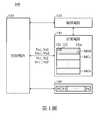
第1圖為本發明之電阻式記憶體的一可能實施例。Figure 1 is a possible embodiment of the resistive memory of the present invention.
第2圖為本發明之電阻式記憶體的設置方法的流程示意圖。FIG. 2 is a schematic flow chart of the method for installing a resistive memory of the present invention.
第3圖為本發明之電阻式記憶體的設置方法的另一流程示意圖。FIG. 3 is another schematic flow chart of the method for installing a resistive memory of the present invention.
第4圖為本發明之電阻式記憶體的重置方法的流程示意圖。FIG. 4 is a schematic flowchart of the reset method of the resistive memory of the present invention.
為讓本發明之目的、特徵和優點能更明顯易懂,下文特舉出實施例,並配合所附圖式,做詳細之說明。本發明說明書提供不同的實施例來說明本發明不同實施方式的技術特徵。其中,實施例中的各元件之配置係為說明之用,並非用以限制本發明。另外,在本發明所指的電壓大小係指所述電壓的脈衝在強度、振幅、或寬度的大小。舉例而言,當敘述第一電壓在實質上大於第二電壓時,係指第一電壓的電壓脈衝可在強度、振幅、或寬度上大於第二電壓。In order to make the purpose, features and advantages of the present invention more comprehensible, the following examples are given in detail and described in detail in conjunction with the accompanying drawings. The description of the present invention provides different examples to illustrate the technical features of different embodiments of the present invention. Among them, the configuration of each element in the embodiment is for illustrative purposes, and is not intended to limit the present invention. In addition, the magnitude of the voltage referred to in the present invention refers to the magnitude of the intensity, amplitude, or width of the pulse of the voltage. For example, when it is stated that the first voltage is substantially greater than the second voltage, it means that the voltage pulse of the first voltage may be greater than the second voltage in intensity, amplitude, or width.
第1圖為本發明之電阻式記憶體的一可能實施例。如圖所示,電阻式記憶體100包括一控制電路110、驗證電路120以及記憶電路130及140。記憶電路130具有記憶胞組MG0~MGn。記憶胞組MG0~MGn構成一記憶陣列(memory array)。在一實施例中,記憶胞組MG0~MGn之每一者具有多個記憶胞131~13m(memory cell),且每一記憶胞組可具有相同數量的記憶胞。舉例而言,記憶胞組MG0~MGn之每一者可各具有32個記憶胞,但本發明不限於此,記憶胞組MG0~MGn之每一者也可具有更多或更少的記憶胞。在另一實施例中,每一記憶胞組可各自具有不同數量的記憶胞。舉例而言,記憶胞組MG0可具有4個記憶胞,記憶胞組MG1可具有8個記憶胞,記憶胞組MG2可具有16個記憶胞......等,以此類推。Figure 1 is a possible embodiment of the resistive memory of the present invention. As shown, the
記憶電路140儲存旗標位元(flag bit)F0~Fn。旗標位元F0~Fn分別對應記憶胞組MG0~MGn。舉例而言,旗標位元F0對應記憶胞組MG0,旗標位元F1對應記憶胞組MG1,旗標位元Fn對應記憶胞組MGn,以此類推。旗標位元F0~Fn之每一者具有一第一旗標狀態或一第二旗標狀態。以旗標位元F0為例,當旗標位元F0為第一數值(如0或1)時,表示旗標位元F0具有第一旗標狀態。當旗標位元F0為第二數值(如1或0)時,表示旗標位元F0具有第二旗標狀態。在一實施例中,旗標位元F0~Fn的初始狀態為第一旗標狀態。在此是以旗標位元具有兩種旗標狀態為例進行說明,但本發明不限於此,本領域人員亦可根據不同的設計使旗標位元具有多種旗標狀態。The
驗證電路120耦接至記憶電路130,用以執行一驗證步驟。該驗證步驟係判斷對記憶電路130中的記憶胞進行的一特定操作是否成功,並將判斷結果提供給控制電路110。舉例而言,在一實施例中,當對記憶電路130中的一記憶胞進行一特定操作時,驗證電路120可根據流經該記憶胞的電流與一預設的驗證電流的比較結果,判斷對該記憶胞所進行的特定操作是否成功。在另一實施例中,當對記憶電路130中的一記憶胞組進行一特定操作時,驗證電路120可逐一將流經該記憶胞組中所有記憶胞的電流與一預設的驗證電流的比較,並根據比較結果判斷對該記憶胞組進行的特定操作是否成功。本發明並不限定驗證電路120如何讀取流經記憶電路130中的記憶胞的電流。在一可能實施例中,驗證電路120先提供一電流予記憶電路130的一特定記憶胞,再讀取流經該記憶胞的電流,並將讀取結果與預設的驗證電流進行比較。The
控制電路110耦接驗證電路120、記憶電路130以及記憶電路140。在本實施例中,控制電路110根據驗證電路120的判斷結果,施加適當的電壓,例如設置電壓(如Vs1或Vs2)、反相設置電壓(如Vis1或Vis2)、或重置電壓(如Vr1、Vr1’、Vr2、或Vr2’)予記憶電路130。在本實施例中,控制電路110更根據驗證電路120的判斷結果,調整旗標位元F0~Fn的旗標狀態。The
在一設置期間(set period),控制電路110對記憶陣列130中的一記憶胞(例如記憶胞131)進行一設置操作(set operation),並透過驗證電路120判斷該記憶胞是否設置成功。若是,控制電路110結束設置操作。若否,控制電路110可能繼續進行設置操作的其他步驟並判斷對該記憶胞進行的設置操作是否成功,或者判定對該記憶胞進行的設置操作失敗並結束設置操作。During a set period, the
特別說明的是,本發明的設置操作至少包括一施加設置電壓(例如Vs1或Vs2)的步驟、一施加反相設置電壓(例如Vis1或Vis2)的步驟以及在每次施加電壓後判斷設置操作是否成功的多個驗證步驟。以設置電壓Vs1與反相設置電壓Vis1為例,設置電壓Vs1與反相設置電壓Vis1的相位相反,且設置電壓Vs1大小的絕對值大於反相設置電壓Vis1大小的絕對值。在一實施例中,施加設置電壓Vs1的步驟例如是通過對耦接至記憶胞(例如記憶胞131)的字元線施加一閘極電壓、對耦接至記憶胞的位元線施加設置電壓Vs1,並將耦接至記憶胞的源極線接地進行。另外,施加反相設置電壓Vis1的步驟例如是通過對耦接至記憶胞(例如記憶胞131)的字元線施加一閘極電壓、對耦接至記憶胞的源極線施加反相設置電壓Vis1,並將耦接至記憶胞的位元線接地進行。In particular, the setting operation of the present invention includes at least a step of applying a setting voltage (such as Vs1 or Vs2), a step of applying a reverse setting voltage (such as Vis1 or Vis2), and determining whether the setting operation is performed after each voltage is applied Multiple successful verification steps. Taking the setting voltage Vs1 and the reverse setting voltage Vis1 as an example, the setting voltage Vs1 and the reverse setting voltage Vis1 have opposite phases, and the absolute value of the setting voltage Vs1 is greater than the absolute value of the inverse setting voltage Vis1. In one embodiment, the step of applying the set voltage Vs1 is, for example, by applying a gate voltage to the word line coupled to the memory cell (eg, memory cell 131) and applying the set voltage to the bit line coupled to the memory cell Vs1, and ground the source line coupled to the memory cell. In addition, the step of applying the reverse setting voltage Vis1 is, for example, by applying a gate voltage to the word line coupled to the memory cell (e.g., memory cell 131).The source line connected to the memory cell is applied with the reverse setting voltage Vis1, and the bit line coupled to the memory cell is grounded.
值得注意的是,本發明的施加反相設置電壓(例如Vis1或Vis2)的步驟是在施加設置電壓(例如Vs1或Vs2)後的驗證步驟判斷出設置操作不成功後才進行的。其中,需進一步說明的是,因應電阻式記憶體在執行上述施加設置電壓的步驟後,有一定數量的氧離子可能卡在記憶胞的傳導燈絲(conducting filament)與上電極的連接面上,使得在施加設置電壓的步驟後,流經記憶胞的電流仍無法達一目標值,導致設置操作不成功。因此,本發明會在施加設置電壓後的驗證步驟判斷出設置操作不成功時,執行施加反相設置電壓的步驟。此處,施加反相設置電壓的步驟係用以推開卡在連接面上的氧離子,使得流經記憶胞的電流可以有效增加。然而,如果在施加反相設置電壓後,仍發現無法使流經記憶胞的電流有效增加,則代表記憶胞開始出現劣化的傾向。It is worth noting that the step of applying the reverse setting voltage (such as Vis1 or Vis2) of the present invention is performed after the verification step after applying the setting voltage (such as Vs1 or Vs2) determines that the setting operation is unsuccessful. Among them, it should be further explained that, after the resistive memory performs the step of applying the setting voltage, a certain amount of oxygen ions may be stuck on the connection surface of the conducting filament of the memory cell and the upper electrode, so that After the step of applying the setting voltage, the current flowing through the memory cell still cannot reach a target value, resulting in an unsuccessful setting operation. Therefore, in the present invention, when the verification step after applying the setting voltage determines that the setting operation is unsuccessful, the step of applying the inverted setting voltage is performed. Here, the step of applying the reverse setting voltage is to push away the oxygen ions stuck on the connection surface, so that the current flowing through the memory cell can be effectively increased. However, if after applying the reverse setting voltage, it is still found that the current flowing through the memory cell cannot be effectively increased, it means that the memory cell starts to deteriorate.
在本發明的一實施例中,若對記憶胞(例如記憶胞131)進行設置操作,並在施加反相設置電壓後的驗證步驟前,成功地設置記憶胞時,則該記憶胞所屬記憶胞組(記憶胞組MG0)對應的旗標位元(旗標位元F0)維持為第一旗標狀態。然而,若對該記憶胞進行設置操作,並在施加反相設置電壓Vis1後的驗證步驟後仍未成功設置該記憶胞時,則控制電路110會將該記憶胞所屬記憶胞組對應的旗標位元(旗標位元F0)調整為第二旗標狀態。在本發明的另一實施例中,當設置操作包括多個施加反相設置電壓Vis的步驟時,控制電路110可以根據設計需求選擇性地在任一施加反相設置電壓(例如Vis1或Vis2)後的驗證步驟判斷出仍未成功設置該記憶胞時,才將對應的旗標位元調整為第二旗標狀態。In an embodiment of the present invention, if a memory cell (eg, memory cell 131) is set and the memory cell is successfully set before the verification step after applying the reverse setting voltage, the memory cell to which the memory cell belongs The flag bit (flag bit F0) corresponding to the group (memory cell group MG0) remains in the first flag state. However, if a setting operation is performed on the memory cell and the memory cell is not successfully set after the verification step after applying the reverse setting voltage Vis1, the
在一重置期間,控制電路110根據一記憶胞(例如記憶胞132)所屬記憶胞組(記憶胞組MG0)對應的旗標位元(旗標位元F0),對該記憶胞進行不同的重置操作(reset operation),並透過驗證電路120,判斷對該記憶胞的重置操作是否成功。若是,控制電路110結束重置操作。若否,控制電路110可能繼續進行重置操作的其他步驟並判斷對該記憶胞的重置操作是否成功,或者判定對該記憶胞的重置操作失敗並結束重置操作。During a reset period, the
在本發明的一實施例中,當旗標位元具有第一旗標狀態時,控制電路110輸出一正常的重置電壓(例如Vr1),用以對該記憶胞進行一第一重置操作。當旗標位元具有第二旗標狀態時,表示此時記憶胞已開始出現劣化的傾向,因此,控制電路110輸出較弱的重置電壓(例如Vr1’),用以對記憶胞進行一第二重置操作,避免記憶胞加速劣化。In an embodiment of the invention, when the flag bit has the first flag state, the
特別說明的是,本發明的重置操作至少包括一施加重置電壓(例如Vr1)的步驟以及在每次施加電壓後判斷重置操作是否成功的至少一驗證步驟。以重置電壓Vr1為例,重置電壓Vr1與反相設置電壓Vis1的相位相同,且重置電壓Vr1大小的絕對值大於反相設置電壓Vis1大小的絕對值。在一實施例中,重置電壓Vr1的大小介於反相設置電壓Vis1的4/3~2倍之間。在一實施例中,施加重置電壓Vr1的步驟例如是通過對耦接至記憶胞(例如記憶胞132)的字元線施加閘極電壓,對耦接至記憶胞的源極線施加重置電壓,並將耦接至記憶胞的位元線接地進行。In particular, the reset operation of the present invention includes at least a step of applying a reset voltage (for example, Vr1) and at least one verification step of determining whether the reset operation is successful after each voltage application. Taking the reset voltage Vr1 as an example, the reset voltage Vr1 has the same phase as the reverse setting voltage Vis1, and the absolute value of the reset voltage Vr1 is greater than the absolute value of the reverse setting voltage Vis1. In one embodiment, the magnitude of the reset voltage Vr1 is between 4/3 and 2 times the reverse setting voltage Vis1. In one embodiment, the step of applying the reset voltage Vr1 is, for example, by coupling theA gate voltage is applied to a word line of a memory cell (for example, memory cell 132), a reset voltage is applied to a source line coupled to the memory cell, and a bit line coupled to the memory cell is grounded.
第2圖為本發明之電阻式記憶體的設置方法的流程示意圖。假設,控制電路110係對記憶胞131進行一設置操作。首先,控制電路110對記憶胞131施加一設置電壓Vs1(步驟S211)。在一實施例中,設置電壓Vs1為一正電壓。FIG. 2 is a schematic flow chart of the method for installing a resistive memory of the present invention. Suppose that the
接著,驗證電路120執行一驗證步驟,以判斷設置操作是否成功(步驟S212),並將判斷結果提供給控制電路110。在本實施例的驗證步驟中,驗證電路120可通過比較流經記憶胞131的電流是否大於等於一預設的驗證電流Ivfy1以判斷設置操作是否成功。亦即,當流經記憶胞131的電流大於等於驗證電流Ivfy1時,表示設置操作成功。相反地,當流經記憶胞131的電流小於驗證電流Ivfy1時,表示設置操作不成功,此時,控制電路110可能繼續進行設置操作的下一步驟或判定設置操作失敗而結束設置操作。Next, the
當判斷出設置操作成功時,控制電路110結束設置操作(步驟S221)。然而,當判斷出設置操作不成功時,控制電路110對記憶體131施加一反相設置電壓Vis1(步驟S213)。在一實施例中,反相設置電壓Vis1係為一負電壓。在另一實施例中,反相設置電壓Vis1的絕對值小於設置電壓Vs1的絕對值。When it is determined that the setting operation is successful, the
接著,驗證電路120再次執行驗證步驟以判斷設置操作是否成功(步驟S214),並將判斷結果提供給控制電路110。當判斷出設置操作成功時,控制電路110結束設置操作(步驟S221)。然而,當驗證電路120再次判斷出設置操作不成功時,控制電路110則將記憶胞131所屬記憶胞組MG0對應的旗標位元F0設定為第二旗標狀態(步驟S219)。此時,由於記憶胞131可能已經發生故障,因此控制電路110判定設置操作失敗並結束設置操作(步驟S220)。Next, the
在一些實施例中,在執行步驟S219時,控制電路110亦可繼續執行設置操作的其他步驟並持續判斷設置操作是否成功,直到設置操作中預設的所有步驟都執行完後,仍未判斷出設置操作成功時,才執行步驟S220。In some embodiments, when step S219 is performed, the
在此說明的是,當步驟S213對記憶胞131施加的反相設置電壓Vis1未能使對記憶胞131的設置操作成功時(即步驟S214判斷出設置操作不成功),表示記憶胞131及所屬記憶胞組MG0的其他記憶胞132~13m可能已經出現劣化的傾向,因此本發明在步驟S219時會將記憶胞131所屬記憶胞組MG0對應的旗標位元F0設定為第二旗標狀態。It is explained here that when the reverse setting voltage Vis1 applied to the
第3圖繪示本發明之電阻式記憶體的設置方法的另一流程示意圖。第3圖相似第2圖,不同之處在於第3圖多了步驟S315~S318。其中,由於第3圖的步驟S311~S314相同於第2圖的步驟S211~S214,且步驟S319~S321相同於第2圖的步驟S219~S221,故不再贅述。FIG. 3 is another schematic flow chart of the method for installing a resistive memory of the present invention. Figure 3 is similar to Figure 2 except that Figure 3 has additional steps S315-S318. Among them, since steps S311 to S314 in FIG. 3 are the same as steps S211 to S214 in FIG. 2, and steps S319 to S321 are the same as steps S219 to S221 in FIG. 2, they will not be repeated here.
請參照第3圖,在步驟S315中,當步驟S314判斷出設置操作不成功時,控制電路110對記憶胞131施加設置電壓Vs2。在一實施例中,設置電壓Vs2係為一正電壓。在一實施例中,設置電壓Vs2的大小可能相同或大於設置電壓Vs1。Referring to FIG. 3, in step S315, when it is determined in step S314 that the setting operation is unsuccessful, the
接著,驗證電路120執行驗證步驟以判斷設置操作是否成功(步驟S316),並將判斷結果提供給控制電路110。當判斷出設置操作成功時,控制電路110結束設置操作(步驟S321)。當判斷出設置操作不成功時,控制電路110對記憶胞131施加一反相設置電壓Vis2(步驟S317)。在本實施例中,反相設置電壓Vis2係為一負電壓。且反相設置電壓Vis2大小的絕對值在實質上可能相同或大於反相設置電壓Vis1。Next, the
之後,驗證電路120再次執行驗證步驟以判斷設置操作是否成功(步驟S318)。當判斷出設置操作成功時,結束設置操作(步驟S321)。然而,當判斷出設置操作不成功時,控制電路11則將旗標位元F0設定為第二旗標狀態(步驟S319),並判定設置操作失敗而結束設置操作(步驟S320)。After that, the
在此特別說明的是,在一些實施例中,當如第3圖的實施例所示,若電阻式記憶體的設置方法包含了多個施加反相設置電壓的步驟(如步驟S313及S317)時,使用者可根據需求(例如產品設計、製程能力)的不同,選擇性地在任一施加反相設置電壓後的驗證步驟(如步驟S314及S318)後判斷出仍未成功設置該記憶胞時,將對應的旗標位元調整為第二旗標狀態。It is particularly explained here that in some embodiments, as shown in the embodiment of FIG. 3, if the setting method of the resistive memory includes multiple steps of applying an inverse setting voltage (such as steps S313 and S317) At this time, the user can selectively determine whether the memory cell has not been successfully set after any verification step (such as steps S314 and S318) after applying the reverse setting voltage according to different needs (eg product design, process capability) , Adjust the corresponding flag bit to the second flag state.
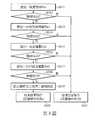
第4圖為本發明之電阻式記憶體的重置方法的一流程示意圖。在本實施例中,控制電路110係根據旗標位元F0~Fn,對記憶胞執行一第一重置操作或一第二重置操作。為清楚說明本發明的重置方法,在此假設控制電路110係對記憶陣列130的另一記憶胞132執行重置操作。FIG. 4 is a schematic flow chart of the reset method of the resistive memory of the present invention. In this embodiment, the
首先,控制電路110判斷記憶胞132所屬記憶胞組MG0所對應的旗標位元F0的旗標狀態(步驟S410)。當旗標位元F0具有第一旗標狀態時,表示記憶胞組MG0中的記憶胞131~13m尚未出現劣化的傾向。因此,控制電路110對記憶胞132執行第一重置操作S420。第一重置操作S420包括步驟S421~S425及S440。First, the
在步驟S421中,控制電路110對記憶胞132施加一重置電壓Vr1。在一實施例中,重置電壓Vr1係為一負電壓。在另一實施例中,重置電壓Vr1的大小的絕對值大於反相設置電壓Vis1及Vis2的大小的絕對值。在其他實施例中,重置電壓Vr1的大小介於反相設置電壓Vis1及Vis2的4/3~2倍之間。In step S421, the
接著,驗證電路120執行一驗證步驟以判斷重置操作是否成功(步驟S422),並將判斷結果提供給控制電路110。在本實施例的驗證步驟中,驗證電路120可通過比較流經記憶胞132的電流是否小於等於一預設的驗證電流Ivfy2以判斷重置操作是否成功。亦即,當流經記憶胞132的電流小於等於驗證電流Ivfy2時,表示重置操作成功。相反地,當流經記憶胞132的電流大於驗證電流Ivfy2時,表示重置操作不成功,此時,控制電路110可能繼續進行重置操作的下一步驟或判定重置操作失敗而結束重置操作。Next, the
當判斷出重置操作成功時,控制電路110結束重置操作(步驟S440)。然而,當判斷出重置操作不成功時,控制電路110對記憶胞132施加重置電壓Vr2(步驟S423)。在一實施例中,重置電壓Vr2為一負電壓。在另一實施例中,重置電壓Vr2的絕對值在實質上大於或等於重置電壓Vr1的絕對值。When it is determined that the reset operation is successful, the
之後,驗證電路120再次執行驗證步驟以判斷重置操作是否成功(步驟S424),並將判斷結果提供給控制電路110。當判斷出重置操作成功時,控制電路110結束重置操作(步驟S440)。然而,當再次判斷出重置操作不成功時,表示記憶胞132無法被重置。因此,控制電路110判定重置操作失敗並結束第一重置操作(步驟S425)。After that, the
請回到步驟S410,當旗標位元F0具有第二旗標狀態時,表示記憶胞組MG0中的記憶胞131~13m可能已經出現劣化的傾向。因此,控制電路110對記憶胞132執行第二重置操作S430。第二重置操作S430包括步驟S431~S435及S440。Please return to step S410. When the flag bit F0 has the second flag state, it indicates that the
在步驟S431中,控制電路110對記憶胞132施加一重置電壓Vr1’。在一實施例中,重置電壓Vr1’係為一負電壓。重置電壓Vr1’的大小在實質上小於重置電壓Vr1。In step S431, the
接著,驗證電路120執行驗證步驟以判斷重置操作是否成功(步驟S432),並將判斷結果提供給控制電路110。當判斷出重置操作成功時,控制電路110結束重置操作(步驟S440)。然而,當判斷出重置操作不成功時,控制電路110對記憶胞132施加一重置電壓Vr2’(步驟S433)。在一實施例中,重置電壓Vr2’係為一負電壓。重置電壓Vr2’的大小在實質上可能大於或等於重置電壓Vr1’。Next, the
接著,驗證電路120再次執行驗證步驟以判斷重置操作是否成功(步驟S434),並將判斷結果提供給控制電路110。當判斷出重置操作成功時,控制電路110結束重置操作(步驟S440)。然而,當再次判斷出重置操作不成功時,表示記憶胞132無法被重置,故控制電路110結束第二重置操作(步驟S435)。Next, the
在本發明中,由於當記憶胞組中的任一記憶胞出現劣化的現象時,控制電路會變更該記憶胞所屬記憶胞組的旗標位元的旗標狀態。並且,本發明會根據旗標位元的不同旗標狀態,對正常記憶胞組中的記憶胞使用正常的重置電壓進行重置操作,並對劣化的記憶胞組中的記憶胞使用較弱的重置電壓進行重置操作,故可增加電阻式記憶體的耐受力(endurance)、可靠度(reliability)及性能。再者,由於本發明不需計數電阻式記憶體中的記憶胞的操作次數以判斷記憶胞是否可能會開始劣化,故可減少電阻式記憶體的功耗,並增加電阻式記憶體的可使用空間。In the present invention, when any memory cell in the memory cell group deteriorates, the control circuit changes the flag state of the flag bit of the memory cell group to which the memory cell belongs. In addition, according to different flag states of the flag bits, the present invention performs a reset operation on the memory cells in the normal memory cell group using a normal reset voltage, and uses weaker memory cells in the deteriorated memory cell group The reset voltage is reset, so the endurance, reliability and performance of the resistive memory can be increased. Furthermore, since the present invention does not need to count the number of operations of the memory cell in the resistive memory to determine whether the memory cell may start to deteriorate, it can reduce the power consumption of the resistive memory and increase the usability of the resistive memory space.
除非另作定義,在此所有詞彙(包含技術與科學詞彙)均屬本發明所屬技術領域中具有通常知識者之一般理解。此外,除非明白表示,詞彙於一般字典中之定義應解釋為與其相關技術領域之文章中意義一致,而不應解釋為理想狀態或過分正式之語態。Unless otherwise defined, all vocabulary (including technical and scientific vocabulary) herein belongs to the general understanding of those with ordinary knowledge in the technical field to which the present invention belongs. In addition, unless clearly stated, the definition of vocabulary in a general dictionary should be interpreted to be consistent with the meaning in articles in the related technical field, and should not be interpreted as an ideal state or an excessively formal voice.
雖然本發明已以較佳實施例揭露如上,然其並非用以限定本發明,任何所屬技術領域中具有通常知識者,在不脫離本發明之精神和範圍內,當可作些許之更動與潤飾。舉例來,本發明實施例所系統、裝置或是方法可以硬體、軟體或硬體以及軟體的組合的實體實施例加以實現。因此本發明之保護範圍當視後附之申請專利範圍所界定者為準。Although the present invention has been disclosed as above with preferred embodiments, it is not intended to limit the present invention. Any person with ordinary knowledge in the technical field can make some changes and modifications without departing from the spirit and scope of the present invention. . For example, the system, device, or method in the embodiments of the present invention may be implemented by physical embodiments of hardware, software, or a combination of hardware and software. Therefore, the protection scope of the present invention shall be subject to the scope defined in the appended patent application.
S410、S420~S425、S430~S435、S440‧‧‧步驟S410, S420~S425, S430~S435, S440
Claims (16)
Translated fromChinesePriority Applications (1)
| Application Number | Priority Date | Filing Date | Title |
|---|---|---|---|
| TW108100845ATWI689929B (en) | 2019-01-09 | 2019-01-09 | Resistive memory and control method |
Applications Claiming Priority (1)
| Application Number | Priority Date | Filing Date | Title |
|---|---|---|---|
| TW108100845ATWI689929B (en) | 2019-01-09 | 2019-01-09 | Resistive memory and control method |
Publications (2)
| Publication Number | Publication Date |
|---|---|
| TWI689929Btrue TWI689929B (en) | 2020-04-01 |
| TW202027081A TW202027081A (en) | 2020-07-16 |
Family
ID=71132522
Family Applications (1)
| Application Number | Title | Priority Date | Filing Date |
|---|---|---|---|
| TW108100845ATWI689929B (en) | 2019-01-09 | 2019-01-09 | Resistive memory and control method |
Country Status (1)
| Country | Link |
|---|---|
| TW (1) | TWI689929B (en) |
Citations (4)
| Publication number | Priority date | Publication date | Assignee | Title |
|---|---|---|---|---|
| US7969806B2 (en)* | 2008-04-28 | 2011-06-28 | Qimonda Ag | Systems and methods for writing to a memory |
| US10067683B2 (en)* | 2016-07-19 | 2018-09-04 | Western Digital Technologies, Inc. | Systems and methods for classifying data in solid state drives |
| TWI637393B (en)* | 2016-12-08 | 2018-10-01 | 華邦電子股份有限公司 | Semiconductor device and adjusting method thereof |
| US20180366187A1 (en)* | 2015-01-14 | 2018-12-20 | Industrial Technology Research Institute | Method for controlling resistive random-access memory |
- 2019
- 2019-01-09TWTW108100845Apatent/TWI689929B/enactive
Patent Citations (4)
| Publication number | Priority date | Publication date | Assignee | Title |
|---|---|---|---|---|
| US7969806B2 (en)* | 2008-04-28 | 2011-06-28 | Qimonda Ag | Systems and methods for writing to a memory |
| US20180366187A1 (en)* | 2015-01-14 | 2018-12-20 | Industrial Technology Research Institute | Method for controlling resistive random-access memory |
| US10067683B2 (en)* | 2016-07-19 | 2018-09-04 | Western Digital Technologies, Inc. | Systems and methods for classifying data in solid state drives |
| TWI637393B (en)* | 2016-12-08 | 2018-10-01 | 華邦電子股份有限公司 | Semiconductor device and adjusting method thereof |
Also Published As
| Publication number | Publication date |
|---|---|
| TW202027081A (en) | 2020-07-16 |
Similar Documents
| Publication | Publication Date | Title |
|---|---|---|
| US8254181B2 (en) | Nonvolatile memory device and programming method | |
| US8228731B2 (en) | Random access memory with CMOS-compatible nonvolatile storage element and parallel storage capacitor | |
| JP5413697B2 (en) | Method, apparatus, and system for coping with changes in threshold voltage in memory device | |
| US9858993B2 (en) | Non-volatile memory device and method of programming the same | |
| TWI363345B (en) | Erase algorithm for multi-level bit flash memory | |
| US20140237165A1 (en) | Memory controller, method of operating the same and memory system including the same | |
| US11984164B2 (en) | Non-volatile static random access memory (nvSRAM) with multiple magnetic tunnel junction cells | |
| EP1652191A1 (en) | Detecting over programmed memory cells after programming of adjacent memory cells | |
| KR20090124100A (en) | Nonvolatile Memory Device and Operation Method | |
| JP7236788B2 (en) | Counter-based reads in memory devices | |
| TW201320086A (en) | Determining and transferring data from a memory array | |
| US20090285020A1 (en) | Method of programming a multi level cell in a non-volatile memory device | |
| CN107045888B (en) | Data erasing method | |
| TW201232546A (en) | Non-volatile memory device and cache program method of the same | |
| JP6405612B2 (en) | Ferroelectric memory device and memory writing method | |
| US20090237997A1 (en) | Random access memory with cmos-compatible nonvolatile storage element | |
| US11742034B2 (en) | Memory device including dynamic programming voltage | |
| CN100570749C (en) | Method for judging logic state of storage unit of flash memory | |
| TWI689929B (en) | Resistive memory and control method | |
| CN101169973A (en) | High programming speed multi-level cell memory | |
| US20170162269A1 (en) | Apparatuses and methods for reducing read disturb | |
| TW201705149A (en) | Semiconductor memory device | |
| KR100703806B1 (en) | Non-volatile memory, apparatus and method for determining data validity therefor | |
| CN111554337B (en) | Resistive memory and control method | |
| CN107430889B (en) | Rewriting method of semiconductor storage device and semiconductor storage device |