TWI688127B - Packaging method for semiconductor light emitting module - Google Patents
Packaging method for semiconductor light emitting moduleDownload PDFInfo
- Publication number
- TWI688127B TWI688127BTW108108944ATW108108944ATWI688127BTW I688127 BTWI688127 BTW I688127BTW 108108944 ATW108108944 ATW 108108944ATW 108108944 ATW108108944 ATW 108108944ATW I688127 BTWI688127 BTW I688127B
- Authority
- TW
- Taiwan
- Prior art keywords
- light emitting
- semiconductor light
- emitting module
- packaging
- opening
- Prior art date
Links
- 238000004806packaging method and processMethods0.000titleclaimsabstractdescription24
- 239000004065semiconductorSubstances0.000titleclaimsabstractdescription23
- 238000000034methodMethods0.000titleclaimsabstractdescription22
- 238000002347injectionMethods0.000claimsabstractdescription39
- 239000007924injectionSubstances0.000claimsabstractdescription39
- 239000000758substrateSubstances0.000claimsabstractdescription24
- 229910000679solderInorganic materials0.000claimsabstractdescription20
- 239000008393encapsulating agentSubstances0.000claimsabstractdescription14
- 239000000463materialSubstances0.000claimsabstractdescription7
- 239000000919ceramicSubstances0.000claimsabstractdescription6
- 239000003292glueSubstances0.000claimsdescription25
- 239000000084colloidal systemSubstances0.000claimsdescription18
- 238000009792diffusion processMethods0.000claimsdescription6
- 239000002245particleSubstances0.000claimsdescription6
- 239000004593EpoxySubstances0.000claimsdescription4
- 238000003848UV Light-CuringMethods0.000claimsdescription4
- NIXOWILDQLNWCW-UHFFFAOYSA-Nacrylic acid groupChemical groupC(C=C)(=O)ONIXOWILDQLNWCW-UHFFFAOYSA-N0.000claimsdescription4
- 239000002184metalSubstances0.000claimsdescription4
- 229910052751metalInorganic materials0.000claimsdescription4
- 229920001296polysiloxanePolymers0.000claimsdescription4
- 229910018072Al 2 O 3Inorganic materials0.000claimsdescription3
- 229910004298SiO 2Inorganic materials0.000claimsdescription3
- 229910010413TiO 2Inorganic materials0.000claimsdescription3
- 238000004026adhesive bondingMethods0.000claims3
- 239000007787solidSubstances0.000claims3
- 238000005516engineering processMethods0.000description5
- CNQCVBJFEGMYDW-UHFFFAOYSA-Nlawrencium atomChemical compound[Lr]CNQCVBJFEGMYDW-UHFFFAOYSA-N0.000description4
- 238000000465mouldingMethods0.000description2
- 238000012858packaging processMethods0.000description2
- 239000011347resinSubstances0.000description2
- 229920005989resinPolymers0.000description2
- RYGMFSIKBFXOCR-UHFFFAOYSA-NCopperChemical compound[Cu]RYGMFSIKBFXOCR-UHFFFAOYSA-N0.000description1
- 229910052802copperInorganic materials0.000description1
- 239000010949copperSubstances0.000description1
- 238000010586diagramMethods0.000description1
- 239000007788liquidSubstances0.000description1
- 238000007789sealingMethods0.000description1
- 238000005476solderingMethods0.000description1
Images


Classifications
- H—ELECTRICITY
- H10—SEMICONDUCTOR DEVICES; ELECTRIC SOLID-STATE DEVICES NOT OTHERWISE PROVIDED FOR
- H10H—INORGANIC LIGHT-EMITTING SEMICONDUCTOR DEVICES HAVING POTENTIAL BARRIERS
- H10H20/00—Individual inorganic light-emitting semiconductor devices having potential barriers, e.g. light-emitting diodes [LED]
- H10H20/01—Manufacture or treatment
- H—ELECTRICITY
- H10—SEMICONDUCTOR DEVICES; ELECTRIC SOLID-STATE DEVICES NOT OTHERWISE PROVIDED FOR
- H10H—INORGANIC LIGHT-EMITTING SEMICONDUCTOR DEVICES HAVING POTENTIAL BARRIERS
- H10H20/00—Individual inorganic light-emitting semiconductor devices having potential barriers, e.g. light-emitting diodes [LED]
- H10H20/80—Constructional details
- H10H20/85—Packages
- H10H20/852—Encapsulations
- H10H20/854—Encapsulations characterised by their material, e.g. epoxy or silicone resins
- H—ELECTRICITY
- H10—SEMICONDUCTOR DEVICES; ELECTRIC SOLID-STATE DEVICES NOT OTHERWISE PROVIDED FOR
- H10H—INORGANIC LIGHT-EMITTING SEMICONDUCTOR DEVICES HAVING POTENTIAL BARRIERS
- H10H20/00—Individual inorganic light-emitting semiconductor devices having potential barriers, e.g. light-emitting diodes [LED]
- H10H20/80—Constructional details
- H10H20/85—Packages
- H10H20/857—Interconnections, e.g. lead-frames, bond wires or solder balls
- H—ELECTRICITY
- H10—SEMICONDUCTOR DEVICES; ELECTRIC SOLID-STATE DEVICES NOT OTHERWISE PROVIDED FOR
- H10H—INORGANIC LIGHT-EMITTING SEMICONDUCTOR DEVICES HAVING POTENTIAL BARRIERS
- H10H20/00—Individual inorganic light-emitting semiconductor devices having potential barriers, e.g. light-emitting diodes [LED]
- H10H20/01—Manufacture or treatment
- H10H20/036—Manufacture or treatment of packages
- H10H20/0362—Manufacture or treatment of packages of encapsulations
- H—ELECTRICITY
- H10—SEMICONDUCTOR DEVICES; ELECTRIC SOLID-STATE DEVICES NOT OTHERWISE PROVIDED FOR
- H10H—INORGANIC LIGHT-EMITTING SEMICONDUCTOR DEVICES HAVING POTENTIAL BARRIERS
- H10H20/00—Individual inorganic light-emitting semiconductor devices having potential barriers, e.g. light-emitting diodes [LED]
- H10H20/80—Constructional details
- H10H20/85—Packages
- H10H20/852—Encapsulations
- H10H20/853—Encapsulations characterised by their shape
Landscapes
- Led Device Packages (AREA)
Abstract
Description
Translated fromChinese本發明係有關於一種電子元件封裝的應用領域,尤指一種半導體發光模組的封裝方法。The invention relates to an application field of electronic component packaging, in particular to a packaging method of a semiconductor light emitting module.
隨著電子產品的小型化趨勢,電路板也需製作地更加輕薄,使得電路板上的導電線路及連接端子的排列也越來越密集且複雜,而發光元件的尺寸也愈來愈小。相應地,在組裝過程中,對所述發光元件之組裝精度的要求也越來越高。With the trend of miniaturization of electronic products, circuit boards also need to be made lighter and thinner, which makes the arrangement of conductive circuits and connection terminals on the circuit boards more and more dense and complicated, and the size of light-emitting elements is getting smaller and smaller. Correspondingly, during the assembly process, the requirements for the assembly accuracy of the light-emitting elements are getting higher and higher.
於現有技術中,通常使利用樹脂模塑技術對基板上所安裝的發光元件,例如:發光二極體晶片進行封裝,以形成覆蓋發光元件的密封透鏡結構,使自發光元件出射之光線可藉由密封透鏡結構進行聚光。In the prior art, resin molding technology is usually used to package the light-emitting elements mounted on the substrate, for example, light-emitting diode chips, to form a sealed lens structure covering the light-emitting elements, so that the light emitted from the light-emitting elements can be borrowed The light is collected by the sealed lens structure.
然而,由於導電線路及連接端子的排列過於密集,也因此提高應用樹脂模塑技術封裝的難度。However, because the arrangement of conductive lines and connection terminals is too dense, it also increases the difficulty of packaging with resin molding technology.
有鑑於此,如何提供一種可簡易且快速的半導體發光模組的封裝方法,同時可形成不同外形及立體高度的密封透鏡結構,為本發明欲解決的技術課題。In view of this, how to provide a simple and fast packaging method of a semiconductor light emitting module, and at the same time can form a sealed lens structure with different shapes and three-dimensional heights, is a technical problem to be solved by the present invention.
本發明之主要目的,在於提供一種可簡易且快速的半導體發光模組的封裝方法,並同時形成不同外形及立體高度的密封透鏡結構,以藉此調整發光元件的聚光度。The main object of the present invention is to provide a simple and fast packaging method of a semiconductor light emitting module, and at the same time form a sealed lens structure with different shapes and three-dimensional heights, thereby adjusting the light concentration of the light emitting element.
為達前述之目的,本發明提供一種半導體發光模組的封裝方法,包括下列步驟:(a).提供基板,基板材質種類可為柔性印刷電路板、金屬印刷電路板、印刷電路板、陶瓷基板;(b.)基板包括防焊層及發光元件,防焊層具有開口且開口具有寬度R,發光元件設置於開口中;(c).藉由注膠裝置將封裝膠體注入開口中;以及(d).形成覆蓋發光元件的密封透鏡結構,密封透鏡結構具有立體高度d。To achieve the foregoing objective, the present invention provides a method for packaging a semiconductor light emitting module, including the following steps: (a) providing a substrate, the substrate material type may be a flexible printed circuit board, a metal printed circuit board, a printed circuit board, a ceramic substrate (B.) The substrate includes a solder mask layer and a light-emitting element, the solder mask layer has an opening and the opening has a width R, the light-emitting element is disposed in the opening; (c). Inject the encapsulating colloid into the opening by the glue injection device; and ( d). A sealed lens structure covering the light-emitting element is formed, and the sealed lens structure has a three-dimensional height d.
於上述較佳實施方式中,其中於步驟(a)中,基板包括電路層,電路層部分暴露於開口中。In the above preferred embodiment, in step (a), the substrate includes a circuit layer, and the circuit layer is partially exposed in the opening.
於上述較佳實施方式中,其中發光元件包括發光二極體晶片及焊墊,焊墊用以電性連接於電路層。In the above-mentioned preferred embodiment, the light-emitting element includes a light-emitting diode chip and a bonding pad, and the bonding pad is used to be electrically connected to the circuit layer.
於上述較佳實施方式中,其中於步驟(c)中,封裝膠體為Epoxy-hybrid,silicone-hybrid,epoxy,silicone,acrylic hybrid,UV curing glue,其封裝膠體可填充擴散粒子,擴散粒子可為CaCO3、TiO2、SiO2、Al2O3、BN、ZnO或ZrO2。。In the above preferred embodiment, in step (c), the encapsulating colloid is Epoxy-hybrid, silicone-hybrid, epoxy, silicone, acrylic hybrid, UV curing glue, the encapsulating colloid can be filled with diffusion particles, and the diffusion particles can be CaCO3 , TiO2 , SiO2 , Al2 O3 , BN, ZnO, or ZrO2 . .
於上述較佳實施方式中,其中於步驟(a)中,寬度R為0.7mm。In the above preferred embodiment, in step (a), the width R is 0.7 mm.
於上述較佳實施方式中,其中於步驟(c)中,注膠裝置的注膠口的口徑介於0.1mm至0.3mm之間。In the above preferred embodiment, in step (c), the diameter of the glue injection port of the glue injection device is between 0.1 mm and 0.3 mm.
於上述較佳實施方式中,其中於步驟(c)中,封裝膠體的黏度介於3000Pa.s至15000Pa.s之間,搖變性介於1.5至6.0之間。In the above preferred embodiment, wherein in step (c), the viscosity of the encapsulating colloid is between 3000Pa. s to 15000Pa. Between s, the shake is between 1.5 and 6.0.
於上述較佳實施方式中,其中注膠裝置的注膠口的口徑介於0.1mm至0.2mm之間,封裝膠體的黏度介於3000Pa.s至8500Pa.s之間,搖變性介於1.5至3.0之間,以形成立體高度d約略等於0.15mm的密封透鏡結構。In the above-mentioned preferred embodiment, the injection port of the injection deviceThe caliber is between 0.1mm and 0.2mm, and the viscosity of the encapsulating colloid is between 3000Pa. s to 8500Pa. Between s, the shake is between 1.5 and 3.0 to form a sealed lens structure with a stereo height d approximately equal to 0.15 mm.
於上述較佳實施方式中,其中注膠裝置的注膠口的口徑介於0.2mm至0.3mm之間,封裝膠體的黏度介於6000Pa.s至15000Pa.s之間,搖變性介於2.4至6.0之間,以形成立體高度d約略等於0.35mm的密封透鏡結構。In the above preferred embodiment, wherein the diameter of the injection port of the injection device is between 0.2mm and 0.3mm, and the viscosity of the encapsulating colloid is between 6000Pa. s to 15000Pa. Between s, the shake is between 2.4 and 6.0 to form a sealed lens structure with a stereo height d approximately equal to 0.35 mm.
於上述較佳實施方式中,其中注膠裝置的注膠口的口徑介於0.2mm至0.3mm之間,封裝膠體的黏度介於3000Pa.s至7000Pa.s之間,搖變性介於1.5至1.9之間,以形成立體高度d約略等於0.15mm的密封透鏡結構。In the above preferred embodiment, wherein the diameter of the injection port of the injection device is between 0.2mm to 0.3mm, the viscosity of the encapsulating colloid is between 3000Pa. s to 7000Pa. Between s, the shake is between 1.5 and 1.9 to form a sealed lens structure with a stereo height d approximately equal to 0.15 mm.
G‧‧‧封裝膠體G‧‧‧encapsulated colloid
N‧‧‧注膠裝置N‧‧‧Glue injection device
NO‧‧‧注膠口NO‧‧‧Glue injection port
R‧‧‧寬度R‧‧‧Width
S101~S104‧‧‧步驟S101~S104‧‧‧Step
10‧‧‧基板10‧‧‧ substrate
10A‧‧‧基板材質10A‧‧‧Substrate material
101‧‧‧防焊層101‧‧‧Soldering layer
1011‧‧‧開口1011‧‧‧ opening
102‧‧‧電路層102‧‧‧ circuit layer
103‧‧‧發光元件103‧‧‧Lighting element
1031‧‧‧發光二極體晶片1031‧‧‧ LED chip
10311‧‧‧出光面10311‧‧‧Light
10312‧‧‧底面10312‧‧‧Bottom
1032‧‧‧焊墊1032‧‧‧solder pad
104、104a、104、104c‧‧‧密封透鏡結構104, 104a, 104, 104c ‧‧‧ sealed lens structure
圖1:係為本發明所提供之半導體發光模組的封裝方法的流程圖;圖2:係為本發明所提供之半導體發光模組的封裝流程示意圖;以及圖3:為本發明所提供半導體發光模組封裝之不同實施例的剖視圖。FIG. 1: is a flowchart of a semiconductor light emitting module packaging method provided by the present invention; FIG. 2: is a schematic flowchart of a semiconductor light emitting module packaging process provided by the present invention; and FIG. 3: a semiconductor provided by the present invention Cross-sectional view of different embodiments of a light emitting module package.
本發明的優點及特徵以及達到其方法將參照例示性實施例及附圖進行更詳細的描述而更容易理解。然而,本發明可以不同形式來實現且不應被理解僅限於此處所陳述的實施例。相反地,對所屬技術領域具有通常知識者而言,所提供的此些實施例將使本揭露更加透徹與全面且完整地傳達本發明的範疇。The advantages and features of the present invention and the methods for achieving it will be described in more detail with reference to the exemplary embodiments and the accompanying drawings to make it easier to understand. However, the present invention can be implemented in different forms and should not be understood as being limited to the embodiments set forth herein. On the contrary, for those of ordinary skill in the art, the provided embodiments will make the disclosure more thorough, comprehensive, and complete to convey the scope of the present invention.
首先,請參閱圖1及圖2所示,圖1係為本發明所提供之半導體發光模組的封裝方法的流程圖;圖2係為本發明所提供之半導體發光模組的封裝流程示意圖。首先,提供基板,基板材質種類可為柔性印刷電路板、金屬印刷電路板、印刷電路板或陶瓷基板(步驟S101),於步驟S101中,基板10的基板材質10A種類可為柔性印刷電路板(FPC)、金屬印刷電路板(MCPCB)、印刷電路板(PCB)或陶瓷基板(Ceramic PCB)。而基板包括防焊層及發光元件,防焊層具有開口且開口具有寬度R,發光元件設置於開口中(步驟S102),於步驟S102中,基板10具有防焊層101,所述防焊層101為一絕緣層,其材料可為:Epoxy-hybrid、silicone-hybrid、epoxy、silicone、acrylic hybrid或UV curing glue。所述防焊層101內則配置有一電路層102,電路層102的材質為銅,並部分暴露於防焊層101的開口1011中,且開口1011具有一寬度R。所述發光元件103以覆晶方法(Flip chip scheme)設置於開口1011中,發光元件103包括發光二極體晶片1031及焊墊1032。發光二極體晶片1031具有一出光面10311及相對於出光面10311的底面10312,焊墊1032則配置於底面10312,而發光二極體晶片1031可藉由焊墊1032電性連接於電路層102,而毋須使用傳統的打線結構。於本實施例中,防焊層101的開口1011係以阻焊層限定(solder mask defined,SMD)技術或非阻焊層限定(non-solder mask defined,NSMD)技術製作,且防焊開窗防焊層101之開口1011的寬度R為為0.7mm。First of all, please refer to FIG. 1 and FIG. 2, FIG. 1A flowchart of a method for packaging a semiconductor light emitting module provided; FIG. 2 is a schematic diagram of a packaging process of a semiconductor light emitting module provided by the present invention. First, a substrate is provided. The substrate material type may be a flexible printed circuit board, a metal printed circuit board, a printed circuit board, or a ceramic substrate (step S101). In step S101, the
接著,藉由注膠裝置將封裝膠體注入開口中(步驟S103),於步驟S103中,注膠裝置N被配置於發光元件103的上方,且注膠裝置N的注膠口NO接近發光二極體晶片1031。如此,便可利用注膠口NO於一預設時間內供給一定量之液狀的封裝膠體G,將封裝膠體G注入開口1011之中以覆蓋發光元件103。於本實施例中,注膠裝置N的注膠口NO之口徑介於0.1mm至0.2mm之間,封裝膠體G可為Epoxy-hybrid、silicone-hybrid、epoxy、silicone、acrylic hybrid或UV curing glue,且封裝膠體G可填充擴散粒子,擴散粒子可為CaCO3、TiO2、SiO2、Al2O3、BN、ZnO、ZrO2。,且其黏度介於3000Pa.s至8500Pa.s之間;搖變性介於1.5至3.0之間。Next, the encapsulant is injected into the opening by the glue injection device (step S103). In step S103, the glue injection device N is disposed above the
最後,形成覆蓋發光元件的密封透鏡結構,密封透鏡結構具有立體高度d(步驟S104),於步驟S104中,可利用調整防焊層101的開口1011的寬度R及封裝膠體G的黏度、搖變性來調整並決定密封透鏡結構104的立體高度d,舉例而言,當開口1011的寬度R越大時,可容納封裝膠體G的體積越大,使得密封透鏡結構104的立體高度d變低,又或者,當封裝膠體G黏度高、搖變性高時,因封裝膠體G的黏性較高則使得密封透鏡結構104的立體高度d變高;當封裝膠體G黏度低、搖變性低時,因封裝膠體G的黏性較低,則會讓密封透鏡結構104的立體高度d變低。Finally, a sealed lens structure covering the light emitting element is formed, and the sealed lens structure has a three-dimensional height d (step S104). In step S104, the width R of the
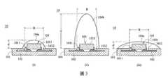
請參閱圖3,圖3為本發明所提供半導體發光模組封裝之不同實施例的剖視圖,當注膠裝置N的注膠口NO的口徑介於0.1mm至0.2mm之間,封裝膠體G的黏度介於3000Pa.s至8500Pa.s之間;搖變性介於1.5至3.0之間時,於預設時間內所注入的封裝膠體G便可形成立體高度d約略等於0.15mm的密封透鏡結構104a(如圖3之(i)所示)。而當注膠裝置N的注膠口NO的口徑介於0.2mm至0.3mm之間,封裝膠體G的黏度介於6000Pa.s至15000Pa.s之間;搖變性介於2.4至6.0之間時,因注膠口NO的口徑較大,使得於預設時間內所注入的封裝膠體G較多,且由於封裝膠體G的黏度較高,因此封裝膠體G便可形成立體高度d約略等於0.35mm的密封透鏡結構104b(如圖3之(ii)所示)。Please refer to FIG. 3, which is a cross-sectional view of different embodiments of a semiconductor light emitting module package provided by the present invention. When the diameter of the glue injection port NO of the glue injection device N is between 0.1mm and 0.2mm, the Viscosity is between 3000Pa. s to 8500Pa. s; when the shake is between 1.5 and 3.0, the encapsulant G injected within the preset time can form a sealed
另一方面,若欲形成覆蓋面積較大的密封透鏡結構時,便可利用口徑較大的注膠口NO注入黏度較低的封裝膠體G,例如:當注膠裝置N的注膠口NO的口徑介於0.2mm至0.3mm之間,封裝膠體的黏度介於3000Pa.s至7000Pa.s之間;搖變性介於1.5至1.9之間時,因注膠口NO的口徑較大,使得於預設時間內所注入的封裝膠體G較多,且封裝膠體G的黏度較低而可向周延擴散,因此封裝膠體G便可以形成立體高度d約略等於0.15mm,且覆蓋面積較大的密封透鏡結構104c(如圖3之(iii)所示)。On the other hand, if you want to form a sealed lens structure with a large coverage area, you can use the larger diameter injection port NO to inject the lower viscosity encapsulant G, for example: when the injection port N of the injection device N The caliber is between 0.2mm and 0.3mm, and the viscosity of the encapsulating colloid is between 3000Pa. s to 7000Pa. s; when the shake is between 1.5 and 1.9, due to the larger diameter of the injection port NO, more encapsulating gel G is injected within the preset time, and the viscosity of the encapsulating gel G is lower and can be Xiang ZhouyanAs a result, the encapsulant G can form a sealed
相較於習知技術,本發明提供一種可簡易且快速的半導體發光模組的封裝方法,並可藉由調整防焊層之開口、注膠裝置之口徑及封裝膠體的黏度、搖變性來調整密封透鏡結構的外型及立體高度,以藉此調整發光元件的聚光度。;故,本發明實為一極具產業價值之創作。Compared with the conventional technology, the present invention provides a simple and fast method for packaging a semiconductor light-emitting module, which can be adjusted by adjusting the opening of the solder mask, the diameter of the glue injection device, and the viscosity and shake of the encapsulant The appearance and three-dimensional height of the sealed lens structure are adjusted to adjust the concentration of the light-emitting element. ; Therefore, the present invention is really a creation of great industrial value.
本發明得由熟悉本技藝之人士任施匠思而為諸般修飾,然皆不脫如附申請專利範圍所欲保護。The present invention may be modified by any person familiar with the art and any craftsmanship, but none of them may be protected as the scope of the attached patent application.
S101~S104‧‧‧步驟S101~S104‧‧‧Step
Claims (10)
Translated fromChinesePriority Applications (2)
| Application Number | Priority Date | Filing Date | Title |
|---|---|---|---|
| TW108108944ATWI688127B (en) | 2019-03-15 | 2019-03-15 | Packaging method for semiconductor light emitting module |
| US16/422,800US10964860B2 (en) | 2019-03-15 | 2019-05-24 | Method of packaging semiconductor illumination module |
Applications Claiming Priority (1)
| Application Number | Priority Date | Filing Date | Title |
|---|---|---|---|
| TW108108944ATWI688127B (en) | 2019-03-15 | 2019-03-15 | Packaging method for semiconductor light emitting module |
Publications (2)
| Publication Number | Publication Date |
|---|---|
| TWI688127Btrue TWI688127B (en) | 2020-03-11 |
| TW202036937A TW202036937A (en) | 2020-10-01 |
Family
ID=70766881
Family Applications (1)
| Application Number | Title | Priority Date | Filing Date |
|---|---|---|---|
| TW108108944ATWI688127B (en) | 2019-03-15 | 2019-03-15 | Packaging method for semiconductor light emitting module |
Country Status (2)
| Country | Link |
|---|---|
| US (1) | US10964860B2 (en) |
| TW (1) | TWI688127B (en) |
Families Citing this family (1)
| Publication number | Priority date | Publication date | Assignee | Title |
|---|---|---|---|---|
| TW202347752A (en)* | 2022-05-23 | 2023-12-01 | 晶元光電股份有限公司 | Light-emitting device and manufacturing method thereof |
Citations (2)
| Publication number | Priority date | Publication date | Assignee | Title |
|---|---|---|---|---|
| US20090147498A1 (en)* | 2007-12-06 | 2009-06-11 | Dong Wook Park | Light emitting device |
| US20180123006A1 (en)* | 2010-02-09 | 2018-05-03 | Nichia Corporation | Light emitting device and method for manufacturing light emitting device |
Family Cites Families (7)
| Publication number | Priority date | Publication date | Assignee | Title |
|---|---|---|---|---|
| KR20080027355A (en)* | 2005-06-30 | 2008-03-26 | 마츠시다 덴코 가부시키가이샤 | Light emitting device |
| US8237257B2 (en)* | 2008-09-25 | 2012-08-07 | King Dragon International Inc. | Substrate structure with die embedded inside and dual build-up layers over both side surfaces and method of the same |
| US8198109B2 (en)* | 2010-08-27 | 2012-06-12 | Quarkstar Llc | Manufacturing methods for solid state light sheet or strip with LEDs connected in series for general illumination |
| KR20120052813A (en)* | 2010-11-16 | 2012-05-24 | 삼성엘이디 주식회사 | Device for manufacturing light emitting device and method of manufacturing light emitting device using the same |
| KR20130102296A (en)* | 2012-03-07 | 2013-09-17 | 삼성전자주식회사 | Substrate for mounting light emitting diode |
| US9099575B2 (en)* | 2013-07-16 | 2015-08-04 | Cree, Inc. | Solid state lighting devices and fabrication methods including deposited light-affecting elements |
| JP6740762B2 (en)* | 2016-07-13 | 2020-08-19 | 日亜化学工業株式会社 | Light emitting device and manufacturing method thereof |
- 2019
- 2019-03-15TWTW108108944Apatent/TWI688127B/enactive
- 2019-05-24USUS16/422,800patent/US10964860B2/ennot_activeExpired - Fee Related
Patent Citations (2)
| Publication number | Priority date | Publication date | Assignee | Title |
|---|---|---|---|---|
| US20090147498A1 (en)* | 2007-12-06 | 2009-06-11 | Dong Wook Park | Light emitting device |
| US20180123006A1 (en)* | 2010-02-09 | 2018-05-03 | Nichia Corporation | Light emitting device and method for manufacturing light emitting device |
Also Published As
| Publication number | Publication date |
|---|---|
| US10964860B2 (en) | 2021-03-30 |
| TW202036937A (en) | 2020-10-01 |
| US20200295243A1 (en) | 2020-09-17 |
Similar Documents
| Publication | Publication Date | Title |
|---|---|---|
| CN101447541B (en) | Semiconductor device with a plurality of transistors | |
| CN105895792B (en) | Light emitting assembly | |
| TWI497746B (en) | Light-emitting diode package and method of manufacturing same | |
| CN1215557C (en) | Semiconductor device | |
| KR101361575B1 (en) | Light Emitting Diode package and method of manufacturing the same | |
| US8247833B2 (en) | LED package and manufacturing method thereof | |
| CN100452450C (en) | Optical surface mount technology package | |
| CN106033753A (en) | Packaging module and substrate structure thereof | |
| US9537019B2 (en) | Semiconductor device | |
| TWI688127B (en) | Packaging method for semiconductor light emitting module | |
| JP2003258310A (en) | Surface mounting light emitting diode and its producing method | |
| CN1950939A (en) | Semiconductor device | |
| TW201633468A (en) | Package module and its substrate structure | |
| CN100416811C (en) | Photoelectric chip packaging structure, manufacturing method and chip bearing member thereof | |
| CN2741195Y (en) | Heat dissipation base and package structure for light emitting diode | |
| CN111696872A (en) | Packaging method of semiconductor light-emitting module | |
| KR20100028136A (en) | Led package module | |
| KR100617071B1 (en) | Multilayer semiconductor package and manufacturing method thereof | |
| US10411157B2 (en) | Optoelectronic component and method for the production thereof | |
| CN1178288C (en) | Packaging method of thin flip chip semiconductor device | |
| CN104538529A (en) | Low-cost LED packaging structure and wafer-level packaging method thereof | |
| TWI528512B (en) | Chip package structure and process | |
| CN204732390U (en) | The chip embedded encapsulating structure of support plate level semiconductor | |
| CN111900138B (en) | System module packaging structure and system module packaging method | |
| KR100686823B1 (en) | Semiconductor Package |