TWI686351B - Nanowire transistor and method for fabricating the same - Google Patents
Nanowire transistor and method for fabricating the sameDownload PDFInfo
- Publication number
- TWI686351B TWI686351BTW105110463ATW105110463ATWI686351BTW I686351 BTWI686351 BTW I686351BTW 105110463 ATW105110463 ATW 105110463ATW 105110463 ATW105110463 ATW 105110463ATW I686351 BTWI686351 BTW I686351B
- Authority
- TW
- Taiwan
- Prior art keywords
- item
- patent application
- source
- silicon
- layer
- Prior art date
Links
- 239000002070nanowireSubstances0.000titleclaimsabstractdescription48
- 238000000034methodMethods0.000titleclaimsabstractdescription31
- 239000004065semiconductorSubstances0.000claimsabstractdescription76
- 239000000758substrateSubstances0.000claimsabstractdescription24
- 239000000463materialSubstances0.000claimsabstractdescription21
- 239000010410layerSubstances0.000claimsdescription151
- 229910052751metalInorganic materials0.000claimsdescription45
- 239000002184metalSubstances0.000claimsdescription45
- XUIMIQQOPSSXEZ-UHFFFAOYSA-NSiliconChemical compound[Si]XUIMIQQOPSSXEZ-UHFFFAOYSA-N0.000claimsdescription18
- 229910052710siliconInorganic materials0.000claimsdescription18
- 239000010703siliconSubstances0.000claimsdescription18
- 238000005530etchingMethods0.000claimsdescription13
- 229910052732germaniumInorganic materials0.000claimsdescription12
- GNPVGFCGXDBREM-UHFFFAOYSA-Ngermanium atomChemical compound[Ge]GNPVGFCGXDBREM-UHFFFAOYSA-N0.000claimsdescription12
- VYPSYNLAJGMNEJ-UHFFFAOYSA-NSilicium dioxideChemical compoundO=[Si]=OVYPSYNLAJGMNEJ-UHFFFAOYSA-N0.000claimsdescription11
- 239000003989dielectric materialSubstances0.000claimsdescription11
- 238000004519manufacturing processMethods0.000claimsdescription10
- 239000011229interlayerSubstances0.000claimsdescription9
- 229910052581Si3N4Inorganic materials0.000claimsdescription7
- 229910000577Silicon-germaniumInorganic materials0.000claimsdescription7
- LEVVHYCKPQWKOP-UHFFFAOYSA-N[Si].[Ge]Chemical compound[Si].[Ge]LEVVHYCKPQWKOP-UHFFFAOYSA-N0.000claimsdescription7
- 239000007769metal materialSubstances0.000claimsdescription7
- 229910021332silicideInorganic materials0.000claimsdescription7
- FVBUAEGBCNSCDD-UHFFFAOYSA-Nsilicide(4-)Chemical compound[Si-4]FVBUAEGBCNSCDD-UHFFFAOYSA-N0.000claimsdescription7
- HQVNEWCFYHHQES-UHFFFAOYSA-Nsilicon nitrideChemical compoundN12[Si]34N5[Si]62N3[Si]51N64HQVNEWCFYHHQES-UHFFFAOYSA-N0.000claimsdescription7
- 229910044991metal oxideInorganic materials0.000claimsdescription6
- 150000004706metal oxidesChemical class0.000claimsdescription6
- 235000012239silicon dioxideNutrition0.000claimsdescription4
- 239000000377silicon dioxideSubstances0.000claimsdescription4
- 229910021420polycrystalline siliconInorganic materials0.000claimsdescription3
- 229920005591polysiliconPolymers0.000claimsdescription2
- 125000006850spacer groupChemical group0.000abstract4
- 230000004888barrier functionEffects0.000description7
- 239000010936titaniumSubstances0.000description7
- 229910052451lead zirconate titanateInorganic materials0.000description6
- 229910052454barium strontium titanateInorganic materials0.000description5
- 239000002131composite materialSubstances0.000description5
- MRELNEQAGSRDBK-UHFFFAOYSA-Nlanthanum(3+);oxygen(2-)Chemical compound[O-2].[O-2].[O-2].[La+3].[La+3]MRELNEQAGSRDBK-UHFFFAOYSA-N0.000description5
- 229910052715tantalumInorganic materials0.000description5
- GUVRBAGPIYLISA-UHFFFAOYSA-Ntantalum atomChemical compound[Ta]GUVRBAGPIYLISA-UHFFFAOYSA-N0.000description5
- 229910052721tungstenInorganic materials0.000description5
- 239000010937tungstenSubstances0.000description5
- 229910000951AluminideInorganic materials0.000description4
- -1Ta 2 O 5 )Chemical compound0.000description4
- RTAQQCXQSZGOHL-UHFFFAOYSA-NTitaniumChemical compound[Ti]RTAQQCXQSZGOHL-UHFFFAOYSA-N0.000description4
- NRTOMJZYCJJWKI-UHFFFAOYSA-NTitanium nitrideChemical compound[Ti]#NNRTOMJZYCJJWKI-UHFFFAOYSA-N0.000description4
- HFGPZNIAWCZYJU-UHFFFAOYSA-Nlead zirconate titanateChemical compound[O-2].[O-2].[O-2].[O-2].[O-2].[Ti+4].[Zr+4].[Pb+2]HFGPZNIAWCZYJU-UHFFFAOYSA-N0.000description4
- BPUBBGLMJRNUCC-UHFFFAOYSA-Noxygen(2-);tantalum(5+)Chemical compound[O-2].[O-2].[O-2].[O-2].[O-2].[Ta+5].[Ta+5]BPUBBGLMJRNUCC-UHFFFAOYSA-N0.000description4
- RVTZCBVAJQQJTK-UHFFFAOYSA-Noxygen(2-);zirconium(4+)Chemical compound[O-2].[O-2].[Zr+4]RVTZCBVAJQQJTK-UHFFFAOYSA-N0.000description4
- 229910052814silicon oxideInorganic materials0.000description4
- MZLGASXMSKOWSE-UHFFFAOYSA-Ntantalum nitrideChemical compound[Ta]#NMZLGASXMSKOWSE-UHFFFAOYSA-N0.000description4
- 229910001936tantalum oxideInorganic materials0.000description4
- 229910052719titaniumInorganic materials0.000description4
- WFKWXMTUELFFGS-UHFFFAOYSA-NtungstenChemical compound[W]WFKWXMTUELFFGS-UHFFFAOYSA-N0.000description4
- 229910001928zirconium oxideInorganic materials0.000description4
- OQPDWFJSZHWILH-UHFFFAOYSA-N[Al].[Al].[Al].[Ti]Chemical compound[Al].[Al].[Al].[Ti]OQPDWFJSZHWILH-UHFFFAOYSA-N0.000description3
- CEPICIBPGDWCRU-UHFFFAOYSA-N[Si].[Hf]Chemical compound[Si].[Hf]CEPICIBPGDWCRU-UHFFFAOYSA-N0.000description3
- VNSWULZVUKFJHK-UHFFFAOYSA-N[Sr].[Bi]Chemical compound[Sr].[Bi]VNSWULZVUKFJHK-UHFFFAOYSA-N0.000description3
- 229910052782aluminiumInorganic materials0.000description3
- XAGFODPZIPBFFR-UHFFFAOYSA-NaluminiumChemical compound[Al]XAGFODPZIPBFFR-UHFFFAOYSA-N0.000description3
- 239000010949copperSubstances0.000description3
- 239000012212insulatorSubstances0.000description3
- TWNQGVIAIRXVLR-UHFFFAOYSA-Noxo(oxoalumanyloxy)alumaneChemical compoundO=[Al]O[Al]=OTWNQGVIAIRXVLR-UHFFFAOYSA-N0.000description3
- SIWVEOZUMHYXCS-UHFFFAOYSA-Noxo(oxoyttriooxy)yttriumChemical compoundO=[Y]O[Y]=OSIWVEOZUMHYXCS-UHFFFAOYSA-N0.000description3
- 229910021324titanium aluminideInorganic materials0.000description3
- GFQYVLUOOAAOGM-UHFFFAOYSA-Nzirconium(iv) silicateChemical compound[Zr+4].[O-][Si]([O-])([O-])[O-]GFQYVLUOOAAOGM-UHFFFAOYSA-N0.000description3
- 229910018072Al 2 O 3Inorganic materials0.000description2
- RYGMFSIKBFXOCR-UHFFFAOYSA-NCopperChemical compound[Cu]RYGMFSIKBFXOCR-UHFFFAOYSA-N0.000description2
- 229910004129HfSiOInorganic materials0.000description2
- 229910020684PbZrInorganic materials0.000description2
- 229910002367SrTiOInorganic materials0.000description2
- BOTDANWDWHJENH-UHFFFAOYSA-NTetraethyl orthosilicateChemical compoundCCO[Si](OCC)(OCC)OCCBOTDANWDWHJENH-UHFFFAOYSA-N0.000description2
- UQZIWOQVLUASCR-UHFFFAOYSA-Nalumane;titaniumChemical compound[AlH3].[Ti]UQZIWOQVLUASCR-UHFFFAOYSA-N0.000description2
- 229910052802copperInorganic materials0.000description2
- 238000010586diagramMethods0.000description2
- 230000000694effectsEffects0.000description2
- 229910052735hafniumInorganic materials0.000description2
- VBJZVLUMGGDVMO-UHFFFAOYSA-Nhafnium atomChemical compound[Hf]VBJZVLUMGGDVMO-UHFFFAOYSA-N0.000description2
- 229910000449hafnium oxideInorganic materials0.000description2
- KQHQLIAOAVMAOW-UHFFFAOYSA-Nhafnium(4+) oxygen(2-) zirconium(4+)Chemical compound[O--].[O--].[O--].[O--].[Zr+4].[Hf+4]KQHQLIAOAVMAOW-UHFFFAOYSA-N0.000description2
- WIHZLLGSGQNAGK-UHFFFAOYSA-Nhafnium(4+);oxygen(2-)Chemical compound[O-2].[O-2].[Hf+4]WIHZLLGSGQNAGK-UHFFFAOYSA-N0.000description2
- NFFIWVVINABMKP-UHFFFAOYSA-NmethylidynetantalumChemical compound[Ta]#CNFFIWVVINABMKP-UHFFFAOYSA-N0.000description2
- 239000000203mixtureSubstances0.000description2
- 239000002090nanochannelSubstances0.000description2
- VEALVRVVWBQVSL-UHFFFAOYSA-Nstrontium titanateChemical compound[Sr+2].[O-][Ti]([O-])=OVEALVRVVWBQVSL-UHFFFAOYSA-N0.000description2
- 229910003468tantalcarbideInorganic materials0.000description2
- 229910000838Al alloyInorganic materials0.000description1
- 229910021193La 2 O 3Inorganic materials0.000description1
- ZOKXTWBITQBERF-UHFFFAOYSA-NMolybdenumChemical compound[Mo]ZOKXTWBITQBERF-UHFFFAOYSA-N0.000description1
- QCWXUUIWCKQGHC-UHFFFAOYSA-NZirconiumChemical compound[Zr]QCWXUUIWCKQGHC-UHFFFAOYSA-N0.000description1
- 229910006501ZrSiOInorganic materials0.000description1
- ILCYGSITMBHYNK-UHFFFAOYSA-N[Si]=O.[Hf]Chemical compound[Si]=O.[Hf]ILCYGSITMBHYNK-UHFFFAOYSA-N0.000description1
- 239000000969carrierSubstances0.000description1
- 238000006243chemical reactionMethods0.000description1
- JPNWDVUTVSTKMV-UHFFFAOYSA-Ncobalt tungstenChemical compound[Co].[W]JPNWDVUTVSTKMV-UHFFFAOYSA-N0.000description1
- RKTYLMNFRDHKIL-UHFFFAOYSA-Ncopper;5,10,15,20-tetraphenylporphyrin-22,24-diideChemical compound[Cu+2].C1=CC(C(=C2C=CC([N-]2)=C(C=2C=CC=CC=2)C=2C=CC(N=2)=C(C=2C=CC=CC=2)C2=CC=C3[N-]2)C=2C=CC=CC=2)=NC1=C3C1=CC=CC=C1RKTYLMNFRDHKIL-UHFFFAOYSA-N0.000description1
- 229910021419crystalline siliconInorganic materials0.000description1
- 239000011810insulating materialSubstances0.000description1
- 238000001459lithographyMethods0.000description1
- 238000012986modificationMethods0.000description1
- 230000004048modificationEffects0.000description1
- 229910052750molybdenumInorganic materials0.000description1
- 239000011733molybdenumSubstances0.000description1
- 239000002071nanotubeSubstances0.000description1
- 229910052758niobiumInorganic materials0.000description1
- 239000010955niobiumSubstances0.000description1
- GUCVJGMIXFAOAE-UHFFFAOYSA-Nniobium atomChemical compound[Nb]GUCVJGMIXFAOAE-UHFFFAOYSA-N0.000description1
- 230000003647oxidationEffects0.000description1
- 238000007254oxidation reactionMethods0.000description1
- RJCRUVXAWQRZKQ-UHFFFAOYSA-Noxosilicon;siliconChemical compound[Si].[Si]=ORJCRUVXAWQRZKQ-UHFFFAOYSA-N0.000description1
- 238000000206photolithographyMethods0.000description1
- 229920002120photoresistant polymerPolymers0.000description1
- 239000002356single layerSubstances0.000description1
- 230000003068static effectEffects0.000description1
- 229910052726zirconiumInorganic materials0.000description1
Images


Classifications
- H—ELECTRICITY
- H10—SEMICONDUCTOR DEVICES; ELECTRIC SOLID-STATE DEVICES NOT OTHERWISE PROVIDED FOR
- H10D—INORGANIC ELECTRIC SEMICONDUCTOR DEVICES
- H10D62/00—Semiconductor bodies, or regions thereof, of devices having potential barriers
- H10D62/10—Shapes, relative sizes or dispositions of the regions of the semiconductor bodies; Shapes of the semiconductor bodies
- H10D62/117—Shapes of semiconductor bodies
- H10D62/118—Nanostructure semiconductor bodies
- H10D62/119—Nanowire, nanosheet or nanotube semiconductor bodies
- H10D62/121—Nanowire, nanosheet or nanotube semiconductor bodies oriented parallel to substrates
- B—PERFORMING OPERATIONS; TRANSPORTING
- B82—NANOTECHNOLOGY
- B82Y—SPECIFIC USES OR APPLICATIONS OF NANOSTRUCTURES; MEASUREMENT OR ANALYSIS OF NANOSTRUCTURES; MANUFACTURE OR TREATMENT OF NANOSTRUCTURES
- B82Y10/00—Nanotechnology for information processing, storage or transmission, e.g. quantum computing or single electron logic
- H—ELECTRICITY
- H01—ELECTRIC ELEMENTS
- H01L—SEMICONDUCTOR DEVICES NOT COVERED BY CLASS H10
- H01L21/00—Processes or apparatus adapted for the manufacture or treatment of semiconductor or solid state devices or of parts thereof
- H01L21/02—Manufacture or treatment of semiconductor devices or of parts thereof
- H01L21/04—Manufacture or treatment of semiconductor devices or of parts thereof the devices having potential barriers, e.g. a PN junction, depletion layer or carrier concentration layer
- H01L21/18—Manufacture or treatment of semiconductor devices or of parts thereof the devices having potential barriers, e.g. a PN junction, depletion layer or carrier concentration layer the devices having semiconductor bodies comprising elements of Group IV of the Periodic Table or AIIIBV compounds with or without impurities, e.g. doping materials
- H01L21/30—Treatment of semiconductor bodies using processes or apparatus not provided for in groups H01L21/20 - H01L21/26
- H01L21/302—Treatment of semiconductor bodies using processes or apparatus not provided for in groups H01L21/20 - H01L21/26 to change their surface-physical characteristics or shape, e.g. etching, polishing, cutting
- H01L21/306—Chemical or electrical treatment, e.g. electrolytic etching
- H01L21/30604—Chemical etching
- H—ELECTRICITY
- H01—ELECTRIC ELEMENTS
- H01L—SEMICONDUCTOR DEVICES NOT COVERED BY CLASS H10
- H01L23/00—Details of semiconductor or other solid state devices
- H01L23/52—Arrangements for conducting electric current within the device in operation from one component to another, i.e. interconnections, e.g. wires, lead frames
- H01L23/535—Arrangements for conducting electric current within the device in operation from one component to another, i.e. interconnections, e.g. wires, lead frames including internal interconnections, e.g. cross-under constructions
- H—ELECTRICITY
- H10—SEMICONDUCTOR DEVICES; ELECTRIC SOLID-STATE DEVICES NOT OTHERWISE PROVIDED FOR
- H10D—INORGANIC ELECTRIC SEMICONDUCTOR DEVICES
- H10D30/00—Field-effect transistors [FET]
- H10D30/01—Manufacture or treatment
- H10D30/014—Manufacture or treatment of FETs having zero-dimensional [0D] or one-dimensional [1D] channels, e.g. quantum wire FETs, single-electron transistors [SET] or Coulomb blockade transistors
- H—ELECTRICITY
- H10—SEMICONDUCTOR DEVICES; ELECTRIC SOLID-STATE DEVICES NOT OTHERWISE PROVIDED FOR
- H10D—INORGANIC ELECTRIC SEMICONDUCTOR DEVICES
- H10D30/00—Field-effect transistors [FET]
- H10D30/01—Manufacture or treatment
- H10D30/021—Manufacture or treatment of FETs having insulated gates [IGFET]
- H10D30/031—Manufacture or treatment of FETs having insulated gates [IGFET] of thin-film transistors [TFT]
- H10D30/0321—Manufacture or treatment of FETs having insulated gates [IGFET] of thin-film transistors [TFT] comprising silicon, e.g. amorphous silicon or polysilicon
- H10D30/0323—Manufacture or treatment of FETs having insulated gates [IGFET] of thin-film transistors [TFT] comprising silicon, e.g. amorphous silicon or polysilicon comprising monocrystalline silicon
- H—ELECTRICITY
- H10—SEMICONDUCTOR DEVICES; ELECTRIC SOLID-STATE DEVICES NOT OTHERWISE PROVIDED FOR
- H10D—INORGANIC ELECTRIC SEMICONDUCTOR DEVICES
- H10D30/00—Field-effect transistors [FET]
- H10D30/40—FETs having zero-dimensional [0D], one-dimensional [1D] or two-dimensional [2D] charge carrier gas channels
- H10D30/43—FETs having zero-dimensional [0D], one-dimensional [1D] or two-dimensional [2D] charge carrier gas channels having 1D charge carrier gas channels, e.g. quantum wire FETs or transistors having 1D quantum-confined channels
- H—ELECTRICITY
- H10—SEMICONDUCTOR DEVICES; ELECTRIC SOLID-STATE DEVICES NOT OTHERWISE PROVIDED FOR
- H10D—INORGANIC ELECTRIC SEMICONDUCTOR DEVICES
- H10D30/00—Field-effect transistors [FET]
- H10D30/60—Insulated-gate field-effect transistors [IGFET]
- H10D30/67—Thin-film transistors [TFT]
- H10D30/6729—Thin-film transistors [TFT] characterised by the electrodes
- H10D30/673—Thin-film transistors [TFT] characterised by the electrodes characterised by the shapes, relative sizes or dispositions of the gate electrodes
- H10D30/6735—Thin-film transistors [TFT] characterised by the electrodes characterised by the shapes, relative sizes or dispositions of the gate electrodes having gates fully surrounding the channels, e.g. gate-all-around
- H—ELECTRICITY
- H10—SEMICONDUCTOR DEVICES; ELECTRIC SOLID-STATE DEVICES NOT OTHERWISE PROVIDED FOR
- H10D—INORGANIC ELECTRIC SEMICONDUCTOR DEVICES
- H10D30/00—Field-effect transistors [FET]
- H10D30/60—Insulated-gate field-effect transistors [IGFET]
- H10D30/67—Thin-film transistors [TFT]
- H10D30/674—Thin-film transistors [TFT] characterised by the active materials
- H10D30/6741—Group IV materials, e.g. germanium or silicon carbide
- H10D30/6743—Silicon
- H10D30/6744—Monocrystalline silicon
- H—ELECTRICITY
- H10—SEMICONDUCTOR DEVICES; ELECTRIC SOLID-STATE DEVICES NOT OTHERWISE PROVIDED FOR
- H10D—INORGANIC ELECTRIC SEMICONDUCTOR DEVICES
- H10D30/00—Field-effect transistors [FET]
- H10D30/60—Insulated-gate field-effect transistors [IGFET]
- H10D30/67—Thin-film transistors [TFT]
- H10D30/6757—Thin-film transistors [TFT] characterised by the structure of the channel, e.g. transverse or longitudinal shape or doping profile
- H—ELECTRICITY
- H10—SEMICONDUCTOR DEVICES; ELECTRIC SOLID-STATE DEVICES NOT OTHERWISE PROVIDED FOR
- H10D—INORGANIC ELECTRIC SEMICONDUCTOR DEVICES
- H10D62/00—Semiconductor bodies, or regions thereof, of devices having potential barriers
- H10D62/80—Semiconductor bodies, or regions thereof, of devices having potential barriers characterised by the materials
- H10D62/83—Semiconductor bodies, or regions thereof, of devices having potential barriers characterised by the materials being Group IV materials, e.g. B-doped Si or undoped Ge
- H—ELECTRICITY
- H10—SEMICONDUCTOR DEVICES; ELECTRIC SOLID-STATE DEVICES NOT OTHERWISE PROVIDED FOR
- H10D—INORGANIC ELECTRIC SEMICONDUCTOR DEVICES
- H10D64/00—Electrodes of devices having potential barriers
- H10D64/01—Manufacture or treatment
- H10D64/018—Spacers formed inside holes at the prospective gate locations, e.g. holes left by removing dummy gates
- H—ELECTRICITY
- H10—SEMICONDUCTOR DEVICES; ELECTRIC SOLID-STATE DEVICES NOT OTHERWISE PROVIDED FOR
- H10D—INORGANIC ELECTRIC SEMICONDUCTOR DEVICES
- H10D64/00—Electrodes of devices having potential barriers
- H10D64/60—Electrodes characterised by their materials
- H10D64/66—Electrodes having a conductor capacitively coupled to a semiconductor by an insulator, e.g. MIS electrodes
- H10D64/667—Electrodes having a conductor capacitively coupled to a semiconductor by an insulator, e.g. MIS electrodes the conductor comprising a layer of alloy material, compound material or organic material contacting the insulator, e.g. TiN workfunction layers
- H10D64/668—Electrodes having a conductor capacitively coupled to a semiconductor by an insulator, e.g. MIS electrodes the conductor comprising a layer of alloy material, compound material or organic material contacting the insulator, e.g. TiN workfunction layers the layer being a silicide, e.g. TiSi2
Landscapes
- Engineering & Computer Science (AREA)
- Chemical & Material Sciences (AREA)
- Physics & Mathematics (AREA)
- Nanotechnology (AREA)
- Condensed Matter Physics & Semiconductors (AREA)
- General Physics & Mathematics (AREA)
- Computer Hardware Design (AREA)
- Microelectronics & Electronic Packaging (AREA)
- Power Engineering (AREA)
- Theoretical Computer Science (AREA)
- Mathematical Physics (AREA)
- Crystallography & Structural Chemistry (AREA)
- Manufacturing & Machinery (AREA)
- General Chemical & Material Sciences (AREA)
- Chemical Kinetics & Catalysis (AREA)
- Thin Film Transistor (AREA)
- Metal-Oxide And Bipolar Metal-Oxide Semiconductor Integrated Circuits (AREA)
- Insulated Gate Type Field-Effect Transistor (AREA)
Abstract
Description
Translated fromChinese本發明是關於一種製作奈米線電晶體及其製作方法,尤指一種於閘極結構與源極/汲極結構之間形成兩層側壁子的奈米線電晶體及其製作方法。The invention relates to a method for manufacturing a nanowire transistor and a manufacturing method thereof, in particular to a nanowire transistor which forms two layers of side walls between a gate structure and a source/drain structure and a manufacturing method thereof.
近四十年來,半導體業界不斷微縮(downscale)金氧半場效電晶體(metal-oxide-semiconductor field-effect-transistor,MOSFET)的尺寸,以達到高操作速度、高元件密度的目標。然而,元件尺寸並不可能無止盡地微縮下去,在微縮到30奈米以下時,嚴重的短通道效應(short channel effects)以及閘極介電層厚度所引起的漏電流會增加元件的靜態消耗功率,甚至會使元件完全失去功能。由奈米線或奈米管所建構的一維元件因為具有較低的技術風險,而被認為最有機會取代原有的矽科技。其中,奈米線電晶體具有較高的通道載子遷移率,且量子效應可以更加提升載子的遷移率,再配合高介電係數介電層的使用,更可以提高閘極的控制能力,因此是一種相當具有前景的電晶體元件。In the past 40 years, the semiconductor industry has continuously downsized the size of metal-oxide-semiconductor field-effect-transistor (MOSFET) to achieve the goals of high operation speed and high device density. However, the device size cannot be reduced indefinitely. When it is reduced to below 30 nanometers, severe short channel effects and the leakage current caused by the thickness of the gate dielectric layer will increase the static of the device Power consumption will even make the component completely out of function. One-dimensional devices constructed from nanowires or nanotubes are considered to have the best chance to replace the original silicon technology because of their lower technical risk. Among them, nanowire transistors have higher channel carrier mobility, andQuantum effect can further improve the mobility of carriers, and the use of high dielectric constant dielectric layer can also improve the control ability of the gate, so it is a promising transistor element.
本發明較佳實施例揭露一種製作奈米線電晶體的方法。首先提供一基底,然後形成一堆疊結構於基底上,該堆疊結構包含一第一半導體層以及一第二半導體層且第一半導體層及第二半導體層包含不同材料。接著形成一硬遮罩於堆疊結構上以及一第一側壁子環繞硬遮罩,去除部分堆疊結構,形成一第二側壁子於第一側壁子及堆疊結構旁,以及形成一源極/汲極結構於第二側壁子兩側。The preferred embodiment of the present invention discloses a method of manufacturing a nanowire transistor. First, a substrate is provided, and then a stacked structure is formed on the substrate. The stacked structure includes a first semiconductor layer and a second semiconductor layer, and the first semiconductor layer and the second semiconductor layer include different materials. Next, a hard mask is formed on the stack structure and a first side wall surrounds the hard mask, part of the stack structure is removed, a second side wall is formed beside the first side wall and the stack structure, and a source/drain is formed The structure is on both sides of the second side wall.
本發明另一實施例揭露一種奈米線電晶體,其包含一基底,一奈米線通道層設於基底上,一閘極結構設於奈米線通道層上,一第一側壁子環繞閘極結構,一第二側壁子環繞第一側壁子及奈米線通道層,以及一源極/汲極結構設於第二側壁子兩側。Another embodiment of the present invention discloses a nanowire transistor, which includes a substrate, a nanowire channel layer is disposed on the substrate, a gate structure is disposed on the nanowire channel layer, and a first side wall surrounds the gate In the polar structure, a second sidewall sub surrounds the first sidewall sub and the nanowire channel layer, and a source/drain structure is disposed on both sides of the second sidewall sub.
本發明又一實施例揭露一種奈米線電晶體,其包含:一基底,一奈米線通道層設於基底上,一閘極結構設於奈米線通道層上,一源極/汲極結構設於閘極結構兩側,該源極/汲極結構包含金屬材料,以及一側壁子設於奈米線通道層及源極/汲極結構之間。Another embodiment of the present invention discloses a nanowire transistor, which includes: a substrate, a nanowire channel layer on the substrate, a gate structure on the nanowire channel layer, and a source/drain The structure is disposed on both sides of the gate structure. The source/drain structure includes a metal material, and a sidewall is disposed between the nanowire channel layer and the source/drain structure.
12:基底12: base
14:堆疊結構14: stacked structure
16:第一半導體層16: The first semiconductor layer
18:第一半導體層18: The first semiconductor layer
20:第一半導體層20: The first semiconductor layer
22:第二半導體層22: Second semiconductor layer
24:第二半導體層24: Second semiconductor layer
26:第二半導體層26: Second semiconductor layer
28:凹槽28: groove
30:介電層30: Dielectric layer
32:硬遮罩32: hard mask
34:側壁子34: Side wall
36:凹槽36: groove
38:側壁子38: Side wall
40:源極/汲極結構40: source/drain structure
42:層間介電層42: Interlayer dielectric layer
44:開口44: opening
46:開口46: opening
48:高介電常數介電層48: High dielectric constant dielectric layer
50:功函數金屬層50: work function metal layer
52:低阻抗金屬層52: Low impedance metal layer
54:閘極結構54: Gate structure
56:第一部分56: Part One
58:第二部分58: Part Two
60:硬遮罩60: hard mask
62:接觸插塞62: contact plug
64:阻障層64: barrier layer
66:金屬層66: metal layer
68:源極/汲極結構68: source/drain structure
72:NMOS區域72: NMOS area
74:PMOS區域74: PMOS area
76:源極/汲極結構76: source/drain structure
78:源極/汲極結構78: source/drain structure
80:側壁子80: side wall
82:金屬矽化物82: metal silicide
第1圖至第10圖為本發明較佳實施例製作一奈米線電晶體之方法示意圖。Figures 1 to 10 are schematic diagrams of a method for manufacturing a nanowire transistor according to a preferred embodiment of the present invention.
第11圖為本發明另一實施例之一奈米線電晶體之結構示意圖。FIG. 11 is a schematic structural view of a nanowire transistor according to another embodiment of the invention.
第12圖為本發明另一實施例之一奈米線電晶體之結構示意圖。FIG. 12 is a schematic structural view of a nanowire transistor according to another embodiment of the invention.
第13圖為本發明另一實施例之一奈米線電晶體之結構示意圖。FIG. 13 is a schematic structural view of a nanowire transistor according to another embodiment of the invention.
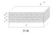
請參照第1圖至第10圖,第1圖至第10圖為本發明較佳實施例製作一奈米線電晶體之方法示意圖。如第1圖所示,首先提供一基底12,例如一矽基底,然後形成一堆疊結構14於基底12上。在本實施例中,堆疊結構14較佳由複數個第一半導體層16、18、20與第二半導體層22、24、26交錯堆疊而成。其中第一半導體層16、18、20與第二半導體層22、24、26較佳包含不同材料或不同晶格常數,且第一半導體層16、18、20與第二半導體層22、24、26均可選自由矽、鍺、摻雜矽、摻雜鍺以及鍺化矽所構成的群組。需注意的是,本實施例所揭露之堆疊結構雖以三層第一半導體層16、18、20交錯三層第二半導體層22、24、26為例,但第一半導體層16、18、20與第二半導體層22、24、26的數量並不侷限於此,而可視製程或產品需求任意調整。Please refer to FIGS. 1 to 10, FIGS. 1 to 10 are schematic diagrams of a method for manufacturing a nanowire transistor according to a preferred embodiment of the present invention. As shown in FIG. 1, a
如第2圖所示,接著進行一微影暨蝕刻製程,例如利用一圖案化光阻(圖未示)為遮罩去除部分堆疊結構14與部分的基底12,以於基底12上形成凹槽28。然後於部分基底12上的凹槽28中形成一介電層30用來電性隔絕被圖案化的堆疊結構14,並使介電層30上表面切齊最下層的第一半導體層16下表面。在本實施例中,介電層30可由氧化矽所構成,但不侷限於此。As shown in FIG. 2, a photolithography and etching process is then performed, for example, a patterned photoresist (not shown) is used as a mask to remove part of the
隨後如第3圖所示,形成一硬遮罩32或犧牲閘極結構橫跨堆疊結構14,並接著形成一側壁子34於硬遮罩32側壁。在本實施例中,硬遮罩32可由多晶矽所構成,側壁子34可選自由二氧化矽、氮化矽、氮氧化矽以及氮碳化矽所構成的群組,但不侷限於此。另外需注意的是,本實施例之側壁子34雖為一單層側壁子,但又可視製程需求為複合式側壁子。舉例來說,側壁子34又可細部包含一個或一個以上的側壁子,且複合式的側壁子之間可選擇為相同或不同材料。依據本發明之一實施例,複合式側壁子可包含例如一由二氧化矽與氮化矽一同構成的雙層複合式側壁子,或是由氧化矽-氮化矽-氧化矽所構成的三層複合式側壁子,這些均屬本發明所涵蓋的範圍。Then, as shown in FIG. 3, a
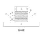
請接著參照第4圖及第5圖,其中第5圖為接續第4圖沿著切線AA'之剖面示意圖。如第4圖及第5圖所示,進行一微影暨蝕刻製程或直接以硬遮罩32為遮罩去除側壁子34兩側的部分堆疊結構14以形成凹槽36。Please refer to FIG. 4 and FIG. 5, wherein FIG. 5 is a schematic cross-sectional view along the tangent line AA′ following FIG. 4. As shown in FIG. 4 and FIG. 5, a lithography and etching process is performed or the
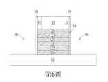
然後如第6圖所示,先覆蓋一材料層(圖未示)於基底12表面、堆疊結構14側壁以及硬遮罩32上,並以回蝕刻去除部分材料層以形成另一側壁子38於側壁子34與堆疊結構14旁,其中側壁子38與側壁子34較佳為不同材料,例如本實施例的側壁子38較佳由一金屬氧化物介電材料或高介電常數介電材料所構成,但不侷限於此。Then, as shown in FIG. 6, a material layer (not shown) is first covered on the surface of the
在本實施例中,用來構成側壁子38的金屬氧化物介電材料或高介電常數介電層包含介電常數大於4的介電材料,例如係選自氧化鉿(hafnium oxide,HfO2)、矽酸鉿氧化合物(hafnium silicon oxide,HfSiO4)、矽酸鉿氮氧化合物(hafnium silicon oxynitride,HfSiON)、氧化鋁(aluminum oxide,Al2O3)、氧化鑭(lanthanum oxide,La2O3)、氧化鉭(tantalum oxide,Ta2O5)、氧化釔(yttrium oxide,Y2O3)、氧化鋯(zirconium oxide,ZrO2)、鈦酸鍶(strontium titanate oxide,SrTiO3)、矽酸鋯氧化合物(zirconium silicon oxide,ZrSiO4)、鋯酸鉿(hafnium zirconium oxide,HfZrO4)、鍶鉍鉭氧化物(strontium bismuth tantalate,SrBi2Ta2O9,SBT)、鋯鈦酸鉛(lead zirconate titanate,PbZrxTi1-xO3,PZT)、鈦酸鋇鍶(barium strontium titanate,BaxSr1-xTiO3,BST)、或其組合所組成之群組。In this embodiment, the metal oxide dielectric material or high dielectric constant dielectric layer used to form the
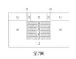
如第7圖所示,接著形成一源極/汲極結構40於側壁子38兩側的基底12上,其中源極/汲極結構40可由半導體材料或金屬材料所構成。在本實施例中,若源極/汲極結構40由半導體材料所構成,其可選自由鍺、摻雜矽、摻雜鍺以及鍺化矽所構成的群組。若源極/汲極結構40由金屬所構成,其可選自由鎢、鈦、氮化鈦、鉭、氮化鉭以及鋁所構成的群組。As shown in FIG. 7, a source/
隨後形成一層間介電層42於源極/汲極結構40上並環繞側壁子38,然後進行一平坦化製程,例如利用CMP去除部分層間介電層42,使剩餘的層間介電層42上表面切齊硬遮罩32上表面。在本實施例中,層間介電層42可由任何包含氧化物之絕緣材料所構成,例如一由四乙氧基矽烷(Tetraethyl orthosilicate,TEOS)所構成的氧化層,但不侷限於此。Then, an
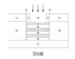
如第8圖所示,接著先進行一蝕刻製程去除硬遮罩32以形成開口44,然後再進行另一選擇性蝕刻製程去除第一半導體層16、18、20以形成複數個開口46。由於第一半導體層16、18、20與第二半導體層22、24、26由不同材料所構成且兩者之間具有一預定的蝕刻選擇比,本實施例較佳以蝕刻去除第一半導體層16、18、20時不損害任何第二半導體層22、24、26。As shown in FIG. 8, an etching process is first performed to remove the
依據本發明之一實施例,第一半導體層16、18、20與硬遮罩32又可由相同材料所構成,例如均包含多晶矽而第二半導體層22、24、26則可選自由單晶矽、鍺、摻雜矽、摻雜鍺以及鍺化矽所構成的群組,如此便可利用一道蝕刻製程同時去除硬遮罩32與第一半導體層16、18、20,此實施例也屬本發明所涵蓋的範圍。另外以蝕刻製程去除第一半導體層16、18、20之後,可再選擇性利用氧化或另一道蝕刻去除部分第二半導體層22、24、26,將原本約略四方體的第二半導體層22、24、26蝕刻成約略圓弧狀而構成奈米通道層,此實施例也屬本發明所涵蓋的範圍。According to an embodiment of the present invention, the first semiconductor layers 16, 18, 20 and the
隨後如第9圖所示,依序形成一高介電常數介電層48、一功函數金屬層50以及一低阻抗金屬層52於開口44及開口46內,再平坦化以形成一閘極結構54。在本實施例中,閘極結構54較佳包含兩部分,其中第一部分56設於第二半導體層22、24、26正上方而第二部分58則與第二半導體層22、24、26交錯設置。從另一角度來看,高介電常數介電層48與功函數金屬層50包覆第二半導體層22、24、26,而低阻抗金屬層52填滿於開口44及開口46內。Then, as shown in FIG. 9, a high dielectric
在本實施例中,高介電常數介電層48包含介電常數大於4的介電材料,例如係選自氧化鉿(hafnium oxide,HfO2)、矽酸鉿氧化合物(hafnium silicon oxide,HfSiO4)、矽酸鉿氮氧化合物(hafnium silicon oxynitride,HfSiON)、氧化鋁(aluminum oxide,Al2O3)、氧化鑭(lanthanum oxide,La2O3)、氧化鉭(tantalum oxide,Ta2O5)、氧化釔(yttrium oxide,Y2O3)、氧化鋯(zirconium oxide,ZrO2)、鈦酸鍶(strontium titanate oxide,SrTiO3)、矽酸鋯氧化合物(zirconium silicon oxide,ZrSiO4)、鋯酸鉿(hafnium zirconium oxide,HfZrO4)、鍶鉍鉭氧化物(strontium bismuth tantalate,SrBi2Ta2O9,SBT)、鋯鈦酸鉛(lead zirconate titanate,PbZrxTi1-xO3,PZT)、鈦酸鋇鍶(barium strontium titanate,BaxSr1-xTiO3,BST)、或其組合所組成之群組。In this embodiment, the high dielectric
功函數金屬層50較佳用以調整形成金屬閘極之功函數,使其適用於N型電晶體(NMOS)或P型電晶體(PMOS)。若電晶體為N型電晶體,功函數金屬層50可選用功函數為3.9電子伏特(eV)~4.3eV的金屬材料,如鋁化鈦(TiAl)、鋁化鋯(ZrAl)、鋁化鎢(WAl)、鋁化鉭(TaAl)、鋁化鉿(HfAl)或TiAlC(碳化鈦鋁)等,但不以此為限;若電晶體為P型電晶體,功函數金屬層50可選用功函數為4.8eV~5.2eV的金屬材料,如氮化鈦(TiN)、氮化鉭(TaN)或碳化鉭(TaC)等,但不以此為限。功函數金屬層50與低阻抗金屬層52之間可包含另一阻障層(圖未示),其中阻障層的材料可包含鈦(Ti)、氮化鈦(TiN)、鉭(Ta)、氮化鉭(TaN)等材料。低阻抗金屬層52則可選自銅(Cu)、鋁(Al)、鎢(W)、鈦鋁合金(TiAl)、鈷鎢磷化物(cobalt tungsten phosphide,CoWP)等低電阻材料或其組合。由於依據金屬閘極置換製程將虛置閘極轉換為金屬閘極乃此領域者所熟知技藝,在此不另加贅述。The work
之後可去除部分高介電常數介電層48、部分功函數金屬層50與部分低阻抗金屬層52形成凹槽(圖未示),然後再填入一硬遮罩60於凹槽內並使硬遮罩60與層間介電層42表面齊平,其中硬遮罩60可選自由氧化矽、氮化矽、氮氧化矽以及氮碳化矽所構成的群組。After that, part of the high dielectric
如第10圖所示,然後進行一自行對準接觸插塞製程形成接觸插塞62電連接源極/汲極結構40。在本實施例中,形成接觸插塞62的方式可先利用一蝕刻製程完全去除層間介電層42形成開口(圖未示)並暴露出源極/汲極結構40表面,然後依序沉積一阻障層64與一金屬層66於開口內並填滿開口,然後利用一平坦化製程,例如以CMP製程去除部分金屬層66與部分阻障層64,以於開口中形成接觸插塞62,其中接觸插塞62上表面較佳與閘極結構54上表面切齊。在本實施例中,阻障層64較佳選自由鈦、鉭、氮化鈦、氮化鉭以及氮化鎢所構成的群組,金屬層66較佳選自由鋁、鈦、鉭、鎢、鈮、鉬以及銅所構成的群組,但不侷限於此。至此即完成本發明較佳實施例之一半導體元件的製作。As shown in FIG. 10, a self-aligned contact plug process is then formed to form the
另外在本實施例中,第二半導體層22、24、26較佳作為奈米通道層,且若源極/汲極結構40由金屬所構成,源極/汲極結構40較佳與側壁子38以及第二半導體層22、24、26構成一金屬絕緣體半導體(metal-insulator-semiconductor,MIS)。若源極/汲極結構40由半導體材料所構成,則接觸插塞62中可另形成一絕緣層使源極/汲極結構40、接觸插塞62中的絕緣層以及接觸插塞62中的金屬材料構成另一組金屬絕緣體半導體。In addition, in this embodiment, the second semiconductor layers 22, 24, and 26 are preferably used as nano-channel layers, and if the source/
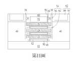
請繼續參照第11圖,第11圖為本發明另一實施例之一奈米線電晶體之結構示意圖。如第11圖所示,相較於第5圖至第6圖去除部分堆疊結構14形成凹槽36後便直接形成側壁子38,本實施例可選擇在形成側壁子38之前額外進行一道蝕刻製程去除部分第一半導體層16、18、20,使各第一半導體層16、18、20的寬度小於各第二半導體層22、24、26的寬度而構成一階梯狀的邊緣或側壁。由於第一半導體層16、18、20與第二半導體層22、24、26的側壁在蝕刻後已不切齊,後續所形成的側壁子38也會順勢沿著第一半導體層16、18、20與第二半導體層22、24、26的邊緣而形成凹凸的輪廓。之後可比照第6圖至第9圖的製程形成源極/汲極結構40與層間介電層42,掏空硬遮罩32與第一半導體層16、18、20形成開口,填入高介電常數介電層48、功函數金屬層50以及低阻抗金屬層52形成閘極結構54,以及形成電連接源極/汲極結構40的接觸插塞62。Please continue to refer to FIG. 11, which is a schematic structural view of a nanowire transistor according to another embodiment of the present invention. As shown in FIG. 11, compared with FIGS. 5 to 6, after removing a part of the stacked
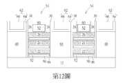
請繼續參照第12圖,第12圖為本發明另一實施例之一奈米線電晶體之結構示意圖。如第12圖所示,相較於第10圖之單閘極奈米線電晶體結構,本實施例揭露一種雙閘極奈米線電晶體結構,其主要包含兩組閘極結構54設於基底12上,其中各閘極結構54與前述實施例中的閘極結構54具有相同組成,例如各包含高介電常數介電層48、功函數金屬層50以及低阻抗金屬層52。在本實施例中,兩組閘極結構54之間設有一共用之源極/汲極結構68,且原本設於閘極結構54兩側之源極/汲極結構40與源極/汲極結構68均各自電連接至一接觸插塞62。Please continue to refer to FIG. 12, which is a schematic structural view of a nanowire transistor according to another embodiment of the present invention. As shown in Figure 12, compared to the single gate nanowire in Figure 10Transistor structure, this embodiment discloses a double gate nanowire transistor structure, which mainly includes two groups of
請繼續參照第13圖,第13圖為本發明另一實施例之一奈米線電晶體之結構示意圖。如第13圖所示,相較於第10圖之單閘極奈米線電晶體結構,本實施例揭露一種雙閘極奈米線電晶體結構,其主要包含兩組閘極結構54分別設於基底12上的NMOS區域72及PMOS區域74,其中各閘極結構54與前述實施例中的閘極結構54具有相同組成,例如各包含高介電常數介電層48、功函數金屬層50以及低阻抗金屬層52。在本實施例中,NMOS區域72的源極/汲極結構76較佳由金屬所構成,且與NMOS區域72的側壁子80及第二半導體層22、24、26構成一金屬絕緣體半導體。其中NMOS區域72的側壁子80較佳與PMOS區域74的側壁子38為不同材料,但兩者均可包含金屬氧化物介電材料以及/或高介電常數介電材料。Please continue to refer to FIG. 13, which is a schematic structural view of a nanowire transistor according to another embodiment of the present invention. As shown in FIG. 13, compared with the single gate nanowire transistor structure of FIG. 10, this embodiment discloses a double gate nanowire transistor structure, which mainly includes two sets of
PMOS區域74的源極/汲極結構78則較佳由半導體材料所構成,例如鍺化矽所構成,且PMOS區域74的接觸插塞62中可另形成一絕緣層使源極/汲極結構78、接觸插塞62中的絕緣層以及接觸插塞62中的金屬材料構成一組金屬絕緣體半導體。另外在本實施例中,NMOS區域72的接觸插塞62與源極/汲極結構76之間較佳無金屬矽化物,但PMOS區域74可包含一金屬矽化物82設於接觸插塞62與源極/汲極結構78之間,其中本實施例的金屬矽化物82底部雖低於第二半導體層26上表面,但不侷限於此,金屬矽化物82的底部又可依據製程需求高於第二半導體層26上表面,此實施例也屬本發明所涵蓋的範圍。以上所述僅為本發明之較佳實施例,凡依本發明申請專利範圍所做之均等變化與修飾,皆應屬本發明之涵蓋範圍。The source/
12:基底12: base
22:第二半導體層22: Second semiconductor layer
24:第二半導體層24: Second semiconductor layer
26:第二半導體層26: Second semiconductor layer
34:側壁子34: Side wall
38:側壁子38: Side wall
40:源極/汲極結構40: source/drain structure
48:高介電常數介電層48: High dielectric constant dielectric layer
50:功函數金屬層50: work function metal layer
52:低阻抗金屬層52: Low impedance metal layer
54:閘極結構54: Gate structure
56:第一部分56: Part One
58:第二部分58: Part Two
60:硬遮罩60: hard mask
62:接觸插塞62: contact plug
64:阻障層64: barrier layer
66:金屬層66: metal layer
Claims (19)
Translated fromChinesePriority Applications (3)
| Application Number | Priority Date | Filing Date | Title |
|---|---|---|---|
| TW105110463ATWI686351B (en) | 2016-04-01 | 2016-04-01 | Nanowire transistor and method for fabricating the same |
| US15/146,898US10068969B2 (en) | 2016-04-01 | 2016-05-05 | Nanowire transistor and method for fabricating the same |
| US16/053,794US10381439B2 (en) | 2016-04-01 | 2018-08-02 | Nanowire transistor having two spacers between gate structure and source/drain structure |
Applications Claiming Priority (1)
| Application Number | Priority Date | Filing Date | Title |
|---|---|---|---|
| TW105110463ATWI686351B (en) | 2016-04-01 | 2016-04-01 | Nanowire transistor and method for fabricating the same |
Publications (2)
| Publication Number | Publication Date |
|---|---|
| TW201736249A TW201736249A (en) | 2017-10-16 |
| TWI686351Btrue TWI686351B (en) | 2020-03-01 |
Family
ID=59961228
Family Applications (1)
| Application Number | Title | Priority Date | Filing Date |
|---|---|---|---|
| TW105110463ATWI686351B (en) | 2016-04-01 | 2016-04-01 | Nanowire transistor and method for fabricating the same |
Country Status (2)
| Country | Link |
|---|---|
| US (2) | US10068969B2 (en) |
| TW (1) | TWI686351B (en) |
Families Citing this family (24)
| Publication number | Priority date | Publication date | Assignee | Title |
|---|---|---|---|---|
| US11004985B2 (en)* | 2016-05-30 | 2021-05-11 | Samsung Electronics Co., Ltd. | Semiconductor device having multi-thickness nanowire |
| US10236362B2 (en)* | 2016-06-30 | 2019-03-19 | International Business Machines Corporation | Nanowire FET including nanowire channel spacers |
| KR102574454B1 (en) | 2016-12-16 | 2023-09-04 | 삼성전자 주식회사 | Semiconductor devices and method of manufacturing the same |
| US10128347B2 (en)* | 2017-01-04 | 2018-11-13 | International Business Machines Corporation | Gate-all-around field effect transistor having multiple threshold voltages |
| US11245020B2 (en) | 2017-01-04 | 2022-02-08 | International Business Machines Corporation | Gate-all-around field effect transistor having multiple threshold voltages |
| US10297663B2 (en)* | 2017-04-19 | 2019-05-21 | International Business Machines Corporation | Gate fill utilizing replacement spacer |
| KR20230006054A (en)* | 2017-11-30 | 2023-01-10 | 인텔 코포레이션 | Fin patterning for advanced integrated circuit structure fabrication |
| US10340341B1 (en)* | 2017-12-20 | 2019-07-02 | International Business Machines Corporation | Self-limiting and confining epitaxial nucleation |
| US10896956B2 (en)* | 2017-12-22 | 2021-01-19 | Commissariat A L'energie Atomique Et Aux Energies Alternatives | Field effect transistor with reduced contact resistance |
| US11245005B2 (en) | 2018-05-14 | 2022-02-08 | Taiwan Semiconductor Manufacturing Co., Ltd. | Method for manufacturing semiconductor structure with extended contact structure |
| US10522622B2 (en) | 2018-05-14 | 2019-12-31 | Taiwan Semiconductor Manufacturing Co., Ltd. | Multi-gate semiconductor device and method for forming the same |
| CN112437978A (en)* | 2018-07-26 | 2021-03-02 | 索尼半导体解决方案公司 | Semiconductor device with a plurality of semiconductor chips |
| KR102571567B1 (en) | 2018-11-02 | 2023-08-29 | 삼성전자주식회사 | Semiconductor device |
| US10930755B2 (en) | 2018-11-26 | 2021-02-23 | Taiwan Semiconductor Manufacturing Co., Ltd. | Self-aligned inner spacer on gate-all-around structure and methods of forming the same |
| US11183574B2 (en) | 2019-05-24 | 2021-11-23 | Taiwan Semiconductor Manufacturing Co., Ltd. | Work function layers for transistor gate electrodes |
| US11165032B2 (en)* | 2019-09-05 | 2021-11-02 | Taiwan Semiconductor Manufacturing Co., Ltd. | Field effect transistor using carbon nanotubes |
| KR102857206B1 (en) | 2019-10-02 | 2025-09-11 | 삼성전자주식회사 | Semiconductor device |
| US11495661B2 (en) | 2020-04-07 | 2022-11-08 | Taiwan Semiconductor Manufacturing Company, Ltd. | Semiconductor device including gate barrier layer |
| KR20210124731A (en)* | 2020-04-07 | 2021-10-15 | 삼성전자주식회사 | Semiconductor devices including gate spacer |
| US11538809B2 (en)* | 2020-08-31 | 2022-12-27 | Micron Technology, Inc. | Metal insulator semiconductor (MIS) contact in three dimensional (3D) vertical memory |
| CN114792682A (en)* | 2021-01-26 | 2022-07-26 | 联华电子股份有限公司 | Nanowire transistor and method of making the same |
| US11715762B2 (en) | 2021-01-28 | 2023-08-01 | Taiwan Semiconductor Manufacturing Co., Ltd. | Transistor gate structures and methods of forming the same |
| CN113178488B (en)* | 2021-03-03 | 2023-09-19 | 中国科学院微电子研究所 | Preparation method of semiconductor device and semiconductor device |
| KR20230037989A (en)* | 2021-09-10 | 2023-03-17 | 삼성전자주식회사 | Multi bridge channel field effect transistor and method of fabricating the same |
Citations (2)
| Publication number | Priority date | Publication date | Assignee | Title |
|---|---|---|---|---|
| US9252252B2 (en)* | 2012-05-23 | 2016-02-02 | Ecole polytechnique fédérale de Lausanne (EPFL) | Ambipolar silicon nanowire field effect transistor |
| US20160043085A1 (en)* | 2013-08-01 | 2016-02-11 | Taiwan Semiconductor Manufacturing Company, Ltd. | Semiconductor Device And Fabricating The Same |
Family Cites Families (17)
| Publication number | Priority date | Publication date | Assignee | Title |
|---|---|---|---|---|
| US8497528B2 (en) | 2010-05-06 | 2013-07-30 | Taiwan Semiconductor Manufacturing Company, Ltd. | Method for fabricating a strained structure |
| US8173993B2 (en) | 2009-12-04 | 2012-05-08 | International Business Machines Corporation | Gate-all-around nanowire tunnel field effect transistors |
| US8853709B2 (en) | 2011-07-29 | 2014-10-07 | Hrl Laboratories, Llc | III-nitride metal insulator semiconductor field effect transistor |
| US8901659B2 (en)* | 2012-02-09 | 2014-12-02 | International Business Machines Corporation | Tapered nanowire structure with reduced off current |
| US9006829B2 (en) | 2012-08-24 | 2015-04-14 | Taiwan Semiconductor Manufacturing Company, Ltd. | Aligned gate-all-around structure |
| US8802512B2 (en)* | 2013-01-11 | 2014-08-12 | International Business Machines Corporation | Overlap capacitance nanowire |
| KR102037304B1 (en)* | 2013-03-15 | 2019-10-29 | 인텔 코포레이션 | Nanowire transistor with underlayer etch stops |
| US9035277B2 (en)* | 2013-08-01 | 2015-05-19 | Taiwan Semiconductor Manufacturing Company, Ltd. | Semiconductor device and fabricating the same |
| US20150270134A1 (en) | 2014-03-19 | 2015-09-24 | Qualcomm Incorporated | Methods of forming a metal-insulator-semiconductor (mis) structure and a dual contact device |
| US9263580B2 (en) | 2014-03-24 | 2016-02-16 | Globalfoundries Inc. | Methods of forming isolated channel regions for a FinFET semiconductor device and the resulting device |
| US20150333162A1 (en)* | 2014-05-16 | 2015-11-19 | Globalfoundries Inc. | Methods of forming nanowire devices with metal-insulator-semiconductor source/drain contacts and the resulting devices |
| US9548358B2 (en)* | 2014-05-19 | 2017-01-17 | International Business Machines Corporation | Dual fill silicon-on-nothing field effect transistor |
| KR102158963B1 (en) | 2014-05-23 | 2020-09-24 | 삼성전자 주식회사 | Semiconductor device and fabricated method thereof |
| US9490340B2 (en) | 2014-06-18 | 2016-11-08 | Globalfoundries Inc. | Methods of forming nanowire devices with doped extension regions and the resulting devices |
| US9502518B2 (en) | 2014-06-23 | 2016-11-22 | Stmicroelectronics, Inc. | Multi-channel gate-all-around FET |
| US9620601B2 (en) | 2014-07-01 | 2017-04-11 | Taiwan Semiconductor Manufacturing Company, Ltd. | Contact structures and methods of forming the same |
| US9647098B2 (en) | 2014-07-21 | 2017-05-09 | Samsung Electronics Co., Ltd. | Thermionically-overdriven tunnel FETs and methods of fabricating the same |
- 2016
- 2016-04-01TWTW105110463Apatent/TWI686351B/enactive
- 2016-05-05USUS15/146,898patent/US10068969B2/enactiveActive
- 2018
- 2018-08-02USUS16/053,794patent/US10381439B2/enactiveActive
Patent Citations (2)
| Publication number | Priority date | Publication date | Assignee | Title |
|---|---|---|---|---|
| US9252252B2 (en)* | 2012-05-23 | 2016-02-02 | Ecole polytechnique fédérale de Lausanne (EPFL) | Ambipolar silicon nanowire field effect transistor |
| US20160043085A1 (en)* | 2013-08-01 | 2016-02-11 | Taiwan Semiconductor Manufacturing Company, Ltd. | Semiconductor Device And Fabricating The Same |
Also Published As
| Publication number | Publication date |
|---|---|
| TW201736249A (en) | 2017-10-16 |
| US20180342581A1 (en) | 2018-11-29 |
| US20170288018A1 (en) | 2017-10-05 |
| US10381439B2 (en) | 2019-08-13 |
| US10068969B2 (en) | 2018-09-04 |
Similar Documents
| Publication | Publication Date | Title |
|---|---|---|
| TWI686351B (en) | Nanowire transistor and method for fabricating the same | |
| CN106803484B (en) | Semiconductor element and manufacturing method thereof | |
| TWI675406B (en) | Semiconductor device and method for fabricating the same | |
| TWI716601B (en) | Semiconductor device and method for fabricating the same | |
| CN106684041B (en) | Semiconductor device and method of making the same | |
| CN107346739A (en) | Semiconductor element and manufacturing method thereof | |
| CN109216191B (en) | Semiconductor element and manufacturing method thereof | |
| CN107808849B (en) | Semiconductor device and method of making the same | |
| TWI632617B (en) | Semiconductor component and manufacturing method thereof | |
| TWI776911B (en) | Semiconductor device and method for fabricating the same | |
| CN111769045B (en) | Semiconductor element and manufacturing method thereof | |
| TWI729181B (en) | Semiconductor device and method for fabricating the same | |
| TWI728162B (en) | Semiconductor device and method for fabricating the same | |
| US12027600B2 (en) | Nanowire transistor and method for fabricating the same | |
| CN107305866A (en) | Semiconductor element and manufacturing method thereof | |
| CN106683990A (en) | Semiconductor element and manufacturing method thereof | |
| TW202347452A (en) | Semiconductor device and method for fabricating the same | |
| CN112736079A (en) | Semiconductor device having contact plug connected to gate structure of PMOS region | |
| CN109728080B (en) | Tunnel field effect transistor and manufacturing method thereof | |
| CN115206802A (en) | Laterally diffused metal oxide semiconductor device and method of making the same | |
| CN106340540B (en) | Semiconductor element and method for filling pattern | |
| CN114597129A (en) | Semiconductor element and manufacturing method thereof | |
| TW202015112A (en) | Semiconductor element and its manufacturing method | |
| CN115910786A (en) | Semiconductor element and manufacturing method thereof | |
| TWI887076B (en) | Semiconductor device and method for fabricating the same |