TWI683407B - Substrate structure and method for fabricating the same - Google Patents
Substrate structure and method for fabricating the sameDownload PDFInfo
- Publication number
- TWI683407B TWI683407BTW106117021ATW106117021ATWI683407BTW I683407 BTWI683407 BTW I683407BTW 106117021 ATW106117021 ATW 106117021ATW 106117021 ATW106117021 ATW 106117021ATW I683407 BTWI683407 BTW I683407B
- Authority
- TW
- Taiwan
- Prior art keywords
- substrate structure
- layer
- item
- patent application
- rough surface
- Prior art date
Links
- 239000000758substrateSubstances0.000titleclaimsabstractdescription74
- 238000000034methodMethods0.000titleclaimsabstractdescription27
- 238000004519manufacturing processMethods0.000claimsabstractdescription28
- 239000010410layerSubstances0.000claimsdescription131
- 229910052751metalInorganic materials0.000claimsdescription19
- 239000002184metalSubstances0.000claimsdescription19
- 238000000708deep reactive-ion etchingMethods0.000claimsdescription14
- 239000011241protective layerSubstances0.000claimsdescription13
- 238000007788rougheningMethods0.000claimsdescription5
- 229920002120photoresistant polymerPolymers0.000claimsdescription4
- 230000015572biosynthetic processEffects0.000claims1
- 239000000126substanceSubstances0.000claims1
- 239000000463materialSubstances0.000abstractdescription9
- 230000032798delaminationEffects0.000abstractdescription5
- 239000008393encapsulating agentSubstances0.000abstract1
- 230000002708enhancing effectEffects0.000abstract1
- 235000019592roughnessNutrition0.000description21
- 229910052710siliconInorganic materials0.000description20
- 239000010703siliconSubstances0.000description20
- XUIMIQQOPSSXEZ-UHFFFAOYSA-NSiliconChemical compound[Si]XUIMIQQOPSSXEZ-UHFFFAOYSA-N0.000description18
- 239000004065semiconductorSubstances0.000description14
- 230000008569processEffects0.000description10
- 229910000679solderInorganic materials0.000description8
- 238000004806packaging method and processMethods0.000description5
- 239000000853adhesiveSubstances0.000description4
- 230000001070adhesive effectEffects0.000description4
- 239000013078crystalSubstances0.000description4
- 238000005516engineering processMethods0.000description4
- 238000009413insulationMethods0.000description4
- RYGMFSIKBFXOCR-UHFFFAOYSA-NCopperChemical compound[Cu]RYGMFSIKBFXOCR-UHFFFAOYSA-N0.000description3
- 230000008859changeEffects0.000description3
- 230000000052comparative effectEffects0.000description3
- 229910052802copperInorganic materials0.000description3
- 239000010949copperSubstances0.000description3
- 238000012858packaging processMethods0.000description3
- 239000000047productSubstances0.000description3
- 239000007787solidSubstances0.000description3
- 238000012546transferMethods0.000description3
- PXHVJJICTQNCMI-UHFFFAOYSA-NNickelChemical compound[Ni]PXHVJJICTQNCMI-UHFFFAOYSA-N0.000description2
- 239000004642PolyimideSubstances0.000description2
- RTAQQCXQSZGOHL-UHFFFAOYSA-NTitaniumChemical compound[Ti]RTAQQCXQSZGOHL-UHFFFAOYSA-N0.000description2
- 238000005336crackingMethods0.000description2
- 230000000694effectsEffects0.000description2
- 239000011521glassSubstances0.000description2
- 229920001721polyimidePolymers0.000description2
- 239000010936titaniumSubstances0.000description2
- 229910052719titaniumInorganic materials0.000description2
- 230000007704transitionEffects0.000description2
- 229910052581Si3N4Inorganic materials0.000description1
- 229910004298SiO 2Inorganic materials0.000description1
- VYPSYNLAJGMNEJ-UHFFFAOYSA-NSilicium dioxideChemical compoundO=[Si]=OVYPSYNLAJGMNEJ-UHFFFAOYSA-N0.000description1
- UMIVXZPTRXBADB-UHFFFAOYSA-NbenzocyclobuteneChemical compoundC1=CC=C2CCC2=C1UMIVXZPTRXBADB-UHFFFAOYSA-N0.000description1
- 239000007795chemical reaction productSubstances0.000description1
- 230000007547defectEffects0.000description1
- 238000011161developmentMethods0.000description1
- 238000010586diagramMethods0.000description1
- 239000003989dielectric materialSubstances0.000description1
- 239000003292glueSubstances0.000description1
- 230000004048modificationEffects0.000description1
- 238000012986modificationMethods0.000description1
- 229910052759nickelInorganic materials0.000description1
- HBVFXTAPOLSOPB-UHFFFAOYSA-Nnickel vanadiumChemical compound[V].[Ni]HBVFXTAPOLSOPB-UHFFFAOYSA-N0.000description1
- 150000004767nitridesChemical class0.000description1
- 238000000059patterningMethods0.000description1
- 238000007747platingMethods0.000description1
- 229920002577polybenzoxazolePolymers0.000description1
- 230000035945sensitivityEffects0.000description1
- HQVNEWCFYHHQES-UHFFFAOYSA-Nsilicon nitrideChemical compoundN12[Si]34N5[Si]62N3[Si]51N64HQVNEWCFYHHQES-UHFFFAOYSA-N0.000description1
- 229910052814silicon oxideInorganic materials0.000description1
- 239000002210silicon-based materialSubstances0.000description1
- 238000004544sputter depositionMethods0.000description1
- 230000003746surface roughnessEffects0.000description1
- 238000012360testing methodMethods0.000description1
Images


Classifications
- H—ELECTRICITY
- H01—ELECTRIC ELEMENTS
- H01L—SEMICONDUCTOR DEVICES NOT COVERED BY CLASS H10
- H01L23/00—Details of semiconductor or other solid state devices
- H01L23/48—Arrangements for conducting electric current to or from the solid state body in operation, e.g. leads, terminal arrangements ; Selection of materials therefor
- H01L23/488—Arrangements for conducting electric current to or from the solid state body in operation, e.g. leads, terminal arrangements ; Selection of materials therefor consisting of soldered or bonded constructions
- H01L23/498—Leads, i.e. metallisations or lead-frames on insulating substrates, e.g. chip carriers
- H01L23/49838—Geometry or layout
- H—ELECTRICITY
- H01—ELECTRIC ELEMENTS
- H01L—SEMICONDUCTOR DEVICES NOT COVERED BY CLASS H10
- H01L21/00—Processes or apparatus adapted for the manufacture or treatment of semiconductor or solid state devices or of parts thereof
- H01L21/02—Manufacture or treatment of semiconductor devices or of parts thereof
- H01L21/04—Manufacture or treatment of semiconductor devices or of parts thereof the devices having potential barriers, e.g. a PN junction, depletion layer or carrier concentration layer
- H01L21/48—Manufacture or treatment of parts, e.g. containers, prior to assembly of the devices, using processes not provided for in a single one of the groups H01L21/18 - H01L21/326 or H10D48/04 - H10D48/07
- H01L21/4814—Conductive parts
- H01L21/4846—Leads on or in insulating or insulated substrates, e.g. metallisation
- H—ELECTRICITY
- H01—ELECTRIC ELEMENTS
- H01L—SEMICONDUCTOR DEVICES NOT COVERED BY CLASS H10
- H01L2224/00—Indexing scheme for arrangements for connecting or disconnecting semiconductor or solid-state bodies and methods related thereto as covered by H01L24/00
- H01L2224/01—Means for bonding being attached to, or being formed on, the surface to be connected, e.g. chip-to-package, die-attach, "first-level" interconnects; Manufacturing methods related thereto
- H01L2224/10—Bump connectors; Manufacturing methods related thereto
- H01L2224/15—Structure, shape, material or disposition of the bump connectors after the connecting process
- H01L2224/16—Structure, shape, material or disposition of the bump connectors after the connecting process of an individual bump connector
- H01L2224/161—Disposition
- H01L2224/16151—Disposition the bump connector connecting between a semiconductor or solid-state body and an item not being a semiconductor or solid-state body, e.g. chip-to-substrate, chip-to-passive
- H01L2224/16221—Disposition the bump connector connecting between a semiconductor or solid-state body and an item not being a semiconductor or solid-state body, e.g. chip-to-substrate, chip-to-passive the body and the item being stacked
- H01L2224/16225—Disposition the bump connector connecting between a semiconductor or solid-state body and an item not being a semiconductor or solid-state body, e.g. chip-to-substrate, chip-to-passive the body and the item being stacked the item being non-metallic, e.g. insulating substrate with or without metallisation
- H—ELECTRICITY
- H01—ELECTRIC ELEMENTS
- H01L—SEMICONDUCTOR DEVICES NOT COVERED BY CLASS H10
- H01L2224/00—Indexing scheme for arrangements for connecting or disconnecting semiconductor or solid-state bodies and methods related thereto as covered by H01L24/00
- H01L2224/01—Means for bonding being attached to, or being formed on, the surface to be connected, e.g. chip-to-package, die-attach, "first-level" interconnects; Manufacturing methods related thereto
- H01L2224/26—Layer connectors, e.g. plate connectors, solder or adhesive layers; Manufacturing methods related thereto
- H01L2224/31—Structure, shape, material or disposition of the layer connectors after the connecting process
- H01L2224/32—Structure, shape, material or disposition of the layer connectors after the connecting process of an individual layer connector
- H01L2224/321—Disposition
- H01L2224/32151—Disposition the layer connector connecting between a semiconductor or solid-state body and an item not being a semiconductor or solid-state body, e.g. chip-to-substrate, chip-to-passive
- H01L2224/32221—Disposition the layer connector connecting between a semiconductor or solid-state body and an item not being a semiconductor or solid-state body, e.g. chip-to-substrate, chip-to-passive the body and the item being stacked
- H01L2224/32225—Disposition the layer connector connecting between a semiconductor or solid-state body and an item not being a semiconductor or solid-state body, e.g. chip-to-substrate, chip-to-passive the body and the item being stacked the item being non-metallic, e.g. insulating substrate with or without metallisation
- H—ELECTRICITY
- H01—ELECTRIC ELEMENTS
- H01L—SEMICONDUCTOR DEVICES NOT COVERED BY CLASS H10
- H01L2224/00—Indexing scheme for arrangements for connecting or disconnecting semiconductor or solid-state bodies and methods related thereto as covered by H01L24/00
- H01L2224/73—Means for bonding being of different types provided for in two or more of groups H01L2224/10, H01L2224/18, H01L2224/26, H01L2224/34, H01L2224/42, H01L2224/50, H01L2224/63, H01L2224/71
- H01L2224/732—Location after the connecting process
- H01L2224/73201—Location after the connecting process on the same surface
- H01L2224/73203—Bump and layer connectors
- H01L2224/73204—Bump and layer connectors the bump connector being embedded into the layer connector
- H—ELECTRICITY
- H01—ELECTRIC ELEMENTS
- H01L—SEMICONDUCTOR DEVICES NOT COVERED BY CLASS H10
- H01L2924/00—Indexing scheme for arrangements or methods for connecting or disconnecting semiconductor or solid-state bodies as covered by H01L24/00
- H01L2924/15—Details of package parts other than the semiconductor or other solid state devices to be connected
- H01L2924/151—Die mounting substrate
- H01L2924/153—Connection portion
- H01L2924/1531—Connection portion the connection portion being formed only on the surface of the substrate opposite to the die mounting surface
- H01L2924/15311—Connection portion the connection portion being formed only on the surface of the substrate opposite to the die mounting surface being a ball array, e.g. BGA
Landscapes
- Engineering & Computer Science (AREA)
- Physics & Mathematics (AREA)
- Condensed Matter Physics & Semiconductors (AREA)
- General Physics & Mathematics (AREA)
- Computer Hardware Design (AREA)
- Microelectronics & Electronic Packaging (AREA)
- Power Engineering (AREA)
- Geometry (AREA)
- Ceramic Engineering (AREA)
- Manufacturing & Machinery (AREA)
- Internal Circuitry In Semiconductor Integrated Circuit Devices (AREA)
- Manufacturing Of Printed Wiring (AREA)
Abstract
Description
Translated fromChinese本發明係有關一種半導體封裝結構,尤指一種基板結構。The invention relates to a semiconductor packaging structure, especially a substrate structure.
目前應用於晶片封裝領域之技術繁多,例如晶片尺寸構裝(Chip Scale Package,簡稱CSP)、晶片直接貼附封裝(Direct Chip Attached,簡稱DCA)或多晶片模組封裝(Multi-Chip Module,簡稱MCM)等覆晶型態的封裝模組、或將晶片立體堆疊化整合為三維積體電路(3D IC)晶片堆疊技術等。There are many technologies currently used in the field of chip packaging, such as Chip Scale Package (CSP), Direct Chip Attached (DCA) or Multi-Chip Module (Multi-Chip Module, abbreviation) MCM) and other flip-chip packaging modules, or integrating the three-dimensional stacking of chips into a three-dimensional integrated circuit (3D IC) chip stacking technology.
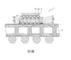
第1圖係為習知3D IC晶片堆疊之半導體封裝件1之剖面示意圖。如圖所示,該半導體封裝件1具有一矽中介板(Through Silicon interposer,簡稱TSI)10,該矽中介板10具有具有相對之置晶側10b與轉接側10a、及連通該置晶側10b與轉接側10a之複數導電矽穿孔(Through-silicon via,簡稱TSV)100,且該置晶側10b上具有一電性連接該些導電矽穿孔100之線路重佈結構(Redistribution layer,簡稱RDL)11,以供間距較小之半導體晶片5之電極墊50係藉由複數銲錫凸塊51電性結合至該線路重佈結構11上,且於各該導電矽穿孔100上藉由複數如銲料凸塊或銅柱之導電元件17電性結合間距較大之封裝基板7之銲墊70。FIG. 1 is a schematic cross-sectional view of a conventional semiconductor package 1 stacked on a 3D IC chip. As shown in the figure, the semiconductor package 1 has a through silicon interposer (TSI) 10, the
具體地,為了強固該半導體晶片5與該矽中介板10及該矽中介板10與該封裝基板7之間的接著強度,並保護該些銲錫凸塊51與該些導電元件17,故需於該半導體晶片5與該矽中介板10及該矽中介板10與該封裝基板7之間填充底膠(underfill)8,且該半導體晶片5與該矽中介板10之間的填充面積較小,故該半導體晶片5表面受到之應力較小,而該矽中介板10與該封裝基板7之間的填充面積較大,故該矽中介板10表面受到之應力較大。Specifically, in order to strengthen the bonding strength between the
惟,前述習知半導體封裝件1中,當應力變化時,如搬運、通過回銲爐、或經歷落摔等製程或測試時,該矽中介板10會形成較大的角落應力(Corner Stress),導致該矽中介板10之轉接側10a會沿角落處發生破裂(Crack)(如圖所示之破裂處k),故常於該矽中介板10之轉接側10a與該底膠8之間發生脫層(Delamination)問題,以致於產品可靠度不良。However, in the aforementioned conventional semiconductor package 1, when the stress changes, such as handling, passing through a reflow furnace, or undergoing a drop or other processes or tests, the
因此,如何克服上述習知技術的問題,實已成目前亟欲解決的問題。Therefore, how to overcome the above-mentioned problems of the conventional technology has become an urgent problem to be solved at present.
鑑於上述習知技術之種種缺失,本發明提供一種基板結構,係包括:基板本體;以及絕緣層,係形成於該基板本體上且具有一平坦面及一粗糙面,其中,該粗糙面之粗糙度係大於20埃米。In view of the above-mentioned defects of the prior art, the present invention provides a substrate structure including: a substrate body; and an insulating layer formed on the substrate body and having a flat surface and a rough surface, wherein the rough surface is thickThe roughness is greater than 20 Angstroms.
本發明復提供一種基板結構之製法,係包括:提供一表面形成有絕緣層之基板本體;形成圖案化阻層於該絕緣層上;以及移除該圖案化阻層,並令該圖案化阻層與該絕緣層之接觸面形成粗糙面,其中,該粗糙面之粗糙度係大於20埃米。The invention further provides a method for manufacturing a substrate structure, comprising: providing a substrate body with an insulating layer formed on its surface; forming a patterned resistive layer on the insulating layer; and removing the patterned resistive layer and making the patterned resistive The contact surface of the layer and the insulating layer forms a rough surface, wherein the roughness of the rough surface is greater than 20 angstroms.
前述之製法中,移除該圖案化阻層之製程係包括:以第一方式轟擊該圖案化阻層,使該圖案化阻層粗糙化;以及以第二方式轟擊該已粗糙化之圖案化阻層至完全移除該圖案化阻層,並持續轟擊該絕緣層,使該絕緣層產生該粗糙面。較佳者,該第一方式係採用深反應離子式蝕刻方式,且該第二種方式係採用電漿方式。In the foregoing manufacturing method, the process of removing the patterned resist layer includes: bombarding the patterned resist layer in a first way to roughen the patterned resist layer; and bombarding the roughened patterned in a second way The resist layer is completely removed from the patterned resist layer, and the insulating layer is continuously bombarded, so that the insulating layer produces the rough surface. Preferably, the first method uses a deep reactive ion etching method, and the second method uses a plasma method.
前述之製法中,該圖案化阻層係為光阻層。In the foregoing manufacturing method, the patterned resist layer is a photoresist layer.
前述之基板結構及其製法中,該基板本體係具有至少一電性接點。進一步,該絕緣層的平坦面形成有對應該電性接點之開孔,且該電性接點上接觸有金屬層。或者,該圖案化阻層形成有對應該電性接點之開口區,以形成導電元件於該開口區中之電性接點上。另該開孔周圍的絕緣層的平坦面上形成有絕緣保護層。In the aforementioned substrate structure and its manufacturing method, the substrate system has at least one electrical contact. Furthermore, an opening corresponding to the electrical contact is formed on the flat surface of the insulating layer, and a metal layer is in contact with the electrical contact. Alternatively, the patterned resist layer is formed with an opening region corresponding to the electrical contact, so as to form a conductive element on the electrical contact in the opening region. In addition, an insulating protective layer is formed on the flat surface of the insulating layer around the opening.
前述之基板結構及其製法中,該粗糙面之粗糙度係小於100埃米,例如,該粗糙面之粗糙度係為30至70埃米;較佳者,該粗糙面之粗糙度係為49.6埃米。In the foregoing substrate structure and manufacturing method thereof, the roughness of the rough surface is less than 100 Angstroms, for example, the roughness of the rough surface is 30 to 70 Angstroms; preferably, the roughness of the rough surface is 49.6 Amy.
前述之基板結構及其製法中,該粗糙面係具有不同之粗糙度。In the aforementioned substrate structure and manufacturing method thereof, the rough surface has different roughness.
由上可知,本發明之基板結構及其製法,主要藉由形成圖案化阻層於絕緣層上,並於移除該圖案化阻層時,同時粗糙化該圖案化阻層及絕緣層,以將該圖案化阻層的表面形貌複印於該絕緣層上,進而使該絕緣層產生粗糙面,故於後續封裝製程中,該絕緣層之粗糙面不僅能增強該基板結構與膠材之結合性,且能分散應力以防止該基板結構發生破裂,因而能避免該基板結構與膠材之間發生脫層問題,進而提高該基板結構之信賴性及產品之良率。It can be seen from the above that the substrate structure and the manufacturing method of the present invention are mainly formed by forming a patterned resistive layer on the insulating layer, and when removing the patterned resistive layer, simultaneously roughening the patterned resistive layer and the insulating layer to The surface morphology of the patterned resist layer is copied on the insulating layer, thereby generating a rough surface of the insulating layer, so in the subsequent packaging process, the rough surface of the insulating layer can not only enhance the combination of the substrate structure and the adhesive It can disperse the stress to prevent the substrate structure from cracking, so it can avoid the delamination problem between the substrate structure and the adhesive material, thereby improving the reliability of the substrate structure and the yield of the product.
再者,由於該圖案化阻層係可用於製作導電元件,故無需額外增加製程即可同時製作該絕緣層之粗糙面,因而能有效降低生產成本。Furthermore, since the patterned resist layer can be used to make conductive elements, the rough surface of the insulating layer can be made at the same time without additional manufacturing process, which can effectively reduce production costs.
1‧‧‧半導體封裝件1‧‧‧Semiconductor package
10‧‧‧矽中介板10‧‧‧Silicon Intermediate Board
10a‧‧‧轉接側10a‧‧‧Transfer side
10b‧‧‧置晶側10b‧‧‧ Place crystal side
100‧‧‧導電矽穿孔100‧‧‧Perforated conductive silicon
11‧‧‧線路重佈結構11‧‧‧ Line redistribution structure
17,27‧‧‧導電元件17,27‧‧‧Conducting element
2‧‧‧基板結構2‧‧‧Substrate structure
20‧‧‧基板本體20‧‧‧Substrate body
20a‧‧‧表面20a‧‧‧Surface
200‧‧‧電性接點200‧‧‧Electrical contact
200’‧‧‧導電柱200’‧‧‧ conductive column
22,42,52,62‧‧‧絕緣層22,42,52,62‧‧‧Insulation
22a,42a,52a,62a‧‧‧粗糙面22a, 42a, 52a, 62a ‧‧‧ rough surface
220‧‧‧開孔220‧‧‧Opening
25‧‧‧絕緣保護層25‧‧‧Insulation protective layer
250‧‧‧開口250‧‧‧ opening
26‧‧‧金屬層26‧‧‧Metal layer
27a‧‧‧銲球27a‧‧‧solder ball
27b‧‧‧金屬塊27b‧‧‧Metal block
28,38,38’,38”,48,58,68‧‧‧圖案化阻層28,38,38’,38”,48,58,68‧‧‧‧patterned resist
280‧‧‧開口區280‧‧‧Opening area
5‧‧‧半導體晶片5‧‧‧Semiconductor chip
50‧‧‧電極墊50‧‧‧electrode pad
51‧‧‧銲錫凸塊51‧‧‧Solder bump
680‧‧‧凹部680‧‧‧recess
681‧‧‧貫穿孔681‧‧‧Through hole
682‧‧‧粗糙部682‧‧‧Rough
7‧‧‧封裝基板7‧‧‧Package substrate
70‧‧‧銲墊70‧‧‧solder pad
8‧‧‧底膠8‧‧‧ Primer
k‧‧‧破裂k‧‧‧rupture
t,h‧‧‧深度t,h‧‧‧Depth
X‧‧‧電漿轟擊,第二方式轟擊X‧‧‧Plasma bombardment, second bombardment
Y‧‧‧深反應離子式蝕刻,第一方式轟擊Y‧‧‧ Deep reactive ion etching, first bombardment
第1圖係為習知半導體封裝件之剖面示意圖;第2A至2C圖係為本發明之基板結構之製法之剖視示意圖;第3A至3D圖係為對應第2C圖之製程之剖視示意圖;第4A至4C圖係為對應第2C圖之製程之其中一特徵之剖視示意圖;第4A’至4C’圖係為對應第4A至4C圖之對比示意圖;第5A至5C圖係為對應第2C圖之製程之其中一特徵之剖視示意圖;第5A’至5C’圖係為對應第5A至5C圖之對比示意圖;第6A至6C圖係為對應第2C圖之製程之其中一特徵之剖視示意圖;以及第6A’至6C’圖係為對應第6A至6C圖之對比示意圖。Figure 1 is a schematic cross-sectional view of a conventional semiconductor package; Figures 2A to 2C are schematic cross-sectional views of the manufacturing method of the substrate structure of the present invention; Figures 3A to 3D are schematic cross-sectional views corresponding to the manufacturing process of Figure 2C Figures 4A to 4C are schematic cross-sectional views of one of the features of the process corresponding to Figure 2C; Figures 4A' to 4C' are comparative schematics corresponding to Figures 4A to 4C; Figures 5A to 5C are corresponding Figure 2C is a schematic cross-sectional view of one of the features of the process; Figures 5A' to 5C' are comparative schematic diagrams corresponding to Figures 5A to 5C;Figures 6A to 6C are schematic cross-sectional views of one of the features of the process corresponding to Figure 2C; and Figures 6A' to 6C' are comparative schematic views corresponding to Figures 6A to 6C.
以下藉由特定的具體實施例說明本發明之實施方式,熟悉此技藝之人士可由本說明書所揭示之內容輕易地瞭解本發明之其他優點及功效。The following describes the implementation of the present invention by specific specific examples. Those skilled in the art can easily understand other advantages and effects of the present invention from the contents disclosed in this specification.
須知,本說明書所附圖式所繪示之結構、比例、大小等,均僅用以配合說明書所揭示之內容,以供熟悉此技藝之人士之瞭解與閱讀,並非用以限定本發明可實施之限定條件,故不具技術上之實質意義,任何結構之修飾、比例關係之改變或大小之調整,在不影響本發明所能產生之功效及所能達成之目的下,均應仍落在本發明所揭示之技術內容得能涵蓋之範圍內。同時,本說明書中所引用之如“上”及“一”等之用語,亦僅為便於敘述之明瞭,而非用以限定本發明可實施之範圍,其相對關係之改變或調整,在無實質變更技術內容下,當亦視為本發明可實施之範疇。It should be noted that the structure, ratio, size, etc. shown in the drawings of this specification are only used to match the content disclosed in the specification, for those who are familiar with this skill to understand and read, not to limit the implementation of the present invention The limited conditions do not have technical significance. Any modification of structure, change of proportional relationship or adjustment of size should still fall within the scope of the invention without affecting the efficacy and the purpose of the invention. The technical content disclosed by the invention can be covered. At the same time, the terms such as "上" and "一" cited in this specification are only for the convenience of description, not to limit the scope of the invention, and the relative relationship is changed or adjusted. Substantially changing the technical content should also be regarded as the scope of the invention.
第2A至2C圖係為本發明之基板結構2之製法之剖視示意圖。2A to 2C are schematic cross-sectional views of the manufacturing method of the
如第2A圖所示,提供一基板本體20,其一表面20a上形成有一絕緣層22以及一絕緣保護層25。接著,形成一金屬層26於該絕緣保護層25上。之後,於絕緣層22、絕緣保護層25及該金屬層26上形成一具有開口區280之圖案化阻層28。As shown in FIG. 2A, a
所述之基板本體20之表面20a結合有至少一電性接點200,且該電性接點200之位置對應該開口區280之位置。The
於本實施例中,該基板本體20係為絕緣板、金屬板、或如晶圓、晶片、矽材、玻璃等之半導體板材。例如,該基板本體20係為矽中介板(TSI)或玻璃基板,其具有如矽穿孔(TSV)之導電柱200’,使該導電柱200’之端部作為該電性接點200。於另一實施例中,該基板本體20係包含有一線路結構,其具有至少一介電層及至少一形成於該介電層上之線路層,如線路重佈層(Redistribution layer,簡稱RDL),且該線路重佈層之電性接觸墊係作為電性接點。In this embodiment, the
所述之絕緣層22係形成於該基板本體20之表面20a上並形成有一外露該電性接點200之開孔220。The insulating
於本實施例中,該絕緣層22之材質可為氧化層或氮化層,如氧化矽(SiO2)或氮化矽(SixNy)。In this embodiment, the material of the insulating
所述之絕緣保護層25係形成於該絕緣層22之部分表面上(即開孔220周圍)而未與該電性接點200接觸,且該絕緣保護層25具有對應外露該電性接點200之開口250。The insulating
於本實施例中,該絕緣保護層25之材質係為防銲材、或如預浸材(Prepreg,簡稱PP)、聚亞醯胺(Polyimide,簡稱PI)、苯並環丁烯(Benezocy-clobutene,簡稱BCB)或聚對二唑苯(Polybenzoxazole,簡稱PBO)等之介電材。In this embodiment, the material of the insulating
所述之金屬層26係形成於該絕緣保護層25上並延伸至該開孔220及開口250中,以接觸且電性連接該電性接點200。The
於本實施例中,該金屬層26係作為凸塊底下金屬層(Under Bump Metal,簡稱UBM),且形成該金屬層26之材質係例如鈦/銅/鎳或鈦/鎳釩/銅,並可藉由濺鍍(sputter)或鍍覆(plating)製作。然而,該金屬層26之構造與材質係種類繁多,並不限於上述者。In this embodiment, the
所述之圖案化阻層28係為光阻材質,其形成於該絕緣層22、絕緣保護層25及金屬層26上,並利用曝光顯影之方式,進行圖案化製程,以形成該開口區280。The patterned resist
如第2B圖所示,形成導電元件27於該開口區280中之金屬層26上。As shown in FIG. 2B, a
所述之導電元件27係接觸形成於該金屬層26上,以電性連接該電性接點200。The
於本實施例中,該導電元件27係包含銲球27a、金屬塊27b或其組合等,但不限於此。In this embodiment, the
如第2C圖所示,移除該圖案化阻層28,並使該絕緣層22與該圖案化阻層28之接觸面形成粗糙面22a,且該基板結構2可藉由該導電元件27結合其它電子裝置(圖略),其中,該電子裝置係例如為半導體晶圓、晶片、具有矽穿孔之中介板、封裝基板或線路板。As shown in FIG. 2C, the patterned resist
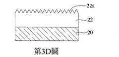
於本實施例中,移除該圖案化阻層28及形成粗糙面22a之製程係如第3A至3D圖所示。具體地,如第3A圖所示,係採用如深反應離子式蝕刻(deep reactive ion etching,簡稱DRIE)之第一方式轟擊Y(如實線箭頭方向)該圖案化阻層28,使該圖案化阻層38表面粗糙化,且由於光阻材質對於DRIE較敏感,故可產生高低差大之粗糙度。接著,如第3B至3C圖所示,係採用如電漿(DESCUM)之第二方式轟擊X(如虛線箭頭方向)已表面粗糙化之圖案化阻層38’,且持續轟擊至該圖案化阻層38”即將消失。之後,如第3D圖所示,轟擊到該圖案化阻層38”完全移除,且持續電漿轟擊該絕緣層22,使該絕緣層22產生粗糙面22a,且該粗糙面22a具有高低差大之粗糙度,例如,該粗糙面22a之粗糙度大於20埃米且小於100埃米(尤其是30至70埃米),較佳者,該粗糙面22a之粗糙度可為49.6埃米,其中,1奈米(nm)等於10埃米(À)。In this embodiment, the processes of removing the patterned resist
需注意,因該絕緣層22對DRIE之敏感性小,故不可一直使用DRIE轟擊該圖案化阻層28及該絕緣層22,否則即使該圖案化阻層28被DRIE轟擊消失,該絕緣層22受該DRIE轟擊仍無法產生高低差大之粗糙面。It should be noted that because the sensitivity of the insulating
另外,若該絕緣層22上未覆蓋已粗糙化之圖案化阻層38,38’,38”,而以電漿直接轟擊該絕緣層22,該絕緣層22之粗糙面22a之粗糙度將小於10埃米,即使增長電漿轟擊時間,亦僅使該絕緣層22之厚度變薄,而該粗糙面22a之粗糙度仍小於10埃米。In addition, if the insulating
本發明之製法係利用電漿等向性製程特性會因前道製程產生的形貌差異而使電漿對表面轟擊時間產生差異,進而將該圖案化阻層28的表面形貌複印於該絕緣層22上,以達到有效控制該絕緣層22之粗糙面22a之粗糙度,且能得到較高之表面粗糙度。因此,於後續製程中,若將該基板結構2應用於封裝製程,當產生應力變化時,該絕緣層22之粗糙面22a不僅可增強該基板結構2與底膠之結合性,且能分散應力而避免應力集中於該基板結構2之角落,以有效防止該基板結構2發生破裂,故相較於習知技術,本發明之基板結構2能避免與底膠之間發生脫層問題,因而能提升產品可靠度,且能有效使用於終端產品。The manufacturing method of the present invention utilizes the isotropic process characteristics of plasma to cause the difference in the bombardment time of the plasma to the surface due to the difference in morphology produced by the previous process,Furthermore, the surface morphology of the patterned resist
再者,由於該圖案化阻層28係用於製作該導電元件27,故無需額外增加製程即可同時製作該絕緣層22之粗糙面22a,因而能有效降低生產成本。Furthermore, since the patterned resist
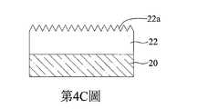
又,可依需求調整該絕緣層之粗糙面之特徵。例如,改變該圖案化阻層之粗糙深度,如第4A至4C圖所示,先以深反應離子式蝕刻(DRIE)Y(如實線箭頭方向)之轟擊方式調整圖案化阻層28具較小粗糙化深度t,及如第4A’至4C’圖所示,以深反應離子式蝕刻(DRIE)Y(如實線箭頭方向)之轟擊方式調整圖案化阻層48具較大粗糙化深度h,再進行電漿轟擊作業X(如虛線箭頭方向),以使絕緣層22具有不同粗糙化深度之粗糙面22a,42a。或者,改變高低差間距密度,如第5A至5C圖所示之圖案化阻層28具有較大密度之凹凸狀及如第5A’至5C’圖所示之圖案化阻層58具有較小密度之凹凸狀,再進行電漿轟擊作業X(如虛線箭頭方向),以使絕緣層22具有不同高低差間距密度之粗糙面22a,52a。亦或,改變該圖案化阻層28,68圖案,如第6A至6C圖所示之圖案化阻層28具有粗糙部682、凹部680及如第6A’至6C’圖所示之圖案化阻層68具有貫穿孔681,再進行電漿轟擊作業X(如虛線箭頭方向),以使絕緣層22具有不同圖案之粗糙面22a,62a。Moreover, the characteristics of the rough surface of the insulating layer can be adjusted according to requirements. For example, to change the roughness depth of the patterned resist layer, as shown in FIGS. 4A to 4C, first adjust the patterned resist
另外,同一粗糙面可形成有不同之粗糙度,如第6C圖所示之粗糙面22a、或第6C’圖所示之粗糙面62a。In addition, different roughnesses may be formed on the same rough surface, such as the
本發明復提供一種基板結構2,係包括:一基板本體20、以及形成於該基板本體20上且具有粗糙面22a,42a,52a,62a之絕緣層22,42,52,62,其中,該粗糙面22a,42a,52a,62a之粗糙度係大於20埃米。The present invention further provides a
於一實施例中,該基板本體20係具有至少一電性接點200。進一步,該絕緣層22形成有對應該電性接點200之開孔220,且該電性接點200上接觸形成有金屬層26,並可包括形成於該電性接點200上之導電元件27。In one embodiment, the
於一實施例中,粗糙面22a,42a,52a,62a之粗糙度係小於100埃米,例如,該粗糙面22a,42a,52a,62a之粗糙度係為30至70埃米;較佳者,該粗糙面22a,42a,52a,62a之粗糙度係為49.6埃米。In one embodiment, the roughness of the
於一實施例中,該粗糙面62a係具有不同之粗糙度。In one embodiment, the
綜上所述,本發明之基板結構及其製法,係藉由形成圖案化阻層於絕緣層上,並於移除該圖案化阻層時,同時粗糙化該圖案化阻層及絕緣層,以將該圖案化阻層的表面形貌複印於該絕緣層上,進而使該絕緣層與該圖案化阻層之接觸面產生粗糙面,故於後續封裝製程中,該絕緣層之粗糙面不僅能增強該基板結構與膠材之結合性,且能分散應力以防止該基板結構發生破裂,因而能避免該基板結構與膠材之間發生脫層問題。In summary, the substrate structure and the manufacturing method of the present invention, by forming a patterned resist layer on the insulating layer, and roughening the patterned resist layer and the insulating layer simultaneously when removing the patterned resist layer, To copy the surface morphology of the patterned resist layer on the insulating layer, so that the insulating layer and the patterned resist layerThe contact surface produces a rough surface, so in the subsequent packaging process, the rough surface of the insulating layer can not only enhance the bonding between the substrate structure and the adhesive, but also can disperse the stress to prevent the substrate structure from cracking, thus avoiding the substrate A delamination problem occurs between the structure and the glue.
上述實施例係用以例示性說明本發明之原理及其功效,而非用於限制本發明。任何熟習此項技藝之人士均可在不違背本發明之精神及範疇下,對上述實施例進行修改。因此本發明之權利保護範圍,應如後述之申請專利範圍所列。The above embodiments are used to exemplify the principles and effects of the present invention, rather than to limit the present invention. Anyone who is familiar with this skill can modify the above embodiments without departing from the spirit and scope of the present invention. Therefore, the scope of protection of the rights of the present invention should be as listed in the scope of patent application mentioned later.
2‧‧‧基板結構2‧‧‧Substrate structure
20‧‧‧基板本體20‧‧‧Substrate body
200‧‧‧電性接點200‧‧‧Electrical contact
22‧‧‧絕緣層22‧‧‧Insulation
22a‧‧‧粗糙面22a‧‧‧Rough
25‧‧‧絕緣保護層25‧‧‧Insulation protective layer
26‧‧‧金屬層26‧‧‧Metal layer
27‧‧‧導電元件27‧‧‧Conducting element
Claims (17)
Translated fromChinesePriority Applications (2)
| Application Number | Priority Date | Filing Date | Title |
|---|---|---|---|
| TW106117021ATWI683407B (en) | 2017-05-23 | 2017-05-23 | Substrate structure and method for fabricating the same |
| CN201710473882.7ACN108962869B (en) | 2017-05-23 | 2017-06-21 | Substrate structure and method for fabricating the same |
Applications Claiming Priority (1)
| Application Number | Priority Date | Filing Date | Title |
|---|---|---|---|
| TW106117021ATWI683407B (en) | 2017-05-23 | 2017-05-23 | Substrate structure and method for fabricating the same |
Publications (2)
| Publication Number | Publication Date |
|---|---|
| TW201901900A TW201901900A (en) | 2019-01-01 |
| TWI683407Btrue TWI683407B (en) | 2020-01-21 |
Family
ID=64495054
Family Applications (1)
| Application Number | Title | Priority Date | Filing Date |
|---|---|---|---|
| TW106117021ATWI683407B (en) | 2017-05-23 | 2017-05-23 | Substrate structure and method for fabricating the same |
Country Status (2)
| Country | Link |
|---|---|
| CN (1) | CN108962869B (en) |
| TW (1) | TWI683407B (en) |
Citations (5)
| Publication number | Priority date | Publication date | Assignee | Title |
|---|---|---|---|---|
| US20040099959A1 (en)* | 2002-11-22 | 2004-05-27 | Hannstar Display Corp. | Conductive bump structure |
| TW200725765A (en)* | 2005-12-20 | 2007-07-01 | Fujitsu Ltd | Semiconductor device and manufacturing method of the same |
| TW201225220A (en)* | 2010-12-13 | 2012-06-16 | Taiwan Semiconductor Mfg | Method for manufacturing microelectronic device and integrated circuit to prevent metal pad damage in wafer level package |
| TW201419393A (en)* | 2012-11-14 | 2014-05-16 | Advanced Semiconductor Eng | Method for dicing a semiconductor wafer having through silicon vias and resultant structures |
| TW201542049A (en)* | 2014-04-16 | 2015-11-01 | 矽品精密工業股份有限公司 | Substrate with electrical interconnector structure and manufacturing method thereof |
Family Cites Families (9)
| Publication number | Priority date | Publication date | Assignee | Title |
|---|---|---|---|---|
| JP2776886B2 (en)* | 1989-05-31 | 1998-07-16 | イビデン株式会社 | Multilayer printed wiring board and method of manufacturing the same |
| JPH0983138A (en)* | 1995-09-07 | 1997-03-28 | Nippon Polytec Kk | Method of manufacturing multi-layered printed wiring board |
| KR20120104641A (en)* | 2004-02-04 | 2012-09-21 | 이비덴 가부시키가이샤 | Multilayer printed wiring board |
| JP2006222232A (en)* | 2005-02-09 | 2006-08-24 | Fujitsu Ltd | Semiconductor device and manufacturing method thereof |
| US7462784B2 (en)* | 2006-05-02 | 2008-12-09 | Ibiden Co., Ltd. | Heat resistant substrate incorporated circuit wiring board |
| US7659632B2 (en)* | 2006-11-03 | 2010-02-09 | Taiwan Seminconductor Manufacturing Co., Ltd. | Solder bump structure and method of manufacturing same |
| US8629053B2 (en)* | 2010-06-18 | 2014-01-14 | Taiwan Semiconductor Manufacturing Company, Ltd. | Plasma treatment for semiconductor devices |
| US10163828B2 (en)* | 2013-11-18 | 2018-12-25 | Taiwan Semiconductor Manufacturing Company Ltd. | Semiconductor device and fabricating method thereof |
| KR101683975B1 (en)* | 2014-08-05 | 2016-12-07 | 앰코 테크놀로지 코리아 주식회사 | Semiconducotr device, semiconductor package and metode for manufacturing thereof |
- 2017
- 2017-05-23TWTW106117021Apatent/TWI683407B/enactive
- 2017-06-21CNCN201710473882.7Apatent/CN108962869B/enactiveActive
Patent Citations (5)
| Publication number | Priority date | Publication date | Assignee | Title |
|---|---|---|---|---|
| US20040099959A1 (en)* | 2002-11-22 | 2004-05-27 | Hannstar Display Corp. | Conductive bump structure |
| TW200725765A (en)* | 2005-12-20 | 2007-07-01 | Fujitsu Ltd | Semiconductor device and manufacturing method of the same |
| TW201225220A (en)* | 2010-12-13 | 2012-06-16 | Taiwan Semiconductor Mfg | Method for manufacturing microelectronic device and integrated circuit to prevent metal pad damage in wafer level package |
| TW201419393A (en)* | 2012-11-14 | 2014-05-16 | Advanced Semiconductor Eng | Method for dicing a semiconductor wafer having through silicon vias and resultant structures |
| TW201542049A (en)* | 2014-04-16 | 2015-11-01 | 矽品精密工業股份有限公司 | Substrate with electrical interconnector structure and manufacturing method thereof |
Also Published As
| Publication number | Publication date |
|---|---|
| CN108962869A (en) | 2018-12-07 |
| TW201901900A (en) | 2019-01-01 |
| CN108962869B (en) | 2022-07-05 |
Similar Documents
| Publication | Publication Date | Title |
|---|---|---|
| TWI640045B (en) | Semiconductor device and method of manufacture | |
| CN106952884B (en) | Fan-out wafer grade encapsulates | |
| TW201913928A (en) | Semiconductor component package and method of manufacturing same | |
| TW201724380A (en) | Electronic package and substrate for packaging use | |
| TWI543323B (en) | Interposer and method of manufacture | |
| KR20210148846A (en) | Semiconductor device and method of manufacture | |
| US11114308B2 (en) | Controlling of height of high-density interconnection structure on substrate | |
| CN104956479A (en) | Integrated circuit package with offset vias | |
| CN106486384A (en) | Method for manufacturing wafer level package | |
| CN113675163B (en) | Semiconductor device and method for manufacturing the same | |
| TW202301603A (en) | Package structures | |
| TWI601259B (en) | Electronic package, semiconductor substrate of the electronic package, and method for manufacturing the electronic package | |
| CN113314505A (en) | Semiconductor package and method of manufacturing the same | |
| TWI651819B (en) | Substrate structure and its preparation method | |
| TWI719670B (en) | Integrated circuit package and method of manufacturing the same | |
| TWI641094B (en) | Substrate structure and method of manufacture | |
| TWI669793B (en) | Substrate structure | |
| KR20230006531A (en) | Bump-free superconductor device | |
| TWI821476B (en) | Semiconductor device and manufacturing method thereof | |
| TWI683407B (en) | Substrate structure and method for fabricating the same | |
| TWI614862B (en) | Substrate structure and the manufacture thereof | |
| TW202349596A (en) | Semiconductor package | |
| TWI705547B (en) | Chip package structure and manufacturing method thereof | |
| KR102473590B1 (en) | Semiconductor device and method | |
| TWI821960B (en) | Package structure and method for forming the same |