TWI683291B - Display device and manufacturing method thereof - Google Patents
Display device and manufacturing method thereofDownload PDFInfo
- Publication number
- TWI683291B TWI683291BTW107132819ATW107132819ATWI683291BTW I683291 BTWI683291 BTW I683291BTW 107132819 ATW107132819 ATW 107132819ATW 107132819 ATW107132819 ATW 107132819ATW I683291 BTWI683291 BTW I683291B
- Authority
- TW
- Taiwan
- Prior art keywords
- spacer
- mold
- housing
- display device
- display element
- Prior art date
Links
- 238000004519manufacturing processMethods0.000titleclaimsabstractdescription14
- 125000006850spacer groupChemical group0.000claimsabstractdescription89
- 239000006260foamSubstances0.000claimsdescription17
- 238000000034methodMethods0.000claimsdescription11
- 238000003825pressingMethods0.000claimsdescription8
- 238000004891communicationMethods0.000claimsdescription5
- 239000000463materialSubstances0.000claimsdescription4
- 239000011261inert gasSubstances0.000claimsdescription2
- 239000004033plasticSubstances0.000claimsdescription2
- 229920001296polysiloxanePolymers0.000claimsdescription2
- 238000010438heat treatmentMethods0.000claims1
- 238000013461designMethods0.000description8
- 239000004973liquid crystal related substanceSubstances0.000description4
- 230000000694effectsEffects0.000description3
- 238000001125extrusionMethods0.000description3
- 230000003139buffering effectEffects0.000description2
- 239000000084colloidal systemSubstances0.000description2
- 238000010586diagramMethods0.000description2
- 230000005489elastic deformationEffects0.000description2
- 239000007789gasSubstances0.000description2
- 239000007788liquidSubstances0.000description2
- 238000013459approachMethods0.000description1
- 239000011248coating agentSubstances0.000description1
- 238000000576coating methodMethods0.000description1
- 238000011161developmentMethods0.000description1
- 238000009826distributionMethods0.000description1
- 239000006261foam materialSubstances0.000description1
- 239000003292glueSubstances0.000description1
- 238000009434installationMethods0.000description1
- 230000010354integrationEffects0.000description1
- 238000012986modificationMethods0.000description1
- 230000004048modificationEffects0.000description1
- 238000003466weldingMethods0.000description1
Images


Landscapes
- Liquid Crystal (AREA)
- Devices For Indicating Variable Information By Combining Individual Elements (AREA)
Abstract
Description
Translated fromChinese本發明是有關於一種顯示裝置,且特別是有關於一種顯示裝置及其製作方法。The present invention relates to a display device, and more particularly to a display device and a manufacturing method thereof.
因應消費者的使用需求,輕薄化設計已成為現有多數電子產品的發展趨勢。以顯示裝置為例,現有顯示裝置大多採用液晶顯示螢幕,惟液晶顯示螢幕的結構強度較為不足,容易因碰撞或擠壓而損傷。In response to consumer demand, thin and light design has become the development trend of most existing electronic products. Taking the display device as an example, most of the existing display devices use a liquid crystal display screen, but the structure strength of the liquid crystal display screen is relatively insufficient, and it is easy to be damaged due to collision or extrusion.
為滿足輕薄化的設計需求,用以與液晶顯示螢幕整合的殼體常選用密度較低且結構強度較弱的材料製作,或者是選用結構強度較佳的材料製作,但減薄殼體的厚度。上述作法皆會削減殼體保護液晶顯示螢幕的效果。另一常見的作法是讓殼體與液晶顯示螢幕之間留有間隙,避免殼體受力變形時碰撞或擠壓液晶顯示螢幕。然而,這樣的作法並無法符合輕薄化的設計需求,並且,當殼體所產生的變形量較大時,仍難避免液晶顯示螢幕受殼體碰撞或擠壓。In order to meet the design requirements of thinness and thinness, the casing used for integration with the LCD screen is often made of a material with a lower density and a weaker structural strength, or a material with a better structural strength, but the thickness of the casing is reduced . All of the above methods will reduce the effect of the housing to protect the LCD screen. Another common practice is to leave a gap between the casing and the LCD screen to avoid collision or squeezing of the LCD screen when the casing is deformed by force. However, such an approach cannot meet the design requirements of thinness and thinness, and when the amount of deformation generated by the housing is large, it is still difficult to avoid the liquid crystal display screen from being hit or squeezed by the housing.
本發明提供一種顯示裝置,其具有良好的可靠度。The present invention provides a display device with good reliability.
本發明提供一種上述顯示裝置的製作方法。The invention provides a method for manufacturing the above display device.
本發明提出一種顯示裝置,其包括殼體、間隔件以及顯示元件。間隔件設置於殼體內,其中間隔件具有第一表面、相對於第一表面的第二表面以及位於第一表面與第二表面之間的腔室,且第一表面抵接殼體。顯示元件設置於殼體內,且抵接間隔件的第二表面。The present invention provides a display device including a housing, a spacer, and a display element. The spacer is disposed in the housing, wherein the spacer has a first surface, a second surface opposite to the first surface, and a cavity between the first surface and the second surface, and the first surface abuts the housing. The display element is disposed in the housing and abuts the second surface of the spacer.
本發明提出一種顯示裝置的製作方法,其包括下列步驟。首先,將殼體置入第一模具。在殼體內形成發泡層。接著,將第二模具與第一模具結合,且殼體與發泡層位於第一模具與第二模具之間。然後,使發泡層膨脹變形以成形間隔件。接著,將第二模具與第一模具分離以暴露出間隔件。之後,將顯示元件置入殼體,並使顯示元件抵接間隔件。The invention provides a method for manufacturing a display device, which includes the following steps. First, place the housing into the first mold. A foam layer is formed in the casing. Next, the second mold and the first mold are combined, and the shell and the foam layer are located between the first mold and the second mold. Then, the foam layer is expanded and deformed to form a spacer. Next, the second mold is separated from the first mold to expose the spacer. After that, the display element is placed into the housing, and the display element is brought into contact with the spacer.
基於上述,藉由將間隔件設置於殼體與顯示元件之間,當外力作用於殼體時,間隔件可起緩衝的效果,避免顯示元件受殼體碰撞或擠壓而損傷。因此,本發明的顯示裝置具有良好的可靠度。另外,本發明所提出的上述顯示裝置的製作方法可獲致良好的製程良率。Based on the above, by placing the spacer between the casing and the display element, when an external force acts on the casing, the spacer can serve as a buffering effect to prevent the display element from being damaged by collision or extrusion of the casing. Therefore, the display device of the present invention has good reliability. In addition, the manufacturing method of the above display device proposed by the present invention can achieve good process yield.
為讓本發明的上述特徵和優點能更明顯易懂,下文特舉實施例,並配合所附圖式作詳細說明如下。In order to make the above-mentioned features and advantages of the present invention more obvious and understandable, the embodiments are specifically described below in conjunction with the accompanying drawings for detailed description as follows.
圖1是本發明第一實施例的顯示裝置的剖面示意圖。圖2是本發明第一實施例的間隔件的俯視示意圖。為清楚表示與便於說明,圖2省略繪示逆止閥140。請參考圖1與圖2,在本實施例中,顯示裝置100包括殼體110、間隔件120以及顯示元件130,其中殼體110用以收容間隔件120與顯示元件130,且間隔件120用以分隔顯示元件130與殼體110,避免顯示元件130與殼體110直接接觸。舉例來說,顯示元件130可為液晶面板與背光模組的組合,且可選擇整合有觸控功能。另一方面,間隔件120可採用塑膠、矽膠、橡膠、發泡材或其他具有良好的緩衝效果的材質製作而成,因此,當外力作用於殼體110時,間隔件120可起緩衝的效果,避免顯示元件130受殼體100碰撞或擠壓而損傷。基於間隔件120的設置,殼體100的厚度可適度減薄,故本實施例的顯示裝置100不僅能符合輕薄化的設計需求,也能具有良好的可靠度。FIG. 1 is a schematic cross-sectional view of a display device according to a first embodiment of the invention. FIG. 2 is a schematic top view of the spacer of the first embodiment of the present invention. For clarity and ease of description, the
間隔件120與顯示元件130皆設置於殼體110內,其中間隔件120具有第一表面121、相對於第一表面121的第二表面122以及位於第一表面121與第二表面122之間的腔室123,且間隔件120係以第一表面121抵接殼體110朝向顯示元件130的內面111。另一方面,間隔件120係以第二表面122抵接顯示元件130朝向殼體110的內面131。舉例來說,間隔件120的第二表面122可以是完全覆蓋顯示元件130的內面131,但不限於此。在其他實施例中,間隔件的第二表面可以是局部覆蓋顯示元件朝向殼體的內面,例如覆蓋顯示元件朝向殼體的內面的至少50%,惟此覆蓋比例可視實際而調整,且間隔件的所在位置盡可能落在整體裝置的中央,但不限於此。The
在本實施例中,間隔件120被夾持於顯示元件130的內面131與殼體110的內面111之間,舉例來說,間隔件120可藉由顯示元件130與殼體110的夾持力固定於顯示元件130的內面131與殼體110的內面111之間,或者是藉由膠體黏貼固定於顯示元件130的內面131與殼體110的內面111,又或者是間隔件120直接製作成型於殼體110的內面111。另一方面,在間隔件120的旁側可選擇設置膠體(未繪示),並使膠體(未繪示)的兩端接合顯示元件130的內面131與殼體110的內面111。基於上述設計,有助於防止顯示裝置100的各構件受外力的作用而相對移動。In this embodiment, the
另一方面,間隔件120內部設有腔室123,此處,腔室123的所在位置盡可能落在整體裝置的中央,並向四周延伸,但不限於此。由於間隔件120具有彈性變形裕度,且內部設有中空腔室,因此作用於殼體110的外力得以被分散。在本實施例中,顯示裝置100更包括逆止閥140,穿設於間隔件120的一側,且延伸至腔室123。基於逆止閥140的設置,可注入氣體或液體以調整腔室123的體積大小,並防止腔室123內的氣體或液體外洩。在其他實施例中,間隔件的腔室可為密閉空間,未設有逆止閥、其他類型的連通閥或貫孔與外界連通。On the other hand, a
此外,顯示裝置100更包括框架150,設置於殼體110上,且壓抵顯示元件130的邊緣。進一步來說,框架150包括壓抵部151與連接壓抵部151的卡合部152,其中壓抵部151用以將顯示元件130,壓抵於壓抵部151與間隔件120之間。此外,卡合部152自顯示元件130的一側穿入殼體110,並與殼體110的內壁面112相卡合。其中,內壁面112連接內面111。舉例來說,卡合部152可設有卡勾,而殼體110的內壁面112則對應設有卡槽,或者是,卡合部152可設有卡槽,而殼體110的內壁面112則對應設有卡勾。在其他實施例中,可採用其他方式將框架固定於殼體,例如鎖附、焊接、鉚接或黏貼等方式。In addition, the
特別說明的是,本實施例的殼體110的內面111為平面,在其他實施例中,殼體朝向顯示元件的內面可為凸面或弧面,並凸向間隔件。In particular, the
以下將列舉其他實施例以作為說明。在此必須說明的是,下述實施例沿用前述實施例的元件標號與部分內容,其中採用相同的標號來表示相同或近似的元件,並且省略了相同技術內容的說明。關於省略部分的說明可參考前述實施例,下述實施例不再重複贅述。The following will list other embodiments as illustrations. It must be noted here that the following embodiments follow the element numbers and partial contents of the foregoing embodiments, wherein the same reference numbers are used to indicate the same or similar elements, and the description of the same technical content is omitted. For the description of the omitted parts, reference may be made to the foregoing embodiments, and the following embodiments will not be repeated.
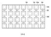
圖3是本發明第二實施例的顯示裝置的剖面示意圖。圖4是本發明第二實施例的間隔件的俯視示意圖。請參考圖3及圖4,本實施例的顯示裝置100A與第一實施例的顯示裝置100略有不同,主要差異在於:間隔件的腔室的結構設計。進一步來說,在本實施例中,間隔件120a的腔室係由多個子腔室123a組成,其中這些子腔室123a互不連通,且平均分佈於間隔件120a。另一方面,間隔件120a具有多個凸出部124,其中這些凸出部124抵接殼體110的內面111,且這些凸出部124的數量與這些子腔室123a的數量相同。此外,每一個凸出部124正對一個子腔室123a,而間隔件120a朝向殼體110的內面111的一側未設有凸出部124的其他區域形成凹陷部126。特別說明的是,本實施例的各個子腔室123a為獨立且密閉的空間,在其他實施例中,各個子腔室可選擇逆止閥、其他類型的連通閥或貫孔與外界連通。3 is a schematic cross-sectional view of a display device according to a second embodiment of the invention. 4 is a schematic plan view of a spacer according to a second embodiment of the invention. Please refer to FIGS. 3 and 4. The
圖5是本發明第三實施例的間隔件的俯視示意圖。請參考圖5,本實施例的間隔件120b與第二實施例的間隔件120a略有不同,主要差異在於:這些子腔室的連通與否。進一步來說,在本實施例中,間隔件120b的內部設有多個子腔室123b與多個連通道125,其中任一個連通道125用以連通任二個子腔室123b。此處,部分連通道125沿縱向連通部分子腔室123b,另一部分連通道125沿橫向連通另一部分子腔室123b。FIG. 5 is a schematic top view of a spacer according to a third embodiment of the invention. Please refer to FIG. 5. The
圖6是本發明第四實施例的間隔件的俯視示意圖。請參考圖6,本實施例的間隔件120c與第三實施例的間隔件120b略有不同,主要差異在於:連通道的分佈型態。進一步來說,在本實施例中,間隔件120c的內部設有多個子腔室123c與多個連通道125,其中任一個連通道125用以沿縱向連通任二個子腔室123c,且任二相鄰的子腔室123c在橫向上未有連通。6 is a schematic plan view of a spacer according to a fourth embodiment of the invention. Please refer to FIG. 6. The
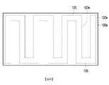
圖7是本發明第五實施例的間隔件的俯視示意圖。請參考圖7,本實施例的間隔件120d與第一實施例的間隔件120略有不同,主要差異在於:間隔件的腔室的結構設計。進一步來說,在本實施例中,間隔件120d的腔室係由多個子腔室123d組成,其中這些子腔室123d互不連通,且並列於間隔件120d。另一方面,各個子腔室123d的形狀為長條狀,並且沿縱向延伸。在其他實施例中,各個子腔室可沿橫向延伸,但不限於此。7 is a schematic plan view of a spacer according to a fifth embodiment of the invention. Please refer to FIG. 7. The
特別說明的是,本實施例的各個子腔室123d為獨立且密閉的空間,在其他實施例中,各個子腔室可選擇逆止閥、其他類型的連通閥或貫孔與外界連通。In particular, each sub-chamber 123d of this embodiment is an independent and closed space. In other embodiments, each sub-chamber can select a check valve, other type of communication valve, or a through hole to communicate with the outside world.
圖8是本發明第六實施例的間隔件的俯視示意圖。請參考圖8,本實施例的間隔件120e與第五實施例的間隔件120d略有不同,主要差異在於:這些子腔室的連通與否。進一步來說,在本實施例中,間隔件120e的內部設有多個子腔室123e與多個連通道125,其中任二相鄰的子腔室123e透過一個連通道125相連通,且此連通道125沿橫向延伸。8 is a schematic plan view of a spacer according to a sixth embodiment of the invention. Referring to FIG. 8, the
基於上述實施例所揭,當可實際需求組合各實施例的腔式的結構型態、調整腔室的數量或調整各腔室間的連通關係,並整合於顯示裝置中。Based on the disclosure of the above-mentioned embodiments, when the actual requirements can combine the structural types of the chambers of the embodiments, adjust the number of chambers or adjust the communication relationship between the chambers, and integrate them into the display device.
圖9至圖12是本發明一實施例的顯示裝置的製作流程示意圖。若採用發泡材製作間隔件,則顯示裝置的製作流程大致如下:首先,請參考圖9,將殼體110置入第一模具210,其中第一模具210例如是母模,且具有用以收容殼體110的凹穴211。接著,採塗佈、印刷或其他適用方法在殼體110的內面111上形成發泡層127。然後,進行合模的步驟,也就是將第二模具220與第一模具210結合,其中第二模具220例如是公模,且具有用以伸入凹穴211的凸部221。在合模後,殼體110與發泡層127位於第一模具210與第二模具220之間,且第二模具220的凸部221進一步伸入殼體110,但與發泡層127保持距離,如圖10所示。9 to 12 are schematic diagrams of a manufacturing process of a display device according to an embodiment of the invention. If the spacer is made of foam material, the manufacturing process of the display device is roughly as follows: First, please refer to FIG. 9, the
接著,請參考圖11,加熱發泡層127或注入惰性氣體至第一模具210與第二模具220之間,使發泡層127膨脹變形以成形間隔件128。因第二模具220的凸部221伸入殼體110,發泡層127會在抵觸第二模具220的凸部221後停止向上膨脹變形。也就是說,第二模具220能用以限制發泡層127的膨脹高度,以避免製作所得的間隔件128超出殼體110外而對顯示元件130的安裝造成阻礙。之後,請參考圖12,將第二模具220與第一模具210分離以暴露出間隔件128。後續,將顯示元件130置入殼體110,並使顯示元件130抵接間隔件128。Next, referring to FIG. 11, the
在製作間隔件128的過程中,已對顯示元件130的高度(或稱厚度)進行考量,避免置放於間隔件128上的顯示元件130的局部超出殼體外110,以提高製程良率。特別說明的是,在上述製作步驟後,可進一步採用框架壓抵顯示元件的邊緣,並將框架固定於與殼體。In the process of manufacturing the
綜上所述,藉由將間隔件設置於殼體與顯示元件之間,當外力作用於殼體時,間隔件可起緩衝的效果,避免顯示元件受殼體碰撞或擠壓而損傷。此外,間隔件具有彈性變形裕度,且內部設有中空腔室,故能分散作用於殼體的外力。因此,本發明的顯示裝置不僅能符合輕薄化的設計需求,也能具有良好的可靠度。另外,本發明所提出的上述顯示裝置的製作方法可獲致良好的製程良率。In summary, by placing the spacer between the casing and the display element, when an external force acts on the casing, the spacer can serve as a buffering effect to prevent the display element from being damaged by collision or extrusion of the casing. In addition, the spacer has an elastic deformation margin, and a hollow cavity is provided inside, so that the external force acting on the housing can be dispersed. Therefore, the display device of the present invention can not only meet the design requirements of lightness and thinness, but also have good reliability. In addition, the manufacturing method of the above display device proposed by the present invention can achieve good process yield.
雖然本發明已以實施例揭露如上,然其並非用以限定本發明,任何所屬技術領域中具有通常知識者,在不脫離本發明的精神和範圍內,當可作些許的更動與潤飾,故本發明的保護範圍當視後附的申請專利範圍所界定者為準。Although the present invention has been disclosed as above with examples, it is not intended to limit the present invention. Any person with ordinary knowledge in the technical field can make some changes and modifications without departing from the spirit and scope of the present invention. The scope of protection of the present invention shall be subject to the scope defined in the appended patent application.
100、100A‧‧‧顯示裝置100、100A‧‧‧Display device
110‧‧‧殼體110‧‧‧Housing
111、131‧‧‧內面111、131‧‧‧Inside
112‧‧‧內壁面112‧‧‧Inner wall
120、120a~120e、128‧‧‧間隔件120, 120a~120e, 128‧‧‧ spacer
121‧‧‧第一表面121‧‧‧First surface
122‧‧‧第二表面122‧‧‧Second surface
123‧‧‧腔室123‧‧‧ chamber
123a~123e‧‧‧子腔室123a~123e‧‧‧Sub chamber
124‧‧‧凸出部124‧‧‧Projection
125、125a‧‧‧連通道125, 125a‧‧‧ connected channel
126‧‧‧凹陷部126‧‧‧Depression
127‧‧‧發泡層127‧‧‧foam layer
130‧‧‧顯示元件130‧‧‧Display element
140‧‧‧逆止閥140‧‧‧Check valve
150‧‧‧框架150‧‧‧frame
151‧‧‧抵壓部151‧‧‧Pressure Department
152‧‧‧卡合部152‧‧‧Joint Department
210‧‧‧第一模具210‧‧‧ First mold
211‧‧‧凹穴211‧‧‧Cavities
220‧‧‧第二模具220‧‧‧Second mould
221‧‧‧凸部221‧‧‧Convex
圖1是本發明第一實施例的顯示裝置的剖面示意圖。 圖2是本發明第一實施例的間隔件的俯視示意圖。 圖3是本發明第二實施例的顯示裝置的剖面示意圖。 圖4是本發明第二實施例的間隔件的俯視示意圖。 圖5是本發明第三實施例的間隔件的俯視示意圖。 圖6是本發明第四實施例的間隔件的俯視示意圖。 圖7是本發明第五實施例的間隔件的俯視示意圖。 圖8是本發明第六實施例的間隔件的俯視示意圖。 圖9至圖12是本發明一實施例的顯示裝置的製作流程示意圖。FIG. 1 is a schematic cross-sectional view of a display device according to a first embodiment of the invention. FIG. 2 is a schematic top view of the spacer of the first embodiment of the present invention. 3 is a schematic cross-sectional view of a display device according to a second embodiment of the invention. 4 is a schematic plan view of a spacer according to a second embodiment of the invention. FIG. 5 is a schematic top view of a spacer according to a third embodiment of the invention. 6 is a schematic plan view of a spacer according to a fourth embodiment of the invention. 7 is a schematic plan view of a spacer according to a fifth embodiment of the invention. 8 is a schematic plan view of a spacer according to a sixth embodiment of the invention. 9 to 12 are schematic diagrams of a manufacturing process of a display device according to an embodiment of the invention.
100‧‧‧顯示裝置100‧‧‧Display device
110‧‧‧殼體110‧‧‧Housing
111、131‧‧‧內面111、131‧‧‧Inside
112‧‧‧內壁面112‧‧‧Inner wall
120‧‧‧間隔件120‧‧‧ spacer
121‧‧‧第一表面121‧‧‧First surface
122‧‧‧第二表面122‧‧‧Second surface
123‧‧‧腔室123‧‧‧ chamber
130‧‧‧顯示元件130‧‧‧Display element
140‧‧‧逆止閥140‧‧‧Check valve
150‧‧‧框架150‧‧‧frame
151‧‧‧抵壓部151‧‧‧Pressure Department
152‧‧‧卡合部152‧‧‧Joint Department
Claims (8)
Translated fromChinesePriority Applications (1)
| Application Number | Priority Date | Filing Date | Title |
|---|---|---|---|
| TW107132819ATWI683291B (en) | 2018-09-18 | 2018-09-18 | Display device and manufacturing method thereof |
Applications Claiming Priority (1)
| Application Number | Priority Date | Filing Date | Title |
|---|---|---|---|
| TW107132819ATWI683291B (en) | 2018-09-18 | 2018-09-18 | Display device and manufacturing method thereof |
Publications (2)
| Publication Number | Publication Date |
|---|---|
| TWI683291Btrue TWI683291B (en) | 2020-01-21 |
| TW202013333A TW202013333A (en) | 2020-04-01 |
Family
ID=69942601
Family Applications (1)
| Application Number | Title | Priority Date | Filing Date |
|---|---|---|---|
| TW107132819ATWI683291B (en) | 2018-09-18 | 2018-09-18 | Display device and manufacturing method thereof |
Country Status (1)
| Country | Link |
|---|---|
| TW (1) | TWI683291B (en) |
Citations (7)
| Publication number | Priority date | Publication date | Assignee | Title |
|---|---|---|---|---|
| TWM413137U (en)* | 2011-02-21 | 2011-10-01 | Chunghwa Picture Tubes Ltd | Display panel |
| TWM421511U (en)* | 2011-07-28 | 2012-01-21 | Chunghwa Picture Tubes Ltd | Buffer member and display device |
| CN102494273A (en)* | 2011-11-29 | 2012-06-13 | 深圳市华星光电技术有限公司 | Backlight module and liquid crystal display device |
| TW201333585A (en)* | 2012-02-13 | 2013-08-16 | Briview Corp | Display device with frame configuration |
| TW201607403A (en)* | 2014-08-04 | 2016-02-16 | 佳世達科技股份有限公司 | Fixing structure for fixing a frame and a display module and display device therewith |
| US20170160580A1 (en)* | 2015-12-04 | 2017-06-08 | Samsung Display Co., Ltd. | Curved display device and method for manufacturing the same |
| TW201818206A (en)* | 2016-11-02 | 2018-05-16 | 友達光電股份有限公司 | Touch display device |
- 2018
- 2018-09-18TWTW107132819Apatent/TWI683291B/enactive
Patent Citations (7)
| Publication number | Priority date | Publication date | Assignee | Title |
|---|---|---|---|---|
| TWM413137U (en)* | 2011-02-21 | 2011-10-01 | Chunghwa Picture Tubes Ltd | Display panel |
| TWM421511U (en)* | 2011-07-28 | 2012-01-21 | Chunghwa Picture Tubes Ltd | Buffer member and display device |
| CN102494273A (en)* | 2011-11-29 | 2012-06-13 | 深圳市华星光电技术有限公司 | Backlight module and liquid crystal display device |
| TW201333585A (en)* | 2012-02-13 | 2013-08-16 | Briview Corp | Display device with frame configuration |
| TW201607403A (en)* | 2014-08-04 | 2016-02-16 | 佳世達科技股份有限公司 | Fixing structure for fixing a frame and a display module and display device therewith |
| US20170160580A1 (en)* | 2015-12-04 | 2017-06-08 | Samsung Display Co., Ltd. | Curved display device and method for manufacturing the same |
| TW201818206A (en)* | 2016-11-02 | 2018-05-16 | 友達光電股份有限公司 | Touch display device |
Also Published As
| Publication number | Publication date |
|---|---|
| TW202013333A (en) | 2020-04-01 |
Similar Documents
| Publication | Publication Date | Title |
|---|---|---|
| CN106585045B (en) | Mobile phone cover plate attaching mold and process thereof | |
| CN108016655B (en) | A mobile phone cover plate laminating mold and process thereof | |
| CN109448542B (en) | Display screen cover plate and display screen with same | |
| CN110827690A (en) | Laminating device | |
| CN101808486A (en) | Waterproof case and electronic device | |
| CN106062911A (en) | Waterproof key structure and waterproof mobile phone utilizing same | |
| CN101379603A (en) | Contact-bonding device | |
| JP5126219B2 (en) | Semiconductor component and method for manufacturing semiconductor component | |
| WO2022262666A1 (en) | Electronic device | |
| JP6768822B2 (en) | Gasket and its manufacturing method | |
| CN106954146A (en) | Silica gel vibrating diaphragm package assembly and preparation method for loudspeaker | |
| US7355278B2 (en) | Mold die for a semiconductor device | |
| TWI683291B (en) | Display device and manufacturing method thereof | |
| US8081290B2 (en) | Liquid crystal display panel manufacturing method and device | |
| CN110956903B (en) | Display device and method of making the same | |
| CN216287335U (en) | Terminal device | |
| CN101060016B (en) | Display device, display panel frame used therefor, and manufacturing method thereof | |
| CN102076191B (en) | Foot pad structure | |
| CN115424532A (en) | Display Modules and Electronics | |
| CN107896462A (en) | Housing and preparation method thereof, mobile terminal | |
| CN107222817B (en) | Speaker module housing and speaker module | |
| TWI704542B (en) | Display device | |
| CN210026086U (en) | Silicone Bonding Mold | |
| KR102676697B1 (en) | Lamination device | |
| CN207530906U (en) | A kind of terminal |