TWI682547B - Semiconductor structure and manufacturing method thereof - Google Patents
Semiconductor structure and manufacturing method thereofDownload PDFInfo
- Publication number
- TWI682547B TWI682547BTW104132809ATW104132809ATWI682547BTW I682547 BTWI682547 BTW I682547BTW 104132809 ATW104132809 ATW 104132809ATW 104132809 ATW104132809 ATW 104132809ATW I682547 BTWI682547 BTW I682547B
- Authority
- TW
- Taiwan
- Prior art keywords
- oxide
- layer
- containing layer
- epitaxial region
- metal
- Prior art date
Links
- 239000004065semiconductorSubstances0.000titleclaimsabstractdescription65
- 238000004519manufacturing processMethods0.000titleclaimsabstractdescription28
- 229910021332silicideInorganic materials0.000claimsabstractdescription40
- FVBUAEGBCNSCDD-UHFFFAOYSA-Nsilicide(4-)Chemical compound[Si-4]FVBUAEGBCNSCDD-UHFFFAOYSA-N0.000claimsabstractdescription40
- 239000000758substrateSubstances0.000claimsabstractdescription27
- 229910052751metalInorganic materials0.000claimsdescription73
- 239000002184metalSubstances0.000claimsdescription73
- 238000000034methodMethods0.000claimsdescription38
- 230000004888barrier functionEffects0.000claimsdescription29
- 229910052710siliconInorganic materials0.000claimsdescription14
- 239000010703siliconSubstances0.000claimsdescription14
- 229910044991metal oxideInorganic materials0.000claimsdescription13
- 150000004706metal oxidesChemical class0.000claimsdescription13
- XUIMIQQOPSSXEZ-UHFFFAOYSA-NSiliconChemical compound[Si]XUIMIQQOPSSXEZ-UHFFFAOYSA-N0.000claimsdescription12
- OAICVXFJPJFONN-UHFFFAOYSA-NPhosphorusChemical compound[P]OAICVXFJPJFONN-UHFFFAOYSA-N0.000claimsdescription10
- 229910052698phosphorusInorganic materials0.000claimsdescription10
- 239000011574phosphorusSubstances0.000claimsdescription10
- QVGXLLKOCUKJST-UHFFFAOYSA-Natomic oxygenChemical compound[O]QVGXLLKOCUKJST-UHFFFAOYSA-N0.000claimsdescription5
- 229910052760oxygenInorganic materials0.000claimsdescription5
- 239000001301oxygenSubstances0.000claimsdescription5
- VYPSYNLAJGMNEJ-UHFFFAOYSA-NSilicium dioxideChemical compoundO=[Si]=OVYPSYNLAJGMNEJ-UHFFFAOYSA-N0.000claimsdescription4
- 229910052814silicon oxideInorganic materials0.000claimsdescription4
- 238000002513implantationMethods0.000claimsdescription3
- 229910001392phosphorus oxideInorganic materials0.000claimsdescription3
- VSAISIQCTGDGPU-UHFFFAOYSA-Ntetraphosphorus hexaoxideChemical compoundO1P(O2)OP3OP1OP2O3VSAISIQCTGDGPU-UHFFFAOYSA-N0.000claimsdescription3
- 238000000231atomic layer depositionMethods0.000claimsdescription2
- 239000007789gasSubstances0.000claimsdescription2
- BHEPBYXIRTUNPN-UHFFFAOYSA-Nhydridophosphorus(.) (triplet)Chemical compound[PH]BHEPBYXIRTUNPN-UHFFFAOYSA-N0.000claimsdescription2
- 239000010410layerSubstances0.000description172
- 238000010586diagramMethods0.000description11
- 238000005530etchingMethods0.000description11
- 125000004429atomChemical group0.000description7
- 239000010936titaniumSubstances0.000description4
- PXHVJJICTQNCMI-UHFFFAOYSA-NNickelChemical compound[Ni]PXHVJJICTQNCMI-UHFFFAOYSA-N0.000description3
- 229910000577Silicon-germaniumInorganic materials0.000description3
- RTAQQCXQSZGOHL-UHFFFAOYSA-NTitaniumChemical compound[Ti]RTAQQCXQSZGOHL-UHFFFAOYSA-N0.000description3
- 230000015572biosynthetic processEffects0.000description3
- 238000004140cleaningMethods0.000description3
- 239000004020conductorSubstances0.000description3
- 229910052719titaniumInorganic materials0.000description3
- -1Ta)Chemical compound0.000description2
- NRTOMJZYCJJWKI-UHFFFAOYSA-NTitanium nitrideChemical compound[Ti]#NNRTOMJZYCJJWKI-UHFFFAOYSA-N0.000description2
- LEVVHYCKPQWKOP-UHFFFAOYSA-N[Si].[Ge]Chemical compound[Si].[Ge]LEVVHYCKPQWKOP-UHFFFAOYSA-N0.000description2
- VQYHBXLHGKQYOY-UHFFFAOYSA-Naluminum oxygen(2-) titanium(4+)Chemical compound[O-2].[Al+3].[Ti+4]VQYHBXLHGKQYOY-UHFFFAOYSA-N0.000description2
- 239000010949copperSubstances0.000description2
- 230000000694effectsEffects0.000description2
- 238000002955isolationMethods0.000description2
- 239000000463materialSubstances0.000description2
- HBMJWWWQQXIZIP-UHFFFAOYSA-Nsilicon carbideChemical compound[Si+]#[C-]HBMJWWWQQXIZIP-UHFFFAOYSA-N0.000description2
- 229910052715tantalumInorganic materials0.000description2
- GUVRBAGPIYLISA-UHFFFAOYSA-Ntantalum atomChemical compound[Ta]GUVRBAGPIYLISA-UHFFFAOYSA-N0.000description2
- MZLGASXMSKOWSE-UHFFFAOYSA-Ntantalum nitrideChemical compound[Ta]#NMZLGASXMSKOWSE-UHFFFAOYSA-N0.000description2
- RYGMFSIKBFXOCR-UHFFFAOYSA-NCopperChemical compound[Cu]RYGMFSIKBFXOCR-UHFFFAOYSA-N0.000description1
- 229910010052TiAlOInorganic materials0.000description1
- 229910010282TiONInorganic materials0.000description1
- 229910008484TiSiInorganic materials0.000description1
- ATJFFYVFTNAWJD-UHFFFAOYSA-NTinChemical compound[Sn]ATJFFYVFTNAWJD-UHFFFAOYSA-N0.000description1
- 229910052782aluminiumInorganic materials0.000description1
- XAGFODPZIPBFFR-UHFFFAOYSA-NaluminiumChemical compound[Al]XAGFODPZIPBFFR-UHFFFAOYSA-N0.000description1
- 229910052802copperInorganic materials0.000description1
- 230000007423decreaseEffects0.000description1
- 230000003247decreasing effectEffects0.000description1
- 238000009792diffusion processMethods0.000description1
- 239000012535impuritySubstances0.000description1
- 239000012212insulatorSubstances0.000description1
- 238000012986modificationMethods0.000description1
- 230000004048modificationEffects0.000description1
- 229910052759nickelInorganic materials0.000description1
- 125000004430oxygen atomChemical groupO*0.000description1
- 229920002120photoresistant polymerPolymers0.000description1
- 239000011241protective layerSubstances0.000description1
- 230000000717retained effectEffects0.000description1
- 229910010271silicon carbideInorganic materials0.000description1
- 239000002356single layerSubstances0.000description1
- 229910021341titanium silicideInorganic materials0.000description1
- WFKWXMTUELFFGS-UHFFFAOYSA-NtungstenChemical compound[W]WFKWXMTUELFFGS-UHFFFAOYSA-N0.000description1
- 229910052721tungstenInorganic materials0.000description1
- 239000010937tungstenSubstances0.000description1
Images


Classifications
- H—ELECTRICITY
- H10—SEMICONDUCTOR DEVICES; ELECTRIC SOLID-STATE DEVICES NOT OTHERWISE PROVIDED FOR
- H10D—INORGANIC ELECTRIC SEMICONDUCTOR DEVICES
- H10D84/00—Integrated devices formed in or on semiconductor substrates that comprise only semiconducting layers, e.g. on Si wafers or on GaAs-on-Si wafers
- H10D84/80—Integrated devices formed in or on semiconductor substrates that comprise only semiconducting layers, e.g. on Si wafers or on GaAs-on-Si wafers characterised by the integration of at least one component covered by groups H10D12/00 or H10D30/00, e.g. integration of IGFETs
- H10D84/82—Integrated devices formed in or on semiconductor substrates that comprise only semiconducting layers, e.g. on Si wafers or on GaAs-on-Si wafers characterised by the integration of at least one component covered by groups H10D12/00 or H10D30/00, e.g. integration of IGFETs of only field-effect components
- H10D84/83—Integrated devices formed in or on semiconductor substrates that comprise only semiconducting layers, e.g. on Si wafers or on GaAs-on-Si wafers characterised by the integration of at least one component covered by groups H10D12/00 or H10D30/00, e.g. integration of IGFETs of only field-effect components of only insulated-gate FETs [IGFET]
- H—ELECTRICITY
- H01—ELECTRIC ELEMENTS
- H01L—SEMICONDUCTOR DEVICES NOT COVERED BY CLASS H10
- H01L21/00—Processes or apparatus adapted for the manufacture or treatment of semiconductor or solid state devices or of parts thereof
- H01L21/02—Manufacture or treatment of semiconductor devices or of parts thereof
- H01L21/02104—Forming layers
- H01L21/02365—Forming inorganic semiconducting materials on a substrate
- H01L21/02518—Deposited layers
- H01L21/02521—Materials
- H—ELECTRICITY
- H01—ELECTRIC ELEMENTS
- H01L—SEMICONDUCTOR DEVICES NOT COVERED BY CLASS H10
- H01L21/00—Processes or apparatus adapted for the manufacture or treatment of semiconductor or solid state devices or of parts thereof
- H01L21/02—Manufacture or treatment of semiconductor devices or of parts thereof
- H01L21/04—Manufacture or treatment of semiconductor devices or of parts thereof the devices having potential barriers, e.g. a PN junction, depletion layer or carrier concentration layer
- H01L21/18—Manufacture or treatment of semiconductor devices or of parts thereof the devices having potential barriers, e.g. a PN junction, depletion layer or carrier concentration layer the devices having semiconductor bodies comprising elements of Group IV of the Periodic Table or AIIIBV compounds with or without impurities, e.g. doping materials
- H01L21/28—Manufacture of electrodes on semiconductor bodies using processes or apparatus not provided for in groups H01L21/20 - H01L21/268
- H01L21/283—Deposition of conductive or insulating materials for electrodes conducting electric current
- H01L21/285—Deposition of conductive or insulating materials for electrodes conducting electric current from a gas or vapour, e.g. condensation
- H01L21/28506—Deposition of conductive or insulating materials for electrodes conducting electric current from a gas or vapour, e.g. condensation of conductive layers
- H01L21/28512—Deposition of conductive or insulating materials for electrodes conducting electric current from a gas or vapour, e.g. condensation of conductive layers on semiconductor bodies comprising elements of Group IV of the Periodic Table
- H01L21/28518—Deposition of conductive or insulating materials for electrodes conducting electric current from a gas or vapour, e.g. condensation of conductive layers on semiconductor bodies comprising elements of Group IV of the Periodic Table the conductive layers comprising silicides
- H—ELECTRICITY
- H01—ELECTRIC ELEMENTS
- H01L—SEMICONDUCTOR DEVICES NOT COVERED BY CLASS H10
- H01L21/00—Processes or apparatus adapted for the manufacture or treatment of semiconductor or solid state devices or of parts thereof
- H01L21/02—Manufacture or treatment of semiconductor devices or of parts thereof
- H01L21/04—Manufacture or treatment of semiconductor devices or of parts thereof the devices having potential barriers, e.g. a PN junction, depletion layer or carrier concentration layer
- H01L21/18—Manufacture or treatment of semiconductor devices or of parts thereof the devices having potential barriers, e.g. a PN junction, depletion layer or carrier concentration layer the devices having semiconductor bodies comprising elements of Group IV of the Periodic Table or AIIIBV compounds with or without impurities, e.g. doping materials
- H01L21/28—Manufacture of electrodes on semiconductor bodies using processes or apparatus not provided for in groups H01L21/20 - H01L21/268
- H01L21/283—Deposition of conductive or insulating materials for electrodes conducting electric current
- H01L21/285—Deposition of conductive or insulating materials for electrodes conducting electric current from a gas or vapour, e.g. condensation
- H01L21/28506—Deposition of conductive or insulating materials for electrodes conducting electric current from a gas or vapour, e.g. condensation of conductive layers
- H01L21/28512—Deposition of conductive or insulating materials for electrodes conducting electric current from a gas or vapour, e.g. condensation of conductive layers on semiconductor bodies comprising elements of Group IV of the Periodic Table
- H01L21/28568—Deposition of conductive or insulating materials for electrodes conducting electric current from a gas or vapour, e.g. condensation of conductive layers on semiconductor bodies comprising elements of Group IV of the Periodic Table the conductive layers comprising transition metals
- H—ELECTRICITY
- H01—ELECTRIC ELEMENTS
- H01L—SEMICONDUCTOR DEVICES NOT COVERED BY CLASS H10
- H01L21/00—Processes or apparatus adapted for the manufacture or treatment of semiconductor or solid state devices or of parts thereof
- H01L21/02—Manufacture or treatment of semiconductor devices or of parts thereof
- H01L21/04—Manufacture or treatment of semiconductor devices or of parts thereof the devices having potential barriers, e.g. a PN junction, depletion layer or carrier concentration layer
- H01L21/18—Manufacture or treatment of semiconductor devices or of parts thereof the devices having potential barriers, e.g. a PN junction, depletion layer or carrier concentration layer the devices having semiconductor bodies comprising elements of Group IV of the Periodic Table or AIIIBV compounds with or without impurities, e.g. doping materials
- H01L21/30—Treatment of semiconductor bodies using processes or apparatus not provided for in groups H01L21/20 - H01L21/26
- H01L21/31—Treatment of semiconductor bodies using processes or apparatus not provided for in groups H01L21/20 - H01L21/26 to form insulating layers thereon, e.g. for masking or by using photolithographic techniques; After treatment of these layers; Selection of materials for these layers
- H01L21/3105—After-treatment
- H01L21/311—Etching the insulating layers by chemical or physical means
- H01L21/31105—Etching inorganic layers
- H01L21/31111—Etching inorganic layers by chemical means
- H01L21/31116—Etching inorganic layers by chemical means by dry-etching
- H—ELECTRICITY
- H01—ELECTRIC ELEMENTS
- H01L—SEMICONDUCTOR DEVICES NOT COVERED BY CLASS H10
- H01L23/00—Details of semiconductor or other solid state devices
- H01L23/48—Arrangements for conducting electric current to or from the solid state body in operation, e.g. leads, terminal arrangements ; Selection of materials therefor
- H01L23/482—Arrangements for conducting electric current to or from the solid state body in operation, e.g. leads, terminal arrangements ; Selection of materials therefor consisting of lead-in layers inseparably applied to the semiconductor body (electrodes)
- H01L23/485—Arrangements for conducting electric current to or from the solid state body in operation, e.g. leads, terminal arrangements ; Selection of materials therefor consisting of lead-in layers inseparably applied to the semiconductor body (electrodes) consisting of layered constructions comprising conductive layers and insulating layers, e.g. planar contacts
- H—ELECTRICITY
- H10—SEMICONDUCTOR DEVICES; ELECTRIC SOLID-STATE DEVICES NOT OTHERWISE PROVIDED FOR
- H10D—INORGANIC ELECTRIC SEMICONDUCTOR DEVICES
- H10D30/00—Field-effect transistors [FET]
- H10D30/01—Manufacture or treatment
- H10D30/021—Manufacture or treatment of FETs having insulated gates [IGFET]
- H10D30/027—Manufacture or treatment of FETs having insulated gates [IGFET] of lateral single-gate IGFETs
- H10D30/0277—Manufacture or treatment of FETs having insulated gates [IGFET] of lateral single-gate IGFETs forming conductor-insulator-semiconductor or Schottky barrier source or drain regions
- H—ELECTRICITY
- H10—SEMICONDUCTOR DEVICES; ELECTRIC SOLID-STATE DEVICES NOT OTHERWISE PROVIDED FOR
- H10D—INORGANIC ELECTRIC SEMICONDUCTOR DEVICES
- H10D30/00—Field-effect transistors [FET]
- H10D30/60—Insulated-gate field-effect transistors [IGFET]
- H10D30/62—Fin field-effect transistors [FinFET]
- H10D30/6219—Fin field-effect transistors [FinFET] characterised by the source or drain electrodes
- H—ELECTRICITY
- H10—SEMICONDUCTOR DEVICES; ELECTRIC SOLID-STATE DEVICES NOT OTHERWISE PROVIDED FOR
- H10D—INORGANIC ELECTRIC SEMICONDUCTOR DEVICES
- H10D64/00—Electrodes of devices having potential barriers
- H10D64/20—Electrodes characterised by their shapes, relative sizes or dispositions
- H10D64/23—Electrodes carrying the current to be rectified, amplified, oscillated or switched, e.g. sources, drains, anodes or cathodes
- H10D64/251—Source or drain electrodes for field-effect devices
- H10D64/256—Source or drain electrodes for field-effect devices for lateral devices wherein the source or drain electrodes are recessed in semiconductor bodies
- H—ELECTRICITY
- H10—SEMICONDUCTOR DEVICES; ELECTRIC SOLID-STATE DEVICES NOT OTHERWISE PROVIDED FOR
- H10D—INORGANIC ELECTRIC SEMICONDUCTOR DEVICES
- H10D99/00—Subject matter not provided for in other groups of this subclass
- H—ELECTRICITY
- H01—ELECTRIC ELEMENTS
- H01L—SEMICONDUCTOR DEVICES NOT COVERED BY CLASS H10
- H01L21/00—Processes or apparatus adapted for the manufacture or treatment of semiconductor or solid state devices or of parts thereof
- H01L21/70—Manufacture or treatment of devices consisting of a plurality of solid state components formed in or on a common substrate or of parts thereof; Manufacture of integrated circuit devices or of parts thereof
- H01L21/71—Manufacture of specific parts of devices defined in group H01L21/70
- H01L21/768—Applying interconnections to be used for carrying current between separate components within a device comprising conductors and dielectrics
- H01L21/76801—Applying interconnections to be used for carrying current between separate components within a device comprising conductors and dielectrics characterised by the formation and the after-treatment of the dielectrics, e.g. smoothing
- H01L21/76802—Applying interconnections to be used for carrying current between separate components within a device comprising conductors and dielectrics characterised by the formation and the after-treatment of the dielectrics, e.g. smoothing by forming openings in dielectrics
- H01L21/76805—Applying interconnections to be used for carrying current between separate components within a device comprising conductors and dielectrics characterised by the formation and the after-treatment of the dielectrics, e.g. smoothing by forming openings in dielectrics the opening being a via or contact hole penetrating the underlying conductor
- H—ELECTRICITY
- H01—ELECTRIC ELEMENTS
- H01L—SEMICONDUCTOR DEVICES NOT COVERED BY CLASS H10
- H01L21/00—Processes or apparatus adapted for the manufacture or treatment of semiconductor or solid state devices or of parts thereof
- H01L21/70—Manufacture or treatment of devices consisting of a plurality of solid state components formed in or on a common substrate or of parts thereof; Manufacture of integrated circuit devices or of parts thereof
- H01L21/71—Manufacture of specific parts of devices defined in group H01L21/70
- H01L21/768—Applying interconnections to be used for carrying current between separate components within a device comprising conductors and dielectrics
- H01L21/76801—Applying interconnections to be used for carrying current between separate components within a device comprising conductors and dielectrics characterised by the formation and the after-treatment of the dielectrics, e.g. smoothing
- H01L21/76829—Applying interconnections to be used for carrying current between separate components within a device comprising conductors and dielectrics characterised by the formation and the after-treatment of the dielectrics, e.g. smoothing characterised by the formation of thin functional dielectric layers, e.g. dielectric etch-stop, barrier, capping or liner layers
- H01L21/76831—Applying interconnections to be used for carrying current between separate components within a device comprising conductors and dielectrics characterised by the formation and the after-treatment of the dielectrics, e.g. smoothing characterised by the formation of thin functional dielectric layers, e.g. dielectric etch-stop, barrier, capping or liner layers in via holes or trenches, e.g. non-conductive sidewall liners
- H—ELECTRICITY
- H01—ELECTRIC ELEMENTS
- H01L—SEMICONDUCTOR DEVICES NOT COVERED BY CLASS H10
- H01L21/00—Processes or apparatus adapted for the manufacture or treatment of semiconductor or solid state devices or of parts thereof
- H01L21/70—Manufacture or treatment of devices consisting of a plurality of solid state components formed in or on a common substrate or of parts thereof; Manufacture of integrated circuit devices or of parts thereof
- H01L21/71—Manufacture of specific parts of devices defined in group H01L21/70
- H01L21/768—Applying interconnections to be used for carrying current between separate components within a device comprising conductors and dielectrics
- H01L21/76838—Applying interconnections to be used for carrying current between separate components within a device comprising conductors and dielectrics characterised by the formation and the after-treatment of the conductors
- H01L21/76841—Barrier, adhesion or liner layers
- H01L21/76843—Barrier, adhesion or liner layers formed in openings in a dielectric
- H—ELECTRICITY
- H01—ELECTRIC ELEMENTS
- H01L—SEMICONDUCTOR DEVICES NOT COVERED BY CLASS H10
- H01L21/00—Processes or apparatus adapted for the manufacture or treatment of semiconductor or solid state devices or of parts thereof
- H01L21/70—Manufacture or treatment of devices consisting of a plurality of solid state components formed in or on a common substrate or of parts thereof; Manufacture of integrated circuit devices or of parts thereof
- H01L21/71—Manufacture of specific parts of devices defined in group H01L21/70
- H01L21/768—Applying interconnections to be used for carrying current between separate components within a device comprising conductors and dielectrics
- H01L21/76838—Applying interconnections to be used for carrying current between separate components within a device comprising conductors and dielectrics characterised by the formation and the after-treatment of the conductors
- H01L21/76841—Barrier, adhesion or liner layers
- H01L21/76853—Barrier, adhesion or liner layers characterized by particular after-treatment steps
- H01L21/76855—After-treatment introducing at least one additional element into the layer
- H—ELECTRICITY
- H10—SEMICONDUCTOR DEVICES; ELECTRIC SOLID-STATE DEVICES NOT OTHERWISE PROVIDED FOR
- H10D—INORGANIC ELECTRIC SEMICONDUCTOR DEVICES
- H10D62/00—Semiconductor bodies, or regions thereof, of devices having potential barriers
- H10D62/01—Manufacture or treatment
- H10D62/021—Forming source or drain recesses by etching e.g. recessing by etching and then refilling
- H—ELECTRICITY
- H10—SEMICONDUCTOR DEVICES; ELECTRIC SOLID-STATE DEVICES NOT OTHERWISE PROVIDED FOR
- H10D—INORGANIC ELECTRIC SEMICONDUCTOR DEVICES
- H10D62/00—Semiconductor bodies, or regions thereof, of devices having potential barriers
- H10D62/80—Semiconductor bodies, or regions thereof, of devices having potential barriers characterised by the materials
- H10D62/82—Heterojunctions
- H10D62/822—Heterojunctions comprising only Group IV materials heterojunctions, e.g. Si/Ge heterojunctions
- H—ELECTRICITY
- H10—SEMICONDUCTOR DEVICES; ELECTRIC SOLID-STATE DEVICES NOT OTHERWISE PROVIDED FOR
- H10D—INORGANIC ELECTRIC SEMICONDUCTOR DEVICES
- H10D64/00—Electrodes of devices having potential barriers
- H10D64/01—Manufacture or treatment
- H10D64/017—Manufacture or treatment using dummy gates in processes wherein at least parts of the final gates are self-aligned to the dummy gates, i.e. replacement gate processes
Landscapes
- Engineering & Computer Science (AREA)
- Power Engineering (AREA)
- Physics & Mathematics (AREA)
- Condensed Matter Physics & Semiconductors (AREA)
- General Physics & Mathematics (AREA)
- Computer Hardware Design (AREA)
- Microelectronics & Electronic Packaging (AREA)
- Manufacturing & Machinery (AREA)
- Chemical & Material Sciences (AREA)
- Crystallography & Structural Chemistry (AREA)
- Chemical Kinetics & Catalysis (AREA)
- General Chemical & Material Sciences (AREA)
- Inorganic Chemistry (AREA)
- Electrodes Of Semiconductors (AREA)
Abstract
Description
Translated fromChinese本發明係關於一種半導體結構以及其製作方法,尤指一種於接觸結構與磊晶區之間形成含氧化物層以降低接觸阻抗之半導體結構以及其製作方法。The invention relates to a semiconductor structure and a manufacturing method thereof, in particular to a semiconductor structure in which an oxide-containing layer is formed between a contact structure and an epitaxial region to reduce contact resistance and a manufacturing method thereof.
半導體積體電路之技術隨著時間不斷地進步成長,每個新世代製程下的產品都較前一個世代具有更小且更複雜的電路設計。在各晶片區域上的功能元件因產品革新需求而必須使其數量與密度不斷地提升,當然也就使得各元件幾何尺寸需越來越小。隨著元件尺寸不斷地微縮,源極/汲極接觸與源極/汲極接面的接觸阻抗狀況影響元件電性表現(例如開啟電流Ion)的程度也越來越顯著,因此相關業界亦不斷在材料與結構上進行研發改良,以求盡可能地降低源極/汲極接觸與源極/汲極之間的接觸阻抗,進而達到符合元件需求以及提升元件性能之目的。The technology of semiconductor integrated circuits has continuously improved and grown over time, and the products under each new generation process have smaller and more complex circuit designs than the previous generation. Due to product innovation requirements, the number and density of functional devices on each chip area must be continuously improved. Of course, the geometric size of each device needs to be smaller and smaller. As the device size continues to shrink, the degree of contact impedance between the source/drain contact and the source/drain junction also affects the device's electrical performance (such as the on current Ion ) to a greater and greater extent, so related industries Continuously develop and improve materials and structures in order to reduce the contact impedance between the source/drain contacts and the source/drain as much as possible, so as to meet the needs of the device and improve the performance of the device.
根據本發明之一實施例,本發明提供了一種半導體結構的製作方法,包括下列步驟。於一半導體基底中形成一磊晶區。於磊晶區上形成一介電層,並於介電層中形成一接觸孔洞。接觸孔洞暴露出部分之磊晶區。於被接觸孔洞暴露之磊晶區上形成一含氧化物層,並於含氧化物層上以及接觸孔洞中形成一接觸結構。含氧化物層係位於接觸結構與磊晶區之間。According to an embodiment of the present invention, the present invention provides a method for manufacturing a semiconductor structure, including the following steps. An epitaxial region is formed in a semiconductor substrate. Forming a dielectric on the epitaxial regionLayer, and a contact hole is formed in the dielectric layer. The contact hole exposes part of the epitaxial region. An oxide-containing layer is formed on the epitaxial region exposed by the contact hole, and a contact structure is formed on the oxide-containing layer and in the contact hole. The oxide-containing layer is located between the contact structure and the epitaxial region.
根據本發明之一實施例,本發明提供了一種半導體結構。半導體結構包括一半導體基底、至少一磊晶區、一接觸結構、一含氧化物層以及一矽化物層。磊晶區設置於半導體基底中,接觸結構設置於磊晶區上。含氧化物層設置於磊晶區與接觸結構之間。矽化物層設置於含氧化物層與接觸結構之間。According to an embodiment of the present invention, the present invention provides a semiconductor structure. The semiconductor structure includes a semiconductor substrate, at least one epitaxial region, a contact structure, an oxide-containing layer, and a silicide layer. The epitaxial region is disposed in the semiconductor substrate, and the contact structure is disposed on the epitaxial region. The oxide-containing layer is disposed between the epitaxial region and the contact structure. The silicide layer is disposed between the oxide-containing layer and the contact structure.
根據本發明之另一實施例,本發明提供了一種半導體結構。半導體結構包括一半導體基底、至少一磊晶區、一接觸結構以及一含金屬氧化物層(metal oxide-containing layer)。磊晶區設置於半導體基底中,接觸結構設置於磊晶區上。含金屬氧化物層設置於磊晶區與接觸結構之間,含金屬氧化物層包括一第一區以及一第二區,第一區係位於接觸結構該第二區之間,且第一區之金屬濃度係高於第二區之金屬濃度。According to another embodiment of the present invention, the present invention provides a semiconductor structure. The semiconductor structure includes a semiconductor substrate, at least one epitaxial region, a contact structure, and a metal oxide-containing layer. The epitaxial region is disposed in the semiconductor substrate, and the contact structure is disposed on the epitaxial region. The metal-containing oxide layer is disposed between the epitaxial region and the contact structure. The metal-containing oxide layer includes a first region and a second region. The first region is located between the second region of the contact structure and the first region The metal concentration is higher than the metal concentration in the second zone.
本發明之半導體結構以及其製作方法係藉由於磊晶區以及接觸結構之間形成含氧化物層或/及含金屬氧化物層,可降低此堆疊結構之間的蕭基能位障高(Schottky barrier height),進而達到降低接觸阻抗以及提升半導體結構元件性能之目的。The semiconductor structure and its manufacturing method of the present invention can reduce the Schottky barrier height between the stacked structures by forming an oxide-containing layer or/and metal-containing oxide layer between the epitaxial region and the contact structure (Schottky) barrier height) to further reduce the contact impedance and improve the performance of the semiconductor structure.
10‧‧‧半導體基底10‧‧‧Semiconductor substrate
10F‧‧‧鰭狀結構10F‧‧‧fin structure
11‧‧‧淺溝隔離11‧‧‧ Shallow trench isolation
12‧‧‧虛置閘極12‧‧‧Dummy gate
21‧‧‧側壁子21‧‧‧Side wall
22‧‧‧接觸蝕刻停止層22‧‧‧Contact etching stop layer
30‧‧‧磊晶區30‧‧‧Epitaxial area
30S‧‧‧第一最上表面30S‧‧‧First top surface
40‧‧‧第一介電層40‧‧‧First dielectric layer
50‧‧‧閘極結構50‧‧‧Gate structure
51‧‧‧介面層51‧‧‧Interface
52‧‧‧高介電常數介電層52‧‧‧High dielectric constant dielectric layer
53‧‧‧閘極阻障層53‧‧‧ Gate barrier
54‧‧‧金屬閘極54‧‧‧Metal gate
55‧‧‧保護層55‧‧‧Protection layer
60‧‧‧第二介電層60‧‧‧Second dielectric layer
70‧‧‧含氧化物層70‧‧‧Oxide-containing layer
70S‧‧‧第二最上表面70S‧‧‧Second uppermost surface
71‧‧‧含金屬氧化物層71‧‧‧ metal oxide-containing layer
71A‧‧‧第一區71A‧‧‧
71B‧‧‧第二區71B‧‧‧District 2
80‧‧‧接觸結構80‧‧‧Contact structure
81‧‧‧金屬阻障層81‧‧‧Metal barrier layer
82‧‧‧主金屬層82‧‧‧Main metal layer
89‧‧‧矽化物層89‧‧‧ Silicide layer
101~103‧‧‧半導體結構101~103‧‧‧Semiconductor structure
D1‧‧‧第一方向D1‧‧‧First direction
D2‧‧‧第二方向D2‧‧‧Second direction
D3‧‧‧第三方向D3‧‧‧third direction
DP‧‧‧深度DP‧‧‧Depth
H‧‧‧接觸孔洞H‧‧‧Contact hole
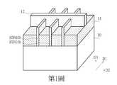
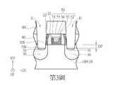
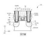
第1圖至第5圖繪示了本發明第一實施例之半導體結構的製作方法示意圖,其中第2圖繪示了第1圖之後的製作方法示意圖;第3圖繪示了第2圖之後的製作方法示意圖;第4圖繪示了第3圖之後的製作方法示意圖;第5圖繪示了第4圖之後的製作方法示意圖。FIGS. 1 to 5 are schematic diagrams of the manufacturing method of the semiconductor structure according to the first embodiment of the present invention, in whichFigure 2 shows a schematic diagram of the manufacturing method after Figure 1; Figure 3 shows a schematic diagram of the manufacturing method after Figure 2; Figure 4 shows a schematic diagram of the manufacturing method after Figure 3; Figure 5 shows Schematic diagram of the manufacturing method after Figure 4.
第6圖為第5圖中磊晶區的放大示意圖。Figure 6 is an enlarged schematic view of the epitaxial region in Figure 5.
第7圖繪示了本發明第二實施例之半導體結構的示意圖。FIG. 7 is a schematic diagram of a semiconductor structure according to a second embodiment of the invention.
第8圖繪示了本發明第三實施例之半導體結構的示意圖。FIG. 8 is a schematic diagram of a semiconductor structure according to a third embodiment of the invention.
請參閱第1圖至第6圖。第1圖至第5圖繪示了本發明第一實施例之半導體結構的製作方法示意圖,而第6圖為第5圖中磊晶區的放大示意圖。本實施例之半導體結構的製作方法包括下列步驟。如第1圖所示,提供一半導體基底10,本實施例之半導體基底10可包括矽基底、磊晶矽基底、矽鍺基底、碳化矽基底或絕緣層覆矽(silicon-on-insulator,SOI)基底,但並不以此為限。半導體基底10亦可視需要具有複數個鰭狀結構10F沿一第一方向D1延伸,且鰭狀結構10F之間可經由淺溝隔離11隔開,但並不以此為限。此外,虛置閘極(dummy gate)12可形成於鰭狀結構10F上並沿一第二方向D2延伸,而第一方向D1大體上與第二方向D2正交,但並不以此為限。接著,如第1圖至第2圖所示,於半導體基底10中形成至少一磊晶區30。在本實施例中,可於虛置閘極12於第一方向D1上的兩側分別形成磊晶區30,而磊晶區30可包括磷化矽(SiP)磊晶區、鍺化矽(SiGe)磊晶區、碳化矽(SiC)磊晶區或其他適合材料之磊晶區。此外,亦可選擇性地形成如第2圖中所示之側壁子21、接觸蝕刻停止層(contact etching stop layer,CESL)22以及第一介電層40,並可利用例如一取代金屬閘極製程(replacement metal gate process)將虛置閘極12移除而形成具有介面層51、高介電常數介電層52、閘極阻障層53、金屬閘極54以及保護層55之閘極結構50,但並不以此為限。換句話說,第一介電層40係形成於磊晶區30上,且側壁子21、接觸蝕刻停止層22、第一介電層40以及閘極結構50可藉由一平坦化製程而於一垂直半導體基底10之第三方向D3上具有相同的高度,然後再形成一第二介電層60覆蓋閘極結構50與第一介電層40。本實施例之第二介電層60可被視為一前金屬介電質沉積(pre-metal dielectric,PMD),但並不以此為限。Please refer to Figure 1 to Figure 6. FIGS. 1 to 5 are schematic diagrams of the method for manufacturing the semiconductor structure according to the first embodiment of the present invention, and FIG. 6 is an enlarged schematic diagram of the epitaxial region in FIG. 5. The manufacturing method of the semiconductor structure of this embodiment includes the following steps. As shown in FIG. 1, a
接著,如第3圖所示,可利用一圖案化光阻(未圖示)對第二介電層60與第一介電層40進行圖案化而於第一介電層40中形成一接觸孔洞H。接觸孔洞H係對應磊晶區30形成,接觸孔洞H係暴露出部分之對應的磊晶區30,且被接觸孔洞H暴露之磊晶區30上形成有一含氧化物層(oxide-containing layer)70。在本實施例中,接觸孔洞H較佳係貫穿第二介電層60、第一介電層40以及接觸蝕刻停止層22,且部分之磊晶區30係被形成接觸孔洞H之製程(例如蝕刻製程)移除。也就是說,接觸孔洞H較佳係部分延伸至磊晶區30中,藉此確保磊晶區30可被接觸孔洞H部分暴露出,但本發明並不以此為限。在本發明之其他實施例中,亦可視需要使接觸孔洞H停在磊晶區30的上表面上而未延伸至磊晶區30中。此外,值得說明的是,本實施例之含氧化物層70可由形成接觸孔洞H之製程(例如上述之蝕刻製程)所形成,而此狀況下的磊晶區30較佳為磷化矽磊晶區,且此磷化矽磊晶區係具有較高的磷濃度,例如磷濃度係高於或等於2E21個原子/平方公分(atoms/cm3),且較佳可介於2E21 atoms/cm3至5E21 atoms/cm3之間,但並不以此為限。在具有較高磷濃度之磊晶區30的狀況下,可利用磷吸引氧原子,並於形成接觸孔洞H之蝕刻製程時產生反應而形成含氧化物層70。換句話說,本實施例的製作方法可利用於形成磊晶區30時提高其磷濃度而於形成接觸孔洞H時一併形成含氧化物層70,故可不須增加其他額外的製程步驟即可形成所需之含氧化物層70。在本發明之其他實施例中,亦可視需要於接觸孔洞H形成之後,以其他方式例如含氧氣體處理、植入製程、原子層沉積(atomic layer deposition)製程或其他適合的方式於被接觸孔洞H暴露之磊晶區30上形成含氧化物層70。因此,本實施例之含氧化物層70可包括氧化矽、氧化磷以及其他適合之氧化物。Next, as shown in FIG. 3, a patterned photoresist (not shown) may be used to pattern the
在本實施例中,含氧化物層70之最上表面(例如第3圖所示之第二最上表面70S)較佳係低於磊晶區30之最上表面(例如第3圖所示之第一最上表面30S),第一最上表面30S與第二最上表面70S之間於第三方向D3上的距離(例如第3圖所示之深度DP)可控制在100埃(Angstrom)至50埃之間,且較佳為80埃,而此狀況下的含氧化物層70的厚度較佳可約為40埃,但並不以此為限。此外,當本實施例之含氧化物層70係由於形成接觸孔洞H之蝕刻製程所形成時,若此蝕刻製程為非等向性(anisotropic)的蝕刻製程,則較容易形成於中央之厚度大於在第一方向D1上兩側之厚度的含氧化物層70,而此含氧化物層70可被視為一口袋形(pocket-shaped)或半月形之含氧化物層,但本發明並不以此為限。在本發明之其他實施例中亦可視蝕刻製程的製程條件變化或其他額外用以形成含氧化物層70之製程方式狀況,而形成具有其他形狀之含氧化物層70,例如條狀含氧化物層或U字形含氧化物層,但並不以此為限。In this embodiment, the uppermost surface of the oxide-containing layer 70 (eg, the second
然後,如第4圖至第5圖所示,於含氧化物層70上以及接觸孔洞H中形成一接觸結構80。接觸結構80可包括一金屬阻障層81以及一主金屬層82。金屬阻障層81可先共形地(conformally)形成於接觸孔洞H中,而主金屬層82可在金屬阻障層81之後形成並填滿接觸孔洞H,並可再藉由一平坦化製程使得第二介電層60、金屬阻障層81以及主金屬層82的上部齊平,但並不以此為限。本實施例之金屬阻障層81可包括鎳(nickel,Ni)、鈦(titanium,Ti)、氮化鈦(titanium nitride,TiN)、鉭(tantalum,Ta)、氮化鉭(Tantalum nitride,TaN)、氧化鋁鈦(titanium aluminum oxide,TiAlO)或其他適合之導電材料的單層或多層疊層結構,而主金屬層82可包括電阻率相對較低的導電材料例如鋁(aluminum,Al)、鎢(tungsten,W)、銅(copper,Cu)等,但並不以此為限。在接觸結構80形成之後,含氧化物層70係位於接觸結構80與磊晶區30之間,藉此形成一金屬-絕緣層-矽(metal-insulator-Si)之堆疊結構,相對於未形成有含氧化物層70之金屬-矽堆疊結構可達到降低蕭基能位障高(Schottky barrier height)的效果,並進而降低接觸結構80與磊晶區30之間接觸阻抗並提升如第5圖中所形成之半導體結構101之元件性能。值得說明的是,於形成接觸孔洞H之後以及在形成金屬阻障層81之前,可視需要進行一清洗製程以移除於形成接觸孔洞H之蝕刻製程中所殘留的雜質,而由於本實施例之含氧化物層70具有一定的厚度(例如可約為40埃)且並非一般因放置於環境中所產生之自然氧化物(native oxide),故含氧化物層70並不會被清洗製程移除而可保留至進行後續製程。此外,當含氧化物層70係由形成接觸孔洞H之製程所形成時,磊晶區30的磷濃度較佳係高於或等於2E21 atoms/cm3,以形成所需的含氧化物層70。舉例來說,當磊晶區30為磷化矽磊晶區且其磷濃度僅約為1.5E21 atoms/cm3時,在形成接觸孔洞H之製程中只會形成極薄的含氧化物層並在後續清洗製中被移除。此外,依據實驗結果,在本實施例之於金屬阻障層81與磊晶區30之間形成含氧化物層70的狀況下,金屬阻障層81與磊晶區30之間的接觸阻抗可相較於未形成有含氧化物層70之狀況(例如上述之磊晶區30的磷濃度約為1.5E21 atoms/cm3時的狀況)下的接觸阻抗降低約35.6%。因此,含氧化物層70確實有助於有效降低接觸結構80與磊晶區30之間的接觸阻抗。Then, as shown in FIGS. 4 to 5, a
如第4圖至第5圖所示,本實施例之製作方法可更包括於接觸結構80與含氧化物層70之間形成一矽化物層89。矽化物層89係形成於金屬阻障層81與磊晶區30的介面處以及形成於金屬阻障層81與含氧化物層70的介面處,故矽化物層89係為一U字形矽化物層與磊晶區30以及含氧化物層70直接接觸,但並不以此為限。在本實施例中,矽化物層89包括金屬阻障層81之金屬矽化物層。舉例來說,當金屬阻障層81包括鈦時,矽化物層89則可包括矽化鈦(TiSix),但並不以此為限。此外,在本發明之其他實施例中,矽化物層89除了上述之形成方式外,亦可以其他方式例如以自對準金屬矽化物(Self-aligned silicide)方式於金屬阻障層81形成之前先形成矽化物層89,但並不以此為限。值得說明的是,在本實施例中,於形成接觸結構80之後,含氧化物層70可包括一含金屬氧化物層(metal oxide-containing layer)71。也就是說,當金屬阻障層81形成之後,除了會於介面處形成矽化物層89之外,金屬阻障層81中的成分亦可部分擴散至含氧化物層70中而使得含氧化物層70成為含金屬氧化物層71。含金屬氧化物層71可包括金屬氧化物(例如TiOx)、金屬氮氧化物(例如TiON)、含金屬與矽的氧化物(MSixOy例如TiSiO、NiSiO等)或/及含金屬與矽的氮氧化物(MSixOyNz例如TiSiON、NiSiON等),但並不以此為限。As shown in FIGS. 4 to 5, the manufacturing method of this embodiment may further include forming a
更進一步說明,如第5圖與第6圖所示,本實施例之含金屬氧化物層71可包括一第一區71A以及一第二區71B,第一區71A係位於接觸結構80與第二區71B之間,也可說是第一區71A比第二區71B靠近接觸結構80。由於擴散程度的差別,第一區71A之金屬濃度(例如鈦的含量)係高於第二區71B之金屬濃度。此外,本實施例之矽化物層89亦可為含氧的金屬矽化物層,而矽化物層89的金屬濃度係高於含金屬氧化物層71之第一區71A的金屬濃度。換句話說,由矽化物層89至含金屬氧化物層71之間的金屬濃度可呈現一逐漸降低之梯度變化,但並不以此為限。To further explain, as shown in FIGS. 5 and 6, the metal-containing
藉由上述的製作方法步驟,可形成如第5圖所示之半導體結構101。本實施例之半導體結構101可包括半導體基底10、至少一磊晶區30、接觸結構80、含氧化物層70以及矽化物層89。磊晶區30設置於半導體基底10中,接觸結構80設置於磊晶區30上,含氧化物層70設置於磊晶區30與接觸結構80之間,而矽化物層89設置於含氧化物層70與接觸結構80之間。關於半導體結構101中各部件的技術特徵已於上述製作方法中說明,故在此並不再贅述。由於接觸孔洞H係部分延伸至磊晶區30中,故於接觸孔洞H中所形成的接觸結構80之部分係於一水平方向(例如第一方向D1)上被磊晶區30圍繞,藉此亦可在有限之接觸結構80大小的狀況下增加接觸結構80與磊晶區30的接觸面積,進而達到降低阻抗的效果。此外,半導體結構101可包括閘極結構50設置在半導體基底10上,而磊晶區30可經由例如一植入製程而包括或成為一與閘極結構50對應設置之源極/汲極區。Through the above manufacturing method steps, the
此外,如第5圖與第6圖所示,本實施例之半導體結構101亦可被視為包括半導體基底10、至少一磊晶區30、接觸結構80以及含金屬氧化物層71之半導體結構。含金屬氧化物層71係設置於磊晶區30與接觸結構80之間,含金屬氧化物層71包括第一區71A以及第二區71B,第一區71A係位於接觸結構80第二區71B之間,且第一區71A之金屬濃度係高於第二區71B之金屬濃度。此外,本實施例之矽化物層89亦可為含氧的金屬矽化物層,因此矽化物層89與含氧化物層70亦可被視為一個含金屬氧化物層,其中矽化物層89可被視為此含金屬氧化物層中的第一區而具有相對較高的金屬濃度,而含氧化物層70可被視為此含金屬氧化物層中的第二區而具有相對較低的金屬濃度。In addition, as shown in FIGS. 5 and 6, the
下文將針對本發明的不同實施例進行說明,且為簡化說明,以下說明主要針對各實施例不同之處進行詳述,而不再對相同之處作重覆贅述。此外,本發明之各實施例中相同之元件係以相同之標號進行標示,以利於各實施例間互相對照。In the following, different embodiments of the present invention will be described, and to simplify the description, the following description will mainly describe the differences between the embodiments, without repeating the similarities. In addition,The same elements in the embodiments of the present invention are marked with the same reference numerals to facilitate comparison between the embodiments.
請參閱第7圖。第7圖繪示了本發明第二實施例之半導體結構102的示意圖。如第7圖所示,與上述第一實施例不同的地方在於,在本實施例之半導體結構102中,含氧化物層70為一條狀含氧化物層,含氧化物層70於中央之厚度大體上等於在第一方向D1上兩側之厚度。除了含氧化物層70的形狀之外,本實施例之半導體結構102中的其他技術特徵與上述第一實施例相似,故在此並不再贅述。Please refer to Figure 7. FIG. 7 is a schematic diagram of a
請參閱第8圖。第8圖繪示了本發明第三實施例之半導體結構103的示意圖。如第8圖所示,與上述第一實施例不同的地方在於,在本實施例之半導體結構103中,含氧化物層70為一U字形含氧化物層,故含氧化物層70與矽化物層89可具有相似的形狀。如同上述第一實施例所述的狀況,矽化物層89亦可為含氧的金屬矽化物層,因此矽化物層89與含氧化物層70亦可被視為一個含金屬氧化物層,其中矽化物層89可被視為此含金屬氧化物層中的第一區而具有相對較高的金屬濃度,而含氧化物層70可被視為此含金屬氧化物層中的第二區而具有相對較低的金屬濃度。因此,本實施例之矽化物層89與含氧化物層70之間除了於垂直之第三方向D3上具有金屬濃度逐漸改變之狀況,更於水平方向(例如第8圖中的第一方向D1)上呈現金屬濃度逐漸改變之狀況。Please refer to figure 8. FIG. 8 is a schematic diagram of a
綜上所述,本發明之半導體結構以及其製作方法係於磊晶區以及接觸結構之間形成含氧化物層或/及含金屬氧化物層,藉此降低接觸結構與磊晶區之間的蕭基能位障高(Schottky barrier height),進而達到降低接觸阻抗以及提升半導體結構元件性能之目的。此外,本發明亦可藉由控制調整磊晶區中的磷濃度,使得於形成接觸孔洞之製程中直接形成含氧化物層,故可不須其他額外的製程步驟即可形成所需之含氧化物層。以上所述僅為本發明之較佳實施例,凡依本發明申請專利範圍所做之均等變化與修飾,皆應屬本發明之涵蓋範圍。In summary, the semiconductor structure and the manufacturing method of the present invention form an oxide-containing layer or/and metal oxide-containing layer between the epitaxial region and the contact structure, thereby reducing the contact structure between the contact structure and the epitaxial region Schottky barrier height (Schottky barrier height), which in turn reduces contact impedance and improves halfThe purpose of the performance of conductor structural elements. In addition, the present invention can also control and adjust the phosphorus concentration in the epitaxial region, so that the oxide-containing layer is directly formed in the process of forming the contact hole, so the required oxide-containing layer can be formed without other additional process steps Floor. The above are only the preferred embodiments of the present invention, and all changes and modifications made in accordance with the scope of the patent application of the present invention shall fall within the scope of the present invention.
10‧‧‧半導體基底10‧‧‧Semiconductor substrate
10F‧‧‧鰭狀結構10F‧‧‧fin structure
21‧‧‧側壁子21‧‧‧Side wall
22‧‧‧接觸蝕刻停止層22‧‧‧Contact etching stop layer
30‧‧‧磊晶區30‧‧‧Epitaxial area
30S‧‧‧第一最上表面30S‧‧‧First top surface
40‧‧‧第一介電層40‧‧‧First dielectric layer
50‧‧‧閘極結構50‧‧‧Gate structure
51‧‧‧介面層51‧‧‧Interface
52‧‧‧高介電常數介電層52‧‧‧High dielectric constant dielectric layer
53‧‧‧閘極阻障層53‧‧‧ Gate barrier
54‧‧‧金屬閘極54‧‧‧Metal gate
55‧‧‧保護層55‧‧‧Protection layer
60‧‧‧第二介電層60‧‧‧Second dielectric layer
70‧‧‧含氧化物層70‧‧‧Oxide-containing layer
70S‧‧‧第二最上表面70S‧‧‧Second uppermost surface
71‧‧‧含金屬氧化物層71‧‧‧ metal oxide-containing layer
80‧‧‧接觸結構80‧‧‧Contact structure
81‧‧‧金屬阻障層81‧‧‧Metal barrier layer
82‧‧‧主金屬層82‧‧‧Main metal layer
89‧‧‧矽化物層89‧‧‧ Silicide layer
101‧‧‧半導體結構101‧‧‧Semiconductor structure
D1‧‧‧第一方向D1‧‧‧First direction
D2‧‧‧第二方向D2‧‧‧Second direction
D3‧‧‧第三方向D3‧‧‧third direction
H‧‧‧接觸孔洞H‧‧‧Contact hole
Claims (18)
Translated fromChinesePriority Applications (2)
| Application Number | Priority Date | Filing Date | Title |
|---|---|---|---|
| TW104132809ATWI682547B (en) | 2015-10-06 | 2015-10-06 | Semiconductor structure and manufacturing method thereof |
| US14/932,993US9985020B2 (en) | 2015-10-06 | 2015-11-05 | Semiconductor structure and manufacturing method thereof |
Applications Claiming Priority (1)
| Application Number | Priority Date | Filing Date | Title |
|---|---|---|---|
| TW104132809ATWI682547B (en) | 2015-10-06 | 2015-10-06 | Semiconductor structure and manufacturing method thereof |
Publications (2)
| Publication Number | Publication Date |
|---|---|
| TW201714300A TW201714300A (en) | 2017-04-16 |
| TWI682547Btrue TWI682547B (en) | 2020-01-11 |
Family
ID=58447641
Family Applications (1)
| Application Number | Title | Priority Date | Filing Date |
|---|---|---|---|
| TW104132809ATWI682547B (en) | 2015-10-06 | 2015-10-06 | Semiconductor structure and manufacturing method thereof |
Country Status (2)
| Country | Link |
|---|---|
| US (1) | US9985020B2 (en) |
| TW (1) | TWI682547B (en) |
Families Citing this family (3)
| Publication number | Priority date | Publication date | Assignee | Title |
|---|---|---|---|---|
| US10510851B2 (en)* | 2016-11-29 | 2019-12-17 | Taiwan Semiconductor Manufacturing Company, Ltd. | Low resistance contact method and structure |
| US10032672B1 (en) | 2017-08-02 | 2018-07-24 | United Microelectronics Corp. | Method of fabricating a semiconductor device having contact structures |
| US10510886B2 (en)* | 2017-10-26 | 2019-12-17 | Samsung Electronics Co., Ltd. | Method of providing reacted metal source-drain stressors for tensile channel stress |
Citations (4)
| Publication number | Priority date | Publication date | Assignee | Title |
|---|---|---|---|---|
| US20100123198A1 (en)* | 2008-11-20 | 2010-05-20 | Samsung Electronics Co., Ltd. | Semiconductor devices and methods of manufacturing the same |
| US20130032883A1 (en)* | 2011-08-04 | 2013-02-07 | International Business Machines Corporation | Fabrication of field-effect transistors with atomic layer doping |
| US20140264494A1 (en)* | 2013-03-14 | 2014-09-18 | Taiwan Semiconductor Manufacturing Company, Ltd. | Metal-Oxide-Semiconductor Field-Effect Transistor with Metal-Insulator Semiconductor Contact Structure to Reduce Schottky Barrier |
| US20150235956A1 (en)* | 2014-02-14 | 2015-08-20 | Taiwan Semiconductor Manufacturing Company Limited | Semiconductor device and formation thereof |
Family Cites Families (8)
| Publication number | Priority date | Publication date | Assignee | Title |
|---|---|---|---|---|
| KR100420121B1 (en)* | 2001-06-21 | 2004-03-02 | 삼성전자주식회사 | Ferroelectric device using ferroelectric layer as planarization layer and method of forming the same |
| US7160800B2 (en) | 2005-01-07 | 2007-01-09 | Taiwan Semiconductor Manufacturing Company, Ltd. | Decreasing metal-silicide oxidation during wafer queue time |
| JP5086665B2 (en) | 2007-03-02 | 2012-11-28 | 株式会社東芝 | Semiconductor device and manufacturing method thereof |
| US20100001317A1 (en)* | 2008-07-03 | 2010-01-07 | Yi-Wei Chen | Cmos transistor and the method for manufacturing the same |
| JP2010186877A (en) | 2009-02-12 | 2010-08-26 | Renesas Electronics Corp | Semiconductor device, and method of manufacturing the same |
| KR101952119B1 (en) | 2012-05-24 | 2019-02-28 | 삼성전자 주식회사 | Semiconductor device using metal silicide and fabricating method thereof |
| US8823065B2 (en) | 2012-11-08 | 2014-09-02 | Taiwan Semiconductor Manufacturing Company, Ltd. | Contact structure of semiconductor device |
| US9722083B2 (en) | 2013-10-17 | 2017-08-01 | Taiwan Semiconductor Manufacturing Company, Ltd. | Source/drain junction formation |
- 2015
- 2015-10-06TWTW104132809Apatent/TWI682547B/enactive
- 2015-11-05USUS14/932,993patent/US9985020B2/enactiveActive
Patent Citations (4)
| Publication number | Priority date | Publication date | Assignee | Title |
|---|---|---|---|---|
| US20100123198A1 (en)* | 2008-11-20 | 2010-05-20 | Samsung Electronics Co., Ltd. | Semiconductor devices and methods of manufacturing the same |
| US20130032883A1 (en)* | 2011-08-04 | 2013-02-07 | International Business Machines Corporation | Fabrication of field-effect transistors with atomic layer doping |
| US20140264494A1 (en)* | 2013-03-14 | 2014-09-18 | Taiwan Semiconductor Manufacturing Company, Ltd. | Metal-Oxide-Semiconductor Field-Effect Transistor with Metal-Insulator Semiconductor Contact Structure to Reduce Schottky Barrier |
| US20150235956A1 (en)* | 2014-02-14 | 2015-08-20 | Taiwan Semiconductor Manufacturing Company Limited | Semiconductor device and formation thereof |
Also Published As
| Publication number | Publication date |
|---|---|
| TW201714300A (en) | 2017-04-16 |
| US20170098707A1 (en) | 2017-04-06 |
| US9985020B2 (en) | 2018-05-29 |
Similar Documents
| Publication | Publication Date | Title |
|---|---|---|
| TWI591827B (en) | Semiconductor component and method of forming same | |
| CN107689376B (en) | Semiconductor device and method | |
| US10916468B2 (en) | Semiconductor device with buried local interconnects | |
| TWI727068B (en) | Semiconductor device and manufacturing method thereof | |
| CN102468226B (en) | Semiconductor structure and manufacturing method thereof | |
| TW202008596A (en) | Nanosheet field effect transistor with spacers between sheets | |
| TWI684258B (en) | Self-aligned metal wire on contact structure and method for forming same | |
| TW202011608A (en) | Different upper and lower spacers for contact | |
| CN107564953A (en) | Capacitance-variable transistor and its manufacture method | |
| US10685915B2 (en) | Via contact resistance control | |
| TWI682547B (en) | Semiconductor structure and manufacturing method thereof | |
| CN106558622B (en) | STI diode for ESD protection | |
| CN109638010B (en) | Radio frequency switching device and manufacturing method thereof | |
| US9142454B1 (en) | Semiconductor structure and method for manufacturing the same | |
| JP2008085205A (en) | Semiconductor device and manufacturing method thereof | |
| US8603915B2 (en) | Multi-stage silicidation process | |
| US10304839B2 (en) | Metal strap for DRAM/FinFET combination | |
| TW201539663A (en) | Semiconductor device and method of forming same | |
| TWI688042B (en) | Method of fabricating semiconductor device | |
| CN107104051B (en) | Semiconductor device and method of making the same | |
| TW201906074A (en) | Passive device structure and method of manufacturing same | |
| JPWO2014073104A1 (en) | Semiconductor device manufacturing method and semiconductor device | |
| JP2013045953A (en) | Semiconductor device and method of manufacturing the same | |
| US10269812B1 (en) | Forming contacts for VFETs | |
| JP5833214B2 (en) | Semiconductor device manufacturing method and semiconductor device |