TWI682436B - Massive transferring method of micro leds and light-emitting panel module using the method - Google Patents
Massive transferring method of micro leds and light-emitting panel module using the methodDownload PDFInfo
- Publication number
- TWI682436B TWI682436BTW107146260ATW107146260ATWI682436BTW I682436 BTWI682436 BTW I682436BTW 107146260 ATW107146260 ATW 107146260ATW 107146260 ATW107146260 ATW 107146260ATW I682436 BTWI682436 BTW I682436B
- Authority
- TW
- Taiwan
- Prior art keywords
- electrode
- doped layer
- light
- layer
- emitting diodes
- Prior art date
Links
Images


Classifications
- H—ELECTRICITY
- H01—ELECTRIC ELEMENTS
- H01L—SEMICONDUCTOR DEVICES NOT COVERED BY CLASS H10
- H01L25/00—Assemblies consisting of a plurality of semiconductor or other solid state devices
- H01L25/03—Assemblies consisting of a plurality of semiconductor or other solid state devices all the devices being of a type provided for in a single subclass of subclasses H10B, H10D, H10F, H10H, H10K or H10N, e.g. assemblies of rectifier diodes
- H01L25/04—Assemblies consisting of a plurality of semiconductor or other solid state devices all the devices being of a type provided for in a single subclass of subclasses H10B, H10D, H10F, H10H, H10K or H10N, e.g. assemblies of rectifier diodes the devices not having separate containers
- H01L25/075—Assemblies consisting of a plurality of semiconductor or other solid state devices all the devices being of a type provided for in a single subclass of subclasses H10B, H10D, H10F, H10H, H10K or H10N, e.g. assemblies of rectifier diodes the devices not having separate containers the devices being of a type provided for in group H10H20/00
- H01L25/0753—Assemblies consisting of a plurality of semiconductor or other solid state devices all the devices being of a type provided for in a single subclass of subclasses H10B, H10D, H10F, H10H, H10K or H10N, e.g. assemblies of rectifier diodes the devices not having separate containers the devices being of a type provided for in group H10H20/00 the devices being arranged next to each other
- H—ELECTRICITY
- H10—SEMICONDUCTOR DEVICES; ELECTRIC SOLID-STATE DEVICES NOT OTHERWISE PROVIDED FOR
- H10H—INORGANIC LIGHT-EMITTING SEMICONDUCTOR DEVICES HAVING POTENTIAL BARRIERS
- H10H20/00—Individual inorganic light-emitting semiconductor devices having potential barriers, e.g. light-emitting diodes [LED]
- H10H20/01—Manufacture or treatment
- H10H20/011—Manufacture or treatment of bodies, e.g. forming semiconductor layers
- H10H20/018—Bonding of wafers
- H—ELECTRICITY
- H10—SEMICONDUCTOR DEVICES; ELECTRIC SOLID-STATE DEVICES NOT OTHERWISE PROVIDED FOR
- H10H—INORGANIC LIGHT-EMITTING SEMICONDUCTOR DEVICES HAVING POTENTIAL BARRIERS
- H10H20/00—Individual inorganic light-emitting semiconductor devices having potential barriers, e.g. light-emitting diodes [LED]
- H10H20/80—Constructional details
- H10H20/84—Coatings, e.g. passivation layers or antireflective coatings
- H—ELECTRICITY
- H10—SEMICONDUCTOR DEVICES; ELECTRIC SOLID-STATE DEVICES NOT OTHERWISE PROVIDED FOR
- H10H—INORGANIC LIGHT-EMITTING SEMICONDUCTOR DEVICES HAVING POTENTIAL BARRIERS
- H10H20/00—Individual inorganic light-emitting semiconductor devices having potential barriers, e.g. light-emitting diodes [LED]
- H10H20/80—Constructional details
- H10H20/85—Packages
- H10H20/851—Wavelength conversion means
- H10H20/8511—Wavelength conversion means characterised by their material, e.g. binder
- H10H20/8512—Wavelength conversion materials
- H10H20/8513—Wavelength conversion materials having two or more wavelength conversion materials
- H—ELECTRICITY
- H10—SEMICONDUCTOR DEVICES; ELECTRIC SOLID-STATE DEVICES NOT OTHERWISE PROVIDED FOR
- H10H—INORGANIC LIGHT-EMITTING SEMICONDUCTOR DEVICES HAVING POTENTIAL BARRIERS
- H10H20/00—Individual inorganic light-emitting semiconductor devices having potential barriers, e.g. light-emitting diodes [LED]
- H10H20/80—Constructional details
- H10H20/85—Packages
- H10H20/857—Interconnections, e.g. lead-frames, bond wires or solder balls
- H—ELECTRICITY
- H10—SEMICONDUCTOR DEVICES; ELECTRIC SOLID-STATE DEVICES NOT OTHERWISE PROVIDED FOR
- H10H—INORGANIC LIGHT-EMITTING SEMICONDUCTOR DEVICES HAVING POTENTIAL BARRIERS
- H10H20/00—Individual inorganic light-emitting semiconductor devices having potential barriers, e.g. light-emitting diodes [LED]
- H10H20/01—Manufacture or treatment
- H10H20/036—Manufacture or treatment of packages
- H10H20/0361—Manufacture or treatment of packages of wavelength conversion means
- H—ELECTRICITY
- H10—SEMICONDUCTOR DEVICES; ELECTRIC SOLID-STATE DEVICES NOT OTHERWISE PROVIDED FOR
- H10H—INORGANIC LIGHT-EMITTING SEMICONDUCTOR DEVICES HAVING POTENTIAL BARRIERS
- H10H20/00—Individual inorganic light-emitting semiconductor devices having potential barriers, e.g. light-emitting diodes [LED]
- H10H20/01—Manufacture or treatment
- H10H20/036—Manufacture or treatment of packages
- H10H20/0364—Manufacture or treatment of packages of interconnections
- H—ELECTRICITY
- H10—SEMICONDUCTOR DEVICES; ELECTRIC SOLID-STATE DEVICES NOT OTHERWISE PROVIDED FOR
- H10H—INORGANIC LIGHT-EMITTING SEMICONDUCTOR DEVICES HAVING POTENTIAL BARRIERS
- H10H20/00—Individual inorganic light-emitting semiconductor devices having potential barriers, e.g. light-emitting diodes [LED]
- H10H20/80—Constructional details
- H10H20/85—Packages
- H10H20/851—Wavelength conversion means
- H10H20/8514—Wavelength conversion means characterised by their shape, e.g. plate or foil
Landscapes
- Engineering & Computer Science (AREA)
- Power Engineering (AREA)
- Microelectronics & Electronic Packaging (AREA)
- Physics & Mathematics (AREA)
- Condensed Matter Physics & Semiconductors (AREA)
- General Physics & Mathematics (AREA)
- Computer Hardware Design (AREA)
- Led Device Packages (AREA)
Abstract
Description
Translated fromChinese本申請案涉及顯示領域,特別是一種微型發光二極體巨量轉移的方法及該方法所製作的發光面板組件。The present application relates to the field of display, in particular to a method for mass transfer of miniature light-emitting diodes and a light-emitting panel assembly manufactured by the method.
數位顯示螢幕已滲透到生活中的各種領域,現行以液晶顯示器(Liquid Crystal Display,LCD)最為普及,但使用者的需求上,更期望能夠達到更高亮度、更高彩度的效能。以現行來看,雖然有機發光二極體(Organic Light-Emitting Diode,OLED)能夠具有高亮度、高彩度等優點,但是OLED有其壽命上的限制。例如,現有應用OLED的顯示器、手機或手錶,都因為OLED本身有機材料的特性,在使用一段時間(例如2000小時後),會產生「烙印」的現象,而縮減了產品的使用年限。Digital display screens have penetrated into various fields of life. Currently, liquid crystal displays (LCD) are the most popular. However, users demand that they can achieve higher brightness and higher chroma performance. At present, although organic light-emitting diodes (Organic Light-Emitting Diode, OLED) can have the advantages of high brightness, high chroma, etc., but OLED has its limitations in life. For example, existing displays, mobile phones, or watches that use OLEDs, because of the characteristics of OLED's own organic materials, will produce a "burn-in" phenomenon after a period of use (for example, after 2000 hours), which reduces the product's service life.
LED同樣可達到高亮度、高彩度的效果,但是首先要滿足發光源的尺寸、以及色塊排列的問題,現行技術上,是將R、G、B的發光二極體都分開製作,再透過轉移,例如,以沾黏等方式裝設到電路板上。但是為了提升解析度,必須伴隨著隨著LED尺寸縮小。在現行的LED轉移的方式,最大的缺點在於排列的精度無法提升。另外,隨著LED尺寸縮小,將LED晶粒從晶圓切割時,亦可能可能會因為切割或是轉移上的問題,而造成LED晶粒的損傷、或是電性特性不佳等問題,而影響了後續產品的良率。LED can also achieve the effect of high brightness and high chroma, but first of all to meet the problem of the size of the light source and the arrangement of color blocks. In the current technology, the light-emitting diodes of R, G, and B are made separately, and then transferred through For example, it is mounted on the circuit board by means of adhesion. But in order to improve the resolution, it must be accompanied by the shrinking of LED size. In the current LED transfer method, the biggest disadvantage is that the accuracy of the arrangement cannot be improved. In addition, as the LED size shrinks, the LED die may be cut from the wafer due to cutting or transfer problems.Problems such as damage to the LED die or poor electrical characteristics have affected the yield of subsequent products.
在此,提供一種微型發光二極體巨量轉移的方法。微型發光二極體巨量轉移的方法,包含微型發光二極體製作步驟、連接步驟、移除步驟、螢光粉層形成步驟、以及濾光片形成步驟。微型發光二極體製作步驟是形成複數個微型發光二極體於晶圓基板上,各微型發光二極體包含第一電極及第二電極。連接步驟是將包含微型發光二極體的晶圓基板與電路載板連接。電路載板上包含複數個第一電性連接部及複數個第二電性連接部,第一電性連接部分別與微型發光二極體之第一電極連接,第二電性連接部分別與微型發光二極體之第二電極連接。移除步驟是移除晶圓基板。螢光粉層形成步驟是在微型發光二極體的表面形成螢光粉層。濾光片形成步驟是貼附複數個濾光片於螢光粉層上,各濾光片對應於各微型發光二極體的出光面。Here, a method for mass transfer of miniature light-emitting diodes is provided. A method for mass transfer of miniature light-emitting diodes includes a miniature light-emitting diode manufacturing step, a connecting step, a removing step, a phosphor layer forming step, and a filter forming step. The manufacturing step of the miniature light emitting diode is to form a plurality of miniature light emitting diodes on the wafer substrate, and each miniature light emitting diode includes a first electrode and a second electrode. The connecting step is to connect the wafer substrate containing the micro light-emitting diodes to the circuit carrier board. The circuit board includes a plurality of first electrical connection parts and a plurality of second electrical connection parts, the first electrical connection parts are respectively connected to the first electrodes of the miniature light emitting diodes, and the second electrical connection parts are respectively connected to The second electrode of the miniature light emitting diode is connected. The removal step is to remove the wafer substrate. The phosphor layer forming step is to form a phosphor layer on the surface of the miniature light emitting diode. The forming step of the filter is to attach a plurality of filters to the phosphor layer, and each filter corresponds to the light emitting surface of each micro light-emitting diode.
在一些實施例中,微型發光二極體製作步驟包含摻雜半導體層形成步驟、圖案化步驟、絕緣層形成步驟、及電極形成步驟。摻雜半導體層形成步驟是在晶圓基板上依序形成第一型摻雜半導體材料層及第二型摻雜半導體材料層。圖案化步驟是將第一型摻雜半導體材料層及第二型摻雜半導體材料層圖案化形成複數個半導體圖案,各半導體圖案中具有第一摻雜層及第二摻雜層,第二摻雜層的長度小於第一摻雜層的長度。絕緣層形成步驟是形成絕緣層於第一摻雜層及第二摻雜層之上。絕緣層包含第一穿孔及第二穿孔,第一穿孔及第二穿孔分別曝露出第一摻雜層及第二摻雜層的一部分。電極形成步驟是形成第一電極及第二電極於絕緣層上。第一電極的一部分填入第一穿孔中並與第一摻雜層連接,第二電極的一部分填入第二穿孔中並與第二摻雜層連接,第一電極及第二電極藉由絕緣層彼此分隔。In some embodiments, the miniature light emitting diode manufacturing step includes a doped semiconductor layer forming step, a patterning step, an insulating layer forming step, and an electrode forming step. The step of forming the doped semiconductor layer is to sequentially form a first-type doped semiconductor material layer and a second-type doped semiconductor material layer on the wafer substrate. The patterning step is to pattern the first type doped semiconductor material layer and the second type doped semiconductor material layer to form a plurality of semiconductor patterns, each semiconductor pattern has a first doped layer and a second doped layer, the second doped The length of the impurity layer is smaller than the length of the first doped layer. The insulating layer forming step is to form an insulating layer on the first doped layer and the second doped layer. The insulating layer includes a first through hole and a second through hole, the first through hole and the second through hole expose the first doped layer and the second doped layer, respectivelyPart of the miscellaneous layer. The electrode forming step is to form the first electrode and the second electrode on the insulating layer. A part of the first electrode is filled in the first through hole and connected with the first doped layer, a part of the second electrode is filled in the second through hole and connected with the second doped layer, the first electrode and the second electrode are insulated by The layers are separated from each other.
進一步地,在一些實施例中,第一電極更遮蔽第一摻雜層的第一側表面。第二電極更遮蔽第一摻雜層及第二摻雜層的第二側表面,第二側表面相對於第一側表面。Further, in some embodiments, the first electrode further shields the first side surface of the first doped layer. The second electrode further shields the second side surface of the first doped layer and the second doped layer, and the second side surface is opposite to the first side surface.
進一步地,在一些實施例中,出光面為第一摻雜層設置於晶圓基板的表面,各微型發光二極體的出光面實質上位於同一平面。Further, in some embodiments, the light exit surface is a surface on which the first doped layer is disposed on the wafer substrate, and the light exit surfaces of the micro-emitting diodes are substantially on the same plane.
在一些實施例中,電路載板為特用晶片。In some embodiments, the circuit carrier is a special wafer.
在一些實施例中,微型發光二極體巨量轉移的方法更包含晶片連接步驟,晶片連接步驟係將電路載板的接線區與特用晶片連接。In some embodiments, the method for mass transfer of miniature light emitting diodes further includes a wafer connection step. The wafer connection step connects the wiring area of the circuit carrier board with a special wafer.
在此,還提供一種發光面板組件。發光面板組件包含電路載板、複數個微型發光二極體、螢光粉層、以及複數個濾光片。電路載板包含複數個第一電性連接部及複數個第二電性連接部。各微型發光二極體包含第一摻雜層、第二摻雜層、第一電極及第二電極。第一摻雜層與第二摻雜層相互堆疊,第一摻雜層的第一表面為出光面,且第一摻雜層的長度大於第二摻雜層的長度。第一電極與第二電極彼此分隔,各第一電極與第一摻雜層的連接面以及第一電性連接部之一連接,各第二電極與第二摻雜層及第二電性連接部之一連接,連接面相對於出光面,且微型發光二極體的出光面實質上位於同一平面。螢光粉層位於微型發光二極體之出光面之上。複數個濾光片設置於螢光粉層上,各濾光片對應於各微型發光二極體的出光面。Here, a light-emitting panel assembly is also provided. The light-emitting panel assembly includes a circuit carrier board, a plurality of miniature light-emitting diodes, a phosphor layer, and a plurality of filters. The circuit board includes a plurality of first electrical connections and a plurality of second electrical connections. Each miniature light emitting diode includes a first doped layer, a second doped layer, a first electrode and a second electrode. The first doped layer and the second doped layer are stacked on each other. The first surface of the first doped layer is a light exit surface, and the length of the first doped layer is greater than the length of the second doped layer. The first electrode and the second electrode are separated from each other, each first electrode is connected to the connection surface of the first doped layer and one of the first electrical connection portions, and each second electrode is connected to the second doped layer and the second electrical connection One of the parts is connected, the connecting surface is opposite to the light-emitting surface, and the light-emitting surface of the miniature light-emitting diode is substantially on the same plane. The phosphor layer is located on the light emitting surface of the miniature light emitting diode. A plurality of filters are arranged on the phosphor layer, and each filter corresponds to each miniature light emitting diodeThe light side.
在一些實施例中,第一電極與第二電極之間以絕緣層相互隔絕。進一步地,在一些實施例中,第一電極更遮蔽第一摻雜層的第一側表面。第二電極更遮蔽第一摻雜層及第二摻雜層的第二側表面,第二側表面相對於第一側表面。In some embodiments, the first electrode and the second electrode are insulated from each other by an insulating layer. Further, in some embodiments, the first electrode further shields the first side surface of the first doped layer. The second electrode further shields the second side surface of the first doped layer and the second doped layer, and the second side surface is opposite to the first side surface.
在一些實施例中,電路載板為特用晶片。In some embodiments, the circuit carrier is a special wafer.
在一些實施例中,發光面板組件更包含特用晶片,特用晶片連接電路載板的接線區。In some embodiments, the light-emitting panel assembly further includes a special wafer, which is connected to the wiring area of the circuit carrier board.
在一些實施例中,各濾光片的長度大於對應之出光面的長度。In some embodiments, the length of each filter is greater than the length of the corresponding light exit surface.
在此,微型發光二極體巨量轉移的方法是藉由直接將晶圓基板上的微型發光二極體,直接對應地連接電路載板的電性連接部,來完成電性連接,再將晶圓基板移除。從而,轉移精度及產品良率能大幅提升、進一步還可以達到製程快速的優點。Here, the method of mass transfer of miniature light-emitting diodes is to directly connect the miniature light-emitting diodes on the wafer substrate to the electrical connection part of the circuit board directly to complete the electrical connection, and then Wafer substrate removal. Therefore, the transfer accuracy and product yield can be greatly improved, and furthermore, the advantages of rapid process can be achieved.
1‧‧‧發光面板組件1‧‧‧Lighting panel assembly
2‧‧‧半導體圖案2‧‧‧Semiconductor pattern
3‧‧‧微型發光二極體3‧‧‧Miniature LED
10‧‧‧第一摻雜層10‧‧‧First doped layer
11‧‧‧出光面11‧‧‧Glossy
131‧‧‧第一側表面131‧‧‧First side surface
133‧‧‧第二側表面133‧‧‧Second side surface
17‧‧‧連接面17‧‧‧Connecting surface
20‧‧‧第二摻雜層20‧‧‧Second doped layer
233‧‧‧第二側表面233‧‧‧Second side surface
30‧‧‧絕緣層30‧‧‧Insulation
41‧‧‧第一電極41‧‧‧First electrode
43‧‧‧第二電極43‧‧‧Second electrode
157‧‧‧組接面157‧‧‧ group joint
60‧‧‧螢光粉層60‧‧‧ phosphor powder layer
65‧‧‧螢光粉65‧‧‧fluorescent powder
70R、70B、70G‧‧‧濾光片70R, 70B, 70G ‧‧‧ filter
100‧‧‧第一型摻雜半導體材料層100‧‧‧
200‧‧‧第二型摻雜半導體材料層200‧‧‧
150‧‧‧電路載板150‧‧‧ circuit board
151‧‧‧第一電性連接部151‧‧‧The first electrical connection
153‧‧‧第二電性連接部153‧‧‧Second electrical connection
155‧‧‧接線區155‧‧‧Wiring area
170‧‧‧特用晶片170‧‧‧ Special chip
500‧‧‧晶圓基板500‧‧‧ Wafer substrate
V1‧‧‧第一穿孔V1‧‧‧ First punch
V2‧‧‧第二穿孔V2‧‧‧Second Perforation
S1‧‧‧微型發光二極體巨量轉移的方法S1‧‧‧Method for mass transfer of miniature light-emitting diodes
S10‧‧‧微型發光二極體製作步驟S10‧‧‧Miniature LED production steps
S20‧‧‧連接步驟S20‧‧‧ connection procedure
S11‧‧‧摻雜半導體層形成步驟S11‧‧‧Doped semiconductor layer forming step
S13‧‧‧圖案化步驟S13‧‧‧patterning steps
S15‧‧‧絕緣層形成步驟S15‧‧‧Insulation layer formation steps
S17‧‧‧電極形成步驟S17‧‧‧electrode forming steps
S30‧‧‧移除步驟S30‧‧‧Removal steps
S40‧‧‧螢光粉層形成步驟S40‧‧‧Phosphor powder layer forming steps
S50‧‧‧濾光片形成步驟S50‧‧‧ filter formation steps
S60‧‧‧晶片連接步驟S60‧‧‧chip connection steps
圖1為微型發光二極體巨量轉移的方法的流程圖。FIG. 1 is a flowchart of a method for mass transfer of miniature light emitting diodes.
圖2至圖10為微型發光二極體巨量轉移的方法的剖面示意圖。2 to 10 are schematic cross-sectional views of a method for mass transfer of miniature light emitting diodes.
圖11為發光面板組件另一實施例的剖面示意圖。11 is a schematic cross-sectional view of another embodiment of a light-emitting panel assembly.
圖1為微型發光二極體巨量轉移的方法的流程圖。圖2至圖10為微型發光二極體巨量轉移的方法的剖面示意圖。如圖1所示,微型發光二極體巨量轉移的方法S1包含微型發光二極體製作步驟S10、連接步驟S20、移除步驟S30、螢光粉層形成步驟S40、以及濾光片形成步驟S50。FIG. 1 is a flowchart of a method for mass transfer of miniature light emitting diodes. 2 to 10 are schematic cross-sectional views of a method for mass transfer of miniature light emitting diodes. As shown in Figure 1, the micro hairThe method S1 for mass transfer of photodiodes includes a miniature light emitting diode manufacturing step S10, a connecting step S20, a removing step S30, a phosphor layer forming step S40, and a filter forming step S50.
在一些實施例中,微型發光二極體製作步驟S10包含摻雜半導體層形成步驟S11、圖案化步驟S13、絕緣層形成步驟S15、及電極形成步驟S17。如圖2所示,摻雜半導體層形成步驟S11是在晶圓基板500上依序形成第一型摻雜半導體材料層100及第二型摻雜半導體材料層200。例如,晶圓基板500為藍寶石晶圓基板、第一型摻雜半導體材料層100為n型摻雜半導體、第二型摻雜半導體材料層200為p型半導體層。然而,以上僅為示例,而非限於此。In some embodiments, the micro light emitting diode manufacturing step S10 includes a doped semiconductor layer forming step S11, a patterning step S13, an insulating layer forming step S15, and an electrode forming step S17. As shown in FIG. 2, the doped semiconductor layer forming step S11 is to sequentially form the first-type doped
如圖3所示,圖案化步驟S13是將第一型摻雜半導體材料層100及第二型摻雜半導體材料層200圖案化形成複數個半導體圖案2,各半導體圖案2中具有第一摻雜層10及第二摻雜層20,第二摻雜層20的長度小於第一摻雜層10的長度。也就是,可以透過微影、蝕刻等方式,將第一型摻雜半導體材料層100圖案化為複數個第一摻雜層10、將第二型摻雜半導體材料層200圖案化為複數個第二摻雜層20。在此,各半導體圖案2的第一摻雜層10及第二摻雜層20的連接面17,形成一p-n接面(p-n junction)。As shown in FIG. 3, the patterning step S13 is to pattern the first-type doped
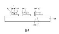
如圖4所示,絕緣層形成步驟S15是形成絕緣層30於第一摻雜層10及第二摻雜層20之上。絕緣層30包含第一穿孔V1及第二穿孔V2,第一穿孔V1及第二穿孔V2分別曝露出第一摻雜層10及第二摻雜層20的一部分。在此,可以利用滾塗的方式形成絕緣材料層,再以微影技術、或是電漿蝕刻的方式開設出第一穿孔V1及第二穿孔V2,而完成絕緣層30的製作。As shown in FIG. 4, the insulating layer forming step S15 is to form the insulating
如圖5所示,電極形成步驟S17是形成第一電極41及第二電極43於絕緣層30上。第一電極41的一部分填入第一穿孔V1中並與第一摻雜層10連接,第二電極43的一部分填入第二穿孔V2中並與第二摻雜層20連接,第一電極41及第二電極43藉由絕緣層30彼此分隔,且第一電極41與第二電極43具有不同的高度。如此,形成複數個相同的微型發光二極體(micro light-emitting diode,Micro LED)3於晶圓基板500上。然而,以上步驟僅為示例,而不限於此,微型發光二極體製作步驟S10適用於在晶圓製程中製作微型發光二極體3於晶圓基板500的方法。As shown in FIG. 5, the electrode forming step S17 is to form the
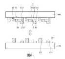
如圖6及圖7所示,連接步驟S20是將包含微型發光二極體3的晶圓基板500與電路載板150連接。電路載板150上包含複數個第一電性連接部151及複數個第二電性連接部153,第一電性連接部151及第二電性連接部153係位於電路載板150的組接面157上,且具有不同的高度,以分別對應連接第一電極41及第二電極43,組接面157面對微型發光二極體3。第一電性連接部151分別與微型發光二極體3之第一電極41連接,第二電性連接部153分別與微型發光二極體3之第二電極43連接。在此,第一電性連接部151及第二電性連接部153可以為錫球、或是導電柱(bump),第一電性連接部151及第二電性連接部153可具有不同的高度,以利於第一電極41及第二電極43連接。但這僅為示例,而非用以限制。As shown in FIGS. 6 and 7, the connection step S20 is to connect the
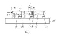
如圖8所示,移除步驟S30是移除晶圓基板500。使得第一摻雜層10與晶圓基板500交接表面,可以做為微型發光二極體3的出光面11。在此,出光面11與連接面17位於第一摻雜層10相對的兩面,此外,由於第一摻雜層10是形成在平坦的晶圓基板500上,經移除晶圓基板500後,各微型發光二極體3的出光面11實質上位於同一平面,在此,「實質上」是表示巨觀上位於同一平面,但微觀上容許有製程上的公差存在。As shown in FIG. 8, the removing step S30 is to remove the
如圖9所示,螢光粉層形成步驟S40是在微型發光二極體3的表面形成連續的螢光粉層60。在此,微型發光二極體3可以全為白光二極體,或是全為藍光二極體,透過螢光粉層60中的複數個螢光粉65,可以使得由出光面11射出的光線,進一步激發螢光粉65,而使得色域更擴大。在此,螢光粉65也可以是量子點。在此僅為示例,而非限於此。As shown in FIG. 9, the phosphor layer forming step S40 is to form a
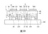
如圖10所示,濾光片形成步驟S50是貼附複數個濾光片70R、70G、70B於螢光粉層60上,各濾光片70R、70G、70B對應於各微型發光二極體3的出光面11。70R、70G、70B是表示紅、綠、藍三原光的濾光片,如此,可以形成畫素的排列。在此,濾光片70R、70G、70B的排列順序僅為示例,而非限於此,依據畫素排列的設計而定。貼附的方式可以利用現有各種方式來將濾光片70R、70G、70B貼附到特定位置。在此,若是微型發光二極體3為白光二極體,特定的位置也可以不貼附濾光片,以提高像素亮度。如此,完成發光面板組件1。此外,濾光片70R、70G、70B的長度大於對應之出光面11的長度,如此,以避免漏光。As shown in FIG. 10, the filter forming step S50 is to attach a plurality of
在此,電路載板150可以為特用晶片(Application specific integrated circuit,ASIC)。另外,如圖10所示,微型發光二極體3的第一電極41更遮蔽第一摻雜層10的第一側表面131;第二電極43更遮蔽第一摻雜層10及第二摻雜層20的第二側表面133、233,第二側表面133、233相對於第一側表面131。由於第一電極41、第二電極43為金屬材料,可以達到遮光及反射的功效,能將由第一側表面131或第二側表面133、233發出的光線反射,而朝向出光面11發出。Here, the
圖11為發光面板組件另一實施例的剖面示意圖。同時參見圖1及圖11,微型發光二極體巨量轉移的方法S1更包含晶片連接步驟S60,晶片連接步驟S60係將電路載板150的接線區155與特用晶片170連接。如此,特用晶片170的尺寸可以做得更小。在此,接線區155與特用晶片170的位置僅為示例,而非限於此。另外,晶片連接步驟S60的順序,亦可以在連接步驟S20之前,並非一定在最後才進行。11 is a schematic cross-sectional view of another embodiment of a light-emitting panel assembly. 1 and FIG. 11 at the same time, the method S1 for mass transfer of miniature light emitting diodes further includes a chip connection step S60, which connects the
綜上所述,微型發光二極體巨量轉移的方法S1是藉由直接將晶圓基板500上的微型發光二極體3直接對應地連接電路載板150的電性連接部151、153完成電性連接,再將晶圓基板500移除。如此,不需透過切割晶粒、黏膠轉移等步驟,而直接以晶圓等級的技術進行,以此達到高精度、高良率、製程快速的優點。In summary, the method S1 for the mass transfer of miniature light-emitting diodes is achieved by directly connecting the miniature light-emitting
雖然本發明的技術內容已經以較佳實施例揭露如上,然其並非用以限定本發明,任何熟習此技藝者,在不脫離本發明之精神所作些許之更動與潤飾,皆應涵蓋於本發明的範疇內,因此本發明之保護範圍當視後附之申請專利範圍所界定者為準。Although the technical content of the present invention has been disclosed as above with preferred embodiments, it is not intended to limit the present invention. Anyone who is familiar with this art and makes some changes and retouching without departing from the spirit of the present invention should be covered in the present invention. The scope of protection of the present invention shall be subject to the scope of the attached patent application.
2‧‧‧半導體圖案2‧‧‧Semiconductor pattern
10‧‧‧第一摻雜層10‧‧‧First doped layer
11‧‧‧出光面11‧‧‧Glossy
131‧‧‧第一側表面131‧‧‧First side surface
133‧‧‧第二側表面133‧‧‧Second side surface
17‧‧‧連接面17‧‧‧Connecting surface
20‧‧‧第二摻雜層20‧‧‧Second doped layer
233‧‧‧第二側表面233‧‧‧Second side surface
30‧‧‧絕緣層30‧‧‧Insulation
41‧‧‧第一電極41‧‧‧First electrode
43‧‧‧第二電極43‧‧‧Second electrode
150‧‧‧電路載板150‧‧‧ circuit board
151‧‧‧第一電性連接部151‧‧‧The first electrical connection
153‧‧‧第二電性連接部153‧‧‧Second electrical connection
500‧‧‧晶圓基板500‧‧‧ Wafer substrate
3‧‧‧微型發光二極體3‧‧‧Miniature LED
Claims (11)
Translated fromChinesePriority Applications (2)
| Application Number | Priority Date | Filing Date | Title |
|---|---|---|---|
| TW107146260ATWI682436B (en) | 2018-12-20 | 2018-12-20 | Massive transferring method of micro leds and light-emitting panel module using the method |
| US16/460,782US20200203319A1 (en) | 2018-12-20 | 2019-07-02 | Mass transfer method for micro light emitting diode and light emitting panel module using thereof |
Applications Claiming Priority (1)
| Application Number | Priority Date | Filing Date | Title |
|---|---|---|---|
| TW107146260ATWI682436B (en) | 2018-12-20 | 2018-12-20 | Massive transferring method of micro leds and light-emitting panel module using the method |
Publications (2)
| Publication Number | Publication Date |
|---|---|
| TWI682436Btrue TWI682436B (en) | 2020-01-11 |
| TW202025240A TW202025240A (en) | 2020-07-01 |
Family
ID=69942452
Family Applications (1)
| Application Number | Title | Priority Date | Filing Date |
|---|---|---|---|
| TW107146260ATWI682436B (en) | 2018-12-20 | 2018-12-20 | Massive transferring method of micro leds and light-emitting panel module using the method |
Country Status (2)
| Country | Link |
|---|---|
| US (1) | US20200203319A1 (en) |
| TW (1) | TWI682436B (en) |
Cited By (4)
| Publication number | Priority date | Publication date | Assignee | Title |
|---|---|---|---|---|
| WO2021233095A1 (en)* | 2020-05-22 | 2021-11-25 | 北京芯海视界三维科技有限公司 | Light-emitting module, display module, display screen, and display |
| TWI751672B (en)* | 2020-08-31 | 2022-01-01 | 錼創顯示科技股份有限公司 | Micro led display device and manufacturing method thereof |
| TWI754283B (en)* | 2020-05-19 | 2022-02-01 | 大陸商深超光電(深圳)有限公司 | Method for making display panel |
| CN114759130A (en)* | 2022-06-15 | 2022-07-15 | 镭昱光电科技(苏州)有限公司 | Micro-LED display chip and preparation method thereof |
Families Citing this family (18)
| Publication number | Priority date | Publication date | Assignee | Title |
|---|---|---|---|---|
| US11776460B2 (en) | 2019-03-29 | 2023-10-03 | Creeled, Inc. | Active control of light emitting diodes and light emitting diode displays |
| US11727857B2 (en) | 2019-03-29 | 2023-08-15 | Creeled, Inc. | Active control of light emitting diodes and light emitting diode displays |
| US11790831B2 (en) | 2019-03-29 | 2023-10-17 | Creeled, Inc. | Active control of light emitting diodes and light emitting diode displays |
| US11694601B2 (en) | 2019-03-29 | 2023-07-04 | Creeled, Inc. | Active control of light emitting diodes and light emitting diode displays |
| US12142716B2 (en) | 2019-03-29 | 2024-11-12 | Creeled, Inc. | Active control of light emitting diodes and light emitting diode displays |
| US12198605B2 (en) | 2019-03-29 | 2025-01-14 | Creeled, Inc. | Active control of light emitting diodes and light emitting diode displays |
| US11695102B2 (en)* | 2020-06-19 | 2023-07-04 | Creeled, Inc. | Active electrical elements with light-emitting diodes |
| CN112071795A (en)* | 2020-09-10 | 2020-12-11 | Tcl华星光电技术有限公司 | Transfer method of Micro-LED chip |
| TWI756858B (en)* | 2020-10-06 | 2022-03-01 | 吳伯仁 | System and method for making micro led display |
| CN112201651B (en)* | 2020-10-29 | 2025-04-15 | 江苏稳润光电有限公司 | A multi-color temperature COB light source |
| CN114730786A (en) | 2020-11-06 | 2022-07-08 | 京东方科技集团股份有限公司 | Light emitting diode chip, preparation method thereof and display device |
| CN112802941A (en)* | 2020-12-30 | 2021-05-14 | 深圳市华星光电半导体显示技术有限公司 | Display panel |
| CN113421954B (en)* | 2021-05-21 | 2023-06-09 | 友达光电股份有限公司 | Display device and method for manufacturing the same |
| CN113345927B (en)* | 2021-05-31 | 2023-06-02 | 武汉华星光电技术有限公司 | Preparation method of under-screen camera display panel and transparent display area |
| EP4476714A1 (en) | 2022-02-07 | 2024-12-18 | Creeled, Inc. | Light-emitting diodes with mixed clock domain signaling |
| US12014673B2 (en) | 2022-02-07 | 2024-06-18 | Creeled, Inc. | Light-emitting diodes with mixed clock domain signaling |
| US12014677B1 (en) | 2023-04-10 | 2024-06-18 | Creeled, Inc. | Light-emitting diode packages with transformation and shifting of pulse width modulation signals and related methods |
| US12437707B2 (en) | 2023-09-27 | 2025-10-07 | Creeled, Inc. | Pseudo-exponential encoding for light-emitting devices and related methods |
Citations (2)
| Publication number | Priority date | Publication date | Assignee | Title |
|---|---|---|---|---|
| US20160218095A1 (en)* | 2015-01-22 | 2016-07-28 | Kabushiki Kaisha Toshiba | Composite resin and electronic device |
| US20170345802A1 (en)* | 2016-05-31 | 2017-11-30 | Lg Electronics Inc. | Display device using semiconductor light emitting device and fabrication method thereof |
Family Cites Families (8)
| Publication number | Priority date | Publication date | Assignee | Title |
|---|---|---|---|---|
| US9111464B2 (en)* | 2013-06-18 | 2015-08-18 | LuxVue Technology Corporation | LED display with wavelength conversion layer |
| KR102135352B1 (en)* | 2013-08-20 | 2020-07-17 | 엘지전자 주식회사 | Display |
| US10229630B2 (en)* | 2014-05-14 | 2019-03-12 | The Hong Kong University Of Science And Technology | Passive-matrix light-emitting diodes on silicon micro-display |
| TWI578574B (en)* | 2014-07-14 | 2017-04-11 | 新世紀光電股份有限公司 | Light-emitting element structure |
| US10153257B2 (en)* | 2016-03-03 | 2018-12-11 | X-Celeprint Limited | Micro-printed display |
| CN116469883A (en)* | 2016-04-01 | 2023-07-21 | 首尔半导体株式会社 | Display module and display device |
| US10529696B2 (en)* | 2016-04-12 | 2020-01-07 | Cree, Inc. | High density pixelated LED and devices and methods thereof |
| CN106876406B (en)* | 2016-12-30 | 2023-08-08 | 上海君万微电子科技有限公司 | LED full-color display device structure based on III-V nitride semiconductor and preparation method thereof |
- 2018
- 2018-12-20TWTW107146260Apatent/TWI682436B/ennot_activeIP Right Cessation
- 2019
- 2019-07-02USUS16/460,782patent/US20200203319A1/ennot_activeAbandoned
Patent Citations (2)
| Publication number | Priority date | Publication date | Assignee | Title |
|---|---|---|---|---|
| US20160218095A1 (en)* | 2015-01-22 | 2016-07-28 | Kabushiki Kaisha Toshiba | Composite resin and electronic device |
| US20170345802A1 (en)* | 2016-05-31 | 2017-11-30 | Lg Electronics Inc. | Display device using semiconductor light emitting device and fabrication method thereof |
Cited By (5)
| Publication number | Priority date | Publication date | Assignee | Title |
|---|---|---|---|---|
| TWI754283B (en)* | 2020-05-19 | 2022-02-01 | 大陸商深超光電(深圳)有限公司 | Method for making display panel |
| WO2021233095A1 (en)* | 2020-05-22 | 2021-11-25 | 北京芯海视界三维科技有限公司 | Light-emitting module, display module, display screen, and display |
| TWI751672B (en)* | 2020-08-31 | 2022-01-01 | 錼創顯示科技股份有限公司 | Micro led display device and manufacturing method thereof |
| US11843024B2 (en) | 2020-08-31 | 2023-12-12 | PlayNitride Display Co., Ltd. | Micro LED display device and manufacturing method thereof |
| CN114759130A (en)* | 2022-06-15 | 2022-07-15 | 镭昱光电科技(苏州)有限公司 | Micro-LED display chip and preparation method thereof |
Also Published As
| Publication number | Publication date |
|---|---|
| TW202025240A (en) | 2020-07-01 |
| US20200203319A1 (en) | 2020-06-25 |
Similar Documents
| Publication | Publication Date | Title |
|---|---|---|
| TWI682436B (en) | Massive transferring method of micro leds and light-emitting panel module using the method | |
| TWI673863B (en) | Micro LED display and manufacturing method thereof | |
| US10304901B1 (en) | Micro light-emitting diode display device and manufacturing method thereof | |
| TWI689092B (en) | Micro led display module having light transmissive substrate and manufacturing method thereof | |
| US9825013B2 (en) | Transfer-bonding method for the light emitting device and light emitting device array | |
| CN103579461B (en) | Prepare the method for wafer scale full-color LED display array | |
| WO2019223567A1 (en) | Display substrate, display apparatus, and manufacturing method for display substrate | |
| CN112928196B (en) | Display panel, manufacturing method thereof and display device | |
| WO2012148234A2 (en) | Full-color led display apparatus and method for manufacturing same | |
| WO2015123907A1 (en) | Full-colour led display panel and manufacturing method therefor, display and electronic product | |
| CN110429097A (en) | A kind of preparation method of display panel, display device and display panel | |
| TWI627740B (en) | Micro light emitting diode display module and manufacturing method thereof | |
| TWI611573B (en) | Method for manufacturing micro light emitting diode display module | |
| WO2022082903A1 (en) | Full-color micro led array structure and preparation method therefor | |
| CN112310142B (en) | Display device, display panel and manufacturing method thereof | |
| CN109037263A (en) | Micro- light-emitting diode display module and its manufacturing method with light-transmitting substrate | |
| CN119546027A (en) | A micro display module and a method for preparing the same | |
| CN113035854A (en) | Integrated chip, manufacturing method thereof, full-color integrated chip and display panel | |
| TW202310391A (en) | Micro light emitting diode display device | |
| TWI685987B (en) | Micro-die module transfer method | |
| TWI646377B (en) | Display device and method of manufacturing same | |
| CN111354841A (en) | Method for transferring mass of micro light-emitting diode and light-emitting panel assembly thereof | |
| CN110010016A (en) | Display panel | |
| TWI467808B (en) | Light-emitting diode element, manufacturing method thereof and light-emitting device | |
| CN117038699B (en) | GaN-based flip-chip common-N-electrode full-color micro-display array and manufacturing method |
Legal Events
| Date | Code | Title | Description |
|---|---|---|---|
| MM4A | Annulment or lapse of patent due to non-payment of fees |