TWI681393B - Decoding method, memory controlling circuit unit and memory storage device - Google Patents
Decoding method, memory controlling circuit unit and memory storage deviceDownload PDFInfo
- Publication number
- TWI681393B TWI681393BTW108100512ATW108100512ATWI681393BTW I681393 BTWI681393 BTW I681393BTW 108100512 ATW108100512 ATW 108100512ATW 108100512 ATW108100512 ATW 108100512ATW I681393 BTWI681393 BTW I681393B
- Authority
- TW
- Taiwan
- Prior art keywords
- read
- data
- instructions
- memory
- read voltage
- Prior art date
Links
Images


Classifications
- G—PHYSICS
- G11—INFORMATION STORAGE
- G11C—STATIC STORES
- G11C16/00—Erasable programmable read-only memories
- G11C16/02—Erasable programmable read-only memories electrically programmable
- G11C16/06—Auxiliary circuits, e.g. for writing into memory
- G11C16/26—Sensing or reading circuits; Data output circuits
- G—PHYSICS
- G06—COMPUTING OR CALCULATING; COUNTING
- G06F—ELECTRIC DIGITAL DATA PROCESSING
- G06F3/00—Input arrangements for transferring data to be processed into a form capable of being handled by the computer; Output arrangements for transferring data from processing unit to output unit, e.g. interface arrangements
- G06F3/06—Digital input from, or digital output to, record carriers, e.g. RAID, emulated record carriers or networked record carriers
- G06F3/0601—Interfaces specially adapted for storage systems
- G06F3/0602—Interfaces specially adapted for storage systems specifically adapted to achieve a particular effect
- G06F3/0604—Improving or facilitating administration, e.g. storage management
- G—PHYSICS
- G06—COMPUTING OR CALCULATING; COUNTING
- G06F—ELECTRIC DIGITAL DATA PROCESSING
- G06F3/00—Input arrangements for transferring data to be processed into a form capable of being handled by the computer; Output arrangements for transferring data from processing unit to output unit, e.g. interface arrangements
- G06F3/06—Digital input from, or digital output to, record carriers, e.g. RAID, emulated record carriers or networked record carriers
- G06F3/0601—Interfaces specially adapted for storage systems
- G06F3/0602—Interfaces specially adapted for storage systems specifically adapted to achieve a particular effect
- G06F3/061—Improving I/O performance
- G06F3/0611—Improving I/O performance in relation to response time
- G—PHYSICS
- G06—COMPUTING OR CALCULATING; COUNTING
- G06F—ELECTRIC DIGITAL DATA PROCESSING
- G06F3/00—Input arrangements for transferring data to be processed into a form capable of being handled by the computer; Output arrangements for transferring data from processing unit to output unit, e.g. interface arrangements
- G06F3/06—Digital input from, or digital output to, record carriers, e.g. RAID, emulated record carriers or networked record carriers
- G06F3/0601—Interfaces specially adapted for storage systems
- G06F3/0628—Interfaces specially adapted for storage systems making use of a particular technique
- G06F3/0655—Vertical data movement, i.e. input-output transfer; data movement between one or more hosts and one or more storage devices
- G06F3/0659—Command handling arrangements, e.g. command buffers, queues, command scheduling
- G—PHYSICS
- G06—COMPUTING OR CALCULATING; COUNTING
- G06F—ELECTRIC DIGITAL DATA PROCESSING
- G06F3/00—Input arrangements for transferring data to be processed into a form capable of being handled by the computer; Output arrangements for transferring data from processing unit to output unit, e.g. interface arrangements
- G06F3/06—Digital input from, or digital output to, record carriers, e.g. RAID, emulated record carriers or networked record carriers
- G06F3/0601—Interfaces specially adapted for storage systems
- G06F3/0668—Interfaces specially adapted for storage systems adopting a particular infrastructure
- G06F3/0671—In-line storage system
- G06F3/0673—Single storage device
- G06F3/0679—Non-volatile semiconductor memory device, e.g. flash memory, one time programmable memory [OTP]
- G—PHYSICS
- G11—INFORMATION STORAGE
- G11C—STATIC STORES
- G11C16/00—Erasable programmable read-only memories
- G11C16/02—Erasable programmable read-only memories electrically programmable
- G11C16/06—Auxiliary circuits, e.g. for writing into memory
- G11C16/08—Address circuits; Decoders; Word-line control circuits
- G—PHYSICS
- G11—INFORMATION STORAGE
- G11C—STATIC STORES
- G11C16/00—Erasable programmable read-only memories
- G11C16/02—Erasable programmable read-only memories electrically programmable
- G11C16/06—Auxiliary circuits, e.g. for writing into memory
- G11C16/10—Programming or data input circuits
- G11C16/14—Circuits for erasing electrically, e.g. erase voltage switching circuits
- G—PHYSICS
- G11—INFORMATION STORAGE
- G11C—STATIC STORES
- G11C29/00—Checking stores for correct operation ; Subsequent repair; Testing stores during standby or offline operation
- G11C29/02—Detection or location of defective auxiliary circuits, e.g. defective refresh counters
- G—PHYSICS
- G11—INFORMATION STORAGE
- G11C—STATIC STORES
- G11C29/00—Checking stores for correct operation ; Subsequent repair; Testing stores during standby or offline operation
- G11C29/02—Detection or location of defective auxiliary circuits, e.g. defective refresh counters
- G11C29/028—Detection or location of defective auxiliary circuits, e.g. defective refresh counters with adaption or trimming of parameters
- G—PHYSICS
- G11—INFORMATION STORAGE
- G11C—STATIC STORES
- G11C29/00—Checking stores for correct operation ; Subsequent repair; Testing stores during standby or offline operation
- G11C29/04—Detection or location of defective memory elements, e.g. cell constructio details, timing of test signals
- G11C29/08—Functional testing, e.g. testing during refresh, power-on self testing [POST] or distributed testing
- G11C29/12—Built-in arrangements for testing, e.g. built-in self testing [BIST] or interconnection details
- G11C29/38—Response verification devices
- G11C29/42—Response verification devices using error correcting codes [ECC] or parity check
- G—PHYSICS
- G11—INFORMATION STORAGE
- G11C—STATIC STORES
- G11C11/00—Digital stores characterised by the use of particular electric or magnetic storage elements; Storage elements therefor
- G11C11/56—Digital stores characterised by the use of particular electric or magnetic storage elements; Storage elements therefor using storage elements with more than two stable states represented by steps, e.g. of voltage, current, phase, frequency
- G11C11/5621—Digital stores characterised by the use of particular electric or magnetic storage elements; Storage elements therefor using storage elements with more than two stable states represented by steps, e.g. of voltage, current, phase, frequency using charge storage in a floating gate
- G11C11/5628—Programming or writing circuits; Data input circuits
- G—PHYSICS
- G11—INFORMATION STORAGE
- G11C—STATIC STORES
- G11C11/00—Digital stores characterised by the use of particular electric or magnetic storage elements; Storage elements therefor
- G11C11/56—Digital stores characterised by the use of particular electric or magnetic storage elements; Storage elements therefor using storage elements with more than two stable states represented by steps, e.g. of voltage, current, phase, frequency
- G11C11/5621—Digital stores characterised by the use of particular electric or magnetic storage elements; Storage elements therefor using storage elements with more than two stable states represented by steps, e.g. of voltage, current, phase, frequency using charge storage in a floating gate
- G11C11/5642—Sensing or reading circuits; Data output circuits
- G—PHYSICS
- G11—INFORMATION STORAGE
- G11C—STATIC STORES
- G11C11/00—Digital stores characterised by the use of particular electric or magnetic storage elements; Storage elements therefor
- G11C11/56—Digital stores characterised by the use of particular electric or magnetic storage elements; Storage elements therefor using storage elements with more than two stable states represented by steps, e.g. of voltage, current, phase, frequency
- G11C11/5671—Digital stores characterised by the use of particular electric or magnetic storage elements; Storage elements therefor using storage elements with more than two stable states represented by steps, e.g. of voltage, current, phase, frequency using charge trapping in an insulator
- G—PHYSICS
- G11—INFORMATION STORAGE
- G11C—STATIC STORES
- G11C16/00—Erasable programmable read-only memories
- G11C16/02—Erasable programmable read-only memories electrically programmable
- G11C16/04—Erasable programmable read-only memories electrically programmable using variable threshold transistors, e.g. FAMOS
- G11C16/0483—Erasable programmable read-only memories electrically programmable using variable threshold transistors, e.g. FAMOS comprising cells having several storage transistors connected in series
- G—PHYSICS
- G11—INFORMATION STORAGE
- G11C—STATIC STORES
- G11C16/00—Erasable programmable read-only memories
- G11C16/02—Erasable programmable read-only memories electrically programmable
- G11C16/06—Auxiliary circuits, e.g. for writing into memory
- G11C16/10—Programming or data input circuits
- G—PHYSICS
- G11—INFORMATION STORAGE
- G11C—STATIC STORES
- G11C16/00—Erasable programmable read-only memories
- G11C16/02—Erasable programmable read-only memories electrically programmable
- G11C16/06—Auxiliary circuits, e.g. for writing into memory
- G11C16/24—Bit-line control circuits
- G—PHYSICS
- G11—INFORMATION STORAGE
- G11C—STATIC STORES
- G11C29/00—Checking stores for correct operation ; Subsequent repair; Testing stores during standby or offline operation
- G11C29/04—Detection or location of defective memory elements, e.g. cell constructio details, timing of test signals
- G11C2029/0411—Online error correction
Landscapes
- Engineering & Computer Science (AREA)
- Theoretical Computer Science (AREA)
- Human Computer Interaction (AREA)
- Physics & Mathematics (AREA)
- General Engineering & Computer Science (AREA)
- General Physics & Mathematics (AREA)
- Read Only Memory (AREA)
- Techniques For Improving Reliability Of Storages (AREA)
Abstract
Description
Translated fromChinese本發明是有關於一種解碼方法、記憶體控制電路單元以及記憶體儲存裝置。The invention relates to a decoding method, a memory control circuit unit and a memory storage device.
數位相機、行動電話與MP3播放器在這幾年來的成長十分迅速,使得消費者對儲存媒體的需求也急速增加。由於可複寫式非揮發性記憶體模組(例如,快閃記憶體)具有資料非揮發性、省電、體積小,以及無機械結構等特性,所以非常適合內建於上述所舉例的各種可攜式多媒體裝置中。Digital cameras, mobile phones and MP3 players have grown rapidly in recent years, and consumers' demand for storage media has also increased rapidly. Since the rewritable non-volatile memory module (for example, flash memory) has the characteristics of non-volatile data, power saving, small size, and no mechanical structure, it is very suitable for the built-in various Portable multimedia device.
一般來說,在使用一讀取電壓從可複寫式非揮發性記憶體模組中讀取資料時,記憶體管理電路可以對所讀取出的資料進行解碼以取得所欲讀取的資料。然而,當解碼失敗時,記憶體管理電路會執行重新讀取(Retry-Read)機制以重新取得另一讀取電壓,並用此另一讀取電壓來進行讀取以重新取得讀取出的資料並進行解碼。記憶體管理電路會根據重新取得的驗證位元來執行上述的解碼操作以取得由多個解碼位元組成的另一解碼後的資料。而上述重新取得讀取電壓來進行重新讀取的機制可以反覆地被執行直到次數超過預設次數為止。當重新讀取機制被執行到次數超過預設次數時,記憶體管理電路例如可以改用其他非重新讀取機制的方式來執行解碼操作。Generally speaking, when reading data from a rewritable non-volatile memory module using a reading voltage, the memory management circuit can decode the read data to obtain the desired data. However, when decoding fails, the memory management circuit executes a Retry-Read mechanism to retrieve another read voltage, and uses this other read voltage to read to retrieve the read data And decode. The memory management circuit performs the above-mentioned decoding operation according to the re-acquired verification bits to obtain another decoded data composed of multiple decoded bits. The above-mentioned mechanism for re-acquiring the reading voltage for re-reading can be repeatedly executed until the number of times exceeds the preset number of times. When the re-reading mechanism is executed until the number of times exceeds the preset number, the memory management circuit may, for example, use another non-re-reading mechanism to perform the decoding operation.
需注意的是,當對一個讀取指令所讀取出的資料執行解碼操作但發生解碼失敗而反覆地執行解碼操作(例如,重新讀取機制)時,在該讀取指令後續的讀取指令需都被迫等待而無法被執行,此情況會導致讀取指令的執行效率低落。It should be noted that when the decoding operation is performed on the data read by a read command but the decoding fails and the decoding operation is repeatedly executed (for example, a re-reading mechanism), the subsequent read command Need to be forced to wait to be executed, this situation will lead to inefficient execution of read instructions.
本發明提供一種解碼方法、記憶體控制電路單元以及記憶體儲存裝置,可以減少後續的讀取指令等待前一個讀取指令執行完整的解碼操作所花費的時間。The present invention provides a decoding method, a memory control circuit unit, and a memory storage device, which can reduce the time it takes for subsequent read instructions to wait for the previous read instruction to perform a complete decoding operation.
本發明提出一種解碼方法,用於一可複寫式非揮發性記憶體模組,所述可複寫式非揮發性記憶體模組具有多個實體抹除單元,所述多個實體抹除單元之中的每一個實體抹除單元具有多個實體程式化單元,所述解碼方法包括:接收多個指令;根據所述多個指令中的一第一讀取指令,使用多個讀取電壓組中的多個第一讀取電壓組讀取一第一實體程式化單元以分別獲得多個第一資料,並對所述多個第一資料中的每一個第一資料執行一第一解碼操作,其中所述多個第一讀取電壓組的數量小於所述多個讀取電壓組的數量;以及當對所述多個第一資料中的每一個第一資料執行所述第一解碼操作皆發生失敗時,執行所述多個指令中不同於所述第一讀取指令之其他指令。The present invention provides a decoding method for a rewritable non-volatile memory module. The rewritable non-volatile memory module has a plurality of physical erasing units. Each physical erasing unit in has a plurality of physical programming units. The decoding method includes: receiving a plurality of instructions; using a plurality of reading voltage groups according to a first reading instruction of the plurality of instructions A plurality of first reading voltage groups read a first physical programming unit to obtain a plurality of first data, and perform a first decoding operation on each of the plurality of first data, Wherein the number of the plurality of first reading voltage groups is smaller than the number of the plurality of reading voltage groups; and when the first decoding operation is performed on each first data of the plurality of first data When a failure occurs, execute other instructions in the plurality of instructions that are different from the first read instruction.
在本發明的一實施例中,其中執行所述多個指令中不同於所述第一讀取指令之其他指令的步驟之後,所述方法更包括:根據所述第一讀取指令,使用多個讀取電壓組中的多個第二讀取電壓組讀取所述第一實體程式化單元以分別獲得多個第二資料,並對所述多個第二資料中的每一個第二資料執行所述第一解碼操作。其中所述多個第二讀取電壓組的數量小於所述多個讀取電壓組的數量且所述多個第二讀取電壓組不同於所述多個第一讀取電壓組。In an embodiment of the present invention, after the step of executing other instructions different from the first read instruction in the plurality of instructions, the method further includes: according to the first read instruction, use multiple A plurality of second reading voltage groups in a reading voltage group reading the first physical programming unit to obtain a plurality of second data, and for each second data in the plurality of second data Perform the first decoding operation. Wherein the number of the plurality of second reading voltage groups is smaller than the number of the plurality of reading voltage groups and the plurality of second reading voltage groups is different from the plurality of first reading voltage groups.
在本發明的一實施例中,所述方法更包括:當對所述多個第二資料中的每一個第二資料執行所述第一解碼操作皆發生失敗時,執行所述多個指令中不同於所述第一讀取指令之其他指令;以及當所述多個指令中已被執行的不同於所述第一讀取指令之其他指令的數量達到一門檻値時,根據所述多個指令中的所述第一讀取指令,使用所述多個讀取電壓組中所述多個第一讀取電壓組與所述多個第二讀取電壓組以外的至少一剩餘讀取電壓組讀取所述第一實體程式化單元以獲得至少一第三資料,並對所述第三資料中執行所述第一解碼操作。In an embodiment of the present invention, the method further includes: when the first decoding operation fails on each of the plurality of second data, executing the plurality of instructions Other instructions different from the first read instruction; and when the number of other instructions other than the first read instruction that have been executed in the plurality of instructions reaches a threshold value, according to the plurality of instructions The first read instruction in the instruction uses at least one remaining read voltage other than the plurality of first read voltage groups and the plurality of second read voltage groups in the plurality of read voltage groups The group reads the first physical programming unit to obtain at least one third data, and performs the first decoding operation on the third data.
在本發明的一實施例中,所述方法更包括:當對所述第三資料執行所述第一解碼操作發生失敗時,讀取所述第一實體程式化單元以獲得一第四資料,並對所述第四資料執行一第二解碼操作,其中所述第一解碼操作所使用的演算法不同於所述第二解碼操作所使用的演算法。In an embodiment of the invention, the method further includes: when the execution of the first decoding operation on the third data fails, reading the first physical programming unit to obtain a fourth data, And perform a second decoding operation on the fourth data, wherein the algorithm used in the first decoding operation is different from the algorithm used in the second decoding operation.
在本發明的一實施例中,所述多個第一讀取電壓組的數量為大於或等於五且所述多個第一讀取電壓組的數量小於或等於十。In an embodiment of the invention, the number of the plurality of first read voltage groups is greater than or equal to five and the number of the plurality of first read voltage groups is less than or equal to ten.
在本發明的一實施例中,所述不同於所述第一讀取指令之其他指令的數量為三。In an embodiment of the invention, the number of the other instructions different from the first read instruction is three.
在本發明的一實施例中,所述不同於所述第一讀取指令之其他指令為讀取指令。In an embodiment of the invention, the other instructions different from the first read instruction are read instructions.
本發明提出一種記憶體控制電路單元,用於一可複寫式非揮發性記憶體模組,所述可複寫式非揮發性記憶體模組具有多個實體抹除單元,所述多個實體抹除單元之中的每一個實體抹除單元具有多個實體程式化單元,所述記憶體控制電路單元包括:主機介面、記憶體介面與記憶體管理電路。主機介面用以耦接至一主機系統。記憶體介面用以耦接至所述可複寫式非揮發性記憶體模組。記憶體管理電路耦接至所述主機介面以及所述記憶體介面。記憶體管理電路用以執行下述運作:接收多個指令;根據所述多個指令中的一第一讀取指令,使用多個讀取電壓組中的多個第一讀取電壓組讀取一第一實體程式化單元以分別獲得多個第一資料,並對所述多個第一資料中的每一個第一資料執行一第一解碼操作,其中所述多個第一讀取電壓組的數量小於所述多個讀取電壓組的數量;以及當對所述多個第一資料中的每一個第一資料執行所述第一解碼操作皆發生失敗時,執行所述多個指令中不同於所述第一讀取指令之其他指令。The invention provides a memory control circuit unit for a rewritable non-volatile memory module. The rewritable non-volatile memory module has a plurality of physical erasing units, the plurality of physical erasing units Each physical erasing unit in the erasing unit has a plurality of physical programming units. The memory control circuit unit includes: a host interface, a memory interface, and a memory management circuit. The host interface is used to couple to a host system. The memory interface is used to couple to the rewritable non-volatile memory module. The memory management circuit is coupled to the host interface and the memory interface. The memory management circuit is used to perform the following operations: receive a plurality of commands; according to a first read command in the plurality of commands, use a plurality of first read voltage groups in the plurality of read voltage groups to read A first physical programming unit to obtain a plurality of first data and perform a first decoding operation on each of the plurality of first data, wherein the plurality of first read voltage groups The number of is less than the number of the plurality of read voltage groups; and when the first decoding operation fails on each of the plurality of first data, executing the plurality of instructions Other instructions different from the first read instruction.
在本發明的一實施例中,其中在執行所述多個指令中不同於所述第一讀取指令之其他指令的運作之後,所述記憶體管理電路更用以根據所述第一讀取指令,使用多個讀取電壓組中的多個第二讀取電壓組讀取所述第一實體程式化單元以分別獲得多個第二資料,並對所述多個第二資料中的每一個第二資料執行所述第一解碼操作。其中所述多個第二讀取電壓組的數量小於所述多個讀取電壓組的數量且所述多個第二讀取電壓組不同於所述多個第一讀取電壓組。In an embodiment of the present invention, after the operation of other instructions different from the first read instruction in the plurality of instructions is executed, the memory management circuit is further used for Instruction to read the first physical programming unit using a plurality of second reading voltage groups in a plurality of reading voltage groups to obtain a plurality of second data, and for each of the plurality of second data A second material performs the first decoding operation. Wherein the number of the plurality of second reading voltage groups is smaller than the number of the plurality of reading voltage groups and the plurality of second reading voltage groups is different from the plurality of first reading voltage groups.
在本發明的一實施例中,當對所述多個第二資料中的每一個第二資料執行所述第一解碼操作皆發生失敗時,所述記憶體管理電路更用以執行所述多個指令中不同於所述第一讀取指令之其他指令。當所述多個指令中已被執行的不同於所述第一讀取指令之其他指令的數量達到一門檻値時,所述記憶體管理電路更用以根據所述多個讀取指令中的所述第一讀取指令,使用所述多個讀取電壓組中所述多個第一讀取電壓組與所述多個第二讀取電壓組以外的至少一剩餘讀取電壓組讀取所述第一實體程式化單元以獲得至少一第三資料,並對所述第三資料中執行所述第一解碼操作。In an embodiment of the present invention, when the execution of the first decoding operation on each of the plurality of second data fails, the memory management circuit is further used to execute the multiple Among the instructions, other instructions are different from the first read instruction. When the number of other instructions different from the first read instruction that have been executed in the plurality of instructions reaches a threshold value, the memory management circuit is further used to The first read instruction reads using at least one remaining read voltage group out of the multiple first read voltage groups and the multiple second read voltage groups among the multiple read voltage groups The first physical programming unit obtains at least one third data, and performs the first decoding operation on the third data.
在本發明的一實施例中,當對所述第三資料執行所述第一解碼操作發生失敗時,所述記憶體管理電路更用以讀取所述第一實體程式化單元以獲得一第四資料,並對所述第四資料執行一第二解碼操作,其中所述第一解碼操作所使用的演算法不同於所述第二解碼操作所使用的演算法。In an embodiment of the present invention, when the first decoding operation fails on the third data, the memory management circuit is further used to read the first physical programming unit to obtain a first Four data, and perform a second decoding operation on the fourth data, wherein the algorithm used by the first decoding operation is different from the algorithm used by the second decoding operation.
在本發明的一實施例中,所述多個第一讀取電壓組的數量為大於或等於五且所述多個第一讀取電壓組的數量小於或等於十。In an embodiment of the invention, the number of the plurality of first read voltage groups is greater than or equal to five and the number of the plurality of first read voltage groups is less than or equal to ten.
在本發明的一實施例中,所述不同於所述第一讀取指令之其他指令的數量為三。In an embodiment of the invention, the number of the other instructions different from the first read instruction is three.
在本發明的一實施例中,所述不同於所述第一讀取指令之其他指令為讀取指令。In an embodiment of the invention, the other instructions different from the first read instruction are read instructions.
本發明提出一種記憶體儲存裝置,包括:連接介面單元、可複寫式非揮發性記憶體模組與記憶體控制電路單元。連接介面單元用以耦接至一主機系統。所述可複寫式非揮發性記憶體模組具有多個實體抹除單元,所述多個實體抹除單元之中的每一個實體抹除單元具有多個實體程式化單元。記憶體控制電路單元耦接至所述連接介面單元與所述可複寫式非揮發性記憶體模組。記憶體控制電路單元用以執行下述運作:接收多個指令;根據所述多個指令中的一第一讀取指令,使用多個讀取電壓組中的多個第一讀取電壓組讀取一第一實體程式化單元以分別獲得多個第一資料,並對所述多個第一資料中的每一個第一資料執行一第一解碼操作,其中所述多個第一讀取電壓組的數量小於所述多個讀取電壓組的數量;以及當對所述多個第一資料中的每一個第一資料執行所述第一解碼操作皆發生失敗時,執行所述多個指令中不同於所述第一讀取指令之其他指令。The invention provides a memory storage device, including: a connection interface unit, a rewritable non-volatile memory module and a memory control circuit unit. The connection interface unit is used for coupling to a host system. The rewritable non-volatile memory module has a plurality of physical erasing units, and each of the plurality of physical erasing units has a plurality of physical programming units. The memory control circuit unit is coupled to the connection interface unit and the rewritable non-volatile memory module. The memory control circuit unit is used to perform the following operations: receive a plurality of commands; according to a first read command in the plurality of commands, use a plurality of first read voltage groups in the plurality of read voltage groups to read Taking a first physical programming unit to obtain a plurality of first data, and performing a first decoding operation on each of the plurality of first data, wherein the plurality of first read voltages The number of groups is smaller than the number of the plurality of read voltage groups; and when the first decoding operation fails on each of the plurality of first data, the plurality of instructions are executed In the other instructions different from the first read instruction.
在本發明的一實施例中,在執行所述多個指令中不同於所述第一讀取指令之其他指令的運作之後,所述記憶體控制電路單元更用以根據所述第一讀取指令,使用多個讀取電壓組中的多個第二讀取電壓組讀取所述第一實體程式化單元以分別獲得多個第二資料,並對所述多個第二資料中的每一個第二資料執行所述第一解碼操作。其中所述多個第二讀取電壓組的數量小於所述多個讀取電壓組的數量且所述多個第二讀取電壓組不同於所述多個第一讀取電壓組。In an embodiment of the present invention, after executing the operation of other instructions different from the first read instruction in the plurality of instructions, the memory control circuit unit is further used for Instruction to read the first physical programming unit using a plurality of second reading voltage groups in a plurality of reading voltage groups to obtain a plurality of second data, and for each of the plurality of second data A second material performs the first decoding operation. Wherein the number of the plurality of second reading voltage groups is smaller than the number of the plurality of reading voltage groups and the plurality of second reading voltage groups is different from the plurality of first reading voltage groups.
在本發明的一實施例中,當對所述多個第二資料中的每一個第二資料執行所述第一解碼操作皆發生失敗時,所述記憶體控制電路單元更用以執行所述多個指令中不同於所述第一讀取指令之其他指令。當所述多個指令中已被執行的不同於所述第一讀取指令之其他指令的數量達到一門檻値時,所述記憶體控制電路單元更用以根據所述多個指令中的所述第一讀取指令,使用所述多個讀取電壓組中所述多個第一讀取電壓組與所述多個第二讀取電壓組以外的至少一剩餘讀取電壓組讀取所述第一實體程式化單元以獲得至少一第三資料,並對所述第三資料中執行所述第一解碼操作。In an embodiment of the present invention, when the execution of the first decoding operation on each of the plurality of second data fails, the memory control circuit unit is further used to execute the Among the plurality of instructions, other instructions different from the first read instruction. When the number of other instructions different from the first read instruction that have been executed in the plurality of instructions reaches a threshold value, the memory control circuit unit is further used to The first reading instruction uses at least one remaining reading voltage group out of the plurality of first reading voltage groups and the plurality of second reading voltage groups among the plurality of reading voltage groups The first physical programming unit obtains at least one third data, and performs the first decoding operation on the third data.
在本發明的一實施例中,當對所述第三資料執行所述第一解碼操作發生失敗時,所述記憶體控制電路單元更用以讀取所述第一實體程式化單元以獲得一第四資料,並對所述第四資料執行一第二解碼操作。其中所述第一解碼操作所使用的演算法不同於所述第二解碼操作所使用的演算法。In an embodiment of the present invention, when the first decoding operation fails on the third data, the memory control circuit unit is further used to read the first physical programming unit to obtain a Fourth data, and perform a second decoding operation on the fourth data. The algorithm used by the first decoding operation is different from the algorithm used by the second decoding operation.
在本發明的一實施例中,所述多個第一讀取電壓組的數量為大於或等於五且所述多個第一讀取電壓組的數量小於或等於十。In an embodiment of the invention, the number of the plurality of first read voltage groups is greater than or equal to five and the number of the plurality of first read voltage groups is less than or equal to ten.
在本發明的一實施例中,所述不同於所述第一讀取指令之其他指令的數量為三。In an embodiment of the invention, the number of the other instructions different from the first read instruction is three.
在本發明的一實施例中,所述不同於所述第一讀取指令之其他指令為讀取指令。In an embodiment of the invention, the other instructions different from the first read instruction are read instructions.
基於上述,本發明的解碼方法、記憶體控制電路單元以及記憶體儲存裝置,可以在對某一個讀取指令所讀取出的資料執行部分的重新讀取機制且該些部分的重新讀取機制皆發生失敗時,先暫停執行對應於該讀取指令的解碼,並且先執行該讀取指令後續的其他指令,藉此減少後續的指令等待前一個讀取指令執行完整的解碼操作所花費的時間。Based on the above, the decoding method, the memory control circuit unit and the memory storage device of the present invention can execute a part of the re-reading mechanism on the data read by a certain read command and the part of the re-reading mechanism When all failures occur, the execution of the decoding corresponding to the read instruction is suspended first, and other instructions subsequent to the read instruction are executed first, thereby reducing the time it takes for the subsequent instruction to wait for the previous read instruction to perform a complete decoding operation .
為讓本發明的上述特徵和優點能更明顯易懂,下文特舉實施例,並配合所附圖式作詳細說明如下。In order to make the above-mentioned features and advantages of the present invention more obvious and understandable, the embodiments are specifically described below in conjunction with the accompanying drawings for detailed description as follows.
一般而言,記憶體儲存裝置(亦稱,記憶體儲存系統)包括可複寫式非揮發性記憶體模組(rewritable non-volatile memory module)與控制器(亦稱,控制電路)。通常記憶體儲存裝置是與主機系統一起使用,以使主機系統可將資料寫入至記憶體儲存裝置或從記憶體儲存裝置中讀取資料。Generally speaking, a memory storage device (also known as a memory storage system) includes a rewritable non-volatile memory module (rewritable non-volatile memory module) and a controller (also known as a control circuit). Usually, the memory storage device is used together with the host system, so that the host system can write data to the memory storage device or read data from the memory storage device.
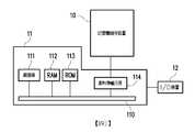
圖1是根據本發明的一範例實施例所繪示的主機系統、記憶體儲存裝置及輸入/輸出(I/O)裝置的示意圖。圖2是根據本發明的另一範例實施例所繪示的主機系統、記憶體儲存裝置及I/O裝置的示意圖。FIG. 1 is a schematic diagram of a host system, a memory storage device, and an input/output (I/O) device according to an exemplary embodiment of the present invention. 2 is a schematic diagram of a host system, a memory storage device, and an I/O device according to another exemplary embodiment of the present invention.
請參照圖1與圖2,主機系統11一般包括處理器111、隨機存取記憶體(random access memory, RAM)112、唯讀記憶體(read only memory, ROM)113及資料傳輸介面114。處理器111、隨機存取記憶體112、唯讀記憶體113及資料傳輸介面114皆耦接至系統匯流排(system bus)110。Referring to FIGS. 1 and 2, the
在本範例實施例中,主機系統11是透過資料傳輸介面114與記憶體儲存裝置10耦接。例如,主機系統11可經由資料傳輸介面114將資料儲存至記憶體儲存裝置10或從記憶體儲存裝置10中讀取資料。此外,主機系統11是透過系統匯流排110與I/O裝置12耦接。例如,主機系統11可經由系統匯流排110將輸出訊號傳送至I/O裝置12或從I/O裝置12接收輸入訊號。In the present exemplary embodiment, the
在本範例實施例中,處理器111、隨機存取記憶體112、唯讀記憶體113及資料傳輸介面114可設置在主機系統11的主機板20上。資料傳輸介面114的數目可以是一或多個。透過資料傳輸介面114,主機板20可以經由有線或無線方式耦接至記憶體儲存裝置10。記憶體儲存裝置10可例如是隨身碟201、記憶卡202、固態硬碟(Solid State Drive, SSD)203或無線記憶體儲存裝置204。無線記憶體儲存裝置204可例如是近距離無線通訊(Near Field Communication, NFC)記憶體儲存裝置、無線傳真(WiFi)記憶體儲存裝置、藍牙(Bluetooth)記憶體儲存裝置或低功耗藍牙記憶體儲存裝置(例如,iBeacon)等以各式無線通訊技術為基礎的記憶體儲存裝置。此外,主機板20也可以透過系統匯流排110耦接至全球定位系統(Global Positioning System, GPS)模組205、網路介面卡206、無線傳輸裝置207、鍵盤208、螢幕209、喇叭210等各式I/O裝置。例如,在一範例實施例中,主機板20可透過無線傳輸裝置207存取無線記憶體儲存裝置204。In the present exemplary embodiment, the
在一範例實施例中,所提及的主機系統為可實質地與記憶體儲存裝置配合以儲存資料的任意系統。雖然在上述範例實施例中,主機系統是以電腦系統來作說明,然而,圖3是根據本發明的另一範例實施例所繪示的主機系統與記憶體儲存裝置的示意圖。請參照圖3,在另一範例實施例中,主機系統31也可以是數位相機、攝影機、通訊裝置、音訊播放器、視訊播放器或平板電腦等系統,而記憶體儲存裝置30可為其所使用的SD卡32、CF卡33或嵌入式儲存裝置34等各式非揮發性記憶體儲存裝置。嵌入式儲存裝置34包括嵌入式多媒體卡(embedded MMC, eMMC)341及/或嵌入式多晶片封裝儲存裝置(embedded Multi Chip Package, eMCP)342等各類型將記憶體模組直接耦接於主機系統的基板上的嵌入式儲存裝置。In an exemplary embodiment, the mentioned host system is any system that can substantially cooperate with a memory storage device to store data. Although in the above exemplary embodiment, the host system is described as a computer system, however, FIG. 3 is a schematic diagram of a host system and a memory storage device according to another exemplary embodiment of the present invention. Referring to FIG. 3, in another exemplary embodiment, the
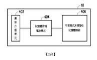
圖4是根據本發明的一範例實施例所繪示的記憶體儲存裝置的概要方塊圖。FIG. 4 is a schematic block diagram of a memory storage device according to an exemplary embodiment of the invention.
請參照圖4,記憶體儲存裝置10包括連接介面單元402、記憶體控制電路單元404與可複寫式非揮發性記憶體模組406。4, the
在本範例實施例中,連接介面單元402是相容於序列先進附件(Serial Advanced Technology Attachment, SATA)標準。然而,必須瞭解的是,本發明不限於此,連接介面單元402亦可以是符合並列先進附件(Parallel Advanced Technology Attachment, PATA)標準、電氣和電子工程師協會(Institute of Electrical and Electronic Engineers, IEEE)1394標準、高速周邊零件連接介面(Peripheral Component Interconnect Express, PCI Express)標準、通用序列匯流排(Universal Serial Bus, USB)標準、安全數位(Secure Digital, SD)介面標準、超高速一代(Ultra High Speed-I, UHS-I)介面標準、超高速二代(Ultra High Speed-II, UHS-II)介面標準、記憶棒(Memory Stick, MS)介面標準、多晶片封裝(Multi-Chip Package)介面標準、多媒體儲存卡(Multi Media Card, MMC)介面標準、崁入式多媒體儲存卡(Embedded Multimedia Card, eMMC)介面標準、通用快閃記憶體(Universal Flash Storage, UFS)介面標準、嵌入式多晶片封裝(embedded Multi Chip Package, eMCP)介面標準、小型快閃(Compact Flash, CF)介面標準、整合式驅動電子介面(Integrated Device Electronics, IDE)標準或其他適合的標準。連接介面單元402可與記憶體控制電路單元404封裝在一個晶片中,或者連接介面單元402是佈設於一包含記憶體控制電路單元404之晶片外。In this exemplary embodiment, the
記憶體控制電路單元404用以執行以硬體型式或韌體型式實作的多個邏輯閘或控制指令並且根據主機系統11的指令在可複寫式非揮發性記憶體模組406中進行資料的寫入、讀取與抹除等運作。The memory
可複寫式非揮發性記憶體模組406是耦接至記憶體控制電路單元404並且用以儲存主機系統11所寫入之資料。可複寫式非揮發性記憶體模組406可以是單階記憶胞(Single Level Cell, SLC)NAND型快閃記憶體模組(即,一個記憶胞中可儲存1個位元的快閃記憶體模組)、多階記憶胞(Multi Level Cell, MLC)NAND型快閃記憶體模組(即,一個記憶胞中可儲存2個位元的快閃記憶體模組)、複數階記憶胞(Triple Level Cell,TLC)NAND型快閃記憶體模組(即,一個記憶胞中可儲存3個位元的快閃記憶體模組)、其他快閃記憶體模組或其他具有相同特性的記憶體模組。The rewritable
可複寫式非揮發性記憶體模組406中的記憶胞是以陣列的方式設置。以下以二維陣列來對記憶胞陣列進行說明。但是,在此須注意的是,以下範例實施例只是記憶胞陣列的一種範例,在其他的範例實施例中,記憶胞陣列的配置方式可以被調整以符合實務上的需求。The memory cells in the rewritable
圖5是根據一範例實施例所繪示的可複寫式非揮發性記憶體模組的概要方塊圖。圖6是根據一範例實施例所繪示的記憶胞陣列的示意圖。FIG. 5 is a schematic block diagram of a rewritable non-volatile memory module according to an exemplary embodiment. FIG. 6 is a schematic diagram of a memory cell array according to an exemplary embodiment.
請同時參照圖5與圖6,可複寫式非揮發性記憶體模組406包括記憶胞陣列2202、字元線控制電路2204、位元線控制電路2206、行解碼器(column decoder)2208、資料輸入/輸出緩衝器2210與控制電路2212。5 and 6 at the same time, the rewritable
在本範例實施例中,記憶胞陣列2202可包括用以儲存資料的多個記憶胞502、多個選擇閘汲極(select gate drain, SGD)電晶體512與多個選擇閘源極(select gate source, SGS)電晶體514、以及連接此些記憶胞的多條位元線504、多條字元線506、與共用源極線508(如圖6所示)。記憶胞502是以陣列方式(或立體堆疊的方式)配置在位元線504與字元線506的交叉點上。當從記憶體控制電路單元404接收到寫入指令或讀取指令時,控制電路2212會控制字元線控制電路2204、位元線控制電路2206、行解碼器2208、資料輸入/輸出緩衝器2210來寫入資料至記憶胞陣列2202或從記憶胞陣列2202中讀取資料,其中字元線控制電路2204用以控制施予至字元線506的電壓,位元線控制電路2206用以控制施予至位元線504的電壓,行解碼器2208依據指令中的列位址以選擇對應的位元線,並且資料輸入/輸出緩衝器2210用以暫存資料。In this exemplary embodiment, the
可複寫式非揮發性記憶體模組406中的記憶胞是以臨界電壓的改變來儲存多位元(bits)。具體來說,每一個記憶胞的控制閘極(control gate)與通道之間有一個電荷捕捉層。透過施予一寫入電壓至控制閘極,可以改變電荷補捉層的電子量,因而改變了記憶胞的臨界電壓。此改變臨界電壓的程序亦稱為“把資料寫入至記憶胞”或“程式化記憶胞”。隨著臨界電壓的改變,記憶胞陣列2202的每一記憶胞具有多個儲存狀態。並且透過讀取電壓可以判斷記憶胞是屬於哪一個儲存狀態,藉此取得記憶胞所儲存的位元。The memory cells in the rewritable
圖7是根據一範例實施例所繪示儲存於記憶胞陣列中的寫入資料所對應的閘極電壓的統計分配圖。FIG. 7 is a statistical distribution diagram of gate voltages corresponding to write data stored in a memory cell array according to an exemplary embodiment.
請參照圖7,以MLC NAND型快閃記憶體為例,隨著不同的臨界電壓,每一記憶胞具有4種儲存狀態,並且此些儲存狀態分別地代表"11"、"10"、"00"與"01"等位元。換言之,每一個儲存狀態包括最低有效位元(Least Significant Bit,LSB)以及最高有效位元(Most Significant Bit,MSB)。在本範例實施例中,儲存狀態(即,"11"、"10"、"00"與"01")中從左側算起之第1個位元為LSB,而從左側算起之第2個位元為MSB。因此,在此範例實施例中,每一記憶胞可儲存2個位元。必須瞭解的是,圖7所繪示的臨界電壓及其儲存狀態的對應僅為一個範例。在本發明另一範例實施例中,臨界電壓與儲存狀態的對應亦可是隨著臨界電壓越大而以"11"、"10"、"01"與"00"排列,或是其他排列。此外,在另一範例實施例中,亦可定義從左側算起之第1個位元為MSB,而從左側算起之第2個位元為LSB。Please refer to FIG. 7, taking MLC NAND flash memory as an example, with different threshold voltages, each memory cell has 4 storage states, and these storage states respectively represent "11", "10", " "00" and "01" are equivalent. In other words, each storage state includes the least significant bit (Least Significant Bit, LSB) and the most significant bit (Most Significant Bit, MSB). In this exemplary embodiment, the first bit from the left in the storage state (ie, "11", "10", "00", and "01") is the LSB, and the second bit from the left The bits are MSB. Therefore, in this exemplary embodiment, each memory cell can store 2 bits. It must be understood that the correspondence between the threshold voltage and the storage state shown in FIG. 7 is only an example. In another exemplary embodiment of the present invention, the correspondence between the threshold voltage and the storage state may also be arranged in "11", "10", "01", and "00" as the threshold voltage increases, or other arrangements. In addition, in another exemplary embodiment, the first bit from the left side may be defined as the MSB, and the second bit from the left side is the LSB.
在一個記憶胞可以儲存多個位元(例如,MLC或TLC NAND快閃記憶體模組)的範例實施例中,屬於同一條字元線的實體程式化單元至少可被分類為下實體程式化單元與上實體程式化單元。例如,在MLC NAND快閃記憶體模組中,一記憶胞的最低有效位元(Least Significant Bit,LSB)是屬於下實體程式化單元,並且此記憶胞的最高有效位元(Most Significant Bit,MSB)是屬於上實體程式化單元。在一範例實施例中,下實體程式化單元亦稱為快頁(fast page),而上實體程式化單元亦稱為慢頁(slow page)。此外,在TLC NAND快閃記憶體模組中,一記憶胞的最低有效位元(Least Significant Bit,LSB)是屬於下實體程式化單元,此記憶胞的中間有效位元(Center Significant Bit,CSB)是屬於中實體程式化單元,並且此記憶胞的最高有效位元(Most Significant Bit,MSB)是屬於上實體程式化單元。In an exemplary embodiment in which one memory cell can store multiple bits (for example, MLC or TLC NAND flash memory modules), the physical programming units that belong to the same word line can be at least classified as lower physical programming Units and upper physical programming units. For example, in the MLC NAND flash memory module, the least significant bit (LSB) of a memory cell belongs to the lower physical programming unit, and the most significant bit of the memory cell (Most Significant Bit, MSB) belongs to the upper physical programming unit. In an exemplary embodiment, the lower physical programming unit is also called a fast page, and the upper physical programming unit is also called a slow page. In addition, in the TLC NAND flash memory module, the least significant bit (LSB) of a memory cell belongs to the lower physical programming unit, and the middle significant bit (Center Significant Bit, CSB) of this memory cell ) Belongs to the middle physical programming unit, and the most significant bit (MSB) of this memory cell belongs to the upper physical programming unit.
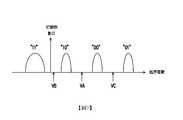
圖8是根據一範例實施例所繪示的從記憶胞中讀取資料的示意圖,其是以MLC NAND型快閃記憶體為例。FIG. 8 is a schematic diagram of reading data from a memory cell according to an exemplary embodiment, which uses MLC NAND flash memory as an example.
請參照圖8,記憶胞陣列2202之記憶胞的讀取運作是藉由施予讀取電壓VA~VC於控制閘極,藉由記憶胞通道的導通狀態,來識別記憶胞儲存之資料。驗證位元(VA)是用以指示施予讀取電壓VA時記憶胞通道是否為導通;驗證位元(VC)是用以指示施予讀取電壓VC時,記憶胞通道是否為導通;驗證位元(VB)是用以指示施予讀取電壓VB時,記憶胞通道是否為導通。在此假設驗證位元是“1”時表示對應的記憶胞通道導通,而驗證位元是“0”時表示對應的記憶胞通道沒有導通。如圖8所示,透過驗證位元(VA)~(VC)可以判斷記憶胞是處於哪一個儲存狀態,進而取得所儲存的位元。Referring to FIG. 8, the reading operation of the memory cells of the
圖9是根據另一範例實施例所繪示的從記憶胞中讀取資料的示意圖。9 is a schematic diagram of reading data from a memory cell according to another exemplary embodiment.
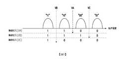
請參照圖9,以一TLC NAND型快閃記憶體為例,每一個儲存狀態包括左側算起之第1個位元的最低有效位元LSB、從左側算起之第2個位元的中間有效位元(Center Significant Bit,CSB)以及從左側算起之第3個位元的最高有效位元MSB。在此範例中,依照不同的臨界電壓,記憶胞具有8種儲存狀態(即,"111"、"110"、"100"、"101"、"001"、"000"、"010"與"011")。藉由施加讀取電壓VA~VG於控制閘極,可以識別記憶胞所儲存的位元。Please refer to FIG. 9, taking a TLC NAND flash memory as an example, each storage state includes the least significant bit LSB of the first bit from the left and the middle of the second bit from the left Center Significant Bit (CSB) and the MSB of the third most significant bit from the left. In this example, according to different threshold voltages, the memory cell has 8 storage states (ie, "111", "110", "100", "101", "001", "000", "010" and " 011"). By applying the reading voltages VA~VG to the control gate, the bits stored in the memory cell can be identified.
其中,值得說明的是,圖9的8種儲存狀態之排列順序,可依製造商之設計而訂,非以本範例之排列方式為限。Among them, it is worth noting that the arrangement order of the eight storage states in FIG. 9 can be customized according to the manufacturer's design, and is not limited to the arrangement in this example.
此外,可複寫式非揮發性記憶體模組406的記憶胞會構成多個實體程式化單元,並且此些實體程式化單元會構成多個實體抹除單元。具體而言,圖6中同一條字元線上的記憶胞會組成一或多個實體程式化單元。例如,若可複寫式非揮發性記憶體模組406為MLC NAND型快閃記憶體模組,則同一條字元線與多條位元線之交錯處上的記憶胞會構成2個實體程式化單元,亦即上實體程式化單元與下實體程式化單元。而一個上實體程式化單元與一個下實體程式化單元可以統稱為一實體程式化單元組。特別是,倘若欲讀取的資料位在一實體程式化單元組的一下實體程式化單元時,可以採用如圖8中的讀取電壓VA來識別此下實體程式化單元中每一位元的值。倘若欲讀取的資料位在一實體程式化單元組的一上實體程式化單元時,可以採用如圖8中讀取電壓VB與讀取電壓VC來識別此上實體程式化單元中每一位元的值。In addition, the memory cells of the rewritable
或者,若可複寫式非揮發性記憶體模組406為TLC NAND型快閃記憶體模組,則同一條字元線與多條位元線之交錯處上的記憶胞會構成3個實體程式化單元,亦即上實體程式化單元、中實體程式化單元與下實體程式化單元。而一個上實體程式化單元、一個中實體程式化單元與一個下實體程式化單元可以統稱為一實體程式化單元組。特別是,倘若欲讀取的資料位在一實體程式化單元組的一下實體程式化單元時,可以採用如圖9中的讀取電壓VA來識別此下實體程式化單元中每一位元的值。倘若欲讀取的資料位在一實體程式化單元組的一中實體程式化單元時,可以採用如圖9中的讀取電壓VB與讀取電壓VC來識別此中實體程式化單元中每一位元的值。倘若欲讀取的資料位在一實體程式化單元組的一上實體程式化單元時,可以採用如圖9中的讀取電壓VD、讀取電壓VE、讀取電壓VF與讀取電壓VG來識別此上實體程式化單元中每一位元的值。Or, if the rewritable
在本範例實施例中,實體程式化單元為程式化的最小單元。即,實體程式化單元為寫入資料的最小單元。例如,實體程式化單元為實體頁面(page)或是實體扇(sector)。若實體程式化單元為實體頁面,則此些實體程式化單元通常包括資料位元區與冗餘(redundancy)位元區。資料位元區包含多個實體扇,用以儲存使用者資料,而冗餘位元區用以儲存系統資料(例如,錯誤更正碼)。在本範例實施例中,資料位元區包含32個實體扇,且一個實體扇的大小為512位元組(byte, B)。然而,在其他範例實施例中,資料位元區中也可包含8個、16個或數目更多或更少的實體扇,並且每一個實體扇的大小也可以是更大或更小。另一方面,實體抹除單元為抹除之最小單位。亦即,每一實體抹除單元含有最小數目之一併被抹除之記憶胞。例如,實體抹除單元為實體區塊(block)。In this exemplary embodiment, the physical programming unit is the smallest unit of programming. That is, the physical programming unit is the smallest unit to write data. For example, the physical stylization unit is a physical page or a sector. If the physical programming unit is a physical page, these physical programming units usually include a data bit area and a redundancy bit area. The data bit area includes multiple physical fans to store user data, and the redundant bit area is used to store system data (eg, error correction codes). In this exemplary embodiment, the data bit area includes 32 physical fans, and the size of one physical fan is 512 bytes (byte, B). However, in other exemplary embodiments, the data bit area may also include 8, 16 or more or fewer physical fans, and the size of each physical fan may also be larger or smaller. On the other hand, the physical erasing unit is the smallest unit of erasing. That is, each physical erasing unit contains one of the minimum number of memory cells to be erased. For example, the physical erasing unit is a physical block.
圖10是根據本範例實施例所繪示之實體抹除單元的範例示意圖。FIG. 10 is an exemplary schematic diagram of a physical erasing unit according to this exemplary embodiment.
請參照圖10,在本範例實施例中,假設一個實體抹除單元是由多個實體程式化單元組所組成,其中每個實體程式化單元組包括由排列在同一條字元線上的數個記憶胞所組成的下實體程式化單元、中實體程式化單元與上實體程式化單元。例如,在實體抹除單元中,屬於下實體程式化單元的第0個實體程式化單元、屬於中實體程式化單元的第1個實體程式化單元和屬於上實體程式化單元的第2個實體程式化單元會被視為一個實體程式化單元組。類似地,第3、4、5個實體程式化單元會被視為一個實體程式化單元組,並且以此類推其他實體程式化單元亦是依據此方式被區分為多個實體程式化單元組。Referring to FIG. 10, in this exemplary embodiment, it is assumed that a physical erasing unit is composed of multiple physical stylized unit groups, where each physical stylized unit group includes several arranged on the same character line The memory cell consists of a lower physical programming unit, a middle physical programming unit and an upper physical programming unit. For example, in the physical erasing unit, the 0th physical programming unit belonging to the lower physical programming unit, the 1st physical programming unit belonging to the middle physical programming unit, and the 2nd entity belonging to the upper physical programming unit The stylized unit will be regarded as a group of physical stylized units. Similarly, the 3rd, 4th, and 5th physical stylized units will be regarded as one physical stylized unit group, and other physical stylized units can be divided into multiple physical stylized unit groups in this way.
圖11是根據本發明的一範例實施例所繪示的記憶體控制電路單元的概要方塊圖。FIG. 11 is a schematic block diagram of a memory control circuit unit according to an exemplary embodiment of the present invention.
請參照圖11,記憶體控制電路單元404包括記憶體管理電路702、主機介面704、記憶體介面706及錯誤檢查與校正電路708。Referring to FIG. 11, the memory
記憶體管理電路702用以控制記憶體控制電路單元404的整體運作。具體來說,記憶體管理電路702具有多個控制指令,並且在記憶體儲存裝置10運作時,此些控制指令會被執行以進行資料的寫入、讀取與抹除等運作。以下說明記憶體管理電路702或任何包含於記憶體控制電路單元404中的電路元件之操作時,等同於說明記憶體控制電路單元404的操作。The
在本範例實施例中,記憶體管理電路702的控制指令是以韌體型式來實作。例如,記憶體管理電路702具有微處理器單元(未繪示)與唯讀記憶體(未繪示),並且此些控制指令是被燒錄至此唯讀記憶體中。當記憶體儲存裝置10運作時,此些控制指令會由微處理器單元來執行以進行資料的寫入、讀取與抹除等運作。In the present exemplary embodiment, the control commands of the
在另一範例實施例中,記憶體管理電路702的控制指令亦可以程式碼型式儲存於可複寫式非揮發性記憶體模組406的特定區域(例如,記憶體模組中專用於存放系統資料的系統區)中。此外,記憶體管理電路702具有微處理器單元(未繪示)、唯讀記憶體(未繪示)及隨機存取記憶體(未繪示)。特別是,此唯讀記憶體具有開機碼(boot code),並且當記憶體控制電路單元404被致能時,微處理器單元會先執行此開機碼來將儲存於可複寫式非揮發性記憶體模組406中之控制指令載入至記憶體管理電路702的隨機存取記憶體中。之後,微處理器單元會運轉此些控制指令以進行資料的寫入、讀取與抹除等運作。In another exemplary embodiment, the control commands of the
此外,在另一範例實施例中,記憶體管理電路702的控制指令亦可以一硬體型式來實作。例如,記憶體管理電路702包括微控制器、記憶胞管理電路、記憶體寫入電路、記憶體讀取電路、記憶體抹除電路與資料處理電路。記憶胞管理電路、記憶體寫入電路、記憶體讀取電路、記憶體抹除電路與資料處理電路是耦接至微控制器。記憶胞管理電路用以管理可複寫式非揮發性記憶體模組406的記憶胞或其群組。記憶體寫入電路用以對可複寫式非揮發性記憶體模組406下達寫入指令序列以將資料寫入至可複寫式非揮發性記憶體模組406中。記憶體讀取電路用以對可複寫式非揮發性記憶體模組406下達讀取指令序列以從可複寫式非揮發性記憶體模組406中讀取資料。記憶體抹除電路用以對可複寫式非揮發性記憶體模組406下達抹除指令序列以將資料從可複寫式非揮發性記憶體模組406中抹除。資料處理電路用以處理欲寫入至可複寫式非揮發性記憶體模組406的資料以及從可複寫式非揮發性記憶體模組406中讀取的資料。寫入指令序列、讀取指令序列及抹除指令序列可各別包括一或多個程式碼或指令碼並且用以指示可複寫式非揮發性記憶體模組406執行相對應的寫入、讀取及抹除等操作。在一範例實施例中,記憶體管理電路702還可以下達其他類型的指令序列給可複寫式非揮發性記憶體模組406以指示執行相對應的操作。In addition, in another exemplary embodiment, the control commands of the
主機介面704是耦接至記憶體管理電路702並且用以接收與識別主機系統11所傳送的指令與資料。也就是說,主機系統11所傳送的指令與資料會透過主機介面704來傳送至記憶體管理電路702。在本範例實施例中,主機介面704是相容於SATA標準。然而,必須瞭解的是本發明不限於此,主機介面704亦可以是相容於PATA標準、IEEE 1394標準、PCI Express標準、USB標準、SD標準、UHS-I標準、UHS-II標準、MS標準、MMC標準、eMMC標準、UFS標準、CF標準、IDE標準或其他適合的資料傳輸標準。The
記憶體介面706是耦接至記憶體管理電路702並且用以存取可複寫式非揮發性記憶體模組406。也就是說,欲寫入至可複寫式非揮發性記憶體模組406的資料會經由記憶體介面706轉換為可複寫式非揮發性記憶體模組406所能接受的格式。具體來說,若記憶體管理電路702要存取可複寫式非揮發性記憶體模組406,記憶體介面706會傳送對應的指令序列。例如,這些指令序列可包括指示寫入資料的寫入指令序列、指示讀取資料的讀取指令序列、指示抹除資料的抹除指令序列、以及用以指示各種記憶體操作(例如,改變讀取電壓準位或執行垃圾回收程序等等)的相對應的指令序列。這些指令序列例如是由記憶體管理電路702產生並且透過記憶體介面706傳送至可複寫式非揮發性記憶體模組406。這些指令序列可包括一或多個訊號,或是在匯流排上的資料。這些訊號或資料可包括指令碼或程式碼。例如,在讀取指令序列中,會包括讀取的辨識碼、記憶體位址等資訊。The
錯誤檢查與校正電路708是耦接至記憶體管理電路702並且用以執行錯誤檢查與校正程序以確保資料的正確性。具體來說,當記憶體管理電路702從主機系統11中接收到寫入指令時,錯誤檢查與校正電路708會為對應此寫入指令的資料產生對應的錯誤更正碼(error correcting code, ECC)及/或錯誤檢查碼(error detecting code,EDC),並且記憶體管理電路702會將對應此寫入指令的資料與對應的錯誤更正碼及/或錯誤檢查碼寫入至可複寫式非揮發性記憶體模組406中。之後,當記憶體管理電路702從可複寫式非揮發性記憶體模組406中讀取資料時會同時讀取此資料對應的錯誤更正碼及/或錯誤檢查碼,並且錯誤檢查與校正電路708會依據此錯誤更正碼及/或錯誤檢查碼對所讀取的資料執行錯誤檢查與校正程序。The error check and
在一範例實施例中,記憶體控制電路單元404還包括緩衝記憶體710與電源管理電路712。In an exemplary embodiment, the memory
緩衝記憶體710是耦接至記憶體管理電路702並且用以暫存來自於主機系統11的資料與指令或來自於可複寫式非揮發性記憶體模組406的資料。電源管理電路712是耦接至記憶體管理電路702並且用以控制記憶體儲存裝置10的電源。The
在本範例實施例中,錯誤檢查與校正電路708可以針對儲存於同一個實體程式化單元中的資料進行單框架(single-frame)編碼,也可以針對儲存於多個實體程式化單元中的資料進行多框架(multi-frame)編碼。單框架編碼與多框架編碼可以分別採用低密度奇偶檢查校正碼(low density parity code,LDPC)、BCH碼、迴旋碼(convolutional code)或渦輪碼(turbo code)等編碼演算法的至少其中之一。或者,在一範例實施例中,多框架編碼還可以採用里德-所羅門碼(Reed-solomon codes, RS codes)演算法或互斥或(XOR)演算法。此外,在另一範例實施例中,更多未列於上的編碼演算法也可以被採用,在此便不贅述。根據所採用的編碼演算法,錯誤檢查與校正電路708可以編碼欲保護之資料來產生相對應的錯誤更正碼及/或錯誤檢查碼。為了說明方便,以下將經由編碼產生的錯誤更正碼及/或錯誤檢查碼統稱為編碼資料。圖12是根據本發明的一範例實施例所繪示的多框架編碼的示意圖。In this exemplary embodiment, the error checking and
請參照圖12,以編碼實體程式化單元810(0)~810(E)所儲存之資料來產生相對應的編碼資料820為例,實體程式化單元810(0)~810(E)中的每一者所儲存之至少部分資料可視為一個框架。在多框架編碼中,是以每一個位元(或,位元組)所在的位置為依據來對實體程式化單元810(0)~810(E)中的資料進行編碼。例如,位於位置801(1)的位元b11、b21、…、bp1會被編碼為編碼資料820中的位元bo1,位於位置801(2)的位元b12、b22、…、bp2會被編碼為編碼資料820中的位元bo2;以此類推,位於位置801(r)的位元b1r、b2r、…、bpr會被編碼為編碼資料820中的位元bor。爾後,根據編碼資料820即可對從實體程式化單元810(0)~810(E)中讀取的資料進行解碼,以嘗試更正所讀取之資料中可能存在的錯誤。Referring to FIG. 12, taking the data stored in the encoding physical programming units 810(0)~810(E) to generate corresponding encoded
此外,在圖12的另一範例實施例中,用於產生編碼資料820的資料也可能包括實體程式化單元810(0)~810(E)所儲存之資料中的資料位元(data bits)所對應的冗餘位元(redundancy bits)。以實體程式化單元810(0)所儲存之資料為例,其中的冗餘位元例如是對儲存於實體程式化單元810(0)中的資料位元進行單框架編碼而產生的。在本範例實施例中,假設在讀取實體程式化單元810(0)中的資料時,從實體程式化單元810(0)中讀取出的資料可以先使用實體程式化單元810(0)中的冗餘位元(例如,單框架編碼的編碼資料)來解碼以進行錯誤偵測與更正。然而,當使用實體程式化單元810(0)中的冗餘位元進行解碼發生失敗(例如,解碼後實體程式化單元810(0)中所儲存的資料的錯誤位元數大於一門檻值)時,可以使用重新讀取(Retry-Read)機制嘗試從實體程式化單元810(0)中讀取出正確的資料。關於重新讀取機制的細節請容後詳述。而當無法藉由重新讀取(Retry-Read)機制從實體程式化單元810(0)中讀取出正確的資料時,可以讀取編碼資料820以及實體程式化單元810(1)~810(E)的資料,並根據編碼資料820以及實體程式化單元810(1)~810(E)的資料進行解碼,以嘗試更正實體程式化單元810(0)中所儲存的資料中存在的錯誤。也就是說,在本範例實施例中,當使用單框架編碼產生的編碼資料進行解碼發生失敗以及使用重新讀取(Retry-Read)機制進行讀取發生失敗時,會改用多框架編碼產生的編碼資料進行解碼。In addition, in another exemplary embodiment of FIG. 12, the data used to generate the encoded
特別是,圖13是根據一範例實施例繪示重新讀取機制的示意圖。In particular, FIG. 13 is a schematic diagram illustrating a re-reading mechanism according to an exemplary embodiment.
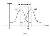
請參照圖13,在此以SLC快閃記憶體為例,分佈1410與分佈1420是用來表示多個第一記憶胞的儲存狀態,而分佈1410與1420分別代表著不同的儲存狀態。這些第一記憶胞可以屬於同樣的實體程式化單元或是不同的實體程式化單元,本發明並不在此限。在此假設當一個記憶胞屬於分佈1410時,此記憶胞所儲存的是位元“1”;當記憶胞屬於分佈1420時,此記憶胞儲存的是位元“0”。當記憶體管理電路702以讀取電壓1440來讀取記憶胞時,記憶體管理電路702會取得驗證位元,其是用來指示此記憶胞是否為導通。在此假設記憶胞導通時驗證位元是“1”,反之則是 “0”,但本發明並不在此限。若此驗證位元為 “1”,則記憶體管理電路702會判斷此記憶胞屬於分佈1410,反之則是分佈1420。然而,分佈1410與分佈1420在區域1430中是重疊的。也就是說,有若干個記憶胞應該是屬於分佈1410但被辨識為分佈1420,並且有若干個記憶胞應該是屬於分佈1420但被辨識為分佈1410。Please refer to FIG. 13, here taking SLC flash memory as an example, the
在此範例實施例中,當要讀取這些記憶胞時,記憶體管理電路702會先選擇一預設的讀取電壓(例如,讀取電壓1441)來讀取這些記憶胞以取得這些記憶胞的驗證位元。錯誤檢查與校正電路708會根據這些記憶胞的驗證位元來執行解碼操作,以產生多個解碼位元,而此些解碼位元可以組成一個解碼後的資料(亦稱為,碼字)。In this exemplary embodiment, when the memory cells are to be read, the
若解碼失敗,表示這些記憶胞儲存有不可更正的錯誤位元。若解碼失敗,在重新讀取機制中,記憶體管理電路702會重新取得另一讀取電壓,並用此另一讀取電壓(例如讀取電壓1442)來讀取這些第一記憶胞,以重新取得記憶胞的驗證位元。記憶體管理電路702會根據重新取得的驗證位元來執行上述的解碼操作以取得由多個解碼位元組成的另一解碼後的資料。在一範例實施例中,錯誤檢查與校正電路708會根據該另一解碼後的資料所對應的校驗子判斷所述另一解碼後的資料是否為有效的碼字。若所述另一解碼後的資料非為有效的碼字時,記憶體管理電路702會判斷解碼失敗。若重新取得讀取電壓的次數沒有超過預設次數,則記憶體管理電路702會再重新取得其他取得電壓(例如,讀取電壓1443),並且根據重新取得的讀取電壓1443讀取記憶胞,以重新取得驗證位元並執行第一解碼操作。If the decoding fails, it means that these memory cells have stored uncorrectable error bits. If decoding fails, in the re-reading mechanism, the
換句話說,當有不可更正的錯誤位元時,透過重新取得讀取電壓,一些記憶胞的驗證位元會被改變,進而有機會改變解碼操作的解碼結果。邏輯上來說,上述重新取得讀取電壓的動作是要翻轉(flip)一個碼字中的若干位元,並對新的碼字重新解碼。在一些情況下,在翻轉前無法解碼的碼字(有不可更正的錯誤位元),有可能在翻轉後可以解碼。並且,在一範例實施例中記憶體管理電路702會嘗試解碼數次,直到嘗試的次數超過預設次數為止。然而,本發明並不限制預設次數為多少。In other words, when there are uncorrectable erroneous bits, by re-acquiring the read voltage, the verification bits of some memory cells will be changed, and there is a chance to change the decoding result of the decoding operation. Logically speaking, the above-mentioned action of regaining the read voltage is to flip several bits in a code word and re-decode the new code word. In some cases, codewords (with uncorrectable error bits) that cannot be decoded before flipping may be decoded after flipping. Moreover, in an exemplary embodiment, the
需說明的是,使用單框架編碼所產生的編碼資料所執行的解碼操作可以分成硬位元(hard bit mode)模式解碼與軟位元模式(soft bit mode)解碼。在硬位元模式解碼與軟位元模式解碼的過程中,均需根據記憶胞的「解碼初始值」來進行解碼。在硬位元模式解碼的過程中,記憶胞的解碼初始值是根據一個驗證位元而被分為兩個數值(例如,n與-n)。例如,若驗證位元是”1”,記憶體管理電路702會設定對應的記憶胞的解碼初始值為-n;若驗證位元是”0”,則解碼初始值為n。其中n為正數,但本發明並不限制正整數n的值為多少。也就是說,根據兩種數值來執行的疊代解碼亦被稱為硬位元模式(hard bit mode)解碼。然而,上述改變讀取電壓的步驟也可以應用在軟位元模式(soft bit mode)解碼,其中每一個記憶胞的解碼初始值是根據多個驗證位元所決定。值得注意的是,不論是硬位元模式或是軟位元模式,在疊代解碼中都會計算位元的機率值,因此都屬於機率解碼演算法。而硬位元模式解碼與軟位元模式解碼的詳細執行過程可以由習知技術而得知,在此不再贅述。It should be noted that the decoding operation performed by using the encoded data generated by the single frame encoding can be divided into hard bit mode decoding and soft bit mode decoding. In the process of hard bit mode decoding and soft bit mode decoding, both need to be decoded according to the "decoding initial value" of the memory cell. In the decoding process of the hard bit mode, the initial decoding value of the memory cell is divided into two values (for example, n and -n) according to one verification bit. For example, if the verification bit is "1", the
值得注意的是,在圖13中所舉的是SLC快閃記憶體的例子,但重新取得讀取電壓的步驟也可以適用於MLC或是TLC快閃記憶體。如圖8所示,改變讀取電壓VA會翻轉一個記憶胞的LSB,而改變讀取電壓VB或VC則可以翻轉一個記憶胞的MSB。因此,改變讀取電壓VA、VB或VC都可以將一個碼字改變為另一個碼字。改變碼字的結果也適用於圖9的TLC快閃記憶體。本發明並不限制所使用的是SLC、MLC或是TLC快閃記憶體。需說明的是,讀取電壓VA~VC可以統稱為一個讀取電壓組。而記憶體管理電路702例如可以從多個讀取電壓組中挑選出某一組讀取電壓組來讀取記憶胞。It is worth noting that the example of SLC flash memory is given in FIG. 13, but the step of regaining the read voltage can also be applied to MLC or TLC flash memory. As shown in FIG. 8, changing the reading voltage VA will flip the LSB of a memory cell, and changing the reading voltage VB or VC may flip the MSB of a memory cell. Therefore, changing the reading voltage VA, VB or VC can change one codeword to another codeword. The result of changing the code word also applies to the TLC flash memory of FIG. 9. The invention does not limit the use of SLC, MLC or TLC flash memory. It should be noted that the reading voltages VA~VC can be collectively referred to as a reading voltage group. The
在此需說明的是,在本實施例中,當欲讀取可複寫式非揮發性記憶體模組406中的一實體程式化單元時,記憶體管理電路702會先使用一預設電壓組來讀取該實體程式化單元並根據使用此預設電壓組讀取出的資料執行硬位元模式解碼。當解碼發生失敗時,會執行前述的重新讀取機制以再次地執行硬位元模式解碼。當重新讀取(Retry-Read)機制進行讀取發生失敗時,記憶體管理電路702會執行軟位元模式解碼。當軟位元模式解碼發生失敗時,記憶體管理電路702會改用多框架編碼產生的編碼資料進行解碼。It should be noted that in this embodiment, when a physical programming unit in the rewritable
需注意的是,當對一個讀取指令所讀取出的資料執行解碼操作但發生解碼失敗而反覆地執行解碼操作(例如,重新讀取機制)時,在該讀取指令後續的讀取指令都需被迫等待而無法被執行,此情況會導致讀取指令的執行效率低落。It should be noted that when the decoding operation is performed on the data read by a read command but the decoding fails and the decoding operation is repeatedly executed (for example, a re-reading mechanism), the subsequent read command All have to be forced to wait and cannot be executed. This situation will lead to inefficient execution of read instructions.
因此,本發明提出一種解碼方法,當某一個讀取指令(亦稱為,第一讀取指令)用以從一實體程式化單元(亦稱為,第一實體程式化單元)中讀取出資料時,若讀取的過程中所執行的部分的重新讀取機制皆發生失敗時,記憶體管理電路702會先暫停執行對從第一實體程式化單元中讀取出的資料的解碼,並且會先執行第一讀取指令後續的其他指令(例如,讀取指令)。在執行後續的其他指令後,記憶體管理電路702會再返回執行根據第一讀取指令進行讀取並對第一讀取指令所讀取出的資料執行另一部分的重新讀取機制。Therefore, the present invention proposes a decoding method, when a certain read command (also called, first read command) is used to read from a physical programming unit (also called, first physical programming unit) During data reading, if all the re-reading mechanisms performed during the reading process fail, the
更詳細來說,圖14是根據一範例實施例所繪示用於重新讀取機制的多個讀取電壓組的示意圖。請參照圖14,假設記憶體管理電路702從主機系統11接收多個指令時。在此假設此些指令中包括一第一讀取指令,且第一讀取指令以外的其他指令也皆為讀取指令。然而在其他實施例中,前述第一讀取指令以外的其他指令也可以是其他的指令(例如,寫入指令、抹除指令、垃圾收集指令或區塊損耗平衡指令等,本發明對此不做限制)。假設此些讀取指令中的第一讀取指令用於讀取第一實體程式化單元。首先,記憶體管理電路702會先使用預設電壓組(未繪示)來讀取該第一實體程式化單元並根據使用此預設電壓組讀取出的資料執行硬位元模式解碼。當解碼發生失敗時,記憶體管理電路702會執行重新讀取機制以選擇如圖14中的讀取電壓組G1,並根據讀取電壓組G1中的讀取電壓V1~V1n讀取第一實體程式化單元以獲得使用讀取電壓V1~V1n所讀取出的資料。之後,記憶體管理電路702會對使用讀取電壓V1~V1n所讀取出的資料再次地執行硬位元模式解碼。In more detail, FIG. 14 is a schematic diagram illustrating a plurality of read voltage groups for a re-reading mechanism according to an exemplary embodiment. Referring to FIG. 14, assume that the
當對使用讀取電壓V1~V1n所讀取出的資料執行硬位元模式解碼發生失敗時,記憶體管理電路702會執行重新讀取機制以選擇如圖14中的讀取電壓組G2,並根據讀取電壓組G2中的讀取電壓V2~V2n讀取第一實體程式化單元以獲得使用讀取電壓V2~V2n所讀取出的資料。之後,記憶體管理電路702會對使用讀取電壓V2~V2n所讀取出的資料再次地執行硬位元模式解碼。When the hard-bit mode decoding of the data read using the read voltages V1~V1n fails, the
當對使用讀取電壓V2~V2n所讀取出的資料執行硬位元模式解碼發生失敗時,記憶體管理電路702會選擇如圖14中的讀取電壓組G3,並根據讀取電壓組G3中的讀取電壓V3~V3n讀取第一實體程式化單元以獲得使用讀取電壓V3~V3n所讀取出的資料。之後,記憶體管理電路702會對使用讀取電壓V3~V3n所讀取出的資料再次地執行硬位元模式解碼。When the hard bit mode decoding of the data read using the read voltages V2~V2n fails, the
當對使用讀取電壓V3~V3n所讀取出的資料執行硬位元模式解碼發生失敗時,記憶體管理電路702會執行重新讀取機制以選擇如圖14中的讀取電壓組G4,並根據讀取電壓組G4中的讀取電壓V4~V4n讀取第一實體程式化單元以獲得使用讀取電壓V4~V4n所讀取出的資料。之後,記憶體管理電路702會對使用讀取電壓V4~V4n所讀取出的資料再次地執行硬位元模式解碼。When the hard bit mode decoding of the data read using the reading voltages V3~V3n fails, the
當對使用讀取電壓V4~V4n所讀取出的資料執行硬位元模式解碼發生失敗時,記憶體管理電路702會執行重新讀取機制以選擇如圖14中的讀取電壓組G5,並根據讀取電壓組G5中的讀取電壓V5~V5n讀取第一實體程式化單元以獲得使用讀取電壓V5~V5n所讀取出的資料。之後,記憶體管理電路702會對使用讀取電壓V5~V5n所讀取出的資料再次地執行硬位元模式解碼。When the hard-bit mode decoding of the data read using the reading voltages V4~V4n fails, the
當對使用讀取電壓V5~V5n所讀取出的資料執行硬位元模式解碼發生失敗時,此時記憶體管理電路702會暫停執行前述的第一讀取指令,並且會執行在第一讀取指令後續的不同於第一讀取指令的至少一其他指令(亦稱為,第一其他指令)。在本實施例中,此第一其他指令的數量例如是三個。在本實施例中,假設第一讀取指令在所有的指令中是排序在第一個的指令,則前述的第一其他指令則是在所有的指令中排序為第二、第三與第四個的指令。然而本發明並不用於限定第一其他指令的數量。When the hard-bit mode decoding of the data read using the read voltages V5~V5n fails, the
在此需說明的是,前述讀取電壓組G1~G5可以統稱為「第一讀取電壓組」。而使用讀取電壓組G1~G5從第一實體程式化單元中所讀取出並且用以執行硬位元模式解碼的資料可以統稱為「第一資料」。硬位元模式解碼的操作可以稱為「第一解碼操作」。需注意的是,在本實施例中第一讀取電壓組的數量為五,然而在較佳的實施例中,第一讀取電壓組的數量為大於或等於五且小於或等於十。It should be noted here that the aforementioned read voltage groups G1 to G5 may be collectively referred to as "first read voltage group". The data read from the first physical programming unit using the read voltage groups G1~G5 and used to perform the hard bit mode decoding can be collectively referred to as "first data". The operation of hard bit mode decoding may be referred to as "first decoding operation". It should be noted that in this embodiment, the number of first read voltage groups is five, but in a preferred embodiment, the number of first read voltage groups is greater than or equal to five and less than or equal to ten.
假設在成功地執行第一其他指令後,記憶體管理電路702會返回執行第一讀取指令。更詳細來說,記憶體管理電路702會根據第一讀取指令,接續執行先前尚未執行完的重新讀取機制以選擇如圖14中的讀取電壓組G6(未繪示),並根據讀取電壓組G6中的讀取電壓讀取第一實體程式化單元並根據所讀取出的資料再次地執行硬位元模式解碼。Assume that after successfully executing the first other instruction, the
當對使用讀取電壓組G6所讀取出的資料進行解碼發生失敗時,記憶體管理電路702會再次地執行重新讀取機制。假設在後續的重新讀取機制中,記憶體管理電路702對使用讀取電壓組G7~G10(未繪示)所讀取出的資料(亦稱為,第二資料)執行硬位元模式解碼皆發生失敗時,記憶體管理電路702會暫停執行前述的第一讀取指令,並且會執行在前述第一其他指令後續的至少一第二其他指令。在本實施例中,第二其他指令的數量例如是三個。在本實施例中,假設第一其他指令是指所有指令中排序在第二個、第三個與第四個的指令,因此第二其他指令是所有指令中排序在第五個、第六個與第七個的指令。此外,讀取電壓組G6~G10可以統稱為「第二讀取電壓組」。在此需說明的是,第一其他指令與第二其他指令可以統稱為「不同於第一讀取指令之其他指令」。When the decoding of the data read using the read voltage group G6 fails, the
假設在成功地執行第二其他指令後,記憶體管理電路702例如會判斷在第一讀取指令後續被成功執行的指令的數量(即,已被執行的不同於第一讀取指令之其他指令的數量)是否達到門檻値。當已被執行的不同於第一讀取指令之其他指令的數量非大於門檻値時,若記憶體管理電路702再次執行一部分的重新讀取機制皆發生失敗時,記憶體管理電路702可以再次先暫停執行第一讀取指令並且先執行排序在前述第二其他指令後的多個指令。Assume that after successfully executing the second other instruction, the
然而,當已被執行的不同於第一讀取指令之其他指令的數量大於門檻値時,記憶體管理電路702返回執行第一讀取指令以將完整的解碼流程(例如,剩餘未執行的重新讀取機制與軟位元模式解碼)執行完畢。更詳細來說,記憶體管理電路702會根據第一讀取指令,接續執行前述尚未執行完的重新讀取機制以選擇如圖14中的讀取電壓組G11(未繪示),並根據讀取電壓組G11中的讀取電壓讀取第一實體程式化單元並根據所讀取出的資料再次地執行硬位元模式解碼。當對使用讀取電壓組G11所讀取出的資料進行解碼發生失敗時,記憶體管理電路702會再次地執行重新讀取機制。假設在後續的重新讀取機制中,記憶體管理電路702對使用讀取電壓組G12(未繪示)~GX所讀取出的資料執行硬位元模式解碼皆發生失敗時,記憶體管理電路702不會暫停執行前述的第一讀取指令而是根據第一讀取指令執行軟位元模式解碼(亦稱為,第二解碼操作)。更詳細來說,記憶體管理電路702例如可以使用其他讀取電壓組(未繪示)讀取第一實體程式化單元以獲得一資料(亦稱為,第四資料),並且對此第四資料執行軟位元模式解碼。However, when the number of other instructions that have been executed other than the first read instruction is greater than the threshold value, the
在此需說明的是,使用讀取電壓組G11~GX所讀取出的資料可以統稱為「第三資料」。It should be noted here that the data read using the reading voltage group G11~GX can be collectively referred to as "third data".
圖15是根據一範例實施例繪示解碼方法的流程圖。15 is a flowchart illustrating a decoding method according to an exemplary embodiment.
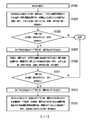
請參照圖15,在步驟S1501中,記憶體管理電路702接收多個指令。在步驟S1503中,記憶體管理電路702根據前述多個指令中的第一讀取指令,使用多個讀取電壓組中的多個第一讀取電壓組讀取第一實體程式化單元以分別獲得多個第一資料,並對此些第一資料中的每一個第一資料執行第一解碼操作。在步驟S1505中,記憶體管理電路702判斷所述多個第一資料的其中之一是否解碼成功。當所述多個第一資料的其中之一解碼成功時,則結束圖15的流程。當對所述多個第一資料中的每一個第一資料執行第一解碼操作皆發生失敗時,在步驟S1507中,記憶體管理電路702執行所述多個指令中不同於第一讀取指令的其他指令。之後在執行完不同於第一讀取指令的其他指令後,在步驟S1509中,記憶體管理電路702根據第一讀取指令,使用多個讀取電壓組中的多個第二讀取電壓組讀取第一實體程式化單元以分別獲得多個第二資料,並對此些第二資料中的每一個第二資料執行第一解碼操作。在步驟S1511中,記憶體管理電路702判斷所述多個第二資料的其中之一是否解碼成功。當所述多個第二資料的其中之一解碼成功時,會結束圖14的流程。當對所述多個第二資料中的每一個第二資料執行第一解碼操作皆發生失敗時,在步驟S1513中,記憶體管理電路702執行所述多個讀取指令中不同於第一讀取指令的其他指令。之後在步驟S1515中,當所述多個指令中已被執行的不同於第一讀取指令的其他指令的數量達到一門檻値時,記憶體管理電路702根據第一讀取指令使用所述多個讀取電壓組中的剩餘讀取電壓組讀取第一實體程式化單元以獲得第三資料,並對第三資料中執行第一解碼操作。Referring to FIG. 15, in step S1501, the
綜上所述,本發明的解碼方法、記憶體控制電路單元以及記憶體儲存裝置,可以在對某一個讀取指令所讀取出的資料執行部分的重新讀取機制且該些部分的重新讀取機制皆發生失敗時,先暫停執行對應於該讀取指令的解碼,並且先執行該讀取指令後續的其他指令,藉此避免後續的指令等待前一個讀取指令執行完整的解碼操作所花費的時間。In summary, the decoding method, memory control circuit unit, and memory storage device of the present invention can perform a partial re-reading mechanism on the data read by a certain read command and re-read those parts When all the fetch mechanisms fail, the execution of the decoding corresponding to the read instruction is suspended first, and other instructions subsequent to the read instruction are executed first, thereby avoiding the cost of subsequent instructions waiting for the previous read instruction to perform a complete decoding operation. time.
雖然本發明已以實施例揭露如上,然其並非用以限定本發明,任何所屬技術領域中具有通常知識者,在不脫離本發明的精神和範圍內,當可作些許的更動與潤飾,故本發明的保護範圍當視後附的申請專利範圍所界定者為準。Although the present invention has been disclosed as above with examples, it is not intended to limit the present invention. Any person with ordinary knowledge in the technical field can make some changes and modifications without departing from the spirit and scope of the present invention. The scope of protection of the present invention shall be subject to the scope defined in the appended patent application.
10‧‧‧記憶體儲存裝置10‧‧‧Memory storage device
11‧‧‧主機系統11‧‧‧Host system
110‧‧‧系統匯流排110‧‧‧System bus
111‧‧‧處理器111‧‧‧ processor
112‧‧‧隨機存取記憶體112‧‧‧ Random Access Memory
113‧‧‧唯讀記憶體113‧‧‧Read-only memory
114‧‧‧資料傳輸介面114‧‧‧Data transmission interface
12‧‧‧輸入/輸出(I/O)裝置12‧‧‧I/O device
20‧‧‧主機板20‧‧‧Motherboard
201‧‧‧隨身碟201‧‧‧Flash Drive
202‧‧‧記憶卡202‧‧‧Memory card
203‧‧‧固態硬碟203‧‧‧ Solid State Drive
204‧‧‧無線記憶體儲存裝置204‧‧‧Wireless memory storage device
205‧‧‧全球定位系統模組205‧‧‧Global Positioning System Module
206‧‧‧網路介面卡206‧‧‧Network interface card
207‧‧‧無線傳輸裝置207‧‧‧Wireless transmission device
208‧‧‧鍵盤208‧‧‧ keyboard
209‧‧‧螢幕209‧‧‧ screen
210‧‧‧喇叭210‧‧‧horn
32‧‧‧SD卡32‧‧‧SD card
33‧‧‧CF卡33‧‧‧CF card
34‧‧‧嵌入式儲存裝置34‧‧‧Embedded storage device
341‧‧‧嵌入式多媒體卡341‧‧‧Embedded multimedia card
342‧‧‧嵌入式多晶片封裝儲存裝置342‧‧‧Embedded multi-chip package storage device
402‧‧‧連接介面單元402‧‧‧Connect interface unit
404‧‧‧記憶體控制電路單元404‧‧‧Memory control circuit unit
406‧‧‧可複寫式非揮發性記憶體模組406‧‧‧Writable non-volatile memory module
2202‧‧‧記憶胞陣列2202‧‧‧Memory Cell Array
2204‧‧‧字元線控制電路2204‧‧‧ character line control circuit
2206‧‧‧位元線控制電路2206‧‧‧bit line control circuit
2208‧‧‧行解碼器2208‧‧‧Line decoder
2210‧‧‧資料輸入/輸出緩衝器2210‧‧‧Data input/output buffer
2212‧‧‧控制電路2212‧‧‧Control circuit
502、C1~C8‧‧‧記憶胞502, C1~C8‧‧‧ memory cell
504‧‧‧位元線504‧‧‧bit line
506‧‧‧字元線506‧‧‧ character line
508‧‧‧共用源極線508‧‧‧ shared source line
512‧‧‧選擇閘汲極電晶體512‧‧‧Select gate-drain transistor
514‧‧‧選擇閘源極電晶體514‧‧‧Select gate source transistor
LSB‧‧‧最低有效位元LSB‧‧‧least significant bit
CSB‧‧‧中間有效位元CSB‧‧‧ middle valid bit
MSB‧‧‧最高有效位元MSB‧‧‧Most significant bit
VA、VA1、VB、VC、VD、VE、VF、VG、1440~1444‧‧‧讀取電壓VA, VA1, VB, VC, VD, VE, VF, VG, 1440~1444
1301、1303、1305、1307、1309‧‧‧實體程式化單元組1301, 1303, 1305, 1307, 1309
702‧‧‧記憶體管理電路702‧‧‧ memory management circuit
704‧‧‧主機介面704‧‧‧Host interface
706‧‧‧記憶體介面706‧‧‧Memory interface
708‧‧‧錯誤檢查與校正電路708‧‧‧ Error check and correction circuit
710‧‧‧緩衝記憶體710‧‧‧buffer memory
712‧‧‧電源管理電路712‧‧‧Power management circuit
801(1)~801(r)‧‧‧位置801(1)~801(r)‧‧‧Location
820‧‧‧編碼資料820‧‧‧Coded data
810(0)~810(E)‧‧‧實體程式化單元810(0)~810(E) ‧‧‧ physical programming unit
1410、1420‧‧‧分佈1410, 1420‧‧‧ distribution
1430‧‧‧區域1430‧‧‧Region
G1~GX‧‧‧讀取電壓組G1~GX‧‧‧Read voltage group
V1~V1N、V2~V2N、V3~V3N、V4~V4N、V5~V5N、VX~VXN‧‧‧讀取電壓V1~V1N, V2~V2N, V3~V3N, V4~V4N, V5~V5N, VX~VXN‧‧‧Read voltage
S1501‧‧‧接收多個指令的步驟S1501‧‧‧Steps for receiving multiple commands
S1503‧‧‧根據前述多個指令中的第一讀取指令,使用多個讀取電壓組中的多個第一讀取電壓組讀取第一實體程式化單元以分別獲得多個第一資料,並對此些第一資料中的每一個第一資料執行第一解碼操作的步驟S1503‧‧‧According to the first reading instruction in the foregoing multiple instructions, the first physical programming unit is read using the multiple first reading voltage groups in the multiple reading voltage groups to obtain multiple first data respectively , And the step of performing the first decoding operation on each of the first data
S1505‧‧‧判斷所述多個第一資料的其中之一是否解碼成功的步驟S1505‧‧‧Step of judging whether one of the plurality of first data is successfully decoded
S1507‧‧‧執行所述多個指令中不同於第一讀取指令的其他指令的步驟S1507‧‧‧ Step of executing other instructions different from the first read instruction in the plurality of instructions
S1509‧‧‧根據第一讀取指令,使用多個讀取電壓組中的多個第二讀取電壓組讀取第一實體程式化單元以分別獲得多個第二資料,並對此些第二資料中的每一個第二資料執行第一解碼操作的步驟S1509‧‧‧According to the first reading instruction, using a plurality of second reading voltage groups among the plurality of reading voltage groups to read the first physical programming unit to obtain a plurality of second data, respectively Steps for performing the first decoding operation on each of the second data
S1511‧‧‧判斷所述多個第二資料的其中之一是否解碼成功的步驟S1511‧‧‧Step of judging whether one of the plurality of second data is successfully decoded
S1513‧‧‧執行所述多個指令中不同於第一讀取指令的其他指令的步驟S1513‧‧‧ Step of executing other instructions than the first read instruction in the plurality of instructions
S1515‧‧‧當所述多個指令中已被執行的不同於第一讀取指令的其他指令的數量達到一門檻値時,根據第一讀取指令使用所述多個讀取電壓組中的剩餘讀取電壓組讀取第一實體程式化單元以獲得第三資料,並對第三資料中執行第一解碼操作的步驟S1515‧‧‧When the number of other instructions different from the first read instruction that have been executed in the plurality of instructions reaches a threshold value, use the plurality of read voltage groups according to the first read instruction The remaining read voltage group reads the first physical programming unit to obtain third data, and performs a first decoding operation on the third data
圖1是根據本發明的一範例實施例所繪示的主機系統、記憶體儲存裝置及輸入/輸出(I/O)裝置的示意圖。 圖2是根據本發明的另一範例實施例所繪示的主機系統、記憶體儲存裝置及I/O裝置的示意圖。 圖3是根據本發明的另一範例實施例所繪示的主機系統與記憶體儲存裝置的示意圖。 圖4是根據本發明的一範例實施例所繪示的記憶體儲存裝置的概要方塊圖。 圖5是根據一範例實施例所繪示的可複寫式非揮發性記憶體模組的概要方塊圖。 圖6是根據一範例實施例所繪示的記憶胞陣列的示意圖。 圖7是根據一範例實施例所繪示儲存於記憶胞陣列中的寫入資料所對應的閘極電壓的統計分配圖。 圖8是根據一範例實施例所繪示的從記憶胞中讀取資料的示意圖。 圖9是根據另一範例實施例所繪示的從記憶胞中讀取資料的示意圖。 圖10是根據本範例實施例所繪示之實體抹除單元的範例示意圖。 圖11是根據本發明的一範例實施例所繪示的記憶體控制電路單元的概要方塊圖。 圖12是根據本發明的一範例實施例所繪示的多框架編碼的示意圖。 圖13是根據一範例實施例繪示重新讀取機制的示意圖。 圖14是根據一範例實施例所繪示用於重新讀取機制的多個讀取電壓組的示意圖。 圖15是根據一範例實施例繪示解碼方法的流程圖。FIG. 1 is a schematic diagram of a host system, a memory storage device, and an input/output (I/O) device according to an exemplary embodiment of the present invention. 2 is a schematic diagram of a host system, a memory storage device, and an I/O device according to another exemplary embodiment of the present invention. 3 is a schematic diagram of a host system and a memory storage device according to another exemplary embodiment of the present invention. FIG. 4 is a schematic block diagram of a memory storage device according to an exemplary embodiment of the invention. FIG. 5 is a schematic block diagram of a rewritable non-volatile memory module according to an exemplary embodiment. FIG. 6 is a schematic diagram of a memory cell array according to an exemplary embodiment. FIG. 7 is a statistical distribution diagram of gate voltages corresponding to write data stored in a memory cell array according to an exemplary embodiment. FIG. 8 is a schematic diagram of reading data from a memory cell according to an exemplary embodiment. 9 is a schematic diagram of reading data from a memory cell according to another exemplary embodiment. FIG. 10 is an exemplary schematic diagram of a physical erasing unit according to this exemplary embodiment. FIG. 11 is a schematic block diagram of a memory control circuit unit according to an exemplary embodiment of the present invention. 12 is a schematic diagram of multi-frame coding according to an exemplary embodiment of the present invention. FIG. 13 is a schematic diagram illustrating a re-reading mechanism according to an exemplary embodiment. FIG. 14 is a schematic diagram illustrating a plurality of read voltage groups for a re-reading mechanism according to an exemplary embodiment. 15 is a flowchart illustrating a decoding method according to an exemplary embodiment.
S1501‧‧‧接收多個指令的步驟S1501‧‧‧Steps for receiving multiple commands
S1503‧‧‧根據前述多個指令中的第一讀取指令,使用多個讀取電壓組中的多個第一讀取電壓組讀取第一實體程式化單元以分別獲得多個第一資料,並對此些第一資料中的每一個第一資料執行第一解碼操作的步驟S1503‧‧‧According to the first reading instruction in the foregoing multiple instructions, the first physical programming unit is read using the multiple first reading voltage groups in the multiple reading voltage groups to obtain multiple first data respectively , And the step of performing the first decoding operation on each of the first data
S1505‧‧‧判斷所述多個第一資料的其中之一是否解碼成功的步驟S1505‧‧‧Step of judging whether one of the plurality of first data is successfully decoded
S1507‧‧‧執行所述多個指令中不同於第一讀取指令的其他指令的步驟S1507‧‧‧ Step of executing other instructions different from the first read instruction in the plurality of instructions
S1509‧‧‧根據第一讀取指令,使用多個讀取電壓組中的多個第二讀取電壓組讀取第一實體程式化單元以分別獲得多個第二資料,並對此些第二資料中的每一個第二資料執行第一解碼操作的步驟S1509‧‧‧According to the first reading instruction, using a plurality of second reading voltage groups among the plurality of reading voltage groups to read the first physical programming unit to obtain a plurality of second data, respectively Each of the second data performs the first decoding operation on the second datastep
S1511‧‧‧判斷所述多個第二資料的其中之一是否解碼成功的步驟S1511‧‧‧Step of judging whether one of the plurality of second data is successfully decoded
S1513‧‧‧執行所述多個指令中不同於第一讀取指令的其他指令的步驟S1513‧‧‧ Step of executing other instructions than the first read instruction in the plurality of instructions
S1515‧‧‧當所述多個指令中已被執行的不同於第一讀取指令的其他指令的數量達到一門檻值時,根據第一讀取指令使用所述多個讀取電壓組中的剩餘讀取電壓組讀取第一實體程式化單元以獲得第三資料,並對第三資料中執行第一解碼操作的步驟S1515‧‧‧When the number of other instructions different from the first read instruction that have been executed in the plurality of instructions reaches a threshold, use the plurality of read voltage groups according to the first read instruction The remaining read voltage group reads the first physical programming unit to obtain third data, and performs a first decoding operation on the third data
Claims (21)
Translated fromChinesePriority Applications (2)
| Application Number | Priority Date | Filing Date | Title |
|---|---|---|---|
| TW108100512ATWI681393B (en) | 2019-01-07 | 2019-01-07 | Decoding method, memory controlling circuit unit and memory storage device |
| US16/285,178US11145372B2 (en) | 2019-01-07 | 2019-02-25 | Decoding method, memory controlling circuit unit, and memory storage device |
Applications Claiming Priority (1)
| Application Number | Priority Date | Filing Date | Title |
|---|---|---|---|
| TW108100512ATWI681393B (en) | 2019-01-07 | 2019-01-07 | Decoding method, memory controlling circuit unit and memory storage device |
Publications (2)
| Publication Number | Publication Date |
|---|---|
| TWI681393Btrue TWI681393B (en) | 2020-01-01 |
| TW202027083A TW202027083A (en) | 2020-07-16 |
Family
ID=69942697
Family Applications (1)
| Application Number | Title | Priority Date | Filing Date |
|---|---|---|---|
| TW108100512ATWI681393B (en) | 2019-01-07 | 2019-01-07 | Decoding method, memory controlling circuit unit and memory storage device |
Country Status (2)
| Country | Link |
|---|---|
| US (1) | US11145372B2 (en) |
| TW (1) | TWI681393B (en) |
Citations (7)
| Publication number | Priority date | Publication date | Assignee | Title |
|---|---|---|---|---|
| US7518913B2 (en)* | 2007-02-22 | 2009-04-14 | Hynix Semiconductor Inc. | Read method of memory device |
| US8040725B2 (en)* | 2007-06-28 | 2011-10-18 | Samsung Electronics Co., Ltd. | Flash memory device and method for adjusting read voltage of flash memory device |
| CN102298972A (en)* | 2010-06-22 | 2011-12-28 | 慧荣科技股份有限公司 | data reading method of flash memory |
| TW201443902A (en)* | 2013-05-06 | 2014-11-16 | Phison Electronics Corp | Data reading method, and control circuit, memory module and memory storage apparatus and memory module using the same |
| TW201724119A (en)* | 2015-12-22 | 2017-07-01 | 愛思開海力士有限公司 | Operating method of memory system |
| TW201814526A (en)* | 2016-10-04 | 2018-04-16 | 大心電子(英屬維京群島)股份有限公司 | Memory management method and storage controller using the same |
| TWI625735B (en)* | 2017-11-01 | 2018-06-01 | 大心電子股份有限公司 | Memory management method and storage controller |
Family Cites Families (11)
| Publication number | Priority date | Publication date | Assignee | Title |
|---|---|---|---|---|
| US8661184B2 (en)* | 2010-01-27 | 2014-02-25 | Fusion-Io, Inc. | Managing non-volatile media |
| KR101913291B1 (en)* | 2011-09-09 | 2018-12-28 | 삼성전자주식회사 | Non-volatile memory device, read method of data in the same and recording medium |
| KR20130034522A (en)* | 2011-09-28 | 2013-04-05 | 삼성전자주식회사 | Data read method from nonvolatile memory, and apparatus for executing the same |
| US8856611B2 (en)* | 2012-08-04 | 2014-10-07 | Lsi Corporation | Soft-decision compensation for flash channel variation |
| US9898229B1 (en)* | 2016-07-29 | 2018-02-20 | Sandisk Technologies Llc | Systems and methods of memory reads |
| TWI615852B (en)* | 2017-01-19 | 2018-02-21 | 群聯電子股份有限公司 | Memory retry-read method, memory storage device and memory control circuit unit |
| JP6783682B2 (en)* | 2017-02-27 | 2020-11-11 | キオクシア株式会社 | Semiconductor storage and memory system |
| US10901656B2 (en)* | 2017-11-17 | 2021-01-26 | SK Hynix Inc. | Memory system with soft-read suspend scheme and method of operating such memory system |
| US10636495B2 (en)* | 2018-06-12 | 2020-04-28 | Western Digital Technologies, Inc. | Adjustable read retry order based on decoding success trend |
| CN110767253B (en)* | 2018-07-25 | 2021-08-03 | 建兴储存科技(广州)有限公司 | Solid state storage device and read table management method thereof |
| CN110795270B (en)* | 2018-08-03 | 2024-01-30 | 建兴储存科技(广州)有限公司 | Solid state storage device and reading retry method thereof |
- 2019
- 2019-01-07TWTW108100512Apatent/TWI681393B/enactive
- 2019-02-25USUS16/285,178patent/US11145372B2/enactiveActive
Patent Citations (8)
| Publication number | Priority date | Publication date | Assignee | Title |
|---|---|---|---|---|
| US7518913B2 (en)* | 2007-02-22 | 2009-04-14 | Hynix Semiconductor Inc. | Read method of memory device |
| US20090201727A1 (en)* | 2007-02-22 | 2009-08-13 | Hynix Semiconductor Inc. | Read method of memory device |
| US8040725B2 (en)* | 2007-06-28 | 2011-10-18 | Samsung Electronics Co., Ltd. | Flash memory device and method for adjusting read voltage of flash memory device |
| CN102298972A (en)* | 2010-06-22 | 2011-12-28 | 慧荣科技股份有限公司 | data reading method of flash memory |
| TW201443902A (en)* | 2013-05-06 | 2014-11-16 | Phison Electronics Corp | Data reading method, and control circuit, memory module and memory storage apparatus and memory module using the same |
| TW201724119A (en)* | 2015-12-22 | 2017-07-01 | 愛思開海力士有限公司 | Operating method of memory system |
| TW201814526A (en)* | 2016-10-04 | 2018-04-16 | 大心電子(英屬維京群島)股份有限公司 | Memory management method and storage controller using the same |
| TWI625735B (en)* | 2017-11-01 | 2018-06-01 | 大心電子股份有限公司 | Memory management method and storage controller |
Also Published As
| Publication number | Publication date |
|---|---|
| US20200219567A1 (en) | 2020-07-09 |
| TW202027083A (en) | 2020-07-16 |
| US11145372B2 (en) | 2021-10-12 |
Similar Documents
| Publication | Publication Date | Title |
|---|---|---|
| TWI588834B (en) | Decoding method, memory storage device and memory control circuit unit | |
| TWI628660B (en) | Decoding method, memory controlling circuit unit and memory storage device | |
| TWI648676B (en) | Data access method, memory control circuit unit, and memory storage device | |
| TWI668695B (en) | Voltage adjusting method, memory controlling circuit unit and memory storage device | |
| US11190217B2 (en) | Data writing method, memory controlling circuit unit and memory storage device | |
| CN107146638B (en) | Decoding method, memory storage device and memory control circuit unit | |
| CN109901784B (en) | Data access method, memory control circuit unit and memory storage device | |
| US10447314B2 (en) | Decoding method, memory storage device and memory control circuit unit | |
| TWI681396B (en) | Decoding method, memory controlling circuit unit and memory storage device | |
| TWI725368B (en) | Decoding method, memory controlling circuit unit and memory storage device | |
| US11146295B1 (en) | Decoding method, memory storage device, and memory controlling circuit unit | |
| TWI691962B (en) | Decoding method, memory controlling circuit unit and memory storage device | |
| CN111580741A (en) | Data writing method, memory control circuit unit, and memory storage device | |
| CN111538687A (en) | Memory control method, memory storage device, and memory control circuit unit | |
| CN111508546B (en) | Decoding method, memory control circuit unit and memory storage device | |
| TWI681393B (en) | Decoding method, memory controlling circuit unit and memory storage device | |
| CN111435604B (en) | Decoding method, memory control circuit unit and memory storage device | |
| TWI742509B (en) | Data writing method, memory controlling circuit unit and memory storage device | |
| TWI705449B (en) | Voltage identifying method, memory controlling circuit unit and memory storage device | |
| CN112634972B (en) | Voltage identification method, memory control circuit unit, and memory storage device | |
| CN111324478B (en) | Decoding method, memory control circuit unit and memory storage device | |
| CN110797069A (en) | Voltage adjusting method, memory control circuit unit and memory storage device | |
| CN110874282A (en) | Data access method, memory control circuit unit, and memory storage device | |
| CN109509499B (en) | Decoding method, memory storage device and memory control circuit unit |