TW202516832A - Quasi-resonant flyback converter operating with a constant switching frequency and valley-switching controller therefor - Google Patents
Quasi-resonant flyback converter operating with a constant switching frequency and valley-switching controller thereforDownload PDFInfo
- Publication number
- TW202516832A TW202516832ATW112137660ATW112137660ATW202516832ATW 202516832 ATW202516832 ATW 202516832ATW 112137660 ATW112137660 ATW 112137660ATW 112137660 ATW112137660 ATW 112137660ATW 202516832 ATW202516832 ATW 202516832A
- Authority
- TW
- Taiwan
- Prior art keywords
- valley
- signal
- flyback converter
- power switch
- quasi
- Prior art date
Links
Images


Landscapes
- Dc-Dc Converters (AREA)
Abstract
Description
Translated fromChinese本發明一般涉及脈寬調變(PWM)開關式電源供應器領域,尤其涉及用於在準諧振模式或波谷切換模式下工作的脈寬調變開關式電源供應器的控制電路和方法。The present invention generally relates to the field of pulse width modulation (PWM) switching power supplies, and more particularly to a control circuit and method for a pulse width modulation switching power supply operating in a quasi-resonant mode or a valley switching mode.
返馳轉換器通常被採納於離線或交流至直流電源供應器應用。返馳轉換器使用之功率變壓器,可同時實現三項功能:功率傳輸,電壓升降,和絕緣隔離。當功率開關接通 (turn on) 時,流經一次側繞組的一次側電流開始上升,從而在功率變壓器的磁芯中形成更高的磁通密度。當功率開關關閉時,一次側電流換向 (commutate) 至二次側繞組,二次側電流則流過輸出二極體並進入輸出電容器和負載電路。然後,以磁通密度形式存儲的能量被釋放到負載電路。通常,返馳轉換器的控制器會改變功率開關的導通佔空比,在一個輸入電壓或負載電流較大變化範圍內將輸出電壓調節到一個恆定水準。Flyback converters are usually used in offline or AC to DC power supply applications. The power transformer used in flyback converters can simultaneously achieve three functions: power transmission, voltage step-up and step-down, and insulation isolation. When the power switch is turned on, the primary current flowing through the primary winding When the power switch is turned off, the primary current commutates to the secondary winding, and the secondary current The current flows through the output diode and into the output capacitor and load circuit. The energy stored in the form of magnetic flux density is then released to the load circuit. Typically, the controller of a flyback converter varies the on-time duty cycle of the power switch to regulate the output voltage to a constant level over a wide range of input voltage or load current.
返馳轉換器可以設計為在連續導通模式 (CCM),或在非連續導通模式 (DCM)下工作。在 CCM 操作模式中,其功率開關會在二次側電流尚未降到零時接通。請注意,在 CCM 操作模式,開關週期等於與之和。其中,通常被稱為「導通時間」 (on time)。則通常被稱為「退磁時間」 (demagnetizing time)。請又注意,在功率開關接通瞬間之前,其汲極-源極電壓差額,是處於。其中,是為功率變壓器一次側繞組匝數 ;是為功率變壓器二次側繞組匝數。A flyback converter can be designed to operate in either continuous conduction mode (CCM) or discontinuous conduction mode (DCM). In CCM operation, the power switch conducts current on the secondary side. Please note that in CCM operation mode, the switching cycle Equal to and The sum of. Often referred to as "on time". This is usually called the "demagnetizing time". Please also note that before the power switch is turned on, the drain-source voltage difference , is in .in, is the number of turns of the primary winding of the power transformer; is the number of turns of the secondary winding of the power transformer.
相較之下,在 DCM 操作模式中,其功率開關會在二次側電流已經降到零之後才接通。請注意,在 DCM 操作模式,開關週期,等於,與三者之和。其中,通常被稱為「停滯時間」(dead time)。而在期間,功率開關的汲源極電壓會在一個波峰值,以及一個波谷值之間往復振盪。因此,功率開關接通瞬間之前的實際汲源極電壓會落在上述波峰值與波谷值之間。In contrast, in DCM operation, the power switch will switch the secondary current Note that in DCM operation, the switching cycle , which is equal to ,and The sum of the three. Among them, Often referred to as "dead time". During this period, the drain-source voltage of the power switch Will be in one The peak value, and a Therefore, the actual drain-source voltage before the power switch is turned on is It will fall between the peak and trough values mentioned above.
請注意,在期間,汲源極電壓振盪的諧振週期時間,,是由與組合成的諧振迴路來決定。其中,為功率變壓器一次側繞組的激磁電感值。則為功率開關的汲源極之間的寄生電容值。亦即,。而功率開關的切換損耗,,由下列公式決定:---公式 (1)。其中,為返馳轉換器的操作(開關)頻率,而且。而另一方面,準諧振式返馳轉換器,通常也稱為波谷切換返馳轉換器,實際上是屬於常規 DCM 返馳轉換器的一個類別,但使用一種波谷檢測方法來確保功率開關始終在汲源極電壓振盪到一個波谷時才接通,因而可以將其切換損耗降到最低程度。但是,目前所有已知準諧振式返馳轉換器都採用某種波谷鎖定或波谷追蹤機制,藉以達到波谷切換的特性。可是這些波谷鎖定機制都會造成其操作頻率隨著輸入電壓變化或負載電流變化而起較大的變化。通常典型的操作頻率變化範圍大約在 2:1,但也有高達 3:1 的實例。但是,操作頻率變化範圍如此巨大的準諧振式返馳轉換器可能存在幾個缺點:(a) 設計一個堅韌可靠的波谷鎖定機制是相當複雜的任務。設計者必須耗費更長的開發和驗證時間。(b) 操作頻率變動太大時,造成轉換器的電磁干擾防治更難處理。Please note that During this period, the drain-source voltage The harmonic period of the oscillation, , is and The combined resonant loop determines the is the magnetizing inductance of the primary winding of the power transformer. is the parasitic capacitance between the drain and source of the power switch. That is, . The switching loss of the power switch is , determined by the following formula: ---Formula (1). Where, is the operating (switching) frequency of the foldback converter, and On the other hand, a quasi-resonant flyback converter, also commonly called a valley-switching flyback converter, is actually a type of conventional DCM flyback converter, but uses a valley detection method to ensure that the power switch is always switched at the drain-source voltage. The oscillation is turned on only when it reaches a trough, so that the switching loss can be reduced. However, all known quasi-resonant flyback converters use some kind of valley locking or valley tracking mechanism to achieve the valley switching characteristics. However, these valley locking mechanisms will cause their operating frequency to vary greatly with changes in input voltage or load current. The typical operating frequency variation range is usually about 2:1, but there are also examples as high as 3:1. However, quasi-resonant flyback converters with such a large operating frequency variation range may have several disadvantages: (a) Designing a robust and reliable valley locking mechanism is a very complex task. Designers must spend more time on development and verification. (b) When the operating frequency changes too much, it becomes more difficult to prevent and control electromagnetic interference of the converter.
因此在開關式電源領域,本發明提出一種改良的準諧振式返馳轉換器,該轉換器能夠在輸入電壓和輸出負載電流變化的全範圍內以一個恆定的開關頻率工作。Therefore, in the field of switching power supply, the present invention proposes an improved quasi-resonant flyback converter, which can operate at a constant switching frequency within the full range of input voltage and output load current changes.
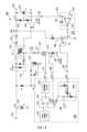
傳統的脈寬調變(PWM)返馳轉換器通常操作在電流控制模式和一恆定開關頻率。它可以設計為在連續導通模式(CCM)或在非連續導通模式(DCM)下工作。因為它具有簡單的電源電路拓撲結構,使用最少數量的功率元件,所以返馳轉換器被普遍應用於手機電池充電器等低功耗電源產品。如圖 1 所示,一典型的常規PWM 返馳轉換器 100 耦合到輸入電壓 110,並將輸入電壓 110 轉換為輸出電壓 120。返馳轉換器 100 的一次側電路主要包括輸入濾波電容器 111,功率變壓器 113,功率開關 117,電流偵測電阻 118,可選的緩衝電路 112 和 脈寬調變控制器 130。返馳轉換器 100 的二次側電路主要包括輸出二極體 121,輸出濾波電容器 125,並聯調節器 150,及光耦合器 160。A conventional pulse width modulation (PWM) flyback converter usually operates in current control mode and a constant switching frequency. It can be designed to operate in continuous conduction mode (CCM) or in discontinuous conduction mode (DCM). Because it has a simple power circuit topology and uses a minimum number of power components, flyback converters are widely used in low-power power products such as mobile phone battery chargers. As shown in FIG1 , a typical conventional
前述功率變壓器 113 的鐵氧體磁芯安裝有三個繞組:一次側繞組; 二次側繞組; 偏置電壓繞組(114)。 一次側繞組的第一端耦合到輸入電壓 110。一次側繞組的第二端則耦合到功率開關 117 的汲極。二次側繞組的第一端耦合到二次側的共同接地點 ; 二次側繞組的第二端則耦合到輸出二極體 121 的陽極。偏置電壓繞組則產生電壓予於脈寬調變控制器 130。The ferrite core of the
前述脈寬調變控制器 130 主要包括 PWM 時鐘產生器 131,SR正反器 133,閘極驅動放大器 134,電流斜坡比較器 135,和誤差電壓分壓器 140。前述並聯穩壓器 150 包括誤差放大器 151。並聯穩壓器 150 通過使用由電阻 123 和電阻 124 組成的電阻分壓器來檢測輸出電壓 120 的電位,並將該電阻分壓器的輸出電壓 126 耦合到誤差放大器 151 的反相輸入端。誤差放大器 151 的正相輸入端則耦合到一個精密參考電壓 152,例如 2.50V。電容器 153 是一可選的反饋補償元件。基本上,誤差放大器 151 的功能是根據分壓電位 126 與參考電壓 152 的時間加權電位偏差量以產生誤差電壓信號 154。例如,如果分壓電位 126 在一段時間內低於參考電壓 152,則誤差電壓信號 154 將往 5.0V方向上升。另一方面,如果分壓電位 126 在一段時間內高於參考電壓 152,則誤差電壓信號 154 將往 0.0V 方向下降。而誤差電壓信號 154 則耦合到光耦合器 160 的輸入端。光耦合器 160 的功能基本上是將二次側的誤差電壓信號 154 耦合至一次側,並複製產生幅度大致相同的一次側誤差電壓 139,並將其連結到誤差電壓分壓器 140 的輸入端。The pulse
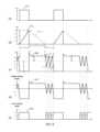
請注意,一般做法是將誤差電壓信號 154 和一次側誤差電壓 139 都設計為操作在 0.0V 至 5.0V 的電壓區間。誤差電壓分壓器 140 的功用則是將一次側誤差電壓 139 縮減成一個調節用誤差信號 136,其工作電壓區間下調到 0.0V 至大約 1.2V。另一方面,在脈寬調變控制器 130 之中,PWM 時鐘產生器 131 產生一個恆定頻率的 PWM 時鐘信號 132。於圖 1 返馳轉換器的範例中,PWM 時鐘信號 132 的恆定頻率是設定在 100 kHz,如圖 2(a) 所示。而且圖 1 返馳轉換器的範例中,輸入電壓110 是設定在 300V ; 輸出電壓120 則是設定在 20V; 全載電流設定在 3.0 A。圖 2 所示為圖 1 返馳轉換器工作在連續導通模式 (CCM) 時的關鍵信號波形。Please note that the general practice is to design the
當工作在一個穩定的 CCM 狀態下,每個 PWM 時鐘信號 132 的脈衝將觸動 SR正反器 133,其輸出信號轉正並耦合至閘極驅動放大器 134。而後者的輸出信號 137 轉成高位,而將功率開關 117 立即接通。功率開關 117 接通之後,一次側電流 115 (開始流經一次側繞組,功率開關 117,以及電流偵測電阻118,並且穩定上升。一次側電流 115 自一個初始谷值,,按照一個的斜率上升。其中,是為一次側繞組的激磁電感,則為時間變數。上升中的一次側電流 115,其波形如圖 2(c) 所示,會在電流偵測電阻 118 感應出一個電流偵測信號 138, 如圖 2(d) 所示。然後,當此電流偵測信號 138 上升到超越調節用誤差信號 136 的準位時,電流斜坡比較器 135 的輸出信號立即自低位轉成高位。此動作導致 SR 正反器 133 的重置。而 SR 正反器的重置直接導致閘極驅動放大器 134 和功率開關 117 依序關斷,如圖 2(b) 至圖 2(e) 所示。請注意,功率開關 117 導通一次側電流 115 的時間,通常被稱為「導通時間」(。When operating in a stable CCM state, each pulse of the
而在功率開關 117 關斷瞬間,一次側電流 115 立即停止在一次側導通,並且切換至二次側,形成二次側電流(122)。此電流自二次繞組經由輸出二極體 121 流向輸出濾波電容器 125 和負載電路。請注意,自功率開關 117 關斷一次側電流 115 直到下一週期之初功率開關 117 再度被接通的時間,,通常又被稱為「退磁時間」。而在期間,二次側電流 122 按照一個的斜率下降。其中,是為二次側繞組的激磁電感值,則為時間變數。請注意,在CCM 操作模式中,開關週期時間是等於與相加之和,易言之,。另請注意,在功率開關 117 關斷瞬間,其汲源極電壓會自幾近於零跳升至的高準位。而且,在 CCM 操作模式中,一次側電流 115 和二次側電流 122 不會在任何時間點同時為零。在期間,一次側電流115 自一個起始谷值上升。在時間結束時,一次側電流 115 會上升至一個的峰值。而在期間,二次側電流 122 自一個起始峰值下降。在時間結束時,二次側電流 122 會下降至一個的谷值,如圖 2(c) 所示。請注意,根據前述之公式 (1),在CCM操作模式中,返馳轉換器會承受較多的切換損耗。這是因為功率開關 117 一直在其汲源極電壓116 停留在一個最高準位,的狀況下瞬間導通。例如,假設功率開關 117 的汲源極之間寄生電容等於 100pF,為 300V,為 150V,亦即= 450V。再如前設定,等於 100kHz。將上述各值代入公式 (1),則可以算出功率開關 117 操作在 CCM 模式的切換損耗為 1.01W。When the
事實上,圖 1 返馳轉換器可以很容易被修改成為 DCM 模式下工作,這修改只需將功率變壓器的激磁電感值大幅調降,而其他電路設計參數基本上維持不變。DCM 模式與 CCM 模式主要相異處,就在於前者的開關週期時間,是等於,與三者之和。亦即在期間,一次側電流 115 自零值上升。在時間結束時,一次側電流 115 會上升至一個的峰值。而在期間,二次側電流 122 自一個起始值下降。在時間結束時,二次側電流 122 會下降至零。而在期間,二次側電流 122 和一次側電流 115 都同時停留在零的準位。所以通常又被稱為停滯時間,如圖 3(c) 所示。請注意,在期間,功率開關 117 的汲源極電壓 116,會在一個波峰值,以及一個波谷值之間往復振盪。如前述,汲源極電壓振盪的諧振週期時間,,等於。In fact, the flyback converter in Figure 1 can be easily modified to operate in DCM mode. This modification only requires a significant reduction in the magnetizing inductance of the power transformer, while other circuit design parameters remain essentially unchanged. The main difference between DCM mode and CCM mode is the switching cycle time of the former. is equal to ,and The sum of the three. exist During this period, the primary current 115 rises from zero. At the end of the time, the primary current 115 will rise to a The peak value of During this period, the secondary current 122 from a The starting value decreases. At the end of the time, the secondary current 122 will drop to zero. During this period, the secondary current 122 and the primary current 115 both stay at zero level at the same time. Often referred to as dwell time , as shown in Figure 3(c). Note that During this period, the drain-
請注意,功率開關 117 接通瞬間前的實際汲源極電壓,,會落在上述波峰值與波谷值之間,如圖 3(e) 所示。一般而言,的數值會受到數項因素影響,包括和的各別長度,輸入電壓 110,以及負載電流的大小。事實上,DCM 返馳轉換器的汲源極電壓會於期間在一波峰值與一波谷值之間進行諧振式振盪的特性,乃是準諧振式返馳轉換器,通常也稱為波谷切換返馳轉換器的原始概念形成的起源。此原始概念之所以形成,其原因也並不複雜。根據公式 (1),功率開關 117 的切換損耗是正比於的平方值。所以,如果我們可以設計出一個控制方法,確保功率開關 117 固定在其汲源極電壓 116 振盪到某一個波谷時才接通,就可以將切換損耗減少到一個最低的程度。Note that the actual drain-source voltage immediately before the
總言之, 準諧振式或者波谷切換返馳轉換器可被視為 DCM 返馳轉換器的一個子類別。圖 4 示出了現今準諧振式返馳轉換器的一個典型實施例,例如: On-Semi 的 NCP1345; 德州儀器的 UCC28600 ; 英飛淩的 ICE5QSAG。一般而言,現今準諧振式返馳轉換器不同於常規 DCM 返馳轉換器主要在於其三個獨特的子電路:(a) 零交越檢測子電路; (b) 第N波谷鎖定控制子電路; (c) 開關頻率上下限子電路,如圖 4 中準諧振式返馳轉換器 400 所用之波谷切換控制器 450 所示。 請注意如圖 1 所示,功率變壓器 113 的偏置電壓繞組(114) 原本的功能是為脈寬調變控制器 130 提供一個操作電壓 ()。然而,在準諧振式返馳轉換器 400 之中,偏置電壓繞組 114 尚可耦合到零交越檢測子電路 410,該子電路包括電阻分壓器 411 和 412 以及電壓比較器 451,如圖 4 所示。電阻分壓器 411 和 412 輸出一個波谷檢測信號 413。此波谷檢測信號 413 基本上是汲源極電壓波形的壓縮版本,但是去除其直流成分,如圖 5 所示。In summary, a quasi-resonant or valley-switching flyback converter can be considered a subcategory of a DCM flyback converter. FIG4 shows a typical implementation of a current quasi-resonant flyback converter, such as: NCP1345 from On-Semi; UCC28600 from Texas Instruments; ICE5QSAG from Infineon. Generally speaking, current quasi-resonant flyback converters differ from conventional DCM flyback converters primarily in their three unique subcircuits: (a) a zero-crossing detection subcircuit; (b) an Nth valley lock control subcircuit; and (c) a switching frequency upper and lower limit subcircuit, as shown in the
然後,波谷檢測信號 413 被耦合到電壓比較器 451 的反相輸入端,其正相輸入端連結到幾近於零的參考電位。電壓比較器 451 的輸出稱為零交越信號 452。然後零交越信號 452 耦合到第N個波谷鎖定控制子電路 453 的第一個輸入端。請注意如圖 5(d) 和圖 5(e) 所示,在每個開關週期的期間,零交越信號 452 的第一個上升緣預告即將到來的第一個波谷。零交越信號 452 的第二個上升緣預告即將到來的第二個波谷,如此類推。請再注意,開關頻率上下限子電路 455 的輸入端是耦合到 SR 正反器 133 的輸出端,以檢測準諧振式返馳轉換器 400 目前的開關頻率是否漂移到所設定的上限以上,或者漂移到所設定的下限以下。開關頻率上下限子電路 455 的輸出信號 456 耦合到第N個波谷鎖定控制子電路 453 的第二個輸入端,如圖 4 所示。Then, the
圖 6 顯示先前準諧振式返馳轉換器的一個典型波谷鎖定機制及其操作流程圖 600。以圖 4 的準諧振式返馳轉換器為例,波谷切換控制器 450 在步驟 601 開始其操作,N 的初始值被設定為 1。在完成步驟 602 的一個週期轉換器開關動作之後,波谷切換控制器 450 於步驟 603 檢查前一個開關週期的開關頻率是否超過預設上限。如果步驟 603 的結果是肯定的,則波谷切換控制器 450 繼續執行步驟 604,其中 N 的數值增加 1。然後波谷切換控制器 450 的操作返回到步驟 602。另一方面,如果步驟 603 的結果是否定的,則波谷切換控制器 450 繼續執行步驟 605,在此它檢查前一個開關週期的開關頻率是否已降至預設下限以下。如果步驟 605 的結果是肯定的,並且 N 的原先數值大於 1,則波谷切換控制器 450 繼續執行步驟 606,其中 N 的數值減去 1。然後波谷切換控制器 450 的操作返回到步驟 602。但是,如果步驟 605 的結果是否定的,那麼我們知道前一個開關週期的開關頻率是保持在上限和下限之間。因此,無需更改 N 的數值。然後波谷切換控制器 450 的操作返回到步驟 602。請注意,在實際設計中,和不必然是兩個固定值。大多數現今波谷切換控制器都會根據 N 的現值來調整和的設定值。FIG6 shows a typical valley locking mechanism of a prior art quasi-resonant flyback converter and its
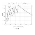
圖 7 顯示了一個典型波谷切換控制器的開關頻率對應於負載電流的特性曲線。請注意,從100% 負載到大約 50% 負載,波谷切換控制器 450 會在第一個波谷時接通功率開關 117。但是,會從 100% 負載時的 50kHz上升到 50% 負載時的約略 100kHz。從 50% 負載到大約 37% 負載,波谷切換控制器 450 會在第二個波谷時接通功率開關 117。從 37% 負載到大約 28% 負載,則在第三個波谷時動作。從 28% 負載到 19% 負載,則在第四個波谷時動作。從 19% 負載到大約 11% 負載,則在第五個波谷時動作。低於 11% 負載時,大多數現今波谷切換控制器將進入某種低頻跳越模式操作。Figure 7 shows the switching frequency of a typical valley switching controller. The characteristic curve corresponding to the load current. Note that from 100% load to about 50% load, the
圖 8 顯示了圖 4 準諧振式返馳轉換器,工作在四種不同的負載電流條件下,其汲源極電壓 116 和電流偵測信號 138 的波形。對應於 100% 負載和 50% 負載, 波谷切換控制器 450 在第一個波谷時接通功率開關 117,如圖 8(a) 及 8(b) 所示。對應於 40% 的負載,它會在第二個波谷時動作,如圖 8(c) 所示。對應於 15% 的負載,它會在第五個波谷時動作,如圖 8(d) 所示。FIG8 shows the waveforms of the drain-
然而,現有準諧振式返馳轉換器及其波谷切換控制器存在兩個缺點:(a) 第N個波谷鎖定機制相當複雜,它給控制器的設計和驗證帶來了額外的負擔。(b) 開關頻率範圍變化較大,可能導致較高的 EMI 雜訊水準。However, the existing quasi-resonant flyback converter and its valley switching controller have two disadvantages: (a) The Nth valley locking mechanism is quite complicated, which brings additional burden to the design and verification of the controller. (b) The switching frequency Larger range variations may result in higher EMI noise levels.
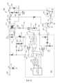
圖 9 顯示了本發明的一個優選實施例。恆定頻率準諧振式返馳轉換器 900 包括定頻波谷切換控制器 950。而定頻波谷切換控制器 950 則包括波谷檢測子電路,m 倍速時鐘產生器 953,和導通空檔 (turn-on window) 子電路 954。該 m 倍速時鐘產生器 953 以預定開關頻率的 m 倍速度發出一系列脈衝,其中 m 是等於或大於 3 的整數。在圖 9 的示範實施例中,預定開關頻率為 100kHz,而 m 設定為 4。換言之,m 倍速時鐘產生器 953 會以 400kHz 的頻率在每一個開關週期之內,發出四個脈衝,分別標記為,,及,如圖 10(a) 所示。脈衝及耦合到導通空檔子電路 954,其輸出稱為導通空檔 (turn-on window) 信號 955,如圖 10(b) 所示。在圖 9 優選實施例中,導通空檔是從脈衝開始,到脈衝結束。該導通空檔會限制 SR正反器 133 只能在脈衝之後出現的第一個波谷時才能設定(set)。但是,當處於啟動暫態或短時間過載條件下時,該準諧振式返馳轉換器可能會漂移到連續導通模式,造成在整個正常開關週期內都不會產生任何波谷。因此,在導通空檔結束時,如果仍然沒有出現任何波谷,脈衝將逕自設定 SR正反器 133。而 SR正反器 133 的復歸(reset),它是由兩個條件觸發:(a) 當 ISEN 信號 138 超越調節用誤差信號 136,或 (b) 脈衝已經到來。請注意,採用條件 (b) 是為了防止定頻準諧振式返馳轉換器 900 以大於 50% 的佔空比工作,引發穩定度問題。FIG9 shows a preferred embodiment of the present invention. The constant frequency
圖 10 顯示了圖 9 優選實施例在三個不同負載電流水準下工作的關鍵波形。圖 10(a) 顯示了每個開關週期的四倍脈衝。圖 10(b) 顯示導通空檔信號 955,其範圍自脈衝出現開始,到脈衝出現結束。圖 10(c) 顯示當定頻準諧振式返馳轉換器 900 操作在 100% 負載電流時,其116 和138 的波形。圖 10(d) 顯示當定頻準諧振式返馳轉換器 900 操作在 66% 負載電流時,其116 和138 的波形。請注意,在開關週期 1,2,和 4 中,功率開關 117 在第二個波谷處導通。但在開關週期 3 和 5 中,功率開關 117 在第一個波谷處導通。圖 10(e) 顯示當定頻準諧振式返馳轉換器 900 操作在 25% 負載電流時,其116 和138 的波形。請注意,在除了開關週期 4 以外的所有開關週期中,功率開關 117 在第五個波谷處導通。但在開關週期 4 中,功率開關 117 在第四個波谷處導通。FIG10 shows the key waveforms of the preferred embodiment of FIG9 operating at three different load current levels. FIG10(a) shows the quadruple pulse of each switching cycle. FIG10(b) shows the conduction
請注意,如圖 10(d) 和圖 10(e) 所示,本發明並無要求在穩態操作中,每個開關週期必須具有完全相同的週期時間。事實上,每個開關週期可以略長或略短於 10.0 us,這是對應於 100kHz 預定開關頻率的開關週期時間。但是,在操作一段時間後, 這些開關週期的平均值會正好等於 10.0 us。這是由於導通空檔信號 955 對 SR正反器 133 施加的一種同步效應。請另注意,定頻波谷切換控制器 950 有一個設計限制,該設計限制要求導通空檔信號 955 的寬度必須大於諧振振蕩的週期時間。如先所述,。實際上,只要定頻準諧振式返馳轉換器 900 在 DCM 模式中工作,遵守這個設計限制就可保證在每個開關週期的導通空檔信號 955 期間至少會出現一次波谷。Please note that, as shown in Figures 10(d) and 10(e), the present invention does not require that each switching cycle must have exactly the same cycle time in steady-state operation. In fact, each switching cycle can be slightly longer or shorter than 10.0 us, which is the switching cycle time corresponding to a predetermined switching frequency of 100kHz. However, after a period of operation, the average value of these switching cycles will be exactly equal to 10.0 us. This is due to a synchronization effect exerted by the on-
雖然已經通過範例和優選實施例描述了本發明,但應當理解,本發明不限於所公開的實施例。相反地,其本意乃在涵蓋對本領域技術人員顯而易見的各種修改和類似的安排。Although the present invention has been described by way of examples and preferred embodiments, it should be understood that the present invention is not limited to the disclosed embodiments. On the contrary, it is intended to cover various modifications and similar arrangements that are obvious to those skilled in the art.
100:PWM 返馳轉換器 110:輸入電壓 111:輸入濾波電容器 112:緩衝電路 (snubber circuit) 113:功率變壓器 114:功率變壓器的繞組 115:一次側電流 116:功率開關的汲源極電壓 117:功率開關 118:電流偵測電阻 120:輸出電壓 121:輸出二極體 122:二次側電流 123,124:分壓電阻 125:輸出濾波電容器 126:電阻分壓器的輸出電壓 130:脈寬調變控制器 131:PWM時鐘產生器 132:PWM時鐘信號 133:SR正反器 134:閘極驅動放大器 135:電流斜坡比較器 136:調節用誤差信號 137:閘極驅動信號 138:電流偵測信號 139:一次側誤差電壓 150:並聯調節器 (shunt regulator) 151:誤差放大器 152:參考電壓 153:可選的反饋補償元件 154:誤差電壓信號 160:光耦合器 411,412:分壓電阻 413:波谷檢測信號 450:波谷切換控制器 451:電壓比較器 452:零交越信號 453:第N個波谷鎖定控制子電路 455:開關頻率上下限子電路 456:開關頻率上下限子電路455的輸出信號 600:波谷鎖定機制操作流程圖 601:波谷鎖定機制操作流程的起始步驟 602:流程步驟,執行一個週期的轉換器開關動作 603:流程步驟,檢視開關頻率是否超過預設上限 604:流程步驟,N的數值增加1 605:流程步驟,檢視開關頻率是否低於預設下限 606:流程步驟,N的數值減去1 900:定頻準諧振式返馳轉換器 950:定頻波谷切換控制器 953:四倍速時鐘產生器 954:導通空檔子電路 955:導通空檔信號100: PWM flyback converter 110: input voltage 111: input filter capacitor 112: snubber circuit 113: power transformer 114: power transformer Winding 115: Primary current 116: Power switch drain-source voltage 117: Power switch 118: Current detection resistor 120: Output voltage 121: Output diode 122: Secondary current 123, 124: Divider resistor 125: Output filter capacitor 126: Output voltage of resistor divider 130: Pulse width modulation Controller 131: PWM clock generator 132: PWM clock signal 133: SR flip-flop 134: gate drive amplifier 135: current slope comparator 136: error signal for regulation 137: gate drive signal 138: current detection signal 139: primary side error voltage 150: shunt regulator 151: Error amplifier 152: Reference voltage 153: Optional feedback compensation element 154: Error voltage signal 160: Optocoupler 411, 412: Divider resistor 413: Valley detection signal 450: Valley switching controller 451: Voltage comparator 452: Zero crossing signal 453: Nth valley lock control Control sub-circuit 455: Switching frequency upper and lower limit sub-circuit 456: Output signal of switching frequency upper and lower limit sub-circuit 455 600: Valley lock mechanism operation flow chart 601: Starting step of valley lock mechanism operation flow 602: Flow step, execute a cycle of converter switching action 603: Flow step, check the switching frequency Whether it exceeds the preset upper limit 604: process step, the value of N increases by 1 605: process step, check the switching frequency Is it lower than the preset lower limit 606: process step, the value of N is reduced by 1 900: fixed frequency quasi-harmonic flyback converter 950: fixed frequency valley switching controller 953: four-speed clock generator 954: conduction idle sub-circuit 955: conduction idle signal
圖 1 所示為在連續導通模式或非連續導通模式下工作的傳統電流控制模式的脈寬調變返馳轉換器。Figure 1 shows a conventional current control mode PWM flyback converter operating in either continuous conduction mode or discontinuous conduction mode.
圖 2 所示為圖 1 返馳轉換器工作在連續導通模式時的關鍵信號波形。Figure 2 shows the key signal waveforms when the flyback converter in Figure 1 operates in continuous conduction mode.
圖 3 所示為圖 1 返馳轉換器工作在非連續導通模式時的關鍵信號波形。Figure 3 shows the key signal waveforms when the flyback converter in Figure 1 operates in discontinuous conduction mode.
圖 4 所示為先前技術準諧振式返馳轉換器的一個實施範例。FIG4 shows an example implementation of a prior art quasi-resonant flyback converter.
圖 5 所示為圖 4 準諧振式返馳轉換器中波谷偵測線路的關鍵信號波形。Figure 5 shows the key signal waveforms of the valley detection circuit in the quasi-resonant flyback converter of Figure 4.
圖 6 所示為圖 4 準諧振式返馳轉換器使用的一個典型波谷鎖定機制的操作流程圖。FIG6 is a flow chart showing the operation of a typical valley locking mechanism used in the quasi-resonant flyback converter of FIG4.
圖 7 所示為圖 4 準諧振式返馳轉換器的開關頻率相對於負載電流的典型特性曲線。Figure 7 shows the typical characteristic curve of the switching frequency versus load current of the quasi-resonant flyback converter in Figure 4.
圖 8 所示為圖 4 準諧振式返馳轉換器在不同負載電流狀況下的關鍵信號波形。Figure 8 shows the key signal waveforms of the quasi-resonant flyback converter in Figure 4 under different load current conditions.
圖 9 所示為根據本發明的一個優選實施例的恆定頻率準諧振式返馳轉換器的示意圖。FIG9 is a schematic diagram of a constant frequency quasi-resonant flyback converter according to a preferred embodiment of the present invention.
圖 10 所示為圖 9 恆定頻率準諧振式返馳轉換器在不同負載電流條件下的關鍵信號波形。Figure 10 shows the key signal waveforms of the constant frequency quasi-resonant flyback converter in Figure 9 under different load current conditions.
請注意,除非另有說明,術語「耦合」及其相關的動詞形式涵蓋本領域已知的各種直接和間接電路連結或其他非電路連結方式。Please note that unless otherwise stated, the term "couple" and its related verb forms cover various direct and indirect circuit connections or other non-circuit connection methods known in the art.
110:輸入電壓110: Input voltage
111:輸入濾波電容器111: Input filter capacitor
112:緩衝電路(snubber circuit)112: Snubber circuit
113:功率變壓器113: Power transformer
114:功率變壓器的n3繞組114:n3 windingof power transformer
115:一次側電流115: Primary current
116:功率開關的汲源極電壓116: Power switch drain-source voltage
117:功率開關117: Power switch
118:電流偵測電阻118: Current detection resistor
120:輸出電壓120: Output voltage
121:輸出二極體121: Output diode
122:二次側電流122: Secondary current
123,124:分壓電阻123,124: voltage divider resistor
125:輸出濾波電容器125: Output filter capacitor
133:SR正反器133:SR flip-flop
134:閘極驅動放大器134: Gate driver amplifier
135:電流斜坡比較器135: Current ramp comparator
136:調節用誤差信號136: Error signal for adjustment
137:閘極驅動信號137: Gate drive signal
138:電流偵測信號138: Current detection signal
139:一次側誤差電壓139: Primary side error voltage
150:並聯調節器(shunt regulator)150: Shunt regulator
154:誤差電壓信號154: Error voltage signal
160:光耦合器160: Optocoupler
411,412:分壓電阻411,412: voltage divider resistor
413:波谷檢測信號413: Trough detection signal
451:電壓比較器451: Voltage comparator
452:零交越信號452: Zero crossing signal
900:定頻準諧振式返馳轉換器900: Fixed frequency quasi-resonant flyback converter
950:定頻波谷切換控制器950: Constant frequency valley switching controller
953:四倍速時鐘產生器953: Quadruple speed clock generator
954:導通空檔子電路954: Turn on the neutral sub-circuit
955:導通空檔信號955: conduction neutral signal
Claims (10)
Translated fromChinesePriority Applications (1)
| Application Number | Priority Date | Filing Date | Title |
|---|---|---|---|
| TW112137660ATW202516832A (en) | 2023-10-02 | 2023-10-02 | Quasi-resonant flyback converter operating with a constant switching frequency and valley-switching controller therefor |
Applications Claiming Priority (1)
| Application Number | Priority Date | Filing Date | Title |
|---|---|---|---|
| TW112137660ATW202516832A (en) | 2023-10-02 | 2023-10-02 | Quasi-resonant flyback converter operating with a constant switching frequency and valley-switching controller therefor |
Publications (1)
| Publication Number | Publication Date |
|---|---|
| TW202516832Atrue TW202516832A (en) | 2025-04-16 |
Family
ID=96169932
Family Applications (1)
| Application Number | Title | Priority Date | Filing Date |
|---|---|---|---|
| TW112137660ATW202516832A (en) | 2023-10-02 | 2023-10-02 | Quasi-resonant flyback converter operating with a constant switching frequency and valley-switching controller therefor |
Country Status (1)
| Country | Link |
|---|---|
| TW (1) | TW202516832A (en) |
- 2023
- 2023-10-02TWTW112137660Apatent/TW202516832A/enunknown
Similar Documents
| Publication | Publication Date | Title |
|---|---|---|
| CN101019300B (en) | Isolated switching power supply unit | |
| US8339817B2 (en) | Method of operating a resonant power converter and a controller therefor | |
| US8102679B2 (en) | Utilization of a multifunctional pin to control a switched-mode power converter | |
| US5734564A (en) | High-efficiency switching power converter | |
| US9531279B2 (en) | Power supply controller with minimum-sum multi-cycle modulation | |
| CN101183830B (en) | Method and apparatus for controlling a circuit with multiple modes of operation | |
| TWI489757B (en) | Switching power converter and method for controlling the same | |
| US8149601B2 (en) | Adaptive slope compensation method for stabilizing a continuous conduction mode converter | |
| CN108933515B (en) | Flyback converter controller, flyback converter and operation method thereof | |
| EP0993105A1 (en) | Control of power transfer in a flyback converter by modulating the off-phase in function of the load | |
| US7295449B2 (en) | Simple switched-mode power supply with current and voltage limitation | |
| JP2009189170A (en) | Energy conversion device, semiconductor device used therefor, and switch control method | |
| JP2008245514A (en) | Method and apparatus for adjusting diode conduction duty cycle | |
| JP6868031B2 (en) | Power factor correction using DC / DC resonant converters and resonant converters, and corresponding control methods | |
| CN113632354B (en) | Soft Start of Resonant Converter | |
| JP2004040856A (en) | Switching power supply | |
| TW201304374A (en) | Power converters, controllers and control methods for power converters | |
| US12081109B2 (en) | Switching converter and control circuit thereof | |
| CN112189301A (en) | Totem-pole single-phase PFC converter | |
| CN112673562A (en) | Dynamic transient control in resonant converters | |
| CN112448586B (en) | LLC resonant power converter, method for controlling same and controller | |
| CN111030479B (en) | Active-clamp flyback power converter and associated control method | |
| TWI746202B (en) | A full-bridge LLC resonant converter with two-stage modulation control mechanism | |
| CN110957915B (en) | Active-clamp flyback power converter with switchable operating modes | |
| CN108365766B (en) | LLC quasi-resonant switching power supply |