TW202511532A - Pedestals for modulating film properties in atomic layer deposition (ald) substrate processing chambers and system having the same - Google Patents
Pedestals for modulating film properties in atomic layer deposition (ald) substrate processing chambers and system having the sameDownload PDFInfo
- Publication number
- TW202511532A TW202511532ATW113129674ATW113129674ATW202511532ATW 202511532 ATW202511532 ATW 202511532ATW 113129674 ATW113129674 ATW 113129674ATW 113129674 ATW113129674 ATW 113129674ATW 202511532 ATW202511532 ATW 202511532A
- Authority
- TW
- Taiwan
- Prior art keywords
- base
- substrate
- annular
- pedestal
- film layer
- Prior art date
Links
Images


Classifications
- C—CHEMISTRY; METALLURGY
- C23—COATING METALLIC MATERIAL; COATING MATERIAL WITH METALLIC MATERIAL; CHEMICAL SURFACE TREATMENT; DIFFUSION TREATMENT OF METALLIC MATERIAL; COATING BY VACUUM EVAPORATION, BY SPUTTERING, BY ION IMPLANTATION OR BY CHEMICAL VAPOUR DEPOSITION, IN GENERAL; INHIBITING CORROSION OF METALLIC MATERIAL OR INCRUSTATION IN GENERAL
- C23C—COATING METALLIC MATERIAL; COATING MATERIAL WITH METALLIC MATERIAL; SURFACE TREATMENT OF METALLIC MATERIAL BY DIFFUSION INTO THE SURFACE, BY CHEMICAL CONVERSION OR SUBSTITUTION; COATING BY VACUUM EVAPORATION, BY SPUTTERING, BY ION IMPLANTATION OR BY CHEMICAL VAPOUR DEPOSITION, IN GENERAL
- C23C16/00—Chemical coating by decomposition of gaseous compounds, without leaving reaction products of surface material in the coating, i.e. chemical vapour deposition [CVD] processes
- C23C16/44—Chemical coating by decomposition of gaseous compounds, without leaving reaction products of surface material in the coating, i.e. chemical vapour deposition [CVD] processes characterised by the method of coating
- C23C16/455—Chemical coating by decomposition of gaseous compounds, without leaving reaction products of surface material in the coating, i.e. chemical vapour deposition [CVD] processes characterised by the method of coating characterised by the method used for introducing gases into reaction chamber or for modifying gas flows in reaction chamber
- C23C16/45523—Pulsed gas flow or change of composition over time
- C23C16/45525—Atomic layer deposition [ALD]
- C23C16/45527—Atomic layer deposition [ALD] characterized by the ALD cycle, e.g. different flows or temperatures during half-reactions, unusual pulsing sequence, use of precursor mixtures or auxiliary reactants or activations
- C23C16/45536—Use of plasma, radiation or electromagnetic fields
- C—CHEMISTRY; METALLURGY
- C23—COATING METALLIC MATERIAL; COATING MATERIAL WITH METALLIC MATERIAL; CHEMICAL SURFACE TREATMENT; DIFFUSION TREATMENT OF METALLIC MATERIAL; COATING BY VACUUM EVAPORATION, BY SPUTTERING, BY ION IMPLANTATION OR BY CHEMICAL VAPOUR DEPOSITION, IN GENERAL; INHIBITING CORROSION OF METALLIC MATERIAL OR INCRUSTATION IN GENERAL
- C23C—COATING METALLIC MATERIAL; COATING MATERIAL WITH METALLIC MATERIAL; SURFACE TREATMENT OF METALLIC MATERIAL BY DIFFUSION INTO THE SURFACE, BY CHEMICAL CONVERSION OR SUBSTITUTION; COATING BY VACUUM EVAPORATION, BY SPUTTERING, BY ION IMPLANTATION OR BY CHEMICAL VAPOUR DEPOSITION, IN GENERAL
- C23C16/00—Chemical coating by decomposition of gaseous compounds, without leaving reaction products of surface material in the coating, i.e. chemical vapour deposition [CVD] processes
- C23C16/44—Chemical coating by decomposition of gaseous compounds, without leaving reaction products of surface material in the coating, i.e. chemical vapour deposition [CVD] processes characterised by the method of coating
- C23C16/455—Chemical coating by decomposition of gaseous compounds, without leaving reaction products of surface material in the coating, i.e. chemical vapour deposition [CVD] processes characterised by the method of coating characterised by the method used for introducing gases into reaction chamber or for modifying gas flows in reaction chamber
- C23C16/45523—Pulsed gas flow or change of composition over time
- C23C16/45525—Atomic layer deposition [ALD]
- C23C16/45544—Atomic layer deposition [ALD] characterized by the apparatus
- C—CHEMISTRY; METALLURGY
- C23—COATING METALLIC MATERIAL; COATING MATERIAL WITH METALLIC MATERIAL; CHEMICAL SURFACE TREATMENT; DIFFUSION TREATMENT OF METALLIC MATERIAL; COATING BY VACUUM EVAPORATION, BY SPUTTERING, BY ION IMPLANTATION OR BY CHEMICAL VAPOUR DEPOSITION, IN GENERAL; INHIBITING CORROSION OF METALLIC MATERIAL OR INCRUSTATION IN GENERAL
- C23C—COATING METALLIC MATERIAL; COATING MATERIAL WITH METALLIC MATERIAL; SURFACE TREATMENT OF METALLIC MATERIAL BY DIFFUSION INTO THE SURFACE, BY CHEMICAL CONVERSION OR SUBSTITUTION; COATING BY VACUUM EVAPORATION, BY SPUTTERING, BY ION IMPLANTATION OR BY CHEMICAL VAPOUR DEPOSITION, IN GENERAL
- C23C16/00—Chemical coating by decomposition of gaseous compounds, without leaving reaction products of surface material in the coating, i.e. chemical vapour deposition [CVD] processes
- C23C16/44—Chemical coating by decomposition of gaseous compounds, without leaving reaction products of surface material in the coating, i.e. chemical vapour deposition [CVD] processes characterised by the method of coating
- C23C16/455—Chemical coating by decomposition of gaseous compounds, without leaving reaction products of surface material in the coating, i.e. chemical vapour deposition [CVD] processes characterised by the method of coating characterised by the method used for introducing gases into reaction chamber or for modifying gas flows in reaction chamber
- C23C16/45563—Gas nozzles
- C23C16/45565—Shower nozzles
- C—CHEMISTRY; METALLURGY
- C23—COATING METALLIC MATERIAL; COATING MATERIAL WITH METALLIC MATERIAL; CHEMICAL SURFACE TREATMENT; DIFFUSION TREATMENT OF METALLIC MATERIAL; COATING BY VACUUM EVAPORATION, BY SPUTTERING, BY ION IMPLANTATION OR BY CHEMICAL VAPOUR DEPOSITION, IN GENERAL; INHIBITING CORROSION OF METALLIC MATERIAL OR INCRUSTATION IN GENERAL
- C23C—COATING METALLIC MATERIAL; COATING MATERIAL WITH METALLIC MATERIAL; SURFACE TREATMENT OF METALLIC MATERIAL BY DIFFUSION INTO THE SURFACE, BY CHEMICAL CONVERSION OR SUBSTITUTION; COATING BY VACUUM EVAPORATION, BY SPUTTERING, BY ION IMPLANTATION OR BY CHEMICAL VAPOUR DEPOSITION, IN GENERAL
- C23C16/00—Chemical coating by decomposition of gaseous compounds, without leaving reaction products of surface material in the coating, i.e. chemical vapour deposition [CVD] processes
- C23C16/44—Chemical coating by decomposition of gaseous compounds, without leaving reaction products of surface material in the coating, i.e. chemical vapour deposition [CVD] processes characterised by the method of coating
- C23C16/458—Chemical coating by decomposition of gaseous compounds, without leaving reaction products of surface material in the coating, i.e. chemical vapour deposition [CVD] processes characterised by the method of coating characterised by the method used for supporting substrates in the reaction chamber
- C23C16/4581—Chemical coating by decomposition of gaseous compounds, without leaving reaction products of surface material in the coating, i.e. chemical vapour deposition [CVD] processes characterised by the method of coating characterised by the method used for supporting substrates in the reaction chamber characterised by material of construction or surface finish of the means for supporting the substrate
- C—CHEMISTRY; METALLURGY
- C23—COATING METALLIC MATERIAL; COATING MATERIAL WITH METALLIC MATERIAL; CHEMICAL SURFACE TREATMENT; DIFFUSION TREATMENT OF METALLIC MATERIAL; COATING BY VACUUM EVAPORATION, BY SPUTTERING, BY ION IMPLANTATION OR BY CHEMICAL VAPOUR DEPOSITION, IN GENERAL; INHIBITING CORROSION OF METALLIC MATERIAL OR INCRUSTATION IN GENERAL
- C23C—COATING METALLIC MATERIAL; COATING MATERIAL WITH METALLIC MATERIAL; SURFACE TREATMENT OF METALLIC MATERIAL BY DIFFUSION INTO THE SURFACE, BY CHEMICAL CONVERSION OR SUBSTITUTION; COATING BY VACUUM EVAPORATION, BY SPUTTERING, BY ION IMPLANTATION OR BY CHEMICAL VAPOUR DEPOSITION, IN GENERAL
- C23C16/00—Chemical coating by decomposition of gaseous compounds, without leaving reaction products of surface material in the coating, i.e. chemical vapour deposition [CVD] processes
- C23C16/44—Chemical coating by decomposition of gaseous compounds, without leaving reaction products of surface material in the coating, i.e. chemical vapour deposition [CVD] processes characterised by the method of coating
- C23C16/458—Chemical coating by decomposition of gaseous compounds, without leaving reaction products of surface material in the coating, i.e. chemical vapour deposition [CVD] processes characterised by the method of coating characterised by the method used for supporting substrates in the reaction chamber
- C23C16/4582—Rigid and flat substrates, e.g. plates or discs
- C23C16/4583—Rigid and flat substrates, e.g. plates or discs the substrate being supported substantially horizontally
- C23C16/4585—Devices at or outside the perimeter of the substrate support, e.g. clamping rings, shrouds
- C—CHEMISTRY; METALLURGY
- C23—COATING METALLIC MATERIAL; COATING MATERIAL WITH METALLIC MATERIAL; CHEMICAL SURFACE TREATMENT; DIFFUSION TREATMENT OF METALLIC MATERIAL; COATING BY VACUUM EVAPORATION, BY SPUTTERING, BY ION IMPLANTATION OR BY CHEMICAL VAPOUR DEPOSITION, IN GENERAL; INHIBITING CORROSION OF METALLIC MATERIAL OR INCRUSTATION IN GENERAL
- C23C—COATING METALLIC MATERIAL; COATING MATERIAL WITH METALLIC MATERIAL; SURFACE TREATMENT OF METALLIC MATERIAL BY DIFFUSION INTO THE SURFACE, BY CHEMICAL CONVERSION OR SUBSTITUTION; COATING BY VACUUM EVAPORATION, BY SPUTTERING, BY ION IMPLANTATION OR BY CHEMICAL VAPOUR DEPOSITION, IN GENERAL
- C23C16/00—Chemical coating by decomposition of gaseous compounds, without leaving reaction products of surface material in the coating, i.e. chemical vapour deposition [CVD] processes
- C23C16/44—Chemical coating by decomposition of gaseous compounds, without leaving reaction products of surface material in the coating, i.e. chemical vapour deposition [CVD] processes characterised by the method of coating
- C23C16/50—Chemical coating by decomposition of gaseous compounds, without leaving reaction products of surface material in the coating, i.e. chemical vapour deposition [CVD] processes characterised by the method of coating using electric discharges
- C23C16/505—Chemical coating by decomposition of gaseous compounds, without leaving reaction products of surface material in the coating, i.e. chemical vapour deposition [CVD] processes characterised by the method of coating using electric discharges using radio frequency discharges
Landscapes
- Chemical & Material Sciences (AREA)
- Engineering & Computer Science (AREA)
- General Chemical & Material Sciences (AREA)
- Chemical Kinetics & Catalysis (AREA)
- Materials Engineering (AREA)
- Mechanical Engineering (AREA)
- Metallurgy (AREA)
- Organic Chemistry (AREA)
- Physics & Mathematics (AREA)
- Plasma & Fusion (AREA)
- Electromagnetism (AREA)
- Chemical Vapour Deposition (AREA)
Abstract
Description
Translated fromChinese本發明大體上關於基板處理系統,更具體而言,關於用於原子層沉積(ALD)基板處理腔室的底座。The present invention relates generally to substrate processing systems and, more particularly, to a pedestal for an atomic layer deposition (ALD) substrate processing chamber.
此處所提供之先前技術說明係為了大體上介紹本發明之背景。在此先前技術章節中所敘述之範圍內之本案列名之發明人的成果、以及在申請時不適格作為先前技術之說明書的實施態樣,皆非有意地或暗示地被承認為對抗本發明之先前技術。The prior art description provided here is for the purpose of generally introducing the background of the present invention. The achievements of the inventors named in the present case within the scope described in this prior art section and the embodiments of the specification that are not qualified as prior art at the time of application are not intended or implied to be admitted as prior art against the present invention.
基板處理系統可用以進行基板處理,例如在基板(例如半導體晶圓)上沉積或蝕刻薄膜。基板處理系統通常包含一處理腔室,其具有設置於其中的基板支座(例如底座、板件等)。基板在處理期間被設置在基板支座上。可將氣體擴散裝置(例如噴淋頭)設置於處理腔室中,以根據需要而輸送和分散處理氣體及排淨氣體。Substrate processing systems can be used to perform substrate processing, such as depositing or etching thin films on substrates (e.g., semiconductor wafers). Substrate processing systems typically include a processing chamber having a substrate support (e.g., a base, a plate, etc.) disposed therein. The substrate is disposed on the substrate support during processing. A gas diffusion device (e.g., a showerhead) can be disposed in the processing chamber to deliver and disperse process gases and exhaust gases as needed.
在某些應用中,利用電漿輔助化學氣相沉積(PECVD)或電漿輔助原子層沉積(PEALD)以沉積薄膜。在PEALD期間,進行一或多個循環以在基板上沉積薄膜。各個PEALD循環通常包含前驅物給劑、給劑排淨、RF電漿給劑、及RF排淨步驟。在沉積期間,可利用噴淋頭將處理氣體輸送至處理腔室。在RF電漿給劑期間,將RF功率供應至噴淋頭,且基板支座係接地的(或者反之亦然)。In some applications, plasma assisted chemical vapor deposition (PECVD) or plasma assisted atomic layer deposition (PEALD) is used to deposit thin films. During PEALD, one or more cycles are performed to deposit thin films on a substrate. Each PEALD cycle typically includes precursor dosing, dosing purging, RF plasma dosing, and RF purging steps. During deposition, a showerhead may be used to deliver a process gas to a processing chamber. During RF plasma dosing, RF power is supplied to the showerhead and the substrate support is grounded (or vice versa).
一種用以在處理腔室中利用原子層沉積於基板上沉積薄膜的系統,該系統包含一底座,其係設置於該處理腔室中,俾在該處理腔室中利用原子層沉積於該基板上沉積該薄膜時將該基板支撐於該底座的頂表面上。該底座中的第一環形凹部自該底座之該頂表面往下延伸且自該底座之外緣朝向該基板之外緣而徑向往內延伸。該第一環形凹部具有大於該基板之直徑的内徑。由介電材料所製成的環形環件係在該第一環形凹部中環繞該基板而設置。該底座中的第二環形凹部係位在該環形環件的下方。該第二環形凹部具有一高度且自該底座之外緣朝向該基板之外緣而徑向往內延伸。A system for depositing a thin film on a substrate using atomic layer deposition in a processing chamber, the system includes a base, which is disposed in the processing chamber so as to support the substrate on the top surface of the base when the thin film is deposited on the substrate using atomic layer deposition in the processing chamber. A first annular recess in the base extends downward from the top surface of the base and extends radially inward from the outer edge of the base toward the outer edge of the substrate. The first annular recess has an inner diameter greater than the diameter of the substrate. An annular ring made of dielectric material is disposed in the first annular recess around the substrate. A second annular recess in the base is located below the annular ring. The second annular recess has a height and extends radially inward from the outer edge of the base toward the outer edge of the substrate.
在其它特徵中,該底座係由金屬所製成。該底座之該頂表面塗布有陶瓷材料之膜層。該膜層具有中心區域及環形外側區域。該中心區域的厚度小於該環形外側區域。In other features, the base is made of metal. The top surface of the base is coated with a film layer of ceramic material. The film layer has a central region and an annular outer region. The thickness of the central region is less than that of the annular outer region.
在其它特徵中,該底座係由金屬所製成。該底座之該頂表面的環形部分塗布有陶瓷之膜層。該底座之該頂表面之位在該環形部分內的中心部分係未經塗布的。In other features, the base is made of metal. The annular portion of the top surface of the base is coated with a ceramic film. The center portion of the top surface of the base within the annular portion is uncoated.
在其它特徵中,該底座係由金屬所製成。該底座之該頂表面塗布有陶瓷材料之膜層,該膜層延伸直至該第一環形凹部的內徑。該膜層包含一凹穴,該凹穴具有小於該膜層之厚度的深度,且具有小於該基板之半徑的半徑。In other features, the base is made of metal. The top surface of the base is coated with a film of ceramic material, which extends to the inner diameter of the first annular recess. The film includes a cavity having a depth less than the thickness of the film and a radius less than the radius of the substrate.
在其它特徵中,該底座係由金屬所製成。該底座之該頂表面塗布有陶瓷材料之膜層,該膜層延伸直至該第一環形凹部的內徑。該膜層包含一凹穴,該凹穴具有等於該膜層之厚度的深度,且具有小於該基板之半徑的半徑。In other features, the base is made of metal. The top surface of the base is coated with a film of ceramic material, which extends to the inner diameter of the first annular recess. The film includes a cavity having a depth equal to the thickness of the film and having a radius less than the radius of the substrate.
在其它特徵中,一噴淋頭係設置於該處理腔室中之該底座的上方。在該處理腔室中利用原子層沉積於該基板上沉積該薄膜時,該噴淋頭接收RF功率。該底座係接地的。In other features, a showerhead is disposed above the pedestal in the processing chamber. The showerhead receives RF power when the film is deposited on the substrate using atomic layer deposition in the processing chamber. The pedestal is grounded.
在其它特徵中,一噴淋頭係設置於該處理腔室中之該底座的上方。在該處理腔室中利用原子層沉積於該基板上沉積該薄膜時,該底座接收RF功率。該噴淋頭係接地的。In other features, a showerhead is disposed above the pedestal in the processing chamber. The pedestal receives RF power when the film is deposited on the substrate using atomic layer deposition in the processing chamber. The showerhead is grounded.
在其它特徵中,一種用以在處理腔室中利用原子層沉積於基板上沉積薄膜的系統包含一底座,其係由金屬所製成且設置於該處理腔室中,俾在該處理腔室中利用原子層沉積於該基板上沉積該薄膜時將該基板支撐於該底座的頂表面上。該底座中之環形凹部自該底座之該頂表面往下延伸且自該底座之外緣朝向該基板之外緣而徑向往內延伸。該環形凹部具有大於該基板之直徑的内徑。一環形環件係由介電材料所製成,且係在該環形凹部中環繞該基板而設置。陶瓷材料之膜層塗布該底座之該頂表面的環形外側區域。In other features, a system for depositing a thin film on a substrate using atomic layer deposition in a processing chamber includes a base made of metal and disposed in the processing chamber to support the substrate on a top surface of the base while the thin film is deposited on the substrate using atomic layer deposition in the processing chamber. An annular recess in the base extends downward from the top surface of the base and radially inward from an outer edge of the base toward an outer edge of the substrate. The annular recess has an inner diameter that is greater than the diameter of the substrate. An annular ring is made of a dielectric material and is disposed around the substrate in the annular recess. A film layer of ceramic material coats an annular outer area of the top surface of the base.
在另一特徵中,該膜層之該環形外側區域延伸直至該環形凹部的內徑。In another feature, the annular outer region of the membrane layer extends to the inner diameter of the annular recess.
在其它特徵中,該膜層更包含與該環形外側區域鄰接的中心區域。該中心區域的厚度小於該環形外側區域。In other features, the film layer further includes a central region adjacent to the annular outer region. The central region has a thickness less than that of the annular outer region.
在其它特徵中,該膜層更包含與該環形外側區域鄰接的中心區域。該中心區域未塗布有該陶瓷材料。In other features, the film layer further includes a central region adjacent to the annular outer region, and the central region is not coated with the ceramic material.
在其它特徵中,該膜層更包含與該環形外側區域鄰接的中心區域。該中心區域包含一凹穴,該凹穴具有小於該膜層之厚度的深度,且具有小於該基板之半徑的半徑。In other features, the film layer further includes a central region adjacent to the annular outer region. The central region includes a cavity having a depth less than the thickness of the film layer and a radius less than the radius of the substrate.
在其它特徵中,該膜層更包含與該環形外側區域鄰接的中心區域。該中心區域包含一凹穴,該凹穴具有等於該膜層之厚度的深度,且具有小於該基板之半徑的半徑。In other features, the film layer further includes a central region adjacent to the annular outer region. The central region includes a cavity having a depth equal to the thickness of the film layer and having a radius less than the radius of the substrate.
在其它特徵中,該底座中的第二環形凹部係位在該環形環件的下方。該第二環形凹部具有一預定高度且自該底座之外緣朝向該基板之外緣而徑向往內延伸。In other features, a second annular recess in the base is located below the annular ring. The second annular recess has a predetermined height and extends radially inward from an outer edge of the base toward an outer edge of the substrate.
在其它特徵中,一噴淋頭係設置於該處理腔室中之該底座的上方。在該處理腔室中利用原子層沉積於該基板上沉積該薄膜時,該噴淋頭接收RF功率。該底座係接地的。In other features, a showerhead is disposed above the pedestal in the processing chamber. The showerhead receives RF power when the film is deposited on the substrate using atomic layer deposition in the processing chamber. The pedestal is grounded.
在其它特徵中,一噴淋頭係設置於該處理腔室中之該底座的上方。在該處理腔室中利用原子層沉積於該基板上沉積該薄膜時,該底座接收RF功率。該噴淋頭係接地的。In other features, a showerhead is disposed above the pedestal in the processing chamber. The pedestal receives RF power when the film is deposited on the substrate using atomic layer deposition in the processing chamber. The showerhead is grounded.
在其它特徵中,一種用以在處理腔室中利用原子層沉積於基板上沉積薄膜的系統包含一噴淋頭,其係設置於該處理腔室中。該噴淋頭包含內部充氣部及氣體通孔,經由該等氣體通孔而將處理氣體導入和分配於該處理腔室中。由金屬所製成的底座係設置於該處理腔室中之該噴淋頭的正下方,俾在利用原子層沉積於該基板上沉積該薄膜時將該基板支撐於該底座的頂表面上。該底座小於該噴淋頭包含該等氣體通孔的區域。陶瓷材料之膜層塗布該底座之該頂表面。該膜層包含環形外側區域、及鄰接該環形外側區域的中心區域。一凹穴係設置於該膜層的該中心區域中。該凹穴具有小於或等於該膜層之該環形外側區域之厚度的深度,且具有小於該基板之半徑的半徑。In other features, a system for depositing a thin film on a substrate using atomic layer deposition in a processing chamber includes a showerhead disposed in the processing chamber. The showerhead includes an internal plenum and gas holes through which a processing gas is introduced and distributed into the processing chamber. A base made of metal is disposed directly below the showerhead in the processing chamber to support the substrate on a top surface of the base while the thin film is deposited on the substrate using atomic layer deposition. The base is smaller than the area of the showerhead containing the gas holes. A film layer of ceramic material is coated on the top surface of the base. The film layer includes an annular outer region and a central region adjacent to the annular outer region. A cavity is disposed in the central region of the film layer. The cavity has a depth less than or equal to a thickness of the annular outer region of the film layer and has a radius less than a radius of the substrate.
在其它特徵中,在該處理腔室中利用原子層沉積於該基板上沉積該薄膜時,該噴淋頭接收RF功率。該底座係接地的。In other features, the showerhead receives RF power when depositing the film on the substrate using atomic layer deposition in the processing chamber. The pedestal is grounded.
在其它特徵中,在該處理腔室中利用原子層沉積於該基板上沉積該薄膜時,該底座接收RF功率。該噴淋頭係接地的。In other features, the pedestal receives RF power while depositing the film on the substrate using atomic layer deposition in the processing chamber. The showerhead is grounded.
本揭露內容之進一步的可應用領域將從實施方式、發明申請專利範圍及圖式中變得明顯。詳細說明及具體範例係意圖為僅供說明的目的,而非意欲限制本揭示內容的範圍。Further applicable areas of the present disclosure will become apparent from the embodiments, the scope of the invention and the drawings. The detailed description and specific examples are intended for illustrative purposes only and are not intended to limit the scope of the present disclosure.
本發明涉及用於調變薄膜蝕刻性能(包括乾式蝕刻率、下游濕式蝕刻率、薄膜密度、及折射率)的系統及方法。該等系統及方法涉及修改底座邊緣處之底座形狀因素及幾何。具體而言,減少底座的邊緣區域可提高電漿在基板上的聚焦程度,並改善沉積於基板上之薄膜的特性。此外,在底座(位於基板正下方)之頂表面上塗布陶瓷塗層可有效地調變基板性能。The present invention relates to systems and methods for modulating thin film etch properties, including dry etch rate, downstream wet etch rate, film density, and refractive index. The systems and methods involve modifying the pedestal form factor and geometry at the pedestal edge. Specifically, reducing the pedestal edge area can improve the focus of the plasma on the substrate and improve the properties of the thin film deposited on the substrate. In addition, applying a ceramic coating on the top surface of the pedestal (located directly below the substrate) can effectively modulate the substrate properties.
此外,電漿接地可緊鄰於基板,以最大程度地實現包括蝕刻率、密度、及折射率之薄膜性質。具體而言,對於經供電的噴淋頭/接地的底座之配置而言,接地可在基板的正下方,而對於接地的噴淋頭/經供電的底座之配置而言,接地可在基板的正上方。Additionally, the plasma ground can be located in close proximity to the substrate to maximize film properties including etch rate, density, and refractive index. Specifically, the ground can be directly below the substrate for a powered showerhead/grounded pedestal configuration and directly above the substrate for a grounded showerhead/powered pedestal configuration.
可藉由設計具有以下特徵的底座而實現該等系統及方法:在基板正下方之底座部分具有基板尺寸之接觸區域、且在基板尺寸之接觸區域之外的底座部分具有大型凹穴(切口)。切口使得基板平面外部的阻抗增加。替代地或附加地,可藉由設計具有以下特徵的底座而實現該等系統及方法:具有基板尺寸的底座或與噴淋頭相比而較小的底座。依據本發明之底座設計的該等及其他特徵係在下文中詳細說明。The systems and methods may be implemented by designing a base having a substrate-sized contact area in the portion of the base directly below the substrate and having a large recess (cutout) in the portion of the base outside the substrate-sized contact area. The cutout increases the impedance outside the plane of the substrate. Alternatively or additionally, the systems and methods may be implemented by designing a base having a substrate-sized base or a base that is smaller than a showerhead. These and other features of base designs according to the present invention are described in detail below.
將本發明整理如下。參照圖1而顯示和說明原子層沉積(ALD)處理腔室之範例。參照圖2A及2B而顯示和說明一底座設計,其中與基板相鄰的底座頂部自底座邊緣徑向往內凹進。參照圖3A-3C而顯示和說明一底座設計,其具有塗布於底座頂表面上的陶瓷塗層。參照圖4A-4D而顯示和說明包含凹陷與塗布特徵之組合的各種其他底座設計。圖5中顯示另一底座設計,其中底座小於噴淋頭的有效區域(亦即,包含氣體通孔的區域),其為替代圖2A及2B所示之凹陷特徵的方案。The present invention is organized as follows. An example of an atomic layer deposition (ALD) processing chamber is shown and described with reference to FIG1. A base design is shown and described with reference to FIGS. 2A and 2B, wherein the top of the base adjacent to the substrate is recessed inwardly from the base edge diameter. A base design is shown and described with reference to FIGS. 3A-3C, which has a ceramic coating applied to the top surface of the base. Various other base designs including a combination of recessed and coating features are shown and described with reference to FIGS. 4A-4D. Another base design is shown in FIG. 5, wherein the base is smaller than the effective area of the showerhead (i.e., the area including the gas through hole), which is an alternative to the recessed feature shown in FIGS. 2A and 2B.
圖1顯示包含基板支座(例如底座)104之基板處理系統100的範例。基板支座104係設置於處理腔室108內。在處理期間,基板112係設置於基板支座104上。在某些範例中,基板支座104可配置為與基板112的接觸最小化。例如,僅基板112的外緣可接觸基板支座104的上表面;基板112可設置於最小接觸面積(MCA)特徵部上;等等。雖然僅例示性地顯示和描述基板支座104的一配置方式,但本發明之教示可應用於具有不同配置的許多其他基板支座。FIG. 1 shows an example of a
氣體輸送系統120包含氣體源122-1、122-2、…、及122-N(統稱為氣體源122),其係連接至閥124-1、124-2、…、及124-N(統稱為閥124)及質量流量控制器126-1、126-2、…、及126-N(統稱為MFCs 126)。MFCs 126控制由氣體源122至歧管128之氣體流動,在歧管128之處氣體進行混合。歧管128之輸出被供應至噴淋頭140。噴淋頭140包含內部充氣部及氣體通孔。噴淋頭140經由氣體通孔將處理氣體導入和分配於處理腔室108中。The
RF產生系統130產生並輸出RF電壓至噴淋頭140或基板支座104(另一者為DC接地、AC接地、或浮動的)。僅舉例而言,RF產生系統130可包含RF電壓產生器132,其產生由匹配網路134饋送至噴淋頭140或基板支座104的RF電壓。電漿在處理氣體及RF功率被供應至噴淋頭140時產生。The
在某些範例中,在每個ALD循環期間,於給劑排淨及RF排淨步驟中,惰性氣體(例如氬(Ar)或分子氮(N2))可用作流經噴淋頭140的主要排淨氣體。此外,在所有ALD步驟中,作為輔助排淨,分子氧(O2)或分子氮(N2)可連續流過噴淋頭140的背側,俾避免在遠端區域處(如噴淋頭140的背側、及處理腔室108之壁部與頂板)產生任何非所欲之沉積。In certain examples, during each ALD cycle, during the dosing purge and RF purge steps, an inert gas, such as argon (Ar) or molecular nitrogen (N2 ), may be used as a primary purge gas through the
在一些範例中,基板支座104可包含冷卻劑通道160。冷卻流體係從流體儲存部168及泵浦170供應至冷卻劑通道160。在某些範例中,基板支座104可包含排氣式密封環帶(VSB)底座。在某些範例中,基板支座104可包含複數區帶(未圖示)。可藉由使用選用性設置於各別區域中之獨立受控的加熱器164以控制基板支座104之溫度。當有使用,加熱器164可包含電阻加熱器或薄膜加熱器。閥178及泵浦180可用以將反應物從處理腔室108中排空、及/或控制處理腔室108內的壓力。In some examples, the
控制器182控制處理氣體之流動、監視處理參數如溫度、壓力、功率等、觸發和熄滅電漿、移除反應物等。控制器182控制來自氣體輸送系統120之氣體輸送,以在處理期間每隔固定時間間隔供應處理氣體及/或排淨氣體。控制器182利用閥178及泵浦180以控制處理腔室108中之壓力及/或反應物排空。控制器182基於基板支座104中來自感測器(未圖示)的溫度反饋及/或量測冷卻劑溫度的感測器(未圖示),而控制基板支座104及基板112的溫度。The
透過以如下各種方式修改底座設計,可顯著地改善薄膜特性(特別係蝕刻率)。具體而言,下述之底座設計中的修改(單獨地和組合地)改善電漿在基板上之聚焦,其進而改善薄膜特性(例如蝕刻率)。By modifying the pedestal design in various ways as described below, thin film properties (particularly etch rate) can be significantly improved. Specifically, the modifications in the pedestal design described below (individually and in combination) improve the focusing of the plasma on the substrate, which in turn improves thin film properties (e.g., etch rate).
圖2A顯示包含底座202及聚焦環204的底座設計200。底座202係由金屬(例如鋁)所製成。聚焦環204係由介電材料所製成。底座202可包含以上圖1之說明中提及的任何底座。在某些範例中,底座202及下述之其他底座可包含複數水平堆疊的金屬(例如鋁)構件。該等構件可具有不同形狀,且可被硬焊在一起以形成底座。圖2A-5中僅顯示各個底座之頂部的一部份,以強調各種底座設計之細節。頂部具有一平坦上表面,基板208在處理期間被設置於該上表面上。Figure 2A shows a base design 200 including a
底座202包含圍繞底座202之徑向外緣的環形凹部206。環形凹部206之內徑大於基板208之直徑。聚焦環204被設置於環形凹部206上。聚焦環204亦為環形且具有高度(或厚度)d1,其大於環形凹部206之高度d2。聚焦環204之頂表面係設置於與基板208之頂表面平行的平面中,其中基板208係設置於底座202之非凹陷部分上。聚焦環204之頂表面可高於或低於基板208之頂表面。The
聚焦環204改變基板208之邊緣附近的游離率及電子密度。聚焦環204使得此區域中不樂見的電漿不連續性減少。聚焦環204物理上限制基板208在底座202上的移動。聚焦環204使得當使用某些氣體物種時可能在基板208之邊緣處出現的電漿團減少。聚焦環204在基板208之外徑處的接近性可使基板208之邊緣附近的電子密度及游離率減小。The focusing
圖2B顯示底座設計250,其中在聚焦環204緊鄰正下方的底座202之一部份徑向地往內凹入。例如,可自底座202將材料(例如,金屬如鋁)移除而形成底座202-1。底座202-1界定聚焦環204之緊鄰正下方的凹部252。凹部252的高度h大於聚焦環204及環形凹部206的高度。2B shows a base design 250 in which a portion of the base 202 directly below the
在某些實施例中,凹部252可徑向往內延伸至沿聚焦環204之外徑(或底座202的外緣)的第一垂直軸252-1與沿環形凹部206的第二垂直軸252-2之間的任一點。第一與第二垂直軸252-1、252-2垂直於基板208坐落或位處於底座202-1之非凹陷頂部上的平面。In some embodiments, the recess 252 may extend radially inward to any point between a first vertical axis 252-1 along the outer diameter of the focus ring 204 (or the outer edge of the base 202) and a second vertical axis 252-2 along the
在某些實施例中,凹部252可進一步朝向基板208下方之底座202-1之中心延伸。由於聚焦環204係由此處未圖示之其他結構所支撐,因此凹部252的範圍可廣泛地變化。再者,如參照圖5所顯示和描述,相對於創造凹部252,取而代之可完全去除凹部252並使用尺寸小於噴淋頭的底座。In some embodiments, recess 252 may extend further toward the center of base 202-1 below
底座202-1之區域254(在該處材料從底座202-1移除)提供比底座202-1之部分256(在該處材料(金屬)未從底座202-1移除)更大的電阻抗。因此,凹部252使得沉積於基板208上之薄膜的特性改變。具體而言,凹部252改善了電漿在基板208上之聚焦狀況,其進而改善薄膜特性(例如蝕刻率)。可基於欲在基板208上執行之處理、及包括噴淋頭設計等之因素而選擇第一與第二垂直軸252-1、252-2之間(或自第二垂直軸252-2進一步徑向往內)的凹部252之高度h與範圍。Regions 254 of the base 202-1 where material has been removed from the base 202-1 provide greater electrical impedance than portions 256 of the base 202-1 where material (metal) has not been removed from the base 202-1. Thus, the recess 252 causes changes in the properties of the thin film deposited on the
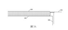
圖3A-3C顯示其他底座設計,其中諸如陶瓷材料的介電材料之塗層或膜層被設置於底座的頂表面上(亦即,底座的頂部金屬表面上)。圖3A顯示圖2A中所示之底座設計200的一部份,以強調底座202塗布有介電塗層的部分。圖3B顯示具有介電塗層的第一底座設計300。圖3C顯示具有介電塗層的第二底座設計350。3A-3C show other base designs in which a coating or film of a dielectric material, such as a ceramic material, is disposed on the top surface of the base (i.e., on the top metal surface of the base). FIG. 3A shows a portion of the base design 200 shown in FIG. 2A to emphasize the portion of the base 202 coated with the dielectric coating. FIG. 3B shows a
圖3B顯示第一底座設計300,其中介電塗層302係直接塗布於底座202之頂表面310上。基板208直接坐落於介電塗層302之上。換言之,介電塗層302與底座202之頂表面310沒有任何材料的中介層,且基板208與介電塗層302之間沒有任何材料的中介層。對於圖3B-5中所示之所有底座設計而言皆是如此。3B shows a
介電塗層302自底座202之頂表面310的中心徑向延伸至環形凹部206。介電塗層302之厚度t1小於基板208之厚度t2。一般而言,介電塗層302之厚度t1可小於或等於約一英吋的百分之一。例如,介電塗層302之厚度t1約為一英吋的千分之四至千分之八。The
在介電塗層302之靠近底座202之頂表面310的中心的部分中,形成具有直徑D及深度d的圓形凹穴312。凹穴312的深度d小於介電塗層302之厚度t1。凹穴312的直徑D小於基板208的直徑。圓形凹穴312表示環形渠溝或環形凹部,且亦可稱為圓形渠溝312或圓形凹部312。In a portion of the
介電塗層302及凹穴312使得沉積於基板208上之薄膜的特性改變。具體而言,介電塗層302及凹穴312改善電漿在基板208上之聚焦狀況,其進而改善薄膜特性(例如蝕刻率)。可基於欲在基板208上執行之處理、及包括噴淋頭設計等之因素而選擇凹穴312的直徑及深度。The
圖3C顯示第二底座設計350,其中圓形凹穴312-1向下延伸通過介電塗層302直至底座202之頂表面310。換言之,雖然凹穴312-1的直徑小於基板208的直徑(與凹穴312相似),但凹穴312-1的深度d等於介電塗層302的厚度t1(與凹穴312不同)。3C shows a
因此,在底座202的俯視圖中,在沒有基板的情況下,底座202之頂表面310係可見的。再次說明,圓形凹穴312-1表示環形渠溝或環形凹部,且亦可稱為圓形渠溝312-1或圓形凹部312-1。介電塗層302及凹穴312-1使得沉積於基板208上之薄膜的特性改變。具體而言,介電塗層302及凹穴312-1改善電漿在基板208上之聚焦狀況,其進而改善薄膜特性(例如蝕刻率)。Thus, in a top view of the
換言之,陶瓷層可被描述為具有環形外部及與環形外部鄰接的中心部分。如圖3B中所示,中心部分具有比環形外部之厚度更小的厚度。或者,如圖3C中所示,中心部分完全沒有塗層。In other words, the ceramic layer can be described as having an annular outer portion and a central portion adjacent to the annular outer portion. As shown in FIG. 3B , the central portion has a thickness that is less than the thickness of the annular outer portion. Alternatively, as shown in FIG. 3C , the central portion is completely uncoated.
圖4A-4D顯示其他底座設計,其結合圖2A-2B所示之底座設計與圖3B-3C所示之底座設計。具體而言,圖4A及4B顯示與圖3B及3C所示之介電塗層及凹穴相結合的圖2A所示底座設計200。圖4C及4D顯示與圖3B及3C所示之介電塗層及凹穴相結合的圖2B所示底座設計250。圖4A-4D中所示之組合設計進一步改善薄膜特性。僅顯示底座設計之部分以說明經結合之特徵。Figures 4A-4D show other base designs that combine the base design shown in Figures 2A-2B with the base design shown in Figures 3B-3C. Specifically, Figures 4A and 4B show the base design 200 shown in Figure 2A combined with the dielectric coating and recess shown in Figures 3B and 3C. Figures 4C and 4D show the base design 250 shown in Figure 2B combined with the dielectric coating and recess shown in Figures 3B and 3C. The combined design shown in Figures 4A-4D further improves the film properties. Only portions of the base designs are shown to illustrate the combined features.
圖4A顯示一底座設計400,其包含圖2A中所示之底座202、聚焦環204、及環形凹部206。此外,底座202包含圖3B中所示之介電塗層302及凹穴312。底座202不包含圖2B中所示之凹部252。介電塗層302及凹穴312使得沉積於基板208上之薄膜的特性改變。具體而言,介電塗層302及凹穴312改善電漿在基板208上之聚焦狀況,其進而改善薄膜特性(例如蝕刻率)。FIG4A shows a pedestal design 400 that includes the
圖4B顯示一底座設計410,其包含圖2A中所示之底座202、聚焦環204、及環形凹部206。此外,底座202包含圖3C中所示之介電塗層302及凹穴312-1。底座202不包含圖2B中所示之凹部252。介電塗層302及凹穴312-1使得沉積於基板208上之薄膜的特性改變。具體而言,介電塗層302及凹穴312-1改善電漿在基板208上之聚焦狀況,其進而改善薄膜特性(例如蝕刻率)。FIG4B shows a pedestal design 410 that includes the
圖4C顯示一底座設計420,其包含圖2B中所示之底座202-1、聚焦環204、環形凹部206、及凹部252。此外,底座202-1包含圖3B中所示之介電塗層302及凹穴312。凹部252、介電塗層302、及凹穴312使得沉積於基板208上之薄膜的特性改變。具體而言,凹部252、介電塗層302、及凹穴312改善電漿在基板208上之聚焦狀況,其進而改善薄膜特性(例如蝕刻率)。FIG4C shows a pedestal design 420 that includes the pedestal 202-1, the
圖4D顯示一底座設計430,其包含圖2B中所示之底座202-1、聚焦環204、環形凹部206、及凹部252。此外,底座202-1包含圖3C中所示之介電塗層302及凹穴312-1。凹部252、介電塗層302、及凹穴312-1使得沉積於基板208上之薄膜的特性改變。具體而言,凹部252、介電塗層302、及凹穴312-1改善電漿在基板208上之聚焦狀況,其進而改善薄膜特性(例如蝕刻率)。FIG4D shows a pedestal design 430 that includes the pedestal 202-1, the
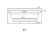
在某些實施例中,相對於在底座中提供凹部252的方式,取而代之而可使用尺寸小於噴淋頭之有效區域的底座,其使得不需要在底座中創造凹部252。此係示意性地顯示於圖5中。噴淋頭140之有效區域為內部區域A,氣體通孔位在該內部區域A之內。在尺寸上相對於噴淋頭140之有效區域A而較小的底座202-2改善電漿在基板208上之聚焦狀況,其進而改善薄膜特性(例如蝕刻率)。In some embodiments, instead of providing the recess 252 in the pedestal, a pedestal with a size smaller than the active area of the showerhead may be used, which eliminates the need to create the recess 252 in the pedestal. This is schematically shown in FIG5. The active area of the
此外,雖然未圖示,但可在底座202-2上提供介電塗層302及凹穴312/312-1,如圖3B及3C所示。較小尺寸的底座202-2與底座202-2上之介電塗層302及凹穴312/312-1之結合改善電漿在基板208上之聚焦狀況,其進而改善薄膜特性(例如蝕刻率)。In addition, although not shown, a
在上述的底座設計中,可在緊鄰基板的區域中提供接地,以最大程度地實現所期望之薄膜性質及蝕刻率。例如,當對噴淋頭供電且使底座接地時,經由位在基板之正下方的一或更多電接點而在底座中提供接地。底座中之接地接點的數量可有所變化。當對底座供電且使噴淋頭接地時,經由位在基板正上方的一或更多電接點而在噴淋頭中提供接地。噴淋頭中之接地接點的數量可有所變化。In the above-described pedestal design, grounding can be provided in an area proximate to the substrate to maximize desired film properties and etch rates. For example, when the showerhead is powered and the pedestal is grounded, grounding is provided in the pedestal via one or more electrical contacts located directly below the substrate. The number of grounding contacts in the pedestal can vary. When the pedestal is powered and the showerhead is grounded, grounding is provided in the showerhead via one or more electrical contacts located directly above the substrate. The number of grounding contacts in the showerhead can vary.
以上參照圖2A-5所描述的底座設計之任一者皆可用於圖1所示之處理腔室108中。該等底座設計增加電漿在基板上的聚焦作用,並顯著地改善薄膜特性和降低薄膜蝕刻率。Any of the pedestal designs described above with reference to Figures 2A-5 may be used in the
應注意,基板坐落於其上之陶瓷塗層302與通常用於在許多底座中支撐基板的陶瓷板有極大的不同、且因此係不可比較的。例如,在許多底座中,陶瓷板係設置於金屬底板上,其中該陶瓷板及該金屬底板形成底座。陶瓷塗層302與典型陶瓷板之間存在明顯的結構與功能差異。It should be noted that the
具體而言,陶瓷塗層302的厚度僅為大約一英吋的千分之四至千分之八,而陶瓷板的厚度為數毫米。再者,陶瓷板係利用一層黏合材料與金屬底板黏合,而陶瓷塗層302並未與金屬黏合;而是,將陶瓷塗層302噴塗於金屬的頂表面上。Specifically, the thickness of the
更重要地,典型陶瓷板包含許多元件,而陶瓷塗層302不包含任何元件。例如,在某些設計中,典型陶瓷板包含一或更多加熱器以加熱基板。相比之下,陶瓷塗層302不包含任何加熱器。在某些設計中,典型陶瓷板包含夾持電極及去夾持電極。相比之下,陶瓷塗層302不包含任何電極。再者,DC及RF偏壓可被供應至典型陶瓷板中之元件,但偏壓不被供應至陶瓷塗層302。因此,陶瓷塗層302與許多底座中所使用的陶瓷板有極大的不同、且因此係不可比較的。More importantly, a typical ceramic plate includes many components, while
以上敘述在本質上僅為說明性的,而非意圖限制本揭露內容、其應用、或用途。本揭露內容之廣泛指示可以各種形式實行。因此,雖本揭露內容包含特定例子,但由於當研究圖式、說明書、及以下申請專利範圍時,其他變化將更顯清楚,故本揭露內容之真實範疇不應如此受限。吾人應理解,在不改變本揭露內容之原理的情況下,可以不同次序(或同時)執行方法中之一或更多步驟。再者,雖實施例之各者係描述為具有某些特徵,但關於本揭露內容之任何實施例所述之任一或更多該等特徵可在任何其他實施例中實行,及/或與任何其他實施例之特徵組合(即使並未詳細敘述該組合)。換句話說,所述之實施例並非互相排斥,且一或更多實施例彼此之間的置換維持於本揭露內容之範疇內。The above description is merely illustrative in nature and is not intended to limit the present disclosure, its application, or use. The broad indications of the present disclosure may be implemented in a variety of forms. Therefore, although the present disclosure includes specific examples, the true scope of the present disclosure should not be so limited because other variations will become clear when studying the drawings, specifications, and the scope of the patent application below. It should be understood that one or more steps in the method may be performed in a different order (or simultaneously) without changing the principles of the present disclosure. Furthermore, although each of the embodiments is described as having certain features, any one or more of such features described with respect to any embodiment of the present disclosure may be implemented in any other embodiment and/or combined with features of any other embodiment (even if the combination is not described in detail). In other words, the embodiments described are not mutually exclusive, and substitutions of one or more embodiments with each other remain within the scope of the present disclosure.
元件 (例如,在模組、電路元件、半導體層等) 之間的空間及功能上之關係係使用各種用語所敘述,該等用語包含「連接」、「接合」、「耦合」、「鄰近」、「在…旁邊」、「在…之上」、「上面」、「下面」、以及「設置」。除非明確敘述為「直接」之情形下,否則當於上述揭露內容中描述第一與第二元件之間的關係時,該關係可係在第一與第二元件之間不存在其它中介元件之直接關係,但亦可係在第一與第二元件之間存在一或更多中介元件(空間上或功能上)的間接關係。如本文所使用的,詞組「A、B、及C其中至少一者」應解釋為意指使用非排除性邏輯OR之邏輯(A OR B OR C),且不應解釋為意指「A之至少一者、B之至少一者、及C之至少一者」。Spatial and functional relationships between components (e.g., in modules, circuit components, semiconductor layers, etc.) are described using various terms, including "connected," "joined," "coupled," "adjacent," "near," "on," "above," "below," and "disposed." Unless explicitly described as "directly," when describing a relationship between a first and a second component in the above disclosure, the relationship may be a direct relationship without other intervening components between the first and second components, or may be an indirect relationship with one or more intervening components (spatially or functionally) between the first and second components. As used herein, the phrase “at least one of A, B, and C” should be construed to mean a logical OR (A OR B OR C), using a non-exclusive logical OR, and should not be construed to mean “at least one of A, at least one of B, and at least one of C.”
在一些實施例中,控制器為系統的一部分,該系統可為上述例子的一部分。此系統可包含半導體處理設備,該半導體處理設備包含(複數)處理工具、(複數)腔室、(複數)處理用平台、及/或特定的處理元件(基座、氣體流動系統等)。該等系統可與電子設備整合,以在半導體晶圓或基板之處理之前、期間、以及之後,控制其運作。電子設備可被稱為「控制器」,其可控制(複數)系統的各種元件或子部件。In some embodiments, the controller is part of a system, which may be part of the above examples. The system may include semiconductor processing equipment, which includes processing tool(s), chamber(s), processing platform(s), and/or specific processing components (pedestals, gas flow systems, etc.). Such systems may be integrated with electronic devices to control their operation before, during, and after processing of semiconductor wafers or substrates. The electronic devices may be referred to as "controllers" and may control various components or subcomponents of the system(s).
取決於處理需求及/或系統類型,可將控制器程式設計成控制本文所揭露之任何處理,包含處理氣體的傳送、溫度設定(例如,加熱及/或冷卻)、壓力設定、真空設定、功率設定、RF產生器設定、RF匹配電路設定、頻率設定、流速設定、流體傳送設定、位置和操作設定、晶圓轉移(進出與特定系統連接或接合之工具及其他轉移工具、及/或負載鎖)。Depending on the processing requirements and/or system type, the controller can be programmed to control any of the processes disclosed herein, including the delivery of process gases, temperature settings (e.g., heating and/or cooling), pressure settings, vacuum settings, power settings, RF generator settings, RF matching circuit settings, frequency settings, flow rate settings, fluid delivery settings, position and operating settings, wafer transfer (in and out of tools connected or interfaced with a particular system and other transfer tools, and/or load locks).
廣泛來說,可將控制器定義為具有接收指令、發佈指令、控制運作、啟動清洗操作、啟動終點量測等之許多積體電路、邏輯、記憶體、及/或軟體的電子設備。積體電路可包含:儲存程式指令之韌體形式的晶片、數位訊號處理器(DSPs)、定義為特殊應用積體電路(ASICs)的晶片、及/或一或更多微處理器、或執行程式指令(例如,軟體)的微控制器。Broadly speaking, a controller can be defined as an electronic device with a number of integrated circuits, logic, memory, and/or software that receives commands, issues commands, controls operations, initiates cleaning operations, initiates endpoint measurements, etc. The integrated circuits may include: chips in the form of firmware that store program instructions, digital signal processors (DSPs), chips defined as application specific integrated circuits (ASICs), and/or one or more microprocessors or microcontrollers that execute program instructions (e.g., software).
程式指令可為以不同的單獨設定(或程式檔案)之形式而傳達至控制器或系統的指令,該單獨設定(或程式檔案)為實行特定處理(在半導體晶圓上,或是對半導體晶圓)定義操作參數。在一些實施例中,操作參數可係由製程工程師所定義之配方的一部分,俾在一或更多以下者(包含:覆層、材料、金屬、氧化物、矽、二氧化矽、表面、電路、及/或基板的晶粒)的製造期間實現一或更多處理步驟。Program instructions may be instructions communicated to a controller or system in the form of different individual configurations (or program files) that define operating parameters for performing a particular process (on or for a semiconductor wafer). In some embodiments, the operating parameters may be part of a recipe defined by a process engineer to perform one or more processing steps during the manufacture of one or more of the following: a die of a coating, material, metal, oxide, silicon, silicon dioxide, surface, circuit, and/or substrate.
在一些實施例中,控制器可為電腦的一部分,或耦接至電腦,該電腦係與系統整合、耦接至系統、或以網路連接至系統、或以其組合之方式連接至系統。例如,控制器可在能容許遠端存取晶圓處理之「雲端」或廠房主機電腦系統的全部或部分中。電腦可使系統能夠遠端存取,以監控製造運作的當前進度、檢查過去製造運作的歷史、由複數之製造運作而檢查趨勢或效能指標,以改變當前處理的參數、設定當前處理之後的處理步驟、或開始新的製程。In some embodiments, the controller may be part of or coupled to a computer that is integrated with the system, coupled to the system, networked to the system, or a combination thereof. For example, the controller may be in all or part of a "cloud" or factory-based host computer system that allows remote access to wafer processing. The computer may enable the system to remotely access to monitor the current progress of a manufacturing operation, review the history of past manufacturing operations, review trends or performance indicators from multiple manufacturing operations, change parameters of a current process, set processing steps after a current process, or start a new process.
在一些範例中,遠端電腦(例如,伺服器)可通過網路提供製程配方至系統,該網路可包含局域網路或網際網路。遠端電腦可包含使用者介面,其可達成參數及/或設定的接取、或對參數及/或設定進行程式化,接著將該參數及/或該設定由遠端電腦傳達至系統。在一些例子中,控制器以資料的形式接收指令,該指令為將於一或更多操作期間執行之每個處理步驟指定參數。吾人應理解,參數可特定地針對將執行之製程的類型及將控制器設定以接合或控制之工具的類型。In some examples, a remote computer (e.g., a server) may provide a process recipe to the system over a network, which may include a local area network or the Internet. The remote computer may include a user interface that may access or program parameters and/or settings that are then communicated from the remote computer to the system. In some examples, the controller receives instructions in the form of data that specify parameters for each processing step to be performed during one or more operations. It should be understood that the parameters may be specific to the type of process to be performed and the type of tool the controller is configured to engage or control.
因此,如上所述,控制器可為分散式,例如藉由包含以網路的方式連接彼此且朝向共同目的(例如,本文所敘述的製程及控制)而運作的一或更多分離的控制器。用於此目的之分散式控制器的範例將係在腔室上、與位於遠端的一或更多積體電路(例如,在作業平臺位準處、或作為遠端電腦的一部分)進行通訊的一或更多積體電路,兩者結合以控制腔室上的製程。Thus, as described above, the controller may be distributed, such as by including one or more separate controllers that are networked to each other and operate toward a common purpose (e.g., the process and control described herein). An example of a distributed controller for this purpose would be one or more integrated circuits on the chamber that communicate with one or more integrated circuits located remotely (e.g., at the work platform level or as part of a remote computer), the two combining to control the process on the chamber.
範例系統可包含但不限於以下各者:電漿蝕刻腔室或模組、沉積腔室或模組、旋轉淋洗腔室或模組、金屬電鍍腔室或模組、清洗腔室或模組、斜角緣部蝕刻腔室或模組、物理氣相沉積(PVD)腔室或模組、化學氣相沉積(CVD)腔室或模組、原子層沉積(ALD)腔室或模組、原子層蝕刻(ALE)腔室或模組、離子植入腔室或模組、軌道腔室或模組、以及可在半導體晶圓的製造及/或加工中相關聯、或使用的任何其他半導體處理系統。Example systems may include, but are not limited to, plasma etching chambers or modules, deposition chambers or modules, spin rinse chambers or modules, metal plating chambers or modules, cleaning chambers or modules, bevel edge etching chambers or modules, physical vapor deposition (PVD) chambers or modules, chemical vapor deposition (CVD) chambers or modules, atomic layer deposition (ALD) chambers or modules, atomic layer etching (ALE) chambers or modules, ion implantation chambers or modules, track chambers or modules, and any other semiconductor processing system that may be associated with or used in the manufacture and/or processing of semiconductor wafers.
如以上所提及,取決於將藉由工具執行之(複數)處理步驟,控制器可與半導體製造工廠中之一或更多的以下各者進行通訊:其他工具電路或模組、其他工具元件、群集工具、其他工具介面、鄰近之工具、相鄰之工具、遍布工廠的工具、主電腦、另一控制器、或材料運輸中所使用之工具,該材料運輸中所使用之工具將晶圓容器輸送往返於工具位置及/或裝載埠。As mentioned above, depending on the (plurality) of process steps to be performed by the tool, the controller may communicate with one or more of the following in the semiconductor manufacturing plant: other tool circuits or modules, other tool components, cluster tools, other tool interfaces, adjacent tools, neighboring tools, tools throughout the factory, a host computer, another controller, or tools used in material transport that transport wafer containers to and from tool locations and/or loading ports.
100:基板處理系統 104:基板支座 108:處理腔室 112:基板 120:氣體輸送系統 122:氣體源 122-1:氣體源 122-2:氣體源 122-N:氣體源 124:閥 124-1:閥 124-2:閥 124-N:閥 126:質量流量控制器(MFC) 126-1:質量流量控制器(MFC) 126-2:質量流量控制器(MFC) 126-N:質量流量控制器(MFC) 128:歧管 130:RF產生系統 132:RF電壓產生器 134:匹配網路 140:噴淋頭 160:冷卻劑通道 164:加熱器 168:流體儲存部 170:泵浦 178:閥 180:泵浦 182:控制器 200:底座設計 202:底座 202-1:底座 204:聚焦環 206:環形凹部 208:基板 250:底座設計 252:凹部 252-1:第一垂直軸 252-2:第二垂直軸 254:區域 256:部分 300:第一底座設計 302:介電塗層 310:頂表面 312:凹穴/圓形凹穴/圓形渠溝/圓形凹部 312-1:凹穴/圓形凹穴/圓形渠溝/圓形凹部 350:第二底座設計 400:底座設計 410:底座設計 420:底座設計 430:底座設計 A:區域 d1:高度 d2:高度 h:高度 t1:厚度 t2:厚度100: Substrate processing system104: Substrate support108: Processing chamber112: Substrate120: Gas delivery system122: Gas source122-1: Gas source122-2: Gas source122-N: Gas source124: Valve124-1: Valve124-2: Valve124-N: Valve126: Mass flow controller (MFC)126-1: Mass flow controller (MFC)126-2: Mass flow controller (MFC)126-N: Mass flow controller (MFC)128: Manifold130: RF generation system132: RF voltage generator134: Matching network140: shower head160: coolant channel164: heater168: fluid storage170: pump178: valve180: pump182: controller200: base design202: base202-1: base204: focusing ring206: annular recess208: substrate250: base design252: recess252-1: first vertical axis252-2: second vertical axis254: region256: portion300: first base design302: dielectric coating310: top surface312: Concave/circular concave/circular channel/circular recess312-1: Concave/circular concave/circular channel/circular recess350: Second base design400: Base design410: Base design420: Base design430: Base designA: Aread1: Heightd2: Heighth: Heightt1: Thicknesst2: Thickness
本揭露內容從實施方式及隨附圖式可更完全了解,其中:The present disclosure may be more fully understood from the embodiments and the accompanying drawings, in which:
圖1顯示包含原子層沉積(ALD)處理腔室之基板處理系統的範例之功能方塊圖;FIG. 1 shows a functional block diagram of an example substrate processing system including an atomic layer deposition (ALD) processing chamber;
圖2A及2B顯示具有凹陷(切口)頂部的底座,用以改善ALD處理腔室中所處理之基板的薄膜特性;2A and 2B show a pedestal with a recessed (notched) top for improving film properties of substrates processed in an ALD processing chamber;
圖3A-3C顯示具有塗布於底座頂表面上之陶瓷塗層的底座,用以改善ALD處理腔室中所處理之基板的薄膜特性;3A-3C show a pedestal having a ceramic coating applied to a top surface of the pedestal for improving film properties of a substrate processed in an ALD processing chamber;
圖4A-4D顯示包含圖2A-3C所示之凹陷與塗布特徵的組合之各種底座設計,用以進一步改善ALD處理腔室中所處理之基板的薄膜特性;以及FIGS. 4A-4D illustrate various pedestal designs including combinations of recessed and coated features as shown in FIGS. 2A-3C to further improve film properties of substrates processed in an ALD processing chamber; and
圖5顯示底座尺寸小於噴淋頭之有效區域的底座設計;FIG. 5 shows a base design where the base size is smaller than the effective area of the shower head;
在圖式中,元件符號可被再次使用以辨別相似及/或相同的元件。In the drawings, reference numerals may be reused to identify similar and/or identical elements.
202-1:底座202-1: Base
204:聚焦環204: Focus ring
206:環形凹部206: Annular concave part
208:基板208: Substrate
250:底座設計250: Base design
252:凹部252: Concave part
252-1:第一垂直軸252-1: First vertical axis
252-2:第二垂直軸252-2: Second vertical axis
254:區域254: Region
256:部分256: Partial
h:高度h: height
Claims (17)
Translated fromChineseApplications Claiming Priority (2)
| Application Number | Priority Date | Filing Date | Title |
|---|---|---|---|
| US201962802904P | 2019-02-08 | 2019-02-08 | |
| US62/802,904 | 2019-02-08 |
Publications (1)
| Publication Number | Publication Date |
|---|---|
| TW202511532Atrue TW202511532A (en) | 2025-03-16 |
Family
ID=71947378
Family Applications (2)
| Application Number | Title | Priority Date | Filing Date |
|---|---|---|---|
| TW109103310ATWI855024B (en) | 2019-02-08 | 2020-02-04 | Pedestals for modulating film properties in atomic layer deposition (ald) substrate processing chambers and system having the same |
| TW113129674ATW202511532A (en) | 2019-02-08 | 2020-02-04 | Pedestals for modulating film properties in atomic layer deposition (ald) substrate processing chambers and system having the same |
Family Applications Before (1)
| Application Number | Title | Priority Date | Filing Date |
|---|---|---|---|
| TW109103310ATWI855024B (en) | 2019-02-08 | 2020-02-04 | Pedestals for modulating film properties in atomic layer deposition (ald) substrate processing chambers and system having the same |
Country Status (5)
| Country | Link |
|---|---|
| US (2) | US12110586B2 (en) |
| KR (1) | KR20210114552A (en) |
| CN (1) | CN113423866A (en) |
| TW (2) | TWI855024B (en) |
| WO (1) | WO2020163147A1 (en) |
Family Cites Families (9)
| Publication number | Priority date | Publication date | Assignee | Title |
|---|---|---|---|---|
| US6106630A (en)* | 1997-08-07 | 2000-08-22 | Applied Materials, Inc. | Ceramic-coated heating assembly for high temperature processing chamber |
| US6475336B1 (en)* | 2000-10-06 | 2002-11-05 | Lam Research Corporation | Electrostatically clamped edge ring for plasma processing |
| US20100248397A1 (en) | 2009-03-26 | 2010-09-30 | Tokyo Electron Limited | High temperature susceptor having improved processing uniformity |
| ITCO20130041A1 (en)* | 2013-09-27 | 2015-03-28 | Lpe Spa | SUSCECTOR WITH SUPPORT ELEMENT |
| KR101568735B1 (en) | 2014-01-23 | 2015-11-12 | 주식회사 알지비하이텍 | Susceptor and substrate processing apparatus having the same |
| CN114121769B (en) | 2016-10-12 | 2025-07-22 | 朗姆研究公司 | Pad lifting mechanism for wafer positioning pedestal for semiconductor processing |
| US10622243B2 (en)* | 2016-10-28 | 2020-04-14 | Lam Research Corporation | Planar substrate edge contact with open volume equalization pathways and side containment |
| US10655224B2 (en)* | 2016-12-20 | 2020-05-19 | Lam Research Corporation | Conical wafer centering and holding device for semiconductor processing |
| US11702748B2 (en) | 2017-03-03 | 2023-07-18 | Lam Research Corporation | Wafer level uniformity control in remote plasma film deposition |
- 2020
- 2020-01-30KRKR1020217028701Apatent/KR20210114552A/ennot_activeCeased
- 2020-01-30CNCN202080013308.3Apatent/CN113423866A/enactivePending
- 2020-01-30WOPCT/US2020/015843patent/WO2020163147A1/ennot_activeCeased
- 2020-01-30USUS17/426,472patent/US12110586B2/enactiveActive
- 2020-02-04TWTW109103310Apatent/TWI855024B/enactive
- 2020-02-04TWTW113129674Apatent/TW202511532A/enunknown
- 2024
- 2024-09-25USUS18/896,365patent/US20250019825A1/enactivePending
Also Published As
| Publication number | Publication date |
|---|---|
| CN113423866A (en) | 2021-09-21 |
| US20250019825A1 (en) | 2025-01-16 |
| WO2020163147A1 (en) | 2020-08-13 |
| US12110586B2 (en) | 2024-10-08 |
| US20220162749A1 (en) | 2022-05-26 |
| TWI855024B (en) | 2024-09-11 |
| KR20210114552A (en) | 2021-09-23 |
| TW202102715A (en) | 2021-01-16 |
Similar Documents
| Publication | Publication Date | Title |
|---|---|---|
| KR102831215B1 (en) | Planar substrate edge contact with open volume equalization pathways and side containment | |
| KR20250029847A (en) | Substrate processing chamber including multiple gas injection points and dual injector | |
| JP2018014492A (en) | Electrostatic chuck having features for preventing arcing and ignition and improving process uniformity | |
| TW202000975A (en) | Substrate processing apparatus and shower head | |
| JP7743509B2 (en) | Remote plasma architecture for true radical processing | |
| JP2024056884A (en) | Preventing deposition on pedestals in semiconductor substrate processing. | |
| TWI855024B (en) | Pedestals for modulating film properties in atomic layer deposition (ald) substrate processing chambers and system having the same | |
| TWI850345B (en) | Apparatus for cleaning plasma chambers | |
| JP7685507B2 (en) | Gas distribution plate with multiple zones to optimize groove contours | |
| TW202430694A (en) | Annular pumping for chamber | |
| TW202430693A (en) | Adjustable pedestal | |
| TW202430704A (en) | Showerhead gas inlet mixer | |
| TW202421842A (en) | Showerhead for diffusion bonded, multi-zone gas dispersion |