TW202503924A - Methods of forming interconnect structures - Google Patents
Methods of forming interconnect structuresDownload PDFInfo
- Publication number
- TW202503924A TW202503924ATW113120941ATW113120941ATW202503924ATW 202503924 ATW202503924 ATW 202503924ATW 113120941 ATW113120941 ATW 113120941ATW 113120941 ATW113120941 ATW 113120941ATW 202503924 ATW202503924 ATW 202503924A
- Authority
- TW
- Taiwan
- Prior art keywords
- barrier layer
- layer
- dielectric
- treated
- gap
- Prior art date
Links
Images


Classifications
- H—ELECTRICITY
- H01—ELECTRIC ELEMENTS
- H01L—SEMICONDUCTOR DEVICES NOT COVERED BY CLASS H10
- H01L21/00—Processes or apparatus adapted for the manufacture or treatment of semiconductor or solid state devices or of parts thereof
- H01L21/70—Manufacture or treatment of devices consisting of a plurality of solid state components formed in or on a common substrate or of parts thereof; Manufacture of integrated circuit devices or of parts thereof
- H01L21/71—Manufacture of specific parts of devices defined in group H01L21/70
- H01L21/768—Applying interconnections to be used for carrying current between separate components within a device comprising conductors and dielectrics
- H01L21/76801—Applying interconnections to be used for carrying current between separate components within a device comprising conductors and dielectrics characterised by the formation and the after-treatment of the dielectrics, e.g. smoothing
- H01L21/76802—Applying interconnections to be used for carrying current between separate components within a device comprising conductors and dielectrics characterised by the formation and the after-treatment of the dielectrics, e.g. smoothing by forming openings in dielectrics
- H01L21/76814—Applying interconnections to be used for carrying current between separate components within a device comprising conductors and dielectrics characterised by the formation and the after-treatment of the dielectrics, e.g. smoothing by forming openings in dielectrics post-treatment or after-treatment, e.g. cleaning or removal of oxides on underlying conductors
- H—ELECTRICITY
- H01—ELECTRIC ELEMENTS
- H01L—SEMICONDUCTOR DEVICES NOT COVERED BY CLASS H10
- H01L21/00—Processes or apparatus adapted for the manufacture or treatment of semiconductor or solid state devices or of parts thereof
- H01L21/70—Manufacture or treatment of devices consisting of a plurality of solid state components formed in or on a common substrate or of parts thereof; Manufacture of integrated circuit devices or of parts thereof
- H01L21/71—Manufacture of specific parts of devices defined in group H01L21/70
- H01L21/768—Applying interconnections to be used for carrying current between separate components within a device comprising conductors and dielectrics
- H01L21/76801—Applying interconnections to be used for carrying current between separate components within a device comprising conductors and dielectrics characterised by the formation and the after-treatment of the dielectrics, e.g. smoothing
- H01L21/76822—Modification of the material of dielectric layers, e.g. grading, after-treatment to improve the stability of the layers, to increase their density etc.
- H01L21/76826—Modification of the material of dielectric layers, e.g. grading, after-treatment to improve the stability of the layers, to increase their density etc. by contacting the layer with gases, liquids or plasmas
- H—ELECTRICITY
- H01—ELECTRIC ELEMENTS
- H01L—SEMICONDUCTOR DEVICES NOT COVERED BY CLASS H10
- H01L21/00—Processes or apparatus adapted for the manufacture or treatment of semiconductor or solid state devices or of parts thereof
- H01L21/70—Manufacture or treatment of devices consisting of a plurality of solid state components formed in or on a common substrate or of parts thereof; Manufacture of integrated circuit devices or of parts thereof
- H01L21/71—Manufacture of specific parts of devices defined in group H01L21/70
- H01L21/768—Applying interconnections to be used for carrying current between separate components within a device comprising conductors and dielectrics
- H01L21/76801—Applying interconnections to be used for carrying current between separate components within a device comprising conductors and dielectrics characterised by the formation and the after-treatment of the dielectrics, e.g. smoothing
- H01L21/76829—Applying interconnections to be used for carrying current between separate components within a device comprising conductors and dielectrics characterised by the formation and the after-treatment of the dielectrics, e.g. smoothing characterised by the formation of thin functional dielectric layers, e.g. dielectric etch-stop, barrier, capping or liner layers
- H01L21/76834—Applying interconnections to be used for carrying current between separate components within a device comprising conductors and dielectrics characterised by the formation and the after-treatment of the dielectrics, e.g. smoothing characterised by the formation of thin functional dielectric layers, e.g. dielectric etch-stop, barrier, capping or liner layers formation of thin insulating films on the sidewalls or on top of conductors
- H—ELECTRICITY
- H01—ELECTRIC ELEMENTS
- H01L—SEMICONDUCTOR DEVICES NOT COVERED BY CLASS H10
- H01L21/00—Processes or apparatus adapted for the manufacture or treatment of semiconductor or solid state devices or of parts thereof
- H01L21/70—Manufacture or treatment of devices consisting of a plurality of solid state components formed in or on a common substrate or of parts thereof; Manufacture of integrated circuit devices or of parts thereof
- H01L21/71—Manufacture of specific parts of devices defined in group H01L21/70
- H01L21/768—Applying interconnections to be used for carrying current between separate components within a device comprising conductors and dielectrics
- H01L21/76838—Applying interconnections to be used for carrying current between separate components within a device comprising conductors and dielectrics characterised by the formation and the after-treatment of the conductors
- H01L21/76841—Barrier, adhesion or liner layers
- H01L21/76843—Barrier, adhesion or liner layers formed in openings in a dielectric
- H01L21/76846—Layer combinations
- H—ELECTRICITY
- H01—ELECTRIC ELEMENTS
- H01L—SEMICONDUCTOR DEVICES NOT COVERED BY CLASS H10
- H01L21/00—Processes or apparatus adapted for the manufacture or treatment of semiconductor or solid state devices or of parts thereof
- H01L21/70—Manufacture or treatment of devices consisting of a plurality of solid state components formed in or on a common substrate or of parts thereof; Manufacture of integrated circuit devices or of parts thereof
- H01L21/71—Manufacture of specific parts of devices defined in group H01L21/70
- H01L21/768—Applying interconnections to be used for carrying current between separate components within a device comprising conductors and dielectrics
- H01L21/76838—Applying interconnections to be used for carrying current between separate components within a device comprising conductors and dielectrics characterised by the formation and the after-treatment of the conductors
- H01L21/76841—Barrier, adhesion or liner layers
- H01L21/76853—Barrier, adhesion or liner layers characterized by particular after-treatment steps
- H01L21/76861—Post-treatment or after-treatment not introducing additional chemical elements into the layer
- H01L21/76862—Bombardment with particles, e.g. treatment in noble gas plasmas; UV irradiation
- H—ELECTRICITY
- H01—ELECTRIC ELEMENTS
- H01L—SEMICONDUCTOR DEVICES NOT COVERED BY CLASS H10
- H01L21/00—Processes or apparatus adapted for the manufacture or treatment of semiconductor or solid state devices or of parts thereof
- H01L21/70—Manufacture or treatment of devices consisting of a plurality of solid state components formed in or on a common substrate or of parts thereof; Manufacture of integrated circuit devices or of parts thereof
- H01L21/71—Manufacture of specific parts of devices defined in group H01L21/70
- H01L21/768—Applying interconnections to be used for carrying current between separate components within a device comprising conductors and dielectrics
- H01L21/76838—Applying interconnections to be used for carrying current between separate components within a device comprising conductors and dielectrics characterised by the formation and the after-treatment of the conductors
- H01L21/76841—Barrier, adhesion or liner layers
- H01L21/76853—Barrier, adhesion or liner layers characterized by particular after-treatment steps
- H01L21/76861—Post-treatment or after-treatment not introducing additional chemical elements into the layer
- H01L21/76864—Thermal treatment
- H—ELECTRICITY
- H01—ELECTRIC ELEMENTS
- H01L—SEMICONDUCTOR DEVICES NOT COVERED BY CLASS H10
- H01L21/00—Processes or apparatus adapted for the manufacture or treatment of semiconductor or solid state devices or of parts thereof
- H01L21/70—Manufacture or treatment of devices consisting of a plurality of solid state components formed in or on a common substrate or of parts thereof; Manufacture of integrated circuit devices or of parts thereof
- H01L21/71—Manufacture of specific parts of devices defined in group H01L21/70
- H01L21/768—Applying interconnections to be used for carrying current between separate components within a device comprising conductors and dielectrics
- H01L21/76838—Applying interconnections to be used for carrying current between separate components within a device comprising conductors and dielectrics characterised by the formation and the after-treatment of the conductors
- H01L21/76877—Filling of holes, grooves or trenches, e.g. vias, with conductive material
- H01L21/76879—Filling of holes, grooves or trenches, e.g. vias, with conductive material by selective deposition of conductive material in the vias, e.g. selective C.V.D. on semiconductor material, plating
- H—ELECTRICITY
- H01—ELECTRIC ELEMENTS
- H01L—SEMICONDUCTOR DEVICES NOT COVERED BY CLASS H10
- H01L21/00—Processes or apparatus adapted for the manufacture or treatment of semiconductor or solid state devices or of parts thereof
- H01L21/70—Manufacture or treatment of devices consisting of a plurality of solid state components formed in or on a common substrate or of parts thereof; Manufacture of integrated circuit devices or of parts thereof
- H01L21/71—Manufacture of specific parts of devices defined in group H01L21/70
- H01L21/768—Applying interconnections to be used for carrying current between separate components within a device comprising conductors and dielectrics
- H01L21/76838—Applying interconnections to be used for carrying current between separate components within a device comprising conductors and dielectrics characterised by the formation and the after-treatment of the conductors
- H01L21/76877—Filling of holes, grooves or trenches, e.g. vias, with conductive material
- H01L21/76883—Post-treatment or after-treatment of the conductive material
- H—ELECTRICITY
- H01—ELECTRIC ELEMENTS
- H01L—SEMICONDUCTOR DEVICES NOT COVERED BY CLASS H10
- H01L23/00—Details of semiconductor or other solid state devices
- H01L23/52—Arrangements for conducting electric current within the device in operation from one component to another, i.e. interconnections, e.g. wires, lead frames
- H01L23/522—Arrangements for conducting electric current within the device in operation from one component to another, i.e. interconnections, e.g. wires, lead frames including external interconnections consisting of a multilayer structure of conductive and insulating layers inseparably formed on the semiconductor body
- H01L23/532—Arrangements for conducting electric current within the device in operation from one component to another, i.e. interconnections, e.g. wires, lead frames including external interconnections consisting of a multilayer structure of conductive and insulating layers inseparably formed on the semiconductor body characterised by the materials
- H01L23/53204—Conductive materials
- H01L23/53209—Conductive materials based on metals, e.g. alloys, metal silicides
- H01L23/53228—Conductive materials based on metals, e.g. alloys, metal silicides the principal metal being copper
- H01L23/53238—Additional layers associated with copper layers, e.g. adhesion, barrier, cladding layers
Landscapes
- Engineering & Computer Science (AREA)
- Physics & Mathematics (AREA)
- Condensed Matter Physics & Semiconductors (AREA)
- General Physics & Mathematics (AREA)
- Computer Hardware Design (AREA)
- Microelectronics & Electronic Packaging (AREA)
- Power Engineering (AREA)
- Manufacturing & Machinery (AREA)
- Plasma & Fusion (AREA)
- Chemical Vapour Deposition (AREA)
- Formation Of Insulating Films (AREA)
Abstract
Description
Translated fromChinese本揭示案的實施例大體上係關於在微電子元件中形成互連結構的方法。更特定言之,本揭示案的實施例係關於在微電子元件中形成互連結構期間改善阻障層及襯墊性質的方法。Embodiments of the present disclosure generally relate to methods for forming interconnect structures in microelectronic devices. More particularly, embodiments of the present disclosure relate to methods for improving barrier and pad properties during the formation of interconnect structures in microelectronic devices.
諸如半導體或積體電路的微電子元件可包括數百萬個電子電路元件,諸如電晶體、電容器等。為了進一步增加在積體電路上發現的元件的密度,甚至需要更小的特徵大小。為了實現這些更小的特徵大小,必須減小導線、通孔及互連、閘極等的大小。提高電路密度及品質需要多級互連結構的可靠形成。製造技術的進步使得銅能夠用於導線、互連、通孔及其他結構。然而,隨著特徵大小的減小及銅用於互連的增加,互連結構中的電遷移成為需要克服的更大障礙。這種電遷移可能不利地影響積體電路的各種部件的電性質。Microelectronic components such as semiconductors or integrated circuits may include millions of electronic circuit components such as transistors, capacitors, etc. In order to further increase the density of components found on integrated circuits, even smaller feature sizes are required. In order to achieve these smaller feature sizes, the size of wires, vias and interconnects, gates, etc. must be reduced. Improving circuit density and quality requires the reliable formation of multi-level interconnect structures. Advances in manufacturing technology have enabled copper to be used for wires, interconnects, vias, and other structures. However, with the reduction in feature size and the increase in the use of copper for interconnects, electrical migration in the interconnect structures has become a greater obstacle to overcome. This electrical migration may adversely affect the electrical properties of various components of the integrated circuit.
當將電晶體及互連縮放到3 nm節點及縮放更多時,多個挑戰阻礙了功率及效能改進。互連包括在相同元件層內傳輸電流的金屬線及在多層之間傳輸電流的金屬通孔。間距減小會使兩者的寬度變窄且增加電阻,且亦會增加電路上的電壓降,從而限制電路速度且增加功率消耗。As transistors and interconnects are scaled to the 3 nm node and beyond, multiple challenges hinder power and performance improvements. Interconnects include metal wires that carry current within the same device layer and metal vias that carry current between multiple layers. Shrinking the spacing narrows the width of both and increases resistance, and also increases voltage drops across the circuit, limiting circuit speed and increasing power consumption.
雖然電晶體效能隨著縮放而提高,但對於互連金屬來說就不一樣了。隨著尺寸的縮小,互連通孔電阻可增加10倍。互連通孔電阻的增加可能導致阻容(resistive-capacitive, RC)延遲,此等延遲降低了效能且增加了功率消耗。習知的銅互連結構包括沉積在間隙的側壁上的阻障層及/或金屬襯墊,此等側壁提供由介電材料製成的側壁上的通孔,這提供了良好的黏著性且防止銅擴散到介電層中。由於高電阻率,阻障層通常可為通孔電阻的最大貢獻者。While transistor performance improves with scaling, the same cannot be said for interconnect metals. Interconnect via resistance can increase by a factor of 10 as dimensions shrink. Increased interconnect via resistance can result in resistive-capacitive (RC) delays that reduce performance and increase power consumption. Known copper interconnect structures include barrier layers and/or metal pads deposited on the sidewalls of the gap that provide through-holes on the sidewalls made of dielectric material, which provides good adhesion and prevents copper from diffusing into the dielectric layer. The barrier layer can often be the largest contributor to via resistance due to the high resistivity.
當前的製程包括將阻障層暴露於電漿處理,這降低了阻障層的電阻率且改善了阻障層及襯墊性質。然而,目前的電漿處理損壞互連中的其他層,諸如低k介電層,且增加電容,這降低了整體元件效能。Current processes involve exposing the barrier layer to a plasma treatment, which reduces the barrier layer's resistivity and improves barrier and pad properties. However, current plasma treatments damage other layers in the interconnect, such as low-k dielectric layers, and increase capacitance, which reduces overall device performance.
因此,需要在不增加電容及/或損壞互連結構中的其他層的情況下改善阻障層及襯墊性質的方法。Therefore, there is a need for methods to improve barrier and pad properties without increasing capacitance and/or damaging other layers in the interconnect structure.
本揭示案的一或多個實施例係關於一種形成微電子元件的方法。此方法包含在半導體基板上共形地沉積阻障層;及用微波輻射處理此阻障層以形成經處理阻障層。One or more embodiments of the present disclosure relate to a method of forming a microelectronic device. The method includes conformally depositing a barrier layer on a semiconductor substrate; and treating the barrier layer with microwave radiation to form a treated barrier layer.
本揭示案的附加實施例係關於一種形成微電子元件的方法。此方法包含在半導體基板上的介電層上共形地沉積阻障層,此介電層包含界定間隙的至少一個特徵,此間隙包括包含低k介電材料的側壁及底部,此阻障層沿著此等側壁及此底部形成在此間隙中;及用微波輻射處理此阻障層以形成經處理阻障層。Additional embodiments of the present disclosure relate to a method of forming a microelectronic device. The method includes conformally depositing a barrier layer on a dielectric layer on a semiconductor substrate, the dielectric layer including at least one feature defining a gap, the gap including sidewalls and a bottom including a low-k dielectric material, the barrier layer being formed in the gap along the sidewalls and the bottom, and treating the barrier layer with microwave radiation to form a treated barrier layer.
本揭示案的另外實施例係關於一種形成微電子元件的方法。此方法包含在半導體基板上的介電層上選擇性地沉積自組裝單層(self-assembled monolayer, SAM),此介電層包含界定間隙的至少一個特徵,此間隙包括包含低k介電材料的側壁及底部,此SAM選擇性地沉積在此間隙的此底部上;沿著此等側壁在此間隙中共形地沉積阻障層;用微波輻射處理此阻障層以形成經處理阻障層;在此經處理阻障層上沉積金屬襯墊;在將此金屬襯墊沉積在此經處理阻障層上之後移除此SAM;及在此金屬襯墊上進行間隙填充製程。Another embodiment of the present disclosure is directed to a method of forming a microelectronic device. The method includes selectively depositing a self-assembled monolayer (SAM) on a dielectric layer on a semiconductor substrate, the dielectric layer including at least one feature defining a gap, the gap including sidewalls and a bottom including a low-k dielectric material, the SAM selectively deposited on the bottom of the gap; conformally depositing a barrier layer in the gap along the sidewalls; treating the barrier layer with microwave radiation to form a treated barrier layer; depositing a metal pad on the treated barrier layer; removing the SAM after depositing the metal pad on the treated barrier layer; and performing a gapfill process on the metal pad.
在描述本揭示案的幾個例示性實施例之前,應當理解,本揭示案不限於以下描述中闡述的構造或製程步驟的細節。本揭示案能夠具有其他實施例且能夠以各種方式實踐或執行。Before describing several exemplary embodiments of the present disclosure, it should be understood that the present disclosure is not limited to the details of construction or process steps set forth in the following description. The present disclosure is capable of other embodiments and can be practiced or carried out in various ways.
本文所使用的術語「約」意謂近似或接近,且在此數值或範圍的上下文中,意謂數值的±15%或更小的變化。例如,相差±14%、±10%、±5%、±2%、±1%、±0.5%,或±0.1%的值將滿足「約」的定義。As used herein, the term "about" means approximately or close to, and in the context of this numerical value or range, means a variation of ±15% or less of the numerical value. For example, values that differ by ±14%, ±10%, ±5%, ±2%, ±1%, ±0.5%, or ±0.1% would meet the definition of "about".
如本說明書及所附發明申請專利範圍中所用,術語「基板」或「晶圓」係指製程作用其上的表面或表面的部分。熟習此項技術者還將理解,除非上下文明確指示,否則對基板的提及可僅代表基板的一部分。此外,提及在基板上沉積可意謂裸基板及其上沉積或形成有一或多個膜或特徵的基板。As used in this specification and the appended claims, the term "substrate" or "wafer" refers to a surface or portion of a surface on which a process acts. Those skilled in the art will also understand that unless the context clearly indicates otherwise, reference to a substrate may refer to only a portion of a substrate. In addition, reference to deposition on a substrate may refer to both a bare substrate and a substrate on which one or more films or features are deposited or formed.
本文所使用的「基板表面」係指在製造製程期間進行膜處理的任何基板或基板上形成的材料表面。例如,可在其上執行處理的基板表面包括諸如矽、氧化矽、應變矽、絕緣體上矽(silicon on insulator, SOI)、碳摻雜氧化矽、非晶矽、摻雜矽、鍺、砷化鎵的材料,以及諸如金屬、金屬氮化物、金屬合金及其他導電材料的任何其他材料,這取決於應用。基板包括但不限於半導體晶圓。基板可暴露於預處理製程,以拋光、蝕刻、還原、氧化、羥基化、退火及/或烘烤基板表面。除了直接在基板本身的表面上進行膜處理之外,在本揭示案中,亦可在形成於基板上的下層上進行揭示的任何膜處理步驟,如下文更詳細地揭示的,且術語「基板表面」旨在包括如上下文所指示的這種下層。因此,例如,在膜/層或部分膜/層已沉積到基板表面上的情況下,新沉積的膜/層的暴露表面變成基板表面。As used herein, "substrate surface" refers to any substrate or surface of a material formed on a substrate that is subjected to film processing during a manufacturing process. For example, substrate surfaces on which processing may be performed include materials such as silicon, silicon oxide, strained silicon, silicon on insulator (SOI), carbon doped silicon oxide, amorphous silicon, doped silicon, germanium, gallium arsenide, and any other materials such as metals, metal nitrides, metal alloys, and other conductive materials, depending on the application. Substrates include, but are not limited to, semiconductor wafers. The substrate may be exposed to pre-treatment processes to polish, etch, reduce, oxidize, hydroxylate, anneal, and/or bake the substrate surface. In addition to performing film treatments directly on the surface of the substrate itself, any film treatment steps disclosed in the present disclosure may also be performed on an underlying layer formed on the substrate, as disclosed in more detail below, and the term "substrate surface" is intended to include such underlying layers as the context indicates. Thus, for example, where a film/layer or portion of a film/layer has been deposited onto a substrate surface, the exposed surface of the newly deposited film/layer becomes the substrate surface.
基板表面可具有形成在其中的一或多個特徵、形成在其上的一或多個層及其組合。特徵的形狀可為任何適合的形狀,包括但不限於溝槽、孔及通孔(圓形或多邊形)。如在這方面所使用的,術語「特徵」係指任何有意的表面不規則性。特徵的適合實例包括但不限於延伸到基板中的具有頂部、兩個側壁及底部的溝槽,以及延伸到基板中至底部的具有一或多個側壁的通孔。The substrate surface may have one or more features formed therein, one or more layers formed thereon, and combinations thereof. The shape of the features may be any suitable shape, including but not limited to trenches, holes, and through-holes (circular or polygonal). As used in this regard, the term "feature" refers to any intentional surface irregularity. Suitable examples of features include but are not limited to trenches extending into the substrate having a top, two sidewalls, and a bottom, and through-holes extending into the substrate to the bottom having one or more sidewalls.
術語「在……上」表示元件之間存在直接接觸。術語「直接在……上」表示元件之間存在直接接觸,沒有中間元件。The term "on" indicates that there is direct contact between components. The term "directly on" indicates that there is direct contact between components, without intervening components.
如本說明書及所附發明申請專利範圍中所用,術語「前驅物」、「反應物」、「反應氣體」及類似術語可互換使用,以代表可與基板表面反應的任何氣體物種。As used in this specification and the appended claims, the terms "precursor", "reactant", "reactant gas" and similar terms are used interchangeably to represent any gaseous species that can react with the substrate surface.
本揭示案的一些實施例提供了用於改善互連的效能的方法。互連包含在相同元件層內傳輸電流的金屬線及在層之間傳輸電流的金屬通孔。這些線及通孔在元件內形成的間隙中用諸如銅或鈷的導電金屬形成。在一或多個實施例中,介電層包含界定間隙的至少一個特徵,此間隙包括側壁及底部。在一或多個實施例中,間隙包含金屬線及金屬通孔。在一或多個實施例中,金屬線具有側壁及底部。在一或多個實施例中,金屬通孔具有側壁及底部。如本說明書及所附發明申請專利範圍中所使用的,除非另有說明,否則提及「間隙的底部」旨在表示最靠近基板的金屬通孔的底部。Some embodiments of the present disclosure provide methods for improving the performance of interconnects. The interconnects include metal lines that carry current within the same component layer and metal vias that carry current between layers. These lines and vias are formed with a conductive metal such as copper or cobalt in a gap formed within the component. In one or more embodiments, the dielectric layer includes at least one feature that defines the gap, and the gap includes sidewalls and a bottom. In one or more embodiments, the gap includes metal lines and metal vias. In one or more embodiments, the metal lines have sidewalls and a bottom. In one or more embodiments, the metal vias have sidewalls and a bottom. As used in this specification and the attached invention application scope, unless otherwise specified, reference to "the bottom of the gap" is intended to mean the bottom of the metal via closest to the substrate.
本揭示案的實施例有利地提供了用於改善互連結構(諸如銅互連結構)的阻障層及襯墊性質的方法。本揭示案的一或多個實施例有利地提供了用於在不使用電漿的情況下改善互連結構的阻障層及襯墊性質的方法。具體實施例有利地提供了用於改善阻障層及襯墊性質的方法,此等阻障層及襯墊性質不會損壞結構中的其他層,諸如低k介電層。Embodiments of the present disclosure advantageously provide methods for improving barrier and pad properties of interconnect structures, such as copper interconnect structures. One or more embodiments of the present disclosure advantageously provide methods for improving barrier and pad properties of interconnect structures without using plasma. Specific embodiments advantageously provide methods for improving barrier and pad properties that do not damage other layers in the structure, such as low-k dielectric layers.
本揭示案的實施例提供了一種用於處理工具的組件。在一或多個實施例中,組件包含源陣列及外殼。在一實施例中,源陣列包含介電板、延伸到介電板中的複數個腔以及在腔中的每一者中的複數個介電共振器。在一或多個實施例中,介電共振器的寬度小於腔的寬度,使得間隙將介電共振器的側壁與腔的側壁分開。在一或多個實施例中,外殼包含導電主體及穿過導電主體的開口。介電共振器可處於開口內。在一或多個實施例中,外殼還包含在間隙中的導電環,此導電環將介電共振器的側壁與腔的側壁分開。Embodiments of the present disclosure provide an assembly for a processing tool. In one or more embodiments, the assembly includes a source array and a housing. In one embodiment, the source array includes a dielectric plate, a plurality of cavities extending into the dielectric plate, and a plurality of dielectric resonators in each of the cavities. In one or more embodiments, the width of the dielectric resonator is less than the width of the cavity, so that a gap separates the sidewalls of the dielectric resonator from the sidewalls of the cavity. In one or more embodiments, the housing includes a conductive body and an opening through the conductive body. The dielectric resonator may be within the opening. In one or more embodiments, the housing further includes a conductive ring in the gap, which separates the sidewalls of the dielectric resonator from the sidewalls of the cavity.
本揭示案的實施例提供了在微電子元件的製造中形成互連結構的方法。在一或多個實施例中,本文所述的微電子元件包含互連到至少一個底部互連結構的至少一個頂部互連結構。本揭示案的實施例提供了微電子元件及改進互連的效能(例如,降低通孔電阻)的製造微電子元件的方法。Embodiments of the present disclosure provide methods for forming interconnect structures in the manufacture of microelectronic devices. In one or more embodiments, the microelectronic devices described herein include at least one top interconnect structure interconnected to at least one bottom interconnect structure. Embodiments of the present disclosure provide microelectronic devices and methods for manufacturing microelectronic devices that improve the performance of interconnects (e.g., reduce through-hole resistance).
本揭示案的實施例利用微波製程。有利地,微波的能量可經調諧到足夠低,使得其實質上不會損壞介電材料(例如,沒有電漿及/或低溫)。此外,所揭示的方法因僅影響結構中的阻障層及金屬襯墊而不影響其他層(諸如介電層),從而係自限制的。Embodiments of the present disclosure utilize microwave processing. Advantageously, the energy of the microwaves can be tuned to be low enough so that they do not substantially damage the dielectric material (e.g., no plasma and/or low temperature). In addition, the disclosed method is self-limiting because it only affects the barrier layer and metal pad in the structure and does not affect other layers (such as dielectric layers).
藉助於附圖描述本揭示案的實施例,此等附圖示出了根據本揭示案的一或多個實施例的製程、基板及裝置。所示的方法及所得基板僅為所揭示製程的說明,且熟習此項技術者將認識到所揭示製程不限於所示應用。Embodiments of the present disclosure are described with the aid of the accompanying drawings, which illustrate processes, substrates, and devices according to one or more embodiments of the present disclosure. The methods and resulting substrates shown are merely illustrative of the disclosed processes, and those skilled in the art will recognize that the disclosed processes are not limited to the applications shown.
在以下描述中,闡述了許多具體細節以提供對本揭示案的實施例的透徹理解。對於熟習此項技術者顯而易見的為,可在沒有這些具體細節的情況下實踐實施例。在其他情況下,沒有詳細描述公知的態樣,以免不必要地混淆實施例。此外,應當理解,隨附圖式中所示的各種實施例為說明性表示,且不一定係按比例繪製。In the following description, numerous specific details are set forth to provide a thorough understanding of the embodiments of the present disclosure. It will be apparent to one skilled in the art that the embodiments may be practiced without these specific details. In other instances, well-known aspects are not described in detail to avoid unnecessarily obscuring the embodiments. Furthermore, it should be understood that the various embodiments shown in the accompanying drawings are illustrative representations and are not necessarily drawn to scale.
第1圖示出了處理工具100的示意圖示。在一些實施例中,處理工具100可為適用於利用電漿的任何類型的處理操作的處理工具。例如,處理工具100可為用於電漿增強化學氣相沉積(plasma enhanced chemical vapor deposition, PECVD)、電漿增強原子層沉積(plasma enhanced atomic layer deposition, PEALD)、蝕刻及選擇性移除製程以及電漿清洗的處理工具。附加實施例可包括利用高頻電磁輻射而不產生電漿(例如,微波加熱等)的處理工具100。如本文所使用,「高頻」電磁輻射包括射頻輻射、極高頻輻射、超高頻輻射及微波輻射。「高頻」可指0.1 Mhz與300 GHz之間的頻率。FIG. 1 shows a schematic illustration of a
處理工具100包括半導體處理腔室178。在一或多個實施例中,半導體處理腔室178為真空腔室。真空腔室可包括用於自腔室中移除氣體以提供所需真空的泵(未示出)。附加實施例可包括半導體處理腔室178,此半導體處理腔室包括用於將處理氣體提供到半導體處理腔室178中的一或多個氣體管線170及用於自半導體處理腔室178移除副產物的排放管線172。雖然未示出,但應當理解,氣體亦可經由源陣列150(例如,作為蓮蓬頭)注入到半導體處理腔室178中,用於將處理氣體均勻地分佈在基板174上。The
在一或多個實施例中,基板174支撐在卡盤176上。例如,卡盤176可為任何適合的卡盤,諸如靜電卡盤。卡盤176亦可包括冷卻管線及/或加熱器,以在處理期間向基板174提供溫度控制。由於本文所述的高頻發射模組的模組化配置,實施例允許處理工具100容納任何大小的基板174。例如,基板174可為半導體晶圓(例如,200 mm、300 mm、450 mm或更大)。替代實施例亦包括不同於半導體晶圓的基板174。例如,實施例可包括經配置用於處理玻璃基板(例如,用於顯示技術)的處理工具100。In one or more embodiments, the
在一或多個實施例中,處理工具100包括模組化高頻發射源104。模組化高頻發射源104包括高頻發射模組105的陣列。在一或多個實施例中,每個高頻發射模組105獨立地包括振盪器模組106、放大模組130及施用器142。如圖所示,施用器142經示意性地示出為整合到源陣列150中。熟習此項技術者將理解,本揭示案不限於將施用器142整合到源陣列150中。In one or more embodiments, the
在一或多個實施例中,振盪器模組106及放大模組130可包含作為固態電氣部件的電氣部件。在一或多個實施例中,複數個振盪器模組106中的每一者獨立地通信耦合到不同的放大模組130。在一些實施例中,振盪器模組106與放大模組130之間可存在1:1的比率。例如,每個振盪器模組106可電耦合到單個放大模組130。在一或多個實施例中,複數個振盪器模組106可產生非相干電磁輻射。因此,在半導體處理腔室178中感應的電磁輻射將不會以導致不期望的干涉圖案的方式相互作用。In one or more embodiments, the
在一或多個實施例中,每個振盪器模組106獨立地產生傳輸到放大模組130的高頻電磁輻射。在由放大模組130處理之後,電磁輻射經傳輸到施用器142。在一或多個實施例中,施用器142各自將電磁輻射發射到半導體處理腔室178中。In one or more embodiments, each
第2圖示出了高頻發射模組105的方塊圖。在一或多個實施例中,高頻發射模組105包含振盪器模組106。振盪器模組106可包括電壓控制電路210,此電壓控制電路用於向壓控振盪器220提供輸入電壓以產生期望頻率的高頻電磁輻射。一或多個實施例包括在DC的1 V至10 V範圍內的輸入電壓。在一或多個實施例中,壓控振盪器220為其振盪頻率由輸入電壓控制的電子振盪器。根據一或多個實施例,來自電壓控制電路210的輸入電壓導致壓控振盪器220以期望頻率振盪。在一些實施例中,高頻電磁輻射具有約0.1 MHz至約30 MHz範圍內的頻率。在一些實施例中,高頻電磁輻射具有約30 MHz至約300 MHz範圍內的頻率。在一些實施例中,高頻電磁輻射具有約300 MHz至約1 GHz範圍內的頻率。在一些實施例中,高頻電磁輻射具有約1 GHz至約300 GHz範圍內的頻率。FIG. 2 shows a block diagram of the high
根據一或多個實施例,電磁輻射自壓控振盪器220傳輸到放大模組130。放大模組130可包括驅動器/前置放大器234及主功率放大器236,其各自耦合到電源供應器239。根據一或多個實施例,放大模組130可在脈衝模式下操作。例如,放大模組130可具有1%至99%範圍內的工作週期。在具體實施例中,放大模組130可具有15%至50%範圍內的工作週期。According to one or more embodiments, the electromagnetic radiation is transmitted from the voltage-controlled
在一些實施例中,電磁輻射可在由放大模組130處理之後傳輸到隔熱件249及施用器142。然而,由於輸出阻抗的不匹配,傳輸到隔熱件249的功率的部分可能被反射回來。因此,一些實施例包括偵測器模組281,其允許感測前向功率283及反射功率282的位準且將其反饋到控制電路模組221。熟習此項技術者將理解,偵測器模組281可位於系統中的一或多個不同位置(例如,在循環器238與隔熱件249之間)。在一些實施例中,控制電路模組221解釋前向功率283及反射功率282,且決定通信耦合到振盪器模組106的控制信號285的位準及通信耦合到放大模組130的控制信號286的位準。在一些實施例中,控制信號285調節振盪器模組106以最佳化耦合到放大模組130的高頻輻射。在一些實施例中,控制信號286調節放大模組130以最佳化經由隔熱件249耦合到施用器142的輸出功率。在特定實施例中,諸如,例如不包括使用電漿且包括使用電磁輻射的實施例,除了隔熱件249中的阻抗匹配的客製化之外,振盪器模組106及放大模組130的反饋控制可允許反射功率的位準小於或等於前向功率的50%。In some embodiments, electromagnetic radiation may be transmitted to the
因此,實施例允許增加百分比的前向功率經耦合到半導體處理腔室178中,且增加可用功率。此外,使用反饋控制的阻抗調諧優於典型槽板天線中的阻抗調諧。在槽板天線中,阻抗調諧涉及移動在施用器中形成的兩個介電柱。這涉及施用器中兩個單獨部件的機械運動,這增加了施用器的複雜性。此外,機械運動可能不如可由壓控振盪器220提供的頻率變化那樣精確。Thus, embodiments allow an increased percentage of forward power to be coupled into the
現在參考第3圖,示出了組件370的示意性分解透視圖。組件370包含源陣列350及外殼372。如箭頭所示,外殼372裝配在源陣列350上方及周圍。在所示實施例中,組件370經示出為具有實質上圓形的形狀。然而,熟習此項技術者將理解,組件370可具有任何適合的形狀,諸如多邊形、橢圓形、楔形或其類似者。在一些實施例中,源陣列350包含介電板360及介電板360上的複數個介電共振器366。在一些實施例中,介電板360及複數個介電板366為整體結構。亦即,在介電板360及複數個介電共振器366為整體結構的實施例中,在介電共振器366的底部與介電板360之間不存在實體介面。如本文所使用,「實體介面」係指第一離散主體的第一表面接觸第二離散主體的第二表面。Referring now to FIG. 3 , a schematic exploded perspective view of
在其他實施例中,介電板360及介電共振器366為離散部件。每個介電共振器366為用於將高頻電磁輻射注入處理腔室(諸如半導體處理腔室178)中的施用器142的一部分。In other embodiments, the
在一些實施例中,源陣列350包含介電材料。例如,源陣列350可為陶瓷材料。在一些實施例中,作為實例,可用於源陣列350的一種適合的陶瓷材料為氧化鋁(Al2O3)。在介電板360及複數個介電共振器366是整體結構的具體實施例中,整體結構可係由單個材料塊製造。在其他實施例中,整體源陣列350的粗略形狀可係由成型製程形成,且隨後經機械加工以提供具有期望尺寸的最終結構。例如,可使用生坯狀態機械加工及燒製來提供整體源陣列350的期望形狀。在所示實施例中,介電共振器366經示出為具有圓形橫截面(當沿著平行於介電板360的平面觀察時)。然而,熟習此項技術者將理解,介電共振器366可包含許多不同的橫截面。例如,介電共振器366的橫截面可具有中心對稱的任何形狀。In some embodiments,
在一或多個實施例中,外殼372包含導電主體373。導電主體可包括任何適合的導電材料。例如,導電主體373可為鋁或其類似者。外殼包含複數個開口374。開口374可完全穿過導電主體373的厚度。開口374的大小可經設定為接收介電共振器366。例如,當外殼372朝向整體源陣列350移位(如箭頭所示)時,介電共振器366將插入開口374中。In one or more embodiments,
在第3圖所示的實施例中,外殼372經示出為單個導電主體373。然而,熟習此項技術者將理解,外殼372可包含一或多個離散導電部件。離散部件可單獨接地,或離散部件可機械地或藉由任何形式的金屬接合連接,以形成單個導電主體373。In the embodiment shown in FIG. 3 , the
第4圖示出了源陣列450的示意性透視圖。在一或多個實施例中,源陣列450包含與第3圖中所示的源陣列350相同的部件及特徵。因此,除非另外提供,否則可互換地描述源陣列350及源陣列450。FIG4 shows a schematic perspective view of a source array 450. In one or more embodiments, the source array 450 includes the same components and features as the
在第4圖中,源陣列450包含介電板460。複數個腔467設置在介電板460的第一表面461中。腔467不穿過介電板460的第二表面462。換言之,腔467不穿過介電板460的厚度。源陣列450還可包括複數個介電共振器466。介電共振器466中的每一者可在腔467中的不同的一者中。In FIG. 4 , source array 450 includes dielectric plate 460. A plurality of cavities 467 are disposed in first surface 461 of dielectric plate 460. Cavities 467 do not pass through second surface 462 of dielectric plate 460. In other words, cavities 467 do not pass through the thickness of dielectric plate 460. Source array 450 may also include a plurality of dielectric resonators 466. Each of dielectric resonators 466 may be in a different one of cavities 467.
在介電板460及複數個介電共振器466為整體結構的實施例中,腔467的底部完全係處於由介電共振器466的側壁界定的周邊之外。在一些實施例中,腔467可被稱為進入圍繞介電共振器466的第一表面461的凹槽。In embodiments where dielectric plate 460 and plurality of dielectric resonators 466 are a unitary structure, the bottom of cavity 467 is completely outside the perimeter defined by the sidewalls of dielectric resonator 466. In some embodiments, cavity 467 can be referred to as a recess into first surface 461 surrounding dielectric resonator 466.
整體配置導致腔467為環形。腔467的部分由介電共振器466的側壁界定。更特定言之,環形腔467的內表面由介電共振器466的側壁界定,且環形腔467的外表面由介電板460的一部分界定。The overall configuration results in cavity 467 being annular. A portion of cavity 467 is defined by the sidewalls of dielectric resonator 466. More specifically, an inner surface of annular cavity 467 is defined by the sidewalls of dielectric resonator 466, and an outer surface of annular cavity 467 is defined by a portion of dielectric plate 460.
在一些實施例中,介電共振器466中的每一者獨立地包含介電共振器466的軸向中心中的孔465。在一或多個實施例中,孔465的大小經設定為容納單極天線(未示出)。在一或多個未示出的實施例中,孔465向下延伸到介電共振器466的主體中。在一些實施例中,孔465的底部係處於介電板460的第一表面461下方(在Z方向上)。換言之,在孔465的底部係處於介電板460的第一表面461下方(在Z方向上)的實施例中,孔465的底部係處於腔467內。在一些實施例中,孔465的底部係處於介電板460的第一表面461處或上方(在Z方向上)。In some embodiments, each of the dielectric resonators 466 independently includes a hole 465 in the axial center of the dielectric resonator 466. In one or more embodiments, the hole 465 is sized to accommodate a monopole antenna (not shown). In one or more embodiments not shown, the hole 465 extends downward into the body of the dielectric resonator 466. In some embodiments, the bottom of the hole 465 is below the first surface 461 of the dielectric plate 460 (in the Z direction). In other words, in embodiments where the bottom of the hole 465 is below the first surface 461 of the dielectric plate 460 (in the Z direction), the bottom of the hole 465 is within the cavity 467. In some embodiments, the bottom of the hole 465 is at or above the first surface 461 of the dielectric plate 460 (in the Z direction).
在一或多個實施例中,介電共振器466可具有第一寬度W1,且腔467可具有第二寬度W2。在一些實施例中,介電共振器466的第一寬度W1係小於腔467的第二寬度W2。寬度的差異在介電共振器466的側壁與腔467的側壁之間提供間隙G。在第4圖的所示實施例中,介電共振器466中的每一者經示出為具有均勻寬度W1。然而,熟習此項技術者將理解,並非源陣列450的所有介電共振器466均需要具有相同的尺寸。In one or more embodiments, dielectric resonator 466 may have a first width W1 and cavity 467 may have a second width W2 . In some embodiments, first width W1 of dielectric resonator 466 is smaller than second width W2 of cavity 467 . The difference in width provides a gap G between the sidewalls of dielectric resonator 466 and the sidewalls of cavity 467 . In the illustrated embodiment of FIG. 4 , each of dielectric resonators 466 is illustrated as having a uniform width W1 . However, one skilled in the art will appreciate that not all dielectric resonators 466 of source array 450 need to have the same size.
在一或多個未示出的實施例中,源陣列450包括設置在源陣列450的表面上的導電層。In one or more embodiments not shown, source array 450 includes a conductive layer disposed on a surface of source array 450.
在一或多個未示出的實施例中,源陣列350、450包括一或多個環,此一或多個環經配置為將外殼372中的開口374的側壁與介電共振器466的側壁分開。在此類實施例中,環將介電共振器466的側壁與腔467的側壁之間的間隙G填充到介電板460中。亦即,環的一部分延伸到介電板460的第一表面461下方(在Z方向上)。環可電耦合到導電主體373且在處理工具的操作期間接地。因此,側壁的整個長度由接地表面覆蓋。已經有利地發現,用接地表面覆蓋側壁的整個長度改善了源陣列350的共振特性,且提供了高頻電磁輻射到處理腔室(諸如半導體處理腔室178)中的改進耦合。In one or more embodiments not shown, the
第5圖示出了根據一或多個實施例的處理工具500的橫截面視圖。在一或多個實施例中,處理工具500包含由組件370密封的半導體處理腔室578。例如,組件370可抵靠一或多個O形環581,以向半導體處理腔室578的內部容積583提供真空密封。在其他實施例中,組件370可與半導體處理腔室578介接。亦即,組件370可為密封半導體處理腔室578的蓋的一部分。在一些實施例中,處理工具500可包含複數個處理容積(其可流體地耦合在一起),其中每個處理容積具有不同的組件370。FIG. 5 illustrates a cross-sectional view of a processing tool 500 according to one or more embodiments. In one or more embodiments, the processing tool 500 includes a semiconductor processing chamber 578 sealed by an
在一些實施例中,卡盤576或其類似者可支撐工件574(例如,晶圓、基板等)。在一些實施例中,腔室容積583可適合於點燃電漿582。亦即,半導體處理腔室578可為真空腔室。In some embodiments, a chuck 576 or the like can support a workpiece 574 (eg, a wafer, substrate, etc.). In some embodiments, the chamber volume 583 can be suitable for igniting a plasma 582. That is, the semiconductor processing chamber 578 can be a vacuum chamber.
在一或多個實施例中,第3圖所示的組件370包含源陣列350及外殼372。如本文別處所述,除非另外提供,否則可互換地描述源陣列350及源陣列450。In one or more embodiments, the
在一些實施例中,單極天線588可延伸到介電共振器366中的孔365中。單極天線588各自電耦合到電源(例如,高頻發射模組105)。In some embodiments, monopoles 588 may extend into aperture 365 in
本文參考第6A圖至第6B圖及第7圖至第12圖描述了形成微電子元件的方法。第6A圖及第6B圖示出了形成諸如第7圖至第12圖中所示的微電子元件700的微電子元件的方法的製程流程圖。本文所述的形成微電子元件的方法可在本文所述的任何處理工具中實施,諸如上文關於第1圖至第5圖所述的示出及未示出的實施例。Methods of forming microelectronic components are described herein with reference to FIGS. 6A-6B and 7-12. FIGS. 6A and 6B show process flow diagrams of methods of forming microelectronic components such as
在第6A圖中,方法10包含在半導體基板上共形地沉積阻障層(操作12)及用微波輻射處理此阻障層(操作14)。在一或多個實施例中,方法10包含在半導體基板上的介電層上共形地沉積阻障層(操作12),此介電層包含界定間隙的至少一個特徵,此間隙包括包含低k介電材料的側壁及底部,此阻障層沿著此等側壁及此底部形成在此間隙中;及用微波輻射處理此阻障層以形成經處理阻障層(操作14)。In FIG. 6A , method 10 includes conformally depositing a barrier layer on a semiconductor substrate (operation 12) and treating the barrier layer with microwave radiation (operation 14). In one or more embodiments, method 10 includes conformally depositing a barrier layer on a dielectric layer on the semiconductor substrate (operation 12), the dielectric layer including at least one feature defining a gap, the gap including sidewalls and a bottom including a low-k dielectric material, the barrier layer being formed in the gap along the sidewalls and the bottom; and treating the barrier layer with microwave radiation to form a treated barrier layer (operation 14).
在第6B圖中,方法20包含在半導體基板上的介電層上選擇性地沉積自組裝單層(SAM),此介電層包含界定間隙的至少一個特徵,此間隙包括包含低k介電材料的側壁及底部,此SAM選擇性地沉積在此間隙的此底部上(操作21);沿著此等側壁在此間隙中共形地沉積阻障層(操作22);用微波輻射處理此阻障層以形成經處理阻障層(操作23);在處理此阻障層以形成此經處理阻障層之後移除此SAM(操作24);在此經處理阻障層上沉積金屬襯墊(操作25);及在此金屬襯墊上進行間隙填充製程(操作26)。In FIG. 6B , method 20 includes selectively depositing a self-assembled monolayer (SAM) on a dielectric layer on a semiconductor substrate, the dielectric layer including at least one feature defining a gap, the gap including sidewalls and a bottom including a low-k dielectric material, the SAM being selectively deposited on the bottom of the gap (operation 21); conformally depositing a barrier layer in the gap along the sidewalls (operation 22); treating the barrier layer with microwave radiation to form a treated barrier layer (operation 23); removing the SAM after treating the barrier layer to form the treated barrier layer (operation 24); depositing a metal pad on the treated barrier layer (operation 25); and performing a gapfill process on the metal pad (operation 26).
第7圖所示的微電子元件700具有基板705,其上形成有第一層710。基板705可為與微電子元件一起使用的任何適合的基板材料。在一些實施例中,基板705為半導體基板。在一些實施例中,基板705可包括附加的介電層、金屬層、蝕刻停止層及半導體層,其包括已經在先前製程中形成的下層電路(例如,電晶體、電容器)。The
熟習此項技術者將理解,使用諸如「第一」及「第二」的序數來描述不同的層或膜並不暗示微電子元件內的特定位置或數量,或指示形成的次序。可在不存在「第一」層的情況下形成「第二」材料層。當參考附圖時,序數係用於描述性目的。Those skilled in the art will understand that the use of ordinal numbers such as "first" and "second" to describe different layers or films does not imply a specific location or quantity within a microelectronic device, or indicate an order of formation. A "second" material layer may be formed without the presence of a "first" layer. When referring to the drawings, the ordinal numbers are used for descriptive purposes.
第一層710為可選的層。在一些實施例中,省略了第一層710。在一些實施例中,第一層710由多於一層的疊層製成。第一層710可具有任何適合的功能,包括但不限於充當用於先前或將來的微電子元件製造操作的蝕刻停止層。The
第一介電層740係形成在第一層710的一部分上。第一介電層740具有內側壁742,此內側壁界定第一介電層740的邊界,留下開口。開口可為例如用於微電子元件700的第一金屬化層的溝槽。A
第一介電層740可為由熟習此項技術者已知的任何適合的技術形成的任何適合的材料。在一些實施例中,第一介電層740包含氧化物或氮化物中的一或多者。在一些實施例中,第一介電層740包含氧化矽。一些實施例的第一介電層740係由化學氣相沉積(chemical vapor deposition, CVD)、原子層沉積(atomic layer deposition, ALD)、電漿增強化學氣相沉積(PECVD)、電漿增強原子層沉積(PEALD)、物理氣相沉積(physical vapor deposition, PVD),或旋塗技術中的一或多者來沉積。The
基板705上的第一介電層740的介電表面可包含任何適合的介電材料。適合的介電材料包括但不限於氧化物(例如,氧化矽)、低k介電材料及高k介電材料。在一些實施例中,介電表面基本上由氧化矽組成。如以這種方式使用的,術語「基本上由……組成」意謂以面積計,表面為大於或等於約95%、98%或99%的所述材料。在一些實施例中,第一介電層740包含氧化矽(SiO2)、氮化矽(SiN)、氮氧碳化矽(SiCON)、碳氧化矽(SiOC)、氧化鋁(AlOx)或氮化鋁(AlNx)中的一或多者。The dielectric surface of the
在一些實施例中,襯墊720係形成在第一層710的頂表面上且鄰接第一介電層740的內側壁742。一些實施例的襯墊720充當黏著層、阻障層或襯墊中的一或多者。襯墊720可為任何適合的材料,包括但不限於氧化物及氮化物。襯墊720可由熟習此項技術者已知的任何適合的技術形成。在一些實施例中,由原子層沉積(ALD)將襯墊720形成為共形膜。In some embodiments, the
在一些實施例中,第一金屬層730係形成在襯墊720上且形成第一金屬化層。第一金屬層730可為由熟習此項技術者已知由任何適合的技術沉積的任何適合的材料。適合的金屬材料包括但不限於金屬、金屬氮化物、金屬合金及其他導電材料。在一些實施例中,第一金屬層730包含銅(Cu)、鈷(Co)、鎢(W)、鉬(Mo)、釕(Ru)或氮化鈦(TiN)中的一或多者。在一些實施例中,第一金屬層730基本上由鈷(Co)組成。在一些實施例中,第一金屬層730基本上由鎢(W)組成。在一些實施例中,第一金屬層730基本上由氮化鈦(TiN)組成。In some embodiments, a
在一些實施例中,蝕刻停止層750係形成在第一金屬層730上。蝕刻停止層750可為由熟習此項技術者已知的任何適合的技術形成的任何適合的材料。In some embodiments, the
在一些實施例中,蝕刻停止層750包含氧化鋁(AlOx)、氧化鋁(Al2O3)或氮化鋁(AlNx)中的一或多者。在一些實施例中,蝕刻停止層750由氧化鋁(AlOx)、氧化鋁(Al2O3)或氮化鋁(AlNx)中的一或多者組成。在一些實施例中,蝕刻停止層750包含氧化鋁(AlOx)。在一些實施例中,蝕刻停止層750由氧化鋁(AlOx)組成。在一些實施例中,蝕刻停止層750包含氧化鋁(Al2O3)。在一些實施例中,蝕刻停止層750由氧化鋁(Al2O3)組成。在一些實施例中,蝕刻停止層750包含氮化鋁(AlNx)。在一些實施例中,蝕刻停止層750由氮化鋁(AlNx)組成。In some embodiments, the
在一些實施例中,第二介電層760係形成在蝕刻停止層750上。第二介電層760可為由熟習此項技術者已知的任何適合的技術形成的任何適合的材料。在一些實施例中,第二介電層760包含氧化物或氮化物中的一或多者。在一些實施例中,第二介電層760包含低k介電材料。在一些實施例中,第二介電層760包含氧化矽。一些實施例的第二介電層760係由化學氣相沉積(CVD)、原子層沉積(ALD)、電漿增強化學氣相沉積(PECVD)、電漿增強原子層沉積(PEALD)、物理氣相沉積(PVD),或旋塗技術中的一或多者來沉積。In some embodiments, the
第二介電層760包含與蝕刻停止層750不同的材料。第二介電層760的介電表面可包含任何適合的介電材料。適合的介電材料包括但不限於氧化物(例如,氧化矽)、低k介電材料及高k介電材料。在一些實施例中,介電表面基本上由氧化矽組成。在一些實施例中,第二介電層760包含氧化矽(SiO2)、氮化矽(SiN)、氮氧碳化矽(SiCON)、碳氧化矽(SiOC)、氧化鋁(AlOx)、氧化鋁(Al2O3)或氮化鋁(AlNx)中的一或多者。在一些實施例中,第二介電層760包含與第一介電層740相同的材料。在一些實施例中,第二介電層760包含與第一介電層740不同的材料。The
包含第二介電層760、蝕刻停止層750及第一金屬層730的基板705具有形成在其中的特徵770。特徵770係形成在第二介電層760及蝕刻停止層750中,暴露第一金屬層730的頂表面732。所示的特徵770具有通孔部分772及溝槽部分774。The
通孔部分772延伸穿過第二介電層760及蝕刻停止層750到達第一金屬層730。通孔部分772暴露第一金屬層730的頂表面732。第一金屬層730的頂表面732形成通孔部分772的底表面764。通孔部分772在一側上係由第二介電層760的側壁762及蝕刻停止層750的側壁763界定。通孔部分772在另一側上係由第二介電層760的下側壁767及蝕刻停止層750的側壁763界定。熟習此項技術者將認識到,通孔部分772可具有圓形橫截面,且使用第一側及第二側(例如,一側及另一側)來描述通孔部分772係出於基於附圖中的橫截面視圖的描述性目的。當通孔部分772為圓柱形孔時,介電層及蝕刻停止層的側壁係連續的,使得實際上存在單個側壁,而非出現在橫截面中的第一側及第二側(例如,一側及另一側)。The via
溝槽部分774具有由第二介電層760形成的底表面768,且在一側上係由包含第二介電層760的上側壁769界定。溝槽部分774具有開口側,其中通孔部分772穿過第二介電層760及蝕刻停止層750。The
特徵770的不由通孔部分772及溝槽部分774界定的部分可統稱為間隙。Portions of
第7圖所示的實施例為用於進一步沉積製程的基板705。在所示實施例中,蝕刻停止層750為氧化鋁或氮化鋁中的一或多者,且蝕刻停止層750的表面(側壁763)為氧化鋁表面或氮化鋁表面中的一或多者。為了避免疑問,除非上下文另有規定,否則本文揭示的材料的標識不暗示化學計量比率。例如,氧化鋁(AlOx)材料含有鋁及氧,且氮化鋁(AlNx)材料含有鋁及氮。這些元素可或可不以1:1的比例存在。The embodiment shown in FIG. 7 is a
基板705具有金屬表面(通孔部分772的底表面764)、介電表面(側壁762、下側壁767、底表面768、上側壁769及頂表面761),及氧化鋁表面(諸如氧化鋁(Al2O3)表面)或氮化鋁表面(蝕刻停止層750的側壁763)中的一或多者。The
在一些實施例中,介電表面(側壁762、下側壁767、底表面768、上側壁769及頂表面761)基本上未被方法10、20損壞。在這方面使用時,若碳/矽的正規化損耗小於或等於約30%,則介電質係「實質上未損壞的」。In some embodiments, the dielectric surfaces (sidewall 762, lower sidewall 767, bottom surface 768, upper sidewall 769, and top surface 761) are substantially undamaged by methods 10, 20. As used in this regard, a dielectric is "substantially undamaged" if the normalized loss of carbon/silicon is less than or equal to about 30%.
第8圖示出了選擇性沉積阻擋層780之後的第7圖的微電子元件700。具體地,第8圖示出了在間隙的底部上的方法20的操作21(選擇性地沉積阻擋層或自組裝單層(SAM))。FIG8 illustrates the
發現使用阻擋分子沉積阻擋層780藉由使通孔側壁而非通孔底部上的通孔底部阻障層生長最小化而改善了互連通孔電阻。阻擋分子化學的選擇使得金屬能夠僅在通孔側壁上而非在通孔底部上成核及生長。通孔底部上較薄或沒有金屬生長減少了通孔電阻及金屬腐蝕。在具體實施例中,阻擋分子化學/製程有利地抑制金屬襯墊在通孔底部的生長(例如,小於10埃、小於5埃、小於4埃、小於3埃、小於2埃或小於1埃),且維持阻障層及/或金屬襯墊在通孔側壁的生長(例如,5埃或更大或10埃或更大)。在操作21處使用阻擋分子形成阻擋層780有利地實現了相對於通孔底部在通孔側壁上的後續金屬沉積的選擇性。It was discovered that using a blocking molecule to deposit a blocking layer 780 improves interconnect via resistance by minimizing via bottom barrier growth on the via sidewalls rather than the via bottom. The choice of blocking molecule chemistry enables metal to nucleate and grow only on the via sidewalls rather than on the via bottom. Thin or no metal growth on the via bottom reduces via resistance and metal corrosion. In specific embodiments, the blocking molecule chemistry/process advantageously inhibits growth of a metal liner at the via bottom (e.g., less than 10 angstroms, less than 5 angstroms, less than 4 angstroms, less than 3 angstroms, less than 2 angstroms, or less than 1 angstrom) and maintains growth of a barrier layer and/or metal liner on the via sidewalls (e.g., 5 angstroms or greater or 10 angstroms or greater). The use of barrier molecules to form barrier layer 780 at operation 21 advantageously enables selectivity of subsequent metal deposition on the via sidewalls relative to the via bottom.
包含金屬表面(通孔部分772的底表面764)、介電表面(側壁762、下側壁767、底表面768、上側壁769及頂表面761),及氧化鋁表面(諸如Al2O3)或氮化鋁表面(蝕刻停止層750的側壁763)中的一或多者的基板705暴露於阻擋分子以形成阻擋層780。阻擋層780以優於介電表面(側壁762、下側壁767、底表面768、上側壁769及頂表面761)及氧化鋁表面或氮化鋁表面的選擇性形成在金屬表面(通孔部分772的底表面764)上。在一些實施例中,用於沉積阻擋層780的阻擋分子包含熟習此項技術者已知的任何適合的阻擋分子。The
在一些實施例中,阻擋層780係以優於介電表面(側壁762、下側壁767、底表面768、上側壁769及頂表面761)及氧化鋁表面或氮化鋁表面(蝕刻停止層750的側壁763)中的一或多個的選擇性形成在金屬表面(通孔部分772的底表面764)上。如在本說明書及所附發明申請專利範圍中所使用的,片語「優於……的選擇性」或類似者係指標的材料沉積在所述表面上的程度大於沉積在另一表面上的程度。在一些實施例中,「選擇性地」意謂標的材料在選擇性表面上以大於或等於非選擇表面上的形成速率的2x、5x、10x、15x、20x、25x、30x、35x、40x、45x或50x的速率形成。In some embodiments, the blocking layer 780 is formed on the metal surface (bottom surface 764 of the through hole portion 772) with selectivity superior to one or more of the dielectric surface (sidewall 762, lower sidewall 767, bottom surface 768, upper sidewall 769, and top surface 761) and the aluminum oxide surface or aluminum nitride surface (sidewall 763 of the etch stop layer 750). As used in this specification and the appended claims, the phrase "superior to selectivity" or the like refers to the extent to which the material is deposited on the surface to a greater extent than on another surface. In some embodiments, "selectively" means that the target material is formed on the selective surface at a rate greater than or equal to 2x, 5x, 10x, 15x, 20x, 25x, 30x, 35x, 40x, 45x, or 50x the formation rate on the non-selective surface.
基板的介電表面可包含任何適合的介電材料。適合的介電材料包括但不限於氧化物(例如,氧化矽)、低k介電材料及高k介電材料。在一些實施例中,介電表面基本上由氧化矽組成。如以這種方式使用的,術語「基本上由……組成」意謂以面積計,表面為大於或等於約95%、98%或99%的所述材料。The dielectric surface of the substrate may comprise any suitable dielectric material. Suitable dielectric materials include, but are not limited to, oxides (e.g., silicon oxide), low-k dielectric materials, and high-k dielectric materials. In some embodiments, the dielectric surface consists essentially of silicon oxide. As used in this manner, the term "consisting essentially of" means that the surface is greater than or equal to about 95%, 98%, or 99% of the material by area.
基板的金屬表面可包含任何適合的金屬材料。適合的金屬材料包括但不限於金屬、金屬氮化物、金屬合金及其他導電材料。在一些實施例中,金屬表面包含鈷、鎢、鉬或氮化鈦中的一或多者。在一些實施例中,金屬表面由鈷組成。在一些實施例中,金屬表面由鎢組成。在一些實施例中,金屬表面由鉬組成。在一些實施例中,金屬表面由氮化鈦組成。The metal surface of the substrate may comprise any suitable metal material. Suitable metal materials include, but are not limited to, metals, metal nitrides, metal alloys, and other conductive materials. In some embodiments, the metal surface comprises one or more of cobalt, tungsten, molybdenum, or titanium nitride. In some embodiments, the metal surface is composed of cobalt. In some embodiments, the metal surface is composed of tungsten. In some embodiments, the metal surface is composed of molybdenum. In some embodiments, the metal surface is composed of titanium nitride.
在一些實施例中,形成阻擋層780包含將基板暴露及浸漬在阻擋分子中。在一些實施例中,形成阻擋層780包含將基板暴露於阻擋化學物質的脈衝。阻擋化學物質的脈衝可為任何適合的持續時間且發生任何適合的次數。在一些實施例中,在阻擋層780的形成期間,發生阻障層化學物質的大於1、10、100、250、500或1000個脈衝。在一些實施例中,暴露於阻擋化學物質的總時間大於1秒、10秒、100秒、500秒或1000秒。In some embodiments, forming barrier layer 780 comprises exposing and immersing the substrate in barrier molecules. In some embodiments, forming barrier layer 780 comprises exposing the substrate to pulses of a barrier chemistry. The pulses of the barrier chemistry may be of any suitable duration and occur any suitable number of times. In some embodiments, during the formation of barrier layer 780, greater than 1, 10, 100, 250, 500, or 1000 pulses of the barrier chemistry occur. In some embodiments, the total exposure time to the barrier chemistry is greater than 1 second, 10 seconds, 100 seconds, 500 seconds, or 1000 seconds.
隨著技術節點的進步,例如,當將微電子元件及互連縮放到3 nm節點及縮放更多時,後段製程(back end of line, BEOL)包括諸如鎢(W)、鉬(Mo)及釕(Ru)的新介面。提高在金屬上相對低k表面上的阻擋分子(例如,自組裝單層(SAM))選擇性變得更具挑戰性,尤其係當這些介面含有諸如氧、碳、氮、氟、氯等的不同種類的雜質時。已經決定,在SAM處理之前的預清洗進一步提高了阻擋分子(SAM)選擇性。預清洗有助於控制對低k介電材料的損壞。As technology nodes advance, for example, when scaling microelectronic devices and interconnects to the 3 nm node and beyond, the back end of line (BEOL) includes new interfaces such as tungsten (W), molybdenum (Mo), and ruthenium (Ru). Improving the selectivity of barrier molecules (e.g., self-assembled monolayers (SAMs)) on metal versus low-k surfaces becomes more challenging, especially when these interfaces contain different types of impurities such as oxygen, carbon, nitrogen, fluorine, chlorine, etc. It has been determined that a pre-clean prior to the SAM treatment further improves the barrier molecule (SAM) selectivity. The pre-clean helps control damage to the low-k dielectric material.
在一些實施例中,在將基板705暴露於阻擋分子之前清洗基板705。在一些實施例中,在將基板暴露於阻擋分子之前僅清洗基板的金屬表面。在一些實施例中,用氫電漿清洗基板或基板的金屬表面。在一些實施例中,氫電漿為導電耦合電漿(conductively coupled plasma, CCP)。在一些實施例中,氫電漿為電感耦合電漿(inductively coupled plasma, ICP)。在一些實施例中,氫電漿係由遠端電漿源形成。在一些實施例中,氫電漿包含H2的電漿。在一些實施例中,氫電漿包含氬(Ar)及氫(H2)的組合或基本上由氬(Ar)及氫(H2)的組合組成。在一些實施例中,氫電漿包含氦(He)及氫(H2)的組合或基本上由氦(He)及氫(H2)的組合組成。In some embodiments, the
在有利於阻擋化學物種的自組裝單層的緊密堆積的溫度下形成阻擋層780。在一些實施例中,基板705係保持在100℃至500℃的範圍內,或150℃至500℃的範圍內,或200℃至400℃的範圍內,或225℃至350℃的範圍內,或250℃至350℃的範圍內,或250℃至300℃的範圍內的溫度。The barrier layer 780 is formed at a temperature that is conducive to the close packing of self-assembled monolayers that block chemical species. In some embodiments, the
本揭示案的一些實施例係關於相對於金屬表面在介電表面上選擇性沉積阻障層。選擇性阻障層(例如,氮化鉭)可將RC延遲減小大於或等於50%。目前的製程使用用於N3技術節點的已知SAM選擇性地在銅上沉積TaN。對於下一代元件,期望相對於鎢金屬在介電表面上選擇性沉積氮化鉭。Some embodiments of the present disclosure relate to selectively depositing a barrier layer on a dielectric surface relative to a metal surface. A selective barrier layer (e.g., tantalum nitride) can reduce RC delay by greater than or equal to 50%. Current processes selectively deposit TaN on copper using known SAMs for the N3 technology node. For next generation devices, it is desirable to selectively deposit tantalum nitride on a dielectric surface relative to tungsten metal.
本揭示案的實施例有利地提供了用於表面預處理的方法,諸如金屬表面的選擇性阻擋(包括但不限於銅、鈷、鎢、鉭、氮化鉭、氧化鉭、鈦、氧化鈦、氮化鈦、釕、氧化釕及銥等)。一些實施例有利地提供了藉由使用選擇性阻擋化學物質(例如,自組裝單層(SAM))在介電表面(諸如氧化矽(SiOx)、氮化矽(SiN)、氮氧碳化矽(SiCON)、碳氧化矽(SiCO)等)上選擇性生長阻障材料的方法。Embodiments of the present disclosure advantageously provide methods for surface pretreatment, such as selective blocking of metal surfaces (including but not limited to copper, cobalt, tungsten, tantalum, tantalum nitride, tantalum oxide, titanium, titanium oxide, titanium nitride, ruthenium, ruthenium oxide, and iridium, etc.). Some embodiments advantageously provide methods for selectively growing barrier materials on dielectric surfaces (such as silicon oxide (SiOx), silicon nitride (SiN), silicon oxynitride carbide (SiCON), silicon oxycarbide (SiCO), etc.) by using selective blocking chemistries (e.g., self-assembled monolayers (SAMs)).
基板的預清洗可例如取決於清洗技術在任何適合的溫度下進行。在一些實施例中,基板的預清洗在150℃至500℃範圍內的溫度下進行,諸如在200℃至400℃範圍內。The pre-cleaning of the substrate may be performed at any suitable temperature, for example depending on the cleaning technique. In some embodiments, the pre-cleaning of the substrate is performed at a temperature in the range of 150°C to 500°C, such as in the range of 200°C to 400°C.
第9圖示出了在第二介電層760及蝕刻停止層750的表面上形成阻障層790之後的第7圖的微電子元件700。FIG. 9 shows the
在一些實施例中,阻障層790包含氮化鉭(TaN)、氮化鈦(TiN)、氮化矽(SiN)、氮化矽鈦(TiSiN)、氮化矽鉭(TaSiN)或氧氮化矽(SiON)中的一或多者。In some embodiments, the
在一些實施例中,阻障層790包含摻雜或未摻雜的氮化鉭(TaxNy)、基本上由摻雜或未摻雜的氮化鉭(TaxNy)組成或由摻雜或未摻雜的氮化鉭(TaxNy)組成。為了避免疑問,除非上下文另有規定,否則本文揭示的材料的標識不暗示化學計量比率。在一些實施例中,氮化鉭(TaN)係由熱原子層沉積(ALD)製程沉積。如以這種方式使用的,熱製程不包括電漿。在一些實施例中,使用五(二甲基胺基)鉭(PDMAT)及氨在熱ALD製程中沉積氮化鉭。In some embodiments, the
在一或多個實施例中,阻障層790包含摻雜氮化鉭(TaxNy)、基本上由摻雜氮化鉭(TaxNy)組成或由摻雜氮化鉭(TaxNy)組成。在一些實施例中,阻障層790包含摻雜有釕(Ru)、鈷(Co)、鉬(Mo)、鎢(W)或銥(Ir)中的一或多者的氮化鉭(TaxNy)。In one or more embodiments, the
在一些實施例中,阻障層790包含摻雜或未摻雜的氮化鈦(TixNy)、基本上由摻雜或未摻雜的氮化鈦(TixNy)組成或由摻雜或未摻雜的氮化鈦(TixNy)組成。在一些實施例中,使用四(二甲基胺基)鈦(TDMAT)及氨在熱ALD製程中沉積氮化鉭。In some embodiments,
在一些實施例中,在沉積阻障層790之後重複將基板暴露於阻擋分子以再生阻擋層780。在一些實施例中,在阻擋層780再生之後再次沉積阻障層790。在一些實施例中,重複將基板705暴露於阻擋分子及沉積阻障層790,直到阻障層790已經達到預定厚度。In some embodiments, after the
暴露於表面阻擋化學物質或阻擋層780再生可在數個沉積循環之後或在形成預定膜厚度之後進行一次或重複。在一些實施例中,在再生阻擋層780之前,以在約2 Å至約200 Å的範圍內,或在約2 Å至約175 Å的範圍內,或在約5 Å至約175 Å的範圍內,或在約5 Å至約170 Å的範圍內,或在約5 Å至約150 Å的範圍內,或在約5 Å至約100 Å的範圍內,或在約2 Å至約50 Å的範圍內,或在約2 Å至約25 Å的範圍內的厚度沉積阻障層790。Exposure to a surface blocking chemical or regeneration of the blocking layer 780 may be performed once or repeatedly after a number of deposition cycles or after a predetermined film thickness is formed. In some embodiments, prior to regenerating the blocking layer 780, the
在一些實施例中,阻障層790係共形地沉積在特徵770中的第二介電層760的頂表面761、側壁762、下側壁767、底表面768、上側壁769以及在下層金屬表面(通孔部分772的底表面764)上形成阻擋層780之後的蝕刻停止層750的表面(側壁763)上。在一些實施例中,阻障層790係沉積在通孔部分772的側壁762、側壁763以及特徵770的溝槽部分774的底表面768及上側壁769上。在一些實施例中,阻障層790形成在金屬表面上的阻擋層780的側壁上。在一些實施例中,由於阻擋層780的存在,在通孔部分772的底表面764與阻障層790的底邊緣之間形成小間隙。In some embodiments,
在附圖所示的實施例中,阻障層790係形成在通孔部分772的側壁762,特徵770的溝槽部分774的下側壁767、底表面768及上側壁769上。附圖未示出第二介電層760的頂表面761上的阻障層790材料。在一些實施例中,阻障層790的沉積導致在第二介電層760的頂表面761上形成阻障層790。然後,基板705經受例如藉由化學機械平坦化(chemical mechanical planarization, CMP)自第二介電層760的頂表面761移除阻障層790的製程。In the embodiment shown in the accompanying drawings, the
在一或多個未示出的實施例中,其中阻擋層780以優於介電表面(側壁762、下側壁767、底表面768、上側壁769及頂表面761)的選擇性形成在金屬表面(通孔部分772的底表面764)上,阻障層790形成在阻擋層780上。在阻障層790形成在阻擋層780上的特定實施例中,阻障層790的生長經有利地得到抑制,且阻障層790形成的厚度不大於或等於阻擋層780的厚度。換言之,阻擋層780的厚度大於金屬表面(通孔部分772的底表面764)上的阻障層790的厚度。In one or more embodiments not shown, in which the blocking layer 780 is selectively formed on the metal surface (bottom surface 764 of the through-hole portion 772) over the dielectric surface (side wall 762, lower side wall 767, bottom surface 768, upper side wall 769, and top surface 761), the
在一或多個實施例中,在不同溫度下在包含W、Si、SiO2及Al2O3表面的潔淨基板上形成阻擋層780經歷氮化鉭沉積製程。在表面中的每一者上形成的氮化鉭層表明,在多達20次沉積循環之後,在W表面上形成小於5 Å的TaN,而在Al2O3、SiO2及Si表面上形成大於18 Å的TaN。在一些實施例中,阻擋層780係在小於或等於20個TaN沉積循環之後在金屬表面上重新形成。在一些實施例中,阻擋層780係在小於或等於18個TaN沉積循環之後在金屬表面上重新形成。In one or more embodiments, a barrier layer 780 is formed on a clean substrate including W, Si,SiO2, andAl2O3 surfaces undergoing a tantalum nitride deposition process at different temperatures. The tantalum nitride layer formed on each of the surfaces showed that after up to 20 deposition cycles, less than 5 Å of TaN was formed on the W surface, while greater than 18 Å of TaN was formed ontheAl2O3 ,SiO2 , and Si surfaces. In some embodiments, the barrier layer 780 was reformed on the metal surface after less than or equal to 20 TaN deposition cycles. In some embodiments, the barrier layer 780 was reformed on the metal surface after less than or equal to 18 TaN deposition cycles.
在一些實施例中,阻障層790形成為5 Å至25 Å範圍內的厚度,而不對阻擋層780進行重新形成。在一些實施例中,當在介電表面及氧化鋁表面或氮化鋁表面中的一或多者上形成20 Å的氮化鉭時,在金屬表面上形成小於或等於4 Å的氮化鉭。In some embodiments,
通常,阻障層790(及整個元件700)的電阻率的增加係由用於改善阻障層及襯墊性質的電漿處理引起的。然而,當前電漿處理損壞互連中的其他層,諸如低k介電層(例如,第二介電層760),且增加電容,這降低了整體元件效能。Typically, the increase in the resistivity of the barrier layer 790 (and the entire device 700) is caused by plasma treatment used to improve the properties of the barrier layer and the pad. However, current plasma treatments damage other layers in the interconnect, such as low-k dielectric layers (e.g., second dielectric layer 760), and increase capacitance, which reduces overall device performance.
本揭示案的一或多個實施例有利地提供了用於在不使用電漿的情況下改善互連結構的阻障層790及金屬襯墊792性質的方法。有利地,該方法包括使用微波輻射來選擇性地處理阻障層790且改善阻障層790及金屬襯墊792性質,而不損壞結構中的其他層,諸如低k介電層(例如,第二介電層760)。One or more embodiments of the present disclosure advantageously provide a method for improving the properties of a
第10A圖示出了處理阻障層790以形成經處理阻障層790'(方法10的操作14及方法20的操作23)之後的第9圖的微電子元件700的橫截面示意圖。FIG. 10A illustrates a schematic cross-sectional view of the
在一些實施例中,在方法10的操作14及方法20的操作23處用微波輻射處理阻障層790包含將基板705且更具體地將阻障層790暴露於微波輻射。如在這方面所使用的,將基板暴露於「微波輻射」應理解為包含啟動微波源及將阻障層790暴露於所產生的微波輻射。在一或多個實施例中,將基板暴露於「微波輻射」包括將基板暴露於高頻電磁輻射而不產生電漿(例如,微波加熱等)。如本文所使用,「高頻」電磁輻射包括射頻輻射、極高頻輻射、超高頻輻射及微波輻射。「高頻」可指0.1 Mhz與300 GHz之間的頻率。在一或多個實施例中,在方法10的操作14及方法20的操作23處用微波輻射處理阻障層790包含將基板705且更具體地將阻障層790暴露於微波輻射,此微波輻射可使用本文關於第1圖至第5圖描述的處理設備中的任一者產生。In some embodiments, treating the
在一些實施例中,在方法10的操作14及方法20的操作23處用微波輻射處理阻障層790還包含將阻障層790暴露於氣流。在一些實施例中,氣流係連續的且微波暴露係連續的。換言之,在一些實施例中,在微波製程(例如,方法10的操作14及方法20的操作23)期間,氣流及微波源均不進行脈衝發射。In some embodiments, treating the
在一些實施例中,氣流包含惰性氣體。不受理論束縛,據信暴露於惰性氣體流可有助於促進揮發性反應副產物的移除。在一些實施例中,惰性氣體包含氦(He)或氬(Ar)、基本上由氦(He)或氬(Ar)組成或由氦(He)或氬(Ar)組成。在一些實施例中,惰性氣體包含烴(例如,CH4、C2H6、C2H4、C2H2)、基本上由烴組成或由烴組成。在一些實施例中,惰性氣體包含CO2、基本上由CO2組成或由CO2組成。In some embodiments, the gas stream comprises an inert gas. Without being bound by theory, it is believed that exposure to an inert gas stream can help promote the removal of volatile reaction byproducts. In some embodiments, the inert gas comprises, consists essentially of, or consists of helium (He) or argon (Ar). In some embodiments, the inert gas comprises, consists essentially of, or consists of a hydrocarbon (e.g., CH4 , C2 H6 , C2 H4 , C2 H2 ). In some embodiments, the inert gas comprises, consistsessentially of, or consists of CO 2.
在一些實施例中,氣流包含反應物。不受理論束縛,據信暴露於反應物氣流可與來自阻障層790的活化氧原子反應以形成更容易自處理腔室中淨化的揮發性物種。在一些實施例中,反應物包含氫氣(H2)或一氧化碳(CO)中的一或多者、基本上由氫氣(H2)或一氧化碳(CO)中的一或多者組成或由氫氣(H2)或一氧化碳(CO)中的一或多者組成。在一些實施例中,以約1 sccm至約1000 sccm範圍內的流動速率供應反應物。熟習此項技術者將理解,可基於處理腔室中的泵送速度及處理腔室設計來最佳化反應物的流動速率。In some embodiments, the gas flow includes a reactant. Without being bound by theory, it is believed that exposure to the reactant gas flow can react with activated oxygen atoms from the
在一些實施例中,方法10、20在相對低的溫度下進行。相對低的溫度有利地導致對周圍材料(例如,介電材料)的損壞減少。在一些實施例中,基板705係保持在20℃至500℃的範圍內或150℃至450℃的範圍內的溫度。在一些實施例中,基板705係保持在約300℃至約400℃範圍內的溫度。在一些實施例中,基板705係保持在小於或等於約300℃的溫度。在一些實施例中,基板705係保持在約20℃至約50℃範圍內或約20℃至約100℃範圍內的溫度。In some embodiments, methods 10, 20 are performed at relatively low temperatures. Relatively low temperatures advantageously result in reduced damage to surrounding materials (e.g., dielectric materials). In some embodiments,
在一些實施例中,控制暴露於微波製程的時段(例如,方法10的操作14及方法20的操作23)以減小阻障層790的預定深度。在一些實施例中,此時段係處於約60秒至約600秒的範圍內、在約60秒至約300秒的範圍內或在約30秒至約120秒的範圍內。在一些實施例中,暴露於微波製程的時段為100秒。在暴露於微波製程的時段為100秒的實施例中,在每個阻障層沉積循環期間,阻障層790係暴露於微波輻射。在暴露於微波製程的時段為100秒的具體實施例中,阻障層790係暴露於微波輻射20次(例如,20個循環),每個循環具有5秒的時段。換言之,用微波輻射處理阻障層790約60秒(1分鐘)至約600秒(10分鐘)範圍內的時段。In some embodiments, the duration of exposure to the microwave process (e.g., operation 14 of method 10 and operation 23 of method 20) is controlled to reduce a predetermined depth of the
在一或多個實施例中,與用電容耦合電漿(CCP)或電感耦合電漿(ICP)處理阻障層的方法相比,方法10、20降低經處理阻障層790'的電阻率。In one or more embodiments, the methods 10, 20 reduce the resistivity of the treated barrier layer 790' compared to methods in which the barrier layer is treated with a capacitively coupled plasma (CCP) or an inductively coupled plasma (ICP).
在一或多個實施例中,方法10、20將阻障層的厚度減小小於或等於10 Å至25 Å。在一或多個實施例中,方法10、20將阻障層的厚度減小8 Å。如下文將進一步詳細解釋的,與用電容耦合電漿(CCP)或電感耦合電漿(ICP)處理相比,用微波輻射處理後阻障層的厚度減小較小。In one or more embodiments, the method 10, 20 reduces the thickness of the barrier layer by less than or equal to 10 Å to 25 Å. In one or more embodiments, the method 10, 20 reduces the thickness of the barrier layer by 8 Å. As will be explained in further detail below, the thickness reduction of the barrier layer after treatment with microwave radiation is less than that after treatment with capacitively coupled plasma (CCP) or inductively coupled plasma (ICP).
在一些實施例中,微波源的功率係處於約800 W至約8000 W的範圍內,或約900 W至約5000 W的範圍內,或約1000 W至約3000 W的範圍內。In some embodiments, the power of the microwave source is in the range of about 800 W to about 8000 W, or in the range of about 900 W to about 5000 W, or in the range of about 1000 W to about 3000 W.
在一些實施例中,可控制半導體處理腔室的壓力。在一些實施例中,壓力係維持在約1 mTorr至約10 Torr的範圍內,或約10 mTorr至約1 Torr的範圍內,或約10 mTorr至約100 mTorr的範圍內,或約50 mTorr至約75 mTorr的範圍內。In some embodiments, the pressure of the semiconductor processing chamber can be controlled. In some embodiments, the pressure is maintained in a range of about 1 mTorr to about 10 Torr, or in a range of about 10 mTorr to about 1 Torr, or in a range of about 10 mTorr to about 100 mTorr, or in a range of about 50 mTorr to about 75 mTorr.
第10B圖示出了移除阻擋層780(操作24)以暴露通孔部分772的底表面764(其為第一金屬層730的頂表面)之後的第10A圖的微電子元件700。阻擋層780可由熟習此項技術者已知的任何適合的技術移除。在處理阻障層790以形成經處理阻障層790'之後,移除阻擋層780(方法10的操作14及方法20的操作23)。在一些實施例中,移除阻擋層780包含將阻擋層780暴露於電漿。在一些實施例中,電漿係由電感耦合電漿(ICP)源、電容耦合電漿(CCP)源或遠端電漿源產生。有利地,由於在處理阻障層790以形成經處理阻障層790'之後移除阻擋層780,因此藉由移除阻擋層780而實質上未損壞介電表面(側壁762、下側壁767、底表面768、上側壁769及頂表面761)。FIG. 10B shows the
在一些實施例中,移除阻擋層780導致第一金屬層730的頂表面(通孔部分772的底表面764)之間的小間隙。此間隙可忽略不計,且不會影響後續製程。在一些實施例中,阻擋層780的移除導致第一金屬層730的頂表面與阻障層790的底邊緣之間實質上沒有間隙。In some embodiments, the removal of the barrier layer 780 results in a small gap between the top surface of the first metal layer 730 (the bottom surface 764 of the through hole portion 772). This gap is negligible and does not affect subsequent processing. In some embodiments, the removal of the barrier layer 780 results in substantially no gap between the top surface of the
第11圖示出了在經處理阻障層790'上沉積金屬襯墊792(操作25)之後的第10B圖的微電子元件700。在一些實施例中,藉由本文所述的任何適合的沉積製程將金屬襯墊792選擇性地沉積在經處理阻障層790'上。在一些實施例中,金屬襯墊792包含釕(Ru)、鈷(Co)、鉬(Mo)或鉭(Ta)中的一或多者。一些實施例的金屬襯墊792包含鈷(Co)或基本上由鈷(Co)組成。在一些實施例中,形成金屬襯墊792的厚度為5 Å至25 Å範圍內。FIG. 11 shows the
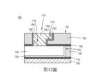
第12圖示出了在特徵770中沉積第二金屬層795之後的第11圖的微電子元件。更具體地,第12圖示出了方法20中的操作26的間隙填充製程。在一些實施例中,沉積第二金屬層795以填充間隙,即特徵770的不由通孔部分772及溝槽部分774界定的部分。第二金屬層795係形成在第一金屬層730的頂表面(通孔部分772的底表面764)上。在一些實施例中,第二金屬層795係形成在金屬襯墊792的頂表面上(例如,頂部上)。第二金屬層795亦可被稱為「間隙填充材料」。在一些實施例中,間隙填充材料包含銅(Cu)、鈷(Co)、鉬(Mo)或釕(Ru)中的一或多者。在一些實施例中,間隙填充材料包含銅(Cu)。在一些實施例中,間隙填充材料由銅(Cu)組成。在一些實施例中,間隙填充材料包含鈷(Co)。在一些實施例中,間隙填充材料由鈷(Co)組成。在一些實施例中,間隙填充材料包含鉬(Mo)。在一些實施例中,間隙填充材料由鉬(Mo)組成。在一些實施例中,間隙填充材料包含釕(Ru)。在一些實施例中,間隙填充材料由釕(Ru)組成。FIG. 12 illustrates the microelectronic device of FIG. 11 after depositing a
在一些實施例中,間隙填充材料包含銅(Cu),金屬襯墊792包含鈷(Co),經處理阻障層790'包含氮化鉭,蝕刻停止層750包含氧化鋁中的一或多者,第二介電層760包含氧化矽,第一金屬層730包含鎢,且第二金屬層795形成在經由特徵770的通孔部分772暴露的第一金屬層730的頂表面上及形成在金屬襯墊792上。In some embodiments, the gap fill material includes copper (Cu), the
在不存在金屬襯墊792的實施例中,第二金屬層795形成在經由特徵770的通孔部分772暴露的第一金屬層730的頂表面上、通孔部分772的側壁762上的經處理阻障層790',以及溝槽部分774的下側壁767、底表面768及上側壁769的經處理阻障層790'上。In an embodiment where the
在一些實施例中,毯敷沉積製程將第二金屬層795沉積到特徵770中且沉積在第二介電層760的頂表面761上。形成在第二介電層760的頂表面761上的第二金屬層795可由任何適合的技術移除,包括但不限於蝕刻及化學機械平坦化(CMP)。In some embodiments, a blanket deposition process deposits the
本揭示案的一或多個實施例係關於一種包括指令的非暫時性電腦可讀媒體,此等指令在由處理腔室的控制器執行時使處理腔室執行方法10的操作。在一些實施例中,非暫時性電腦可讀媒體包括指令,此等指令在由處理腔室的控制器執行時使處理腔室執行方法20的操作。One or more embodiments of the present disclosure relate to a non-transitory computer-readable medium including instructions that, when executed by a controller of a processing chamber, cause the processing chamber to perform the operations of method 10. In some embodiments, the non-transitory computer-readable medium includes instructions that, when executed by a controller of the processing chamber, cause the processing chamber to perform the operations of method 20.
為了便於描述,可在本文中使用諸如「下面」、「下方」及「下部」、「上方」、「上部」及類似者的空間相對術語來描述一個元件或特徵與附加(多個)元件或(多個)特徵的關係,如圖所示。應當理解,空間相對術語旨在涵蓋除了圖中所示的定向之外的在使用或操作中的裝置的不同定向。例如,若圖中的裝置被翻轉,則被描述為處於其他元件或特徵「下方」或「下面」的元件將隨後被定向為處於其他元素或特徵「上方」。因此,例示性術語「下方」可涵蓋上方及下方兩者的定向。裝置可以其他方式定向(旋轉90度或以其他定向),且相應地解釋本文中使用的空間相對描述符。For ease of description, spatially relative terms such as "below," "beneath," and "lower," "above," "upper," and the like may be used herein to describe the relationship of one element or feature to additional element(s) or feature(s), as shown in the figures. It should be understood that spatially relative terms are intended to cover different orientations of the device in use or operation in addition to the orientation shown in the figures. For example, if the device in the figures is flipped, an element described as being "below" or "below" other elements or features will subsequently be oriented to be "above" the other elements or features. Thus, the exemplary term "below" may cover both above and below orientations. The device may be oriented in other ways (rotated 90 degrees or in other orientations), and the spatially relative descriptors used herein are interpreted accordingly.
除非本文另有說明或與上下文明顯衝突,否則在描述本文所討論的材料及方法的上下文中(尤其是在以下發明申請專利範圍的上下文中),術語「一(a/an)」及「該(the)」以及類似參考的使用應被解釋為涵蓋單數及複數兩者。除非本文中另有說明,否則本文中對值的範圍的敘述僅旨在用作個別提及落入此範圍內的每個單獨值的簡寫方法,且每個單獨值被併入說明書中,就如同其在本文中被個別敘述一般。除非本文另有說明或與上下文明顯衝突,否則本文所述的所有方法均可任何適合的次序進行。使用本文提供的任何及所有實例或例示性語言(例如,「諸如」)僅旨在更好地闡明材料及方法,且除非另有主張,否則不對範疇構成限制。說明書中的任何語言均不應被解釋為指示任何未主張的元件對於所揭示的材料及方法的實踐係必不可少的。Unless otherwise indicated herein or clearly contradicted by context, the use of the terms "a", "an", "the" and similar references in the context of describing the materials and methods discussed herein (especially in the context of the following claims) should be construed to cover both the singular and the plural. Unless otherwise indicated herein or clearly contradicted by context, the recitation of ranges of values herein is merely intended to serve as a shorthand method of referring individually to each separate value falling within the range, and each separate value is incorporated into the specification as if it were individually recited herein. All methods described herein can be performed in any suitable order unless otherwise indicated herein or clearly contradicted by context. The use of any and all examples or exemplary language (e.g., "such as") provided herein is intended only to better illustrate the materials and methods and does not constitute a limitation on the scope unless otherwise claimed. No language in the specification should be construed as indicating that any non-claimed element is essential to the practice of the disclosed materials and methods.
在本說明書中,對「一個實施例」、「某些實施例」、「一或多個實施例」或「一實施例」的引用意謂結合實施例描述的特定特徵、結構、材料或特性包括在本揭示案的至少一個實施例中。因此,在本說明書的各個地方,諸如「在一或多個實施例中」、「在某些實施例中」、「在一個實施例中」或「在一實施例中」的片語的出現不一定係指本揭示案的相同實施例。此外,在一或多個實施例中,特定特徵、結構、材料,或特性可以任何適合的方式組合。In this specification, references to "one embodiment", "some embodiments", "one or more embodiments" or "an embodiment" mean that the particular features, structures, materials, or characteristics described in conjunction with the embodiment are included in at least one embodiment of the present disclosure. Therefore, the appearance of phrases such as "in one or more embodiments", "in some embodiments", "in one embodiment" or "in an embodiment" in various places in this specification does not necessarily refer to the same embodiment of the present disclosure. In addition, in one or more embodiments, the particular features, structures, materials, or characteristics may be combined in any suitable manner.
現在參考以下實例描述本揭示案。在描述本揭示案的幾個例示性實施例之前,應當理解,本揭示案不限於以下描述中闡述的構造或製程步驟的細節。本揭示案能夠具有其他實施例且能夠以各種方式實踐或執行。The present disclosure is now described with reference to the following examples. Before describing several exemplary embodiments of the present disclosure, it should be understood that the present disclosure is not limited to the details of the construction or process steps set forth in the following description. The present disclosure is capable of other embodiments and can be practiced or carried out in various ways.
實例Examples
比較實例1Comparison Example 1
將包含氮化鉭(TaN)的阻障層共形地沉積在半導體基板上的介電層上。介電層包含界定間隙的至少一個特徵,此間隙包括包含低k介電材料的側壁及底部。阻障層係以不同的厚度沉積,且用40 MHz的電容耦合電漿(CCP)處理。當以約50 Å、約100 Å及大於100 Å的厚度沉積阻障層時,量測電阻率降低的量。當阻障層經沉積為約50A時,在用CCP 40 MHz處理阻障層30秒後,阻障層顯示出約55%的電阻率降低。當阻障層經沉積為約100 Å時,在用CCP 40 MHz處理阻障層30秒後,阻障層顯示出約49.5%的電阻率降低。當阻障層經沉積為大於100 Å(約170 Å)時,在用CCP 40 MHz處理阻障層30秒後,阻障層顯示出約40.6%的電阻率降低。A barrier layer comprising tantalum nitride (TaN) is conformally deposited on a dielectric layer on a semiconductor substrate. The dielectric layer comprises at least one feature defining a gap, the gap comprising sidewalls and a bottom comprising a low-k dielectric material. The barrier layer is deposited at different thicknesses and processed with a capacitively coupled plasma (CCP) at 40 MHz. The amount of resistivity reduction is measured when the barrier layer is deposited at a thickness of about 50 Å, about 100 Å, and greater than 100 Å. When the barrier layer is deposited at about 50 Å, the barrier layer shows a resistivity reduction of about 55% after the barrier layer is processed with CCP 40 MHz for 30 seconds. When the barrier layer was deposited to about 100 Å, the barrier layer showed a resistivity reduction of about 49.5% after the barrier layer was treated with CCP 40 MHz for 30 seconds. When the barrier layer was deposited to greater than 100 Å (about 170 Å), the barrier layer showed a resistivity reduction of about 40.6% after the barrier layer was treated with CCP 40 MHz for 30 seconds.
比較實例2Comparison Example 2
將包含氮化鉭(TaN)的阻障層共形地沉積在半導體基板上的介電層上。介電層包含界定間隙的至少一個特徵,此間隙包括包含低k介電材料的側壁及底部。阻障層係以不同的厚度沉積,且用40 MHz的電容耦合電漿(CCP)處理。當用40 MHz CCP處理阻障層30秒時,量測低k損傷量及碳(C)損失量。藉由使用熟習此項技術者已知的汞(Hg)探針技術量測經處理阻障層的介電常數來量測低k損傷量。通常,觀察到介電常數越高,存在的低k損傷量越大。用40 MHz CCP處理30秒的阻障層的介電常數經量測為約3.68。作為用40 MHz CCP處理30秒的結果,存在約16%的碳損失(使用X射線光電子光譜法(x-ray photoelectron spectroscopy, XPS)量測)。A barrier layer comprising tantalum nitride (TaN) is conformally deposited on a dielectric layer on a semiconductor substrate. The dielectric layer comprises at least one feature defining a gap, the gap comprising sidewalls and a bottom comprising a low-k dielectric material. The barrier layer is deposited at different thicknesses and processed using a 40 MHz capacitively coupled plasma (CCP). The amount of low-k damage and carbon (C) loss is measured when the barrier layer is treated with a 40 MHz CCP for 30 seconds. The amount of low-k damage is measured by measuring the dielectric constant of the treated barrier layer using a mercury (Hg) probe technique known to those skilled in the art. In general, it is observed that the higher the dielectric constant, the greater the amount of low-k damage present. The dielectric constant of the barrier layer treated with 40 MHz CCP for 30 seconds was measured to be about 3.68. As a result of the 40 MHz CCP treatment for 30 seconds, there was about 16% carbon loss (measured using x-ray photoelectron spectroscopy (XPS)).
本發明實例1Example 1 of the present invention
將包含氮化鉭(TaN)的阻障層共形地沉積在半導體基板上的介電層上。介電層包含界定間隙的至少一個特徵,此間隙包括包含低k介電材料的側壁及底部。阻障層係以不同厚度沉積,且根據方法10及20用微波輻射處理。當以約50 Å、約100 Å及大於100 Å的厚度沉積阻障層時,量測電阻率降低的量。當阻障層經沉積到約50 Å時,在用微波輻射處理阻障層總共10分鐘之後,阻障層顯示出約77%的電阻率降低。當阻障層經沉積為約100 Å時,在用微波輻射處理阻障層總共10分鐘之後,阻障層顯示出約51%的電阻率降低。當以大於100 Å(至約170 Å)的厚度沉積阻障層時,在用微波輻射處理阻障層總共10分鐘之後,阻障層顯示出約38%的電阻率降低。有利地,用微波輻射處理阻障層可實現比包括用40 MHz CCP處理阻障層30秒的比較實例1實現的更大的電阻率降低(降低至少15%或至少20%)。A barrier layer comprising tantalum nitride (TaN) is conformally deposited on a dielectric layer on a semiconductor substrate. The dielectric layer comprises at least one feature defining a gap, the gap comprising sidewalls and a bottom comprising a low-k dielectric material. The barrier layer is deposited at different thicknesses and treated with microwave radiation according to methods 10 and 20. The amount of resistivity reduction is measured when the barrier layer is deposited at a thickness of about 50 Å, about 100 Å, and greater than 100 Å. When the barrier layer is deposited to about 50 Å, the barrier layer shows a resistivity reduction of about 77% after treating the barrier layer with microwave radiation for a total of 10 minutes. When the barrier layer is deposited to be about 100 Å, the barrier layer exhibits a resistivity reduction of about 51% after the barrier layer is treated with microwave radiation for a total of 10 minutes. When the barrier layer is deposited to a thickness greater than 100 Å (to about 170 Å), the barrier layer exhibits a resistivity reduction of about 38% after the barrier layer is treated with microwave radiation for a total of 10 minutes. Advantageously, treating the barrier layer with microwave radiation can achieve a greater resistivity reduction (at least 15% or at least 20%) than that achieved in Comparative Example 1, which includes treating the barrier layer with a 40 MHz CCP for 30 seconds.
本發明實例2Example 2 of the present invention
將包含氮化鉭(TaN)的阻障層共形地沉積在半導體基板上的介電層上。介電層包含界定間隙的至少一個特徵,此間隙包括包含低k介電材料的側壁及底部。阻障層係以不同厚度沉積,且根據方法10及20用微波輻射處理。A barrier layer comprising tantalum nitride (TaN) is conformally deposited on a dielectric layer on a semiconductor substrate. The dielectric layer comprises at least one feature defining a gap, the gap comprising sidewalls and a bottom comprising a low-k dielectric material. The barrier layer is deposited at different thicknesses and treated with microwave radiation according to methods 10 and 20.
當用微波輻射處理阻障層1分鐘及5分鐘時,量測低k損傷量。藉由使用熟習此項技術者已知的汞(Hg)探針技術量測經處理阻障層的介電常數來量測低k損傷量。通常,觀察到介電常數越高,存在的低k損傷量越大。用微波輻射處理1分鐘的阻障層的介電常數經量測為約3.15。用微波輻射處理5分鐘的阻障層的介電常數經量測為約3.18。The amount of low-k damage was measured when the barrier layer was treated with microwave radiation for 1 minute and 5 minutes. The amount of low-k damage was measured by measuring the dielectric constant of the treated barrier layer using a mercury (Hg) probe technique known to those skilled in the art. In general, it was observed that the higher the dielectric constant, the greater the amount of low-k damage present. The dielectric constant of the barrier layer treated with microwave radiation for 1 minute was measured to be approximately 3.15. The dielectric constant of the barrier layer treated with microwave radiation for 5 minutes was measured to be approximately 3.18.
當用微波輻射處理阻障層1分鐘、3分鐘、5分鐘及10分鐘時,使用X射線光電子光譜法(XPS)量測碳(C)損失量。作為用微波輻射處理1分鐘的結果,存在小於1%的碳損失。作為用微波輻射處理3分鐘的結果,存在小於1.2%的碳損失。作為用微波輻射處理1分鐘的結果,存在小於1.5%的碳損失。作為用微波輻射處理1分鐘的結果,存在小於3.3%的碳損失。有利地,與用40 MHz CCP處理30秒相比,用微波輻射處理阻障層導致更少的低k損傷及更少的碳(C)損失。The amount of carbon (C) loss was measured using X-ray photoelectron spectroscopy (XPS) when the barrier layer was treated with microwave irradiation for 1 minute, 3 minutes, 5 minutes, and 10 minutes. As a result of the treatment with microwave irradiation for 1 minute, there was less than 1% carbon loss. As a result of the treatment with microwave irradiation for 3 minutes, there was less than 1.2% carbon loss. As a result of the treatment with microwave irradiation for 1 minute, there was less than 1.5% carbon loss. As a result of the treatment with microwave irradiation for 1 minute, there was less than 3.3% carbon loss. Advantageously, treating the barrier layer with microwave irradiation results in less low-k damage and less carbon (C) loss than treating with a 40 MHz CCP for 30 seconds.
儘管已參考特定實施例描述了本文的揭示內容,但熟習此項技術者將理解,所描述的實施例僅為本揭示案的原理及應用的說明。對熟習此項技術者來說顯而易見的為,在不脫離本揭示案的精神及範疇的情況下,可對本揭示案的方法及裝置進行各種修改及變化。因此,本揭示案可包括在所附發明申請專利範圍及其等效物的範疇內的修改及變化。Although the disclosure herein has been described with reference to specific embodiments, it will be understood by those skilled in the art that the described embodiments are merely illustrative of the principles and applications of the disclosure. It will be apparent to those skilled in the art that various modifications and variations may be made to the methods and apparatus of the disclosure without departing from the spirit and scope of the disclosure. Therefore, the disclosure may include modifications and variations within the scope of the appended invention claims and their equivalents.
10:方法 12:操作 14:操作 20:方法 21:操作 22:操作 23:操作 24:操作 25:操作 26:操作 100:處理工具 104:模組化高頻發射源 105:高頻發射模組 106:振盪器模組 130:放大模組 142:施用器 150:源陣列 170:氣體管線 172:排放管線 174:基板 176:卡盤 178:半導體處理腔室 210:電壓控制電路 220:壓控振盪器 221:控制電路模組 234:前置放大器 236:主功率放大器 238:循環器 239:電源供應器 249:隔熱件 281:偵測器模組 282:反射功率 283:前向功率 285:控制信號 286:控制信號 350:源陣列 360:介電板 366:介電共振器 370:組件 372:外殼 373:導電主體 374:開口 450:源陣列 460:介電板 461:第一表面 462:第二表面 465:孔 466:介電共振器 467:腔 500:處理工具 574:工件 576:卡盤 578:半導體處理腔室 581:O形環 582:電漿 583:內部容積 588:單極天線 700:微電子元件 705:基板 710:第一層 720:襯墊 730:第一金屬層 732:頂表面 740:第一介電層 742:內側壁 750:蝕刻停止層 760:第二介電層 761:頂表面 762:側壁 763:側壁 764:底表面 767:下側壁 768:底表面 769:上側壁 770:特徵 772:通孔部分 774:溝槽部分 780:阻擋層 790:阻障層 790':經處理阻障層 792:金屬襯墊 795:第二金屬層 D:深度 G:間隙 W1:第一寬度 W2:第二寬度10: Method 12: Operation 14: Operation 20: Method 21: Operation 22: Operation 23: Operation 24: Operation 25: Operation 26: Operation 100: Processing tool 104: Modular high frequency emission source 105: High frequency emission module 106: Oscillator module 130: Amplification module 142: Applicator 150: Source array 170: Gas pipeline 172: Exhaust pipeline 174: Substrate 176: Chuck 178: Semiconductor processing chamber 210: Voltage control circuit 220: voltage controlled oscillator 221: control circuit module 234: preamplifier 236: main power amplifier 238: circulator 239: power supply 249: thermal insulation 281: detector module 282: reflected power 283: forward power 285: control signal 286: control signal 350: source array 360: dielectric plate 366: dielectric resonator 370: assembly 372: housing 373: conductive body 374: Opening 450: source array 460: dielectric plate 461: first surface 462: second surface 465: hole 466: dielectric resonator 467: cavity 500: processing tool 574: workpiece 576: chuck 578: semiconductor processing chamber 581: O-ring 582: plasma 583: internal volume 588: monopole antenna 700: microelectronic component 705: substrate 710: first layer 720: pad 730: first metal layer 732: top surface Surface 740: first dielectric layer 742: inner sidewall 750: etch stop layer 760: second dielectric layer 761: top surface 762: sidewall 763: sidewall 764: bottom surface 767: lower sidewall 768: bottom surface 769: upper sidewall 770: feature 772: through hole portion 774: trench portion 780: blocking layer 790: barrier layer 790': treated barrier layer 792: metal liner 795: second metal layer D: depth G: gapW1 : first widthW2 : second width
為了詳細理解本揭示案的上述特徵,可參考實施例對上文簡要概述的本揭示案進行更具體的描述,此等實施例中的一些在隨附圖式中示出。然而,應當註意,隨附圖式僅示出了本揭示案的典型實施例,因此不應被認為係對其範疇的限制,因為本揭示案可允許其他同樣有效的實施例。In order to understand the above features of the present disclosure in detail, the present disclosure briefly summarized above will be described in more detail with reference to the embodiments, some of which are shown in the accompanying drawings. However, it should be noted that the accompanying drawings only show typical embodiments of the present disclosure and should not be considered as limiting the scope thereof, because the present disclosure may allow other equally effective embodiments.
第1圖示出了根據本揭示案的一或多個實施例的處理工具的示意圖,此處理工具包含具有源陣列的模組化高頻發射源,此源陣列包含複數個施用器;FIG. 1 is a schematic diagram of a processing tool according to one or more embodiments of the present disclosure, the processing tool comprising a modular high frequency emission source having a source array, the source array comprising a plurality of applicators;
第2圖示出了根據本揭示案的一或多個實施例的模組化高頻發射模組的方塊圖;FIG. 2 shows a block diagram of a modular high frequency transmit module according to one or more embodiments of the present disclosure;
第3圖示出了根據本揭示案的一或多個實施例的組件的示意性分解透視圖;FIG. 3 shows a schematic exploded perspective view of components according to one or more embodiments of the present disclosure;
第4圖示出了根據一或多個實施例的在介電板中的腔中具有介電共振器的源陣列的示意性透視圖;FIG. 4 illustrates a schematic perspective view of a source array having dielectric resonators in cavities in a dielectric slab according to one or more embodiments;
第5圖示出了根據一或多個實施例的處理工具的橫截面圖;FIG. 5 illustrates a cross-sectional view of a processing tool according to one or more embodiments;
第6A圖示出了根據本揭示案的一或多個實施例的形成微電子元件的方法的製程流程圖;FIG. 6A is a process flow diagram illustrating a method of forming a microelectronic device according to one or more embodiments of the present disclosure;
第6B圖示出了根據本揭示案的一或多個實施例的形成微電子元件的方法的製程流程圖;FIG. 6B is a process flow diagram illustrating a method of forming a microelectronic device according to one or more embodiments of the present disclosure;
第7圖示出了根據本揭示案的一或多個實施例的選擇性沉積製程之前的微電子元件的橫截面示意圖;FIG. 7 is a schematic cross-sectional view of a microelectronic device prior to a selective deposition process according to one or more embodiments of the present disclosure;
第8圖示出了根據本揭示案的一或多個實施例的形成阻擋層之後的第7圖的微電子元件的橫截面示意圖;FIG. 8 is a schematic cross-sectional view of the microelectronic device of FIG. 7 after forming a barrier layer according to one or more embodiments of the present disclosure;
第9圖示出了根據本揭示案的一或多個實施例的形成阻障層之後的第8圖的微電子元件的橫截面示意圖;FIG. 9 is a schematic cross-sectional view of the microelectronic device of FIG. 8 after forming a barrier layer according to one or more embodiments of the present disclosure;
第10A圖示出了根據本揭示案的一或多個實施例的處理阻障層以形成經處理阻障層之後的第9圖的微電子元件的橫截面示意圖;FIG. 10A is a schematic cross-sectional view of the microelectronic device of FIG. 9 after processing the barrier layer to form a processed barrier layer according to one or more embodiments of the present disclosure;
第10B圖示出了根據本揭示案的一或多個實施例的移除阻擋層之後的第10A圖的微電子元件的橫截面示意圖;FIG. 10B is a schematic cross-sectional view of the microelectronic device of FIG. 10A after removing the barrier layer according to one or more embodiments of the present disclosure;
第11圖示出了根據本揭示案的一或多個實施例的形成金屬襯墊之後的第10B圖的微電子元件的橫截面示意圖;及FIG. 11 is a schematic cross-sectional view of the microelectronic device of FIG. 10B after forming a metal pad according to one or more embodiments of the present disclosure; and
第12圖示出了根據本揭示案的一或多個實施例的形成第二金屬層之後的第11圖的微電子元件的橫截面示意圖。FIG. 12 illustrates a schematic cross-sectional view of the microelectronic device of FIG. 11 after forming a second metal layer according to one or more embodiments of the present disclosure.
為了便於理解,在可能的情況下,使用相同的元件符號來指定附圖中共同的相同元件。考慮到,一個實施例的元件及特徵可有利地結合在其他實施例中而無需進一步闡述。To facilitate understanding, identical reference numerals have been used, where possible, to designate identical elements that are common to the figures. It is contemplated that elements and features of one embodiment may be beneficially combined in other embodiments without further recitation.
國內寄存資訊(請依寄存機構、日期、號碼順序註記) 無 國外寄存資訊(請依寄存國家、機構、日期、號碼順序註記) 無Domestic storage information (please note in the order of storage institution, date, and number)NoneForeign storage information (please note in the order of storage country, institution, date, and number)None
20:方法20: Methods
21:操作21: Operation
22:操作22: Operation
23:操作23: Operation
24:操作24: Operation
25:操作25: Operation
26:操作26: Operation
Claims (20)
Translated fromChineseApplications Claiming Priority (2)
| Application Number | Priority Date | Filing Date | Title |
|---|---|---|---|
| US202363525848P | 2023-07-10 | 2023-07-10 | |
| US63/525,848 | 2023-07-10 |
Publications (1)
| Publication Number | Publication Date |
|---|---|
| TW202503924Atrue TW202503924A (en) | 2025-01-16 |
Family
ID=94210606
Family Applications (1)
| Application Number | Title | Priority Date | Filing Date |
|---|---|---|---|
| TW113120941ATW202503924A (en) | 2023-07-10 | 2024-06-06 | Methods of forming interconnect structures |
Country Status (3)
| Country | Link |
|---|---|
| US (1) | US20250022750A1 (en) |
| TW (1) | TW202503924A (en) |
| WO (1) | WO2025014640A1 (en) |
Family Cites Families (5)
| Publication number | Priority date | Publication date | Assignee | Title |
|---|---|---|---|---|
| TW201044462A (en)* | 2009-01-22 | 2010-12-16 | Tokyo Electron Ltd | A method for manufacturing semiconductor devices |
| US8716132B2 (en)* | 2009-02-13 | 2014-05-06 | Tokyo Electron Limited | Radiation-assisted selective deposition of metal-containing cap layers |
| US9583386B2 (en)* | 2014-10-25 | 2017-02-28 | Lam Research Corporation | Interlevel conductor pre-fill utilizing selective barrier deposition |
| US10822692B2 (en)* | 2016-08-12 | 2020-11-03 | University Of North Texas | Binary Ag—Cu amorphous thin-films for electronic applications |
| US12211743B2 (en)* | 2021-09-03 | 2025-01-28 | Applied Materials, Inc. | Method of forming a metal liner for interconnect structures |
- 2024
- 2024-06-06TWTW113120941Apatent/TW202503924A/enunknown
- 2024-06-24WOPCT/US2024/035187patent/WO2025014640A1/enactivePending
- 2024-06-25USUS18/753,020patent/US20250022750A1/enactivePending
Also Published As
| Publication number | Publication date |
|---|---|
| WO2025014640A1 (en) | 2025-01-16 |
| US20250022750A1 (en) | 2025-01-16 |
Similar Documents
| Publication | Publication Date | Title |
|---|---|---|
| KR102549289B1 (en) | Method of selective deposition for forming fully self-aligned vias | |
| JP6962955B2 (en) | How to enable seamless cobalt gap filling | |
| JP4503356B2 (en) | Substrate processing method and semiconductor device manufacturing method | |
| CN110066984B (en) | A method to achieve seamless cobalt gap filling | |
| TWI630654B (en) | Recessing ultra-low k dielectric using remote plasma source | |
| US7919142B2 (en) | Atomic layer deposition apparatus using neutral beam and method of depositing atomic layer using the same | |
| WO2005045916A1 (en) | Method for processing substrate | |
| US11024537B2 (en) | Methods and apparatus for hybrid feature metallization | |
| TW202503924A (en) | Methods of forming interconnect structures | |
| US20250253192A1 (en) | Barrier and liner treatment using dual radio frequency capacitive couple plasma for metal interconnects | |
| US20240222192A1 (en) | Selective metal selectivity improvement with rf pulsing | |
| TWI505360B (en) | Method of forming metal carbide barrier layers for fluorocarbon films | |
| US20240191353A1 (en) | Electrochemical reduction of surface metal oxides | |
| TWI899549B (en) | Method of selective deposition for forming fully self-aligned vias | |
| US20250087477A1 (en) | Methods of forming silicon nitride films | |
| TW202534762A (en) | Coetaneous deposition and etch for bottom-up carbon gapfill |