TW202501718A - Semiconductor structure - Google Patents
Semiconductor structureDownload PDFInfo
- Publication number
- TW202501718A TW202501718ATW112129480ATW112129480ATW202501718ATW 202501718 ATW202501718 ATW 202501718ATW 112129480 ATW112129480 ATW 112129480ATW 112129480 ATW112129480 ATW 112129480ATW 202501718 ATW202501718 ATW 202501718A
- Authority
- TW
- Taiwan
- Prior art keywords
- source
- gate
- drain
- feature
- isolation structure
- Prior art date
Links
- 239000004065semiconductorSubstances0.000titleclaimsabstractdescription82
- 229910052751metalInorganic materials0.000claimsabstractdescription174
- 239000002184metalSubstances0.000claimsabstractdescription174
- 238000002955isolationMethods0.000claimsabstractdescription171
- 239000000758substrateSubstances0.000claimsabstractdescription28
- 125000006850spacer groupChemical group0.000claimsdescription78
- 239000003989dielectric materialSubstances0.000claimsdescription18
- 238000000034methodMethods0.000abstractdescription84
- 239000010410layerSubstances0.000description105
- 230000036961partial effectEffects0.000description47
- 230000008569processEffects0.000description46
- 238000005530etchingMethods0.000description29
- 239000000463materialSubstances0.000description26
- XUIMIQQOPSSXEZ-UHFFFAOYSA-NSiliconChemical compound[Si]XUIMIQQOPSSXEZ-UHFFFAOYSA-N0.000description16
- 238000004519manufacturing processMethods0.000description16
- 229910052710siliconInorganic materials0.000description16
- 239000010703siliconSubstances0.000description16
- 238000005229chemical vapour depositionMethods0.000description13
- 229910052581Si3N4Inorganic materials0.000description12
- VYPSYNLAJGMNEJ-UHFFFAOYSA-NSilicium dioxideChemical compoundO=[Si]=OVYPSYNLAJGMNEJ-UHFFFAOYSA-N0.000description12
- 230000015572biosynthetic processEffects0.000description12
- 229910021332silicideInorganic materials0.000description12
- HQVNEWCFYHHQES-UHFFFAOYSA-Nsilicon nitrideChemical compoundN12[Si]34N5[Si]62N3[Si]51N64HQVNEWCFYHHQES-UHFFFAOYSA-N0.000description12
- FVBUAEGBCNSCDD-UHFFFAOYSA-Nsilicide(4-)Chemical compound[Si-4]FVBUAEGBCNSCDD-UHFFFAOYSA-N0.000description11
- 238000000151depositionMethods0.000description10
- 229910052814silicon oxideInorganic materials0.000description10
- 238000000231atomic layer depositionMethods0.000description9
- 230000004888barrier functionEffects0.000description9
- 238000005240physical vapour depositionMethods0.000description7
- 239000002019doping agentSubstances0.000description6
- 238000001459lithographyMethods0.000description6
- 229910052782aluminiumInorganic materials0.000description5
- 230000002829reductive effectEffects0.000description5
- MCMNRKCIXSYSNV-UHFFFAOYSA-NZirconium dioxideChemical compoundO=[Zr]=OMCMNRKCIXSYSNV-UHFFFAOYSA-N0.000description4
- XAGFODPZIPBFFR-UHFFFAOYSA-NaluminiumChemical compound[Al]XAGFODPZIPBFFR-UHFFFAOYSA-N0.000description4
- 230000008901benefitEffects0.000description4
- 238000005137deposition processMethods0.000description4
- 238000001312dry etchingMethods0.000description4
- TWNQGVIAIRXVLR-UHFFFAOYSA-Noxo(oxoalumanyloxy)alumaneChemical compoundO=[Al]O[Al]=OTWNQGVIAIRXVLR-UHFFFAOYSA-N0.000description4
- 229920002120photoresistant polymerPolymers0.000description4
- ZOXJGFHDIHLPTG-UHFFFAOYSA-NBoronChemical compound[B]ZOXJGFHDIHLPTG-UHFFFAOYSA-N0.000description3
- KRHYYFGTRYWZRS-UHFFFAOYSA-NFluoraneChemical compoundFKRHYYFGTRYWZRS-UHFFFAOYSA-N0.000description3
- 229910000577Silicon-germaniumInorganic materials0.000description3
- QVGXLLKOCUKJST-UHFFFAOYSA-Natomic oxygenChemical compound[O]QVGXLLKOCUKJST-UHFFFAOYSA-N0.000description3
- 229910052796boronInorganic materials0.000description3
- 239000010949copperSubstances0.000description3
- 238000005516engineering processMethods0.000description3
- 239000000203mixtureSubstances0.000description3
- 239000002086nanomaterialSubstances0.000description3
- 239000002135nanosheetSubstances0.000description3
- 239000001301oxygenSubstances0.000description3
- 229910052760oxygenInorganic materials0.000description3
- 238000000623plasma-assisted chemical vapour depositionMethods0.000description3
- HBMJWWWQQXIZIP-UHFFFAOYSA-Nsilicon carbideChemical compound[Si+]#[C-]HBMJWWWQQXIZIP-UHFFFAOYSA-N0.000description3
- 229910052715tantalumInorganic materials0.000description3
- 229910052721tungstenInorganic materials0.000description3
- 238000001039wet etchingMethods0.000description3
- XKRFYHLGVUSROY-UHFFFAOYSA-NArgonChemical compound[Ar]XKRFYHLGVUSROY-UHFFFAOYSA-N0.000description2
- JBRZTFJDHDCESZ-UHFFFAOYSA-NAsGaChemical compound[As]#[Ga]JBRZTFJDHDCESZ-UHFFFAOYSA-N0.000description2
- HEDRZPFGACZZDS-UHFFFAOYSA-NChloroformChemical compoundClC(Cl)ClHEDRZPFGACZZDS-UHFFFAOYSA-N0.000description2
- RYGMFSIKBFXOCR-UHFFFAOYSA-NCopperChemical compound[Cu]RYGMFSIKBFXOCR-UHFFFAOYSA-N0.000description2
- 229910000530Gallium indium arsenideInorganic materials0.000description2
- GPXJNWSHGFTCBW-UHFFFAOYSA-NIndium phosphideChemical compound[In]#PGPXJNWSHGFTCBW-UHFFFAOYSA-N0.000description2
- PXHVJJICTQNCMI-UHFFFAOYSA-NNickelChemical compound[Ni]PXHVJJICTQNCMI-UHFFFAOYSA-N0.000description2
- KDLHZDBZIXYQEI-UHFFFAOYSA-NPalladiumChemical compound[Pd]KDLHZDBZIXYQEI-UHFFFAOYSA-N0.000description2
- OAICVXFJPJFONN-UHFFFAOYSA-NPhosphorusChemical compound[P]OAICVXFJPJFONN-UHFFFAOYSA-N0.000description2
- -1TaAlCInorganic materials0.000description2
- BOTDANWDWHJENH-UHFFFAOYSA-NTetraethyl orthosilicateChemical compoundCCO[Si](OCC)(OCC)OCCBOTDANWDWHJENH-UHFFFAOYSA-N0.000description2
- ATJFFYVFTNAWJD-UHFFFAOYSA-NTinChemical compound[Sn]ATJFFYVFTNAWJD-UHFFFAOYSA-N0.000description2
- XLOMVQKBTHCTTD-UHFFFAOYSA-NZinc monoxideChemical compound[Zn]=OXLOMVQKBTHCTTD-UHFFFAOYSA-N0.000description2
- KXNLCSXBJCPWGL-UHFFFAOYSA-N[Ga].[As].[In]Chemical compound[Ga].[As].[In]KXNLCSXBJCPWGL-UHFFFAOYSA-N0.000description2
- LEVVHYCKPQWKOP-UHFFFAOYSA-N[Si].[Ge]Chemical compound[Si].[Ge]LEVVHYCKPQWKOP-UHFFFAOYSA-N0.000description2
- FTWRSWRBSVXQPI-UHFFFAOYSA-Nalumanylidynearsane;gallanylidynearsaneChemical compound[As]#[Al].[As]#[Ga]FTWRSWRBSVXQPI-UHFFFAOYSA-N0.000description2
- 229910052785arsenicInorganic materials0.000description2
- RQNWIZPPADIBDY-UHFFFAOYSA-Narsenic atomChemical compound[As]RQNWIZPPADIBDY-UHFFFAOYSA-N0.000description2
- 239000005380borophosphosilicate glassSubstances0.000description2
- DIKBFYAXUHHXCS-UHFFFAOYSA-NbromoformChemical compoundBrC(Br)BrDIKBFYAXUHHXCS-UHFFFAOYSA-N0.000description2
- 229910017052cobaltInorganic materials0.000description2
- 239000010941cobaltSubstances0.000description2
- GUTLYIVDDKVIGB-UHFFFAOYSA-Ncobalt atomChemical compound[Co]GUTLYIVDDKVIGB-UHFFFAOYSA-N0.000description2
- 239000004020conductorSubstances0.000description2
- 229910052802copperInorganic materials0.000description2
- 230000003247decreasing effectEffects0.000description2
- 230000008021depositionEffects0.000description2
- 238000009713electroplatingMethods0.000description2
- 229910052732germaniumInorganic materials0.000description2
- GNPVGFCGXDBREM-UHFFFAOYSA-Ngermanium atomChemical compound[Ge]GNPVGFCGXDBREM-UHFFFAOYSA-N0.000description2
- 230000000670limiting effectEffects0.000description2
- 239000002070nanowireSubstances0.000description2
- 230000003647oxidationEffects0.000description2
- 238000007254oxidation reactionMethods0.000description2
- BPUBBGLMJRNUCC-UHFFFAOYSA-Noxygen(2-);tantalum(5+)Chemical compound[O-2].[O-2].[O-2].[O-2].[O-2].[Ta+5].[Ta+5]BPUBBGLMJRNUCC-UHFFFAOYSA-N0.000description2
- 238000000059patterningMethods0.000description2
- 229910052698phosphorusInorganic materials0.000description2
- 239000011574phosphorusSubstances0.000description2
- 239000005360phosphosilicate glassSubstances0.000description2
- 238000001020plasma etchingMethods0.000description2
- 239000005368silicate glassSubstances0.000description2
- 229910010271silicon carbideInorganic materials0.000description2
- 239000002356single layerSubstances0.000description2
- 239000000126substanceSubstances0.000description2
- GUVRBAGPIYLISA-UHFFFAOYSA-Ntantalum atomChemical compound[Ta]GUVRBAGPIYLISA-UHFFFAOYSA-N0.000description2
- 229910001936tantalum oxideInorganic materials0.000description2
- VZGDMQKNWNREIO-UHFFFAOYSA-NtetrachloromethaneChemical compoundClC(Cl)(Cl)ClVZGDMQKNWNREIO-UHFFFAOYSA-N0.000description2
- 239000010936titaniumSubstances0.000description2
- WFKWXMTUELFFGS-UHFFFAOYSA-NtungstenChemical compound[W]WFKWXMTUELFFGS-UHFFFAOYSA-N0.000description2
- 239000010937tungstenSubstances0.000description2
- ZVWKZXLXHLZXLS-UHFFFAOYSA-Nzirconium nitrideChemical compound[Zr]#NZVWKZXLXHLZXLS-UHFFFAOYSA-N0.000description2
- ZXEYZECDXFPJRJ-UHFFFAOYSA-N$l^{3}-silane;platinumChemical compound[SiH3].[Pt]ZXEYZECDXFPJRJ-UHFFFAOYSA-N0.000description1
- WEAMLHXSIBDPGN-UHFFFAOYSA-N(4-hydroxy-3-methylphenyl) thiocyanateChemical compoundCC1=CC(SC#N)=CC=C1OWEAMLHXSIBDPGN-UHFFFAOYSA-N0.000description1
- ITWBWJFEJCHKSN-UHFFFAOYSA-N1,4,7-triazonaneChemical compoundC1CNCCNCCN1ITWBWJFEJCHKSN-UHFFFAOYSA-N0.000description1
- ZCYVEMRRCGMTRW-UHFFFAOYSA-N7553-56-2Chemical compound[I]ZCYVEMRRCGMTRW-UHFFFAOYSA-N0.000description1
- 229910015844BCl3Inorganic materials0.000description1
- WKBOTKDWSSQWDR-UHFFFAOYSA-NBromine atomChemical compound[Br]WKBOTKDWSSQWDR-UHFFFAOYSA-N0.000description1
- OKTJSMMVPCPJKN-UHFFFAOYSA-NCarbonChemical compound[C]OKTJSMMVPCPJKN-UHFFFAOYSA-N0.000description1
- KZBUYRJDOAKODT-UHFFFAOYSA-NChlorineChemical compoundClClKZBUYRJDOAKODT-UHFFFAOYSA-N0.000description1
- ZAMOUSCENKQFHK-UHFFFAOYSA-NChlorine atomChemical compound[Cl]ZAMOUSCENKQFHK-UHFFFAOYSA-N0.000description1
- 229910052691ErbiumInorganic materials0.000description1
- YCKRFDGAMUMZLT-UHFFFAOYSA-NFluorine atomChemical compound[F]YCKRFDGAMUMZLT-UHFFFAOYSA-N0.000description1
- XPDWGBQVDMORPB-UHFFFAOYSA-NFluoroformChemical compoundFC(F)FXPDWGBQVDMORPB-UHFFFAOYSA-N0.000description1
- GYHNNYVSQQEPJS-UHFFFAOYSA-NGalliumChemical compound[Ga]GYHNNYVSQQEPJS-UHFFFAOYSA-N0.000description1
- 229910001218Gallium arsenideInorganic materials0.000description1
- JMASRVWKEDWRBT-UHFFFAOYSA-NGallium nitrideChemical compound[Ga]#NJMASRVWKEDWRBT-UHFFFAOYSA-N0.000description1
- 229910000673Indium arsenideInorganic materials0.000description1
- 229910020968MoSi2Inorganic materials0.000description1
- 229910012990NiSi2Inorganic materials0.000description1
- BPQQTUXANYXVAA-UHFFFAOYSA-NOrthosilicateChemical compound[O-][Si]([O-])([O-])[O-]BPQQTUXANYXVAA-UHFFFAOYSA-N0.000description1
- KJTLSVCANCCWHF-UHFFFAOYSA-NRutheniumChemical compound[Ru]KJTLSVCANCCWHF-UHFFFAOYSA-N0.000description1
- 229910004490TaAlInorganic materials0.000description1
- 229910004217TaSi2Inorganic materials0.000description1
- 229910004200TaSiNInorganic materials0.000description1
- 229910010037TiAlNInorganic materials0.000description1
- GWEVSGVZZGPLCZ-UHFFFAOYSA-NTitan oxideChemical compoundO=[Ti]=OGWEVSGVZZGPLCZ-UHFFFAOYSA-N0.000description1
- 229910052770UraniumInorganic materials0.000description1
- HMDDXIMCDZRSNE-UHFFFAOYSA-N[C].[Si]Chemical compound[C].[Si]HMDDXIMCDZRSNE-UHFFFAOYSA-N0.000description1
- WZECUPJJEIXUKY-UHFFFAOYSA-N[O-2].[O-2].[O-2].[U+6]Chemical compound[O-2].[O-2].[O-2].[U+6]WZECUPJJEIXUKY-UHFFFAOYSA-N0.000description1
- 239000012790adhesive layerSubstances0.000description1
- AJGDITRVXRPLBY-UHFFFAOYSA-Naluminum indiumChemical compound[Al].[In]AJGDITRVXRPLBY-UHFFFAOYSA-N0.000description1
- HVXCTUSYKCFNMG-UHFFFAOYSA-Naluminum oxygen(2-) zirconium(4+)Chemical compound[O-2].[Zr+4].[Al+3]HVXCTUSYKCFNMG-UHFFFAOYSA-N0.000description1
- 230000003466anti-cipated effectEffects0.000description1
- 229910052786argonInorganic materials0.000description1
- GDTBXPJZTBHREO-UHFFFAOYSA-NbromineSubstancesBrBrGDTBXPJZTBHREO-UHFFFAOYSA-N0.000description1
- 229910052794bromiumInorganic materials0.000description1
- 229910052799carbonInorganic materials0.000description1
- 239000000460chlorineSubstances0.000description1
- 229910052801chlorineInorganic materials0.000description1
- 238000004140cleaningMethods0.000description1
- 229910052681coesiteInorganic materials0.000description1
- 230000000295complement effectEffects0.000description1
- PMHQVHHXPFUNSP-UHFFFAOYSA-Mcopper(1+);methylsulfanylmethane;bromideChemical compoundBr[Cu].CSCPMHQVHHXPFUNSP-UHFFFAOYSA-M0.000description1
- 230000008878couplingEffects0.000description1
- 238000010168coupling processMethods0.000description1
- 238000005859coupling reactionMethods0.000description1
- 229910052906cristobaliteInorganic materials0.000description1
- 238000009792diffusion processMethods0.000description1
- RWRIWBAIICGTTQ-UHFFFAOYSA-NdifluoromethaneChemical compoundFCFRWRIWBAIICGTTQ-UHFFFAOYSA-N0.000description1
- 230000000694effectsEffects0.000description1
- UYAHIZSMUZPPFV-UHFFFAOYSA-NerbiumChemical compound[Er]UYAHIZSMUZPPFV-UHFFFAOYSA-N0.000description1
- 230000005669field effectEffects0.000description1
- 230000009969flowable effectEffects0.000description1
- 229910052731fluorineInorganic materials0.000description1
- 239000011737fluorineSubstances0.000description1
- 239000012634fragmentSubstances0.000description1
- 229910052733galliumInorganic materials0.000description1
- HZXMRANICFIONG-UHFFFAOYSA-Ngallium phosphideChemical compound[Ga]#PHZXMRANICFIONG-UHFFFAOYSA-N0.000description1
- 239000007789gasSubstances0.000description1
- 239000011521glassSubstances0.000description1
- 239000003292glueSubstances0.000description1
- 229910000167hafnonInorganic materials0.000description1
- 239000001307heliumSubstances0.000description1
- 229910052734heliumInorganic materials0.000description1
- SWQJXJOGLNCZEY-UHFFFAOYSA-Nhelium atomChemical compound[He]SWQJXJOGLNCZEY-UHFFFAOYSA-N0.000description1
- 239000001257hydrogenSubstances0.000description1
- 229910052739hydrogenInorganic materials0.000description1
- 125000004435hydrogen atomChemical class[H]*0.000description1
- 230000036039immunityEffects0.000description1
- 229910052738indiumInorganic materials0.000description1
- APFVFJFRJDLVQX-UHFFFAOYSA-Nindium atomChemical compound[In]APFVFJFRJDLVQX-UHFFFAOYSA-N0.000description1
- 239000011229interlayerSubstances0.000description1
- 229910052740iodineInorganic materials0.000description1
- 239000011630iodineSubstances0.000description1
- 238000012986modificationMethods0.000description1
- 230000004048modificationEffects0.000description1
- 229910052750molybdenumInorganic materials0.000description1
- QPJSUIGXIBEQAC-UHFFFAOYSA-Nn-(2,4-dichloro-5-propan-2-yloxyphenyl)acetamideChemical compoundCC(C)OC1=CC(NC(C)=O)=C(Cl)C=C1ClQPJSUIGXIBEQAC-UHFFFAOYSA-N0.000description1
- 229910052759nickelInorganic materials0.000description1
- 229910021334nickel silicideInorganic materials0.000description1
- RUFLMLWJRZAWLJ-UHFFFAOYSA-Nnickel silicideChemical compound[Ni]=[Si]=[Ni]RUFLMLWJRZAWLJ-UHFFFAOYSA-N0.000description1
- QJGQUHMNIGDVPM-UHFFFAOYSA-Nnitrogen groupChemical group[N]QJGQUHMNIGDVPM-UHFFFAOYSA-N0.000description1
- GVGCUCJTUSOZKP-UHFFFAOYSA-Nnitrogen trifluorideChemical compoundFN(F)FGVGCUCJTUSOZKP-UHFFFAOYSA-N0.000description1
- SIWVEOZUMHYXCS-UHFFFAOYSA-Noxo(oxoyttriooxy)yttriumChemical compoundO=[Y]O[Y]=OSIWVEOZUMHYXCS-UHFFFAOYSA-N0.000description1
- RVTZCBVAJQQJTK-UHFFFAOYSA-Noxygen(2-);zirconium(4+)Chemical compound[O-2].[O-2].[Zr+4]RVTZCBVAJQQJTK-UHFFFAOYSA-N0.000description1
- 229910052763palladiumInorganic materials0.000description1
- 229910021339platinum silicideInorganic materials0.000description1
- 238000005498polishingMethods0.000description1
- 238000007517polishing processMethods0.000description1
- 230000005855radiationEffects0.000description1
- 229910052707rutheniumInorganic materials0.000description1
- 239000000377silicon dioxideSubstances0.000description1
- 235000012239silicon dioxideNutrition0.000description1
- LIVNPJMFVYWSIS-UHFFFAOYSA-Nsilicon monoxideChemical compound[Si-]#[O+]LIVNPJMFVYWSIS-UHFFFAOYSA-N0.000description1
- 230000003068static effectEffects0.000description1
- 229910052682stishoviteInorganic materials0.000description1
- 238000006467substitution reactionMethods0.000description1
- SFZCNBIFKDRMGX-UHFFFAOYSA-Nsulfur hexafluorideChemical compoundFS(F)(F)(F)(F)FSFZCNBIFKDRMGX-UHFFFAOYSA-N0.000description1
- 229910052719titaniumInorganic materials0.000description1
- OGIDPMRJRNCKJF-UHFFFAOYSA-Ntitanium oxideInorganic materials[Ti]=OOGIDPMRJRNCKJF-UHFFFAOYSA-N0.000description1
- 229910021341titanium silicideInorganic materials0.000description1
- FAQYAMRNWDIXMY-UHFFFAOYSA-NtrichloroboraneChemical compoundClB(Cl)ClFAQYAMRNWDIXMY-UHFFFAOYSA-N0.000description1
- 229910052905tridymiteInorganic materials0.000description1
- WQJQOUPTWCFRMM-UHFFFAOYSA-Ntungsten disilicideChemical compound[Si]#[W]#[Si]WQJQOUPTWCFRMM-UHFFFAOYSA-N0.000description1
- 229910021342tungsten silicideInorganic materials0.000description1
- 229910000439uranium oxideInorganic materials0.000description1
- JFALSRSLKYAFGM-UHFFFAOYSA-Nuranium(0)Chemical compound[U]JFALSRSLKYAFGM-UHFFFAOYSA-N0.000description1
- 239000011787zinc oxideSubstances0.000description1
- 229910052845zirconInorganic materials0.000description1
- 229910001928zirconium oxideInorganic materials0.000description1
- 229910021355zirconium silicideInorganic materials0.000description1
- 229910021354zirconium(IV) silicideInorganic materials0.000description1
- GFQYVLUOOAAOGM-UHFFFAOYSA-Nzirconium(iv) silicateChemical compound[Zr+4].[O-][Si]([O-])([O-])[O-]GFQYVLUOOAAOGM-UHFFFAOYSA-N0.000description1
Images


Classifications
- H—ELECTRICITY
- H10—SEMICONDUCTOR DEVICES; ELECTRIC SOLID-STATE DEVICES NOT OTHERWISE PROVIDED FOR
- H10D—INORGANIC ELECTRIC SEMICONDUCTOR DEVICES
- H10D64/00—Electrodes of devices having potential barriers
- H10D64/20—Electrodes characterised by their shapes, relative sizes or dispositions
- H10D64/23—Electrodes carrying the current to be rectified, amplified, oscillated or switched, e.g. sources, drains, anodes or cathodes
- H10D64/251—Source or drain electrodes for field-effect devices
- H—ELECTRICITY
- H10—SEMICONDUCTOR DEVICES; ELECTRIC SOLID-STATE DEVICES NOT OTHERWISE PROVIDED FOR
- H10D—INORGANIC ELECTRIC SEMICONDUCTOR DEVICES
- H10D30/00—Field-effect transistors [FET]
- H10D30/60—Insulated-gate field-effect transistors [IGFET]
- H10D30/62—Fin field-effect transistors [FinFET]
- H10D30/6219—Fin field-effect transistors [FinFET] characterised by the source or drain electrodes
- H—ELECTRICITY
- H10—SEMICONDUCTOR DEVICES; ELECTRIC SOLID-STATE DEVICES NOT OTHERWISE PROVIDED FOR
- H10D—INORGANIC ELECTRIC SEMICONDUCTOR DEVICES
- H10D64/00—Electrodes of devices having potential barriers
- H10D64/20—Electrodes characterised by their shapes, relative sizes or dispositions
- H10D64/27—Electrodes not carrying the current to be rectified, amplified, oscillated or switched, e.g. gates
- H10D64/311—Gate electrodes for field-effect devices
- H10D64/411—Gate electrodes for field-effect devices for FETs
- H10D64/511—Gate electrodes for field-effect devices for FETs for IGFETs
- H10D64/517—Gate electrodes for field-effect devices for FETs for IGFETs characterised by the conducting layers
- H10D64/518—Gate electrodes for field-effect devices for FETs for IGFETs characterised by the conducting layers characterised by their lengths or sectional shapes
- H—ELECTRICITY
- H10—SEMICONDUCTOR DEVICES; ELECTRIC SOLID-STATE DEVICES NOT OTHERWISE PROVIDED FOR
- H10D—INORGANIC ELECTRIC SEMICONDUCTOR DEVICES
- H10D84/00—Integrated devices formed in or on semiconductor substrates that comprise only semiconducting layers, e.g. on Si wafers or on GaAs-on-Si wafers
- H10D84/01—Manufacture or treatment
- H10D84/0123—Integrating together multiple components covered by H10D12/00 or H10D30/00, e.g. integrating multiple IGBTs
- H10D84/0126—Integrating together multiple components covered by H10D12/00 or H10D30/00, e.g. integrating multiple IGBTs the components including insulated gates, e.g. IGFETs
- H10D84/0165—Integrating together multiple components covered by H10D12/00 or H10D30/00, e.g. integrating multiple IGBTs the components including insulated gates, e.g. IGFETs the components including complementary IGFETs, e.g. CMOS devices
- H10D84/0186—Manufacturing their interconnections or electrodes, e.g. source or drain electrodes
- H—ELECTRICITY
- H10—SEMICONDUCTOR DEVICES; ELECTRIC SOLID-STATE DEVICES NOT OTHERWISE PROVIDED FOR
- H10D—INORGANIC ELECTRIC SEMICONDUCTOR DEVICES
- H10D84/00—Integrated devices formed in or on semiconductor substrates that comprise only semiconducting layers, e.g. on Si wafers or on GaAs-on-Si wafers
- H10D84/01—Manufacture or treatment
- H10D84/0123—Integrating together multiple components covered by H10D12/00 or H10D30/00, e.g. integrating multiple IGBTs
- H10D84/0126—Integrating together multiple components covered by H10D12/00 or H10D30/00, e.g. integrating multiple IGBTs the components including insulated gates, e.g. IGFETs
- H10D84/0165—Integrating together multiple components covered by H10D12/00 or H10D30/00, e.g. integrating multiple IGBTs the components including insulated gates, e.g. IGFETs the components including complementary IGFETs, e.g. CMOS devices
- H10D84/0188—Manufacturing their isolation regions
- H—ELECTRICITY
- H10—SEMICONDUCTOR DEVICES; ELECTRIC SOLID-STATE DEVICES NOT OTHERWISE PROVIDED FOR
- H10D—INORGANIC ELECTRIC SEMICONDUCTOR DEVICES
- H10D84/00—Integrated devices formed in or on semiconductor substrates that comprise only semiconducting layers, e.g. on Si wafers or on GaAs-on-Si wafers
- H10D84/80—Integrated devices formed in or on semiconductor substrates that comprise only semiconducting layers, e.g. on Si wafers or on GaAs-on-Si wafers characterised by the integration of at least one component covered by groups H10D12/00 or H10D30/00, e.g. integration of IGFETs
- H10D84/82—Integrated devices formed in or on semiconductor substrates that comprise only semiconducting layers, e.g. on Si wafers or on GaAs-on-Si wafers characterised by the integration of at least one component covered by groups H10D12/00 or H10D30/00, e.g. integration of IGFETs of only field-effect components
- H10D84/83—Integrated devices formed in or on semiconductor substrates that comprise only semiconducting layers, e.g. on Si wafers or on GaAs-on-Si wafers characterised by the integration of at least one component covered by groups H10D12/00 or H10D30/00, e.g. integration of IGFETs of only field-effect components of only insulated-gate FETs [IGFET]
- H10D84/85—Complementary IGFETs, e.g. CMOS
- B—PERFORMING OPERATIONS; TRANSPORTING
- B82—NANOTECHNOLOGY
- B82Y—SPECIFIC USES OR APPLICATIONS OF NANOSTRUCTURES; MEASUREMENT OR ANALYSIS OF NANOSTRUCTURES; MANUFACTURE OR TREATMENT OF NANOSTRUCTURES
- B82Y10/00—Nanotechnology for information processing, storage or transmission, e.g. quantum computing or single electron logic
- H—ELECTRICITY
- H10—SEMICONDUCTOR DEVICES; ELECTRIC SOLID-STATE DEVICES NOT OTHERWISE PROVIDED FOR
- H10D—INORGANIC ELECTRIC SEMICONDUCTOR DEVICES
- H10D30/00—Field-effect transistors [FET]
- H10D30/501—FETs having stacked nanowire, nanosheet or nanoribbon channels
- H—ELECTRICITY
- H10—SEMICONDUCTOR DEVICES; ELECTRIC SOLID-STATE DEVICES NOT OTHERWISE PROVIDED FOR
- H10D—INORGANIC ELECTRIC SEMICONDUCTOR DEVICES
- H10D62/00—Semiconductor bodies, or regions thereof, of devices having potential barriers
- H10D62/10—Shapes, relative sizes or dispositions of the regions of the semiconductor bodies; Shapes of the semiconductor bodies
- H10D62/117—Shapes of semiconductor bodies
- H10D62/118—Nanostructure semiconductor bodies
- H10D62/119—Nanowire, nanosheet or nanotube semiconductor bodies
- H10D62/121—Nanowire, nanosheet or nanotube semiconductor bodies oriented parallel to substrates
- H—ELECTRICITY
- H10—SEMICONDUCTOR DEVICES; ELECTRIC SOLID-STATE DEVICES NOT OTHERWISE PROVIDED FOR
- H10D—INORGANIC ELECTRIC SEMICONDUCTOR DEVICES
- H10D84/00—Integrated devices formed in or on semiconductor substrates that comprise only semiconducting layers, e.g. on Si wafers or on GaAs-on-Si wafers
- H10D84/01—Manufacture or treatment
- H10D84/0123—Integrating together multiple components covered by H10D12/00 or H10D30/00, e.g. integrating multiple IGBTs
- H10D84/0126—Integrating together multiple components covered by H10D12/00 or H10D30/00, e.g. integrating multiple IGBTs the components including insulated gates, e.g. IGFETs
- H10D84/0165—Integrating together multiple components covered by H10D12/00 or H10D30/00, e.g. integrating multiple IGBTs the components including insulated gates, e.g. IGFETs the components including complementary IGFETs, e.g. CMOS devices
- H10D84/0167—Manufacturing their channels
- H—ELECTRICITY
- H10—SEMICONDUCTOR DEVICES; ELECTRIC SOLID-STATE DEVICES NOT OTHERWISE PROVIDED FOR
- H10D—INORGANIC ELECTRIC SEMICONDUCTOR DEVICES
- H10D84/00—Integrated devices formed in or on semiconductor substrates that comprise only semiconducting layers, e.g. on Si wafers or on GaAs-on-Si wafers
- H10D84/01—Manufacture or treatment
- H10D84/0123—Integrating together multiple components covered by H10D12/00 or H10D30/00, e.g. integrating multiple IGBTs
- H10D84/0126—Integrating together multiple components covered by H10D12/00 or H10D30/00, e.g. integrating multiple IGBTs the components including insulated gates, e.g. IGFETs
- H10D84/0165—Integrating together multiple components covered by H10D12/00 or H10D30/00, e.g. integrating multiple IGBTs the components including insulated gates, e.g. IGFETs the components including complementary IGFETs, e.g. CMOS devices
- H10D84/017—Manufacturing their source or drain regions, e.g. silicided source or drain regions
Landscapes
- Insulated Gate Type Field-Effect Transistor (AREA)
Abstract
Description
Translated fromChinese本揭露係有關於一種半導體結構,特別係有關於一種具有閘極隔離結構的半導體結構。The present disclosure relates to a semiconductor structure, and more particularly to a semiconductor structure having a gate isolation structure.
半導體積體電路(integrated circuit, IC)工業已經歷了指數性的成長。技術在IC材料以及設計上的進步已經產生了好幾世代的IC,其中每一世代相較於先前世代都具有更小且更複雜的電路。在IC的進化過程中,功能密度(即:每單位晶片面積之互連裝置的數量)通常會增加,同時幾何尺寸(即:使用製造製程所能創建之最小組件(或線段))則會降低。這種微縮(scaling down)通常藉由增加生產效率以及減少相關成本的方式來提供益處。The semiconductor integrated circuit (IC) industry has experienced exponential growth. Technological advances in IC materials and design have produced generations of ICs, each with smaller and more complex circuits than the previous generation. In the evolution of ICs, functional density (i.e., the number of interconnects per unit chip area) has generally increased, while geometric size (i.e., the smallest component (or line segment) that can be created using a manufacturing process) has decreased. This scaling down generally provides benefits by increasing manufacturing efficiency and reducing associated costs.
隨著積體電路(IC)朝向更小的技術節點邁進,電性短路可能會存在於相鄰的金屬閘極與設置在源極/汲極特徵上方的源極/汲極接點之間。這可能會影響IC裝置的整體性能。儘管現行的源極/汲極接點通常已足以滿足它們的預期目的,但它們並非在所有方面都是令人滿意的。As integrated circuits (ICs) move toward smaller technology nodes, electrical shorts may exist between adjacent metal gates and source/drain contacts disposed over source/drain features. This may affect the overall performance of the IC device. Although existing source/drain contacts are generally adequate for their intended purpose, they are not satisfactory in all respects.
本揭露實施例提供一種半導體結構。上述半導體結構包括位於基板上方的源極/汲極特徵、沿著第一方向縱向延伸並且相鄰於源極/汲極特徵的金屬閘極結構、以及沿著實質上垂直於第一方向之第二方向縱向延伸的閘極隔離結構。閘極隔離結構將金屬閘極結構分割為兩個被隔離的部分。上述半導體結構更包括源極/汲極接點,源極/汲極接點電性耦接至源極/汲極特徵,並且包括位於源極/汲極特徵正上方的第一部分,以及沿著第一方向自第一部分延伸的第二部分。第一部分具有沿著第二方向的第一寬度,並且第二部分具有沿著第二方向的第二寬度。第一寬度大於第二寬度。The disclosed embodiment provides a semiconductor structure. The semiconductor structure includes a source/drain feature located above a substrate, a metal gate structure extending longitudinally along a first direction and adjacent to the source/drain feature, and a gate isolation structure extending longitudinally along a second direction substantially perpendicular to the first direction. The gate isolation structure divides the metal gate structure into two isolated parts. The semiconductor structure further includes a source/drain contact, the source/drain contact is electrically coupled to the source/drain feature, and includes a first portion located directly above the source/drain feature, and a second portion extending from the first portion along the first direction. The first portion has a first width along the second direction, and the second portion has a second width along the second direction. The first width is greater than the second width.
本揭露實施例提供一種半導體結構。上述半導體結構包括位於基板上方的第一源極/汲極特徵與第二源極/汲極特徵、沿著第一方向在基板上方縱向延伸,並且分別相鄰於第一源極/汲極特徵與第二源極/汲極特徵的第一金屬閘極結構與第二金屬閘極結構、以及沿著實質上垂直於第一方向之第二方向縱向延伸的閘極隔離結構。第一金屬閘極結構與第二金屬閘極結構被閘極隔離結構所隔離。上述半導體結構更包括源極/汲極接點,源極/汲極接點包含位於第一源極/汲極特徵與第二源極/汲極特徵正上方的兩個第一部分,以及連接兩個第一部分的第二部分。第二部分相鄰於閘極隔離結構,並且兩個第一部分及第二部分具有不同的寬度。The disclosed embodiment provides a semiconductor structure. The semiconductor structure includes a first source/drain feature and a second source/drain feature located above a substrate, a first metal gate structure and a second metal gate structure extending longitudinally along a first direction above the substrate and adjacent to the first source/drain feature and the second source/drain feature, respectively, and a gate isolation structure extending longitudinally along a second direction substantially perpendicular to the first direction. The first metal gate structure and the second metal gate structure are isolated by the gate isolation structure. The semiconductor structure further includes a source/drain contact, the source/drain contact includes two first parts located directly above the first source/drain feature and the second source/drain feature, and a second part connecting the two first parts. The second part is adjacent to the gate isolation structure, and the two first parts and the second part have different widths.
本揭露實施例提供一種半導體結構。上述半導體結構包括基板,以及位於基板上方並且彼此平行的第一主動區與第二主動區。第一主動區包括第一源極/汲極特徵,而第二主動區包括第二源極/汲極特徵。上述半導體結構更包括金屬閘極結構,金屬閘極結構沿著第一方向縱向延伸,位於第一主動區與第二主動區上方,並且相鄰於第一源極/汲極特徵與第二源極/汲極特徵。上述半導體結構更包括源極/汲極接點,源極/汲極接點包括分別位於第一源極/汲極特徵與第二源極/汲極特徵正上方的兩個第一部分,以及在兩個第一部分之間延伸的第二部分。兩個第一部分具有沿著實質上垂直於第一方向之第二方向的第一寬度,並且第二部分具有沿著第二方向的第二寬度。第一寬度大於第二寬度。The disclosed embodiment provides a semiconductor structure. The semiconductor structure includes a substrate, and a first active region and a second active region located above the substrate and parallel to each other. The first active region includes a first source/drain feature, and the second active region includes a second source/drain feature. The semiconductor structure further includes a metal gate structure, which extends longitudinally along a first direction, is located above the first active region and the second active region, and is adjacent to the first source/drain feature and the second source/drain feature. The semiconductor structure further includes a source/drain contact, the source/drain contact includes two first portions located directly above the first source/drain feature and the second source/drain feature, and a second portion extending between the two first portions. The two first portions have a first width along a second direction substantially perpendicular to the first direction, and the second portion has a second width along the second direction. The first width is greater than the second width.
以下之揭露提供許多不同實施例或範例,用以實施本揭露之不同特徵。本揭露之各部件及排列方式,其特定範例敘述於下以簡化說明。理所當然的,這些範例並非用以限制本揭露。舉例來說,若敘述中有著第一特徵成形於第二特徵之上或上方,其可能包含第一特徵與第二特徵以直接接觸成形之實施例,亦可能包含有附加特徵形成於第一特徵與第二特徵之間,而使第一特徵與第二特徵間並非直接接觸之實施例。此外,本揭露可在多種範例中重複參考數字及/或字母。該重複之目的係為簡化及清晰易懂,且本身並不規定所討論之多種實施例及/或配置間之關係。The following disclosure provides many different embodiments or examples for implementing different features of the present disclosure. Specific examples of the various components and arrangements of the present disclosure are described below to simplify the description. Of course, these examples are not intended to limit the present disclosure. For example, if a first feature is formed on or above a second feature, it may include embodiments in which the first feature and the second feature are formed in direct contact, and it may also include embodiments in which additional features are formed between the first feature and the second feature, so that the first feature and the second feature are not in direct contact. In addition, the present disclosure may repeatedly reference numbers and/or letters in various examples. The purpose of this repetition is to simplify and clarify, and does not itself dictate the relationship between the various embodiments and/or configurations discussed.
進一步來說,本揭露可能會使用空間相對術語,例如「在…下方」、「下方」、「低於」、「在…上方」、「高於」及類似詞彙,以便於敘述圖式中一個元件或特徵與其他元件或特徵間之關係。除了圖式所描繪之方位外,空間相對術語亦欲涵蓋使用中或操作中之裝置其不同方位。設備可能會被轉向不同方位(旋轉90度或其他方位),而此處所使用之空間相對術語則可相應地進行解讀。Furthermore, the present disclosure may use spatially relative terminology, such as "below," "below," "below," "above," "above," and the like, to describe the relationship of one element or feature to other elements or features in the drawings. The spatially relative terminology is intended to encompass different orientations of the device in use or operation in addition to the orientation depicted in the drawings. The device may be oriented in different orientations (rotated 90 degrees or at other orientations), and the spatially relative terminology used herein interpreted accordingly.
進一步地,當使用「約」、「大約」等用語描述數字的範圍時,該用語的目的在於涵蓋合理範圍中的數字,其中該合理範圍考量了本技術領域具通常知識者所能理解之於製造期間固有地產生的變化。舉例來說,基於與製造一特徵有關的已知製造公差且該特徵具有與一數字相關的特性,數字的數值或範圍涵蓋包含所述數字的合理範圍,例如所述數字的+/-10%內。舉例來說,一材料層所具有「約5奈米(nm)」的厚度,可涵蓋的尺寸範圍為自4.25nm至5.75nm,其中為本技術領域具通常知識者已知之與沉積該材料層有關的製造公差為+/-15%。Further, when the terms "about," "approximately," etc. are used to describe a range of numbers, the terms are intended to cover numbers within a reasonable range that takes into account variations inherent in manufacturing as understood by those of ordinary skill in the art. For example, based on known manufacturing tolerances associated with manufacturing a feature having properties associated with a number, the value or range of a number covers a reasonable range that includes the number, such as within +/- 10% of the number. For example, a material layer having a thickness of "about 5 nanometers (nm)" may cover a range of sizes from 4.25 nm to 5.75 nm, where the manufacturing tolerances associated with depositing the material layer are known to those of ordinary skill in the art to be +/- 15%.
隨著積體電路(IC)技術朝向更小的技術節點邁進,多重閘極(multi-gate)裝置被導入以藉由增加閘極通道耦合(gate-channel coupling)、減少截止狀態(off-state)電流以及降低短通道效應(short-channel effect, SCE)來改善閘極控制。多重閘極通常是指一個裝置,其所具有的金屬閘極結構或金屬閘極結構的一部分被設置在通道區域的多於一個側面上。鰭式場效電晶體(FinFET)以及多橋通道(multi-bridge-channel, MBC)電晶體均為多重閘極裝置的範例,並且對於高性能及低漏電應用,它們已成為廣受歡迎且備受期待的候選者。FinFET具有在多於一個的側面上被閘極所包裹(wrap)之舉升的通道(例如:閘極包裹自基板延伸之半導體材料「鰭片」的頂部及側壁)。MBC電晶體所具有的金屬閘極結構可以延伸並部分地或完全地圍繞通道區域,以在兩側或更多側提供對通道區域的存取。由於其金屬閘極結構圍繞通道區域,因此MBC電晶體亦可被稱為環繞閘極電晶體(surrounding gate transistor, SGT)或是閘極全環(gate-all-around, GAA)電晶體。MBC電晶體的通道區域可由奈米線、奈米片、其他奈米結構及/或其他合適的結構形成。通道區域的形狀也為MBC電晶體賦予了替代性的名稱,例如奈米片電晶體或是奈米線電晶體。MBC電晶體的許多變化已被提出以降低單元(cell)尺寸,例如稱為魚骨(fish-bone)結構或叉片(forksheet)結構的那些變化。在叉片結構中,相鄰之通道構件的堆疊可被介電牆(亦稱為介電鰭片)所分隔。介電牆所具有的高度,通常實質上(substantially)等於或是大於最頂部通道構件的高度或是源極/汲極特徵的高度。互補式金屬氧化物半導體場效電晶體(Complementary metal-oxide-semiconductor field effect transistor, CMOSFET或CFET)因為其高雜訊抗擾性(noise immunity)以及低靜態功耗(static power consumption)而在半導體工業中佔據主導地位。CFET包括並排設置在相同基板上的n型FET(NFET)與p型FET(PFET),並且NFET與PFET共享相同的結構。在一些實施例中,NFET與PFET均為平面裝置、均為FinFET或是均為MBC電晶體。As integrated circuit (IC) technology moves toward smaller technology nodes, multi-gate devices are introduced to improve gate control by increasing gate-channel coupling, reducing off-state current, and reducing short-channel effect (SCE). Multi-gate generally refers to a device with a metal gate structure or a portion of a metal gate structure disposed on more than one side of the channel region. FinFETs and multi-bridge-channel (MBC) transistors are examples of multi-gate devices and have become popular and anticipated candidates for high performance and low leakage applications. FinFETs have an elevated channel that is wrapped by a gate on more than one side (e.g., the gate wraps around the top and sidewalls of a "fin" of semiconductor material extending from a substrate). The metal gate structure of an MBC transistor can extend and partially or completely surround the channel region to provide access to the channel region on two or more sides. Because its metal gate structure surrounds the channel region, an MBC transistor may also be referred to as a surrounding gate transistor (SGT) or a gate-all-around (GAA) transistor. The channel region of an MBC transistor may be formed by nanowires, nanosheets, other nanostructures, and/or other suitable structures. The shape of the channel region has also given MBC transistors alternative names, such as nanosheet transistors or nanowire transistors. Many variations of MBC transistors have been proposed to reduce cell size, such as those known as fish-bone structures or forksheet structures. In the forksheet structure, stacks of adjacent channel members can be separated by dielectric walls (also called dielectric fins). The dielectric walls usually have a height that is substantially equal to or greater than the height of the topmost channel member or the height of the source/drain features. Complementary metal-oxide-semiconductor field effect transistors (CMOSFET or CFET) dominate the semiconductor industry because of their high noise immunity and low static power consumption. CFETs include n-type FETs (NFETs) and p-type FETs (PFETs) arranged side by side on the same substrate, and the NFETs and PFETs share the same structure. In some embodiments, the NFETs and PFETs are both planar devices, both are FinFETs, or both are MBC transistors.
半導體結構可具有介於金屬閘極結構的複數片段(segment)之間的隔離特徵,此隔離特徵被稱為閘極隔離結構或閘極切割(gate-cut)結構。在一個範例中,金屬閘極結構可被切割為兩個或更多個部分,並且隨後在被稱為切割金屬閘極(cut metal gate, CMG)的製程中被閘極隔離結構所分隔。閘極隔離結構在大致上垂直於金屬閘極結構之方向的方向上呈縱向指向。閘極隔離結構的形成,可藉由圖案化製程形成溝槽並藉由沉積以使用一或多種介電材料填充溝槽來進行。圖案化製程包括微影製程及蝕刻製程,並且可以使用硬遮罩來定義用於形成閘極隔離結構的區域。A semiconductor structure may have an isolation feature between multiple segments of a metal gate structure, which isolation feature is called a gate isolation structure or a gate-cut structure. In one example, the metal gate structure may be cut into two or more parts and then separated by the gate isolation structure in a process called cut metal gate (CMG). The gate isolation structure is longitudinally oriented in a direction that is substantially perpendicular to the direction of the metal gate structure. The gate isolation structure may be formed by forming a trench by a patterning process and filling the trench with one or more dielectric materials by deposition. The patterning process includes a lithography process and an etching process, and a hard mask may be used to define the area for forming the gate isolation structure.
半導體結構可具有源極/汲極接點(contact),形成在一或多個源極/汲極特徵上方並且電性耦接至一或多個源極/汲極特徵。用於形成源極/汲極接點的範例性製程,可以包括形成曝露源極/汲極特徵的源極/汲極接點開口,並且接著在源極/汲極接點開口中形成導電層。然而,在形成源極/汲極接點開口期間,由於一些原因,例如蝕刻變化、微影製程的光罩覆蓋及/或臨界尺寸均勻性(critical dimension uniformity, CDU)限制,源極/汲極接點開口可能被擴大及/或偏移,導致金屬閘極結構的片段與形成在源極/汲極接點開口中的源極/汲極接點之間發生電性短路。The semiconductor structure may have a source/drain contact formed over and electrically coupled to one or more source/drain features. An exemplary process for forming the source/drain contact may include forming a source/drain contact opening exposing the source/drain features, and then forming a conductive layer in the source/drain contact opening. However, during the formation of the source/drain contact openings, due to reasons such as etch variations, mask coverage of the lithography process and/or critical dimension uniformity (CDU) limitations, the source/drain contact openings may be enlarged and/or shifted, resulting in an electrical short between a segment of the metal gate structure and the source/drain contact formed in the source/drain contact openings.
本揭露提供半導體結構及其形成方法。在一個實施例中,半導體結構包括源極/汲極接點,源極/汲極接點具有設置在源極/汲極特徵正上方的第一部分,以及設置在隔離特徵正上方並且相鄰於閘極隔離結構的第二部分。在範例性實施例中,為了減少或是避免金屬閘極結構的片段(例如:被閘極隔離結構切割的金屬閘極結構)與源極/汲極接點之間的電性短路,源極/汲極接點的第二部分相較於第一部分具有經過減少的寬度。在一些實施例中,與源極/汲極接點的第一部分相比,源極/汲極接點的第二部分還具有經過減少的深度。The present disclosure provides a semiconductor structure and a method for forming the same. In one embodiment, the semiconductor structure includes a source/drain contact having a first portion disposed directly above a source/drain feature and a second portion disposed directly above an isolation feature and adjacent to a gate isolation structure. In an exemplary embodiment, in order to reduce or avoid electrical shorting between a fragment of a metal gate structure (e.g., a metal gate structure cut by a gate isolation structure) and the source/drain contact, the second portion of the source/drain contact has a reduced width compared to the first portion. In some embodiments, the second portion of the source/drain contact also has a reduced depth compared to the first portion of the source/drain contact.
現在將參照圖式對本揭露的多種態樣進行更加詳細的描述。就這方面而言,第1圖係根據本揭露實施例所示,顯示了形成半導體結構之方法100的流程圖。下文結合第2A圖至第6D圖描述方法100,第2A圖至第6D圖係根據方法100的實施例,處於不同製造階段的工作件200的局部俯視圖或截面圖。方法100僅為範例,且並非旨於將本揭露限制在其中所明確說明的內容。附加的操作可被提供於方法100之前、之中或是之後,並且對於方法的附加實施例,所述的一些操作可被取代、消除或是移動。為使說明簡化,並非所有的操作都會在本文中詳細描述。因為在製造製程結束時工作件200將被製造為半導體結構,因此根據前後文的需要,工作件200可被稱為半導體結構200。第7A圖至第13B圖分別係根據本揭露多種替代性態樣所示,工作件300、400、500、600、700、800以及900的局部俯視或截面圖。工作件300、400、500、600、700、800以及900可分別被稱為半導體結構300、400、500、600、700、800以及900。為了免生疑義,第2A圖至第13B圖中的X、Y及Z方向彼此垂直,並且在本揭露全文中以一致的方式使用。縱觀本揭露,除非另有說明,否則相似的參考符號代表相似的特徵。Various aspects of the present disclosure will now be described in more detail with reference to the drawings. In this regard, FIG. 1 is a flow chart showing a
參照第1圖及第2A圖至第2C圖,方法100包括方塊102,在方塊102中,接收工作件200。第2A圖係根據本揭露多種態樣所示,將經歷第1圖之方法的各種操作階段之工作件200的局部俯視圖。第2B圖及第2C圖分別顯示了沿著第2A圖所示之線段B-B’及線段C-C’截取的工作件200的局部截面圖。Referring to FIG. 1 and FIGS. 2A to 2C,
如第2A圖至第2C圖所示,工作件200包括基板202。在一個實施例中,基板202可為矽(Si)基板。在一些其他實施例中,基板202可包括其他半導體材料,例如鍺(Ge)、矽鍺(SiGe)或是III-V族半導體材料。範例性的III-V族半導體材料可以包括砷化鎵(GaAs)、磷化銦(InP)、磷化鎵(GaP)、氮化鎵(GaN)、磷砷化鎵(GaAsP)、砷化鋁銦(AlInAs)、砷化鋁鎵(AlGaAs)、磷化鎵銦(GaInP)以及砷化銦鎵(InGaAs)。基板202可包括複數n型井區以及複數p型井區。p型井區可被摻雜以p型摻雜物(即:硼(B))。n型井區可被摻雜以n型摻雜物(即:磷(P)或砷(As))。As shown in FIGS. 2A to 2C , the
在一些實施例中,工作件200包括多個主動區204 (例如:鰭狀主動區)。如第2A圖所示,每個主動區204沿著X方向縱向延伸,並且被分為與金屬閘極結構210a和210b(將在下文中描述)重疊的通道區域204c,以及不與金屬閘極結構210a和210b重疊的源極/汲極區域204sd。源極/汲極區域204sd可以指稱源極區域或汲極區域,是單獨地或共同地指稱則取決於前後文。第2A圖中所示之主動區204的數量以及金屬閘極結構210a和210b的數量僅用於說明之目的,且不應被解釋為對本揭露範圍的限制。於所繪實施例中,主動區204被設置在基板202上方。在工作件200包括FinFET的實施例中,主動區204可由單一半導體元素(例如:Si)形成。在工作件200包括MBC電晶體的實施例中,主動區204包括一或多個奈米結構(例如:被金屬閘極結構210a/210b所包裹環繞的多個通道層)。每個奈米結構可以由矽(Si)所形成。In some embodiments, the
在本實施例中,工作件200亦包括隔離特徵208 (如第2C圖所示),隔離特徵208形成在每個主動區204周圍以隔離兩個相鄰的主動區204。隔離特徵208亦可被稱為淺溝槽隔離(shallow trench isolation, STI)特徵,並且可以包括氧化矽、氮氧化矽、氟摻雜之矽酸鹽玻璃(fluorine-doped silicate glass, FSG)、低k值介電質、其組合及/或其他合適的材料。在一些實施例中,工作件200包括設置在隔離特徵208以及源極/汲極特徵214a-214f(將在下文中描述)上方的介電結構228(將在下文中描述)。In the present embodiment, the
在一些實施例中,工作件200包括設置在主動區204之通道區域204c上方並且沿著Y方向縱向延伸的金屬閘極結構210a及210b,使得金屬閘極結構210a具有夾設於(interpose)源極/汲極特徵214a與214c之間的第一部分以及夾設於源極/汲極特徵214b與214d之間的第二部分,以及使得金屬閘極結構210b具有夾設於源極/汲極特徵214c與214e之間的第一部分以及夾設於源極/汲極特徵214d與214f之間的第二部分。金屬閘極結構210a及210b中的每一者,包括設置於主動區204上方的高k值介電層(即:所具有的介電常數大於約為3.9之氧化矽的介電常數;未圖示),以及設置於高k值介電層上方的金屬閘極電極(未圖示)。金屬閘極電極可進一步包括設置在高k值介電層上方的至少一層功函數金屬層以及設置在其上方的體(bulk)導電層。功函數金屬層可為p型或n型功函數金屬層。範例性的功函數材料包括TiN、TaN、WN、ZrSi2 、MoSi2、TaSi2、NiSi2、Ti、TaAl、TaAlC、TiAlN、TaC、TaCN、TaSiN、其他合適的功函數材料或其組合。體導電層可包括銅(Cu)、鎢(W)、鋁(Al)、鈷(Co)、其他合適的材料或其組合。金屬閘極結構210a及210b可進一步包括許多其他薄層(未圖示),例如設置在主動區204與高k值介電層之間的界面層(interfacial layer)、硬遮罩層、覆蓋層、阻障層(barrier layer)、其他合適的薄層或其組合。金屬閘極結構210a及210b的各種薄層可藉由任何合適的方法進行沉積,例如化學氧化、熱氧化、原子層沉積(atomic layer deposition, ALD)、化學氣相沉積(chemical vapor deposition, CVD)、物理氣相沉積(physical vapor deposition, PVD)、電鍍、其他合適的方法或其組合。可以執行諸如化學機械平坦化/研磨(chemical mechanical planarization/polishing, CMP)製程的研磨製程,以從金屬閘極結構210a及210b的頂部表面移除多餘的材料,進而平坦化工作件200的頂部表面。In some embodiments, the
在一些實施例中,金屬閘極結構210a及210b的形成是在製造了工作件200的其他組件(例如:源極/汲極特徵214a- 214f)之後。這種製程通常被稱為閘極替換製程,包括形成虛擬(dummy)閘極結構(未圖示)作為金屬閘極結構210a及210b的佔位符(placeholder),形成源極/汲極特徵214a-214f,在虛擬閘極結構及源極/汲極特徵214a-214f上方形成介電結構228,藉由諸如CMP平坦化介電結構228以曝露虛擬閘極結構的頂部表面,移除介電結構228中的虛擬閘極結構以形成曝露主動區204之通道區域204c的溝槽,以及在溝槽中形成金屬閘極結構210a及210b以完成閘極替換製程。In some embodiments, the
在一些實施例中,介電結構228可包括接觸蝕刻停止層(contact etch-stop layer, CESL)及形成在CESL上的層間介電(interlayer dielectric, ILD)層。ILD層包括介電材料,例如正矽酸乙酯(tetraethylorthosilicate, TEOS)、氧化矽、低k值介電材料、摻雜之氧化矽,例如硼磷矽酸鹽玻璃(borophosphosilicate glass, BPSG)、磷矽酸鹽玻璃(phosphosilicate glass, PSG)、FSG、硼摻雜之矽酸鹽玻璃(boron doped silicate glass, BSG)、其他合適的介電材料或其組合。ILD層可包括具有多種介電材料的多層結構,並且可以藉由沉積製程來形成,例如CVD、流動式CVD (flowable CVD, FCVD)、旋塗式玻璃(spin-on glass, SOG)、其他合適的方法或其組合。CESL可包括氮化矽、氮氧化矽、具有氧或碳元素的氮化矽、其他合適的材料或其組合,並且可以藉由CVD、PVD、ALD、其他合適的方法或其組合來形成。ILD層可在沉積CESL之後進行沉積。In some embodiments, the
在一些實施例中,工作件200包括形成在主動區204之源極/汲極區域204sd之中及/或之上的源極/汲極特徵214a- 214f,源極/汲極特徵214a-214f中的每一者被設置為與金屬閘極結構210a及210b相鄰。源極/汲極特徵214a-214f可個別或共同稱為源極/汲極特徵214。源極/汲極特徵214a-214f可藉由任何合適的技術形成,例如蝕刻製程以及隨後的一或多個磊晶生長製程。在一個範例中,執行一或多個蝕刻製程以移除主動區204的一些部分,以在源極/汲極區域204sd中形成凹槽(未圖示)。可執行清潔製程以利用氫氟酸(HF)溶液或其他合適的溶液來清潔凹槽。隨後,執行一或多個磊晶生長製程以在凹槽中生長磊晶源極/汲極特徵。源極/汲極特徵214a-214f中的每一者,可以適用於形成p型FinFET裝置,或者是n型FinFET裝置。p型源極/汲極特徵可包括一或多層的矽鍺磊晶層(磊晶SiGe),並且被摻雜以p型摻雜物,例如硼、鍺、銦及/或其他p型摻雜物。n型源極/汲極特徵可包括一或多層的矽磊晶層(磊晶Si)或碳化矽磊晶層(磊晶SiC),並且被摻雜以n型摻雜物,例如砷、磷及/或其他n型摻雜物。In some embodiments, the
在一些實施例中,工作件200進一步包括設置於金屬閘極結構210a及210b之側壁上的閘極間隔物212。閘極間隔物212可包括介電材料,例如含氧材料(例如:氧化矽、碳氧化矽、氧化鋁、氮氧化鋁、氧化鉿、氧化鈦、氧化鋯鋁、氧化鋅、氧化鉭、氧化鑭、氧化釔、碳氮氧化矽等)、含氮材料(例如:碳氮化鉭、氮化矽(SiN)、氮化鋯、碳氮化矽等)、含矽材料(例如:矽化鉿、矽、矽化鋯等)、其他合適的材料或其組合。閘極間隔物212可為單層結構或多層結構。應注意的是,閘極間隔物212的成分不同於周圍之介電組件的成分,使得在後續的蝕刻製程期間,閘極間隔物212與周圍的介電組件之間可以存在蝕刻選擇性。在一個實施例中,閘極間隔物212包括SiN。閘極間隔物212可藉由下列方法形成,首先在工作件200上方沉積間隔物材料的毯覆層(blanket),接著執行非等向性蝕刻製程來移除間隔物材料的一些部分以形成閘極間隔物212。In some embodiments, the
參照第1圖及第3A圖至第3C圖,方法100包括方塊104,在方塊104中,形成閘極隔離溝槽256以將金屬閘極結構210a分割為兩個部分。第3A圖描繪了工作件200的局部俯視圖,而第3B圖及第3C圖分別顯示了沿著第3A圖所示之線段B-B’及線段C-C’截取的工作件200的局部截面圖。在一些實施例中,閘極隔離溝槽256在俯視圖中沿著X方向縱向延伸。1 and 3A to 3C, the
閘極隔離溝槽256的形成可以使用任何合適的方法。在一個實施例中,對工作件200執行微影製程與蝕刻製程以形成閘極隔離溝槽256。金屬閘極結構210a、閘極間隔物212、介電結構228及/或隔離特徵208的一些部分被移除,以形成閘極隔離溝槽256。蝕刻製程可包括濕式蝕刻、乾式蝕刻或其組合,並且蝕刻穿過金屬閘極結構210a的導電材料。蝕刻製程可以使用一或多種蝕刻劑。在一些實施例中,閘極隔離溝槽256包括錐形(tapered)側壁。在本實施例中,閘極隔離溝槽256延伸穿過金屬閘極結構210a,並且向下延伸到隔離特徵208之中,如第3C圖所示。在一些其他實施例中,蝕刻可以停止於隔離特徵208的頂表面處。閘極隔離溝槽256的形成將金屬閘極結構210a切割成第一部分210a-1及第二部分210a-2(亦分別稱為第一金屬閘極結構210a-1及第二金屬閘極結構210a-2)。第一部分210a-1及第二部分210a-2亦可被共同稱為金屬閘極結構210a。第3C圖中所示的虛線矩形,是投影在沿著線段C-C’之截面圖上的金屬閘極結構210a。The
參照第1圖及第4A圖至第4C圖,方法100包括方塊106,在方塊106中,於閘極隔離溝槽256中形成閘極隔離結構222。第4A圖描繪了工作件200的局部俯視圖,而第4B圖及第4C圖分別顯示了沿著第4A圖所示之線段B-B’及線段C-C’截取的工作件200的局部截面圖。閘極隔離結構222將金屬閘極結構210a電性地且物理性地切割/分割為兩個被隔離的部分(例如:第一部分210a-1及第二部分210a-2)。1 and 4A to 4C, the
閘極隔離結構222可以切割並因而直接接觸金屬閘極結構210a-1及210a-2的金屬閘極電極。在一個實施例中,閘極隔離結構222延伸到隔離特徵208之中。在一些實施例中,閘極隔離結構222包括複數薄層,例如第一介電層222a以及嵌入於第一介電層222a中的第二介電層222b。閘極隔離結構222的形成可包括在工作件200上方順應性地(conformally)沉積第一介電層222a、在第一介電層222a上方沉積第二介電層222b以填充閘極隔離溝槽256的剩餘部分、以及對工作件200執行平坦化製程,以移除第一介電層222a及第二介電層222b之位於金屬閘極結構210a及210b上方的多餘部分,並定義閘極隔離結構222的最終結構。本文可以使用術語「順應性地」以便於描述在工作件200的各個區域上具有實質上均勻之厚度的薄層。在一些實施例中,第一介電層222a包括氮化矽(SiN),並且可以藉由原子層沉積(ALD)、化學氣相沉積(CVD)或任何其他合適的沉積製程來進行沉積。在一個實施例中,第一介電層222a包括氮化矽。在一些實施例中,第二介電層222b包括高k值介電材料、低k值介電材料、其他合適的材料或其組合。第二介電層222b的範例性材料包括氧化矽(SiO及SiO2)、氮化矽、碳化矽(SiC)、氮氧化矽(SiON)、碳氧化矽(SiOC)、碳氮化矽(SiCN)、碳氮氧化矽(SiCON)、 氧化鋁、矽酸鋯(ZrSiO4)以及矽酸鉿(HfSiO4)。在一些實施例中,第二介電層222b包括氧化矽。第二介電層222b的沉積,可藉由CVD、電漿增強型CVD(plasma- enhanced CVD, PECVD)、流動式CVD、PVD、ALD、其他合適的方法或其組合來進行。在一個實施例中,第二介電層222b包括氧化矽。在一些實施例中,閘極隔離結構222可為單層結構。在一些實施例中,閘極隔離結構222與閘極間隔物212包括不同的介電材料。在一些實施例中,閘極間隔物212所包括的介電材料其所具有的介電常數,大於閘極隔離結構222的介電材料。在一個實施例中,閘極間隔物212包括氮化矽,而閘極隔離結構222包括氧化矽。The
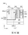
參照第1圖及第5A圖至第5D圖,方法100包括方塊108,在方塊108中,形成溝槽(例如:溝槽260a、260b及/或260c)以曝露源極/汲極特徵214。第5A圖描繪了工作件200的局部俯視圖,而第5B圖及第5C圖分別顯示了沿著第5A圖所示之線段B-B’及線段C-C’截取的工作件200的局部截面圖,並且第5D圖顯示了溝槽260a及260b的放大俯視圖。1 and 5A-5D,
在此操作中,為了形成溝槽260a或260b,使用了微影製程與蝕刻製程(例如:乾式蝕刻、濕式蝕刻及/或反應式離子蝕刻(reactive ion etching, RIE)))的組合來移除介電結構228的一些部分以及閘極隔離結構222的一些部分,以曝露源極/汲極特徵214。在一個範例性製程中,硬遮罩層及光阻被沉積在工作件200上方。光阻層接著被曝露於穿透光罩或從光罩反射的圖案化輻射,在曝後烤製程中進行烘烤,在顯影劑溶液中進行顯影,然後進行沖洗(rinse),進而形成圖案化光阻層。圖案化光阻層接著被用作蝕刻遮罩來蝕刻硬遮罩層,以形成圖案化硬遮罩層。圖案化硬遮罩層接著被用作蝕刻遮罩,以蝕刻介電結構228及閘極隔離結構222。蝕刻製程可為乾式蝕刻製程,包括使用氬(Ar)、含氟蝕刻劑(例如:SF6、NF3、CH2F2、CHF3、C4F8及/或C2F6)、含氧蝕刻劑、含氯蝕刻劑(例如:Cl2、CHCl3、CCl4及/或BCl3)、含溴蝕刻劑(例如:HBr及/或CHBr3)、含碘蝕刻劑、氧氣、氫氣、其他合適的氣體或其組合。In this operation, in order to form the
在本實施例中,沿著第5A圖所示之線段A-A’截取的工作件200的截面圖,與沿著線B-B’截取的工作件200的截面圖實質上相同。因此,在後續製程階段的描述中,省略了沿著線段A-A’截取之工作件200的截面圖。本技術領域具通常知識者應當理解,在那些製程階段中,沿著線段A-A’截取之工作件200的截面圖,實質上是為了沿著線段B-B’截取之工作件200的截面圖所描繪的那些截面圖的鏡像。儘管繪製了三個溝槽260a-260c,但應理解的是,工作件200可以包括位於各種相對位置之溝槽260a-260c的任意組合及數量。舉例來說,根據閘極隔離結構222的位置,工作件可以包括曝露源極/汲極特徵214c與214d的溝槽260a,以及曝露源極/汲極特徵214e與214f的溝槽260c。在本實施例中,溝槽260a、260b及260c包括錐形側壁。在一些其他實施例中,溝槽260a、260b及260c可包括實質上垂直的側壁。In the present embodiment, the cross-sectional view of the
在一些實施例中,溝槽260a-260c中的每一者,被形成為穿透到介電結構228之中及/或閘極隔離結構222之中。更具體地來說,在一些實施例中,從如第5A圖所示的俯視圖來看,閘極隔離結構222與溝槽260a彼此交叉。溝槽260a包括兩個第一部分260a-1,以及橫跨在兩個第一部分260a-1間的第二部分260a-2。兩個第一部分260a-1與第二部分260a-2在第5D圖中被虛線所分隔。兩個第一部分260a-1分別曝露了源極/汲極特徵214a及214b。在一些實施例中,第二部分260a-2並未與投影在沿著線段C-C’之截面圖上的金屬閘極結構210a存在重疊。從俯視圖來看,溝槽260a所具有的形狀,沿著其長度具有不均勻寬度。在一個實施例中,兩個第一部分260a-1沿著X方向跨越寬度W1並且沿著Z方向跨越深度D1。寬度W1可以實質上等於或小於溝槽260a、260b及260c之每一者兩側上的相鄰閘極間隔物212之間的距離。在一些實施例中,第二部分260a-2沿著X方向跨越寬度W3並且沿著Z方向跨越深度D3。寬度W1大於寬度W3。在一個實施例中,寬度W3對寬度W1的比值(即:W3/W1)處於約0.5至約0.95的範圍內。如果W3/W1太小,則將在溝槽260a中形成的源極/汲極接點(例如:將在下文中描述的源極/汲極接點218a) 與其下方的源極/汲極特徵(例如:源極/汲極特徵214a及214b)之間的接觸電阻可能會太大。如果W3/W1太大,則第二部分260a-2可能會太過靠近相鄰的金屬閘極結構210a-1及210a-2,使得金屬閘極結構210a-1及210a-2與源極/汲極接點218a之間的電性短路問題可能持續存在。在一些實施例中,深度D1大於深度D3。在一個實施例中,深度D3對深度D1的比值處於約0.3至約0.95的範圍內。In some embodiments, each of the
在一些實施例中,從如第5A圖所示的俯視圖來看,閘極隔離結構222的末端222e與溝槽260b具有重疊。類似於溝槽260a,溝槽260b包括兩個第一部分260b-1,以及橫跨在兩個第一部分260b-1之間的第二部分260b-2。兩個第一部分260b-1分別曝露源極/汲極特徵214c及214d。在一些實施例中,參照第5C圖,閘極間隔物212之側壁的一部分曝露於第二部分260b-2。在一些實施例中,第二部分260b-2並未與投影在沿著線段C-C’之截面圖上的金屬閘極結構210a重疊。從俯視圖來看,溝槽260b所具有的形狀,具有沿著其長度具有不均勻寬度。在一個實施例中,兩個第一部分260b-1沿著X方向跨越寬度W1並且沿著Z方向跨越深度D1。在一些實施例中,如第5C圖所示,第二部分260b-2沿著X方向跨越寬度W4並且沿著Z方向跨越深度D4。寬度W1大於寬度W4。在一個實施例中,寬度W4對寬度W1的比值(即:W4/W1)處於約0.7至約0.95的範圍內。如果W4/W1太小,則將在溝槽260b中形成的源極/汲極接點(例如:將在下文中描述的源極/汲極接點218b) 與其下方的源極/汲極特徵(例如:源極/汲極特徵214c及214d)之間的接觸電阻可能會太大。如果W4/W1太大,則第二部分260b-2可能會太過靠近相鄰的金屬閘極結構210a-1及210a-2,使得金屬閘極結構210a-1及210a-2與源極/汲極接點218b之間的電性短路可能持續存在。在一些實施例中,深度D1大於深度D4。在一個實施例中,深度D4對深度D1的比值處於約0.5至約0.95的範圍內。In some embodiments, from the top view as shown in FIG. 5A , the
在一些實施例中,寬度W4等於或大於寬度W3。在一個實施例中,寬度W3對寬度W4的比值(即:W3/W4)處於約0.7至約1的範圍內。如果W3/W4太小,則源極/汲極接點218a與其下方的源極/汲極特徵(例如:源極/汲極特徵214a及214b)之間的接觸電阻可能會太大,因而影響半導體結構的整體性能,或者,溝槽260b的第二部分260b-2可能會太靠近相鄰的金屬閘極結構210a-1及210a-2,使得金屬閘極結構210a-1及210a-2與源極/汲極接點218b之間的電性短路可能持續存在。如果W3/W4的比值太大,則源極/汲極接點218b與其下方的源極/汲極特徵(例如:源極/汲極特徵214c及214d)之間的接觸電阻可能太大,因而影響半導體結構的整體性能,或者,溝槽260a的第二部分260a-2可能會太靠近相鄰的金屬閘極結構210a-1及210a-2,使得金屬閘極結構210a-1及210a-2與源極/汲極接點218a之間的電性短路可能持續存在。在一些實施例中,深度D4等於或大於深度D3。在一個實施例中,深度D3對深度D4的比值處於約0.5至約1的範圍內。In some embodiments, width W4 is equal to or greater than width W3. In one embodiment, the ratio of width W3 to width W4 (ie, W3/W4) is in the range of about 0.7 to about 1. If W3/W4 is too small, the contact resistance between the source/
在一些實施例中,溝槽260c與閘極隔離結構222間隔開來。溝槽260c曝露源極/汲極特徵214e及214f。溝槽260c所具有的形狀,具有從俯視圖來看沿著其長度實質上均勻的寬度W2以及沿著Z方向的深度D2。寬度W2實質上等於寬度W1。深度D2實質上等於深度D1。In some embodiments,
參照第1圖及第6A圖至第6D圖,方法100包括方塊110,在方塊110中,分別於溝槽260a、260b及260c中形成源極/汲極接點218a、218b及218c。第6A圖描繪了工作件200的局部俯視圖,而第6B圖及第6C圖分別顯示了沿著第6A圖所示之線段B-B’及線段C-C’截取的工作件200的局部截面圖,並且第6D圖顯示了源極/汲極接點218a及218b的放大俯視圖。1 and 6A to 6D, the
在形成源極/汲極接點218a-218c之前,可在源極/汲極特徵214a-214f中的每一者上方形成矽化物層(未圖示)。在一些實施例中,矽化物層包括金屬矽化物,例如矽化鎳、矽化鈷、矽化鎢、矽化鉭、矽化鈦、矽化鉑、矽化鉺、矽化鈀、其他合適的矽化物或其組合。矽化物層可藉由沉積製程形成,例如CVD、ALD、PVD、其他合適的製程或其組合。舉例來說,可在源極/汲極特徵214a-214f上方沉積金屬層(例如:鎳)。接著,對工作件200進行退火,以使金屬層與源極/汲極特徵214a-214f的半導體材料產生反應。之後,移除未反應的金屬層,留下源極/汲極特徵214a-214f上方的矽化物層。替代性地,矽化物層可藉由任何合適的沉積方法直接形成在源極/汲極特徵214a-214f上方,例如CVD、ALD、PVD、其他合適的方法或其組合。Before forming the source/
源極/汲極接點218a、218b及218c的形成,可包括在溝槽260a、260b和260c中以及在金屬閘極結構210a和210b、閘極間隔物212和介電結構228的一些部分上方沉積導電層(未圖示)。導電層可包括任何合適的材料,例如W、Co、Ru、Cu、Ta、Ti、Al、Mo、其他合適的導電材料或其組合。導電層可藉由任何合適的方法進行沉積,例如CVD、PVD、ALD、電鍍、其他合適的方法或其組合。之後,方法100使用諸如CMP之合適的方法來平坦化工作件200的頂部表面,以在源極/汲極特徵214上方以及分別在溝槽260a、260b及260c中形成源極/汲極接點218a、218b及218c,使得導電層(即:所形成的源極/汲極接點218a、218b及218c)的頂部表面與金屬閘極結構210a及210b的頂部表面實質上共平面。在一些實施例中,於沉積導電層之前,可在工作件200上方形成膠黏層(glue layer)(未圖示)以部分地填充溝槽260a-260c。膠黏層可包括TiN、TaN等。The formation of the source/
源極/汲極接點218a-218c分別遵循溝槽260a- 260c的形狀。也就是說,源極/汲極接點218a、218b及218c的尺寸(例如:寬度、深度)實質上分別與溝槽260a、260b及260c相同。舉例來說,源極/汲極接點218a及218b的第一部分218a-1及218b-1具有深度D1,源極/汲極接點218a的第二部分218a-2具有深度D3,並且源極/汲極接點218b的第二部分218b-2具有深度D4。在一些實施例中,源極/汲極接點218a及218b的第一部分218a-1及218b-1具有寬度W1,源極/汲極接點218a的第二部分218a-2具有寬度W3,並且源極/汲極接點218b的第二部分218b-2具有寬度W4。源極/汲極接點218c具有實質上相同的寬度(即:深度W2)以及實質上相同的深度(即:深度D2)。The source/
此外,源極/汲極接點218a包括分別位於源極/汲極特徵214a及214b正上方並且電性耦接至源極/汲極特徵214a及214b的兩個第一部分218a-1,以及在兩個第一部分218a-1之間延伸的第二部分218a-2。在一些實施例中,從俯視圖來看,源極/汲極接點218a的第二部分218a-2包括向內彎曲的兩個邊緣220a(如第6D圖所示)。參照第6C圖,第二部分218a-2並未與投影在沿著線段C-C’之截面圖上的金屬閘極結構210a重疊。在一些實施例中,第二部分218a-2嵌入於閘極隔離結構222中。In addition, the source/
源極/汲極接點218b包括分別位於源極/汲極特徵214c及214d正上方並且電性耦接至源極/汲極特徵214c及214d的兩個第一部分218b-1,以及在兩個第一部分218b-1之間延伸的第二部分218b-2。在如第6D圖所示的實施例中,源極/汲極接點218b的第二部分218b-2包括向內彎曲的第一邊緣220b-1。源極/汲極接點218b之第二部分218b-2的與第一邊緣220b-1相對的第二邊緣220b-2,沿著Y方向與源極/汲極接點218b之第一部分218b-1的邊緣220b-3對準。換句話說,從俯視圖來看,源極/汲極接點218b的第一部分218b-1與第二部分218b-2共享沿著Y方向延伸的一個連續邊緣,並且此連續邊緣實質上是筆直的。換句話說,第二邊緣220b-2與邊緣220b-3之間並未沿著Y方向存在明顯的偏移。源極/汲極接點218b之第二部分218b-2的第一邊緣220b-1與金屬閘極結構210a之間的距離,小於源極/汲極接點218b之第二部分218b-2的第二邊緣220b-2與金屬閘極結構210a之間的距離。The source/
在一些實施例中,參照第6C圖,閘極隔離結構222的邊界223,位於源極/汲極接點218b之第二部分218b-2的正下方。第二部分218b-2的底部表面與閘極隔離結構222及介電結構228兩者直接接觸。在一個實施例中,介電結構228的一部分夾設於第二部分218b-2與閘極間隔物212之間。在一些實施例中,第二部分218b-2與閘極隔離結構222的側壁直接接觸。在一些實施例中,源極/汲極接點218b並未與投影在沿著線段C-C’之截面圖上的金屬閘極結構210a重疊。由環繞第二部分218b-2之點狀線所圍繞的區域219,代表即使在溝槽260b的形成期間存在諸如蝕刻變化、覆蓋偏移等,亦可在其中形成源極/汲極接點218b的區域。在一些實施例中,蝕刻閘極間隔物212的蝕刻速率,低於閘極隔離結構222的蝕刻速率。因此,在溝槽260b的形成期間,閘極隔離結構222被蝕刻得比閘極間隔物212還要多。因為第二部分218b-2所具有的寬度(例如:寬度W4)小於兩個第一部分218b-1的寬度,因此從第二部分218b-2到投影之金屬閘極結構210a的距離增加。因此,即使在溝槽260b的形成期間存在製造變動,因為距離的增加,因此第二部分218b-2與金屬閘極結構210a-1/210a-2的末端直接接觸的可能性得以降低。因此,可以避免金屬閘極結構210a與第二部分218b-2之間的電性短路。出於類似的原因,從源極/汲極接點218a的第二部分218a-2到投影之金屬閘極結構210a的距離得以增加,這亦消除了金屬閘極結構210a與第二部分218a-2之間的電性短路。In some embodiments, referring to FIG. 6C , the
回頭參照第1圖,方法100包括方塊112,在方塊112中,執行進一步的製程以完成工作件200的製造。這些進一步的製程以可以包括在工作件200上方形成多層互連(multi-layer interconnect, MLI)結構(未圖示)。在一些實施例中,MLI結構可包括複數金屬間介電(intermetal dielectric, IMD)層以及每個IMD層中的複數金屬線或接觸通孔。在一些實施例中,IMD層與介電結構228可以共享相似的成分。每個IMD層中的金屬線與接觸通孔可以由金屬形成,例如鋁、鎢、釕或銅。在一些實施例中,金屬線及接觸通孔可以由阻障層進行襯墊(line),以使金屬線及接觸通孔與IMD層絕緣。Referring back to FIG. 1 ,
在本實施例中,閘極隔離結構222的形成,晚於金屬閘極結構210a及210b的形成。在一些其他實施例中,閘極隔離結構222的形成,可以是在虛擬閘極結構的形成之前或是之後。舉例來說,閘隔離結構222可被形成為將虛擬閘極結構分割為兩個部分,並且虛擬閘極結構的這兩個部分可以接著被兩個金屬閘極結構(例如:金屬閘極結構210a-1及210a-2)分別取代。In the present embodiment, the
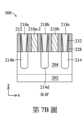
第7A圖描繪了第一個替代性的工作件300的局部俯視圖,而第7B圖及第7C圖分別顯示了沿著第7A圖所示之線段B-B’及線段C-C’截取的工作件300的局部截面圖。第7A圖至第7C圖中所示的工作件300,類似於參照第6A圖至第6D圖所述的工作件200。工作件300與工作件200之間的其中一個差異,包括在此替代性實施例中,工作件300包含介電阻障層232。更具體地來說,為了防止導電層的擴散,於形成溝槽260a-260c之後,介電阻障層232被形成在工作件300上方,並接著被回蝕刻(etch back)為僅覆蓋溝槽260a-260c的側壁並且曝露源極/汲極特徵214。源極/汲極接點218a、218b及218c可接著被形成在溝槽260a-260c中。也就是說,源極/汲極接點218a、218b及218c之每一者的側壁表面,被介電阻障層232所連續地襯墊。在一些實施例中,介電阻障層232可包括氮化矽或其他合適的材料。FIG. 7A depicts a partial top view of a first
第8A圖描繪了第二個替代性的工作件400的局部俯視圖,而第8B圖及第8C圖分別顯示了沿著第8A圖所示之線段B-B’及線段C-C’截取的工作件400的局部截面圖。第8A圖至第8C圖中所示的工作件400,類似於參照第6A圖至第6D圖所述的工作件200。工作件400與工作件200之間的其中一個差異,包括在此替代性實施例中,工作件400包括形成在金屬閘極結構210a及210b上方的自我對準覆帽(self-aligned cap, SAC)層252。在範例性製程中,可藉由移除(例如:蝕刻)金屬閘極結構210a及210b的頂部部分來形成SAC凹槽。接著,可以藉由CVD、PECVD或合適的沉積製程在包括SAC凹槽的工作件400上方沉積介電材料(未圖示)。介電材料可以包括氧化矽、氮化矽、碳化矽、碳氮化矽、氮氧化矽、碳氮氧化矽、氧化鋁、氮化鋁、氮氧化鋁、氧化鋯、氮化鋯、氧化鋯鋁、氧化鉿或是合適的介電材料。在沉積介電材料之後,可執行諸如CMP的平坦化製程,以移除介電結構228上方的多餘介電材料,進而在金屬閘極結構210a及210b正上方形成SAC層252。在形成SAC層252之後,接著執行微影製程與蝕刻製程以形成閘極隔離溝槽256。在本實施例中,由於金屬閘極結構210a及210b的掘入(recess),因此源極/汲極接點218a/218b/218c的頂部表面高於被掘入之金屬閘極結構210a及210b的頂部表面。在一些實施例中,源極/汲極接點218a、218b及218c的頂部表面與SAC層252的頂部表面共平面。FIG. 8A depicts a partial top view of a second
於所繪實施例中,SAC層252的側壁與至少一個閘極間隔物212直接接觸,並且SAC層252的底部表面與金屬閘極結構210a及210b的高k值介電層和金屬閘極電極的頂部表面直接接觸。在一些其他實施例中,SAC層252可以具有其他配置。舉例來說,SAC層凹槽可藉由掘入金屬閘極結構210a及210b的頂部部分以及掘入閘極間隔物212的頂部部分來形成,並且所獲得的SAC層252可被直接形成在被掘入的閘極間隔物212與金屬閘極結構210a及210b上。被掘入之閘極間隔物212的頂部表面可以高於金屬閘極結構210a及210b的頂部表面。In the illustrated embodiment, the sidewalls of the
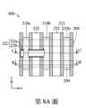
第9A圖描繪了第三個替代性的工作件500的局部俯視圖,而第9B圖顯示了沿著第8A圖所示之線段B-B’截取的工作件500的局部截面圖。第9A圖至第9B圖中所示的工作件500,類似於參照第6A圖至第6D圖所述的工作件200。工作件500與工作件200之間的其中一個差異,包括在此替代性實施例中,工作件500之源極/汲極接點的配置不同於工作件200之源極/汲極接點的配置。FIG. 9A depicts a partial top view of a third
在一些實施例中,工作件500包括形成在金屬閘極結構210a及210b上方的一或多個介電結構236及240,並且源極/汲極接點218a、218b及218c向上延伸至高於金屬閘極結構210a及210b的頂部表面,而且延伸穿過介電結構236。工作件500可進一步包括一或多個接觸通孔250以及閘極接觸通孔244,其中接觸通孔250嵌入於介電結構240中,位於源極/汲極接點218a、218b及/或218c上方,並電性耦接至源極/汲極接點218a、218b及/或218c,而閘極接觸通孔244位於金屬閘極結構210b上方並且電性耦接至金屬閘極結構210b。在一些實施例中,工作件500之沿著線段C-C’的截面圖可以類似於第6C圖中所示的工作件200,不同之處在於一或多個介電結構236及240被設置在閘極隔離結構222、介電結構228以及金屬閘極結構210a及210b上方,以及源極/汲極接點218a、218b及218c向上延伸進入/穿過介電結構236。In some embodiments, the
在一個範例性製程中,介電結構236被形成在介電結構228上方。對工作件500執行微影製程及蝕刻製程,以形成穿過介電結構236、介電結構228與閘極隔離結構222的溝槽260a- 260b,使得它們下方之對應的源極/汲極特徵214的上方表面被曝露。在後續的製程中,源極/汲極接點218a、218b及218c被形成在溝槽260a-260b中,類似於第6A圖至第6D圖中所描述的製程。進一步的製程可以包括在介電結構236上方形成介電結構240、在介電結構240中形成接觸通孔250、以及形成閘極接觸通孔244。In an exemplary process, the
第10圖描繪了第四個替代性的工作件600的局部截面圖。第四個替代性的工作件600的局部俯視圖類似於第6A圖,工作件600之沿著如第6A圖所示的線段B-B’截取的局部截面圖類似於第6B圖。第10圖顯示了工作件600之沿著第6A圖所示之線段C-C’截取的局部截面圖。在參照第6A圖至第6D圖所述的前述實施例中,為了形成閘極隔離溝槽256,閘極間隔物212及金屬閘極結構210a之被閘極隔離溝槽256所曝露的部分被實質上移除。在第10圖所示的第四替代性實施例中,於形成閘極隔離溝槽256時,執行選擇性蝕刻製程以擇性地移除金屬閘極結構210a之被閘極隔離溝槽256所曝露的的部分,而閘極間隔物212的曝露部分則是被輕微地蝕刻,使得在選擇性蝕刻之後,閘極間隔物212的一部分(亦稱為剩餘閘極間隔物212a)以及介電結構228的一部分(亦稱為剩餘介電結構228a)被閘極隔離溝槽256所曝露。在一些實施例中,剩餘閘極間隔物212a的側壁實質上未被蝕刻。可以在選擇性蝕刻製程中使用任何合適的方法,例如濕式蝕刻、乾式蝕刻或其組合,並且使用合適的蝕刻劑來蝕刻各種材料。FIG. 10 depicts a partial cross-sectional view of a fourth alternative workpiece 600. The partial top view of the fourth alternative workpiece 600 is similar to FIG. 6A, and the partial cross-sectional view of the workpiece 600 taken along the line segment B-B' shown in FIG. 6A is similar to FIG. 6B. FIG. 10 shows a partial cross-sectional view of the workpiece 600 taken along the line segment C-C' shown in FIG. 6A. In the aforementioned embodiments described with reference to FIGS. 6A to 6D, in order to form the
在本實施例中,形成在閘極隔離溝槽256中的閘極隔離結構222包括位於剩餘閘極間隔物212a正上方的第一部分222-1,以及位於兩個相鄰之剩餘閘極間隔物212a之間的第二部分222-2。在一些實施例中,閘極隔離結構222的第一部分222-1同樣位於剩餘介電結構228a的正上方。在一些實施例中,閘極隔離結構222的第二部分222-2延伸至隔離特徵208之中並且具有深度D7。閘極隔離結構222的第一部分222-1具有深度D8。深度D7可以大於金屬閘極結構210a及210b的深度D9。在一些實施例中,深度D7對深度D9的比值處於約1.05至約3的範圍內。如果此比值太小,則閘極隔離結構222可能無法將金屬閘極結構210a完全地分割為兩個隔離的部分。如果此比值太大,則閘極隔離結構222可能會延伸穿過隔離特徵208並且延伸到基板202之中,導致漏電流的增加。深度D7可以大於深度D8。在一些實施例中,深度D7對深度D8的比值處於約1.05至約5的範圍內。In the present embodiment, the
仍舊參照第10圖,源極/汲極接點218b之第二部分218b-2的上方部分,藉由閘極隔離結構222的第一部分222-1而與閘極隔離結構222的第二部分222-2分隔,並且源極/汲極接點218b之第二部分218b-2的下方部分,藉由剩餘介電結構228a及剩餘閘極間隔物212a而與閘極隔離結構222的第二部分222-2分隔。於所繪實施例中,源極/汲極接點218b之第二部分218b-2的底部表面,低於相鄰之剩餘閘極間隔物212a的頂部表面。在一些其他實施例中,源極/汲極接點218b之第二部分218b-2的底部表面,與相鄰之剩餘閘極間隔物212a的頂部表面共平面,或是高於相鄰之剩餘閘極間隔物212a的頂部表面。在一些實施例中,源極/汲極接點218a的第二部分218a-2位於剩餘介電結構228a的正上方。源極/汲極接點218a之第二部分218a-2的底部表面,可以在相鄰之剩餘閘極間隔物212a的頂部表面之上、之下或處於相同高度。Still referring to FIG. 10 , the upper portion of the
類似於參考照第6C圖所述的實施例,源極/汲極接點218b之第二部分218b-2周圍的區域219,代表即使在溝槽260b的形成期間存在諸如蝕刻變化、覆蓋偏移等,亦可在其中形成源極/汲極接點218b的區域。基於與前述相似的原因,第二部分218b-2與金屬閘極結構210a之末端直接接觸的可能性得以降低。此外,在一些實施例中,因為在形成溝槽260b時,蝕刻剩餘閘極間隔物212a的蝕刻速率低於蝕刻閘極隔離結構222的蝕刻速率,因此相鄰之剩餘閘極間隔物212a提供了更多的負擔(burden)以避免第二部分218b-2與金屬閘極結構210a的末端直接接觸。因此,可以避免金屬閘極結構210a與源極/汲極接點218b的第二部分218b-2之間的電性短路。出於類似的原因,同樣消除了金屬閘極結構210a與源極/汲極接點218a的第二部分218a-2之間的電性短路。Similar to the embodiment described with reference to FIG. 6C , the
第11A圖描繪了第五個替代性的工作件700的局部俯視圖,第11B圖顯示了沿著第11A圖所示之線段C-C’截取的工作件700的局部截面圖,第11C圖顯示了源極/汲極接點218d及218e的放大俯視圖。工作件700之沿著如第11A圖所示的線段B-B’截取的局部截面圖類似於第6B圖,為使說明簡化故而將其省略。工作件700類似於參照第6A圖至第6C圖所述的工作件200,並且工作件700與工作件200之間的其中一個差異,包括工作件700的閘極隔離結構具有與工作件200不同的配置。更具體地來說,工作件700包括被配置以將金屬閘極結構210a切割為兩個部分(即:第一部分210a-1及第二部分210a-2,亦稱為金屬閘極結構210a-1及210a-2,並且共同稱為金屬閘極結構210a)的第一閘極隔離結構222L,以及被配置以將金屬閘極結構210b切割為兩個部分210b-1及210b-2 (亦稱為金屬閘極結構210b-1及210b-2,並且共同稱為金屬閘極結構210b)的第二閘極隔離結構222R。第一閘極隔離結構222L與第二閘極隔離結構222R的形成類似於閘極隔離結構222的形成,不同之處在於兩個閘極隔離溝槽(未圖示)之每一者所橫跨的寬度小於溝槽256所橫跨的寬度,並且兩個閘極隔離溝槽中的每一者並未將閘極間隔物分割為物理性隔離的片段。也就是說,兩個閘極隔離溝槽之每一者的邊緣,同樣被兩個部分蝕刻的閘極間隔物212所侷限。如此一來,如第11A圖至第11C圖所示,閘極間隔物212之設置於隔離特徵208正上方並且與第一閘極隔離結構222L和第二閘極隔離結構222R直接接觸的部分(亦稱為剩餘閘極間隔物212b),其所具有之沿著X方向的寬度,小於閘極間隔物212之直接設置於金屬閘極結構210a及210b的側壁表面上的部分所具有之沿著X方向的寬度,並且剩餘閘極間隔物212b與第一閘極隔離結構222L或第二閘極隔離結構222R直接接觸。剩餘閘極間隔物212b所具有的高度,與閘極間隔物212之直接設置於金屬閘極結構210a及210b的側壁表面上的部分相同。FIG. 11A depicts a partial top view of a fifth
類似於第6A圖至第6D圖的源極/汲極接點218a,參照第11A圖至第11C圖,源極/汲極接點218d具有位於源極/汲極特徵214a及214b正上方的兩個第一部分218d-1,以及在兩個第一部分218d-1之間延伸的第二部分218d-2。第二部分218d-2介於第一閘極隔離結構222L與第二閘極隔離結構222R之間並且與它們兩個相鄰。在第11B圖所示的實施例中,第二部分218d-2嵌入於介電結構228中,其中此介電結構228位於兩個相鄰的剩餘閘極間隔物212b之間。更具體地來說,第二部分218d-2藉由剩餘閘極間隔物212b及介電結構228而與第一閘極隔離結構222L及第二閘極隔離結構222R間隔開來。Similar to the source/
類似於第6A圖至第6D圖的源極/汲極接點218b,源極/汲極接點218e具有位於源極/汲極特徵214c及214d正上方的兩個第一部分218e-1,以及在兩個第一部分218e-1之間延伸的第二部分218e-2。第二部分218e-2在一側與第二閘極隔離結構222R相鄰。在一些實施例中,第二部分218e-2嵌入於介電結構228中,此介電結構228介於一個相鄰的剩餘閘極間隔物212b與一個相鄰的閘極間隔物212之間。在一些實施例中,第二部分218e-2藉由剩餘閘極間隔物212b及介電結構228而與第二閘極隔離結構222R間隔開來。在一些實施例中,源極/汲極接點218e與相鄰的閘極間隔物212直接接觸。Similar to the source/
類似於參照第6C圖所述的實施例,區域219(顯示於第11B圖中)代表即使在溝槽260e(用於形成源極/汲極接點218e的溝槽,未圖示)的形成期間存在諸如蝕刻變化、覆蓋偏移等,亦可在其中形成源極/汲極接點218e的區域。在一些實施例中,蝕刻閘極間隔物212的蝕刻速率,低於蝕刻介電結構228的蝕刻速率。因此,在溝槽260e的形成期間,介電結構228被蝕刻得比閘極間隔物212還要多。基於與前述類似的原因,第二部分218e-2與金屬閘極結構210b之末端直接接觸的可能性得以降低。此外,在一些實施例中,因為在形成溝槽260e時,蝕刻剩餘閘極間隔物212b的蝕刻速率低於蝕刻第二閘極隔離結構222R的蝕刻速率,因此相鄰之剩餘閘極間隔物212b提供了更多的負擔以避免第二部分218e-2與金屬閘極結構210b的末端直接接觸。因此,可以避免金屬閘極結構210b與源極/汲極接點218e的第二部分218e-2之間的電性短路。出於類似的原因,同樣消除了金屬閘極結構210a及210b與源極/汲極接點218d的第二部分218d-2之間的電性短路。Similar to the embodiment described with reference to FIG. 6C , region 219 (shown in FIG. 11B ) represents a region in which source/
源極/汲極接點218d及218e分別具有與源極/汲極接點218a及218b相似的形狀。在一些實施例中,源極/汲極接點218d的第二部分218d-2具有沿著X方向的寬度W5以及沿著Z方向的深度D5。在一些實施例中,寬度W5小於寬度W1。在一些實施例中,寬度W5對寬度W1的比值(即:W5/W1)處於約0.5至約0.95的範圍內。如果W5/W1太小,則源極/汲極接點218d與其下方的源極/汲極特徵(例如:源極/汲極特徵214a及214b)之間的接觸電阻可能會太大。如果W5/W1太大,則第二部分260d-2可能會過於靠近相鄰的金屬閘極結構210a及210b,使得金屬閘極結構210a及210b與源極/汲極接點218d之間的電性短路可能持續存在。在一些實施例中,深度D5小於深度D1。在一些實施例中,深度D5對深度D1的比值處於約0.3至約0.95的範圍內。Source/
在一些實施例中,源極/汲極接點218e的第二部分218e-2具有沿著X方向的寬度W6以及沿著Z方向的深度D6。在一些實施例中,寬度W6小於寬度W1。在一些實施例中,寬度W6對寬度W1的比值(即:W6/W1)處於約0.5至約0.95的範圍內,或者是處於約0.7至約0.95的範圍內。如果W6/W1太小,則源極/汲極接點218e與其下方的源極/汲極特徵(例如:源極/汲極特徵214c及214d)之間的接觸電阻可能會太大。如果W6/W1太大,則第二部分260e-2可能會過於靠近相鄰的金屬閘極結構210b,使得金屬閘極結構210b與源極/汲極接點218e之間的電性短路可能持續存在。在一些實施例中,深度D6小於深度D1。在一個實施例中,深度D6對深度D1的比值處於約0.5至約0.95的範圍內。In some embodiments, the
在一些實施例中,寬度W6等於或大於寬度W5。在一些實施例中,寬度W5對寬度W6的比值(即:W5/W6)處於約0.7至約1的範圍內。如果W5/W6太小,則源極/汲極接點218d與其下方的源極/汲極特徵(例如:源極/汲極特徵214a及214b)之間的接觸電阻可能會太大,因而影響半導體結構的整體性能,或者,第二部分218e-2可能會太靠近相鄰的金屬閘極結構210b,使得金屬閘極結構210b與源極/汲極接點218e之間的電性短路可能持續存在。如果W5/W6太大,則源極/汲極接點218e與其下方的源極/汲極特徵(例如:源極/汲極特徵214c及214d)之間的接觸電阻可能會太大,因而影響半導體結構的整體性能,或者,第二部分218d-2可能會太靠近相鄰的金屬閘極結構210a及210b,使得金屬閘極結構210a及210b與源極/汲極接點218d之間的電性短路可能持續存在。在一些實施例中,深度D6等於或大於深度D5。在一個實施例中,深度D5對深度D6的比值處於約0.5至約1的範圍內。In some embodiments, width W6 is equal to or greater than width W5. In some embodiments, a ratio of width W5 to width W6 (i.e., W5/W6) is in a range of about 0.7 to about 1. If W5/W6 is too small, the contact resistance between source/
第12A圖描繪了第六個替代性的工作件800的局部俯視圖,第12B圖顯示了沿著第12A圖所示之線段C-C’截取的工作件800的局部截面圖。工作件800之沿著如第12A圖所示的線段B-B’截取的局部截面圖類似於第8B圖。工作件800與工作件700之間的其中一個差異,包括在此替代性實施例中,工作件800包括形成在金屬閘極結構210a及210b上方的SAC層252’。 SAC層252’可具有與第8A圖至第8C圖中所述之SAC層252相同的材料,並且以類似的方法形成。在一些實施例中,源極/汲極接點218d、218e及218c的頂部表面,高於金屬閘極結構210的頂部表面。FIG. 12A depicts a partial top view of a sixth
在參照第6A圖至第12A圖所述的前述實施例中,源極/汲極接點被配置為沿著其長度方向具有不均勻的寬度,並且顯示了源極/汲極接點的範例性俯視圖。在一些替代性實施例中,從俯視圖來看,源極/汲極接點(例如:源極/汲極接點218a及218b)具有不同的形狀。第13A圖描繪了第七個替代性的工作件900的局部俯視圖。第13B圖顯示了源極/汲極接點218a及218b的放大俯視圖。工作件900與工作件200之間的其中一個差異,包括在此替代性實施例中,從俯視圖來看,源極/汲極接點218a之第二部分218a-2的兩個邊緣220a-1以及源極/汲極接點218b之第二部分218b-2的第一邊緣220b-1實質上是筆直的,並且分別從第一部分218a-1及218b-1的邊緣220a-3及220b-4凹陷。換句話說,從俯視圖來看,源極/汲極接點218a的輪廓類似於啞鈴狀。源極/汲極接點218a及218b的尺寸(例如:寬度、深度),可以與先前所描述的相同。In the aforementioned embodiments described with reference to FIGS. 6A to 12A, the source/drain contacts are configured to have non-uniform widths along their lengths, and exemplary top views of the source/drain contacts are shown. In some alternative embodiments, the source/drain contacts (e.g., source/
半導體結構及其製造方法之實施例的各種組合,均包含在本揭露的範圍內。舉例來說,工作件可以包括SAC層252以及介電阻障層232。在其他範例中,源極/汲極接點218a、218b、218c、218d及/或218e延伸至高於金屬閘極結構210a及210b的頂部表面,並且具有第13A圖至第13B圖中所示的形狀。源極/汲極接點218a、218b、218c、218d及/或218e可以相對於彼此以任何數量及任何位置設置。Various combinations of embodiments of semiconductor structures and methods of making the same are within the scope of the present disclosure. For example, the workpiece may include a
儘管並非旨於進行限制,但本揭露一或多個實施例為半導體結構及其形成方法提供了諸多益處。舉例來說,其中一個優點是本揭露減少/避免了源極/汲極接點與相鄰金屬閘極結構之間的電性短路,同時不會犧牲源極/汲極接點與其下方的源極/汲極特徵之間的相對較低的接觸電阻。本揭露與各種半導體製造製程相容,並且與各種半導體結構(例如:具有SAC層及/或介電阻障層的半導體結構)相容。半導體結構可包括平面電晶體或是多重閘極裝置,例如FinFET、GAA、奈米片、叉片或CFET。Although not intended to be limiting, one or more embodiments of the present disclosure provide numerous benefits to semiconductor structures and methods of forming the same. For example, one advantage is that the present disclosure reduces/avoids electrical shorts between source/drain contacts and adjacent metal gate structures without sacrificing relatively low contact resistance between the source/drain contacts and the source/drain features thereunder. The present disclosure is compatible with a variety of semiconductor manufacturing processes and with a variety of semiconductor structures (e.g., semiconductor structures having SAC layers and/or dielectric barriers). The semiconductor structure may include a planar transistor or a multi-gate device, such as a FinFET, GAA, nanosheet, fork sheet, or CFET.
本揭露提供許多不同的實施例。半導體結構及其製造方法揭露於本文中。在一個範例性態樣中,本揭露直指一種半導體結構。上述半導體結構包括位於基板上方的源極/汲極特徵、沿著第一方向縱向延伸並且相鄰於源極/汲極特徵的金屬閘極結構、以及沿著實質上垂直於第一方向之第二方向縱向延伸的閘極隔離結構。閘極隔離結構將金屬閘極結構分割為兩個被隔離的部分。上述半導體結構更包括源極/汲極接點,源極/汲極接點電性耦接至源極/汲極特徵,並且包括位於源極/汲極特徵正上方的第一部分,以及沿著第一方向自第一部分延伸的第二部分。第一部分具有沿著第二方向的第一寬度,並且第二部分具有沿著第二方向的第二寬度。第一寬度大於第二寬度。The present disclosure provides many different embodiments. Semiconductor structures and methods for manufacturing the same are disclosed herein. In an exemplary embodiment, the present disclosure is directed to a semiconductor structure. The semiconductor structure includes a source/drain feature located above a substrate, a metal gate structure extending longitudinally along a first direction and adjacent to the source/drain feature, and a gate isolation structure extending longitudinally along a second direction substantially perpendicular to the first direction. The gate isolation structure divides the metal gate structure into two isolated portions. The semiconductor structure further includes a source/drain contact electrically coupled to the source/drain feature and includes a first portion directly above the source/drain feature and a second portion extending from the first portion along a first direction. The first portion has a first width along a second direction, and the second portion has a second width along the second direction. The first width is greater than the second width.
在一些實施例中,源極/汲極接點的第二部分包括在俯視圖中向內彎曲的兩個邊緣。在一些實施例中,於截面圖中,閘極隔離結構的邊界位於源極/汲極接點之第二部分的正下方。In some embodiments, the second portion of the source/drain contact includes two edges that are bent inward in a top view. In some embodiments, in a cross-sectional view, a boundary of the gate isolation structure is located directly below the second portion of the source/drain contact.
在一些實施例中,源極/汲極接點的第一部分具有第一深度,而源極/汲極接點的第二部分具有小於第一深度的第二深度。In some embodiments, a first portion of the source/drain contact has a first depth and a second portion of the source/drain contact has a second depth that is less than the first depth.
在一些實施例中,上述半導體結構更包括位於基板上方以及閘極隔離結構下方的隔離特徵,以及沿著第一方向縱向延伸的複數閘極間隔物。複數閘極間隔物包括位於金屬閘極結構之複數側壁上的第一部分,以及設置於隔離特徵正上方的第二部分。複數閘極間隔物的第二部分位於閘極隔離結構之第一部分的正下方。In some embodiments, the semiconductor structure further includes an isolation feature located above the substrate and below the gate isolation structure, and a plurality of gate spacers extending longitudinally along a first direction. The plurality of gate spacers include a first portion located on a plurality of sidewalls of the metal gate structure, and a second portion disposed directly above the isolation feature. The second portion of the plurality of gate spacers is located directly below the first portion of the gate isolation structure.
在一些實施例中,閘極隔離結構更包括相鄰於複數閘極間隔物之第二部分的一第二部分。閘極隔離結構的第二部分延伸至隔離特徵之中,並且閘極隔離結構之第二部分所具有的底部表面,低於閘極隔離結構之第一部分的底部表面。In some embodiments, the gate isolation structure further includes a second portion adjacent to the second portion of the plurality of gate spacers. The second portion of the gate isolation structure extends into the isolation feature, and the second portion of the gate isolation structure has a bottom surface that is lower than a bottom surface of the first portion of the gate isolation structure.
在一些實施例中,源極/汲極接點的頂部表面高於金屬閘極結構的頂部表面。In some embodiments, the top surface of the source/drain contacts is higher than the top surface of the metal gate structure.
在一些實施例中,上述源極/汲極特徵為第一源極/汲極特徵且上述源極/汲極接點為第一源極/汲極接點。上述半導體結構更包括第二源極/汲極特徵,使得金屬閘極結構被設置於第一源極/汲極特徵與第二源極/汲極特徵之間。在一些實施例中,上述半導體結構更包括第二源極/汲極接點,電性耦接至第二源極/汲極特徵,並且具有位於第二源極/汲極特徵正上方的第三部分,以及沿著第一方向自第三部分延伸的第四部分。第三部分具有第三寬度,而第四部分具有小於第三寬度的第四寬度。In some embodiments, the source/drain feature is a first source/drain feature and the source/drain contact is a first source/drain contact. The semiconductor structure further includes a second source/drain feature, such that the metal gate structure is disposed between the first source/drain feature and the second source/drain feature. In some embodiments, the semiconductor structure further includes a second source/drain contact electrically coupled to the second source/drain feature, and having a third portion directly above the second source/drain feature, and a fourth portion extending from the third portion along a first direction. The third portion has a third width, and the fourth portion has a fourth width that is less than the third width.
在一些實施例中,第二源極/汲極接點的第四部分包括在俯視圖中向內彎曲的第一邊緣,以及與第一邊緣相對並且與第三部分之邊緣對準的第二邊緣。In some embodiments, the fourth portion of the second source/drain contact includes a first edge that is bent inward in a top view, and a second edge opposite to the first edge and aligned with the edge of the third portion.
在一些實施例中,第二源極/汲極接點之第四部分所具有的深度,小於第二源極/汲極接點之第三部分的深度,並且大於第一源極/汲極接點之第二部分的深度。In some embodiments, the fourth portion of the second source/drain contact has a depth that is less than a depth of the third portion of the second source/drain contact and greater than a depth of the second portion of the first source/drain contact.
在另一個範例性態樣中,本揭露直指一種半導體結構。上述半導體結構包括位於基板上方的第一源極/汲極特徵與第二源極/汲極特徵、沿著第一方向在基板上方縱向延伸,並且分別相鄰於第一源極/汲極特徵與第二源極/汲極特徵的第一金屬閘極結構與第二金屬閘極結構、以及沿著實質上垂直於第一方向之第二方向縱向延伸的閘極隔離結構。第一金屬閘極結構與第二金屬閘極結構被閘極隔離結構所隔離。上述半導體結構更包括源極/汲極接點,源極/汲極接點包含位於第一源極/汲極特徵與第二源極/汲極特徵正上方的兩個第一部分,以及連接兩個第一部分的第二部分。第二部分相鄰於閘極隔離結構,並且兩個第一部分及第二部分具有不同的寬度。In another exemplary aspect, the present disclosure is directed to a semiconductor structure. The semiconductor structure includes a first source/drain feature and a second source/drain feature located above a substrate, a first metal gate structure and a second metal gate structure extending longitudinally along a first direction above the substrate and adjacent to the first source/drain feature and the second source/drain feature, respectively, and a gate isolation structure extending longitudinally along a second direction substantially perpendicular to the first direction. The first metal gate structure and the second metal gate structure are isolated by the gate isolation structure. The semiconductor structure further includes a source/drain contact, the source/drain contact includes two first parts located directly above the first source/drain feature and the second source/drain feature, and a second part connecting the two first parts. The second part is adjacent to the gate isolation structure, and the two first parts and the second part have different widths.
在一些實施例中,源極/汲極接點的第二部分嵌入於閘極隔離結構中。In some embodiments, a second portion of the source/drain contact is embedded in the gate isolation structure.
在一些實施例中,源極/汲極接點的第二部分位於閘極隔離結構之一部分的正上方,並且與閘極隔離結構的一側壁直接接觸。In some embodiments, the second portion of the source/drain contact is located directly above a portion of the gate isolation structure and directly contacts a sidewall of the gate isolation structure.
在一些實施例中,上述半導體結構更包括設置於第一源極/汲極特徵與第二源極/汲極特徵之間的隔離特徵,以及複數閘極間隔物。複數閘極間隔物具有位於第一金屬閘極結構與第二金屬閘極結構之複數側壁上的第一部分,以及設置於隔離特徵正上方的第二部分。源極/汲極接點的第二部分藉由複數閘極間隔物的第二部分與閘極隔離結構間隔開來。In some embodiments, the semiconductor structure further includes an isolation feature disposed between the first source/drain feature and the second source/drain feature, and a plurality of gate spacers. The plurality of gate spacers have a first portion located on a plurality of sidewalls of the first metal gate structure and the second metal gate structure, and a second portion disposed directly above the isolation feature. The second portion of the source/drain contact is separated from the gate isolation structure by the second portion of the plurality of gate spacers.
在一些實施例中,上述半導體結構更包括相鄰於閘極間隔物的介電層,其中源極/汲極接點嵌入於介電層中。在一些實施例中,於俯視圖中,源極/汲極特徵的輪廓近似於啞鈴狀。In some embodiments, the semiconductor structure further includes a dielectric layer adjacent to the gate spacer, wherein the source/drain contacts are embedded in the dielectric layer. In some embodiments, in a top view, the profile of the source/drain features is similar to a dumb bell.
在又一個範例性態樣中,本揭露直指一種半導體結構。上述半導體結構包括基板,以及位於基板上方並且彼此平行的第一主動區與第二主動區。第一主動區包括第一源極/汲極特徵,而第二主動區包括第二源極/汲極特徵。上述半導體結構更包括金屬閘極結構,金屬閘極結構沿著第一方向縱向延伸,位於第一主動區與第二主動區上方,並且相鄰於第一源極/汲極特徵與第二源極/汲極特徵。上述半導體結構更包括源極/汲極接點,源極/汲極接點包括分別位於第一源極/汲極特徵與第二源極/汲極特徵正上方的兩個第一部分,以及在兩個第一部分之間延伸的第二部分。兩個第一部分具有沿著實質上垂直於第一方向之第二方向的第一寬度,並且第二部分具有沿著第二方向的第二寬度。第一寬度大於第二寬度。In another exemplary embodiment, the present disclosure is directed to a semiconductor structure. The semiconductor structure includes a substrate, and a first active region and a second active region located above the substrate and parallel to each other. The first active region includes a first source/drain feature, and the second active region includes a second source/drain feature. The semiconductor structure further includes a metal gate structure, which extends longitudinally along a first direction, is located above the first active region and the second active region, and is adjacent to the first source/drain feature and the second source/drain feature. The semiconductor structure further includes a source/drain contact, the source/drain contact includes two first portions located directly above the first source/drain feature and the second source/drain feature, and a second portion extending between the two first portions. The two first portions have a first width along a second direction substantially perpendicular to the first direction, and the second portion has a second width along the second direction. The first width is greater than the second width.
在一些實施例中,上述半導體結構更包括位於金屬閘極結構之複數側壁上的複數閘極間隔物,以及沿著第二方向縱向延伸並且介於第一主動區與第二主動區之間的閘極隔離結構。閘極隔離結構將金屬閘極結構分割為兩個被隔離的部分,並且包括不同於閘極間隔物的介電材料。In some embodiments, the semiconductor structure further includes a plurality of gate spacers located on a plurality of sidewalls of the metal gate structure, and a gate isolation structure extending longitudinally along the second direction and between the first active region and the second active region. The gate isolation structure divides the metal gate structure into two isolated parts and includes a dielectric material different from that of the gate spacers.
在一些實施例中,閘極隔離結構包括外部層以及嵌入於外部層中的內部層。In some embodiments, the gate isolation structure includes an outer layer and an inner layer embedded in the outer layer.
在一些實施例中,上述半導體結構更包括沿著第二方向縱向延伸並且介於第一主動區與第二主動區之間的第一閘極隔離結構與第二閘極隔離結構。第一閘極隔離結構將金屬閘極結構分割為兩個被隔離的部分,並且源極/汲極接點的第二部分介於第一閘極隔離結構與第二閘極隔離結構之間。In some embodiments, the semiconductor structure further includes a first gate isolation structure and a second gate isolation structure extending longitudinally along the second direction and between the first active region and the second active region. The first gate isolation structure divides the metal gate structure into two isolated parts, and the second part of the source/drain contact is between the first gate isolation structure and the second gate isolation structure.
前述內文概述多項實施例之特徵,如此可使於本技術領域中具有通常知識者更佳地瞭解本揭露之態樣。本技術領域中具有通常知識者應當理解他們可輕易地以本揭露為基礎設計或修改其他製程及結構,以完成相同之目的及/或達到與本文介紹之實施例或範例相同之優點。本技術領域中具有通常知識者亦需理解,這些等效結構並未脫離本揭露之精神及範圍,且在不脫離本揭露之精神及範圍之情況下,可對本揭露進行各種改變、置換以及變更。The above text summarizes the features of various embodiments so that those with ordinary knowledge in the art can better understand the aspects of the present disclosure. Those with ordinary knowledge in the art should understand that they can easily design or modify other processes and structures based on the present disclosure to accomplish the same purpose and/or achieve the same advantages as the embodiments or examples introduced herein. Those with ordinary knowledge in the art should also understand that these equivalent structures do not deviate from the spirit and scope of the present disclosure, and that various changes, substitutions, and modifications can be made to the present disclosure without departing from the spirit and scope of the present disclosure.
100:方法 102-112:方塊 200:工作件 202:基板 204:主動區 204c:通道區域 204sd:源極/汲極區域 208:隔離特徵 210a:金屬閘極結構 210a-1:第一部分/金屬閘極結構 210a-2:第二部分/金屬閘極結構 210b:金屬閘極結構 210b-1:部分/金屬閘極結構 210b-2:部分/金屬閘極結構 212:閘極間隔物 212a:剩餘閘極間隔物 212b:剩餘閘極間隔物 214:源極/汲極特徵 214a-214f:源極/汲極特徵 218a:源極/汲極接點 218a-1:第一部分 218a-2:第二部分 218b:源極/汲極接點 218b-1:第一部分 218b-2:第二部分 218c:源極/汲極接點 218d:源極/汲極接點 218d-1:第一部分 218d-2:第二部分 218e:源極/汲極接點 218e-1:第一部分 218e-2:第二部分 219:區域 220a:邊緣 220a-1:邊緣 220a-3:邊緣 220b-1:第一邊緣 220b-2:第二邊緣 220b-3:邊緣 220b-4:邊緣 222:閘極隔離結構 222a:第一介電層 222b:第二介電層 222e:末端 222-1:第一部分 222-2:第二部分 222L:第一閘極隔離結構 222R:第二閘極隔離結構 223:邊界 228:介電結構 228a:剩餘介電結構 232:介電阻障層 236:介電結構 240:介電結構 244:閘極接觸通孔 250:接觸通孔 252:SAC層 252’:SAC層 256:閘極隔離溝槽 260a:溝槽 260a-1:第一部分 260a-2:第二部分 260b:溝槽 260b-1:第一部分 260b-2:第二部分 260c:溝槽 300-900:工作件 A-A’,B-B’,C-C’:線段 D1-D9:深度 W1-W6:寬度100: Method102-112: Block200: Workpiece202: Substrate204: Active region204c: Channel region204sd: Source/drain region208: Isolation feature210a: Metal gate structure210a-1: First portion/Metal gate structure210a-2: Second portion/Metal gate structure210b: Metal gate structure210b-1: Part/Metal gate structure210b-2: Part/Metal gate structure212: Gate spacer212a: Remaining gate spacer212b: Remaining gate spacer214: Source/drain features214a-214f: Source/drain features218a: Source/drain contacts218a-1: First section218a-2: Second section218b: Source/drain contacts218b-1: First section218b-2: Second section218c: Source/drain contacts218d: Source/drain contacts218d-1: First section218d-2: Second section218e: Source/drain contacts218e-1: First section218e-2: Second section219: Region220a: edge220a-1: edge220a-3: edge220b-1: first edge220b-2: second edge220b-3: edge220b-4: edge222: gate isolation structure222a: first dielectric layer222b: second dielectric layer222e: end222-1: first part222-2: second part222L: first gate isolation structure222R: second gate isolation structure223: boundary228: dielectric structure228a: remaining dielectric structure232: Dielectric barrier layer236: Dielectric structure240: Dielectric structure244: Gate contact via250: Contact via252: SAC layer252’: SAC layer256: Gate isolation trench260a: Trench260a-1: First part260a-2: Second part260b: Trench260b-1: First part260b-2: Second part260c: Trench300-900: WorkpieceA-A’, B-B’, C-C’: Line segmentD1-D9: DepthW1-W6: Width
本揭露之態樣自後續實施方式及圖式可以得到更佳的理解。須強調的是,依據產業之標準作法,各種特徵並未按比例繪製,並且僅用於說明之目的。事實上,各種特徵之尺寸可能任意增加或減少以使論述清晰易懂。 第1圖係根據本揭露一或多個態樣所示,用於形成半導體結構之方法的流程圖。 第2A圖、第3A圖、第4A圖、第5A圖及第6A圖係根據本揭露多種態樣所示,於第1圖之方法的多種製造階段期間之範例性工作件的局部俯視圖。 第2B圖、第3B圖、第4B圖、第5B圖及第6B圖係根據本揭露多種態樣所示,於第1圖之方法的多種製造階段期間,工作件分別沿著第2A圖、第3A圖、第4A圖、第5A圖及第6A圖之線段B-B’的局部截面圖。 第2C圖、第3C圖、第4C圖、第5C圖及第6C圖係根據本揭露多種態樣所示,於第1圖之方法的多種製造階段期間,工作件分別沿著第2A圖、第3A圖、第4A圖、第5A圖及第6A圖之線段C-C’的局部截面圖。 第5D圖及第6D圖係根據本揭露多種態樣所示,於第1圖之方法的多種製造階段期間,工作件之一部分的放大局部俯視圖。 第7A圖係根據本揭露多種態樣所示之第一替代性工作件的局部俯視圖。 第7B圖及第7C圖係根據本揭露多種態樣所示,分別沿著第7A圖之線段B-B’及C-C’截取的第一替代性工作件的局部截面圖。 第8A圖係根據本揭露多種態樣所示之第二替代性工作件的局部俯視圖。 第8B圖及第8C圖係根據本揭露多種態樣所示,分別沿著第8A圖之線段B-B’及C-C’截取的第二替代性工作件的局部截面圖。 第9A圖係根據本揭露多種態樣所示之第三替代性工作件的局部俯視圖。 第9B圖係根據本揭露多種態樣所示,沿著第9A圖之線段B-B’截取的第三替代性工作件的局部截面圖。 第10圖係根據本揭露多種態樣所示,沿著線段C-C’截取的第四替代性工作件的局部截面圖。 第11A圖係根據本揭露多種態樣所示之第五替代性工作件的局部俯視圖。 第11B圖係根據本揭露多種態樣所示,沿著第11A圖之線段C-C’截取的第五替代性工作件的局部截面圖。 第11C圖係根據本揭露多種態樣所示,第五替代性工作件之一部分的放大局部俯視圖。 第12A圖係根據本揭露多種態樣所示之第六替代性工作件的局部俯視圖。 第12B圖係根據本揭露多種態樣所示,沿著第12A圖之線段C-C’截取的第六替代性工作件的局部截面圖。 第13A圖係根據本揭露多種態樣所示之第七替代性工作件的局部俯視圖。 第13B圖係根據本揭露多種態樣所示,第七替代性工作件之一部分的放大局部俯視圖。The aspects of the present disclosure may be better understood from the following embodiments and drawings. It should be emphasized that, in accordance with standard industry practice, the various features are not drawn to scale and are used for illustrative purposes only. In fact, the sizes of the various features may be arbitrarily increased or decreased to make the discussion clear and understandable.FIG. 1 is a flow chart of a method for forming a semiconductor structure according to one or more aspects of the present disclosure.FIG. 2A, FIG. 3A, FIG. 4A, FIG. 5A and FIG. 6A are partial top views of exemplary workpieces during various manufacturing stages of the method of FIG. 1 according to various aspects of the present disclosure.Figures 2B, 3B, 4B, 5B and 6B are partial cross-sectional views of the workpiece along the line segments B-B’ of Figures 2A, 3A, 4A, 5A and 6A, respectively, during various manufacturing stages of the method of Figure 1 according to various aspects of the present disclosure.Figures 2C, 3C, 4C, 5C and 6C are partial cross-sectional views of the workpiece along the line segments C-C’ of Figures 2A, 3A, 4A, 5A and 6A, respectively, during various manufacturing stages of the method of Figure 1 according to various aspects of the present disclosure.Figures 5D and 6D are enlarged partial top views of a portion of the workpiece during various manufacturing stages of the method of Figure 1 according to various aspects of the present disclosure.FIG. 7A is a partial top view of a first alternative workpiece according to various aspects of the present disclosure.FIG. 7B and FIG. 7C are partial cross-sectional views of a first alternative workpiece taken along line segments B-B’ and C-C’ of FIG. 7A, respectively, according to various aspects of the present disclosure.FIG. 8A is a partial top view of a second alternative workpiece according to various aspects of the present disclosure.FIG. 8B and FIG. 8C are partial cross-sectional views of a second alternative workpiece taken along line segments B-B’ and C-C’ of FIG. 8A, respectively, according to various aspects of the present disclosure.FIG. 9A is a partial top view of a third alternative workpiece according to various aspects of the present disclosure.FIG. 9B is a partial cross-sectional view of a third alternative workpiece taken along line segment B-B’ of FIG. 9A, according to various aspects of the present disclosure.FIG. 10 is a partial cross-sectional view of a fourth alternative workpiece according to various aspects of the present disclosure, taken along line segment C-C'.FIG. 11A is a partial top view of a fifth alternative workpiece according to various aspects of the present disclosure.FIG. 11B is a partial cross-sectional view of a fifth alternative workpiece according to various aspects of the present disclosure, taken along line segment C-C' of FIG. 11A.FIG. 11C is an enlarged partial top view of a portion of the fifth alternative workpiece according to various aspects of the present disclosure.FIG. 12A is a partial top view of a sixth alternative workpiece according to various aspects of the present disclosure.FIG. 12B is a partial cross-sectional view of a sixth alternative workpiece according to various aspects of the present disclosure, taken along line segment C-C' of FIG. 12A.FIG. 13A is a partial top view of a seventh alternative workpiece according to various aspects of the present disclosure.Figure 13B is an enlarged partial top view of a portion of the seventh alternative workpiece according to various aspects of the present disclosure.
200:工作件200: Workpiece
204:主動區204: Active zone
210a-1:第一部分/金屬閘極結構210a-1: Part I/Metal Gate Structure
210a-2:第二部分/金屬閘極結構210a-2: Part II/Metal Gate Structure
210b:金屬閘極結構210b: Metal gate structure
212:閘極間隔物212: Gate spacer
218a,218b,218c:源極/汲極接點218a, 218b, 218c: Source/drain contacts
222:閘極隔離結構222: Gate isolation structure
222a:第一介電層222a: first dielectric layer
222b:第二介電層222b: Second dielectric layer
B-B’,C-C’:線段B-B’,C-C’: line segment
Claims (20)
Translated fromChineseApplications Claiming Priority (2)
| Application Number | Priority Date | Filing Date | Title |
|---|---|---|---|
| US18/335,380US20240421200A1 (en) | 2023-06-15 | 2023-06-15 | Source/Drain Contacts and Methods for Forming the Same |
| US18/335,380 | 2023-06-15 |
Publications (1)
| Publication Number | Publication Date |
|---|---|
| TW202501718Atrue TW202501718A (en) | 2025-01-01 |
Family
ID=93843758
Family Applications (1)
| Application Number | Title | Priority Date | Filing Date |
|---|---|---|---|
| TW112129480ATW202501718A (en) | 2023-06-15 | 2023-08-07 | Semiconductor structure |
Country Status (3)
| Country | Link |
|---|---|
| US (1) | US20240421200A1 (en) |
| CN (1) | CN222721871U (en) |
| TW (1) | TW202501718A (en) |
Families Citing this family (1)
| Publication number | Priority date | Publication date | Assignee | Title |
|---|---|---|---|---|
| US20240154014A1 (en)* | 2022-11-05 | 2024-05-09 | Taiwan Semiconductor Manufacturing Company, Ltd. | Semiconductor device and method for manufacturing thereof |
Family Cites Families (44)
| Publication number | Priority date | Publication date | Assignee | Title |
|---|---|---|---|---|
| KR0161399B1 (en)* | 1995-03-13 | 1998-12-01 | 김광호 | Nonvolatile Memory Device and Manufacturing Method |
| US5879998A (en)* | 1997-07-09 | 1999-03-09 | Advanced Micro Devices, Inc. | Adaptively controlled, self-aligned, short channel device and method for manufacturing same |
| KR100316709B1 (en)* | 1998-07-13 | 2001-12-12 | 윤종용 | Fabrication method of non-volatile memory device |
| US9716142B2 (en)* | 2015-10-12 | 2017-07-25 | International Business Machines Corporation | Stacked nanowires |
| TWI577010B (en)* | 2016-05-18 | 2017-04-01 | 杰力科技股份有限公司 | Power mosfet |
| US10872980B2 (en)* | 2017-04-25 | 2020-12-22 | Taiwan Semiconductor Manufacturing Co., Ltd. | Semiconductor device and manufacturing method thereof |
| KR102385567B1 (en)* | 2017-08-29 | 2022-04-12 | 삼성전자주식회사 | Semiconductor devices and method of manufacturing semiconductor devices |
| KR102528205B1 (en)* | 2018-06-26 | 2023-05-03 | 에스케이하이닉스 주식회사 | Cryogenic Semiconductor Device Having a Buried Channel Array Transistor |
| US11227918B2 (en)* | 2018-07-31 | 2022-01-18 | Taiwan Semiconductor Manufacturing Company, Ltd. | Melt anneal source and drain regions |
| US12266654B2 (en)* | 2018-07-31 | 2025-04-01 | Taiwan Semiconductor Manufacturing Company, Ltd. | FinFET devices and methods of forming the same |
| US10930564B2 (en)* | 2018-08-31 | 2021-02-23 | Taiwan Semiconductor Manufacturing Co., Ltd. | Metal gate structure cutting process |
| KR102697625B1 (en)* | 2019-01-16 | 2024-08-23 | 삼성전자주식회사 | Field separation layer and the same methoed |
| KR102655419B1 (en)* | 2019-05-14 | 2024-04-05 | 삼성전자주식회사 | Semiconductor devices |
| US11217680B2 (en)* | 2019-05-23 | 2022-01-04 | International Business Machines Corporation | Vertical field-effect transistor with T-shaped gate |
| KR102765096B1 (en)* | 2019-06-26 | 2025-02-06 | 삼성전자주식회사 | Semiconductor device and method for fabricating the same |
| US10985165B2 (en)* | 2019-08-19 | 2021-04-20 | Micron Technology, Inc. | Methods of forming microelectronic devices |
| KR102702992B1 (en)* | 2019-10-04 | 2024-09-04 | 삼성전자주식회사 | Integrated Circuit devices and manufacturing methods for the same |
| US11145727B2 (en)* | 2019-10-29 | 2021-10-12 | Nanya Technology Corporation | Semiconductor structure and method of forming the same |
| US11227794B2 (en)* | 2019-12-19 | 2022-01-18 | Taiwan Semiconductor Manufacturing Co., Ltd. | Method for making self-aligned barrier for metal vias In-Situ during a metal halide pre-clean and associated interconnect structure |
| KR20210092360A (en)* | 2020-01-15 | 2021-07-26 | 삼성전자주식회사 | Semiconductor device |
| DE102020119940A1 (en)* | 2020-03-31 | 2021-09-30 | Taiwan Semiconductor Manufacturing Co., Ltd. | MULTIPLE GATE TRANSISTOR STRUCTURE |
| US11316023B2 (en)* | 2020-06-15 | 2022-04-26 | Taiwan Semiconductor Manufacturing Co., Ltd. | Dumbbell shaped self-aligned capping layer over source/drain contacts and method thereof |
| US11664272B2 (en)* | 2020-09-29 | 2023-05-30 | Taiwan Semiconductor Manufacturing Co., Ltd. | Etch profile control of gate contact opening |
| US11664431B2 (en)* | 2021-01-08 | 2023-05-30 | Taiwan Semiconductor Manufacturing Company, Ltd. | Ring transistor structure |
| KR20220114143A (en)* | 2021-02-08 | 2022-08-17 | 삼성전자주식회사 | Semiconductor device |
| KR20220134835A (en)* | 2021-03-26 | 2022-10-06 | 삼성전자주식회사 | Semiconductor devices and method for manufacturing semiconductor devices |
| US12342594B2 (en)* | 2021-04-21 | 2025-06-24 | Changxin Memory Technologies, Inc. | Semiconductor structure and method for fabricating semiconductor structure |
| US12142686B2 (en)* | 2021-05-26 | 2024-11-12 | Globalfoundries U.S. Inc. | Field effect transistor |
| US11942372B2 (en)* | 2021-08-27 | 2024-03-26 | Taiwan Semiconductor Manufacturing Company, Ltd. | Dielectric protection layer in middle-of-line interconnect structure manufacturing method |
| US20240030289A1 (en)* | 2022-07-22 | 2024-01-25 | Changxin Memory Technologies, Inc. | Semiconductor structure and method for manufacturing same |
| US20240055476A1 (en)* | 2022-08-11 | 2024-02-15 | Taiwan Semiconductor Manufacturing Company, Ltd. | Isolation Structures in Semiconductor Devices |
| US20240079277A1 (en)* | 2022-09-07 | 2024-03-07 | Taiwan Semiconductor Manufacturing Company, Ltd. | Semiconductor device structure with gate stack and method for forming the same |
| US20240105787A1 (en)* | 2022-09-27 | 2024-03-28 | Taiwan Semiconductor Manufacturing Company, Ltd. | Semiconductor devices and methods of fabrication thereof |
| US20250079265A1 (en)* | 2022-10-11 | 2025-03-06 | Samsung Electronics Co., Ltd. | Semiconductor device |
| US20240170339A1 (en)* | 2022-11-23 | 2024-05-23 | Taiwan Semiconductor Manufacturing Company, Ltd. | Method of manufacturing a semiconductor device and a semiconductor device |
| CN118175847A (en)* | 2022-12-09 | 2024-06-11 | 长江存储科技有限责任公司 | Semiconductor structures, three-dimensional memories, storage systems and electronic devices |
| KR20240088076A (en)* | 2022-12-13 | 2024-06-20 | 삼성전자주식회사 | A semiconductor device |
| US20240266410A1 (en)* | 2023-02-02 | 2024-08-08 | Taiwan Semiconductor Manufacturing Company, Ltd. | Semiconductor structure and method for forming the same |
| US20240332408A1 (en)* | 2023-03-31 | 2024-10-03 | Taiwan Semiconductor Manufacturing Company, Ltd. | Isolation Structures |
| KR20240173069A (en)* | 2023-06-02 | 2024-12-10 | 삼성전자주식회사 | Semiconductor device |
| US20250006559A1 (en)* | 2023-06-29 | 2025-01-02 | Taiwan Semiconductor Manufacturing Company, Ltd. | Gate isolation structures and methods of forming the same |
| KR20250066611A (en)* | 2023-11-07 | 2025-05-14 | 삼성전자주식회사 | Semiconductor device |
| US20250159918A1 (en)* | 2023-11-09 | 2025-05-15 | Taiwan Semiconductor Manufacturing Company, Ltd. | Gate isolation features |
| US20250234578A1 (en)* | 2024-01-12 | 2025-07-17 | Taiwan Semiconductor Manufacturing Company, Ltd. | Semiconductor device with dielectric structure in channel region and manufacturing methods thereof |
- 2023
- 2023-06-15USUS18/335,380patent/US20240421200A1/enactivePending
- 2023-08-07TWTW112129480Apatent/TW202501718A/enunknown
- 2024
- 2024-06-03CNCN202421259428.3Upatent/CN222721871U/enactiveActive
Also Published As
| Publication number | Publication date |
|---|---|
| US20240421200A1 (en) | 2024-12-19 |
| CN222721871U (en) | 2025-04-04 |
Similar Documents
| Publication | Publication Date | Title |
|---|---|---|
| KR102261369B1 (en) | Metal gate structure cutting process | |
| KR20190136883A (en) | Structure and method for finfet device with contact over dielectric gate | |
| CN110875189A (en) | Method for forming semiconductor device | |
| TWI785777B (en) | Semiconductor device and method of forming the same | |
| CN106981516A (en) | Semiconductor device with a plurality of semiconductor chips | |
| KR102593872B1 (en) | Method of forming contact structures | |
| US11855082B2 (en) | Integrated circuits with FinFET gate structures | |
| CN110875252B (en) | Semiconductor device and method of manufacturing semiconductor device | |
| CN108574007A (en) | Semiconductor device and manufacturing method thereof | |
| US11387233B2 (en) | Semiconductor device structure and methods of forming the same | |
| TW202201495A (en) | Method of manufacturing the integrated circuit device | |
| KR20220113231A (en) | Hybrid semiconductor device | |
| TW202238996A (en) | Semiconductor device structure | |
| TW202013742A (en) | Semiconductor device and its manufacturing method | |
| US20240297236A1 (en) | Methods of reducing capacitance in field-effect transistors | |
| TWI814001B (en) | Semiconductor structure and method for forming the same | |
| CN222721871U (en) | Semiconductor structure | |
| US20240395866A1 (en) | Methods of forming epitaxial source/drain features in semiconductor devices | |
| TW202243032A (en) | Semiconductor structure and method of forming the same | |
| CN220021120U (en) | Semiconductor structure | |
| TW202015174A (en) | Method for forming semiconductor device | |
| US20230197802A1 (en) | Connection between gate and source/drain feature | |
| TW202245270A (en) | Semiconductor device structure | |
| CN115148604A (en) | Semiconductor device and method for manufacturing the same | |
| TWI878777B (en) | Semiconductor device and fabricating method thereof |