TW202422856A - Semiconductor device - Google Patents
Semiconductor deviceDownload PDFInfo
- Publication number
- TW202422856A TW202422856ATW113103392ATW113103392ATW202422856ATW 202422856 ATW202422856 ATW 202422856ATW 113103392 ATW113103392 ATW 113103392ATW 113103392 ATW113103392 ATW 113103392ATW 202422856 ATW202422856 ATW 202422856A
- Authority
- TW
- Taiwan
- Prior art keywords
- transistor
- oxide semiconductor
- potential
- insulating layer
- electrode
- Prior art date
Links
Images


Classifications
- H—ELECTRICITY
- H10—SEMICONDUCTOR DEVICES; ELECTRIC SOLID-STATE DEVICES NOT OTHERWISE PROVIDED FOR
- H10B—ELECTRONIC MEMORY DEVICES
- H10B41/00—Electrically erasable-and-programmable ROM [EEPROM] devices comprising floating gates
- H10B41/20—Electrically erasable-and-programmable ROM [EEPROM] devices comprising floating gates characterised by three-dimensional arrangements, e.g. with cells on different height levels
- H—ELECTRICITY
- H10—SEMICONDUCTOR DEVICES; ELECTRIC SOLID-STATE DEVICES NOT OTHERWISE PROVIDED FOR
- H10D—INORGANIC ELECTRIC SEMICONDUCTOR DEVICES
- H10D62/00—Semiconductor bodies, or regions thereof, of devices having potential barriers
- H10D62/10—Shapes, relative sizes or dispositions of the regions of the semiconductor bodies; Shapes of the semiconductor bodies
- G—PHYSICS
- G11—INFORMATION STORAGE
- G11C—STATIC STORES
- G11C11/00—Digital stores characterised by the use of particular electric or magnetic storage elements; Storage elements therefor
- G11C11/21—Digital stores characterised by the use of particular electric or magnetic storage elements; Storage elements therefor using electric elements
- G11C11/34—Digital stores characterised by the use of particular electric or magnetic storage elements; Storage elements therefor using electric elements using semiconductor devices
- G11C11/40—Digital stores characterised by the use of particular electric or magnetic storage elements; Storage elements therefor using electric elements using semiconductor devices using transistors
- G11C11/401—Digital stores characterised by the use of particular electric or magnetic storage elements; Storage elements therefor using electric elements using semiconductor devices using transistors forming cells needing refreshing or charge regeneration, i.e. dynamic cells
- G11C11/403—Digital stores characterised by the use of particular electric or magnetic storage elements; Storage elements therefor using electric elements using semiconductor devices using transistors forming cells needing refreshing or charge regeneration, i.e. dynamic cells with charge regeneration common to a multiplicity of memory cells, i.e. external refresh
- G11C11/405—Digital stores characterised by the use of particular electric or magnetic storage elements; Storage elements therefor using electric elements using semiconductor devices using transistors forming cells needing refreshing or charge regeneration, i.e. dynamic cells with charge regeneration common to a multiplicity of memory cells, i.e. external refresh with three charge-transfer gates, e.g. MOS transistors, per cell
- G—PHYSICS
- G11—INFORMATION STORAGE
- G11C—STATIC STORES
- G11C16/00—Erasable programmable read-only memories
- G11C16/02—Erasable programmable read-only memories electrically programmable
- G11C16/04—Erasable programmable read-only memories electrically programmable using variable threshold transistors, e.g. FAMOS
- G11C16/0408—Erasable programmable read-only memories electrically programmable using variable threshold transistors, e.g. FAMOS comprising cells containing floating gate transistors
- G11C16/0433—Erasable programmable read-only memories electrically programmable using variable threshold transistors, e.g. FAMOS comprising cells containing floating gate transistors comprising cells containing a single floating gate transistor and one or more separate select transistors
- H—ELECTRICITY
- H01—ELECTRIC ELEMENTS
- H01L—SEMICONDUCTOR DEVICES NOT COVERED BY CLASS H10
- H01L21/00—Processes or apparatus adapted for the manufacture or treatment of semiconductor or solid state devices or of parts thereof
- H01L21/02—Manufacture or treatment of semiconductor devices or of parts thereof
- H01L21/02104—Forming layers
- H01L21/02365—Forming inorganic semiconducting materials on a substrate
- H01L21/02656—Special treatments
- H01L21/02664—Aftertreatments
- H—ELECTRICITY
- H01—ELECTRIC ELEMENTS
- H01L—SEMICONDUCTOR DEVICES NOT COVERED BY CLASS H10
- H01L21/00—Processes or apparatus adapted for the manufacture or treatment of semiconductor or solid state devices or of parts thereof
- H01L21/02—Manufacture or treatment of semiconductor devices or of parts thereof
- H01L21/04—Manufacture or treatment of semiconductor devices or of parts thereof the devices having potential barriers, e.g. a PN junction, depletion layer or carrier concentration layer
- H01L21/34—Manufacture or treatment of semiconductor devices or of parts thereof the devices having potential barriers, e.g. a PN junction, depletion layer or carrier concentration layer the devices having semiconductor bodies not provided for in groups H01L21/18, H10D48/04 and H10D48/07, with or without impurities, e.g. doping materials
- H01L21/46—Treatment of semiconductor bodies using processes or apparatus not provided for in groups H01L21/428
- H—ELECTRICITY
- H10—SEMICONDUCTOR DEVICES; ELECTRIC SOLID-STATE DEVICES NOT OTHERWISE PROVIDED FOR
- H10B—ELECTRONIC MEMORY DEVICES
- H10B41/00—Electrically erasable-and-programmable ROM [EEPROM] devices comprising floating gates
- H10B41/10—Electrically erasable-and-programmable ROM [EEPROM] devices comprising floating gates characterised by the top-view layout
- H—ELECTRICITY
- H10—SEMICONDUCTOR DEVICES; ELECTRIC SOLID-STATE DEVICES NOT OTHERWISE PROVIDED FOR
- H10B—ELECTRONIC MEMORY DEVICES
- H10B41/00—Electrically erasable-and-programmable ROM [EEPROM] devices comprising floating gates
- H10B41/30—Electrically erasable-and-programmable ROM [EEPROM] devices comprising floating gates characterised by the memory core region
- H10B41/35—Electrically erasable-and-programmable ROM [EEPROM] devices comprising floating gates characterised by the memory core region with a cell select transistor, e.g. NAND
- H—ELECTRICITY
- H10—SEMICONDUCTOR DEVICES; ELECTRIC SOLID-STATE DEVICES NOT OTHERWISE PROVIDED FOR
- H10B—ELECTRONIC MEMORY DEVICES
- H10B41/00—Electrically erasable-and-programmable ROM [EEPROM] devices comprising floating gates
- H10B41/70—Electrically erasable-and-programmable ROM [EEPROM] devices comprising floating gates the floating gate being an electrode shared by two or more components
- H—ELECTRICITY
- H10—SEMICONDUCTOR DEVICES; ELECTRIC SOLID-STATE DEVICES NOT OTHERWISE PROVIDED FOR
- H10D—INORGANIC ELECTRIC SEMICONDUCTOR DEVICES
- H10D30/00—Field-effect transistors [FET]
- H10D30/60—Insulated-gate field-effect transistors [IGFET]
- H10D30/67—Thin-film transistors [TFT]
- H10D30/674—Thin-film transistors [TFT] characterised by the active materials
- H10D30/6755—Oxide semiconductors, e.g. zinc oxide, copper aluminium oxide or cadmium stannate
- H10D30/6756—Amorphous oxide semiconductors
- H—ELECTRICITY
- H10—SEMICONDUCTOR DEVICES; ELECTRIC SOLID-STATE DEVICES NOT OTHERWISE PROVIDED FOR
- H10D—INORGANIC ELECTRIC SEMICONDUCTOR DEVICES
- H10D84/00—Integrated devices formed in or on semiconductor substrates that comprise only semiconducting layers, e.g. on Si wafers or on GaAs-on-Si wafers
- H10D84/01—Manufacture or treatment
- H10D84/02—Manufacture or treatment characterised by using material-based technologies
- H10D84/08—Manufacture or treatment characterised by using material-based technologies using combinations of technologies, e.g. using both Si and SiC technologies or using both Si and Group III-V technologies
- H—ELECTRICITY
- H10—SEMICONDUCTOR DEVICES; ELECTRIC SOLID-STATE DEVICES NOT OTHERWISE PROVIDED FOR
- H10D—INORGANIC ELECTRIC SEMICONDUCTOR DEVICES
- H10D86/00—Integrated devices formed in or on insulating or conducting substrates, e.g. formed in silicon-on-insulator [SOI] substrates or on stainless steel or glass substrates
- H10D86/40—Integrated devices formed in or on insulating or conducting substrates, e.g. formed in silicon-on-insulator [SOI] substrates or on stainless steel or glass substrates characterised by multiple TFTs
- H10D86/421—Integrated devices formed in or on insulating or conducting substrates, e.g. formed in silicon-on-insulator [SOI] substrates or on stainless steel or glass substrates characterised by multiple TFTs having a particular composition, shape or crystalline structure of the active layer
- H10D86/423—Integrated devices formed in or on insulating or conducting substrates, e.g. formed in silicon-on-insulator [SOI] substrates or on stainless steel or glass substrates characterised by multiple TFTs having a particular composition, shape or crystalline structure of the active layer comprising semiconductor materials not belonging to the Group IV, e.g. InGaZnO
- H—ELECTRICITY
- H10—SEMICONDUCTOR DEVICES; ELECTRIC SOLID-STATE DEVICES NOT OTHERWISE PROVIDED FOR
- H10D—INORGANIC ELECTRIC SEMICONDUCTOR DEVICES
- H10D86/00—Integrated devices formed in or on insulating or conducting substrates, e.g. formed in silicon-on-insulator [SOI] substrates or on stainless steel or glass substrates
- H10D86/40—Integrated devices formed in or on insulating or conducting substrates, e.g. formed in silicon-on-insulator [SOI] substrates or on stainless steel or glass substrates characterised by multiple TFTs
- H10D86/60—Integrated devices formed in or on insulating or conducting substrates, e.g. formed in silicon-on-insulator [SOI] substrates or on stainless steel or glass substrates characterised by multiple TFTs wherein the TFTs are in active matrices
- H—ELECTRICITY
- H10—SEMICONDUCTOR DEVICES; ELECTRIC SOLID-STATE DEVICES NOT OTHERWISE PROVIDED FOR
- H10D—INORGANIC ELECTRIC SEMICONDUCTOR DEVICES
- H10D87/00—Integrated devices comprising both bulk components and either SOI or SOS components on the same substrate
- H—ELECTRICITY
- H10—SEMICONDUCTOR DEVICES; ELECTRIC SOLID-STATE DEVICES NOT OTHERWISE PROVIDED FOR
- H10D—INORGANIC ELECTRIC SEMICONDUCTOR DEVICES
- H10D88/00—Three-dimensional [3D] integrated devices
- H—ELECTRICITY
- H10—SEMICONDUCTOR DEVICES; ELECTRIC SOLID-STATE DEVICES NOT OTHERWISE PROVIDED FOR
- H10D—INORGANIC ELECTRIC SEMICONDUCTOR DEVICES
- H10D1/00—Resistors, capacitors or inductors
- H10D1/60—Capacitors
- H10D1/68—Capacitors having no potential barriers
- H10D1/692—Electrodes
- H—ELECTRICITY
- H10—SEMICONDUCTOR DEVICES; ELECTRIC SOLID-STATE DEVICES NOT OTHERWISE PROVIDED FOR
- H10D—INORGANIC ELECTRIC SEMICONDUCTOR DEVICES
- H10D30/00—Field-effect transistors [FET]
- H10D30/60—Insulated-gate field-effect transistors [IGFET]
- H10D30/601—Insulated-gate field-effect transistors [IGFET] having lightly-doped drain or source extensions, e.g. LDD IGFETs or DDD IGFETs
- H—ELECTRICITY
- H10—SEMICONDUCTOR DEVICES; ELECTRIC SOLID-STATE DEVICES NOT OTHERWISE PROVIDED FOR
- H10D—INORGANIC ELECTRIC SEMICONDUCTOR DEVICES
- H10D89/00—Aspects of integrated devices not covered by groups H10D84/00 - H10D88/00
- H10D89/10—Integrated device layouts
- Y—GENERAL TAGGING OF NEW TECHNOLOGICAL DEVELOPMENTS; GENERAL TAGGING OF CROSS-SECTIONAL TECHNOLOGIES SPANNING OVER SEVERAL SECTIONS OF THE IPC; TECHNICAL SUBJECTS COVERED BY FORMER USPC CROSS-REFERENCE ART COLLECTIONS [XRACs] AND DIGESTS
- Y02—TECHNOLOGIES OR APPLICATIONS FOR MITIGATION OR ADAPTATION AGAINST CLIMATE CHANGE
- Y02D—CLIMATE CHANGE MITIGATION TECHNOLOGIES IN INFORMATION AND COMMUNICATION TECHNOLOGIES [ICT], I.E. INFORMATION AND COMMUNICATION TECHNOLOGIES AIMING AT THE REDUCTION OF THEIR OWN ENERGY USE
- Y02D10/00—Energy efficient computing, e.g. low power processors, power management or thermal management
Landscapes
- Engineering & Computer Science (AREA)
- Microelectronics & Electronic Packaging (AREA)
- Computer Hardware Design (AREA)
- Physics & Mathematics (AREA)
- Condensed Matter Physics & Semiconductors (AREA)
- General Physics & Mathematics (AREA)
- Manufacturing & Machinery (AREA)
- Power Engineering (AREA)
- Thin Film Transistor (AREA)
- Semiconductor Memories (AREA)
- Non-Volatile Memory (AREA)
- Metal-Oxide And Bipolar Metal-Oxide Semiconductor Integrated Circuits (AREA)
- Dram (AREA)
- Physical Vapour Deposition (AREA)
- Electrodes Of Semiconductors (AREA)
- Mechanical Treatment Of Semiconductor (AREA)
- Bipolar Transistors (AREA)
- Noodles (AREA)
Abstract
Description
Translated fromChinese揭露之本發明關於使用半導體元件之半導體裝置及半導體裝置的製造方法。The present invention disclosed herein relates to a semiconductor device using semiconductor elements and a method for manufacturing the semiconductor device.
使用半導體元件之記憶體裝置大致分成兩類:當電源停止時喪失已儲存的資料之依電性裝置,及即使在不供應電力時仍保留已儲存的資料之非依電性裝置。Memory devices using semiconductor components are roughly divided into two categories: volatile devices that lose stored data when power is removed, and non-volatile devices that retain stored data even when power is not supplied.
依電性記憶體裝置之一典型實例為動態隨機存取記憶體(DRAM)。DRAM以一種方式儲存資料而選擇包括在記憶體元件中之電晶體並儲存電荷於電容器中。A typical example of a dependent memory device is a dynamic random access memory (DRAM). DRAM stores data in a manner that selects transistors included in the memory element and stores charge in capacitors.
當從DRAM讀取資料時,電容器中之電荷會基於上述原理而喪失。此外,包括在記憶體元件中之電晶體具有漏電流,且即使在未選擇電晶體時電荷流入或流出電容器,所以資料保留時間為短。出於這個原因,在預定間隔之另一寫入操作(更新操作)為必要,且難以充分減少耗電量。此外,由於在電源停止時儲存的資料會喪失,需要使用磁性材料或光學材料之額外的記憶體裝置來長期保留資料。When data is read from DRAM, the charge in the capacitor is lost based on the above principle. In addition, the transistor included in the memory element has a leakage current, and the charge flows into or out of the capacitor even when the transistor is not selected, so the data retention time is short. For this reason, another write operation (refresh operation) at a predetermined interval is necessary, and it is difficult to sufficiently reduce power consumption. In addition, since the stored data is lost when the power supply stops, an additional memory device using a magnetic material or an optical material is required to retain the data for a long time.
依電性記憶體裝置的另一實例為靜態隨機存取記憶體(SRAM)。SRAM藉由使用如正反器之電路來保留已儲存資料而因此無需更新操作。這意指SRAM優於DRAM。然而,每儲存容量之費用會增加,因為使用了如正反器之電路。此外,如在DRAM中般,在電源停止時SRAM中之已儲存的資料會喪失。Another example of a dependent memory device is static random access memory (SRAM). SRAM retains stored data by using circuits such as flip-flops and therefore does not require a refresh operation. This means that SRAM is superior to DRAM. However, the cost per storage capacity increases because circuits such as flip-flops are used. In addition, like in DRAM, the stored data in SRAM is lost when the power is stopped.
非依電性記憶體裝置之一典型實例為快閃記憶體。快閃記憶體包括在電晶體中之閘極電極與通道形成區域之間的浮置閘極並藉由在浮置閘極中保留電荷來儲存資料。因此,快閃記憶體具有資料保留時間極久的優點(幾乎永久)且無需依電性記憶體裝置中所必要的更新操作(如參見專利文獻1)。A typical example of a non-volatile memory device is a flash memory. A flash memory includes a floating gate between a gate electrode and a channel forming region in a transistor and stores data by retaining a charge in the floating gate. Therefore, a flash memory has the advantage of extremely long data retention time (almost permanently) and does not require a refresh operation required in a volatile memory device (see patent document 1).
然而,包括在記憶體元件中之閘極絕緣層會被在寫入中流動之穿隧電流惡化,所以在多次寫入操作之後記憶體元件會停止其之功能。為了避免此問題,例如採用均等化記憶體元件之寫入操作次數的方法。然而,額外需要複雜的補充電路來實現此方法。此外,採用這類方法不會解決壽命之根本問題。換言之,快閃記憶體不適合用於其中頻繁重寫資料的應用。However, the gate insulating layer included in the memory element is deteriorated by the tunneling current flowing during writing, so the memory element stops its function after multiple write operations. In order to avoid this problem, for example, a method of equalizing the number of write operations of the memory element is adopted. However, a complex supplementary circuit is additionally required to implement this method. In addition, adopting such a method does not solve the fundamental problem of life. In other words, flash memory is not suitable for applications in which data is frequently rewritten.
另外,高電壓為注入電荷至浮置閘極或移除電荷所必要。此外,注入或移除電荷會花上頗長的時間,且無法輕易以較高速執行寫入及抹除。In addition, high voltage is required to inject charge into the floating gate or remove charge. In addition, injecting or removing charge takes a long time, and writing and erasing cannot be easily performed at a higher speed.
[參考][refer to]
專利文獻1:日本公開專利申請案第S57-105889號Patent document 1: Japanese published patent application No. S57-105889
有鑑於上述問題,在此揭露的本發明之一實施例的目的在於提供具有新穎結構的半導體裝置,其中即使在未供應電力時仍可保留已儲存資料且其中無寫入次數的限制。In view of the above problems, an embodiment of the present invention disclosed herein aims to provide a semiconductor device with a novel structure, in which stored data can be retained even when power is not supplied and there is no limit on the number of write times.
本發明之一實施例為半導體裝置,具有使用氧化物半導體來形成之電晶體和使用非氧化物半導體的材料來形成之電晶體的分層結構。可例如採用下列結構。One embodiment of the present invention is a semiconductor device having a layered structure of a transistor formed using an oxide semiconductor and a transistor formed using a non-oxide semiconductor material. For example, the following structure may be used.
本發明之一實施例為半導體裝置,包括第一線(源極線)、第二線(位元線)、第三線(第一信號線)、第四線(第二信號線)、具有第一閘極電極、第一源極電極、及第一汲極電極的第一電晶體、及具有第二閘極電極、第二源極電極、及第二汲極電極的第二電晶體。第一電晶體設置在包括半導體材料之基板上方。第二電晶體包括氧化物半導體層。第一閘極電極與第二源極電極和第二汲極電極之一互相電連接。第一線(源極線)與第一源極電極互相電連接。第二線(位元線)與第一汲極電極互相電連接。第三線(第一信號線)與第二源極電極和第二汲極電極之另一互相電耦合。第四線(第二信號線)與第二閘極電極互相電連接。One embodiment of the present invention is a semiconductor device, including a first line (source line), a second line (bit line), a third line (first signal line), a fourth line (second signal line), a first transistor having a first gate electrode, a first source electrode, and a first drain electrode, and a second transistor having a second gate electrode, a second source electrode, and a second drain electrode. The first transistor is disposed above a substrate including a semiconductor material. The second transistor includes an oxide semiconductor layer. The first gate electrode is electrically connected to one of the second source electrode and the second drain electrode. The first line (source line) is electrically connected to the first source electrode. The second line (bit line) is electrically connected to the first drain electrode. The third line (first signal line) is electrically coupled to the other of the second source electrode and the second drain electrode. The fourth line (second signal line) is electrically connected to the second gate electrode.
在上述結構中,第一電晶體包括設置在包括半導體材料的基板上方之通道形成區域、設置以夾住通道形成區域的雜質區域、在通道形成區域上方的第一閘極絕緣層、在第一閘極絕緣層上方的第一閘極電極、以及電連接至雜質區域的第一源極電極和第一汲極電極。In the above structure, the first transistor includes a channel forming region disposed above a substrate including a semiconductor material, an impurity region disposed to sandwich the channel forming region, a first gate insulating layer above the channel forming region, a first gate electrode above the first gate insulating layer, and a first source electrode and a first drain electrode electrically connected to the impurity region.
在上述結構中,第二電晶體包括設置在包括半導體材料的基板上方之第二閘極電極、在第二閘極電極上方的第二閘極絕緣層、在第二閘極絕緣層上方的氧化物半導體層、以及電連接至氧化物半導體層的第二源極電極和第二汲極電極。In the above structure, the second transistor includes a second gate electrode disposed above a substrate including a semiconductor material, a second gate insulating layer above the second gate electrode, an oxide semiconductor layer above the second gate insulating layer, and a second source electrode and a second drain electrode electrically connected to the oxide semiconductor layer.
在上述結構中,包括半導體材料的基板較佳為單晶半導體基板或SOI基板。尤其,半導體材料較佳為矽。In the above structure, the substrate including the semiconductor material is preferably a single crystal semiconductor substrate or an SOI substrate. In particular, the semiconductor material is preferably silicon.
在上述結構中,氧化物半導體層較佳包括In-Ga-Zn-O為基之氧化物半導體材料。尤其,氧化物半導體層較佳包括In2Ga2ZnO7的晶體。此外,氧化物半導體層之氫濃度較佳為5×10¹⁹atoms/cm3或更少。第二電晶體的關閉電流較佳為1×10-13A或更少,更佳為1×10-20A或更少。In the above structure, the oxide semiconductor layer preferably includes an In-Ga-Zn-O-based oxide semiconductor material. In particular, the oxide semiconductor layer preferably includes a crystal of In2 Ga2 ZnO7. In addition, the hydrogen concentration of the oxide semiconductor layer is preferably 5×10¹⁹ atoms/cm3 or less. The off current of the second transistor is preferably 1×10-13 A or less, more preferably 1×10-20 A or less.
在上述結構中,第二電晶體可設置在與第一電晶體重疊的區域中。In the above structure, the second transistor may be disposed in a region overlapping with the first transistor.
注意到在此說明書中,諸如「上方」或「下方」之用詞不一定意指一構件放置在另一構件的「直接上方」或「直接下方」。例如,「在閘極絕緣層上方之第一閘極電極」的詞句不排除其中一構件設置在閘極絕緣層與閘極電極之間的情況。此外,諸如「上方」或「下方」之用詞僅為了敘述方便而用且可包括其中構件的位置關係對調的情況,除非另有所指。Note that in this specification, terms such as "above" or "below" do not necessarily mean that one component is placed "directly above" or "directly below" another component. For example, the phrase "a first gate electrode above the gate insulating layer" does not exclude the situation where one of the components is disposed between the gate insulating layer and the gate electrode. In addition, terms such as "above" or "below" are used only for convenience of description and may include situations where the positional relationship of the components is reversed, unless otherwise specified.
此外,在此說明書中,諸如「電極」或「線」之用詞不限於構件的功能。例如,「電極」有時用為「線」之部分,且反之亦然。此外,「電極」或「線」之用詞可包括其中以積體方式形成複數「電極」或「線」的情況。Furthermore, in this specification, the terms such as "electrode" or "wire" are not limited to the function of the component. For example, "electrode" is sometimes used as part of "wire", and vice versa. Furthermore, the term "electrode" or "wire" may include a case where a plurality of "electrodes" or "wires" are formed in an integrated manner.
當例如使用相反極性的電晶體時或當電流流動方向在電路操作之中改變時,「源極」及「汲極」的功能有時會互換。因此,在此說明書及之類中可互換「源極」及「汲極」之用詞。The functions of "source" and "drain" are sometimes interchanged, for example when using transistors of opposite polarity or when the direction of current flow changes during circuit operation. Therefore, the terms "source" and "drain" may be used interchangeably in this specification and the like.
注意到在此說明書中,「電連接」之用詞包括其中經由具有任何電功能的物件連接之構件的情況。對於具有任何電功能的物件無任何特定限制,只要可在經由此物件連接之構件間傳送並接收電信號。Note that in this specification, the term "electrically connected" includes the case where components are connected via an object having any electrical function. There is no specific limitation on the object having any electrical function, as long as electrical signals can be transmitted and received between components connected via the object.
具有任何電功能的物件之一實例為切換元件,如電晶體、電阻器、電感器、電容器、及具有各種功能的元件,還有電極和線。An example of an object having any electrical function is a switching element, such as a transistor, a resistor, an inductor, a capacitor, and elements having various functions, as well as electrodes and wires.
一般而言,「SOI基板」之用詞意指其中矽半導體層設置在絕緣表面上之基板。在此說明書中,「SOI基板」之用詞亦包括其中使用非矽之材料所形成的半導體層設置在絕緣表面上的基板在其類別之中。亦即,包括在「SOI基板」中之半導體層不限於矽半導體層。在「SOI基板」中之基板不限於諸如矽晶圓的半導體基板且可為諸如玻璃基板、石英基板、藍寶石基板、或金屬基板的非半導體基板。換言之,「SOI基板」亦包括具有絕緣表面之導電基板或設有以半導體材料形成之層的絕緣基板在其類別之中。此外,在此說明書中,「半導體基板」之用詞不僅意指僅使用一半導體材料所形成之基板,而可指包括半導體材料之所有基板。亦即,在此說明書中,「SOI基板」亦包括在「半導體基板」之類別中。Generally speaking, the term "SOI substrate" means a substrate in which a silicon semiconductor layer is disposed on an insulating surface. In this specification, the term "SOI substrate" also includes in its category a substrate in which a semiconductor layer formed using a material other than silicon is disposed on an insulating surface. That is, the semiconductor layer included in the "SOI substrate" is not limited to a silicon semiconductor layer. The substrate in the "SOI substrate" is not limited to a semiconductor substrate such as a silicon wafer and may be a non-semiconductor substrate such as a glass substrate, a quartz substrate, a sapphire substrate, or a metal substrate. In other words, the "SOI substrate" also includes in its category a conductive substrate having an insulating surface or an insulating substrate having a layer formed of a semiconductor material. In addition, in this specification, the term "semiconductor substrate" does not only mean a substrate formed using only semiconductor materials, but can refer to all substrates including semiconductor materials. That is, in this specification, "SOI substrate" is also included in the category of "semiconductor substrate".
本發明之一實施例提供半導體裝置,其中包括非氧化物半導體的材料之電晶體設置在下部且包括氧化物半導體之電晶體設置在上部。One embodiment of the present invention provides a semiconductor device, wherein a transistor including a material of a non-oxide semiconductor is disposed at a lower portion and a transistor including an oxide semiconductor is disposed at an upper portion.
由於包括氧化物半導體之電晶體的關閉電流極低,藉由使用該電晶體可保留已儲存資料極長的時間。換言之,可大幅減少耗電量,因為更新操作變成不必要或更新操作的頻率可極低。此外,即使在未供應電力時仍可長時間保留已儲存的資料。Since the off current of a transistor including an oxide semiconductor is extremely low, the stored data can be retained for an extremely long time by using the transistor. In other words, power consumption can be greatly reduced because the refresh operation becomes unnecessary or the frequency of the refresh operation can be extremely low. In addition, the stored data can be retained for a long time even when power is not supplied.
此外,無需高電壓來寫入資料,且元件的惡化微不足道。另外,藉由切換於電晶體之啟通與關閉狀態之間來寫入資料,藉此可輕易實現高速操作。還有,由於可藉由控制至電晶體的潛在輸入來重寫資料,無需抹除資料的操作,這又是一個優點。Furthermore, no high voltage is required to write data, and degradation of the device is negligible. In addition, by switching between the on and off states of the transistor to write data, high-speed operation can be easily achieved. Also, since data can be rewritten by controlling the potential input to the transistor, there is no need for an operation to erase the data, which is another advantage.
由於包括非氧化物半導體之材料的電晶體可在比包括氧化物半導體之電晶體更高的速操作,可藉由使用該電晶體來以高速讀出已儲存的資料。Since a transistor including a material of a non-oxide semiconductor can operate at a higher speed than a transistor including an oxide semiconductor, stored data can be read at a high speed by using the transistor.
可藉由包括非氧化物半導體的材料之電晶體及包括氧化物半導體的電晶體兩者來實現具有新穎特徵之半導體裝置。Semiconductor devices with novel features can be realized by both transistors including materials of non-oxide semiconductors and transistors including oxide semiconductors.
100:基板100: Substrate
102:保護層102: Protective layer
104:半導體區域104: Semiconductor area
106:元件隔離絕緣層106: Component isolation insulation layer
108:閘極絕緣層108: Gate insulation layer
110:閘極電極110: Gate electrode
112:絕緣層112: Insulation layer
114:雜質區域114: Impurity area
116:通道形成區域116: Channel formation area
118:側壁絕緣層118: Side wall insulation layer
120:高濃度雜質區域120: High concentration impurity area
122:金屬層122:Metal layer
124:金屬化合物區域124: Metal compound region
124:金屬化合物區域124: Metal compound region
126:層間絕緣層126: Interlayer insulation layer
128:層間絕緣層128: Interlayer insulation layer
130a:源極/汲極電極130a: Source/drain electrode
130b:源極/汲極電極130b: Source/drain electrode
130c:電極130c:Electrode
132:絕緣層132: Insulation layer
134:導電層134: Conductive layer
136a:電極136a: Electrode
136b:電極136b:Electrode
136c:電極136c:Electrode
136d:閘極電極136d: Gate electrode
138:閘極絕緣層138: Gate insulation layer
140:氧化物半導體層140: Oxide semiconductor layer
142a:源極/汲極電極142a: Source/drain electrode
142b:源極/汲極電極142b: Source/drain electrode
144:保護絕緣層144: Protect the insulating layer
146:層間絕緣層146: Interlayer insulation layer
148:導電層148: Conductive layer
150a:電極150a: Electrode
150b:電極150b:Electrode
150c:電極150c:Electrode
150d:電極150d: Electrode
150e:電極150e:Electrode
152:絕緣層152: Insulation layer
154a:電極154a:Electrode
154b:電極154b:Electrode
154c:電極154c:Electrode
154d:電極154d: Electrode
160:電晶體160: Transistor
162:電晶體162: Transistor
164:電容器164:Capacitor
200:基板200: Substrate
206:元件隔離絕緣層206: Component isolation insulation layer
208:閘極絕緣層208: Gate insulation layer
210:閘極電極210: Gate electrode
216:通道形成區域216: Channel formation area
220:高濃度雜質區域220: High concentration impurity area
224:金屬化合物區域224: Metal compound region
225:層間絕緣層225: Interlayer insulation layer
226:層間絕緣層226: Interlayer insulation layer
228:層間絕緣層228: Interlayer insulation layer
242a:源極電極242a: Source electrode
242b:汲極電極242b: Drain electrode
243a:絕緣層243a: Insulation layer
243b:絕緣層243b: Insulation layer
244:氧化物半導體層244: Oxide semiconductor layer
246:閘極絕緣層246: Gate insulation layer
248a:閘極電極248a: Gate electrode
248b:電極248b:Electrode
250:層間絕緣層250: Interlayer insulation layer
252:層間絕緣層252: Interlayer insulation layer
254:汲極電極254: Drain electrode
256:線256: Line
260:電晶體260: Transistor
262:電晶體262: Transistor
264:電容器264:Capacitor
301:主體301: Subject
302:殼體302: Shell
303:顯示部303: Display unit
304:鍵盤304:Keyboard
311:主體311: Subject
312:手寫筆312: Stylus pen
313:顯示部313: Display unit
314:操作鈕314: Operation button
315:外部界面315: External interface
320:電子書讀取器320: E-book reader
321:殼體321: Shell
323:殼體323: Shell
325:顯示部325: Display unit
327:顯示部327: Display unit
331:電源開關331: Power switch
333:操作鍵333: Operation key
335:揚聲器335: Speaker
337:鉸鍊337: Hinge
340:殼體340: Shell
341:殼體341: Shell
342:顯示板342: Display board
343:揚聲器343: Speaker
344:麥克風344: Microphone
345:操作鍵345: Operation keys
346:指示裝置346: Indicator device
347:相機透鏡347: Camera lens
348:外部連結端子348: External connection terminal
349:太陽能電池單元349: Solar cell
350:外部記憶體槽350: External memory slot
361:主體361: Subject
363:目鏡363: Eyepiece
364:操作開關364: Operation switch
365:顯示部B365: Display section B
366:電池366:Battery
367:顯示部A367: Display unit A
370:電視機370:TV
371:殼體371: Shell
373:顯示部373: Display unit
375:支架375: Bracket
377:顯示部377: Display unit
379:操作鍵379: Operation keys
380:遙控器380: Remote control
400:記憶胞400: Memory cells
800:測量系統800: Measurement system
802:電容器802:Capacitor
802a:電容器802a: Capacitor
802b:電容器802b:Capacitor
802c:電容器802c: Capacitor
804:電晶體804: Transistor
805:電晶體805: Transistor
806:電晶體806: Transistor
808:電晶體808: Transistor
1100:記憶胞1100: Memory cells
1111:第一驅動器電路1111: First driver circuit
1112:第二驅動器電路1112: Second driver circuit
1113:第三驅動器電路1113: Third driver circuit
1114:第四驅動器電路1114: Fourth driver circuit
1200:記憶胞1200: Memory cells
1211:第一驅動器電路1211: First driver circuit
1212:第二驅動器電路1212: Second driver circuit
1213:第三驅動器電路1213: Third driver circuit
1214:第四驅動器電路1214: Fourth driver circuit
在附圖中:In the attached picture:
第1圖為半導體裝置之電路圖;Figure 1 is a circuit diagram of a semiconductor device;
第2A及2B圖為繪示半導體裝置的剖面圖及平面圖;Figures 2A and 2B are cross-sectional views and plan views of semiconductor devices;
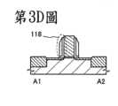
第3A至3H圖為繪示製造半導體裝置的步驟之剖面圖;Figures 3A to 3H are cross-sectional views showing the steps of manufacturing a semiconductor device;
第4A至4G圖為繪示製造半導體裝置的步驟之剖面圖;Figures 4A to 4G are cross-sectional views showing the steps of manufacturing a semiconductor device;
第5A至5D圖為繪示製造半導體裝置的步驟之剖面圖;Figures 5A to 5D are cross-sectional views showing the steps of manufacturing a semiconductor device;
第6圖為半導體裝置之剖面圖;Figure 6 is a cross-sectional view of a semiconductor device;
第7A及7B圖各為繪示半導體裝置之剖面圖;Figures 7A and 7B are cross-sectional views of semiconductor devices;
第8A及8B圖各為繪示半導體裝置之剖面圖;Figures 8A and 8B are cross-sectional views of semiconductor devices;
第9A及9B圖各為繪示半導體裝置之剖面圖;Figures 9A and 9B are cross-sectional views of semiconductor devices;
第10A至10F圖各繪示電子裝置;Figures 10A to 10F each illustrate an electronic device;
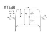
第11圖為包括氧化物半導體之反交錯型電晶體的剖面圖;Figure 11 is a cross-sectional view of an inverted staggered transistor including an oxide semiconductor;
第12A及12B圖為第11圖中之剖面A-A’的能帶圖(示意圖);Figures 12A and 12B are energy band diagrams (schematic diagrams) of the cross section A-A’ in Figure 11;
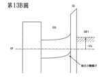
第13A圖繪示其中施加正電位(+VG)至閘極(GE1)的狀態,以及第13B圖繪示其中施加負電位(-VG)至閘極(GE1)的狀態;FIG. 13A shows a state in which a positive potential (+VG ) is applied to the gate (GE1), and FIG. 13B shows a state in which a negative potential (-VG ) is applied to the gate (GE1);
第14圖繪示繪示真空能階、金屬的工作函數(φM)、及氧化物半導體之電子親和力(χ)之關係;FIG. 14 shows the relationship between the vacuum energy level, the work function of metal (φM ), and the electron affinity (χ) of oxide semiconductors;
第15A及15B圖為半導體裝置的電路圖;Figures 15A and 15B are circuit diagrams of semiconductor devices;
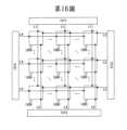
第16圖為半導體裝置的電路圖;Figure 16 is a circuit diagram of a semiconductor device;
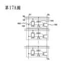
第17A及17B圖為半導體裝置的電路圖;Figures 17A and 17B are circuit diagrams of semiconductor devices;
第18A至18C圖為半導體裝置的電路圖;Figures 18A to 18C are circuit diagrams of semiconductor devices;
第19圖為半導體裝置的電路圖;Figure 19 is a circuit diagram of a semiconductor device;
第20圖為繪示電位關係的時序圖;Figure 20 is a timing diagram showing the potential relationship;
第21圖為半導體裝置的電路圖;Figure 21 is a circuit diagram of a semiconductor device;
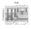
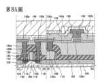
第22A及22B圖為繪示半導體裝置的剖面圖及平面圖;Figures 22A and 22B are cross-sectional views and plan views of semiconductor devices;
第23A至23D圖為繪示半導體裝置的剖面圖;Figures 23A to 23D are cross-sectional views of semiconductor devices;
第24A至24C圖為繪示半導體裝置的剖面圖;Figures 24A to 24C are cross-sectional views showing semiconductor devices;
第25圖為顯示包括氧化物半導體之電晶體的特性之圖;Figure 25 is a diagram showing the characteristics of a transistor including an oxide semiconductor;
第26圖為評估包括氧化物半導體之電晶體的特性之電路圖;Figure 26 is a circuit diagram for evaluating the characteristics of a transistor including an oxide semiconductor;
第27圖為評估包括氧化物半導體之電晶體的特性之時序圖;Figure 27 is a timing diagram for evaluating the characteristics of transistors including oxide semiconductors;
第28圖為顯示包括氧化物半導體之電晶體的特性之圖;Figure 28 is a diagram showing the characteristics of a transistor including an oxide semiconductor;
第29圖為顯示包括氧化物半導體之電晶體的特性之圖;Figure 29 is a diagram showing the characteristics of a transistor including an oxide semiconductor;
第30圖為顯示包括氧化物半導體之電晶體的特性之圖;以及Figure 30 is a diagram showing the characteristics of a transistor including an oxide semiconductor; and
第31圖為顯示記憶體窗寬度之評估結果的圖。Figure 31 is a diagram showing the evaluation results of the memory window width.
將參考附圖於下說明本發明之實施例的實例。注意到本發明不限於下列說明,且熟悉此技藝人士輕易了解到可以各種方式修改在此揭露的模式及細節而不背離本發明之精神與範疇。因此,本發明不應解釋成限於包括在此之實施例的內容。Examples of embodiments of the present invention will be described below with reference to the attached drawings. Note that the present invention is not limited to the following description, and that those skilled in the art will readily appreciate that the modes and details disclosed herein may be modified in various ways without departing from the spirit and scope of the present invention. Therefore, the present invention should not be construed as being limited to the contents of the embodiments included herein.
注意到在某些情況中為了方便了解而未準確地表示圖中所示之各個結構的位置、大小、範圍、或之類的。因此,本發明之實施例不一定限於圖中所揭露之這類位置、大小、範圍、或之類的。Note that in some cases, the position, size, range, or the like of each structure shown in the figure is not accurately indicated for the sake of convenience. Therefore, the embodiments of the present invention are not necessarily limited to such positions, sizes, ranges, or the like disclosed in the figure.
在此說明書中,使用諸如「第一」、「第二」、及「第三」的順序數以避免混淆構件,且這些用詞不意味構件數量之限制。In this specification, ordinal numbers such as "first", "second", and "third" are used to avoid confusion between components, and these terms do not imply a limitation on the number of components.
(實施例1)(Implementation Example 1)
在此實施例中,將參照第1圖、第2A和2B圖、第3A至3H圖、第4A至4G圖、第5A至5D圖、第6圖、第7A和7B圖、第8A和8B圖、及第9A和9B圖說明在此揭露之根據本發明之一實施例的結構及半導體裝置的製造方法。In this embodiment, the structure and the method for manufacturing a semiconductor device according to one embodiment of the present invention disclosed herein will be described with reference to FIG. 1, FIG. 2A and FIG. 2B, FIG. 3A to FIG. 3H, FIG. 4A to FIG. 4G, FIG. 5A to FIG. 5D, FIG. 6, FIG. 7A and FIG. 7B, FIG. 8A and FIG. 8B, and FIG. 9A and FIG. 9B.
<半導體裝置之電路組態><Circuit configuration of semiconductor devices>
第1圖繪示半導體裝置之電路組態的一實例。半導體裝置包括使用非氧化物半導體(如矽)的材料所形成之電晶體160,及使用氧化物半導體所形成之電晶體162。注意到第1圖中所示之半導體裝置在下列說明中之某些情況中稱為記憶胞。FIG. 1 shows an example of a circuit configuration of a semiconductor device. The semiconductor device includes a
在此,電晶體160的閘極電極電連接至電晶體162的源極電極和汲極電極之一。第一線(亦稱為源極線SL)電連接至電晶體160的源極電極。第二線(亦稱為位元線BL)電連接至電晶體160的汲極電極。第三線(亦稱為第一信號線)電連接至電晶體162的源極電極和汲極電極之另一。第四線(亦稱為第二信號線)電連接至電晶體162的閘極電極。Here, the gate electrode of
由於包括非氧化物半導體層的材料之電晶體160可在比包括氧化物半導體層之電晶體更高的速度操作,可藉由使用電晶體160來以高速讀出已儲存的資料。此外,包括氧化物半導體層的電晶體162具有極低的關閉電流。針對那些原因,可藉由關閉電晶體162來將電晶體160的閘極電極之電位保持極長的時間。此外,在包括氧化物半導體層之電晶體162中,不會發生短通道效應,其又是一個優點。Since the
使用可保持閘極電極之電位的優點,可以下列方式執行資料的寫入、保持、及讀取。Taking advantage of the gate electrode potential that can be maintained, data can be written, retained, and read in the following manner.
首先,將說明資料的寫入及保持。首先,將第四線之電位設定在會啟通電晶體162的電位,並啟通電晶體162。因此,將第三線之電位供應至電晶體160的閘極電極(寫入)。之後,將第四線的電位設置在會關閉電晶體162的電位,並關閉電晶體162,藉此保持電晶體160的閘極電極之電位(保持)。First, the writing and holding of data will be described. First, the potential of the fourth line is set to a potential that turns on
由於電晶體162之關閉電流極低,可保持電晶體160之閘極電極的電位極長的時間。例如,當電晶體160之閘極電極的電位為會啟通電晶體160之電位時,可長時間維持電晶體160之啟通狀態。此外,當電晶體160之閘極電極的電位為會關閉電晶體160之電位時,可長時間維持電晶體160之關閉狀態。Since the off current of
再來將說明資料之讀取。當在其中如上述般維持電晶體160的啟通狀態或關閉狀態之狀態中將預定電位(低電位)供應至第一線時,第二線之電位隨電晶體160的啟通狀態或關閉狀態而變。例如,當電晶體160啟通時,第二線的電位在第一線之電位影響下變成較低。相反地,當電晶體160關閉時,第二線的電位不改變。Next, the reading of data will be described. When a predetermined potential (low potential) is supplied to the first line in a state in which the on state or off state of the
依此方式,在其中保持資料之狀態中互相比較第二線的電位與預定電位,藉此可讀出資料。In this way, the potential of the second line and the predetermined potential are compared with each other in the state where the data is retained, thereby reading the data.
第三,將說明資料的重寫。以和資料之寫入和保持類似的方式來執行資料的重寫。亦即,將第四線的電位設定在啟通電晶體162的電位,並啟通電晶體162。因此,將第三線之電位(新資料的電位)供應至電晶體160的閘極電極。之後,將第四線的電位設定在關閉電晶體162的電位,並關閉電晶體162,藉此儲存新資料。Third, the rewriting of data will be described. The rewriting of data is performed in a similar manner to the writing and maintaining of data. That is, the potential of the fourth line is set to the potential of turning on
在於此揭露之根據本發明的半導體裝置中,可藉由如上述般的另一資料寫入來直接重寫資料。針對那個原因,無需快閃記憶體或之類所必要的抹除操作,因此可防止抹除操作所導致之操作速度的減低。換言之,可實現半導體裝置的高速操作。In the semiconductor device according to the present invention disclosed herein, data can be directly rewritten by writing another data as described above. For that reason, there is no need for an erase operation required by a flash memory or the like, thereby preventing a decrease in operating speed caused by an erase operation. In other words, high-speed operation of the semiconductor device can be achieved.
由於包括氧化物半導體層之電晶體162的針對寫入之關閉電流極小,可長時間保持電晶體160的閘極電極之電位。因此,例如,可無需傳統DRAM所需之更新操作,或者更新操作的頻率可顯著地低(如大約每一個月或一年一次)。故,根據揭露之發明的半導體裝置實質上具有非依電性記憶體裝置的特徵。Since the turn-off current of the
此外,在揭露之發明的半導體裝置中,不像傳統DRAM,當讀取資料時資料不會喪失;故在每次讀取操作中無需重寫資料。如上述,相較於DRAM可大幅減少資料寫入頻率,其允許充分降低耗電量。In addition, in the disclosed semiconductor device, unlike conventional DRAM, data is not lost when reading data; therefore, there is no need to rewrite data in each read operation. As mentioned above, the frequency of data writing can be greatly reduced compared to DRAM, which allows for a substantial reduction in power consumption.
此外,針對揭露之發明的半導體裝置,可藉由重寫新資料至半導體裝置來直接重寫資料。因此,無需快閃記憶體或之類所必要的抹除操作,並可抑制操作速度的減低(其歸因於抹除操作)。換言之,可實現半導體裝置的高速操作。另外,無需傳統浮置閘極電晶體所需之高電壓以寫入及抹除資料;故可進一步減低半導體裝置之耗電量。In addition, for the semiconductor device disclosed in the invention, data can be directly rewritten by rewriting new data to the semiconductor device. Therefore, there is no need for the erase operation required by flash memory or the like, and the reduction in operating speed (which is attributed to the erase operation) can be suppressed. In other words, high-speed operation of the semiconductor device can be achieved. In addition, the high voltage required by the traditional floating gate transistor is not required to write and erase data; therefore, the power consumption of the semiconductor device can be further reduced.
根據揭露之發明的半導體裝置可包括至少一寫入電晶體及一讀取電晶體;故相較於需要每一記憶胞六個電晶體之SRAM或之類的,每一記憶胞之面積夠小。換言之,可以高密度配置這類半導體裝置。The semiconductor device according to the disclosed invention may include at least one write transistor and one read transistor; therefore, compared to SRAM or the like which requires six transistors per memory cell, the area of each memory cell is small enough. In other words, such semiconductor devices can be configured at a high density.
在傳統浮置閘極電晶體中,於寫入操作期間電荷行於閘極絕緣層(隧道絕緣薄膜)之中,因此無法避免閘極絕緣層(隧道絕緣薄膜)之惡化。相反地,在根據本發明之一實施例的記憶胞中,藉由寫入電晶體的切換操作來寫入資料,故可忽略閘極絕緣薄膜的惡化(這傳統以來被視為是一問題)。此意味著原則上無寫入次數的限制且寫入耐久性非常高。例如,即使在寫入資料1×10⁹或更多次(一億或更多次)之後,電流-電壓特性仍未惡化。In conventional floating gate transistors, charge flows in the gate insulating layer (tunnel insulating film) during the write operation, so deterioration of the gate insulating layer (tunnel insulating film) cannot be avoided. In contrast, in a memory cell according to one embodiment of the present invention, data is written by switching the write transistor, so deterioration of the gate insulating film (which has traditionally been considered a problem) can be ignored. This means that there is no limit to the number of writes in principle and the write endurance is very high. For example, even after writing
注意到針對寫入的包括半導體裝置的電晶體162之場效遷移率,在啟通狀態中,為3cm2/Vs至250cm2/Vs(包括這兩值);較佳為5cm2/Vs至200cm2/Vs(包括這兩值);更佳為10cm2/Vs至150cm2/Vs(包括這兩值)。此外,包括氧化物半導體層之電晶體的次臨界擺幅(S值)設定成0.1V/dec或更少。藉由使用這類電晶體,資料寫入所需的時間可夠短。Note that the field effect mobility of the
針對寫入的包括半導體裝置的電晶體162之通道長度L較佳為10nm至400nm(包括這兩值)。以這類通道大小,可獲得各種功效,如高速操作、低耗電量、及電晶體之高整合。The channel length L of the
注意到包括結晶矽之電晶體較佳用為針對讀取之電晶體160。尤其,以增加讀取操作之速度來說,較佳使用包括單晶矽之n通道電晶體。可使用例如塊矽(所謂的矽晶圓)來形成這類單晶矽電晶體。Note that a transistor including crystalline silicon is preferably used as the
注意到在上述說明中使用n通道電晶體;不用說可取代n通道電晶體而使用p通道電晶體。Note that n-channel transistors are used in the above description; it goes without saying that p-channel transistors can be used instead of n-channel transistors.
<半導體裝置之平面結構及剖面結構><Planar structure and cross-sectional structure of semiconductor devices>
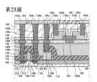
第2A及2B繪示半導體裝置之結構的一實例。第2A圖繪示半導體裝置的剖面圖,且第2B圖繪示半導體裝置的平面圖。在此,第2A圖對應沿著至第2B圖中之線A1-A2及線B1-B2的剖面。第2A及2B圖中所示之半導體裝置包括在下部中之包括非氧化物半導體裝置的材料之電晶體160,及在上部中之包括氧化物半導體層的電晶體162。注意到在此電晶體160及162為n通道電晶體;替代地,可使用p通道電晶體。尤其,很容易使用p通道電晶體作為電晶體160。Figures 2A and 2B illustrate an example of a structure of a semiconductor device. Figure 2A illustrates a cross-sectional view of the semiconductor device, and Figure 2B illustrates a plan view of the semiconductor device. Here, Figure 2A corresponds to a cross section along line A1-A2 and line B1-B2 in Figure 2B. The semiconductor device shown in Figures 2A and 2B includes a
電晶體160包括設置在包括半導體材料之基板100中的通道形成區域116、設置以夾住通道形成區域116之雜質區域114和高濃度雜質區域120(這些區域簡單統稱為雜質區域)、設置在通道形成區域116上方之閘極絕緣層108、設置在閘極絕緣層108上方之閘極電極110、及電連接至雜質區域114的源極電極或汲極電極(此後稱為源極/汲極電極)130a和源極/汲極電極130b。The
側壁絕緣層118設置在閘極電極110的一側表面上。高濃度雜質區域120放置在不與側壁絕緣層118重疊之基板100的一區域中,如剖面圖中所示。金屬化合物區域124設置在高濃度雜質區域120上方。元件隔離絕緣層106設置在基板100上方以圍繞電晶體160。設置層間絕緣層126及層間絕緣層128以覆蓋電晶體160。源極/汲極電極130a及源極/汲極電極130b的每一者經由形成在層間絕緣層126及128中的開口電連接至金屬化合物區域124。亦即,源極/汲極電極130a及源極/汲極電極130b的每一者經由金屬化合物區域124電連接至高濃度雜質區域120及雜質區域114。以和源極/汲極電極130a及130b類似方式形成的電極130c電連接至閘極電極110。The
電晶體162包括設置在層間絕緣層128上方之閘極電極136d、設置在閘極電極136d上方的閘極絕緣層138、設置在閘極絕緣層138上方之氧化物半導體層140、及設置在氧化物半導體層140上方並電連接至氧化物半導體層140的源極/汲極電極142a及源極/汲極電極142b。The
在此,設置閘極電極136d以嵌入形成在層間絕緣層128上方的絕緣層132中。像是閘極電極136d,形成分別與源極/汲極電極130a、源極/汲極電極130b、及電極130c接觸之電極136a、電極136b、及電極136c。Here, the
保護絕緣層144設置在電晶體162上方以接觸氧化物半導體層140之部分。層間絕緣層146設置在保護絕緣層144上方。到達源極/汲極電極142a和源極/汲極電極142b之開口形成在保護絕緣層144和層間絕緣層146之中。形成分別經由個別開口與源極/汲極電極142a和源極/汲極電極142b接觸之電極150d及電極150e。像是電極150d及電極150e,形成分別經由設置在閘極絕緣層138、保護絕緣層144、及層間絕緣層146中的開口與電極136a、電極136b、及電極136c接觸的電極150a、電極150b、及電極150c。A protective insulating
在此,氧化物半導體層140較佳為從其充分移除如氫之雜質的高度純化氧化物半導體層。詳言之,氧化物半導體層140中之氫濃度為5×10¹⁹atoms/cm3或更少;較佳為5×1018atoms/cm3或更少;更佳為5×1017atoms/cm3或更少。與具有近乎1×1014/cm3之載子濃度的一般矽晶圓(添加微量磷或硼之雜質的矽晶圓)相比,這類極低的氫濃度造成夠低載子濃度(如小於1×1012/cm3或1.45×1010/cm3)。可使用這類氧化物半導體來獲得具有顯著優異關閉電流特性之電晶體162,該氧化物半導體藉由充分減少氫濃度來高度純化且變成本質(i型)或實質本質(i型)。例如,電晶體162之關閉電流(在此每單位通道寬度(1μm))在室溫(25℃)為10zA/μm(1zA(賽普托安培(zeptoampere))為1×10-21A)或更少;較佳為1zA/μm或更少。電晶體162的關閉電流在85℃為100zA/μm(1×10-19A/μm)或更少;較佳為10zA/μm(1×10-20A/μm)或更少。使用藉由充分減少氫濃度而變成本質或實質本質的氧化物半導體層140以減少電晶體162的關閉電流,藉此可實現具有新穎結構的半導體裝置。注意到藉由二次離子質譜(SIMS)來測量氧化物半導體層140中之氫濃度。Here, the
絕緣層152設置在層間絕緣層146上方。設置電極154a、電極154b、電極154c、及電極154d以加以嵌入絕緣層152。電極154a與電極150a接觸。電極154b與電極150b接觸。電極154c與電極150c及電極150d接觸。電極154d與電極150e接觸。The insulating
亦即,在第2A及2B圖中所示之半導體裝置中,電晶體162之閘極電極110及電晶體162之源極/汲極電極142a經由電極130c、136c、150c、154c、及150d電連接。That is, in the semiconductor device shown in FIGS. 2A and 2B, the
<製造半導體裝置之方法><Method for manufacturing semiconductor device>
接下來,將說明製造半導體裝置之方法的一實例。首先,將參照第3A至3H圖於下說明製造在下部中之電晶體160的方法,並接著將參照第4A至4G圖及第5A至5D圖說明製造在上部中之電晶體162的方法。Next, an example of a method for manufacturing a semiconductor device will be described. First, a method for manufacturing
<製造下電晶體之方法><Method for manufacturing lower transistor>
首先,備置包括半導體材料之基板100(參見第3A圖)。作為包括半導體材料之基板100,可使用以矽、碳化矽、或之類製成之單晶半導體基板或多晶半導體基板、以鍺化矽或之類製成的化合物半導體基板、SOI基板、或之類的。在此,說明使用單晶矽基板作為包括半導體材料之基板100的一實例。First, prepare a
在基板100上方形成充當用於形成元件隔離絕緣層之遮罩的保護層102(參見第3A圖)。作為保護層102,可例如使用氧化矽、氮化矽、氮氧化矽、或之類所形成之絕緣層。注意到在此步驟之前或之後,可將提供n型傳導性之雜質元素或提供p型傳導性之雜質元素添加至基板100以控制電晶體之臨限電壓。當包括在基板100之半導體材料為矽時,可使用磷、砷、或之類的作為提供n型傳導性之雜質。可使用硼、鋁、鎵、或之類的作為提供p型傳導性之雜質。A
接下來,藉由蝕刻來移除未以保護層102覆蓋之區域(亦即暴露區域)中之基板100的部分,使用保護層102作為遮罩。因此,形成隔離的半導體區域104(參見第3B圖)。作為蝕刻,較佳執行乾蝕刻,但可執行濕蝕刻。作為蝕刻氣體,可根據被蝕刻層的材料適當選擇蝕刻劑。Next, the portion of the
接著,形成絕緣層以覆蓋半導體區域104並選擇性移除與半導體區域104重疊之一區域中的絕緣層,以致形成元件隔離絕緣層106(參見第3B圖)。使用氧化矽、氮化矽、氮氧化矽、或之類的來形成絕緣層。作為移除絕緣層的一種方法,可採用任何蝕刻處理及如CMP之拋光處理。注意到在半導體區域104的形成之後或在元件隔離絕緣層106的形成之後移除保護層102。Next, an insulating layer is formed to cover the
接下來,在半導體區域104上方形成絕緣層,並且在絕緣層上方形成包括導電材料之層。Next, an insulating layer is formed above the
由於絕緣層後續充當閘極絕緣層,絕緣層較佳具有藉由CVD方法、濺鍍方法、或之類使用含有氧化矽、氮氧化矽、氮化矽、氧化鉿、氧化鋁、氧化鉭、或之類的薄膜的單層結構或分層結構。替代地,可以一種方式形成絕緣層使得藉由高密度電漿處理或熱氧化處理來氧化或氮化半導體區域104之一表面。可例如使用諸如He、Ar、Kr、或Xe之稀有氣體與諸如氧、氮氧化物、氨、氮、或氫的氣體之混合來執行氣體高密度電漿處理。對於絕緣層之厚度無特別限制;絕緣層可具有例如1nm至100nm(包括這兩值)的厚度。Since the insulating layer subsequently serves as a gate insulating layer, the insulating layer preferably has a single-layer structure or a layered structure using a thin film containing silicon oxide, silicon oxynitride, silicon nitride, tantalum oxide, aluminum oxide, tantalum oxide, or the like by a CVD method, a sputtering method, or the like. Alternatively, the insulating layer may be formed in such a manner that a surface of the
可使用諸如鋁、銅、鈦、鉭、或鎢之金屬材料來形成包括導電材料之層。可使用諸如含有導電材料之多晶矽的半導體材料來形成包括導電材料之層。對於形成含有導電材料之層的方法並無特別限制,且可採用諸如蒸發方法、CVD方法、濺鍍方法、或旋塗方法的各種薄膜形成方法。注意到此實施例顯示其中含有導電材料之層係使用金屬材料形成的情況之一實例。A metal material such as aluminum, copper, titanium, tungsten, or tungsten may be used to form a layer including a conductive material. A semiconductor material such as polycrystalline silicon containing a conductive material may be used to form a layer including a conductive material. There is no particular limitation on the method of forming a layer including a conductive material, and various thin film forming methods such as an evaporation method, a CVD method, a sputtering method, or a spin coating method may be used. Note that this embodiment shows an example in which a layer including a conductive material is formed using a metal material.
之後,選擇性蝕刻絕緣層及包括導電材料之層,以形成閘極絕緣層108及閘極電極110(參見第3C圖)。Thereafter, the insulating layer and the layer including the conductive material are selectively etched to form a
接下來,形成覆蓋閘極電極110的絕緣層112(參見第3C圖)。接著,藉由添加磷(P)、砷(As)、或之類的到半導體區域104來形成和基板100具有淺接面深度之雜質區域114(參見第3C圖)。注意到在此添加磷或砷以形成n通道電晶體;可在形成p通道電晶體的情況中添加諸如硼(B)或鋁(Al)之雜質。藉由形成雜質區域114,在閘極絕緣層108下方的半導體區域104中形成通道形成區域116(參見第3C圖)。在此,可適當設定所添加之雜質的濃度;當半導體元件之大小縮小很多時,較佳增加濃度。在此採用其中於絕緣層112形成之後形成雜質區域114的步驟;替代地,可在雜質區域114形成後形成絕緣層112。Next, an insulating
接下來,形成側壁絕緣層118(參見第3D圖)。形成絕緣層以覆蓋絕緣層112並接著加以高各向同性蝕刻,藉此可以自對準方式形成側壁絕緣層118。此時,較佳部分蝕刻絕緣層112以暴露出閘極電極110的頂表面及雜質區域114的頂表面。Next, a
接著,形成絕緣層以覆蓋閘極電極110、雜質區域114、側壁絕緣層118、及之類的。接下來,添加諸如磷(P)、砷(As)、或之類的至其中絕緣層與雜質區域114接觸的區域,以形成高濃度雜質區域120(參見第3E圖)。此後,移除絕緣層,並形成金屬層122以覆蓋閘極電極110、側壁絕緣層118、高濃度雜質區域120、及之類的(參見第3E圖)。可採用諸如真空蒸發方法、濺鍍方法、或旋塗方法之各種薄膜形成方法來形成金屬層122。較佳使用與包括在半導體區域104中之半導體材料起反應而成為低電阻金屬化合物的金屬材料來形成金屬層122。這類金屬材料之實例為鈦、鉭、鎢、鎳、鈷、及鉑。Next, an insulating layer is formed to cover the
接下來,執行熱處理始金屬層122與半導體材料起反應。因此,形成與高濃度雜質區域120接觸之金屬化合物區域124(參見第3F圖)。注意到當使用多晶矽或之類的來形成閘極電極110時,亦在與金屬層122接觸之閘極電極110的一區域中形成金屬化合物區域。Next, heat treatment is performed to cause the
作為熱處理,可例如採用以閃光燈之照射。雖不用說可使用另一熱處理,較佳使用可實現極短時間之熱處理的方法以改善金屬化合物之形成中的化學反應的可控性。注意到藉由金屬材料與半導體材料之反應形成金屬化合物區域,且其具有充分高的傳導性。金屬化合物區域的形成可恰當減少電阻並改善元件特性。注意到在形成金屬化合物區域124之後移除金屬層122。As heat treatment, irradiation with a flash lamp may be used, for example. Although it is needless to say that another heat treatment may be used, it is preferable to use a method that can achieve heat treatment in an extremely short time to improve the controllability of the chemical reaction in the formation of the metal compound. Note that the metal compound region is formed by the reaction of the metal material and the semiconductor material, and it has sufficiently high conductivity. The formation of the metal compound region can appropriately reduce the resistance and improve the device characteristics. Note that the
接著,形成層間絕緣層126及層間絕緣層128以覆蓋於上述步驟中形成之構件(參見第3G圖)。可使用包括諸如氧化矽、氮氧化矽、氮化矽、氧化鉿、氧化鋁、或氧化鉭的無機絕緣材料之材料來形成層間絕緣層126及128。此外,可使用諸如聚酰亞胺或丙烯酸樹脂之有機絕緣材料來形成層間絕緣層126及128。注意到在此採用層間絕緣層126及層間絕緣層128的兩層結構;然而,層間絕緣層之結構不限於此結構。在形成層間絕緣層128之後,較佳以CMP、蝕刻、或之類的來平面化層間絕緣層128的表面。Next,
接著,在層間絕緣層126及128中形成到達金屬化合物區域124的開口,並在開口中形成源極/汲極電極130a及源極/汲極電極130b(參見第3H圖)。可以一種方式形成源極/汲極電極130a及130b,例如,使得藉由PVC方法、CVD方法、或之類的在包括開口的區域中形成導電層,並接著藉由蝕刻、CMP、或之類的移除導電層之部分。Next, openings reaching the
注意到在其中藉由移除導電層之部分來形成源極/汲極電極130a及130b的情況中,較佳執行程序以平面化表面。例如,當在包括開口的一區域中形成薄鈦薄膜或薄氮化鈦薄膜並接著形成鎢薄膜以嵌入開口中時,可移除多餘的鎢、鈦、氮化鈦、或之類的並可藉由後續的CMP來改善表面的平面化。以一種方式平面化包括源極/汲極電極130a及130b之表面使得可在後續步驟中有利地形成電極、電線、絕緣層、半導體層、及之類的。Note that in the case where the source/
注意到僅在此顯示與金屬化合物區域124接觸之源極/汲極電極130a及130b;然而,亦可在此步驟中形成與閘極電極110(如第2A圖中之電極130c)及之類的電極。對於用於源極/汲極電極130a及130b之材料並無特別限制,且可使用各種導電材料。例如,可使用諸如鉬、鈦、鉻、鉭、鎢、鋁、銅、釹、或鈧之導電材料。Note that only the source/
經由上述步驟,形成使用包括半導體材料之基板100的電晶體160。注意到在上述步驟後可進一步形成電極、電線、絕緣層、或之類的。當電線具有包括一層間絕緣層及一導電層之分層結構的多層結構時,可提供高度整合的半導體裝置。Through the above steps, a
<製造上電晶體的方法><Method for manufacturing a power-on transistor>
接下來,將參照第4A至4G圖及第5A至5D圖說明在層間絕緣層128上方製造電晶體162。注意到第4A至4G圖及第5A至5D圖繪示在層間絕緣層128上方製造電極、電晶體162、及之類的步驟;故省略放置於電晶體162下方之電晶體160及之類。Next, the manufacturing of
首先,在層間絕緣層128、源極/汲極電極130a及源極/汲極電極130b、及電極130c上方形成絕緣層132(參見第4A圖)。可藉由PVD方法、CVD方法、或之類的來形成絕緣層132。可使用包括諸如氧化矽、氮氧化矽、氮化矽、氧化鉿、氧化鋁、或氧化鉭的無機絕緣材料之材料來形成絕緣層132。First, an insulating
接下來,在絕緣層132中形成到達源極/汲極電極130a及130b和電極130c的開口。此時,亦在後續將形成閘極電極136d的區域中形成一開口。接著,形成導電層134以嵌入開口中(參見第4B圖)。藉由諸如使用遮罩的蝕刻之方法來形成開口。藉由諸如使用光遮罩的曝光之方法來形成遮罩。可使用濕蝕刻或乾蝕刻來做為蝕刻;乾蝕刻較佳用於微製造中。可藉由諸如PVD方法或CVD方法的薄膜形成方法來形成導電層134。可使用諸如鉬、鈦、鉻、鉭、鎢、鋁、銅、釹、或鈧之導電材料或任何這些材料的合金或化合物(如氮化物)來形成導電層134。Next, openings are formed in the insulating
詳言之,可採用一種方法,例如,其中藉由PVD方法在包括開口的區域中形成薄鈦薄膜並藉由CVD方法形成薄氮化鈦薄膜,並且接著,形成鎢薄膜以嵌入開口之中。在此,藉由PVD方法所形成之鈦薄膜具有減少形成在下電極(在此,源極/汲極電極130a及130b、電極130c、及之類)的表面上之氧化物薄膜以降低與下電極之接觸電阻的功能。在鈦薄膜形成之後形成的氮化鈦薄膜具有防止導電材料擴散的阻障功能。在形成鈦、氮化鈦、或之類的阻障薄膜之後,可藉由鍍覆方法形成銅薄膜。In detail, a method may be adopted, for example, in which a thin titanium film is formed in a region including an opening by a PVD method and a thin titanium nitride film is formed by a CVD method, and then a tungsten film is formed to be embedded in the opening. Here, the titanium film formed by the PVD method has a function of reducing the oxide film formed on the surface of the lower electrode (here, the source/
在形成導電層134之後,藉由蝕刻、CMP、或之類來移除導電層134的部分,以暴露出絕緣層132並形成電極136a、136b、及136c和閘極電極136d(參見第4C圖)。注意到當藉由移除導電層134之部分而形成電極136a、136b、及136c和閘極電極136d時,較佳執行程序以平面化表面。以一種方式平面化絕緣層132、電極136a、136b、及136c和閘極電極136d的表面,藉此可在後續步驟中有利地形成電極、電線、絕緣層、半導體層、及之類。After forming the
接下來,形成閘極絕緣層138以覆蓋絕緣層132、電極136a、136b、及136c和閘極電極136d(參見第4D圖)。可藉由CVD方法、濺鍍方法、或之類的來形成閘極絕緣層138。較佳使用氧化矽、氮化矽、氧氮化矽、氮氧化矽、氧化鋁、氧化鉿、氧化鉭、或之類來形成閘極絕緣層138。注意到閘極絕緣層138可具有單層結構或分層結構。例如,可藉由使用矽烷(SiH4)、氧、及氮作為來源氣體之電漿CVD方法來形成以氧氮化矽製成之閘極絕緣層138。對於閘極絕緣層138之厚度並無特別限制;閘極絕緣層138可具有例如10nm至50nm(包括這兩值)的厚度。在採用分層結構的情況中,例如,閘極絕緣層138較佳為一具有50nm至200nm(包括這兩值)的厚度之第一閘極絕緣層與在第一閘極絕緣層上方之一具有5nm至300nm(包括這兩值)的厚度之第二閘極絕緣層的堆疊。Next, a
注意到藉由移除雜質之變成本質或實質本質的氧化物半導體(高度純化氧化物半導體)頗容易受到界面能階及界面電荷的影響;因此,當使用這類氧化物半導體作為氧化物半導體層時,與閘極絕緣層之界面很重要。換言之,將與高度純化氧化物半導體層接觸的閘極絕緣層138必須有高品質。Note that an oxide semiconductor (highly purified oxide semiconductor) that has become intrinsic or substantially intrinsic by removing impurities is easily affected by interface energy levels and interface charges; therefore, when such an oxide semiconductor is used as an oxide semiconductor layer, the interface with the gate insulating layer is important. In other words, the
例如,較佳藉由使用微波(2.45GHz)之高密度電漿CVD方法來形成閘極絕緣層138,因為閘極絕緣層138可為稠密且具有高耐受電壓與高品質。當高度純化氧化物半導體層與高品質閘極絕緣層互相接觸時,可減少界面能階且界面特性為有利。For example, it is preferable to form the
不用說,即使當使用高度純化氧化物半導體層時,可採用諸如濺鍍方法或電漿CVD方法的另一方法,只要可形成高品質的絕緣層作為閘極絕緣層。此外,可使用絕緣層,其與氧化物半導體層之界面的品質及特性藉由在形成絕緣層之後執行的熱處理受到改善。在任何情況中,形成具有作為閘極絕緣層138之有利的薄膜品質並可減少與氧化物半導體層之界面能階密度以形成有利界面的絕緣層作為閘極絕緣層138。Needless to say, even when a highly purified oxide semiconductor layer is used, another method such as a sputtering method or a plasma CVD method may be adopted as long as a high-quality insulating layer can be formed as a gate insulating layer. In addition, an insulating layer may be used, the quality and characteristics of the interface with the oxide semiconductor layer being improved by heat treatment performed after the insulating layer is formed. In any case, an insulating layer having a favorable film quality as a
若雜質包括在氧化物半導體中,則會由諸如高電場或高溫的應力劈開雜質與氧化物半導體的主成分間的鍵而造成懸掛鍵,其導致臨限電壓(Vth)的位移。If impurities are included in an oxide semiconductor, the bonds between the impurities and the main component of the oxide semiconductor may be cleaved by stress such as a high electric field or high temperature, resulting in hanging bonds, which causes a shift in the threshold voltage (Vth).
將包括在氧化物半導體中之雜質(尤其是氫及水)減至最小並如上述將氧化物半導體與閘極絕緣層之間的界面特性變得有利,藉此可獲得在諸如高電場及高溫的應力下為穩定之電晶體。By minimizing impurities (especially hydrogen and water) included in the oxide semiconductor and making the interface characteristics between the oxide semiconductor and the gate insulating layer favorable as described above, a transistor that is stable under stress such as high electric field and high temperature can be obtained.
接下來,在閘極絕緣層138上方形成氧化物半導體層並藉由諸如使用遮罩的蝕刻之方法加以處理,以形成島狀氧化物半導體層140(參見第4E圖)。Next, an oxide semiconductor layer is formed on the
作為氧化物半導體層,較佳使用In-Ga-Zn-O為基的氧化物半導體層、In-Sn-Zn-O為基的氧化物半導體層、In-Al-Zn-O為基的氧化物半導體層、Sn-Ga-Zn-O為基的氧化物半導體層、Al-Ga-Zn-O為基的氧化物半導體層、Sn-Al-Zn-O為基的氧化物半導體層、In-Zn-O為基的氧化物半導體層、Sn-Zn-O為基的氧化物半導體層、Al-Zn-O為基的氧化物半導體層、In-O為基的氧化物半導體層、Sn-O為基的氧化物半導體層、或Zn-O為基的氧化物半導體層。特別較佳這些氧化物半導體存在於非晶態中。在此實施例中,作為氧化物半導體層,藉由用於沉積In-Ga-Zn-O為基的氧化物半導體之使用靶材的濺鍍方法來形成非晶氧化物半導體層。注意到由於可藉由添加矽到非晶氧化物半導體層來抑制非晶氧化物半導體層的結晶,可使用例如含有在2wt%至10wt%(包括這兩值)之SiO2的靶材來形成氧化物半導體層。As the oxide semiconductor layer, it is preferred to use an In-Ga-Zn-O-based oxide semiconductor layer, an In-Sn-Zn-O-based oxide semiconductor layer, an In-Al-Zn-O-based oxide semiconductor layer, a Sn-Ga-Zn-O-based oxide semiconductor layer, an Al-Ga-Zn-O-based oxide semiconductor layer, a Sn-Al-Zn-O-based oxide semiconductor layer, an In-Zn-O-based oxide semiconductor layer, a Sn-Zn-O-based oxide semiconductor layer, an Al-Zn-O-based oxide semiconductor layer, an In-O-based oxide semiconductor layer, a Sn-O-based oxide semiconductor layer, or a Zn-O-based oxide semiconductor layer. It is particularly preferred that these oxide semiconductors exist in an amorphous state. In this embodiment, as an oxide semiconductor layer, an amorphous oxide semiconductor layer is formed by a sputtering method using a target for depositing an In-Ga-Zn-O-based oxide semiconductor. Note that since the crystallization of the amorphous oxide semiconductor layer can be suppressed by adding silicon to the amorphous oxide semiconductor layer, a target containing, for example, 2 wt % to 10 wt % (including these two values) of SiO2 can be used to form the oxide semiconductor layer.
作為藉由濺鍍方法形成氧化物半導體層用之靶材,可使用例如含有氧化鋅作為其主成分之氧化物半導體沉積靶材。此外,可使用例如含有In、Ga、及Zn(In2O3:Ga2O3:ZnO的成分比例=1:1:1[莫耳比率])之沉積氧化物半導體用的靶材。還有,可使用例如含有In、Ga、及Zn(In2O3:Ga2O3:ZnO的成分比例=1:1:2[莫耳比率]或In2O3:Ga2O3:ZnO的成分比例=1:1:4[莫耳比率])之沉積氧化物半導體用的靶材。沉積氧化物半導體用的靶材之填充率為90%至100%(包括這兩值),較佳大於或等於95%(如99.9%)。使用具有高填充率之沉積氧化物半導體用的靶材來形成稠密氧化物半導體層。As a target for forming an oxide semiconductor layer by a sputtering method, for example, an oxide semiconductor deposition target containing zinc oxide as its main component can be used. In addition, for example, a target for depositing an oxide semiconductor containing In, Ga, and Zn (the composition ratio of In2 O3 : Ga2 O3 : ZnO = 1:1:1 [molar ratio]) can be used. Furthermore, for example, a target for depositing an oxide semiconductor containing In, Ga, and Zn (the composition ratio of In2 O3 : Ga2 O3 : ZnO = 1:1:2 [molar ratio] or the composition ratio of In2 O3 : Ga2 O3 : ZnO = 1:1:4 [molar ratio]) can be used. The filling rate of the target material for depositing oxide semiconductor is 90% to 100% (including these two values), preferably greater than or equal to 95% (such as 99.9%). The target material for depositing oxide semiconductor with a high filling rate is used to form a dense oxide semiconductor layer.
其中形成氧化物半導體層之周圍環境較佳為稀有氣體(典型氬)周圍環境、氧周圍環境、或含有稀有氣體(典型氬)及氧之混合周圍環境。詳言之,較佳使用高純度氣體,例如,從其移除諸如氫、水、具有羥基或氫化物之化合物的雜質始濃度為數ppm(較佳數ppb)。The surrounding environment in which the oxide semiconductor layer is formed is preferably a rare gas (typically argon) surrounding environment, an oxygen surrounding environment, or a mixed surrounding environment containing a rare gas (typically argon) and oxygen. In detail, it is preferred to use a high-purity gas, for example, from which impurities such as hydrogen, water, compounds having hydroxyl groups or hydrides are removed to an initial concentration of several ppm (preferably several ppb).
在形成氧化物半導體層中,將基板保持在一維持在減壓之處理室中且基板溫度設定至100℃至600℃(包括這兩值),較佳200℃至400℃(包括這兩值)。在加熱基板的同時形成氧化物半導體層,而得以減少氧化物半導體層之雜質濃度。此外,減少濺鍍造成之氧化物半導體層的破壞。接著,將移除氫與水之濺鍍氣體引到已移除殘留濕氣的處理室之中,並使用金屬氧化物作為靶材來形成氧化物半導體層。較佳使用捕集真空泵以移除處理室中殘留的濕氣。例如,可使用低溫泵、離子泵、或鈦昇華泵。抽空單元可為設有冷阱的渦輪泵。在以低溫泵抽空之沉積室中,除了含有碳原子及氫原子之化合物外,移除諸如水(H2O)的含有氫原子之化合物及之類,藉此可減少形成在沉積室中之氧化物半導體層的雜質濃度。In forming an oxide semiconductor layer, the substrate is maintained in a processing chamber maintained at a reduced pressure and the substrate temperature is set to 100°C to 600°C (both inclusive), preferably 200°C to 400°C (both inclusive). The oxide semiconductor layer is formed while the substrate is heated, thereby reducing the impurity concentration of the oxide semiconductor layer. In addition, the damage to the oxide semiconductor layer caused by sputtering is reduced. Then, the sputtering gas from which hydrogen and water have been removed is introduced into the processing chamber from which residual moisture has been removed, and the oxide semiconductor layer is formed using a metal oxide as a target. It is preferred to use a capture vacuum pump to remove residual moisture in the processing chamber. For example, a cryogenic pump, an ion pump, or a titanium sublimation pump can be used. The evacuation unit may be a turbo pump equipped with a cold trap. In the deposition chamber evacuated by the cryogenic pump, compounds containing hydrogen atoms such as water (H2O ) and the like are removed in addition to compounds containing carbon atoms and hydrogen atoms, thereby reducing the impurity concentration of the oxide semiconductor layer formed in the deposition chamber.
可在下列條件下形成氧化物半導體層,例如,基板與靶材間的距離為100nm;壓力為0.6Pa;直流(DC)電源為0.5kW;且周圍環境為氧(氧流速為100%)。注意到較佳使用脈衝直流(DC)電源,因為可減少在薄膜沉積中形成的粉末物質(亦稱為粒子或塵埃)並且厚度分布可為小。氧化物半導體層之厚度為2nm至200nm(包括這兩值),較佳為5nm至30nm(包括這兩值)。注意到適當的厚度隨氧化物半導體材料而變,且根據使用之材料適當設定厚度。The oxide semiconductor layer can be formed under the following conditions, for example, the distance between the substrate and the target is 100nm; the pressure is 0.6Pa; the DC power supply is 0.5kW; and the surrounding environment is oxygen (the oxygen flow rate is 100%). Note that it is preferred to use a pulsed DC power supply because powder materials (also called particles or dust) formed in the film deposition can be reduced and the thickness distribution can be small. The thickness of the oxide semiconductor layer is 2nm to 200nm (including these two values), preferably 5nm to 30nm (including these two values). Note that the appropriate thickness varies with the oxide semiconductor material, and the thickness is appropriately set according to the material used.
注意到在藉由濺鍍方法形成氧化物半導體層之前,藉由其中引進氬氣體並產生電漿的反向濺鍍來移除閘極絕緣層138之表面上的塵埃。在此,相較於離子衝擊濺鍍靶材之正常濺鍍,反向濺鍍為一種離子衝擊欲處理之表面以修改表面的方法。讓離子衝擊欲處理之表面的方法之一實例為其中在氬周圍環境中供應高頻電壓至表面以在基板附近產生電漿的方法。注意到取代氬周圍環境,可使用氮周圍環境、氦周圍環境、氧周圍環境、或之類的。Note that before forming the oxide semiconductor layer by the sputtering method, dust on the surface of the
作為氧化物半導體層之蝕刻方法,可採用乾蝕刻或濕蝕刻。不用說可結合使用乾蝕刻及濕蝕刻。根據材料適當地設定蝕刻條件(如蝕刻氣體或蝕刻溶液、蝕刻時間、及溫度)以將氧化物半導體蝕刻成希望的形狀。As an etching method for the oxide semiconductor layer, dry etching or wet etching can be used. Needless to say, dry etching and wet etching can be used in combination. Etching conditions (such as etching gas or etching solution, etching time, and temperature) are appropriately set according to the material to etch the oxide semiconductor into a desired shape.
用於乾蝕刻的蝕刻氣體的一實例為含有氯(氯為基之氣體,如氯(Cl2)、氯化硼(BCl3)、氯化矽(SiCl4)、或四氯化碳(CCl4))之氣體。此外,可使用含氟之氣體(氟為基之氣體,如四氟化碳(CF4)、氟化硫(SF4)、氟化氮(NF3)、或三氟甲烷(CHF3))、溴化氫(HBr)、氧(O2)、或諸如(He)或(Ar)的稀有氣體可添加至其之任何這些氣體、或之類的。An example of an etching gas used for dry etching is a gas containing chlorine (chlorine-based gas such as chlorine (Cl2 ), boron chloride (BCl3 ), silicon chloride (SiCl4 ), or carbon tetrachloride (CCl4 )). In addition, a fluorine-containing gas (fluorine-based gas such as carbon tetrafluoride (CF4 ), sulfur fluoride (SF4 ), nitrogen fluoride (NF3 ), or trifluoromethane (CHF3 )), hydrogen bromide (HBr), oxygen (O2 ), or a rare gas such as (He) or (Ar) may be added to any of these gases, or the like may be used.
作為乾蝕刻方法,可使用平行板RIE(反應性離子蝕刻)方法或ICP(電感耦合式電漿)蝕刻方法。為了蝕刻氧化物半導體層至希望的形狀,適當地設定蝕刻條件(如供應至盤繞電極之電力量、供應至基板側上之電極的電力量、及基板側上之電極溫度)。As a dry etching method, a parallel plate RIE (reactive ion etching) method or an ICP (inductively coupled plasma) etching method can be used. In order to etch the oxide semiconductor layer into a desired shape, etching conditions (such as the amount of power supplied to the winding electrode, the amount of power supplied to the electrode on the substrate side, and the temperature of the electrode on the substrate side) are appropriately set.
作為濕蝕刻的蝕刻劑,可使用磷酸、醋酸、及硝酸或之類的混合溶液。亦可使用如ITO07N(由KANTO CHEMICAL CO.,INC所生產)之蝕刻劑。As wet etching etchants, phosphoric acid, acetic acid, nitric acid or mixed solutions thereof can be used. Etching agents such as ITO07N (produced by KANTO CHEMICAL CO., INC) can also be used.
接著,較佳於氧化物半導體層上執行第一熱處理。可以第一熱處理脫水或脫氫氧化物半導體層。第一熱處理的溫度大於或等於300℃且小於或等於750℃,較佳大於或等於400℃且小於基板之應變點。例如,將基板引進到電爐中,其中使用電阻式加熱元件或之類的,並且使氧化物半導體層140在450℃於氮周圍環境中受到加熱處理一小時。氧化物半導體層140在熱處理期間未暴露至空氣,所以可防止水及氫的進入。Next, a first heat treatment is preferably performed on the oxide semiconductor layer. The oxide semiconductor layer can be dehydrated or dehydrogenated by the first heat treatment. The temperature of the first heat treatment is greater than or equal to 300°C and less than or equal to 750°C, preferably greater than or equal to 400°C and less than the strain point of the substrate. For example, the substrate is introduced into an electric furnace, in which a resistive heating element or the like is used, and the
熱處理設備不限於電爐且可為藉由熱輻射或熱傳導從諸如加熱氣體的一媒介加熱物體之設備。例如,可使用諸如氣體迅速熱退火(GRTA)設備或燈迅速熱退火(LRTA)設備的迅速熱退火(RTA)設備。LRTA設備為藉由從諸如鹵素燈、金屬鹵化物、氙弧燈、碳弧燈、高壓鈉燈、或高壓汞燈的燈所發射之光的輻射(電磁波)加熱待處理物體之設備。GRTA設備為使用高溫氣體來執行熱處理的設備。作為氣體,使用不藉由熱處理與物體起反應之例如氮的惰性氣體或諸如氬之稀有氣體。The heat treatment apparatus is not limited to an electric furnace and may be an apparatus that heats an object by thermal radiation or heat conduction from a medium such as a heating gas. For example, a rapid thermal annealing (RTA) apparatus such as a gas rapid thermal annealing (GRTA) apparatus or a lamp rapid thermal annealing (LRTA) apparatus may be used. The LRTA apparatus is an apparatus that heats an object to be treated by radiation (electromagnetic waves) of light emitted from a lamp such as a halogen lamp, a metal halide, a xenon arc lamp, a carbon arc lamp, a high-pressure sodium lamp, or a high-pressure mercury lamp. The GRTA apparatus is an apparatus that performs heat treatment using a high-temperature gas. As the gas, an inert gas such as nitrogen or a rare gas such as argon which does not react with the object by heat treatment is used.
例如,作為第一熱處理,可如下般執行GRTA程序。將基板放置在已加熱至650℃至700℃的高溫之惰性氣體中,加熱數分鐘,並從惰性氣體中取出。GRTA程序允許短時的高溫加熱處理。此外,即使當溫度超過基板的應變點時,仍可採用GRTA程序,因為其為短時間的熱處理。For example, as the first heat treatment, the GRTA process can be performed as follows. The substrate is placed in an inert gas heated to a high temperature of 650°C to 700°C, heated for several minutes, and removed from the inert gas. The GRTA process allows a short-term high-temperature heat treatment. In addition, the GRTA process can be used even when the temperature exceeds the strain point of the substrate because it is a short-term heat treatment.
注意到第一熱處理較佳在含有氮或稀有氣體(如氦、氖、或氬)作為主成分且不含水、氫、或之類的周圍環境中執行。例如,引進熱處理室中之氮或諸如氦、氖、或氬之稀有氣體的純度較佳大於或等於6N(99.9999%),更佳大於或等於7N(99.99999%)(亦即,雜質濃度小於或等於1ppm,較佳小於或等於0.1ppm)。Note that the first heat treatment is preferably performed in an ambient environment containing nitrogen or a rare gas (such as helium, neon, or argon) as a main component and free of water, hydrogen, or the like. For example, the purity of nitrogen or a rare gas such as helium, neon, or argon introduced into the heat treatment chamber is preferably greater than or equal to 6N (99.9999%), more preferably greater than or equal to 7N (99.99999%) (i.e., the impurity concentration is less than or equal to 1ppm, preferably less than or equal to 0.1ppm).
根據第一熱處理之條件或氧化物半導體層之材料,有時氧化物半導體層結晶成微晶或多晶。例如,氧化物半導體層有時變成具有90%或更多,或80%或更多的結晶程度之微晶氧化物半導體層。另外,根據第一熱處理之條件或氧化物半導體層之材料,氧化物半導體層可微不含結晶成分的非晶氧化物半導體層。Depending on the conditions of the first heat treatment or the material of the oxide semiconductor layer, the oxide semiconductor layer may be crystallized into microcrystals or polycrystals. For example, the oxide semiconductor layer may become a microcrystalline oxide semiconductor layer having a crystallinity of 90% or more, or 80% or more. In addition, depending on the conditions of the first heat treatment or the material of the oxide semiconductor layer, the oxide semiconductor layer may become an amorphous oxide semiconductor layer containing no crystalline component.
此外,氧化物半導體層有時變成其中微晶(粒度為1nm至20nm(包括這兩值),典型為2nm至4nm(包括這兩值))混合在非晶氧化物半導體(如氧化物半導體層的表面)中的層。In addition, the oxide semiconductor layer sometimes becomes a layer in which microcrystals (grain size of 1 nm to 20 nm both inclusive, typically 2 nm to 4 nm both inclusive) are mixed in an amorphous oxide semiconductor (such as the surface of the oxide semiconductor layer).
可藉由對準氧化物半導體層之非晶區域中的微晶來改變氧化物半導體層的電氣特性。例如,當使用沉積In-Ga-Zn-O為基的氧化物半導體用之靶材來形成氧化物半導體層時,可藉由形成微晶部分(其中具有電各向異性之In2Ga2ZnO7的晶粒為對準)來改變氧化物半導體之電氣特性。The electrical characteristics of the oxide semiconductor layer can be changed by aligning microcrystals in the amorphous region of the oxide semiconductor layer. For example, when the oxide semiconductor layer is formed using a target for depositing an In-Ga-Zn-O-based oxide semiconductor, the electrical characteristics of the oxide semiconductor can be changed by forming a microcrystal portion in which grains of In2 Ga2 ZnO7 having electrical anisotropy are aligned.
詳言之,例如,當配置晶粒使得In2Ga2ZnO7的c軸與氧化物半導體層之表面垂直時,可改善與氧化物半導體層平行之方向中的傳導性並可改善與氧化物半導體層之表面垂直之方向中的絕緣性質。此外,這類微晶部分具有抑制諸如水或氫的雜質進入氧化物半導體層中的功能。Specifically, for example, when the crystal grains are arranged so that the c-axis of In2 Ga2 ZnO7 is perpendicular to the surface of the oxide semiconductor layer, the conductivity in the direction parallel to the oxide semiconductor layer can be improved and the insulation property in the direction perpendicular to the surface of the oxide semiconductor layer can be improved. In addition, such a microcrystalline portion has the function of inhibiting impurities such as water or hydrogen from entering the oxide semiconductor layer.
注意到可藉由以GRTA程序加熱氧化物半導體層來形成包括微晶部分之氧化物半導體層。此外,可藉由使用其中Zn量小於In或Ga量之濺鍍靶材以更佳的方式來形成氧化物半導體層。It is noted that an oxide semiconductor layer including a microcrystalline portion can be formed by heating the oxide semiconductor layer by a GRTA process. In addition, the oxide semiconductor layer can be formed in a better manner by using a sputtering target in which the amount of Zn is smaller than the amount of In or Ga.
可在尚未處理成島狀氧化物半導體層140的氧化物半導體層上執行氧化物半導體層140之第一熱處理。在那個情況中,在第一熱處理之後,從加熱設備取出基板並執行光微影步驟。The first heat treatment of the
注意到第一熱處理可稱為脫水處理、脫氫處理、或之類的,因其對氧化物半導體層140之脫水或脫氫的效果的緣故。可在例如形成氧化物半導體層、在氧化物半導體層140上方堆疊源極電極和汲極電極之後、或在源極和汲極電極上方形成保護絕緣層之後,執行這類脫水處理或脫氫處理。可執行這類脫水處理或脫氫處理一次或數次。Note that the first heat treatment may be referred to as a dehydration treatment, a dehydrogenation treatment, or the like, due to its effect on dehydration or dehydrogenation of the
接下來,形成與氧化物半導體層140接觸之源極/汲極電極142a及源極/汲極電極142b(參見第4F圖)。可以一種方式形成源極/汲極電極142a及142b以形成導電層以覆蓋氧化物半導體層140並接著加以選擇性蝕刻。Next, source/
可藉由諸如濺鍍方法之PVD方法或諸如電漿CVD方法的CVD方法來形成導電層。作為導電層的材料,可使用選自鋁、鉻、銅、鉭、鈦、鉬、或鎢之元素、任何這些元素作為成分之合金、或之類的。還有,可使用選自錳、鎂、鋯、鈹、或釷的一或更多材料。可使用與選自鈦、鉭、鎢、鉬、鉻、釹、或鈧的一或更多元素結合的鋁。導電層可為單層結構或包括兩或更多層之分層結構。例如,導電層可具有含矽之鋁薄膜的單層結構、其中鈦薄膜堆疊在鋁薄膜之上的兩層結構、或其中鈦薄膜、鋁薄膜、及鈦薄膜以此順序堆疊的三層結構。The conductive layer may be formed by a PVD method such as a sputtering method or a CVD method such as a plasma CVD method. As a material for the conductive layer, an element selected from aluminum, chromium, copper, tungsten, molybdenum, titanium, molybdenum, or tungsten, an alloy of any of these elements as a component, or the like may be used. Also, one or more materials selected from manganese, magnesium, zirconium, curium, or thorium may be used. Aluminum combined with one or more elements selected from titanium, tungsten, molybdenum, chromium, neodymium, or niobium may be used. The conductive layer may be a single-layer structure or a layered structure including two or more layers. For example, the conductive layer may have a single-layer structure of a silicon-containing aluminum film, a two-layer structure in which a titanium film is stacked on an aluminum film, or a three-layer structure in which a titanium film, an aluminum film, and a titanium film are stacked in this order.
在此,較佳使用紫外線光、KrF雷射光、或ArF雷射光於形成用於蝕刻之遮罩的曝光。Here, it is preferred to use ultraviolet light, KrF laser light, or ArF laser light for exposure to form a mask for etching.
藉由源極/汲極電極142a之下邊緣部與源極/汲極電極142b之下邊緣部之間的距離來決定電晶體之通道長度(L)。注意到在通道長度(L)小於25nm的情況中之曝光,以極紫外射線(其之波長為極短的數奈米至數百奈米)執行形成遮罩的曝光。極紫外射線之曝光的解低度為高且焦深為大。針對這些原因,後續形成之電晶體之通道長度(L)可在10nm至1000nm的範圍中,且可在較高的速度操作電路。此外,關閉電流極低,其防止耗電量增加。The channel length (L) of the transistor is determined by the distance between the lower edge of the source/
適當調整導電層極氧化物半導體層140之材料和蝕刻條件,使得在導電層之蝕刻中不會移除氧化物半導體層140。注意到在某些情況中,根據材料及蝕刻條件,在蝕刻步驟中部分蝕刻氧化物半導體層140且其因此具有溝槽部分(凹部)。The material and etching conditions of the conductive layer and the
可在氧化物半導體層140與源極/汲極電極142a之間和氧化物半導體層140與源極/汲極電極142b之間形成氧化物導電層。可陸續形成氧化物導電層及用於形成源極/汲極電極142a及142b之金屬層。氧化物導電層可作為源極區域及汲極區域。這類氧化物導電層之設置可減少源極區域及汲極區域的電阻,使電晶體可在高速度操作。An oxide conductive layer may be formed between the
為了減少將使用之遮罩的數量並減少步驟數量,可使用以多色調遮罩形成之阻劑遮罩來執行蝕刻步驟,該多色調遮罩為透過其透射的光具有複數強度之曝光遮罩。使用多色調遮罩而形成的阻劑遮罩具有複數厚度(具有像階梯之形狀)且進一步可藉由灰化來改變形狀;因此,阻劑遮罩可用在用於處理成不同形狀的複數蝕刻步驟中。亦即,可藉由使用多色調遮罩來形成對應至至少兩種不同圖案的阻劑遮罩。故可減少曝光遮罩的數量且亦可減少對應光微影步驟之數量,藉此簡化程序。In order to reduce the number of masks to be used and reduce the number of steps, a resist mask formed with a multi-tone mask, which is an exposure mask through which light transmitted has multiple intensities, can be used to perform the etching step. The resist mask formed using the multi-tone mask has multiple thicknesses (having a shape like a step) and can further change the shape by ashing; therefore, the resist mask can be used in multiple etching steps for processing into different shapes. That is, a resist mask corresponding to at least two different patterns can be formed by using a multi-tone mask. Therefore, the number of exposure masks can be reduced and the number of corresponding photolithography steps can also be reduced, thereby simplifying the procedure.
注意到在上述步驟之後較佳使用諸如N2O、N2、或Ar的氣體來執行電漿處理。此電漿處理移除附接至氧化物半導體層之暴露表面的水或之類的。可使用氧及氬的混合氣體來執行電漿處理。Note that it is preferable to perform plasma treatment using a gas such as N2 O, N2 , or Ar after the above steps. This plasma treatment removes water or the like attached to the exposed surface of the oxide semiconductor layer. The plasma treatment may be performed using a mixed gas of oxygen and argon.
接下來,形成與未暴露至空氣的氧化物半導體層140之部分接觸的保護絕緣層144(參見第4G圖)。Next, a protective
可藉由一種方法來形成保護絕緣層144,藉此防止諸如水及氫的雜質混合至保護絕緣層144,適當地,例如濺鍍方法。保護絕緣層144具有至少1nm的厚度。可使用氧化矽、氮化矽、氧氮化矽、氮氧化矽、或之類的來形成保護絕緣層144。保護絕緣層144可具有單層結構或分層結構。在形成保護絕緣層144中之基板溫度較佳高於或等於室溫並低於或等於300℃。形成保護絕緣層144之周圍環境較佳為稀有氣體(典型氬)周圍環境、氧周圍環境、或含有稀有氣體(典型氬)及氧的混合周圍環境。The protective
若氫包含在保護絕緣層144中,氫可能進入氧化物半導體層中或提取氧化物半導體層中之氧,藉此可能減少在背通道側上之氧化物半導體層的電阻並可能形成寄生通道。因此,很重要地在形成保護絕緣層144中不使用氫,以使氧化物半導體層140含有盡可能少的氫。If hydrogen is contained in the protective insulating
此外,較佳在移除留在處理室中的水之同時形成保護絕緣層144,使得氫、羥基、或水不會包含在氧化物半導體層140及保護絕緣層144之中。In addition, it is preferred to form the protective insulating
較佳使用捕集真空泵以移除處理室中殘留的濕氣。例如,較佳使用低溫泵、離子泵、或鈦昇華泵。抽空單元可為設有冷阱的渦輪泵。在以低溫泵抽空之沉積室中,移除氫原子及諸如水(H2O)的含有氫原子之化合物;故可減少形成在沉積室中之保護絕緣層144的雜質濃度。It is preferred to use a capture vacuum pump to remove the residual moisture in the processing chamber. For example, it is preferred to use a cryogenic pump, an ion pump, or a titanium sublimation pump. The evacuation unit may be a turbo pump provided with a cold trap. In the deposition chamber evacuated by the cryogenic pump, hydrogen atoms and compounds containing hydrogen atoms such as water (H2O ) are removed; thus, the impurity concentration of the protective insulating
作為用於形成保護絕緣層144之濺鍍氣體,較佳使用移除了諸如氫、水、具有羥基之化合物、或氫化物的雜質之高純度氣體,使雜質濃度減少至數ppm(較佳數ppb)。As the sputtering gas used to form the protective insulating
接下來,較佳在惰性氣體周圍環境或氧氣體周圍環境(在200℃至400℃(包括這兩值),例如,在250℃至350℃(包括這兩值))中執行第二熱處理。例如,在250℃於氮周圍環境中執行第二熱處理一小時。第二熱處理可減少電晶體之電氣特性中的變異。Next, it is preferred to perform a second heat treatment in an inert gas ambient environment or an oxygen gas ambient environment (at 200°C to 400°C (both inclusive), for example, at 250°C to 350°C (both inclusive)). For example, the second heat treatment is performed at 250°C in a nitrogen ambient environment for one hour. The second heat treatment can reduce variations in the electrical characteristics of the transistor.
此外,可在100℃至200℃在空氣中執行熱處理一小時至30小時。可在固定加熱溫度執行此熱處理;替代地,可重複進行數次加熱溫度之下列改變:將加熱溫度從室溫增加至的100℃至200℃溫度並接著降至室溫。可在形成保護絕緣層之前在減壓下執行此熱處理。在減壓下可縮短熱處理的時間。取代第二熱處理可執行在減壓下的此熱處理或可在第二熱處理之前或之後執行此熱處理。In addition, heat treatment may be performed in air at 100°C to 200°C for one hour to 30 hours. This heat treatment may be performed at a fixed heating temperature; alternatively, the following change in heating temperature may be repeated several times: the heating temperature is increased from room temperature to a temperature of 100°C to 200°C and then decreased to room temperature. This heat treatment may be performed under reduced pressure before forming the protective insulating layer. The time of heat treatment may be shortened under reduced pressure. This heat treatment under reduced pressure may be performed instead of the second heat treatment or may be performed before or after the second heat treatment.
接下來,在保護絕緣層144之上形成層間絕緣層146(參見第5A圖)。可藉由PVD方法、CVD方法、或之類的來形成層間絕緣層146。可使用包括氧化矽、氮氧化矽、氮化矽、氧化鉿、氧化鋁、或氧化鉭的無機絕緣材料的材料來形成層間絕緣層146。在形成層間絕緣層146之後,較佳以CMP、蝕刻、或之類的來平面化層間絕緣層146的表面。Next, an
接下來,在層間絕緣層146、保護絕緣層144、及閘極絕緣層138中形成到達電極136a、136b、及136c和源極/汲極電極142a及142b的開口。接著,形成導電層148以嵌入開口中(參見第5B圖)。可藉由諸如使遮罩的蝕刻之方法來形成開口。可藉由諸如使用光遮罩的曝光之方法來形成遮罩。可使用濕蝕刻或乾蝕刻來做為蝕刻:以微製造而言較佳使用乾蝕刻。可藉由諸如PVD方法或CVD方法的薄膜形成方法來形成導電層148。可例如使用諸如鉬、鈦、鉻、鉭、鎢、鋁、銅、釹、或鈧之導電材料或任何這些材料的合金或化合物(如氮化物)來形成導電層148。Next, openings are formed in the
詳言之,可採用一種方法,例如,其中藉由PVD方法在包括開口的區域中形成薄鈦薄膜並藉由CVD方法形成薄氮化鈦薄膜,並且接著,形成鎢薄膜以嵌入開口之中。在此,藉由PVD方法所形成之鈦薄膜具有減少形成在下電極(在此,電極136a、136b、及136c和源極/汲極電極142a及142b)的表面上之氧化物薄膜以降低與下電極之接觸電阻的功能。在鈦薄膜形成之後形成的氮化鈦薄膜具有防止導電材料擴散的阻障功能。在形成鈦、氮化鈦、或之類的阻障薄膜之後,可藉由鍍覆方法形成銅薄膜。In detail, a method may be adopted, for example, in which a thin titanium film is formed in a region including an opening by a PVD method and a thin titanium nitride film is formed by a CVD method, and then, a tungsten film is formed to be embedded in the opening. Here, the titanium film formed by the PVD method has a function of reducing the oxide film formed on the surface of the lower electrode (here, the
在形成導電層148之後,藉由蝕刻、CMP、或之類來移除導電層148的部分,以暴露出層間絕緣層146並形成電極150a、150b、150c、150d、及150e(參見第5C圖)。注意到當藉由移除導電層148之部分而形成電極150a、150b、150c、150d、及150e時,較佳執行程序以平面化表面。以一種方式平面化層間絕緣層146和電極150a、150b、150c、150d、及150e的表面,藉此可在後續步驟中有利地形成電極、電線、絕緣層、及之類。After forming the
接著,形成絕緣層152,且在絕緣層152中形成到達電極150a、150b、150c、150d、及150e之開口。在形成導電層以嵌入開口中之後,藉由蝕刻、CMP、或之類的移除導電層的部分。因此,暴露出絕緣層152並形成電極154a、154b、154c、及154d(參見第5D圖)。此步驟與形成電極150a及之類的步驟類似;故不重複詳細說明。Next, an insulating
在其中藉由上述方法形成電晶體162的情況中,氧化物半導體層140之氫濃度為5×10¹⁹atoms/cm3或更少且電晶體162的關閉電流為100zA/μm或更少。可藉由應用藉由如上述般充分減少氫濃度之高度純化的氧化物半導體層140來獲得具有優異特性的電晶體162。此外,可製造具有優異特性並包括在下部中之使用非氧化物半導體的材料形成之電晶體160及在上部中之使用氧化物半導體形成的電晶體162之半導體裝置。In the case where the
注意到提出碳化矽(如4H-SiC)作為半導體材料,其可與氧化物半導體相比。氧化物半導體及4H-SiC具有數個共同的特徵。載子密度為其中之一。氧化物半導體中之本質載子的密度在常溫估計為近乎10-7/cm3。本質載子密度的此值極小,與4H-SiC中的類似,6.7×10-11/cm3。當氧化物半導體之本質載子密度與矽的本質載子密度(近乎1.4×1010/cm3)相比,可清楚理解到氧化物半導體之本質載子密度明顯地低。Note that silicon carbide (such as 4H-SiC) is proposed as a semiconductor material that is comparable to oxide semiconductors. Oxide semiconductors and 4H-SiC have several common features. Carrier density is one of them. The density of intrinsic carriers in oxide semiconductors is estimated to be nearly 10-7 /cm3 at room temperature. This value of intrinsic carrier density is extremely small, similar to that in 4H-SiC, 6.7×10⁻¹¹ /cm3. When the intrinsic carrier density of oxide semiconductors is compared with the intrinsic carrier density of silicon (nearly 1.4×10¹⁰ /cm3 ), it can be clearly understood that the intrinsic carrier density of oxide semiconductors is significantly low.
此外,氧化物半導體之能帶隙為3.0eV至3.5eV且4H-SiC的能帶隙為3.26eV。因此,氧化物半導體及碳化矽為類似,因兩者皆為寬隙半導體。In addition, the band gap of oxide semiconductors is 3.0eV to 3.5eV and the band gap of 4H-SiC is 3.26eV. Therefore, oxide semiconductors and silicon carbide are similar because both are wide-gap semiconductors.
另一方面,氧化物半導體及碳化矽之間有主要差異,亦即,程序溫度。由於碳化矽一般需要受到在1500℃至2000℃的熱處理,難以形成碳化矽與使用非碳化矽的半導體材料之半導體元件之堆疊。這是因為在這種高溫下半導體基板、半導體元件、或之類的會受到破壞。同時,可以300℃至500℃的熱處理形成氧化物半導體(玻璃轉變溫度或更低,高達約700℃);故可使用非氧化物半導體之半導體材料來形成積體電路並接著形成包括氧化物半導體的半導體元件。On the other hand, there is a major difference between oxide semiconductors and silicon carbide, namely, the process temperature. Since silicon carbide generally needs to be subjected to heat treatment at 1500°C to 2000°C, it is difficult to form a stack of silicon carbide and semiconductor elements using semiconductor materials other than silicon carbide. This is because semiconductor substrates, semiconductor elements, or the like are damaged at such high temperatures. Meanwhile, oxide semiconductors can be formed by heat treatment at 300°C to 500°C (glass transition temperature or lower, up to about 700°C); therefore, semiconductor materials other than oxide semiconductors can be used to form integrated circuits and then semiconductor elements including oxide semiconductors can be formed.
另外,與碳化矽相比之下,氧化物半導體較有利,因為可使用諸如玻璃基板的低耐熱基板。此外,氧化物半導體無需受到在高溫的熱處理,所以相較於碳化矽可充分減少能量成本,這是另一項優點。In addition, compared with silicon carbide, oxide semiconductors are advantageous because low heat-resistant substrates such as glass substrates can be used. In addition, oxide semiconductors do not need to be subjected to heat treatment at high temperatures, so energy costs can be substantially reduced compared to silicon carbide, which is another advantage.
雖然已經對氧化物半導體之性質進行了許多的研究,這些不包括充分減少能帶隙中之局域化能階(localized levels)的想法。根據所揭露的發明之一實施例,藉由移除可能為局域化能階形成之導因的水或氫來形成高度純化的氧化物半導體。這是依據充分減少能帶隙中之局域化能階的想法。這類高度純化的氧化物半導體允許製造出顯著優異的工業產品。Although many studies have been conducted on the properties of oxide semiconductors, these have not included the idea of substantially reducing the localized levels in the energy band gap. According to one embodiment of the disclosed invention, a highly purified oxide semiconductor is formed by removing water or hydrogen that may be a cause of the formation of localized levels. This is based on the idea of substantially reducing the localized levels in the energy band gap. Such highly purified oxide semiconductors allow the manufacture of significantly superior industrial products.
此外,亦可形成高度純化(i型)的氧化物半導體,這是藉由供應氧至氧空位所產生之懸掛鍵來減少因氧空位造成之局域化能階。例如,形成與通道形成區域接觸之含有過多氧的氧化物薄膜並接著從氧化物薄膜供應氧至通道形成區域,以減少因氧空位造成之局域化能階。In addition, a highly purified (i-type) oxide semiconductor can be formed by reducing the localization energy level caused by oxygen vacancies by supplying oxygen to the dangling bonds generated by oxygen vacancies. For example, an oxide film containing excess oxygen is formed in contact with the channel formation region and then oxygen is supplied from the oxide film to the channel formation region to reduce the localization energy level caused by oxygen vacancies.
據稱氧化物半導體中之缺陷歸因於在導帶下之淺能階(由過多氫所導致)、深能階(由缺乏氧所導致)、或之類的。執行氫之徹底移除及氧的充分供應以排除這類缺陷。Defects in oxide semiconductors are said to be due to shallow energy levels below the conduction band (caused by excess hydrogen), deep energy levels (caused by lack of oxygen), or the like. Complete removal of hydrogen and sufficient supply of oxygen are performed to eliminate such defects.
(包括氧化物半導體之電晶體的傳導機制)(Including the conduction mechanism of oxide semiconductor transistors)
接下來,將參照第11圖、第12A及12B圖、第13A及13B圖、及第14圖說明包括氧化物半導體之電晶體的傳導機制。注意到為了簡單下列說明以理想情形的假設為依據。Next, the conduction mechanism of a transistor including an oxide semiconductor will be described with reference to FIG. 11, FIG. 12A and FIG. 12B, FIG. 13A and FIG. 13B, and FIG. 14. Note that for simplicity, the following description is based on the assumption of an ideal situation.
第11圖為包括氧化物半導體之反交錯型(inverted-staggered)電晶體的剖面圖。氧化物半導體層(OS)設置在閘極電極層(GE1)上方,其之間有閘極絕緣層(GI),並且源極電極(S)與汲極電極(D)設置在氧化物半導體層上方。FIG. 11 is a cross-sectional view of an inverted-staggered transistor including an oxide semiconductor. An oxide semiconductor layer (OS) is disposed above a gate electrode layer (GE1) with a gate insulating layer (GI) therebetween, and a source electrode (S) and a drain electrode (D) are disposed above the oxide semiconductor layer.
第12A及12B圖為沿著第11圖中之A-A’的能帶結構之示意圖。第12A圖繪示其中不施加電壓至閘極電極層(VG=0),且施加無電壓或相同電壓至源極電極和汲極電極(VD=VS=0或VD=VS)的情況。第12B圖繪示其中施加正電壓(VD>0)至汲極電極及不施加電壓至閘極電極層(VG=0)的情況(以虛線顯示)和其中施加正電壓(VD>0)至汲極電極及施加正電壓+VG(VG>0)至閘極電極層的情況(以實線顯示)。在其中不施加電壓至閘極電極層的情況中,因為高電位阻障的緣故,不會從源極電極注入載子(電子)氧化物半導體側,所以電流不會流動,這意味著關閉狀態。另一方面,當施加正電壓至閘極電極層時,電位阻障減少並因此電流流動,這意味著啟通狀態。Figs. 12A and 12B are schematic diagrams of energy band structures along AA' in Fig. 11. Fig. 12A shows a case where no voltage is applied to the gate electrode layer (VG = 0), and no voltage or the same voltage is applied to the source electrode and the drain electrode (VD =VS = 0 orVD =VS ). FIG. 12B shows a case where a positive voltage (VD >0) is applied to the drain electrode and no voltage is applied to the gate electrode layer (VG =0) (shown in dotted lines) and a case where a positive voltage (VD >0) is applied to the drain electrode and a positive voltage +VG (VG >0) is applied to the gate electrode layer (shown in solid lines). In the case where no voltage is applied to the gate electrode layer, carriers (electrons) are not injected from the source electrode to the oxide semiconductor side due to the high potential steric barrier, so current does not flow, which means an off state. On the other hand, when a positive voltage is applied to the gate electrode layer, the steric barrier decreases and hence current flows, which means the on state.
第13A及13B圖為沿著第11圖中之B-B’的能帶結構之示意圖。第13A圖繪示其中施加正電壓(VG>0)至閘極電極層(GE1)的情況,亦即,其中載子(電子)在源極電極與汲極電極之間流動的啟通狀態。第13B圖繪示其中施加負電壓-VG(VG<0)至閘極(GE1)的情況,亦即,關閉狀態(其中少數載子不流動)。FIG. 13A and FIG. 13B are schematic diagrams of energy band structures along BB' in FIG. 11. FIG. 13A shows a case where a positive voltage (VG >0) is applied to the gate electrode layer (GE1), that is, an on-state in which carriers (electrons) flow between the source electrode and the drain electrode. FIG. 13B shows a case where a negative voltage-VG (VG <0) is applied to the gate (GE1), that is, an off-state (in which a minority of carriers do not flow).
第14圖繪示真空能階、金屬的工作函數(φM)、及氧化物半導體之電子親和力(χ)之間的關係。FIG. 14 shows the relationship between the vacuum energy level, the work function of metal (φM ), and the electron affinity (χ) of oxide semiconductors.
金屬退化且費米能階存在於導帶中。同時,傳統氧化物半導體為n型,且費米能階(Ef)與在帶隙中央的本質費米能階(Ei)有一段距離且靠近導帶。已知氧化物半導體中之氫部分變成施體且為產生n型氧化物半導體的導因之一。此外,氧空位已知為產生n型氧化物半導體的導因之一。The metal is degenerate and the Fermi level exists in the conduction band. At the same time, the conventional oxide semiconductor is n-type, and the Fermi level (Ef ) is a distance from the intrinsic Fermi level (Ei ) in the center of the band gap and is close to the conduction band. It is known that part of the hydrogen in the oxide semiconductor becomes a donor and is one of the causes of the generation of n-type oxide semiconductors. In addition, oxygen vacancies are known to be one of the causes of the generation of n-type oxide semiconductors.
相比之下,根據所揭露之發明的一實施例之氧化物半導體為以下列方式變成本質(i型)或接近本質的氧化物半導體:藉由高度純化從氧化物半導體移除導致n型氧化物半導體的氫,使氧化物半導體盡可能少地包括非氧化物半導體之主成分的元素(雜質元素)並排除氧空位。亦即,本發明之一實施例的一特徵在於並非藉由添加雜質元素而是藉由盡可能地排除雜質(諸如氫、水、及氧空位)來將氧化物半導體變成或變成接近高度純化i型(本質)半導體。因此,費米能階(Ef)可比本質費米能階(Ei)。In contrast, an oxide semiconductor according to an embodiment of the disclosed invention is an oxide semiconductor that becomes an intrinsic (i-type) or nearly intrinsic one in the following manner: by highly purifying and removing hydrogen that results in an n-type oxide semiconductor from the oxide semiconductor, the oxide semiconductor includes as few elements (impurity elements) as possible that are not the main components of the oxide semiconductor and excludes oxygen vacancies. That is, a feature of an embodiment of the present invention is that the oxide semiconductor is converted into or becomes nearly a highly purified i-type (intrinsic) semiconductor not by adding impurity elements but by excluding impurities (such as hydrogen, water, and oxygen vacancies) as much as possible. Therefore, the Fermi level (Ef ) is comparable to the intrinsic Fermi level (Ei ).
據稱氧化物半導體之帶隙(Eg)及電子親和力(χ)分別為3.15eV及4.3eV。包含在源極電極或汲極電極中之鈦(Ti)的工作函數實質等於氧化物半導體的電子親和力(χ)。在此情況中,在金屬與氧化物半導體之間的界面並未形成對抗電子之肖特基阻障。The band gap (Eg ) and electron affinity (χ) of oxide semiconductors are said to be 3.15 eV and 4.3 eV, respectively. The work function of titanium (Ti) contained in the source electrode or the drain electrode is substantially equal to the electron affinity (χ) of the oxide semiconductor. In this case, a Schottky barrier against electrons is not formed at the interface between the metal and the oxide semiconductor.
在其中金屬的工作函數(φM)等於氧化物半導體的電子親和力(χ)的情況中,當金屬與氧化物半導體互相接觸可獲得第12A圖中所示之能帶圖(示意圖)。In the case where the work function (φM ) of the metal is equal to the electron affinity (χ) of the oxide semiconductor, when the metal and the oxide semiconductor are in contact with each other, the energy band diagram (schematic diagram) shown in FIG. 12A can be obtained.
在第12B圖中,黑點(˙)表示電子。當供應正電位至汲極電極時,電子跨過阻障(h)並被注入到氧化物半導體中,並且流至汲極電極。阻障(h)的高度取決於閘極電壓(VG)。當供應正汲極電壓至汲極電極時,阻障(h)之高度低於其中未施加電壓的第12A圖中之阻障的高度,亦即,帶隙(Eg)的一半。In FIG. 12B, black dots (˙) represent electrons. When a positive potential is supplied to the drain electrode, the electrons cross the barrier (h) and are injected into the oxide semiconductor and flow to the drain electrode. The height of the barrier (h) depends on the gate voltage (VG ). When a positive drain voltage is supplied to the drain electrode, the height of the barrier (h) is lower than the height of the barrier in FIG. 12A where no voltage is applied, that is, half of the band gap (Eg ).
在那時,如第13A圖中所示,電子在閘極絕緣層與高度純化的氧化物半導體之間的界面附近行進(以能量而言氧化物半導體為穩定的底部)。At that time, as shown in FIG. 13A, electrons travel near the interface between the gate insulating layer and the highly purified oxide semiconductor (the oxide semiconductor is a stable bottom in terms of energy).
如第13B圖中所示,在其中供應負電位至閘極電極(GE1)的情況中,由於實質不存在為少數載子的洞,電流值盡可能地接近0。As shown in FIG. 13B, in the case where a negative potential is supplied to the gate electrode (GE1), since holes which are minority carriers do not substantially exist, the current value is as close to 0 as possible.
例如,關閉電流在室溫(25℃)為10zA/μm(1×10-20/μm)或更少或1zA/μm(1×10-21A/μm)或更少。因此,可獲得具有0.1V/dec之次臨界擺幅(S值)的電晶體。For example, the off current is 10zA/μm (1×10-20 /μm) or less or 1zA/μm (1×10-21 A/μm) or less at room temperature (25°C). Therefore, a transistor having a subcritical swing (S value) of 0.1V/dec can be obtained.
依此方式,高度純化氧化物半導體以盡可能少地包括非氧化物半導體之主成分的雜質,藉此電晶體之操作可為有利的。In this way, the oxide semiconductor is highly purified to include as few impurities as possible that are not the main component of the oxide semiconductor, whereby the operation of the transistor can be advantageous.
<修改實例><Modification example>
第6圖、第7A及7B圖、第8A及8B圖、及第9A及9B圖繪示半導體裝置之結構的修改實例。於下將說明其中每一者中之電晶體162具有與上述不同的結構之半導體裝置作為修改實例。亦即,電晶體160的結構與上述相同。FIG. 6, FIG. 7A and FIG. 7B, FIG. 8A and FIG. 8B, and FIG. 9A and FIG. 9B show modified examples of the structure of the semiconductor device. In each of them, a semiconductor device in which the
第6圖繪示包括電晶體之半導體裝置的一實例,其中閘極電極136d放置在氧化物半導體層140下方且源極/汲極電極142a及142b與氧化物半導體層140的底表面接觸。注意到可適當改變平面結構以對應剖面;在此僅顯示剖面。FIG. 6 shows an example of a semiconductor device including a transistor, wherein the
第6圖中之結構與第2A圖中之結構的一大差異在於氧化物半導體層140連接至源極/汲極電極142a及142b的位置。亦即,第2A圖中之結構的氧化物半導體層140的頂表面與源極/汲極電極142a及142b接觸,而第6圖中之結構的氧化物半導體層140的底表面與源極/汲極電極142a及142b接觸。此外,接觸位置的差異造成其他電極、絕緣層、及之類的不同配置。每一構件的細節與第2A及2B圖的相同。A major difference between the structure in FIG. 6 and the structure in FIG. 2A is the position where the
詳言之,第6圖中之半導體裝置包括設置在層間絕緣層128上方之閘極電極136d、設置在閘極電極136d上方之閘極絕緣層138、設置在閘極絕緣層138上方之源極/汲極電極142a及142b、及與源極/汲極電極142a及142b的頂表面接觸之氧化物半導體層140。In detail, the semiconductor device in FIG. 6 includes a
在此,設置閘極電極136d以嵌入形成在層間絕緣層128上方的絕緣層132中。像是閘極電極136d,形成分別與源極/汲極電極130a、源極/汲極電極130b、及電極130c接觸的電極136a、電極136b、及電極136c。Here, the
保護絕緣層144設置在電晶體162上方以與氧化物半導體層140的部份接觸。層間絕緣層146設置在保護絕緣層144上方。在保護絕緣層144及層間絕緣層146之中形成到達源極/汲極電極142a及源極/汲極電極142b的開口。形成經由個別開口分別與源極/汲極電極142a及源極/汲極電極142b接觸的電極150d及電極150e。像是電極150d及150e,形成經由設置在閘極絕緣層138、保護絕緣層144、及層間絕緣層146之中的開口分別與電極136a、電極136b、及電極136c接觸的電極150a、電極150b、及電極150c。A protective insulating
設置絕緣層152在層間絕緣層146上方。設置電極154a、154b、154c、及154d以嵌入在絕緣層152之中。電極154a與電極150a接觸。電極154b與電極150b接觸。電極154c與電極150c和150d接觸。電極154d與電極150e接觸。An insulating
第7A及7B圖繪示半導體裝置之結構的一實例,其中閘極電極136d設置在氧化物半導體層140上方。第7A圖繪示一種結構的一實例,其中源極/汲極電極142a及142b與氧化物半導體層140的底表面接觸。第7B圖繪示一種結構的一實例,其中源極/汲極電極142a及142b與氧化物半導體層140的頂表面接觸。Figures 7A and 7B illustrate an example of a structure of a semiconductor device in which a
第7A及7B圖中之結構與第2A圖及第6圖中的結構之間的一大差異在於閘極電極136d係設置在氧化物半導體層140上方。此外,第7A圖中之結構與第7B圖中之結構間的一大差異在於源極/汲極電極142a及142b與氧化物半導體層140之底表面或頂表面接觸。還有,這些差異導致其他電極、絕緣層、及之類的不同配置。每一構件的細節與第2A及2B圖及之類的那些相同。A major difference between the structures in FIGS. 7A and 7B and the structures in FIGS. 2A and 6 is that the
詳言之,第7A圖中所示之半導體裝置包括設置在層間絕緣層128上方之源極/汲極電極142a及142b、與源極/汲極電極142a及142b的頂表面接觸之氧化物半導體層140、設置在氧化物半導體層140上方之閘極絕緣層138、及在閘極絕緣層138上方與氧化物半導體層140重疊之一區域中的閘極電極136d。In detail, the semiconductor device shown in FIG. 7A includes source/
第7B圖中所示之半導體裝置包括設置在層間絕緣層128上方之源極/汲極電極142a及142b、設置成與氧化物半導體層140的頂表面接觸之源極/汲極電極142a及142b、設置在氧化物半導體層140和源極/汲極電極142a及142b上方之閘極絕緣層138、及在閘極絕緣層138上方與氧化物半導體層140重疊之一區域中的閘極電極136d。The semiconductor device shown in FIG. 7B includes source/
注意到在第7A及7B圖中之結構中,在某些情況中可從第2A及2B圖中之結構或之類的省略一構件(如電極150a或電極154a)。在這類情況中,可獲得諸如簡化製程的次級效應。不用說可在第2A及2B圖及之類中省略非必要的構件。Note that in the structures in FIGS. 7A and 7B, in some cases, a component (such as
第8A及8B圖各繪示其中元件的大小相對大且閘極電極136d係設置在氧化物半導體層140下方之情況的一實例。在此情況中,表面及覆蓋之平面化的需求相對緩和,因此無需形成將嵌入絕緣層中之電線、電極、及之類。例如,可藉由在形成導電層之後的圖案化來形成閘極電極136d及之類。注意到雖未在此繪示,可以類似方式形成電晶體160。Figures 8A and 8B each illustrate an example in which the size of the device is relatively large and the
第8A圖中之結構與第8B圖中之結構間的一大差異在於源極/汲極電極142a及142b與氧化物半導體層140之底表面或頂表面接觸。此外,這些差異導致以不同方式配置其他電極、絕緣層、及之類。每一構件的細節與第2A及2B圖及之類的那些相同。A major difference between the structure in FIG. 8A and the structure in FIG. 8B is that the source/
詳言之,第8A圖中之半導體裝置包括設置在層間絕緣層128上方之閘極電極136d、設置在閘極電極136d上方之閘極絕緣層138、設置在閘極絕緣層138上方之源極/汲極電極142a及142b、及與源極/汲極電極142a及142b的頂表面接觸之氧化物半導體層140。In detail, the semiconductor device in FIG. 8A includes a
第8B圖中之半導體裝置包括設置在層間絕緣層128上方之閘極電極136d、設置在閘極電極136d上方之閘極絕緣層138、設置在閘極絕緣層138上方在與閘極電極136d重疊的一區域中之氧化物半導體層140、及設置成與氧化物半導體層140的頂表面接觸之源極/汲極電極142a及142b。The semiconductor device in FIG. 8B includes a
注意到在第8A及8B圖中之結構中,在某些情況中可從第2A及2B圖中之結構或之類的省略一構件。同樣在這類情況中,可獲得諸如簡化製程的次級效應。Note that in the structures in FIGS. 8A and 8B, in some cases a component may be omitted from the structures in FIGS. 2A and 2B or the like. Also in such cases, secondary effects such as simplified manufacturing processes may be obtained.
第9A及9B圖各繪示其中元件的大小相對大且閘極電極136d係設置在氧化物半導體層140上方之情況的一實例。同樣在此情況中,表面及覆蓋之平面化的需求相對緩和,因此無需形成將嵌入絕緣層中之電線、電極、及之類。例如,可藉由在形成導電層之後的圖案化來形成閘極電極136d及之類。注意到雖未在此繪示,可以類似方式形成電晶體160。Figures 9A and 9B each illustrate an example in which the size of the device is relatively large and the
第9A圖中之結構與第9B圖中之結構間的一大差異在於源極/汲極電極142a及142b與氧化物半導體層140之底表面或頂表面接觸。此外,這些差異導致以不同方式配置其他電極、絕緣層、及之類。每一構件的細節與第2A及2B圖及之類的那些相同。A major difference between the structure in FIG. 9A and the structure in FIG. 9B is that the source/
詳言之,第9A圖中之半導體裝置包括設置在層間絕緣層128上方之源極/汲極電極142a及142b、與源極/汲極電極142a及142b的頂表面接觸之氧化物半導體層140、設置在源極/汲極電極142a及142b及氧化物半導體層140上方的閘極絕緣層138、及設置在閘極絕緣層138上方在與氧化物半導體層140重疊的一區域中之閘極電極136d。In detail, the semiconductor device in FIG. 9A includes source/
第9B圖中之半導體裝置包括設置在層間絕緣層128上方之氧化物半導體層140、設置成與氧化物半導體層140的頂表面接觸之源極/汲極電極142a及142b、設置在源極/汲極電極142a及142b上方之閘極絕緣層138、及設置在閘極絕緣層138上方在與氧化物半導體層140重疊的一區域中之閘極電極136d。The semiconductor device in FIG. 9B includes an
注意到同樣在第9A及9B圖中之結構中,在某些情況中可從第2A及2B圖中之結構或之類的省略一構件。同樣在這類情況中,可獲得諸如簡化製程的次級效應。Note that in the structures of FIGS. 9A and 9B, in some cases, a component may be omitted from the structures of FIGS. 2A and 2B or the like. In such cases, secondary effects such as simplified manufacturing processes may be obtained.
如上述,可根據在此所揭露的發明之一實施例實現具有新穎結構的半導體裝置。在此實施例中,說明其每一個之中半導體裝置係藉由堆疊電晶體160及電晶體162而形成的實例;然而,半導體裝置之結構不限於此結構。此外,此實施例顯示其每一個中電晶體160的通道長度方向與電晶體162的垂直之實例;然而,電晶體160與162之間的位置關係不限於此實例。另外,可將電晶體160及電晶體162設置成互相重疊。As described above, a semiconductor device having a novel structure can be realized according to one embodiment of the invention disclosed herein. In this embodiment, an example in which a semiconductor device is formed by stacking
在此實施例中,為了簡單說明具有最小儲存單元(一位元)的半導體裝置;然而,半導體裝置之結構不限於此。可藉由適當地連接複數半導體裝置來形成更先進的半導體裝置。例如,可藉由使用複數上述半導體裝置來形成NAND型或NOR型的半導體裝置。佈線組態不限於第1圖中的且可適當加以改變。In this embodiment, a semiconductor device with a minimum storage unit (one bit) is described for simplicity; however, the structure of the semiconductor device is not limited thereto. A more advanced semiconductor device can be formed by appropriately connecting a plurality of semiconductor devices. For example, a NAND type or NOR type semiconductor device can be formed by using a plurality of the above semiconductor devices. The wiring configuration is not limited to that in FIG. 1 and can be appropriately changed.
根據此實施例之半導體裝置可儲存資料極長的時間,因為電晶體162有低關閉電流。亦即,無需DRAM及之類中所需之更新操作,故可抑制耗電量。此外,根據此實施例之半導體裝置可用為實質非依電性半導體裝置。The semiconductor device according to this embodiment can store data for a very long time because the
由於以電晶體162之切換操作執行資料寫入或之類,無需高電壓且可忽略元件的惡化。此外,根據電晶體之啟通及關閉狀態來寫入及抹除資料,藉此可輕易實現高速操作。另外,亦有利地無需抹除資料的操作,因為可藉由控制將輸入至電晶體的電位來直接重寫資料,這在塊閃記憶體及之類中為必要的。Since data writing or the like is performed by switching operation of
由於包括非氧化物半導體之材料的電晶體可以比包括氧化物半導體之電晶體更快的速度操作,可藉由使用該電晶體來以高速讀出已儲存的資料。Since a transistor including a material of a non-oxide semiconductor can operate at a faster speed than a transistor including an oxide semiconductor, stored data can be read out at a high speed by using the transistor.
在此實施例中所述之結構及方法可與在其他實施例中所述之任何結構及方法適當地結合。The structures and methods described in this embodiment may be appropriately combined with any structures and methods described in other embodiments.
(實施例2)(Example 2)
在此實施例中,將參照第15A及15B圖說明根據所揭露的發明之另一實施例的結構及製造半導體裝置之方法。In this embodiment, the structure and method of manufacturing a semiconductor device according to another embodiment of the disclosed invention will be described with reference to FIGS. 15A and 15B.
第15A圖繪示半導體裝置之電路組態的一實例。第15A圖與第1圖的不同之處在於設置電容器164。亦即,在第15A圖中,電晶體162之源極電極和汲極電極之一、電容器164的電極之一、及電晶體160的閘極電極互相電連接。第一線(亦稱為源極線BL)及電晶體160的源極電極互相電連接,且第二線(亦稱為位元線BL)及電晶體160的汲極電極互相電連接。第三線(亦稱為第一信號線S1)及電晶體162的源極電極和汲極電極的另一互相電連接,且第四線(亦稱為第二信號S2)及電晶體162的閘極電極互相電連接。第五線(亦稱為字線WL)及電晶體164的電極之另一互相電連接。注意到在第15A及15B的每一圖中,將「OS」寫在一電晶體旁以表示包括氧化物半導體之電晶體。FIG. 15A shows an example of a circuit configuration of a semiconductor device. FIG. 15A differs from FIG. 1 in that a
在此,將上述的包括氧化物半導體之電晶體用為電晶體162。包括氧化物半導體之電晶體具有明顯小關閉電流的特性。因此,當電晶體162為關閉時,電晶體160的閘極電極之電位可保持非常長的時間。電容器164之設置促進提供給電晶體160之閘極電極的電荷保持及已儲存的資料之讀取。Here, the above-mentioned transistor including an oxide semiconductor is used as
注意到對電晶體160並未特別限制。以增加讀取資料之速度來說,較佳使用具有高切換速率之電晶體,如使用單晶矽所形成之電晶體。Note that there is no particular limitation on
第15A圖中之半導體裝置利用可保持電晶體160之閘極電極的電位的特性,藉此如下般寫入、儲存、及讀取資料。The semiconductor device in FIG. 15A utilizes the property of maintaining the potential of the gate electrode of
將說明資料的寫入及儲存。首先,將第四線的電位設定至啟通電晶體162的電位,以啟通電晶體162。依此,供應第三線的電位置電晶體160的閘極電極和電容器164。亦即,提供預定的電荷給電晶體160的閘極電極(寫入)。在此,將用於供應兩種不同電位(此後,用於供應低電位的電荷稱為電荷QL且用於供應高電位的電荷稱為電荷QH)的電荷之一提供至電晶體160的閘極電極。注意到可供應提供三或更多不同電位的電荷以改善儲存電容器。之後,將第四線的電位設定至關閉電晶體162的電位,以關閉電晶體162。因此,保持提供至電晶體160的閘極電極之電荷(儲存)。The writing and storage of data will be described. First, the potential of the fourth line is set to the potential of the enable
由於電晶體162的關閉電流明顯地小,電晶體160之閘極電極的電荷可保持很久。Since the turn-off current of
接下來,將說明資料讀取之操作。藉由在供應預定電位(恆定電位)至第一線的同時供應適當電位(讀取電位)至第五線,第二線的電位隨電晶體160之閘極電極中所保持的電荷量而變。這是因為一般而言,當電晶體160為n通道電晶體時,在其中提供QH至電晶體160的閘極電極的情況中之視臨限電壓(apparent threshold voltage)Vth_H低於在其中提供QL至電晶體160的閘極電極的情況中之視臨限電壓Vth_L。在此,視臨限電壓指第五線的電位,其為啟通電晶體160所需。因此,將第五線的電位設定至介於Vth_H與Vth_L之間的電位V0中級,藉此可判斷提供至電晶體160的閘極電極之電荷。例如,在其中於寫入中提供QH的情況中,當第五線的電位設定至V0(>Vth_H)時,電晶體160啟通。在其中於寫入中提供QL的情況中,即使當第五線的電位設定至V0(>Vth_L)時,電晶體160維持在關閉狀態中。因此,可藉由第二線的電位讀取已儲存的資料。Next, the operation of data reading will be described. By supplying an appropriate potential (reading potential) to the fifth line while supplying a predetermined potential (constant potential) to the first line, the potential of the second line varies with the amount of charge retained in the gate electrode of the
注意到在其中排成陣列以被使用之記憶胞的情況中,僅需讀取希望的記憶胞之資料。因此,在其中讀取預定記憶胞之資料並不讀取其他記憶胞之資料的情況中,可施加一電位(其允許電晶體160被關閉而無論閘極電極狀態為何),亦即,低於Vth_H之電位至不讀取其之資料的記憶胞之第五線。替代地,可施加一電位(允許電晶體160被啟通而無論閘極電極狀態為何),亦即,高於Vth_L之電位至第五線。Note that in the case where the memory cells are arranged in an array to be used, only the data of the desired memory cell needs to be read. Therefore, in the case where the data of the predetermined memory cell is read and the data of the other memory cells are not read, a potential (which allows the
接下來,說明資料的重寫。與資料寫入或儲存類似地執行資料重寫。亦即,將第四線之電位設定至允許電晶體162被啟通之電位,藉此啟通電晶體162。依此,將第三線之電位(關於新資料的電位)供應至電晶體160之閘極電極和電容器164。之後,將第四線的電位設置至允許電晶體162被關閉的電位,藉此關閉電晶體162。依此,提供關於新資料的電位至電晶體160的閘極電極。Next, the rewriting of data is described. Data rewriting is performed similarly to data writing or storage. That is, the potential of the fourth line is set to a potential that allows
因此,在根據所揭露發明之半導體裝置中,可藉由重寫新資料來直接重寫資料。因此,無需快閃記憶體或之類中所需的高電壓之使用以從浮置閘極擷取電荷,故可抑制操作速度的減少,其歸因於抹除操作。亦即,可實現半導體裝置之高速操作。Therefore, in the semiconductor device according to the disclosed invention, data can be directly rewritten by rewriting new data. Therefore, there is no need to use a high voltage required in a flash memory or the like to extract charge from a floating gate, so the reduction in operating speed due to the erase operation can be suppressed. That is, high-speed operation of the semiconductor device can be achieved.
注意到電晶體162之源極電極和汲極電極電連接至電晶體160的閘極電極,藉此具有和用於非依電性記憶體元件之浮置閘極電晶體的浮置閘極類似的功效。因此,圖中電晶體162之源極電極和汲極電極電連接至電晶體160的閘極電極的部份在某些情況中稱為浮置閘極部FG。當電晶體162為關閉時,浮置閘極部FG可被視為嵌入絕緣體中並因此可在浮置閘極部FG中保持電荷。包括氧化物半導體的電晶體162之關閉電流量小於或等於包括矽半導體之電晶體的關閉電流量之十萬分之一;故因電晶體162的漏電流所造成之累積於浮置閘極部FG中的電荷喪失微不足道。亦即,藉由包括氧化物半導體之電晶體162,可實現能在不被供電下而儲存資料之非依電性記憶體裝置。Note that the source electrode and drain electrode of
例如,當電晶體162的關閉電流在室溫(25℃)為10zA(1zA(zeptoampere)為1×10-21A)或更少且電容器164的電容值近乎10fF,可儲存資料104秒或更長。不用說儲存時間取決於電晶體的特性及電容值。For example, when the off current of
此外,在那情況中,不存在閘極絕緣薄膜(隧道絕緣薄膜)的惡化問題,這是傳統浮置閘極電晶體中已有者。亦即,可忽略由於注入電子至浮置閘極造成的閘極絕緣薄膜之惡化,這在傳統上被視為是一問題。這意味著原則上對於寫入次數並無限制。此外,無需傳統浮置閘極電晶體中的寫入或抹除所需之高電壓。Furthermore, in that case, there is no problem of deterioration of the gate insulating film (tunnel insulating film), which is present in conventional floating gate transistors. That is, the deterioration of the gate insulating film due to the injection of electrons into the floating gate, which is conventionally considered to be a problem, can be ignored. This means that there is no limit to the number of writes in principle. Furthermore, the high voltage required for writing or erasing in conventional floating gate transistors is not required.
第15A圖中之半導體裝置中的諸如電晶體的構件可被視為由如第15B圖中所示之電阻器及電容器所組成。亦即,在第15B圖中,電晶體160及電容器164各被視為包括一電阻器及一電容器。R1及C1分別標示電容器164的電阻值及電容值。電阻值R1對應至取決於包括在電容器164中之絕緣層的電阻值。R2及C2分別標示電晶體160的電阻值及電容值。電阻值R2對應至取決於在電晶體160為啟通時之閘極絕緣層的電阻值。電容值C2對應至所謂的閘極電容(形成在閘極電極與源極電極或汲極電極間的電容或形成在閘極電極與通道形成區域間的電容)的電容值。Components such as transistors in the semiconductor device in FIG. 15A can be considered to be composed of resistors and capacitors as shown in FIG. 15B. That is, in FIG. 15B,
電子保持時期(亦稱為資料儲存時期)主要由在電晶體162之閘極漏電夠小且滿足R1≧ROS及R2≧ROS的條件下電晶體162之關閉電流而定,其中在電晶體162為關閉的情況中在源極電極與汲極電極之間的電阻值(亦稱為有效電阻)為ROS。The electronic retention period (also called data storage period) is mainly determined by the turn-off current of
另一方面,當沒滿足這些條件時,即使電晶體162的電流夠小仍難以充分保全保持時期。這是因為非電晶體162之關閉電流的漏電流(如產生於源極電極與閘極電極之間的漏電流)為大。故在此實施例中之所揭露的半導體裝置可說是有利地滿足上述關係。On the other hand, when these conditions are not met, even if the current of
滿足C1≧C2為有利。若C1為大,則當浮置閘極部FG的電位被第五線控制時(如在讀取時)可抑制第五線之電位的變化。It is advantageous to satisfy C1≧C2. If C1 is large, the change of the potential of the fifth line can be suppressed when the potential of the floating gate FG is controlled by the fifth line (such as when reading).
當滿足上述關係時,可實現更佳的半導體裝置。注意到R1及R2被電晶體160的閘極絕緣層及電容器164的絕緣層所控制。相同關係適用於C1及C2。因此,可適當設定閘極絕緣層之材料、厚度、及之類以滿足上述關係。When the above relationship is satisfied, a better semiconductor device can be realized. Note that R1 and R2 are controlled by the gate insulating layer of
在此實施例中所述之半導體裝置中,浮置閘極部FG具有與快閃記憶體或之類的浮置閘極電晶體的浮置閘極類似的功效,但此實施例之浮置閘極部FG具有與快閃記憶體的浮置閘極或之類本質上不同的一特徵。在快閃記憶體的情況中,由於供應至控制閘極的電壓為高,需要在胞之間保持適當距離以防止電位影響相鄰胞的浮置閘極。這是半導體裝置的高整合之妨礙因素之一。此因素歸因於快閃記憶體的基本原理,其中在供應高電場時穿隧電流流動。In the semiconductor device described in this embodiment, the floating gate portion FG has a similar effect to that of a floating gate transistor of a flash memory or the like, but the floating gate portion FG of this embodiment has a feature that is essentially different from that of a floating gate of a flash memory or the like. In the case of a flash memory, since the voltage supplied to the control gate is high, it is necessary to maintain an appropriate distance between cells to prevent the potential from affecting the floating gate of an adjacent cell. This is one of the factors that hinder the high integration of semiconductor devices. This factor is attributed to the basic principle of a flash memory, in which a tunneling current flows when a high electric field is supplied.
此外,由於快閃記憶體的上述原理,絕緣薄膜之惡化繼續進行,故會發生重寫次數限制的問題(近乎104至105次)。In addition, due to the above-mentioned principle of flash memory, the deterioration of the insulating film continues, so there will be a problem of limited rewrite times (approximately 104 to 105 times).
藉由切換包括氧化物半導體的電晶體而不使用上述藉由穿隧電流來注入電荷的原理來操作根據所揭露發明之半導體裝置。亦即,不像快閃記憶體,不需用於電荷注入的高電場。依此,無需考慮來自控制閘極之高電場對相鄰胞的影響,其促進高整合。The semiconductor device according to the disclosed invention is operated by switching a transistor including an oxide semiconductor without using the above-mentioned principle of injecting charge by tunneling current. That is, unlike flash memory, a high electric field is not required for charge injection. Accordingly, there is no need to consider the influence of the high electric field from the control gate on the adjacent cells, which promotes high integration.
此外,不利用穿隧電流來注入電荷,這意味著不會有記憶胞之惡化的導因。換言之,根據所揭露發明之半導體裝置比快閃記憶體具有較高耐久性及可靠性。In addition, no tunneling current is used to inject charge, which means that there is no cause for memory cell degradation. In other words, the semiconductor device according to the disclosed invention has higher durability and reliability than flash memory.
另外,相較於快閃記憶體,有利地亦無需高電場及大輔助電路(諸如升壓電路)。In addition, compared to flash memory, it also has the advantage of not requiring high electric fields and large auxiliary circuits (such as boost circuits).
在其中包括在C1中的絕緣層之介電常數ε r1與包括在C2中的絕緣層之介電常數ε r2不同的情況中,在滿足2.S2≧S1(S2≧S1為有利)的同時容易滿足C1≧C2,其中S1為C1的面積且S2為C2的面積。詳言之,例如,使用以諸如氧化鉿之高k材料所形成的薄膜或由以諸如氧化鉿之高k材料所形成的薄膜及以氧化物半導體所形成之薄膜的堆疊作為C1,使ε r1可設定成10或更多,較佳15或更多,且使用氧化矽作為C2,使ε r2可設定成3至4。這類結構的結合允許根據所揭露發明之半導體裝置的高整合。In the case where the dielectric constant εr1 of the insulating layer included in C1 is different from the dielectric constant εr2 of the insulating layer included in C2, C1 ≧ C2 is easily satisfied while satisfying 2. S2 ≧ S1 (S2 ≧ S1 is favorable), where S1 is the area of C1 and S2 is the area of C2. Specifically, for example, by using a film formed of a high-k material such as bismuth oxide or a stack of a film formed of a high-k material such as bismuth oxide and a film formed of an oxide semiconductor as C1, εr1 can be set to 10 or more, preferably 15 or more, and by using silicon oxide as C2, εr2 can be set to 3 to 4. The combination of such structures allows for high integration of semiconductor devices according to the disclosed invention.
注意到在上述說明中,使用n通道電晶體。然而,不用說可使用p通道電晶體來取代n通道電晶體。Note that in the above description, n-channel transistors are used. However, it goes without saying that p-channel transistors can be used instead of n-channel transistors.
如上述,根據所揭露發明之一實施例的半導體裝置具有非依電性記憶胞,包括一寫入電晶體(其中於關閉狀態中在源極與汲極之間的漏電流(關閉電流)為小)、以和寫入電晶體不同之半導體材料所形成之一讀取電晶體、及一電容器。As described above, a semiconductor device according to an embodiment of the disclosed invention has a non-volatile memory cell, including a write transistor (in which the leakage current (off current) between the source and the drain in the off state is small), a read transistor formed of a semiconductor material different from that of the write transistor, and a capacitor.
寫入電晶體的關閉電流為100zA(1×10-19A)或更少;在室溫(如25℃)較佳為10zA(1×10-20A)或更少;在室溫(如25℃)更佳為1zA(1×10-21A)或更少。在一般矽半導體的情況中,難以實現上述的小關閉電流。然而,在藉由適當條件下處理氧化物半導體而得之電晶體中,可實現小關閉電流。因此,較佳使用包括氧化物半導體之電晶體作為寫入電晶體。The turn-off current of the write transistor is 100zA (1×10-19 A) or less; preferably 10zA (1×10-20 A) or less at room temperature (such as 25°C); more preferably 1zA (1×10-21 A) or less at room temperature (such as 25°C). In the case of general silicon semiconductors, it is difficult to achieve the above-mentioned small turn-off current. However, in transistors obtained by processing oxide semiconductors under appropriate conditions, small turn-off currents can be achieved. Therefore, it is preferred to use transistors including oxide semiconductors as write transistors.
另外,包括氧化物半導體之電晶體具有小次臨界擺幅(S值),使得即使若遷移率相對低,切換速率仍夠高。因此,藉由使用該電晶體作為寫入電晶體,提供至浮置閘極部FG的寫入脈衝之升高可為非常尖銳。此外,關閉電流為小,因此可減少保持在浮置閘極部FG中之電荷量。亦即,藉由使用包括氧化物半導體之電晶體,可以高速執行資料的重寫。In addition, a transistor including an oxide semiconductor has a small subcritical swing (S value), so that even if the mobility is relatively low, the switching rate is still high enough. Therefore, by using the transistor as a write transistor, the rise of the write pulse provided to the floating gate portion FG can be very sharp. In addition, the turn-off current is small, so the amount of charge retained in the floating gate portion FG can be reduced. That is, by using a transistor including an oxide semiconductor, data rewriting can be performed at a high speed.
針對讀取電晶體,較佳使用在高速操作之電晶體以增加讀取速率。例如,較佳使用具有1奈米秒或更低之切換速率的電晶體作為讀取電晶體。For the read transistor, it is preferred to use a transistor that operates at a high speed to increase the read rate. For example, it is preferred to use a transistor with a switching rate of 1 nanosecond or less as the read transistor.
藉由啟通寫入電晶體以供應電位至浮置閘極部FG(在該處寫入電晶體之源極電極與汲極電極之一、電容器之電極之一、及讀取電晶體之閘極電極電連接),並接著關閉寫入電晶體以將預定電荷量保持在浮置閘極部FG中來寫入資料至記憶胞。在此,寫入電晶體的關閉電流非常小;因此,供應至浮置閘極部FG的電荷可保持很久。當關閉電流為例如實質0時,無需傳統DRAM所需之更新操作或更新操作頻率明顯的低(例如,約一個月或一年一次)。依此,可充分減少半導體裝置的耗電量。Data is written to the memory cell by turning on the write transistor to supply a potential to the floating gate portion FG (where the source electrode of the write transistor is electrically connected to one of the drain electrodes, one of the electrodes of the capacitor, and the gate electrode of the read transistor), and then turning off the write transistor to hold a predetermined amount of charge in the floating gate portion FG. Here, the turn-off current of the write transistor is very small; therefore, the charge supplied to the floating gate portion FG can be maintained for a long time. When the turn-off current is, for example, substantially 0, there is no need for a refresh operation required by a conventional DRAM or the frequency of the refresh operation is significantly low (for example, about once a month or a year). In this way, the power consumption of the semiconductor device can be substantially reduced.
此外,可藉由重寫新資料至記憶胞來直接重寫資料。因此,無需快閃記憶體或之類所需的抹除操作,並可抑制操作速度的減少,其歸因於抹除操作。換言之,可實現半導體裝置之高速操作。還有,無需傳統浮置閘極電晶體寫入及抹除資料所需之高電壓;故可進一步減少半導體裝置之耗電量。供應至根據此實施例之記憶胞的最高電壓(同時供應至記憶胞的個別端子的最高電位與最低電位間之差)在寫入兩階段(一位元)之資料的情況中在每一記憶胞中可為5V或更低或3V或更低。In addition, data can be directly rewritten by rewriting new data to the memory cell. Therefore, there is no need for an erase operation required by a flash memory or the like, and the reduction in operating speed due to the erase operation can be suppressed. In other words, high-speed operation of the semiconductor device can be achieved. In addition, there is no need for the high voltage required for writing and erasing data by a conventional floating gate transistor; therefore, the power consumption of the semiconductor device can be further reduced. The maximum voltage supplied to the memory cell according to this embodiment (the difference between the highest potential and the lowest potential supplied to the individual terminals of the memory cell at the same time) can be 5V or less or 3V or less in each memory cell in the case of writing two-stage (one-bit) data.
設置在根據所揭露發明之半導體裝置中的記憶胞可包括至少該寫入電晶體及該讀取電晶體;因此,例如,相較於需要每記憶胞中六個電晶體的SRAM,每一記憶胞的面積可夠小。換言之,可在半導體裝置中以高密度配置記憶胞。The memory cell provided in the semiconductor device according to the disclosed invention may include at least the write transistor and the read transistor; therefore, for example, the area of each memory cell may be small compared to an SRAM requiring six transistors per memory cell. In other words, the memory cells may be arranged at a high density in the semiconductor device.
在傳統浮置閘極電晶體中,在寫入操作期間電荷行進於閘極絕緣薄膜(隧道絕緣薄膜)中,因此無法避免閘極絕緣薄膜(隧道絕緣薄膜)的惡化。相反地,在根據本發明之一實施例的記憶胞中,藉由寫入電晶體之切換操作來寫入資料;故沒有閘極絕緣薄膜的惡化。這意味著原則上無寫入次數的限制且重寫耐久性非常高。例如,在根據本發明之一實施例的記憶胞中,即使在寫入資料1×10⁹或更多次(一億或更多次)之後,電流-電壓特性仍未惡化。In a conventional floating gate transistor, charge travels in the gate insulating film (tunnel insulating film) during a write operation, so deterioration of the gate insulating film (tunnel insulating film) cannot be avoided. In contrast, in a memory cell according to one embodiment of the present invention, data is written by switching the write transistor; therefore, there is no deterioration of the gate insulating film. This means that in principle there is no limit to the number of writes and the rewrite durability is very high. For example, in a memory cell according to one embodiment of the present invention, the current-voltage characteristic does not deteriorate even after writing
此外,在使用包括氧化物半導體之電晶體作為記憶胞的寫入電晶體的情況中,即使在例如150℃的高溫,電流-電壓特性仍未惡化,因為氧化物半導體一般具有寬能隙(例如,在In-Ga-Zn-O為基的氧化物半導體之情況中3.0至3.5eV)且極少熱激載子。Furthermore, in the case of using a transistor including an oxide semiconductor as a write transistor of a memory cell, the current-voltage characteristics do not deteriorate even at a high temperature such as 150°C because oxide semiconductors generally have a wide energy gap (e.g., 3.0 to 3.5 eV in the case of In-Ga-Zn-O-based oxide semiconductors) and very few hot excited carriers.
藉由使用這類具有優異特性的電晶體作為記憶胞的寫入電晶體,可提供具有新穎特徵之半導體裝置。By using such transistors with excellent characteristics as write transistors for memory cells, semiconductor devices with novel features can be provided.
在此實施例中所述之方法及結構可與其他實施例中所述之任何方法及結構適當地結合。The methods and structures described in this embodiment may be appropriately combined with any methods and structures described in other embodiments.
(實施例3)(Implementation Example 3)
在此實施例中,參照第16圖、第17A及17B圖、第18A至18C圖、第19圖、第20圖、及第21圖說明根據所揭露發明之另一實施例的半導體裝置之應用實例。In this embodiment, an application example of a semiconductor device according to another embodiment of the disclosed invention is described with reference to FIG. 16, FIG. 17A and FIG. 17B, FIG. 18A to FIG. 18C, FIG. 19, FIG. 20, and FIG. 21.
第16圖繪示根據此實施例的半導體裝置之示意圖。FIG. 16 is a schematic diagram of a semiconductor device according to this embodiment.
第16圖為包括第1圖或第15A圖中所示之複數半導體裝置(此後稱為記憶胞1200)之一半導體裝置的電路圖之一實例。FIG. 16 is an example of a circuit diagram of a semiconductor device including the plurality of semiconductor devices shown in FIG. 1 or FIG. 15A (hereinafter referred to as memory cell 1200).
第16圖中之半導體裝置包括記憶胞陣列(其中複數記憶胞1200以矩陣配置)、第一驅動器電路1211、第二驅動器電路1212、第三驅動器電路1213、第四驅動器電路1214、電連接至第一驅動器電路1211的複數線L1、電連接至第二驅動器電路1212的複數線L2、電連接至第三驅動器電路1213的複數線L3、及電連接至第四驅動器電路1214的複數線L4。The semiconductor device in FIG. 16 includes a memory cell array (in which a plurality of
如第16圖中所示,線L1、L2、L3、及L4電連接至記憶胞1200之每一個。因此,可使用第一驅動器電路1211、第二驅動器電路1212、第三驅動器電路1213、及第四驅動器電路1214來控制記憶胞1200之每一個的操作。記憶胞1200配置在矩陣中,且線L1、L2、L3、及L4設置在格柵圖案中的低方向或行方向,藉此可在記憶胞1200的每一列或每一行中執行半導體裝置的寫入操作及讀取操作。As shown in FIG. 16, lines L1, L2, L3, and L4 are electrically connected to each of the
注意到在第16圖中來自第一驅動器電路1211至第四驅動器電路1214的每一者之一條線電連接至記憶胞1200;然而,所揭露的發明不限於此。來自驅動器電路之任一者或一些的複數條線可電連接至記憶胞1200。替代地,可採用一種結構,其中驅動器電路的任一者之一條線或驅動器電路之一些的一些線不電連接至記憶胞1200的任一者或一些。Note that in FIG. 16 , one line from each of the first to
在第16圖中之半導體裝置中,分別設置第一驅動器電路1211、第二驅動器電路1212、第三驅動器電路1213、及第四驅動器電路1214;然而,所揭露的發明不限於此。可替代地使用具有該些功能之任一者或一些的驅動器電路。注意到有利地使用單晶半導體材料來形成驅動器電路以保全足夠的操作速度。例如,較佳使用塊矽(所謂的矽晶圓)。In the semiconductor device in FIG. 16, a
接下來,將說明更具體的組態實例。Next, a more specific configuration example will be described.
第17A及17B圖為半導體裝置之電路圖的實例,各包括第15A圖中所示的複數半導體裝置(此後亦稱為記憶胞400)。第17A圖為所謂的NAND半導體裝置之電路圖,其中記憶胞400為串聯,且第17B圖為所謂的NOR半導體裝置之電路圖,其中記憶胞400為並聯。Figures 17A and 17B are examples of circuit diagrams of semiconductor devices, each including a plurality of semiconductor devices (hereinafter also referred to as memory cells 400) shown in Figure 15A. Figure 17A is a circuit diagram of a so-called NAND semiconductor device, in which the
第17A圖中之半導體裝置包括源極線SL、位元線BL、第一信號線S1、複數第二信號線S2、複數字線WL、及複數記憶胞400。在第17A圖中,一源極線SL及一位元線BL設置在該半導體裝置中;然而,所揭露的發明之一實施例不限於此。可設置複數源極線SL及複數位元線BL。The semiconductor device in FIG. 17A includes a source line SL, a bit line BL, a first signal line S1, a plurality of second signal lines S2, a plurality of word lines WL, and a plurality of
在記憶胞400的每一者中,電晶體160的閘極電極、電晶體162之源極電極和汲極電極之一、及電容器164的電極之一互相電連接。第一信號線S1和電晶體162之源極電極和汲極電極之另一互相電連接,且第二信號線S2和電晶體162的閘極電極互相電連接。字線WL和電容器164的電極之另一互相電連接。In each of the
此外,包括在記憶胞400中之電晶體160的源極電極電連接至包括在相鄰記憶胞400中之電晶體160的汲極電極。包括在記憶胞400中之電晶體160的汲極電極電連接至在相鄰記憶胞400中之電晶體160的源極電極。注意到包括在複數記憶胞之記憶胞400中的電晶體160的串接之汲極電極(其設置在端部之一)電連接至位元線BL。包括在複數記憶胞之記憶胞400中的電晶體160的串接之源極電極(其設置在另一端)電連接至源極線SL。In addition, the source electrode of the
在第17A圖中之半導體裝置中,在每一列中執行寫入操作及讀取操作。如下般執行寫入操作。將啟通電晶體162之電位供應至將執行寫入的一列之第二信號線S2,以啟通將執行寫入之該列的電晶體162。依此,將第一信號線S1的電位供應至指定列之電晶體160的閘極電極,以提供預定電荷至閘極電極。因此可寫入資料至指定列的記憶胞。In the semiconductor device in FIG. 17A, a write operation and a read operation are performed in each row. The write operation is performed as follows. The potential of the enable
此外,如下般執行讀取操作。首先,無論提供至電晶體160的閘極電極之電荷為何,將啟通電晶體160之電位供應至非將執行讀取之列的列之字線WL,以啟通非將執行讀取之列的列之電晶體160。接著,將使電晶體160之啟通或關閉狀態取決於電晶體160之閘極電極的電荷之電位(讀取電位)供應至將執行讀取之列的字線WL。之後,將恆定電位供應至源極線SL,以操作連接至位元線BL的讀取電路(未圖示)。在此,在源極線SL與位元線BL之間的複數電晶體160為啟通,除了將執行讀取之列的電晶體160;因此,源極線SL與位元線BL之間電導由將執行讀取之列的電晶體160的狀態(啟通狀態或關閉狀態)而定。將執行讀取之電晶體160的電導取決於其之閘極電極中的電荷。因此,位元線BL的電位隨之變化。藉由以讀取電路讀取位元線BL的電位,可從指定列之記憶胞讀取資料。Furthermore, a read operation is performed as follows. First, regardless of the charge supplied to the gate electrode of the
第17B圖中之半導體裝置包括複數源極線SL、複數位元線BL、複數第一信號線S1、複數第二信號線S2、複數字線WL、及複數記憶胞400。電晶體160的閘極電極、電晶體162之源極電極和汲極電極之一、及電容器164的電極之一互相電連接。源極線SL及電晶體160的源極電極互相電連接。位元線BL及電晶體160的汲極電極互相電連接。第一信號線S1和電晶體162之源極電極和汲極電極之另一互相電連接,且第二信號線S2和電晶體162的閘極電極互相電連接。字線WL和電容器164的電極之另一互相電連接。The semiconductor device in FIG. 17B includes a plurality of source lines SL, a plurality of bit lines BL, a plurality of first signal lines S1, a plurality of second signal lines S2, a plurality of word lines WL, and a plurality of
在第17B圖中之半導體裝置中,在每一列中執行寫入操作及讀取操作。以和第17A圖中之半導體裝置類似的方式執行寫入操作。如下般執行讀取操作。首先,無論提供至電晶體160的閘極電極之電荷為何,將啟通電晶體160之電位供應至非將執行讀取之列的列之字線WL,以關閉非將執行讀取之列的列之電晶體160。接著,將使電晶體160之啟通或關閉狀態取決於電晶體160之閘極電極的電荷之電位(讀取電位)供應至將執行讀取之列的字線WL。之後,將恆定電位供應至源極線SL,以操作連接至位元線BL的讀取電路(未圖示)。在此,源極線SL與位元線BL之間電導由將執行讀取之列的電晶體160的狀態(啟通狀態或關閉狀態)而定。亦即,位元線BL的電位取決於將執行讀取之電晶體160的閘極電極中的電荷。藉由以讀取電路讀取位元線BL的電位,可從指定列之記憶胞讀取資料。In the semiconductor device in FIG. 17B, a write operation and a read operation are performed in each column. The write operation is performed in a manner similar to the semiconductor device in FIG. 17A. The read operation is performed as follows. First, regardless of the charge provided to the gate electrode of
雖可儲存在記憶胞400之每一者中的資料量在上述說明中為一位元,此實施例之記憶體裝置的結構不限於此。可藉由備置將供應至電晶體160的閘極電極之三或更多電位來增加儲存在記憶胞400之每一者中的資料量。例如,在其中供應至電晶體160的閘極電極之電位數量為四的情況中,可在記憶胞400之每一者中儲存兩位元的資料。Although the amount of data that can be stored in each of the
接下來,將參照第18A至18C圖說明可用於第17A及17B圖中的半導體裝置或之類的讀取電路之實例。Next, examples of readout circuits that can be used for the semiconductor devices or the like in FIGS. 17A and 17B will be described with reference to FIGS. 18A to 18C.
第18A圖繪示讀取電路的示意圖。讀取電路包括一電晶體及一感測放大器電路。FIG. 18A shows a schematic diagram of a readout circuit. The readout circuit includes a transistor and a sense amplifier circuit.
在讀取資料時,端子A連接至一位元線BL(將從其讀取資料之一記憶胞係連接至其)。此外,將偏壓電位Vbias供應至一電晶體的閘極電極以控制端子A的電位。When reading data, terminal A is connected to a bit line BL (a memory cell from which data is to be read is connected to it). In addition, a bias potential Vbias is supplied to the gate electrode of a transistor to control the potential of terminal A.
記憶胞400之電阻隨已儲存資料而變。詳言之,當選定的記憶胞400之電晶體160為啟通,則記憶胞400具有低電阻,而當選定的記憶胞400之電晶體160為關閉,則記憶胞400具有高電阻。The resistance of the
當記憶胞具有高電阻時,端子A的電位高於參考電位Vref且感測放大器電路輸出對應至端子A的電位之一電位。另一方面,當當記憶胞具有低電阻時,端子A的電位低於參考電位Vref且感測放大器電路輸出對應至端子A的電位之一電位。When the memory cell has high resistance, the potential of terminal A is higher than the reference potential Vref and the sense amplifier circuit outputs a potential corresponding to the potential of terminal A. On the other hand, when the memory cell has low resistance, the potential of terminal A is lower than the reference potential Vref and the sense amplifier circuit outputs a potential corresponding to the potential of terminal A.
因此,藉由使用讀取電路,可從記憶胞讀取資料。注意到此實施例之讀取電路僅諸多實例之一。可使用另一電路。讀取電路可進一步包括預先充電電路。取代參考電位Vref,可將參考位元線BL連接至感測放大器電路。Therefore, by using the read circuit, data can be read from the memory cell. Note that the read circuit of this embodiment is only one of many examples. Another circuit can be used. The read circuit can further include a pre-charge circuit. Instead of the reference potential Vref, the reference bit line BL can be connected to the sense amplifier circuit.
第18B圖繪示為感測放大器電路之一實例的一差動感測放大器。差動感測放大器具有輸入端子Vin(+)及Vin(-)及一輸出端子Vout並放大Vin(+)及Vin(-)之間的電位差。若Vin(+)的電位大於Vin(-)的電位,則Vout輸出信號高(High),而若Vin(+)的電位低於Vin(-)的電位,則Vout輸出信號低(Low)。在其中差動感測放大器用於讀取電路的情況中,Vin(+)及Vin(-)之一係連接至端子A,且參考電位Vref係供應至Vin(+)及Vin(-)的另一者。FIG. 18B shows a differential sense amplifier as an example of a sense amplifier circuit. The differential sense amplifier has input terminals Vin(+) and Vin(-) and an output terminal Vout and amplifies the potential difference between Vin(+) and Vin(-). If the potential of Vin(+) is greater than the potential of Vin(-), the Vout output signal is high (High), and if the potential of Vin(+) is lower than the potential of Vin(-), the Vout output signal is low (Low). In the case where the differential sense amplifier is used in a read circuit, one of Vin(+) and Vin(-) is connected to terminal A, and a reference potential Vref is supplied to the other of Vin(+) and Vin(-).
第18C圖繪示為感測放大器電路之一實例的一閂鎖感測放大器。閂鎖感測放大器具有輸入/輸出端子V1及V2和控制信號Sp及Sn的輸入端子。首先,將控制信號Sp及Sn分別設定至信號高及信號低,且中斷電源電位(Vdd)。接著,將用於比較之個別電位V1in及V2in分別供應至V1及V2。之後,將控制信號Sp及Sn分別設定至信號低及信號高,並供應電源電位(Vdd)。若針對比較V1in及V2in之電位滿足V1in>V2in,則來自V1的輸出為信號高且來自V2的輸出為信號低,而若滿足V1in<V2in,則來自V1的輸出為信號低且來自V2的輸出為信號高。藉由利用這種關係,可放大V1in及V2in之間的差。在其中閂鎖感測放大器用於讀取電路的情況中,V1及V2之一係連接至端子A且輸出端子透過一切換器,且參考電位Vref係供應至V1及V2的另一者。FIG. 18C shows a latched sense amplifier as an example of a sense amplifier circuit. The latched sense amplifier has input/output terminals V1 and V2 and input terminals for control signals Sp and Sn. First, the control signals Sp and Sn are set to signal high and signal low, respectively, and the power supply potential (Vdd) is interrupted. Then, individual potentials V1in and V2in for comparison are supplied to V1 and V2, respectively. Thereafter, the control signals Sp and Sn are set to signal low and signal high, respectively, and the power supply potential (Vdd) is supplied. If V1in>V2in is satisfied for the potential comparison of V1in and V2in, the output from V1 is a high signal and the output from V2 is a low signal, and if V1in<V2in is satisfied, the output from V1 is a low signal and the output from V2 is a high signal. By utilizing this relationship, the difference between V1in and V2in can be amplified. In the case where a latched sense amplifier is used for the read circuit, one of V1 and V2 is connected to terminal A and the output terminal passes through a switch, and a reference potential Vref is supplied to the other of V1 and V2.
第19圖為包括第15A圖中之複數半導體裝置的一半導體裝置的電路圖之一實例。第19圖中之半導體裝置具有m×n位元的記憶容量。FIG. 19 is an example of a circuit diagram of a semiconductor device including a plurality of semiconductor devices in FIG. 15A. The semiconductor device in FIG. 19 has a memory capacity of m×n bits.
第19圖中之半導體裝置包括記憶胞陣列,其中m字線WL、m第二信號線S2、n位元線BL、n源極線SL、n第一信號線S1、及複數記憶胞1100係配置在m(列)(垂直方向中)×n(行)(水平方向中)(m及n為自然數)的矩陣中,以及第一驅動器電路1111、第二驅動器電路1112、第三驅動器電路1113、及第四驅動器電路1114的周邊電路。在此,上述實施例的任何中所述的組態(如第15A圖中之組態)係應用至記憶胞1100。The semiconductor device in FIG. 19 includes a memory cell array, wherein m word lines WL, m second signal lines S2, n bit lines BL, n source lines SL, n first signal lines S1, and a plurality of
亦即,記憶胞1100的每一者包括第一電晶體160、第二電晶體162、及電容器164。第一電晶體160的閘極電極、第二電晶體162之源極電極和汲極電極之一、及電容器164的電極之一互相連接。源極線SL及第一電晶體160的源極電極互相連接。位元線BL及第一電晶體160的汲極電極互相連接。第一信號線S1和第二電晶體162之源極電極和汲極電極之另一互相連接。第二信號線S2和第二電晶體162的閘極電極互相連接。字線WL和電容器164的電極之另一互相連接。That is, each of the
此外,記憶胞1100並接在源極線SL與位元線BL之間。例如,第i列與第j行(i,j)(i為大於或等於1且小於或等於m的整數,j為大於或等於1且小於或等於n的整數)的記憶胞1100連接至源極線SL(j)、位元線BL(j)、第一信號線S1(j)、字線WL(i)、及第二信號線S2(i)。In addition, the
源極線SL及位元線BL連接至第一驅動器電路1111。第一信號線S1連接至第二驅動器電路1112。第二信號線S2連接至第三驅動器電路1113。字線WL連接至第四驅動器電路1114。注意到在此分別設置第一驅動器電路1111、第二驅動器電路1112、第三驅動器電路1113、及第四驅動器電路1114;然而,所揭露的發明不限於此。可替代地使用具有該些功能之任一或一些的解碼器。The source line SL and the bit line BL are connected to the
接下來,將參照第20圖之時序圖來說明第19圖中之半導體裝置的寫入操作及讀取操作。Next, the write operation and read operation of the semiconductor device in Figure 19 will be explained with reference to the timing diagram in Figure 20.
雖為了簡單說明兩列及兩行的半導體裝置之操作,所揭露的發明不限於此。Although the operation of two rows and two columns of semiconductor devices is briefly described, the disclosed invention is not limited thereto.
第20圖為繪示第19圖中之半導體裝置的操作之圖。在第20圖中,S1(1)及S1(2)為第一信號線S1之電位;S2(1)及S2(2)為第二信號線S2之電位;BL(1)及BL(2)為位元線BL之電位;WL(1)及WL(2)為字線WL之電位;且SL(1)及SL(2)為源極線SL之電位。FIG. 20 is a diagram showing the operation of the semiconductor device in FIG. 19. In FIG. 20, S1(1) and S1(2) are the potentials of the first signal line S1; S2(1) and S2(2) are the potentials of the second signal line S2; BL(1) and BL(2) are the potentials of the bit line BL; WL(1) and WL(2) are the potentials of the word line WL; and SL(1) and SL(2) are the potentials of the source line SL.
首先,將說明寫入資料至在第一列中之記憶胞(1,1)及記憶胞(1,2),並從在第一列中之記憶胞(1,1)及記憶胞(1,2)讀取資料。注意到在下列說明中,假設將寫至記憶胞(1,1)之資料為「1」且將寫至記憶胞(1,2)之資料為「0」。First, it is described that data is written to the memory cell (1,1) and the memory cell (1,2) in the first row, and data is read from the memory cell (1,1) and the memory cell (1,2) in the first row. Note that in the following description, it is assumed that the data to be written to the memory cell (1,1) is "1" and the data to be written to the memory cell (1,2) is "0".
首先,將說明寫入。在第一列的寫入時期中,將電位VH供應至第一列的第二信號線S2(1)以啟通第一列的第二電晶體162。此外,將0V的電位供應至第二列的第二信號線S2(2)以關閉第二列的第二電晶體162。First, writing will be described. During the writing period of the first column, the potential VH is supplied to the second signal line S2(1) of the first column to turn on the
接下來,分別將電位V2及0V的電位供應至第一行的第一信號線S1(1)及第二行的第一信號線S1(2)。Next, the potential V2 and the potential 0V are supplied to the first signal line S1(1) of the first row and the first signal line S1(2) of the second row respectively.
結果,分別供應電位V2及0V的電位至記憶胞(1,1)的浮置閘極部FG及記憶胞(1,2)的浮置閘極部FG。在此,電位V2高於第一電晶體160之臨限電壓。接著,將第一列之第二信號線S2(1)的電位設定至0V以關閉第一列的第二電晶體162。因此,完成寫入。As a result, potentials V2 and 0V are supplied to the floating gate FG of the memory cell (1,1) and the floating gate FG of the memory cell (1,2), respectively. Here, potential V2 is higher than the threshold voltage of the
注意到字線WL(1)及WL(2)係在0V的電位。此外,在改變第一列之第一信號線S1(1)的電位之前,第一列的第二信號線S2(1)之電位設定成0V。已寫入資料至其之記憶體元件的臨限電壓在資料「0」的情況中為Vw0且在資料「1」的情況中為Vw1,假設在記憶體元件中,連接至字線WL的一端子為控制閘極電極,第一電晶體160之源極電極為一源極電極,且第二電晶體162之汲極電極為一汲極電極。在此,記憶胞之臨限電壓意指連接至字線WL的該端子之電壓,其改變第一電晶體160之源極電極與汲極電極之間的電阻。注意到滿足Vw0>0>Vw1。Note that the word lines WL(1) and WL(2) are at a potential of 0V. In addition, before changing the potential of the first signal line S1(1) of the first column, the potential of the second signal line S2(1) of the first column is set to 0V. The threshold voltage of the memory element to which data has been written is Vw0 in the case of data "0" and Vw1 in the case of data "1", assuming that in the memory element, a terminal connected to the word line WL is a control gate electrode, the source electrode of the
首先,將說明讀取。在第一列的讀取時期中,將電位0V及電位V1分別供應至第一列的字線WL(1)及第二列的字線WL(2)。電位VL低於臨限電壓Vw1。當WL(1)在0V之電位時,在第一列中,記憶胞(1,2)的第一電晶體160(其中儲存資料「0」)為關閉,且記憶胞(1,1)的第一電晶體160(其中儲存資料「1」)為啟通。當WL(2)在電位VL時,在第二列中,記憶胞(2,1)及(2,2)的第一電晶體160(其中儲存資料「0」或資料「1」)為關閉。First, reading will be described. During the reading period of the first row, the potential 0V and the potential V1 are supplied to the word line WL(1) of the first row and the word line WL(2) of the second row, respectively. The potential VL is lower than the threshold voltage Vw1. When WL(1) is at a potential of 0V, in the first row, the
接下來,供應0V的電位至第一行的源極線SL(1)及第二行的源極線SL(2)。Next, a potential of 0V is supplied to the source line SL(1) of the first row and the source line SL(2) of the second row.
結果,啟通在位元線BL(1)及源極線SL(1)之間的記憶胞(1,1)的第一電晶體160,藉此有低電阻,且關閉在位元線BL(2)及源極線SL(2)之間的記憶胞(1,2)的第一電晶體160,藉此有高電阻。連接至位元線BL(1)及位元線BL(2)之讀取電路可依據位元線間的差來讀取資料。As a result, the
此外,將0V的電位及電位VL分別供應至第二信號線S2(1)及第二信號線S2(2),以關閉所有的第二電晶體162。第一列之浮置閘極部FG的電位為0V或V2;故第二信號線S2(1)的電位設定至0V,藉此可關閉第一列的所有第二電晶體162。另一方面,第二列的浮置閘極部FG之電位低於直接在若供應電位VL至字線WL(2)的資料寫入之後的時候之電位。因此,為了防止啟通第二電晶體162,與字線WL(2)之電位類似地將第二信號線S2(2)的電位設定至低。故可關閉所有第二電晶體162。In addition, the potential of 0V and the potential VL are supplied to the second signal line S2(1) and the second signal line S2(2) respectively to turn off all the
接下來,將說明其中使用第21圖中之電路作為讀取電路的情況中之輸出電位。由於位元線BL(1)及源極線SL(1)之間的電阻為低,供應低電位至時控反向器且輸出D(1)為信號高。由於位元線BL(2)及源極線SL(2)之間的電阻為高,供應高電位至時控反向器且輸出D(2)為信號低。Next, the output potential in the case where the circuit in FIG. 21 is used as a read circuit will be described. Since the resistance between the bit line BL(1) and the source line SL(1) is low, a low potential is supplied to the clocked inverter and the output D(1) is a high signal. Since the resistance between the bit line BL(2) and the source line SL(2) is high, a high potential is supplied to the clocked inverter and the output D(2) is a low signal.
針對操作電壓,假設滿足例如VDD=2V、V2=1.5V、VH=2V、及VL=-2V。For the operating voltage, assume that VDD=2V, V2=1.5V, VH=2V, and VL=-2V are met.
如此實施例中所述,藉由設置複數記憶胞,可增加半導體裝置的記憶體容量。注意到可適當地設計記憶胞的數量及配置、線的數量及配置、及驅動器電路的數量及配置;因此它們不限於上述結構。As described in this embodiment, by providing a plurality of memory cells, the memory capacity of the semiconductor device can be increased. Note that the number and configuration of memory cells, the number and configuration of wires, and the number and configuration of driver circuits can be appropriately designed; therefore, they are not limited to the above-mentioned structures.
在此實施例中所述之方法及結構可與其他實施例中所述之任何方法及結構適當地結合。The methods and structures described in this embodiment may be appropriately combined with any methods and structures described in other embodiments.
(實施例4)(Implementation Example 4)
在此實施例中,參照第22A及22B圖、第23A至23D圖、及第24A至24C圖說明根據所揭露發明之另一實施例的結構及製造半導體裝置之方法,其與實施例1及2的那些不同。注意到在此實施例中所述之電晶體260、電晶體262、及電容器264可分別用為上述實施例之電路圖中的電晶體160、電晶體162、及電容器164。In this embodiment, the structure and method of manufacturing a semiconductor device according to another embodiment of the disclosed invention are described with reference to FIGS. 22A and 22B, FIGS. 23A to 23D, and FIGS. 24A to 24C, which are different from those of
<半導體裝置之剖面結構及平面結構><Cross-sectional structure and planar structure of semiconductor devices>
第22A及22B圖繪示半導體裝置之結構的一實例。第22A圖繪示半導體裝置之剖面圖,且第22B圖繪示半導體裝置之平面圖。在此,第22A圖對應沿著至第22B圖中之線C1-C2及線D1-D2的剖面。在第22B圖之平面圖中,省略某些構件,如源極/汲極電極254和線256以避免繁雜。第22A及22B圖中所示之半導體裝置包括在下部中之包括非半導體裝置的材料之電晶體260,及在上部中之包括氧化物半導體層的電晶體262。使用非氧化物半導體之半導體材料所形成之電晶體可輕易地以高速操作。另一方面,包括氧化物半導體之電晶體因其特性的緣故可長時間保持電荷。Figures 22A and 22B illustrate an example of a structure of a semiconductor device. Figure 22A illustrates a cross-sectional view of the semiconductor device, and Figure 22B illustrates a plan view of the semiconductor device. Here, Figure 22A corresponds to a cross-section along line C1-C2 and line D1-D2 in Figure 22B. In the plan view of Figure 22B, certain components such as source/drain electrodes 254 and line 256 are omitted to avoid complication. The semiconductor device shown in Figures 22A and 22B includes a
雖然所有電晶體在此為n通道電晶體,不用說可使用p通道電晶體。由於所揭露發明之技術本質為在電晶體262中使用氧化物半導體以儲存資料,無需將半導體裝置的特定結構限制於在此所述之結構。Although all transistors are n-channel transistors here, it goes without saying that p-channel transistors can be used. Since the technical essence of the disclosed invention is to use oxide semiconductors in transistor 262 to store data, there is no need to limit the specific structure of the semiconductor device to the structure described herein.
在第22A及22B圖中之半導體裝置中,設置電晶體262及電容器264以與電晶體260重疊。藉由採用第22B中之平面佈局,高整合為可能。例如,鑑於最小處理尺寸為F,一記憶胞所佔之面積可為15F2至25F2。In the semiconductor device of FIGS. 22A and 22B , transistor 262 and capacitor 264 are arranged to overlap
第22A及22B圖中之半導體裝置與先前實施例中所述的半導體裝置不同之處在於在電晶體260中不設有側壁絕緣層。亦即,第22A及22B圖中之半導體裝置不包括側壁絕緣層。由於未形成側壁絕緣層,不形成雜質區域114(如參見第2A及2B圖)。因此,在其中不設有側壁絕緣層的情況中,相較於設有側壁絕緣層的情況,高整合為容易。另外,相較於設有側壁絕緣層的情況,可簡化製程。The semiconductor device in FIGS. 22A and 22B is different from the semiconductor device described in the previous embodiment in that no sidewall insulating layer is provided in the
第22A及22B圖中之半導體裝置與先前實施例中所述的半導體裝置另一不同之處在於在電晶體260中設有層間絕緣層。亦即,第22A及22B圖中之半導體裝置包括與電晶體260的金屬化合物區域224接觸的含氫層間絕緣層225。藉由設置含氫層間絕緣層225而與金屬化合物區域224接觸,可供應氫至電晶體260以改善電晶體260的特性。作為層間絕緣層225,例如,可提供含氫的氮化矽層,其係藉由電漿CVD方法形成。此外,藉由使用其中氫濃度為低之絕緣層作為層間絕緣層226,可防止會不利影響電晶體262的氫進入電晶體262。作為層間絕緣層226,例如,可提供在缺氫下的濺鍍方法形成的氮化矽層。當採用這種結構時,可充分改善電晶體260及262的特性。注意到在第22A及22B圖中,基板200、元件隔離絕緣層206、閘極絕緣層208、閘極電極210、通道形成區域216、高濃度雜質區域220、及金屬化合物區域224分別對應至實施例1中之基板100、元件隔離絕緣層106、閘極絕緣層108、閘極電極110、通道形成區域116、高濃度雜質區域120、及金屬化合物區域124。Another difference between the semiconductor device in FIGS. 22A and 22B and the semiconductor device described in the previous embodiment is that an interlayer insulating layer is provided in the
第22A及22B圖中之半導體裝置與先前實施例中所述的半導體裝置另一不同之處在於,在電晶體262中,在氧化物半導體層244與源極電極242a之間及在氧化物半導體層244與汲極電極242b之間分別設有絕緣層243a及243b。藉由如此設置絕緣層243a及243b,可減少由閘極電極248a及源極電極242a(或閘極電極248a及汲極電極242b)所形成之所謂的閘極電容以增加電晶體262的操作速度。Another difference between the semiconductor device in FIGS. 22A and 22B and the semiconductor device described in the previous embodiment is that in the transistor 262, insulating
注意到在實施例1中,直接在閘極電極210上形成源極電極242a,藉此在下部的電晶體260與在上部的電晶體262互相電連接。以這種結構,相較於其中額外設置電極及線的情況,可增加整合程度。另外,可簡化製程。Note that in
雖在此實施例中說明包括所有差異之結構,可採用包括這些差異的任一者之結構。Although a structure including all the differences is described in this embodiment, a structure including any of these differences may be adopted.
<製造半導體裝置之方法><Method for manufacturing semiconductor device>
接下來,將說明製造上述半導體裝置之方法的一實例。此後,將參照第23A至23D圖及第24A至24C圖說明在形成下部中之電晶體260之後的步驟及製造上部中之電晶體262的方法。可藉由與實施例1中所述之方法類似的方法形成下部中之電晶體260。可參照實施例1以得到更多細節。注意到在此實施例中設有電容器264。另外,形成三個層間絕緣層225、226、及228以覆蓋此實施例中之電晶體260。注意到並未經由在此實施例中之電晶體260的製程形成實施例1中之源極/汲極電極130a及130b,且為了方便即使其中未形成源極/汲極電極130a及130b的結構仍稱為電晶體260。Next, an example of a method for manufacturing the above-mentioned semiconductor device will be described. Thereafter, the steps after forming the
首先藉由實施例1中所述的方法形成下部中之電晶體260,並接著,移除電晶體260之閘極電極210的頂表面之一部分。針對移除步驟,可使用如化學機械拋光(CMP)之拋光處理。因此,移除在閘極電極210的頂表面上方之層間絕緣層225、226、及228。注意到充分平面化受到這種拋光處理的表面,藉此可在後續步驟中有利地形成電極、線、絕緣層、半導體層、或之類。First, the
接著,在閘極電極210上方形成導電層並選擇性蝕刻層間絕緣層225、226、及228及導電層,以形成源極及汲極電極242a及242b(參見第23A圖)。在此,形成與閘極電極210直接接觸的源極電極242a。Next, a conductive layer is formed above the gate electrode 210 and the
可使用與實施例1中所述的源極/汲極電極142a及142b類似的材料來形成用於形成源極及汲極電極242a及242b的導電層。此外,可藉由與實施例1中所述的方法類似之方法來蝕刻導電層。可參照實施例1以得到更多細節。A conductive layer for forming source and
接下來,形成絕緣層以覆蓋源極及汲極電極242a及242b並選擇性加以蝕刻,以分別在源極及汲極電極242a及242b上方形成絕緣層243a及243b(參見第23B圖)。Next, an insulating layer is formed to cover the source and
藉由設置絕緣層243a及243b,可減少形成在後續形成的閘極電極248a與源極及汲極電極242a及242b之間的寄生電容。By providing the insulating
之後,形成氧化物半導體層244以覆蓋源極及汲極電極242a及242b,並在氧化物半導體層244上方形成閘極絕緣層246(參見第23C圖)。Thereafter, an
可使用實施例1中所述之氧化物半導體層140的材料及方法來形成氧化物半導體層244。此外,有利地使氧化物半導體層244受到熱處理(第一熱處理)。可參照實施例1以得到更多細節。The
可使用實施例1中所述之閘極絕緣層138的材料及方法來形成閘極絕緣層246。此外,有利地使所形成的閘極絕緣層246在惰性氣體周圍環境或氧周圍環境中受到熱處理(第二熱處理)。可參照實施例1以得到更多細節。The
接著,在閘極絕緣層246上方,在與電晶體262之一區域重疊的一區域中(其充當通道形成區域)形成閘極電極248a,並在與源極電極242a重疊的一區域中形成電極248b(參見第23D圖)。Next, a
可以一種方式形成閘極電極248a及電極248b以在閘極絕緣層246上方形成導電層並接著選擇性加以蝕刻。可藉由PVD方法(典型為濺鍍方法)或CVD方法(如電漿CVD方法)來形成將成為閘極電極248a及電極248b的導電層。細節與源極電極242a或之類的那些類似;故可參照其之說明。The
接下來,在閘極絕緣層246、閘極電極248a、及電極248b上方形成層間絕緣層250及252(參見第24A圖)。可使用實施例1中所述之保護絕緣層144和層間絕緣層146的材料及方法來形成層間絕緣層250及252。可參照實施例以得到更多細節。Next, interlayer insulating layers 250 and 252 are formed over
注意到有利地形成層間絕緣層252以具有平面化表面。這是因為即使在例如其中半導體裝置的尺寸縮小之情況中可有利地在層間絕緣層252上方形成電極、線、或之類。可使用諸如化學機械拋光(CMP)的方法來平面化層間絕緣層252。Note that the interlayer insulating layer 252 is advantageously formed to have a planarized surface. This is because electrodes, wires, or the like can be advantageously formed over the interlayer insulating layer 252 even in a case where, for example, the size of a semiconductor device is reduced. The interlayer insulating layer 252 can be planarized using a method such as chemical mechanical polishing (CMP).
之後,選擇性蝕刻層間絕緣層225、226、及228、氧化物半導體層244、閘極絕緣層246、及層間絕緣層250及252,以形成到達電晶體260之金屬化合物區域224的開口(參見第24B圖)。針對蝕刻,可使用乾蝕刻或濕蝕刻;以微製造來說,有利地採用乾蝕刻。Thereafter, the
形成源極/汲極電極254以嵌入該開口中。接著,形成連接至源極/汲極電極254的線256(參見第24C圖)。A source/drain electrode 254 is formed to be embedded in the opening. Next, a line 256 connected to the source/drain electrode 254 is formed (see FIG. 24C ).
可以一種方式形成源極/汲極電極254,例如藉由PVD方法、CVD方法、或之類的以在包括開口的區域中形成導電層並接著藉由蝕刻、CMP、或之類的移除導電層之部分。詳言之,可採用一種方法,例如,其中藉由PVD方法在包括開口的區域中形成薄鈦薄膜並藉由CVD方法形成薄氮化鈦薄膜,並接著,形成鎢薄膜以嵌入該開口中。在此,藉由PVD方法形成之鈦薄膜具有減少形成在其上形成鈦薄膜之表面上的氧化物薄膜之功能(如自然氮化物薄膜),以減少與下電極(在此如金屬化合物區域224)的接觸電阻。在鈦薄膜形成之後所形成之氮化鈦薄膜具有防止導電材料擴散的功能。可在鈦、氮化鈦、或之類的阻障薄膜形成之後藉由鍍覆方法來形成銅薄膜。The source/drain electrodes 254 may be formed in a manner such as by a PVD method, a CVD method, or the like to form a conductive layer in a region including an opening and then removing a portion of the conductive layer by etching, CMP, or the like. In detail, a method may be adopted, for example, in which a thin titanium film is formed in a region including an opening by a PVD method and a thin titanium nitride film is formed by a CVD method, and then, a tungsten film is formed to be embedded in the opening. Here, the titanium film formed by the PVD method has a function of reducing an oxide film (such as a natural nitride film) formed on the surface on which the titanium film is formed, so as to reduce contact resistance with a lower electrode (such as the metal compound region 224 in this case). The titanium nitride film formed after the titanium film is formed has the function of preventing the diffusion of the conductive material. The copper film can be formed by plating after the barrier film of titanium, titanium nitride, or the like is formed.
可以一種方式形成線256以形成與源極/汲極電極254接觸的導電層並加以選擇性蝕刻。可藉由PVD方法(典型為濺鍍方法)或CVD方法(如電漿CVD方法)來形成導電層。細節與源極電極242a或之類的那些類似。Line 256 may be formed in a manner to form a conductive layer in contact with source/drain electrode 254 and selectively etched. The conductive layer may be formed by a PVD method (typically a sputtering method) or a CVD method (such as a plasma CVD method). Details are similar to those of
因此,完成包括電晶體260、電晶體262、及電容器264的半導體裝置。Therefore, a semiconductor
在此實施例中所述的半導體裝置中,例如,電晶體262及電容器264與電晶體260重疊,電晶體260不包括側壁絕緣層,在閘極電極210上直接形成源極電極242a;因此,高整合為可能。此外,簡化製程。In the semiconductor device described in this embodiment, for example, the transistor 262 and the capacitor 264 overlap with the
此外,在此實施例中所述的半導體裝置中,分別使用含氫絕緣層及具有減少氫濃度的絕緣層作為層間絕緣層225及226;故改善電晶體260及262的特性。鑑於絕緣層243a及243b,減少所謂的閘極電容,且因而增加電晶體262的操作速度。In addition, in the semiconductor device described in this embodiment, a hydrogen-containing insulating layer and an insulating layer with reduced hydrogen concentration are used as interlayer insulating
在此實施例中所述之上述特徵使提供具有明顯優異特性的半導體裝置變得可能。The above features described in this embodiment make it possible to provide a semiconductor device with significantly superior characteristics.
在此實施例中所述之方法及結構可與在其他實施例中所述之任何方法及結構適當地結合。The methods and structures described in this embodiment may be appropriately combined with any methods and structures described in other embodiments.
(實施例5)(Example 5)
此實施例參照第10A至10F圖說明其中安裝有藉由任何上述實施例所得之半導體裝置之電子裝置的實例。任何上述實施例所得之半導體裝置可在即使未供應電力時儲存資料。此外,不造成源自寫入及抹除的惡化。另外,寫入及抹除之操作亦為高速。有鑑於這些原因,可使用上述半導體裝置來提供新結構的電子裝置。注意到根據任何上述實施例之半導體裝置係安裝在積體電路板及之類上,並安裝在每一電子裝置內。This embodiment illustrates an example of an electronic device in which a semiconductor device obtained by any of the above embodiments is installed with reference to Figures 10A to 10F. The semiconductor device obtained by any of the above embodiments can store data even when power is not supplied. In addition, no degradation from writing and erasing is caused. In addition, the operations of writing and erasing are also high-speed. In view of these reasons, the above semiconductor device can be used to provide an electronic device of a new structure. Note that the semiconductor device according to any of the above embodiments is installed on an integrated circuit board and the like, and is installed in each electronic device.
第10A圖為包括根據任何前述實施例的半導體裝置之筆記型個人電腦,並以殼體301、殼體302、顯示部303、鍵盤304、及之類的形成。FIG. 10A shows a notebook personal computer including a semiconductor device according to any of the aforementioned embodiments, and is formed of a housing 301, a housing 302, a display portion 303, a keyboard 304, and the like.
第10B圖為包括根據任何前述實施例的半導體裝置之個人數位助理(PDA),且設有殼體311、顯示部313、外部界面315、操作鈕314、及之類。另外,有一手寫筆312做為操作配件。FIG. 10B shows a personal digital assistant (PDA) including a semiconductor device according to any of the aforementioned embodiments, and is provided with a housing 311, a display unit 313, an external interface 315, an operation button 314, and the like. In addition, there is a stylus pen 312 as an operating accessory.
作為電子紙之一實例,第10C圖為電子書讀取器320的繪圖,其包括根據任何前述實施例的半導體裝置。電子書讀取器320包括兩機殼,機殼321及323。機殼321及323以鉸鍊337結合以沿鉸鍊337打開及關閉電子書讀取器320。藉由此一結構,可如紙本書般操作電子書讀取器320。As an example of electronic paper, FIG. 10C is a diagram of an electronic book reader 320, which includes a semiconductor device according to any of the aforementioned embodiments. The electronic book reader 320 includes two housings, housings 321 and 323. Housings 321 and 323 are connected by hinges 337 to open and close the electronic book reader 320 along hinges 337. With this structure, the electronic book reader 320 can be operated like a paper book.
顯示部325係納入機殼321中,且顯示部327係納入機殼323中。顯示部325及顯示部327可顯示一影像或不同影像。在其中顯示部325及顯示部327顯示不同影像的情況中,例如,在右邊的顯示部(第10C圖中之顯示部325)上可顯示文字,且在左邊的顯示部(第10C圖中之顯示部327)上可顯示圖形。Display portion 325 is incorporated into housing 321, and display portion 327 is incorporated into housing 323. Display portion 325 and display portion 327 may display one image or different images. In the case where display portion 325 and display portion 327 display different images, for example, text may be displayed on the right display portion (display portion 325 in FIG. 10C ), and graphics may be displayed on the left display portion (display portion 327 in FIG. 10C ).
第10C圖繪示其中殼體321設置有操作部及之類的一實例。例如,殼體321包括電源331、操作鍵333、揚聲器335、及之類。可以操作鍵333翻頁。注意到亦可在其上設有顯示部之殼體的表面上設置鍵盤、指示裝置、或之類。此外,外部連結端子(如耳機端子、USB端子、可連接至諸如AC轉接器及USB電纜的各種電纜的端子、或之類)、記錄媒體插入部、及之類可設置在殼體的背表面或側表面上。另外,電子書讀取器320可具有電子字典的功能。FIG. 10C shows an example in which the housing 321 is provided with an operating portion and the like. For example, the housing 321 includes a power supply 331, an operating key 333, a speaker 335, and the like. The operating key 333 can be operated to turn pages. Note that a keyboard, an indicating device, or the like can also be provided on the surface of the housing on which the display portion is provided. In addition, external connection terminals (such as earphone terminals, USB terminals, terminals that can be connected to various cables such as AC adapters and USB cables, or the like), a recording medium insertion portion, and the like can be provided on the back surface or side surface of the housing. In addition, the electronic book reader 320 can have the function of an electronic dictionary.
再者,電子書讀取器320可無線發送並接收資料。透過無線通訊,可從電子書伺服器購買並下載想要的書資料或之類。Furthermore, the electronic book reader 320 can send and receive data wirelessly. Through wireless communication, the desired book data or the like can be purchased and downloaded from the electronic book server.
注意到電子紙可應用至任何領域的裝置,只要其可顯示資料。例如,除了電子書讀取器外,電子紙可用於海報、如火車之車輛中的廣告、如信用卡各種卡中的顯示、及諸如此類。Note that electronic paper can be applied to devices in any field as long as they can display data. For example, in addition to electronic book readers, electronic paper can be used for posters, advertisements in vehicles such as trains, displays in various cards such as credit cards, and the like.
第10D圖為包括根據任何前述實施例的半導體裝置之行動電話。上述行動電話包括兩殼體,殼體340及殼體341。殼體341包括顯示板342、揚聲器343、麥克風344、指示裝置346、相機透鏡347、外部連結端子348、及之類。另外,殼體341包括充電行動電話的太陽能電池單元349、外部記憶體槽350、及之類。另外,天線係納入殼體341中。FIG. 10D shows a mobile phone including a semiconductor device according to any of the above-mentioned embodiments. The mobile phone includes two housings, housing 340 and housing 341. Housing 341 includes a display panel 342, a speaker 343, a microphone 344, an indicator device 346, a camera lens 347, an external connection terminal 348, and the like. In addition, housing 341 includes a solar battery unit 349 for charging the mobile phone, an external memory slot 350, and the like. In addition, an antenna is incorporated into housing 341.
顯示板342作用為觸碰板,且如由第10D圖中之虛線所示,顯示複數操作鍵345作為影像。注意到行動電話安裝有用於升高太陽能電池單元349的輸出電壓至每一電路所需之電壓的升壓電路。此外,除了上述結構外,行動電話可進一步納入無接觸式IC晶片、小型記憶體裝置、或之類。The display panel 342 functions as a touch panel and displays a plurality of operation keys 345 as images as indicated by the dotted lines in FIG. 10D. Note that the mobile phone is equipped with a boost circuit for boosting the output voltage of the solar battery cell 349 to the voltage required by each circuit. In addition, in addition to the above structure, the mobile phone can further incorporate a contactless IC chip, a small memory device, or the like.
在顯示板342中,可根據使用模式適當地改變顯示方位。此外,由於相機透鏡347設置在與顯示板342相同表面上,行動電話可用為視訊電話。揚聲器343及麥克風344不僅可用於語音通話,亦可用於視訊通話、記錄、播放聲音、及之類。還有,如第10D圖中所示般發展的殼體340及341可滑動使一者覆蓋於另一者之上;因此,可減少行動電話的大小,使行動電話更適合攜帶。In the display panel 342, the display orientation can be appropriately changed according to the usage mode. In addition, since the camera lens 347 is set on the same surface as the display panel 342, the mobile phone can be used as a video phone. The speaker 343 and the microphone 344 can be used not only for voice calls, but also for video calls, recording, playing sounds, and the like. In addition, the housings 340 and 341 developed as shown in FIG. 10D can slide so that one covers the other; therefore, the size of the mobile phone can be reduced, making the mobile phone more suitable for carrying.
外部連結端子348可連接至諸如AC轉接器或USB電纜之各種電纜,藉此可充電行動電話或可執行資料通訊或之類。此外,藉由插入記錄媒體至外部記憶體槽350中,行動電話可處置大量資料的儲存及轉移。再者,除了上述功能外,可設有紅外線通訊功能、電視接收功能、或之類。The external connection terminal 348 can be connected to various cables such as an AC adapter or a USB cable, thereby charging the mobile phone or performing data communication or the like. In addition, by inserting a recording medium into the external memory slot 350, the mobile phone can handle the storage and transfer of a large amount of data. Furthermore, in addition to the above functions, an infrared communication function, a TV reception function, or the like can be provided.
第10E圖為包括根據任何前述實施例的半導體裝置之數位相機。數位相機包括主體361、顯示部A 367、目鏡363、操作開關364、顯示部B 365、電池366、及之類。FIG. 10E shows a digital camera including a semiconductor device according to any of the aforementioned embodiments. The digital camera includes a main body 361, a display unit A 367, an eyepiece 363, an operation switch 364, a display unit B 365, a battery 366, and the like.
第10F圖為包括根據任何前述實施例的半導體裝置之電視機。電視機370具有納入殼體371中之顯示部373。可在顯示部373上顯示影像。注意到在此可由支架375支撐殼體371。FIG. 10F shows a television set including a semiconductor device according to any of the aforementioned embodiments. The television set 370 has a display portion 373 incorporated in a housing 371. An image can be displayed on the display portion 373. Note that the housing 371 can be supported by a bracket 375.
可藉由殼體371之操作開關或分開的遙控器380操作電視機370。可以遙控器380之操作鍵379控制頻道及音量,因此可控制顯示在顯示部373上之影像。此外,遙控器380可具有顯示部377,其中顯示來自遙控器380的資訊輸出。The television 370 can be operated by an operating switch of the housing 371 or a separate remote control 380. The channel and volume can be controlled by operating keys 379 of the remote control 380, thereby controlling the image displayed on the display portion 373. In addition, the remote control 380 can have a display portion 377, in which information output from the remote control 380 is displayed.
注意到電視機370較佳設有接收器、數據機、及之類。藉由使用接收器,可接收一般電視廣播。另外,當顯示裝置經由數據機有線或無線式連接至通訊網路時,可執行單向(從發送器到接收器)或雙向(發送器與接收器之間或接收器之間)資料通訊。Note that the television 370 is preferably provided with a receiver, a modem, and the like. By using the receiver, general television broadcasts can be received. In addition, when the display device is connected to a communication network by wire or wirelessly via a modem, one-way (from a transmitter to a receiver) or two-way (between a transmitter and a receiver or between receivers) data communication can be performed.
在此實施例中所述之結構、方法、及之類可與其他實施例中所述之任何結構、方法、及之類適當地結合。The structures, methods, and the like described in this embodiment can be appropriately combined with any structures, methods, and the like described in other embodiments.
(實例1)(Example 1)
在此實例中,說明藉由測量包括高度純化氧化物半導體的電晶體之關閉電流所得之結果。In this example, the results obtained by measuring the off-current of a transistor comprising a highly purified oxide semiconductor are described.
首先,考量到高度純化氧化物半導體的電晶體之非常小關閉電流而備置具有夠寬的1m之通道寬度W的電晶體,並測量關閉電流。第25圖顯示藉由測量具有1m之通道寬度W的電晶體所得之結果。在第25圖中,水平軸顯示閘極電壓VG且垂直軸顯示汲極電流ID。在其中汲極電壓VD為+1V或+10V且閘極電壓VG在-5V至-20V的範圍內的情況中,發現電晶體之關閉電流小於或等於1×10-13A,此為偵測極限。此外,發現到電晶體之關閉電流(每單位通道寬度(1μm))小於或等於1aA/μm(1×10-18/μm)。First, a transistor having a channel width W of 1 m wide enough was prepared in consideration of the very small off current of a transistor of a highly purified oxide semiconductor, and the off current was measured. FIG. 25 shows the result obtained by measuring a transistor having a channel width W of 1 m. In FIG. 25, the horizontal axis shows the gate voltage VG and the vertical axis shows the drain current ID. In the case where the drain voltage VD is +1 V or +10 V and the gate voltage VG is in the range of -5 V to -20 V, it is found that the off current of the transistor is less than or equal to 1×10-13 A, which is the detection limit. In addition, it was found that the off-current of the transistor (per unit channel width (1μm)) was less than or equal to 1aA/μm (1×10-18 /μm).
接下來將說明藉由更準確地測量包括高度純化氧化物半導體的電晶體之關閉電流所得之結果。如上述,發現到包括高度純化氧化物半導體的電晶體之關閉電流小於或等於1×10-13A,此為測量設備的測量極限。在此,將說明使用用於特性評估之元件來測量更準確的關閉電流(值小於或等於上述測量中之測量設備的偵測極限)所得的結果。Next, the results obtained by more accurately measuring the off current of a transistor including a highly purified oxide semiconductor will be described. As described above, it was found that the off current of a transistor including a highly purified oxide semiconductor is less than or equal to 1×10-13 A, which is the measurement limit of the measuring device. Here, the results obtained by measuring a more accurate off current (a value less than or equal to the detection limit of the measuring device in the above measurement) using an element for characteristic evaluation will be described.
首先,參照第26圖說明該特性評估用之元件。First, refer to Figure 26 to explain the components used for characteristic evaluation.
在第26圖中之特性評估用之元件中,並接三個測量系統800。測量系統800包括電容器802、電晶體804、電晶體805、電晶體806、及電晶體808。使用包括高度純化氧化物半導體的電晶體作為電晶體804、電晶體805、及電晶體806的各者。In the element for characteristic evaluation in FIG. 26, three
在測量系統800中,電晶體804之源極端子及汲極端子之一、電容器802的端子之一、電晶體805之源極端子及汲極端子之一連接至電源(用於供應V2)。電晶體804之源極端子及汲極端子之另一者、電晶體808之源極端子及汲極端子之一、電容器802的端子之另一者、電容器805的閘極端子互相連接。電晶體808之源極端子及汲極端子之另一者、電晶體806之源極端子及汲極端子之一、及電晶體806之閘極端子連接至電源(用於供應V1)。電晶體805之源極端子及汲極端子之另一者及電晶體806之源極端子及汲極端子之另一互相連接。此外,設置一輸出端子。In the
供應用於控制電晶體804之啟通狀態及關閉狀態的電位Vext_b2至電晶體804的閘極端子。供應用於控制電晶體808之啟通狀態及關閉狀態的電位Vext_b1至電晶體808的閘極端子。從該輸出端子輸出電位Vout。The potential Vext_b2 for controlling the on-state and off-state of
接下來,將說明以特性評估用之元件測量電流之方法。Next, we will explain how to measure current using components used for characteristic evaluation.
首先,將概略說明其中供應電位差以測量關閉電流的初始時期。在初始時期中,輸入用於啟通電晶體808之電位Vext_b1至電晶體808的閘極端子,並供應電位V1至節點A,其為連接至電晶體804之源極端子及汲極端子之另一者的節點(亦即,連接至電晶體808之源極端子及汲極端子之一、電容器802的端子之另一者、電容器805的閘極端子的節點)。在此,電位V1為例如高電位。電晶體804為關閉。First, the initial period in which the potential difference is supplied to measure the off current will be briefly described. In the initial period, the potential Vext_b1 for turning on
之後,輸入用於啟通電晶體808之電位Vext_b1至電晶體808的閘極端子,以關閉電晶體808。在關閉電晶體808之後,電位V1設定至低。電晶體804仍然為關閉。電位V2與電位V1的相同。因此,完成初始時期。在其中完成初始時期的狀態中,在節點A與電晶體804之源極端子及汲極端子之一之間產生電位差,並且還有,在節點A與電晶體808之源極端子及汲極端子之另一之間產生電位差。因此,電荷稍微流動經過電晶體804及電晶體808。換言之,產生關閉電流。Thereafter, the potential Vext_b1 for turning on
接下來,將概略說明關閉電流的測量時期。在測量時期中,電晶體804之源極端子及汲極端子之一的電位(亦即,V2)和電晶體808之源極端子及汲極端子之另一者(亦即,V1)設定至低並固定。另一方面,在測量時期不固定節點A的電位(節點A在浮置狀態中)。依此,隨時間經過,電荷流經電晶體804且在節點A保持電荷量。此外,當保持在節點A之電荷量改變時,節點A之電位改變。亦即,輸出端子的輸出電位Vout亦改變。Next, the measurement period of the closed current will be briefly described. During the measurement period, the potential of one of the source terminal and the drain terminal of the transistor 804 (i.e., V2) and the other of the source terminal and the drain terminal of the transistor 808 (i.e., V1) are set to low and fixed. On the other hand, the potential of the node A is not fixed during the measurement period (the node A is in a floating state). Accordingly, as time passes, the charge flows through the
第27圖顯示其中施加電位差之初始時期中及在隨後測量時期中的電位間的關係之細節(時序圖)。Figure 27 shows the details of the relationship between the potentials during the initial period of applying the potential difference and during the subsequent measurement period (timing diagram).
在初始時期中,電位Vext_b2設定至啟通電晶體804之電位(高電位)。故,節點A的電位來到V2,亦即,低電位(VSS)。之後,電位Vext_b2設定至關閉電晶體804之電位(低電位),藉此關閉電晶體804。接著,電位Vext_b1設定至啟通電晶體808之電位(高電位)。因此,節點A的電位來到V1,亦即,高電位(VDD)。之後,將電位Vext_b1設定至啟通電晶體808之電位。依此,將節點A帶到浮置狀態中並完成初始時期。In the initial period, the potential Vext_b2 is set to the potential (high potential) of the
在隨後的測量時期中,電位V1及電位V2個別設定至電荷往返節點A流動之電位。在此,電位V1及電位V2為低電位(VSS)。注意到在測量輸出電位Vout之時序,必須操作輸出電路,因此在某些情況中暫時將V1設定至高電位(VDD)。使其中V1為高電位(VDD)的時期為短,以不影響測量。In the subsequent measurement period, potential V1 and potential V2 are respectively set to the potential at which charge flows to and from node A. Here, potential V1 and potential V2 are low potential (VSS). Note that in the timing of measuring the output potential Vout, the output circuit must be operated, so V1 is temporarily set to a high potential (VDD) in some cases. The period during which V1 is a high potential (VDD) is made short so as not to affect the measurement.
當如上述般施加電位差以啟動測量時期時,隨時間過去保持在節點A的電荷量會改變,且依此,節點A之電位會變化。這意味著電晶體805之閘極端子的電位會變化,並因此輸出端子的輸出電位Vout亦隨時間流逝而變。When a potential difference is applied to start the measurement period as described above, the amount of charge held at node A changes over time, and accordingly, the potential of node A changes. This means that the potential of the gate terminal of
將於下說明依據所得的輸出電位Vout來計算關閉電流之方法。The method of calculating the turn-off current based on the obtained output potential Vout will be described below.
在計算關閉電流之前預先獲得節點A之電位VA與輸出電位Vout之間的關係。因此,可依據輸出電位Vout獲得節點A之電位VA。從上述關係,可藉由下列等式表示節點A之電位VA為輸出電位Vout的函數。Before calculating the off current, the relationship between the potential VA of nodeA and the output potential Vout is obtained in advance. Therefore, the potential VA of node A can be obtained according to the output potentialVout . From the above relationship, the potential VA of node A can be expressed as a function of the output potentialVout by the following equation.
[等式1]VA=F(Vout)[Equation 1] VA =F(Vout)
由下列等式,使用節點A之電位VA、連接至節點A的電容CA、及常數(const)來表示節點A之電荷QA。在此,連接至節點A的電容CA為電容器802之電容和其他電容的總和。The following equation expresses the charge QA of the node A using the potential VA of the node A, the capacitance CA connected to the node A, and a constant (const). Here, the capacitance CA connected to the node A is the sum of the capacitance of the
[等式2]QA=CAVA+const[Equation 2]QA =CA VA +const
由於藉由相關於時間來微分流至節點A的電荷而獲得節點A的電流IA,藉由下列等式來表示節點A的電流IA。Since the currentIA of the node A is obtained by differentiating the charge flowing to the node A with respect to time, the current IA of the nodeA is expressed by the following equation.

故可依據連接至節點A的電容CA及輸出端子的輸出電位Vout獲得節點A的電流IA。Therefore, the currentIA of node A can be obtained based on the capacitorCA connected to node A and the output potential Vout of the output terminal.
藉由上述方法,可計算出在關閉之電晶體的源極與汲極之間流動的漏電流(關閉電流)。By using the above method, the leakage current (off current) flowing between the source and drain of the off transistor can be calculated.
在此實例中,使用具有10μm的通道長度及50μm的通道寬度W之高度純化氧化物半導體來製造電晶體804、電晶體805、電晶體806、電晶體808。在平行配置的測量系統800之每一者中,電容器802a、802b、及802c的電容值分別為100fF、1pF、及3pF。In this example,
注意到假設滿足VDD=5V及VSS=0V下執行根據此實例的測量。在測量時期,電位V1基本上設定至VSS並僅在每10至300秒的100毫秒的週期中設定成VDD,並測量Vout。此外,當流經元件之電流I時所使用之△t約為30,000秒。Note that the measurement according to this example is performed assuming that VDD=5V and VSS=0V are satisfied. During the measurement period, the potential V1 is basically set to VSS and is set to VDD only in a cycle of 100 milliseconds every 10 to 300 seconds, and Vout is measured. In addition, the Δt used when the current I flows through the element is about 30,000 seconds.
第28圖顯示輸出電位Vout及電流測量中經過的時間Time之間的關係。根據第28圖,電位隨時間演進而變。Figure 28 shows the relationship between the output potential Vout and the time Time that has passed in the current measurement. According to Figure 28, the potential changes with the time evolution.
第29圖顯示依據上述電流測量所計算之在室溫的關閉電流(25℃)。注意到第29圖顯示源極-汲極電壓V與關閉電流I之間的關係。根據第29圖,關閉電流約為40zA/μm,其中源極-汲極電壓為4V。當源極-汲極電壓為3.1V時,關閉電流小於或等於10zA/μm。注意到1zA等同於10-21A。FIG. 29 shows the off current at room temperature (25°C) calculated based on the current measurements above. Note that FIG. 29 shows the relationship between the source-drain voltage V and the off current I. According to FIG. 29, the off current is about 40zA/μm, where the source-drain voltage is 4V. When the source-drain voltage is 3.1V, the off current is less than or equal to 10zA/μm. Note that 1zA is equivalent to 10-21 A.
此外,第30圖顯示依據上述電流測量所計算之在85℃的室溫環境中之關閉電流。第30圖顯示在85℃的情況中之源極-汲極電壓V與關閉電流I之間的關係。根據第30圖,當源極-汲極電壓為3.1V時,關閉電流約為100zA/μm。In addition, Figure 30 shows the off current calculated based on the above current measurement in a room temperature environment of 85°C. Figure 30 shows the relationship between the source-drain voltage V and the off current I at 85°C. According to Figure 30, when the source-drain voltage is 3.1V, the off current is about 100zA/μm.
根據此實例,確認在包括高度純化的氧化物半導體的電晶體中之關閉電流夠小。According to this example, it was confirmed that the off current in a transistor including a highly purified oxide semiconductor is sufficiently small.
[實例2][Example 2]
檢驗根據所揭露發明之一實施例的半導體裝置可重寫資料的次數。在此實例中,將參照第31圖說明檢驗結果。The number of times data can be rewritten in a semiconductor device according to one embodiment of the disclosed invention is tested. In this example, the test results will be described with reference to FIG. 31.
用於檢驗之半導體裝置為具有第15A圖中之電路組態的半導體裝置。在此,使用氧化物半導體作為對應至電晶體162之電晶體,並使用具有0.33pF的電容值之電容器作為對應至電容器164之電容器。The semiconductor device used for inspection is a semiconductor device having the circuit configuration in FIG. 15A. Here, an oxide semiconductor is used as a transistor corresponding to
藉由比較初始記憶體窗寬度及在重複預定次數的儲存及寫入資料之後的時候之記憶體窗寬度來執行檢驗。藉由施加0V或5V至對應於第15A圖中之第三線的線並施加0V或5V至對應於第15A圖中之第四線的線來儲存並寫入資料。當對應至第四線的線之電位為0V時,對應至電晶體162的電晶體(寫入電晶體)為關閉;因此,保持供應至節點FG的電位。當對應至第四線的線之電位為5V時,對應至電晶體162的電晶體(寫入電晶體)為啟通;因此,供應對應至第三線的線之電位至節點FG。Verification is performed by comparing the initial memory window width and the memory window width after a predetermined number of repetitions of storing and writing data. Data is stored and written by applying 0V or 5V to the line corresponding to the third line in FIG. 15A and applying 0V or 5V to the line corresponding to the fourth line in FIG. 15A. When the potential of the line corresponding to the fourth line is 0V, the transistor corresponding to transistor 162 (write transistor) is turned off; therefore, the potential supplied to node FG is maintained. When the potential of the line corresponding to the fourth line is 5V, the transistor corresponding to transistor 162 (write transistor) is turned on; therefore, the potential of the line corresponding to the third line is supplied to node FG.
記憶體窗寬度為記憶體裝置之特性的指標之一。在此,記憶體窗寬度代表不同記憶體狀態之間的曲線(Vcg-Id曲線)中之位移量△Vcg,該些曲線顯示對應至第五線的線之電位Vcg和對應至電晶體160之電晶體(讀取電晶體)的汲極電流Id之間的關係。不同記憶體狀態意指其中施加0V至節點FG的狀態(此後稱為低狀態)及其中施加5V至節點FG的狀態(此後稱為高狀態)。亦即,可藉由掃掠低狀態中及高狀態中的電位Vcg來檢查記憶體窗寬度。The memory window width is one of the indicators of the characteristics of the memory device. Here, the memory window width represents the displacement ΔVcg in the curves (Vcg-Id curves) between different memory states, which show the relationship between the potential Vcg of the line corresponding to the fifth line and the drain current Id of the transistor (read transistor) corresponding to
第31圖顯示在執行寫入1×10⁹次之後的時候記憶體窗寬度的檢驗結果。注意到在第31圖中,水平軸顯示Vcg(V)且垂直軸顯示Id(A)。根據第31圖,在寫入資料1×10⁹次之後記憶體窗寬度仍未改變,這意味著在至少寫入資料的1×10⁹次之後的時期中,半導體裝置並無惡化。FIG. 31 shows the inspection result of the memory window width after writing 1×10⁹ times. Note that in FIG. 31, the horizontal axis shows Vcg (V) and the vertical axis shows Id (A). According to FIG. 31, the memory window width remains unchanged after writing
如上述,在根據所揭露的發明之一實施例的半導體裝置中,即使在儲存並寫入資料1×10⁹次之後,特性仍未改變且對抗重寫之電阻非常高。亦即,可以說根據所揭露的發明之一實施例可實現明顯可靠的半導體裝置。As described above, in the semiconductor device according to one embodiment of the disclosed invention, even after storing and writing
此申請案依據在2009年10月29日向日本專利局申請之日本專利申請案序號2009-249330以及在2010年1月22日向日本專利局申請之日本專利申請案序號2010-012619,其全部內容以引用方式併於此。This application is based on Japanese Patent Application No. 2009-249330 filed with the Japan Patent Office on October 29, 2009 and Japanese Patent Application No. 2010-012619 filed with the Japan Patent Office on January 22, 2010, the entire contents of which are incorporated herein by reference.
160:電晶體160: Transistor
162:電晶體162: Transistor
164:電容器164:Capacitor
400:記憶胞400: Memory cells
OS:氧化物半導體層OS: oxide semiconductor layer
SL:源極線SL: Source line
S1:第一信號線S1: First signal line
S2:複數第二信號線S2: Multiple second signal lines
BL:位元線BL: Bit Line
WL:字線WL: Word Line
FG:浮置閘極部FG: floating gate
Claims (8)
Translated fromChineseApplications Claiming Priority (4)
| Application Number | Priority Date | Filing Date | Title |
|---|---|---|---|
| JP2009-249330 | 2009-10-29 | ||
| JP2009249330 | 2009-10-29 | ||
| JP2010012619 | 2010-01-22 | ||
| JP2010-012619 | 2010-01-22 |
Publications (1)
| Publication Number | Publication Date |
|---|---|
| TW202422856Atrue TW202422856A (en) | 2024-06-01 |
Family
ID=43921822
Family Applications (10)
| Application Number | Title | Priority Date | Filing Date |
|---|---|---|---|
| TW113103392ATW202422856A (en) | 2009-10-29 | 2010-10-27 | Semiconductor device |
| TW106114990ATWI654740B (en) | 2009-10-29 | 2010-10-27 | Semiconductor device |
| TW099136692ATWI529916B (en) | 2009-10-29 | 2010-10-27 | Semiconductor device |
| TW112137936ATWI872729B (en) | 2009-10-29 | 2010-10-27 | Semiconductor device |
| TW111139302ATWI823627B (en) | 2009-10-29 | 2010-10-27 | Semiconductor device |
| TW110121022ATWI784562B (en) | 2009-10-29 | 2010-10-27 | Semiconductor device |
| TW107133997ATWI688077B (en) | 2009-10-29 | 2010-10-27 | Semiconductor device |
| TW104140138ATWI610420B (en) | 2009-10-29 | 2010-10-27 | Semiconductor device |
| TW112137937ATWI865084B (en) | 2009-10-29 | 2010-10-27 | Semiconductor device |
| TW108142733ATWI732356B (en) | 2009-10-29 | 2010-10-27 | Semiconductor device |
Family Applications After (9)
| Application Number | Title | Priority Date | Filing Date |
|---|---|---|---|
| TW106114990ATWI654740B (en) | 2009-10-29 | 2010-10-27 | Semiconductor device |
| TW099136692ATWI529916B (en) | 2009-10-29 | 2010-10-27 | Semiconductor device |
| TW112137936ATWI872729B (en) | 2009-10-29 | 2010-10-27 | Semiconductor device |
| TW111139302ATWI823627B (en) | 2009-10-29 | 2010-10-27 | Semiconductor device |
| TW110121022ATWI784562B (en) | 2009-10-29 | 2010-10-27 | Semiconductor device |
| TW107133997ATWI688077B (en) | 2009-10-29 | 2010-10-27 | Semiconductor device |
| TW104140138ATWI610420B (en) | 2009-10-29 | 2010-10-27 | Semiconductor device |
| TW112137937ATWI865084B (en) | 2009-10-29 | 2010-10-27 | Semiconductor device |
| TW108142733ATWI732356B (en) | 2009-10-29 | 2010-10-27 | Semiconductor device |
Country Status (9)
| Country | Link |
|---|---|
| US (8) | US10490553B2 (en) |
| EP (1) | EP2494596B1 (en) |
| JP (16) | JP5802005B2 (en) |
| KR (19) | KR101939712B1 (en) |
| CN (4) | CN105914209A (en) |
| MY (1) | MY159871A (en) |
| SG (4) | SG10201406869QA (en) |
| TW (10) | TW202422856A (en) |
| WO (1) | WO2011052396A1 (en) |
Families Citing this family (274)
| Publication number | Priority date | Publication date | Assignee | Title |
|---|---|---|---|---|
| US8911653B2 (en) | 2009-05-21 | 2014-12-16 | Semiconductor Energy Laboratory Co., Ltd. | Method for manufacturing light-emitting device |
| KR101751908B1 (en) | 2009-10-21 | 2017-06-28 | 가부시키가이샤 한도오따이 에네루기 켄큐쇼 | Voltage regulator circuit |
| SG10201406869QA (en) | 2009-10-29 | 2014-12-30 | Semiconductor Energy Lab | Semiconductor device |
| KR101969279B1 (en)* | 2009-10-29 | 2019-04-15 | 가부시키가이샤 한도오따이 에네루기 켄큐쇼 | Semiconductor device |
| CN102576708B (en) | 2009-10-30 | 2015-09-23 | 株式会社半导体能源研究所 | Semiconductor device |
| WO2011052366A1 (en) | 2009-10-30 | 2011-05-05 | Semiconductor Energy Laboratory Co., Ltd. | Voltage regulator circuit |
| JP5521495B2 (en)* | 2009-11-04 | 2014-06-11 | セイコーエプソン株式会社 | Semiconductor device substrate, semiconductor device, and electronic device |
| WO2011055660A1 (en) | 2009-11-06 | 2011-05-12 | Semiconductor Energy Laboratory Co., Ltd. | Semiconductor device |
| WO2011062068A1 (en) | 2009-11-20 | 2011-05-26 | Semiconductor Energy Laboratory Co., Ltd. | Semiconductor device |
| CN104332177B (en) | 2009-11-20 | 2018-05-08 | 株式会社半导体能源研究所 | Non-volatile latch circuit and logic circuit, and use its semiconductor devices |
| KR20190124813A (en) | 2009-11-20 | 2019-11-05 | 가부시키가이샤 한도오따이 에네루기 켄큐쇼 | Semiconductor device |
| WO2011065183A1 (en) | 2009-11-24 | 2011-06-03 | Semiconductor Energy Laboratory Co., Ltd. | Semiconductor device including memory cell |
| KR101720072B1 (en)* | 2009-12-11 | 2017-03-27 | 가부시키가이샤 한도오따이 에네루기 켄큐쇼 | Nonvolatile latch circuit and logic circuit, and semiconductor device using the same |
| KR102352590B1 (en)* | 2009-12-18 | 2022-01-17 | 가부시키가이샤 한도오따이 에네루기 켄큐쇼 | Liquid crystal display device and electronic device |
| KR101481399B1 (en) | 2009-12-18 | 2015-01-14 | 가부시키가이샤 한도오따이 에네루기 켄큐쇼 | Semiconductor device |
| CN103985760B (en) | 2009-12-25 | 2017-07-18 | 株式会社半导体能源研究所 | Semiconductor device |
| KR20250048807A (en) | 2009-12-25 | 2025-04-10 | 가부시키가이샤 한도오따이 에네루기 켄큐쇼 | Semiconductor device |
| EP2519969A4 (en)* | 2009-12-28 | 2016-07-06 | Semiconductor Energy Lab | SEMICONDUCTOR DEVICE |
| KR101762316B1 (en) | 2009-12-28 | 2017-07-27 | 가부시키가이샤 한도오따이 에네루기 켄큐쇼 | Semiconductor device |
| US8780629B2 (en) | 2010-01-15 | 2014-07-15 | Semiconductor Energy Laboratory Co., Ltd. | Semiconductor device and driving method thereof |
| KR101798367B1 (en)* | 2010-01-15 | 2017-11-16 | 가부시키가이샤 한도오따이 에네루기 켄큐쇼 | Semiconductor device |
| KR101943807B1 (en) | 2010-01-15 | 2019-01-29 | 가부시키가이샤 한도오따이 에네루기 켄큐쇼 | Semiconductor device |
| US8415731B2 (en) | 2010-01-20 | 2013-04-09 | Semiconductor Energy Laboratory Co., Ltd. | Semiconductor storage device with integrated capacitor and having transistor overlapping sections |
| MY187143A (en)* | 2010-01-20 | 2021-09-03 | Semiconductor Energy Lab | Semiconductor device |
| KR20180043383A (en)* | 2010-01-22 | 2018-04-27 | 가부시키가이샤 한도오따이 에네루기 켄큐쇼 | Method for manufacturing semiconductor device |
| KR101921618B1 (en)* | 2010-02-05 | 2018-11-26 | 가부시키가이샤 한도오따이 에네루기 켄큐쇼 | Semiconductor device and method of driving semiconductor device |
| WO2011096262A1 (en) | 2010-02-05 | 2011-08-11 | Semiconductor Energy Laboratory Co., Ltd. | Semiconductor device |
| WO2011096277A1 (en) | 2010-02-05 | 2011-08-11 | Semiconductor Energy Laboratory Co., Ltd. | Semiconductor device and method of driving semiconductor device |
| WO2011096270A1 (en) | 2010-02-05 | 2011-08-11 | Semiconductor Energy Laboratory Co., Ltd. | Semiconductor device |
| WO2011105310A1 (en)* | 2010-02-26 | 2011-09-01 | Semiconductor Energy Laboratory Co., Ltd. | Semiconductor device |
| DE112011100841B4 (en) | 2010-03-08 | 2021-11-25 | Semiconductor Energy Laboratory Co., Ltd. | Semiconductor device and method for manufacturing the semiconductor device |
| WO2011111505A1 (en)* | 2010-03-08 | 2011-09-15 | Semiconductor Energy Laboratory Co., Ltd. | Semiconductor device and method for manufacturing semiconductor device |
| WO2011114866A1 (en) | 2010-03-17 | 2011-09-22 | Semiconductor Energy Laboratory Co., Ltd. | Memory device and semiconductor device |
| KR102276768B1 (en) | 2010-04-02 | 2021-07-13 | 가부시키가이샤 한도오따이 에네루기 켄큐쇼 | Semiconductor device |
| KR101884031B1 (en) | 2010-04-07 | 2018-07-31 | 가부시키가이샤 한도오따이 에네루기 켄큐쇼 | Semiconductor memory device |
| US8207025B2 (en) | 2010-04-09 | 2012-06-26 | Semiconductor Energy Laboratory Co., Ltd. | Manufacturing method of semiconductor device |
| US8664658B2 (en) | 2010-05-14 | 2014-03-04 | Semiconductor Energy Laboratory Co., Ltd. | Semiconductor device |
| TWI511236B (en)* | 2010-05-14 | 2015-12-01 | Semiconductor Energy Lab | Semiconductor device |
| JP5923248B2 (en) | 2010-05-20 | 2016-05-24 | 株式会社半導体エネルギー研究所 | Semiconductor device |
| WO2011145468A1 (en) | 2010-05-21 | 2011-11-24 | Semiconductor Energy Laboratory Co., Ltd. | Memory device and semiconductor device |
| US8779433B2 (en) | 2010-06-04 | 2014-07-15 | Semiconductor Energy Laboratory Co., Ltd. | Semiconductor device |
| KR101894897B1 (en) | 2010-06-04 | 2018-09-04 | 가부시키가이샤 한도오따이 에네루기 켄큐쇼 | Semiconductor device |
| WO2012002236A1 (en) | 2010-06-29 | 2012-01-05 | Semiconductor Energy Laboratory Co., Ltd. | Wiring board, semiconductor device, and manufacturing methods thereof |
| WO2012002186A1 (en) | 2010-07-02 | 2012-01-05 | Semiconductor Energy Laboratory Co., Ltd. | Semiconductor device |
| WO2012008304A1 (en) | 2010-07-16 | 2012-01-19 | Semiconductor Energy Laboratory Co., Ltd. | Semiconductor device |
| KR101859361B1 (en) | 2010-07-16 | 2018-05-21 | 가부시키가이샤 한도오따이 에네루기 켄큐쇼 | Semiconductor device |
| JP5735872B2 (en) | 2010-07-27 | 2015-06-17 | 株式会社半導体エネルギー研究所 | Semiconductor device |
| JP5739257B2 (en) | 2010-08-05 | 2015-06-24 | 株式会社半導体エネルギー研究所 | Method for manufacturing semiconductor device |
| TWI524347B (en) | 2010-08-06 | 2016-03-01 | 半導體能源研究所股份有限公司 | Semiconductor device and method for driving semiconductor device |
| US8792284B2 (en) | 2010-08-06 | 2014-07-29 | Semiconductor Energy Laboratory Co., Ltd. | Oxide semiconductor memory device |
| US8422272B2 (en) | 2010-08-06 | 2013-04-16 | Semiconductor Energy Laboratory Co., Ltd. | Semiconductor device and driving method thereof |
| TWI555128B (en) | 2010-08-06 | 2016-10-21 | 半導體能源研究所股份有限公司 | Semiconductor device and driving method of semiconductor device |
| TWI688047B (en) | 2010-08-06 | 2020-03-11 | 半導體能源研究所股份有限公司 | Semiconductor device |
| US8508276B2 (en) | 2010-08-25 | 2013-08-13 | Semiconductor Energy Laboratory Co., Ltd. | Semiconductor device including latch circuit |
| US8339837B2 (en) | 2010-08-26 | 2012-12-25 | Semiconductor Energy Laboratory Co., Ltd. | Driving method of semiconductor device |
| JP5727892B2 (en) | 2010-08-26 | 2015-06-03 | 株式会社半導体エネルギー研究所 | Semiconductor device |
| JP5674594B2 (en) | 2010-08-27 | 2015-02-25 | 株式会社半導体エネルギー研究所 | Semiconductor device and driving method of semiconductor device |
| KR101851817B1 (en) | 2010-09-03 | 2018-04-24 | 가부시키가이샤 한도오따이 에네루기 켄큐쇼 | Semiconductor device and driving method thereof |
| US8520426B2 (en) | 2010-09-08 | 2013-08-27 | Semiconductor Energy Laboratory Co., Ltd. | Method for driving semiconductor device |
| US8922236B2 (en) | 2010-09-10 | 2014-12-30 | Semiconductor Energy Laboratory Co., Ltd. | Semiconductor memory device and method for inspecting the same |
| JP2012079399A (en) | 2010-09-10 | 2012-04-19 | Semiconductor Energy Lab Co Ltd | Semiconductor device |
| JP2012256821A (en) | 2010-09-13 | 2012-12-27 | Semiconductor Energy Lab Co Ltd | Memory device |
| TWI608486B (en) | 2010-09-13 | 2017-12-11 | 半導體能源研究所股份有限公司 | Semiconductor device |
| TWI670711B (en) | 2010-09-14 | 2019-09-01 | 日商半導體能源研究所股份有限公司 | Memory device and semiconductor device |
| US8767443B2 (en) | 2010-09-22 | 2014-07-01 | Semiconductor Energy Laboratory Co., Ltd. | Semiconductor memory device and method for inspecting the same |
| US8569754B2 (en) | 2010-11-05 | 2013-10-29 | Semiconductor Energy Laboratory Co., Ltd. | Semiconductor device and manufacturing method thereof |
| JP5908263B2 (en) | 2010-12-03 | 2016-04-26 | 株式会社半導体エネルギー研究所 | DC-DC converter |
| US8686415B2 (en) | 2010-12-17 | 2014-04-01 | Semiconductor Energy Laboratory Co., Ltd. | Semiconductor device |
| US9048142B2 (en) | 2010-12-28 | 2015-06-02 | Semiconductor Energy Laboratory Co., Ltd. | Semiconductor device |
| US8735892B2 (en) | 2010-12-28 | 2014-05-27 | Semiconductor Energy Laboratory Co., Ltd. | Semiconductor device using oxide semiconductor |
| TWI621121B (en) | 2011-01-05 | 2018-04-11 | 半導體能源研究所股份有限公司 | Storage component, storage device, and signal processing circuit |
| US8421071B2 (en) | 2011-01-13 | 2013-04-16 | Semiconductor Energy Laboratory Co., Ltd. | Memory device |
| TWI572009B (en) | 2011-01-14 | 2017-02-21 | 半導體能源研究所股份有限公司 | Semiconductor memory device |
| TWI520273B (en) | 2011-02-02 | 2016-02-01 | 半導體能源研究所股份有限公司 | Semiconductor storage device |
| JP5839474B2 (en) | 2011-03-24 | 2016-01-06 | 株式会社半導体エネルギー研究所 | Signal processing circuit |
| TWI567735B (en) | 2011-03-31 | 2017-01-21 | 半導體能源研究所股份有限公司 | Memory circuit, memory unit, and signal processing circuit |
| US8878174B2 (en) | 2011-04-15 | 2014-11-04 | Semiconductor Energy Laboratory Co., Ltd. | Semiconductor element, memory circuit, integrated circuit, and driving method of the integrated circuit |
| US8941958B2 (en)* | 2011-04-22 | 2015-01-27 | Semiconductor Energy Laboratory Co., Ltd. | Semiconductor device |
| US8681533B2 (en) | 2011-04-28 | 2014-03-25 | Semiconductor Energy Laboratory Co., Ltd. | Memory circuit, signal processing circuit, and electronic device |
| TWI568181B (en)* | 2011-05-06 | 2017-01-21 | 半導體能源研究所股份有限公司 | Logic circuit and semiconductor device |
| US9443844B2 (en) | 2011-05-10 | 2016-09-13 | Semiconductor Energy Laboratory Co., Ltd. | Gain cell semiconductor memory device and driving method thereof |
| US9048788B2 (en)* | 2011-05-13 | 2015-06-02 | Semiconductor Energy Laboratory Co., Ltd. | Semiconductor device comprising a photoelectric conversion portion |
| SG11201503709SA (en) | 2011-05-13 | 2015-07-30 | Semiconductor Energy Lab | Semiconductor device |
| WO2012157472A1 (en) | 2011-05-13 | 2012-11-22 | Semiconductor Energy Laboratory Co., Ltd. | Semiconductor device |
| JP6110075B2 (en)* | 2011-05-13 | 2017-04-05 | 株式会社半導体エネルギー研究所 | Display device |
| TWI570891B (en)* | 2011-05-17 | 2017-02-11 | 半導體能源研究所股份有限公司 | Semiconductor device |
| US9673823B2 (en) | 2011-05-18 | 2017-06-06 | Semiconductor Energy Laboratory Co., Ltd. | Semiconductor device and method of driving semiconductor device |
| JP6014362B2 (en) | 2011-05-19 | 2016-10-25 | 株式会社半導体エネルギー研究所 | Method for manufacturing semiconductor device |
| KR102081792B1 (en) | 2011-05-19 | 2020-02-26 | 가부시키가이샤 한도오따이 에네루기 켄큐쇼 | Arithmetic circuit and method of driving the same |
| TWI559683B (en)* | 2011-05-20 | 2016-11-21 | 半導體能源研究所股份有限公司 | Semiconductor integrated circuit |
| TWI616873B (en)* | 2011-05-20 | 2018-03-01 | 半導體能源研究所股份有限公司 | Storage device and signal processing circuit |
| TWI573136B (en)* | 2011-05-20 | 2017-03-01 | 半導體能源研究所股份有限公司 | Storage device and signal processing circuit |
| JP6013682B2 (en) | 2011-05-20 | 2016-10-25 | 株式会社半導体エネルギー研究所 | Driving method of semiconductor device |
| CN102789808B (en)* | 2011-05-20 | 2018-03-06 | 株式会社半导体能源研究所 | Storage arrangement and the method for driving storage arrangement |
| JP6091083B2 (en) | 2011-05-20 | 2017-03-08 | 株式会社半導体エネルギー研究所 | Storage device |
| JP5886496B2 (en)* | 2011-05-20 | 2016-03-16 | 株式会社半導体エネルギー研究所 | Semiconductor device |
| JP5947099B2 (en)* | 2011-05-20 | 2016-07-06 | 株式会社半導体エネルギー研究所 | Semiconductor device |
| US9762246B2 (en) | 2011-05-20 | 2017-09-12 | Semiconductor Energy Laboratory Co., Ltd. | Semiconductor device with a storage circuit having an oxide semiconductor |
| WO2012161059A1 (en) | 2011-05-20 | 2012-11-29 | Semiconductor Energy Laboratory Co., Ltd. | Semiconductor device and method for driving the same |
| JP5936908B2 (en)* | 2011-05-20 | 2016-06-22 | 株式会社半導体エネルギー研究所 | Parity bit output circuit and parity check circuit |
| US9336845B2 (en)* | 2011-05-20 | 2016-05-10 | Semiconductor Energy Laboratory Co., Ltd. | Register circuit including a volatile memory and a nonvolatile memory |
| US20120298998A1 (en) | 2011-05-25 | 2012-11-29 | Semiconductor Energy Laboratory Co., Ltd. | Method for forming oxide semiconductor film, semiconductor device, and method for manufacturing semiconductor device |
| US9171840B2 (en)* | 2011-05-26 | 2015-10-27 | Semiconductor Energy Laboratory Co., Ltd. | Semiconductor device and manufacturing method thereof |
| TWI534956B (en)* | 2011-05-27 | 2016-05-21 | 半導體能源研究所股份有限公司 | Method for adjusting circuit and driving adjustment circuit |
| JP6231735B2 (en)* | 2011-06-01 | 2017-11-15 | 株式会社半導体エネルギー研究所 | Semiconductor device |
| JP5890251B2 (en) | 2011-06-08 | 2016-03-22 | 株式会社半導体エネルギー研究所 | Communication method |
| JP6012263B2 (en) | 2011-06-09 | 2016-10-25 | 株式会社半導体エネルギー研究所 | Semiconductor memory device |
| KR101933741B1 (en) | 2011-06-09 | 2018-12-28 | 가부시키가이샤 한도오따이 에네루기 켄큐쇼 | Cache memory and method for driving the same |
| US8958263B2 (en) | 2011-06-10 | 2015-02-17 | Semiconductor Energy Laboratory Co., Ltd. | Semiconductor device |
| JP6005401B2 (en)* | 2011-06-10 | 2016-10-12 | 株式会社半導体エネルギー研究所 | Method for manufacturing semiconductor device |
| US8891285B2 (en) | 2011-06-10 | 2014-11-18 | Semiconductor Energy Laboratory Co., Ltd. | Semiconductor memory device |
| JP6104522B2 (en)* | 2011-06-10 | 2017-03-29 | 株式会社半導体エネルギー研究所 | Semiconductor device |
| US9166055B2 (en)* | 2011-06-17 | 2015-10-20 | Semiconductor Energy Laboratory Co., Ltd. | Semiconductor device and method for manufacturing the same |
| US9001564B2 (en)* | 2011-06-29 | 2015-04-07 | Semiconductor Energy Laboratory Co., Ltd. | Semiconductor device and a method for driving the same |
| US8952377B2 (en)* | 2011-07-08 | 2015-02-10 | Semiconductor Energy Laboratory Co., Ltd. | Semiconductor device and manufacturing method thereof |
| JP6013685B2 (en)* | 2011-07-22 | 2016-10-25 | 株式会社半導体エネルギー研究所 | Semiconductor device |
| WO2013039126A1 (en) | 2011-09-16 | 2013-03-21 | Semiconductor Energy Laboratory Co., Ltd. | Semiconductor device |
| WO2013042562A1 (en)* | 2011-09-22 | 2013-03-28 | Semiconductor Energy Laboratory Co., Ltd. | Semiconductor device |
| US9287405B2 (en) | 2011-10-13 | 2016-03-15 | Semiconductor Energy Laboratory Co., Ltd. | Semiconductor device comprising oxide semiconductor |
| TWI591611B (en) | 2011-11-30 | 2017-07-11 | 半導體能源研究所股份有限公司 | Semiconductor display device |
| EP2786404A4 (en)* | 2011-12-02 | 2015-07-15 | Semiconductor Energy Lab | SEMICONDUCTOR DEVICE AND METHOD FOR MANUFACTURING THE SAME |
| US9076505B2 (en) | 2011-12-09 | 2015-07-07 | Semiconductor Energy Laboratory Co., Ltd. | Memory device |
| JP6053490B2 (en) | 2011-12-23 | 2016-12-27 | 株式会社半導体エネルギー研究所 | Method for manufacturing semiconductor device |
| US9040981B2 (en) | 2012-01-20 | 2015-05-26 | Semiconductor Energy Laboratory Co., Ltd. | Semiconductor device |
| US9099560B2 (en)* | 2012-01-20 | 2015-08-04 | Semiconductor Energy Laboratory Co., Ltd. | Semiconductor device and manufacturing method thereof |
| JP6091905B2 (en)* | 2012-01-26 | 2017-03-08 | 株式会社半導体エネルギー研究所 | Semiconductor device |
| US9196741B2 (en) | 2012-02-03 | 2015-11-24 | Semiconductor Energy Laboratory Co., Ltd. | Semiconductor device |
| JP6063757B2 (en)* | 2012-02-03 | 2017-01-18 | 株式会社半導体エネルギー研究所 | Transistor and semiconductor device |
| US8916424B2 (en)* | 2012-02-07 | 2014-12-23 | Semiconductor Energy Laboratory Co., Ltd. | Method for manufacturing semiconductor device |
| JP5981157B2 (en) | 2012-02-09 | 2016-08-31 | 株式会社半導体エネルギー研究所 | Semiconductor device |
| US9312257B2 (en) | 2012-02-29 | 2016-04-12 | Semiconductor Energy Laboratory Co., Ltd. | Semiconductor device |
| JP6046514B2 (en) | 2012-03-01 | 2016-12-14 | 株式会社半導体エネルギー研究所 | Semiconductor device |
| JP6041707B2 (en) | 2012-03-05 | 2016-12-14 | 株式会社半導体エネルギー研究所 | Latch circuit and semiconductor device |
| JP6100559B2 (en) | 2012-03-05 | 2017-03-22 | 株式会社半導体エネルギー研究所 | Semiconductor memory device |
| US9058892B2 (en) | 2012-03-14 | 2015-06-16 | Semiconductor Energy Laboratory Co., Ltd. | Semiconductor device and shift register |
| US9324449B2 (en) | 2012-03-28 | 2016-04-26 | Semiconductor Energy Laboratory Co., Ltd. | Driver circuit, signal processing unit having the driver circuit, method for manufacturing the signal processing unit, and display device |
| US9349849B2 (en)* | 2012-03-28 | 2016-05-24 | Semiconductor Energy Laboratory Co., Ltd. | Semiconductor device and electronic device including the semiconductor device |
| US9208849B2 (en) | 2012-04-12 | 2015-12-08 | Semiconductor Energy Laboratory Co., Ltd. | Semiconductor device and method for driving semiconductor device, and electronic device |
| KR20230004930A (en) | 2012-04-13 | 2023-01-06 | 가부시키가이샤 한도오따이 에네루기 켄큐쇼 | Semiconductor device |
| US9285848B2 (en) | 2012-04-27 | 2016-03-15 | Semiconductor Energy Laboratory Co., Ltd. | Power reception control device, power reception device, power transmission and reception system, and electronic device |
| WO2013164958A1 (en) | 2012-05-02 | 2013-11-07 | Semiconductor Energy Laboratory Co., Ltd. | Programmable logic device |
| JP6250955B2 (en) | 2012-05-25 | 2017-12-20 | 株式会社半導体エネルギー研究所 | Driving method of semiconductor device |
| WO2013179593A1 (en)* | 2012-05-29 | 2013-12-05 | パナソニック株式会社 | Semiconductor storage device and semiconductor device containing semiconductor storage device |
| US9135182B2 (en) | 2012-06-01 | 2015-09-15 | Semiconductor Energy Laboratory Co., Ltd. | Central processing unit and driving method thereof |
| US9343120B2 (en) | 2012-06-01 | 2016-05-17 | Semiconductor Energy Laboratory Co., Ltd. | High speed processing unit with non-volatile register |
| WO2013180016A1 (en)* | 2012-06-01 | 2013-12-05 | Semiconductor Energy Laboratory Co., Ltd. | Semiconductor device and alarm device |
| US8873308B2 (en) | 2012-06-29 | 2014-10-28 | Semiconductor Energy Laboratory Co., Ltd. | Signal processing circuit |
| KR102107591B1 (en) | 2012-07-18 | 2020-05-07 | 가부시키가이샤 한도오따이 에네루기 켄큐쇼 | Memory element and programmable logic device |
| JP2014057296A (en)* | 2012-08-10 | 2014-03-27 | Semiconductor Energy Lab Co Ltd | Semiconductor device driving method |
| CN104584229B (en)* | 2012-08-10 | 2018-05-15 | 株式会社半导体能源研究所 | Semiconductor device and manufacturing method thereof |
| US9129894B2 (en)* | 2012-09-17 | 2015-09-08 | Intermolecular, Inc. | Embedded nonvolatile memory elements having resistive switching characteristics |
| TW202431646A (en) | 2012-09-24 | 2024-08-01 | 日商半導體能源研究所股份有限公司 | Semiconductor device |
| WO2014061567A1 (en) | 2012-10-17 | 2014-04-24 | Semiconductor Energy Laboratory Co., Ltd. | Programmable logic device |
| JP6204145B2 (en) | 2012-10-23 | 2017-09-27 | 株式会社半導体エネルギー研究所 | Semiconductor device |
| WO2014065343A1 (en) | 2012-10-24 | 2014-05-01 | Semiconductor Energy Laboratory Co., Ltd. | Semiconductor device |
| JP6220641B2 (en) | 2012-11-15 | 2017-10-25 | 株式会社半導体エネルギー研究所 | Semiconductor device |
| TWI605593B (en) | 2012-11-15 | 2017-11-11 | 半導體能源研究所股份有限公司 | Semiconductor device |
| TWI661553B (en) | 2012-11-16 | 2019-06-01 | 日商半導體能源研究所股份有限公司 | Semiconductor device |
| KR102112364B1 (en) | 2012-12-06 | 2020-05-18 | 가부시키가이샤 한도오따이 에네루기 켄큐쇼 | Semiconductor device |
| US9614258B2 (en) | 2012-12-28 | 2017-04-04 | Semiconductor Energy Laboratory Co., Ltd. | Power storage device and power storage system |
| JP2014195241A (en) | 2013-02-28 | 2014-10-09 | Semiconductor Energy Lab Co Ltd | Semiconductor device |
| JP2014195243A (en) | 2013-02-28 | 2014-10-09 | Semiconductor Energy Lab Co Ltd | Semiconductor device |
| US9612795B2 (en) | 2013-03-14 | 2017-04-04 | Semiconductor Energy Laboratory Co., Ltd. | Data processing device, data processing method, and computer program |
| JP6333028B2 (en) | 2013-04-19 | 2018-05-30 | 株式会社半導体エネルギー研究所 | Memory device and semiconductor device |
| JP6396671B2 (en) | 2013-04-26 | 2018-09-26 | 株式会社半導体エネルギー研究所 | Semiconductor device |
| TWI644434B (en) | 2013-04-29 | 2018-12-11 | 日商半導體能源研究所股份有限公司 | Semiconductor device and method of manufacturing same |
| TWI631711B (en) | 2013-05-01 | 2018-08-01 | 半導體能源研究所股份有限公司 | Semiconductor device |
| KR102537022B1 (en)* | 2013-05-20 | 2023-05-30 | 가부시키가이샤 한도오따이 에네루기 켄큐쇼 | Semiconductor device |
| KR102282108B1 (en) | 2013-06-13 | 2021-07-26 | 가부시키가이샤 한도오따이 에네루기 켄큐쇼 | Semiconductor device |
| JP6357363B2 (en)* | 2013-06-26 | 2018-07-11 | 株式会社半導体エネルギー研究所 | Storage device |
| JP6410496B2 (en) | 2013-07-31 | 2018-10-24 | 株式会社半導体エネルギー研究所 | Multi-gate transistor |
| US9343288B2 (en) | 2013-07-31 | 2016-05-17 | Semiconductor Energy Laboratory Co., Ltd. | Semiconductor device |
| JP6345023B2 (en) | 2013-08-07 | 2018-06-20 | 株式会社半導体エネルギー研究所 | Semiconductor device and manufacturing method thereof |
| JP6329843B2 (en) | 2013-08-19 | 2018-05-23 | 株式会社半導体エネルギー研究所 | Semiconductor device |
| US9590109B2 (en) | 2013-08-30 | 2017-03-07 | Semiconductor Energy Laboratory Co., Ltd. | Semiconductor device and method for manufacturing the same |
| JP6570817B2 (en) | 2013-09-23 | 2019-09-04 | 株式会社半導体エネルギー研究所 | Semiconductor device |
| JP2015084418A (en) | 2013-09-23 | 2015-04-30 | 株式会社半導体エネルギー研究所 | Semiconductor device |
| WO2015046025A1 (en) | 2013-09-26 | 2015-04-02 | Semiconductor Energy Laboratory Co., Ltd. | Switch circuit, semiconductor device, and system |
| US9406348B2 (en) | 2013-12-26 | 2016-08-02 | Semiconductor Energy Laboratory Co., Ltd. | Memory cell including transistor and capacitor |
| KR20240042562A (en) | 2013-12-26 | 2024-04-02 | 가부시키가이샤 한도오따이 에네루기 켄큐쇼 | Semiconductor device |
| US9349418B2 (en) | 2013-12-27 | 2016-05-24 | Semiconductor Energy Laboratory Co., Ltd. | Semiconductor device and method for driving the same |
| JP6446258B2 (en) | 2013-12-27 | 2018-12-26 | 株式会社半導体エネルギー研究所 | Transistor |
| JP2015141726A (en) | 2014-01-28 | 2015-08-03 | 株式会社東芝 | Semiconductor storage device |
| WO2015114476A1 (en) | 2014-01-28 | 2015-08-06 | Semiconductor Energy Laboratory Co., Ltd. | Semiconductor device |
| US9214508B2 (en) | 2014-02-24 | 2015-12-15 | Lg Display Co., Ltd. | Thin film transistor substrate with intermediate insulating layer and display using the same |
| US10074576B2 (en) | 2014-02-28 | 2018-09-11 | Semiconductor Energy Laboratory Co., Ltd. | Semiconductor memory device |
| US9397637B2 (en) | 2014-03-06 | 2016-07-19 | Semiconductor Energy Laboratory Co., Ltd. | Voltage controlled oscillator, semiconductor device, and electronic device |
| WO2015136413A1 (en) | 2014-03-12 | 2015-09-17 | Semiconductor Energy Laboratory Co., Ltd. | Semiconductor device |
| JP6541376B2 (en) | 2014-03-13 | 2019-07-10 | 株式会社半導体エネルギー研究所 | Method of operating programmable logic device |
| JP6677449B2 (en) | 2014-03-13 | 2020-04-08 | 株式会社半導体エネルギー研究所 | Driving method of semiconductor device |
| JP2015188071A (en) | 2014-03-14 | 2015-10-29 | 株式会社半導体エネルギー研究所 | Semiconductor device |
| US9299848B2 (en) | 2014-03-14 | 2016-03-29 | Semiconductor Energy Laboratory Co., Ltd. | Semiconductor device, RF tag, and electronic device |
| KR102367921B1 (en)* | 2014-03-14 | 2022-02-25 | 가부시키가이샤 한도오따이 에네루기 켄큐쇼 | Circuit system |
| US9842842B2 (en) | 2014-03-19 | 2017-12-12 | Semiconductor Energy Laboratory Co., Ltd. | Semiconductor memory device and semiconductor device and electronic device having the same |
| JP6635670B2 (en) | 2014-04-11 | 2020-01-29 | 株式会社半導体エネルギー研究所 | Semiconductor device |
| DE112015001878B4 (en) | 2014-04-18 | 2021-09-09 | Semiconductor Energy Laboratory Co., Ltd. | Semiconductor device and electronic equipment |
| KR102330412B1 (en) | 2014-04-25 | 2021-11-25 | 가부시키가이샤 한도오따이 에네루기 켄큐쇼 | Semiconductor device, electronic component, and electronic device |
| TWI643457B (en) | 2014-04-25 | 2018-12-01 | 日商半導體能源研究所股份有限公司 | Semiconductor device |
| KR102210964B1 (en)* | 2014-05-13 | 2021-02-03 | 삼성전자주식회사 | Storage device, operating method of storage device and accessing method for accessing storage device |
| JP6580863B2 (en) | 2014-05-22 | 2019-09-25 | 株式会社半導体エネルギー研究所 | Semiconductor devices, health management systems |
| US10020403B2 (en) | 2014-05-27 | 2018-07-10 | Semiconductor Energy Laboratory Co., Ltd. | Semiconductor device |
| JP6525722B2 (en) | 2014-05-29 | 2019-06-05 | 株式会社半導体エネルギー研究所 | Memory device, electronic component, and electronic device |
| SG10201912585TA (en) | 2014-05-30 | 2020-02-27 | Semiconductor Energy Lab | Semiconductor device and method for manufacturing the same |
| US9831238B2 (en) | 2014-05-30 | 2017-11-28 | Semiconductor Energy Laboratory Co., Ltd. | Semiconductor device including insulating film having opening portion and conductive film in the opening portion |
| KR102760229B1 (en) | 2014-05-30 | 2025-02-03 | 가부시키가이샤 한도오따이 에네루기 켄큐쇼 | Semiconductor device, manufacturing method thereof, and electronic device |
| JP6538426B2 (en) | 2014-05-30 | 2019-07-03 | 株式会社半導体エネルギー研究所 | Semiconductor device and electronic device |
| KR20160034200A (en)* | 2014-09-19 | 2016-03-29 | 가부시키가이샤 한도오따이 에네루기 켄큐쇼 | Method for manufacturing semiconductor device |
| US9401364B2 (en) | 2014-09-19 | 2016-07-26 | Semiconductor Energy Laboratory Co., Ltd. | Semiconductor device, electronic component, and electronic device |
| WO2016083952A1 (en) | 2014-11-28 | 2016-06-02 | Semiconductor Energy Laboratory Co., Ltd. | Semiconductor device, module, and electronic device |
| JP6667267B2 (en)* | 2014-12-08 | 2020-03-18 | 株式会社半導体エネルギー研究所 | Semiconductor device |
| JP6689062B2 (en) | 2014-12-10 | 2020-04-28 | 株式会社半導体エネルギー研究所 | Semiconductor device |
| US9583177B2 (en) | 2014-12-10 | 2017-02-28 | Semiconductor Energy Laboratory Co., Ltd. | Memory device and semiconductor device including memory device |
| JP6833315B2 (en) | 2014-12-10 | 2021-02-24 | 株式会社半導体エネルギー研究所 | Semiconductor devices and electronic devices |
| US9773832B2 (en) | 2014-12-10 | 2017-09-26 | Semiconductor Energy Laboratory Co., Ltd. | Semiconductor device and electronic device |
| US10522693B2 (en) | 2015-01-16 | 2019-12-31 | Semiconductor Energy Laboratory Co., Ltd. | Memory device and electronic device |
| TWI792065B (en) | 2015-01-30 | 2023-02-11 | 日商半導體能源研究所股份有限公司 | Imaging device and electronic device |
| JP6717604B2 (en) | 2015-02-09 | 2020-07-01 | 株式会社半導体エネルギー研究所 | Semiconductor device, central processing unit and electronic equipment |
| JP6739185B2 (en) | 2015-02-26 | 2020-08-12 | 株式会社半導体エネルギー研究所 | Storage system and storage control circuit |
| US10091563B2 (en) | 2015-03-02 | 2018-10-02 | Semiconductor Energy Laboratory Co., Ltd. | Environmental sensor or semiconductor device |
| JP6801969B2 (en)* | 2015-03-03 | 2020-12-16 | 株式会社半導体エネルギー研究所 | Semiconductor devices, display devices, and electronic devices |
| US9716852B2 (en) | 2015-04-03 | 2017-07-25 | Semiconductor Energy Laboratory Co., Ltd. | Broadcast system |
| US10389961B2 (en) | 2015-04-09 | 2019-08-20 | Semiconductor Energy Laboratory Co., Ltd. | Imaging device and electronic device |
| US9848146B2 (en) | 2015-04-23 | 2017-12-19 | Semiconductor Energy Laboratory Co., Ltd. | Imaging device and electronic device |
| JP2016225613A (en) | 2015-05-26 | 2016-12-28 | 株式会社半導体エネルギー研究所 | Semiconductor device and method of driving the same |
| JP2017063420A (en) | 2015-09-25 | 2017-03-30 | 株式会社半導体エネルギー研究所 | Semiconductor device |
| US9773787B2 (en) | 2015-11-03 | 2017-09-26 | Semiconductor Energy Laboratory Co., Ltd. | Semiconductor device, memory device, electronic device, or method for driving the semiconductor device |
| KR20180081732A (en) | 2015-11-13 | 2018-07-17 | 가부시키가이샤 한도오따이 에네루기 켄큐쇼 | Semiconductor devices, electronic parts, and electronic devices |
| DE102015119771B4 (en)* | 2015-11-16 | 2024-10-02 | Infineon Technologies Ag | Semiconductor device comprising a first transistor and a second transistor |
| KR20170061602A (en) | 2015-11-26 | 2017-06-05 | 가부시키가이샤 한도오따이 에네루기 켄큐쇼 | Semiconductor device and electronic device |
| CN108886021B (en) | 2016-02-12 | 2023-07-25 | 株式会社半导体能源研究所 | Semiconductor device and method for manufacturing the same |
| JP6917168B2 (en) | 2016-04-01 | 2021-08-11 | 株式会社半導体エネルギー研究所 | Semiconductor device |
| US10008502B2 (en)* | 2016-05-04 | 2018-06-26 | Semiconductor Energy Laboratory Co., Ltd. | Memory device |
| US9991266B2 (en)* | 2016-06-13 | 2018-06-05 | United Microelectronics Corp. | Semiconductor memory device and semiconductor memory array comprising the same |
| US10490116B2 (en) | 2016-07-06 | 2019-11-26 | Semiconductor Energy Laboratory Co., Ltd. | Semiconductor device, memory device, and display system |
| US10586495B2 (en) | 2016-07-22 | 2020-03-10 | Semiconductor Energy Laboratory Co., Ltd. | Display device and electronic device |
| KR102458660B1 (en) | 2016-08-03 | 2022-10-26 | 가부시키가이샤 한도오따이 에네루기 켄큐쇼 | Display device and electronic device |
| TWI619173B (en)* | 2016-08-09 | 2018-03-21 | 元太科技工業股份有限公司 | Transistor and method of manufacturing the same |
| CN107706242B (en) | 2016-08-09 | 2021-03-12 | 元太科技工业股份有限公司 | Transistor and method of making the same |
| US10147722B2 (en) | 2016-08-12 | 2018-12-04 | Renesas Electronics America Inc. | Isolated circuit formed during back end of line process |
| KR102420735B1 (en) | 2016-08-19 | 2022-07-14 | 가부시키가이샤 한도오따이 에네루기 켄큐쇼 | Power control method for semiconductor devices |
| TWI729030B (en) | 2016-08-29 | 2021-06-01 | 日商半導體能源研究所股份有限公司 | Display device and control program |
| US20190228828A1 (en)* | 2016-09-05 | 2019-07-25 | Sharp Kabushiki Kaisha | Semiconductor device |
| WO2018047035A1 (en) | 2016-09-12 | 2018-03-15 | Semiconductor Energy Laboratory Co., Ltd. | Memory device, driving method thereof, semiconductor device, electronic component, and electronic device |
| WO2018069787A1 (en) | 2016-10-14 | 2018-04-19 | Semiconductor Energy Laboratory Co., Ltd. | Semiconductor device, broadcasting system, and electronic device |
| WO2018073708A1 (en) | 2016-10-20 | 2018-04-26 | Semiconductor Energy Laboratory Co., Ltd. | Storage device, driving method thereof, semiconductor device, electronic component, and electronic device |
| JP2017103479A (en)* | 2017-02-08 | 2017-06-08 | 株式会社半導体エネルギー研究所 | Storage device and manufacture method of the same |
| US10658395B2 (en) | 2017-03-24 | 2020-05-19 | Semiconductor Energy Laboratory Co., Ltd. | Semiconductor device |
| US11114470B2 (en) | 2017-06-02 | 2021-09-07 | Semiconductor Energy Laboratory Co., Ltd. | Semiconductor device, electronic component, and electronic device |
| WO2018224911A1 (en) | 2017-06-08 | 2018-12-13 | 株式会社半導体エネルギー研究所 | Semiconductor device and method for driving semiconductor device |
| US10593693B2 (en) | 2017-06-16 | 2020-03-17 | Semiconductor Energy Laboratory Co., Ltd. | Semiconductor device and method for manufacturing semiconductor device |
| CN117276353A (en) | 2017-06-27 | 2023-12-22 | 株式会社半导体能源研究所 | Semiconductor devices, semiconductor wafers, storage devices and electronic equipment |
| US10665604B2 (en) | 2017-07-21 | 2020-05-26 | Semiconductor Energy Laboratory Co., Ltd. | Semiconductor device, semiconductor wafer, memory device, and electronic device |
| US11139298B2 (en) | 2017-09-06 | 2021-10-05 | Semiconductor Energy Laboratory Co., Ltd. | Electronic device |
| US11296085B2 (en) | 2017-09-15 | 2022-04-05 | Semiconductor Energy Laboratory Co., Ltd. | Semiconductor device |
| US11699704B2 (en)* | 2017-09-28 | 2023-07-11 | Intel Corporation | Monolithic integration of a thin film transistor over a complimentary transistor |
| US11923371B2 (en)* | 2017-09-29 | 2024-03-05 | Intel Corporation | Voltage regulator circuit including one or more thin-film transistors |
| US20190378794A1 (en)* | 2018-06-06 | 2019-12-12 | Intel Corporation | Bandgap reference diode using thin film transistors |
| JP7074583B2 (en)* | 2018-06-26 | 2022-05-24 | キオクシア株式会社 | Semiconductor storage device |
| JP6922108B1 (en)* | 2018-06-28 | 2021-08-18 | 長江存儲科技有限責任公司Yangtze Memory Technologies Co.,Ltd. | Three-dimensional (3D) memory device and its formation method |
| KR20200039867A (en) | 2018-10-05 | 2020-04-17 | 삼성디스플레이 주식회사 | Organic light emitting diode display device |
| KR102581399B1 (en)* | 2018-11-02 | 2023-09-22 | 삼성전자주식회사 | Semiconductor memory device |
| US11996132B2 (en) | 2018-12-21 | 2024-05-28 | Semiconductor Energy Laboratory Co., Ltd. | Three transistor semiconductor device with metal oxide channel region, operation method thereof, and electronic device |
| JP7306865B2 (en) | 2019-04-19 | 2023-07-11 | 日立Astemo株式会社 | Arithmetic unit |
| WO2020217130A1 (en) | 2019-04-26 | 2020-10-29 | 株式会社半導体エネルギー研究所 | Semiconductor device and electronic instrument |
| US12206370B2 (en) | 2019-06-28 | 2025-01-21 | Semiconductor Energy Laboratory Co., Ltd. | Semiconductor device including high frequency amplifier circuit, electronic component, and electronic device |
| KR102840468B1 (en)* | 2019-07-16 | 2025-07-29 | 삼성전자주식회사 | Semiconductor device |
| KR102836145B1 (en)* | 2020-01-21 | 2025-07-22 | 삼성전자주식회사 | Memory device transmitting small swing data signal and operation method thereof |
| US11309014B2 (en) | 2020-01-21 | 2022-04-19 | Samsung Electronics Co., Ltd. | Memory device transmitting small swing data signal and operation method thereof |
| US11183242B1 (en)* | 2020-05-18 | 2021-11-23 | Micron Technology, Inc. | Preventing parasitic current during program operations in memory |
| TW202211195A (en) | 2020-08-12 | 2022-03-16 | 日商半導體能源研究所股份有限公司 | Display device, method for operating same, and electronic instrument |
| US12040333B2 (en) | 2020-08-27 | 2024-07-16 | Semiconductor Energy Laboratory Co., Ltd. | Semiconductor device, display device, and electronic device |
| CN116209260B (en)* | 2022-11-01 | 2024-07-30 | 北京超弦存储器研究院 | Memory and electronic equipment |
| CN119451261A (en)* | 2022-11-23 | 2025-02-14 | 武汉新芯集成电路股份有限公司 | Vertical charge transfer imaging sensor and manufacturing method thereof |
| CN119486123A (en)* | 2024-05-29 | 2025-02-18 | 深圳市昇维旭技术有限公司 | Storage device and method for manufacturing the same |
Family Cites Families (238)
| Publication number | Priority date | Publication date | Assignee | Title |
|---|---|---|---|---|
| JPS5135243A (en)* | 1974-09-20 | 1976-03-25 | Fujitsu Ltd | Mos memori |
| JPS6012799B2 (en)* | 1977-05-14 | 1985-04-03 | 松下電器産業株式会社 | taping device |
| EP0053878B1 (en) | 1980-12-08 | 1985-08-14 | Kabushiki Kaisha Toshiba | Semiconductor memory device |
| JPS6034199B2 (en) | 1980-12-20 | 1985-08-07 | 株式会社東芝 | semiconductor storage device |
| JPS60198861A (en) | 1984-03-23 | 1985-10-08 | Fujitsu Ltd | Thin film transistor |
| JPH0612799B2 (en) | 1986-03-03 | 1994-02-16 | 三菱電機株式会社 | Stacked semiconductor device and manufacturing method thereof |
| JPS62274773A (en)* | 1986-05-23 | 1987-11-28 | Hitachi Ltd | semiconductor storage device |
| JPH0244256B2 (en) | 1987-01-28 | 1990-10-03 | Kagaku Gijutsucho Mukizaishitsu Kenkyushocho | INGAZN2O5DESHIMESARERUROTSUHOSHOKEINOSOJOKOZOOJUSURUKAGOBUTSUOYOBISONOSEIZOHO |
| JPS63210023A (en) | 1987-02-24 | 1988-08-31 | Natl Inst For Res In Inorg Mater | Compound having a hexagonal layered structure represented by InGaZn↓4O↓7 and its manufacturing method |
| JPH0244258B2 (en) | 1987-02-24 | 1990-10-03 | Kagaku Gijutsucho Mukizaishitsu Kenkyushocho | INGAZN3O6DESHIMESARERUROTSUHOSHOKEINOSOJOKOZOOJUSURUKAGOBUTSUOYOBISONOSEIZOHO |
| JPH0244260B2 (en) | 1987-02-24 | 1990-10-03 | Kagaku Gijutsucho Mukizaishitsu Kenkyushocho | INGAZN5O8DESHIMESARERUROTSUHOSHOKEINOSOJOKOZOOJUSURUKAGOBUTSUOYOBISONOSEIZOHO |
| JPH0244262B2 (en) | 1987-02-27 | 1990-10-03 | Kagaku Gijutsucho Mukizaishitsu Kenkyushocho | INGAZN6O9DESHIMESARERUROTSUHOSHOKEINOSOJOKOZOOJUSURUKAGOBUTSUOYOBISONOSEIZOHO |
| JPH0244263B2 (en) | 1987-04-22 | 1990-10-03 | Kagaku Gijutsucho Mukizaishitsu Kenkyushocho | INGAZN7O10DESHIMESARERUROTSUHOSHOKEINOSOJOKOZOOJUSURUKAGOBUTSUOYOBISONOSEIZOHO |
| JPS63268184A (en)* | 1987-04-24 | 1988-11-04 | Sony Corp | semiconductor memory device |
| JPH0254572A (en)* | 1988-08-18 | 1990-02-23 | Matsushita Electric Ind Co Ltd | semiconductor storage device |
| US5366922A (en) | 1989-12-06 | 1994-11-22 | Seiko Instruments Inc. | Method for producing CMOS transistor |
| DE69023765T2 (en) | 1990-07-31 | 1996-06-20 | Ibm | Process for the production of components with field effect transistors arranged one above the other with a tungsten grating and the resulting structure. |
| US5930608A (en) | 1992-02-21 | 1999-07-27 | Semiconductor Energy Laboratory Co., Ltd. | Method of fabricating a thin film transistor in which the channel region of the transistor consists of two portions of differing crystallinity |
| JP2775040B2 (en) | 1991-10-29 | 1998-07-09 | 株式会社 半導体エネルギー研究所 | Electro-optical display device and driving method thereof |
| JPH05251705A (en) | 1992-03-04 | 1993-09-28 | Fuji Xerox Co Ltd | Thin-film transistor |
| JPH05282881A (en)* | 1992-03-31 | 1993-10-29 | Toshiba Corp | Semiconductor memory |
| JP3311070B2 (en)* | 1993-03-15 | 2002-08-05 | 株式会社東芝 | Semiconductor device |
| JP2007189235A (en)* | 1993-07-26 | 2007-07-26 | Seiko Epson Corp | Thin film semiconductor device and display system |
| WO1995003629A1 (en) | 1993-07-26 | 1995-02-02 | Seiko Epson Corporation | Thin film semiconductor device, its manufacture, and display system |
| JP3126630B2 (en) | 1994-06-20 | 2001-01-22 | キヤノン株式会社 | display |
| JP3479375B2 (en) | 1995-03-27 | 2003-12-15 | 科学技術振興事業団 | Metal oxide semiconductor device in which a pn junction is formed with a thin film transistor made of a metal oxide semiconductor such as cuprous oxide, and methods for manufacturing the same |
| KR100394896B1 (en) | 1995-08-03 | 2003-11-28 | 코닌클리케 필립스 일렉트로닉스 엔.브이. | A semiconductor device including a transparent switching element |
| JP3625598B2 (en) | 1995-12-30 | 2005-03-02 | 三星電子株式会社 | Manufacturing method of liquid crystal display device |
| JP4103968B2 (en)* | 1996-09-18 | 2008-06-18 | 株式会社半導体エネルギー研究所 | Insulated gate type semiconductor device |
| KR100234700B1 (en) | 1996-11-27 | 1999-12-15 | 김영환 | Manufacturing method of semiconductor device |
| JPH10284696A (en)* | 1997-04-02 | 1998-10-23 | Nissan Motor Co Ltd | Semiconductor storage device |
| US5796650A (en) | 1997-05-19 | 1998-08-18 | Lsi Logic Corporation | Memory circuit including write control unit wherein subthreshold leakage may be reduced |
| JPH1140772A (en)* | 1997-07-22 | 1999-02-12 | Mitsubishi Electric Corp | Semiconductor device and manufacturing method thereof |
| JPH11126491A (en) | 1997-08-20 | 1999-05-11 | Fujitsu Ltd | Semiconductor storage device |
| US6271542B1 (en) | 1997-12-08 | 2001-08-07 | International Business Machines Corporation | Merged logic and memory combining thin film and bulk Si transistors |
| JPH11233789A (en) | 1998-02-12 | 1999-08-27 | Semiconductor Energy Lab Co Ltd | Semiconductor device |
| JP4170454B2 (en) | 1998-07-24 | 2008-10-22 | Hoya株式会社 | Article having transparent conductive oxide thin film and method for producing the same |
| JP2000150861A (en) | 1998-11-16 | 2000-05-30 | Tdk Corp | Oxide thin film |
| JP3276930B2 (en) | 1998-11-17 | 2002-04-22 | 科学技術振興事業団 | Transistor and semiconductor device |
| JP3410976B2 (en) | 1998-12-08 | 2003-05-26 | インターナショナル・ビジネス・マシーンズ・コーポレーション | Combined logic and memory integrated circuit chip combining thin film and bulk silicon transistors and method of forming the same |
| JP3174852B2 (en) | 1999-03-05 | 2001-06-11 | 東京大学長 | Circuit having MOS transistor capable of controlling threshold voltage and threshold voltage control method |
| WO2000070683A1 (en)* | 1999-05-13 | 2000-11-23 | Hitachi, Ltd. | Semiconductor memory |
| JP2001093988A (en) | 1999-07-22 | 2001-04-06 | Sony Corp | Semiconductor storage |
| JP4654471B2 (en) | 1999-07-29 | 2011-03-23 | ソニー株式会社 | Semiconductor device |
| JP2001053164A (en)* | 1999-08-04 | 2001-02-23 | Sony Corp | Semiconductor storage device |
| TW460731B (en) | 1999-09-03 | 2001-10-21 | Ind Tech Res Inst | Electrode structure and production method of wide viewing angle LCD |
| JP3735855B2 (en) | 2000-02-17 | 2006-01-18 | 日本電気株式会社 | Semiconductor integrated circuit device and driving method thereof |
| US6774397B2 (en) | 2000-05-12 | 2004-08-10 | Semiconductor Energy Laboratory Co., Ltd. | Semiconductor device |
| US6266269B1 (en) | 2000-06-07 | 2001-07-24 | Xilinx, Inc. | Three terminal non-volatile memory element |
| US6628551B2 (en) | 2000-07-14 | 2003-09-30 | Infineon Technologies Aktiengesellschaft | Reducing leakage current in memory cells |
| JP4089858B2 (en) | 2000-09-01 | 2008-05-28 | 国立大学法人東北大学 | Semiconductor device |
| JP3749101B2 (en) | 2000-09-14 | 2006-02-22 | 株式会社ルネサステクノロジ | Semiconductor device |
| KR20020038482A (en) | 2000-11-15 | 2002-05-23 | 모리시타 요이찌 | Thin film transistor array, method for producing the same, and display panel using the same |
| US6625057B2 (en) | 2000-11-17 | 2003-09-23 | Kabushiki Kaisha Toshiba | Magnetoresistive memory device |
| JP2002216482A (en)* | 2000-11-17 | 2002-08-02 | Toshiba Corp | Semiconductor memory integrated circuit |
| US6396745B1 (en)* | 2001-02-15 | 2002-05-28 | United Microelectronics Corp. | Vertical two-transistor flash memory |
| JP3997731B2 (en) | 2001-03-19 | 2007-10-24 | 富士ゼロックス株式会社 | Method for forming a crystalline semiconductor thin film on a substrate |
| JP2002289859A (en) | 2001-03-23 | 2002-10-04 | Minolta Co Ltd | Thin film transistor |
| JP5051949B2 (en) | 2001-05-31 | 2012-10-17 | 株式会社半導体エネルギー研究所 | Method for manufacturing semiconductor device |
| JP2002368226A (en) | 2001-06-11 | 2002-12-20 | Sharp Corp | Semiconductor device, semiconductor storage device and manufacturing method thereof, and portable information device |
| JP2003037268A (en) | 2001-07-24 | 2003-02-07 | Minolta Co Ltd | Semiconductor device and method of manufacturing the same |
| JP4090716B2 (en) | 2001-09-10 | 2008-05-28 | 雅司 川崎 | Thin film transistor and matrix display device |
| JP3925839B2 (en) | 2001-09-10 | 2007-06-06 | シャープ株式会社 | Semiconductor memory device and test method thereof |
| JP2003101407A (en) | 2001-09-21 | 2003-04-04 | Sharp Corp | Semiconductor integrated circuit |
| WO2003040441A1 (en) | 2001-11-05 | 2003-05-15 | Japan Science And Technology Agency | Natural superlattice homologous single crystal thin film, method for preparation thereof, and device using said single crystal thin film |
| JP4164562B2 (en) | 2002-09-11 | 2008-10-15 | 独立行政法人科学技術振興機構 | Transparent thin film field effect transistor using homologous thin film as active layer |
| JP2002319682A (en) | 2002-01-04 | 2002-10-31 | Japan Science & Technology Corp | Transistor and semiconductor device |
| JP4262433B2 (en) | 2002-02-20 | 2009-05-13 | 株式会社日立製作所 | Manufacturing method of semiconductor device |
| JP4083486B2 (en) | 2002-02-21 | 2008-04-30 | 独立行政法人科学技術振興機構 | Method for producing LnCuO (S, Se, Te) single crystal thin film |
| CN1445821A (en) | 2002-03-15 | 2003-10-01 | 三洋电机株式会社 | Forming method of ZnO film and ZnO semiconductor layer, semiconductor element and manufacturing method thereof |
| JP3933591B2 (en) | 2002-03-26 | 2007-06-20 | 淳二 城戸 | Organic electroluminescent device |
| US7339187B2 (en) | 2002-05-21 | 2008-03-04 | State Of Oregon Acting By And Through The Oregon State Board Of Higher Education On Behalf Of Oregon State University | Transistor structures |
| US6787835B2 (en) | 2002-06-11 | 2004-09-07 | Hitachi, Ltd. | Semiconductor memories |
| JP2004022625A (en) | 2002-06-13 | 2004-01-22 | Murata Mfg Co Ltd | Semiconductor device and method of manufacturing the semiconductor device |
| US7105868B2 (en) | 2002-06-24 | 2006-09-12 | Cermet, Inc. | High-electron mobility transistor with zinc oxide |
| JP2004103855A (en) | 2002-09-10 | 2004-04-02 | Canon Inc | Substrate and method of manufacturing the same |
| US6882010B2 (en) | 2002-10-03 | 2005-04-19 | Micron Technology, Inc. | High performance three-dimensional TFT-based CMOS inverters, and computer systems utilizing such novel CMOS inverters |
| US7067843B2 (en) | 2002-10-11 | 2006-06-27 | E. I. Du Pont De Nemours And Company | Transparent oxide semiconductor thin film transistors |
| JP4166105B2 (en) | 2003-03-06 | 2008-10-15 | シャープ株式会社 | Semiconductor device and manufacturing method thereof |
| JP2004273732A (en) | 2003-03-07 | 2004-09-30 | Sharp Corp | Active matrix substrate and manufacturing method thereof |
| JP4108633B2 (en) | 2003-06-20 | 2008-06-25 | シャープ株式会社 | THIN FILM TRANSISTOR, MANUFACTURING METHOD THEREOF, AND ELECTRONIC DEVICE |
| US7262463B2 (en) | 2003-07-25 | 2007-08-28 | Hewlett-Packard Development Company, L.P. | Transistor including a deposited channel region having a doped portion |
| KR100615085B1 (en)* | 2004-01-12 | 2006-08-22 | 삼성전자주식회사 | Node contact structures, semiconductor devices employing it, SRAM cells adopting it and methods of manufacturing the same |
| US7297977B2 (en) | 2004-03-12 | 2007-11-20 | Hewlett-Packard Development Company, L.P. | Semiconductor device |
| US7282782B2 (en) | 2004-03-12 | 2007-10-16 | Hewlett-Packard Development Company, L.P. | Combined binary oxide semiconductor device |
| CN1998087B (en) | 2004-03-12 | 2014-12-31 | 独立行政法人科学技术振兴机构 | Amorphous oxide and thin film transistor |
| US7145174B2 (en) | 2004-03-12 | 2006-12-05 | Hewlett-Packard Development Company, Lp. | Semiconductor device |
| US7211825B2 (en) | 2004-06-14 | 2007-05-01 | Yi-Chi Shih | Indium oxide-based thin film transistors and circuits |
| JP2006100760A (en) | 2004-09-02 | 2006-04-13 | Casio Comput Co Ltd | Thin film transistor and manufacturing method thereof |
| US7285501B2 (en) | 2004-09-17 | 2007-10-23 | Hewlett-Packard Development Company, L.P. | Method of forming a solution processed device |
| US7382421B2 (en)* | 2004-10-12 | 2008-06-03 | Hewlett-Packard Development Company, L.P. | Thin film transistor with a passivation layer |
| US7298084B2 (en) | 2004-11-02 | 2007-11-20 | 3M Innovative Properties Company | Methods and displays utilizing integrated zinc oxide row and column drivers in conjunction with organic light emitting diodes |
| US7829444B2 (en) | 2004-11-10 | 2010-11-09 | Canon Kabushiki Kaisha | Field effect transistor manufacturing method |
| US7863611B2 (en) | 2004-11-10 | 2011-01-04 | Canon Kabushiki Kaisha | Integrated circuits utilizing amorphous oxides |
| JP5053537B2 (en) | 2004-11-10 | 2012-10-17 | キヤノン株式会社 | Semiconductor device using amorphous oxide |
| EP2453481B1 (en) | 2004-11-10 | 2017-01-11 | Canon Kabushiki Kaisha | Field effect transistor with amorphous oxide |
| KR100953596B1 (en) | 2004-11-10 | 2010-04-21 | 캐논 가부시끼가이샤 | Light emitting device |
| AU2005302964B2 (en) | 2004-11-10 | 2010-11-04 | Canon Kabushiki Kaisha | Field effect transistor employing an amorphous oxide |
| US7791072B2 (en) | 2004-11-10 | 2010-09-07 | Canon Kabushiki Kaisha | Display |
| US7453065B2 (en) | 2004-11-10 | 2008-11-18 | Canon Kabushiki Kaisha | Sensor and image pickup device |
| US7579224B2 (en) | 2005-01-21 | 2009-08-25 | Semiconductor Energy Laboratory Co., Ltd. | Method for manufacturing a thin film semiconductor device |
| TWI445178B (en) | 2005-01-28 | 2014-07-11 | Semiconductor Energy Lab | Semiconductor device, electronic device, and method of manufacturing semiconductor device |
| TWI505473B (en) | 2005-01-28 | 2015-10-21 | Semiconductor Energy Lab | Semiconductor device, electronic device, and method of manufacturing semiconductor device |
| US7858451B2 (en) | 2005-02-03 | 2010-12-28 | Semiconductor Energy Laboratory Co., Ltd. | Electronic device, semiconductor device and manufacturing method thereof |
| US7948171B2 (en) | 2005-02-18 | 2011-05-24 | Semiconductor Energy Laboratory Co., Ltd. | Light emitting device |
| US20060197092A1 (en) | 2005-03-03 | 2006-09-07 | Randy Hoffman | System and method for forming conductive material on a substrate |
| KR100704784B1 (en) | 2005-03-07 | 2007-04-10 | 삼성전자주식회사 | Stacked semiconductor device and manufacturing method thereof |
| US8681077B2 (en) | 2005-03-18 | 2014-03-25 | Semiconductor Energy Laboratory Co., Ltd. | Semiconductor device, and display device, driving method and electronic apparatus thereof |
| US7544967B2 (en) | 2005-03-28 | 2009-06-09 | Massachusetts Institute Of Technology | Low voltage flexible organic/transparent transistor for selective gas sensing, photodetecting and CMOS device applications |
| US7645478B2 (en) | 2005-03-31 | 2010-01-12 | 3M Innovative Properties Company | Methods of making displays |
| JP4849817B2 (en) | 2005-04-08 | 2012-01-11 | ルネサスエレクトロニクス株式会社 | Semiconductor memory device |
| US8300031B2 (en) | 2005-04-20 | 2012-10-30 | Semiconductor Energy Laboratory Co., Ltd. | Semiconductor device comprising transistor having gate and drain connected through a current-voltage conversion element |
| JP5057696B2 (en) | 2005-05-20 | 2012-10-24 | 株式会社半導体エネルギー研究所 | Semiconductor circuit and display device |
| US7483013B2 (en) | 2005-05-20 | 2009-01-27 | Semiconductor Energy Laboratory Co., Ltd. | Semiconductor circuit, display device, and electronic appliance therewith |
| JP2006344849A (en) | 2005-06-10 | 2006-12-21 | Casio Comput Co Ltd | Thin film transistor |
| US7402506B2 (en) | 2005-06-16 | 2008-07-22 | Eastman Kodak Company | Methods of making thin film transistors comprising zinc-oxide-based semiconductor materials and transistors made thereby |
| US7691666B2 (en) | 2005-06-16 | 2010-04-06 | Eastman Kodak Company | Methods of making thin film transistors comprising zinc-oxide-based semiconductor materials and transistors made thereby |
| US7507618B2 (en) | 2005-06-27 | 2009-03-24 | 3M Innovative Properties Company | Method for making electronic devices using metal oxide nanoparticles |
| KR100711890B1 (en) | 2005-07-28 | 2007-04-25 | 삼성에스디아이 주식회사 | OLED display and manufacturing method thereof |
| JP2007059128A (en) | 2005-08-23 | 2007-03-08 | Canon Inc | Organic EL display device and manufacturing method thereof |
| JP4981283B2 (en)* | 2005-09-06 | 2012-07-18 | キヤノン株式会社 | Thin film transistor using amorphous oxide layer |
| JP4560502B2 (en) | 2005-09-06 | 2010-10-13 | キヤノン株式会社 | Field effect transistor |
| JP4280736B2 (en) | 2005-09-06 | 2009-06-17 | キヤノン株式会社 | Semiconductor element |
| JP2007073705A (en) | 2005-09-06 | 2007-03-22 | Canon Inc | Oxide semiconductor channel thin film transistor and method for manufacturing the same |
| JP5116225B2 (en) | 2005-09-06 | 2013-01-09 | キヤノン株式会社 | Manufacturing method of oxide semiconductor device |
| JP4850457B2 (en) | 2005-09-06 | 2012-01-11 | キヤノン株式会社 | Thin film transistor and thin film diode |
| JP4753373B2 (en) | 2005-09-16 | 2011-08-24 | 株式会社半導体エネルギー研究所 | Display device and driving method of display device |
| JP2007081335A (en) | 2005-09-16 | 2007-03-29 | Renesas Technology Corp | Semiconductor device |
| JP5006598B2 (en) | 2005-09-16 | 2012-08-22 | キヤノン株式会社 | Field effect transistor |
| EP1770788A3 (en) | 2005-09-29 | 2011-09-21 | Semiconductor Energy Laboratory Co., Ltd. | Semiconductor device having oxide semiconductor layer and manufacturing method thereof |
| JP5037808B2 (en) | 2005-10-20 | 2012-10-03 | キヤノン株式会社 | Field effect transistor using amorphous oxide, and display device using the transistor |
| JP2007122758A (en)* | 2005-10-24 | 2007-05-17 | Sony Corp | Semiconductor memory device and read-out method therefor |
| JP2007134482A (en) | 2005-11-10 | 2007-05-31 | Toppan Printing Co Ltd | THIN FILM TRANSISTOR DEVICE, ITS MANUFACTURING METHOD, AND THIN FILM TRANSISTOR ARRAY AND THIN FILM TRANSISTOR DISPLAY USING THE SAME |
| CN101577231B (en) | 2005-11-15 | 2013-01-02 | 株式会社半导体能源研究所 | Semiconductor device and method of manufacturing the same |
| TWI292281B (en)* | 2005-12-29 | 2008-01-01 | Ind Tech Res Inst | Pixel structure of active organic light emitting diode and method of fabricating the same |
| US7867636B2 (en) | 2006-01-11 | 2011-01-11 | Murata Manufacturing Co., Ltd. | Transparent conductive film and method for manufacturing the same |
| JP4977478B2 (en) | 2006-01-21 | 2012-07-18 | 三星電子株式会社 | ZnO film and method of manufacturing TFT using the same |
| US7576394B2 (en) | 2006-02-02 | 2009-08-18 | Kochi Industrial Promotion Center | Thin film transistor including low resistance conductive thin films and manufacturing method thereof |
| KR100714401B1 (en) | 2006-02-08 | 2007-05-04 | 삼성전자주식회사 | A semiconductor device having a stacked transistor and a method of forming the same |
| US7977169B2 (en) | 2006-02-15 | 2011-07-12 | Kochi Industrial Promotion Center | Semiconductor device including active layer made of zinc oxide with controlled orientations and manufacturing method thereof |
| JP2007251100A (en)* | 2006-03-20 | 2007-09-27 | Epson Imaging Devices Corp | Electro-optical device, electronic device, and semiconductor device |
| KR20070101595A (en) | 2006-04-11 | 2007-10-17 | 삼성전자주식회사 | ZnO TFT |
| US20070252928A1 (en) | 2006-04-28 | 2007-11-01 | Toppan Printing Co., Ltd. | Structure, transmission type liquid crystal display, reflection type display and manufacturing method thereof |
| WO2007142167A1 (en) | 2006-06-02 | 2007-12-13 | Kochi Industrial Promotion Center | Semiconductor device including an oxide semiconductor thin film layer of zinc oxide and manufacturing method thereof |
| JP5028033B2 (en) | 2006-06-13 | 2012-09-19 | キヤノン株式会社 | Oxide semiconductor film dry etching method |
| JP5168824B2 (en) | 2006-06-23 | 2013-03-27 | ソニー株式会社 | Negative resistance element manufacturing method, single electron tunnel element manufacturing method, optical sensor manufacturing method, and functional element manufacturing method |
| JP4999400B2 (en) | 2006-08-09 | 2012-08-15 | キヤノン株式会社 | Oxide semiconductor film dry etching method |
| JP4609797B2 (en) | 2006-08-09 | 2011-01-12 | Nec液晶テクノロジー株式会社 | Thin film device and manufacturing method thereof |
| US7663165B2 (en)* | 2006-08-31 | 2010-02-16 | Aptina Imaging Corporation | Transparent-channel thin-film transistor-based pixels for high-performance image sensors |
| JP4332545B2 (en) | 2006-09-15 | 2009-09-16 | キヤノン株式会社 | Field effect transistor and manufacturing method thereof |
| JP5164357B2 (en) | 2006-09-27 | 2013-03-21 | キヤノン株式会社 | Semiconductor device and manufacturing method of semiconductor device |
| JP4274219B2 (en) | 2006-09-27 | 2009-06-03 | セイコーエプソン株式会社 | Electronic devices, organic electroluminescence devices, organic thin film semiconductor devices |
| US7622371B2 (en) | 2006-10-10 | 2009-11-24 | Hewlett-Packard Development Company, L.P. | Fused nanocrystal thin film semiconductor and method |
| JP5072545B2 (en)* | 2006-11-16 | 2012-11-14 | 株式会社半導体エネルギー研究所 | Semiconductor device, data writing method for semiconductor device, and data reading method for semiconductor device |
| US7772021B2 (en) | 2006-11-29 | 2010-08-10 | Samsung Electronics Co., Ltd. | Flat panel displays comprising a thin-film transistor having a semiconductive oxide in its channel and methods of fabricating the same for use in flat panel displays |
| JP2008140684A (en) | 2006-12-04 | 2008-06-19 | Toppan Printing Co Ltd | Color EL display and manufacturing method thereof |
| JP5305630B2 (en) | 2006-12-05 | 2013-10-02 | キヤノン株式会社 | Manufacturing method of bottom gate type thin film transistor and manufacturing method of display device |
| WO2008069255A1 (en) | 2006-12-05 | 2008-06-12 | Canon Kabushiki Kaisha | Method for manufacturing thin film transistor using oxide semiconductor and display apparatus |
| JP5105842B2 (en)* | 2006-12-05 | 2012-12-26 | キヤノン株式会社 | Display device using oxide semiconductor and manufacturing method thereof |
| KR101146574B1 (en) | 2006-12-05 | 2012-05-16 | 캐논 가부시끼가이샤 | Method for manufacturing thin film transistor using oxide semiconductor and display apparatus |
| KR20080052107A (en) | 2006-12-07 | 2008-06-11 | 엘지전자 주식회사 | Thin film transistor with oxide semiconductor layer |
| US8217435B2 (en) | 2006-12-22 | 2012-07-10 | Intel Corporation | Floating body memory cell having gates favoring different conductivity type regions |
| KR101303578B1 (en) | 2007-01-05 | 2013-09-09 | 삼성전자주식회사 | Etching method of thin film |
| US8207063B2 (en) | 2007-01-26 | 2012-06-26 | Eastman Kodak Company | Process for atomic layer deposition |
| US8581260B2 (en)* | 2007-02-22 | 2013-11-12 | Semiconductor Energy Laboratory Co., Ltd. | Semiconductor device including a memory |
| KR100851215B1 (en) | 2007-03-14 | 2008-08-07 | 삼성에스디아이 주식회사 | Thin film transistor and organic light emitting display device using same |
| WO2008117739A1 (en)* | 2007-03-23 | 2008-10-02 | Idemitsu Kosan Co., Ltd. | Semiconductor device, polycrystalline semiconductor thin film, process for producing polycrystalline semiconductor thin film, field effect transistor, and process for producing field effect transistor |
| JP2008262956A (en)* | 2007-04-10 | 2008-10-30 | Elpida Memory Inc | Semiconductor device and manufacturing method thereof |
| US7795613B2 (en) | 2007-04-17 | 2010-09-14 | Toppan Printing Co., Ltd. | Structure with transistor |
| KR101325053B1 (en) | 2007-04-18 | 2013-11-05 | 삼성디스플레이 주식회사 | Thin film transistor substrate and manufacturing method thereof |
| KR20080094300A (en) | 2007-04-19 | 2008-10-23 | 삼성전자주식회사 | Thin film transistors and methods of manufacturing the same and flat panel displays comprising thin film transistors |
| KR101334181B1 (en) | 2007-04-20 | 2013-11-28 | 삼성전자주식회사 | Thin Film Transistor having selectively crystallized channel layer and method of manufacturing the same |
| CN101663762B (en) | 2007-04-25 | 2011-09-21 | 佳能株式会社 | Oxynitride semiconductor |
| JP5043499B2 (en)* | 2007-05-02 | 2012-10-10 | 財団法人高知県産業振興センター | Electronic device and method for manufacturing electronic device |
| KR101345376B1 (en) | 2007-05-29 | 2013-12-24 | 삼성전자주식회사 | Fabrication method of ZnO family Thin film transistor |
| US20080296567A1 (en)* | 2007-06-04 | 2008-12-04 | Irving Lyn M | Method of making thin film transistors comprising zinc-oxide-based semiconductor materials |
| US8354674B2 (en) | 2007-06-29 | 2013-01-15 | Semiconductor Energy Laboratory Co., Ltd. | Semiconductor device wherein a property of a first semiconductor layer is different from a property of a second semiconductor layer |
| TW200933754A (en)* | 2007-08-27 | 2009-08-01 | Rohm Co Ltd | Zno-based thin film and semiconductor element |
| US8232598B2 (en) | 2007-09-20 | 2012-07-31 | Semiconductor Energy Laboratory Co., Ltd. | Display device and method for manufacturing the same |
| US7982250B2 (en)* | 2007-09-21 | 2011-07-19 | Semiconductor Energy Laboratory Co., Ltd. | Semiconductor device |
| US8044464B2 (en) | 2007-09-21 | 2011-10-25 | Semiconductor Energy Laboratory Co., Ltd. | Semiconductor device |
| JP5354999B2 (en)* | 2007-09-26 | 2013-11-27 | キヤノン株式会社 | Method for manufacturing field effect transistor |
| KR20090040158A (en)* | 2007-10-19 | 2009-04-23 | 삼성전자주식회사 | CMOS image sensor with transparent transistor |
| JP2009134274A (en) | 2007-10-30 | 2009-06-18 | Semiconductor Energy Lab Co Ltd | Liquid crystal display and method for manufacturing the same |
| WO2009060922A1 (en) | 2007-11-05 | 2009-05-14 | Semiconductor Energy Laboratory Co., Ltd. | Thin film transistor and display device having the thin film transistor |
| TW200921226A (en)* | 2007-11-06 | 2009-05-16 | Wintek Corp | Panel structure and manufacture method thereof |
| US20110052490A1 (en) | 2007-11-29 | 2011-03-03 | Plur0Med, Inc | Endoscopic mucosal resectioning using purified inverse thermosensitive polymers |
| JP5366517B2 (en)* | 2007-12-03 | 2013-12-11 | 株式会社半導体エネルギー研究所 | Method for manufacturing semiconductor device |
| JP5430846B2 (en)* | 2007-12-03 | 2014-03-05 | 株式会社半導体エネルギー研究所 | Method for manufacturing semiconductor device |
| JP5213422B2 (en) | 2007-12-04 | 2013-06-19 | キヤノン株式会社 | Oxide semiconductor element having insulating layer and display device using the same |
| CN101897031B (en) | 2007-12-13 | 2013-04-17 | 出光兴产株式会社 | Field-effect transistor using oxide semiconductor and manufacturing method thereof |
| KR100927421B1 (en)* | 2007-12-17 | 2009-11-19 | 삼성전기주식회사 | Solar cell having spherical surface and manufacturing method thereof |
| US8202365B2 (en) | 2007-12-17 | 2012-06-19 | Fujifilm Corporation | Process for producing oriented inorganic crystalline film, and semiconductor device using the oriented inorganic crystalline film |
| JP5213458B2 (en)* | 2008-01-08 | 2013-06-19 | キヤノン株式会社 | Amorphous oxide and field effect transistor |
| JP5219529B2 (en)* | 2008-01-23 | 2013-06-26 | キヤノン株式会社 | Field effect transistor and display device including the field effect transistor |
| WO2009093625A1 (en)* | 2008-01-23 | 2009-07-30 | Idemitsu Kosan Co., Ltd. | Field-effect transistor, method for manufacturing field-effect transistor, display device using field-effect transistor, and semiconductor device |
| JP5121478B2 (en) | 2008-01-31 | 2013-01-16 | 株式会社ジャパンディスプレイウェスト | Optical sensor element, imaging device, electronic device, and memory element |
| JP2009206508A (en) | 2008-01-31 | 2009-09-10 | Canon Inc | Thin film transistor and display |
| KR101512818B1 (en) | 2008-02-01 | 2015-05-20 | 삼성전자주식회사 | Oxide semiconductor transistor and manufacturing method thereof |
| US8586979B2 (en) | 2008-02-01 | 2013-11-19 | Samsung Electronics Co., Ltd. | Oxide semiconductor transistor and method of manufacturing the same |
| EP2086013B1 (en) | 2008-02-01 | 2018-05-23 | Samsung Electronics Co., Ltd. | Oxide semiconductor transistor |
| JP5052370B2 (en)* | 2008-02-25 | 2012-10-17 | パナソニック株式会社 | Thin film transistor array substrate manufacturing method and threshold correction method |
| JP5305696B2 (en)* | 2008-03-06 | 2013-10-02 | キヤノン株式会社 | Semiconductor device processing method |
| JP4555358B2 (en) | 2008-03-24 | 2010-09-29 | 富士フイルム株式会社 | Thin film field effect transistor and display device |
| KR100941850B1 (en) | 2008-04-03 | 2010-02-11 | 삼성모바일디스플레이주식회사 | Thin film transistor, its manufacturing method, and flat panel display device comprising thin film transistor |
| JP5305731B2 (en) | 2008-05-12 | 2013-10-02 | キヤノン株式会社 | Method for controlling threshold voltage of semiconductor device |
| KR100963027B1 (en) | 2008-06-30 | 2010-06-10 | 삼성모바일디스플레이주식회사 | Thin film transistor, its manufacturing method, and flat panel display device comprising thin film transistor |
| KR100963026B1 (en) | 2008-06-30 | 2010-06-10 | 삼성모바일디스플레이주식회사 | Thin film transistor, its manufacturing method, and flat panel display device comprising thin film transistor |
| JP5345456B2 (en) | 2008-08-14 | 2013-11-20 | 富士フイルム株式会社 | Thin film field effect transistor |
| JP4623179B2 (en) | 2008-09-18 | 2011-02-02 | ソニー株式会社 | Thin film transistor and manufacturing method thereof |
| US8187919B2 (en)* | 2008-10-08 | 2012-05-29 | Lg Display Co. Ltd. | Oxide thin film transistor and method of fabricating the same |
| JP5451280B2 (en) | 2008-10-09 | 2014-03-26 | キヤノン株式会社 | Wurtzite crystal growth substrate, manufacturing method thereof, and semiconductor device |
| KR101515468B1 (en) | 2008-12-12 | 2015-05-06 | 삼성전자주식회사 | Display apparatus and method of operating the same |
| JP5781720B2 (en) | 2008-12-15 | 2015-09-24 | ルネサスエレクトロニクス株式会社 | Semiconductor device and manufacturing method of semiconductor device |
| JP5606682B2 (en) | 2009-01-29 | 2014-10-15 | 富士フイルム株式会社 | Thin film transistor, method for manufacturing polycrystalline oxide semiconductor thin film, and method for manufacturing thin film transistor |
| JP4571221B1 (en) | 2009-06-22 | 2010-10-27 | 富士フイルム株式会社 | IGZO-based oxide material and method for producing IGZO-based oxide material |
| JP4415062B1 (en) | 2009-06-22 | 2010-02-17 | 富士フイルム株式会社 | THIN FILM TRANSISTOR AND METHOD FOR PRODUCING THIN FILM TRANSISTOR |
| KR101490726B1 (en) | 2009-10-21 | 2015-02-09 | 가부시키가이샤 한도오따이 에네루기 켄큐쇼 | Semiconductor device |
| EP2491585B1 (en) | 2009-10-21 | 2020-01-22 | Semiconductor Energy Laboratory Co. Ltd. | Semiconductor device |
| KR101969279B1 (en) | 2009-10-29 | 2019-04-15 | 가부시키가이샤 한도오따이 에네루기 켄큐쇼 | Semiconductor device |
| SG10201406869QA (en) | 2009-10-29 | 2014-12-30 | Semiconductor Energy Lab | Semiconductor device |
| CN102576708B (en) | 2009-10-30 | 2015-09-23 | 株式会社半导体能源研究所 | Semiconductor device |
| WO2011052367A1 (en) | 2009-10-30 | 2011-05-05 | Semiconductor Energy Laboratory Co., Ltd. | Semiconductor device |
| KR101753927B1 (en) | 2009-11-06 | 2017-07-04 | 가부시키가이샤 한도오따이 에네루기 켄큐쇼 | Semiconductor device |
| WO2011055660A1 (en) | 2009-11-06 | 2011-05-12 | Semiconductor Energy Laboratory Co., Ltd. | Semiconductor device |
| WO2011058913A1 (en)* | 2009-11-13 | 2011-05-19 | Semiconductor Energy Laboratory Co., Ltd. | Semiconductor device and manufacturing method thereof |
| KR20190124813A (en) | 2009-11-20 | 2019-11-05 | 가부시키가이샤 한도오따이 에네루기 켄큐쇼 | Semiconductor device |
| WO2011065183A1 (en) | 2009-11-24 | 2011-06-03 | Semiconductor Energy Laboratory Co., Ltd. | Semiconductor device including memory cell |
| WO2011065258A1 (en) | 2009-11-27 | 2011-06-03 | Semiconductor Energy Laboratory Co., Ltd. | Semiconductor device |
| CN103985760B (en) | 2009-12-25 | 2017-07-18 | 株式会社半导体能源研究所 | Semiconductor device |
| KR20250048807A (en) | 2009-12-25 | 2025-04-10 | 가부시키가이샤 한도오따이 에네루기 켄큐쇼 | Semiconductor device |
| KR101762316B1 (en) | 2009-12-28 | 2017-07-27 | 가부시키가이샤 한도오따이 에네루기 켄큐쇼 | Semiconductor device |
| EP2519969A4 (en) | 2009-12-28 | 2016-07-06 | Semiconductor Energy Lab | SEMICONDUCTOR DEVICE |
| JP2011138934A (en) | 2009-12-28 | 2011-07-14 | Sony Corp | Thin film transistor, display device, and electronic equipment |
| JP2011187506A (en) | 2010-03-04 | 2011-09-22 | Sony Corp | Thin-film transistor, method of manufacturing the thin-film transistor, and display device |
| JP2012160679A (en) | 2011-02-03 | 2012-08-23 | Sony Corp | Thin-film transistor, display device, and electronic apparatus |
| JP6012799B2 (en)* | 2015-03-16 | 2016-10-25 | 本田技研工業株式会社 | Vehicle horn mounting structure |
| JP6848729B2 (en) | 2017-07-05 | 2021-03-24 | 株式会社リコー | Information processing equipment, information processing system and information processing program |
- 2010
- 2010-10-07SGSG10201406869QApatent/SG10201406869QA/enunknown
- 2010-10-07KRKR1020127013714Apatent/KR101939712B1/enactiveActive
- 2010-10-07KRKR1020207004538Apatent/KR102281043B1/enactiveActive
- 2010-10-07WOPCT/JP2010/068103patent/WO2011052396A1/ennot_activeApplication Discontinuation
- 2010-10-07KRKR1020227036408Apatent/KR20220153647A/ennot_activeCeased
- 2010-10-07CNCN201610081971.2Apatent/CN105914209A/enactivePending
- 2010-10-07KRKR1020237029899Apatent/KR102748818B1/enactiveActive
- 2010-10-07KRKR1020127014969Apatent/KR101403629B1/ennot_activeExpired - Fee Related
- 2010-10-07KRKR1020217022519Apatent/KR102321812B1/enactiveActive
- 2010-10-07KRKR1020217035182Apatent/KR102369024B1/enactiveActive
- 2010-10-07SGSG10201910510UApatent/SG10201910510UA/enunknown
- 2010-10-07KRKR1020197031686Apatent/KR102213595B1/enactiveActive
- 2010-10-07KRKR1020197000763Apatent/KR20190006091A/ennot_activeCeased
- 2010-10-07KRKR1020247009693Apatent/KR20240042555A/enactivePending
- 2010-10-07KRKR1020247009696Apatent/KR20240042556A/enactivePending
- 2010-10-07KRKR1020247009694Apatent/KR20240042252A/enactivePending
- 2010-10-07KRKR1020247009697Apatent/KR20240042557A/ennot_activeCeased
- 2010-10-07CNCN201080049673.6Apatent/CN102598246B/enactiveActive
- 2010-10-07KRKR1020177009832Apatent/KR20170044209A/ennot_activeCeased
- 2010-10-07MYMYPI2012700117Apatent/MY159871A/enunknown
- 2010-10-07KRKR1020227022400Apatent/KR102458764B1/enactiveActive
- 2010-10-07CNCN201610082458.5Apatent/CN105762152B/ennot_activeExpired - Fee Related
- 2010-10-07KRKR1020247009695Apatent/KR20240042253A/enactivePending
- 2010-10-07KRKR1020227006153Apatent/KR102416955B1/enactiveActive
- 2010-10-07KRKR1020237029902Apatent/KR102748817B1/enactiveActive
- 2010-10-07SGSG2012017588Apatent/SG179111A1/enunknown
- 2010-10-07KRKR1020147011674Apatent/KR20140061553A/ennot_activeCeased
- 2010-10-07SGSG10201503877UApatent/SG10201503877UA/enunknown
- 2010-10-07EPEP10826530.7Apatent/EP2494596B1/enactiveActive
- 2010-10-07CNCN202110087551.6Apatent/CN112768455A/enactivePending
- 2010-10-21JPJP2010236650Apatent/JP5802005B2/ennot_activeExpired - Fee Related
- 2010-10-27TWTW113103392Apatent/TW202422856A/enunknown
- 2010-10-27TWTW106114990Apatent/TWI654740B/ennot_activeIP Right Cessation
- 2010-10-27TWTW099136692Apatent/TWI529916B/enactive
- 2010-10-27TWTW112137936Apatent/TWI872729B/enactive
- 2010-10-27TWTW111139302Apatent/TWI823627B/enactive
- 2010-10-27TWTW110121022Apatent/TWI784562B/enactive
- 2010-10-27TWTW107133997Apatent/TWI688077B/enactive
- 2010-10-27USUS12/913,464patent/US10490553B2/enactiveActive
- 2010-10-27TWTW104140138Apatent/TWI610420B/ennot_activeIP Right Cessation
- 2010-10-27TWTW112137937Apatent/TWI865084B/enactive
- 2010-10-27TWTW108142733Apatent/TWI732356B/enactive
- 2013
- 2013-04-19JPJP2013088040Apatent/JP5619209B2/enactiveActive
- 2015
- 2015-08-28JPJP2015168823Apatent/JP2016026384A/ennot_activeWithdrawn
- 2017
- 2017-09-29JPJP2017190486Apatent/JP6457607B2/enactiveActive
- 2018
- 2018-12-20JPJP2018237886Apatent/JP2019080069A/ennot_activeWithdrawn
- 2019
- 2019-11-22USUS16/691,730patent/US20200091154A1/enactiveGranted
- 2020
- 2020-05-13JPJP2020084271Apatent/JP6826685B2/enactiveActive
- 2021
- 2021-01-15JPJP2021004651Apatent/JP6968303B2/enactiveActive
- 2021-09-21JPJP2021153338Apatent/JP6998491B2/enactiveActive
- 2021-10-26JPJP2021174412Apatent/JP7236518B2/enactiveActive
- 2022
- 2022-03-29JPJP2022053511Apatent/JP2022091895A/ennot_activeWithdrawn
- 2023
- 2023-08-16USUS18/234,410patent/US20230395602A1/enactivePending
- 2023-08-16USUS18/234,414patent/US20230395603A1/enactivePending
- 2023-09-29JPJP2023168993Apatent/JP7633342B2/enactiveActive
- 2023-10-06JPJP2023174472Apatent/JP2023175961A/enactivePending
- 2023-12-07JPJP2023206581Apatent/JP7674453B2/enactiveActive
- 2023-12-07JPJP2023206576Apatent/JP7674452B2/enactiveActive
- 2023-12-07JPJP2023206577Apatent/JP2024023576A/enactivePending
- 2023-12-07JPJP2023206578Apatent/JP7654055B2/enactiveActive
- 2023-12-13USUS18/538,192patent/US20240120341A1/enactivePending
- 2023-12-13USUS18/537,929patent/US20240120339A1/enactivePending
- 2023-12-13USUS18/538,161patent/US20240120340A1/enactivePending
- 2023-12-13USUS18/538,009patent/US20240234423A9/enactivePending
Also Published As
Similar Documents
| Publication | Publication Date | Title |
|---|---|---|
| JP7633342B2 (en) | Semiconductor device, memory cell, memory cell array, non-volatile memory |