TW202420346A - Planar transformer - Google Patents
Planar transformerDownload PDFInfo
- Publication number
- TW202420346A TW202420346ATW112143653ATW112143653ATW202420346ATW 202420346 ATW202420346 ATW 202420346ATW 112143653 ATW112143653 ATW 112143653ATW 112143653 ATW112143653 ATW 112143653ATW 202420346 ATW202420346 ATW 202420346A
- Authority
- TW
- Taiwan
- Prior art keywords
- primary
- trace
- circuit board
- circuit
- layer
- Prior art date
Links
- XEEYBQQBJWHFJM-UHFFFAOYSA-NIronChemical group[Fe]XEEYBQQBJWHFJM-UHFFFAOYSA-N0.000claimsabstractdescription30
- 239000010410layerSubstances0.000description95
- 238000002955isolationMethods0.000description22
- 238000010586diagramMethods0.000description10
- 230000008878couplingEffects0.000description8
- 238000010168coupling processMethods0.000description8
- 238000005859coupling reactionMethods0.000description8
- 230000000694effectsEffects0.000description4
- 239000003990capacitorSubstances0.000description2
- 239000004020conductorSubstances0.000description2
- 230000017525heat dissipationEffects0.000description2
- 238000000034methodMethods0.000description2
- 239000002356single layerSubstances0.000description2
- 238000004804windingMethods0.000description2
- RYGMFSIKBFXOCR-UHFFFAOYSA-NCopperChemical group[Cu]RYGMFSIKBFXOCR-UHFFFAOYSA-N0.000description1
- 101001121408Homo sapiens L-amino-acid oxidaseProteins0.000description1
- 102100026388L-amino-acid oxidaseHuman genes0.000description1
- 238000006243chemical reactionMethods0.000description1
- 239000011889copper foilSubstances0.000description1
- 230000001808coupling effectEffects0.000description1
- 238000001514detection methodMethods0.000description1
- 230000005611electricityEffects0.000description1
- 238000004146energy storageMethods0.000description1
- 238000005516engineering processMethods0.000description1
- 239000011888foilSubstances0.000description1
- PCHJSUWPFVWCPO-UHFFFAOYSA-NgoldChemical compound[Au]PCHJSUWPFVWCPO-UHFFFAOYSA-N0.000description1
- 229910052737goldInorganic materials0.000description1
- 239000010931goldSubstances0.000description1
- 230000006698inductionEffects0.000description1
- 239000000463materialSubstances0.000description1
- 239000002184metalSubstances0.000description1
- 229910052751metalInorganic materials0.000description1
- 238000012986modificationMethods0.000description1
- 230000004048modificationEffects0.000description1
- 239000004065semiconductorSubstances0.000description1
- 229910052709silverInorganic materials0.000description1
- 239000004332silverSubstances0.000description1
- 229910000679solderInorganic materials0.000description1
Images


Classifications
- H—ELECTRICITY
- H01—ELECTRIC ELEMENTS
- H01F—MAGNETS; INDUCTANCES; TRANSFORMERS; SELECTION OF MATERIALS FOR THEIR MAGNETIC PROPERTIES
- H01F27/00—Details of transformers or inductances, in general
- H01F27/28—Coils; Windings; Conductive connections
- H01F27/2804—Printed windings
- H—ELECTRICITY
- H02—GENERATION; CONVERSION OR DISTRIBUTION OF ELECTRIC POWER
- H02M—APPARATUS FOR CONVERSION BETWEEN AC AND AC, BETWEEN AC AND DC, OR BETWEEN DC AND DC, AND FOR USE WITH MAINS OR SIMILAR POWER SUPPLY SYSTEMS; CONVERSION OF DC OR AC INPUT POWER INTO SURGE OUTPUT POWER; CONTROL OR REGULATION THEREOF
- H02M3/00—Conversion of DC power input into DC power output
- H02M3/02—Conversion of DC power input into DC power output without intermediate conversion into AC
- H02M3/04—Conversion of DC power input into DC power output without intermediate conversion into AC by static converters
- H02M3/10—Conversion of DC power input into DC power output without intermediate conversion into AC by static converters using discharge tubes with control electrode or semiconductor devices with control electrode
- H02M3/145—Conversion of DC power input into DC power output without intermediate conversion into AC by static converters using discharge tubes with control electrode or semiconductor devices with control electrode using devices of a triode or transistor type requiring continuous application of a control signal
- H02M3/155—Conversion of DC power input into DC power output without intermediate conversion into AC by static converters using discharge tubes with control electrode or semiconductor devices with control electrode using devices of a triode or transistor type requiring continuous application of a control signal using semiconductor devices only
- H02M3/156—Conversion of DC power input into DC power output without intermediate conversion into AC by static converters using discharge tubes with control electrode or semiconductor devices with control electrode using devices of a triode or transistor type requiring continuous application of a control signal using semiconductor devices only with automatic control of output voltage or current, e.g. switching regulators
- H02M3/158—Conversion of DC power input into DC power output without intermediate conversion into AC by static converters using discharge tubes with control electrode or semiconductor devices with control electrode using devices of a triode or transistor type requiring continuous application of a control signal using semiconductor devices only with automatic control of output voltage or current, e.g. switching regulators including plural semiconductor devices as final control devices for a single load
- H—ELECTRICITY
- H01—ELECTRIC ELEMENTS
- H01F—MAGNETS; INDUCTANCES; TRANSFORMERS; SELECTION OF MATERIALS FOR THEIR MAGNETIC PROPERTIES
- H01F27/00—Details of transformers or inductances, in general
- H01F27/24—Magnetic cores
- H—ELECTRICITY
- H01—ELECTRIC ELEMENTS
- H01F—MAGNETS; INDUCTANCES; TRANSFORMERS; SELECTION OF MATERIALS FOR THEIR MAGNETIC PROPERTIES
- H01F27/00—Details of transformers or inductances, in general
- H01F27/28—Coils; Windings; Conductive connections
- H01F27/29—Terminals; Tapping arrangements for signal inductances
- H—ELECTRICITY
- H01—ELECTRIC ELEMENTS
- H01F—MAGNETS; INDUCTANCES; TRANSFORMERS; SELECTION OF MATERIALS FOR THEIR MAGNETIC PROPERTIES
- H01F27/00—Details of transformers or inductances, in general
- H01F27/34—Special means for preventing or reducing unwanted electric or magnetic effects, e.g. no-load losses, reactive currents, harmonics, oscillations, leakage fields
- H01F27/346—Preventing or reducing leakage fields
- H—ELECTRICITY
- H01—ELECTRIC ELEMENTS
- H01F—MAGNETS; INDUCTANCES; TRANSFORMERS; SELECTION OF MATERIALS FOR THEIR MAGNETIC PROPERTIES
- H01F27/00—Details of transformers or inductances, in general
- H01F27/40—Structural association with built-in electric component, e.g. fuse
- H—ELECTRICITY
- H01—ELECTRIC ELEMENTS
- H01F—MAGNETS; INDUCTANCES; TRANSFORMERS; SELECTION OF MATERIALS FOR THEIR MAGNETIC PROPERTIES
- H01F3/00—Cores, Yokes, or armatures
- H01F3/10—Composite arrangements of magnetic circuits
- H01F3/14—Constrictions; Gaps, e.g. air-gaps
- H—ELECTRICITY
- H02—GENERATION; CONVERSION OR DISTRIBUTION OF ELECTRIC POWER
- H02J—CIRCUIT ARRANGEMENTS OR SYSTEMS FOR SUPPLYING OR DISTRIBUTING ELECTRIC POWER; SYSTEMS FOR STORING ELECTRIC ENERGY
- H02J1/00—Circuit arrangements for DC mains or DC distribution networks
- H02J1/08—Three-wire systems; Systems having more than three wires
- H02J1/082—Plural DC voltage, e.g. DC supply voltage with at least two different DC voltage levels
- H—ELECTRICITY
- H02—GENERATION; CONVERSION OR DISTRIBUTION OF ELECTRIC POWER
- H02M—APPARATUS FOR CONVERSION BETWEEN AC AND AC, BETWEEN AC AND DC, OR BETWEEN DC AND DC, AND FOR USE WITH MAINS OR SIMILAR POWER SUPPLY SYSTEMS; CONVERSION OF DC OR AC INPUT POWER INTO SURGE OUTPUT POWER; CONTROL OR REGULATION THEREOF
- H02M1/00—Details of apparatus for conversion
- H02M1/0064—Magnetic structures combining different functions, e.g. storage, filtering or transformation
- H—ELECTRICITY
- H02—GENERATION; CONVERSION OR DISTRIBUTION OF ELECTRIC POWER
- H02M—APPARATUS FOR CONVERSION BETWEEN AC AND AC, BETWEEN AC AND DC, OR BETWEEN DC AND DC, AND FOR USE WITH MAINS OR SIMILAR POWER SUPPLY SYSTEMS; CONVERSION OF DC OR AC INPUT POWER INTO SURGE OUTPUT POWER; CONTROL OR REGULATION THEREOF
- H02M1/00—Details of apparatus for conversion
- H02M1/42—Circuits or arrangements for compensating for or adjusting power factor in converters or inverters
- H02M1/4208—Arrangements for improving power factor of AC input
- H02M1/4225—Arrangements for improving power factor of AC input using a non-isolated boost converter
- H—ELECTRICITY
- H02—GENERATION; CONVERSION OR DISTRIBUTION OF ELECTRIC POWER
- H02M—APPARATUS FOR CONVERSION BETWEEN AC AND AC, BETWEEN AC AND DC, OR BETWEEN DC AND DC, AND FOR USE WITH MAINS OR SIMILAR POWER SUPPLY SYSTEMS; CONVERSION OF DC OR AC INPUT POWER INTO SURGE OUTPUT POWER; CONTROL OR REGULATION THEREOF
- H02M3/00—Conversion of DC power input into DC power output
- H02M3/003—Constructional details, e.g. physical layout, assembly, wiring or busbar connections
- H—ELECTRICITY
- H02—GENERATION; CONVERSION OR DISTRIBUTION OF ELECTRIC POWER
- H02M—APPARATUS FOR CONVERSION BETWEEN AC AND AC, BETWEEN AC AND DC, OR BETWEEN DC AND DC, AND FOR USE WITH MAINS OR SIMILAR POWER SUPPLY SYSTEMS; CONVERSION OF DC OR AC INPUT POWER INTO SURGE OUTPUT POWER; CONTROL OR REGULATION THEREOF
- H02M3/00—Conversion of DC power input into DC power output
- H02M3/01—Resonant DC/DC converters
- H—ELECTRICITY
- H02—GENERATION; CONVERSION OR DISTRIBUTION OF ELECTRIC POWER
- H02M—APPARATUS FOR CONVERSION BETWEEN AC AND AC, BETWEEN AC AND DC, OR BETWEEN DC AND DC, AND FOR USE WITH MAINS OR SIMILAR POWER SUPPLY SYSTEMS; CONVERSION OF DC OR AC INPUT POWER INTO SURGE OUTPUT POWER; CONTROL OR REGULATION THEREOF
- H02M3/00—Conversion of DC power input into DC power output
- H02M3/02—Conversion of DC power input into DC power output without intermediate conversion into AC
- H02M3/04—Conversion of DC power input into DC power output without intermediate conversion into AC by static converters
- H02M3/10—Conversion of DC power input into DC power output without intermediate conversion into AC by static converters using discharge tubes with control electrode or semiconductor devices with control electrode
- H02M3/145—Conversion of DC power input into DC power output without intermediate conversion into AC by static converters using discharge tubes with control electrode or semiconductor devices with control electrode using devices of a triode or transistor type requiring continuous application of a control signal
- H02M3/155—Conversion of DC power input into DC power output without intermediate conversion into AC by static converters using discharge tubes with control electrode or semiconductor devices with control electrode using devices of a triode or transistor type requiring continuous application of a control signal using semiconductor devices only
- H02M3/156—Conversion of DC power input into DC power output without intermediate conversion into AC by static converters using discharge tubes with control electrode or semiconductor devices with control electrode using devices of a triode or transistor type requiring continuous application of a control signal using semiconductor devices only with automatic control of output voltage or current, e.g. switching regulators
- H02M3/158—Conversion of DC power input into DC power output without intermediate conversion into AC by static converters using discharge tubes with control electrode or semiconductor devices with control electrode using devices of a triode or transistor type requiring continuous application of a control signal using semiconductor devices only with automatic control of output voltage or current, e.g. switching regulators including plural semiconductor devices as final control devices for a single load
- H02M3/1582—Buck-boost converters
- H—ELECTRICITY
- H02—GENERATION; CONVERSION OR DISTRIBUTION OF ELECTRIC POWER
- H02M—APPARATUS FOR CONVERSION BETWEEN AC AND AC, BETWEEN AC AND DC, OR BETWEEN DC AND DC, AND FOR USE WITH MAINS OR SIMILAR POWER SUPPLY SYSTEMS; CONVERSION OF DC OR AC INPUT POWER INTO SURGE OUTPUT POWER; CONTROL OR REGULATION THEREOF
- H02M3/00—Conversion of DC power input into DC power output
- H02M3/22—Conversion of DC power input into DC power output with intermediate conversion into AC
- H02M3/24—Conversion of DC power input into DC power output with intermediate conversion into AC by static converters
- H02M3/28—Conversion of DC power input into DC power output with intermediate conversion into AC by static converters using discharge tubes with control electrode or semiconductor devices with control electrode to produce the intermediate AC
- H02M3/325—Conversion of DC power input into DC power output with intermediate conversion into AC by static converters using discharge tubes with control electrode or semiconductor devices with control electrode to produce the intermediate AC using devices of a triode or a transistor type requiring continuous application of a control signal
- H02M3/335—Conversion of DC power input into DC power output with intermediate conversion into AC by static converters using discharge tubes with control electrode or semiconductor devices with control electrode to produce the intermediate AC using devices of a triode or a transistor type requiring continuous application of a control signal using semiconductor devices only
- H02M3/33507—Conversion of DC power input into DC power output with intermediate conversion into AC by static converters using discharge tubes with control electrode or semiconductor devices with control electrode to produce the intermediate AC using devices of a triode or a transistor type requiring continuous application of a control signal using semiconductor devices only with automatic control of the output voltage or current, e.g. flyback converters
- H02M3/33523—Conversion of DC power input into DC power output with intermediate conversion into AC by static converters using discharge tubes with control electrode or semiconductor devices with control electrode to produce the intermediate AC using devices of a triode or a transistor type requiring continuous application of a control signal using semiconductor devices only with automatic control of the output voltage or current, e.g. flyback converters with galvanic isolation between input and output of both the power stage and the feedback loop
- H—ELECTRICITY
- H02—GENERATION; CONVERSION OR DISTRIBUTION OF ELECTRIC POWER
- H02M—APPARATUS FOR CONVERSION BETWEEN AC AND AC, BETWEEN AC AND DC, OR BETWEEN DC AND DC, AND FOR USE WITH MAINS OR SIMILAR POWER SUPPLY SYSTEMS; CONVERSION OF DC OR AC INPUT POWER INTO SURGE OUTPUT POWER; CONTROL OR REGULATION THEREOF
- H02M7/00—Conversion of AC power input into DC power output; Conversion of DC power input into AC power output
- H02M7/02—Conversion of AC power input into DC power output without possibility of reversal
- H02M7/04—Conversion of AC power input into DC power output without possibility of reversal by static converters
- H02M7/12—Conversion of AC power input into DC power output without possibility of reversal by static converters using discharge tubes with control electrode or semiconductor devices with control electrode
- H02M7/21—Conversion of AC power input into DC power output without possibility of reversal by static converters using discharge tubes with control electrode or semiconductor devices with control electrode using devices of a triode or transistor type requiring continuous application of a control signal
- H02M7/217—Conversion of AC power input into DC power output without possibility of reversal by static converters using discharge tubes with control electrode or semiconductor devices with control electrode using devices of a triode or transistor type requiring continuous application of a control signal using semiconductor devices only
- H02M7/219—Conversion of AC power input into DC power output without possibility of reversal by static converters using discharge tubes with control electrode or semiconductor devices with control electrode using devices of a triode or transistor type requiring continuous application of a control signal using semiconductor devices only in a bridge configuration
- H—ELECTRICITY
- H02—GENERATION; CONVERSION OR DISTRIBUTION OF ELECTRIC POWER
- H02M—APPARATUS FOR CONVERSION BETWEEN AC AND AC, BETWEEN AC AND DC, OR BETWEEN DC AND DC, AND FOR USE WITH MAINS OR SIMILAR POWER SUPPLY SYSTEMS; CONVERSION OF DC OR AC INPUT POWER INTO SURGE OUTPUT POWER; CONTROL OR REGULATION THEREOF
- H02M7/00—Conversion of AC power input into DC power output; Conversion of DC power input into AC power output
- H02M7/02—Conversion of AC power input into DC power output without possibility of reversal
- H02M7/04—Conversion of AC power input into DC power output without possibility of reversal by static converters
- H02M7/12—Conversion of AC power input into DC power output without possibility of reversal by static converters using discharge tubes with control electrode or semiconductor devices with control electrode
- H02M7/21—Conversion of AC power input into DC power output without possibility of reversal by static converters using discharge tubes with control electrode or semiconductor devices with control electrode using devices of a triode or transistor type requiring continuous application of a control signal
- H02M7/217—Conversion of AC power input into DC power output without possibility of reversal by static converters using discharge tubes with control electrode or semiconductor devices with control electrode using devices of a triode or transistor type requiring continuous application of a control signal using semiconductor devices only
- H02M7/23—Conversion of AC power input into DC power output without possibility of reversal by static converters using discharge tubes with control electrode or semiconductor devices with control electrode using devices of a triode or transistor type requiring continuous application of a control signal using semiconductor devices only arranged for operation in parallel
- H—ELECTRICITY
- H05—ELECTRIC TECHNIQUES NOT OTHERWISE PROVIDED FOR
- H05K—PRINTED CIRCUITS; CASINGS OR CONSTRUCTIONAL DETAILS OF ELECTRIC APPARATUS; MANUFACTURE OF ASSEMBLAGES OF ELECTRICAL COMPONENTS
- H05K1/00—Printed circuits
- H05K1/16—Printed circuits incorporating printed electric components, e.g. printed resistor, capacitor, inductor
- H05K1/165—Printed circuits incorporating printed electric components, e.g. printed resistor, capacitor, inductor incorporating printed inductors
- H—ELECTRICITY
- H01—ELECTRIC ELEMENTS
- H01F—MAGNETS; INDUCTANCES; TRANSFORMERS; SELECTION OF MATERIALS FOR THEIR MAGNETIC PROPERTIES
- H01F27/00—Details of transformers or inductances, in general
- H01F27/28—Coils; Windings; Conductive connections
- H01F27/2804—Printed windings
- H01F2027/2809—Printed windings on stacked layers
- H—ELECTRICITY
- H01—ELECTRIC ELEMENTS
- H01F—MAGNETS; INDUCTANCES; TRANSFORMERS; SELECTION OF MATERIALS FOR THEIR MAGNETIC PROPERTIES
- H01F27/00—Details of transformers or inductances, in general
- H01F27/28—Coils; Windings; Conductive connections
- H01F27/2804—Printed windings
- H01F2027/2819—Planar transformers with printed windings, e.g. surrounded by two cores and to be mounted on printed circuit
- H—ELECTRICITY
- H01—ELECTRIC ELEMENTS
- H01F—MAGNETS; INDUCTANCES; TRANSFORMERS; SELECTION OF MATERIALS FOR THEIR MAGNETIC PROPERTIES
- H01F27/00—Details of transformers or inductances, in general
- H01F27/34—Special means for preventing or reducing unwanted electric or magnetic effects, e.g. no-load losses, reactive currents, harmonics, oscillations, leakage fields
- H01F2027/348—Preventing eddy currents
- H—ELECTRICITY
- H01—ELECTRIC ELEMENTS
- H01F—MAGNETS; INDUCTANCES; TRANSFORMERS; SELECTION OF MATERIALS FOR THEIR MAGNETIC PROPERTIES
- H01F27/00—Details of transformers or inductances, in general
- H01F27/40—Structural association with built-in electric component, e.g. fuse
- H01F2027/408—Association with diode or rectifier
- Y—GENERAL TAGGING OF NEW TECHNOLOGICAL DEVELOPMENTS; GENERAL TAGGING OF CROSS-SECTIONAL TECHNOLOGIES SPANNING OVER SEVERAL SECTIONS OF THE IPC; TECHNICAL SUBJECTS COVERED BY FORMER USPC CROSS-REFERENCE ART COLLECTIONS [XRACs] AND DIGESTS
- Y02—TECHNOLOGIES OR APPLICATIONS FOR MITIGATION OR ADAPTATION AGAINST CLIMATE CHANGE
- Y02B—CLIMATE CHANGE MITIGATION TECHNOLOGIES RELATED TO BUILDINGS, e.g. HOUSING, HOUSE APPLIANCES OR RELATED END-USER APPLICATIONS
- Y02B70/00—Technologies for an efficient end-user side electric power management and consumption
- Y02B70/10—Technologies improving the efficiency by using switched-mode power supplies [SMPS], i.e. efficient power electronics conversion e.g. power factor correction or reduction of losses in power supplies or efficient standby modes
Landscapes
- Engineering & Computer Science (AREA)
- Power Engineering (AREA)
- Microelectronics & Electronic Packaging (AREA)
- Chemical & Material Sciences (AREA)
- Composite Materials (AREA)
- Coils Or Transformers For Communication (AREA)
- Dc-Dc Converters (AREA)
- Coils Of Transformers For General Uses (AREA)
- Inverter Devices (AREA)
- Parts Printed On Printed Circuit Boards (AREA)
Abstract
Description
Translated fromChinese本發明係有關一種平板型變壓器,尤指一種應用於隔離式轉換器的平板型變壓器。The present invention relates to a flat plate transformer, and in particular to a flat plate transformer used in an isolation converter.
隨著資訊產業的快速發展,電源供應器已扮演著不可或缺的角色。資訊和家用電器的輸入電壓分為交流電壓和直流電壓,且電源供應器一般可分為兩個級別。一般前級通常為AC/DC轉換器、功率因數校正器或DC/DC轉換器,且後級通常為諧振轉換器。電源供應器通常還可以包括輔助電路,且輔助電路一般是將前級電路所提供的電源進行轉換,以提供電源供應器內部的待機電源、輔助電源等非主要對後端負載供電的電源。With the rapid development of the information industry, power supplies have played an indispensable role. The input voltage of information and household appliances is divided into AC voltage and DC voltage, and power supplies can generally be divided into two levels. Generally, the front stage is usually an AC/DC converter, a power factor corrector or a DC/DC converter, and the back stage is usually a resonant converter. The power supply can also usually include an auxiliary circuit, and the auxiliary circuit generally converts the power provided by the front stage circuit to provide standby power, auxiliary power, and other non-main power supplies for the back-end loads inside the power supply.
其中,輔助電路通常可以為返馳式轉換器等具有隔離變壓器來初級側與次級側的隔離式轉換器。然而,現行隔離式轉換器通常使用傳統的變壓器來做為隔離變壓器,其需要將線圈繞置於繞線架,且通過鐵芯環繞繞線架上來組成變壓器的結構。由於傳統的變壓器因操作頻率過低(例如但不限於數十kHz),因此需較大的體積,導致輔助電路的功率密度低,且過大的體積往往造成設計困難的狀況,不利於提高功率密度及小型化的電路設計。Among them, the auxiliary circuit can usually be an isolated converter such as a flyback converter with an isolation transformer for the primary side and the secondary side. However, the existing isolation converter usually uses a traditional transformer as an isolation transformer, which requires the coil to be wound on a bobbin and the iron core to be wound on the bobbin to form a transformer structure. Because the traditional transformer has a too low operating frequency (for example, but not limited to tens of kHz), it requires a relatively large volume, resulting in a low power density of the auxiliary circuit, and the excessive volume often causes a difficult design situation, which is not conducive to improving the power density and miniaturization of the circuit design.
所以,如何設計出一種平板型變壓器來替代隔離式轉換器中,傳統式的隔離變壓器而大幅縮小隔離式轉換器的體積,乃為本案創作人所欲行研究的一大課題。Therefore, how to design a flat-plate transformer to replace the traditional isolation transformer in the isolation converter and greatly reduce the size of the isolation converter is a major topic that the creator of this case wants to study.
為了解決上述問題,本發明係提供一種平板型變壓器,以克服習知技術的問題。因此,本發明平板型變壓器係應用於隔離式轉換器,且隔離式轉換器包括初級側電路與次級側電路。平板型變壓器包括電路板與鐵芯,且電路板包括初級層與次級層。電路板配置於隔離式轉換器,且初級層與次級層分別包括初級側走線與次級側走線。初級側走線形成於初級層,且作為耦接初級側電路的初級側線圈。次級側走線形成於次級層,且作為耦接次級側電路的次級側線圈。鐵芯包括鐵芯柱,鐵芯柱貫穿電路板的穿孔,且初級側走線與次級側走線環繞於穿孔。其中,次級層的次級側走線具有第一寬度,且初級層的初級側走線具有第二寬度,第一寬度大於等於第二寬度。In order to solve the above problems, the present invention provides a flat-plate transformer to overcome the problems of the prior art. Therefore, the flat-plate transformer of the present invention is applied to an isolation converter, and the isolation converter includes a primary side circuit and a secondary side circuit. The flat-plate transformer includes a circuit board and an iron core, and the circuit board includes a primary layer and a secondary layer. The circuit board is configured in the isolation converter, and the primary layer and the secondary layer include a primary side trace and a secondary side trace, respectively. The primary side trace is formed in the primary layer and serves as a primary side coil coupled to the primary side circuit. The secondary side trace is formed in the secondary layer and serves as a secondary side coil coupled to the secondary side circuit. The iron core includes an iron core column, the iron core column passes through the through hole of the circuit board, and the primary side trace and the secondary side trace surround the through hole. The secondary side trace of the secondary layer has a first width, and the primary side trace of the primary layer has a second width, and the first width is greater than or equal to the second width.
為了解決上述問題,本發明係提供一種平板型變壓器,以克服習知技術的問題。因此,本發明平板型變壓器係應用於隔離式轉換器,且隔離式轉換器包括初級側電路與次級側電路。平板型變壓器包括電路板與鐵芯,且電路板包括初級層與次級層。電路板配置於隔離式轉換器,且初級層與次級層分別包括初級側走線與次級側走線。初級側走線形成於初級層,且作為耦接初級側電路的初級側線圈。次級側走線形成於次級層,且作為耦接次級側電路的次級側線圈。鐵芯包括鐵芯柱,鐵芯柱貫穿電路板的穿孔,且初級側走線與次級側走線環繞於穿孔。其中,鐵芯包括氣隙,氣隙具有第一距離,且初級側走線、次級側走線與穿孔具有複數個第二距離,第二距離分別大於等於第一距離的三倍。In order to solve the above problems, the present invention provides a flat-plate transformer to overcome the problems of the prior art. Therefore, the flat-plate transformer of the present invention is applied to an isolation converter, and the isolation converter includes a primary side circuit and a secondary side circuit. The flat-plate transformer includes a circuit board and an iron core, and the circuit board includes a primary layer and a secondary layer. The circuit board is configured in the isolation converter, and the primary layer and the secondary layer include a primary side trace and a secondary side trace, respectively. The primary side trace is formed in the primary layer and serves as a primary side coil coupled to the primary side circuit. The secondary side trace is formed in the secondary layer and serves as a secondary side coil coupled to the secondary side circuit. The iron core includes an iron core column, the iron core column passes through the through hole of the circuit board, and the primary side routing and the secondary side routing surround the through hole. The iron core includes an air gap, the air gap has a first distance, and the primary side routing, the secondary side routing and the through hole have a plurality of second distances, and the second distances are respectively greater than or equal to three times the first distance.
本發明之主要目的及功效在於,通過本揭露的平板型變壓器來替代隔離式轉換器中的傳統式的隔離變壓器,使得初級側線圈與次級側線圈以走線的形式形成於電路板上,而使得平板型變壓器能夠平面化(planar),以大幅度的提高隔離式轉換器的空間利用率而達到高功率密度需求。並且,隔離式轉換器也因使用平板型變壓器而具有體積小的特性,相對的可大幅提高隔離式轉換器的操作頻率,使隔離式轉換器具有更高的效率、顯著縮減功率開關尺寸、更輕盈和改善散熱性能等優越性。The main purpose and effect of the present invention is to replace the traditional isolation transformer in the isolation converter with the disclosed flat-type transformer, so that the primary side coil and the secondary side coil are formed on the circuit board in the form of wiring, so that the flat-type transformer can be planarized, so as to greatly improve the space utilization of the isolation converter and meet the high power density requirements. In addition, the isolation converter also has the characteristics of small size due to the use of the flat-type transformer, which can greatly improve the operating frequency of the isolation converter, so that the isolation converter has higher efficiency, significantly reduces the size of the power switch, is lighter and has improved heat dissipation performance.
為了能更進一步瞭解本發明為達成預定目的所採取之技術、手段及功效,請參閱以下有關本發明之詳細說明與附圖,相信本發明之目的、特徵與特點,當可由此得一深入且具體之瞭解,然而所附圖式僅提供參考與說明用,並非用來對本發明加以限制者。In order to further understand the technology, means and effects adopted by the present invention to achieve the intended purpose, please refer to the following detailed description and drawings of the present invention. It is believed that the purpose, features and characteristics of the present invention can be understood in depth and in detail. However, the attached drawings are only provided for reference and explanation, and are not used to limit the present invention.
茲有關本發明之技術內容及詳細說明,配合圖式說明如下:The technical content and detailed description of the present invention are as follows with accompanying drawings:
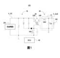
請參閱圖1為本揭露的隔離式轉換器的電路方塊圖。隔離式轉換器400可耦接前級電路200與負載300,且前級電路200可以為交流/直流轉換器、功率因數校正器、直流源等直流電源供應者。隔離式轉換器400包括初級側電路1B、變壓器2B、次級側電路3B及控制器4B,且變壓器2B包括初級側線圈22B與次級側線圈24B。值得一提,於一實施例中,隔離式轉換器400例如但不限於,可以由圖1所示的返馳式轉換器所構成,但並不以此為限。因此,舉凡具有變壓器2B對初級側與次級側進行隔離的轉換電路,皆應包含在本實施例之範疇當中。Please refer to FIG. 1 for a circuit block diagram of the isolated converter disclosed herein. The isolated
初級側電路1B包括開關SW,且次級側電路3B包括次級整流電路Cr。次級整流電路Cr可包括整流開關SWr與輸出電容Co,且整流開關SWr可選擇替換為被動式二極體。一般而言,控制器MUC通過控制開關SW與次級整流電路Cr來使變壓器2B儲能/釋能,以通過變壓器2B的儲能/釋能而將隔離式轉換器400所接收的直流電源V_DC轉換為輔助電源V_AUX。變壓器2B的初級側線圈22B與次級側線圈24B可形成平板型變壓器,以利於配置於電路板之中,於後文會有更進一步的說明,在此不再加以贅述。值得一提,於一實施例中,初級側電路1B與次級側電路3B的電路結構僅為示意性的範例,舉凡可構成隔離式轉換器400架構的初級側電路1B與次級側電路3B,皆應包含在本實施例之範疇當中。The
請參閱圖2A為本揭露的電路板的立體電路結構分解圖、圖2B為本揭露的電路板的立體電路結構組合圖,復配合參閱圖1。變壓器2B配置於電路板CB2,且初級側電路1B、次級側電路3B及控制器4B可配置於主電路板CB_M2。變壓器2B的初級側線圈22B與次級側線圈24B皆為平面化(planar)的走線結構,且形成於電路板CB2上,使鐵芯C2通過直接地套設於電路板CB2的初級側線圈22B與次級側線圈24B上而形成變壓器2B。其中,鐵芯C2包括鐵芯柱C22,且鐵芯柱C22通過鐵芯C2直接地套設於電路板CB2而穿設於電路板CB2的穿孔H4。由於變壓器2B未有傳統繞置線圈的繞線架,所有的走線皆形成於電路板CB2,因此變壓器2B為平面化結構而形成平板型變壓器。由於平板型變壓器較為平面,因此使得電路板CB2的高度較小。如此,電路板CB2可通過插接的的方式插接於主電路板CB_M2上而形成圖1的電路結構,以節省主電路板CB_M2的使用空間,但並不排除電路板CB2可形成或配置於主電路板CB_M2其中一區塊的實施方式。Please refer to FIG. 2A for a three-dimensional circuit structure exploded view of the circuit board disclosed in the present invention, and FIG. 2B for a three-dimensional circuit structure assembly view of the circuit board disclosed in the present invention, and refer to FIG. 1 in conjunction. The
因此,本揭露的隔離式轉換器400結構主要係將變壓器2B的初級側線圈22B與次級側線圈24B形成於電路板CB2上,而使得平板型變壓器能夠平面化(planar),以大幅度的提高隔離式轉換器400的空間利用率而達到高功率密度需求。並且,隔離式轉換器400也因使用平板型變壓器而具有體積小的特性,相對的可大幅提高隔離式轉換器400的操作頻率,因此開關SW與次級整流電路Cr的整流開關SWr可使用寬能隙(WBG)等第三代半導體元件作為主要功率開關,使隔離式轉換器400具有更高的效率、顯著縮減功率開關尺寸、更輕盈和改善散熱性能等優越性。Therefore, the structure of the isolated
請參閱圖3A為本揭露的變壓器線圈電路圖、圖3B為本揭露的變壓器走線配置方式示意圖,復配合參閱圖1~2B。在圖3A中,變壓器2B包括初級側與次級側。初級側包括初級側線圈22B,且次級側包括次級側線圈24B。變壓器2B還可以選擇性的包括輔助線圈W1、W2、W3、W4、W5,且輔助線圈W5可與次級側線圈24B形成中心抽頭式的線圈結構。其中,輔助線圈W1、W2、W3、W4、W5可通過耦合的方式,耦合由初級側線圈22B所提供的能量,且可通過調整其圈數來調整耦合而得的電壓。進一步而言,輔助線圈W1、W2、W3、W4、W5可作為偵測、輔助電源、對負載300供電等之用,主要是用以提供不同輸出電壓的需求。值得一提,於一實施例中,輔助線圈W1、W2、W3、W4、W5的數量及其結構特徵(獨立式或中心抽頭式等),僅為示意性的範例,並不以圖3A為限。Please refer to FIG. 3A for the transformer coil circuit diagram disclosed herein, and FIG. 3B for the transformer wiring configuration diagram disclosed herein, and refer to FIG. 1 to FIG. 2B in combination. In FIG. 3A , the
配合參閱圖3B為電路板CD的剖面示意圖,為求著重於本揭露的主要特徵,其剖面位置僅出示變壓器2B的區塊。在圖3B中,電路板CB2為多層板(在此以6層板為例,但不以此為限)。電路板CB2包括複數初級層LP與複數次級層LS,且遠離中心線X的二側分別為電路板CB2的頂層與底層。複數條初級側走線Tp2分別形成於電路板CB2的初級層LP,且每層初級層LP至少包括一條環繞數圈的初級側走線Tp2(圖3B以四層初級層LP表示,但不以此為限)。初級側走線Tp2可通過各個初級層LP的聯通(例如使用過孔,圖未示)而使初級側走線Tp2串接在一起,以作為耦接初級側電路1B的初級側線圈22B。Referring to FIG. 3B , which is a cross-sectional schematic diagram of a circuit board CD, in order to focus on the main features of the present disclosure, the cross-sectional position only shows the block of the
複數條次級側走線Ts2分別形成於電路板CB2的次級層LS,且每層次級層LS至少包括一條繞數圈的次級側走線Ts2(圖3B以二層次級層LS表示,但不以此為限)。次級側走線Ts2可通過各個次級層LS的聯通(例如使用過孔,圖未示)而使次級側走線Ts2串接在一起,以作為耦接次級側電路3B的次級側線圈24B。值得一提,於一實施例中,各層板所形成的走線的材質可以為銅箔,但並不排除可以使用易於導電的其他金屬箔(例如但不限於,金、銀等)。A plurality of secondary side traces Ts2 are formed on the secondary layer LS of the circuit board CB2, and each secondary layer LS includes at least one secondary side trace Ts2 with multiple turns (Fig. 3B shows two layers of secondary layer LS, but not limited thereto). The secondary side traces Ts2 can be connected in series through the interconnection of each secondary layer LS (for example, by using vias, not shown) to serve as a
鐵芯C2環繞於電路板CB2,且鐵芯C2包括鐵芯柱C22。鐵芯柱C22貫穿電路板CB2的穿孔H4,使初級側走線Tp2與次級側走線Ts2環繞於穿孔H4,且於鐵芯C2套設於初級側走線Tp2與次級側走線Ts2後,可形成閉合磁路而構成變壓器2B。進一步而言,如圖3B所示,變壓器2B的形成方法為初級側走線Tp2接近該電路板的中心(即中心線X),且次級側走線Ts2相對於初級側走線Tp2而遠離中心,以形成三明治走線。The iron core C2 surrounds the circuit board CB2, and the iron core C2 includes an iron core column C22. The iron core column C22 passes through the through hole H4 of the circuit board CB2, so that the primary side trace Tp2 and the secondary side trace Ts2 surround the through hole H4, and after the iron core C2 is sleeved on the primary side trace Tp2 and the secondary side trace Ts2, a closed magnetic circuit can be formed to form a
意即,初級側走線Tp2形成在電路板CB2中較為中心的位置,且次級側走線Ts2形成在電路板CB2接近頂層或底層的位置。如此,可以減小變壓器2B的漏感,提高隔離式轉換器400的效率。值得一提,於一實施例中,變壓器2B的走線設計,並不以三明治走線為限。具體而言,若不採用三明治走線的設計(例如但不限於,初級層LP配置於接近頂層,且次級層LS配置於接近底層),則可降初級層LP與次級層LS之間的耦合電容,降低變壓器2B運作時的雜訊。That is, the primary side trace Tp2 is formed at a relatively central position in the circuit board CB2, and the secondary side trace Ts2 is formed at a position close to the top layer or the bottom layer of the circuit board CB2. In this way, the leakage inductance of the
另外一方面,次級層LS與初級層LP分別包括彼此相鄰的次級相鄰層LSa與初級相鄰層LPa。輔助走線Cf1、Cf2、Cf3、Cf4分別形成於電路板CB2的初級相鄰層LPa,且初級相鄰層LPa可包括至少一條輔助走線Cf1、Cf2、Cf3、Cf4。輔助走線Cf1、Cf2、Cf3、Cf4可配置於單層的初級相鄰層LPa而形成輔助線圈W1、W2、W3、W4,也可通過各個初級相鄰層LPa的聯通(例如使用過孔,圖未示)而使相同路徑的輔助走線Cf1、Cf2、Cf3、Cf4串接在一起,以作為輔助線圈W1、W2、W3、W4。On the other hand, the secondary layer LS and the primary layer LP respectively include a secondary adjacent layer LSa and a primary adjacent layer LPa adjacent to each other. Auxiliary traces Cf1, Cf2, Cf3, Cf4 are respectively formed in the primary adjacent layer LPa of the circuit board CB2, and the primary adjacent layer LPa may include at least one auxiliary trace Cf1, Cf2, Cf3, Cf4. Auxiliary traces Cf1, Cf2, Cf3, Cf4 can be arranged in a single-layer primary adjacent layer LPa to form auxiliary coils W1, W2, W3, W4, or auxiliary traces Cf1, Cf2, Cf3, Cf4 of the same path can be connected in series through the interconnection of each primary adjacent layer LPa (for example, using vias, not shown) to form auxiliary coils W1, W2, W3, W4.
相似地,輔助走線Cf5可形成於電路板CB2的次級相鄰層LSa,且次級相鄰層LSa可包括至少一條輔助走線Cf5。輔助走線Cf5可配置於單層的次級相鄰層LSa而形成輔助線圈W5,也可通過各個次級相鄰層LSa的聯通(例如使用過孔,圖未示)而使相同路徑的輔助走線Cf5串接在一起,以作為輔助線圈W5。此外,當次級層LS與初級層LP的層數各為1時(即電路板CB2為雙層板,且包括頂層及底層),則次級層LS即為次級相鄰層LSa,且初級層LP即為初級相鄰層LPa。次級相鄰層LSa包括一條環繞穿孔H4數圈的次級側走線Ts2與一條輔助走線Cf5,初級相鄰層LPa包括一條環繞穿孔H4數圈的初級側走線Tp2與至少一條輔助走線Cf1、Cf2、Cf3、Cf4。因此,當電路板CB2為雙層板時,其結構與可達成的功效可由本揭露的圖1~3B及其相應的段落描述而推知,在此不再加以贅述。Similarly, the auxiliary trace Cf5 can be formed in the secondary adjacent layer LSa of the circuit board CB2, and the secondary adjacent layer LSa can include at least one auxiliary trace Cf5. The auxiliary trace Cf5 can be arranged in a single layer of the secondary adjacent layer LSa to form an auxiliary coil W5, or the auxiliary traces Cf5 of the same path can be connected in series through the interconnection of each secondary adjacent layer LSa (for example, using vias, not shown) to form an auxiliary coil W5. In addition, when the number of layers of the secondary layer LS and the primary layer LP is 1 each (i.e., the circuit board CB2 is a double-layer board and includes a top layer and a bottom layer), the secondary layer LS is the secondary adjacent layer LSa, and the primary layer LP is the primary adjacent layer LPa. The secondary adjacent layer LSa includes a secondary side trace Ts2 that loops around the through hole H4 several times and an auxiliary trace Cf5, and the primary adjacent layer LPa includes a primary side trace Tp2 that loops around the through hole H4 several times and at least one auxiliary trace Cf1, Cf2, Cf3, Cf4. Therefore, when the circuit board CB2 is a double-layer board, its structure and achievable effects can be inferred from FIGS. 1 to 3B and the corresponding paragraphs of the present disclosure, and will not be elaborated here.
其中,輔助走線Cf1、Cf2、Cf3、Cf4、Cf5可依據後端的電路所需求的電壓大小,選擇性的調整環繞於穿孔H4的圈數。因此,輔助走線Cf1、Cf2、Cf3、Cf4與初級側走線Tp2可呈同心結構(中心為穿孔H4),且輔助走線Cf5與次級側走線Ts2可呈同心結構(中心為穿孔H4)。值得一提,於一實施例中,上述內文所述的過孔,其內部通常可填充導電材料(例如但不限於錫糕等用於導電的材料) ,以使變壓器2B的走線可通過過孔來電性連接。Among them, the auxiliary traces Cf1, Cf2, Cf3, Cf4, and Cf5 can selectively adjust the number of turns around the through hole H4 according to the voltage required by the circuit at the rear end. Therefore, the auxiliary traces Cf1, Cf2, Cf3, and Cf4 can be concentric with the primary trace Tp2 (with the through hole H4 at the center), and the auxiliary trace Cf5 can be concentric with the secondary trace Ts2 (with the through hole H4 at the center). It is worth mentioning that in one embodiment, the vias described in the above text can usually be filled with conductive materials (such as but not limited to conductive materials such as solder cakes) so that the traces of the
復參閱圖3B,在次級相鄰層LSa的次級側走線Ts2具有第一寬度Wh1、Wh3,且在初級相鄰層LPa的初級側走線Tp2具有第二寬度Wh2、Wh4。具體而言,在次級相鄰層LSa中,由最遠離穿孔H4的次級側走線Ts2至最接近穿孔H4的次級側走線Ts2的距離為第一寬度Wh1、Wh3。在初級相鄰層LPa中,由最遠離穿孔H4的初級側走線Tp2至最接近穿孔H4的初級側走線Tp2的距離為第二寬度Wh2、Wh4。而且,所述”寬度”可以為電路板CB2垂直於中心線X的任意截面中,該層走線所形成的最大距離(即由最遠離穿孔H4的走線至最接近穿孔H4的走線的距離)。在一實施例中,第一寬度Wh1、Wh3大於第二寬度Wh2、Wh4,可以使初級線圈Wp與次級線圈Ws耦合性更好,使次級線圈Ws感應而得的電壓更穩定。意即,在接近頂層的次級相鄰層LSa中,次級相鄰層LSa的次級側走線Ts2所形成的第一寬度Wh1較佳可涵蓋初級相鄰層LPa的初級側走線Tp2所形成的第二寬度Wh2,因此次級相鄰層LSa的次級側走線Ts2所形成的面積可大於初級相鄰層LPa的初級側走線Tp2所形成的面積。Referring again to FIG. 3B , the secondary side trace Ts2 in the secondary adjacent layer LSa has a first width Wh1, Wh3, and the primary side trace Tp2 in the primary adjacent layer LPa has a second width Wh2, Wh4. Specifically, in the secondary adjacent layer LSa, the distance from the secondary side trace Ts2 farthest from the through hole H4 to the secondary side trace Ts2 closest to the through hole H4 is the first width Wh1, Wh3. In the primary adjacent layer LPa, the distance from the primary side trace Tp2 farthest from the through hole H4 to the primary side trace Tp2 closest to the through hole H4 is the second width Wh2, Wh4. Moreover, the "width" can be the maximum distance formed by the routing of this layer in any cross section of the circuit board CB2 perpendicular to the center line X (i.e., the distance from the routing farthest from the through hole H4 to the routing closest to the through hole H4). In one embodiment, the first width Wh1, Wh3 is greater than the second width Wh2, Wh4, which can make the coupling between the primary coil Wp and the secondary coil Ws better, and make the voltage induced by the secondary coil Ws more stable. That is, in the secondary adjacent layer LSa close to the top layer, the first width Wh1 formed by the secondary side trace Ts2 of the secondary adjacent layer LSa can better cover the second width Wh2 formed by the primary side trace Tp2 of the primary adjacent layer LPa, so the area formed by the secondary side trace Ts2 of the secondary adjacent layer LSa can be larger than the area formed by the primary side trace Tp2 of the primary adjacent layer LPa.
此外,當初級相鄰層LPa包括的初級側走線Tp2與輔助走線Cf1、Cf2、Cf3、Cf4時,第二寬度Wh2、Wh4由輔助走線Cf1、Cf2、Cf3、Cf4與初級側走線Tp2形成。意即,次級相鄰層LSa的次級側走線Ts2所形成的第一寬度Wh1較佳可大於等於初級相鄰層LPa的初級側走線Tp2與輔助走線Cf1、Cf2、Cf3、Cf4所形成的第二寬度Wh2。其中,在初級相鄰層LPa中,由最遠離穿孔H4的走線(可以是初級側走線Tp2或輔助走線Cf1、Cf2、Cf3、Cf4的其中一者)至最接近穿孔H4的走線(可以是初級側走線Tp2或輔助走線Cf1、Cf2、Cf3、Cf4的另一者)的距離為第二寬度Wh2、Wh4。如此,可以使初級線圈Wp、次級線圈Ws及輔助線圈W1、W2、W3、W4、W5耦合性更好,使各線圈感應而得的電壓更穩定。In addition, when the primary adjacent layer LPa includes the primary side trace Tp2 and the auxiliary traces Cf1, Cf2, Cf3, Cf4, the second widths Wh2 and Wh4 are formed by the auxiliary traces Cf1, Cf2, Cf3, Cf4 and the primary side trace Tp2. That is, the first width Wh1 formed by the secondary side trace Ts2 of the secondary adjacent layer LSa is preferably greater than or equal to the second width Wh2 formed by the primary side trace Tp2 of the primary adjacent layer LPa and the auxiliary traces Cf1, Cf2, Cf3, Cf4. Among them, in the primary adjacent layer LPa, the distance from the routing farthest from the through hole H4 (which can be the primary side routing Tp2 or one of the auxiliary routings Cf1, Cf2, Cf3, Cf4) to the routing closest to the through hole H4 (which can be the primary side routing Tp2 or the other of the auxiliary routings Cf1, Cf2, Cf3, Cf4) is the second width Wh2, Wh4. In this way, the coupling of the primary coil Wp, the secondary coil Ws and the auxiliary coils W1, W2, W3, W4, W5 can be better, making the voltage sensed by each coil more stable.
值得一提,於一實施例中,第一寬度Wh3與第二寬度Wh4的相應關係同於第一寬度Wh1與第二寬度Wh2,在此不再加以贅述。此外,輔助走線Cf1、Cf2、Cf3、Cf4、Cf5較佳可配置於次級相鄰層LSa與初級相鄰層LPa,以提供較佳的耦合效果,但不以此為限。換言之,輔助走線Cf1、Cf2、Cf3、Cf4、Cf5可配置於次級層LS與初級層LP任意一者,只要可通過耦合而取得合適的電壓即可實施。It is worth mentioning that, in one embodiment, the corresponding relationship between the first width Wh3 and the second width Wh4 is the same as that between the first width Wh1 and the second width Wh2, and will not be described in detail here. In addition, the auxiliary traces Cf1, Cf2, Cf3, Cf4, and Cf5 are preferably arranged in the secondary adjacent layer LSa and the primary adjacent layer LPa to provide a better coupling effect, but are not limited thereto. In other words, the auxiliary traces Cf1, Cf2, Cf3, Cf4, and Cf5 can be arranged in any one of the secondary layer LS and the primary layer LP, as long as a suitable voltage can be obtained through coupling.
復參閱圖3B,鐵芯C2可包括氣隙gap,以通過氣隙gap配置來增加磁阻,避免變壓器2B在工作中產生磁飽和。其中,氣隙gap通常可形成於鐵芯柱C22,但氣隙gap形狀及氣隙gap位置,其可依照設計者的需求而定,因此並不以圖3B為限。其中,氣隙具有第一距離Y1,且初級側走線Tp2、次級側走線Ts2與穿孔H4具有複數個第二距離Y2,第二距離Y2係分別大於等於第一距離Y1的三倍。具體而言,由於走線與氣隙gap保持特定距離可以降低變壓器2B的切割損,且提升效率。因此,將次級側走線Ts2與穿孔H4的距離設定為氣隙gap的三倍為較佳的實施方式。Referring again to FIG. 3B , the core C2 may include an air gap to increase magnetic resistance through the configuration of the air gap to prevent the
另外一方面,由於本揭露的變壓器2B係於電路板CB2形成走線,因此可通過簡單的電路板CB2設計軟體即可調整電路板CB2各層的初級側走線Tp2、次級側走線Ts2與穿孔H4的距離。因此,相較於傳統的變壓器僅能在鐵芯C2上磨氣隙而無法調整線圈距離,本揭露變壓器2B使用形成於電路板CB2的走線結構,可達成有利於微調第二距離Y2之功效。此外,輔助走線Cf1、Cf2、Cf3、Cf4、Cf5較佳也可與穿孔H4之間具有第三距離,且第三距離大於等於第一距離Y1的三倍為較佳的實施方式。On the other hand, since the
請參閱圖4為本揭露的初級相鄰層的走線配置示意圖,復配合參閱圖1~3B。在圖4中,係示意接近電路板CB2頂層的初級相鄰層LPa的走線配置,其配置包括了初級側走線Tp2與輔助走線Cf1。如圖4所示,輔助走線Cf1可通過分數圈(即該層的走線環繞於穿孔H4的圈數非為整數圈)的配置方式,使變壓器2B得以微調所獲取的電壓,以達應用性更佳之需求。具體而言,為了更為穩定並精調輸出電壓的電壓值,變壓器2B可通過額外配置半圈(即輔助走線Cf1額外配置半圈)、1/4圈,甚至1/10圈等走線來微調輔助走線Cf1感應所獲得的電壓(以圖4為例,輔助走線Cf1為2.5圈),使其電壓能夠更為精準(例如但不限於12V等)。值得一提,於一實施例中,雖在圖4中僅出示輔助走線Cf1環繞於穿孔H4的圈數非為整數圈,然相似的初級側走線Tp2、級側走線Tsf及輔助走線Cf2、Cf3、Cf4、Cf5也可以通過分數圈的方式來微調所感應而得的電壓,在此不再加以贅述。Please refer to FIG. 4 for a schematic diagram of the wiring configuration of the primary adjacent layer disclosed in the present invention, and refer to FIG. 1 to FIG. 3B in conjunction. FIG. 4 shows the wiring configuration of the primary adjacent layer LPa close to the top layer of the circuit board CB2, which includes the primary side wiring Tp2 and the auxiliary wiring Cf1. As shown in FIG. 4, the auxiliary wiring Cf1 can be configured in a fractional circle (i.e., the number of circles of the wiring of this layer around the through hole H4 is not an integer), so that the
惟,以上所述,僅為本發明較佳具體實施例之詳細說明與圖式,惟本發明之特徵並不侷限於此,並非用以限制本發明,本發明之所有範圍應以下述之申請專利範圍為準,凡合於本發明申請專利範圍之精神與其類似變化之實施例,皆應包括於本發明之範疇中,任何熟悉該項技藝者在本發明之領域內,可輕易思及之變化或修飾皆可涵蓋在以下本案之專利範圍。However, the above description is only a detailed description and drawings of the preferred specific embodiments of the present invention, but the features of the present invention are not limited thereto, and are not used to limit the present invention. The entire scope of the present invention shall be subject to the following patent application scope. All embodiments that conform to the spirit of the patent application scope of the present invention and its similar variations shall be included in the scope of the present invention. Any changes or modifications that can be easily thought of by anyone familiar with the art within the field of the present invention can be covered by the following patent scope of this case.
400:隔離式轉換器 1B:初級側電路 SW:開關 2B:變壓器 22B:初級側線圈 24B:次級側線圈 W1、W2、W3、W4、W5:輔助線圈 3B:次級側電路 Cr:次級整流電路 SWr:整流開關 Co:輸出電容 4B:控制器 CB2:電路板 LP:初級層 LPa:初級相鄰層 Tp2:初級側走線 LS:次級層 LSa:次級相鄰層 Ts2:次級側走線 Cf1、Cf2、Cf3、Cf4、Cf5:輔助走線 H4:穿孔 CB_M2:主電路板 C2:鐵芯 C22:鐵芯柱 gap:氣隙 200:前級電路 300:負載 V_DC:直流電源 V_AUX:輔助電源 X:中心線 Wh1、Wh3:第一寬度 Wh2、Wh4:第二寬度 Y1:第一距離 Y2:第二距離 Y3:第三距離400:
圖1為本揭露的隔離式轉換器的電路方塊圖;FIG1 is a circuit block diagram of an isolated converter disclosed herein;
圖2A為本揭露的電路板的立體電路結構分解圖;FIG. 2A is a three-dimensional circuit structure exploded view of the circuit board disclosed in the present invention;
圖2B為本揭露的電路板的立體電路結構組合圖;FIG. 2B is a three-dimensional circuit structure assembly diagram of the circuit board disclosed herein;
圖3A為本揭露的變壓器線圈電路圖;FIG3A is a transformer coil circuit diagram of the present disclosure;
圖3B為本揭露的變壓器走線配置方式示意圖;及FIG3B is a schematic diagram of the transformer wiring configuration of the present disclosure; and
圖4為本揭露的初級相鄰層的走線配置示意圖。FIG. 4 is a schematic diagram of the wiring arrangement of the primary adjacent layer of the present disclosure.
2B:變壓器2B: Transformer
CB2:電路板CB2: Circuit board
LP:初級層LP: Primary level
LPa:初級相鄰層LPa: primary adjacent layer
Tp2:初級側走線Tp2: Beginner side routing
LS:次級層LS: Secondary layer
LSa:次級相鄰層LSa: Secondary neighbor layer
Ts2:次級側走線Ts2: Secondary side routing
Cf1、Cf2、Cf3、Cf4、Cf5:輔助走線Cf1, Cf2, Cf3, Cf4, Cf5: auxiliary routing
H4:穿孔H4: Perforation
C2:鐵芯C2: Iron core
C22:鐵芯柱C22: Iron core column
gap:氣隙gap: air gap
X:中心線X: Center line
Wh1、Wh3:第一寬度Wh1, Wh3: First width
Wh2、Wh4:第二寬度Wh2, Wh4: second width
Y1:第一距離Y1: First distance
Y2:第二距離Y2: Second distance
Y3:第三距離Y3: The third distance
Claims (14)
Translated fromChineseApplications Claiming Priority (2)
| Application Number | Priority Date | Filing Date | Title |
|---|---|---|---|
| US202263425014P | 2022-11-14 | 2022-11-14 | |
| US63/425,014 | 2022-11-14 |
Publications (2)
| Publication Number | Publication Date |
|---|---|
| TW202420346Atrue TW202420346A (en) | 2024-05-16 |
| TWI891121B TWI891121B (en) | 2025-07-21 |
Family
ID=88833518
Family Applications (7)
| Application Number | Title | Priority Date | Filing Date |
|---|---|---|---|
| TW112143653ATWI891121B (en) | 2022-11-14 | 2023-11-13 | Planar transformer |
| TW112212259UTWM656161U (en) | 2022-11-14 | 2023-11-13 | Planar magnetic components |
| TW112143629ATWI890192B (en) | 2022-11-14 | 2023-11-13 | Planar transformer |
| TW112143628ATWI872803B (en) | 2022-11-14 | 2023-11-13 | Power supply unit and dc conversion module |
| TW112143654ATWI852831B (en) | 2022-11-14 | 2023-11-13 | Planar magnetic components |
| TW112143640ATWI879226B (en) | 2022-11-14 | 2023-11-13 | Planar magnetic components |
| TW114100115ATW202518826A (en) | 2022-11-14 | 2023-11-13 | Power supply unit |
Family Applications After (6)
| Application Number | Title | Priority Date | Filing Date |
|---|---|---|---|
| TW112212259UTWM656161U (en) | 2022-11-14 | 2023-11-13 | Planar magnetic components |
| TW112143629ATWI890192B (en) | 2022-11-14 | 2023-11-13 | Planar transformer |
| TW112143628ATWI872803B (en) | 2022-11-14 | 2023-11-13 | Power supply unit and dc conversion module |
| TW112143654ATWI852831B (en) | 2022-11-14 | 2023-11-13 | Planar magnetic components |
| TW112143640ATWI879226B (en) | 2022-11-14 | 2023-11-13 | Planar magnetic components |
| TW114100115ATW202518826A (en) | 2022-11-14 | 2023-11-13 | Power supply unit |
Country Status (4)
| Country | Link |
|---|---|
| US (5) | US20240162833A1 (en) |
| EP (5) | EP4369586A1 (en) |
| CN (6) | CN118039311A (en) |
| TW (7) | TWI891121B (en) |
Families Citing this family (2)
| Publication number | Priority date | Publication date | Assignee | Title |
|---|---|---|---|---|
| US20240072839A1 (en)* | 2022-08-30 | 2024-02-29 | Texas Instruments Incorporated | Differential electrical balance duplexers |
| US20250293594A1 (en)* | 2024-03-15 | 2025-09-18 | Delta Electronics, Inc. | Resonant converter |
Family Cites Families (26)
| Publication number | Priority date | Publication date | Assignee | Title |
|---|---|---|---|---|
| JP2002299130A (en)* | 2001-04-02 | 2002-10-11 | Densei Lambda Kk | Composite element for power source |
| JP5359749B2 (en)* | 2009-09-30 | 2013-12-04 | Tdk株式会社 | Transformer and switching power supply |
| CN101917053B (en)* | 2010-08-03 | 2012-10-24 | 浪潮电子信息产业股份有限公司 | Method for carrying out centralized power supply on RACK system |
| US9467054B2 (en)* | 2013-11-07 | 2016-10-11 | Futurewei Technologies, Inc. | Current sensing apparatus for resonant tank in an LLC resonant converter |
| CN105655113B (en)* | 2014-11-12 | 2018-04-17 | 台达电子工业股份有限公司 | PCB planar transformer and converter using same |
| CN106484045B (en)* | 2015-08-25 | 2020-06-30 | 佛山市顺德区顺达电脑厂有限公司 | Server |
| TWI542135B (en)* | 2015-09-11 | 2016-07-11 | 萬國半導體(開曼)股份有限公司 | Voltage converter |
| EP3282550B1 (en)* | 2016-02-05 | 2020-04-15 | Guangdong Oppo Mobile Telecommunications Corp., Ltd. | Adapter and charging control method |
| EP3440768B1 (en)* | 2016-04-06 | 2022-06-08 | Telefonaktiebolaget LM Ericsson (PUBL) | Power converter |
| CN106655721A (en)* | 2017-03-13 | 2017-05-10 | 杭州富特科技股份有限公司 | Power supply power module and circuit board combination thereof, and power converter |
| CN107818865B (en)* | 2017-09-19 | 2019-05-31 | 东南大学 | A kind of high frequency centre tap flat surface transformer in LLC half bridge resonant |
| TWI630628B (en)* | 2017-10-19 | 2018-07-21 | 光壽科技有限公司 | Capacitive resistance voltage conversion device |
| EP3629463A1 (en)* | 2018-09-27 | 2020-04-01 | Siemens Aktiengesellschaft | Resonant direct current regulator |
| CN109494749B (en)* | 2018-11-30 | 2021-03-26 | 华中科技大学 | A plug-and-play integrated modular series dynamic voltage compensator |
| CN111383830B (en)* | 2018-12-29 | 2021-05-28 | 台达电子企业管理(上海)有限公司 | Magnetic unit |
| CN109546872B (en)* | 2019-01-22 | 2023-09-15 | 东莞育嘉电子有限公司 | Power supply system capable of being infinitely extended through parallel superposition |
| US11848140B2 (en)* | 2019-06-11 | 2023-12-19 | Virginia Tech Intellectual Properties, Inc. | Integrated parallel matrix transformer and inductor |
| CN112564485B (en)* | 2019-09-10 | 2022-03-08 | 中车株洲电力机车研究所有限公司 | LLC resonant converter and control method thereof |
| CN111463879A (en)* | 2020-04-29 | 2020-07-28 | 恩益达电源科技(苏州)有限公司 | Power control system for charging pile |
| DE102020118708A1 (en)* | 2020-07-15 | 2022-01-20 | WAGO Verwaltungsgesellschaft mit beschränkter Haftung | ELECTRICAL ARRANGEMENT WITH TRANSFORMER FOR TRANSMITTING SIGNALS FROM A PRIMARY SIDE TO A SECONDARY SIDE |
| US12362772B2 (en)* | 2020-07-21 | 2025-07-15 | Omnifi Inc. | Flexible wireless interconnection and board diversity |
| US11594973B2 (en)* | 2020-08-04 | 2023-02-28 | Delta Electronics Inc. | Multiple-port bidirectional converter and control method thereof |
| TWM612250U (en)* | 2021-01-14 | 2021-05-21 | 台達電子工業股份有限公司 | Magnetic element |
| US20230162905A1 (en)* | 2021-02-08 | 2023-05-25 | Navitas Semiconductor Limited | Planar transformer including noise cancellation for auxiliary winding |
| US20230005659A1 (en)* | 2021-07-05 | 2023-01-05 | Navitas Semiconductor Limited | Systems and methods for improving winding losses in planar transformers |
| WO2024077528A1 (en)* | 2022-10-12 | 2024-04-18 | Innoscience (Shenzhen) Semiconductor Co., Ltd. | GaN-BASED SWITCHED-MODE POWER SUPPLY WITH PLANAR TRANSFORMER |
- 2023
- 2023-11-13EPEP23209486.2Apatent/EP4369586A1/enactivePending
- 2023-11-13EPEP23209562.0Apatent/EP4369365A1/enactivePending
- 2023-11-13CNCN202311504360.0Apatent/CN118039311A/enactivePending
- 2023-11-13CNCN202311504365.3Apatent/CN118041064A/enactivePending
- 2023-11-13USUS18/507,853patent/US20240162833A1/enactivePending
- 2023-11-13CNCN202323055274.4Upatent/CN221551625U/enactiveActive
- 2023-11-13EPEP23209405.2Apatent/EP4369363A3/enactivePending
- 2023-11-13CNCN202311506112.XApatent/CN118039314A/enactivePending
- 2023-11-13TWTW112143653Apatent/TWI891121B/enactive
- 2023-11-13TWTW112212259Upatent/TWM656161U/enunknown
- 2023-11-13USUS18/507,446patent/US20240161966A1/enactivePending
- 2023-11-13CNCN202311504363.4Apatent/CN118039313A/enactivePending
- 2023-11-13CNCN202311504362.XApatent/CN118039312A/enactivePending
- 2023-11-13TWTW112143629Apatent/TWI890192B/enactive
- 2023-11-13USUS18/507,694patent/US20240161967A1/enactivePending
- 2023-11-13EPEP23209566.1Apatent/EP4369366B1/enactiveActive
- 2023-11-13TWTW112143628Apatent/TWI872803B/enactive
- 2023-11-13TWTW112143654Apatent/TWI852831B/enactive
- 2023-11-13TWTW112143640Apatent/TWI879226B/enactive
- 2023-11-13TWTW114100115Apatent/TW202518826A/enunknown
- 2023-11-13EPEP23209485.4Apatent/EP4369364A1/enactivePending
- 2023-11-13USUS18/507,751patent/US20240161968A1/enactivePending
- 2023-11-13USUS18/507,775patent/US20240161969A1/enactivePending
Also Published As
| Publication number | Publication date |
|---|---|
| US20240161966A1 (en) | 2024-05-16 |
| EP4369366A1 (en) | 2024-05-15 |
| CN118039313A (en) | 2024-05-14 |
| CN221551625U (en) | 2024-08-16 |
| US20240161967A1 (en) | 2024-05-16 |
| TW202518826A (en) | 2025-05-01 |
| TW202420723A (en) | 2024-05-16 |
| CN118039311A (en) | 2024-05-14 |
| TWM656161U (en) | 2024-06-01 |
| TWI890192B (en) | 2025-07-11 |
| EP4369364A1 (en) | 2024-05-15 |
| US20240162833A1 (en) | 2024-05-16 |
| TW202427508A (en) | 2024-07-01 |
| CN118041064A (en) | 2024-05-14 |
| EP4369586A1 (en) | 2024-05-15 |
| EP4369363A2 (en) | 2024-05-15 |
| TWI872803B (en) | 2025-02-11 |
| EP4369363A3 (en) | 2024-07-10 |
| US20240161968A1 (en) | 2024-05-16 |
| TWI891121B (en) | 2025-07-21 |
| CN118039312A (en) | 2024-05-14 |
| TWI852831B (en) | 2024-08-11 |
| EP4369365A1 (en) | 2024-05-15 |
| US20240161969A1 (en) | 2024-05-16 |
| EP4369366B1 (en) | 2025-04-09 |
| TWI879226B (en) | 2025-04-01 |
| CN118039314A (en) | 2024-05-14 |
| TW202420345A (en) | 2024-05-16 |
| TW202429494A (en) | 2024-07-16 |
Similar Documents
| Publication | Publication Date | Title |
|---|---|---|
| TW202420346A (en) | Planar transformer | |
| US7671713B2 (en) | Integrated structure of passive elements in LLC resonance converter realized by flexible circuit boards | |
| CN104934209B (en) | The 3D integrated architectures of UHF Power converter | |
| CN216980294U (en) | A multi-layer winding planar transformer | |
| TWM556398U (en) | PCB type transformer and its coil board | |
| US11489449B2 (en) | Adjustable leakage inductance transformer | |
| CN217769886U (en) | Magnetic integrated assembly, resonant converter and power supply | |
| CN204792387U (en) | Hyperfrequency power converter's integrated framework of 3D | |
| CN216287941U (en) | Planar transformer or planar inductor | |
| TWI744104B (en) | Inductor | |
| CN118299162B (en) | A quadrature flux core structure for improving the power density of Sigma converters | |
| CN111614233A (en) | Dual input with current sharing and voltage sharing inductor LLC resonant half-bridge circuit type planar transformer | |
| CN223038743U (en) | Integrated magnetic element and switching power supply | |
| CN115050569A (en) | Optimization method of low-loss magnetic integration planar transformer for LLC resonant converter | |
| CN202796402U (en) | transformer | |
| CN114520091A (en) | inductance | |
| CN114944273A (en) | Magnetic integrated resonance power transformer | |
| CN113764173A (en) | Planar transformer structure of integrated Y capacitor |