TW202417895A - Display device and electronic apparatus - Google Patents
Display device and electronic apparatusDownload PDFInfo
- Publication number
- TW202417895A TW202417895ATW112132712ATW112132712ATW202417895ATW 202417895 ATW202417895 ATW 202417895ATW 112132712 ATW112132712 ATW 112132712ATW 112132712 ATW112132712 ATW 112132712ATW 202417895 ATW202417895 ATW 202417895A
- Authority
- TW
- Taiwan
- Prior art keywords
- layer
- diamond
- light
- organic
- display device
- Prior art date
Links
Images


Classifications
- H—ELECTRICITY
- H10—SEMICONDUCTOR DEVICES; ELECTRIC SOLID-STATE DEVICES NOT OTHERWISE PROVIDED FOR
- H10K—ORGANIC ELECTRIC SOLID-STATE DEVICES
- H10K85/00—Organic materials used in the body or electrodes of devices covered by this subclass
- H10K85/60—Organic compounds having low molecular weight
- H10K85/615—Polycyclic condensed aromatic hydrocarbons, e.g. anthracene
- H—ELECTRICITY
- H10—SEMICONDUCTOR DEVICES; ELECTRIC SOLID-STATE DEVICES NOT OTHERWISE PROVIDED FOR
- H10K—ORGANIC ELECTRIC SOLID-STATE DEVICES
- H10K85/00—Organic materials used in the body or electrodes of devices covered by this subclass
- H10K85/60—Organic compounds having low molecular weight
- H—ELECTRICITY
- H10—SEMICONDUCTOR DEVICES; ELECTRIC SOLID-STATE DEVICES NOT OTHERWISE PROVIDED FOR
- H10K—ORGANIC ELECTRIC SOLID-STATE DEVICES
- H10K50/00—Organic light-emitting devices
- H10K50/10—OLEDs or polymer light-emitting diodes [PLED]
- H10K50/11—OLEDs or polymer light-emitting diodes [PLED] characterised by the electroluminescent [EL] layers
- H10K50/115—OLEDs or polymer light-emitting diodes [PLED] characterised by the electroluminescent [EL] layers comprising active inorganic nanostructures, e.g. luminescent quantum dots
- H—ELECTRICITY
- H10—SEMICONDUCTOR DEVICES; ELECTRIC SOLID-STATE DEVICES NOT OTHERWISE PROVIDED FOR
- H10K—ORGANIC ELECTRIC SOLID-STATE DEVICES
- H10K50/00—Organic light-emitting devices
- H10K50/10—OLEDs or polymer light-emitting diodes [PLED]
- H10K50/11—OLEDs or polymer light-emitting diodes [PLED] characterised by the electroluminescent [EL] layers
- H10K50/125—OLEDs or polymer light-emitting diodes [PLED] characterised by the electroluminescent [EL] layers specially adapted for multicolour light emission, e.g. for emitting white light
- H10K50/13—OLEDs or polymer light-emitting diodes [PLED] characterised by the electroluminescent [EL] layers specially adapted for multicolour light emission, e.g. for emitting white light comprising stacked EL layers within one EL unit
- H—ELECTRICITY
- H10—SEMICONDUCTOR DEVICES; ELECTRIC SOLID-STATE DEVICES NOT OTHERWISE PROVIDED FOR
- H10K—ORGANIC ELECTRIC SOLID-STATE DEVICES
- H10K50/00—Organic light-emitting devices
- H10K50/10—OLEDs or polymer light-emitting diodes [PLED]
- H10K50/14—Carrier transporting layers
- H10K50/16—Electron transporting layers
- H—ELECTRICITY
- H10—SEMICONDUCTOR DEVICES; ELECTRIC SOLID-STATE DEVICES NOT OTHERWISE PROVIDED FOR
- H10K—ORGANIC ELECTRIC SOLID-STATE DEVICES
- H10K50/00—Organic light-emitting devices
- H10K50/80—Constructional details
- H10K50/805—Electrodes
- H—ELECTRICITY
- H10—SEMICONDUCTOR DEVICES; ELECTRIC SOLID-STATE DEVICES NOT OTHERWISE PROVIDED FOR
- H10K—ORGANIC ELECTRIC SOLID-STATE DEVICES
- H10K59/00—Integrated devices, or assemblies of multiple devices, comprising at least one organic light-emitting element covered by group H10K50/00
- H10K59/10—OLED displays
- H10K59/12—Active-matrix OLED [AMOLED] displays
- H—ELECTRICITY
- H10—SEMICONDUCTOR DEVICES; ELECTRIC SOLID-STATE DEVICES NOT OTHERWISE PROVIDED FOR
- H10K—ORGANIC ELECTRIC SOLID-STATE DEVICES
- H10K85/00—Organic materials used in the body or electrodes of devices covered by this subclass
- H10K85/60—Organic compounds having low molecular weight
- H10K85/649—Aromatic compounds comprising a hetero atom
- H10K85/654—Aromatic compounds comprising a hetero atom comprising only nitrogen as heteroatom
- H—ELECTRICITY
- H10—SEMICONDUCTOR DEVICES; ELECTRIC SOLID-STATE DEVICES NOT OTHERWISE PROVIDED FOR
- H10K—ORGANIC ELECTRIC SOLID-STATE DEVICES
- H10K85/00—Organic materials used in the body or electrodes of devices covered by this subclass
- H10K85/60—Organic compounds having low molecular weight
- H10K85/649—Aromatic compounds comprising a hetero atom
- H10K85/657—Polycyclic condensed heteroaromatic hydrocarbons
- H10K85/6572—Polycyclic condensed heteroaromatic hydrocarbons comprising only nitrogen in the heteroaromatic polycondensed ring system, e.g. phenanthroline or carbazole
- H—ELECTRICITY
- H10—SEMICONDUCTOR DEVICES; ELECTRIC SOLID-STATE DEVICES NOT OTHERWISE PROVIDED FOR
- H10K—ORGANIC ELECTRIC SOLID-STATE DEVICES
- H10K50/00—Organic light-emitting devices
- H10K50/10—OLEDs or polymer light-emitting diodes [PLED]
- H10K50/14—Carrier transporting layers
- H10K50/15—Hole transporting layers
- H—ELECTRICITY
- H10—SEMICONDUCTOR DEVICES; ELECTRIC SOLID-STATE DEVICES NOT OTHERWISE PROVIDED FOR
- H10K—ORGANIC ELECTRIC SOLID-STATE DEVICES
- H10K50/00—Organic light-emitting devices
- H10K50/10—OLEDs or polymer light-emitting diodes [PLED]
- H10K50/17—Carrier injection layers
- H—ELECTRICITY
- H10—SEMICONDUCTOR DEVICES; ELECTRIC SOLID-STATE DEVICES NOT OTHERWISE PROVIDED FOR
- H10K—ORGANIC ELECTRIC SOLID-STATE DEVICES
- H10K50/00—Organic light-emitting devices
- H10K50/10—OLEDs or polymer light-emitting diodes [PLED]
- H10K50/18—Carrier blocking layers
- H—ELECTRICITY
- H10—SEMICONDUCTOR DEVICES; ELECTRIC SOLID-STATE DEVICES NOT OTHERWISE PROVIDED FOR
- H10K—ORGANIC ELECTRIC SOLID-STATE DEVICES
- H10K50/00—Organic light-emitting devices
- H10K50/10—OLEDs or polymer light-emitting diodes [PLED]
- H10K50/18—Carrier blocking layers
- H10K50/181—Electron blocking layers
- H—ELECTRICITY
- H10—SEMICONDUCTOR DEVICES; ELECTRIC SOLID-STATE DEVICES NOT OTHERWISE PROVIDED FOR
- H10K—ORGANIC ELECTRIC SOLID-STATE DEVICES
- H10K50/00—Organic light-emitting devices
- H10K50/10—OLEDs or polymer light-emitting diodes [PLED]
- H10K50/19—Tandem OLEDs
Landscapes
- Physics & Mathematics (AREA)
- Engineering & Computer Science (AREA)
- Chemical & Material Sciences (AREA)
- Spectroscopy & Molecular Physics (AREA)
- Materials Engineering (AREA)
- Optics & Photonics (AREA)
- Microelectronics & Electronic Packaging (AREA)
- Crystallography & Structural Chemistry (AREA)
- Inorganic Chemistry (AREA)
- Nanotechnology (AREA)
- Electroluminescent Light Sources (AREA)
- Devices For Indicating Variable Information By Combining Individual Elements (AREA)
Abstract
Description
Translated fromChinese本揭示係關於顯示裝置及電子機器。The present disclosure relates to display devices and electronic machines.
近年以來,對於由被稱為OLED(Organic Light Emitting Diode)有機EL(Electro-Luminescence)元件等構成的顯示面板(顯示裝置),能够迅速實現薄型輕量化。更且,更提案在如此顯示面板的背面設置致動器、振動板等,使面板本身振動而再生聲音的顯示面板。 [先前技術文獻] [專利文獻]In recent years, display panels (display devices) composed of organic EL (Electro-Luminescence) elements such as OLED (Organic Light Emitting Diode) have been rapidly becoming thinner and lighter. Furthermore, it has been proposed to provide an actuator, a vibration plate, etc. on the back of such a display panel so that the panel itself vibrates and reproduces sound.[Prior technical literature][Patent literature]
[專利文獻1]日本特開2022-62222號公報[Patent Document 1] Japanese Patent Application Publication No. 2022-62222
[發明欲解決之課題][Problems to be solved by the invention]
但是,在使面板本身振動而再生聲音的顯示面板(顯示裝置)中,存在在顯示影像中產生色斑的情况。However, in a display panel (display device) that reproduces sound by vibrating the panel itself, color unevenness may occur in a displayed image.
在此,在本揭示中,提案了能够抑制顯示影像的色斑的產生的顯示裝置及電子機器。 [為解決課題之手段]Here, in this disclosure, a display device and an electronic device capable of suppressing the generation of color spots in displayed images are proposed.[Means for solving the problem]
根據本發明,提供具備具有複數有機EL元件的顯示面板,和與前述顯示面板相接地設置,驅動前述顯示面板的驅動部,前述有機EL元件係包括由120℃以上的玻璃轉移點的高玻璃轉移溫度材料構成的有機層的顯示裝置。According to the present invention, a display device is provided that includes a display panel having a plurality of organic EL elements and a driving unit that is disposed in contact with the display panel and drives the display panel, wherein the organic EL elements include an organic layer composed of a high glass transition temperature material having a glass transition point of 120°C or higher.
又,根據本發明,為搭載顯示裝置的電子機器中,提供前述顯示裝置係具備具有複數有機EL元件的顯示面板,和與前述顯示面板相接地設置,驅動前述顯示面板的驅動部,前述有機EL元件係包括由120℃以上的玻璃轉移點的高玻璃轉移溫度材料構成的有機層的電子機器。Furthermore, according to the present invention, in an electronic device equipped with a display device, the display device is provided to include a display panel having a plurality of organic EL elements, and a driving unit provided in contact with the display panel to drive the display panel, wherein the organic EL element is an electronic device including an organic layer composed of a high glass transition temperature material having a glass transition point of 120°C or more.
以下,參照附加圖面,對於本揭示之適切實施形態詳細加以說明。 然而,在本說明書及圖面中,對於具有實質上相同的機能構成的構成要素,經由附加相同的符號而省略重複說明。又,在本說明書及圖面中,具有實質上相同或類似的機能構成的複數構成要素,有在相同的符號之後附加不同的字母來區別的情形。但是,在不需要特別區分具有實質上相同或類似的機能構成的複數構成要素的每一個的情況下,僅附上相同的符號。The following describes the appropriate implementation forms of the present disclosure in detail with reference to the attached drawings.However, in this specification and drawings, for components having substantially the same functional configuration, repeated descriptions are omitted by attaching the same symbols. In addition, in this specification and drawings, multiple components having substantially the same or similar functional configurations are distinguished by attaching different letters after the same symbols. However, when there is no need to specifically distinguish each of the multiple components having substantially the same or similar functional configurations, only the same symbols are attached.
然而,說明按照以下順序進行。 1.創作本揭示的實施形態的背景 1.1顯示器的概略構成 1.2背景 2.本揭示的實施形態的概略 3.第1之實施形態 4.第2之實施形態 5.第3之實施形態 6.第4之實施形態 7.第5之實施形態 8.第6之實施形態 9.總結 10.補足However, the description is given in the following order.1. Background of the implementation of the present disclosure1.1 Schematic structure of the display1.2 Background2. Overview of the implementation of the present disclosure3. The first implementation4. The second implementation5. The third implementation6. The fourth implementation7. The fifth implementation8. The sixth implementation9.
<<1. 創作本揭示的實施形態的背景>> <1.1 顯示器的概略構成> 首先,在說明本揭示的實施形態之前,作為對本發明人等創作本揭示的實施形態的背景的說明,參照圖1至圖5,說明顯示器(顯示裝置)1的概略構成。圖1係斜視地顯示本揭示的顯示器1的概略構成例圖,圖2係本揭示的顯示器1的電路構成例的電路圖,圖3係本揭示的顯示器1的畫素11的電路構成例的電路圖。圖4係顯示本揭示的顯示面板10的展開斜視構成例圖,圖5係顯示本揭示的系統電路基板40的機能方塊例圖。然而,顯示器1係相當於本揭示之「顯示裝置」之一具體例。<<1. Background of the implementation form of the present disclosure>><1.1 Schematic structure of the display>First, before explaining the implementation form of the present disclosure, as an explanation of the background of the implementation form of the present disclosure created by the inventors, the schematic structure of the display (display device) 1 is explained with reference to Figures 1 to 5. Figure 1 is a schematic structure example diagram of the
該顯示器1係使用被稱為OLED(Organic Light Emitting Diode)之有機(Electro-Luminescence)元件作為畫素的薄型自發光顯示器。The
顯示器1係例如具有具有顯示領域1A的顯示面板10、和保護顯示面板10的端緣(顯示領域1A的周緣)的框體20。更且,顯示器1係如圖2所示,例如具有驅動顯示面板10的系統電路基板40、和將顯示面板10和系統電路基板40電連接的印刷電路30。又,在顯示面板10的顯示領域1A中,複數畫素11配置成矩陣狀。然而,在本揭示中,系統電路基板40雖設置在顯示面板10的背面側,但在圖2中,為了方便,系統電路基板40係圖示在顯示面板10的旁邊。The
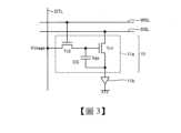
在圖3,顯示本揭示之監視器1之畫素11之電路構成例的電路圖。顯示面板10係例如具有延伸存在行方向的複數閘極線WSL及複數電源線DSL,以及延伸存在列方向的複數資料線DTL。對應於資料線DTL和閘極線WSL的交叉部分設置畫素11。各資料線DTL、各閘極線WSL及各電源線DSL係藉由印刷電路30,與系統電路基板40的輸出端電性連接。FIG3 shows a circuit diagram of a circuit configuration example of a
掃描線WSL係用於各畫素11的選擇,向各畫素11供給按特定的單位(例如畫素行)選擇各畫素11的選擇脈衝。信號線DTL係用於向各畫素11供給與影像信號對應的信號電壓(後述的信號電壓Vimage),向各畫素11供給包含信號電壓Vimage的資料脈衝。電源線DSL係向各畫素11供給電力。The scanning line WSL is used to select each
各畫素11係例如包含發出紅色光的畫素、發出綠色光的畫素、或者發出藍色光的畫素。然而,各畫素11係例如更可為發出其他顏色的光(例如白色光、黃色光等)的畫素。各畫素列中,例如,複數信號線DTL被1條1條分配。各畫素行中,例如,複數掃描線WSL被1條1條分配。各畫素行中,例如,複數電源線DSL被1條1條分配。Each
各畫素11係具有畫素電路11a、和有機EL元件11b。畫素電路11a係控制有機EL元件11b的發光・消滅。畫素電路11a係具有保持經由後述的信號寫入而寫入各畫素11的電壓(信號電壓Vimage)的機能。畫素電路11a係更具有向有機EL元件11b輸出與保持的電壓的大小對應的大小的驅動電流的機能。畫素電路11a係包含例如驅動電晶體Tr1、寫入電晶體Tr2及保持電容Cs。Each
寫入電晶體Tr2係控制對應驅動電晶體Tr1的閘極之影像信號相對應的信號電壓Vimage的施加。具體而言,寫入電晶體Tr2係對信號線DTL的電壓進行取樣的同時,將經由取樣得到的電壓寫入驅動電晶體Tr1的閘極。將經由取樣獲得的電壓寫入驅動電晶體Tr1的閘極稱為信號寫入。驅動電晶體Tr1係與有機EL元件11b串聯連接。驅動電晶體Tr1係驅動有機EL元件11b。驅動電晶體Tr1係根據由寫入電晶體Tr2取樣的電壓的大小,來控制流過有機EL元件11b的電流。保持電容Cs係能够在驅動電晶體Tr1的閘極-源極之間保持特定的電壓。保持電容Cs係具有在特定的期間內,將驅動電晶體Tr1的閘極-源極間電壓Vgs保持一定的作用。然而,畫素電路11a係可為對2Tr-1C的電路附加各種電容或電晶體的電路構成,或亦可為與2Tr-1C的電路構成不同的電路構成。The write transistor Tr2 controls the application of the signal voltage Vimage corresponding to the image signal to the gate of the corresponding drive transistor Tr1. Specifically, the write transistor Tr2 samples the voltage of the signal line DTL and writes the sampled voltage into the gate of the drive transistor Tr1. Writing the sampled voltage into the gate of the drive transistor Tr1 is called signal writing. The drive transistor Tr1 is connected in series with the
寫入電晶體Tr2的閘極係與掃描線WSL連接。寫入電晶體Tr2的源極或汲極係與信號線DTL連接。在寫入電晶體Tr2的源極及汲極中,未連接到信號線DTL的端子係連接到驅動電晶體Tr1的閘極。驅動電晶體Tr1的源極或汲極係與電源線DSL連接。在驅動電晶體Tr1的源極及汲極中,未連接到電源線DSL的端子係連接到有機EL元件11b的陽極。保持電容Cs的一端係連接到驅動電晶體Tr1的閘極。保持電容Cs的另一端係與驅動電晶體Tr1的源極及汲極中的有機EL元件11b側的端子連接。The gate of the write transistor Tr2 is connected to the scanning line WSL. The source or drain of the write transistor Tr2 is connected to the signal line DTL. Among the source and drain of the write transistor Tr2, the terminal not connected to the signal line DTL is connected to the gate of the drive transistor Tr1. The source or drain of the drive transistor Tr1 is connected to the power line DSL. Among the source and drain of the drive transistor Tr1, the terminal not connected to the power line DSL is connected to the anode of the
圖4中,顯示本揭示之顯示面板10之展開斜視構成例。顯示面板10係例如具有面板13、配置在面板13的背面側的散熱膜14、以及激振部308。此等面板13和散熱膜14係例如藉由黏著劑加以層積。又,激振部308係以藉由散熱膜14與面板13接觸的方式設置。又,在本揭示中,亦可不設置散熱膜14,此時,激振部308係以與面板13接觸的方式設置。FIG. 4 shows an example of the unfolded oblique structure of the
面板13係在基板上設置有包含複數畫素11配置成矩陣狀的顯示領域1A的框體領域1B的面板。例如,後述的激振部驅動電路49(參照圖5)係根據與聲音信號對應的信號電壓(後述的信號電壓Vsound),使激振部(激振器)308振動,將該振動傳遞給面板13。因此,面板13係可以用作平面揚聲器。又,在本揭示中,例如由致動器構成的激振部308係亦可在面板13的背面側設置1個或複數個。又,散熱膜14係將經由激振部308在面板13產生的熱,向外部散熱。The
圖5中,顯示本揭示的系統電路基板40的機能方塊例。例如,系統電路基板40的處理器42係可基於從外部輸入的信號,在顯示面板10上顯示影像。處理器42係可基於從外部輸入的信號的輸入操作命令,例如在顯示面板10上執行影像的頻道變更、音量增大、音量减小、靜音、節目表的顯示、影像放大、影像縮小及2畫面顯示中的任1者。FIG5 shows a functional block example of the
系統電路基板40係例如具有收訊電路41。收訊電路41係構成為與收訊的信號的種類對應。例如,在收訊電路41收訊電視廣播信號的情況下,收訊電路41係例如具有天線端子、數位調諧器及信號分離器(圖示省略)。The
天線端子係輸入由收訊天線收訊到的電視廣播信號的端子。數位調諧器係例如對輸入到天線端子的電視廣播信號進行處理,輸出與使用者的選擇頻道對應的特定的傳輸流。信號分離器係例如從由數位調諧器獲得的傳輸流,抽取對應於使用者選擇頻道的部分TS(Transport Stream),並將抽取的部分TS輸出到處理器42。The antenna terminal is a terminal for inputting the television broadcast signal received by the receiving antenna. The digital tuner processes the television broadcast signal input to the antenna terminal and outputs a specific transport stream corresponding to the user's selected channel. The signal separator extracts a partial TS (Transport Stream) corresponding to the user's selected channel from the transport stream obtained by the digital tuner and outputs the extracted partial TS to the
例如,在收訊電路41係經由網路線路收訊IP(網絡協定)信號的情況下,收訊電路41係經由網路線路收訊IP信號,對收訊到的IP信號,例如進行IP網路中的標準協定處理。收訊電路41係更從進行協定處理的信號中,抽取與使用者的選擇頻道對應的部分TS(Transport Stream),並將抽取出的部分TS輸出到處理器42。For example, when the receiving
收訊電路41係例如在從處理器42輸入與由檢測信號理電路51得到的檢測結果對應的操作命令的情況下,對從外部輸入的信號,進行與輸入的操作命令對應的處理。例如,操作命令係影像的頻道變更時。此時,收訊電路41係從由外部輸入的信號中,抽取與變更後的頻道對應的部分TS,並將抽取出的部分TS,輸出到處理器42。又,例如,操作命令係節目表的顯示時。此時,收訊電路41係從由外部輸入的信號中,抽取與節目表對應的部分TS,並將抽取出的部分TS,輸出到處理器42。又,例如,操作命令為2畫面顯示時。此時,收訊電路41係從由外部輸入的信號中,抽取與輸入到收訊電路41的控制信號中指定2頻道對應的部分TS,並將抽取出的部分TS輸出到處理器42。For example, when an operation command corresponding to the detection result obtained by the detection
系統電路基板40係更包含例如處理器42及記憶體43。處理器42係控制顯示器1的各部分的動作。處理器42係例如將由收訊電路41獲得的部分TS,存儲在記憶體43內,或者將從記憶體43讀出的部分TS,送訊到解碼器44。處理器42係例如從後述的表43A,讀出與從檢測信號處理電路51輸入的檢測結果對應的操作命令,並將讀出的操作命令送訊給收訊電路41、影像信號處理電路45或聲音信號處理電路48。The
記憶體43係例如進行顯示器1的設定資訊的存儲及資料管理。記憶體43係可以存儲例如由收訊電路41獲得的部分TS。The
系統電路基板40係更具有例如解碼器44、影像信號處理電路45、圖形生成電路46、OLED面板驅動電路47、聲音信號處理電路48、激振部驅動電路49以及檢測信號處理電路51。The
解碼器44係例如可以經由對由收訊電路41獲得的部分TS中包括的影像PES(Packetized Elementary Stream)封包執行解碼處理,來獲得影像資料。另外,解碼器44係例如可以經由對由收訊電路41獲得的部分TS中包含的聲音PES封包進行解碼處理,來獲得聲音資料。The
影像信號處理電路45及圖形生成電路46係例如根據需要對由解碼器44得到的影像資料進行多畫像處理、圖形資料的重疊處理等。The image
影像信號處理電路45係對影像資料進行特定的處理,將進行特定的處理的影像資料輸出到圖形生成電路46。影像信號處理電路45係例如在從處理器42輸入與由檢測信號處理電路51得到的檢測結果對應的操作指令的情況下,對影像資料進行與輸入的操作命令對應的處理。影像信號處理電路45係將根據從處理器42輸入的操作命令進行處理的影像資料,輸出到圖形生成電路46。The image
又,在本揭示的實施形態中,顯示器1係並不限定於圖1至圖5所示的形態,可以適當變形。Furthermore, in the embodiment of the present disclosure, the
<1.2 背景> 接著,參照圖6及圖7,說明本發明人等創作本揭示的實施形態的背景。圖6及圖7係為說明本揭示的實施形態的背景的說明圖。<1.2 Background>Next, referring to FIG. 6 and FIG. 7, the background of the implementation form of the present disclosure created by the inventors is described. FIG. 6 and FIG. 7 are explanatory diagrams for explaining the background of the implementation form of the present disclosure.
如先前所說明,在顯示器(顯示裝置)1中,設置在顯示面板的背面側,作為用於驅動顯示面板的各種驅動部,設置有激振部或系統電路等。詳細而言,如圖6所示,在具有複數有機EL元件的顯示面板100的背面側,設有使顯示面板振動的激振部308、控制顯示面板100的顯示的顯示控制部(Timing Controller: T-con)302。又,在顯示面板100的背面側,設置有對激振部308或顯示控制部302進行控制的主控制部304、對顯示面板100、激振部308、顯示控制部302、主控制部304等供給電源的電源供給部(電源)306。然而,激振部308、顯示控制部302、主控制部304以及電源供給部306係相當於驅動顯示面板100的本揭示的「驅動部」的一個具體例。As described above, in the display (display device) 1, an excitation unit or a system circuit is provided on the back side of the display panel as various drive units for driving the display panel. Specifically, as shown in FIG6, an
然後,如圖7所示,由於激振部308(振動源)的振動,在顯示面板100局部產生熱(例如50℃~60℃程度),在顯示面板100的整體上,有產生10℃程度的溫度差異之情形。然後,由於如此的溫度分佈,有在顯示面板100的顯示影像中產生色斑的情形。Then, as shown in FIG7 , due to the vibration of the excitation unit 308 (vibration source), heat (e.g., about 50° C. to 60° C.) is generated locally in the
又,同樣地,有經由除了激振部308以外的顯示控制部302(例如產生超過80℃的熱)、主控制部304(例如產生超過70℃的熱)、電源供給部306(例如產生超過80℃的熱)等,在顯示面板100局部產生熱,在顯示面板100的顯示影像中產生色斑的情形。Similarly, heat may be generated locally in the
詳細而言,經由激振部308等熱源或振動源(在此,將成為熱源的要素的總稱稱為熱源(振動源)300) 300,顯示面板100被局部加熱,顯示面板100上的一部分有機EL元件的有機材料的結晶狀態則發生變化。然而,經由改變結晶狀態,該有機材料的電子或電洞的導電特性則發生變化。其結果,由於一部分有機EL元件的導電特性發生變化,所以在顯示面板100的整體上,有機EL元件的特性產生差異,在顯示面板100的顯示影像中產生色斑。Specifically, the
因此,在以往技術中,如圖7所示,經由在顯示面板100的背面分散配置激振部308等,或者在顯示面板100的背面,設定例如由具有1mm以下的膜厚的石墨薄片或鋁薄片構成的散熱膜200,抑制熱擴散,色斑的產生。Therefore, in the prior art, as shown in FIG. 7 , an
但是,例如,在顯示面板100為厚的情況下,為了使顯示面板100振動,經由激振部308的輸出變大,更容易產生局部的加熱,有不能抑制色斑的產生的情形。即,即使採用以往技術,在抑制色斑的產生方面存在有局限。However, for example, when the
<<2. 本揭示之實施形態之概略>> 因此,本發明人鑒於如此的狀況,對使用了即使在高溫特性亦難以改變的耐熱性高的材料的有機EL元件進行研究,從而創作本揭示的實施形態。以下,對本揭示的實施形態的概要進行說明。<<2. Overview of the implementation form of the present disclosure>>Therefore, in view of such a situation, the inventors of the present invention have studied organic EL elements using highly heat-resistant materials whose characteristics are difficult to change even at high temperatures, and have created the implementation form of the present disclosure. The following is an overview of the implementation form of the present disclosure.
已知物質具有固體、液體、氣體之3種狀態,但亦存在相對於分子等規則排列的固體,分子等不規則排列的被稱為玻璃(非晶質、非晶)的狀態。當物質溫度升高時,物質從固體變為玻璃、液體和氣體。然後,關於物質成為玻璃狀態的溫度,稱為玻璃轉移點(Tg)。It is known that substances have three states: solid, liquid, and gas. However, there is also a state called glass (amorphous, non-crystalline) in which molecules are irregularly arranged, compared to solids in which molecules are regularly arranged. When the temperature of a substance increases, the substance changes from solid to glass, liquid, and gas. Then, the temperature at which a substance becomes a glass state is called the glass transition point (Tg).
在此,本發明人等對使用經由加熱難以改變結晶構造的材料、即玻璃轉移點高的材料作為有機EL元件的材料進行了檢討。根據本發明人等的檢討,在設想的使用時的溫度條件下使用各種材料研究有機EL元件的發光效率,結果顯示玻璃轉移點(Tg)為120℃以上的材料,則有機EL元件的發光效率不會惡化。Here, the inventors of the present invention have examined the use of materials whose crystal structures are difficult to change by heating, that is, materials with high glass transition points, as materials for organic EL elements. According to the inventors' examination, the luminous efficiency of organic EL elements was studied using various materials under the temperature conditions assumed during use, and the results showed that the luminous efficiency of organic EL elements does not deteriorate if the material has a glass transition point (Tg) of 120°C or more.
因此,本發明人等係著眼於在有機EL元件中使用具有120℃以上的玻璃轉移點的高玻璃轉移溫度材料。即,在本發明人等創作的本揭示的實施形態中,有機EL元件係包含由具有120℃以上的玻璃轉移點的高玻璃轉移溫度材料構成的有機層。然而,本發明人等係構思使用含有金剛烷的金剛烷化合物等作為如此高玻璃轉移溫度材料的有機EL元件。Therefore, the inventors of the present invention have focused on using a high glass transition temperature material having a glass transition point of 120°C or higher in an organic EL element. That is, in the embodiment of the present disclosure created by the inventors of the present invention, the organic EL element includes an organic layer composed of a high glass transition temperature material having a glass transition point of 120°C or higher. However, the inventors of the present invention have conceived an organic EL element using a adamantane compound containing adamantane as such a high glass transition temperature material.
金剛烷(adamantane)(C10H16)係如下式(1-1)所示,10個碳原子係與金剛石構造同樣配國置,具有籠狀形態的分子。金剛烷係由於各碳的結合角形成sp3碳的原來的角度(約109.5度)之故,為沒有變形的構造,為安定的,更且具有對稱性高的構造庚故,因此玻璃轉移點或熔點為高。Adamantane (C10 H16 ) is a molecule with a cage-like shape, as shown in the following formula (1-1), in which 10 carbon atoms are arranged in the same way as the diamond structure. Since the bonding angle of each carbon forms the original angle of sp3 carbon (about 109.5 degrees), Adamantane has an undeformed structure, is stable, and has a highly symmetrical structure, so the glass transition point and melting point are high.
通常,分子量越大,玻璃轉移點越高,但金剛烷係比其分子量,玻璃轉移點為高。因此,在本揭示的實施形態中,作為如此的玻璃轉移點高的高玻璃轉移溫度材料,經由使用含有式(1)所示的金剛烷的金剛烷化合物,有機EL元件的電性特性(電子、電洞的導電特性)難以因熱而變化。因此,經由使用金剛烷化合物,能夠抑制在顯示面板100的顯示影像中產生色斑。Generally, the larger the molecular weight, the higher the glass transition point, but the glass transition point of adamantane is higher than its molecular weight. Therefore, in the embodiment of the present disclosure, as such a high glass transition temperature material with a high glass transition point, by using an adamantane compound containing adamantane represented by formula (1), the electrical properties (conductive properties of electrons and holes) of the organic EL element are unlikely to change due to heat. Therefore, by using an adamantane compound, the generation of color spots in the display image of the
具有上述式(1-2)所示的金剛石構造的雙金剛烷(diamantane),具有上述式(1-3)所示的金剛石構造的三金剛烷(triamantane),亦具有與雙金剛烷相同的特性。因此,在本揭示的實施形態中,雙金剛烷、三金剛烷,亦可與金剛烷同樣地使用。然而,在本說明書中,作為金剛烷、雙金剛烷或三金剛烷的總稱,使用「金剛石」的名稱。更且,在本說明書中,含有類金剛石的化合物,換言之,將具有金剛烷構造、雙金剛烷構造或三金剛烷構造的化合物稱為「類金剛石」。又,在本說明書中,將具有上述式(1-1)所示的金剛烷構造的化合物稱為「金剛烷化合物」。Diamantane having a diamond structure as shown in the above formula (1-2) and triamantane having a diamond structure as shown in the above formula (1-3) also have the same properties as diamantane. Therefore, in the embodiments disclosed herein, diamantane and triamantane can also be used in the same manner as diamond. However, in this specification, the name "diamantane" is used as a general term for diamond, diamantane or triamantane. Furthermore, in this specification, compounds containing diamond-like structures, in other words, compounds having a diamond structure, a diamantane structure or a triamantane structure are referred to as "diamantane-like structures". In the present specification, a compound having the adamantane structure represented by the above formula (1-1) is referred to as an "adamantane compound".
詳細而言,在本揭示的實施形態中,有機EL元件係包含至少1個將由具有120℃以上的玻璃轉移點的高玻璃轉移溫度材料構成的有機層作為任一層。然後,該有機層係例如含有類金剛石化合物。更且,在本實施形態中,該類金剛石化合物係例如可為選自分別含有下述式(2)~(7)所示的單位的複數類金剛石化合物所仍群中的1個類金剛石化合物。更且,在本實施形態中,該有機層係例如選自分別含有下述式(2)~(7)所示的單位的複數金剛烷化合物所成群中的1個金剛烷化合物為佳。In detail, in the embodiment of the present disclosure, the organic EL element includes at least one organic layer composed of a high glass transition temperature material having a glass transition point of 120°C or more as any layer. Then, the organic layer contains, for example, a diamond-like compound. Furthermore, in the embodiment, the diamond-like compound can be, for example, one diamond-like compound selected from the group of a plurality of diamond-like compounds respectively containing units represented by the following formulae (2) to (7). Furthermore, in the embodiment, the organic layer is preferably, for example, one diamond-like compound selected from the group of a plurality of diamond-like compounds respectively containing units represented by the following formulae (2) to (7).
式(2)~(7)中,L1~L5係分別獨立地表示單鍵結或連接鏈。In formulae (2) to (7), L1 to L5 each independently represent a single bond or a linking chain.
具體而言,上述連接鏈係例如為置換或未置換亞烷基、置換或未置換的亞芳基、置換或未置換的2價縮合多環芳香族基、或是含有置換或未置換的1個以上類金剛石(金剛烷、雙金剛烷、三金剛烷)的2價官能基等。Specifically, the linking chain is, for example, a substituted or unsubstituted alkylene group, a substituted or unsubstituted arylene group, a substituted or unsubstituted divalent condensed polycyclic aromatic group, or a divalent functional group containing one or more substituted or unsubstituted diamond-like groups (adamantane, diadamantane, triadamantane), etc.
然而,在本說明書中,「置換或未置換的亞烷基」係經由從「置換或未置換的烷基」中除去烷基鏈上的1個氫原子而衍生出的2價基。又,在本說明書中,「置換或未置換的亞芳基」係經由從「置換或未置換的芳基」中除去芳基環上的1個氫原子而衍生出的2價基。又,在本說明書中,「2價縮合多環芳香族基」係例如從形成萘基、蒽基、芘基等骨架的環構造中,除去1個氫原子而衍生出的2價基。However, in the present specification, "substituted or unsubstituted alkylene group" is a divalent group derived by removing one hydrogen atom on the alkyl chain from "substituted or unsubstituted alkyl group". In addition, in the present specification, "substituted or unsubstituted arylene group" is a divalent group derived by removing one hydrogen atom on the aryl ring from "substituted or unsubstituted aryl group". In addition, in the present specification, "divalent condensed polycyclic aromatic group" is a divalent group derived by removing one hydrogen atom from the ring structure forming the skeleton of naphthyl, anthracenyl, pyrenyl, etc.
作為亞烷基,例如可列舉亞甲基、亞乙基、n-亞丙基等。又,作為亞芳基,例如可列舉亞苯基、亞聯苯基、對亞苯基等。作為2價的縮合多環芳香族基,可列舉萘基、菲並甲苯基等。Examples of the alkylene group include methylene, ethylene, and n-propylene. Examples of the arylene group include phenylene, biphenylene, and p-phenylene. Examples of the divalent condensed polycyclic aromatic group include naphthyl and phenanthrotolyl.
含有置換或未置換1個以上的類金剛石的2價官能基係具有1個以上上述式(1-1)所示的金剛烷構造、上述式(1-2)所示的雙金剛烷構造、或上述式(1-3)所示的三金剛烷構造,在金剛烷構造、雙金剛烷構迥、或三金剛烷構造中的各碳的位置,不具有置換基或具有置換基,並且是經由從金剛烷構造、雙金剛烷構造或三金剛烷構造的2個碳中分別除去氫而衍生的2價基。然而,在2價官能基中具有複數金剛烷構造的情況下,各金剛烷構造係可在各自不同的位置具有不同的置換基。然而,在2價官能基中具有複數雙金剛烷構造的情況下,各雙金剛烷構造係可在各自不同的位置具有不同的置換基。然而,在2價官能基中具有複數三金剛烷構造的情況下,各三金剛烷構造係可在各自不同的位置具有不同的置換基。The divalent functional group containing one or more substituted or unsubstituted diamondoids has one or more adamantane structures represented by the above formula (1-1), the diadamantane structures represented by the above formula (1-2), or the triadamantane structures represented by the above formula (1-3), and has no or a substituent group at each carbon position in the adamantane structure, diadamantane structure, or triadamantane structure, and is a divalent group derived by removing hydrogen from two carbons of the adamantane structure, diadamantane structure, or triadamantane structure, respectively. However, when the divalent functional group has a plurality of adamantane structures, each adamantane structure may have different substituent groups at different positions. However, when the divalent functional group has a plurality of diadamantane structures, each diadamantane structure may have a different substituent group at a different position. However, when the divalent functional group has a plurality of triadamantane structures, each triadamantane structure may have a different substituent group at a different position.
又,在式(2)~(7)中,Ad係含有置換或未置換的1個以上的類金剛石(金剛烷、雙金剛烷、三金剛烷)的1價官能基。 換言之,Ad係在金剛烷構造、雙金剛烷構造或三金剛烷構造中各碳的位置,不具有置換基,或具有置換基,且具有1個金剛烷構造、雙金剛烷構造或三金剛烷構造的1個碳中,除去氫而衍生的1價基。然而,在1價官能基中具有複數金剛烷構造的情況下,各金剛烷構造係可在各自不同的位置具有不同的置換基。然而,在1價官能基中具有複數金剛烷構造的情況下,各金剛烷構造係可在各自不同的位置具有不同的置換基。然而,在1價官能基中具有複數雙金剛烷構造的情況下,各雙金剛烷構造係可在各自不同的位置具有不同的置換基。又,在1價官能基中具有複數雙金剛烷構造的情況下,各雙金剛烷構造係可在各自不同的位置具有不同的置換基。更且,在1價官能基中具有複數三金剛烷構造的情況下,各三金剛烷構造係可在各自不同的位置具有不同的置換基。然而,在1價官能基中具有複數三金剛烷構造的情況下,各三金剛烷構造係可在各自不同的位置具有不同的置換基。In formulas (2) to (7), Ad is a monovalent functional group containing one or more substituted or unsubstituted diamond-like (adamantane, diadamantane, triadamantane) groups. In other words, Ad is a monovalent group derived from one carbon in an adamantane structure, diadamantane structure, or triadamantane structure, and has no substituent group, or has a substituent group, and has one adamantane structure, diadamantane structure, or triadamantane structure, by removing hydrogen. However, when a monovalent functional group has multiple adamantane structures, each adamantane structure may have different substituent groups at different positions. However, when a monovalent functional group has multiple adamantane structures, each adamantane structure may have different substitution groups at different positions. However, when a monovalent functional group has multiple bisadamantane structures, each bisadamantane structure may have different substitution groups at different positions. Furthermore, when a monovalent functional group has multiple bisadamantane structures, each bisadamantane structure may have different substitution groups at different positions. Furthermore, when a monovalent functional group has multiple triadamantane structures, each triadamantane structure may have different substitution groups at different positions. However, when a monovalent functional group has multiple triadamantane structures, each triadamantane structure may have different substitution groups at different positions.
在本揭示的實施形態中,有機EL元件係包含經由具有120℃以上的玻璃轉移點的高玻璃轉移溫度材料構成的有機層,即使在顯示面板100被激振部308等熱源(振動源)300局部加熱的情況下,也能夠避免有機EL元件的導電特性發生變化。因此,在本實施形態中,由於在顯示面板100的整體上有機EL元件的特性不會產生差異,所以能夠抑制顯示面板100的顯示影像的色斑的產生。In the embodiment of the present disclosure, the organic EL element includes an organic layer made of a high glass transition temperature material having a glass transition point of 120° C. or higher, and even when the
更且,根據本實施形態,由於顯示面板100的有機EL元件的特性難以因熱而變化,因此能夠使顯示面板100自身變薄。又,根據本實施形態,由於不需要設置散熱膜200,因此能夠實現顯示器1的低成本化。Furthermore, according to the present embodiment, since the characteristics of the organic EL element of the
又,根據本實施形態,即使在將多數或輸出大的激振部308安裝在顯示面板100上的情況下,也能夠抑制顯示面板100的顯示影像的色斑的產生,因此能夠在維持高畫質的影像的同時,實現大音量化。Furthermore, according to the present embodiment, even when a large number of
更且,在本實施形態中,經由使用類金剛石化合物作為具有120℃以上的玻璃轉移點的高玻璃轉移溫度材料,能夠在不大幅改變顯示器1的製造工程的情況下進行製造。即,根據本實施形態,能夠容易地製造顯示器1。Furthermore, in this embodiment, by using a diamond-like compound as a high glass transition temperature material having a glass transition point of 120°C or more, it is possible to manufacture the
以下,對本發明人等創作的本揭示的各實施形態的詳細情情,依次進行說明。Hereinafter, the details of each embodiment of the present disclosure created by the inventors will be described in sequence.
<<3. 第1實施形態>> 首先,參照圖8,對於關於本揭示的第1之實施形態的有機EL元件500的構成例,加以說明。圖8係顯示本實施形態的有機EL元件500的構成例圖。<<3. First Implementation>>First, referring to FIG. 8 , the configuration example of the
如圖8所示,關於本實施形態的有機EL元件500係具有設置在基板(省略圖示)上方的發光層510、和夾入發光層510的陽極(第1電極)502以及陰極(第2電極)504的層積構造。又,該層積構造係具有設置在發光層510和陽極502之間的電洞植入層520、和設置在發光層510和陰極504之間的電子植入層540。As shown in FIG8 , the
更且,該層積構造係可以在電洞植入層520和發光層510之間,包含電洞輸送層522,而且,在電洞輸送層522和發光層510之間,亦可包含電子阻擋層524。又,該層積構造係可在電子植入層540與發光層510之間,包含電子輸送層542,更且,亦以在電子輸送層542與發光層510之間,包含電洞阻擋層544。即,在本實施形態中,可不包含電洞輸送層522、電子阻擋層524、電子輸送層542及電洞阻擋層544,或者亦可包含此等的一部分或全部。以下,對於層積構造之各層詳細加以說明。Furthermore, the layered structure may include a
然而,在本實施形態中,在構成有機EL元件500的層積構造的複數層中的至少1個層中,只要含有類金剛石化合物即可。更且,在本實施形態中,在構成有機EL元件500的層積構造的複數層中的至少1個層中,含有金剛烷化合物為佳。However, in the present embodiment, it is sufficient that at least one of the plurality of layers constituting the layered structure of the
(基板) 作為有機EL元件500的支持體的基板,係例如可由玻璃、石英、塑膠、矽等形成。(Substrate)The substrate serving as a support for the
(陽極502) 陽極502係具有向有機EL元件500植入電洞的機能。陽極502係例如可由工作函數大的金屬、合金、電傳導性化合物以及此等的層積體形成。作為陽極502材料,例如可列舉氧化銦-氧化錫(Indium Tin Oxide: ITO)、氧化銦-氧化鋅(Indium Zinc Oxide: IZO)、金(Au)、鉑(Pt)等。(Anode 502)The
(電洞植入層520) 電洞植入層520係包含電洞植入性高的物質的層。在本實施形態中,電洞植入層520係作為電洞植入性高的胺化合物的1種,可以含有類金剛石化合物。更且,在本實施形態中,電洞植入層520係含有金剛烷化合物為佳。(Hole implantation layer 520)The
具體而言,在本實施形態中,電洞植入層520係可包含分別具有下述式(8)或式(9)所示的單位的類金剛石化合物中的任一方。Specifically, in this embodiment, the
式(8)及(9)中,L1~L5係分別獨立地表示單鍵結或連接鏈。In formulas (8) and (9), L1 to L5 independently represent a single bond or a link.
具體而言,上述連接鏈係例如為置換或未置換亞烷基、置換或未置換的亞芳基、置換或未置換的2價縮合多環芳香族基、或是含有置換或未置換的1個以上類金剛石(金剛烷、雙金剛烷、三金剛烷)的2價官能基等。Specifically, the linking chain is, for example, a substituted or unsubstituted alkylene group, a substituted or unsubstituted arylene group, a substituted or unsubstituted divalent condensed polycyclic aromatic group, or a divalent functional group containing one or more substituted or unsubstituted diamond-like groups (adamantane, diadamantane, triadamantane), etc.
作為亞烷基,例如可列舉亞甲基、亞乙基、n-亞丙基等。又,作為亞芳基,例如可列舉亞苯基、亞聯苯基、對亞苯基等。作為2價的縮合多環芳香族基,可列舉萘基、菲並甲苯基等。Examples of the alkylene group include methylene, ethylene, and n-propylene. Examples of the arylene group include phenylene, biphenylene, and p-phenylene. Examples of the divalent condensed polycyclic aromatic group include naphthyl and phenanthrotolyl.
含有置換或未置換1個以上的類金剛石的2價官能基係具有1個以上上述式(1-1)所示的金剛烷構造、上述式(1-2)所示的雙金剛烷構造、或上述式(1-3)所示的三金剛烷構造,在金剛烷構造、雙金剛烷構迥、或三金剛烷構造中的各碳的位置,不具有置換基或具有置換基,並且是經由從金剛烷構造、雙金剛烷構造或三金剛烷構造的2個碳中分別除去氫而衍生的2價基。然而,在2價官能基中具有複數金剛烷構造的情況下,各金剛烷構造係可在各自不同的位置具有不同的置換基。然而,在2價官能基中具有複數雙金剛烷構造的情況下,各雙金剛烷構造係可在各自不同的位置具有不同的置換基。然而,在2價官能基中具有複數三金剛烷構造的情況下,各三金剛烷構造係可在各自不同的位置具有不同的置換基。The divalent functional group containing one or more substituted or unsubstituted diamondoids has one or more adamantane structures represented by the above formula (1-1), the diadamantane structures represented by the above formula (1-2), or the triadamantane structures represented by the above formula (1-3), and has no or a substituent group at each carbon position in the adamantane structure, diadamantane structure, or triadamantane structure, and is a divalent group derived by removing hydrogen from two carbons of the adamantane structure, diadamantane structure, or triadamantane structure, respectively. However, when the divalent functional group has a plurality of adamantane structures, each adamantane structure may have different substituent groups at different positions. However, when the divalent functional group has a plurality of diadamantane structures, each diadamantane structure may have a different substituent group at a different position. However, when the divalent functional group has a plurality of triadamantane structures, each triadamantane structure may have a different substituent group at a different position.
又,在式(8)及(9)中,Ad係含有置換或未置換的1個以上的類金剛石(金剛烷、雙金剛烷、三金剛烷)的1價官能基。換言之,Ad係在金剛烷構造、雙金剛烷構造或三金剛烷構造中各碳的位置,不具有置換基,或具有置換基,且具有1個金剛烷構造、雙金剛烷構造或三金剛烷構造的1個碳中,除去氫而衍生的1價基。然而,在1價官能基中具有複數金剛烷構造的情況下,各金剛烷構造係可在各自不同的位置具有不同的置換基。然而,在1價官能基中具有複數金剛烷構造的情況下,各金剛烷構造係可在各自不同的位置具有不同的置換基。然而,在1價官能基中具有複數雙金剛烷構造的情況下,各雙金剛烷構造係可在各自不同的位置具有不同的置換基。又,在1價官能基中具有複數雙金剛烷構造的情況下,各雙金剛烷構造係可在各自不同的位置具有不同的置換基。更且,在1價官能基中具有複數三金剛烷構造的情況下,各三金剛烷構造係可在各自不同的位置具有不同的置換基。然而,在1價官能基中具有複數三金剛烷構造的情況下,各三金剛烷構造係可在各自不同的位置具有不同的置換基。In formulas (8) and (9), Ad is a monovalent functional group containing one or more substituted or unsubstituted diamond-like (adamantane, diadamantane, triadamantane) groups. In other words, Ad is a monovalent group derived by removing hydrogen from one carbon of one adamantane structure, diadamantane structure, or triadamantane structure, without or with a substitution group at each carbon position in the adamantane structure, diadamantane structure, or triadamantane structure. However, when the monovalent functional group has multiple adamantane structures, each adamantane structure may have different substitution groups at different positions. However, when a monovalent functional group has a plurality of adamantan structures, each adamantan structure may have different substitution groups at different positions. However, when a monovalent functional group has a plurality of diadamantan structures, each diadamantan structure may have different substitution groups at different positions. Again, when a monovalent functional group has a plurality of diadamantan structures, each diadamantan structure may have different substitution groups at different positions. Furthermore, when a monovalent functional group has a plurality of triadamantan structures, each triadamantan structure may have different substitution groups at different positions. However, when a monovalent functional group has a plurality of triadamantan structures, each triadamantan structure may have different substitution groups at different positions.
電洞植入層520係可包含或不包含摻雜物。摻雜物係能夠在電洞植入層520內產生電洞的材料。作為摻雜物,例如可使用醌二甲烷衍生物、四氯對苯醌衍生物、六氮雜三苯衍生物等具有吸電子基(例如鹵素基或氰基)的化合物。The
然而,在本實施形態中,在構成有機EL元件500的層積構造的複數層中的至少1個層中,含有類金剛石化合物即可之故,電洞植入層520亦可由上述以外的材料形成。作為電洞植入層520材料,例如可列舉鉬氧化物、鈦氧化物、釩氧化物、錸氧化物、釕氧化物、鉻氧化物、鋯氧化物、鉿氧化物、鉭氧化物、銀氧化物、鎢氧化物、錳氧化物、芳香族胺化合物或亦可使用高分子化合物(寡聚物、樹枝狀聚合物、聚合物等)等。However, in the present embodiment, since at least one of the plurality of layers constituting the layered structure of the
(電洞輸送層522) 電洞輸送層522係具有將植入到電洞植入層520的電洞,向發光層510側輸送的機能。電洞輸送層522係包含電洞輸送性高的物質的層。在本實施形態中,電洞輸送層522係作為電洞輸送性高的胺化合物的1種,可以含有類金剛石化合物。(Hole transport layer 522)The
具體而言,在本實施形態中,電洞輸送層522係可包含分別具有下述式(10)或式(11)所示的單位的類金剛石化合物中的任一方。更且,在本實施形態中,電洞輸送層522係包含分別具有下述式(10)或式(11)所示的單位的金剛烷化合物中的任一方為佳。Specifically, in this embodiment, the
式(10)及(11)中,L1~L5係分別獨立地表示單鍵結或連接鏈。In formulas (10) and (11), L1 to L5 each independently represent a single bond or a linking chain.
具體而言,上述連接鏈係例如為置換或未置換亞烷基、置換或未置換的亞芳基、置換或未置換的2價縮合多環芳香族基、或是含有置換或未置換的1個以上類金剛石(金剛烷、雙金剛烷、三金剛烷)的2價官能基等。Specifically, the linking chain is, for example, a substituted or unsubstituted alkylene group, a substituted or unsubstituted arylene group, a substituted or unsubstituted divalent condensed polycyclic aromatic group, or a divalent functional group containing one or more substituted or unsubstituted diamond-like groups (adamantane, diadamantane, triadamantane), etc.
作為亞烷基,例如可列舉亞甲基、亞乙基、n-亞丙基等。又,作為亞芳基,例如可列舉亞苯基、亞聯苯基、對亞苯基等。作為2價的縮合多環芳香族基,可列舉萘基、菲並甲苯基等。Examples of the alkylene group include methylene, ethylene, and n-propylene. Examples of the arylene group include phenylene, biphenylene, and p-phenylene. Examples of the divalent condensed polycyclic aromatic group include naphthyl and phenanthrotolyl.
含有置換或未置換1個以上的類金剛石的2價官能基係具有1個以上上述式(1-1)所示的金剛烷構造、上述式(1-2)所示的雙金剛烷構造、或上述式(1-3)所示的三金剛烷構造,在金剛烷構造、雙金剛烷構迥、或三金剛烷構造中的各碳的位置,不具有置換基或具有置換基,並且是經由從金剛烷構造、雙金剛烷構造或三金剛烷構造的2個碳中分別除去氫而衍生的2價基。然而,在2價官能基中具有複數金剛烷構造的情況下,各金剛烷構造係可在各自不同的位置具有不同的置換基。然而,在2價官能基中具有複數雙金剛烷構造的情況下,各雙金剛烷構造係可在各自不同的位置具有不同的置換基。然而,在2價官能基中具有複數三金剛烷構造的情況下,各三金剛烷構造係可在各自不同的位置具有不同的置換基。The divalent functional group containing one or more substituted or unsubstituted diamondoids has one or more adamantane structures represented by the above formula (1-1), the diadamantane structures represented by the above formula (1-2), or the triadamantane structures represented by the above formula (1-3), and has no or a substituent group at each carbon position in the adamantane structure, diadamantane structure, or triadamantane structure, and is a divalent group derived by removing hydrogen from two carbons of the adamantane structure, diadamantane structure, or triadamantane structure, respectively. However, when the divalent functional group has a plurality of adamantane structures, each adamantane structure may have different substituent groups at different positions. However, when the divalent functional group has a plurality of diadamantane structures, each diadamantane structure may have a different substituent group at a different position. However, when the divalent functional group has a plurality of triadamantane structures, each triadamantane structure may have a different substituent group at a different position.
又,在式(10)及(11)中,Ad係含有置換或未置換的1個以上的類金剛石(金剛烷、雙金剛烷、三金剛烷)的1價官能基。換言之,Ad係在金剛烷構造、雙金剛烷構造或三金剛烷構造中各碳的位置,不具有置換基,或具有置換基,且具有1個金剛烷構造、雙金剛烷構造或三金剛烷構造的1個碳中,除去氫而衍生的1價基。然而,在1價官能基中具有複數金剛烷構造的情況下,各金剛烷構造係可在各自不同的位置具有不同的置換基。然而,在1價官能基中具有複數金剛烷構造的情況下,各金剛烷構造係可在各自不同的位置具有不同的置換基。然而,在1價官能基中具有複數雙金剛烷構造的情況下,各雙金剛烷構造係可在各自不同的位置具有不同的置換基。又,在1價官能基中具有複數雙金剛烷構造的情況下,各雙金剛烷構造係可在各自不同的位置具有不同的置換基。更且,在1價官能基中具有複數三金剛烷構造的情況下,各三金剛烷構造係可在各自不同的位置具有不同的置換基。然而,在1價官能基中具有複數三金剛烷構造的情況下,各三金剛烷構造係可在各自不同的位置具有不同的置換基。In formulas (10) and (11), Ad is a monovalent functional group containing one or more substituted or unsubstituted diamond-like (adamantane, diadamantane, triadamantane) groups. In other words, Ad is a monovalent group derived by removing hydrogen from one carbon of one adamantane structure, diadamantane structure, or triadamantane structure, without or with a substitution group at each carbon position in the adamantane structure, diadamantane structure, or triadamantane structure. However, when the monovalent functional group has a plurality of adamantane structures, each adamantane structure may have different substitution groups at different positions. However, when a monovalent functional group has a plurality of adamantan structures, each adamantan structure may have different substitution groups at different positions. However, when a monovalent functional group has a plurality of diadamantan structures, each diadamantan structure may have different substitution groups at different positions. Again, when a monovalent functional group has a plurality of diadamantan structures, each diadamantan structure may have different substitution groups at different positions. Furthermore, when a monovalent functional group has a plurality of triadamantan structures, each triadamantan structure may have different substitution groups at different positions. However, when a monovalent functional group has a plurality of triadamantan structures, each triadamantan structure may have different substitution groups at different positions.
然而,在本實施形態中,在構成有機EL元件500的層積構造的複數層中的至少1個層中,含有類金剛石化合物即可之故,電洞輸送層522亦可由上述以外的材料形成。作為電洞輸送層522的材料,係例如可使用芳香族胺化合物、咔唑衍生物、蒽衍生物等,亦可使用聚(N-乙烯基咔唑)(簡稱:PVK)或聚(4-乙烯基三苯胺)(簡稱:PVTPA)等高分子化合物。又,在本實施形態中,作為電洞輸送層522的材料,只要是電洞的輸送性比電子高的物質,亦可使用上述以外的材料。更且,在本實施形態中,電洞輸送層522係亦可為層積不同材料的層積體。However, in the present embodiment, since at least one of the plurality of layers constituting the layered structure of the
(電子阻擋層524) 電子阻擋層524係具有經由防止從陰極504植入的電子通過發光層510植入電洞輸送層522而不有助於再結合,從而將電洞限制在發光層510內的機能。更且,具有防止由發光層510得到的激發能量向上述電洞輸送層522的分子轉移能量的機能。即,電子阻擋層524係能夠防止有機EL元件500的發光效率的降低。(Electron blocking layer 524)The
電子阻擋層524係電洞輸送性比電子輸送性高或同等程度,包含最低非佔有分子軌道(LUMO)能級比發光層510內的分子淺,能帶隙大的物質的層。在本實施形態中,電子阻擋層524係作為電洞輸送性高的胺化合物的1種,可以含有類金剛石化合物。The
具體而言,在本實施形態中,電子阻擋層524係可含有具有下述式(12)所示的單位的類金剛石化合物。更且,在本實施形態中,電子阻擋層524係含有具有下述式(12)所示的單位的金剛烷化合物為佳。Specifically, in this embodiment, the
式(12)中,L1~L3係分別獨立地表示單鍵結或連接鏈。In formula (12), L1 to L3 each independently represent a single bond or a linking chain.
具體而言,上述連接鏈係例如為置換或未置換亞烷基、置換或未置換的亞芳基、置換或未置換的2價縮合多環芳香族基、或是含有置換或未置換的1個以上類金剛石(金剛烷、雙金剛烷、三金剛烷)的2價官能基等。Specifically, the linking chain is, for example, a substituted or unsubstituted alkylene group, a substituted or unsubstituted arylene group, a substituted or unsubstituted divalent condensed polycyclic aromatic group, or a divalent functional group containing one or more substituted or unsubstituted diamond-like groups (adamantane, diadamantane, triadamantane), etc.
作為亞烷基,例如可列舉亞甲基、亞乙基、n-亞丙基等。又,作為亞芳基,例如可列舉亞苯基、亞聯苯基、對亞苯基等。作為2價的縮合多環芳香族基,可列舉萘基、菲並甲苯基等。Examples of the alkylene group include methylene, ethylene, and n-propylene. Examples of the arylene group include phenylene, biphenylene, and p-phenylene. Examples of the divalent condensed polycyclic aromatic group include naphthyl and phenanthrotolyl.
含有置換或未置換1個以上的類金剛石的2價官能基係具有1個以上上述式(1-1)所示的金剛烷構造、上述式(1-2)所示的雙金剛烷構造、或上述式(1-3)所示的三金剛烷構造,在金剛烷構造、雙金剛烷構迥、或三金剛烷構造中的各碳的位置,不具有置換基或具有置換基,並且是經由從金剛烷構造、雙金剛烷構造或三金剛烷構造的2個碳中分別除去氫而衍生的2價基。然而,在2價官能基中具有複數金剛烷構造的情況下,各金剛烷構造係可在各自不同的位置具有不同的置換基。然而,在2價官能基中具有複數雙金剛烷構造的情況下,各雙金剛烷構造係可在各自不同的位置具有不同的置換基。然而,在2價官能基中具有複數三金剛烷構造的情況下,各三金剛烷構造係可在各自不同的位置具有不同的置換基。價官能基中具有複數三金剛烷基。The divalent functional group containing one or more substituted or unsubstituted diamondoids has one or more adamantane structures represented by the above formula (1-1), the diadamantane structures represented by the above formula (1-2), or the triadamantane structures represented by the above formula (1-3), and has no or a substituent group at each carbon position in the adamantane structure, diadamantane structure, or triadamantane structure, and is a divalent group derived by removing hydrogen from two carbons of the adamantane structure, diadamantane structure, or triadamantane structure, respectively. However, when the divalent functional group has a plurality of adamantane structures, each adamantane structure may have different substituent groups at different positions. However, when the divalent functional group has a plurality of diadamantane structures, each diadamantane structure may have different substituents at different positions. However, when the divalent functional group has a plurality of triadamantane structures, each triadamantane structure may have different substituents at different positions.
又,在式(12)中,Ad係含有置換或未置換的1個以上的類金剛石(金剛烷、雙金剛烷、三金剛烷)的1價官能基。換言之,Ad係在金剛烷構造、雙金剛烷構造或三金剛烷構造中各碳的位置,不具有置換基,或具有置換基,且具有1個金剛烷構造、雙金剛烷構造或三金剛烷構造的1個碳中,除去氫而衍生的1價基。然而,在1價官能基中具有複數金剛烷構造的情況下,各金剛烷構造係可在各自不同的位置具有不同的置換基。然而,在1價官能基中具有複數金剛烷構造的情況下,各金剛烷構造係可在各自不同的位置具有不同的置換基。然而,在1價官能基中具有複數雙金剛烷構造的情況下,各雙金剛烷構造係可在各自不同的位置具有不同的置換基。又,在1價官能基中具有複數雙金剛烷構造的情況下,各雙金剛烷構造係可在各自不同的位置具有不同的置換基。更且,在1價官能基中具有複數三金剛烷構造的情況下,各三金剛烷構造係可在各自不同的位置具有不同的置換基。然而,在1價官能基中具有複數三金剛烷構造的情況下,各三金剛烷構造係可在各自不同的位置具有不同的置換基。Furthermore, in formula (12), Ad is a monovalent functional group containing one or more substituted or unsubstituted diamond-like (adamantane, diadamantane, triadamantane). In other words, Ad is a monovalent group derived from removing hydrogen from one carbon of one adamantane structure, diadamantane structure or triadamantane structure, without a substitution group, or with a substitution group, in each carbon position of the adamantane structure, diadamantane structure or triadamantane structure. However, when there are multiple adamantane structures in the monovalent functional group, each adamantane structure may have different substitution groups at different positions. However, when there are multiple adamantane structures in the monovalent functional group, each adamantane structure may have different substitution groups at different positions. However, when a monovalent functional group has a plurality of diadamantane structures, each diadamantane structure may have different substitution groups at different positions. Again, when a monovalent functional group has a plurality of diadamantane structures, each diadamantane structure may have different substitution groups at different positions. Furthermore, when a monovalent functional group has a plurality of triadamantane structures, each triadamantane structure may have different substitution groups at different positions. However, when a monovalent functional group has a plurality of triadamantane structures, each triadamantane structure may have different substitution groups at different positions.
然而,在本實施形態中,在構成有機EL元件500的層積構造的複數層中的至少1個層中,含有類金剛石化合物即可之故,電子阻擋層524亦可由上述以外的材料形成。作為電子阻擋層524的材料,係例如可使用芳香族胺衍生物、咔唑衍生物、9,10-二氫吖啶衍生物、苯並呋喃衍生物、苯並噻吩衍生物等。However, in the present embodiment, the
(發光層510) 發光層510係經由電洞和電子在其內部再結合而能夠產生發光的層。在本實施形態中,發光層510係能夠發出藍色光、紅色光、綠色光、黃色光以及水色光中的任意1種光。又,在本實施形態中,亦可在有機EL元件500內,層積發出不同顏色的光的2個以上的發光層510。(Luminescent layer 510)The
發光層510係含有發光性高的物質(摻雜物),例如,作為發光性高的物質,可使用發光螢光的螢光性化合物或發光磷光的磷光性化合物。螢光性化合物係能夠從單重態激發狀態發光的化合物,磷光性化合物是能夠從三重態激發狀態發光的化合物。然後,在發光層510中,上述發光性高的物質(摻雜物)係亦可分散在主體材料中。作為主體材料,係最低空軌域能階(LUMO能級)比發光性高的物質高、最高被佔據軌域能階(HOMO能級)低的材料。The
在本實施形態中,發出藍色光的發光層510係作為摻雜物或主體材料,可含有具有下述式(13)所示的單位的類金剛石化合物。更且,在本實施形態中,發出藍色光的發光層510係作為摻雜物或主體材料,含有具有下述式(13)所示的單位的金剛烷化合物為佳。In the present embodiment, the light-emitting
式(13)中,L1係表示單鍵結或連接鏈。In formula (13),L1 represents a single bond or a linking chain.
具體而言,上述連接鏈係例如為置換或未置換亞烷基、置換或未置換的亞芳基、置換或未置換的2價縮合多環芳香族基、或是含有置換或未置換的1個以上類金剛石(金剛烷、雙金剛烷、三金剛烷)的2價官能基等。Specifically, the linking chain is, for example, a substituted or unsubstituted alkylene group, a substituted or unsubstituted arylene group, a substituted or unsubstituted divalent condensed polycyclic aromatic group, or a divalent functional group containing one or more substituted or unsubstituted diamond-like groups (adamantane, diadamantane, triadamantane), etc.
作為亞烷基,例如可列舉亞甲基、亞乙基、n-亞丙基等。又,作為亞芳基,例如可列舉亞苯基、亞聯苯基、對亞苯基等。作為2價的縮合多環芳香族基,可列舉萘基、菲並甲苯基等。Examples of the alkylene group include methylene, ethylene, and n-propylene. Examples of the arylene group include phenylene, biphenylene, and p-phenylene. Examples of the divalent condensed polycyclic aromatic group include naphthyl and phenanthrotolyl.
含有置換或未置換1個以上的類金剛石的2價官能基係具有1個以上上述式(1-1)所示的金剛烷構造、上述式(1-2)所示的雙金剛烷構造、或上述式(1-3)所示的三金剛烷構造,在金剛烷構造、雙金剛烷構迥、或三金剛烷構造中的各碳的位置,不具有置換基或具有置換基,並且是經由從金剛烷構造、雙金剛烷構造或三金剛烷構造的2個碳中分別除去氫而衍生的2價基。然而,在2價官能基中具有複數金剛烷構造的情況下,各金剛烷構造係可在各自不同的位置具有不同的置換基。然而,在2價官能基中具有複數雙金剛烷構造的情況下,各雙金剛烷構造係可在各自不同的位置具有不同的置換基。然而,在2價官能基中具有複數三金剛烷構造的情況下,各三金剛烷構造係可在各自不同的位置具有不同的置換基。The divalent functional group containing one or more substituted or unsubstituted diamondoids has one or more adamantane structures represented by the above formula (1-1), the diadamantane structures represented by the above formula (1-2), or the triadamantane structures represented by the above formula (1-3), and has no or a substituent group at each carbon position in the adamantane structure, diadamantane structure, or triadamantane structure, and is a divalent group derived by removing hydrogen from two carbons of the adamantane structure, diadamantane structure, or triadamantane structure, respectively. However, when the divalent functional group has a plurality of adamantane structures, each adamantane structure may have different substituent groups at different positions. However, when the divalent functional group has a plurality of diadamantane structures, each diadamantane structure may have a different substituent group at a different position. However, when the divalent functional group has a plurality of triadamantane structures, each triadamantane structure may have a different substituent group at a different position.
又,在式(13)中,Ad係含有置換或未置換的1個以上的類金剛石(金剛烷、雙金剛烷、三金剛烷)的1價官能基。換言之,Ad係在金剛烷構造、雙金剛烷構造或三金剛烷構造中各碳的位置,不具有置換基,或具有置換基,且具有1個金剛烷構造、雙金剛烷構造或三金剛烷構造的1個碳中,除去氫而衍生的1價基。然而,在1價官能基中具有複數金剛烷構造的情況下,各金剛烷構造係可在各自不同的位置具有不同的置換基。然而,在1價官能基中具有複數金剛烷構造的情況下,各金剛烷構造係可在各自不同的位置具有不同的置換基。然而,在1價官能基中具有複數雙金剛烷構造的情況下,各雙金剛烷構造係可在各自不同的位置具有不同的置換基。又,在1價官能基中具有複數雙金剛烷構造的情況下,各雙金剛烷構造係可在各自不同的位置具有不同的置換基。更且,在1價官能基中具有複數三金剛烷構造的情況下,各三金剛烷構造係可在各自不同的位置具有不同的置換基。然而,在1價官能基中具有複數三金剛烷構造的情況下,各三金剛烷構造係可在各自不同的位置具有不同的置換基。Furthermore, in formula (13), Ad is a monovalent functional group containing one or more substituted or unsubstituted diamond-like (adamantane, diadamantane, triadamantane) groups. In other words, Ad is a monovalent group derived from removing hydrogen from one carbon of one adamantane structure, diadamantane structure or triadamantane structure, without or with a substitution group at each carbon position in the adamantane structure, diadamantane structure or triadamantane structure. However, when there are multiple adamantane structures in the monovalent functional group, each adamantane structure may have different substitution groups at different positions. However, when there are multiple adamantane structures in the monovalent functional group, each adamantane structure may have different substitution groups at different positions. However, when a monovalent functional group has a plurality of diadamantane structures, each diadamantane structure may have different substitution groups at different positions. Again, when a monovalent functional group has a plurality of diadamantane structures, each diadamantane structure may have different substitution groups at different positions. Furthermore, when a monovalent functional group has a plurality of triadamantane structures, each triadamantane structure may have different substitution groups at different positions. However, when a monovalent functional group has a plurality of triadamantane structures, each triadamantane structure may have different substitution groups at different positions.
又,在本實施形態中,發出紅色光的發光層510及發出綠色光的發光層510係亦可同樣含有類金剛石化合物。更且,在本實施形態中,發出紅色光的發光層510及發出綠色光的發光層510係同樣含有金剛烷化合物為佳。In this embodiment, the red
然而,在本實施形態中,在構成有機EL元件500的層積構造的複數層中的至少1個層中,含有類金剛石化合物即可之故,發光層510亦可由上述以外的材料形成。例如,在本實施形態中,發光層510係可包含以下所示的材料。具體而言,作為可用於發光層510的藍色系螢光發光材料,係例如可使用芘衍生物、苯乙烯胺衍生物、屈衍生物、熒蒽衍生物、芴衍生物、二胺衍生物、三芳胺衍生物等。另外,作為可用於發光層510的綠色系螢光發光材料,係例如可使用芳香族胺衍生物等。更且,作為可用於發光層510的紅色系的螢光發光材料,係例如可使用駢四苯衍生物、二胺衍生物等。However, in the present embodiment, since at least one of the plurality of layers constituting the layered structure of the
更且,作為可用於發光層510的藍色系的磷光發光材料,係例如可使用銥錯合物、鋨錯合物、鉑錯合物等金屬錯合物。又,作為可用於發光層510的綠色系的磷光發光材料,係例如可使用銥錯合物等。更且,作為可用於發光層510的紅色系的磷光發光材料,係例如可使用銥錯合物、鉑錯合物、鋱錯合物、銪錯合物等金屬錯合物。Furthermore, as a blue phosphorescent material that can be used for the light-emitting
另外,作為主體材料,係例如可使用鋁錯合物、鈹錯合物或鋅錯合物等金屬錯合物,噁二唑衍生物、苯並咪唑衍生物或鄰二氮菲衍生物等雜環化合物,咔唑衍生物、蒽衍生物、菲衍生物、芘衍生物或屈衍生物等縮合芳香族化合物、三芳胺衍生物或縮合多環芳香族胺衍生物等芳香族胺化合物。In addition, as the main material, for example, a metal complex such as an aluminum complex, a benzimidazole complex or a zinc complex, a heterocyclic compound such as an oxadiazole derivative, a benzimidazole derivative or a phenanthroline derivative, a condensed aromatic compound such as a carbazole derivative, an anthracene derivative, a phenanthrene derivative, a pyrene derivative or a chrysene derivative, and an aromatic amine compound such as a triarylamine derivative or a condensed polycyclic aromatic amine derivative can be used.
(電洞阻擋層544) 電洞阻擋層544係具有經由防止從陽極502植入的電洞通過發光層510植入電子輸送層542而不有助於再結合,從而將電洞限制在發光層510內的機能。更且,電洞阻擋層544係具有防止由發光層510獲得的激發能能量轉移到電子輸送層542內的分子的機能。即,電洞阻擋層544係能夠防止有機EL元件500的發光效率的降低。(Hole blocking layer 544)The
電洞阻擋層544係使用電子輸送性比電洞輸送性高或同等程度,HOMO能級比發光層510內的分子深,能帶隙大的材料。The
具體而言,在本實施形態中,電洞阻擋層544係可包含分別具有下述式(14)或式(15)所示的單位的類金剛石化合物中的任一方。更且,在本實施形態中,電洞阻擋層544係包含分別具有下述式(14)或式(15)所示的單位的金剛烷化合物中的任一方為佳。Specifically, in this embodiment, the
式(14)式(15)中,L1~L3係表示單鍵結或連接鏈。In formula (14) and formula (15), L1 to L3 represent a single bond or a link.
具體而言,上述連接鏈係例如為置換或未置換亞烷基、置換或未置換的亞芳基、置換或未置換的2價縮合多環芳香族基、或是含有置換或未置換的1個以上類金剛石(金剛烷、雙金剛烷、三金剛烷)的2價官能基等。Specifically, the linking chain is, for example, a substituted or unsubstituted alkylene group, a substituted or unsubstituted arylene group, a substituted or unsubstituted divalent condensed polycyclic aromatic group, or a divalent functional group containing one or more substituted or unsubstituted diamond-like groups (adamantane, diadamantane, triadamantane), etc.
作為亞烷基,例如可列舉亞甲基、亞乙基、n-亞丙基等。又,作為亞芳基,例如可列舉亞苯基、亞聯苯基、對亞苯基等。作為2價的縮合多環芳香族基,可列舉萘基、菲並甲苯基等。Examples of the alkylene group include methylene, ethylene, and n-propylene. Examples of the arylene group include phenylene, biphenylene, and p-phenylene. Examples of the divalent condensed polycyclic aromatic group include naphthyl and phenanthrotolyl.
含有置換或未置換1個以上的類金剛石的2價官能基係具有1個以上上述式(1-1)所示的金剛烷構造、上述式(1-2)所示的雙金剛烷構造、或上述式(1-3)所示的三金剛烷構造,在金剛烷構造、雙金剛烷構迥、或三金剛烷構造中的各碳的位置,不具有置換基或具有置換基,並且是經由從金剛烷構造、雙金剛烷構造或三金剛烷構造的2個碳中分別除去氫而衍生的2價基。然而,在2價官能基中具有複數金剛烷構造的情況下,各金剛烷構造係可在各自不同的位置具有不同的置換基。然而,在2價官能基中具有複數雙金剛烷構造的情況下,各雙金剛烷構造係可在各自不同的位置具有不同的置換基。然而,在2價官能基中具有複數三金剛烷構造的情況下,各三金剛烷構造係可在各自不同的位置具有不同的置換基。The divalent functional group containing one or more substituted or unsubstituted diamondoids has one or more adamantane structures represented by the above formula (1-1), the diadamantane structures represented by the above formula (1-2), or the triadamantane structures represented by the above formula (1-3), and has no or a substituent group at each carbon position in the adamantane structure, the diadamantane structure, or the triadamantane structure, and is a divalent group derived by removing hydrogen from two carbons of the adamantane structure, the diadamantane structure, or the triadamantane structure. However, when the divalent functional group has a plurality of adamantane structures, each adamantane structure may have different substituent groups at different positions. However, when the divalent functional group has a plurality of diadamantane structures, each diadamantane structure may have a different substituent group at a different position. However, when the divalent functional group has a plurality of triadamantane structures, each triadamantane structure may have a different substituent group at a different position.
又,在式(14)及(15)中,Ad係含有置換或未置換的1個以上的類金剛石(金剛烷、雙金剛烷、三金剛烷)的1價官能基。換言之,Ad係在金剛烷構造、雙金剛烷構造或三金剛烷構造中各碳的位置,不具有置換基,或具有置換基,且具有1個金剛烷構造、雙金剛烷構造或三金剛烷構造的1個碳中,除去氫而衍生的1價基。然而,在1價官能基中具有複數金剛烷構造的情況下,各金剛烷構造係可在各自不同的位置具有不同的置換基。然而,在1價官能基中具有複數金剛烷構造的情況下,各金剛烷構造係可在各自不同的位置具有不同的置換基。然而,在1價官能基中具有複數雙金剛烷構造的情況下,各雙金剛烷構造係可在各自不同的位置具有不同的置換基。又,在1價官能基中具有複數雙金剛烷構造的情況下,各雙金剛烷構造係可在各自不同的位置具有不同的置換基。更且,在1價官能基中具有複數三金剛烷構造的情況下,各三金剛烷構造係可在各自不同的位置具有不同的置換基。然而,在1價官能基中具有複數三金剛烷構造的情況下,各三金剛烷構造係可在各自不同的位置具有不同的置換基。In formulas (14) and (15), Ad is a monovalent functional group containing one or more substituted or unsubstituted diamond-like (adamantane, diadamantane, triadamantane) groups. In other words, Ad is a monovalent group derived by removing hydrogen from one carbon of one adamantane structure, diadamantane structure, or triadamantane structure, without or with a substitution group at each carbon position in the adamantane structure, diadamantane structure, or triadamantane structure. However, when the monovalent functional group has a plurality of adamantane structures, each adamantane structure may have different substitution groups at different positions. However, when a monovalent functional group has a plurality of adamantan structures, each adamantan structure may have different substitution groups at different positions. However, when a monovalent functional group has a plurality of diadamantan structures, each diadamantan structure may have different substitution groups at different positions. Again, when a monovalent functional group has a plurality of diadamantan structures, each diadamantan structure may have different substitution groups at different positions. Furthermore, when a monovalent functional group has a plurality of triadamantan structures, each triadamantan structure may have different substitution groups at different positions. However, when a monovalent functional group has a plurality of triadamantan structures, each triadamantan structure may have different substitution groups at different positions.
然而,在本實施形態中,在構成有機EL元件500的層積構造的複數層中的至少1個層中,含有類金剛石化合物即可之故,電洞阻擋層544亦可由上述以外的材料形成。作為電洞阻擋層544的材料,係例如可使用鄰二氮菲衍生物、噁二唑衍生物、三唑衍生物、雙(2-甲基-8-喹啉)(4-羥基-聯苯基)鋁等金屬錯合物。However, in the present embodiment, the
(電子輸送層542) 電子輸送層542係具有將從陰極504植入到電子植入層540的電子向發光層510側輸送的機能。電子輸送層542係包含電子輸送性高的物質的層。(Electron transport layer 542)The
具體而言,在本實施形態中,電子輸送層542係可含有電子輸送性高的類金剛石化合物。又,該類金剛石化合物係例如可為選自分別含有下述式(16)~(18)所示的單位的複數類金剛石化合物所仍群中的1個類金剛石化合物。更且,在本實施形態中,電子輸送層542係包含選自分別含有下述式(16)~(18)所示的單位的複數金剛烷化合物所成群中的1個金剛烷化合物為佳。Specifically, in the present embodiment, the
式(16)~(18)中,L1~L3係分別獨立地表示單鍵結或連接鏈。In formulas (16) to (18), L1 to L3 independently represent a single bond or a link.
具體而言,上述連接鏈係例如為置換或未置換亞烷基、置換或未置換的亞芳基、置換或未置換的2價縮合多環芳香族基、或是含有置換或未置換的1個以上類金剛石(金剛烷、雙金剛烷、三金剛烷)的2價官能基等。Specifically, the linking chain is, for example, a substituted or unsubstituted alkylene group, a substituted or unsubstituted arylene group, a substituted or unsubstituted divalent condensed polycyclic aromatic group, or a divalent functional group containing one or more substituted or unsubstituted diamond-like groups (adamantane, diadamantane, triadamantane), etc.
作為亞烷基,例如可列舉亞甲基、亞乙基、n-亞丙基等。又,作為亞芳基,例如可列舉亞苯基、亞聯苯基、對亞苯基等。作為2價的縮合多環芳香族基,可列舉萘基、菲並甲苯基等。Examples of the alkylene group include methylene, ethylene, and n-propylene. Examples of the arylene group include phenylene, biphenylene, and p-phenylene. Examples of the divalent condensed polycyclic aromatic group include naphthyl and phenanthrotolyl.
含有置換或未置換1個以上的類金剛石的2價官能基係具有1個以上上述式(1-1)所示的金剛烷構造、上述式(1-2)所示的雙金剛烷構造、或上述式(1-3)所示的三金剛烷構造,在金剛烷構造、雙金剛烷構迥、或三金剛烷構造中的各碳的位置,不具有置換基或具有置換基,並且是經由從金剛烷構造、雙金剛烷構造或三金剛烷構造的2個碳中分別除去氫而衍生的2價基。然而,在2價官能基中具有複數金剛烷構造的情況下,各金剛烷構造係可在各自不同的位置具有不同的置換基。然而,在2價官能基中具有複數雙金剛烷構造的情況下,各雙金剛烷構造係可在各自不同的位置具有不同的置換基。然而,在2價官能基中具有複數三金剛烷構造的情況下,各三金剛烷構造係可在各自不同的位置具有不同的置換基。The divalent functional group containing one or more substituted or unsubstituted diamondoids has one or more adamantane structures represented by the above formula (1-1), the diadamantane structures represented by the above formula (1-2), or the triadamantane structures represented by the above formula (1-3), and has no or a substituent group at each carbon position in the adamantane structure, the diadamantane structure, or the triadamantane structure, and is a divalent group derived by removing hydrogen from two carbons of the adamantane structure, the diadamantane structure, or the triadamantane structure. However, when the divalent functional group has a plurality of adamantane structures, each adamantane structure may have different substituent groups at different positions. However, when the divalent functional group has a plurality of diadamantane structures, each diadamantane structure may have a different substituent group at a different position. However, when the divalent functional group has a plurality of triadamantane structures, each triadamantane structure may have a different substituent group at a different position.
又,在式(16)~(18)中,Ad係含有置換或未置換的1個以上的類金剛石(金剛烷、雙金剛烷、三金剛烷)的1價官能基。換言之,Ad係在金剛烷構造、雙金剛烷構造或三金剛烷構造中各碳的位置,不具有置換基,或具有置換基,且具有1個金剛烷構造、雙金剛烷構造或三金剛烷構造的1個碳中,除去氫而衍生的1價基。然而,在1價官能基中具有複數金剛烷構造的情況下,各金剛烷構造係可在各自不同的位置具有不同的置換基。然而,在1價官能基中具有複數金剛烷構造的情況下,各金剛烷構造係可在各自不同的位置具有不同的置換基。然而,在1價官能基中具有複數雙金剛烷構造的情況下,各雙金剛烷構造係可在各自不同的位置具有不同的置換基。又,在1價官能基中具有複數雙金剛烷構造的情況下,各雙金剛烷構造係可在各自不同的位置具有不同的置換基。更且,在1價官能基中具有複數三金剛烷構造的情況下,各三金剛烷構造係可在各自不同的位置具有不同的置換基。然而,在1價官能基中具有複數三金剛烷構造的情況下,各三金剛烷構造係可在各自不同的位置具有不同的置換基。In formulas (16) to (18), Ad is a monovalent functional group containing one or more substituted or unsubstituted diamond-like (adamantane, diadamantane, triadamantane) groups. In other words, Ad is a monovalent group derived by removing hydrogen from one carbon of one adamantane structure, diadamantane structure, or triadamantane structure, without or with a substitution group at each carbon position in the adamantane structure, diadamantane structure, or triadamantane structure. However, when the monovalent functional group has multiple adamantane structures, each adamantane structure may have different substitution groups at different positions. However, when a monovalent functional group has a plurality of adamantan structures, each adamantan structure may have different substitution groups at different positions. However, when a monovalent functional group has a plurality of diadamantan structures, each diadamantan structure may have different substitution groups at different positions. Again, when a monovalent functional group has a plurality of diadamantan structures, each diadamantan structure may have different substitution groups at different positions. Furthermore, when a monovalent functional group has a plurality of triadamantan structures, each triadamantan structure may have different substitution groups at different positions. However, when a monovalent functional group has a plurality of triadamantan structures, each triadamantan structure may have different substitution groups at different positions.
然而,在本實施形態中,在構成有機EL元件500的層積構造的複數層中的至少1個層中,含有類金剛石化合物即可之故,電子輸送層542亦可由上述以外的材料形成。作為電子輸送層542的材料,係例如可使用鋁錯合物、鈹錯合物、鋅錯合物等金屬錯合物、咪唑衍生物、苯並咪唑衍生物、雙腙衍生物、咔唑衍生物、鄰二氮菲衍生物等雜芳香族化合物、高分子化合物等。However, in the present embodiment, the
又,電子輸送層542係可含有鋰錯合物,或者亦可不含有。Furthermore, the
(電子植入層540) 電子植入層540係具有促進來自陰極504的電子植入的機能。電子植入層540係包含電子植入性高的物質的層。在電子植入層540中,係例如有鋰(Li)、鐿(Yb)、氟化鋰(LiF)、氟化銫(CsF)、氟化鈣(CaF2)、8-羥基喹啉-鋰(Liq)等金屬錯合物化合物、鋰氧化物(LiOx)等鹼金屬、鹼土類金屬、或可使用此等化合物。(Electron implantation layer 540) The
又,在本實施形態中,電子植入層540係可含有類金剛石化合物。Furthermore, in this embodiment, the
(陰極504) 陰極504係具有向有機EL元件500植入電子的機能。陰極504係使用工作函數小的金屬、合金、電傳導性化合物、以及此等的層積體等為佳。作為如此陰極504的材料,可列舉鋰(Li)或銫(Cs)等鹼金屬,以及鎂(Mg)、鈣(Ca)、鍶(Sr)等鹼土類金屬,及含有此等的合金(例如MgAg、AlLi)、銪(Eu) 鐿(Yb)等稀土類金屬及含有此等的合金等。(Cathode 504)
又,陰極504係亦可使用鋁、銀(Ag)、ITO、石墨烯等各種導電性材料。In addition, the
然而,在本實施形態中,對有機EL元件500層積構造的各層的膜厚雖沒有特別限制,但為抑制針孔等缺陷,抑制施加電壓低,提高發光效率,通常為數nm至1μm的範圍為佳。However, in the present embodiment, although there is no particular limitation on the film thickness of each layer of the layered structure of the
然而,本實施形態的有機EL元件500的構成係並不限定於圖8所示的構成。However, the structure of the
如上所述,在本實施形態中,有機EL元件500經由至少含有1個由具有120℃以上玻璃轉移點的高玻璃轉移溫度材料構成的有機層,即使在顯示面板100被激振部308等熱源(振動源)300局部加熱的情況下 可避免有機EL元件500的導電特性發生變化。因此,在本實施形態中,由於在顯示面板100的整體上有機EL元件500的特性不會產生差異,所以能夠抑制顯示面板100的顯示影像的色斑的產生。As described above, in the present embodiment, the
更且,在本實施形態中,經由使用類金剛石化合物作為具有120℃以上的玻璃轉移點的高玻璃轉移溫度材料,能夠在不大幅改變顯示器1的製造工程的情況下進行製造。即,根據本實施形態,能夠容易地製造顯示器1。Furthermore, in this embodiment, by using a diamond-like compound as a high glass transition temperature material having a glass transition point of 120°C or more, it is possible to manufacture the
<<4. 第2實施形態>> 接著,參照圖9,對於關於本揭示的第2之實施形態的有機EL元件500a的構成例,加以說明。圖9係顯示本實施形態的有機EL元件500a的構成例圖。在本實施形態中,說明具有將上述第1實施形態的有機EL元件500的層積構造層積2段以上的串聯型構造的有機EL元件500a。經由具有如此的串聯型構造,本實施形態的有機EL元件500a係能夠以較少的電流,有效地發出更强的光。<<4. Second Implementation>>Next, referring to FIG. 9, an example of the structure of the
如圖9所示,在本實施形態的有機EL元件500a中,層積2個依次層積有電洞植入層520、電洞輸送層522、電子阻擋層524、發光層510、電洞阻擋層544、和電子輸送層542的層積構造。更且,在本實施形態中,2個層積構造係被陽極502、電子植入層540及陰極504夾持,在2個層積構造之間,設置電荷產生層550。然而,在本實施形態中,層積層積構造的數量係並不限定於2,只要層積2個以上的層積構造則沒有特別限定。又,在本實施形態中,在構成有機EL元件500a的層積構造的複數層中的至少1個層中,只要含有類金剛石化合物即可。更且,在本實施形態中,在構成有機EL元件500a的層積構造的複數層中的至少1個層中,含有金剛烷化合物為佳。As shown in FIG9 , in the
以下,對上述層積構造的各層的詳細情況進行說明,但在本實施形態中,用與第1實施形態相同的符號表示的各層係具有與第1實施形態中的各層相同的機能,能夠由相同的材料形成之故,在此省略對同一層的詳細說明。The following describes the details of each layer of the above-mentioned layered structure. However, in this embodiment, each layer represented by the same symbols as the first embodiment has the same function as the layers in the first embodiment and can be formed from the same material, so the detailed description of the same layer is omitted here.
(發光層510) 然而,在本實施形態中,發光層510係能夠發出藍色光、紅色光、綠色光、黃色光以及水色光中的任意1種光。又,在本實施形態中,2個以上的層積構造係亦可具有發出相互不同顏色的光的發光層510。(Luminescent layer 510)However, in this embodiment, the
(電荷產生層550) 電荷產生層550係具有產生電荷的機能的層。(Charge generation layer 550)The
在本實施形態中,電荷產生層550係可含有類金剛石化合物。更且,該類金剛石化合物係含有下述式(19)所示的單位的類金剛石化合物。更且,在本實施形態中,電荷產生層550係包含含有具有下述式(19)所示的單位的金剛烷化合物為佳。In this embodiment, the
式(19)中,L1~L4係分別獨立地表示單鍵結或連接鏈。In formula (19), L1 to L4 each independently represent a single bond or a linking chain.
具體而言,上述連接鏈係例如為置換或未置換亞烷基、置換或未置換的亞芳基、置換或未置換的2價縮合多環芳香族基、或是含有置換或未置換的1個以上類金剛石(金剛烷、雙金剛烷、三金剛烷)的2價官能基等。Specifically, the linking chain is, for example, a substituted or unsubstituted alkylene group, a substituted or unsubstituted arylene group, a substituted or unsubstituted divalent condensed polycyclic aromatic group, or a divalent functional group containing one or more substituted or unsubstituted diamond-like groups (adamantane, diadamantane, triadamantane), etc.
作為亞烷基,例如可列舉亞甲基、亞乙基、n-亞丙基等。又,作為亞芳基,例如可列舉亞苯基、亞聯苯基、對亞苯基等。作為2價的縮合多環芳香族基,可列舉萘基、菲並甲苯基等。Examples of the alkylene group include methylene, ethylene, and n-propylene. Examples of the arylene group include phenylene, biphenylene, and p-phenylene. Examples of the divalent condensed polycyclic aromatic group include naphthyl and phenanthrotolyl.
含有置換或未置換1個以上的類金剛石的2價官能基係具有1個以上上述式(1-1)所示的金剛烷構造、上述式(1-2)所示的雙金剛烷構造、或上述式(1-3)所示的三金剛烷構造,在金剛烷構造、雙金剛烷構迥、或三金剛烷構造中的各碳的位置,不具有置換基或具有置換基,並且是經由從金剛烷構造、雙金剛烷構造或三金剛烷構造的2個碳中分別除去氫而衍生的2價基。然而,在2價官能基中具有複數金剛烷構造的情況下,各金剛烷構造係可在各自不同的位置具有不同的置換基。然而,在2價官能基中具有複數雙金剛烷構造的情況下,各雙金剛烷構造係可在各自不同的位置具有不同的置換基。然而,在2價官能基中具有複數三金剛烷構造的情況下,各三金剛烷構造係可在各自不同的位置具有不同的置換基。The divalent functional group containing one or more substituted or unsubstituted diamondoids has one or more adamantane structures represented by the above formula (1-1), the diadamantane structures represented by the above formula (1-2), or the triadamantane structures represented by the above formula (1-3), and has no or a substituent group at each carbon position in the adamantane structure, diadamantane structure, or triadamantane structure, and is a divalent group derived by removing hydrogen from two carbons of the adamantane structure, diadamantane structure, or triadamantane structure, respectively. However, when the divalent functional group has a plurality of adamantane structures, each adamantane structure may have different substituent groups at different positions. However, when the divalent functional group has a plurality of diadamantane structures, each diadamantane structure may have a different substituent group at a different position. However, when the divalent functional group has a plurality of triadamantane structures, each triadamantane structure may have a different substituent group at a different position.
又,在式(19)中,Ad係含有置換或未置換的1個以上的類金剛石(金剛烷、雙金剛烷、三金剛烷)的1價官能基。換言之,Ad係在金剛烷構造、雙金剛烷構造或三金剛烷構造中各碳的位置,不具有置換基,或具有置換基,且具有1個金剛烷構造、雙金剛烷構造或三金剛烷構造的1個碳中,除去氫而衍生的1價基。然而,在1價官能基中具有複數金剛烷構造的情況下,各金剛烷構造係可在各自不同的位置具有不同的置換基。然而,在1價官能基中具有複數金剛烷構造的情況下,各金剛烷構造係可在各自不同的位置具有不同的置換基。然而,在1價官能基中具有複數雙金剛烷構造的情況下,各雙金剛烷構造係可在各自不同的位置具有不同的置換基。又,在1價官能基中具有複數雙金剛烷構造的情況下,各雙金剛烷構造係可在各自不同的位置具有不同的置換基。更且,在1價官能基中具有複數三金剛烷構造的情況下,各三金剛烷構造係可在各自不同的位置具有不同的置換基。然而,在1價官能基中具有複數三金剛烷構造的情況下,各三金剛烷構造係可在各自不同的位置具有不同的置換基。Furthermore, in formula (19), Ad is a monovalent functional group containing one or more substituted or unsubstituted diamond-like (adamantane, diadamantane, triadamantane) groups. In other words, Ad is a monovalent group derived from removing hydrogen from one carbon of one adamantane structure, diadamantane structure or triadamantane structure, without a substituent group, or with a substituent group, and having one adamantane structure, diadamantane structure or triadamantane structure. However, when there are multiple adamantane structures in the monovalent functional group, each adamantane structure may have different substituent groups at different positions. However, when there are multiple adamantane structures in the monovalent functional group, each adamantane structure may have different substituent groups at different positions. However, when a monovalent functional group has a plurality of diadamantane structures, each diadamantane structure may have different substitution groups at different positions. Again, when a monovalent functional group has a plurality of diadamantane structures, each diadamantane structure may have different substitution groups at different positions. Furthermore, when a monovalent functional group has a plurality of triadamantane structures, each triadamantane structure may have different substitution groups at different positions. However, when a monovalent functional group has a plurality of triadamantane structures, each triadamantane structure may have different substitution groups at different positions.
然而,在本實施形態中,在構成有機EL元件500的層積構造的複數層中的至少1個層中,含有類金剛石化合物即可之故,電荷產生層550亦可由上述以外的材料形成。作為電荷產生層550的材料,係例如可使用鋁錯合物、鈹錯合物、鋅錯合物等金屬錯合物、咪唑衍生物、苯並咪唑衍生物、雙腙衍生物、咔唑衍生物、鄰二氮菲衍生物等雜芳香族化合物、高分子化合物等。However, in the present embodiment, since at least one of the plurality of layers constituting the layered structure of the
又,電荷產生層550係可含有鋰錯合物,或者亦可不含有。Furthermore, the
然而,本實施形態的有機EL元件500a的構成係並不限定於圖9所示的構成。However, the structure of the
如上所述,在本實施形態中,有機EL元件500a係經由至少含有1個由具有120℃以上玻璃轉移點的高玻璃轉移溫度材料構成的有機層,即使在顯示面板100被激振部308等振動源或熱源300局部加熱的情況下 可避免有機EL元件500a的導電特性發生變化。因此,在本實施形態中,由於在顯示面板100的整體上有機EL元件500a的特性不會產生差異,所以能夠抑制顯示面板100的顯示影像的色斑的產生。As described above, in the present embodiment, the
更且,在本實施形態中,經由使用類金剛石化合物作為具有120℃以上的玻璃轉移點的高玻璃轉移溫度材料,能夠在不大幅改變顯示器1的製造工程的情況下進行製造。即,根據本實施形態,能夠容易地製造顯示器1。Furthermore, in this embodiment, by using a diamond-like compound as a high glass transition temperature material having a glass transition point of 120°C or more, it is possible to manufacture the
<<5. 第3實施形態>> 接著,參照圖10,對於關於本揭示的第3之實施形態的有機EL元件500c的構成例,加以說明。圖10係顯示本實施形態的有機EL元件500c的構成例圖。在本實施形態中,說明具有將上述第1實施形態的有機EL元件500的層積構造層積2段以上的串聯型構造,發出白色光的有機EL元件500c。<<5. Third Implementation>>Next, referring to FIG. 10, a configuration example of an
如圖10所示,在本實施形態的有機EL元件500c中,層積3個依次層積有電洞輸送層522、電子阻擋層524、發光層510、電洞阻擋層544、和電子輸送層542的層積構造。更且,在本實施形態中,3個層積構造被陽極502及電洞植入層520、電子植入層540及陰極504夾持,在層積構造之間,與第2實施形態同樣地設置有電荷產生層550。As shown in FIG10 , in the
更且,在本實施形態中,最上面和最下面的層積構造的發光層510係發出藍色光的發光層510b,中央的層積構造的發光層510係由發出紅色光的發光層510r和發出綠色光的發光層510g的層積體構成。然而,在本實施形態中,發出紅色光的發光層510r和發出綠色光的發光層510g的層積順序不限於圖10所示的順序。如此,在本實施形態中,由於1個有機EL元件500c包含發出藍色光、紅色光、綠色光的發光層510b、510g、510r,因此能夠經由此等光的混色而發出白色光。另外,在本實施形態中,中央的層積構造的發光層510係亦可為發出黃色光的發光層510。Furthermore, in the present embodiment, the light-emitting
然而,在本實施形態中,層積層積構造的數量係並不限定於3,只要層積2個以上的層積構造則沒有特別限定。又,在本實施形態中,在構成有機EL元件500c的層積構造的複數層中的至少1個層中,只要含有類金剛石化合物即可。更且,在本實施形態中,在構成有機EL元件500c的層積構造的複數層中的至少1個層中,含有金剛烷化合物為佳。However, in the present embodiment, the number of stacked structures is not limited to 3, and there is no particular limitation as long as two or more stacked structures are stacked. In the present embodiment, at least one of the multiple layers constituting the stacked structure of the
然而,在本實施形態中,用與第1及第2實施形態相同的符號表示的各層係具有與第1及第2實施形態中的各層相同的機能,能夠由相同的材料形成之故,在此省略對同一層的詳細說明。However, in this embodiment, each layer denoted by the same reference numerals as those in the first and second embodiments has the same function as that of each layer in the first and second embodiments and can be formed of the same material, so a detailed description of the same layers is omitted here.
然而,本實施形態的有機EL元件500c的構成係並不限定於圖10所示的構成。However, the structure of the
如上所述,在本實施形態中,有機EL元件500c係經由至少含有1個由具有120℃以上玻璃轉移點的高玻璃轉移溫度材料構成的有機層,即使在顯示面板100被激振部308等振動源或熱源300局部加熱的情況下,可避免有機EL元件500c的導電特性發生變化。因此,在本實施形態中,由於在顯示面板100的整體上有機EL元件500c的特性不會產生差異,所以能夠抑制顯示面板100的顯示影像的色斑的產生。As described above, in the present embodiment, the
<<6. 第4實施形態>> 接著,參照圖11,對於關於本揭示的第4之實施形態的有機EL元件500d的構成例,加以說明。圖11係顯示本實施形態的有機EL元件500d的構成例圖。在本實施形態中,雖然具有與第1實施形態類似的構成的有機EL元件500d,但發光層510係由發出藍色光的發光層510b構成,經由設置在有機EL元件500d的層積構造上的量子點(Quantum Dot)層570,將藍色光變換為紅色光、綠色光。在本實施形態中,經由使用如此的量子點層570,能夠得到光譜寬度窄、具有尖銳尖峰的波長的光、即色純度高的光。<<6. Fourth Implementation>>Next, referring to FIG. 11, an example of the structure of the organic EL element 500d of the fourth implementation of the present disclosure will be described. FIG. 11 is a diagram showing an example of the structure of the organic EL element 500d of the present implementation. In the present implementation, although the organic EL element 500d has a structure similar to that of the first implementation, the light-emitting
量子點層570係包含粒徑為數nm~20nm粒徑的微粒子,即量子點。量子點係具有由電子或激子被限制在奈米尺寸的小結晶內之量子侷限效應(量子尺寸效應)引起的光學性質。例如,量子點係能夠經由激勵光(在此係來自發光層510g的藍色光),發出波長比激勵光長的光(在此係紅色光或綠色光)。更且,根據量子點的粒徑,能夠自由地控制發光光的波長。The quantum dot layer 570 includes microparticles with a particle size of several nm to 20 nm, namely quantum dots. Quantum dots have optical properties caused by the quantum confinement effect (quantum size effect) in which electrons or excitons are confined in small crystals of nanometer size. For example, quantum dots can emit light (here red light or green light) with a wavelength longer than the excitation light through the excitation light (here blue light from the light-emitting layer 510g). Moreover, according to the particle size of the quantum dot, the wavelength of the luminescent light can be freely controlled.
然而,在本實施形態中,由於光的波長越長,能量越高之故,使用藍色光作為激勵光,經由量子點可有效地獲得紅色光或綠色光。However, in this embodiment, since the longer the wavelength of light, the higher the energy, blue light is used as the excitation light, and red light or green light can be effectively obtained through quantum dots.
如圖11所示,本實施形態的有機EL元件500d係具有電洞植入層520、電洞輸送層522、電子阻擋層524、發出藍色光的發光層510b、電洞阻擋層544、電子輸送層542、電子植入層540依次層積而成的層積構造。又,在有機EL元件500d中,該層積構造係被陽極502和陰極504夾持。然而,在本實施形態中,在構成有機EL元件500d的層積構造的複數層或量子點層570中的至少1個層中,只要含有類金剛石化合物即可。As shown in FIG11 , the organic EL element 500d of the present embodiment has a layered structure in which a
更且,在本實施形態中,在陰極504上形成保護膜560,在保護膜560上設置量子點層570r、570g和分散材572。Furthermore, in the present embodiment, a
以下,對有機EL元件500d的各層的詳細情況進行說明,但在本實施形態中,用與第1實施形態相同的符號表示的各層係具有與第1實施形態中的各層相同的機能,能夠由相同的材料形成之故,在此省略對同一層的詳細說明。The following describes the details of each layer of the organic EL element 500d. However, in this embodiment, each layer represented by the same symbols as those in the first embodiment has the same function as the layers in the first embodiment and can be formed of the same material, so the detailed description of the same layers is omitted here.
(發光層510b) 在本實施形態中,發光層510b係能夠發出藍色光者。(
(保護膜560) 保護膜560係例如由氮化矽(SiN)等氮化膜、氮氧化矽(SiON)、氧化鋁(AlOx)等氧化膜、透明有機膜等或此等的層積膜等形成。然而,保護膜560係亦也可為由不同材料構成的層的層積體。(Protective film 560)The
(量子點層570g、570r) 量子點層570g係能夠經由來自發光層510b的藍色光而發出綠色光,量子點層570r係能够經由來自發光層510b的藍色光而發出紅色光。然而,在本實施形態中,量子點層570係亦也可發出黃色光或水色光。(
作為量子點層570的材料,係例如可列舉如MgS、MgSe、MgTe、CaS、CaSe、CaTe、SrS、SrSe、SrTe、BaS、BaSe、BaTe、ZnS、ZnSe、ZnTe、CdS、CdSe、CdTe、HgS、HgSe及HgTe的II-VI族半導體化合物、如AlN、AlP、AlAs、AlSb、GaAs、GaP、GaN、GaSb、InN、InAs、InP、InSb、TiN、TiP、TiAs及TiSb的III-V族半導體化合物、如Si、Ge及Pb等IV族半導體等的半導體化合物。Materials for the quantum dot layer 570 include, for example, II-VI group semiconductor compounds such as MgS, MgSe, MgTe, CaS, CaSe, CaTe, SrS, SrSe, SrTe, BaS, BaSe, BaTe, ZnS, ZnSe, ZnTe, CdS, CdSe, CdTe, HgS, HgSe and HgTe, III-V group semiconductor compounds such as AlN, AlP, AlAs, AlSb, GaAs, GaP, GaN, GaSb, InN, InAs, InP, InSb, TiN, TiP, TiAs and TiSb, and semiconductor compounds such as IV group semiconductors such as Si, Ge and Pb.
又,在本實施形態中,量子點層570g、570r係亦也可含有類金剛石化合物。更且,在本實施形態中,量子點570g、570r係含有金剛烷化合物為佳。In this embodiment, the quantum dot layers 570g and 570r may also contain a diamond-like compound. Furthermore, in this embodiment, the
(分散材572) 分散材572係例如由苯乙烯系樹脂、丙烯酸系樹脂、苯乙烯-丙烯酸共聚系樹脂或矽氧烷系樹脂等樹脂形成,可以使光分散。(Dispersing material 572)The dispersing
然而,本實施形態的有機EL元件500d的構成係並不限定於圖11所示的構成。However, the structure of the organic EL element 500d of the present embodiment is not limited to the structure shown in FIG. 11 .
如上所述,在本實施形態中,有機EL元件500d係經由至少含有1個由具有120℃以上玻璃轉移點的高玻璃轉移溫度材料構成的有機層,即使在顯示面板100被激振部308等振動源或熱源300局部加熱的情況下,可避免有機EL元件500d的導電特性發生變化。因此,在本實施形態中,由於在顯示面板100的整體上有機EL元件500d的特性不會產生差異,所以能夠抑制顯示面板100的顯示影像的色斑的產生。As described above, in the present embodiment, the organic EL element 500d includes at least one organic layer made of a high glass transition temperature material having a glass transition point of 120°C or higher, and thus, even when the
<<7. 第5實施形態>> 接著,參照圖12及圖13,對於關於本揭示的第5之實施形態的有機EL元件500e的構成例,加以說明。圖12及圖13係顯示本實施形態的有機EL元件500e的構成例圖。在本實施形態中,說明在關於上述第3實施形態的有機EL元件500c的串聯型構造,適用量子點的有機EL元件500e。<<7. Fifth Implementation>>Next, referring to FIG. 12 and FIG. 13, a configuration example of an
如圖12所示,在本實施形態的有機EL元件500e中,層積3個依次層積有電洞輸送層522、電子阻擋層524、發光層510、電洞阻擋層544、和電子輸送層542的層積構造。更且,在本實施形態中,3個層積構造被陽極502及電洞植入層520、電子植入層540及陰極504夾持,在層積構造之間,與第2實施形態同樣地設置有電荷產生層550。As shown in FIG12 , in the
更且,在本實施形態中,全部的層積構造的發光層510係發出藍色光的發光層510b。然而,在本實施形態中,在層積3個以上的層積構造的情況下,複數發光層510的一部分亦可以發出藍色光以外的光。Furthermore, in this embodiment, all the light-emitting
然而,在本實施形態中,層積層積構造的數量係並不限定於3,只要層積2個以上的層積構造則沒有特別限定。 又,在本實施形態中,在構成有機EL元件500e的層積構造的複數層中的至少1個層中,只要含有類金剛石化合物即可。更且,在本實施形態中,在構成有機EL元件500e的層積構造的複數層中的至少1個層中,含有金剛烷化合物為佳。However, in the present embodiment, the number of stacked structures is not limited to 3, and there is no particular limitation as long as two or more stacked structures are stacked.In addition, in the present embodiment, at least one of the multiple layers constituting the stacked structure of the
更且,在本實施形態中,與第4之實施形態相同,在陰極504上形成保護膜560,在保護膜560上設置量子點層570r、570g和分散材572。Furthermore, in this embodiment, similar to the fourth embodiment, a
又,在本實施形態中,如圖13所示,有機EL元件500f中,可層積4個依次層積有電洞輸送層522、電子阻擋層524、發光層510、電洞阻擋層544、和電子輸送層542的層積構造。更且,在圖13中,層積構造的發光層510中,下方的3個發光層510係可為發出藍色光的發光層510b,上方的1個發光層510係可為發出綠色光的發光層510g。In the present embodiment, as shown in FIG13 , in the
然而,在本實施形態中,用與第1至第4實施形態相同的符號表示的各層係具有與第1至第4實施形態中的各層相同的機能,能夠由相同的材料形成之故,在此省略對同一層的詳細說明。However, in this embodiment, each layer represented by the same symbols as those in the first to fourth embodiments has the same function as the layers in the first to fourth embodiments and can be formed of the same material, so the detailed description of the same layers is omitted here.
然而,本實施形態的有機EL元件500e的構成係並不限定於圖12及圖13所示的構成。However, the structure of the
如上所述,在本實施形態中,有機EL元件500e係經由至少含有1個由具有120℃以上玻璃轉移點的高玻璃轉移溫度材料構成的有機層,即使在顯示面板100被激振部308等振動源或熱源300局部加熱的情況下,可避免有機EL元件500e的導電特性發生變化。因此,在本實施形態中,由於在顯示面板100的整體上有機EL元件500e的特性不會產生差異,所以能夠抑制顯示面板100的顯示影像的色斑的產生。As described above, in the present embodiment, the
<<8. 第6實施形態>> 在迄今為止說明的本揭示的實施形態的有機EL元件500中,各層的形成方法係沒有特別限定。例如,關於本揭示的實施形態的有機EL元件500,係可使用現有的真空蒸鍍法、旋塗法等的形成方法。例如,發光層510等各層係可以經由真空蒸鍍法、分子線蒸鍍法(MBE(Molecular Beam Epitaxy)法)或溶解於溶媒中的溶液的浸漬法、旋塗法、澆注法、棒塗法、輥塗法等塗佈法的公知的方法形成。<<8. Sixth embodiment>>In the
又,在本揭示的實施形態中,例如,作為電子輸送層542等的形成方法,可採用將2種化合物分別從不同的蒸鍍源同時蒸鍍(共蒸鍍)而形成的方法,或者亦可採用將此等預先混合後,從同一蒸鍍源蒸鍍而形成的方法。In the embodiment of the present disclosure, for example, as a method for forming the
又,陰極504等係通常由真空蒸鍍法或濺鍍法形成。又,在使用銀糊等作為陰極504的情況下,可使用塗佈法或噴墨法等。The
<<9. 總結>> 如上所述,在本揭示之各實施形態中,有機EL元件500係經由含有由具有120℃以上玻璃轉移點的高玻璃轉移溫度材料構成的有機層,即使在顯示面板100被激振部308等振動源或熱源300局部加熱的情況下,可避免有機EL元件500的導電特性發生變化。因此,在本實施形態中,由於在顯示面板100的整體上有機EL元件500的特性不會產生差異,所以能夠抑制顯示面板100的顯示影像的色斑的產生。<<9. Summary>>As described above, in each embodiment of the present disclosure, the
更且,根據本實施形態,由於顯示面板100的有機EL元件500的特性難以因熱而變化,因此能夠使顯示面板100自身變薄。又,根據本實施形態,由於不需要設置散熱膜200,因此能夠實現顯示器1的低成本化。然後,由於不需要設置散熱膜200,所以在本揭示的實施形態的顯示器(顯示裝置)1中,在顯示面板的背面側,以與顯示面板接觸的方式設置,作為用於驅動顯示面板的各種驅動部,設置有激振部或系統電路等。詳細而言,在本揭示的實施形態的顯示器1中,在具有複數有機EL元件的顯示面板100的背面側,設置有與該背面接觸,並使顯示面板振動的激振部308、或控制顯示面板100的顯示的顯示控制部302。更且,又,在上述顯示面板100的背面側,與該背面接觸,設置有對激振部308或顯示控制部302進行控制的主控制部304、對顯示面板100、激振部308、顯示控制部302、主控制部304等供給電源的電源供給部306。Furthermore, according to the present embodiment, since the characteristics of the
又,根據本實施形態,即使在將多數或輸出大的激振部308安裝在顯示面板100上的情況下,也能夠抑制顯示面板100的顯示影像的色斑的產生,因此能夠在維持高畫質的影像的同時,實現大音量化。Furthermore, according to the present embodiment, even when a large number of
更且,在本實施形態中,經由使用類金剛石化合物作為具有120℃以上的玻璃轉移點的高玻璃轉移溫度材料,能夠在不大幅改變顯示器1的製造工程的情況下進行製造。即,根據本實施形態,能夠容易地製造顯示器1。Furthermore, in this embodiment, by using a diamond-like compound as a high glass transition temperature material having a glass transition point of 120°C or more, it is possible to manufacture the
然而,本揭示的技術係亦可應用於作為各種電子機器的顯示部發揮功能的顯示裝置。具體而言,關於本揭示的技術係可應用於電視裝置、平板、智慧手機等電子機器的顯示裝置。However, the technology disclosed herein can also be applied to display devices that function as display parts of various electronic devices. Specifically, the technology disclosed herein can be applied to display devices of electronic devices such as television devices, tablets, and smart phones.
<<10. 補足>> 以上,雖參照附圖詳細說明本揭示的適切實施形態,但本揭示開的技術範圍係並不限定於相關的例子。具有本發明的技術領域的通常知識者,可在專利申請專利範圍所記載的技術思想的範疇內,想到各種變更例或修正例,對於此等,當然亦屬於本揭示的技術範圍。<<10. Supplement>>Although the above describes the appropriate implementation forms of the present disclosure in detail with reference to the attached drawings, the technical scope of the present disclosure is not limited to the relevant examples. A person with ordinary knowledge in the technical field of the present invention can think of various changes or modifications within the scope of the technical ideas described in the patent application, and these are of course also within the technical scope of the present disclosure.
又,本說明書中記載的效果係僅是說明性或例示性的,並非加以限定者。即,關於本揭示的技術係可在上述效果的同時或代替上述效果的情況下,從本說明書的記載對該當業者產生明顯的其他效果。Furthermore, the effects described in this specification are merely illustrative or exemplary and are not intended to be limiting. That is, the technology disclosed herein may produce other obvious effects to the industry in addition to or in lieu of the above effects.
然而,本技術亦可以採用以下的構成。 (1) 具備:具有複數有機EL元件的顯示面板、 和與前述顯示面板相接地設置,驅動前述顯示面板的驅動部; 前述有機EL元件係包含由具有120℃以上的玻璃轉移點的高玻璃轉移溫度材料構成的有機層的顯示裝置。 (2) 前述有機層係含有類金剛石化合物作為前述高玻璃轉移溫度材料的上述(1)所記載的顯示裝置。 (3) 前述有機層係含有金剛烷化合物作為前述高玻璃轉移溫度材料的上述(2)所記載的顯示裝置。 (4) 作為前述驅動部,具備使前述顯示面板振動的激振部的上述(2)所記載的顯示裝置。 (5) 作為前述驅動部, 具備:選自控制前述顯示面板顯示的顯示控制部、 控制前述激振部或前述顯示控制部的主控制部、及 向前述顯示面板、前述激振部、前述顯示控制部或前述主控制部供給電源的電源供給部所成群之至少1個的上述(4)所記載的顯示裝置。 (6) 前述有機層係含有選自由分別具有下述式(20)~(25)所示單位的複數類金剛石化合物所成群中的1個類金剛石化合物的上述(4)或(5)所記載之顯示裝置。式(20)〜(25)中、 L1~L5係分別獨立地表示單鍵結或連接鏈, Ad係含有置換或無置換的1個以上的類金剛石的1價官能基。 (7) 前述有機EL元件係具有層積發光層、 和夾著前述發光層的第1之電極及第2之電極、 和設置在前述發光層和前述第1之電極之間的電洞植入層、和設置在前述發光層和前述第2之電極之間的電子植入層的層積構造; 選自前述發光層、前述電洞植入層及前述電子植入層所成群的至少1層係含有前述類金剛石化合物的上述(4)~(6)任1項所記載之顯示裝置。 (8) 前述電洞植入層係包含具有下述式(26)或下述式(27)所示的單位的前述類金剛石化合物的上述(7)所記載之顯示裝置。式(26)式(27)中, L1~L5係分別獨立地表示單鍵結或連接鏈, Ad係含有置換或無置換的1個以上的類金剛石的1價官能基。 (9) 前述發光層係包含具有下述式(28)所示的單位的前述類金剛石化合物的上述(7)或(8)所記載之顯示裝置。式(28)中, L1係表示單鍵結或連接鏈, Ad係含有置換或無置換的1個以上的類金剛石的1價官能基。 (10) 前述發光層係發出藍色光、紅色光、綠色光、黃色光以及水色光中的任意1種光的上述(7)~(9)任1項所記載之顯示裝置。 (11) 在前述層積構造中,層積有發出不同顏色光的2個以上的前述發光層的上述(10)所記載之顯示裝置。 (12) 前述層積構造係 在前述電洞植入層和前述發光層之間,包含電洞輸送層; 前述電洞輸送層係包含具有下述式(29)或下述式(30)所示的單位的前述類金剛石化合物, 的上述(7)~(11)之任1項所記載之顯示裝置。式(29)式(30)中, L1~L5係分別獨立地表示單鍵結或連接鏈, Ad係含有置換或無置換的1個以上的類金剛石的1價官能基。 (13) 前述層積構造係 在前述電洞輸送層和前述發光層之間,包含電子阻擋層; 前述電子阻擋層係包含具有下述式(31)所示的單位的前述類金剛石化合物, 的上述(12)所記載之顯示裝置。式(31)中, L1~L3係分別獨立地表示單鍵結或連接鏈, Ad係含有置換或無置換的1個以上的類金剛石的1價官能基。 (14) 前述層積構造係 在前述電子植入層和前述發光層之間,包含電子輸送層; 前述電子輸送層係含有選自由分別具有下述式(32)~(34)所示單位的複數類金剛石化合物所成群中的1個類金剛石化合物的上述(7)~(13)之任1項所記載之顯示裝置。式(32)~(34)中, L1~L3係分別獨立地表示單鍵結或連接鏈, Ad係含有置換或無置換的1個以上的類金剛石的1價官能基。 (15) 前述層積構造係 在前述電子輸送層和前述發光層之間,包含電洞阻擋層; 前述電洞阻擋層係包含具有下述式(35)或下述式(36)所示的單位的前述類金剛石化合物, 的上述(14)所記載之顯示裝置。式(35)及式(36)中, L1~L3係分別獨立地表示單鍵結或連接鏈, Ad係含有置換或無置換的1個以上的類金剛石的1價官能基。 (16) 前述有機EL元件係具有層積2個以上之前述層積構造,在前述層積構造間,設置電荷產生層, 前述電荷產生層係包含具有下述式(37)所示的單位的前述類金剛石化合物, 的上述(14)或(15)所記載之顯示裝置。式(37)中, L1~L4係分別獨立地表示單鍵結或連接鏈, Ad係含有置換或無置換的1個以上的類金剛石的1價官能基。 (17) 前述層積2個以上的層積構造係具有發出相互不同顏色的光的前述發光層的上述(16)所記載之顯示裝置。 (18) 前述有機EL元件係具有設置在前述層積構造上的量子點層的上述(7)~(10)之任1項所記載之顯示裝置。 (19) 前述量子點層係包含前述類金剛石化合物的上述(18)所記載的顯示裝置。 (20) 搭載顯示裝置的電子機器中,前述顯示裝置係 具備:具有複數有機EL元件的顯示面板、 和與前述顯示面板相接地設置,驅動前述顯示面板的驅動部; 前述有機EL元件係包含由具有120℃以上的玻璃轉移點的高玻璃轉移溫度材料構成的有機層的電子機器。However, the present technology can also adopt the following structures. (1) A display device comprising: a display panel having a plurality of organic EL elements, and a driving unit connected to the display panel and driving the display panel; the organic EL element is a display device comprising an organic layer composed of a high glass transition temperature material having a glass transition point of 120°C or more. (2) The display device described in (1) above, wherein the organic layer contains a diamond-like compound as the high glass transition temperature material. (3) The display device described in (2) above, wherein the organic layer contains a diamond compound as the high glass transition temperature material. (4) The display device described in (2) above, which has an excitation unit as the driving unit for vibrating the display panel. (5) A display device described in (4) above having as the aforementioned driving unit: at least one selected from the group consisting of a display control unit for controlling the display of the aforementioned display panel, a main control unit for controlling the aforementioned excitation unit or the aforementioned display control unit, and a power supply unit for supplying power to the aforementioned display panel, the aforementioned excitation unit, the aforementioned display control unit, or the aforementioned main control unit. (6) A display device described in (4) or (5) above, wherein the aforementioned organic layer contains one diamond-like compound selected from the group consisting of a plurality of diamond-like compounds having units represented by the following formulae (20) to (25), respectively. In formulas (20) to (25),L1 toL5 are independently single bonds or linking chains, and Ad is a monovalent functional group containing one or more diamond-like compounds which may be substituted or unsubstituted. (7) The organic EL element has a stacked structure of a light-emitting layer, a first electrode and a second electrode sandwiching the light-emitting layer, a hole implantation layer disposed between the light-emitting layer and the first electrode, and an electron implantation layer disposed between the light-emitting layer and the second electrode; and the display device described in any one of the above (4) to (6), wherein at least one layer selected from the group consisting of the light-emitting layer, the hole implantation layer, and the electron implantation layer contains the diamond-like compound. (8) The display device described in the above (7), wherein the hole implantation layer comprises the diamond-like compound having a unit represented by the following formula (26) or the following formula (27). In formula (26) and formula (27),L1 toL5 are independently single bonds or linking chains, and Ad is a monovalent functional group containing one or more diamond-like groups which may be substituted or unsubstituted. (9) The display device described in (7) or (8) above, wherein the light-emitting layer comprises the diamond-like compound having a unit represented by the following formula (28). In formula (28),L1 represents a single bond or a linking chain, and Ad is a monovalent functional group containing one or more diamond-like groups which may be substituted or unsubstituted. (10) The light-emitting layer emits any one of blue light, red light, green light, yellow light and aqua light, and is a display device described in any one of the above (7) to (9). (11) The display device described in the above (10) wherein two or more light-emitting layers emitting light of different colors are stacked in the above layered structure. (12) The aforementioned layered structure includes a hole transport layer between the aforementioned hole implantation layer and the aforementioned light-emitting layer; the aforementioned hole transport layer includes the aforementioned diamond-like compound having a unit represented by the following formula (29) or the following formula (30); a display device described in any one of the above (7) to (11). In formula (29) and formula (30),L1 toL5 are independently single bonds or linking chains, and Ad is a monovalent functional group containing one or more diamond-like groups which may be substituted or unsubstituted. (13) The aforementioned layered structure includes an electron blocking layer between the aforementioned hole transporting layer and the aforementioned light-emitting layer; the aforementioned electron blocking layer includes the aforementioned diamond-like compound having a unit represented by the following formula (31), and the display device described in the aforementioned (12). In formula (31),L1 toL3 are independently single bonds or linking chains, and Ad is a monovalent functional group containing one or more diamond-like groups which may be substituted or unsubstituted. (14) The stacked structure includes an electron transport layer between the electron implantation layer and the light emitting layer; the electron transport layer contains a diamond-like compound selected from a group consisting of a plurality of diamond-like compounds having units represented by the following formulae (32) to (34). The display device described in any one of the above (7) to (13) is characterized in that: In formulas (32) to (34),L1 toL3 are independently single bonds or linking chains, and Ad is a monovalent functional group containing one or more diamond-like groups which may be substituted or unsubstituted. (15) The aforementioned layered structure includes a hole blocking layer between the aforementioned electron transporting layer and the aforementioned light-emitting layer; the aforementioned hole blocking layer includes the aforementioned diamond-like compound having a unit represented by the following formula (35) or the following formula (36), and the display device described in the above (14). In formula (35) and formula (36),L1 toL3 are independently single bonds or linking chains, Ad is a monovalent functional group containing one or more diamond-like groups which may be substituted or unsubstituted. (16) The organic EL element has two or more of the aforementioned layered structures stacked, and a charge generating layer is provided between the aforementioned layered structures, wherein the aforementioned charge generating layer comprises the aforementioned diamond-like compound having a unit represented by the following formula (37), and the display device described in the aforementioned (14) or (15). In formula (37),L1 toL4 are independently single bonds or linking chains, and Ad is a monovalent functional group containing one or more diamond-like compounds which may be substituted or unsubstituted. (17) The stacked structure of two or more layers is a display device described in (16) above, wherein the stacked structure has the light-emitting layers emitting light of different colors. (18) The organic EL element is a display device described in any one of (7) to (10) above, wherein the organic EL element has a quantum dot layer disposed on the stacked structure. (19) The quantum dot layer is a display device described in (18) above, wherein the diamond-like compound is included. (20) An electronic device equipped with a display device, wherein the display device comprises: a display panel having a plurality of organic EL elements; and a driving unit connected to the display panel and driving the display panel; the organic EL elements are electronic devices including an organic layer composed of a high glass transition temperature material having a glass transition point of 120°C or more.
1:顯示器 1A:顯示領域 1B:框體領域 10,100:顯示面板, 11:畫素 11a:畫素電路 11b,500,500a,500c,500d,500e,500f:有機EL元件 13:面板 14,200:散熱膜 20:框體 30:印刷電路 40:系統電路基板 41:收訊電路 42:處理器 43:記憶體 43A:表 44:解碼器 45:影像信號處理電路 46:圖形生成電路 47:OLED面板驅動電路 48:聲音信號處理電路 49:激振部驅動電路 51:檢知信號處理電路 300:熱源(振動源) 302:顯示控制部 304:主控制部 306:電源供給部 308:激振部 502:陽極 504:陰極 510,510b,510g,510r:發光層 520:電洞植入層 522:電洞輸送層 524:電子阻擋層 540:電子植入層 542:電子輸送層 544:電洞阻擋層 550:電荷產生層 560:保護膜 570,570g,570r:量子點層 572:分散材1:
[圖1]斜視顯示本揭示之監視器1之概略構成例的圖。 [圖2]本揭示之監視器1之電路構成例的電路圖。 [圖3]本揭示之監視器1之畫素11之電路構成例的電路圖。 [圖4]顯示本揭示之顯示面板10之展開斜視構成例的圖。 [圖5]顯示本揭示的系統電路基板40的機能方塊例的圖。 [圖6]為說明本揭示的實施形態的背景的說明圖(其1)。 [圖7]為說明本揭示的實施形態的背景的說明圖(其2)。 [圖8]顯示本揭示之第1之實施形態之有機EL元件之構成例的圖。 [圖9]顯示本揭示之第2之實施形態之有機EL元件之構成例的圖。 [圖10]顯示本揭示之第3之實施形態之有機EL元件之構成例的圖。 [圖11]顯示本揭示之第4之實施形態之有機EL元件之構成例的圖。 [圖12]顯示本揭示之第5之實施形態之有機EL元件之構成例的圖(其1)。 [圖13]顯示本揭示之第5之實施形態之有機EL元件之構成例的圖(其2)。[FIG. 1] A diagram showing a schematic configuration example of the
500:有機EL元件500: Organic EL components
502:陽極502: Yang pole
504:陰極504:Cathode
510:發光層510: Luminous layer
520:電洞植入層520: hole implantation layer
522:電洞輸送層522: Hole transport layer
524:電子阻擋層524:Electron blocking layer
540:電子植入層540:Electronic implantation layer
542:電子輸送層542:Electron transport layer
544:電洞阻擋層544: Hole blocking layer
Claims (20)
Translated fromChineseApplications Claiming Priority (2)
| Application Number | Priority Date | Filing Date | Title |
|---|---|---|---|
| JP2022164280 | 2022-10-12 | ||
| JP2022-164280 | 2022-10-12 |
Publications (1)
| Publication Number | Publication Date |
|---|---|
| TW202417895Atrue TW202417895A (en) | 2024-05-01 |
Family
ID=90669188
Family Applications (1)
| Application Number | Title | Priority Date | Filing Date |
|---|---|---|---|
| TW112132712ATW202417895A (en) | 2022-10-12 | 2023-08-30 | Display device and electronic apparatus |
Country Status (5)
| Country | Link |
|---|---|
| KR (1) | KR20250088514A (en) |
| CN (1) | CN120202743A (en) |
| DE (1) | DE112023004231T5 (en) |
| TW (1) | TW202417895A (en) |
| WO (1) | WO2024080196A1 (en) |
Family Cites Families (16)
| Publication number | Priority date | Publication date | Assignee | Title |
|---|---|---|---|---|
| US8581262B2 (en)* | 2009-08-04 | 2013-11-12 | Merck Patent Gmbh | Electronic devices comprising multi cyclic hydrocarbons |
| KR102126087B1 (en)* | 2011-10-11 | 2020-06-23 | 가부시키가이샤 한도오따이 에네루기 켄큐쇼 | Light-emitting element, light-emitting device, electronic device, lighting device, and pyrene-based compound |
| JP6307494B2 (en)* | 2013-04-11 | 2018-04-04 | 新日鉄住金化学株式会社 | Adamantane compound for organic electroluminescence device and organic electroluminescence device |
| JP6727762B2 (en)* | 2014-05-30 | 2020-07-22 | 株式会社半導体エネルギー研究所 | Light emitting device and electronic device |
| JP2016110075A (en)* | 2014-10-03 | 2016-06-20 | 株式会社半導体エネルギー研究所 | Light-emitting device, module, and electronic device |
| JP2016085969A (en)* | 2014-10-24 | 2016-05-19 | 株式会社半導体エネルギー研究所 | LIGHT EMITTING ELEMENT, LIGHT EMITTING DEVICE, ELECTRONIC DEVICE, AND LIGHTING DEVICE |
| KR101708176B1 (en)* | 2015-12-31 | 2017-02-20 | 머티어리얼사이언스 주식회사 | Organic compound and organic electroluminescent device comprising the same |
| KR102376136B1 (en) | 2016-12-27 | 2022-03-18 | 소니그룹주식회사 | display device |
| KR102430582B1 (en)* | 2017-11-28 | 2022-08-08 | 엘지디스플레이 주식회사 | Display Device |
| JP2020088065A (en)* | 2018-11-20 | 2020-06-04 | キヤノン株式会社 | Organic light-emitting element, display device, photoelectric conversion device, lighting device, and mobile body |
| CN110183333B (en)* | 2019-06-19 | 2020-06-30 | 陕西莱特光电材料股份有限公司 | Organic electroluminescent material and organic electroluminescent device containing same |
| US20230143536A1 (en)* | 2020-03-26 | 2023-05-11 | Sharp Kabushiki Kaisha | Light-emitting element and display device |
| KR102547607B1 (en)* | 2020-10-15 | 2023-06-26 | 디아이씨 가부시끼가이샤 | Nanocrystal-containing composition, ink composition, light conversion layer and light emitting device |
| CN112538048B (en)* | 2020-12-10 | 2022-07-29 | 陕西莱特光电材料股份有限公司 | Organic compound, electronic element containing organic compound and electronic device |
| JP7700471B2 (en)* | 2021-03-01 | 2025-07-01 | 東ソー株式会社 | NOVEL ADAMANTANE COMPOUND AND ORGANIC ELECTROLUMINESCENT DEVICE COMPRISING THE COMPOUND |
| CN115000315A (en)* | 2022-06-15 | 2022-09-02 | 北京京东方技术开发有限公司 | Quantum dot film layer with high compactness, preparation method of quantum dot film layer, QLED (quantum light emitting diode) light emitting device and display device |
- 2023
- 2023-08-30TWTW112132712Apatent/TW202417895A/enunknown
- 2023-10-04CNCN202380064364.3Apatent/CN120202743A/enactivePending
- 2023-10-04WOPCT/JP2023/036150patent/WO2024080196A1/ennot_activeCeased
- 2023-10-04KRKR1020257013844Apatent/KR20250088514A/enactivePending
- 2023-10-04DEDE112023004231.4Tpatent/DE112023004231T5/enactivePending
Also Published As
| Publication number | Publication date |
|---|---|
| KR20250088514A (en) | 2025-06-17 |
| DE112023004231T5 (en) | 2025-08-21 |
| WO2024080196A1 (en) | 2024-04-18 |
| CN120202743A (en) | 2025-06-24 |
Similar Documents
| Publication | Publication Date | Title |
|---|---|---|
| CN104835914B (en) | Long lifetime phosphorescent organic light emitting device part (OLED) structure | |
| CN102227016B (en) | Light-emitting element, light-emitting device, and electronic device | |
| US7510783B2 (en) | Organic light-emitting element and display device | |
| TW520614B (en) | Organic light emitting element and display device using the element | |
| JP5194700B2 (en) | Organic electroluminescence device and electronic device | |
| JPWO2018047853A1 (en) | Organic light emitting device | |
| KR101262068B1 (en) | Light emitting device, light emitting device and electronic device | |
| JP2004185967A (en) | Organic electroluminescent element, its manufacturing method, display device, lighting system, and light source | |
| JP2004515895A5 (en) | ||
| TW201242424A (en) | Light-emitting element, light-emitting device, and electronic device | |
| TW529318B (en) | Three-terminal organic electro-luminescent device | |
| CN100525564C (en) | Light emitting element and light emitting device using the same | |
| CN101669226A (en) | Long-life phosphorescent Organic Light Emitting Device (OLED) structures | |
| JP2015187942A (en) | Light emitting element, method for manufacturing light emitting element and display device | |
| WO2022188457A1 (en) | Light-emitting device, light-emitting substrate, and light-emitting apparatus | |
| JP2007227948A (en) | Organic electroluminescent device, and display employing same | |
| US10396302B2 (en) | Organic electroluminescence display device | |
| US20070160870A1 (en) | Phosphorescent organic light-emitting diodes | |
| JP2005174675A (en) | Organic electroluminescent element and light emitting device | |
| TW202417895A (en) | Display device and electronic apparatus | |
| CN110818697B (en) | Organic compound, organic light emitting diode and organic light emitting display device including the same | |
| JP2008177559A (en) | Organic electroluminescent device and display unit | |
| JP7173260B2 (en) | Light-emitting elements, display devices, and electronic devices | |
| US8735879B2 (en) | Organic light-emitting diode comprising at least two electroluminescent layers | |
| KR100601332B1 (en) | Organic semiconductor device, manufacturing method and manufacturing apparatus thereof |