TW202349459A - Method for producing multilayer body and method for producing semiconductor device - Google Patents
Method for producing multilayer body and method for producing semiconductor deviceDownload PDFInfo
- Publication number
- TW202349459A TW202349459ATW112111707ATW112111707ATW202349459ATW 202349459 ATW202349459 ATW 202349459ATW 112111707 ATW112111707 ATW 112111707ATW 112111707 ATW112111707 ATW 112111707ATW 202349459 ATW202349459 ATW 202349459A
- Authority
- TW
- Taiwan
- Prior art keywords
- insulator
- oxide
- conductor
- addition
- film
- Prior art date
Links
Images


Classifications
- H—ELECTRICITY
- H01—ELECTRIC ELEMENTS
- H01L—SEMICONDUCTOR DEVICES NOT COVERED BY CLASS H10
- H01L21/00—Processes or apparatus adapted for the manufacture or treatment of semiconductor or solid state devices or of parts thereof
- H01L21/02—Manufacture or treatment of semiconductor devices or of parts thereof
- H01L21/04—Manufacture or treatment of semiconductor devices or of parts thereof the devices having potential barriers, e.g. a PN junction, depletion layer or carrier concentration layer
- H01L21/18—Manufacture or treatment of semiconductor devices or of parts thereof the devices having potential barriers, e.g. a PN junction, depletion layer or carrier concentration layer the devices having semiconductor bodies comprising elements of Group IV of the Periodic Table or AIIIBV compounds with or without impurities, e.g. doping materials
- H01L21/30—Treatment of semiconductor bodies using processes or apparatus not provided for in groups H01L21/20 - H01L21/26
- H01L21/31—Treatment of semiconductor bodies using processes or apparatus not provided for in groups H01L21/20 - H01L21/26 to form insulating layers thereon, e.g. for masking or by using photolithographic techniques; After treatment of these layers; Selection of materials for these layers
- H01L21/3105—After-treatment
- H01L21/311—Etching the insulating layers by chemical or physical means
- H01L21/31105—Etching inorganic layers
- H01L21/31111—Etching inorganic layers by chemical means
- H01L21/31116—Etching inorganic layers by chemical means by dry-etching
- H—ELECTRICITY
- H01—ELECTRIC ELEMENTS
- H01L—SEMICONDUCTOR DEVICES NOT COVERED BY CLASS H10
- H01L21/00—Processes or apparatus adapted for the manufacture or treatment of semiconductor or solid state devices or of parts thereof
- H01L21/02—Manufacture or treatment of semiconductor devices or of parts thereof
- H01L21/04—Manufacture or treatment of semiconductor devices or of parts thereof the devices having potential barriers, e.g. a PN junction, depletion layer or carrier concentration layer
- H01L21/18—Manufacture or treatment of semiconductor devices or of parts thereof the devices having potential barriers, e.g. a PN junction, depletion layer or carrier concentration layer the devices having semiconductor bodies comprising elements of Group IV of the Periodic Table or AIIIBV compounds with or without impurities, e.g. doping materials
- H01L21/28—Manufacture of electrodes on semiconductor bodies using processes or apparatus not provided for in groups H01L21/20 - H01L21/268
- H—ELECTRICITY
- H01—ELECTRIC ELEMENTS
- H01L—SEMICONDUCTOR DEVICES NOT COVERED BY CLASS H10
- H01L21/00—Processes or apparatus adapted for the manufacture or treatment of semiconductor or solid state devices or of parts thereof
- H01L21/02—Manufacture or treatment of semiconductor devices or of parts thereof
- H01L21/04—Manufacture or treatment of semiconductor devices or of parts thereof the devices having potential barriers, e.g. a PN junction, depletion layer or carrier concentration layer
- H01L21/18—Manufacture or treatment of semiconductor devices or of parts thereof the devices having potential barriers, e.g. a PN junction, depletion layer or carrier concentration layer the devices having semiconductor bodies comprising elements of Group IV of the Periodic Table or AIIIBV compounds with or without impurities, e.g. doping materials
- H01L21/30—Treatment of semiconductor bodies using processes or apparatus not provided for in groups H01L21/20 - H01L21/26
- H01L21/302—Treatment of semiconductor bodies using processes or apparatus not provided for in groups H01L21/20 - H01L21/26 to change their surface-physical characteristics or shape, e.g. etching, polishing, cutting
- H01L21/306—Chemical or electrical treatment, e.g. electrolytic etching
- H01L21/308—Chemical or electrical treatment, e.g. electrolytic etching using masks
- H—ELECTRICITY
- H01—ELECTRIC ELEMENTS
- H01L—SEMICONDUCTOR DEVICES NOT COVERED BY CLASS H10
- H01L21/00—Processes or apparatus adapted for the manufacture or treatment of semiconductor or solid state devices or of parts thereof
- H01L21/02—Manufacture or treatment of semiconductor devices or of parts thereof
- H01L21/04—Manufacture or treatment of semiconductor devices or of parts thereof the devices having potential barriers, e.g. a PN junction, depletion layer or carrier concentration layer
- H01L21/18—Manufacture or treatment of semiconductor devices or of parts thereof the devices having potential barriers, e.g. a PN junction, depletion layer or carrier concentration layer the devices having semiconductor bodies comprising elements of Group IV of the Periodic Table or AIIIBV compounds with or without impurities, e.g. doping materials
- H01L21/30—Treatment of semiconductor bodies using processes or apparatus not provided for in groups H01L21/20 - H01L21/26
- H01L21/31—Treatment of semiconductor bodies using processes or apparatus not provided for in groups H01L21/20 - H01L21/26 to form insulating layers thereon, e.g. for masking or by using photolithographic techniques; After treatment of these layers; Selection of materials for these layers
- H01L21/3105—After-treatment
- H01L21/311—Etching the insulating layers by chemical or physical means
- H01L21/31144—Etching the insulating layers by chemical or physical means using masks
- H—ELECTRICITY
- H01—ELECTRIC ELEMENTS
- H01L—SEMICONDUCTOR DEVICES NOT COVERED BY CLASS H10
- H01L21/00—Processes or apparatus adapted for the manufacture or treatment of semiconductor or solid state devices or of parts thereof
- H01L21/02—Manufacture or treatment of semiconductor devices or of parts thereof
- H01L21/04—Manufacture or treatment of semiconductor devices or of parts thereof the devices having potential barriers, e.g. a PN junction, depletion layer or carrier concentration layer
- H01L21/18—Manufacture or treatment of semiconductor devices or of parts thereof the devices having potential barriers, e.g. a PN junction, depletion layer or carrier concentration layer the devices having semiconductor bodies comprising elements of Group IV of the Periodic Table or AIIIBV compounds with or without impurities, e.g. doping materials
- H01L21/30—Treatment of semiconductor bodies using processes or apparatus not provided for in groups H01L21/20 - H01L21/26
- H01L21/31—Treatment of semiconductor bodies using processes or apparatus not provided for in groups H01L21/20 - H01L21/26 to form insulating layers thereon, e.g. for masking or by using photolithographic techniques; After treatment of these layers; Selection of materials for these layers
- H01L21/3205—Deposition of non-insulating-, e.g. conductive- or resistive-, layers on insulating layers; After-treatment of these layers
- H—ELECTRICITY
- H01—ELECTRIC ELEMENTS
- H01L—SEMICONDUCTOR DEVICES NOT COVERED BY CLASS H10
- H01L21/00—Processes or apparatus adapted for the manufacture or treatment of semiconductor or solid state devices or of parts thereof
- H01L21/70—Manufacture or treatment of devices consisting of a plurality of solid state components formed in or on a common substrate or of parts thereof; Manufacture of integrated circuit devices or of parts thereof
- H01L21/71—Manufacture of specific parts of devices defined in group H01L21/70
- H01L21/768—Applying interconnections to be used for carrying current between separate components within a device comprising conductors and dielectrics
- H—ELECTRICITY
- H01—ELECTRIC ELEMENTS
- H01L—SEMICONDUCTOR DEVICES NOT COVERED BY CLASS H10
- H01L23/00—Details of semiconductor or other solid state devices
- H01L23/52—Arrangements for conducting electric current within the device in operation from one component to another, i.e. interconnections, e.g. wires, lead frames
- H01L23/522—Arrangements for conducting electric current within the device in operation from one component to another, i.e. interconnections, e.g. wires, lead frames including external interconnections consisting of a multilayer structure of conductive and insulating layers inseparably formed on the semiconductor body
- H—ELECTRICITY
- H10—SEMICONDUCTOR DEVICES; ELECTRIC SOLID-STATE DEVICES NOT OTHERWISE PROVIDED FOR
- H10B—ELECTRONIC MEMORY DEVICES
- H10B12/00—Dynamic random access memory [DRAM] devices
- H—ELECTRICITY
- H10—SEMICONDUCTOR DEVICES; ELECTRIC SOLID-STATE DEVICES NOT OTHERWISE PROVIDED FOR
- H10B—ELECTRONIC MEMORY DEVICES
- H10B41/00—Electrically erasable-and-programmable ROM [EEPROM] devices comprising floating gates
- H10B41/70—Electrically erasable-and-programmable ROM [EEPROM] devices comprising floating gates the floating gate being an electrode shared by two or more components
- H—ELECTRICITY
- H10—SEMICONDUCTOR DEVICES; ELECTRIC SOLID-STATE DEVICES NOT OTHERWISE PROVIDED FOR
- H10B—ELECTRONIC MEMORY DEVICES
- H10B99/00—Subject matter not provided for in other groups of this subclass
- H—ELECTRICITY
- H10—SEMICONDUCTOR DEVICES; ELECTRIC SOLID-STATE DEVICES NOT OTHERWISE PROVIDED FOR
- H10D—INORGANIC ELECTRIC SEMICONDUCTOR DEVICES
- H10D30/00—Field-effect transistors [FET]
- H10D30/01—Manufacture or treatment
- H10D30/021—Manufacture or treatment of FETs having insulated gates [IGFET]
- H—ELECTRICITY
- H10—SEMICONDUCTOR DEVICES; ELECTRIC SOLID-STATE DEVICES NOT OTHERWISE PROVIDED FOR
- H10D—INORGANIC ELECTRIC SEMICONDUCTOR DEVICES
- H10D30/00—Field-effect transistors [FET]
- H10D30/60—Insulated-gate field-effect transistors [IGFET]
- H10D30/67—Thin-film transistors [TFT]
- H—ELECTRICITY
- H10—SEMICONDUCTOR DEVICES; ELECTRIC SOLID-STATE DEVICES NOT OTHERWISE PROVIDED FOR
- H10D—INORGANIC ELECTRIC SEMICONDUCTOR DEVICES
- H10D30/00—Field-effect transistors [FET]
- H10D30/60—Insulated-gate field-effect transistors [IGFET]
- H10D30/67—Thin-film transistors [TFT]
- H10D30/6729—Thin-film transistors [TFT] characterised by the electrodes
- H10D30/673—Thin-film transistors [TFT] characterised by the electrodes characterised by the shapes, relative sizes or dispositions of the gate electrodes
- H10D30/6733—Multi-gate TFTs
- H10D30/6734—Multi-gate TFTs having gate electrodes arranged on both top and bottom sides of the channel, e.g. dual-gate TFTs
- H—ELECTRICITY
- H10—SEMICONDUCTOR DEVICES; ELECTRIC SOLID-STATE DEVICES NOT OTHERWISE PROVIDED FOR
- H10D—INORGANIC ELECTRIC SEMICONDUCTOR DEVICES
- H10D30/00—Field-effect transistors [FET]
- H10D30/60—Insulated-gate field-effect transistors [IGFET]
- H10D30/67—Thin-film transistors [TFT]
- H10D30/674—Thin-film transistors [TFT] characterised by the active materials
- H10D30/6755—Oxide semiconductors, e.g. zinc oxide, copper aluminium oxide or cadmium stannate
- H—ELECTRICITY
- H10—SEMICONDUCTOR DEVICES; ELECTRIC SOLID-STATE DEVICES NOT OTHERWISE PROVIDED FOR
- H10D—INORGANIC ELECTRIC SEMICONDUCTOR DEVICES
- H10D30/00—Field-effect transistors [FET]
- H10D30/60—Insulated-gate field-effect transistors [IGFET]
- H10D30/67—Thin-film transistors [TFT]
- H10D30/6757—Thin-film transistors [TFT] characterised by the structure of the channel, e.g. transverse or longitudinal shape or doping profile
- H—ELECTRICITY
- H10—SEMICONDUCTOR DEVICES; ELECTRIC SOLID-STATE DEVICES NOT OTHERWISE PROVIDED FOR
- H10D—INORGANIC ELECTRIC SEMICONDUCTOR DEVICES
- H10D64/00—Electrodes of devices having potential barriers
- H10D64/20—Electrodes characterised by their shapes, relative sizes or dispositions
- H10D64/23—Electrodes carrying the current to be rectified, amplified, oscillated or switched, e.g. sources, drains, anodes or cathodes
- H—ELECTRICITY
- H10—SEMICONDUCTOR DEVICES; ELECTRIC SOLID-STATE DEVICES NOT OTHERWISE PROVIDED FOR
- H10D—INORGANIC ELECTRIC SEMICONDUCTOR DEVICES
- H10D84/00—Integrated devices formed in or on semiconductor substrates that comprise only semiconducting layers, e.g. on Si wafers or on GaAs-on-Si wafers
- H10D84/01—Manufacture or treatment
- H10D84/0123—Integrating together multiple components covered by H10D12/00 or H10D30/00, e.g. integrating multiple IGBTs
- H10D84/0126—Integrating together multiple components covered by H10D12/00 or H10D30/00, e.g. integrating multiple IGBTs the components including insulated gates, e.g. IGFETs
- H—ELECTRICITY
- H10—SEMICONDUCTOR DEVICES; ELECTRIC SOLID-STATE DEVICES NOT OTHERWISE PROVIDED FOR
- H10D—INORGANIC ELECTRIC SEMICONDUCTOR DEVICES
- H10D86/00—Integrated devices formed in or on insulating or conducting substrates, e.g. formed in silicon-on-insulator [SOI] substrates or on stainless steel or glass substrates
- H10D86/40—Integrated devices formed in or on insulating or conducting substrates, e.g. formed in silicon-on-insulator [SOI] substrates or on stainless steel or glass substrates characterised by multiple TFTs
- H10D86/421—Integrated devices formed in or on insulating or conducting substrates, e.g. formed in silicon-on-insulator [SOI] substrates or on stainless steel or glass substrates characterised by multiple TFTs having a particular composition, shape or crystalline structure of the active layer
- H10D86/423—Integrated devices formed in or on insulating or conducting substrates, e.g. formed in silicon-on-insulator [SOI] substrates or on stainless steel or glass substrates characterised by multiple TFTs having a particular composition, shape or crystalline structure of the active layer comprising semiconductor materials not belonging to the Group IV, e.g. InGaZnO
- H—ELECTRICITY
- H10—SEMICONDUCTOR DEVICES; ELECTRIC SOLID-STATE DEVICES NOT OTHERWISE PROVIDED FOR
- H10D—INORGANIC ELECTRIC SEMICONDUCTOR DEVICES
- H10D86/00—Integrated devices formed in or on insulating or conducting substrates, e.g. formed in silicon-on-insulator [SOI] substrates or on stainless steel or glass substrates
- H10D86/40—Integrated devices formed in or on insulating or conducting substrates, e.g. formed in silicon-on-insulator [SOI] substrates or on stainless steel or glass substrates characterised by multiple TFTs
- H10D86/60—Integrated devices formed in or on insulating or conducting substrates, e.g. formed in silicon-on-insulator [SOI] substrates or on stainless steel or glass substrates characterised by multiple TFTs wherein the TFTs are in active matrices
- H—ELECTRICITY
- H10—SEMICONDUCTOR DEVICES; ELECTRIC SOLID-STATE DEVICES NOT OTHERWISE PROVIDED FOR
- H10D—INORGANIC ELECTRIC SEMICONDUCTOR DEVICES
- H10D99/00—Subject matter not provided for in other groups of this subclass
- H—ELECTRICITY
- H10—SEMICONDUCTOR DEVICES; ELECTRIC SOLID-STATE DEVICES NOT OTHERWISE PROVIDED FOR
- H10B—ELECTRONIC MEMORY DEVICES
- H10B12/00—Dynamic random access memory [DRAM] devices
- H10B12/01—Manufacture or treatment
- H—ELECTRICITY
- H10—SEMICONDUCTOR DEVICES; ELECTRIC SOLID-STATE DEVICES NOT OTHERWISE PROVIDED FOR
- H10D—INORGANIC ELECTRIC SEMICONDUCTOR DEVICES
- H10D84/00—Integrated devices formed in or on semiconductor substrates that comprise only semiconducting layers, e.g. on Si wafers or on GaAs-on-Si wafers
- H10D84/01—Manufacture or treatment
- H10D84/02—Manufacture or treatment characterised by using material-based technologies
- H10D84/08—Manufacture or treatment characterised by using material-based technologies using combinations of technologies, e.g. using both Si and SiC technologies or using both Si and Group III-V technologies
- H—ELECTRICITY
- H10—SEMICONDUCTOR DEVICES; ELECTRIC SOLID-STATE DEVICES NOT OTHERWISE PROVIDED FOR
- H10D—INORGANIC ELECTRIC SEMICONDUCTOR DEVICES
- H10D88/00—Three-dimensional [3D] integrated devices
- H—ELECTRICITY
- H10—SEMICONDUCTOR DEVICES; ELECTRIC SOLID-STATE DEVICES NOT OTHERWISE PROVIDED FOR
- H10D—INORGANIC ELECTRIC SEMICONDUCTOR DEVICES
- H10D88/00—Three-dimensional [3D] integrated devices
- H10D88/01—Manufacture or treatment
Landscapes
- Engineering & Computer Science (AREA)
- Microelectronics & Electronic Packaging (AREA)
- Condensed Matter Physics & Semiconductors (AREA)
- General Physics & Mathematics (AREA)
- Computer Hardware Design (AREA)
- Physics & Mathematics (AREA)
- Power Engineering (AREA)
- Manufacturing & Machinery (AREA)
- Chemical & Material Sciences (AREA)
- Chemical Kinetics & Catalysis (AREA)
- General Chemical & Material Sciences (AREA)
- Inorganic Chemistry (AREA)
- Semiconductor Memories (AREA)
- Thin Film Transistor (AREA)
- Drying Of Semiconductors (AREA)
Abstract
Translated fromChineseDescription
Translated fromChinese本發明的一個實施方式係關於一種包括氧化物半導體層及導電體層的疊層體的加工方法。另外,本發明的一個實施方式係關於一種使用上述疊層體的半導體裝置、記憶體裝置及電子裝置。另外,本發明的一個實施方式係關於一種使用上述疊層體的半導體裝置的製造方法。One embodiment of the present invention relates to a method of processing a laminate including an oxide semiconductor layer and a conductor layer. In addition, one embodiment of the present invention relates to a semiconductor device, a memory device, and an electronic device using the above-mentioned laminated body. Furthermore, one embodiment of the present invention relates to a method of manufacturing a semiconductor device using the above-mentioned laminated body.
注意,本發明的一個實施方式不限定於上述技術領域。作為本發明的一個實施方式的技術領域的一個例子,可以舉出半導體裝置、顯示裝置、發光裝置、蓄電裝置、記憶體裝置、電子裝置、照明設備、輸入裝置(例如,觸控感測器)、輸入輸出裝置(例如,觸控面板)以及上述裝置的驅動方法或製造方法。Note that one embodiment of the present invention is not limited to the above technical field. Examples of the technical field of one embodiment of the present invention include semiconductor devices, display devices, light emitting devices, power storage devices, memory devices, electronic devices, lighting equipment, and input devices (for example, touch sensors). , input and output devices (for example, touch panels) and driving methods or manufacturing methods of the above devices.
注意,在本說明書等中,半導體裝置是指能夠藉由利用半導體特性而工作的所有裝置。除了電晶體等半導體元件之外,半導體電路、運算裝置或記憶體裝置也是半導體裝置的一個實施方式。有時可以說顯示裝置(液晶顯示裝置、發光顯示裝置等)、投影裝置、照明設備、電光裝置、蓄電裝置、記憶體裝置、半導體電路、攝像裝置、電子裝置等包括半導體裝置。Note that in this specification and the like, a semiconductor device refers to any device that can operate by utilizing semiconductor characteristics. In addition to semiconductor elements such as transistors, semiconductor circuits, computing devices, or memory devices are also examples of semiconductor devices. It may be said that display devices (liquid crystal display devices, light-emitting display devices, etc.), projection devices, lighting equipment, electro-optical devices, power storage devices, memory devices, semiconductor circuits, imaging devices, electronic devices, etc. include semiconductor devices.
近年來,已對半導體裝置進行開發,LSI、CPU、記憶體等主要用於半導體裝置。CPU是包括將半導體晶圓加工來形成晶片而成的半導體積體電路(至少包括電晶體及記憶體)且形成有作為連接端子的電極的半導體元件的集合體。In recent years, semiconductor devices have been developed, and LSI, CPU, memory, etc. are mainly used in semiconductor devices. A CPU is an assembly of semiconductor elements including a semiconductor integrated circuit (including at least a transistor and a memory) formed by processing a semiconductor wafer into a wafer, and in which electrodes serving as connection terminals are formed.
LSI、CPU、記憶體等的半導體電路(IC晶片)被安裝在電路板(例如,印刷線路板)上,並被用作各種電子裝置的構件之一。Semiconductor circuits (IC chips) such as LSI, CPU, and memory are mounted on a circuit board (for example, a printed wiring board) and used as one of the components of various electronic devices.
此外,藉由使用形成在具有絕緣表面的基板上的半導體薄膜構成電晶體的技術受到注目。該電晶體被廣泛地應用於積體電路(IC)、影像顯示裝置(簡單地記載為顯示裝置)等電子裝置。作為可以應用於電晶體的半導體薄膜,矽類半導體材料被廣泛地周知。作為其他材料,氧化物半導體受到關注。In addition, technology that constructs a transistor by using a semiconductor thin film formed on a substrate having an insulating surface has attracted attention. This transistor is widely used in electronic devices such as integrated circuits (ICs) and image display devices (simply referred to as display devices). Silicon-based semiconductor materials are widely known as semiconductor thin films that can be applied to transistors. As other materials, oxide semiconductors have attracted attention.
另外,已知使用氧化物半導體的電晶體在非導通狀態下洩漏電流極小。例如,專利文獻1已公開了應用使用氧化物半導體的電晶體的洩漏電流小的特性的低功耗CPU等。另外,例如,專利文獻2公開了利用使用氧化物半導體的電晶體的洩漏電流小的特性實現存儲內容的長期保持的記憶體裝置等。In addition, it is known that a transistor using an oxide semiconductor has extremely small leakage current in a non-conductive state. For example,
另外,專利文獻3公開了以接觸於氧化物半導體層的頂面的方式設置有源極電極層及汲極電極層的微型結構的電晶體。
[專利文獻1]日本專利申請公開第2012-257187號公報 [專利文獻2]日本專利申請公開第2011-151383號公報 [專利文獻3]國際專利申請公開第2016-125052號[Patent Document 1] Japanese Patent Application Publication No. 2012-257187 [Patent Document 2] Japanese Patent Application Publication No. 2011-151383 [Patent Document 3] International Patent Application Publication No. 2016-125052
本發明的一個實施方式的目的之一是提供一種具有微型結構的包括氧化物半導體層及導電體層的疊層體的加工方法。另外,本發明的一個實施方式的目的之一是提供一種具有上述疊層體的半導體裝置的製造方法。另外,本發明的一個實施方式的目的之一是提供一種可以實現微型化或高積體化的半導體裝置。此外,本發明的一個實施方式的目的之一是提供一種工作速度快的半導體裝置。另外,本發明的一個實施方式的目的之一是提供一種具有良好的電特性的半導體裝置。此外,本發明的一個實施方式的目的之一是提供一種電晶體的電特性不均勻小的半導體裝置。此外,本發明的一個實施方式的目的之一是提供一種可靠性高的半導體裝置。此外,本發明的一個實施方式的目的之一是提供一種通態電流大的半導體裝置。此外,本發明的一個實施方式的目的之一是提供一種功耗低的半導體裝置。此外,本發明的一個實施方式的目的之一是提供一種新穎的半導體裝置。此外,本發明的一個實施方式的目的之一是提供一種生產率高的半導體裝置的製造方法。另外,本發明的一個實施方式的目的之一是提供一種新穎的半導體裝置的製造方法。One object of one embodiment of the present invention is to provide a method for processing a laminate including an oxide semiconductor layer and a conductor layer having a microstructure. In addition, one of the objects of one embodiment of the present invention is to provide a method of manufacturing a semiconductor device having the above-mentioned laminated body. In addition, one of the objects of one embodiment of the present invention is to provide a semiconductor device that can achieve miniaturization or high integration. Furthermore, one of the objects of one embodiment of the present invention is to provide a semiconductor device that operates at a high speed. In addition, one of the objects of one embodiment of the present invention is to provide a semiconductor device having good electrical characteristics. Furthermore, one of the objects of one embodiment of the present invention is to provide a semiconductor device with less unevenness in electrical characteristics of transistors. Furthermore, one of the objects of one embodiment of the present invention is to provide a highly reliable semiconductor device. Furthermore, one of the objects of one embodiment of the present invention is to provide a semiconductor device with a large on-state current. Furthermore, one of the objects of one embodiment of the present invention is to provide a semiconductor device with low power consumption. Furthermore, one of the objects of one embodiment of the present invention is to provide a novel semiconductor device. Furthermore, one of the objects of one embodiment of the present invention is to provide a method of manufacturing a semiconductor device with high productivity. In addition, one of the objects of one embodiment of the present invention is to provide a novel method for manufacturing a semiconductor device.
此外,本發明的一個實施方式的目的之一是提供一種記憶容量大的記憶體裝置。此外,本發明的一個實施方式的目的之一是提供一種工作速度快的記憶體裝置。此外,本發明的一個實施方式的目的之一是提供一種功耗低的記憶體裝置。此外,本發明的一個實施方式的目的之一是提供一種新穎的記憶體裝置。In addition, one of the objects of an embodiment of the present invention is to provide a memory device with a large memory capacity. In addition, one of the objects of an embodiment of the present invention is to provide a memory device with fast operating speed. In addition, one of the objects of an embodiment of the present invention is to provide a memory device with low power consumption. Furthermore, one of the objects of an embodiment of the present invention is to provide a novel memory device.
注意,這些目的的記載不妨礙其他目的的存在。本發明的一個實施方式並不需要實現所有上述目的。另外,可以從說明書、圖式、申請專利範圍的記載衍生上述以外的目的。Note that the recording of these purposes does not prevent the existence of other purposes. It is not necessary for an embodiment of the invention to achieve all of the above objectives. In addition, purposes other than those mentioned above may be derived from the description of the specification, drawings, and patent claims.
本發明的一個實施方式是一種疊層體的製造方法,包括:在基板上依次沉積氧化物半導體、第一導電體、包含氮化物的第一絕緣體、包含氧化物的第二絕緣體、無機膜、第一塗佈膜及第二塗佈膜;在第二塗佈膜上形成光阻遮罩;使用光阻遮罩作為遮罩藉由乾蝕刻法加工第二塗佈膜而形成島狀的第二塗佈膜;使用島狀的第二塗佈膜作為遮罩藉由乾蝕刻法加工第一塗佈膜而形成島狀的第一塗佈膜且去除光阻遮罩;使用島狀的第一塗佈膜作為遮罩藉由乾蝕刻法依次加工無機膜、第二絕緣體、第一絕緣體及第一導電體而形成島狀的無機膜、島狀的第二絕緣體、島狀的第一絕緣體及島狀的第一導電體且去除島狀的第二塗佈膜;使用島狀的無機膜作為遮罩藉由乾蝕刻法加工氧化物半導體而形成島狀的氧化物半導體且去除島狀的第一塗佈膜;以及藉由乾蝕刻法去除島狀的無機膜。One embodiment of the present invention is a method for manufacturing a laminated body, which includes sequentially depositing an oxide semiconductor, a first conductor, a first insulator including a nitride, a second insulator including an oxide, and an inorganic film on a substrate. The first coating film and the second coating film; forming a photoresist mask on the second coating film; using the photoresist mask as a mask to process the second coating film by dry etching to form an island-shaped third Two coating films; using an island-shaped second coating film as a mask, processing the first coating film by dry etching to form an island-shaped first coating film and removing the photoresist mask; using an island-shaped third coating film A coating film is used as a mask and the inorganic film, the second insulator, the first insulator and the first conductor are sequentially processed by dry etching to form an island-shaped inorganic film, an island-shaped second insulator, and an island-shaped first insulator. and the island-shaped first conductor and remove the island-shaped second coating film; use the island-shaped inorganic film as a mask to process the oxide semiconductor by dry etching to form an island-shaped oxide semiconductor and remove the island-shaped the first coating film; and removing the island-shaped inorganic film by dry etching.
在上述中,氧化物半導體較佳為包含銦、鎵及鋅。Among the above, the oxide semiconductor preferably contains indium, gallium and zinc.
另外,在上述中,第一導電體較佳為包含氮化鉭。In addition, in the above, it is preferable that the first conductor contains tantalum nitride.
另外,在上述中,第一導電體也可以具有包含氮化鉭的層與包含氮化鉭的層上的包含鎢的層的疊層結構。In addition, in the above description, the first conductor may have a stacked structure of a layer containing tantalum nitride and a layer containing tungsten on the layer containing tantalum nitride.
另外,在上述中,第一絕緣體較佳為包含氮化矽。In addition, in the above, the first insulator preferably contains silicon nitride.
另外,在上述中,第二絕緣體較佳為包含氧化矽。In addition, among the above, the second insulator preferably contains silicon oxide.
另外,在上述中,無機膜較佳為包含鎢。Among the above, the inorganic film preferably contains tungsten.
另外,在上述中,第一塗佈膜較佳為包含碳。In addition, among the above, it is preferable that the first coating film contains carbon.
另外,在上述中,第二塗佈膜較佳為包含矽及氧。Moreover, among the above, it is preferable that the second coating film contains silicon and oxygen.
另外,在上述中,較佳的是,在基板與氧化物半導體間依次沉積第三絕緣體及第四絕緣體,在形成島狀的氧化物半導體之後使用島狀的無機膜作為遮罩藉由乾蝕刻法加工第四絕緣體而形成島狀的第四絕緣體。In addition, among the above, it is preferable to sequentially deposit the third insulator and the fourth insulator between the substrate and the oxide semiconductor, form the island-shaped oxide semiconductor, and then dry-etch using the island-shaped inorganic film as a mask. The fourth insulator is processed to form an island-shaped fourth insulator.
另外,在上述中,較佳的是,第三絕緣體包含氧化鉿,並且第四絕緣體包含氧化矽。In addition, in the above, it is preferable that the third insulator contains hafnium oxide and the fourth insulator contains silicon oxide.
另外,本發明的一個實施方式是一種半導體裝置的製造方法,包括如下步驟:使用上述疊層體的製造方法加工疊層體;然後將第一導電體分割成第二導電體及第三導電體;以及以與第二導電體和第三導電體間的區域重疊的方式形成第五絕緣體及第五絕緣體上的第四導電體。In addition, one embodiment of the present invention is a method of manufacturing a semiconductor device, which includes the following steps: processing the laminated body using the above-mentioned manufacturing method of the laminated body; and then dividing the first conductor into a second conductor and a third conductor. ; And forming the fifth insulator and the fourth conductor on the fifth insulator so as to overlap with the area between the second conductor and the third conductor.
根據本發明的一個實施方式,可以提供一種具有微型結構的包括氧化物半導體層及導電體層的疊層體的加工方法。另外,根據本發明的一個實施方式,可以提供一種具有上述疊層體的半導體裝置的製造方法。另外,根據本發明的一個實施方式,可以提供一種可以實現微型化或高積體化的半導體裝置。此外,根據本發明的一個實施方式,可以提供一種工作速度快的半導體裝置。另外,根據本發明的一個實施方式,可以提供一種具有良好的電特性的半導體裝置。此外,根據本發明的一個實施方式,可以提供一種電晶體的電特性不均勻小的半導體裝置。此外,根據本發明的一個實施方式,可以提供一種可靠性高的半導體裝置。此外,根據本發明的一個實施方式,可以提供一種通態電流大的半導體裝置。此外,根據本發明的一個實施方式,可以提供一種功耗低的半導體裝置。此外,根據本發明的一個實施方式,可以提供一種新穎的半導體裝置。此外,根據本發明的一個實施方式,可以提供一種生產率高的半導體裝置的製造方法。另外,根據本發明的一個實施方式,可以提供一種新穎的半導體裝置的製造方法。According to one embodiment of the present invention, a method for processing a stacked body including an oxide semiconductor layer and a conductor layer having a microstructure can be provided. Furthermore, according to one embodiment of the present invention, a method of manufacturing a semiconductor device having the above-mentioned laminated body can be provided. In addition, according to one embodiment of the present invention, it is possible to provide a semiconductor device that can achieve miniaturization or high integration. Furthermore, according to one embodiment of the present invention, a semiconductor device with a high operating speed can be provided. In addition, according to one embodiment of the present invention, a semiconductor device having good electrical characteristics can be provided. Furthermore, according to one embodiment of the present invention, it is possible to provide a semiconductor device with less variation in electrical characteristics of transistors. Furthermore, according to one embodiment of the present invention, a highly reliable semiconductor device can be provided. Furthermore, according to one embodiment of the present invention, it is possible to provide a semiconductor device with a large on-state current. Furthermore, according to one embodiment of the present invention, a semiconductor device with low power consumption can be provided. Furthermore, according to one embodiment of the present invention, a novel semiconductor device can be provided. Furthermore, according to one embodiment of the present invention, a method for manufacturing a semiconductor device with high productivity can be provided. In addition, according to one embodiment of the present invention, a novel manufacturing method of a semiconductor device can be provided.
根據本發明的一個實施方式,可以提供一種記憶容量大的記憶體裝置。此外,根據本發明的一個實施方式,可以提供一種工作速度快的記憶體裝置。此外,根據本發明的一個實施方式,可以提供一種功耗低的記憶體裝置。此外,根據本發明的一個實施方式,可以提供一種新穎的記憶體裝置。According to an embodiment of the present invention, a memory device with a large memory capacity can be provided. In addition, according to an embodiment of the present invention, a memory device with high operating speed can be provided. In addition, according to an embodiment of the present invention, a memory device with low power consumption can be provided. Furthermore, according to an embodiment of the present invention, a novel memory device can be provided.
注意,這些效果的記載不妨礙其他效果的存在。本發明的一個實施方式並不需要具有所有上述效果。另外,可以從說明書、圖式、申請專利範圍的記載衍生上述以外的效果。Note that the description of these effects does not prevent the existence of other effects. An embodiment of the invention does not need to have all of the above effects. In addition, effects other than those described above may be derived from descriptions in the specification, drawings, and patent claims.
參照圖式對實施方式進行詳細說明。注意,本發明不侷限於以下說明,而所屬技術領域的通常知識者可以很容易地理解一個事實就是其方式及詳細內容在不脫離本發明的精神及其範圍的情況下可以被變換為各種各樣的形式。因此,本發明不應該被解釋為僅限定在以下所示的實施方式所記載的內容中。The embodiment will be described in detail with reference to the drawings. Note that the present invention is not limited to the following description, but those of ordinary skill in the art can easily understand the fact that the manner and details thereof can be transformed into various forms without departing from the spirit and scope of the present invention. kind of form. Therefore, the present invention should not be construed as being limited only to the description of the embodiments shown below.
注意,在下面說明的發明結構中,在不同的圖式中共同使用相同的元件符號來表示相同的部分或具有相同功能的部分,而省略反復說明。此外,當表示具有相同功能的部分時有時使用相同的陰影線,而不特別附加元件符號。Note that in the structure of the invention described below, the same element symbols are commonly used in different drawings to represent the same parts or parts having the same functions, and repeated descriptions are omitted. In addition, when representing parts having the same function, the same hatching is sometimes used without specifically appending the component symbol.
另外,為了便於理解,有時圖式中示出的各組件的位置、大小及範圍等並不表示其實際的位置、大小及範圍等。因此,所公開的發明並不必然限於圖式中公開的位置、尺寸及範圍等。In addition, in order to facilitate understanding, the position, size, range, etc. of each component shown in the drawings may not represent the actual position, size, range, etc. Therefore, the disclosed invention is not necessarily limited to the positions, dimensions, ranges, etc. disclosed in the drawings.
注意,在本說明書等中,為了方便起見,附加了“第一”、“第二”等序數詞,而其並不限制組件的個數或組件的順序(例如,製程順序或疊層順序)。此外,在本說明書中的某一部分對組件附加的序數詞與在本說明書中的其他部分或申請專利範圍對該組件附加的序數詞有時不一致。Note that, in this specification, etc., ordinal numbers such as "first" and "second" are appended for convenience, but they do not limit the number of components or the order of the components (for example, the process sequence or the lamination sequence. ). In addition, the ordinal numbers attached to a component in a certain part of this specification are sometimes inconsistent with the ordinal numbers attached to the component in other parts of this specification or the scope of the patent application.
另外,根據情況或狀況,可以互相調換“膜”和“層”。例如,可以將“導電層”變換為“導電膜”。此外,可以將“絕緣膜”變換為“絕緣層”。另外,根據情況或狀況,可以將“導電體”調換為“導電層”或“導電膜”。另外,根據情況或狀況,可以將“絕緣體”調換為“絕緣層”或“絕緣膜”。In addition, "film" and "layer" may be interchanged depending on the situation or situation. For example, "conductive layer" can be converted into "conductive film". In addition, "insulating film" can be converted into "insulating layer". In addition, depending on the situation or situation, "conductive body" may be replaced with "conductive layer" or "conductive film". In addition, "insulator" may be replaced with "insulating layer" or "insulating film" depending on circumstances or conditions.
開口例如包括槽、狹縫等。此外,有時將形成有開口的區域稱為開口部。Openings include, for example, grooves, slits, and the like. In addition, a region in which an opening is formed may be called an opening.
此外,本實施方式中使用的圖式示出絕緣體的開口部的側壁大致垂直於基板面或被形成面的情況,但是絕緣體的開口部的側壁也可以為錐形形狀。In addition, the drawings used in this embodiment show a case where the side wall of the opening of the insulator is substantially perpendicular to the substrate surface or the surface to be formed, but the side wall of the opening of the insulator may have a tapered shape.
注意,在本說明書等中,錐形形狀是指組件的側面的至少一部分相對於基板面或被形成面傾斜地設置的形狀。例如,較佳為具有傾斜的側面和基板面或被形成面所形成的角度(以下,有時也稱為錐角)小於90°的區域。注意,組件的側面及基板面不一定必須完全平坦,也可以是具有微小曲率的近似平面狀或具有微細凹凸的近似平面狀。Note that in this specification and the like, the tapered shape refers to a shape in which at least part of the side surface of the module is provided obliquely with respect to the substrate surface or the surface to be formed. For example, it is preferable to have a region in which the angle formed by the inclined side surface and the substrate surface or the surface to be formed (hereinafter, may also be referred to as a taper angle) is less than 90°. Note that the side surfaces of the module and the substrate surface do not necessarily have to be completely flat, and may be approximately flat with a slight curvature or substantially flat with fine unevenness.
實施方式1 在本實施方式中,說明根據本發明的一個實施方式的包括氧化物半導體層及導電體層的疊層體的加工方法。另外,說明具有該疊層體的半導體裝置。
<疊層體的加工方法例子> 使用圖1A至圖1F說明根據本發明的一個實施方式的包括氧化物半導體層及導電體層的疊層體的加工方法的例子。<Examples of laminate processing methods> An example of a processing method of a laminate including an oxide semiconductor layer and a conductor layer according to one embodiment of the present invention will be described using FIGS. 1A to 1F .
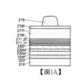
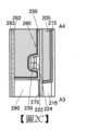
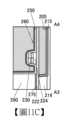
在本節中,說明形成圖1F所示的包括氧化物230(氧化物230a及氧化物230b)和氧化物230上的導電體242的疊層體的方法。也就是說,作為構成疊層體的氧化物半導體層設置氧化物230且作為導電體層設置導電體242。在圖1F所示的疊層體中,用作基底絕緣膜的絕緣體216及絕緣體222上設置有島狀的絕緣體224、島狀的氧化物230(氧化物230a及氧化物230b)、島狀的導電體242及島狀的絕緣體271(絕緣體271_1、絕緣體271_2)。In this section, a method of forming the laminate including the oxide 230 (the
氧化物230是用作氧化物半導體的金屬氧化物,例如可以被用作電晶體的活性層。在此情況下,接觸於氧化物230的頂面的導電體242可以被用作該電晶體的源極電極或汲極電極。The
以下,使用圖1A至圖1F說明包括絕緣體224、氧化物230、導電體242及絕緣體271的疊層體的加工的具體例子。Hereinafter, a specific example of processing the laminate including the
首先,在基板(未圖示)上依次沉積絕緣體216、絕緣體222、絕緣膜224f、氧化膜230af、氧化膜230bf、導電膜242f、絕緣膜271_1f及絕緣膜271_2f(參照圖1A)。在此,絕緣膜224f是將在後面的製程中成為絕緣體224的絕緣膜。另外,氧化膜230af是將在後面的製程中成為氧化物230a的金屬氧化物膜。另外,氧化膜230bf是將在後面的製程中成為氧化物230b的金屬氧化物膜。另外,導電膜242f是將在後面的製程中成為導電體242的導電膜。另外,絕緣膜271_1f是將在後面的製程中成為絕緣體271_1的絕緣膜。另外,絕緣膜271_2f是將在後面的製程中成為絕緣體271_2的絕緣膜。First, the
在此,絕緣膜271_1f及絕緣膜271_2f是將在後面的製程中被用作蝕刻停止膜的保護導電體242的膜。另外,絕緣膜271_1f接觸於導電膜242f,所以較佳為使用不容易使導電膜242f氧化的無機絕緣膜。絕緣膜271_1f較佳為使用氮化物絕緣體,例如較佳為使用氮化矽。另外,絕緣膜271_2f較佳為使用氧化物絕緣體,例如較佳為使用氧化矽。另外,也可以以不暴露於大氣的方式連續沉積絕緣膜271_1f及絕緣膜271_2f。Here, the insulating film 271_1f and the insulating film 271_2f are films that will be used as etching stop films to protect the
例如,絕緣體216及絕緣膜224f可以使用氧化矽。另外,例如,絕緣體222可以使用氧化鉿。另外,例如,氧化膜230af及氧化膜230bf可以使用包含In、Ga、Zn的氧化物。另外,例如,導電膜242f可以使用氮化鉭。另外,例如,導電膜242f也可以具有疊層結構,也可以具有包含氮化鉭的層與該包含氮化鉭的層上的包含鎢的層的疊層結構。For example, silicon oxide can be used for the
關於絕緣體216、絕緣體222、絕緣膜224f(絕緣體224)、氧化膜230af(氧化物230a)、氧化膜230bf(氧化物230b)、導電膜242f(導電體242)、絕緣膜271_1f(絕緣體271_1)及絕緣膜271_2f(絕緣體271_2)的詳細結構,將在<半導體裝置的結構例子>中進行說明。Regarding the
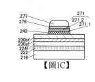
接著,在絕緣膜271_2f上沉積無機膜276f(參照圖1A)。無機膜276f的沉積可以藉由濺射法、CVD法、MBE法、PLD法或ALD法等進行。無機膜276f是將在後面的製程中用作用於形成氧化物230a、氧化物230b及絕緣體224的硬遮罩的膜。無機膜276f可以使用金屬材料或無機絕緣材料等。例如,作為無機膜276f可以使用藉由濺射法沉積的鎢。另外,也可以在沉積絕緣膜271_1f及絕緣膜271_2f之後以不暴露於大氣的方式連續沉積無機膜276f。Next, an inorganic film 276f is deposited on the insulating film 271_2f (see FIG. 1A). The inorganic film 276f can be deposited by sputtering, CVD, MBE, PLD or ALD. The inorganic film 276f is a film that will be used as a hard mask for forming the
接著,在無機膜276f上沉積塗佈膜277f,然後沉積塗佈膜278f(參照圖1A)。塗佈膜277f及塗佈膜278f也可以具有提高後述光阻遮罩與無機膜276的密接性的功能。塗佈膜277f及塗佈膜278f的沉積例如可以藉由旋塗法等進行。塗佈膜277f及塗佈膜278f可以使用非感光性有機樹脂。Next, the
在此,塗佈膜278f在加工塗佈膜277f的蝕刻處理中被用作遮罩。因此,在塗佈膜277f的蝕刻條件中,塗佈膜278f的蝕刻速率較佳為低於塗佈膜277f的蝕刻速率。例如,塗佈膜277f可以使用包含碳的膜且塗佈膜278f可以使用包含矽及碳的膜。在本實施方式中,作為塗佈膜277f沉積SOC(Spin On Carbon:旋塗碳)膜且作為塗佈膜278f沉積SOG(Spin On Glass:旋塗玻璃)膜。Here, the
另外,塗佈膜277f及塗佈膜278f在塗佈時包含醇等有機溶劑,但是在後續製程中或者在半導體裝置完成時,所含有的有機物有時減少或被去除。另外,塗佈膜根據需要設置即可,可以設置單層的塗佈膜,或者在僅使用後述光阻遮罩就足夠時也可以不設置塗佈膜。In addition, the
接著,利用光微影法在塗佈膜278f上形成光阻遮罩279(參照圖1A)。作為光阻遮罩279,使用也被稱為光阻劑的感光性有機樹脂即可。例如,可以使用正型光阻劑或負型光阻劑。例如,藉由使用旋塗法等沉積將成為光阻遮罩279的光阻劑,可以沉積為均勻的厚度。Next, a
注意,在光微影法中,首先藉由遮罩對光阻劑進行曝光。接著,使用顯影液去除或留下所曝光的區域而形成光阻遮罩。接著,隔著該光阻遮罩進行蝕刻處理來將導電體、半導體或絕緣體等加工為所希望的形狀。例如,可以使用KrF準分子雷射、ArF準分子雷射、EUV(Extreme Ultraviolet:極紫外)光等對光阻劑進行曝光來形成光阻遮罩。此外,也可以利用在基板和投影透鏡之間填滿液體(例如,水)的狀態下進行曝光的液浸技術。此外,也可以使用電子束或離子束代替上述光。此外,在使用電子束或離子束的情況下,有時可以不使用遮罩。Note that in photolithography, the photoresist is first exposed through a mask. Next, a developer is used to remove or leave the exposed areas to form a photoresist mask. Next, etching is performed through the photoresist mask to process the conductor, semiconductor, insulator, etc. into a desired shape. For example, KrF excimer laser, ArF excimer laser, EUV (Extreme Ultraviolet: extreme ultraviolet) light, etc. can be used to expose the photoresist to form a photoresist mask. Alternatively, a liquid immersion technology that performs exposure with a liquid (for example, water) filling the space between the substrate and the projection lens may be used. In addition, electron beams or ion beams may be used instead of the above-mentioned light. Additionally, in the case of using electron beams or ion beams, it is sometimes possible to eliminate the need for a mask.
以下,在根據圖1B至圖1F的製程中,藉由乾蝕刻法進行圖1A所示的疊層膜的蝕刻處理。乾蝕刻法可以進行各向異性蝕刻,因此適用於形成具有高縱橫比的包括絕緣體224、氧化物230、導電體242及絕緣體271的微型結構的疊層體。Next, in the process according to FIGS. 1B to 1F , the laminated film shown in FIG. 1A is etched by a dry etching method. The dry etching method can perform anisotropic etching, so it is suitable for forming a multilayer body with a high aspect ratio and a microstructure including the
在此,作為用於乾蝕刻處理的蝕刻氣體,可以使用包含鹵素的蝕刻氣體,明確而言,可以使用包含氟、氯和溴中的一個或多個的蝕刻氣體。作為蝕刻氣體,例如可以使用C4F6氣體、C5F6氣體、C4F8氣體、CF4氣體、SF6氣體、CHF3氣體、CH2F2氣體、Cl2氣體、BCl3氣體、SiCl4和BBr3氣體等中的一種或兩種以上的混合氣體。另外,可以對上述蝕刻氣體適當地添加氧氣體、碳酸氣體、氮氣體、氦氣體、氬氣體、氫氣體或烴氣體等。另外,根據乾蝕刻處理的被處理物,也可以使用不包含鹵素氣體而包含烴氣體或氫氣體的氣體作為蝕刻氣體。作為用於蝕刻氣體的烴,可以使用甲烷(CH4)、乙烷(C2H6)、丙烷(C3H8)、丁烷(C4H10)、乙烯(C2H4)、丙烯(C3H6)、乙炔(C2H2)及丙炔(C3H4)中的一個或多個。可以根據蝕刻對象適當地設定蝕刻條件。Here, as the etching gas used for the dry etching process, an etching gas containing halogen can be used. Specifically, an etching gas containing one or more of fluorine, chlorine, and bromine can be used. As the etching gas, for example, C4 F6 gas, C5 F6 gas, C4 F8 gas, CF4 gas, SF6 gas, CHF3 gas, CH2 F2 gas, Cl2 gas, and BCl3 gas can be used. , SiCl4 and BBr3 gas, etc. One or a mixture of two or more gases. In addition, oxygen gas, carbonic acid gas, nitrogen gas, helium gas, argon gas, hydrogen gas, hydrocarbon gas, etc. may be appropriately added to the etching gas. In addition, depending on the object to be processed in the dry etching process, a gas that does not contain halogen gas but contains hydrocarbon gas or hydrogen gas may be used as the etching gas. As the hydrocarbon used for the etching gas, methane (CH4 ), ethane (C2 H6 ), propane (C3 H8 ), butane (C4 H10 ), ethylene (C2 H4 ), One or more of propylene (C3 H6 ), acetylene (C2 H2 ) and propyne (C3 H4 ). Etching conditions can be appropriately set according to the etching target.
作為乾蝕刻裝置,例如可以使用包括平行平板型電極的電容耦合電漿(CCP:Capacitively Coupled Plasma)蝕刻裝置。包括平行平板型電極的電容耦合電漿蝕刻裝置也可以採用對平行平板型電極中的一個施加高頻電壓的結構。或者,也可以採用對平行平板型電極中的一個施加不同的多個高頻電壓的結構。或者,也可以採用對平行平板型電極的各個施加頻率相同的高頻電壓的結構。或者,也可以採用對平行平板型電極的各個施加頻率不同的高頻電壓的結構。或者,也可以利用具有高密度電漿源的乾蝕刻裝置。例如,作為具有高密度電漿源的乾蝕刻裝置,可以使用電感耦合電漿(ICP:Inductively Coupled Plasma)蝕刻裝置等。可以根據蝕刻對象適當地設定蝕刻裝置。As a dry etching apparatus, for example, a capacitively coupled plasma (CCP) etching apparatus including parallel plate electrodes can be used. The capacitively coupled plasma etching apparatus including parallel plate-type electrodes may have a structure in which a high-frequency voltage is applied to one of the parallel plate-type electrodes. Alternatively, a structure may be adopted in which a plurality of different high-frequency voltages are applied to one of the parallel plate electrodes. Alternatively, a structure may be adopted in which a high-frequency voltage with the same frequency is applied to each of the parallel plate-type electrodes. Alternatively, a structure may be adopted in which high-frequency voltages with different frequencies are applied to each of the parallel plate-shaped electrodes. Alternatively, a dry etching apparatus with a high-density plasma source may be used. For example, as a dry etching apparatus having a high-density plasma source, an inductively coupled plasma (ICP: Inductively Coupled Plasma) etching apparatus or the like can be used. The etching device can be appropriately set according to the etching target.
根據圖1B至圖1F的製程較佳為以不暴露於外部空氣的方式連續進行。例如,可以使用多室方式的蝕刻裝置以不暴露於外部空氣的方式進行處理。在此,較佳為使用CCP蝕刻裝置,該CCP蝕刻裝置在根據圖1B至圖1F的製程中對處理室內的平行平板型電極分別施加頻率不同的高頻電壓。在此情況下,可以對上部電極施加頻率高的高頻電壓而對設置基板的下部電極施加頻率低的高頻電壓。The process according to FIGS. 1B to 1F is preferably performed continuously without being exposed to external air. For example, a multi-chamber etching apparatus can be used to perform processing without being exposed to outside air. Here, it is preferable to use a CCP etching device, which applies high-frequency voltages with different frequencies to the parallel plate-type electrodes in the processing chamber during the process according to FIGS. 1B to 1F . In this case, a high-frequency high-frequency voltage may be applied to the upper electrode and a low-frequency high-frequency voltage may be applied to the lower electrode on which the substrate is provided.
首先,使用光阻遮罩279加工塗佈膜278f形成島狀的塗佈膜278。例如,在作為塗佈膜278f使用SOG膜時,可以使用CHF3及O2作為蝕刻氣體。First, the
接著,使用塗佈膜278作為遮罩加工塗佈膜277f形成島狀的塗佈膜277(參照圖1B)。例如,在作為塗佈膜277f使用SOC膜時,可以使用H2及N2作為蝕刻氣體。在此,作為塗佈膜278使用SOG膜,由此可以防止塗佈膜277f的蝕刻製程中塗佈膜278消失。Next, the
另外,較佳的是,在加工塗佈膜277f的同時去除光阻遮罩279。由於作為塗佈膜277f使用SOC膜,所以可以容易地去除光阻遮罩279。另外,在形成塗佈膜277之後殘留有光阻遮罩279時,較佳為去除光阻遮罩279。In addition, it is preferable to remove the
接著,使用塗佈膜277作為遮罩依次加工無機膜276f、絕緣膜271_2f、絕緣膜271_1f及導電膜242f而形成島狀的無機膜276、島狀的絕緣體271_1、島狀的絕緣體271_2及島狀的導電體242(參照圖1C)。例如,在作為無機膜276f使用鎢膜時,可以使用CF4及Cl2作為蝕刻氣體。另外,例如,在作為絕緣膜271_1f使用氮化矽且作為絕緣膜271_2f使用氧化矽時,在絕緣膜271_1f及絕緣膜271_2f的蝕刻中可以使用CHF3及O2作為蝕刻氣體。另外,例如,在作為導電膜242f使用氮化鉭膜時,可以使用CHF3、Cl2及Ar作為蝕刻氣體。另外,同樣地,在作為導電膜242f使用氮化鉭層與鎢層的疊層膜時也可以使用HF3、Cl2及Ar作為蝕刻氣體。Next, the inorganic film 276f, the insulating film 271_2f, the insulating film 271_1f and the
在此,有時作為無機膜276及導電膜242f使用相同金屬材料(例如,鎢等)。在用作遮罩的塗佈膜277在導電膜242f的蝕刻中消失時,無機膜276暴露於該蝕刻。由此,導電膜242f等被過度蝕刻而可能導致導電體242的寬度比設計時窄。Here, the same metal material (eg, tungsten, etc.) may be used as the
於是,在導電膜242f的蝕刻製程中,較佳為以導電膜242f的蝕刻速率高於塗佈膜277的蝕刻速率的條件進行蝕刻。例如,在導電膜242f的蝕刻製程中,較佳為降低設置有基板的下部電極的功耗。例如,設置有基板的下部電極的功耗可以低於上述蝕刻無機膜276f時的下部電極的功耗,較佳為低於25W,更佳為10W以下。藉由以上述條件進行蝕刻,即便在微型結構的疊層體中也可以按照設計進行加工。Therefore, in the etching process of the
另外,較佳為在加工絕緣膜271_1f及絕緣膜271_2f的同時去除塗佈膜278。由於作為絕緣膜271_1f及絕緣膜271_2f使用矽類絕緣膜,所以可以容易地去除塗佈膜278。In addition, it is preferable to remove the
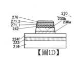
接著,使用無機膜276作為遮罩加工氧化膜230bf及氧化膜230af形成島狀的氧化物230b及島狀的氧化物230a(參照圖1D)。例如,在作為氧化膜230bf及氧化膜230af使用包含選自In、Ga和Zn中的任一個或多個的氧化物時,可以使用CH4及Ar作為蝕刻氣體。包含In、Ga、Zn的氧化物與CH3自由基起反應而易於形成揮發性高的金屬錯合物。因此,藉由使用包含CH4的氣體,即使基板溫度較低也可以容易地對作為難蝕刻材料的包含In、Ga、Zn的氧化物進行加工。Next, the oxide film 230bf and the oxide film 230af are processed using the
再者,在無機膜276包含鎢且絕緣膜224f包含矽氧化物的情況下,較佳為使用甲烷(CH4)氣體進行氧化膜230bf及氧化膜230af的蝕刻。藉由如此進行蝕刻,可以使氧化膜230bf及氧化膜230af的蝕刻速率顯著大於無機膜276及絕緣膜224f。因此,在本製程中,可以在絕緣膜224f平坦的狀態下將氧化膜230bf及氧化膜230af形成為島狀。由此,在後述將絕緣膜224f形成為島狀的製程中,可以徹底去除絕緣膜224f的不與氧化物230a重疊的區域,且可以防止絕緣體222被過蝕刻。Furthermore, when the
另外,較佳為在加工氧化膜230bf及氧化膜230af的同時去除塗佈膜277。注意,當在圖1D所示的製程之後塗佈膜277殘留時,藉由進行灰化等乾蝕刻處理、進行濕蝕刻處理、在進行乾蝕刻處理之後進行濕蝕刻處理或者在進行濕蝕刻處理之後進行乾蝕刻處理,去除塗佈膜277即可。In addition, it is preferable to remove the
另外,也可以在導電體242的形成結束後且加工氧化膜230bf及氧化膜230af之前去除塗佈膜277。In addition, the
接著,使用無機膜276加工絕緣膜224f形成島狀的絕緣體224(參照圖1E)。例如,在作為絕緣膜224f使用氧化矽膜時,可以使用CHF3及Ar作為蝕刻氣體。Next, the insulating
在此,在絕緣膜224f的加工中,絕緣體222較佳為不被過蝕刻。因此,較佳為在相對於絕緣體222的蝕刻選擇比大的條件下進行蝕刻。例如,在絕緣膜224f含矽氧化物且使用包含氟的氣體進行蝕刻的情況下,絕緣體222較佳為包含鉿氧化物。Here, it is preferable that the
最後,去除無機膜276(參照圖1F)。在此,絕緣體271_1及絕緣體271_2被用作蝕刻停止膜保護導電體242。在此,作為絕緣體271_2使用矽類氧化物絕緣膜,由此可以防止在有機膜276的蝕刻製程中絕緣體271_1及絕緣體271_2消失。Finally, the
例如,在作為無機膜276使用鎢膜時,可以使用CF4、Cl2及O2作為蝕刻氣體。另外,在無機膜276的材料沒有影響到後製程或者可以在後製程中使用時,並不需要必須去除無機膜276。For example, when a tungsten film is used as the
另外,在去除無機膜276的製程中,絕緣體271_1及絕緣體271_2被用作保護導電體242的遮罩,所以導電體242在側面與頂面間不具有彎曲面。因此,導電體242的側面與頂面交叉的端部成為角狀。在導電體242的側面與頂面交叉的端部成為角狀時,與該端部具有曲面的情況相比,導電體242的剖面積增大。再者,藉由作為絕緣體271_1使用不容易使金屬氧化的氮化物絕緣體,可以防止導電體242被過度氧化。由此,在將上述疊層體用於電晶體時,後面成為源極電極及汲極電極的導電體242的電阻得到降低,從而可以提高電晶體的通態電流。In addition, during the process of removing the
藉由上述製程,可以形成圖1F所示的島狀層疊體,其中導電體242的側面不相對於氧化物230的側面過度後退,換言之,導電體242的側端部與氧化物230的側端部大致對齊。藉由使用這種具有微型結構的疊層體製造電晶體,可以實現半導體裝置的微型化及高積體化。Through the above process, the island-shaped laminate shown in FIG. 1F can be formed, in which the side surfaces of the
另外,可以將絕緣體224、氧化物230a、氧化物230b、導電體242、絕緣體271_1及絕緣體271_2一次性地加工為島狀。由此,與將絕緣體224、氧化物230a、氧化物230b、導電體242、絕緣體271_1及絕緣體271_2分別加工為島狀地情況相比,可以減少製程數。由此,可以實現半導體裝置的生產率的提高。In addition, the
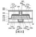
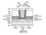
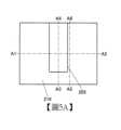
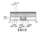
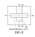
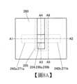
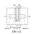
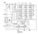
<半導體裝置的結構例子> 使用圖2至圖4說明使用上述疊層體的半導體裝置的結構例子。圖2A至圖2D是半導體裝置(電晶體200)的平面圖及剖面圖。圖2A是該半導體裝置的平面圖。另外,圖2B至圖2D是該半導體裝置的剖面圖。在此,圖2B是沿著圖2A中的點劃線A1-A2的部分的剖面圖,也是電晶體200的通道長度方向的剖面圖。此外,圖2C是沿著圖2A中的點劃線A3-A4的部分的剖面圖,也是電晶體200的通道寬度方向的剖面圖。另外,圖2D是沿著圖2A中的點劃線A5-A6的部分的剖面圖,也是電晶體200的通道寬度方向的剖面圖。注意,在圖2A的平面圖中,為了明確起見,省略一部分組件。另外,圖3A及圖3B示出電晶體200的通道長度方向的剖面放大圖,圖4A及圖4B示出電晶體200的通道寬度方向的剖面放大圖。<Structure example of semiconductor device> A structural example of a semiconductor device using the above-mentioned multilayer body will be described using FIGS. 2 to 4 . 2A to 2D are plan views and cross-sectional views of the semiconductor device (transistor 200). FIG. 2A is a plan view of the semiconductor device. In addition, FIGS. 2B to 2D are cross-sectional views of the semiconductor device. Here, FIG. 2B is a cross-sectional view along the dotted line A1 - A2 in FIG. 2A , and is also a cross-sectional view in the channel length direction of the
電晶體200包括:絕緣體215上的絕緣體216;以嵌入絕緣體216的方式設置的導電體205(導電體205a及導電體205b);絕緣體216及導電體205上的絕緣體222;絕緣體222上的絕緣體224;絕緣體224上的氧化物230(氧化物230a及氧化物230b);氧化物230上的導電體242a及導電體242b;導電體242a上的絕緣體271a(絕緣體271a1及絕緣體271a2);導電體242b上的絕緣體271b(絕緣體271b1及絕緣體271b2);氧化物230上的絕緣體250;以及絕緣體250上的導電體260(導電體260a及導電體260b)。The
絕緣體271a、271b上設置有絕緣體275,絕緣體275上設置有絕緣體280。絕緣體250及導電體260嵌入設置在絕緣體280及絕緣體275中的開口的內部。絕緣體280上及導電體260上設置有絕緣體282。另外,絕緣體282上設置有絕緣體283。The
氧化物230具有用作電晶體200的通道形成區域的區域。另外,導電體260具有用作電晶體200的第一閘極電極(上側的閘極電極)的區域。絕緣體250具有用作電晶體200的第一閘極絕緣體的區域。另外,導電體205具有用作電晶體200的第二閘極電極(下側的閘極電極)的區域。絕緣體224及絕緣體222都具有用作電晶體200的第二閘極絕緣體的區域。The
導電體242a具有用作電晶體200的源極電極和汲極電極中的一個的區域。導電體242b具有用作電晶體200的源極電極和汲極電極中的另一個的區域。The
如圖2B至圖2D所示,在從電晶體200的剖面看時,較佳的是,導電體242a的一個側端部與氧化物230的一個側端部大致對齊,並且導電體242b的一個側端部與氧化物230的另一個側端部大致對齊。再者,絕緣體224的側端部較佳為與氧化物230的側端部大致對齊。如上所述,本發明的一個實施方式可以將絕緣體224、氧化物230以及將成為導電體242a及導電體242b的導電體242一次性地加工為島狀。由此,可以以良好的生產率製造根據本發明的一個實施方式的半導體裝置。在上述那樣地加工時,絕緣體224、氧化物230、導電體242a及導電體242b的側端部如上所述地都大致對齊。As shown in FIGS. 2B to 2D , when viewed from the cross-section of the
另外,絕緣體271a及絕緣體271b在上述島狀的加工中被用作保護導電體242a及導電體242b的蝕刻停止層。因此,如圖2B及圖2D所示,在從電晶體200的剖面看時,較佳的是,絕緣體271a的側端部與導電體242a的側端部大致對齊,並且絕緣體271b的側端部與導電體242b的側端部大致對齊。In addition, the
在從剖面看時側端部對齊或大致對齊的情況下以及在頂面形狀一致或大致一致的情況下,可以說在俯視時至少其輪廓的一部分在層疊的各層間彼此重疊。例如,包括上層的側端部的下部接觸於下層的側端部的上部的情況。另外,例如,包括上層及下層藉由同一或其一部分同一遮罩圖案被加工的情況。但是,實際上有輪廓不重疊的情況,有時上層位於下層的內側或者上層位於下層的外側,這種情況也可以說“側端部大致對齊”或“頂面形狀大致一致”。When the side ends are aligned or substantially aligned when viewed in cross section and when the top surface shapes are consistent or substantially consistent, it can be said that at least part of the outlines overlap each other in plan view between the stacked layers. For example, this includes a case where the lower portion of the side end portion of the upper layer is in contact with the upper portion of the side end portion of the lower layer. In addition, for example, it includes the case where the upper layer and the lower layer are processed using the same or a part of the same mask pattern. However, there are cases where the contours do not actually overlap, and the upper layer may be located inside the lower layer or the upper layer may be located outside the lower layer. In this case, it can also be said that "the side ends are approximately aligned" or "the top surface shape is approximately the same."
氧化物230較佳為包括絕緣體224上的氧化物230a以及氧化物230a上的氧化物230b。藉由在氧化物230b之下設置氧化物230a,可以抑制雜質從形成在氧化物230a下方的結構物擴散到氧化物230b。
注意,本實施方式示出氧化物230具有氧化物230a及氧化物230b的兩層結構的例子,但是不侷限於此。氧化物230例如可以具有氧化物230b的單層結構,也可以具有三層以上的疊層結構。Note that this embodiment shows an example in which the
如圖3A所示,氧化物230b在電晶體200中具有區域230bc以及以夾著區域230bc的方式設置的區域230ba及區域230bb。在此,區域230bc被用作通道形成區域。另外,區域230ba被用作源極區域和汲極區域中的一方,區域230bb被用作源極區域和汲極區域中的另一方。區域230bc的至少一部分與導電體260重疊。區域230ba與導電體242a重疊,區域230bb與導電體242b重疊。As shown in FIG. 3A , the
由於與區域230ba及區域230bb相比其氧空位少或雜質濃度低,所以區域230bc是載子濃度低的高電阻區域。因此,區域230bc可以說是i型(本質)或實質上i型的區域。Since the region 230bc has fewer oxygen vacancies or a lower impurity concentration than the region 230ba and the region 230bb, the region 230bc is a high-resistance region with a low carrier concentration. Therefore, the region 230bc can be said to be an i-type (essentially) or substantially i-type region.
此外,區域230ba及區域230bb的氧空位多或者氫、氮、金屬元素等雜質濃度高,因此是載子濃度高的低電阻區域。就是說,區域230ba及區域230bb是比區域230bc載子濃度高的n型的區域(低電阻區域)。In addition, the regions 230ba and 230bb are low-resistance regions with a high carrier concentration because they have many oxygen vacancies or have a high concentration of impurities such as hydrogen, nitrogen, and metal elements. That is, the regions 230ba and the regions 230bb are n-type regions (low resistance regions) with a higher carrier concentration than the region 230bc.
區域230bc的載子濃度較佳為1×1018cm-3以下、低於1×1017cm-3、低於1×1016cm-3、低於1×1015cm-3、低於1×1014cm-3、低於1×1013cm-3、低於1×1012cm-3、低於1×1011cm-3或者低於1×1010cm-3。注意,對區域230bc的載子濃度的下限值沒有特別的限制,例如可以為1×10⁻⁹cm-3。The carrier concentration of the region 230bc is preferably less than 1×1018 cm-3 , less than 1×1017 cm-3 , less than 1×1016 cm-3 , less than 1×1015 cm-3 , less than 1×1014 cm-3 , lower than 1×1013 cm-3 , lower than 1×1012 cm-3 , lower than 1×1011 cm-3 or lower than 1×1010 cm-3 . Note that the lower limit value of the carrier concentration in the region 230bc is not particularly limited, and may be 1×10⁻⁹ cm-3 , for example.
在以降低氧化物230b的載子濃度為目的的情況下,可以降低氧化物230b中的雜質濃度以降低缺陷態密度。在本說明書等中,將雜質濃度低且缺陷態密度低的狀態稱為高純度本質或實質上高純度本質。此外,有時將載子濃度低的氧化物半導體(或金屬氧化物)稱為高純度本質或實質上高純度本質的氧化物半導體(或金屬氧化物)。When the purpose is to reduce the carrier concentration of the
因此,為了使電晶體200的電特性穩定,降低氧化物230b中的雜質濃度是有效的。為了降低氧化物230b中的雜質濃度,較佳為還降低附近膜中的雜質濃度。作為雜質有氫、氮、鹼金屬、鹼土金屬、鐵、鎳、矽等。注意,氧化物230b中的雜質例如是指構成氧化物230b的主要成分之外的元素。例如,濃度小於0.1原子%的元素可以說是雜質。Therefore, in order to stabilize the electrical characteristics of the
另外,區域230bc、區域230ba及區域230bb不僅可以形成在氧化物230b中還可以形成至氧化物230a中。In addition, the regions 230bc, 230ba, and 230bb may be formed not only in the
在氧化物230中,有時難以明確地觀察各區域的邊界。在各區域中檢測出的金屬元素和氫及氮等雜質元素的濃度並不需要按每區域分階段地變化,也可以在各區域中連續地變化。就是說,越接近區域230bc,金屬元素和氫及氮等雜質元素的濃度也可以越低。In the
此外,較佳為將用作半導體的金屬氧化物(以下也稱為氧化物半導體)用於氧化物230(氧化物230a及氧化物230b)。In addition, it is preferable to use a metal oxide used as a semiconductor (hereinafter also referred to as an oxide semiconductor) for the oxide 230 (the
被用作半導體的金屬氧化物的能帶間隙較佳為2eV以上,更佳為2.5eV以上。藉由使用能帶間隙較寬的金屬氧化物,可以減小電晶體的關態電流(off-state current)。因此,將在通道形成區域中包含金屬氧化物的電晶體稱為OS電晶體。OS電晶體的關態電流小,所以可以充分降低半導體裝置的功耗。另外,OS電晶體的頻率特性高,所以可以使半導體裝置高速工作。The energy band gap of the metal oxide used as a semiconductor is preferably 2 eV or more, more preferably 2.5 eV or more. By using metal oxides with wider energy band gaps, the off-state current of the transistor can be reduced. Therefore, a transistor containing a metal oxide in a channel formation region is called an OS transistor. The off-state current of the OS transistor is small, so the power consumption of the semiconductor device can be significantly reduced. In addition, the OS transistor has high frequency characteristics, so the semiconductor device can be operated at high speed.
氧化物230較佳為包含金屬氧化物(氧化物半導體)。作為能夠用於氧化物230的金屬氧化物,例如,可以舉出銦氧化物、鎵氧化物及鋅氧化物。金屬氧化物較佳為至少包含銦(In)或鋅(Zn)。金屬氧化物較佳為包含選自銦、元素M和鋅中的兩個或三個。另外,元素M是與氧的鍵能高的金屬元素或準金屬元素,例如為與氧的鍵能高於銦的金屬元素或準金屬元素。明確而言,作為元素M,可以舉出鋁、鎵、錫、釔、鈦、釩、鉻、錳、鐵、鈷、鎳、鋯、鉬、鉿、鉭、鎢、鑭、鈰、釹、鎂、鈣、鍶、鋇、硼、矽、鍺及銻等。金屬氧化物所包含的元素M較佳為上述元素中的任一種或多種,更佳為選自鋁、鎵、錫和釔中的一種或多種,進一步較佳為鎵。另外,在本說明書等中,有時將金屬元素及準金屬元素統稱為“金屬元素”,並且本說明書等所記載的“金屬元素”有時包括準金屬元素。
氧化物230例如可以使用銦鋅氧化物(In-Zn氧化物)、銦錫氧化物(In-Sn氧化物)、銦鈦氧化物(In-Ti氧化物)、銦鎵氧化物(In-Ga氧化物)、銦鎵鋁氧化物(In-Ga-Al氧化物)、銦鎵錫氧化物(In-Ga-Sn氧化物)、鎵鋅氧化物(Ga-Zn氧化物,也記作GZO)、鋁鋅氧化物、銦鋁鋅氧化物(In-Al-Zn氧化物,也記作IAZO)、銦錫鋅氧化物(In-Sn-Zn氧化物)、銦鈦鋅氧化物(In-Ti-Zn氧化物)、銦鎵鋅氧化物(In-Ga-Zn氧化物,也記作IGZO)、銦鎵錫鋅氧化物(In-Ga-Sn-Zn氧化物,也記作IGZTO)、銦鎵鋁鋅氧化物(In-Ga-Al-Zn氧化物,也記作IGAZO或IAGZO)等。或者,可以使用包含矽的銦錫氧化物、鎵錫氧化物(Ga-Sn氧化物)、鋁錫氧化物(Al-Sn氧化物)等。As the
此時,藉由提高包含在金屬氧化物中的相對於所有金屬元素的原子個數的總和的銦的原子個數比,可以提高電晶體的場效移動率。In this case, by increasing the atomic number ratio of indium contained in the metal oxide relative to the total number of atoms of all metal elements, the field effect mobility of the transistor can be increased.
另外,金屬氧化物也可以代替銦或者除了銦以外還包含一種或多種週期數大的金屬元素。金屬元素的軌域重疊越大,金屬氧化物中的載子傳導趨於越大。因此,藉由包含週期數大的金屬元素,有時可以提高電晶體的場效移動率。作為週期數大的金屬元素,可以舉出屬於第5週期的金屬元素及屬於第6週期的金屬元素等。作為該金屬元素,明確而言,可以舉出:釔、鋯、銀、鎘、錫、銻、鋇、鉛、鉍、鑭、鈰、鐠、釹、鉕、釤及銪等。另外,鑭、鈰、鐠、釹、鉕、釤及銪被稱為輕稀土元素。In addition, the metal oxide may replace indium or contain one or more metal elements with a large period number in addition to indium. The greater the orbital overlap of a metallic element, the greater the carrier conduction in the metal oxide tends to be. Therefore, by including a metal element with a large period number, the field effect mobility of the transistor can sometimes be increased. Examples of metal elements with a large period number include metal elements belonging to the fifth period, metal elements belonging to the sixth period, and the like. Specific examples of the metal element include yttrium, zirconium, silver, cadmium, tin, antimony, barium, lead, bismuth, lanthanum, cerium, chelium, neodymium, cadmium, samarium, europium, and the like. In addition, lanthanum, cerium, cerium, neodymium, cadmium, samarium and europium are called light rare earth elements.
另外,金屬氧化物也可以包含一種或多種非金屬元素。在金屬氧化物包含非金屬元素時,有時可以提高電晶體的場效移動率。作為非金屬元素,例如可以舉出碳、氮、磷、硫、硒、氟、氯、溴及氫等。In addition, metal oxides may also contain one or more non-metal elements. When the metal oxide contains non-metal elements, the field effect mobility of the transistor can sometimes be increased. Examples of non-metal elements include carbon, nitrogen, phosphorus, sulfur, selenium, fluorine, chlorine, bromine and hydrogen.
另外,藉由提高包含在金屬氧化物中的相對於所有金屬元素的原子個數的總和的鋅的原子個數比,金屬氧化物的結晶性提高,由此可以抑制金屬氧化物中的雜質的擴散。因此,電晶體的電特性變動被抑制,由此可以提高可靠性。In addition, by increasing the atomic number ratio of zinc contained in the metal oxide to the total number of atoms of all metal elements, the crystallinity of the metal oxide is improved, thereby suppressing the formation of impurities in the metal oxide. spread. Therefore, variations in the electrical characteristics of the transistor are suppressed, thereby improving reliability.
另外,藉由提高包含在金屬氧化物中的相對於所有金屬元素的原子個數的總和的元素M的原子個數比,可以抑制金屬氧化物中形成氧空位。因此,起因於氧空位的載子的生成被抑制,由此可以實現關態電流小的電晶體。另外,電晶體的電特性變動被抑制,由此可以提高可靠性。In addition, by increasing the atomic number ratio of element M contained in the metal oxide relative to the total number of atoms of all metal elements, the formation of oxygen vacancies in the metal oxide can be suppressed. Therefore, the generation of carriers due to oxygen vacancies is suppressed, so that a transistor with a small off-state current can be realized. In addition, fluctuations in the electrical characteristics of the transistor are suppressed, thereby improving reliability.
如上所述,根據用於氧化物230的金屬氧化物的組成而電晶體的電特性及可靠性不同。因此,藉由對應於電晶體所需的電特性及可靠性使金屬氧化物的組成不同,可以實現兼具優異的電特性及高可靠性的半導體裝置。As described above, the electrical characteristics and reliability of the transistor differ depending on the composition of the metal oxide used for the
氧化物230較佳為具有化學組成互不相同的多個氧化物層的疊層結構。例如,用於氧化物230a的金屬氧化物中的相對於主要成分的金屬元素的元素M的原子個數比較佳為大於用於氧化物230b的金屬氧化物中的相對於主要成分的金屬元素的元素M的原子個數比。此外,用於氧化物230a的金屬氧化物中的相對於In的元素M的原子個數比較佳為大於用於氧化物230b的金屬氧化物中的相對於In的元素M的原子個數比。藉由採用該結構,可以抑制雜質及氧從形成在氧化物230a的下方的結構物向氧化物230b擴散。The
此外,較佳的是,用於氧化物230b的金屬氧化物中的相對於元素M的In的原子個數比大於用於氧化物230a的金屬氧化物中的相對於元素M的In的的原子個數比。藉由採用該結構,電晶體200可以得到大通態電流及高頻率特性。In addition, it is preferable that the atomic number ratio of In relative to the element M in the metal oxide used for the
此外,氧化物230a及氧化物230b除了氧以外還包含共同元素作為主要成分,所以可以降低氧化物230a與氧化物230b的介面的缺陷態密度。由此介面散射給載子傳導帶來的影響變小,從而電晶體200可以得到大通態電流及高頻率特性。In addition, the
明確而言,作為氧化物230a可以使用In:M:Zn=1:3:2[原子個數比]或其附近的組成、In:M:Zn=1:3:4[原子個數比]或其附近的組成或者In:M:Zn=1:1:0.5[原子個數比]或其附近的組成的金屬氧化物。此外,作為氧化物230b,可以使用In:M:Zn=1:1:1[原子個數比]或其附近的組成、In:M:Zn=1:1:1.2[原子個數比]或其附近的組成、In:M:Zn=1:1:2[原子個數比]或其附近的組成、In:M:Zn=4:2:3[原子個數比]或其附近的組成的金屬氧化物。注意,附近的組成包括所希望的原子個數比的±30%的範圍。此外,作為元素M較佳為使用鎵。此外,作為氧化物230設置氧化物230b的單層的情況下,作為氧化物230b也可以適用可用於氧化物230a的金屬氧化物。此外,可用於氧化物230a及氧化物230b的金屬氧化物的組成不侷限於此。例如,可用於氧化物230a的金屬氧化物的組成也可以適用於氧化物230b。同樣地,可用於氧化物230b的金屬氧化物的組成也可以適用於氧化物230a。Specifically, as the
此外,在藉由濺射法沉積金屬氧化物時,上述原子個數比不侷限於所沉積的金屬氧化物的原子個數比,而也可以是用於金屬氧化物的沉積的濺射靶材的原子個數比。In addition, when depositing metal oxides by sputtering, the above-mentioned atomic number ratio is not limited to the atomic number ratio of the deposited metal oxide, but may also be a sputtering target used for the deposition of metal oxides. ratio of the number of atoms.
氧化物230b較佳為具有結晶性。尤其是,較佳為使用CAAC-OS(c-axis aligned crystalline oxide semiconductor:c軸配向結晶氧化物半導體)作為氧化物230b。
CAAC-OS具有結晶性高的緻密結構且是雜質及缺陷(例如,氧空位)少的金屬氧化物。尤其是,藉由在形成金屬氧化物後以金屬氧化物不被多晶化的溫度(例如,400℃以上且600℃以下)進行熱處理,可以使CAAC-OS具有結晶性更高的緻密結構。如此,藉由進一步提高CAAC-OS的密度,可以進一步降低該CAAC-OS中的雜質或氧的擴散。CAAC-OS has a dense structure with high crystallinity and is a metal oxide with few impurities and defects (for example, oxygen vacancies). In particular, by performing heat treatment after forming the metal oxide at a temperature at which the metal oxide is not polycrystallized (for example, 400° C. or more and 600° C. or less), CAAC-OS can be given a dense structure with higher crystallinity. In this way, by further increasing the density of CAAC-OS, the diffusion of impurities or oxygen in the CAAC-OS can be further reduced.
此外,在CAAC-OS中不容易觀察明確的晶界,因此不容易發生起因於晶界的電子移動率的下降。因此,包含CAAC-OS的金屬氧化物的物理性質穩定。因此,具有CAAC-OS的金屬氧化物具有耐熱性且可靠性高。In addition, in CAAC-OS, clear grain boundaries are not easily observed, so a decrease in electron mobility due to grain boundaries is less likely to occur. Therefore, the physical properties of metal oxides containing CAAC-OS are stable. Therefore, metal oxides with CAAC-OS are heat-resistant and highly reliable.
此外,藉由作為氧化物230b使用CAAC-OS等具有結晶性的氧化物,可以抑制源極電極或汲極電極從氧化物230b抽出氧。因此,即使進行熱處理也可以減少氧從氧化物230b被抽出,所以電晶體200對製程中的高溫度(所謂熱積存:thermal budget)也很穩定。In addition, by using a crystalline oxide such as CAAC-OS as the
在使用氧化物半導體的電晶體中,如果在氧化物半導體的形成通道的區域中存在雜質及氧空位,電特性則容易變動,有時降低可靠性。此外,氧空位附近的氫形成氫進入氧空位中的缺陷(下面有時稱為VOH)而可能會產生成為載子的電子。因此,當在氧化物半導體的形成通道的區域230bc中包含氧空位時,電晶體會具有常開啟特性(即使不對閘極電極施加電壓也存在通道而在電晶體中電流流過的特性)。由此,在氧化物半導體的區域230bc中,較佳為儘量減少雜質、氧空位及VOH。換言之,較佳的是,氧化物半導體中的區域230bc的載子濃度降低且被i型化(本質化)或實質上被i型化。In a transistor using an oxide semiconductor, if impurities and oxygen vacancies are present in a region of the oxide semiconductor where a channel is formed, the electrical characteristics are likely to vary, which may reduce reliability. In addition, the hydrogen near the oxygen vacancy may form a defect (hereinafter sometimes referred to as VO H) in which hydrogen enters the oxygen vacancy, thereby generating electrons that become carriers. Therefore, when oxygen vacancies are included in the channel-forming region 230bc of the oxide semiconductor, the transistor will have a normally-on characteristic (a characteristic in which a channel exists and current flows in the transistor even if no voltage is applied to the gate electrode). Therefore, in the oxide semiconductor region 230bc, it is preferable to reduce impurities, oxygen vacancies, and VO H as much as possible. In other words, it is preferable that the carrier concentration of the region 230bc in the oxide semiconductor is reduced and is made into an i-type (essentially made) or substantially made into an i-type.
相對於此,藉由在氧化物半導體附近設置包含藉由加熱脫離的氧(以下,有時稱為過量氧)的絕緣體而進行熱處理,可以從該絕緣體向氧化物半導體供應氧而減少氧空位及VOH。注意,在對區域230ba或區域230bb供應過多的氧時,有可能引起電晶體200的通態電流下降或者場效移動率的下降。並且,在供應到區域230ba或區域230bb的氧量在基板面內有不均勻時,包括電晶體的半導體裝置特性發生不均勻。此外,在從該絕緣體供應給氧化物半導體的氧擴散到閘極電極、源極電極及汲極電極等導電體時,有時該導電體被氧化,這導致導電性的損失,因此對電晶體的電特性及可靠性帶來負面影響。On the other hand, by providing an insulator containing oxygen desorbed by heating (hereinafter sometimes referred to as excess oxygen) near an oxide semiconductor and performing heat treatment, oxygen can be supplied from the insulator to the oxide semiconductor to reduce oxygen vacancies and VO H. Note that when too much oxygen is supplied to the region 230ba or the region 230bb, it may cause the on-state current of the
因此,較佳的是,在氧化物半導體中,區域230bc的載子濃度得到降低且被i型化或實質上被i型化,另一方面,較佳的是,區域230ba及區域230bb的載子濃度高且被n型化。換言之,較佳為減少氧化物半導體的區域230bc的氧空位及VOH。此外,較佳的是,區域230ba及區域230bb不被供應過多的氧以及不被降低過剩的區域230ba及區域230bb的VOH量。此外,較佳為具有抑制導電體260、導電體242a及導電體242b等的導電率的降低的結構。例如,較佳為具有抑制導電體260、導電體242a及導電體242b等的氧化的結構。注意,氧化物半導體中的氫可能會形成VOH,因此為了降低VOH量,需要降低氫濃度。Therefore, in the oxide semiconductor, it is preferable that the carrier concentration of the region 230bc is reduced and converted to i-type or substantially i-type. On the other hand, it is preferable that the carrier concentration of the region 230ba and the region 230bb is reduced. The subconcentration is high and it is n-type. In other words, it is preferable to reduce oxygen vacancies and VO H in the region 230bc of the oxide semiconductor. In addition, it is preferable that the region 230ba and the region 230bb are not supplied with excessive oxygen and that the excessive VO H amount of the region 230ba and the region 230bb is not reduced. In addition, it is preferable to have a structure that suppresses a decrease in the conductivity of the
於是,本實施方式中半導體裝置具有如下結構:降低區域230bc的氫濃度;抑制導電體242a、導電體242b及導電體260的氧化;以及抑制區域230ba及區域230bb中的氫濃度的降低。Therefore, the semiconductor device in this embodiment has a structure that reduces the hydrogen concentration in the region 230bc, suppresses oxidation of the
與氧化物230b中的區域230bc接觸的絕緣體250較佳為具有俘獲並固定氫的功能。由此,可以降低氧化物230b的區域230bc中的氫濃度。因此,可以降低區域230bc中的VOH而使區域230bci型化或實質上i型化。The
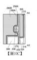
在此,如圖3A及圖4A所示,絕緣體250較佳為具有與氧化物230接觸的絕緣體250a、絕緣體250a上的絕緣體250b及絕緣體250b上的絕緣體250c的疊層結構。此時,絕緣體250a較佳為具有俘獲並固定氫的功能。Here, as shown in FIGS. 3A and 4A , the
作為具有俘獲並固定氫的功能的絕緣體,可以舉出具有非晶結構的金屬氧化物。作為絕緣體250a,例如,較佳為使用氧化鎂或者包含鋁和鉿中的一者或兩者的氧化物等金屬氧化物。上述具有非晶結構的金屬氧化物有時具有如下性質:氧原子具有懸空鍵而由該懸空鍵俘獲或固定氫。就是說,可以說具有非晶結構的金屬氧化物的俘獲或固定氫的能力高。Examples of the insulator having the function of capturing and fixing hydrogen include metal oxides having an amorphous structure. As the
另外,絕緣體250a較佳為使用高介電常數(high-k)材料。作為high-k材料的一個例子,有包含鋁和鉿中的一者或兩者的氧化物。當作為絕緣體250a使用high-k材料時,可以在保持閘極絕緣體的物理厚度的同時降低在電晶體工作時施加的閘極電位。此外,可以減少用作閘極絕緣體的絕緣體的等效氧化物厚度(EOT)。In addition, the
由此,作為絕緣體250a,較佳為使用包含鋁和鉿中的一者或兩者的氧化物,更佳為使用具有非晶結構並包含鋁和鉿中的一者或兩者的氧化物,進一步較佳為使用具有非晶結構的氧化鋁。在本實施方式中,作為絕緣體250a,使用氧化鋁。此時,絕緣體250a為至少包含氧及鋁的絕緣體。另外,該氧化鋁具有非晶結構。此時,絕緣體250a具有非晶結構。Therefore, as the
接著,作為絕緣體250b較佳為使用氧化矽或氧氮化矽等具有對熱穩定的結構的絕緣體。注意,在本說明書等中,“氧氮化物”是指在其組成中氧含量多於氮含量的材料,而“氮氧化物”是指在其組成中氮含量多於氧含量的材料。例如,在記載為“氧氮化矽”時指在其組成中氧含量多於氮含量的材料,而在記載為“氮氧化矽”時指在其組成中氮含量多於氧含量的材料。Next, it is preferable to use an insulator having a thermally stable structure such as silicon oxide or silicon oxynitride as the
另外,如圖3B及圖4B所示,也可以採用絕緣體250b上設置有絕緣體250d的結構。在此情況下,作為絕緣體250d可以設置可用作絕緣體250a的絕緣體。例如,作為絕緣體250d可以使用氧化鉿。在此,藉由在絕緣體250c與絕緣體250b間設置絕緣體250d,可以更有效地俘獲並固定含在絕緣體250b等中的氫。In addition, as shown in FIGS. 3B and 4B , an
再者,為了抑制導電體242a、導電體242b及導電體260的氧化,較佳為在導電體242a、導電體242b及導電體260的每一個附近設置氧阻擋絕緣體。在本實施方式所說明的半導體裝置中,該絕緣體例如為絕緣體250a、絕緣體250c、絕緣體250d及絕緣體275。Furthermore, in order to suppress oxidation of the
此外,在本說明書等中,阻擋絕緣體是指具有阻擋性的絕緣體。在本說明書等中,阻擋性是指抑制所對應的物質的擴散的功能(也可以說透過性低)。或者,是指俘獲並固定所對應的物質(也稱為吸雜)的功能。In addition, in this specification and the like, a barrier insulator means an insulator having barrier properties. In this specification and others, barrier properties refer to the function of suppressing the diffusion of the corresponding substance (it can also be said that the permeability is low). Or, it refers to the function of capturing and fixing the corresponding substance (also called gettering).
作為氧阻擋絕緣體,例如可以舉出包含鋁和鉿中的一者或兩者的氧化物、氧化鎂、氧化鎵、銦鎵鋅氧化物、氮化矽及氮氧化矽。另外,作為包含鋁和鉿中的一者或兩者的氧化物,例如可以舉出氧化鋁、氧化鉿、包含鋁及鉿的氧化物(鋁酸鉿)、包含鉿及矽的氧化物(矽酸鉿)。例如,絕緣體250a、絕緣體250c及絕緣體275較佳為採用上述氧阻擋絕緣體的單層或疊層。Examples of the oxygen barrier insulator include oxides containing one or both of aluminum and hafnium, magnesium oxide, gallium oxide, indium gallium zinc oxide, silicon nitride, and silicon oxynitride. Examples of oxides containing one or both of aluminum and hafnium include aluminum oxide, hafnium oxide, oxides containing aluminum and hafnium (hafnium aluminate), and oxides containing hafnium and silicon (silicon). Hafnium acid). For example, the
絕緣體250a較佳為具有氧阻擋性。絕緣體250a較佳為至少比絕緣體280不容易使氧透過。絕緣體250a具有與導電體242a的側面及導電體242b的側面接觸的區域。當絕緣體250a具有氧阻擋性時,可以抑制導電體242a及導電體242b的側面被氧化而在該側面上形成氧化膜。因此,可以抑制導致電晶體200的通態電流的下降或場效移動率的下降。The
絕緣體250a以與氧化物230b的頂面及側面、氧化物230a的側面、絕緣體224的側面及絕緣體222的頂面接觸的方式設置。當絕緣體250a具有氧阻擋性時,可以抑制在進行熱處理等時氧從氧化物230b的區域230bc脫離。因此,可以減少在氧化物230a及氧化物230b中形成氧空位。The
另外,藉由設置絕緣體250a,即使絕緣體280包含過多氧也可以抑制該氧過度供應到氧化物230a及氧化物230b而可以將適當量的氧供應到氧化物230a及氧化物230b。因此,可以抑制因區域230ba及區域230bb被過度氧化而導致電晶體200的通態電流的下降或場效移動率的下降。In addition, by providing the
因為包含鋁和鉿中的一者或兩者的氧化物具有氧阻擋性,所以可以適當地用作絕緣體250a。Since an oxide containing one or both of aluminum and hafnium has oxygen barrier properties, it can be suitably used as the
絕緣體250c較佳為具有氧阻擋性。絕緣體250c設置在氧化物230的區域230bc與導電體260之間以及絕緣體280與導電體260之間。藉由採用該結構,可以抑制氧化物230的區域230bc中的氧擴散到導電體260而在氧化物230的區域230bc中形成氧空位。另外,可以抑制氧化物230中的氧及絕緣體280中的氧擴散到導電體260而導致導電體260的氧化。絕緣體250c較佳為至少比絕緣體280不容易使氧透過。例如,作為絕緣體250c較佳為使用氮化矽。此時,絕緣體250c為至少包含氮及矽的絕緣體。The
此外,絕緣體250c較佳為具有氫阻擋性。由此,可以防止包含在導電體260中的氫等雜質擴散到氧化物230b。In addition, the
絕緣體275較佳為具有氧阻擋性。絕緣體275設置在絕緣體280與導電體242a之間以及絕緣體280與導電體242b之間。藉由採用該結構,可以抑制包含在絕緣體280中的氧擴散到導電體242a及導電體242b。因此,可以抑制包含在絕緣體280中的氧導致導電體242a及導電體242b被氧化使得電阻率增大而通態電流減少。絕緣體275較佳為至少比絕緣體280不容易使氧透過。例如,作為絕緣體275較佳為使用氮化矽。此時,絕緣體275為至少包含氮及矽的絕緣體。
為了抑制氧化物230中的區域230ba及區域230bb中的氫濃度降低,較佳為在區域230ba的附近及區域230bb的附近設置氫阻擋絕緣體。在本實施方式所說明的半導體裝置中,該氫阻擋絕緣體例如是絕緣體275。In order to suppress a decrease in the hydrogen concentration in the region 230ba and the region 230bb in the
作為氫阻擋絕緣體,可以舉出氧化鋁、氧化鉿、氧化鉭等氧化物、以及氮化矽等氮化物。例如,作為絕緣體275較佳為採用上述氫阻擋絕緣體的單層結構或疊層結構。Examples of the hydrogen barrier insulator include oxides such as aluminum oxide, hafnium oxide, and tantalum oxide, and nitrides such as silicon nitride. For example, the
絕緣體275較佳為具有氫阻擋性。當絕緣體275具有氫阻擋性時,可以防止絕緣體250俘獲並固定區域230ba及區域230bb中的氫。因此,區域230ba及區域230bb可以被n型化。
藉由採用上述結構,區域230bc可以被i型化或實質上被i型化且區域230ba及區域230bb可以被n型化,可以提供一種具有良好的電特性的半導體裝置。藉由採用上述結構,即便使半導體裝置微型化或高積體化也可以使其具有良好的電特性。此外,藉由使電晶體200微型化可以提高高頻特性。明確而言,可以提高截止頻率。By adopting the above structure, the region 230bc can be made into an i-type or substantially an i-type and the regions 230ba and 230bb can be made into an n-type, thereby providing a semiconductor device with good electrical characteristics. By adopting the above structure, the semiconductor device can have good electrical characteristics even if it is miniaturized or highly integrated. In addition, high-frequency characteristics can be improved by miniaturizing the
絕緣體250a至絕緣體250d被用作第一閘極絕緣體的一部分。絕緣體250a至絕緣體250d與導電體260一起設置在形成於絕緣體280等中的開口中。為了實現電晶體200的微型化,絕緣體250a至絕緣體250d的厚度較佳為薄。絕緣體250a至絕緣體250d的厚度分別較佳為0.1nm以上且10nm以下,更佳為0.1nm以上且5.0nm以下,進一步較佳為0.5nm以上且5.0nm以下,還進一步較佳為1.0nm以上且小於5.0nm,更進一步較佳為1.0nm以上且3.0nm以下。此外,絕緣體250a至絕緣體250d的至少一部分包括上述那樣的厚度的區域即可。
為了如上所述地減小絕緣體250a至絕緣體250d的厚度,較佳為利用原子層沉積(ALD:Atomic Layer Deposition)法進行沉積。ALD法有只利用熱能使前驅物及反應物起反應的熱ALD(Thermal ALD)法、使用收到電漿激發的反應物的PEALD(Plasma Enhanced ALD)法等。在PEALD法中,藉由利用電漿可以在更低溫下進行沉積,所以有時是較佳的。In order to reduce the thickness of the
ALD法可以按層沉積原子,從而有能夠沉積極薄的膜、能夠對縱橫比高的結構進行沉積、能夠以針孔等的缺陷少的方式進行沉積、能夠進行覆蓋性優良的沉積及能夠在低溫下進行沉積等效果。因此,可以在形成於絕緣體280等中的開口部的側面以及導電體242a、242b的側端部等以上述較小的厚度且高覆蓋性沉積絕緣體250。The ALD method can deposit atoms in layers, so it is possible to deposit extremely thin films, to deposit structures with a high aspect ratio, to deposit with few defects such as pinholes, to deposit with excellent coverage, and to be able to Deposition and other effects are performed at low temperatures. Therefore, the
ALD法中使用的前驅物有時包含碳等。因此,利用ALD法形成的膜有時與利用其它的沉積方法形成的膜相比包含更多的碳等雜質。此外,雜質的定量可以利用二次離子質譜分析法(SIMS:Secondary Ion Mass Spectrometry)、X射線光電子能譜(XPS:X-ray Photoelectron Spectroscopy)或俄歇電子能譜(AES:Auger Electron Spectroscopy)進行。The precursor used in the ALD method may contain carbon and the like. Therefore, a film formed by the ALD method may contain more impurities such as carbon than a film formed by other deposition methods. In addition, impurities can be quantified using secondary ion mass spectrometry (SIMS), X-ray photoelectron spectroscopy (XPS) or Auger Electron Spectroscopy (AES). .
注意,在上述中說明絕緣體250具有絕緣體250a至絕緣體250c的三層結構或絕緣體250a至絕緣體250d的四層結構,但本發明不侷限於此。絕緣體250可以具有包括絕緣體250a至絕緣體250d中的至少一個的結構。藉由絕緣體250由絕緣體250a至絕緣體250d中的一層、兩層或三層構成,可以簡化半導體裝置的製程,由此可以提高生產率。Note that it is described above that the
在本實施方式中,較佳的是,半導體裝置除了上述結構以外還具有抑制氫混入電晶體200等的結構。例如,較佳的是,以覆蓋電晶體200等的上方和下方中的一者或兩者的方式設置具有抑制氫擴散的功能的絕緣體。在本實施方式中說明的半導體裝置中,該絕緣體例如為絕緣體282及絕緣體283等。另外,電晶體200下的絕緣體215也可以具有與絕緣體282和絕緣體283中的任一者或兩者同樣的結構。在此情況下,絕緣體215可以具有絕緣體282與絕緣體283的疊層結構,可以採用絕緣體282位於下方且絕緣體283位於上方的結構,也可以採用絕緣體282位於上方且絕緣體283位於下方的結構。In this embodiment, it is preferable that the semiconductor device has a structure that suppresses the incorporation of hydrogen into the
絕緣體282和絕緣體283中的一個或多個較佳為被用作抑制水、氫等雜質從基板一側或電晶體200等的上方擴散到電晶體200等的阻擋絕緣體。因此,絕緣體282和絕緣體283中的一個或多個較佳為包含具有抑制氫原子、氫分子、水分子、氮原子、氮分子、氧化氮分子(N2O、NO、NO2等)、銅原子等雜質的擴散的功能(不容易使上述雜質透過)的絕緣材料。此外,較佳為包括具有抑制氧(例如,氧原子、氧分子等中的至少一個)的擴散的功能(不容易使上述氧透過)的絕緣材料。One or more of the
絕緣體282及絕緣體283較佳為分別包括具有抑制水、氫等雜質及氧的擴散的功能的絕緣體,例如可以使用氧化鋁、氧化鎂、氧化鉿、氧化鎵、銦鎵鋅氧化物、氮化矽或氮氧化矽等。例如,作為絕緣體283,較佳為使用氫阻擋性更高的氮化矽等。此外,例如,絕緣體282較佳為包括俘獲並固定氫的性能高的氧化鋁或氧化鎂等。由此,可以抑制水、氫等雜質從配置在絕緣體283的外側的層間絕緣膜等擴散到電晶體200等。或者,可以抑制含在絕緣體280等中的氧經過絕緣體282等向電晶體200等的上方擴散。另外,藉由作為絕緣體215採用與絕緣體282和絕緣體283中的一者或兩者同樣的結構,可以抑制水、氫等雜質從基板一側透過絕緣體215擴散到電晶體200等。另外,可以抑制含在絕緣體224等中的氧擴散到基板一側。像這樣,較佳為採用具有抑制水、氫等雜質及氧的擴散的功能的絕緣體圍繞電晶體200等的上方及下方的結構。The
在電晶體200中,導電體205以與氧化物230及導電體260重疊的方式配置。在此,導電體205較佳為以嵌入形成在絕緣體216中的開口部的方式設置。此外,如圖2A及圖2C所示,導電體205較佳為延伸設置在通道寬度方向上。藉由採用這種結構,在設置多個電晶體時導電體205被用作佈線。In the
導電體205可以具有單層結構或疊層結構。在圖2等中,導電體205包括導電體205a及導電體205b。導電體205a以與上述開口部的底面及側壁接觸的方式設置。導電體205b以嵌入沿著上述開口部形成的導電體205a的凹部中的方式設置。在此,導電體205的頂面的高度與絕緣體216的頂面的高度大致一致。The
在此,作為導電體205a較佳為包含具有抑制氫原子、氫分子、水分子、氮原子、氮分子、氧化氮分子(N2O、NO、NO2等)、銅原子等雜質的擴散的功能的導電材料。或者,較佳為包含具有抑制氧(例如,氧原子、氧分子等中的至少一個)的擴散的功能的導電材料。Here, as the
藉由作為導電體205a使用具有減少氫的擴散的功能的導電材料,可以防止含在導電體205b中的氫等雜質透過絕緣體216等擴散到氧化物230。此外,藉由作為導電體205a使用具有抑制氧的擴散的功能的導電材料,可以抑制導電體205b被氧化而導電率降低。作為具有抑制氧擴散的功能的導電材料,例如可以舉出鈦、氮化鈦、鉭、氮化鉭、釕、氧化釕。導電體205a可以具有上述導電材料的單層結構或疊層結構。例如,導電體205a較佳為包含氮化鈦。By using a conductive material that has a function of reducing the diffusion of hydrogen as the
此外,導電體205b較佳為使用以鎢、銅或鋁為主要成分的導電材料。例如,導電體205b較佳為包含鎢。In addition, the
導電體205可以被用作第二閘極電極。在此情況下,藉由獨立地改變施加到導電體205的電位而不使其與施加到導電體260的電位聯動,可以控制電晶體200的臨界電壓(Vth)。尤其是,藉由對導電體205施加負電位,可以進一步增大電晶體200的Vth而減少關態電流。由此,與不對導電體205施加負電位的情況相比,在對導電體205施加負電位的情況下,可以減少對導電體260施加的電位為0V時的汲極電流。
此外,導電體205的電阻率考慮上述施加到導電體205的電位設計,導電體205的厚度根據該電阻率設定。此外,絕緣體216的厚度與導電體205大致相同。在此,較佳為在導電體205的設計允許的範圍內減少導電體205及絕緣體216的厚度。藉由減少絕緣體216的厚度,可以降低含在絕緣體216中的氫等雜質的絕對量,所以可以抑制該雜質擴散到氧化物230。In addition, the resistivity of the
絕緣體222及絕緣體224被用作第二閘極絕緣體。
絕緣體222較佳為具有抑制氫(例如,氫原子、氫分子等中的至少一個)的擴散的功能。此外,絕緣體222較佳為具有抑制氧(例如,氧原子、氧分子等中的至少一個)的擴散的功能。例如,與絕緣體224相比,絕緣體222較佳為具有抑制氫和氧中的一者或兩者的擴散的功能。The
絕緣體222較佳為使用作為絕緣材料的包含鋁和鉿中的一者或兩者的氧化物的絕緣體。作為該絕緣體,較佳為使用氧化鋁、氧化鉿、包含鋁及鉿的氧化物(鋁酸鉿)等。或者,較佳為使用包含鉿及鋯的氧化物,例如使用鉿鋯氧化物。當使用這種材料形成絕緣體222時,絕緣體222被用作抑制氧從氧化物230釋放到基板一側及氫等雜質從電晶體200的周圍部擴散到氧化物230的層。因此,藉由設置絕緣體222,可以抑制氫等雜質擴散到電晶體200等的內側,而可以抑制在氧化物230中生成氧空位。此外,可以抑制導電體205與絕緣體224及氧化物230所包含的氧起反應。The
或者,例如也可以對上述絕緣體添加氧化鋁、氧化鉍、氧化鍺、氧化鈮、氧化矽、氧化鈦、氧化鎢、氧化釔或氧化鋯。或者,也可以對上述絕緣體進行氮化處理。此外,作為絕緣體222還可以在上述絕緣體上層疊氧化矽、氧氮化矽或氮化矽而使用。Alternatively, for example, aluminum oxide, bismuth oxide, germanium oxide, niobium oxide, silicon oxide, titanium oxide, tungsten oxide, yttrium oxide, or zirconium oxide may be added to the insulator. Alternatively, the insulator may be nitrided. In addition, as the
此外,作為絕緣體222,例如也可以具有包含氧化鋁、氧化鉿、氧化鉭、氧化鋯、鉿鋯氧化物等所謂的high-k材料的絕緣體的單層結構或疊層結構。當進行電晶體的微型化及高積體化時,由於閘極絕緣體的薄膜化,有時發生洩漏電流等的問題。藉由作為用作閘極絕緣體的絕緣體使用high-k材料,可以在保持物理厚度的同時降低電晶體工作時的閘極電位。此外,作為絕緣體222有時可以使用鋯鈦酸鉛(PZT)、鈦酸鍶(SrTiO3)、(Ba,Sr)TiO3(BST)等介電常數高的物質。In addition, the
與氧化物230接觸的絕緣體224例如較佳為包含氧化矽或氧氮化矽。由此,可以將氧從絕緣體224供應到氧化物230以減少氧空位。The
另外,絕緣體224較佳為與氧化物230同樣地加工為島狀。由此,在設置多個電晶體200時,每一個電晶體200中設置有大致相同尺寸的絕緣體224。因此,各電晶體200中的從絕緣體224供應到氧化物230的氧量大致相等。由此,可以抑制基板面內的電晶體200的電特性不均勻。注意,不侷限於此,也可以採用與絕緣體222同樣地不形成絕緣體224的圖案的結構。In addition, the
此外,絕緣體222及絕緣體224也可以分別具有兩層以上的疊層結構。此時,不侷限於使用相同材料構成的疊層結構,也可以是使用不同材料構成的疊層結構。In addition, the
作為導電體242a、導電體242b及導電體260,較佳為使用不容易氧化的導電材料或者具有抑制氧擴散的功能的導電材料。作為該導電材料例如可以舉出包含氮的導電材料及包含氧的導電材料。由此,可以抑制導電體242a、導電體242b及導電體260的導電率降低。在作為導電體242a、導電體242b及導電體260使用包含金屬及氮的導電材料時,導電體242a、導電體242b及導電體260為至少包含金屬及氮的導電體。As the
導電體242a、242b既可具有單層結構,又可具有疊層結構。此外,導電體260既可具有單層結構,又可具有疊層結構。The
作為導電體242a、242b較佳為使用金屬氮化物,例如較佳為使用包含鉭的氮化物、包含鈦的氮化物、包含鉬的氮化物、包含鎢的氮化物、包含鉭及鋁的氮化物、包含鈦及鋁的氮化物等。在本發明的一個實施方式中,尤其較佳為採用包含鉭的氮化物。此外,例如也可以使用氧化釕、氮化釕、包含鍶和釕的氧化物、包含鑭和鎳的氧化物等。這些材料是不容易氧化的導電材料或者即使吸收氧也維持導電性的材料,所以是較佳的。As the
注意,有時包含在氧化物230b等中的氫擴散到導電體242a或導電體242b。尤其是,當作為導電體242a及導電體242b使用包含鉭的氮化物時,有時包含在氧化物230b等中的氫容易擴散到導電體242a或導電體242b,有時該擴散的氫與導電體242a或導電體242b所包含的氮鍵合。也就是說,有時包含在氧化物230b等中的氫被導電體242a或導電體242b吸收。Note that hydrogen contained in the
另外,如圖3B所示,導電體242a、242b也可以採用兩層結構。在此情況下,導電體242a為導電體242a1及導電體242a1上的導電體242a2的疊層膜,導電體242b為導電體242b1及導電體242b1上的導電體242b2的疊層膜。此時,作為與氧化物230b接觸的層(導電體242a1及導電體242b1)較佳為使用上述不容易氧化的導電材料或具有抑制氧擴散的功能的導電材料。由此可以抑制導電體242a、242b的導電率降低。In addition, as shown in FIG. 3B , the
導電體242a2及導電體242b2的導電性較佳為比導電體242a1及導電體242b1高。例如,導電體242a2及導電體242b2的厚度較佳為比導電體242a1及導電體242b1的厚度大。作為導電體242a2及導電體242b2使用可用於上述導電體205b的導電體即可。藉由採用上述結構,可以降低導電體242a2、242b2的電阻。由此,可以提高電晶體200的工作速度。The conductivity of the conductor 242a2 and the conductor 242b2 is preferably higher than that of the conductor 242a1 and the conductor 242b1. For example, the thickness of the conductor 242a2 and the conductor 242b2 is preferably greater than the thickness of the conductor 242a1 and the conductor 242b1. As the conductor 242a2 and the conductor 242b2, conductors that can be used for the
例如,作為導電體242a1及導電體242b1可以使用氮化鉭或氮化鈦,作為導電體242a2及導電體242b2可以使用鎢。For example, tantalum nitride or titanium nitride can be used as the conductor 242a1 and the conductor 242b1, and tungsten can be used as the conductor 242a2 and the conductor 242b2.
此外,為了抑制導電體242a、242b的導電率下降,作為氧化物230b較佳為使用CAAC-OS等具有結晶性的氧化物。尤其較佳為使用包含銦、鋅及選自鎵、鋁和錫中的一個或多個的金屬氧化物。當使用CAAC-OS時,可以抑制導電體242a或導電體242b從氧化物230b抽出氧。此外,可以抑制導電體242a及導電體242b的導電率下降。In addition, in order to suppress a decrease in the conductivity of the
如上所述,絕緣體271a及絕緣體271b是用作去除無機膜276時的蝕刻停止層的保護導電體242a及導電體242b的無機絕緣體。另外,由於接觸於導電體242a及導電體242b,所以絕緣體271a及絕緣體271b較佳為使用不容易使導電體242a、242b氧化的無機絕緣體。因此,較佳的是,絕緣體271a具有絕緣體271a1與絕緣體271a1上的絕緣體271a2的疊層結構,並且絕緣體271b具有絕緣體271b1與絕緣體271b1上的絕緣體271b2的疊層結構。在此,絕緣體271a1、271b1較佳為使用可用於絕緣體250c的氮化物絕緣體以不使導電體242a、242b氧化。另外,為了如上所述地用作去除無機膜276時的蝕刻停止層,絕緣體271a2、271b2較佳為使用可用於絕緣體250b的氧化物絕緣體。As described above, the
在此,絕緣體271a1接觸於導電體242a的頂面及絕緣體275的一部分,絕緣體271b1接觸於導電體242b的頂面及絕緣體275的一部分。另外,絕緣體271a2接觸於絕緣體271a1的頂面及絕緣體275的底面,絕緣體271b2接觸於絕緣體271b1的頂面及絕緣體275的底面。例如,作為絕緣體271a1及絕緣體271b1可以使用氮化矽,作為絕緣體271a2及絕緣體271b2可以使用氧化矽。Here, the insulator 271a1 is in contact with the top surface of the
如上所述,後面成為上述絕緣體271a及絕緣體271b的絕緣體271被用作導電體242的遮罩,所以導電體242在側面與頂面間不具有彎曲面。因此,導電體242a及導電體242b的側面與頂面交叉的端部成為角狀。在導電體242的側面與頂面交叉的端部成為角狀時,與該端部具有曲面的情況相比,導電體242的剖面積增大。再者,藉由作為絕緣體271a1、271b1使用不容易使金屬氧化的氮化物絕緣體,可以防止導電體242被過度氧化。由此,在將上述疊層體用於電晶體時,導電體242的電阻降低,所以可以提高電晶體的通態電流。As described above, the
如圖3A及圖4A所示,導電體260配置在形成於絕緣體280及絕緣體275的開口中。在該開口中,導電體260以隔著絕緣體250覆蓋絕緣體224的側面、氧化物230a的側面、氧化物230b的側面及氧化物230b的頂面的方式設置。此外,導電體260的頂面以與絕緣體250的最上部及絕緣體280的頂面的高度大致一致的方式配置。As shown in FIGS. 3A and 4A , the
在配置有導電體260及絕緣體250的設置在絕緣體280等中的開口部,該開口部的側壁大致垂直於絕緣體222的頂面即可,也可以具有錐形形狀。藉由側壁具有錐形形狀,可以提高設置在絕緣體280的開口部的絕緣體250等的覆蓋性,因此可以降低空洞等缺陷。In the opening provided in the
導電體260被用作電晶體200的第一閘極電極。在此,如圖2B、圖4A及圖4B所示,導電體260較佳為延伸設置在通道寬度方向上。藉由採用這種結構,在設置多個電晶體時導電體260被用作佈線。
在採用上述結構的情況下,如圖4A及圖4B所示,在從電晶體200的通道寬度方向的剖面看時,也可以在氧化物230b的側面與氧化物230b的頂面之間具有彎曲面。就是說,該側面的端部和該頂面的端部也可以彎曲(以下,也稱為圓形)。When the above structure is adopted, as shown in FIGS. 4A and 4B , when viewed from the cross-section in the channel width direction of the
上述彎曲面的曲率半徑較佳為大於0nm且小於與導電體242重疊的區域的氧化物230b的厚度或者小於不具有上述彎曲面的區域的一半長度。明確而言,上述彎曲面的曲率半徑大於0nm且為20nm以下,較佳為1nm以上且15nm以下,更佳為2nm以上且10nm以下。藉由採用上述形狀,可以提高絕緣體250及導電體260的向氧化物230b的覆蓋性。The radius of curvature of the curved surface is preferably greater than 0 nm and smaller than the thickness of the
在本說明書等中,將至少由第一閘極電極的電場電圍繞通道形成區域的電晶體結構稱為surrounded channel(S-channel)結構。此外,本說明書等中公開的S-channel結構與Fin型結構及平面型結構不同。另一方面,可以將在本說明書等中公開的S-channel結構視為Fin型結構的一種。另外,在本說明書等中,Fin型結構是指以至少包圍通道的兩個面以上(明確而言,兩個面、三個面或四個面等)的方式配置閘極電極的結構。藉由採用Fin型結構及S-channel結構,可以提高對短通道效應的耐性,換言之可以實現不容易發生短通道效應的電晶體。In this specification and others, a transistor structure in which a channel formation region is electrically surrounded by at least the electric field of the first gate electrode is called a surrounded channel (S-channel) structure. In addition, the S-channel structure disclosed in this specification and others is different from the Fin type structure and the planar type structure. On the other hand, the S-channel structure disclosed in this specification and others can be regarded as a type of Fin-type structure. In addition, in this specification and others, the Fin-type structure refers to a structure in which the gate electrode is arranged so as to surround at least two or more surfaces of the channel (specifically, two surfaces, three surfaces, four surfaces, etc.). By adopting the Fin-type structure and the S-channel structure, the resistance to the short channel effect can be improved. In other words, a transistor that is not prone to the short channel effect can be realized.
藉由作為電晶體200採用上述S-channel結構,可以電圍繞通道形成區域。S-channel結構是電圍繞通道形成區域的結構,所以也可以說該結構在實質上與GAA(Gate All Around:全環繞閘極)結構或LGAA(Lateral Gate All Around:橫向全環繞閘極)結構相同。藉由使電晶體200具有S-channel結構、GAA結構或LGAA結構,可以將形成在氧化物230與閘極絕緣體的介面或其附近的通道形成區域設置在氧化物230的整個塊體。因此,可以提高流過電晶體的電流密度,所以可以期待電晶體的通態電流或電晶體的場效移動率的提高。By adopting the above-mentioned S-channel structure as the
如上所述,本實施方式採用將絕緣體224設置為島狀的結構。因此,如圖4A及圖4B所示,導電體260的底面的至少一部分可以設置在氧化物230b的底面的下方。由此,可以以與氧化物230b的頂面及側面相對的方式設置導電體260,所以可以使導電體260的電場作用於氧化物230b的頂面及側面。如此,藉由採用將絕緣體224設置為島狀的結構,可以使電晶體200具有S-channel結構。As described above, this embodiment adopts a structure in which the
注意,作為圖4A及圖4B所示的電晶體200示出S-channel結構的電晶體,但是本發明的一個實施方式的半導體裝置不侷限於此。例如,作為可用於本發明的一個實施方式的電晶體的結構,也可以採用選自平面型結構、Fin型結構和GAA結構中的任一個或多個。Note that the
在圖2B等中,導電體260具有兩層結構。在此,導電體260較佳為包括導電體260a以及配置在導電體260a上的導電體260b。例如,較佳為以包圍導電體260b的底面及側面的方式配置導電體260a。此時,作為導電體260a,較佳為使用不容易氧化的導電材料或者具有抑制氧擴散的功能的導電材料。In FIG. 2B and the like, the
作為導電體260a較佳為使用具有抑制氫原子、氫分子、水分子、氮原子、氮分子、氧化氮分子、銅原子等雜質的擴散的功能的導電材料。此外,較佳為使用具有抑制氧(例如,氧原子、氧分子等中的至少一個)的擴散的功能的導電材料。As the
此外,當導電體260a具有抑制氧的擴散的功能時,可以抑制絕緣體280所包含的氧使導電體260b氧化而導致導電率的下降。作為具有抑制氧擴散的功能的導電材料,例如可以使用鈦、氮化鈦、鉭、氮化鉭、釕、氧化釕等。In addition, when the
此外,導電體260b較佳為使用導電性高的導電體。例如,導電體260b可以使用鎢、銅或鋁為主要成分的導電材料。此外,導電體260b可以具有疊層結構,例如可以具有鈦或氮化鈦與上述導電材料的疊層結構。In addition, it is preferable to use a conductor with high electrical conductivity as the
此外,在電晶體200中,以填埋形成於絕緣體280等的開口的方式自對準地形成導電體260。藉由如此形成導電體260,可以在導電體242a和導電體242b之間的區域中無需對準並確實地配置導電體260。In addition, in the
絕緣體216及絕緣體280各自的介電常數較佳為比絕緣體214低。藉由將介電常數低的材料用於層間膜,可以減少產生在佈線之間的寄生電容。The dielectric constants of
例如,絕緣體216及絕緣體280較佳為分別包含氧化矽、氧氮化矽、添加有氟的氧化矽、添加有碳的氧化矽、添加有碳及氮的氧化矽、具有空孔的氧化矽中的一個或多個。For example, the
尤其是,氧化矽及氧氮化矽具有熱穩定性,所以是較佳的。特別是,因為氧化矽、氧氮化矽、具有空孔的氧化矽等材料容易形成包含藉由加熱脫離的氧的區域,所以是較佳的。In particular, silicon oxide and silicon oxynitride are preferred because of their thermal stability. In particular, materials such as silicon oxide, silicon oxynitride, and silicon oxide having pores are preferable because they can easily form a region containing oxygen that is desorbed by heating.
此外,絕緣體216及絕緣體280的頂面也可以被平坦化。In addition, the top surfaces of
絕緣體280中的水、氫等雜質濃度較佳為得到降低。例如,作為絕緣體280較佳為使用氧化矽、氧氮化矽等包含矽的氧化物。The concentration of impurities such as water and hydrogen in the
<半導體裝置的構成材料> 以下,說明可用於半導體裝置的構成材料。注意,構成半導體裝置的各層既可具有單層結構,又可具有疊層結構。<Constructing materials of semiconductor devices> Hereinafter, constituent materials usable for semiconductor devices will be described. Note that each layer constituting the semiconductor device may have a single-layer structure or a stacked layer structure.
<<基板>> 作為形成電晶體的基板例如可以使用絕緣體基板、半導體基板或導電體基板。作為絕緣體基板,例如可以舉出玻璃基板、石英基板、藍寶石基板、穩定氧化鋯基板(釔安定氧化鋯基板等)及樹脂基板等。此外,作為半導體基板,例如可以舉出以矽或鍺為材料的半導體基板、以及由碳化矽、矽鍺、砷化鎵、磷化銦、氧化鋅或氧化鎵構成的化合物半導體基板等。並且,還可以舉出在上述半導體基板內部具有絕緣體區域的半導體基板,例如為SOI(Silicon On Insulator:絕緣層上覆矽)基板等。作為導電體基板,可以舉出石墨基板、金屬基板、合金基板、導電樹脂基板等。此外,作為基板,例如可以舉出包含金屬氮化物的基板、包含金屬氧化物的基板、設置有導電體或半導體的絕緣體基板、設置有導電體或絕緣體的半導體基板、設置有半導體或絕緣體的導電體基板。或者,也可以使用在這些基板上設置有一種或多種的元件的基板。作為設置在基板上的元件,例如可以舉出電容器、電阻器、切換元件、發光元件及記憶元件。<<Substrate>> As a substrate on which the transistor is formed, an insulating substrate, a semiconductor substrate, or a conductive substrate can be used, for example. Examples of the insulating substrate include a glass substrate, a quartz substrate, a sapphire substrate, a stabilized zirconia substrate (yttrium stabilized zirconia substrate, etc.), a resin substrate, and the like. Examples of the semiconductor substrate include a semiconductor substrate made of silicon or germanium, a compound semiconductor substrate made of silicon carbide, silicon germanium, gallium arsenide, indium phosphide, zinc oxide, or gallium oxide. In addition, a semiconductor substrate having an insulator region inside the semiconductor substrate, such as an SOI (Silicon On Insulator: silicon on insulator) substrate, may be used. Examples of conductive substrates include graphite substrates, metal substrates, alloy substrates, conductive resin substrates, and the like. Examples of the substrate include a substrate containing a metal nitride, a substrate containing a metal oxide, an insulating substrate provided with a conductor or a semiconductor, a semiconductor substrate provided with a conductor or an insulator, and a conductive substrate provided with a semiconductor or an insulator. body substrate. Alternatively, a substrate in which one or more types of components are provided on these substrates may be used. Examples of elements provided on the substrate include capacitors, resistors, switching elements, light-emitting elements, and memory elements.
<<絕緣體>> 作為絕緣體,例如可以舉出具有絕緣性的氧化物、氮化物、氧氮化物、氮氧化物、金屬氧化物、金屬氧氮化物及金屬氮氧化物。<<Insulator>> Examples of the insulator include insulating oxides, nitrides, oxynitrides, oxynitrides, metal oxides, metal oxynitrides, and metal oxynitrides.
例如,當進行電晶體的微型化及高積體化時,由於閘極絕緣體的薄膜化,有時發生洩漏電流等的問題。藉由作為用作閘極絕緣體的絕緣體使用high-k材料,可以在保持物理厚度的同時實現電晶體工作時的低電壓化。另一方面,藉由將相對介電常數較低的材料用於用作層間膜的絕緣體,可以減少產生在佈線之間的寄生電容。因此,較佳為根據絕緣體的功能選擇材料。For example, when transistors are miniaturized and highly integrated, problems such as leakage current may occur due to thinning of gate insulators. By using high-k materials as insulators used as gate insulators, it is possible to achieve lower voltages during transistor operation while maintaining physical thickness. On the other hand, by using a material with a low relative dielectric constant as an insulator for the interlayer film, parasitic capacitance generated between wirings can be reduced. Therefore, it is preferable to select materials based on the function of the insulator.
作為相對介電常數較高的絕緣體,例如可以舉出氧化鎵、氧化鉿、氧化鋯、含有鋁及鉿的氧化物、含有鋁及鉿的氧氮化物、含有矽及鉿的氧化物、含有矽及鉿的氧氮化物或者含有矽及鉿的氮化物。Examples of insulators with a high relative dielectric constant include gallium oxide, hafnium oxide, zirconium oxide, oxides containing aluminum and hafnium, oxynitrides containing aluminum and hafnium, oxides containing silicon and hafnium, and silicon-containing oxides. and hafnium oxynitrides or nitrides containing silicon and hafnium.
作為相對介電常數較低的絕緣體,例如可以舉出氧化矽、氧氮化矽、氮氧化矽、氮化矽、添加有氟的氧化矽、添加有碳的氧化矽、添加有碳及氮的氧化矽、具有空孔的氧化矽及樹脂。Examples of insulators having a low relative dielectric constant include silicon oxide, silicon oxynitride, silicon oxynitride, silicon nitride, fluorine-added silicon oxide, carbon-added silicon oxide, and carbon and nitrogen-added insulators. Silicon oxide, silicon oxide with pores and resin.
此外,藉由使用具有抑制氫等雜質及氧的透過的功能的絕緣體圍繞使用金屬氧化物的電晶體,可以使電晶體的電特性穩定。作為具有抑制氫等雜質及氧的透過的功能的絕緣體,例如可以使用包含硼、碳、氮、氧、氟、鎂、鋁、矽、磷、氯、氬、鎵、鍺、釔、鋯、鑭、釹、鉿及鉭中的一種或多種的絕緣體的單層或疊層。明確而言,作為具有抑制氫等雜質及氧的透過的功能的絕緣體,例如可以舉出氧化鋁、氧化鎂、氧化鎵、氧化鍺、氧化釔、氧化鋯、氧化鑭、氧化釹、氧化鉿、氧化鉭等金屬氧化物、氮化鋁、氮氧化矽、氮化矽等金屬氮化物。In addition, by surrounding a transistor using a metal oxide with an insulator that has the function of suppressing the transmission of impurities such as hydrogen and oxygen, the electrical characteristics of the transistor can be stabilized. Examples of insulators that have the function of suppressing the transmission of impurities such as hydrogen and oxygen include boron, carbon, nitrogen, oxygen, fluorine, magnesium, aluminum, silicon, phosphorus, chlorine, argon, gallium, germanium, yttrium, zirconium, and lanthanum. A single layer or stack of one or more insulators selected from , neodymium, hafnium and tantalum. Specifically, examples of the insulator having a function of suppressing the transmission of impurities such as hydrogen and oxygen include aluminum oxide, magnesium oxide, gallium oxide, germanium oxide, yttrium oxide, zirconium oxide, lanthanum oxide, neodymium oxide, and hafnium oxide. Metal oxides such as tantalum oxide, metal nitrides such as aluminum nitride, silicon oxynitride, and silicon nitride.
此外,用作閘極絕緣體的絕緣體較佳為具有包含藉由加熱脫離的氧的區域的絕緣體。例如,藉由採用具有包含藉由加熱脫離的氧的區域的氧化矽或者氧氮化矽接觸氧化物230的結構,可以填補氧化物230所包含的氧空位。Furthermore, an insulator used as a gate insulator is preferably an insulator having a region containing oxygen that is desorbed by heating. For example, by employing a structure in which silicon oxide or silicon oxynitride contacts the
<<導電體>> 作為導電體,較佳為使用選自鋁、鉻、銅、銀、金、鉑、鉭、鎳、鈦、鉬、鎢、鉿、釩、鈮、錳、鎂、鋯、鈹、銦、釕、銥、鍶和鑭等中的金屬元素、以上述金屬元素為成分的合金或者組合上述金屬元素的合金等。作為導電體,例如可以舉出氮化鉭、氮化鈦、鎢、包含鈦和鋁的氮化物、包含鉭和鋁的氮化物、氧化釕、氮化釕、包含鍶和釕的氧化物、包含鑭和鎳的氧化物等。此外,氮化鉭、氮化鈦、包含鈦和鋁的氮化物、包含鉭和鋁的氮化物、氧化釕、氮化釕、包含鍶和釕的氧化物、包含鑭和鎳的氧化物是不容易氧化的導電材料或者吸收氧也維持導電性的材料,所以是較佳的。此外,也可以使用以包含磷等雜質元素的多晶矽為代表的導電率高的半導體以及鎳矽化物等矽化物。<<Conductor>> As the conductor, it is preferred to use one selected from the group consisting of aluminum, chromium, copper, silver, gold, platinum, tantalum, nickel, titanium, molybdenum, tungsten, hafnium, vanadium, niobium, manganese, magnesium, zirconium, beryllium, indium, ruthenium, Metal elements such as iridium, strontium and lanthanum, alloys containing the above metal elements as components, or alloys combining the above metal elements, etc. Examples of the conductor include tantalum nitride, titanium nitride, tungsten, nitrides containing titanium and aluminum, nitrides containing tantalum and aluminum, ruthenium oxide, ruthenium nitride, oxides containing strontium and ruthenium, Lanthanum and nickel oxides, etc. In addition, tantalum nitride, titanium nitride, nitrides containing titanium and aluminum, nitrides containing tantalum and aluminum, ruthenium oxide, ruthenium nitride, oxides containing strontium and ruthenium, oxides containing lanthanum and nickel are not Conductive materials that are easily oxidized or materials that maintain conductivity even after absorbing oxygen are preferred. In addition, semiconductors with high electrical conductivity represented by polycrystalline silicon containing impurity elements such as phosphorus and silicides such as nickel silicide can also be used.
在使用疊層結構的導電體的情況下,例如,也可以採用組合包含上述金屬元素的材料和包含氧的導電材料的疊層結構、組合包含上述金屬元素的材料和包含氮的導電材料的疊層結構或者組合包含上述金屬元素的材料、包含氧的導電材料和包含氮的導電材料的疊層結構。When using a conductor with a laminated structure, for example, a laminated structure in which a material containing the above metal element and a conductive material containing oxygen are combined, or a laminated structure in which a material containing the above metal element and a conductive material containing nitrogen are combined, may be adopted. The layer structure or the stacked structure combines a material containing the above-mentioned metal elements, a conductive material containing oxygen, and a conductive material containing nitrogen.
此外,在將氧化物用於電晶體的通道形成區域的情況下,作為被用作閘極電極的導電體較佳為採用組合包含上述金屬元素的材料和包含氧的導電材料的疊層結構。在此情況下,較佳為將包含氧的導電材料設置在通道形成區域一側。藉由將包含氧的導電材料設置在通道形成區域一側,從該導電材料脫離的氧容易被供應到通道形成區域。Furthermore, when an oxide is used in a channel formation region of a transistor, it is preferable that a conductor used as a gate electrode adopt a laminated structure in which a material containing the above-mentioned metal element and a conductive material containing oxygen are combined. In this case, it is preferable to provide the conductive material containing oxygen on the channel forming region side. By disposing the conductive material containing oxygen on one side of the channel formation region, oxygen detached from the conductive material is easily supplied to the channel formation region.
尤其是,作為用作閘極電極的導電體,較佳為使用包含含在被形成通道的金屬氧化物中的金屬元素及氧的導電材料。此外,也可以使用包含上述金屬元素及氮的導電材料。例如,可以使用氮化鈦、氮化鉭等包含氮的導電材料。此外,也可以使用銦錫氧化物、包含氧化鎢的銦氧化物、包含氧化鎢的銦鋅氧化物、包含氧化鈦的銦氧化物、包含氧化鈦的銦錫氧化物、銦鋅氧化物、添加有矽的銦錫氧化物中的一個或多個。此外,也可以使用包含氮的銦鎵鋅氧化物。藉由使用上述材料,有時可以俘獲被形成通道的金屬氧化物所包含的氫。或者,有時可以俘獲從外方的絕緣體等混入的氫。In particular, as the conductor used as the gate electrode, it is preferable to use a conductive material containing a metal element and oxygen contained in the metal oxide in which the channel is formed. In addition, a conductive material containing the above-mentioned metal elements and nitrogen may also be used. For example, conductive materials containing nitrogen such as titanium nitride and tantalum nitride can be used. In addition, indium tin oxide, indium oxide containing tungsten oxide, indium zinc oxide containing tungsten oxide, indium oxide containing titanium oxide, indium tin oxide containing titanium oxide, indium zinc oxide, additives may also be used. One or more of the indium tin oxides with silicon. In addition, nitrogen-containing indium gallium zinc oxide may also be used. By using the above materials, it is sometimes possible to capture hydrogen contained in the metal oxide in which the channel is formed. Alternatively, hydrogen mixed in from an external insulator or the like may be trapped.
<<金屬氧化物>> 作為氧化物230,較佳為使用用作半導體的金屬氧化物(氧化物半導體)。下面,對可用於根據本發明的一個實施方式的氧化物230的金屬氧化物進行說明。<<Metal Oxide>> As the
金屬氧化物較佳為至少包含銦或鋅。尤其較佳為包含銦及鋅。此外,除此之外,較佳為還包含鋁、鎵、釔、錫、銻等。此外,也可以包含選自硼、鈦、鐵、鎳、鍺、鋯、鉬、鑭、鈰、釹、鉿、鉭、鎢、鎂及鈷等中的一種或多種。The metal oxide preferably contains at least indium or zinc. Particularly preferably, it contains indium and zinc. In addition, it is preferable to include aluminum, gallium, yttrium, tin, antimony, etc. in addition to this. In addition, one or more selected from the group consisting of boron, titanium, iron, nickel, germanium, zirconium, molybdenum, lanthanum, cerium, neodymium, hafnium, tantalum, tungsten, magnesium and cobalt may also be included.
在此考慮金屬氧化物為包含銦、元素M及鋅的In-M-Zn氧化物的情況。注意,元素M為鋁、鎵、釔、錫或銻。作為可以應用於元素M的其他元素,有硼、鈦、鐵、鎳、鍺、鋯、鉬、鑭、鈰、釹、鉿、鉭、鎢、鎂、鈷等。注意,作為元素M有時也可以組合多個上述元素。尤其是,元素M較佳為選自鎵、鋁、釔和錫中的一種或多種。Here, consider a case where the metal oxide is an In-M-Zn oxide containing indium, element M, and zinc. Note that element M is aluminum, gallium, yttrium, tin or antimony. As other elements that can be applied to the element M, there are boron, titanium, iron, nickel, germanium, zirconium, molybdenum, lanthanum, cerium, neodymium, hafnium, tantalum, tungsten, magnesium, cobalt, and the like. Note that as the element M, a plurality of the above-mentioned elements may sometimes be combined. In particular, element M is preferably one or more selected from the group consisting of gallium, aluminum, yttrium and tin.
此外,在本說明書等中,有時將包含氮的金屬氧化物也稱為金屬氧化物(metal oxide)。此外,也可以將包含氮的金屬氧化物稱為金屬氧氮化物(metal oxynitride)。In addition, in this specification and the like, a metal oxide containing nitrogen may also be called a metal oxide (metal oxide). In addition, a metal oxide containing nitrogen may also be called a metal oxynitride (metal oxynitride).
以下,作為金屬氧化物的一個例子說明In-Ga-Zn氧化物。In the following, In-Ga-Zn oxide will be described as an example of a metal oxide.
作為氧化物半導體的結晶結構,可以舉出非晶(包括completely amorphous)、CAAC(c-axis-aligned crystalline)、nc(nanocrystalline)、CAC(cloud-aligned composite)、單晶(single crystal)及多晶(polycrystal)等。Examples of the crystal structure of the oxide semiconductor include amorphous (including completely amorphous), CAAC (c-axis-aligned crystalline), nc (nanocrystalline), CAC (cloud-aligned composite), single crystal and many others. Crystal (polycrystal), etc.
此外,在著眼於氧化物半導體的結構的情況下,有時氧化物半導體的分類與上述不同。例如,氧化物半導體可以分類為單晶氧化物半導體和除此之外的非單晶氧化物半導體。作為非單晶氧化物半導體,例如可以舉出上述CAAC-OS及nc-OS。此外,在非單晶氧化物半導體中包含多晶氧化物半導體、a-like OS(amorphous-like oxide semiconductor)及非晶氧化物半導體等。In addition, when focusing on the structure of the oxide semiconductor, the classification of the oxide semiconductor may be different from the above. For example, oxide semiconductors can be classified into single crystal oxide semiconductors and other than single crystal oxide semiconductors. Examples of non-single crystal oxide semiconductors include the above-mentioned CAAC-OS and nc-OS. In addition, non-single crystal oxide semiconductors include polycrystalline oxide semiconductors, a-like OS (amorphous-like oxide semiconductors), amorphous oxide semiconductors, and the like.
在此,對上述CAAC-OS、nc-OS及a-like OS的詳細內容進行說明。Here, the details of the above-mentioned CAAC-OS, nc-OS and a-like OS are explained.
[CAAC-OS] CAAC-OS是包括多個結晶區域的氧化物半導體,該多個結晶區域的c軸配向於特定的方向。此外,特定的方向是指CAAC-OS膜的厚度方向、CAAC-OS膜的被形成面的法線方向、或者CAAC-OS膜的表面的法線方向。此外,結晶區域是具有原子排列的週期性的區域。注意,在將原子排列看作晶格排列時結晶區域也是晶格排列一致的區域。再者,CAAC-OS具有在a-b面方向上多個結晶區域連接的區域,有時該區域具有畸變。此外,畸變是指在多個結晶區域連接的區域中,晶格排列一致的區域和其他晶格排列一致的區域之間的晶格排列的方向變化的部分。換言之,CAAC-OS是指c軸配向並在a-b面方向上沒有明顯的配向的氧化物半導體。[CAAC-OS] CAAC-OS is an oxide semiconductor including a plurality of crystallized regions whose c-axes are aligned in a specific direction. In addition, the specific direction refers to the thickness direction of the CAAC-OS film, the normal direction of the surface on which the CAAC-OS film is formed, or the normal direction of the surface of the CAAC-OS film. Furthermore, the crystalline region is a region having periodicity in the arrangement of atoms. Note that when considering the atomic arrangement as a lattice arrangement, the crystalline region is also an area in which the lattice arrangement is consistent. Furthermore, CAAC-OS has a region in which a plurality of crystal regions are connected in the a-b plane direction, and this region may have distortion. In addition, distortion refers to a portion in which the direction of the lattice arrangement changes between a region in which a plurality of crystallographic regions are connected and a region in which the lattice arrangement is consistent with another region in which the lattice arrangement is consistent. In other words, CAAC-OS refers to an oxide semiconductor with c-axis alignment and no obvious alignment in the a-b plane direction.
此外,上述多個結晶區域的每一個由一個或多個微小結晶(最大徑小於10nm的結晶)構成。在結晶區域由一個微小結晶構成的情況下,該結晶區域的最大徑小於10nm。此外,在結晶區域由多個微小結晶構成的情況下,有時該結晶區域的最大徑為幾十nm左右。In addition, each of the plurality of crystal regions is composed of one or more fine crystals (crystals with a maximum diameter less than 10 nm). When the crystalline region is composed of one microcrystal, the maximum diameter of the crystalline region is less than 10 nm. In addition, when a crystal region is composed of a plurality of fine crystals, the maximum diameter of the crystal region may be about several tens of nm.
CAAC-OS是結晶性高且確認不到明確的晶界的氧化物半導體。因此,可以說在CAAC-OS中,不容易發生起因於晶界的電子移動率的降低。此外,氧化物半導體的結晶性有時因雜質的混入或缺陷的生成等而降低,因此可以說CAAC-OS是雜質、缺陷(氧空位等)少的氧化物半導體。因此,包含CAAC-OS的氧化物半導體的物理性質穩定。因此,包含CAAC-OS的氧化物半導體具有高耐熱性及高可靠性。此外,CAAC-OS對製程中的高溫度(所謂熱積存)也很穩定。由此,藉由在OS電晶體中使用CAAC-OS,可以擴大製程的彈性。CAAC-OS is an oxide semiconductor with high crystallinity and no clear grain boundaries can be recognized. Therefore, it can be said that in CAAC-OS, a decrease in electron mobility due to grain boundaries is less likely to occur. In addition, the crystallinity of an oxide semiconductor may be reduced due to the mixing of impurities or the generation of defects. Therefore, it can be said that CAAC-OS is an oxide semiconductor with few impurities and defects (oxygen vacancies, etc.). Therefore, the physical properties of the oxide semiconductor including CAAC-OS are stable. Therefore, the oxide semiconductor including CAAC-OS has high heat resistance and high reliability. In addition, CAAC-OS is also stable against high temperatures in the process (so-called heat accumulation). Therefore, by using CAAC-OS in OS transistors, the flexibility of the process can be expanded.
[nc-OS] 在nc-OS中,微小的區域(例如1nm以上且10nm以下的區域,特別是1nm以上且3nm以下的區域)中的原子排列具有週期性。換言之,nc-OS具有微小的結晶。此外,例如,該微小的結晶的尺寸為1nm以上且10nm以下,尤其為1nm以上且3nm以下,將該微小的結晶稱為奈米晶。此外,nc-OS在不同的奈米晶之間觀察不到結晶定向的規律性。因此,在膜整體中觀察不到配向性。所以,有時nc-OS在某些分析方法中與a-like OS或非晶氧化物半導體沒有差別。[nc-OS] In nc-OS, the atomic arrangement in a minute region (for example, a region of 1 nm or more and 10 nm or less, especially a region of 1 nm or more and 3 nm or less) has periodicity. In other words, nc-OS has tiny crystals. In addition, for example, the size of the minute crystals is 1 nm or more and 10 nm or less, particularly 1 nm or more and 3 nm or less, and the minute crystals are called nanocrystals. In addition, no regularity in crystal orientation is observed between different nanocrystals in nc-OS. Therefore, no alignment was observed in the entire film. Therefore, sometimes nc-OS is no different from a-like OS or amorphous oxide semiconductor in certain analysis methods.
[a-like OS] a-like OS是具有介於nc-OS與非晶氧化物半導體之間的結構的氧化物半導體。a-like OS包含空洞或低密度區域。也就是說,a-like OS的結晶性比nc-OS及CAAC-OS的結晶性低。此外,a-like OS的膜中的氫濃度比nc-OS及CAAC-OS的膜中的氫濃度高。[a-like OS] a-like OS is an oxide semiconductor with a structure between nc-OS and amorphous oxide semiconductor. A-like OS contains holes or low-density areas. In other words, the crystallinity of a-like OS is lower than that of nc-OS and CAAC-OS. In addition, the hydrogen concentration in the membrane of a-like OS is higher than that in the membranes of nc-OS and CAAC-OS.
接著,說明上述的CAC-OS的詳細內容。此外,CAC-OS與材料構成有關。Next, the details of the above-mentioned CAC-OS will be described. In addition, CAC-OS is related to material composition.
[CAC-OS] CAC-OS例如是指包含在金屬氧化物中的元素不均勻地分佈的構成,其中包含不均勻地分佈的元素的材料的尺寸為0.5nm以上且10nm以下,較佳為1nm以上且3nm以下或近似的尺寸。注意,在下面也將在金屬氧化物中一個或多個金屬元素不均勻地分佈且包含該金屬元素的區域混合的狀態稱為馬賽克狀或補丁(patch)狀,該區域的尺寸為0.5nm以上且10nm以下,較佳為1nm以上且3nm以下或近似的尺寸。[CAC-OS] For example, CAC-OS refers to a structure in which elements contained in a metal oxide are unevenly distributed, and the size of the material containing the unevenly distributed elements is 0.5 nm or more and 10 nm or less, preferably 1 nm or more and 3 nm or less, or Approximate dimensions. Note that in the following, a state in which one or more metal elements are unevenly distributed in a metal oxide and regions containing the metal elements are mixed is also called a mosaic-like or patch-like state, and the size of this region is 0.5 nm or more. And 10 nm or less, preferably 1 nm or more and 3 nm or less or a similar size.
再者,CAC-OS是指其材料分開為第一區域與第二區域而成為馬賽克狀且該第一區域分佈於膜中的結構(下面也稱為雲狀)。就是說,CAC-OS是指具有該第一區域和該第二區域混合的結構的複合金屬氧化物。In addition, CAC-OS refers to a structure in which the material is divided into a first region and a second region to form a mosaic shape and the first region is distributed in the film (hereinafter also referred to as a cloud shape). That is, CAC-OS refers to a composite metal oxide having a structure in which the first region and the second region are mixed.
此外,In-Ga-Zn氧化物中的CAC-OS是指如下構成:在包含In、Ga、Zn及O的材料構成中,部分主要成分為In的區域(第一區域)與部分主要成分為Ga的區域(第二區域)無規律地以馬賽克狀存在。因此,可推測,CAC-OS具有金屬元素不均勻地分佈的結構。In addition, CAC-OS in In-Ga-Zn oxide refers to a structure in which a portion of a region (first region) whose main component is In and a portion whose main component is In in a material composition including In, Ga, Zn, and O The Ga region (second region) exists irregularly in a mosaic shape. Therefore, it is presumed that CAC-OS has a structure in which metal elements are unevenly distributed.
CAC-OS例如可以藉由在對基板不進行加熱的條件下利用濺射法來形成。在利用濺射法形成CAC-OS的情況下,作為沉積氣體,可以使用選自惰性氣體(典型的是氬)、氧氣體和氮氣體中的任一種或多種。此外,沉積時的沉積氣體的總流量中的氧氣體的流量比越低越好。例如,使沉積時的沉積氣體的總流量中的氧氣體的流量比為0%以上且低於30%,較佳為0%以上且10%以下。CAC-OS can be formed by sputtering without heating the substrate, for example. When CAC-OS is formed using a sputtering method, any one or more selected from an inert gas (typically argon), oxygen gas, and nitrogen gas can be used as the deposition gas. In addition, the flow rate ratio of the oxygen gas in the total flow rate of the deposition gas during deposition should be as low as possible. For example, the flow ratio of the oxygen gas in the total flow rate of the deposition gas during deposition is 0% or more and less than 30%, preferably 0% or more and 10% or less.
在此,第一區域是具有比第二區域高的導電性的區域。就是說,當載子流過第一區域時,呈現作為金屬氧化物的導電性。因此,當第一區域以雲狀分佈在金屬氧化物中時,可以實現高場效移動率(μ)。Here, the first region is a region having higher electrical conductivity than the second region. That is, when carriers flow through the first region, conductivity as a metal oxide is exhibited. Therefore, when the first region is distributed in the metal oxide in a cloud shape, a high field-effect mobility (μ) can be achieved.
另一方面,第二區域是具有比第一區域高的絕緣性的區域。就是說,當第二區域分佈在金屬氧化物中時,可以抑制洩漏電流。On the other hand, the second region is a region having higher insulation properties than the first region. That is, when the second region is distributed in the metal oxide, the leakage current can be suppressed.
由此,在將CAC-OS用於電晶體的情況下,藉由起因於第一區域的導電性和起因於第二區域的絕緣性的互補作用,可以使CAC-OS具有開關功能(控制開啟/關閉的功能)。換言之,在CAC-OS的材料的一部分中具有導電性的功能且在另一部分中具有絕緣性的功能,在材料的整體中具有半導體的功能。藉由使導電性的功能和絕緣性的功能分離,可以最大限度地提高各功能。因此,藉由將CAC-OS用於電晶體,可以實現大通態電流(Ion)、高場效移動率(μ)及良好的切換工作。Therefore, when CAC-OS is used in a transistor, the CAC-OS can be provided with a switching function (controlling on/off) due to the complementary effects of the conductivity due to the first region and the insulation due to the second region. /turn off the function). In other words, one part of the CAC-OS material has a conductive function and another part has an insulating function, and the entire material has a semiconductor function. By separating the conductive function and the insulating function, each function can be maximized. Therefore, by using CAC-OS for transistors, large on-state current (Ion ), high field-effect mobility (μ), and good switching operation can be achieved.
此外,使用CAC-OS的電晶體具有高可靠性。因此,CAC-OS最適合於顯示裝置等各種半導體裝置。In addition, transistors using CAC-OS have high reliability. Therefore, CAC-OS is most suitable for various semiconductor devices such as display devices.
氧化物半導體具有各種結構及各種特性。本發明的一個實施方式的氧化物半導體也可以包括非晶氧化物半導體、多晶氧化物半導體、a-like OS、CAC-OS、nc-OS、CAAC-OS中的兩種以上。Oxide semiconductors have various structures and various properties. The oxide semiconductor according to one embodiment of the present invention may include two or more types of amorphous oxide semiconductors, polycrystalline oxide semiconductors, a-like OS, CAC-OS, nc-OS, and CAAC-OS.
<<其他半導體材料>> 作為電晶體的半導體層,也可以使用具有能帶間隙的半導體材料(不是零能帶間隙半導體的半導體材料)。例如,也可以使用矽等單個元素的半導體、砷化鎵等化合物半導體。<<Other semiconductor materials>> As the semiconductor layer of the transistor, a semiconductor material having an energy band gap (a semiconductor material other than a zero band gap semiconductor) may also be used. For example, a single element semiconductor such as silicon or a compound semiconductor such as gallium arsenide may be used.
此外,作為電晶體的半導體層例如較佳為使用用作半導體的過渡金屬硫族化物。作為能夠用作電晶體的半導體層的過渡金屬硫族化物,具體地可以舉出硫化鉬(典型的是MoS2)、硒化鉬(典型的是MoSe2)、碲化鉬(典型的是MoTe2)、硫化鎢(典型的是WS2)、硒化鎢(典型的是WSe2)、碲化鎢(典型的是WTe2)、硫化鉿(典型的是HfS2)、硒化鉿(典型的是HfSe2)、硫化鋯(典型的是ZrS2)、硒化鋯(典型的是ZrSe2)等。藉由將上述過渡金屬硫族化物用於電晶體的半導體層,可以提供通態電流大的半導體裝置。In addition, as the semiconductor layer of the transistor, it is preferable to use, for example, a transition metal chalcogenide used as a semiconductor. Specific examples of the transition metal chalcogenide that can be used as a semiconductor layer of a transistor include molybdenum sulfide (typically MoS2 ), molybdenum selenide (typically MoSe2 ), and molybdenum telluride (typically MoTe2 ), tungsten sulfide (typically WS2 ), tungsten selenide (typically WSe2 ), tungsten telluride (typically WTe2 ), hafnium sulfide (typically HfS2 ), hafnium selenide (typically Examples include HfSe2 ), zirconium sulfide (typically ZrS2 ), zirconium selenide (typically ZrSe2 ), etc. By using the transition metal chalcogenide as the semiconductor layer of a transistor, a semiconductor device with a large on-state current can be provided.
<半導體裝置的製造方法例子> 使用圖5A至圖11D說明本發明的一個實施方式的半導體裝置的製造方法例子。在此,以製造圖2A至圖2D所示的半導體裝置的情況為例進行說明。<Example of manufacturing method of semiconductor device> An example of a method of manufacturing a semiconductor device according to one embodiment of the present invention will be described using FIGS. 5A to 11D . Here, description will be given taking the case of manufacturing the semiconductor device shown in FIGS. 2A to 2D as an example.
每個圖式中的A是平面圖。另外,每個圖式中的B是沿著A中的點劃線A1-A2的部分的剖面圖,該剖面圖相當於電晶體200的通道長度方向上的剖面圖。每個圖式中的C是沿著A中的點劃線A3-A4的部分的剖面圖,該剖面圖相當於電晶體200的通道寬度方向上的剖面圖。另外,每個圖式中的D是沿著A中的點劃線A5-A6的部分的剖面圖,該剖面圖相當於電晶體200的通道寬度方向的剖面圖。為了明確起見,在每個圖式中的A的平面圖中省略部分組件。A in each diagram is the floor plan. In addition, B in each figure is a cross-sectional view along the dotted line A1-A2 in A, and this cross-sectional view corresponds to a cross-sectional view in the channel length direction of the
以下,用來形成絕緣體的絕緣材料、用來形成導電體的導電材料或用來形成半導體的半導體材料可以適當地使用濺射法、化學氣相沉積(CVD:Chemical Vapor Deposition)法、分子束磊晶(MBE:Molecular Beam Epitaxy)法、脈衝雷射沉積(PLD:Pulsed Laser Deposition)法、ALD法等進行沉積。In the following, the insulating material used to form an insulator, the conductive material used to form a conductor, or the semiconductor material used to form a semiconductor can be appropriately used by sputtering, chemical vapor deposition (CVD: Chemical Vapor Deposition), or molecular beam electrolysis. MBE (Molecular Beam Epitaxy) method, PLD (Pulsed Laser Deposition) method, ALD method, etc. are used for deposition.
作為濺射法,可以舉出將高頻電源用於濺射用電源的RF濺射法、利用直流電源的DC濺射法、以脈衝方式改變施加到電極的電壓的脈衝DC濺射法。RF濺射法主要在沉積絕緣膜時使用,DC濺射法主要在沉積金屬導電膜時使用。此外,脈衝DC濺射法主要在利用反應性濺射法沉積氧化物、氮化物、碳化物等化合物時使用。Examples of the sputtering method include an RF sputtering method using a high-frequency power source as a sputtering power source, a DC sputtering method using a direct current power source, and a pulsed DC sputtering method that changes the voltage applied to an electrode in a pulse manner. The RF sputtering method is mainly used when depositing insulating films, and the DC sputtering method is mainly used when depositing metal conductive films. In addition, the pulsed DC sputtering method is mainly used when depositing compounds such as oxides, nitrides, and carbides using the reactive sputtering method.
注意,CVD法可以分為利用電漿的電漿增強CVD(PECVD)法、利用熱的熱CVD(TCVD:Thermal CVD)法及利用光的光CVD(Photo CVD)法等。再者,可以根據使用的源氣體分類為金屬CVD(MCVD:Metal CVD)法、有機金屬CVD(MOCVD:Metal Organic CVD)法。Note that the CVD method can be divided into a plasma-enhanced CVD (PECVD) method using plasma, a thermal CVD (TCVD: Thermal CVD) method using heat, a photo CVD (Photo CVD) method using light, and the like. In addition, it can be classified into a metal CVD (MCVD: Metal CVD) method and an organic metal CVD (MOCVD: Metal Organic CVD) method according to the source gas used.
藉由利用電漿CVD法,可以以較低的溫度得到高品質的膜。此外,因為不使用電漿,熱CVD法是能夠減少對被處理物造成的電漿損傷的沉積方法。例如,包括在半導體裝置中的佈線、電極、元件(電晶體、電容器等)等有時因從電漿接收電荷而會產生電荷積聚。此時,有時由於所累積的電荷而使包括在半導體裝置中的佈線、電極、元件等受損傷。另一方面,因為在不使用電漿的熱CVD法的情況下不產生上述電漿損傷,所以能夠提高半導體裝置的良率。此外,在熱CVD法中,不產生沉積時的電漿損傷,因此能夠得到缺陷較少的膜。By utilizing the plasma CVD method, high-quality films can be obtained at lower temperatures. In addition, because no plasma is used, the thermal CVD method is a deposition method that can reduce plasma damage to the object to be processed. For example, wiring, electrodes, elements (transistors, capacitors, etc.) included in a semiconductor device sometimes receive charges from plasma, causing charge accumulation. At this time, wiring, electrodes, elements, etc. included in the semiconductor device may be damaged due to accumulated charges. On the other hand, in the thermal CVD method that does not use plasma, the above-mentioned plasma damage does not occur, so the yield of the semiconductor device can be improved. In addition, in the thermal CVD method, plasma damage does not occur during deposition, so a film with fewer defects can be obtained.
作為ALD法,採用只利用熱能使前驅物及反應物起反應的熱ALD法、使用收到電漿激發的反應物的PEALD法等。As the ALD method, a thermal ALD method that uses only thermal energy to react a precursor and a reactant, a PEALD method that uses a reactant that is excited by plasma, and the like are used.
CVD法及ALD法不同於從靶材等中被釋放的粒子沉積的濺射法。因此CVD法及ALD法是不易受被處理物的形狀的影響而具有良好的步階覆蓋性的沉積方法。尤其是,ALD法具有良好的步階覆蓋性和厚度均勻性,所以ALD法適合用於覆蓋縱橫比高的開口部的表面的情況等。但是,ALD法的沉積速率比較慢,所以有時較佳為與沉積速率快的CVD法等其他沉積方法組合而使用。The CVD method and the ALD method are different from the sputtering method in which particles released from a target material or the like are deposited. Therefore, the CVD method and the ALD method are deposition methods that are not easily affected by the shape of the object to be processed and have good step coverage. In particular, the ALD method has excellent step coverage and thickness uniformity, so the ALD method is suitable for covering the surface of an opening with a high aspect ratio. However, the deposition rate of the ALD method is relatively slow, so it is sometimes preferable to use it in combination with other deposition methods such as the CVD method, which has a fast deposition rate.
此外,當使用CVD法時,可以藉由調整源氣體的流量比沉積任意組成的膜。例如,當使用CVD法時,可以藉由在沉積的同時改變源氣體的流量比來沉積其組成連續變化的膜。當在改變源氣體的流量比的同時沉積時,因為不需要傳送或調整壓力所需的時間,所以與使用多個沉積室進行沉積的情況相比可以縮短沉積時間。因此,有時可以提高半導體裝置的生產率。In addition, when using the CVD method, films of arbitrary composition can be deposited by adjusting the flow ratio of source gases. For example, when a CVD method is used, a film whose composition continuously changes can be deposited by changing the flow ratio of source gases while depositing. When depositing while changing the flow rate ratio of the source gas, since the time required to transfer or adjust the pressure is not required, the deposition time can be shortened compared with the case of deposition using a plurality of deposition chambers. Therefore, the productivity of semiconductor devices can sometimes be improved.
當使用ALD法時,藉由同時導入不同的多種前驅物,可以沉積任意組成的膜。或者,在導入不同的多種前驅物時,藉由控制各前驅物的循環次數可以沉積任意組成的膜。When using the ALD method, films of arbitrary composition can be deposited by introducing multiple different precursors simultaneously. Alternatively, when introducing different precursors, films of any composition can be deposited by controlling the number of cycles of each precursor.
首先,準備基板(未圖示),在該基板上沉積絕緣體215(參照圖5A至圖5D)。如上所述,絕緣體215可以使用與絕緣體224、絕緣體282和絕緣體283中的任一個或多個的疊層膜同樣的絕緣體。例如,可以藉由濺射法、CVD法、MBE法、PLD法或ALD法沉積絕緣體215。藉由使用不需要利用包含氫的分子作為沉積氣體的濺射法,可以降低絕緣體215中的氫濃度,所以是較佳的。First, a substrate (not shown) is prepared, and the
接著,在絕緣體215上沉積絕緣體216。絕緣體216較佳為利用濺射法沉積。藉由利用不需要將包含氫的分子用於沉積氣體的濺射法,可以降低絕緣體216中的氫濃度。注意,絕緣體216的沉積方法不侷限於濺射法,例如也可以適當地使用CVD法、MBE法、PLD法或ALD法等。Next,
在本實施方式中,作為絕緣體216在包含氧氣體氛圍下使用矽靶材藉由脈衝DC濺射法沉積氧化矽。藉由使用脈衝DC濺射法,可以使厚度分佈更均勻而提高濺射速率及膜品質。In this embodiment, silicon oxide is deposited by pulsed DC sputtering using a silicon target as the
絕緣體215及絕緣體216較佳為以不暴露於大氣的方式連續沉積。例如,可以使用多室方式的沉積裝置。由此,可以降低膜中的氫而沉積絕緣體215及絕緣體216,並且可以降低在各沉積製程之間氫混入膜中。
接著,在絕緣體216中形成到達絕緣體215的開口。在形成開口時,可以使用濕蝕刻,但是對微型加工來說乾蝕刻是較佳的。作為絕緣體215,較佳為選擇在對絕緣體216進行蝕刻以形成槽時被用作蝕刻停止膜的絕緣體。例如,當作為形成槽的絕緣體216使用氧化矽或氧氮化矽時,絕緣體215較佳為使用氮化矽、氧化鋁、氧化鉿。Next, an opening reaching the
在形成開口之後沉積將成為導電體205a的導電膜。將成為導電體205a的導電膜較佳為包括具有抑制氧的透過的功能的導電體。例如,該導電膜可以使用氮化鉭、氮化鎢、氮化鈦等。此外,該導電膜可以使用具有抑制氧透過的功能的導電體與鉭、鎢、鈦、鉬、鋁、銅或鉬鎢合金的疊層膜。將成為導電體205a的導電膜例如可以利用濺射法、CVD法、MBE法、PLD法、ALD法等沉積。The conductive film that will become the
在本實施方式中,作為被用作導電體205a的導電膜形成氮化鈦。藉由作為導電體205b的下層使用上述金屬氮化物,可以抑制由於絕緣體216等導電體205b被氧化。另外,即使作為導電體205b使用銅等容易擴散的金屬,也可以防止該金屬從導電體205a向外方擴散。In this embodiment, titanium nitride is formed as a conductive film used as the
接著,沉積將成為導電體205b的導電膜。作為將成為導電體205b的導電膜,例如可以使用鉭、鎢、鈦、鉬、鋁、銅和鉬鎢合金等。該導電膜例如可以利用電鍍法、濺射法、CVD法、MBE法、PLD法或ALD法等沉積。在本實施方式中,作為將成為導電體205b的導電膜沉積鎢。Next, a conductive film that will become the
接著,藉由進行CMP處理,去除將成為導電體205a的導電膜及將成為導電體205b的導電膜的一部分,使絕緣體216露出(參照圖5A至圖5D)。其結果是,導電體205a及導電體205b只殘留在開口部中。注意,有時由於該CMP處理而絕緣體216的一部分被去除。Next, a CMP process is performed to remove part of the conductive film that will become the
接著,在絕緣體216及導電體205上沉積絕緣體222(參照圖6A至圖6D)。Next,
作為絕緣體222較佳為沉積包含鋁和鉿中的一者或兩者的氧化物的絕緣體。作為包含鋁和鉿中的一者或兩者的氧化物的絕緣體,例如較佳為使用氧化鋁、氧化鉿、包含鋁及鉿的氧化物(鋁酸鉿)等。或者,較佳為使用鉿鋯氧化物。包含鋁和鉿中的一者或兩者的氧化物的絕緣體對氧、氫及水具有阻擋性。當絕緣體222對氫及水具有阻擋性時,可以抑制電晶體的周圍的結構體所包含的氫及水透過絕緣體222擴散到電晶體的內側,從而可以抑制氧化物230中的氧空位的生成。As the
此外,絕緣體222可以為包含鋁和鉿中的一者或兩者的氧化物的絕緣體以及氧化矽、氧氮化矽、氮化矽或氮氧化矽的疊層膜。In addition, the
絕緣體222例如可以利用濺射法、CVD法、MBE法、PLD法、ALD法等沉積。在本實施方式中,作為絕緣體222利用ALD法沉積氧化鉿。此外,作為絕緣體222也可以使用利用PEALD法沉積的氮化矽及利用ALD法沉積的氧化鉿的疊層體。The
接著,在絕緣體222上沉積絕緣膜224f(參照圖6A至圖6D)。作為絕緣膜224f,可以使用對應於上述絕緣體224的絕緣體。Next, an insulating
絕緣膜224f例如可以利用濺射法、CVD法、MBE法、PLD法、ALD法等沉積。在本實施方式中,作為絕緣膜224f利用濺射法沉積氧化矽。藉由使用不需要利用包含氫的分子作為沉積氣體的濺射法,可以降低絕緣膜224f中的氫濃度。絕緣膜224f在後面製程中與氧化物230a接觸,所以像上述那樣氫濃度得到降低是較佳的。The insulating
此外,在沉積絕緣膜224f之前也可以進行熱處理。該熱處理也可以在減壓下進行,並其中以不暴露於大氣的方式連續地沉積絕緣膜224f。藉由進行這種處理,可以去除附著於絕緣體222的表面的水分及氫,而且減少絕緣體222中的水分濃度及氫濃度。熱處理的溫度較佳為100℃以上且400℃以下。在本實施方式中,將熱處理的溫度設定為250℃。In addition, heat treatment may also be performed before depositing the insulating
接著,在絕緣膜224f上沉積氧化膜230af且在氧化膜230af上沉積氧化膜230bf(參照圖6A至圖6D)。作為氧化膜230af可以使用對應於上述氧化物230a的金屬氧化物,作為氧化膜230bf可以使用對應於上述氧化物230b的金屬氧化物。較佳為在不暴露於大氣環境的情況下連續地沉積氧化膜230af及氧化膜230bf。藉由不暴露於大氣而沉積氧化膜,由於可以防止來自大氣環境的雜質或水分附著於氧化膜230af及氧化膜230bf上,所以可以保持氧化膜230af與氧化膜230bf的介面附近的清潔。Next, an oxide film 230af is deposited on the insulating
氧化膜230af及氧化膜230bf可以利用濺射法、CVD法、MBE法、PLD法、ALD法等沉積。在本實施方式中,作為氧化膜230af及氧化膜230bf的沉積方法利用濺射法。The oxide film 230af and the oxide film 230bf can be deposited by sputtering, CVD, MBE, PLD, ALD, or the like. In this embodiment, the sputtering method is used as a deposition method of the oxide film 230af and the oxide film 230bf.
例如,在利用濺射法沉積氧化膜230af以及氧化膜230bf的情況下,作為濺射氣體使用氧或者氧和稀有氣體的混合氣體。藉由提高濺射氣體所包含的氧的比率,可以增加沉積的氧化膜中的過量氧。此外,在利用濺射法沉積上述氧化膜的情況下,可以使用In-M-Zn氧化物靶材等。For example, when the oxide film 230af and the oxide film 230bf are deposited by the sputtering method, oxygen or a mixed gas of oxygen and a rare gas is used as the sputtering gas. By increasing the ratio of oxygen contained in the sputtering gas, the excess oxygen in the deposited oxide film can be increased. In addition, when the above-mentioned oxide film is deposited by a sputtering method, an In-M-Zn oxide target or the like can be used.
尤其是,在沉積氧化膜230af時,有時濺射氣體所包含的氧的一部分供應給絕緣膜224f。因此,該濺射氣體所包含的氧的比率較佳為70%以上,更佳為80%以上,進一步較佳為100%。In particular, when the oxide film 230af is deposited, part of the oxygen contained in the sputtering gas may be supplied to the insulating
在使用濺射法形成氧化膜230bf的情況下,藉由在包含在濺射氣體中的氧的比率為超過30%且為100%以下,較佳為70%以上且100%以下的條件下進行沉積,可以形成氧過剩型氧化物半導體。將氧過剩型氧化物半導體用於通道形成區域的電晶體可以得到比較高的可靠性。注意,本發明的一個實施方式不侷限於此。在利用濺射法形成氧化膜230bf的情況下,當在濺射氣體所包含的氧的比率設定為1%以上且30%以下,較佳為5%以上且20%以下的情況下進行沉積時,形成氧缺乏型氧化物半導體。將氧缺乏型氧化物半導體用於通道形成區域的電晶體可以具有較高的場效移動率。此外,藉由在加熱基板的同時進行沉積,可以提高該氧化膜的結晶性。When the oxide film 230bf is formed using the sputtering method, the ratio of oxygen contained in the sputtering gas is more than 30% and not more than 100%, and preferably is not less than 70% and not more than 100%. Deposition can form an oxygen excess type oxide semiconductor. A transistor using an oxygen-excess type oxide semiconductor in a channel formation region can achieve relatively high reliability. Note that one embodiment of the present invention is not limited to this. When the oxide film 230bf is formed by the sputtering method, deposition is performed with the ratio of oxygen contained in the sputtering gas being set to 1% or more and 30% or less, preferably 5% or more and 20% or less. , forming an oxygen-deficient oxide semiconductor. A transistor using an oxygen-deficient oxide semiconductor for a channel formation region can have a higher field effect mobility. In addition, by performing deposition while heating the substrate, the crystallinity of the oxide film can be improved.
在本實施方式中,利用濺射法使用In:Ga:Zn=1:3:2[原子個數比]的氧化物靶材或In:Ga:Zn=1:3:4[原子個數比]的氧化物靶材沉積氧化膜230af。另外,藉由濺射法使用In:Ga:Zn=1:1:1[原子個數比]的氧化物靶材、In:Ga:Zn=1:1:1.2[原子個數比]的氧化物靶材、In:Ga:Zn=4:2:4.1[原子個數比]的氧化物靶材或In:Ga:Zn=1:1:2[原子個數比]的氧化物靶材沉積氧化膜230bf。各氧化膜較佳為根據氧化物230a及氧化物230b所需的特性適當地選擇沉積條件及原子個數比來形成。In this embodiment, the sputtering method uses an oxide target material of In:Ga:Zn=1:3:2 [atomic number ratio] or In:Ga:Zn=1:3:4 [atomic number ratio]. ] oxide target to deposit an oxide film 230af. In addition, the sputtering method uses an oxide target material of In: Ga: Zn = 1: 1: 1 [atomic number ratio], and the oxidation of In: Ga: Zn = 1: 1: 1.2 [atomic number ratio] Target material, In: Ga: Zn = 4: 2: 4.1 [atomic number ratio] oxide target material or In: Ga: Zn = 1: 1: 2 [ atomic number ratio] oxide target deposition Oxide film 230bf. Each oxide film is preferably formed by appropriately selecting the deposition conditions and atomic number ratio according to the required characteristics of the
注意,較佳為藉由濺射法以不暴露於大氣的方式沉積絕緣膜224f、氧化膜230af及氧化膜230bf。例如,使用多室方式的沉積裝置即可。由此,可以降低各沉積製程之間氫混入絕緣膜224f、氧化膜230af及氧化膜230bf中。Note that it is preferable to deposit the insulating
接著,較佳為進行熱處理。熱處理在氧化膜230af及氧化膜230bf中不發生多晶化的溫度範圍內進行即可。熱處理的溫度較佳為100℃以上、250℃以上或350℃以上且650℃以下、600℃以下或550℃以下。Next, it is preferable to perform heat treatment. The heat treatment may be performed within a temperature range in which polycrystallization does not occur in the oxide film 230af and the oxide film 230bf. The temperature of the heat treatment is preferably 100°C or higher, 250°C or higher, or 350°C or higher and 650°C or lower, 600°C or lower, or 550°C or lower.
熱處理在氮氣體或惰性氣體氛圍或者包含10ppm以上、1%以上或10%以上的氧化性氣體的氛圍下進行。例如,當在氮氣體和氧氣體的混合氛圍下進行熱處理時,將氧氣體的比率較佳為設為20%左右。熱處理也可以在減壓狀態下進行。或者,熱處理也可以在氮氣體或惰性氣體氛圍下進行,然後為了填補脫離了的氧在包含10ppm以上、1%以上或10%以上的氧化性氣體的氛圍下進行熱處理。The heat treatment is performed in a nitrogen gas or inert gas atmosphere, or an atmosphere containing 10 ppm or more, 1% or more, or 10% or more of an oxidizing gas. For example, when heat treatment is performed in a mixed atmosphere of nitrogen gas and oxygen gas, the ratio of oxygen gas is preferably about 20%. The heat treatment can also be performed under reduced pressure. Alternatively, the heat treatment may be performed in a nitrogen gas or inert gas atmosphere, and then in an atmosphere containing an oxidizing gas of 10 ppm or more, 1% or more, or 10% or more in order to compensate for the desorbed oxygen.
此外,在上述熱處理中使用的氣體較佳為被高度純化。例如,在上述熱處理中使用的氣體所包含的水分量較佳為1ppb以下,更佳為0.1ppb以下,進一步較佳為0.05ppb以下。藉由使用高度純化了的氣體進行熱處理,可以儘可能地防止水分等被氧化膜230af及氧化膜230bf等吸收。Furthermore, the gas used in the above heat treatment is preferably highly purified. For example, the moisture content contained in the gas used in the heat treatment is preferably 1 ppb or less, more preferably 0.1 ppb or less, and still more preferably 0.05 ppb or less. By using highly purified gas for heat treatment, moisture and the like can be prevented as much as possible from being absorbed by the oxide film 230af, the oxide film 230bf, and the like.
在本實施方式中,作為熱處理,在氮氣體與氧氣體的流量比為4:1且450℃的溫度的條件下進行1小時的處理。藉由這樣的包含氧氣體的熱處理可以減少氧化膜230af及氧化膜230bf中的碳、水、氫等雜質。藉由如此減少膜中的雜質,氧化膜230bf的結晶性得到提高,可以實現密度更高的緻密結構。因此,可以增大氧化膜230af及氧化膜230bf中的結晶區域,可以降低氧化膜230af及氧化膜230bf中的結晶區域的面內不均勻。因此,可以降低電晶體的電特性的面內不均勻。In this embodiment, the heat treatment is performed for one hour under the conditions of a flow ratio of nitrogen gas and oxygen gas of 4:1 and a temperature of 450°C. Impurities such as carbon, water, and hydrogen in the oxide film 230af and the oxide film 230bf can be reduced by such heat treatment containing oxygen gas. By thus reducing impurities in the film, the crystallinity of the oxide film 230bf is improved, and a denser structure with higher density can be achieved. Therefore, the crystalline regions in the oxide film 230af and the oxide film 230bf can be enlarged, and the in-plane unevenness of the crystalline regions in the oxide film 230af and the oxide film 230bf can be reduced. Therefore, in-plane unevenness in the electrical characteristics of the transistor can be reduced.
另外,藉由進行熱處理,絕緣體216、絕緣膜224f、氧化膜230af和氧化膜230bf中的氫轉移到絕緣體222而被絕緣體222吸收。換言之,絕緣體216、絕緣膜224f、氧化膜230af和氧化膜230bf中的氫擴散到絕緣體222。因此,雖然絕緣體222中的氫濃度增高,但絕緣體216、絕緣膜224f、氧化膜230af和氧化膜230bf中的氫濃度都降低。In addition, by performing heat treatment, hydrogen in the
尤其是,絕緣膜224f(後面的絕緣體224)被用作電晶體200的第二閘極絕緣體,氧化膜230af及氧化膜230bf(後面的氧化物230a及氧化物230b)被用作電晶體200的通道形成區域。包括氫濃度降低了的絕緣膜224f、氧化膜230af及氧化膜230bf的電晶體200具有優異可靠性,所以是較佳的。In particular, the insulating
接著,在氧化膜230bf上沉積導電膜242f(參照圖6A至圖6D)。作為導電膜242f,可以使用對應於上述導電體242的導電體。在沉積氧化膜230bf後,不經蝕刻製程等而以在氧化膜230bf上並與其接觸的方式沉積導電膜242f,由此氧化膜230bf的頂面可以由導電膜242f保護。由此,由於可以降低雜質擴散到構成電晶體的氧化物230,所以可以提高半導體裝置的電特性及可靠性。Next, a
導電膜242f可以利用濺射法、CVD法、MBE法、PLD法、電鍍法或ALD法沉積。The
在本實施方式中,作為導電膜242f利用濺射法沉積氮化鉭。此外,在沉積導電膜242f之前也可以進行熱處理。該熱處理也可以在減壓下進行,並其中以不暴露於大氣的方式連續地沉積導電膜242f。藉由進行這種處理,可以去除附著於氧化物230b的表面的水分及氫,而且減少氧化物230a及氧化物230b中的水分濃度及氫濃度。熱處理的溫度較佳為100℃以上且400℃以下。在本實施方式中,將熱處理的溫度設定為250℃。In this embodiment, tantalum nitride is deposited by sputtering as the
導電膜242f也可以為疊層膜。例如,如圖3B等所示,在採用導電體242a1、242b1與導電體242a2、242b2的疊層結構時,作為導電膜242f藉由濺射法沉積氮化鉭,在其上藉由濺射法沉積鎢,即可。The
接著,在導電膜242f上沉積絕緣膜271_1f,在其上沉積絕緣膜271_2f(參照圖6A至圖6D)。作為絕緣膜271_1f可以使用對應於上述絕緣體271_1的絕緣體,作為絕緣膜271_2f可以使用對應於上述絕緣體271_2的絕緣體。在此,藉由像上述那樣作為絕緣膜271_1f使用具有抑制氧透過的功能的絕緣膜,可以抑制在後面的製程中導電膜242f被氧化。Next, the insulating film 271_1f is deposited on the
絕緣膜271_1f及絕緣膜271_2f的沉積可以藉由濺射法、CVD法、MBE法、PLD法或ALD法等進行。例如,作為絕緣膜271_1f藉由濺射法沉積氮化矽膜且作為絕緣膜271_2f藉由濺射法沉積氧化矽膜,即可。The insulating film 271_1f and the insulating film 271_2f can be deposited by sputtering, CVD, MBE, PLD or ALD. For example, a silicon nitride film may be deposited by sputtering as the insulating film 271_1f, and a silicon oxide film may be deposited by sputtering as the insulating film 271_2f.
在此,以不暴露於大氣環境的方式連續沉積絕緣膜271_1f及絕緣膜271_2f。藉由以不暴露於大氣的方式進行沉積,可以防止來自大氣環境的雜質或水分附著於絕緣膜271_1f及絕緣膜271_2f上,由此可以保持絕緣膜271_1f與絕緣膜271_2f的介面附近的清潔。另外,更佳為以不暴露於大氣的方式連續沉積導電膜242f至絕緣膜271_2f。Here, the insulating film 271_1f and the insulating film 271_2f are continuously deposited without being exposed to the atmospheric environment. By depositing without being exposed to the atmosphere, impurities or moisture from the atmospheric environment can be prevented from adhering to the insulating film 271_1f and the insulating film 271_2f, thereby keeping clean the interface vicinity of the insulating film 271_1f and the insulating film 271_2f. In addition, it is more preferable to continuously deposit the
另外,也可以在沉積絕緣膜271_1f及絕緣膜271_2f之前進行熱處理。該熱處理也可以在減壓下進行,並其中以不暴露於大氣的方式連續地沉積絕緣膜271_1f及絕緣膜271_2f。藉由進行這種處理,可以去除附著於導電膜242f的表面的水分及氫,而且減少導電膜242f中的水分濃度及氫濃度。熱處理的溫度較佳為100℃以上且400℃以下。在本實施方式中,將熱處理的溫度設定為250℃。In addition, heat treatment may be performed before depositing the insulating film 271_1f and the insulating film 271_2f. This heat treatment may also be performed under reduced pressure, in which the insulating film 271_1f and the insulating film 271_2f are continuously deposited without being exposed to the atmosphere. By performing this process, moisture and hydrogen adhering to the surface of the
接著,藉由光微影法將絕緣膜224f、氧化膜230af、氧化膜230bf、導電膜242f、絕緣膜271_1f及絕緣膜271_2f加工為島狀而形成絕緣體224、氧化物230a、氧化物230b、導電體242、絕緣體271_1及絕緣體271_2(參照圖7A至圖7D)。絕緣膜224f、氧化膜230af、氧化膜230bf、導電膜242f、絕緣膜271_1f及絕緣膜271_2f的加工可以根據上述圖1B至圖1F所記載的方法進行。Next, the insulating
藉由<疊層體的加工方法例子>所示的方法進行加工,可以形成島狀疊層體,其中導電體242的側面不相對於氧化物230的側面過度後退,換言之導電體242的側端部與氧化物230的側端部大致對齊。藉由使用這種具有微型結構的疊層體製造電晶體200,可以實現半導體裝置的微型化及高積體化。By processing by the method shown in <Example of Processing Method of Laminated Body>, an island-shaped laminate can be formed in which the side surfaces of the
另外,較佳為將絕緣體224、氧化物230a、氧化物230b、導電體242、絕緣體271_1及絕緣體271_2一次性地加工為島狀。此時,導電體242的側端部較佳為與氧化物230a的側端部及氧化物230b的側端部大致對齊。再者,絕緣體224的側端部較佳為與氧化物230的側端部大致對齊。另外,絕緣體271的側端部較佳為與導電體242的側端部大致對齊。藉由採用上述結構,可以減少根據本發明的一個實施方式的半導體裝置的製程數。由此,可以提供一種生產率良好的半導體裝置的製造方法。In addition, it is preferable to process the
絕緣體224、氧化物230a、氧化物230b、導電體242及絕緣體271_1的至少一部分以與導電體205重疊的方式形成。此外,在不與絕緣體224、氧化物230a、氧化物230b、導電體242、絕緣體271_1及絕緣體271_2重疊的區域中絕緣體222露出。The
另外,在去除無機膜276的製程中,絕緣體271被用作導電體242的遮罩,所以導電體242在側面與頂面間不具有彎曲面。由此,將在後面形成的導電體242a及導電體242b的側面與頂面交叉的端部成為角狀。在導電體242的側面與頂面交叉的端部成為角狀時,與該端部具有曲面的情況相比,導電體242的剖面積增大。再者,藉由作為絕緣體271_1使用不容易使金屬氧化的氮化物絕緣體,可以防止導電體242被過度氧化。由此,導電體242的電阻降低,所以可以提高電晶體的通態電流。In addition, during the process of removing the
另外,藉由將絕緣體224加工為島狀,可以以接觸於絕緣體224的側面及絕緣體222的頂面的方式設置絕緣體275。就是說,可以由絕緣體275使絕緣體224與絕緣體280隔開。藉由具有這種結構,可以防止過剩量的氧及氫等雜質從絕緣體280透過絕緣體224混入到氧化物230。In addition, by processing the
另外,藉由將絕緣體224加工為島狀,在設置多個電晶體200時,每一個電晶體200中設置有大致相同尺寸的絕緣體224。因此,各電晶體200中的從絕緣體224供應到氧化物230的氧量大致相等。由此,可以抑制基板面內的電晶體200的電特性不均勻。注意,不侷限於此,也可以採用與絕緣體222同樣地不形成絕緣體224的圖案的結構。In addition, by processing the
此外,如圖7B至圖7D所示,絕緣體224、氧化物230a、氧化物230b、導電體242、絕緣體271_1及絕緣體271_2的側面也可以具有錐形形狀。絕緣體224、氧化物230a、氧化物230b、導電體242、絕緣體271_1及絕緣體271_2的側面的錐角例如也可以為60°以上且小於90°。如此,藉由側面具有錐形形狀,在後面製程中,絕緣體275等的覆蓋性得到提高,可以降低空洞等缺陷。In addition, as shown in FIGS. 7B to 7D , the side surfaces of the
另外,不侷限於此,也可以採用絕緣體224、氧化物230a、氧化物230b、導電體242、絕緣體271_1及絕緣體271_2的側面大致垂直於絕緣體222的頂面的結構。藉由採用這種結構,在設置多個電晶體時可以實現小面積化、高密度化。In addition, the invention is not limited to this, and a structure may be adopted in which the side surfaces of the
接著,以覆蓋絕緣體224、氧化物230a、氧化物230b、導電體242、絕緣體271_1及絕緣體271_2的方式沉積絕緣體275,然後在絕緣體275上沉積絕緣體280。作為絕緣體275及絕緣體280,可以使用上述絕緣體。Next,
在此,絕緣體275較佳為與絕緣體222的頂面接觸。Here, the
作為絕緣體280,較佳為藉由形成將成為絕緣體280的絕緣膜而對該絕緣膜進行CMP處理,形成其頂面平坦的絕緣體。此外,也可以在絕緣體280上例如藉由濺射法沉積氮化矽,直到該氮化矽到達絕緣體280為止進行CMP處理。As the
絕緣體275及絕緣體280各自例如可以利用濺射法、CVD法、MBE法、PLD法或ALD法沉積。Each of the
絕緣體275較佳為使用抑制氧透過的功能的絕緣體。例如,作為絕緣體275較佳為利用PEALD法沉積氮化矽。此外,作為絕緣體275較佳為利用濺射法沉積氧化鋁且在其上利用PEALD法沉積氮化矽。在絕緣體275具有上述結構時,可以實現抑制水、氫等雜質及氧的擴散的功能得到提高。The
如此,可以由具有抑制氧擴散的功能的絕緣體275覆蓋氧化物230a、氧化物230b及導電體242。由此,可以降低在後面製程中氧從絕緣體280等直接擴散到絕緣體224、氧化物230a、氧化物230b及導電體242中。In this way, the
另外,作為絕緣體280較佳為利用濺射法沉積氧化矽。藉由在含氧氛圍下使用濺射法沉積將成為絕緣體280的絕緣膜,可以形成包含過量氧的絕緣體280。藉由使用不需要利用包含氫的分子作為沉積氣體的濺射法,可以降低絕緣體280中的氫濃度。此外,在沉積該絕緣膜之前也可以進行熱處理。該熱處理也可以在減壓下進行,並其中以不暴露於大氣的方式連續地沉積該絕緣膜。藉由進行這種處理,可以去除附著於絕緣體275的表面等的水分及氫,而且減少氧化物230a、氧化物230b及絕緣體224中的水分濃度及氫濃度。該熱處理可以採用上述熱處理的條件。In addition, as the
接著,利用光微影法加工導電體242、絕緣體271_1、絕緣體271_2、絕緣體275及絕緣體280形成到達氧化物230b的開口(參照圖8A至圖8D)。到達氧化物230b的開口設置在氧化物230b與導電體205重疊的區域。Next, photolithography is used to process the
上述加工可以利用乾蝕刻法或濕蝕刻法。利用乾蝕刻法的加工適合於微型加工。此外,導電體242、絕緣體271_1、絕緣體271_2、絕緣體275及絕緣體280的加工分別也可以在不同條件下進行。尤其是,在使用乾蝕刻法加工導電體242時,較佳為使用ICP蝕刻裝置。在此情況下,較佳為施加偏壓功率提高對導電體242的蝕刻速率來進行蝕刻處理。The above-mentioned processing can utilize dry etching or wet etching. Processing using dry etching is suitable for micro-processing. In addition, the processing of the
藉由該加工,將導電體242分割成島狀導電體242a、242b。同樣地,將絕緣體271_1分割成島狀絕緣體271a1、271b1。同樣地,將絕緣體271_2分割成島狀絕緣體271a2、271b2。By this processing, the
因為反映到電晶體200的通道長度,所以上述開口的寬度較佳為微小。例如,上述開口的寬度較佳為60nm以下、50nm以下、40nm以下、30nm以下、20nm以下或10nm以下且1nm以上或5nm以上。如此,為了將上述開口加工為微型,較佳為使用利用EUV光等波長短的光或電子束的光微影法。Since it reflects the channel length of the
藉由上述蝕刻處理,有時發生如下:雜質附著於氧化物230a的側面、氧化物230b的頂面及側面、導電體242a、242b的側面、絕緣體271a、271b的側面、絕緣體275的側面以及絕緣體280的側面等;或者該雜質擴散到它們的內部。可以進行去除這些雜質的製程。另外,有時因上述乾蝕刻在氧化物230b的表面上形成損傷區域。此外,也可以去除這樣的損傷區域。作為該雜質,例如可以舉出起因於如下成分的雜質:絕緣體280、絕緣體275、絕緣體271a、271b、導電體242a、242b所包含的成分;包含於形成上述開口時使用的裝置的構件中的成分;用於蝕刻的氣體或液體所包含的成分。作為該雜質,例如可以舉出鉿、鋁、矽、鉭、氟、氯等。Through the above etching process, the following may occur: impurities adhere to the side surfaces of the
尤其是,鋁、矽等雜質有時降低氧化物230b的結晶性。因此,在氧化物230b表面及其附近,較佳為去除鋁或矽等雜質。此外,較佳為降低該雜質濃度。例如,氧化物230b表面及其附近的鋁原子的濃度較佳為5.0原子%以下,更佳為2.0原子%以下,更佳為1.5原子%以下,進一步較佳為1.0原子%以下,尤其較佳為小於0.3原子%。In particular, impurities such as aluminum and silicon may reduce the crystallinity of the
由鋁、矽等雜質,在氧化物230b中的結晶性低的區域,結晶結構的緻密度降低,所以產生大量VOH而電晶體容易被常開啟化。由此,較佳為減少或去除氧化物230b中的結晶性低的區域。Due to impurities such as aluminum and silicon, the density of the crystal structure is reduced in the low crystallinity region of the
相對於此,氧化物230b較佳為具有層狀的CAAC結構。尤其是,較佳為氧化物230b的汲極的下端部也具有CAAC結構。在此,在電晶體中,導電體242a或導電體242b較佳為被用作汲極。換言之,導電體242a或導電體242b的下端部附近的氧化物230b較佳為具有CAAC結構。如此,藉由去除對汲極耐壓帶來顯著影響的汲極端部中的氧化物230b的結晶性低的區域而使其具有CAAC結構,可以進一步抑制電晶體的電特性的變動。此外,可以進一步提高電晶體的可靠性。In contrast, the
為了去除在上述蝕刻製程中附著於氧化物230b表面的雜質等,進行洗滌處理。作為洗滌方法,有使用洗滌液等的濕式洗滌(也可以稱為濕蝕刻處理)、使用電漿的電漿處理、使用熱處理的洗滌等,也可以適當地組合上述洗滌。注意,藉由進行該洗滌處理有時上述槽部變深。In order to remove impurities and the like attached to the surface of the
作為濕式洗滌,可以使用用碳酸水或純水稀釋氨水、草酸、磷酸或氫氟酸中的一個或多個而成的水溶液、純水或碳酸水等進行。或者,可以使用上述水溶液、純水或碳酸水進行超聲波洗滌。此外,也可以適當地組合上述洗滌。Wet cleaning can be performed using an aqueous solution, pure water, or carbonated water in which one or more of ammonia, oxalic acid, phosphoric acid, or hydrofluoric acid is diluted with carbonated water or pure water. Alternatively, the above-mentioned aqueous solution, pure water or carbonated water can be used for ultrasonic cleaning. In addition, the above-mentioned washing can also be combined appropriately.
注意,在本說明書等中,有時將用純水稀釋氫氟酸的水溶液稱為稀氫氟酸且將用純水稀釋氨水的水溶液稱為稀氨水。此外,該水溶液的濃度、溫度等可以根據要去除的雜質、被洗滌的半導體裝置的結構等適當地調整。稀氨水的氨濃度較佳為設定為0.01%以上且5%以下,更佳為設定為0.1%以上且0.5%以下。此外,稀氫氟酸的氟化氫濃度較佳為設定為0.01ppm以上且100ppm以下,更佳為設定為0.1ppm以上且10ppm以下。Note that in this specification and the like, an aqueous solution in which hydrofluoric acid is diluted with pure water may be called dilute hydrofluoric acid, and an aqueous solution in which ammonia water is diluted with pure water may be called dilute ammonia water. In addition, the concentration, temperature, etc. of the aqueous solution can be appropriately adjusted depending on the impurities to be removed, the structure of the semiconductor device to be cleaned, and the like. The ammonia concentration of the dilute ammonia water is preferably set to 0.01% or more and 5% or less, more preferably 0.1% or more and 0.5% or less. In addition, the hydrogen fluoride concentration of dilute hydrofluoric acid is preferably set to 0.01 ppm or more and 100 ppm or less, and more preferably is set to 0.1 ppm or more and 10 ppm or less.
此外,作為超聲波洗滌較佳為使用200kHz以上的頻率,更佳為900kHz以上的頻率。藉由使用該頻率,可以降低對氧化物230b等造成的損傷。In addition, as ultrasonic cleaning, it is preferable to use a frequency of 200 kHz or more, and more preferably a frequency of 900 kHz or more. By using this frequency, damage to the
此外,可以多次進行上述洗滌處理,也可以按每個洗滌處理改變洗滌液。例如,也可以作為第一洗滌處理進行使用稀氫氟酸或稀氨水的處理,作為第二洗滌處理進行使用純水或碳酸水的處理。In addition, the above-mentioned washing process may be performed multiple times, and the washing liquid may be changed for each washing process. For example, a treatment using dilute hydrofluoric acid or dilute ammonia water may be performed as the first washing treatment, and a treatment using pure water or carbonated water may be performed as the second washing treatment.
作為上述洗滌處理,在本實施方式中,使用稀氨水進行濕式洗滌。藉由進行該洗滌處理,可以去除附著於氧化物230a、氧化物230b等的表面或者擴散到其內部的雜質。並且,可以提高氧化物230b的結晶性。As the above-mentioned washing treatment, in this embodiment, wet washing is performed using dilute ammonia water. By performing this cleaning process, impurities adhering to the surface of the
另外,也可以在上述蝕刻或上述洗滌後進行熱處理。熱處理的溫度較佳為100℃以上、250℃以上或350℃以上且650℃以下、600℃以下、550℃以下或400℃以下。熱處理在氮氣體、惰性氣體或包含10ppm以上、1%以上或10%以上的氧化性氣體的氛圍下進行。例如,較佳為以氮氣體與氧氣體的流量比為4:1且350℃的溫度進行1小時的處理。由此,對氧化物230a及氧化物230b供應氧,從而可以減少氧空位。此外,藉由進行上述熱處理,可以提高氧化物230b的結晶性。再者,氧化物230a及氧化物230b中殘留的氫與被供給的氧發生反應而可以將該氫以H2O的形態去除(脫水化)。由此,可以抑制殘留在氧化物230a及氧化物230b中的氫與氧空位再結合而形成VOH。熱處理也可以在減壓狀態下進行。或者,也可以在氧氛圍下進行熱處理,然後以不暴露於大氣的方式在氮氛圍下連續地進行熱處理。In addition, heat treatment may be performed after the above-mentioned etching or the above-mentioned washing. The temperature of the heat treatment is preferably 100°C or higher, 250°C or higher, or 350°C or higher and 650°C or lower, 600°C or lower, 550°C or lower, or 400°C or lower. The heat treatment is performed in an atmosphere containing nitrogen gas, inert gas, or an oxidizing gas containing 10 ppm or more, 1% or more, or 10% or more. For example, it is preferable to perform the treatment at a temperature of 350° C. for 1 hour at a flow rate ratio of nitrogen gas to oxygen gas of 4:1. As a result, oxygen is supplied to the
當在導電體242a及導電體242b與氧化物230b接觸的狀態下進行熱處理時,與導電體242a重疊的區域的氧化物230b及與導電體242b重疊的區域的氧化物230b的片電阻有時降低。另外,有時載子濃度增加。因此,可以使與導電體242a重疊的區域的氧化物230b及與導電體242b重疊的區域的氧化物230b自對準地低電阻化。When the heat treatment is performed in a state where the
另外,也可以不進行上述熱處理。例如,如圖3B等所示,在導電體242a、242b具有疊層結構且作為導電體242a2、242b2使用較容易被氧化的鎢膜等的情況下,也可以不進行上述熱處理。由此,可以防止因上述熱處理導致導電體242a2、242b2被過度氧化。In addition, the above-mentioned heat treatment may not be performed. For example, as shown in FIG. 3B and others, when the
接著,以填充上述開口的方式沉積將成為絕緣體250的絕緣膜250A(參照圖9A至圖9D)。絕緣膜250A例如可以利用濺射法、CVD法、MBE法、PLD法、ALD法沉積。絕緣體250較佳為利用ALD法沉積。絕緣膜250A較佳為形成得薄,需要將厚度不均勻性抑制為小。對此,ALD法是交替地導入前驅物及反應物(例如,氧化劑等)進行的沉積方法,由於膜的厚度可以根據反復該循環的次數進行調整,所以可以精密地調整厚度。另外,絕緣體250需要以高覆蓋性形成在開口的底面及側面。藉由利用ALD法由於可以在上述開口的底面及側面上沉積每一層的原子層,所以可以在該開口中以高覆蓋性形成絕緣體250。Next, an insulating
另外,當利用ALD法沉積絕緣膜250A時,作為氧化劑可以使用臭氧(O3)、氧(O2)、水(H2O)等。藉由使用不包含氫的臭氧(O3)、氧(O2)等作為氧化劑,可以減少擴散到氧化物230b的氫。In addition, when the insulating
如圖3A及圖4A以及圖3B及圖4B所示,絕緣體250可以具有疊層結構。在採用圖3A及圖4A所示的結構時,可以作為將成為絕緣體250a的絕緣膜利用熱ALD法沉積氧化鋁,可以作為將成為絕緣體250b的絕緣膜利用PEALD法沉積氧化矽,可以作為將成為絕緣體250c的絕緣膜利用PEALD法沉積氮化矽。再者,在採用圖3B及圖4B所示的結構時,作為將成為絕緣體250d的絕緣膜利用熱ALD法在其上沉積氧化鉿。As shown in FIGS. 3A and 4A and 3B and 4B, the
接著,較佳為在含氧氛圍下進行微波處理。在此,微波處理例如是指使用包括利用微波生成高密度電漿的電源的裝置的處理。另外,在本說明書等中,微波是指具有300MHz以上且300GHz以下的頻率的電磁波。注意,在絕緣體250具有疊層結構時,上述微波處理並不一定在沉積所有絕緣膜250A之後進行。例如,在採用圖3A及圖4A所示的結構時,也可以在沉積將成為絕緣體250a的絕緣膜及將成為絕緣體250b的絕緣膜之後進行微波處理,然後沉積將成為絕緣體250c的絕緣膜。另外,例如,在採用圖3B及圖4B所示的結構的情況下,也可以在沉積將成為絕緣體250a的絕緣膜及將成為絕緣體250b的絕緣膜之後進行微波處理,接下來在沉積將成為絕緣體250d的絕緣膜之後進行微波處理,然後沉積將成為絕緣體250c的絕緣膜。如此,含氧氛圍下的微波處理也可以進行多次(至少兩次以上)。Next, it is preferable to perform microwave treatment in an oxygen-containing atmosphere. Here, microwave processing refers to, for example, processing using a device including a power source that generates high-density plasma using microwaves. In addition, in this specification and the like, microwave refers to electromagnetic waves having a frequency of 300 MHz or more and 300 GHz or less. Note that when the
微波處理例如較佳為使用包括用微波產生高密度電漿的電源的微波處理裝置。在此,將微波處理裝置的頻率較佳為設定為300MHz以上且300GHz以下,更佳為2.4GHz以上且2.5GHz以下,例如可以為2.45GHz。藉由使用高密度電漿,可以生成高密度的氧自由基。另外,微波處理裝置的施加微波的電源的功率較佳為1000W以上且10000W以下,較佳為2000W以上且5000W以下。此外,微波處理裝置也可以包括對基板一側施加RF的電源。此外,藉由對基板一側施加RF,可以將由高密度電漿生成的氧離子高效地導入到氧化物230b中。For microwave treatment, for example, it is preferable to use a microwave treatment apparatus including a power source that generates high-density plasma using microwaves. Here, the frequency of the microwave processing device is preferably set to 300 MHz or more and 300 GHz or less, more preferably 2.4 GHz or more and 2.5 GHz or less, and may be, for example, 2.45 GHz. By using high-density plasma, high-density oxygen radicals can be generated. In addition, the power of the power source for applying microwaves in the microwave processing apparatus is preferably 1000W or more and 10000W or less, and preferably 2000W or more and 5000W or less. Furthermore, the microwave processing apparatus may include a power source that applies RF to one side of the substrate. In addition, by applying RF to one side of the substrate, oxygen ions generated by the high-density plasma can be efficiently introduced into the
此外,上述微波處理較佳為在減壓下進行,壓力較佳為10Pa以上且1000Pa以下,更佳為300Pa以上且700Pa以下即可。此外,處理溫度較佳為750℃以下,更佳為500℃以下,例如可以為250℃左右。此外,也可以在進行氧電漿處理之後以不暴露於外部空氣的方式連續進行熱處理。熱處理的溫度例如較佳為100℃以上且750℃以下,更佳為以300℃以上且500℃以下進行。In addition, the above-mentioned microwave treatment is preferably performed under reduced pressure, and the pressure is preferably not less than 10 Pa and not more than 1000 Pa, more preferably not less than 300 Pa and not more than 700 Pa. In addition, the treatment temperature is preferably 750°C or lower, more preferably 500°C or lower, and may be about 250°C, for example. In addition, after the oxygen plasma treatment, the heat treatment may be continuously performed without being exposed to outside air. The temperature of the heat treatment is preferably from 100°C to 750°C, for example, and more preferably from 300°C to 500°C.
另外,例如,上述微波處理可以使用氧氣體及氬氣體進行。在此,氧流量比(O2/(O2+Ar))大於0%且為100%以下。較佳的是,氧流量比(O2/(O2+Ar))大於0%且為50%以下。更佳的是,氧流量比(O2/(O2+Ar))為10%以上且40%以下。進一步較佳的是,氧流量比(O2/(O2+Ar))為10%以上且30%以下。如此,藉由在含氧氛圍下進行微波處理,可以降低氧化物230b中的載子濃度。另外,藉由在微波處理中防止對處理室導入過多的氧,可以防止在氧化物230b中載子濃度過度地降低。In addition, for example, the above-mentioned microwave treatment can be performed using oxygen gas and argon gas. Here, the oxygen flow rate ratio (O2 /(O2 +Ar)) is greater than 0% and 100% or less. Preferably, the oxygen flow ratio (O2 /(O2 +Ar)) is greater than 0% and not more than 50%. More preferably, the oxygen flow ratio (O2 /(O2 +Ar)) is 10% or more and 40% or less. More preferably, the oxygen flow rate ratio (O2 /(O2 +Ar)) is 10% or more and 30% or less. In this way, by performing microwave treatment in an oxygen-containing atmosphere, the carrier concentration in the
藉由在含氧氛圍下進行微波處理,可以使用微波或RF等高頻使氧氣體電漿化而使該氧電漿作用於氧化物230b的導電體242a與導電體242b間的區域。藉由電漿、微波等的作用,可以使該區域的VOH分開為氧空位和氫,從該區域去除氫。在此,在採用圖3A或圖3B所示的結構時,作為將成為絕緣體250a的絕緣膜,較佳為使用具有俘獲並固定氫的功能的絕緣膜(例如,氧化鋁等)。藉由採用上述結構,可以使絕緣體250a俘獲或固定藉由微波處理產生的氫。如此,可以減少包含在通道形成區域中的VOH。由此,可以減少通道形成區域中的氧空位及VOH而降低載子濃度。此外,藉由對形成在通道形成區域中的氧空位供應在上述氧電漿中產生的氧自由基,可以進一步降低通道形成區域中的氧空位,由此可以降低載子濃度。By performing microwave processing in an oxygen-containing atmosphere, high frequencies such as microwaves or RF can be used to plasmaize oxygen gas and cause the oxygen plasma to act on the region between the
作為注入到通道形成區域中的氧,有氧原子、氧分子、氧離子及氧自由基(也稱為O自由基,包含不成對電子的原子、分子或者離子)等各種方式。注入到通道形成區域中的氧可以為上述方式中的任一個或多個,尤其較佳為氧自由基。另外,由於可以提高絕緣體250的膜品質,電晶體的可靠性得到提高。Oxygen injected into the channel formation region can be injected in various ways, such as oxygen atoms, oxygen molecules, oxygen ions, and oxygen radicals (also called O radicals, atoms, molecules, or ions containing unpaired electrons). The oxygen injected into the channel formation region can be any one or more of the above methods, and oxygen radicals are particularly preferred. In addition, since the film quality of the
另一方面,氧化物230b中具有與導電體242a、242b中任一個重疊的區域。該區域可以被用作源極區域或汲極區域。在此,導電體242a、242b較佳為被用作在含氧氛圍下進行微波處理時保護免受微波、RF等高頻或氧電漿等的作用的遮蔽膜。由此,導電體242a、242b較佳為具有遮蔽300MHz以上且300GHz以下,例如2.4GHz以上且2.5GHz以下的電磁波的功能。On the other hand, the
導電體242a、242b遮蔽微波或RF等高頻、氧電漿等的作用,所以不作用於氧化物230b的與導電體242a、242b中任一個重疊的區域。由此,藉由微波處理在源極區域及汲極區域中不發生VOH的下降及過多的氧的供應,所以可以防止載子濃度的降低。The
另外,以與導電體242a、242b的側面接觸的方式設置有具有氧阻擋性的絕緣體250。因此,可以抑制因微波處理而氧化膜形成在導電體242a、242b的側面。In addition, an
由於可以提高絕緣體250的膜品質,電晶體的可靠性得到提高。Since the film quality of the
如上所述,可以在氧化物半導體的通道形成區域中選擇性地去除氧空位及VOH而使通道形成區域成為i型或實質上i型。並且,可以抑制用作源極區域或汲極區域的區域被供應過多的氧而保持進行微波處理之前的導電性(低電阻區域的狀態)。由此,可以抑制電晶體的電特性變動而抑制在基板面內電晶體的電特性不均勻。As described above, oxygen vacancies and VO H can be selectively removed from the channel formation region of the oxide semiconductor to make the channel formation region i-type or substantially i-type. In addition, the region used as the source region or the drain region can be prevented from being supplied with excessive oxygen, and the conductivity (state of a low-resistance region) before microwave processing can be maintained. This can suppress variations in the electrical characteristics of the transistor and suppress unevenness in the electrical characteristics of the transistor within the surface of the substrate.
另外,在微波處理中,有時由於微波與氧化物230b中的分子的電磁相互作用而對氧化物230b直接傳遞熱能。有時因該熱能而氧化物230b被加熱。有時將該熱處理稱為微波退火。藉由在含氧氛圍下進行微波處理,有時可以得到與氧退火相等的效果。另外,可認為:在氧化物230b包含氫時,上述熱能傳遞到氧化物230b中的氫而被活性化的氫從氧化物230b釋放。In addition, during microwave processing, thermal energy may be directly transferred to the
此外,也可以在沉積絕緣膜250A之前進行微波處理而不進行沉積該絕緣膜之後的微波處理。In addition, microwave processing may be performed before depositing the insulating
另外,也可以在沉積絕緣膜250A後的微波處理之後保持減壓狀態下進行熱處理。藉由進行這種處理,可以高效地去除該絕緣膜中、氧化物230b中及氧化物230a中的氫。此外,氫的一部分有時被導電體242a、242b吸雜。此外,也可以反復在進行微波處理之後保持減壓狀態進行熱處理的步驟。藉由反復進行熱處理,可以進一步高效地去除該絕緣膜中、氧化物230b中及氧化物230a中的氫。注意,熱處理溫度較佳為300℃以上且500℃以下。上述微波處理,即微波退火也可以兼作該熱處理。在藉由微波退火氧化物230b等充分地被加熱時,也可以不進行該熱處理。Alternatively, the heat treatment may be performed while maintaining a reduced pressure after the microwave treatment after depositing the insulating
此外,藉由進行微波處理而改變絕緣膜250A的膜品質,可以抑制氫、水、雜質等的擴散。由此,可以抑制因將成為導電體260的導電膜的沉積等後製程或熱處理等後處理而氫、水、雜質等經過絕緣體250擴散到氧化物230b、氧化物230a等。In addition, by performing microwave processing to change the film quality of the insulating
接著,依次沉積將成為導電體260a的導電膜260A及將成為導電體260b的導電膜260B(參照圖10A至圖10D)。導電膜260A及導電膜260B可以藉由濺射法、CVD法、MBE法、PLD法、電鍍法或ALD法等沉積。在本實施方式中,利用ALD法作為導電膜260A沉積氮化鈦,利用CVD法作為導電膜260B沉積鎢。Next, the
接著,利用CMP處理直到絕緣體280露出為止對絕緣膜250A、導電膜260A及導電膜260B進行拋光。也就是說,去除從絕緣膜250A、導電膜260A及導電膜260B的上述開口露出的一部分。由此,在與導電體205重疊的開口中形成絕緣體250及導電體260(導電體260a及導電體260b)(參照圖11A至圖11D)。Next, the insulating
由此,絕緣體250以與重疊於氧化物230b的開口的內壁及側面接觸的方式設置。另外,導電體260以隔著絕緣體250嵌入開口中的方式配置。由此形成電晶體200。藉由上述步驟,製造電晶體200。Thereby, the
接著,在絕緣體250、導電體260及絕緣體280上形成絕緣體282。絕緣體282可以藉由濺射法、CVD法、MBE法、PLD法、ALD法等沉積。絕緣體282較佳為使用濺射法沉積。藉由使用不需要利用包含氫的分子作為沉積氣體的濺射法,可以降低絕緣體282中的氫濃度。Next, the
在本實施方式中,作為絕緣體282在包含氧氣體氛圍下使用鋁靶材藉由脈衝DC濺射法沉積氧化鋁。藉由使用脈衝DC濺射法,可以使厚度更均勻而提高濺射速率及膜品質。另外,將對基板施加的RF功率設定為1.86W/cm2以下。較佳為0W/cm2以上且0.62W/cm2以下。注意,RF功率為0W/cm2是指對基板不施加RF功率。可以根據對基板施加的RF功率的大小控制注入到絕緣體282的下層中的氧量。例如,RF功率越小注入到絕緣體282的下層中的氧量就越少,即使絕緣體282較薄該氧量也容易飽和。另外,RF功率越大注入到絕緣體282的下層中的氧量就越多。藉由降低RF功率,可以抑制注入到絕緣體280中的氧量。或者,也可以沉積具有兩層的疊層結構的絕緣體282。此時,例如,將對基板施加的RF功率設定為0W/cm2來沉積絕緣體282的下層,將對基板施加的RF功率設定為0.62W/cm2來沉積絕緣體282的上層。In this embodiment, aluminum oxide is deposited by pulsed DC sputtering using an aluminum target as the
另外,RF的頻率較佳為10MHz以上。典型的是13.56MHz。RF的頻率越高,越可以減少對基板造成的損傷。In addition, the frequency of RF is preferably 10 MHz or more. Typical is 13.56MHz. The higher the frequency of RF, the less damage it causes to the substrate.
另外,藉由使用濺射法在含氧氛圍下沉積絕緣體282,可以在進行沉積的同時對絕緣體280添加氧。由此,可以使絕緣體280包含過量氧。此時,較佳為在加熱基板的同時沉積絕緣體282。In addition, by depositing the
此外,在沉積絕緣體282之前也可以進行熱處理。該熱處理也可以在減壓下進行,並其中以不暴露於大氣的方式連續地沉積絕緣體282。藉由進行這種處理,可以去除附著於絕緣體280的表面的水分及氫,而且減少絕緣體280中的水分濃度及氫濃度。熱處理的溫度較佳為100℃以上且400℃以下。在本實施方式中,將熱處理的溫度設定為250℃。Additionally, heat treatment may also be performed prior to depositing
接著,在絕緣體282上形成絕緣體283。絕緣體283例如可以利用濺射法、CVD法、MBE法、PLD法或ALD法沉積。絕緣體283較佳為利用濺射法沉積。藉由利用不需要將包含氫的分子用於沉積氣體的濺射法,可以降低絕緣體283中的氫濃度。在本實施方式中,作為絕緣體283利用濺射法沉積氮化矽。Next,
在此,較佳為在不暴露於大氣環境的情況下連續地沉積絕緣體282及絕緣體283。藉由不暴露於大氣而沉積氧化膜,由於可以防止來自大氣環境的雜質或水分附著於絕緣體282及絕緣體283上,所以可以保持絕緣體282與絕緣體283的介面附近的清潔。Here, it is preferable to continuously deposit the
藉由上述製程,可以製造圖2所示的半導體裝置。Through the above process, the semiconductor device shown in FIG. 2 can be manufactured.
藉由使用根據本實施方式的疊層體的加工方法,可以製造導電體的側端部與氧化物半導體的側端部大致對齊的島狀的疊層體。藉由使用這種具有微型結構的疊層體製造OS電晶體,可以實現半導體裝置的微型化及高積體化。By using the laminate processing method according to this embodiment, an island-shaped laminate in which the side ends of the conductor and the side ends of the oxide semiconductor are substantially aligned can be produced. By using such a laminated body with a microstructure to manufacture an OS transistor, semiconductor devices can be miniaturized and highly integrated.
根據本實施方式的半導體裝置包括OS電晶體。OS電晶體的關態電流小,因此可以實現功耗低的半導體裝置或記憶體裝置。另外,由於OS電晶體的頻率特性高,所以可以實現工作速度快的半導體裝置或記憶體裝置。此外,藉由使用OS電晶體,可以實現具有良好的電特性的半導體裝置、電晶體的電特性不均勻小的半導體裝置、通態電流大的半導體裝置、可靠性高的半導體裝置或記憶體裝置。The semiconductor device according to this embodiment includes an OS transistor. The off-state current of the OS transistor is small, so a semiconductor device or memory device with low power consumption can be realized. In addition, since the OS transistor has high frequency characteristics, it is possible to realize a semiconductor device or a memory device that operates at a high speed. In addition, by using the OS transistor, it is possible to realize a semiconductor device with good electrical characteristics, a semiconductor device with small variation in the electrical characteristics of the transistor, a semiconductor device with a large on-state current, and a highly reliable semiconductor device or memory device. .
本實施方式可以與其他實施方式適當地組合。此外,在本說明書中,在一個實施方式中示出多個結構例子的情況下,可以適當地組合該結構例子。This embodiment can be combined appropriately with other embodiments. Furthermore, in this specification, when a plurality of structural examples are shown in one embodiment, the structural examples can be combined appropriately.
實施方式2 在本實施方式中,參照圖12至圖18說明使用本發明的一個實施方式的電晶體的記憶體裝置。
在本實施方式中,說明將使用包括上述實施方式中說明的電晶體的記憶單元的記憶體裝置的結構例子。在本實施方式中說明記憶體裝置的結構例子,其中包括層疊的記憶單元的層之間設置有包括具有放大保持在記憶單元中的資料電位並將其輸出的功能的功能電路的層。In this embodiment, a structural example of a memory device using a memory cell including the transistor described in the above embodiment will be described. This embodiment describes a structural example of a memory device in which a layer including a functional circuit having the function of amplifying the potential of data held in the memory cells and outputting it is provided between layers including stacked memory cells.
[記憶體裝置的結構例子] 圖12是示出本發明的一個實施方式的記憶體裝置的方塊圖。[Structure example of memory device] FIG. 12 is a block diagram showing a memory device according to one embodiment of the present invention.
圖12所示的記憶體裝置300包括驅動電路21及記憶體陣列20。記憶體陣列20包括具有多個記憶單元10及多個功能電路51的功能層50。The
圖12示出記憶體陣列20包括配置為m行n列(m及n為2以上的整數)的矩陣狀的多個記憶單元10的例子。此外,圖12示出按每個用作位元線的佈線BL設置功能電路51的例子,也示出功能層50包括對應n個佈線BL設置的多個功能電路51的例子。FIG. 12 shows an example in which the
在圖12中,將第1行第1列記憶單元10表示為記憶單元10[1,1],將第m行第n列記憶單元10表示為記憶單元10[m,n]。另外,在本實施方式等中,有時記作“i行”來表示任意行。另外,有時記作“j列”來表示任意列。因此,i為1以上且m以下的整數,j為1以上且n以下的整數。另外,在本實施方式等中,將第i行第j列記憶單元10表示為記憶單元10[i,j]。注意,在本實施方式等中,當表示為“i+α”(α為正整數或負整數)時,“i+α”不小於1且不大於m。同樣,當表示為“j+α”時,“j+α”不小於1且不大於n。In FIG. 12 , the
另外,記憶體陣列20包括延伸在行方向上的m個佈線WL、延伸在行方向上的m個佈線PL以及延伸在列方向上的n個佈線BL。在本實施方式等中,將第一個(第1行)設置的佈線WL表示為佈線WL[1],將第m個(第m行)設置的佈線WL表示為佈線WL[m]。同樣地,將第一個(第1行)設置的佈線PL表示為佈線PL[1],將第m個(第m行)設置的佈線PL表示為佈線PL[m]。同樣地,將第一個(第1列)設置的佈線BL表示為佈線BL[1],將第n個(第n列)設置的佈線BL表示為佈線BL[n]。In addition, the
設置在第i行的多個記憶單元10與第i行佈線WL(佈線WL[i])和第i行佈線PL(佈線PL[i])電連接。設置在第j列的多個記憶單元10與第j列佈線BL(佈線BL[j])電連接。The plurality of
記憶體陣列20可以使用DOSRAM(註冊商標)(Dynamic Oxide Semiconductor Random Access Memory)。DOSRAM是包括1T(電晶體)1C(電容器)型記憶單元的RAM,且是存取電晶體為OS電晶體的記憶體。OS電晶體在關閉狀態下流過源極和汲極之間的電流,即洩漏電流極小。在DOSRAM中,藉由關閉存取電晶體(使其處於非導通狀態),可以長時間保持根據保持在電容器中的資料的電荷。因此,與使用在通道形成區域中包含矽的電晶體(Si電晶體)構成的DRAM相比,DOSRAM的更新工作的頻率可以更低。其結果是,可以實現低功耗化。另外,由於OS電晶體的頻率特性高,所以可以進行高速的記憶體裝置的讀出及寫入。由此,可以提供一種工作速度高的記憶體裝置。The
例如在圖12所示的記憶體陣列20中可以層疊設置多個記憶體陣列20[1]至20[m]。藉由將記憶體陣列20所包括的記憶體陣列20[1]至20[m]配置在垂直於設置有驅動電路21的基板表面的方向上,可以提高記憶單元10的記憶體密度。For example, in the
佈線BL被用作進行資料的寫入及讀出的位元線。佈線WL被用作控制用作開關的存取電晶體的開啟或關閉(導通狀態或非導通狀態)的字線。佈線PL被用作連接到電容器的恆電位線。此外,作為用作向存取電晶體的OS電晶體的背閘極傳輸背閘極電位的佈線,可以另行設置佈線CL(未圖示)。此外,也可以採用佈線PL兼作傳輸背閘極電位的結構。The wiring BL is used as a bit line for writing and reading data. The wiring WL is used as a word line that controls turning on or off (a conductive state or a non-conductive state) of an access transistor serving as a switch. Wiring PL is used as a constant potential line connected to the capacitor. In addition, a wiring CL (not shown) may be separately provided as a wiring used to transmit the back gate potential to the back gate of the OS transistor of the access transistor. In addition, a structure in which the wiring PL also serves to transmit the back gate potential may be adopted.
記憶體陣列20[1]至20[m]分別包括的記憶單元10透過佈線BL與功能電路51連接。佈線BL可以配置在垂直於設置有驅動電路21的基板表面的方向上。藉由將從記憶體陣列20[1]至20[m]所包括的記憶單元10延伸設置的佈線BL設置在垂直於基板表面的方向上,可以縮短記憶體陣列20與功能電路51之間的佈線的長度。因此,由於可以縮短連接於位元線的兩個電路之間的信號傳輸距離且可以大幅度降低位元線的電阻及寄生電容,所以可以降低功耗及信號延遲。此外,即使降低記憶單元10所包括的電容器的電容也可以工作。The
功能電路51具有放大保持在記憶單元10中的資料電位並將其藉由後述的佈線GBL(未圖示)輸出到驅動電路21所包括的感測放大器46的功能。藉由採用該結構,可以在讀出資料時將佈線BL的微小的電位差放大。佈線GBL與佈線BL同樣地可以配置在垂直於設置有驅動電路21的基板表面的方向上。藉由將從記憶體陣列20[1]至20[m]所包括的記憶單元10延伸設置的佈線BL及佈線GBL設置在垂直於基板表面的方向上,可以縮短功能電路51與感測放大器46之間的佈線的長度。因此,由於可以縮短連接於佈線GBL的兩個電路之間的信號傳輸距離且大幅度降低佈線GBL的電阻及寄生電容,所以可以降低功耗及信號延遲。The
此外,佈線BL以與記憶單元10所包括的電晶體的半導體層接觸的方式設置。或者佈線BL以與記憶單元10所包括的電晶體的半導體層的被用作源極或汲極的區域接觸的方式設置。或者佈線BL以與接觸於記憶單元10所包括的電晶體的半導體層的用作源極或汲極的區域的導電體接觸的方式設置。也就是說,佈線BL可以說是使記憶體陣列20的各層中的記憶單元10所包括的電晶體的源極和汲極中的一個與功能電路51在垂直方向上電連接的佈線。In addition, the wiring BL is provided in contact with the semiconductor layer of the transistor included in the
記憶體陣列20可以重疊設置在驅動電路21上。藉由重疊設置驅動電路21和記憶體陣列20,可以縮短驅動電路21和記憶體陣列20之間的信號傳輸距離。因此,驅動電路21和記憶體陣列20之間的電阻及寄生電容得到降低,可以實現功耗及信號延遲的降低。另外,可以實現記憶體裝置300的小型化。The
藉由與DOSRAM的記憶單元10所包括的電晶體同樣地由OS電晶體構成功能電路51,可以與記憶體陣列20[1]至20[m]同樣地將功能電路51自由地配置在使用Si電晶體的電路上等,由此可以容易地進行集成化。藉由採用由功能電路51放大信號的結構可以使後級的電路的感測放大器46等的電路小型化,從而可以實現記憶體裝置300的小型化。By configuring the
驅動電路21包括PSW22(功率開關)、PSW23及週邊電路31。週邊電路31包括週邊電路41、控制電路32(Control Circuit)及電壓生成電路33。The
在記憶體裝置300中,根據需要可以適當地取捨各電路、各信號及各電壓。或者,也可以追加其它電路或其它信號。信號BW、信號CE、信號GW、信號CLK、信號WAKE、信號ADDR、信號WDA、信號PON1、信號PON2為從外部輸入的信號,信號RDA為輸出到外部的信號。信號CLK為時脈信號。In the
此外,信號BW、信號CE及信號GW為控制信號。信號CE為晶片賦能信號,信號GW為全局寫入賦能信號,信號BW為位元組寫入賦能信號。信號ADDR為位址信號。信號WDA為寫入資料,信號RDA為讀出資料。信號PON1、信號PON2為電源閘控控制用信號。此外,信號PON1、信號PON2也可以在控制電路32中生成。In addition, the signal BW, the signal CE and the signal GW are control signals. Signal CE is a chip enable signal, signal GW is a global write enable signal, and signal BW is a byte write enable signal. Signal ADDR is the address signal. The signal WDA is for writing data, and the signal RDA is for reading data. Signal PON1 and signal PON2 are signals for power gating control. In addition, the signal PON1 and the signal PON2 may be generated by the
控制電路32為具有控制記憶體裝置300的整體工作的功能的邏輯電路。例如,控制電路對信號CE、信號GW及信號BW進行邏輯運算來決定記憶體裝置300的工作模式(例如,寫入工作、讀出工作)。或者,控制電路32生成週邊電路41的控制信號,以執行上述工作模式。The
電壓生成電路33具有生成負電壓的功能。信號WAKE具有控制對電壓生成電路33輸入信號CLK的功能。例如,當信號WAKE被施加H位準的信號時,信號CLK被輸入到電壓生成電路33,電壓生成電路33生成負電壓。The
週邊電路41是用來對記憶單元10進行資料的寫入及讀出的電路。此外,週邊電路41是輸出用來控制功能電路51的各種信號的電路。週邊電路41包括行解碼器42(Row Decoder)、列解碼器44(Column Decoder)、行驅動器43(Row Driver)、列驅動器45(Column Driver)、輸入電路47(Input Cir.)、輸出電路48(Output Cir.)、感測放大器46(Sense Amplifier)。The
行解碼器42及列解碼器44具有對信號ADDR進行解碼的功能。行解碼器42是用來指定要訪問行的電路,列解碼器44是用來指定要訪問列的電路。行驅動器43具有選擇由行解碼器42指定的佈線WL的功能。列驅動器45具有如下功能:將資料寫入到記憶單元10的功能;從記憶單元10讀出資料的功能;保持所讀出的資料的功能等。The
輸入電路47具有保持信號WDA的功能。輸入電路47中保持的資料輸出到列驅動器45。輸入電路47的輸出資料是寫入到記憶單元10的資料(Din)。由列驅動器45從記憶單元10讀出的資料(Dout)被輸出至輸出電路48。輸出電路48具有保持Dout的功能。此外,輸出電路48具有將Dout輸出到記憶體裝置300的外部的功能。從輸出電路48輸出的資料為信號RDA。The input circuit 47 has a function of holding the signal WDA. The data held in the input circuit 47 is output to the column driver 45 . The output data of the input circuit 47 is the data (Din) written into the
PSW22具有控制向週邊電路31供給VDD的功能。PSW23具有控制向行驅動器43供給VHM的功能。在此,記憶體裝置300的高電源電壓為VDD,低電源電壓為GND(接地電位)。此外,VHM是用來使字線成為高位準的高電源電壓,其高於VDD。利用信號PON1控制PSW22的開啟/關閉,利用信號PON2控制PSW23的開啟/關閉。在圖12中,週邊電路31中被供應VDD的電源域的個數為1,但是也可以為多個。此時,可以對各電源域設置功率開關。PSW22 has a function of controlling the supply of VDD to
記憶體陣列20包括記憶體陣列20[1]至20[m](m為2以上的整數)及功能層50,可以在驅動電路21上重疊設置多個層的記憶體陣列20。藉由重疊設置多個層的記憶體陣列20,可以提高記憶單元10的記憶體密度。圖13A是在驅動電路21上重疊設置有功能層50及5層(m=5)的記憶體陣列20[1]至20[5]的記憶體裝置300的立體圖。The
在圖13A中,將設置在第一層中的記憶體陣列20記作記憶體陣列20[1],將設置在第二層中的記憶體陣列20記作記憶體陣列20[2],將設置在第五層中的記憶體陣列20記作記憶體陣列20[5]。另外,圖13A示出延伸設置在X方向上的佈線WL、佈線CL及佈線PL以及延伸設置在Z方向(垂直於設置有驅動電路的基板表面的方向)上的佈線BL。注意,為了使圖式更易懂,省略記憶體陣列20的每一個所包括的佈線WL及佈線PL的一部分的記載。In FIG. 13A , the
圖13B示出說明圖13A所示的連接於佈線BL的功能電路51及連接於佈線BL的記憶體陣列20[1]至20[5]所包括的記憶單元10的結構例子的示意圖。此外,圖13B示出設置在功能電路51與驅動電路21之間的佈線GBL。另外,將一個佈線BL與多個記憶單元(記憶單元10)電連接的結構也稱為“記憶體串”。注意,在圖式中,為了提高易見度,有時用粗線示出佈線GBL。FIG. 13B is a schematic diagram illustrating a structural example of the
圖13B示出連接於佈線BL的記憶單元10的電路結構的一個例子。記憶單元10包括電晶體11及電容器12。關於電晶體11、電容器12及各佈線(佈線BL及佈線WL等),例如有時將佈線BL[1]及佈線WL[1]稱為佈線BL及佈線WL等。在此,電晶體11對應於實施方式1所示的電晶體200。FIG. 13B shows an example of the circuit structure of the
在記憶單元10中,電晶體11的源極和汲極中的一個與佈線BL連接。電晶體11的源極和汲極中的另一個與電容器12的一個電極連接。電容器12的另一個電極與佈線PL連接。電晶體11的閘極與佈線WL連接。電晶體11的背閘極與佈線CL連接。In the
佈線PL是供應用來儲存電容器12的電位的恆電位的佈線。佈線CL是用來控制電晶體11的臨界電壓的恆電位。佈線PL及佈線CL也可以為相同的電位。此時,藉由連接兩個佈線,可以減少連接於記憶單元10的佈線數。The wiring PL is a wiring supplying a constant potential for storing the potential of the
圖13B所示的佈線GBL以驅動電路21與功能層50之間電連接的方式設置。圖14A示出以功能電路51以及記憶體陣列20[1]至20[m]為重複單位70的記憶體裝置300的示意圖。雖然圖14A中示出一個佈線GBL,但也可以根據功能層50中的功能電路51的數量適當地設置佈線GBL。The wiring GBL shown in FIG. 13B is provided to electrically connect the
此外,佈線GBL以與功能電路51所包括的電晶體的半導體層接觸的方式設置。或者,佈線GBL以與功能電路51所包括的電晶體的半導體層的用作源極或汲極的區域接觸的方式設置。或者,佈線GBL以與接觸於功能電路51所包括的電晶體的半導體層的用作源極或汲極的區域的導電體接觸的方式設置。也就是說,佈線GBL可以說是使功能層50的功能電路51所包括的電晶體的源極和汲極中的一個與驅動電路21在垂直方向上電連接的佈線。In addition, the wiring GBL is provided in contact with the semiconductor layer of the transistor included in the
此外,也可以具有層疊包括功能電路51及記憶體陣列20[1]至20[m]的重複單位70的結構。本發明的一個實施方式的記憶體裝置300A如圖14B所示可以包括重複單位70[1]至70[p](p為2以上的整數)。佈線GBL與重複單位70所包括的功能層50連接。根據功能電路51的個數適當地設置佈線GBL即可。In addition, the repeating
在本發明的一個實施方式中,在層疊設置OS電晶體的同時將用作位元線的佈線配置在垂直於設置有驅動電路21的基板表面的方向上。藉由在基板表面的垂直方向上設置從記憶體陣列20延伸設置的用作位元線的佈線,可以縮短記憶體陣列20與驅動電路21之間的佈線的長度。因此,可以大幅度降低位元線的寄生電容。In one embodiment of the present invention, the OS transistors are stacked and the wiring used as the bit line is arranged in a direction perpendicular to the surface of the substrate on which the
另外,本發明的一個實施方式在設置有記憶體陣列20的層中包括功能層50,該功能層50包括具有放大保持在記憶單元10中的資料電位並將其輸出的功能的功能電路51。藉由採用該結構,可以將讀出資料時用作位元線的佈線BL的微小的電位差放大而可以驅動驅動電路21所包括的感測放大器46。由於可以使感測放大器等的電路小型化,所以可以實現記憶體裝置300的小型化。此外,即使降低記憶單元10所包括的電容器12的電容也可以進行工作。In addition, one embodiment of the present invention includes a
注意,在上面示出記憶單元10具有1T(電晶體)1C(電容器)型的結構的例子,但是本發明不侷限於此。例如,如圖18A所示,也可以將3T1C型的記憶單元用於記憶體裝置。圖18A所示的記憶單元包括電晶體11a、11b、11c以及電容器12a。在此,電晶體11a、11b、11c可以具有與電晶體11同樣的結構,電容器12a可以具有與電容器12同樣的結構。另外,具有上述結構的RAM有時被稱為NOSRAM(註冊商標)(Nonvolatile Oxide Semiconductor RAM:非揮發性氧化物半導體RAM)。Note that the example in which the
如圖18A所示,電晶體11a的源極和汲極中的一個電連接於電容器12a的一個電極及電晶體11b的第一閘極。另外,電晶體11b的源極和汲極中的一個電連接於電晶體11c的源極和汲極中的一個。另外,可以在電晶體11a的第一閘極、源極和汲極中的另一個及第二閘極、電晶體11b的源極和汲極中的另一個及第二閘極、電晶體11c的第一閘極、源極和汲極中的另一個及第二閘極、以及電容器12a的另一個電極適當地設置佈線。另外,也可以對應上述佈線適當地使記憶體裝置的結構變形。As shown in FIG. 18A, one of the source electrode and the drain electrode of the
另外,如圖18B所示,也可以採用不設置電晶體11c而只設置電晶體11a、11b以及電容器12a的2T1C型的記憶單元。In addition, as shown in FIG. 18B , a 2T1C type memory cell in which only the
另外,在電晶體11a及電晶體11b的寄生電容充分大時,如圖18C所示,也可以不設置電容器12a。在此情況下,只由電晶體11a及電晶體11b構成記憶單元。In addition, when the parasitic capacitance of the
[記憶體陣列20及功能電路51的結構例子] 參照圖15說明圖12至圖14所說明的功能電路51的結構例子以及記憶體陣列20及驅動電路21所包括的感測放大器46的結構例子。圖15示出驅動電路21,該驅動電路21連接於佈線GBL(佈線GBL_A、佈線GBL_B),該佈線GBL連接於功能電路51(功能電路51_A、功能電路51_B),且該功能電路51連接於與不同的佈線BL(佈線BL_A、佈線BL_B)連接的記憶單元10(記憶單元10_A、記憶單元10_B)。作為圖15所示的驅動電路21,除了感測放大器46以外還示出預充電電路71_A、預充電電路71_B、開關電路72_A、開關電路72_B及寫入讀出電路73。[Structure example of
作為功能電路51_A、51_B示出電晶體52_a、52_b、53_a、53_b、54_a、54_b、55_a、55_b。圖15所示的電晶體52_a、52_b、53_a、53_b、54_a、54_b、55_a、55_b與記憶單元10所包括的電晶體11同樣地是OS電晶體。包括功能電路51的功能層50可以與記憶體陣列20[1]至20[m]同樣地層疊設置。Transistors 52_a, 52_b, 53_a, 53_b, 54_a, 54_b, 55_a, 55_b are shown as functional circuits 51_A, 51_B. The transistors 52_a, 52_b, 53_a, 53_b, 54_a, 54_b, 55_a, and 55_b shown in FIG. 15 are OS transistors like the
佈線BL_A與電晶體52_a的閘極連接,且佈線BL_B與電晶體52_b的閘極連接。佈線GBL_A與電晶體53_a、54_a的源極和汲極中的一個連接。佈線GBL_B與電晶體53_b、54_b的源極和汲極中的一個連接。與佈線BL_A及BL_B同樣地,佈線GBL_A及GBL_B設置在垂直方向上並與驅動電路21所包括的電晶體連接。如圖15所示,電晶體53_a、53_b、54_a、54_b、55_a、55_b的閘極被供應選擇信號MUX、控制信號WE或控制信號RE。The wiring BL_A is connected to the gate of the transistor 52_a, and the wiring BL_B is connected to the gate of the transistor 52_b. The wiring GBL_A is connected to one of the source and drain of the transistors 53_a and 54_a. The wiring GBL_B is connected to one of the source and drain of the transistors 53_b and 54_b. Like the wirings BL_A and BL_B, the wirings GBL_A and GBL_B are provided in the vertical direction and connected to the transistor included in the driving
構成圖15所示的感測放大器46、預充電電路71_A及預充電電路71_B的電晶體81_1至81_6及82_1至82_4由Si電晶體構成。構成開關電路72_A及開關電路72_B的開關83_A至83_D也可以由Si電晶體構成。電晶體53_a、53_b、54_a、54_b的源極和汲極中的一個與構成預充電電路71_A、預充電電路71_B、感測放大器46、開關電路72_A的電晶體或開關連接。Transistors 81_1 to 81_6 and 82_1 to 82_4 constituting the
預充電電路71_A包括n通道型的電晶體81_1至81_3。預充電電路71_A是根據供應給預充電線PCL1的預充電信號將佈線BL_A及佈線BL_B預充電至相當於高電源電位(VDD)與低電源電位(VSS)之間的電位VDD/2的中間電位VPC的電路。The precharge circuit 71_A includes n-channel type transistors 81_1 to 81_3. The precharge circuit 71_A precharges the wiring BL_A and the wiring BL_B to an intermediate potential corresponding to the potential VDD/2 between the high power supply potential (VDD) and the low power supply potential (VSS) based on the precharge signal supplied to the precharge line PCL1 VPC circuit.
預充電電路71_B包括n通道型的電晶體81_4至81_6。預充電電路71_B是根據供應給預充電線PCL2的預充電信號將佈線GBL_A及佈線GBL_B預充電至相當於VDD與VSS之間的電位VDD/2的中間電位VPC的電路。The precharge circuit 71_B includes n-channel type transistors 81_4 to 81_6. The precharge circuit 71_B is a circuit that precharges the wiring GBL_A and the wiring GBL_B to an intermediate potential VPC corresponding to the potential VDD/2 between VDD and VSS based on the precharge signal supplied to the precharge line PCL2.
感測放大器46包括連接於佈線VHH或佈線VLL的p通道型的電晶體82_1、82_2及n通道型的電晶體82_3、82_4。佈線VHH或佈線VLL是具有供應VDD或VSS的功能的佈線。電晶體82_1至82_4是構成反相器環路的電晶體。藉由選擇記憶單元10_A、10_B而被預充電的佈線BL_A及佈線BL_B的電位變化,根據該變化將佈線GBL_A及佈線GBL_B的電位設定為VDD或VSS。佈線GBL_A及佈線GBL_B的電位可以經過開關83_C及開關83_D以及寫入讀出電路73輸出到外部。佈線BL_A及佈線BL_B以及佈線GBL_A及佈線GBL_B相當於位元線對。寫入讀出電路73根據信號EN_data被控制資料信號的寫入。The
開關電路72_A是控制感測放大器46與佈線GBL_A及佈線GBL_B之間的導通狀態的電路。開關電路72_A藉由控制切換信號CSEL1可以切換開啟或關閉。在開關83_A及83_B為n通道電晶體的情況下,在切換信號CSEL1為高位準時開啟,而在切換信號CSEL1為低位準時關閉。開關電路72_B是控制寫入讀出電路73與連接於感測放大器46的位元線對之間的導通狀態的電路。開關電路72_B藉由控制切換信號CSEL2可以切換開啟或關閉。開關83_C及83_D可以與開關83_A及83_B同樣。The switch circuit 72_A is a circuit that controls the conduction state between the
如圖15所示,記憶體裝置300可以具有藉由設置在最短距離的垂直方向上的佈線BL及佈線GBL使記憶單元10、功能電路51與感測放大器46連接的結構。包括構成功能電路51的電晶體的功能層50增加,但藉由降低佈線BL的負載,可以縮短寫入時間且可以易於讀出資料。As shown in FIG. 15 , the
另外,如圖15所示,功能電路51_A、51_B所包括的各電晶體根據控制信號WE、RE及選擇信號MUX控制。各電晶體可以根據控制信號及選擇信號將佈線BL的電位經過佈線GBL輸出到驅動電路21。功能電路51_A、51_B可以被用作由OS電晶體構成的感測放大器。藉由採用該結構,可以在讀出時將佈線BL的微小的電位差放大,可以驅動使用Si電晶體的感測放大器46。In addition, as shown in FIG. 15 , each transistor included in the functional circuits 51_A and 51_B is controlled based on the control signals WE, RE and the selection signal MUX. Each transistor can output the potential of the wiring BL to the
<記憶單元的結構例子> 使用圖16說明用於上述記憶體裝置的記憶單元10的結構例子。<Structure example of memory unit> A structural example of the
注意,在圖16中,X方向平行於電晶體的通道寬度方向,Y方向垂直於X方向,Z方向垂直於X方向及Y方向。Note that in Figure 16, the X direction is parallel to the channel width direction of the transistor, the Y direction is perpendicular to the X direction, and the Z direction is perpendicular to the X and Y directions.
如圖16所示,記憶單元10包括電晶體11及電容器12。電晶體11上設置有絕緣體285且絕緣體285上設置有絕緣體284。絕緣體285及絕緣體284可以使用可用作絕緣體216的絕緣體。另外,電晶體11具有與上述實施方式所示的電晶體200同樣的結構,對相同組件附上相同符號。關於電晶體200的詳細內容,可以參照上述實施方式。另外,以與電晶體11的源極和汲極中的一個(導電體242a)接觸的方式設置導電體240。導電體240在Z方向上延伸並被用作佈線BL。As shown in FIG. 16 , the
電容器12包括導電體242b上的導電體153、導電體153上的絕緣體154以及絕緣體154上的導電體160(導電體160a及導電體160b)。
導電體153、絕緣體154及導電體160的每一個的至少一部分配置在設置於絕緣體271b、絕緣體275、絕緣體280、絕緣體282、絕緣體283及絕緣體285中的開口的內部。導電體153、絕緣體154及導電體160的每一個的端部至少位於絕緣體282上,較佳為位於絕緣體285上。絕緣體154以覆蓋導電體153的端部的方式設置。由此,可以使導電體153與導電體160電絕緣。At least part of each of the
設置於絕緣體271b、絕緣體275、絕緣體280、絕緣體282、絕緣體283及絕緣體285中的開口的深度越深(也就是說,使絕緣體271b、絕緣體275、絕緣體280、絕緣體282、絕緣體283和絕緣體285中的一個或多個的厚度變厚)電容器12的靜電電容可以越大。藉由增大單位面積的電容器12的靜電電容,可以實現半導體裝置的微型化或高積體化。The depth of the openings provided in the
導電體153具有用作電容器12的一個電極(下部電極)的區域。絕緣體154具有用作電容器12的介電質的區域。導電體160具有用作電容器12的另一個電極(上部電極)的區域。電容器12構成MIM(Metal-Insulator-Metal:金屬-絕緣體-金屬)電容器。The
以與氧化物230重疊的方式在氧化物230上設置的導電體242b被用作與電容器12的導電體153電連接的佈線。The
電容器12所包括的導電體153及導電體160分別可以使用可用於導電體205、導電體242或導電體260的各種導電體形成。導電體153及導電體160較佳為都利用ALD法或CVD法等覆蓋性良好的沉積法沉積。例如,作為導電體153可以使用利用ALD法或CVD法沉積的氮化鈦或氮化鉭。The
導電體153的底面與導電體242b的頂面接觸。這裡,藉由作為導電體242b使用導電性良好的導電材料,可以降低導電體153與導電體242b的接觸電阻。The bottom surface of the
另外,作為導電體160a可以使用利用ALD法或CVD法沉積的氮化鈦,作為導電體160b可以使用利用CVD法沉積的鎢。在此,對絕緣體154的鎢的密著性充分高時,作為導電體160也可以使用利用CVD法沉積的鎢的單層結構。In addition, as the
電容器12中的絕緣體154較佳為使用高介電常數(high-k)材料(相對介電常數較高的材料)。絕緣體154較佳為利用ALD法或CVD法等覆蓋性良好的沉積方法沉積。The
作為高介電常數(high-k)材料的絕緣體,例如可以舉出包含選自鋁、鉿、鋯及鎵等中的一種以上的金屬元素的氧化物、氧氮化物、氮氧化物及氮化物。此外,上述氧化物、氧氮化物、氮化氧化物或氮化物也可以包含矽。此外,也可以層疊使用由上述材料構成的絕緣體。Examples of insulators of high dielectric constant (high-k) materials include oxides, oxynitrides, oxynitrides, and nitrides containing one or more metal elements selected from the group consisting of aluminum, hafnium, zirconium, and gallium. . In addition, the above-mentioned oxide, oxynitride, oxynitride or nitride may contain silicon. In addition, insulators made of the above-mentioned materials may be laminated and used.
例如,作為高介電常數(high-k)材料的絕緣體例如可以舉出氧化鋁、氧化鉿、氧化鋯、包含鋁及鉿的氧化物、包含鋁及鉿的氧氮化物、包含矽及鉿的氧化物、包含矽及鉿的氧氮化物、包含矽及鋯的氧化物、包含矽及鋯的氧氮化物、包含鉿及鋯的氧化物以及包含鉿及鋯的氧氮化物。藉由使用這種high-k材料,可以以能夠抑制洩漏電流的程度增厚絕緣體154,並且,也可以充分確保電容器12的靜電電容。Examples of insulators made of high-k materials include aluminum oxide, hafnium oxide, zirconium oxide, oxides containing aluminum and hafnium, oxynitrides containing aluminum and hafnium, and oxynitrides containing silicon and hafnium. Oxides, oxynitrides containing silicon and hafnium, oxides containing silicon and zirconium, oxynitrides containing silicon and zirconium, oxides containing hafnium and zirconium, and oxynitrides containing hafnium and zirconium. By using such a high-k material, the
此外,較佳為層疊使用由上述材料構成的絕緣體,較佳為使用高介電常數(high-k)材料與該高介電常數(high-k)材料相比介電強度大的材料的疊層結構。例如,作為絕緣體154可以使用以氧化鋯、氧化鋁、氧化鋯的順序依次層疊的絕緣體。此外,例如,可以使用以氧化鋯、氧化鋁、氧化鋯、氧化鋁的順序依次層疊的絕緣體。此外,例如,可以使用以鉿鋯氧化物、氧化鋁、鉿鋯氧化物、氧化鋁的順序依次層疊的絕緣膜。藉由層疊使用氧化鋁等介電強度比較大的絕緣體,提高介電強度,因此可以抑制電容器12的靜電破壞。In addition, it is preferable to use a laminate of insulators composed of the above-mentioned materials, and it is preferable to use a laminate of a high dielectric constant (high-k) material and a material having a higher dielectric strength than the high dielectric constant (high-k) material. layer structure. For example, as the
設置在絕緣體271b、絕緣體275、絕緣體280、絕緣體282、絕緣體283及絕緣體285中的開口的深度越深(也就是說,使絕緣體271b、絕緣體275、絕緣體280、絕緣體282、絕緣體283和絕緣體285中的一個或多個的厚度變厚)電容器12的靜電電容可以越大。在此,由於絕緣體271b、絕緣體275、絕緣體282及絕緣體283被用作阻擋絕緣體,所以較佳為根據半導體裝置所需的阻擋性設定厚度。此外,由於根據絕緣體280的厚度決定用作閘極電極的導電體260的厚度,所以絕緣體280的厚度較佳為根據半導體裝置所需的導電體260的厚度設定。The depth of the openings provided in the
因此,較佳的是,藉由調節絕緣體285的厚度設定電容器12的靜電電容。例如,將絕緣體285的厚度設定在50nm以上且250nm以下的範圍內,上述開口的深度為150nm以上且350nm以下左右即可。藉由上述範圍內形成電容器12,使電容器12具有充分的靜電電容,且在層疊多個記憶單元的層的半導體裝置中,可以不使一個層的高度過度增高。在多個記憶單元的層的每一個中,可以使設置在各記憶單元中的電容器的靜電電容不同。在採用該結構時,例如,使設置在各記憶單元的層中的絕緣體285的厚度不同即可。Therefore, it is preferable to set the electrostatic capacitance of the
在配置有電容器12的設置在絕緣體285等中的開口部,該開口部的側壁也可以大致垂直於絕緣體222的頂面,也可以具有錐形形狀。藉由側壁具有錐形形狀,可以提高設置在絕緣體285等的開口部的導電體153等的覆蓋性,因此可以降低空洞等缺陷。In an opening provided in the
以與氧化物230重疊的方式在氧化物230上設置的導電體242a被用作與導電體240電連接的佈線。例如,在圖16中,導電體242a的頂面及側端部與延伸在Z方向上的導電體240電連接。The
由於藉由導電體240直接與導電體242a的頂面和側端部的至少一個接觸,不需要另行設置用於連接的電極,所以可以縮小記憶體陣列的佔有面積。此外,記憶單元的積體度得到提高,可以增大記憶體裝置的記憶容量。此外,導電體240較佳為與導電體242a的頂面的一部分及側端部接觸。藉由導電體240與導電體242a的多個面接觸,可以降低導電體240與導電體242a的接觸電阻。Since the
導電體240設置在形成在絕緣體216、絕緣體222、絕緣體275、絕緣體280、絕緣體282、絕緣體283、絕緣體285及絕緣體284中的開口中。
導電體240較佳為具有導電體240a與導電體240b的疊層結構。例如,如圖16所示,導電體240可以具有導電體240a以與上述開口部的內壁接觸的方式設置並且在其內側設置導電體240b的結構。也就是說,與導電體240b相比,導電體240a在絕緣體216、絕緣體222、絕緣體275、絕緣體280、絕緣體282、絕緣體283、絕緣體285及絕緣體284的附近配置。此外,導電體240a接觸於導電體242a的頂面及側端部。The
作為導電體240a,較佳為使用具有抑制水、氫等雜質的透過的功能的導電材料。導電體240a例如可以具有使用鉭、氮化鉭、鈦、氮化鈦、釕及氧化釕中的一個或多個的單層結構或疊層結構。由此,可以抑制水、氫等雜質經過導電體240混入到氧化物230。As the
此外,由於導電體240還被用作佈線,所以較佳為使用導電性高的導電體。例如,導電體240b可以使用鎢、銅或鋁為主要成分的導電材料。In addition, since the
例如,較佳的是,作為導電體240a使用氮化鈦,作為導電體240b使用鎢。在此情況下,導電體240a為包含鈦及氮的導電體,導電體240b為包含鎢的導電體。For example, it is preferable to use titanium nitride as the
此外,導電體240既可以具有單層結構,又可以具有三層以上的疊層結構。In addition, the
另外,如圖16所示,較佳為以與導電體240的側面接觸的方式設置絕緣體241。明確而言,以與絕緣體216、絕緣體222、絕緣體275、絕緣體280、絕緣體282、絕緣體283、絕緣體285及絕緣體284的開口的內壁接觸的方式設置絕緣體241。此外,在該開口中突出形成的絕緣體224、氧化物230及導電體242a的側面也形成有絕緣體241。在此,導電體242a的至少一部分從絕緣體241露出並與導電體240接觸。也就是說,導電體240以隔著絕緣體241嵌入在上述開口的內部的方式設置。In addition, as shown in FIG. 16 , it is preferable to provide the
如圖16所示,形成在導電體242a的下方的絕緣體241的最上部較佳為位於導電體242a的頂面的下方。藉由採用該結構,導電體240可以與導電體242a的側端部的至少一部分接觸。此外,形成在導電體242a的下方的絕緣體241較佳為包括與氧化物230的側面接觸的區域。藉由採用該結構,可以抑制絕緣體280等所包含的水、氫等雜質經過導電體240混入到氧化物230。As shown in FIG. 16 , the uppermost portion of the
作為絕緣體241,可以使用可用於絕緣體275等的阻擋絕緣膜。例如,絕緣體241使用氮化矽、氧化鋁、氮氧化矽等的絕緣體。藉由採用該結構,可以抑制絕緣體280等所包含的水、氫等雜質經過導電體240混入到氧化物230。尤其是,氮化矽對氫具有高阻擋性,所以是較佳的。另外,可以抑制絕緣體280所包含的氧被導電體240吸收。As the
圖16示出絕緣體241為單層的結構,但本發明不侷限於此。絕緣體241也可以具有兩層以上的疊層結構。FIG. 16 shows that the
在絕緣體241具有兩層疊層結構時,接觸於絕緣體280等的開口的內壁的第一層使用氧阻擋絕緣膜且其內側的第二層使用氫阻擋絕緣膜,即可。例如,作為第一層使用利用ALD法沉積的氧化鋁且作為第二層使用利用PEALD法沉積的氮化矽即可。藉由採用該結構,可以抑制導電體240的氧化,並且可以降低氫從導電體240混入到氧化物230等。由此,可以實現電晶體11的電特性及可靠性的提高。When the
在配置有導電體240及絕緣體241的開口部,該開口部的側壁也可以大致垂直於絕緣體222的頂面,也可以為錐形形狀。藉由側壁具有錐形形狀,設置在該開口部中的絕緣體241等的覆蓋性得到提高。In the opening where the
<記憶體裝置300的結構例子> 使用圖17說明上述記憶體裝置300的結構例子。<Structure example of
記憶體裝置300包括:包括電晶體310等的層的驅動電路21;驅動電路21上的包括電晶體52、53、54、55等的層的功能層50;以及功能層50上的記憶體陣列20[1]至20[m](圖17僅示出記憶體陣列20[1]、20[2])。電晶體52對應於上述電晶體52_a、52_b,電晶體53對應於上述電晶體53_a、53_b,電晶體54對應於上述電晶體54_a、54_b,並且電晶體55對應於上述電晶體55_a、55_b。The
圖17示出驅動電路21所包括的電晶體310。電晶體310設置在基板311上,並包括用作閘極的導電體316、用作閘極絕緣體的絕緣體315、包含基板311的一部分的半導體區域313以及用作源極區域或汲極區域的低電阻區域314a及低電阻區域314b。電晶體310可以是p通道型電晶體或n通道型電晶體。作為基板311,例如可以使用單晶矽基板。FIG. 17 shows the
在此,在圖17所示的電晶體310中,形成通道的半導體區域313(基板311的一部分)具有凸形狀。此外,以隔著絕緣體315覆蓋半導體區域313的側面及頂面的方式設置導電體316。此外,導電體316可以使用調整功函數的材料。因為利用半導體基板的凸部,所以這種電晶體310也被稱為FIN型電晶體。此外,也可以以與凸部的上表面接觸的方式具有用於形成凸部的遮罩的絕緣體。此外,雖然在此示出對半導體基板的一部分進行加工來形成凸部的情況,但是也可以對SOI基板進行加工來形成具有凸形狀的半導體膜。Here, in the
注意,圖17所示的電晶體310的結構只是一個例子,不侷限於上述結構,可以根據電路結構或驅動方法使用適當的電晶體。Note that the structure of the
在各結構體之間也可以設置有包括層間膜、佈線及插頭等的佈線層。此外,佈線層可以根據設計而設置為多個層。此外,在本說明書等中,佈線、與佈線電連接的插頭也可以是一個組件。就是說,導電體的一部分有時被用作佈線,並且導電體的一部分有時被用作插頭。A wiring layer including an interlayer film, wiring, plugs, etc. may be provided between each structure. In addition, the wiring layer can be provided as multiple layers according to the design. Furthermore, in this specification and the like, the wiring and the plug electrically connected to the wiring may be one component. That is, a part of the conductor is sometimes used as wiring, and a part of the conductor is sometimes used as a plug.
例如,在電晶體310上,作為層間膜依次層疊地設置有絕緣體320、絕緣體322、絕緣體324及絕緣體326。此外,導電體328等嵌入絕緣體320及絕緣體322中。此外,導電體330等嵌入絕緣體324及絕緣體326中。此外,導電體328及導電體330被用作連接插頭或佈線。For example, on the
此外,用作層間膜的絕緣體也可以被用作覆蓋其下方的凹凸形狀的平坦化膜。例如,為了提高絕緣體322的頂面的平坦性,也可以藉由利用化學機械拋光(CMP:Chemical Mechanical Polishing)法等的平坦化處理實現平坦化。In addition, the insulator used as an interlayer film may also be used as a planarizing film covering the uneven shape below it. For example, in order to improve the flatness of the top surface of the
此外,圖17示出功能層50中的電晶體52、53、55。電晶體52、53、55具有與記憶單元10中的電晶體11同樣的結構。電晶體52、53、55彼此的源極及汲極串聯連接。Furthermore, FIG. 17 shows
電晶體52、53、55上設置有絕緣體208,形成在絕緣體208中的開口中設置有導電體207。並且,絕緣體208上設置有絕緣體210,形成在絕緣體210中的開口中設置有導電體209。再者,絕緣體210上設置有絕緣體212,絕緣體212上設置有絕緣體214。形成在絕緣體212及絕緣體214中的開口嵌入有設置在記憶體陣列20[1]中的導電體240的一部分。在此,絕緣體208及絕緣體210可以使用可用作絕緣體216的絕緣體。另外,絕緣體212可以使用可用作絕緣體283的絕緣體。另外,絕緣體214可以使用可用作絕緣體282的絕緣體。An
導電體207的底面以與電晶體52的導電體260的頂面接觸的方式設置。此外,導電體207的頂面以與導電體209的底面接觸的方式設置。另外,導電體209的頂面接觸於設置在記憶體陣列20[1]中的導電體240的底面。藉由採用這種結構,可以將相當於佈線BL的導電體240與電晶體52的閘極電連接。The bottom surface of the
記憶體陣列20[1]至20[m]都包括多個記憶單元10。各記憶單元10所包括的導電體240電連接於上層的導電體240及下層的導電體240。Each of the memory arrays 20[1] to 20[m] includes a plurality of
如圖17所示,相鄰的記憶單元10共同使用導電體240。另外,在相鄰的記憶單元10中,以導電體240為界右側的結構和左側的結構呈對稱設置。As shown in FIG. 17 ,
這裡,用作下層(例如記憶體陣列20[1]的層)的電容器12的上部電極的導電體160及用作上層(例如記憶體陣列20[2]的層)的電晶體11的第二閘極電極的導電體261可以形成在同一層中。換言之,下層的電容器12的導電體160及上層的電晶體11的導電體261以嵌入形成在絕緣體216中的同一開口中的方式形成。藉由加工一個導電膜形成下層的電容器12的導電體160及上層的電晶體11的導電體261,具有上述結構。此時,下層的電容器12的導電體160包含與上層的電晶體11的導電體261相同的材料。Here, the
如上所述,藉由下層的電容器12的導電體160以及上層的電晶體11的導電體261同時形成,可以縮減根據本實施方式的記憶體裝置的製程,由此可以提高該記憶體裝置的生產率。As described above, by forming the
在上述記憶體陣列20中可以層疊設置多個記憶體陣列20[1]至20[m]。藉由將記憶體陣列20所包括的記憶體陣列20[1]至20[m]配置在垂直於設置有驅動電路21的基板表面的方向上,可以提高記憶單元10的記憶體密度。此外,記憶體陣列20可以在垂直方向上反復使用相同的製程製造。記憶體裝置300可以降低記憶體陣列20的製造成本。In the
本實施方式可以與其他實施方式適當地組合。This embodiment can be combined appropriately with other embodiments.
實施方式3 在本實施方式中,參照圖19說明安裝有本發明的一個實施方式的記憶體裝置的晶片的一個例子。
在圖19A及圖19B所示的晶片1200上安裝有多個電路(系統)。如此,在一個晶片上集成有多個電路(系統)的技術有時被稱為系統晶片(System on Chip:SoC)。A plurality of circuits (systems) are mounted on the
如圖19A所示,晶片1200包括CPU1211、GPU1212、一個或多個類比運算部1213、一個或多個記憶體控制器1214、一個或多個介面1215、一個或多個網路電路1216等。As shown in FIG. 19A , the
在晶片1200上設置有凸塊(未圖示),該凸塊如圖19B所示那樣與封裝基板1201的第一面連接。此外,在封裝基板1201的第一面的背面設置有多個凸塊1202,該凸塊1202與主機板1203連接。A bump (not shown) is provided on the
此外,也可以在主機板1203上設置有DRAM1221、快閃記憶體1222等的記憶體裝置。例如,可以將上述實施方式所示的DOSRAM用於DRAM1221。由此,可以使DRAM1221低功耗化、高速化及大容量化。In addition, memory devices such as
CPU1211較佳為具有多個CPU核。此外,GPU1212較佳為具有多個GPU核。此外,CPU1211和GPU1212可以分別具有暫時儲存資料的記憶體。或者,也可以在晶片1200上設置有CPU1211和GPU1212共同使用的記憶體。可以將上述DOSRAM用於該記憶體。此外,GPU1212適合用於多個資料的平行計算,其可以用於影像處理或積和運算。藉由作為GPU1212設置使用上述實施方式所示的OS電晶體的影像處理電路或積和運算電路,可以以低功耗執行影像處理或積和運算。CPU1211 preferably has multiple CPU cores. In addition,
此外,因為在同一晶片上設置有CPU1211和GPU1212,所以可以縮短CPU1211和GPU1212之間的佈線,並可以以高速進行從CPU1211到GPU1212的資料傳送、CPU1211及GPU1212所具有的記憶體之間的資料傳送以及GPU1212中的運算結束之後的從GPU1212到CPU1211的運算結果傳送。In addition, since the
類比運算部1213具有A/D(類比/數位)轉換電路和D/A(數位/類比)轉換電路中的一者或兩者。此外,也可以在類比運算部1213中設置上述積和運算電路。The
記憶體控制器1214具有用作DRAM1221的控制器的電路及用作快閃記憶體1222的介面的電路。The
介面1215具有與如顯示裝置、揚聲器、麥克風、照相機、控制器等外部連接設備之間的介面電路。控制器包括滑鼠、鍵盤、遊戲機用控制器等。作為上述介面,可以使用USB(Universal Serial Bus:通用序列匯流排)、HDMI(High-Definition Multimedia Interface:高清晰度多媒體介面)(註冊商標)等。The
網路電路1216具有LAN(Local Area Network:區域網路)等網路電路。此外,還可以具有網路安全用電路。The
上述電路(系統)可以經同一製造程序形成在晶片1200上。由此,即使晶片1200所需的電路個數增多,也不需要增加製造程序,可以以低成本製造晶片1200。The above circuits (systems) can be formed on the
可以將包括設置有具有GPU1212的晶片1200的封裝基板1201、DRAM1221以及快閃記憶體1222的主機板1203稱為GPU模組1204。The
GPU模組1204因具有使用SoC技術的晶片1200而可以減小其尺寸。此外,GPU模組1204因具有高影像處理能力而適合用於智慧手機、平板終端、膝上型個人電腦、可攜式(可攜帶)遊戲機等可攜式電子裝置。此外,藉由利用使用GPU1212的積和運算電路,可以執行深度神經網路(DNN)、卷積神經網路(CNN)、遞迴神經網路(RNN)、自編碼器、深度波茲曼機(DBM)、深度置信網路(DBN)等方法,由此可以將晶片1200用作AI晶片,或者,可以將GPU模組1204用作AI系統模組。The size of the
本實施方式可以與其他實施方式適當地組合。This embodiment can be combined appropriately with other embodiments.
實施方式4 本實施方式示出安裝有本發明的一個實施方式的記憶體裝置的電子構件的一個例子。
[電子構件] 圖20A示出電子構件700及安裝有電子構件700的基板(電路板704)的立體圖。圖20A所示的電子構件700在模子711內包括本發明的一個實施方式的記憶體裝置的記憶體裝置300。在圖20A中,省略電子構件700的一部分的記載以表示其內部。電子構件700在模子711的外側包括連接盤(land)712。連接盤712與電極焊盤713電連接,電極焊盤713透過引線714與記憶體裝置300電連接。電子構件700例如安裝於印刷電路板702上。藉由組合多個該電子構件並使其分別在印刷電路板702上電連接,由此完成電路板704。[Electronic components] FIG. 20A shows a perspective view of the electronic component 700 and the substrate (circuit board 704) on which the electronic component 700 is mounted. The electronic component 700 shown in FIG. 20A includes the
如上述實施方式所示,記憶體裝置300包括驅動電路21及記憶體陣列20。As shown in the above embodiments, the
圖20B示出電子構件730的立體圖。電子構件730是SiP(System in Package:系統封裝)或MCM(Multi Chip Module:多晶片模組)的一個例子。在電子構件730中,封裝基板732(印刷電路板)上設置有插板(interposer) 731,插板731上設置有半導體裝置735及多個記憶體裝置300。Figure 20B shows a perspective view of electronic component 730. The electronic component 730 is an example of SiP (System in Package) or MCM (Multi Chip Module). In the electronic component 730, an interposer 731 is provided on a package substrate 732 (printed circuit board), and a semiconductor device 735 and a plurality of
此外,半導體裝置735可以使用CPU、GPU、FPGA等積體電路(半導體裝置)。藉由在上述CPU、GPU、FPGA等的積體電路中使用上述實施方式所示的OS電晶體,可以實現低功耗化。In addition, the semiconductor device 735 may use an integrated circuit (semiconductor device) such as a CPU, a GPU, and an FPGA. By using the OS transistor described in the above-described embodiment in an integrated circuit such as the above-described CPU, GPU, FPGA, etc., low power consumption can be achieved.
封裝基板732例如可以使用陶瓷基板、塑膠基板或玻璃環氧基板。插板731例如可以使用矽插板或樹脂插板。The packaging substrate 732 may be a ceramic substrate, a plastic substrate, or a glass epoxy substrate, for example. The interposer board 731 may be a silicon interposer board or a resin interposer board, for example.
插板731具有多個佈線並具有電連接端子間距不同的多個積體電路的功能。多個佈線以單層或多層設置。此外,插板731具有使設置於插板731上的積體電路與設置於封裝基板732上的電極電連接的功能。因此,有時將插板也稱為“重佈線基板(rewiring substrate)”或“中間基板”。此外,有時在插板731中設置貫通電極,藉由該貫通電極使積體電路與封裝基板732電連接。此外,在使用矽插板的情況下,也可以使用TSV(Through Silicon Via:矽通孔)作為貫通電極。The interposer board 731 has a plurality of wirings and has a function of electrically connecting a plurality of integrated circuits with different terminal pitches. Multiple routings are arranged in single or multiple layers. In addition, the interposer board 731 has a function of electrically connecting the integrated circuit provided on the interposer board 731 and the electrode provided on the package substrate 732 . Therefore, the interposer board is sometimes also called a "rewiring substrate" or an "intermediate substrate". In addition, through-electrodes may be provided in the interposer board 731 , and the integrated circuit and the package substrate 732 are electrically connected through the through-electrodes. In addition, when using a silicon interposer, TSV (Through Silicon Via) can also be used as a through-electrode.
作為插板731較佳為使用矽插板。由於矽插板不需要設置主動元件,所以可以以比積體電路更低的成本製造。另一方面,矽插板的佈線形成可以在半導體製程中進行,因此很容易形成在使用樹脂插板時很難形成的微細佈線。As the plug-in board 731, a silicon plug-in board is preferably used. Since silicon boards do not require active components, they can be manufactured at a lower cost than integrated circuits. On the other hand, the wiring formation of the silicon interposer can be performed during the semiconductor process, so it is easy to form fine wiring that is difficult to form when using the resin interposer.
在記憶體裝置300中,為了實現寬記憶體頻寬需要連接許多佈線。為此,要求安裝記憶體裝置300的插板上能夠高密度地形成微細的佈線。因此,作為安裝記憶體裝置300的插板較佳為使用矽插板。In the
此外,在使用矽插板的SiP、MCM等中,不容易發生因積體電路與插板間的膨脹係數的不同而導致的可靠性下降。此外,由於矽插板的表面平坦性高,所以設置在矽插板上的積體電路與矽插板間不容易產生連接不良。尤其較佳為將矽插板用於2.5D封裝(2.5D安裝),其中多個積體電路橫著排放並配置於插板上。In addition, in SiP, MCM, etc. that use silicon interposer boards, reliability degradation caused by the difference in expansion coefficient between the integrated circuit and the interposer board is less likely to occur. In addition, since the surface of the silicon interposer board is highly flat, poor connection is less likely to occur between the integrated circuits provided on the silicon interposer board and the silicon interposer board. It is particularly preferred to use silicon interposer boards for 2.5D packaging (2.5D mounting), in which multiple integrated circuits are arranged sideways and arranged on the interposer board.
此外,也可以與電子構件730重疊地設置散熱器(散熱板)。在設置散熱器的情況下,較佳為使設置於插板731上的積體電路的高度一致。例如,在本實施方式所示的電子構件730中,較佳為使記憶體裝置300與半導體裝置735的高度一致。In addition, a heat sink (heat sink) may be provided to overlap the electronic component 730 . When a heat sink is provided, it is preferable to make the heights of the integrated circuits provided on the plug board 731 consistent. For example, in the electronic component 730 shown in this embodiment, it is preferable that the
為了將電子構件730安裝在其他的基板上,也可以在封裝基板732的底部設置電極733。圖20B示出用焊球形成電極733的例子。藉由在封裝基板732的底部以矩陣狀設置焊球,可以實現BGA(Ball Grid Array:球柵陣列)的安裝。此外,電極733也可以使用導電針形成。藉由在封裝基板732的底部以矩陣狀設置導電針,可以實現PGA(Pin Grid Array:針柵陣列)的安裝。In order to mount the electronic component 730 on another substrate, the electrode 733 may be provided on the bottom of the package substrate 732 . FIG. 20B shows an example in which the electrode 733 is formed using solder balls. By arranging solder balls in a matrix on the bottom of the package substrate 732, BGA (Ball Grid Array: Ball Grid Array) mounting can be achieved. In addition, the electrode 733 may also be formed using conductive needles. By arranging conductive pins in a matrix at the bottom of the package substrate 732, PGA (Pin Grid Array: Pin Grid Array) mounting can be achieved.
電子構件730可以藉由各種安裝方法安裝在其他基板上,而不侷限於BGA及PGA。作為安裝方法,例如,可以舉出SPGA(Staggered Pin Grid Array:交錯針柵陣列)、LGA(Land Grid Array:地柵陣列)、QFP(Quad Flat Package:四面扁平封裝)、QFJ(Quad Flat J-leaded package:四側J形引腳扁平封裝)及QFN(Quad Flat Non-leaded package:四側無引腳扁平封裝)。The electronic component 730 can be mounted on other substrates through various mounting methods, and is not limited to BGA and PGA. Examples of mounting methods include SPGA (Staggered Pin Grid Array), LGA (Land Grid Array), QFP (Quad Flat Package), QFJ (Quad Flat J- leaded package: J-shaped lead flat package on four sides) and QFN (Quad Flat Non-leaded package: flat package with no leads on four sides).
本實施方式可以與其他實施方式適當地組合。This embodiment can be combined appropriately with other embodiments.
實施方式5 在本實施方式中說明本發明的一個實施方式的記憶體裝置的應用例子。
本發明的一個實施方式的記憶體裝置可以應用於各種電子裝置(例如,資訊終端、電腦、智慧手機、電子書閱讀器終端、數碼靜態相機、視頻攝影機、錄影再現裝置、導航系統及遊戲機)的記憶體裝置。此外,可以用於影像感測器、IoT(Internet of Things:物聯網)以及醫療設備等。由此,可以實現電子裝置的節電化。藉由在上述電子裝置的CPU或者GPU等的積體電路中使用上述實施方式所示的OS電晶體,可以進一步實現節電化。注意,這裡,電腦包括平板電腦、筆記本型電腦、桌上型電腦以及大型電腦諸如伺服器系統。The memory device according to an embodiment of the present invention can be applied to various electronic devices (for example, information terminals, computers, smart phones, e-book reader terminals, digital still cameras, video cameras, video recording and playback devices, navigation systems and game consoles) memory device. In addition, it can be used in image sensors, IoT (Internet of Things: Internet of Things), and medical equipment. As a result, power saving of the electronic device can be achieved. By using the OS transistor shown in the above embodiment in an integrated circuit such as a CPU or a GPU of the electronic device, further power saving can be achieved. Note that here, computers include tablet computers, notebook computers, desktop computers, and large computers such as server systems.
說明包括本發明的一個實施方式的記憶體裝置的電子裝置的一個例子。注意,圖21A至圖21J、圖22A至圖22E示出上述實施方式所說明的具有該記憶體裝置的電子構件700或電子構件730包括在各電子裝置中的情況。An example of an electronic device including a memory device according to an embodiment of the present invention will be described. Note that FIGS. 21A to 21J and 22A to 22E illustrate a case where the electronic component 700 or the electronic component 730 having the memory device described in the above embodiment is included in each electronic device.
[行動電話機] 圖21A所示的資訊終端5500是資訊終端之一的行動電話機(智慧手機)。資訊終端5500包括外殼5510及顯示部5511,作為輸入介面在顯示部5511中具備觸控面板,並且在外殼5510上設置有按鈕。[mobile phone] The information terminal 5500 shown in FIG. 21A is a mobile phone (smartphone) which is one of the information terminals. The information terminal 5500 includes a housing 5510 and a display part 5511. The display part 5511 has a touch panel as an input interface, and the housing 5510 is provided with buttons.
藉由將本發明的一個實施方式的記憶體裝置應用於資訊終端5500,可以保持在執行程式時暫時生成的文檔(例如,使用網頁瀏覽器時的緩存等)。By applying the memory device according to an embodiment of the present invention to the information terminal 5500, documents temporarily generated when executing a program (for example, cache when using a web browser, etc.) can be retained.
[可穿戴終端] 圖21B示出可穿戴終端的一個例子的資訊終端5900。資訊終端5900包括外殼5901、顯示部5902、操作開關5903、操作開關5904、錶帶5905等。[Wearable terminal] FIG. 21B shows an information terminal 5900 as an example of a wearable terminal. The information terminal 5900 includes a casing 5901, a display unit 5902, an operation switch 5903, an operation switch 5904, a watch strap 5905, and the like.
與上述資訊終端5500同樣,藉由將本發明的一個實施方式的記憶體裝置應用於可穿戴終端,可以保持在執行程式時暫時生成的文檔。Similar to the information terminal 5500 described above, by applying the memory device according to an embodiment of the present invention to a wearable terminal, it is possible to retain documents temporarily generated when executing a program.
[資訊終端] 圖21C示出桌上型資訊終端5300。桌上型資訊終端5300包括資訊終端主體5301、顯示部5302及鍵盤5303。[Information Terminal] Figure 21C shows a desktop information terminal 5300. The desktop information terminal 5300 includes an information terminal body 5301, a display unit 5302, and a keyboard 5303.
與上述資訊終端5500同樣,藉由將本發明的一個實施方式的記憶體裝置應用於桌上型資訊終端5300,可以保持在執行程式時暫時生成的文檔。Similar to the above-mentioned information terminal 5500, by applying the memory device according to one embodiment of the present invention to the desktop information terminal 5300, it is possible to retain documents temporarily generated when executing a program.
在圖21A至圖21C中作為電子裝置說明智慧手機、可穿戴終端及桌上型資訊終端,但是作為其他的資訊終端,例如可以舉出PDA(Personal Digital Assistant:個人數位助理)、筆記本式資訊終端、工作站。In FIGS. 21A to 21C , smartphones, wearable terminals, and desktop information terminals are described as electronic devices. However, as other information terminals, for example, PDA (Personal Digital Assistant: Personal Digital Assistant), notebook-type information terminals can be cited. ,workstation.
[電器產品] 圖21D示出電器產品的一個例子的電冷藏冷凍箱5800。電冷藏冷凍箱5800包括外殼5801、冷藏室門5802及冷凍室門5803等。例如,電冷藏冷凍箱5800是對應於IoT(Internet of Things:物聯網)的電冷藏冷凍箱。[Electrical products] FIG. 21D shows an electric refrigerator-freezer 5800 as an example of an electrical product. The electric refrigerator-freezer 5800 includes a shell 5801, a refrigerator door 5802, a freezer door 5803, and the like. For example, the electric refrigerator-freezer 5800 is an electric refrigerator-freezer corresponding to IoT (Internet of Things: Internet of Things).
可以將本發明的一個實施方式的記憶體裝置應用於電冷藏冷凍箱5800。藉由利用互聯網等,可以使電冷藏冷凍箱5800對資訊終端等發送儲存在電冷藏冷凍箱5800中的食品或該食品的消費期限等的資訊。電冷藏冷凍箱5800可以在本發明的一個實施方式的記憶體裝置中保持在發送該資訊時暫時生成的文檔。The memory device according to one embodiment of the present invention can be applied to the electric refrigerator-freezer 5800. By using the Internet or the like, the electric refrigerator-freezer 5800 can transmit information such as the food stored in the electric refrigerator-freezer 5800 or the expiration date of the food to an information terminal or the like. The electric refrigerator-freezer 5800 may retain the file temporarily generated when sending the information in the memory device of one embodiment of the present invention.
在圖21D中,作為電器產品說明電冷藏冷凍箱,作為其他電器產品,例如可以舉出吸塵器、微波爐、電烤箱、電鍋、熱水器、IH炊具、飲水機、包括空氣調節器的冷暖空調機、洗衣機、乾衣機及視聽設備。In FIG. 21D , an electric refrigerator and freezer is illustrated as an electrical product. Examples of other electrical products include a vacuum cleaner, a microwave oven, an electric oven, an electric cooker, a water heater, an IH cooker, a water dispenser, and a heating and cooling air conditioner including an air conditioner. Washing machines, dryers and audio-visual equipment.
[遊戲機] 圖21E示出遊戲機的一個例子的可攜式遊戲機5200。可攜式遊戲機5200包括外殼5201、顯示部5202、按鈕5203等。[Game Console] FIG. 21E shows a portable game machine 5200 as an example of a game machine. The portable game machine 5200 includes a case 5201, a display unit 5202, buttons 5203, and the like.
此外,圖21F示出遊戲機的一個例子的固定式遊戲機7500。固定式遊戲機7500可以說特別是家庭用固定式遊戲機。固定式遊戲機7500包括主體7520及控制器7522。另外,主體7520可以以無線方式或有線方式與控制器7522連接。此外,雖然在圖21F中未圖示,但是控制器7522可以包括顯示遊戲的影像的顯示部、作為按鈕以外的輸入介面的觸控面板、控制杆、旋轉式抓手或滑動式抓手等。此外,控制器7522不侷限於圖21F所示的形狀,也可以根據遊戲的種類改變控制器7522的形狀。例如,在FPS(First Person Shooter:第一人稱射擊類遊戲)等射擊遊戲中,作為扳機使用按鈕,可以使用模仿槍的形狀的控制器。此外,例如,在音樂遊戲等中,可以使用模仿樂器、音樂器件等的形狀的控制器。再者,固定式遊戲機也可以設置有照相機、深度感測器和麥克風中的一個或多個,由遊戲玩者的手勢或聲音操作以代替使用控制器操作。In addition, FIG. 21F shows a stationary gaming machine 7500 as an example of the gaming machine. The stationary game console 7500 can be said to be particularly a stationary game console for home use. The stationary gaming machine 7500 includes a main body 7520 and a controller 7522. In addition, the main body 7520 may be connected to the controller 7522 in a wireless manner or a wired manner. In addition, although not shown in FIG. 21F , the controller 7522 may include a display unit that displays game images, a touch panel as an input interface other than buttons, a joystick, a rotary gripper, a sliding gripper, and the like. In addition, the shape of the controller 7522 is not limited to that shown in FIG. 21F, and the shape of the controller 7522 may be changed according to the type of game. For example, in shooting games such as FPS (First Person Shooter), buttons are used as triggers and a controller that imitates the shape of a gun can be used. Furthermore, for example, in music games and the like, a controller imitating the shape of an instrument, a musical instrument, etc. may be used. Furthermore, the stationary gaming machine may also be provided with one or more of a camera, a depth sensor and a microphone, and be operated by the game player's gestures or sounds instead of using a controller.
此外,上述遊戲機的影像可以由電視機、個人電腦用顯示器、遊戲用顯示器或頭戴顯示器等顯示裝置輸出。In addition, the video of the game machine can be output by a display device such as a television, a personal computer monitor, a game monitor, or a head-mounted display.
藉由將本發明的一個實施方式的記憶體裝置用於可攜式遊戲機5200或固定式遊戲機7500,可以降低功耗。此外,借助於低功耗化,可以降低來自電路的發熱,由此可以減少因發熱而給電路本身、週邊電路以及模組帶來的影響。By using the memory device according to an embodiment of the present invention in the portable game machine 5200 or the stationary game machine 7500, power consumption can be reduced. In addition, by reducing power consumption, the heat generated from the circuit can be reduced, thereby reducing the impact of heat on the circuit itself, peripheral circuits, and modules.
並且,藉由將本發明的一個實施方式的記憶體裝置用於可攜式遊戲機5200或固定式遊戲機7500,可以保持在執行遊戲時暫時生成的運算用文檔。Furthermore, by using the memory device according to one embodiment of the present invention in the portable game machine 5200 or the stationary game machine 7500, a calculation file temporarily generated when executing a game can be retained.
在圖21E及圖21F中,作為遊戲機的一個例子說明可攜式遊戲機及家庭用固定式遊戲機。作為其他的遊戲機,例如可以舉出設置在娛樂設施(遊戲中心,遊樂園等)的街機遊戲機以及設置在體育設施的擊球練習用投球機。In FIGS. 21E and 21F , a portable game machine and a home-use fixed game machine are explained as examples of game machines. Examples of other game machines include arcade game machines installed in entertainment facilities (game centers, amusement parks, etc.) and pitching machines installed in sports facilities.
[移動體] 本發明的一個實施方式的記憶體裝置可以應用於作為移動體的汽車及汽車的駕駛座位附近。[moving body] The memory device according to one embodiment of the present invention can be applied to a car as a mobile body and near the driver's seat of the car.
圖21G示出作為移動體的一個例子的汽車5700。FIG. 21G shows a car 5700 as an example of a mobile body.
汽車5700的駕駛座位附近設置有能夠顯示速度表、轉速計、行駛距離、加油量、排檔狀態、空調的設定等以提供各種資訊的儀表板。此外,駕駛座位附近也可以設置有表示上述資訊的記憶體裝置。There is an instrument panel near the driver's seat of the car 5700 that can display the speedometer, tachometer, driving distance, fuel level, gear status, air conditioning settings, etc. to provide various information. In addition, a memory device displaying the above information may also be provided near the driver's seat.
尤其是,藉由將由設置在汽車5700上的攝像裝置(未圖示)拍攝的影像顯示在上述顯示裝置上,可以補充被支柱等遮擋的視野、駕駛座位的死角等,從而可以提高安全性。也就是說,藉由顯示設定在汽車5700外側的拍攝裝置所拍攝的影像,可以補充死角,以提高安全性。In particular, by displaying the image captured by the camera device (not shown) installed in the car 5700 on the display device, the field of view blocked by pillars, etc., the blind spot of the driver's seat, etc. can be supplemented, thereby improving safety. In other words, by displaying the image captured by the photographing device set outside the car 5700, blind spots can be supplemented to improve safety.
本發明的一個實施方式的記憶體裝置能夠暫時保持資料,例如,可以將該記憶體裝置應用於汽車5700的自動駕駛系統、進行導航、危險預測等的系統等來暫時保持必要資料。此外,也可以在該顯示裝置上暫時顯示導航、危險預測等資訊。此外,也可以保持安裝在汽車5700上的行車記錄儀的錄影。A memory device according to an embodiment of the present invention can temporarily hold data. For example, the memory device can be applied to an automatic driving system of the car 5700, a system for navigation, risk prediction, etc. to temporarily hold necessary data. In addition, navigation, danger prediction and other information can also be temporarily displayed on the display device. In addition, the recording of the driving recorder installed on the car 5700 can also be kept.
此外,雖然在上述例子中作為移動體的一個例子說明汽車,但是移動體不侷限於汽車。例如,作為移動體,也可以舉出電車、單軌鐵路、船舶及飛行物(直升機、無人駕駛飛機(無人機)、飛機、火箭)。In addition, in the above example, a car is described as an example of a mobile body, but the mobile body is not limited to a car. For example, examples of mobile objects include trains, monorails, ships, and flying objects (helicopters, unmanned aerial vehicles (unmanned aerial vehicles), airplanes, and rockets).
[照相機] 本發明的一個實施方式的記憶體裝置可以應用於照相機。[camera] The memory device according to one embodiment of the present invention can be applied to a camera.
圖21H示出攝像裝置的一個例子的數位相機6240。數位相機6240包括外殼6241、顯示部6242、操作開關6243、快門按鈕6244等,並且安裝有可裝卸的鏡頭6246。注意,在此,數位相機6240採用能夠從外殼6241拆卸下鏡頭6246的結構,但是鏡頭6246及外殼6241也可以被形成為一體。此外,數位相機6240還可以具備另外安裝的閃光燈裝置及取景器等。FIG. 21H shows a digital camera 6240 as an example of an imaging device. The digital camera 6240 includes a housing 6241, a display unit 6242, an operation switch 6243, a shutter button 6244, etc., and is equipped with a detachable lens 6246. Note that here, the digital camera 6240 adopts a structure in which the lens 6246 can be detached from the housing 6241, but the lens 6246 and the housing 6241 may also be formed into one body. In addition, the digital camera 6240 can also be equipped with an additionally installed flash device, viewfinder, etc.
藉由將本發明的一個實施方式的記憶體裝置用於數位相機6240,可以降低功耗。此外,借助於低功耗化,可以降低來自電路的發熱,由此可以減少因發熱而給電路本身、週邊電路以及模組帶來的影響。By using the memory device according to an embodiment of the present invention for the digital camera 6240, power consumption can be reduced. In addition, by reducing power consumption, the heat generated from the circuit can be reduced, thereby reducing the impact of heat on the circuit itself, peripheral circuits, and modules.
[視頻攝影機] 本發明的一個實施方式的記憶體裝置可以應用於視頻攝影機。[video camera] The memory device according to an embodiment of the present invention can be applied to a video camera.
圖21I示出攝像裝置的一個例子的視頻攝影機6300。視頻攝影機6300包括第一外殼6301、第二外殼6302、顯示部6303、操作開關6304、鏡頭6305、連接部6306等。操作開關6304及鏡頭6305設置在第一外殼6301上,顯示部6303設置在第二外殼6302上。第一外殼6301與第二外殼6302由連接部6306連接,第一外殼6301與第二外殼6302間的角度可以由連接部6306改變。顯示部6303上的影像也可以根據連接部6306中的第一外殼6301與第二外殼6302間的角度切換。FIG. 21I shows a video camera 6300 as an example of an imaging device. The video camera 6300 includes a first housing 6301, a second housing 6302, a display part 6303, an operation switch 6304, a lens 6305, a connection part 6306, and the like. The operation switch 6304 and the lens 6305 are provided on the first housing 6301, and the display part 6303 is provided on the second housing 6302. The first housing 6301 and the second housing 6302 are connected by the connecting portion 6306, and the angle between the first housing 6301 and the second housing 6302 can be changed by the connecting portion 6306. The image on the display part 6303 can also be switched according to the angle between the first housing 6301 and the second housing 6302 in the connection part 6306.
當記錄由視頻攝影機6300拍攝的影像時,需要進行根據資料記錄方式的編碼。借助於本發明的一個實施方式的記憶體裝置,上述視頻攝影機6300可以保持在進行編碼時暫時生成的文檔。When recording images captured by the video camera 6300, encoding according to the data recording method is required. With the help of a memory device according to an embodiment of the present invention, the video camera 6300 can retain files temporarily generated during encoding.
[ICD] 可以將本發明的一個實施方式的記憶體裝置應用於埋藏式心律轉複除顫器(ICD)。[ICD] The memory device according to one embodiment of the present invention can be applied to an implantable cardioverter defibrillator (ICD).
圖21J是示出ICD的一個例子的剖面示意圖。ICD主體5400至少包括電池5401、電子構件700、調節器、控制電路、天線5404、向右心房的金屬絲5402、以及向右心室的金屬絲5403。FIG. 21J is a schematic cross-sectional view showing an example of an ICD. The ICD body 5400 includes at least a battery 5401, electronic components 700, a regulator, a control circuit, an antenna 5404, a wire 5402 to the right atrium, and a wire 5403 to the right ventricle.
ICD主體5400藉由手術設置在體內,兩個金屬絲穿過人體的鎖骨下靜脈5405及上腔靜脈5406,並且其一方金屬絲的先端設置於右心室,另一方金屬絲的先端設置於右心房。The ICD main body 5400 is installed in the body through surgery. Two metal wires pass through the subclavian vein 5405 and the superior vena cava 5406 of the human body. The tip of one metal wire is set in the right ventricle, and the tip of the other metal wire is set in the right atrium. .
ICD主體5400具有心臟起搏器的功能,並在心律在規定範圍之外時對心臟進行起搏。此外,在即使進行起搏也不改善心律時(快速的心室頻脈或心室顫動等)進行利用電休克的治療。The ICD body 5400 functions as a pacemaker and paces the heart when the heart rhythm is outside the prescribed range. In addition, when the heart rhythm does not improve even with pacing (rapid ventricular pulse, ventricular fibrillation, etc.), treatment using electroshock is performed.
為了適當地進行起搏及電休克,ICD主體5400需要經常監視心律。因此,ICD主體5400包括用來檢測心律的感測器。此外,ICD主體5400可以在電子構件700中儲存藉由該感測器等測得的心律的資料、利用起搏進行治療的次數、時間等。In order to perform pacing and electroshock appropriately, the ICD body 5400 needs to constantly monitor the heart rhythm. Therefore, ICD body 5400 includes sensors for detecting heart rhythm. In addition, the ICD main body 5400 can store in the electronic component 700 the data of the heart rhythm measured by the sensor or the like, the number of times of treatment using pacing, time, etc.
此外,可以由天線5404接收電力,且該電力被充電到電池5401。此外,藉由使ICD主體5400包括多個電池,可以提高安全性。明確而言,即使ICD主體5400中的部分電池產生故障,其他電池可以起作用而被用作輔助電源。In addition, power can be received by the antenna 5404 and charged to the battery 5401. Additionally, by having the ICD body 5400 include multiple batteries, safety can be improved. Specifically, even if some batteries in the ICD body 5400 fail, other batteries can function and be used as auxiliary power sources.
此外,除了能夠接收電力的天線5404,還可以包括能夠發送生理信號的天線,例如,也可以構成能夠由外部的監視裝置確認脈搏、呼吸數、心律、體溫等生理信號的監視心臟活動的系統。Furthermore, in addition to the antenna 5404 capable of receiving power, an antenna capable of transmitting physiological signals may be included. For example, a system for monitoring cardiac activity that can confirm physiological signals such as pulse, respiratory rate, heart rhythm, and body temperature with an external monitoring device may be configured.
[PC用擴展裝置] 本發明的一個實施方式的記憶體裝置可以應用於PC(Personal Computer;個人電腦)等電腦、資訊終端用擴展裝置。[Expansion device for PC] A memory device according to an embodiment of the present invention can be applied to computers such as PCs (Personal Computers; personal computers) and expansion devices for information terminals.
圖22A示出該擴展裝置的一個例子的可以攜帶且安裝有能夠儲存資訊的晶片的設置在PC的外部的擴展裝置6100。擴展裝置6100例如藉由由USB等連接於PC,可以使用該晶片儲存資料。注意,雖然圖22A示出可攜帶的擴展裝置6100,但是根據本發明的一個實施方式的擴展裝置不侷限於此,例如也可以採用安裝冷卻風機等的較大結構的擴展裝置。FIG. 22A shows an example of the expansion device, an expansion device 6100 installed outside a PC that can be carried and mounted with a chip capable of storing information. The expansion device 6100 can use the chip to store data by connecting to a PC, such as via USB. Note that although FIG. 22A shows a portable expansion device 6100, the expansion device according to one embodiment of the present invention is not limited thereto. For example, a larger structure expansion device equipped with a cooling fan or the like may also be used.
擴展裝置6100包括外殼6101、蓋子6102、USB連接器6103及基板6104。基板6104被容納在外殼6101中。基板6104設置有驅動本發明的一個實施方式的記憶體裝置等的電路。例如,基板6104安裝有電子構件700、控制器晶片6106。USB連接器6103被用作連接於外部裝置的介面。The expansion device 6100 includes a housing 6101, a cover 6102, a USB connector 6103 and a base board 6104. The substrate 6104 is housed in the housing 6101. The circuit board 6104 is provided with a circuit for driving a memory device or the like according to an embodiment of the present invention. For example, the electronic component 700 and the controller chip 6106 are mounted on the substrate 6104 . The USB connector 6103 is used as an interface to connect to external devices.
[SD卡] 本發明的一個實施方式的記憶體裝置可以應用於能夠安裝在資訊終端、數位相機等電子裝置上的SD卡。[SD card] The memory device according to one embodiment of the present invention can be applied to an SD card that can be installed on electronic devices such as information terminals and digital cameras.
圖22B是SD卡的外觀示意圖,圖22C是SD卡的內部結構的示意圖。SD卡5110包括外殼5111、連接器5112及基板5113。連接器5112具有連接到外部裝置的介面的功能。基板5113被容納在外殼5111中。基板5113設置有記憶體裝置及驅動該記憶體裝置的電路。例如,基板5113安裝有電子構件700、控制器晶片5115。此外,電子構件700及控制器晶片5115的各電路結構不侷限於上述記載,可以根據情況適當地改變電路結構。例如,電子構件所具備的寫入電路、行驅動器、讀出電路等也可以不安裝在電子構件700上而安裝在控制器晶片5115上。FIG. 22B is a schematic diagram of the appearance of the SD card, and FIG. 22C is a schematic diagram of the internal structure of the SD card. The SD card 5110 includes a housing 5111, a connector 5112 and a substrate 5113. The connector 5112 has the function of an interface to an external device. The substrate 5113 is housed in the housing 5111. The substrate 5113 is provided with a memory device and a circuit for driving the memory device. For example, the electronic component 700 and the controller chip 5115 are mounted on the substrate 5113 . In addition, each circuit structure of the electronic component 700 and the controller chip 5115 is not limited to the above description, and the circuit structure can be appropriately changed according to the situation. For example, the writing circuit, row driver, readout circuit, etc. included in the electronic component may be mounted on the controller chip 5115 instead of being mounted on the electronic component 700 .
藉由在基板5113的背面一側也設置電子構件700,可以增大SD卡5110的容量。此外,也可以將具有無線通訊功能的無線晶片設置於基板5113。由此,可以進行外部裝置與SD卡5110之間的無線通訊,可以進行電子構件700的資料的讀出及寫入。By also providing the electronic component 700 on the back side of the substrate 5113, the capacity of the SD card 5110 can be increased. In addition, a wireless chip with wireless communication function may also be disposed on the substrate 5113. This enables wireless communication between the external device and the SD card 5110, and enables reading and writing of data on the electronic component 700.
[SSD] 本發明的一個實施方式的記憶體裝置可以應用於能夠安裝在資訊終端等電子裝置上的SSD(Solid State Drive:固體狀態驅動機)。[SSD] A memory device according to an embodiment of the present invention can be applied to an SSD (Solid State Drive) that can be installed on electronic devices such as information terminals.
圖22D是SSD的外觀示意圖,圖22E是SSD的內部結構的示意圖。SSD5150包括外殼5151、連接器5152及基板5153。連接器5152具有連接到外部裝置的介面的功能。基板5153被容納在外殼5151中。基板5153設置有記憶體裝置及驅動該記憶體裝置的電路。例如,基板5153安裝有電子構件700、記憶體晶片5155、控制器晶片5156。藉由在基板5153的背面一側也設置電子構件700,可以增大SSD5150的容量。記憶體晶片5155中安裝有工作記憶體。例如,可以將DRAM晶片用於記憶體晶片5155。控制器晶片5156中安裝有處理器、ECC(Error Check and Correct)電路等。注意,電子構件700、記憶體晶片5155及控制器晶片5115的各電路結構不侷限於上述記載,可以根據情況適當地改變電路結構。例如,控制器晶片5156中也可以設置用作工作記憶體的記憶體。FIG. 22D is a schematic diagram of the appearance of the SSD, and FIG. 22E is a schematic diagram of the internal structure of the SSD. The SSD5150 includes a housing 5151, a connector 5152 and a substrate 5153. The connector 5152 functions as an interface to an external device. The substrate 5153 is housed in the housing 5151. The substrate 5153 is provided with a memory device and a circuit for driving the memory device. For example, the electronic component 700, the memory chip 5155, and the controller chip 5156 are mounted on the substrate 5153. By also providing the electronic component 700 on the back side of the substrate 5153, the capacity of the SSD 5150 can be increased. Working memory is installed in the memory chip 5155. For example, a DRAM die may be used for memory die 5155. The controller chip 5156 is equipped with a processor, ECC (Error Check and Correct) circuit, etc. Note that the circuit structures of the electronic component 700, the memory chip 5155, and the controller chip 5115 are not limited to the above descriptions, and the circuit structures can be appropriately changed according to circumstances. For example, the controller chip 5156 may also be provided with a memory used as a working memory.
[電腦] 圖23A所示的電腦5600是大型電腦的例子。在電腦5600中,多個機架式電腦5620收納在機架5610中。[computer] Computer 5600 shown in FIG. 23A is an example of a large-scale computer. In the computer 5600, a plurality of rack computers 5620 are stored in the rack 5610.
電腦5620例如可以具有圖23B所示的立體圖的結構。在圖23B中,電腦5620包括主機板5630,主機板5630包括多個插槽5631以及多個連接端子。插槽5631插入有個人電腦卡5621。並且,個人電腦卡5621包括連接端子5623、連接端子5624、連接端子5625,它們連接到主機板5630。For example, the computer 5620 may have the structure of the perspective view shown in FIG. 23B. In FIG. 23B, the computer 5620 includes a motherboard 5630. The motherboard 5630 includes a plurality of slots 5631 and a plurality of connection terminals. Slot 5631 has PC card 5621 inserted therein. Also, the PC card 5621 includes connection terminals 5623, 5624, and 5625, which are connected to the motherboard 5630.
圖23C所示的個人電腦卡5621是包括CPU、GPU、記憶體裝置等的處理板的一個例子。個人電腦卡5621具有板5622。此外,板5622包括連接端子5623、連接端子5624、連接端子5625、半導體裝置5626、半導體裝置5627、半導體裝置5628以及連接端子5629。注意,圖23C示出半導體裝置5626、半導體裝置5627以及半導體裝置5628以外的半導體裝置,關於這些半導體裝置的說明,可以參照以下記載的半導體裝置5626、半導體裝置5627以及半導體裝置5628的說明。The PC card 5621 shown in FIG. 23C is an example of a processing board including a CPU, a GPU, a memory device, and the like. PC card 5621 has board 5622. Furthermore, the board 5622 includes connection terminals 5623, 5624, 5625, semiconductor devices 5626, 5627, 5628, and 5629. Note that FIG. 23C shows semiconductor devices other than the semiconductor device 5626, the semiconductor device 5627, and the semiconductor device 5628. For descriptions of these semiconductor devices, reference can be made to the description of the semiconductor device 5626, the semiconductor device 5627, and the semiconductor device 5628 described below.
連接端子5629具有可以插入主機板5630的插槽5631的形狀,連接端子5629被用作連接個人電腦卡5621與主機板5630的介面。作為連接端子5629的規格例如可以舉出PCIe等。The connection terminal 5629 has a shape that can be inserted into the slot 5631 of the motherboard 5630. The connection terminal 5629 is used as an interface for connecting the PC card 5621 and the motherboard 5630. Examples of the specifications of the connection terminal 5629 include PCIe and the like.
連接端子5623、連接端子5624、連接端子5625例如可以被用作用來對個人電腦卡5621供電或輸入信號等的介面。此外,例如,可以被用作用來進行個人電腦卡5621所計算的信號的輸出等的介面。作為連接端子5623、連接端子5624、連接端子5625各自的規格例如可以舉出USB、SATA(Serial ATA:串列ATA)及SCSI(Small Computer System Interface:小型電腦系統介面)。此外,當從連接端子5623、連接端子5624、連接端子5625輸出視頻信號時,作為各規格可以舉出HDMI(註冊商標)等。The connection terminals 5623, 5624, and 5625 may be used, for example, as interfaces for supplying power to the personal computer card 5621 or inputting signals. In addition, for example, it can be used as an interface for outputting signals calculated by the PC card 5621 and the like. Examples of the respective specifications of the connection terminal 5623, the connection terminal 5624, and the connection terminal 5625 include USB, SATA (Serial ATA: Serial ATA), and SCSI (Small Computer System Interface: Small Computer System Interface). In addition, when a video signal is output from the connection terminal 5623, the connection terminal 5624, and the connection terminal 5625, HDMI (registered trademark) and the like can be cited as each standard.
半導體裝置5626包括進行信號的輸入及輸出的端子(未圖示),藉由將該端子插入板5622所包括的插座(未圖示),可以電連接半導體裝置5626與板5622。The semiconductor device 5626 includes a terminal (not shown) for inputting and outputting signals. By inserting the terminal into a socket (not shown) included in the board 5622, the semiconductor device 5626 and the board 5622 can be electrically connected.
半導體裝置5627包括多個端子,藉由將該端子以回流焊方式銲接到板5622所具備的佈線,可以電連接半導體裝置5627與板5622。作為半導體裝置5627,例如,可以舉出FPGA(Field Programmable Gate Array)、GPU、CPU等。作為半導體裝置5627,例如可以使用電子構件730。The semiconductor device 5627 includes a plurality of terminals, and by reflow soldering the terminals to wiring provided on the board 5622, the semiconductor device 5627 and the board 5622 can be electrically connected. Examples of the semiconductor device 5627 include a FPGA (Field Programmable Gate Array), a GPU, and a CPU. As the semiconductor device 5627, for example, the electronic component 730 can be used.
半導體裝置5628包括多個端子,藉由將該端子以回流焊方式銲接到板5622所具備的佈線,可以電連接半導體裝置5628與板5622。作為半導體裝置5628,例如,可以舉出記憶體裝置等。作為半導體裝置5628,例如可以使用電子構件700。The semiconductor device 5628 includes a plurality of terminals, and by reflow soldering the terminals to wiring provided on the board 5622, the semiconductor device 5628 and the board 5622 can be electrically connected. Examples of the semiconductor device 5628 include a memory device and the like. As the semiconductor device 5628, for example, the electronic component 700 can be used.
電腦5600可以用作平行電腦。藉由將電腦5600用作平行電腦,例如可以進行人工智慧的學習及推論所需要的大規模計算。The PC 5600 can be used as a parallel computer. By using the computer 5600 as a parallel computer, large-scale calculations required for artificial intelligence learning and inference can be performed, for example.
藉由將本發明的一個實施方式的記憶體裝置用於上述各種電子裝置,可以實現電子裝置的小型化及低功耗化。此外,本發明的一個實施方式的記憶體裝置的功耗少,由此可以降低電路發熱。由此,可以減少因該發熱而給電路本身、週邊電路及模組帶來的負面影響。此外,藉由使用本發明的一個實施方式的記憶體裝置,可以實現高溫環境下也穩定工作的電子裝置。由此,可以提高電子裝置的可靠性。By using the memory device according to an embodiment of the present invention in the above-mentioned various electronic devices, the electronic device can be miniaturized and have low power consumption. In addition, the memory device according to one embodiment of the present invention consumes less power, thereby reducing circuit heat generation. This can reduce the negative impact of heat generation on the circuit itself, peripheral circuits and modules. In addition, by using the memory device according to an embodiment of the present invention, an electronic device that operates stably in a high-temperature environment can be realized. As a result, the reliability of the electronic device can be improved.
本實施方式可以與其他實施方式適當地組合。This embodiment can be combined appropriately with other embodiments.
實施方式6 在本實施方式中,使用圖24說明將本發明的一個實施方式的半導體裝置應用於太空設備的情況的具體例子。Embodiment 6 In this embodiment, a specific example in which the semiconductor device according to one embodiment of the present invention is applied to space equipment will be described using FIG. 24 .
本發明的一個實施方式的半導體裝置包括OS電晶體。OS電晶體的因被照射輻射線而導致的電特性變動小。換言之,對於輻射線的耐性高,所以在有可能入射輻射線的環境下也可以適當地使用。例如,可以在宇宙空間中使用的情況下適當地使用OS電晶體。明確而言,可以將OS電晶體用作構成設置在太空梭、人造衛星或太空探測器中的半導體裝置的電晶體。作為輻射線,例如可以舉出X射線及中子射線等。另外,宇宙空間例如是指高度100km以上的地方,但是本說明書中記載的宇宙空間也可以包括熱層、中間層及平流層中的一個或多個。A semiconductor device according to an embodiment of the present invention includes an OS transistor. OS transistors have little change in electrical characteristics due to irradiation with radiation. In other words, it has high resistance to radiation, so it can be used appropriately in environments where radiation is likely to enter. For example, OS transistors can be appropriately used in the case of use in outer space. Specifically, the OS transistor can be used as a transistor constituting a semiconductor device provided in a space shuttle, an artificial satellite, or a space probe. Examples of radiation include X-rays, neutron rays, and the like. In addition, space refers to a place with an altitude of 100 km or more, for example. However, the space described in this specification may also include one or more of the thermosphere, mesosphere, and stratosphere.
在圖24中,作為太空設備的一個例子示出人造衛星6800。人造衛星6800包括主體6801、太陽能電池板6802、天線6803、二次電池6805以及控制裝置6807。另外,圖24示出在宇宙空間有行星6804的例子。In FIG. 24, an artificial satellite 6800 is shown as an example of space equipment. Artificial satellite 6800 includes a main body 6801, a solar panel 6802, an antenna 6803, a secondary battery 6805, and a control device 6807. In addition, FIG. 24 shows an example in which planet 6804 exists in space.
另外,宇宙空間是其輻射劑量為地面的100倍以上的環境。作為輻射線,例如可以舉出:以X射線及γ射線為代表的電磁波(電磁輻射線);以及以α射線、β射線、中子射線、質子射線、重離子射線、介子射線等為代表的粒子輻射線。In addition, space is an environment where the radiation dose is more than 100 times that of the ground. Examples of radiation include: electromagnetic waves (electromagnetic radiation) represented by X-rays and gamma rays; and alpha-rays, beta-rays, neutron rays, proton rays, heavy ion rays, meson rays, and the like. Particle radiation.
在陽光照射到太陽能電池板6802時生成人造衛星6800進行工作所需的電力。然而,例如在陽光不照射到太陽能電池板的情況或者在照射到太陽能電池板的陽光量較少的情況下,所產生的電力量減少。因此,有可能不會產生人造衛星6800進行工作所需的電力。為了在所產生的電力較少的情況下也使人造衛星6800工作,較佳為在人造衛星6800中設置二次電池6805。另外,有時將太陽能電池板稱為太陽能電池模組。When sunlight hits the solar panel 6802, power required for the operation of the satellite 6800 is generated. However, for example, in the case where sunlight does not strike the solar panel or in the case where the amount of sunlight striking the solar panel is small, the amount of generated electricity decreases. Therefore, it is possible that the power required for Sputnik 6800 to perform its operations will not be generated. In order to operate the satellite 6800 even when the generated power is small, it is preferable to provide the secondary battery 6805 in the satellite 6800 . In addition, solar panels are sometimes called solar cell modules.
人造衛星6800可以生成信號。該信號藉由天線6803傳送,例如地面上的接收機或其他人造衛星可以接收該信號。藉由接收人造衛星6800所傳送的信號,可以測量接收該信號的接收機的位置。由此,人造衛星6800可以構成衛星定位系統。Sputnik 6800 can generate signals. The signal is transmitted through the antenna 6803, such that a receiver on the ground or other artificial satellite can receive the signal. By receiving the signal transmitted by the satellite 6800, the position of the receiver receiving the signal can be measured. Thus, the artificial satellite 6800 can constitute a satellite positioning system.
另外,控制裝置6807具有控制人造衛星6800的功能。控制裝置6807例如使用選自CPU、GPU和記憶體裝置中的任一個或多個構成。另外,作為控制裝置6807較佳為使用本發明的一個實施方式的包括OS電晶體的半導體裝置。與Si電晶體相比,OS電晶體的因被照射輻射線而導致的電特性變動小。因此,OS電晶體在有可能入射輻射線的環境下也可靠性高且可以適當地使用。In addition, the control device 6807 has a function of controlling the artificial satellite 6800. The control device 6807 may be configured using one or more selected from the group consisting of a CPU, a GPU, and a memory device. In addition, as the control device 6807, it is preferable to use a semiconductor device including an OS transistor according to one embodiment of the present invention. Compared with Si transistors, OS transistors have smaller changes in electrical characteristics caused by irradiation with radiation. Therefore, the OS transistor has high reliability and can be used appropriately even in an environment where radiation may be incident.
另外,人造衛星6800可以包括感測器。例如、藉由包括可見光感測器,人造衛星6800可以具有檢測地面上的物體反射的陽光的功能。或者,藉由包括熱紅外線感測器,人造衛星6800可以具有檢測從地表釋放的熱紅外線的功能。由此,人造衛星6800例如可以被用作地球觀測衛星。Additionally, satellite 6800 may include sensors. For example, by including a visible light sensor, the satellite 6800 may have the function of detecting sunlight reflected by objects on the ground. Alternatively, by including a thermal infrared sensor, the satellite 6800 may be capable of detecting thermal infrared rays emitted from the earth's surface. Thus, the artificial satellite 6800 can be used as an earth observation satellite, for example.
注意,在本實施方式中,作為太空設備的一個例子示出人造衛星,但是不侷限於此。例如,本發明的一個實施方式的半導體裝置可以適當地應用於太空船、太空艙、太空探測器等太空設備。Note that, in this embodiment, an artificial satellite is shown as an example of a space device, but it is not limited to this. For example, the semiconductor device according to one embodiment of the present invention can be suitably applied to space equipment such as space ships, space capsules, and space probes.
或者,例如,可以將OS電晶體用作構成設置在核電站以及放射性廢物的處理場或處置場的工作機器人中的半導體裝置的電晶體。尤其是,可以適當地用作構成如下半導體裝置的電晶體:該半導體裝置設置在反應堆設施的排除、核燃料或燃料碎片的取出、放射性物質較多的空間處的實地考察等時遠端操作的遠端操作機器人中。Alternatively, for example, the OS transistor can be used as a transistor constituting a semiconductor device in a work robot installed in a nuclear power plant and a radioactive waste treatment site or disposal site. In particular, it can be suitably used as a transistor constituting a semiconductor device installed in remote operations such as removal of reactor facilities, removal of nuclear fuel or fuel fragments, field inspections in spaces with a large amount of radioactive materials, etc. end-operated robot.
本實施方式可以與其他實施方式適當地組合。 實施例1This embodiment can be combined appropriately with other embodiments. Example 1
本實施例中,說明對製造圖1A至圖1F所示的包含氧化物230的結構體並進行剖面SEM觀察的結果。該結構體對應於實施方式1所示的疊層體。In this embodiment, the results of cross-sectional SEM observation of the structure including the
本實施例中,準備在矽基板上按如下順序層疊的樣本:基底氧化矽膜、氧化鉿膜(以下,稱為HfOx膜)、氧化矽膜(以下,稱為SiOx膜)、In-Ga-Zn氧化物膜(以下,稱為IGZO膜)、氮化鉭和鎢的疊層膜(以下,稱為TaNx\W膜)、氮化矽和氧化矽的疊層膜(以下,稱為SiNx\SiOx膜)、鎢膜(以下,稱為W膜)、SOC膜、SOG膜。在該樣本上設置光阻遮罩並進行圖1A至圖1F所示的蝕刻處理。In this example, a sample was prepared which was laminated on a silicon substrate in the following order: a base silicon oxide film, a hafnium oxide film (hereinafter, referred to as HfOx film), a silicon oxide film (hereinafter, referred to as SiOx film), In-Ga- Zn oxide film (hereinafter, referred to as IGZO film), a laminated film of tantalum nitride and tungsten (hereinafter, referred to as TaNx\W film), a laminated film of silicon nitride and silicon oxide (hereinafter, referred to as SiNx\ SiOx film), tungsten film (hereinafter referred to as W film), SOC film, and SOG film. A photoresist mask was placed on the sample and the etching process shown in FIGS. 1A to 1F was performed.
在此,基底氧化矽膜對應於圖1A至圖1F所示的絕緣體216。HfOx膜對應於絕緣體222。SiOx膜對應於絕緣膜224f及絕緣體224。IGZO膜對應於氧化膜230af和氧化膜230bf的疊層膜及氧化物230a和氧化物230b的疊層膜。TaNx\W膜對應於導電膜242f和導電體242。SiNx\SiOx膜對應於絕緣膜271_1f和絕緣膜271_2f的疊層膜及絕緣體271_1和絕緣體271_2的疊層膜。W膜對應於無機膜276f無機膜276。SOC膜對應於塗佈膜277f及塗佈膜277。SOG膜對應於塗佈膜278f及塗佈膜278。Here, the base silicon oxide film corresponds to the
首先,選定在圖1A至圖1F所示的製程中需要的蝕刻條件。與圖1C相同,在對TaNx\W膜進行蝕刻時,SOC膜需要被用作遮罩。若在對TaNx\W膜進行蝕刻時SOC膜被去除,則設置在SOC膜下的W膜也被去除。First, the etching conditions required in the process shown in FIGS. 1A to 1F are selected. As in Figure 1C, the SOC film needs to be used as a mask when etching the TaNx\W film. If the SOC film is removed when etching the TaNx\W film, the W film provided under the SOC film is also removed.
於是,對SOC膜與構成TaNx\W膜的TaNx膜及W膜進行乾蝕刻處理並進行測量它們的蝕刻速率。並且,算出相對於SOC膜的TaNx膜的蝕刻選擇比(以下,稱為TaNx/SOC選擇比)及相對於SOC膜的W膜的蝕刻選擇比(以下,稱為W/SOC選擇比)。Then, the SOC film and the TaNx film and W film constituting the TaNx\W film were dry etched and their etching rates were measured. Furthermore, the etching selectivity ratio of the TaNx film relative to the SOC film (hereinafter referred to as TaNx/SOC selectivity ratio) and the etching selectivity ratio of the W film relative to the SOC film (hereinafter referred to as W/SOC selectivity ratio) were calculated.
上述乾蝕刻處理使用CCP蝕刻裝置進行。蝕刻條件為如下:作為蝕刻氣體,採用CHF3氣體35sccm、Cl2氣體15sccm及Ar氣體10sccm;壓力為0.6Pa;電極間距離為80mm;上部電極功率為1000W;基板溫度為60℃。在將下部電極功率設定為10W、25W、50W、100W的各條件下,測量蝕刻速率。The above dry etching process is performed using a CCP etching apparatus. The etching conditions are as follows: as the etching gas, CHF3 gas 35 sccm, Cl2 gas 15 sccm and
圖25A示出蝕刻速率的測量結果,圖25B示出蝕刻選擇比。在此,在圖25A中,橫軸表示下部電極功率(Btm Power[W]),縱軸表示蝕刻速率[nm/min]。另外,在圖25B中,橫軸表示下部電極功率(Btm Power[W]),縱軸表示蝕刻選擇比。FIG. 25A shows the measurement results of the etching rate, and FIG. 25B shows the etching selectivity ratio. Here, in FIG. 25A , the horizontal axis represents the lower electrode power (Btm Power [W]), and the vertical axis represents the etching rate [nm/min]. In addition, in FIG. 25B , the horizontal axis represents the lower electrode power (Btm Power [W]), and the vertical axis represents the etching selectivity.
如圖25A所示,在下部電極功率為25W以上的條件下,TaNx膜及W膜的蝕刻速率大致相等於或低於SOC膜的蝕刻速率。在圖25B中,TaNx/SOC選擇比及W/SOC選擇比成為1.0以下。相對於此,在下部電極功率為10W的條件下,TaNx膜及W膜的蝕刻速率大於SOC膜的蝕刻速率。在下部電極功率為10W的條件下,TaNx/SOC選擇比成為1.38,W/SOC選擇比成為1.42。As shown in FIG. 25A , under the condition that the lower electrode power is 25 W or more, the etching rates of the TaNx film and the W film are approximately equal to or lower than the etching rate of the SOC film. In FIG. 25B , the TaNx/SOC selection ratio and the W/SOC selection ratio are 1.0 or less. In contrast, when the lower electrode power is 10 W, the etching rates of the TaNx film and the W film are greater than the etching rates of the SOC film. Under the condition that the lower electrode power is 10 W, the TaNx/SOC selectivity ratio becomes 1.38 and the W/SOC selectivity ratio becomes 1.42.
如此,在TaNx\W膜的蝕刻中,下部電極功率至少小於25W,較佳為10W以下即可。藉由在如上那樣的條件下對TaNx\W膜進行蝕刻,可以不使SOC膜消失而去除TaNx\W膜。In this way, during the etching of the TaNx\W film, the power of the lower electrode is at least less than 25W, preferably less than 10W. By etching the TaNx\W film under the above conditions, the TaNx\W film can be removed without causing the SOC film to disappear.
接著,說明形成上述結構體的樣本1A及樣本1B的製造方法。Next, the manufacturing method of sample 1A and sample 1B which formed the said structure is demonstrated.
首先,準備矽基板,利用CVD法在該矽基板上沉積基底氧化矽膜。接著,利用ALD法在基底氧化矽膜上沉積厚度為20nm的HfOx膜。First, a silicon substrate is prepared, and a base silicon oxide film is deposited on the silicon substrate using the CVD method. Next, an HfOx film with a thickness of 20 nm was deposited on the base silicon oxide film using the ALD method.
接著,在HfOx膜上沉積SiOx膜,然後在SiOx膜上沉積IGZO膜。SiOx膜及IGZO膜以不暴露於外部空氣的方式連續沉積。藉由使用Si靶材的濺射法沉積厚度為20nm的SiOx膜。Next, a SiOx film is deposited on the HfOx film, and then an IGZO film is deposited on the SiOx film. SiOx films and IGZO films are continuously deposited without being exposed to external air. A SiOx film with a thickness of 20 nm was deposited by sputtering using a Si target.
在此,IGZO膜具有厚度為10nm的IGZO(132)膜與IGZO(132)膜上的厚度為15nm的IGZO(111)膜的疊層結構。IGZO(132)膜對應於圖1A至圖1F所示的氧化膜230af及氧化物230a。另外,IGZO(111)膜對應於圖1A至圖1F所示的氧化膜230bf及氧化物230b。藉由使用In:Ga:Zn= 1:3:2[原子個數比]的靶材的濺射法沉積IGZO膜(132),並且藉由使用In:Ga:Zn=1:1:1.2[原子個數比]的靶材的濺射法沉積IGZO膜(111)。Here, the IGZO film has a laminated structure of an IGZO (132) film having a thickness of 10 nm and an IGZO (111) film having a thickness of 15 nm on the IGZO (132) film. The IGZO (132) film corresponds to the oxide film 230af and the
接著,利用濺射法在IGZO膜上沉積TaNx\W膜。TaNx\W膜是厚度為5nm的TaNx膜與TaNx膜上的厚度為15nm的W膜的疊層膜。TaNx膜在含有氮氣體的氛圍下使用鉭靶材沉積。W膜使用鎢靶材沉積。Next, a TaNx\W film was deposited on the IGZO film using a sputtering method. The TaNx\W film is a laminated film of a TaNx film with a thickness of 5 nm and a W film with a thickness of 15 nm on the TaNx film. The TaNx film is deposited using a tantalum target in an atmosphere containing nitrogen gas. The W film is deposited using a tungsten target.
接著,利用濺射法在TaNx\W膜上沉積SiNx\SiOx膜。SiNx\SiOx膜是厚度為5nm的SiNx膜與SiNx膜上的厚度為10nm的SiOx膜的疊層膜。SiNx膜在含有氮氣體的氛圍下使用矽靶材沉積。SiOx膜在含有氧氣體的氛圍下使用矽靶材沉積。Next, a SiNx\SiOx film is deposited on the TaNx\W film using sputtering. The SiNx\SiOx film is a laminated film of a SiNx film with a thickness of 5 nm and a SiOx film with a thickness of 10 nm on the SiNx film. The SiNx film is deposited using a silicon target in an atmosphere containing nitrogen gas. SiOx films are deposited using silicon targets in an atmosphere containing oxygen gas.
接著,利用濺射法在SiNx\SiOx膜上沉積厚度為15nm的W膜。接著,利用旋塗法在W膜上沉積SOC膜。接著,利用旋塗法在SOC膜上沉積SOG膜。Next, a W film with a thickness of 15 nm was deposited on the SiNx\SiOx film using the sputtering method. Next, a SOC film is deposited on the W film using spin coating. Next, a SOG film is deposited on the SOC film using a spin coating method.
與圖1A相同,在如上所述製造的疊層膜上形成負型光阻膜。藉由對該光阻膜照射電子束,形成島狀光阻遮罩。另外,在樣本1A及樣本1B的每一個中,形成島狀光阻遮罩的寬度為30nm的區域與島狀光阻遮罩的寬度為60nm的區域。Similar to FIG. 1A , a negative photoresist film is formed on the laminated film produced as described above. By irradiating the photoresist film with an electron beam, an island-shaped photoresist mask is formed. In addition, in each of Sample 1A and Sample 1B, a region with a width of the island-shaped photoresist mask of 30 nm and a region with a width of 60 nm of the island-shaped photoresist mask were formed.
接著,使用島狀光阻遮罩進行對應於圖1B至圖1F的乾蝕刻處理。乾蝕刻處理使用CCP蝕刻裝置進行。表1示出該乾蝕刻處理的條件。表1示出在對各膜的乾蝕刻中的電極間距離(Gap(mm))、上部電極功率(Top Power(W))、下部電極功率(Btm Power(W))、壓力(Press(Pa))、氣體流量(Gas(sccm))、基板溫度(Tsub(℃))。Next, an island-shaped photoresist mask is used to perform a dry etching process corresponding to FIGS. 1B to 1F . The dry etching process is performed using a CCP etching device. Table 1 shows the conditions of this dry etching process. Table 1 shows the inter-electrode distance (Gap (mm)), upper electrode power (Top Power (W)), lower electrode power (Btm Power (W)), pressure (Press (Pa) in dry etching of each film )), gas flow rate (Gas(sccm)), substrate temperature (Tsub(℃)).
[表1][Table 1]
首先,與圖1B相同,在表1所示的條件下進行SOG膜的蝕刻,接著進行SOC膜的蝕刻。First, as in FIG. 1B , the SOG film is etched under the conditions shown in Table 1, and then the SOC film is etched.
接著,與圖1C相同,在表1所示的條件下依次蝕刻W膜(在表1中以W_1表示)、SiNx\SiOx膜、TaNx\W膜。在此,在蝕刻樣本1A的TaNx\W膜時,下部電極功率為10W,而在蝕刻樣本1B的TaNx\W膜時,下部電極功率為25W。Next, as in FIG. 1C , the W film (shown as W_1 in Table 1), the SiNx\SiOx film, and the TaNx\W film are sequentially etched under the conditions shown in Table 1. Here, when the TaNx\W film of Sample 1A is etched, the lower electrode power is 10W, and when the TaNx\W film of Sample 1B is etched, the lower electrode power is 25W.
接著,與圖1D相同,在表1所示的條件下進行IGZO膜的蝕刻。與圖1E相同,在表1所示的條件下進行SiOx膜的蝕刻。Next, as in FIG. 1D , the IGZO film was etched under the conditions shown in Table 1. As in FIG. 1E , the SiOx film was etched under the conditions shown in Table 1.
最後,與圖1F相同,在表1所示的條件下藉由蝕刻去除SiNx\SiOx膜上殘留的W膜(在表1中以W_2表示)。Finally, the same as in Figure 1F, the remaining W film (indicated as W_2 in Table 1) on the SiNx\SiOx film is removed by etching under the conditions shown in Table 1.
對如上所述製造的樣本1A及樣本1B拍攝了剖面SEM影像。使用日立高新技術公司製造的“SU8030”且在加速電壓為5kV下進行剖面SEM影像的拍攝。Cross-sectional SEM images were taken of Sample 1A and Sample 1B produced as described above. Cross-sectional SEM images were captured using "SU8030" manufactured by Hitachi High-Technology Corporation and at an accelerating voltage of 5 kV.
圖26A至圖27B示出樣本1A及樣本1B的剖面SEM影像。在此,圖26A是樣本1A的結構體的寬度為30nm的區域的剖面SEM影像,圖26B是樣本1B的結構體的寬度為30nm的區域的剖面SEM影像。此外,圖27A是樣本1A的結構體的寬度為60nm的區域的剖面SEM影像,圖27B是樣本1B的結構體的寬度為60nm的區域的剖面SEM影像。Figures 26A to 27B show cross-sectional SEM images of Sample 1A and Sample 1B. Here, FIG. 26A is a cross-sectional SEM image of a region where the width of the structure of sample 1A is 30 nm, and FIG. 26B is a cross-sectional SEM image of a region where the width of the structure of sample 1B is 30 nm. In addition, FIG. 27A is a cross-sectional SEM image of a region where the width of the structure of sample 1A is 60 nm, and FIG. 27B is a cross-sectional SEM image of a region where the width of the structure of sample 1B is 60 nm.
如圖26A至圖27B所示,在下部電極功率為25W的樣本1B中,與下部電極功率為10W的樣本1A相比,TaNx\W膜明顯地後退而結構體的寬度變窄。就是說,如圖25A及圖25B所示,可以推測藉由降低下部電極功率,在蝕刻TaNx\W膜時也殘留SOC膜,由此W膜不被蝕刻。因此,本發明的一個實施方式以圖1A至圖1F所示的方法可以一次性加工TaNx\W膜與IGZO膜,所以可以提高半導體裝置的生產率。As shown in FIGS. 26A to 27B , in sample 1B with a lower electrode power of 25W, compared with sample 1A with a lower electrode power of 10W, the TaNx\W film recedes significantly and the width of the structure becomes narrower. That is, as shown in FIGS. 25A and 25B , it is presumed that by reducing the lower electrode power, the SOC film remains even when the TaNx\W film is etched, and the W film is not etched. Therefore, one embodiment of the present invention can process the TaNx\W film and the IGZO film at one time using the method shown in FIGS. 1A to 1F, so the productivity of semiconductor devices can be improved.
尤其是,在樣本1B的結構體的寬度為30nm的區域中,TaNx\W膜的後退更大,但在樣本1A的結構體的寬度為30nm的區域中,TaNx\W膜的後退被抑制。因此,如上述實施方式中所示,在具有微型結構的半導體裝置中,藉由在本實施例所示的條件下進行加工,也可以按照設計進行加工。In particular, in the region where the width of the structure of Sample 1B is 30 nm, the recession of the TaNx\W film is greater, but in the region where the width of the structure of Sample 1A is 30 nm, the recession of the TaNx\W film is suppressed. Therefore, as shown in the above-mentioned embodiments, in a semiconductor device having a microstructure, processing can be performed according to the design by processing under the conditions shown in this embodiment.
本實施例可以與其他實施方式及其他實施例適當地組合。 實施例2This embodiment can be combined appropriately with other embodiments and other embodiments. Example 2
在本實施例中,說明製造圖8A至圖8D所示的結構體(以下,稱為樣本2A)的結果。In this example, the results of manufacturing the structure shown in FIGS. 8A to 8D (hereinafter referred to as sample 2A) will be described.
樣本2A藉由如下方法形成:在與樣本1A同樣的結構體上依次沉積氮化矽膜(以下,稱為阻擋SiNx膜)和氧化矽膜(以下,稱為層間SiOx膜),並如圖8A至圖8D所示地形成開口。在此,阻擋SiNx膜對應於絕緣體275,層間SiOx膜對應於絕緣體280。另外,以下,對應於樣本1A的各組件與實施例1同樣地稱呼。Sample 2A is formed by the following method: sequentially depositing a silicon nitride film (hereinafter, referred to as barrier SiNx film) and a silicon oxide film (hereinafter, referred to as interlayer SiOx film) on the same structure as sample 1A, as shown in Figure 8A An opening is formed as shown in Figure 8D. Here, the barrier SiNx film corresponds to the
首先,選定在圖8A至圖8D所示的製程中所需的蝕刻條件。如圖8A至圖8D所示,在蝕刻TaNx\W膜時需要防止IGZO膜的表面被蝕刻。因此,需要以TaNx\W膜與IGZO膜的蝕刻選擇比變大的方式進行蝕刻。First, the etching conditions required in the process shown in FIGS. 8A to 8D are selected. As shown in FIGS. 8A to 8D , it is necessary to prevent the surface of the IGZO film from being etched when etching the TaNx\W film. Therefore, it is necessary to etch such that the etching selectivity ratio between the TaNx\W film and the IGZO film becomes large.
於是,對IGZO膜與構成TaNx\W膜的TaNx膜及W膜進行乾蝕刻處理並進行測量它們的蝕刻速率。並且,算出相對於IGZO膜的TaNx膜的蝕刻選擇比(以下,稱為TaNx/IGZO選擇比)及相對於IGZO膜的W膜的蝕刻選擇比(以下,稱為W/IGZO選擇比)。Then, dry etching was performed on the IGZO film and the TaNx film and W film constituting the TaNx\W film, and their etching rates were measured. Furthermore, the etching selectivity ratio of the TaNx film relative to the IGZO film (hereinafter referred to as TaNx/IGZO selectivity ratio) and the etching selectivity ratio of the W film relative to the IGZO film (hereinafter referred to as W/IGZO selectivity ratio) were calculated.
上述乾蝕刻處理使用ICP蝕刻裝置進行。蝕刻條件為如下:作為蝕刻氣體,採用CH4氣體40sccm及Cl2氣體60sccm;壓力為0.67Pa;ICP功率為1000W;基板溫度為-10℃。在將偏壓功率設定為10W、50W、100W的各條件下,測量蝕刻速率。The above dry etching process is performed using an ICP etching apparatus. The etching conditions are as follows: as the etching gas, CH4 gas 40 sccm and Cl2 gas 60 sccm are used; the pressure is 0.67Pa; the ICP power is 1000W; the substrate temperature is -10°C. The etching rate was measured under each condition with the bias power set to 10W, 50W, and 100W.
圖28A示出蝕刻速率的測量結果,圖28B示出蝕刻選擇比。在此,在圖28A中,橫軸表示偏壓功率(Bias[W]),縱軸表示蝕刻速率[nm/min]。另外,在圖28B中,橫軸表示偏壓功率(Bias[W]),縱軸表示蝕刻選擇比。FIG. 28A shows the measurement results of the etching rate, and FIG. 28B shows the etching selectivity ratio. Here, in FIG. 28A , the horizontal axis represents the bias power (Bias [W]), and the vertical axis represents the etching rate [nm/min]. In addition, in FIG. 28B , the horizontal axis represents bias power (Bias [W]), and the vertical axis represents etching selectivity.
如圖28A所示,隨著偏壓功率的增大,TaNx膜及W膜的蝕刻速率也變大,但是IGZO膜的蝕刻速率幾乎不變。如圖28B所示,TaNx/IGZO選擇比及W/IGZO選擇比在哪個條件下都大於1.0。在TaNx膜及W膜的蝕刻速率為最大的偏壓功率100W的條件下,TaNx/IGZO選擇比及W/IGZO選擇比也顯著大。因此,在樣本2A的製造中,將蝕刻TaNx\W膜時的偏壓功率設定為100W。As shown in Figure 28A, as the bias power increases, the etching rates of the TaNx film and the W film also increase, but the etching rate of the IGZO film almost remains unchanged. As shown in FIG. 28B , the TaNx/IGZO selection ratio and the W/IGZO selection ratio are both greater than 1.0 under all conditions. Under the condition that the etching rate of the TaNx film and the W film is the maximum bias power of 100W, the TaNx/IGZO selectivity ratio and the W/IGZO selectivity ratio are also significantly large. Therefore, in the production of sample 2A, the bias power when etching the TaNx\W film was set to 100W.
接著,說明形成上述結構體的樣本2A的製造方法。Next, a method of manufacturing sample 2A forming the above-mentioned structure will be described.
首先,準備與樣本1A同樣的結構體,以覆蓋由SiOx膜、IGZO膜、TaNx\W膜及SiNx\SiOx膜的疊層膜構成的結構體的方式沉積阻擋SiNx膜。藉由PEALD法沉積厚度為5nm的阻擋SiNx膜。另外,樣本2A與樣本1A同樣地具有結構體的寬度為30nm的區域及結構體的寬度為60nm的區域。First, the same structure as that of Sample 1A is prepared, and a barrier SiNx film is deposited so as to cover the structure composed of a stacked film of an SiOx film, an IGZO film, a TaNx\W film, and a SiNx\SiOx film. A barrier SiNx film with a thickness of 5 nm was deposited by the PEALD method. In addition, Sample 2A has a region where the width of the structure is 30 nm and a region where the width of the structure is 60 nm, similarly to Sample 1A.
接著,藉由濺射法在阻擋SiNx膜上沉積層間SiOx膜。層間SiOx膜使用矽靶材在含氧氣體氛圍下沉積。對沉積後的層間SiOx膜進行CMP處理,以使其頂面平坦化。層間SiOx膜以SiNx\SiOx膜上的膜的厚度為45nm的方式形成。Next, an interlayer SiOx film is deposited on the barrier SiNx film by sputtering. The interlayer SiOx film is deposited using a silicon target in an oxygen-containing gas atmosphere. The deposited interlayer SiOx film is subjected to CMP treatment to planarize its top surface. The interlayer SiOx film is formed such that the thickness of the film on the SiNx\SiOx film is 45 nm.
接著,進行乾蝕刻處理加工層間SiOx膜、阻擋SiNx膜及SiNx\SiOx膜而形成到達TaNx\W膜的開口。Next, a dry etching process is performed to process the interlayer SiOx film, the barrier SiNx film and the SiNx\SiOx film to form an opening reaching the TaNx\W film.
接著,進行乾蝕刻處理使TaNx\W膜分開而形成圖8B所示的導電體242a、242b,即源極電極及汲極電極。在此,乾蝕刻處理使用ICP蝕刻裝置進行。蝕刻條件為如下:作為蝕刻氣體,採用CF4氣體40sccm及Cl2氣體60sccm;壓力為0.67Pa;ICP功率為1000W;偏壓功率為100W;基板溫度為-10℃。Next, a dry etching process is performed to separate the TaNx\W film to form
另外,作為上述開口,在結構體的寬度為30nm的區域中開口寬度設定為30nm,在結構體的寬度為60nm的區域中開口寬度設定為60nm。換言之,在結構體的寬度為30nm的區域中假設電晶體的通道長度L/通道寬度W為30nm/30nm,在結構體的寬度為60nm的區域中假設電晶體的通道長度L/通道寬度W為60nm/60nm。In addition, as the above-mentioned opening, the opening width was set to 30 nm in the region where the width of the structure was 30 nm, and the opening width was set to 60 nm in the region where the width of the structure was 60 nm. In other words, it is assumed that the channel length L/channel width W of the transistor is 30nm/30nm in a region where the structure has a width of 30nm, and it is assumed that the channel length L/channel width W of the transistor is 30nm/30nm in a region where the structure has a width of 60nm. 60nm/60nm.
對如上所述製造的樣本2A拍攝了剖面SEM影像。使用日立高新技術公司製造的“SU8030”且在加速電壓為5kV下進行剖面SEM影像的拍攝。A cross-sectional SEM image was taken of Sample 2A produced as described above. Cross-sectional SEM images were captured using "SU8030" manufactured by Hitachi High-Technology Corporation and at an accelerating voltage of 5 kV.
圖29A至圖30B示出樣本2A的剖面SEM影像。在此,圖29A是結構體的寬度為30nm的區域的通道長度方向的剖面SEM影像,圖29B是結構體的寬度為30nm的區域的通道寬度方向的剖面SEM影像。另外,圖30A是結構體的寬度為60nm的區域的通道長度方向的剖面SEM影像,圖30B是結構體的寬度為60nm的區域的通道寬度方向的剖面SEM影像。Figures 29A to 30B show cross-sectional SEM images of sample 2A. Here, FIG. 29A is a cross-sectional SEM image of a region with a width of 30 nm of the structure in the channel length direction, and FIG. 29B is a cross-sectional SEM image of a region with a width of 30 nm of the structure in the channel width direction. In addition, FIG. 30A is a cross-sectional SEM image of a region with a width of 60 nm of the structure in the channel length direction, and FIG. 30B is a cross-sectional SEM image of a region with a width of 60 nm of the structure in the channel width direction.
如圖29A及圖29B所示,在結構體的寬度為30nm的區域中觀察不到殘留有TaNx\W膜的部分,也觀察不到IGZO膜被過度蝕刻的部分。另外,如圖30A及圖30B所示,在結構體的寬度為60nm的區域中同樣觀察不到殘留有TaNx\W膜的部分,也觀察不到IGZO膜被過度蝕刻的部分。As shown in FIGS. 29A and 29B , no portion where the TaNx\W film remains was observed in the 30 nm-width region of the structure, nor was the portion where the IGZO film was over-etched. In addition, as shown in FIGS. 30A and 30B , in the region where the width of the structure is 60 nm, the portion where the TaNx\W film remains is also not observed, nor is the portion where the IGZO film is over-etched.
由此,藉由以上述條件加工TaNx\W膜,可以按照設計形成源極電極及汲極電極。Therefore, by processing the TaNx\W film under the above conditions, the source electrode and the drain electrode can be formed according to the design.
本實施例可以與其他實施方式及其他實施例適當地組合。This embodiment can be combined appropriately with other embodiments and other embodiments.
BL[1]:佈線 BL[j]:佈線 BL[n]:佈線 BL_A:佈線 BL_B:佈線 BL:佈線 BW:信號 CE:信號 CLK:信號 EN_data:信號 GBL_A:佈線 GBL_B:佈線 GBL:佈線 GW:信號 MUX:選擇信號 PL[1]:佈線 PL[i]:佈線 PL[m]:佈線 PL:佈線 RDA:信號 RE:控制信號 VHH:佈線 VLL:佈線 VPC:中間電位 WAKE:信號 WDA:信號 WE:控制信號 WL[1]:佈線 WL[i]:佈線 WL[m]:佈線 WL:佈線 10[1,1]:記憶單元 10[i,j]:記憶單元 10[m,n]:記憶單元 10_A:記憶單元 10_B:記憶單元 10:記憶單元 11a:電晶體 11b:電晶體 11c:電晶體 11:電晶體 12a:電容器 12:電容器 20[1]:記憶體陣列 20[2]:記憶體陣列 20[5]:記憶體陣列 20[m]:記憶體陣列 20:記憶體陣列 21:驅動電路 22:PSW 23:PSW 31:週邊電路 32:控制器電路 33:電壓生成電路 41:週邊電路 42:行解碼器 43:行驅動器 44:列解碼器 45:列驅動器 46:感測放大器 47:輸入電路 48:輸出電路 50:功能層 51_A:功能電路 51_B:功能電路 51:功能電路 52_a:電晶體 52_b:電晶體 52:電晶體 53_a:電晶體 53_b:電晶體 53:電晶體 54_a:電晶體 54_b:電晶體 54:電晶體 55_a:電晶體 55_b:電晶體 55:電晶體 70[1]:重複單位 70:重複單位 71_A:預充電電路 71_B:預充電電路 72_A:開關電路 72_B:開關電路 73:寫入讀出電路 81_1:電晶體 81_3:電晶體 81_4:電晶體 81_6:電晶體 82_1:電晶體 82_2:電晶體 82_3:電晶體 82_4:電晶體 83_A:開關 83_B:開關 83_C:開關 83_D:開關 153:導電體 154:絕緣體 160a:導電體 160b:導電體 160:導電體 200:電晶體 205a:導電體 205b:導電體 205:導電體 207:導電體 208:絕緣體 209:導電體 210:絕緣體 212:絕緣體 214:絕緣體 215:絕緣體 216:絕緣體 222:絕緣體 224f:絕緣膜 224:絕緣體 230a:氧化物 230af:氧化膜 230b:氧化物 230ba:區域 230bb:區域 230bc:區域 230bf:氧化膜 230:氧化物 240a:導電體 240b:導電體 240:導電體 241:絕緣體 242a:導電體 242a1:導電體 242a2:導電體 242b:導電體 242b1:導電體 242b2:導電體 242f:導電膜 242:導電體 250a:絕緣體 250A:絕緣膜 250b:絕緣體 250c:絕緣體 250d:絕緣體 250:絕緣體 260a:導電體 260A:導電膜 260b:導電體 260B:導電膜 260:導電體 261:導電體 271_1:絕緣體 271_1f:絕緣膜 271_2:絕緣體 271_2f:絕緣膜 271a:絕緣體 271a1:絕緣體 271a2:絕緣體 271b:絕緣體 271b1:絕緣體 271b2:絕緣體 271:絕緣體 275:絕緣體 276f:無機膜 276:無機膜 277f:塗佈膜 277:塗佈膜 278f:塗佈膜 278:塗佈膜 279:光阻遮罩 280:絕緣體 282:絕緣體 283:絕緣體 284:絕緣體 285:絕緣體 300A:記憶體裝置 300:記憶體裝置 310:電晶體 311:基板 313:半導體區域 314a:低電阻區域 314b:低電阻區域 315:絕緣體 316:導電體 320:絕緣體 322:絕緣體 324:絕緣體 326:絕緣體 328:導電體 330:導電體 700:電子構件 702:印刷電路板 704:電路板 711:模子 712:連接盤 713:電極焊盤 714:引線 730:電子構件 731:插板 732:封裝基板 733:電極 735:半導體裝置 1200:晶片 1201:封裝基板 1202:凸塊 1203:主機板 1204:GPU模組 1211:CPU 1212:GPU 1213:類比運算部 1214:記憶體控制器 1215:介面 1216:網路電路 1221:DRAM 1222:快閃記憶體 5110:SD卡 5111:外殼 5112:連接器 5113:基板 5115:控制器晶片 5150:SSD 5151:外殼 5152:連接器 5153:基板 5155:記憶體晶片 5156:控制器晶片 5200:可攜式遊戲機 5201:外殼 5202:顯示部 5203:按鈕 5300:桌上型資訊終端 5301:主體 5302:顯示部 5303:鍵盤 5400:ICD主體 5401:電池 5402:金屬絲 5403:金屬絲 5404:天線 5405:鎖骨下靜脈 5406:上腔靜脈 5500:資訊終端 5510:外殼 5511:顯示部 5600:電腦 5610:機架 5620:電腦 5621:電腦卡 5622:板 5623:連接端子 5624:連接端子 5625:連接端子 5626:半導體裝置 5627:半導體裝置 5628:半導體裝置 5629:連接端子 5630:主機板 5631:插槽 5700:汽車 5800:電冷藏冷凍箱 5801:外殼 5802:冷藏室門 5803:冷凍室門 5900:資訊終端 5901:外殼 5902:顯示部 5903:操作開關 5904:操作開關 5905:錶帶 6100:擴展裝置 6101:外殼 6102:蓋子 6103:USB連接器 6104:基板 6106:控制器晶片 6240:數位相機 6241:外殼 6242:顯示部 6243:操作開關 6244:快門按鈕 6246:鏡頭 6300:視頻攝影機 6301:第一外殼 6302:第二外殼 6303:顯示部 6304:操作開關 6305:鏡頭 6306:連接部 6800:人造衛星 6801:主體 6802:太陽能電池板 6803:天線BL[1]: Wiring BL[j]: wiring BL[n]: wiring BL_A: Wiring BL_B: Wiring BL: wiring BW: signal CE: signal CLK: signal EN_data: signal GBL_A: Wiring GBL_B: Wiring GBL: wiring GW: signal MUX: select signal PL[1]: Wiring PL[i]: wiring PL[m]:wiring PL: wiring RDA: signal RE: control signal VHH: Wiring VLL: wiring VPC: middle potential WAKE: signal WDA: signal WE: control signal WL[1]: Wiring WL[i]: Wiring WL[m]: Wiring WL: Wiring 10[1, 1]: memory unit 10[i, j]: memory unit 10[m, n]: memory unit 10_A: Memory unit 10_B: Memory unit 10: Memory unit 11a: Transistor 11b: Transistor 11c: transistor 11: Transistor 12a:Capacitor 12:Capacitor 20[1]:Memory array 20[2]:Memory array 20[5]:Memory array 20[m]: memory array 20:Memory array 21:Drive circuit 22:PSW 23:PSW 31: Peripheral circuit 32:Controller circuit 33: Voltage generation circuit 41: Peripheral circuit 42: Line decoder 43: Row driver 44: Column decoder 45: Column driver 46: Sense amplifier 47:Input circuit 48:Output circuit 50: Functional layer 51_A: Functional circuit 51_B: Functional circuit 51: Functional circuit 52_a: Transistor 52_b: Transistor 52: Transistor 53_a: Transistor 53_b:Transistor 53: Transistor 54_a: Transistor 54_b: Transistor 54: Transistor 55_a: Transistor 55_b: Transistor 55: Transistor 70[1]: Repeating unit 70: Repeating unit 71_A: Precharge circuit 71_B: Precharge circuit 72_A: Switch circuit 72_B: Switch circuit 73:Writing and reading circuit 81_1: Transistor 81_3: Transistor 81_4:Transistor 81_6: Transistor 82_1: Transistor 82_2: Transistor 82_3: Transistor 82_4: Transistor 83_A:Switch 83_B: switch 83_C: switch 83_D: switch 153:Conductor 154:Insulator 160a: Electrical conductor 160b: Electrical conductor 160:Conductor 200:Transistor 205a: Electrical conductor 205b: Electrical conductor 205: Electrical conductor 207: Electrical conductor 208:Insulator 209: Electrical conductor 210:Insulator 212:Insulator 214:Insulator 215:Insulator 216:Insulator 222:Insulator 224f: Insulating film 224:Insulator 230a:Oxide 230af:Oxide film 230b:Oxide 230ba:Area 230bb: area 230bc: area 230bf: Oxide film 230:Oxide 240a: Electrical conductor 240b: Electrical conductor 240: Electrical conductor 241:Insulator 242a: Electrical conductor 242a1: Electrical conductor 242a2: Electrical conductor 242b: Electrical conductor 242b1: Electrical conductor 242b2: Electrical conductor 242f: Conductive film 242: Electrical conductor 250a:Insulator 250A: Insulating film 250b:Insulator 250c: Insulator 250d: Insulator 250:Insulator 260a: Electrical conductor 260A: Conductive film 260b: Electrical conductor 260B:Conductive film 260: Electrical conductor 261:Conductor 271_1:Insulator 271_1f: Insulating film 271_2:Insulator 271_2f: Insulating film 271a:Insulator 271a1:Insulator 271a2:Insulator 271b:Insulator 271b1:Insulator 271b2:Insulator 271:Insulator 275:Insulator 276f: Inorganic membrane 276:Inorganic membrane 277f: Coated film 277:Coated film 278f: Coated film 278:Coated film 279: Photoresist mask 280:Insulator 282:Insulator 283:Insulator 284:Insulator 285:Insulator 300A: Memory device 300:Memory device 310: Transistor 311:Substrate 313: Semiconductor area 314a: low resistance area 314b: low resistance area 315:Insulator 316: Electrical conductor 320:Insulator 322:Insulator 324:Insulator 326:Insulator 328: Electrical conductor 330: Electrical conductor 700: Electronic components 702:Printed circuit board 704:Circuit board 711:Mold 712:Connection disk 713:Electrode pad 714:lead 730: Electronic components 731:Plug-in board 732:Package substrate 733:Electrode 735:Semiconductor devices 1200:Chip 1201:Package substrate 1202: Bump 1203: Motherboard 1204:GPU module 1211:CPU 1212:GPU 1213:Analog operation department 1214:Memory controller 1215:Interface 1216:Network circuit 1221: DRAM 1222: Flash memory 5110:SD card 5111: Shell 5112: Connector 5113:Substrate 5115:Controller chip 5150:SSD 5151: Shell 5152:Connector 5153:Substrate 5155:Memory chip 5156:Controller chip 5200: Portable game console 5201: Shell 5202:Display part 5203:Button 5300: Desktop information terminal 5301:Subject 5302:Display part 5303:Keyboard 5400:ICD body 5401:Battery 5402:Metal wire 5403:Metal wire 5404:antenna 5405:Subclavian vein 5406: Superior vena cava 5500:Information terminal 5510: Shell 5511:Display part 5600:Computer 5610:Rack 5620:Computer 5621:Computer card 5622:Board 5623:Connection terminal 5624:Connection terminal 5625:Connection terminal 5626:Semiconductor device 5627:Semiconductor device 5628:Semiconductor device 5629:Connection terminal 5630: Motherboard 5631:Slot 5700:Car 5800: Electric refrigeration and freezer 5801: Shell 5802: Refrigerator door 5803: Freezer door 5900:Information terminal 5901: Shell 5902:Display part 5903: Operation switch 5904: Operation switch 5905:strap 6100: Extension device 6101: Shell 6102:Lid 6103: USB connector 6104:Substrate 6106:Controller chip 6240:Digital camera 6241: Shell 6242:Display part 6243: Operation switch 6244:Shutter button 6246:Lens 6300:Video camera 6301:First shell 6302: Second shell 6303:Display part 6304: Operation switch 6305:Lens 6306:Connection part 6800: Artificial satellite 6801:Subject 6802:Solar panel 6803:Antenna
[圖1A]至[圖1F]是示出疊層體的製造方法的一個例子的剖面圖。 [圖2A]是示出半導體裝置的一個例子的平面圖。[圖2B]至[圖2D]是示出半導體裝置的一個例子的剖面圖。 [圖3A]及[圖3B]是示出半導體裝置的一個例子的剖面圖。 [圖4A]及[圖4B]是示出半導體裝置的一個例子的剖面圖。 [圖5A]是示出半導體裝置的製造方法的一個例子的平面圖。[圖5B]至[圖5D]是示出半導體裝置的製造方法的一個例子的剖面圖。 [圖6A]是示出半導體裝置的製造方法的一個例子的平面圖。[圖6B]至[圖6D]是示出半導體裝置的製造方法的一個例子的剖面圖。 [圖7A]是示出半導體裝置的製造方法的一個例子的平面圖。[圖7B]至[圖7D]是示出半導體裝置的製造方法的一個例子的剖面圖。 [圖8A]是示出半導體裝置的製造方法的一個例子的平面圖。[圖8B]至[圖8D]是示出半導體裝置的製造方法的一個例子的剖面圖。 [圖9A]是示出半導體裝置的製造方法的一個例子的平面圖。[圖9B]至[圖9D]是示出半導體裝置的製造方法的一個例子的剖面圖。 [圖10A]是示出半導體裝置的製造方法的一個例子的平面圖。[圖10B]至[圖10D]是示出半導體裝置的製造方法的一個例子的剖面圖。 [圖11A]是示出半導體裝置的製造方法的一個例子的平面圖。[圖11B]至[圖11D]是示出半導體裝置的製造方法的一個例子的剖面圖。 [圖12]是示出記憶體裝置的一個例子的方塊圖。 [圖13A]及[圖13B]是示出記憶體裝置的一個例子的示意圖及電路圖。 [圖14A]及[圖14B]是示出記憶體裝置的一個例子的示意圖。 [圖15]是示出記憶體裝置的一個例子的電路圖。 [圖16]是示出記憶體裝置的一個例子的剖面圖。 [圖18]是示出記憶體裝置的一個例子的剖面圖。 [圖18A]至[圖18C]是示出記憶體裝置的一個例子的電路圖。 [圖19A]及[圖19B]是示出半導體裝置的一個例子的圖。 [圖20A]及[圖20B]是示出電子構件的一個例子的圖。 [圖21A]至[圖21J]是示出電子裝置的一個例子的圖。 [圖22A]至[圖22E]是示出電子裝置的一個例子的圖。 [圖23A]至[圖23C]是示出電子裝置的一個例子的圖。 [圖24]是示出太空設備的一個例子的圖。 [圖25A]及[圖25B]是根據本實施例的圖表。 [圖26A]及[圖26B]是根據本實施例的剖面SEM影像。 [圖27A]及[圖27B]是根據本實施例的剖面SEM影像。 [圖28A]及[圖28B]是根據本實施例的圖表。 [圖29A]及[圖29B]是根據本實施例的剖面SEM影像。 [圖30A]及[圖30B]是根據本實施例的剖面SEM影像。[FIG. 1A] to [FIG. 1F] are cross-sectional views showing an example of a method of manufacturing a laminated body. [Fig. 2A] is a plan view showing an example of a semiconductor device. [FIG. 2B] to [FIG. 2D] are cross-sectional views showing an example of a semiconductor device. [FIG. 3A] and [FIG. 3B] are cross-sectional views showing an example of a semiconductor device. [FIG. 4A] and [FIG. 4B] are cross-sectional views showing an example of a semiconductor device. [Fig. 5A] is a plan view showing an example of a method of manufacturing a semiconductor device. [FIG. 5B] to [FIG. 5D] are cross-sectional views showing an example of a method of manufacturing a semiconductor device. [Fig. 6A] is a plan view showing an example of a method of manufacturing a semiconductor device. [FIG. 6B] to [FIG. 6D] are cross-sectional views showing an example of a method of manufacturing a semiconductor device. [Fig. 7A] is a plan view showing an example of a method of manufacturing a semiconductor device. [FIG. 7B] to [FIG. 7D] are cross-sectional views showing an example of a method of manufacturing a semiconductor device. [Fig. 8A] is a plan view showing an example of a method of manufacturing a semiconductor device. [FIG. 8B] to [FIG. 8D] are cross-sectional views showing an example of a method of manufacturing a semiconductor device. [Fig. 9A] is a plan view showing an example of a method of manufacturing a semiconductor device. [FIG. 9B] to [FIG. 9D] are cross-sectional views showing an example of a method of manufacturing a semiconductor device. [FIG. 10A] is a plan view showing an example of a method of manufacturing a semiconductor device. [FIG. 10B] to [FIG. 10D] are cross-sectional views showing an example of a method of manufacturing a semiconductor device. [FIG. 11A] is a plan view showing an example of a method of manufacturing a semiconductor device. [FIG. 11B] to [FIG. 11D] are cross-sectional views showing an example of a method of manufacturing a semiconductor device. [Fig. 12] is a block diagram showing an example of a memory device. [FIG. 13A] and [FIG. 13B] are schematic diagrams and circuit diagrams showing an example of a memory device. [FIG. 14A] and [FIG. 14B] are schematic diagrams showing an example of a memory device. [Fig. 15] is a circuit diagram showing an example of a memory device. [Fig. 16] is a cross-sectional view showing an example of a memory device. [Fig. 18] is a cross-sectional view showing an example of a memory device. [FIG. 18A] to [FIG. 18C] are circuit diagrams showing an example of a memory device. [FIG. 19A] and [FIG. 19B] are diagrams showing an example of a semiconductor device. [FIG. 20A] and [FIG. 20B] are diagrams showing an example of an electronic component. [FIG. 21A] to [FIG. 21J] are diagrams showing an example of an electronic device. [FIG. 22A] to [FIG. 22E] are diagrams showing an example of an electronic device. [FIG. 23A] to [FIG. 23C] are diagrams showing an example of an electronic device. [Fig. 24] is a diagram showing an example of space equipment. [Fig. 25A] and [Fig. 25B] are graphs according to this embodiment. [Fig. 26A] and [Fig. 26B] are cross-sectional SEM images according to this embodiment. [Fig. 27A] and [Fig. 27B] are cross-sectional SEM images according to this embodiment. [Fig. 28A] and [Fig. 28B] are graphs according to this embodiment. [Fig. 29A] and [Fig. 29B] are cross-sectional SEM images according to this embodiment. [Fig. 30A] and [Fig. 30B] are cross-sectional SEM images according to this embodiment.
216:絕緣體216:Insulator
222:絕緣體222:Insulator
224f:絕緣膜224f: Insulating film
230af:氧化膜230af:Oxide film
230bf:氧化膜230bf: Oxide film
242f:導電膜242f: Conductive film
271_1f:絕緣膜271_1f: Insulating film
271_2f:絕緣膜271_2f: Insulating film
276f:無機膜276f: Inorganic membrane
277f:塗佈膜277f: Coated film
278f:塗佈膜278f: Coated film
279:光阻遮罩279: Photoresist mask
Claims (12)
Translated fromChineseApplications Claiming Priority (2)
| Application Number | Priority Date | Filing Date | Title |
|---|---|---|---|
| JP2022067489 | 2022-04-15 | ||
| JP2022-067489 | 2022-04-15 |
Publications (1)
| Publication Number | Publication Date |
|---|---|
| TW202349459Atrue TW202349459A (en) | 2023-12-16 |
Family
ID=88329216
Family Applications (1)
| Application Number | Title | Priority Date | Filing Date |
|---|---|---|---|
| TW112111707ATW202349459A (en) | 2022-04-15 | 2023-03-28 | Method for producing multilayer body and method for producing semiconductor device |
Country Status (6)
| Country | Link |
|---|---|
| US (1) | US20250226234A1 (en) |
| JP (1) | JPWO2023199181A1 (en) |
| KR (1) | KR20250004235A (en) |
| CN (1) | CN119452754A (en) |
| TW (1) | TW202349459A (en) |
| WO (1) | WO2023199181A1 (en) |
Family Cites Families (6)
| Publication number | Priority date | Publication date | Assignee | Title |
|---|---|---|---|---|
| CN103985760B (en) | 2009-12-25 | 2017-07-18 | 株式会社半导体能源研究所 | Semiconductor device |
| CN107947763B (en) | 2010-08-06 | 2021-12-28 | 株式会社半导体能源研究所 | Semiconductor integrated circuit having a plurality of transistors |
| KR102649091B1 (en) | 2015-02-06 | 2024-03-20 | 가부시키가이샤 한도오따이 에네루기 켄큐쇼 | Semiconductor device and method for manufacturing same |
| US12218247B2 (en)* | 2019-05-10 | 2025-02-04 | Semiconductor Energy Laboratory Co., Ltd. | Semiconductor device and manufacturing method of the semiconductor device |
| WO2020250083A1 (en)* | 2019-06-14 | 2020-12-17 | 株式会社半導体エネルギー研究所 | Semiconductor device and semiconductor device production method |
| WO2021070007A1 (en)* | 2019-10-11 | 2021-04-15 | 株式会社半導体エネルギー研究所 | Semiconductor device |
- 2023
- 2023-03-28TWTW112111707Apatent/TW202349459A/enunknown
- 2023-04-06JPJP2024515179Apatent/JPWO2023199181A1/jaactivePending
- 2023-04-06KRKR1020247034997Apatent/KR20250004235A/enactivePending
- 2023-04-06CNCN202380033056.4Apatent/CN119452754A/enactivePending
- 2023-04-06USUS18/852,693patent/US20250226234A1/enactivePending
- 2023-04-06WOPCT/IB2023/053509patent/WO2023199181A1/ennot_activeCeased
Also Published As
| Publication number | Publication date |
|---|---|
| WO2023199181A1 (en) | 2023-10-19 |
| KR20250004235A (en) | 2025-01-07 |
| US20250226234A1 (en) | 2025-07-10 |
| JPWO2023199181A1 (en) | 2023-10-19 |
| CN119452754A (en) | 2025-02-14 |
Similar Documents
| Publication | Publication Date | Title |
|---|---|---|
| TW202335184A (en) | Semiconductor device, storage device, and method for manufacturing semiconductor device | |
| TW202347622A (en) | Semiconductor device and method for semiconductor device fabrication | |
| US20250151254A1 (en) | Semiconductor device and method for manufacturing the semiconductor device | |
| TW202335185A (en) | Storage device | |
| WO2023144652A1 (en) | Storage device | |
| TW202349459A (en) | Method for producing multilayer body and method for producing semiconductor device | |
| TW202343584A (en) | Semiconductor device | |
| US20250133824A1 (en) | Semiconductor device | |
| TW202343579A (en) | Semiconductor device | |
| US20250126843A1 (en) | Semiconductor device and method for manufacturing the semiconductor device | |
| US20250185340A1 (en) | Semiconductor device | |
| CN118872402A (en) | Semiconductor device and method for manufacturing semiconductor device | |
| US20250120182A1 (en) | Semiconductor device | |
| CN118872401A (en) | Semiconductor devices | |
| TW202341423A (en) | Storage device | |
| WO2024252246A1 (en) | Semiconductor device and method for manufacturing semiconductor device | |
| CN118749229A (en) | Semiconductor devices | |
| TW202404056A (en) | Semiconductor device, storage device, and method for manufacturing semiconductor device | |
| WO2023144653A1 (en) | Storage device | |
| TW202339128A (en) | Electronic device, method for fabricating electronic device, semiconductor device, method for fabricating semiconductor device, and storage device | |
| WO2024047486A1 (en) | Storage device | |
| CN117276190A (en) | Method for manufacturing semiconductor device | |
| TW202410417A (en) | Semiconductor device | |
| CN118679862A (en) | Semiconductor device and method for manufacturing semiconductor device | |
| WO2024028681A1 (en) | Semiconductor device and storage device |