TW202324963A - Bit-level mode retimer - Google Patents
Bit-level mode retimerDownload PDFInfo
- Publication number
- TW202324963A TW202324963ATW112105262ATW112105262ATW202324963ATW 202324963 ATW202324963 ATW 202324963ATW 112105262 ATW112105262 ATW 112105262ATW 112105262 ATW112105262 ATW 112105262ATW 202324963 ATW202324963 ATW 202324963A
- Authority
- TW
- Taiwan
- Prior art keywords
- phase
- phase interpolator
- circuitry
- control signal
- phase control
- Prior art date
Links
Images


Classifications
- H—ELECTRICITY
- H04—ELECTRIC COMMUNICATION TECHNIQUE
- H04L—TRANSMISSION OF DIGITAL INFORMATION, e.g. TELEGRAPHIC COMMUNICATION
- H04L7/00—Arrangements for synchronising receiver with transmitter
- H04L7/02—Speed or phase control by the received code signals, the signals containing no special synchronisation information
- H04L7/033—Speed or phase control by the received code signals, the signals containing no special synchronisation information using the transitions of the received signal to control the phase of the synchronising-signal-generating means, e.g. using a phase-locked loop
- H—ELECTRICITY
- H03—ELECTRONIC CIRCUITRY
- H03H—IMPEDANCE NETWORKS, e.g. RESONANT CIRCUITS; RESONATORS
- H03H17/00—Networks using digital techniques
- H03H17/02—Frequency selective networks
- H03H17/0248—Filters characterised by a particular frequency response or filtering method
- H03H17/026—Averaging filters
- H—ELECTRICITY
- H04—ELECTRIC COMMUNICATION TECHNIQUE
- H04L—TRANSMISSION OF DIGITAL INFORMATION, e.g. TELEGRAPHIC COMMUNICATION
- H04L7/00—Arrangements for synchronising receiver with transmitter
- H04L7/0016—Arrangements for synchronising receiver with transmitter correction of synchronization errors
- H04L7/002—Arrangements for synchronising receiver with transmitter correction of synchronization errors correction by interpolation
- H—ELECTRICITY
- H03—ELECTRONIC CIRCUITRY
- H03H—IMPEDANCE NETWORKS, e.g. RESONANT CIRCUITS; RESONATORS
- H03H17/00—Networks using digital techniques
- H03H17/02—Frequency selective networks
- H—ELECTRICITY
- H03—ELECTRONIC CIRCUITRY
- H03L—AUTOMATIC CONTROL, STARTING, SYNCHRONISATION OR STABILISATION OF GENERATORS OF ELECTRONIC OSCILLATIONS OR PULSES
- H03L7/00—Automatic control of frequency or phase; Synchronisation
- H03L7/06—Automatic control of frequency or phase; Synchronisation using a reference signal applied to a frequency- or phase-locked loop
- H03L7/08—Details of the phase-locked loop
- H03L7/0807—Details of the phase-locked loop concerning mainly a recovery circuit for the reference signal
- H—ELECTRICITY
- H03—ELECTRONIC CIRCUITRY
- H03L—AUTOMATIC CONTROL, STARTING, SYNCHRONISATION OR STABILISATION OF GENERATORS OF ELECTRONIC OSCILLATIONS OR PULSES
- H03L7/00—Automatic control of frequency or phase; Synchronisation
- H03L7/06—Automatic control of frequency or phase; Synchronisation using a reference signal applied to a frequency- or phase-locked loop
- H03L7/08—Details of the phase-locked loop
- H03L7/081—Details of the phase-locked loop provided with an additional controlled phase shifter
- H03L7/0812—Details of the phase-locked loop provided with an additional controlled phase shifter and where no voltage or current controlled oscillator is used
- H03L7/0814—Details of the phase-locked loop provided with an additional controlled phase shifter and where no voltage or current controlled oscillator is used the phase shifting device being digitally controlled
- H—ELECTRICITY
- H04—ELECTRIC COMMUNICATION TECHNIQUE
- H04L—TRANSMISSION OF DIGITAL INFORMATION, e.g. TELEGRAPHIC COMMUNICATION
- H04L25/00—Baseband systems
- H04L25/02—Details ; arrangements for supplying electrical power along data transmission lines
- H04L25/0264—Arrangements for coupling to transmission lines
- H04L25/0272—Arrangements for coupling to multiple lines, e.g. for differential transmission
- H—ELECTRICITY
- H04—ELECTRIC COMMUNICATION TECHNIQUE
- H04L—TRANSMISSION OF DIGITAL INFORMATION, e.g. TELEGRAPHIC COMMUNICATION
- H04L25/00—Baseband systems
- H04L25/02—Details ; arrangements for supplying electrical power along data transmission lines
- H04L25/03—Shaping networks in transmitter or receiver, e.g. adaptive shaping networks
- H04L25/03006—Arrangements for removing intersymbol interference
- H04L25/03012—Arrangements for removing intersymbol interference operating in the time domain
- H04L25/03019—Arrangements for removing intersymbol interference operating in the time domain adaptive, i.e. capable of adjustment during data reception
- H04L25/03057—Arrangements for removing intersymbol interference operating in the time domain adaptive, i.e. capable of adjustment during data reception with a recursive structure
- H—ELECTRICITY
- H04—ELECTRIC COMMUNICATION TECHNIQUE
- H04L—TRANSMISSION OF DIGITAL INFORMATION, e.g. TELEGRAPHIC COMMUNICATION
- H04L25/00—Baseband systems
- H04L25/02—Details ; arrangements for supplying electrical power along data transmission lines
- H04L25/20—Repeater circuits; Relay circuits
- H04L25/24—Relay circuits using discharge tubes or semiconductor devices
- H04L25/242—Relay circuits using discharge tubes or semiconductor devices with retiming
- H—ELECTRICITY
- H04—ELECTRIC COMMUNICATION TECHNIQUE
- H04L—TRANSMISSION OF DIGITAL INFORMATION, e.g. TELEGRAPHIC COMMUNICATION
- H04L7/00—Arrangements for synchronising receiver with transmitter
- H04L7/0016—Arrangements for synchronising receiver with transmitter correction of synchronization errors
- H04L7/002—Arrangements for synchronising receiver with transmitter correction of synchronization errors correction by interpolation
- H04L7/0025—Arrangements for synchronising receiver with transmitter correction of synchronization errors correction by interpolation interpolation of clock signal
- H—ELECTRICITY
- H04—ELECTRIC COMMUNICATION TECHNIQUE
- H04L—TRANSMISSION OF DIGITAL INFORMATION, e.g. TELEGRAPHIC COMMUNICATION
- H04L7/00—Arrangements for synchronising receiver with transmitter
- H04L7/0016—Arrangements for synchronising receiver with transmitter correction of synchronization errors
- H04L7/002—Arrangements for synchronising receiver with transmitter correction of synchronization errors correction by interpolation
- H04L7/0029—Arrangements for synchronising receiver with transmitter correction of synchronization errors correction by interpolation interpolation of received data signal
- H—ELECTRICITY
- H04—ELECTRIC COMMUNICATION TECHNIQUE
- H04L—TRANSMISSION OF DIGITAL INFORMATION, e.g. TELEGRAPHIC COMMUNICATION
- H04L7/00—Arrangements for synchronising receiver with transmitter
- H04L7/0016—Arrangements for synchronising receiver with transmitter correction of synchronization errors
- H04L7/0033—Correction by delay
- H04L7/0041—Delay of data signal
Landscapes
- Engineering & Computer Science (AREA)
- Computer Networks & Wireless Communication (AREA)
- Signal Processing (AREA)
- Physics & Mathematics (AREA)
- Computer Hardware Design (AREA)
- Mathematical Physics (AREA)
- Power Engineering (AREA)
- Synchronisation In Digital Transmission Systems (AREA)
- Photoreceptors In Electrophotography (AREA)
- Steroid Compounds (AREA)
- Dc Digital Transmission (AREA)
Abstract
Description
Translated fromChinese一重計時器(亦稱為一重新計時器)通常指具有對一信號重計時之一時脈資料恢復電路之電路系統。藉由在重計時器之任一側上創建單獨之時脈域,重計時器可用於擴展一系統之實體長度。隨著電信中載波系統(尤其係T1及El)之出現,重計時器開始受到重視。例如,一些習知載波系統在一屏蔽雙絞線上承載多通道之語音電路,每幾千英尺安裝一個重計時器。A re-timer (also known as a re-timer) generally refers to circuitry that has a clock data recovery circuit that re-times a signal. Retimers can be used to extend the physical length of a system by creating separate clock domains on either side of the retimer. With the emergence of carrier systems (especially T1 and El) in telecommunications, retimers have begun to be valued. For example, some conventional carrier systems carry multiple channels of voice circuits on a shielded twisted pair, with re-timers installed every few thousand feet.
在不具有一重計時器或重驅動器之情況下,一系統中傳輸之信號之完整性會隨著信號之頻率或資料速率及/或傳輸線長度之增加而降級。藉由在連接之裝置之間使用中繼器,可解決介面上之信號降級問題。一中繼器可經實施為一重計時器或重驅動器。重計時器及重驅動器可恢復或增強資料在連接之裝置之間傳輸時之信號完整性。Without a retimer or redriver, the integrity of a signal transmitted in a system degrades as the frequency or data rate of the signal and/or the length of the transmission line increases. Signal degradation at the interface can be resolved by using repeaters between connected devices. A repeater can be implemented as a re-timer or re-driver. Retimers and redrivers restore or enhance signal integrity when data is transferred between connected devices.
根據一些實施方案,重計時器電路系統包含耦合在一接收器與一發射器之間之時脈資料恢復電路系統。該時脈資料恢復電路系統經組態以:自與該接收器相關聯之一輸入資料信號提取一資料分量,將該資料分量提供至該發射器,及產生一相位控制信號。在該重計時器電路系統中亦包含與該時脈資料恢復電路系統耦合之相位內插器電路系統。該相位內插器電路系統包含一相位內插器,其經組態以:接收該相位控制信號,基於該相位控制信號產生一輸出時脈信號,及將該輸出時脈信號提供至該發射器以追蹤該資料分量之資料封包。According to some implementations, the retimer circuitry includes clock data recovery circuitry coupled between a receiver and a transmitter. The clock data recovery circuitry is configured to: extract a data component from an input data signal associated with the receiver, provide the data component to the transmitter, and generate a phase control signal. Also included in the retimer circuitry is phase interpolator circuitry coupled to the clock data recovery circuitry. The phase interpolator circuitry includes a phase interpolator configured to: receive the phase control signal, generate an output clock signal based on the phase control signal, and provide the output clock signal to the transmitter to track the data packet of the data component.
在一些實施方案中,該重計時器電路系統進一步包含耦合在該接收器與該時脈資料恢復電路系統之間之一類比至數位轉換器。在一些實施方案中,該重計時器電路系統進一步包含該相位內插器電路系統之一另一相位內插器。該另一相位內插器經組態以:接收該相位控制信號,基於該相位控制信號產生一另一輸出時脈信號,及將該另一輸出時脈信號提供至該類比至數位轉換器。該類比至數位轉換器經組態以基於該另一輸出時脈信號產生該輸入資料信號。在一些實施方案中,該另一相位內插器之一或多個電特性與該相位內插器之一或多個電特性匹配。在一些實施方案中,該相位內插器及該另一相位內插器經組態以藉由處理該相位控制信號之控制碼來控制一基本時脈信號之一相位,而基於該相位控制信號產生各自輸出時脈信號。In some embodiments, the retimer circuitry further includes an analog-to-digital converter coupled between the receiver and the clock data recovery circuitry. In some implementations, the re-timer circuitry further includes another one of the phase interpolator circuitry. The other phase interpolator is configured to receive the phase control signal, generate another output clock signal based on the phase control signal, and provide the other output clock signal to the analog-to-digital converter. The analog-to-digital converter is configured to generate the input data signal based on the other output clock signal. In some embodiments, the one or more electrical characteristics of the other phase interpolator match the one or more electrical characteristics of the phase interpolator. In some embodiments, the phase interpolator and the other phase interpolator are configured to control a phase of a base clock signal by processing a control code of the phase control signal, based on the phase control signal Generate respective output clock signals.
在一些實施方案中,該重計時器電路系統進一步包含耦合在該時脈資料恢復電路系統與該相位內插器之間之一數位濾波器。該數位濾波器經組態以執行該相位控制信號之數位濾波,以移除或減少與抖動雜訊相關聯之一或多個頻率分量。在一些實施方案中,該數位濾波器包含一或多個低通濾波器。在一些實施方案中,一低通濾波器可包含一或多個移動平均濾波器。例如,兩個或更多個移動平均濾波器可串聯耦合且具有相同或不同之組態。In some implementations, the retimer circuitry further includes a digital filter coupled between the clock data recovery circuitry and the phase interpolator. The digital filter is configured to perform digital filtering of the phase control signal to remove or reduce one or more frequency components associated with jitter noise. In some implementations, the digital filter includes one or more low pass filters. In some implementations, a low pass filter may include one or more moving average filters. For example, two or more moving average filters can be coupled in series and have the same or different configurations.
在一些實施方案中,一移動平均濾波器可根據以下而組態:OUT(m, next) = OUT(m, previous) + 1/m(X(n+1) - X(n-m+1)),其中OUT(m)係移動平均濾波器之一平滑輸出,X(n)係相位控制信號之一控制碼序列,且m係一除法因數。在一些其他實施方案中,一移動平均濾波器根據以下而組態:OUT(n)=OUT(n-1)+1/N(P(n)-P(n-N)),其中OUT(n)係移動平均濾波器之一平滑輸出,P(n)係相位控制信號之一控制碼序列,N=2^m,且m係一除法因數。在一些實施方案中,一移動平均濾波器包含兩個或更多個m位元移位電路、兩個或更多個延遲單元及兩個或更多個加法器。In some embodiments, a moving average filter may be configured according to: OUT(m, next) = OUT(m, previous) + 1/m(X(n+1) - X(n-m+1 )), wherein OUT(m) is a smoothing output of a moving average filter, X(n) is a control code sequence of a phase control signal, and m is a division factor. In some other implementations, a moving average filter is configured according to: OUT(n)=OUT(n-1)+1/N(P(n)-P(n-N)), where OUT(n) is a smooth output of a moving average filter, P(n) is a control code sequence of a phase control signal, N=2^m, and m is a division factor. In some implementations, a moving average filter includes two or more m-bit shift circuits, two or more delay units, and two or more adders.
在一些實施方案中,一種重計時器系統包含:一第一裝置、一第二裝置及連接該等第一及第二裝置之一資料介面。該資料介面包含一中繼器。該中繼器包含耦合在與該第一裝置通信之一接收器及與該第二裝置通信之一發射器之間之時脈資料恢復電路系統。該中繼器進一步包含與該時脈資料恢復電路系統耦合之相位內插器電路系統。In some implementations, a re-timer system includes: a first device, a second device, and a data interface connecting the first and second devices. The data interface includes a repeater. The repeater includes clock data recovery circuitry coupled between a receiver in communication with the first device and a transmitter in communication with the second device. The repeater further includes phase interpolator circuitry coupled to the clock data recovery circuitry.
在一些實施方案中,一種重計時方法包含:自與一接收器相關聯之一輸入資料信號提取一資料分量,將該資料分量提供至一發射器,產生一相位控制信號,基於該相位控制信號產生一輸出時脈信號,及將該輸出時脈信號提供至該發射器以追蹤該資料分量之資料封包。In some embodiments, a method of retiming includes extracting a data component from an input data signal associated with a receiver, providing the data component to a transmitter, generating a phase control signal, based on the phase control signal An output clock signal is generated and provided to the transmitter to track data packets of the data components.
在一些實施方案中,該重計時方法進一步包含對該相位控制信號執行數位濾波,以移除或減少與抖動雜訊相關聯之一或多個頻率分量。例如,該數位濾波可包含低通濾波。In some embodiments, the retiming method further includes performing digital filtering on the phase control signal to remove or reduce one or more frequency components associated with jitter noise. For example, the digital filtering may include low pass filtering.
藉由參考說明書及附圖之其餘部分,可進一步理解各種實施方案之性質及優點。A further understanding of the nature and advantages of various embodiments may be further understood by reference to the remaining portions of the specification and drawings.
現在將詳細參考具體實施方案。此等實施方案之實例在附圖中繪示。應注意,此等實例係出於繪示性目的而描述,且不意欲限制本發明之範疇。確切言之,所描述之實施方案之替代物、修改及等效物包含在由隨附發明申請專利範圍所界定之本發明之範圍內。另外,為了促進對所描述之實施方案之一透徹理解,可提供具體細節。可在沒有部分或全部此等細節之情況下實踐本發明範疇內之一些實施方案。進一步言之,為了清晰起見,可能沒有詳細描述眾所周知之特徵。Reference will now be made in detail to specific embodiments. Examples of such implementations are depicted in the accompanying drawings. It should be noted that these examples are described for illustrative purposes and are not intended to limit the scope of the invention. Rather, alternatives, modifications and equivalents of the described embodiments are included within the scope of the invention as defined by the appended claims. Additionally, specific details may be provided in order to facilitate a thorough understanding of the described embodiments. Some embodiments within the scope of the invention may be practiced without some or all of these details. Furthermore, well-known features may not have been described in detail for the sake of clarity.
所揭示之一些實施方案係關於一重計時器,其主要在數位域中實施以使用一乾淨時脈主動重傳輸一輸入資料信號之資料封包之一新副本。所揭示之重計時器之一些實例可在應用中實施以提供增強之覆蓋範圍。此等應用之實例包含(但不限於):到達一大型印刷電路板(PCB)之角落、使用額外之連接器、支援一子卡、到達一擴展架、補償劣質PCB材料之使用及增強裝置操作。Some disclosed implementations relate to a retimer implemented primarily in the digital domain to actively retransmit a new copy of a data packet of an incoming data signal using a clean clock. Some examples of the disclosed retimers can be implemented in applications to provide enhanced coverage. Examples of such applications include (but are not limited to): reaching the corner of a large printed circuit board (PCB), using additional connectors, supporting a daughter card, reaching an expansion shelf, compensating for the use of inferior PCB material, and enhancing device operation .
本發明之一些實施方案係關於用於相位控制之重計時器電路系統及技術,其藉由自一時脈資料恢復電路(CDR)產生相位控制碼並將該等相位控制碼經由一數位濾波器發送至與一發射器(Tx)通信之一相位內插器(PI)。相位控制碼控制PI,且PI之一輸出時脈信號被傳遞至Tx,以追蹤一並列資料流或由CDR自輸入資料信號中提取並由CDR提供至Tx之一資料分量之其他部分。Some embodiments of the present invention relate to re-timer circuitry and techniques for phase control by generating phase control codes from a clock data recovery circuit (CDR) and sending the phase control codes through a digital filter To a phase interpolator (PI) in communication with a transmitter (Tx). The phase control code controls the PI, and an output clock signal of the PI is passed to the Tx to track a parallel data stream or other part of a data component extracted by the CDR from the input data signal and provided by the CDR to the Tx.
在一些實施方案中,耦合在CDR與PI之間之數位濾波器經組態以藉由數位信號調節來改進承載相位控制碼之一相位控制信號之信號品質。例如,數位濾波器可對相位控制信號執行數位域中之高頻濾波,以減少抖動雜訊。在一些實施方案中,數位濾波器包含一或多個低通有限脈衝回應(FIR)濾波器。例如,低通FIR濾波器可經實施以包含一或多個移動平均(MA)濾波器。此一MA濾波器經組態以平滑相位控制信號之離散時間資料,亦即,移除相位控制信號之非所要之高頻分量,因為信號之高頻分量通常表示抖動雜訊。此外或替代地,其他類型之低通FIR濾波器可併入數位濾波器中,低通無限脈衝回應(IIR)濾波器亦可併入數位濾波器中。In some implementations, the digital filter coupled between the CDR and the PI is configured to improve the signal quality of the phase control signal carrying the phase control code by digital signal conditioning. For example, a digital filter can perform high frequency filtering in the digital domain on the phase control signal to reduce jitter noise. In some implementations, the digital filter includes one or more low-pass finite impulse response (FIR) filters. For example, a low-pass FIR filter may be implemented to include one or more moving average (MA) filters. Such a MA filter is configured to smooth the discrete-time data of the phase control signal, ie, remove unwanted high frequency components of the phase control signal, since high frequency components of the signal usually represent jitter noise. Additionally or alternatively, other types of low-pass FIR filters can be incorporated into the digital filter, as can low-pass infinite impulse response (IIR) filters.
本文所揭示之重計時器電路系統及技術之一些實施方案可使用各種傳輸協定來實踐,諸如用於在連接之裝置之間傳輸串列資料之那些協定。此等協定之實例包含顯示埠標準、高解析度多媒體介面(HDMI)標準、串列ATA標準、周邊組件連接高速(PCI-E)標準、通用串列匯流排(USB)標準、超傳輸協定、無限頻寬(Infiniband)協定、XAUI協定及乙太網協定。隨著時間之推移,此等協定之各者都已演進到包含多代,且至少針對某些協定,各代都有多個版本。串列介面可使用單端或差分發信任一者根據此等標準中之任一者來實施。Some implementations of the retimer circuitry and techniques disclosed herein may be practiced using various transport protocols, such as those used to transmit serial data between connected devices. Examples of such protocols include the DisplayPort standard, the High-Definition Multimedia Interface (HDMI) standard, the Serial ATA standard, the Peripheral Component Interconnect Express (PCI-E) standard, the Universal Serial Bus (USB) standard, HyperTransport, Infiniband protocol, XAUI protocol and Ethernet protocol. Over time, each of these protocols has evolved to include multiple generations, and for at least some of the protocols, there are multiple versions of each generation. The serial interface may be implemented according to any of these standards using single-ended or differential distribution trust.
應注意,由本發明達成之電路及技術更普遍地適用。例如,任何串列或並列介面或協定可受益於本文所描述之技術。因此,本發明之範疇不應受到此等實施方案之限制。It should be noted that the circuits and techniques enabled by the present invention are more generally applicable. For example, any serial or parallel interface or protocol can benefit from the techniques described herein. Therefore, the scope of the present invention should not be limited by these embodiments.
圖1A係描繪呈一串列介面通信系統100形式之一資料傳輸系統之一實例之一框圖。系統100可根據上文所提及之各種傳輸協定中之任一者實施,包含例如顯示埠標準、HDMI標準、串列ATA標準、PCI-E標準、USB標準、超傳輸協定、無限頻寬協定、XAUI協定、乙太網協定或各者之任一代及/或版本。FIG. 1A is a block diagram depicting an example of a data transmission system in the form of a serial
系統100包含一上游裝置102、一下游裝置104及一串列匯流排106。應瞭解,系統100可係一雙向通信系統,其中上游裝置102能夠傳輸及接收,且下游裝置104能夠傳輸及接收。
亦應瞭解,系統100之雙向實施方案可包含全雙工實施方案及半雙工實施方案,其具有用於Tx及接收器(Rx)埠之切換介面。應進一步瞭解,系統100可係一單向通信系統,其中上游裝置102能夠傳輸,且下游裝置104能夠接收。It should also be appreciated that bi-directional implementations of
圖1B係描繪系統100之一些實施方案之一實例之一框圖,其中一匯流排包含一或多個中繼器108,中繼器108係中間高速信號調節收發器之實例。中繼器可串聯耦合,其中此等裝置之數量取決於匯流排之跡線或纜線長度。一中繼器108可用作串列匯流排106之串列鏈路驅動器介面,或多個中繼器108可用於為串列匯流排106提供串列鏈路驅動器介面。此外,應瞭解,串列匯流排106包含在一傳輸媒體中形成或使用一傳輸媒體之跡線或纜線,該傳輸媒體為諸如導電材料或用於傳播電信號之其他構件。應進一步瞭解,包含一或多個中繼器之串列匯流排通信系統100之實施方案可係全雙工雙向、半雙工雙向或單向,如針對圖1A所描述者。1B is a block diagram depicting an example of some implementations of a
在圖1A及圖1B中,上游裝置102可在一更大之裝置或系統中實施,諸如各種積體電路或裝置中之任一者,包含(但不限於)輸入/輸出(I/O)集線器、根複合體(root complex)、伺服器及膝上型電腦對接站等。此外,應瞭解,下游裝置104可在一更大之裝置或系統中實施,諸如各種周邊裝置中之任一者,包含(但不限於)硬碟機、圖形卡及子卡等。應瞭解,對上游裝置及下游裝置之引用係出於實例之目的,且上面所列出之上游裝置102及下游裝置104之實例可對應於不利用一層級拓撲之串列標準之終端通信裝置。In FIGS. 1A and 1B ,
經由串列匯流排106之通信可使用一差分或單端發信協定。例如,上游裝置102可包含用於提供一差分信號之一差分輸出驅動器(未展示)。中繼器108(當存在時)處理來自上游裝置102之輸出傳輸,以將此等經處理之輸出傳輸提供至另一中繼器或直接提供至下游裝置104。下游裝置104可包含一差分輸入驅動器(未展示)。存在許多已知之差分數位發信協定可與串列匯流排通信系統100一起使用,舉例而言,諸如差分短截線串聯端接邏輯(SSTL)、差分高速收發器邏輯(HSTL)、低電壓差分發信(LVDS)、差分低電壓正射極耦合邏輯(LVPECL),及減少擺動差分發信(RSDS),以及其他差分數位發信協定。此外,考慮使用單端串列介面協定之實施方案,舉例而言,諸如,低電壓電晶體-電晶體邏輯(LVTTL) (諸如用於PCI)及低電壓互補金屬氧化物半導體(LVCMOS),以及其他單端串列介面協定。習知上,PCI使用一LVTTL輸入緩衝器及一推拉輸出緩衝器。Communication over
圖2係描繪一重計時器200之一實例之一框圖,重計時器200在一些實施方案中可用作一中繼器。重計時器200主要使用本文所描述之電路組件之一組合在數位域中實施。重計時器200包含用於與一上游裝置或一下游裝置連接之一Tx埠204及一Rx埠208。在所描繪之實例中,重計時器200之埠204及208採用差分發信;然而,單端實施方案亦係可能的。2 is a block diagram depicting an example of a
在圖2中,重計時器200包含Tx埠204處之Tx 212及Rx埠208處之Rx 216。Tx 212可為能夠傳輸信號(包含承載資料之信號)之任何電路系統或裝置。以繪示之方式,Tx可包含一發光二極體(LED)或一雷射二極體。Rx 216可為能夠接收信號之任何電路系統或裝置。In FIG. 2 ,
在圖2中,耦合至Rx 216的是一連續時間線性等化器(CTLE) 220,其可被併入以處理自Rx 216所接收之一信號並均衡信號中之頻率相關損耗,例如,在一通信通道中經歷之頻率相關損耗。CTLE 220之一輸出耦合至一類比至數位轉換器(ADC) 224之一輸入,ADC 224將來自CTLE 220之經均衡信號轉換為一數位資料信號。例如,ADC 224可經實施為一5位元時間交錯ADC。ADC 224具有輸出,其經耦合以將數位資料信號遞送至CDR 228之一輸入,在此實例中,CDR 228任選地包含一整合決策回饋等化器(DFE) 232。DFE 232可用作一非線性等化器,抑制由於通道缺陷(諸如高頻損耗及陷波(notch))而引起之符號間干擾(ISI)。CDR 228之一資料輸出236耦合至一先進先出電路(FIFO) 240,其處理由CDR 228提取之資料分量並將其輸出至Tx 212,如所繪示。特定言之,FIFO 240耦合在CDR 228與Tx 212之間,並經組態作為用於將資料分量之資料封包自CDR 228傳送至Tx 212之一緩衝器。在一些實施方案中,FIFO 240將資料封包作為多位元並列資料信號傳送,而在一些其他實施方案中,FIFO 240以串列方式操作以依序傳送資料封包。In FIG. 2, coupled to
在圖2中,重計時器200之CDR 228具有一數位類型,尤其係一基於相位內插器之CDR,其經組態以與PI通信,這與通常與諸如一鎖相環路(PLL)之類比電路系統通信之習知類比類型CDR相反。重計時器200進一步包含:耦合在CDR 228之一PI控制輸出246與ADC 224之間之一第一PI 244,以及耦合在PI控制輸出246與Tx 212之間之一第二PI 248。第一PI 244與Rx 216相關聯,而第二PI 248與Tx 212相關聯。一數位濾波器252耦合在PI控制輸出246與第二PI 248之間。在此實例中,第一PI 244可使用四個不同之相位時脈輸入及一可調整電流源來實施,以更新作為一輸出時脈信號提供至ADC 224之一採樣時脈之相位輸出。In FIG. 2, the
在圖2中,例如,當在同一晶片上實施時,第一PI 244之電特性被第二PI 248複製或緊密匹配。以這種方式組態第二PI 248係有益的,因為一PI通常在晶片設計及製造方面係一可用電路。藉由將來自CDR 228之PI控制輸出246之相同相位控制信號傳遞至第一PI 244及第二PI 248來提供第一PI 244及第二PI 248之相同相位控制。第二PI 248之一時脈輸出260可將一輸出時脈信號傳遞至Tx,以相應地追蹤自FIFO 240提供至Tx 212之資料分量之一並列資料流。In FIG. 2, for example, the electrical characteristics of a
在圖2中,在一些實施方案中,一系統PLL (SysPLL) 256可位於重計時器200之外部,但在此實例中其被繪示為重計時器200之部分以便於理解。以繪示之方式,SysPLL 256可經實施為一全數位PLL (ADPLL)。SysPLL 256將一基本時脈信號輸出至第一PI 244及第二PI 248兩者。自CDR 228傳遞至第一及第二PI 244及248之相位控制信號控制PI 244及248以改變基本時脈信號之相位。各PI相應地產生一各自輸出時脈信號。第一PI 244將一輸出時脈信號提供至ADC 224,而第二PI 248可在時脈輸出260處設定一輸出時脈信號,其中此輸出時脈信號與Tx 212處提供之資料流對準。In FIG. 2, a system PLL (SysPLL) 256 may be located outside of
在操作中,CDR 228追蹤上文所提及之數位資料信號之一傳入位元流,並自位元流提取一嵌入式時脈信號及一資料分量。在此實例中,CDR 228藉由檢查來自由ADC 224採樣之資料之相位資訊並將相位控制信號持續更新至第一PI 244來達成這點。若CDR 228發現經採樣資料在自第一PI 244提供至ADC 224之輸出時脈信號之前,則CDR 228更新相位控制信號以對應地增加時脈頻率,反之亦然。目標係將由SysPLL 256產生之基本時脈信號與嵌入式時脈信號對準,並在最佳計時對資料進行採樣。In operation,
在此實例中,CDR 228收集一特定時間段內之經採樣資料,並使用一統計方法來判定是否以及何時更新相位控制信號。在一些實施方案中,CDR 228亦可濾除掉位元流中之一些非所要之資料模式,以防止產生一錯誤之相位控制信號。In this example,
在一個實例中,傳遞至第一及第二PI 244及248之相位控制信號係34位元,且可分類為兩個部分:一2位元象限部分及一32位元碼部分。例如,相位控制信號一次可更新最多2位元(象限部分中之1位元及碼部分中之1位元),以避免實體電路系統中之耦合。在此等情況下,相位控制信號大部分時間更新1位元,且僅在象限改變時更新2位元。In one example, the phase control signals passed to the first and
在圖2中,在此實例中,以繪示之方式,ADC 224可經實施為具有2位元插值之一快閃5位元ADC。例如,ADC 224可包含具有高於10 GHz之一輸入頻寬之四個時間交錯ADC。舉例而言,ADC 224之採樣時脈可以5 GHz運行,一有效位元數(ENOB)高於4.5位元。在此一實施方案中,DFE 232可接收四個時間交錯 ADC之輸出資料,並相應地處理/最佳化DFE係數。CDR 228可基於來自PI 244之輸出時脈信號應用一演算法來調整早/晚採樣。In FIG. 2 , in this example, by way of illustration,
在圖2中,數位濾波器252耦合在CDR 228與第二PI 248之間,且經組態以在數位域中對相位控制信號執行高頻濾波,以減輕來自CDR 228之PI控制輸出246之相位控制信號之切換。數位濾波器252可使用一定制之傳送函數來實施,以在相位控制碼被輸入至第二PI 248之前對相位控制信號之相位控制碼進行濾波。In FIG. 2, a digital filter 252 is coupled between the
內部數位邏輯、一狀態機及/或一微控制器可用於控制及以其他方式管理重計時器200之組件,包含CTLE 220、ADC 224、CDR 228、FIFO 240、數位濾波器252以及第一及第二PI 244及248。內部數位邏輯、一狀態機及/或一微控制器亦可管理CTLE 220及DFE 232之自動適配,並實施協定鏈路訓練及狀態更新。Internal digital logic, a state machine, and/or a microcontroller may be used to control and otherwise manage the components of
在一些實施方案中,一數位濾波器(諸如圖2之數位濾波器252)包含一或多個低通FIR或IIR濾波器。例如,一低通FIR濾波器可經實施以包含一或多個級聯MA濾波器,以平滑相位控制信號之離散時間資料。在一些實施方案中,一MA濾波器可經組態以具有一滑動視窗結構,其中視窗之大小係一除法因數。例如,MA濾波器可根據以下公式操作:In some implementations, a digital filter, such as digital filter 252 of FIG. 2, includes one or more low-pass FIR or IIR filters. For example, a low-pass FIR filter can be implemented to include one or more cascaded MA filters to smooth the discrete-time data of the phase control signal. In some implementations, an MA filter can be configured to have a sliding window structure, where the size of the window is a division factor. For example, the MA filter can operate according to the following formula:
OUT(m, next) = OUT(m, previous) + 1/m(X(n+1) - X(n-m+1)),其中:OUT(m, next) = OUT(m, previous) + 1/m(X(n+1) - X(n-m+1)), where:
OUT(m)係輸出資料;OUT(m) is the output data;
X(n)係經採樣輸入資料,例如,自一CDR輸出以控制一PI之相位控制信號之一相位控制碼序列;X(n) is the sampled input data, for example, a phase control code sequence output from a CDR to control the phase control signal of a PI;
n = 0, 1, 2, …;且n = 0, 1, 2, ...; and
m係8、16、32、64、128、256等之一除法因數。m is one of the division factors of 8, 16, 32, 64, 128, 256, etc.
在上面之公式中,當計算下一個MA值時,MA濾波器之邏輯將新的經採樣資料(X(n+l))相加,並減去舊的經採樣資料(X(n-m+l))。當與一些習知低通FIR濾波器相比時,MA濾波器之此一實施方案係期望的,因為所揭示之MA濾波器可使用一加法器及一減法器實施,即不需要乘法器。In the above formula, when calculating the next MA value, the logic of the MA filter adds the new sampled data (X(n+l)) and subtracts the old sampled data (X(n-m +l)). Such an implementation of the MA filter is desirable when compared to some conventional low-pass FIR filters because the disclosed MA filter can be implemented using one adder and one subtractor, ie, no multipliers are required.
圖3係描繪根據一數位濾波器(諸如圖2之數位濾波器252)之一些實施方案之一MA濾波器300之一實例之一框圖。在此實例中,MA濾波器300使用兩個m位元移位電路304及308來實施,而不是使用一習知低通FIR濾波器之乘法器。在圖3中,MA濾波器300根據以下公式操作:3 is a block diagram depicting an example of an
OUT(n) = OUT(n-1) + 1/N(P(n) - P(n-N)),其中:OUT(n) = OUT(n-1) + 1/N(P(n) - P(n-N)), where:
OUT(n)係輸出資料;OUT(n) is the output data;
P(n)係經採樣輸入資料,例如,自一CDR輸出以控制一PI之相位控制信號之一相位控制碼序列;P(n) is the sampled input data, for example, a phase control code sequence output from a CDR to control the phase control signal of a PI;
n = 0, 1, 2, …;且n = 0, 1, 2, ...; and
N=2^m,其中m係8、16、32、64、128、256等之一除法因數。N=2^m, where m is a division factor of 8, 16, 32, 64, 128, 256, etc.
在圖3中,MA濾波器300包含N個延遲單元312a、312b、312c…312N,其等串聯耦合以在一輸入處接收P(n)並產生P(n-N)。P(n)亦被提供為至移位電路304之一輸入,而P(n-N)被提供為至移位電路308之一輸入。在此實例中,在一第一加法器316處,自移位電路304之一輸出減去移位電路308之一輸出。一第二加法器320接收第一加法器316之一輸出,並與一另一延遲單元324交互,以根據上面之公式基於OUT(n-1)以及l/N(P(n)-P(n-N))產生OUT(n)。In FIG. 3,
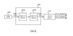
圖4係描繪根據一數位濾波器之一些實施方案之包含至少兩個級聯MA濾波器404a及404b之一低通濾波器400之一實例之一框圖。在此實例中,自CDR 408輸出之一相位控制信號首先由MA濾波器404a平滑,然後由MA濾波器404b平滑。在此實例中,MA濾波器404b之輸出被提供至一二進位至溫度計(binary-to-thermometer) 412,以用於二進位至溫度計解碼,然後被遞送至另一組件,諸如一PI。在此實例中,兩個MA濾波器都根據先前之公式操作,即:4 is a block diagram depicting an example of a low-
OUT(n) = OUT(n-1) + 1/N(P(n) - P(n-N)),其中:OUT(n) = OUT(n-1) + 1/N(P(n) - P(n-N)), where:
OUT(n)係輸出資料;OUT(n) is the output data;
P(n)係經採樣輸入資料,例如,自一CDR輸出以控制一PI之相位控制信號之一相位控制碼序列;且P(n) is the sampled input data, e.g., a phase control code sequence output from a CDR to control the phase control signal of a PI; and
n = 0, 1, 2,…。n = 0, 1, 2,....
然而,在圖4之實例中,以繪示之方式,MA濾波器404a支持N=8、16、32及64,而MA濾波器404b支持N=4。在其他實例中,針對MA濾波器404a及404b中之任一或兩者,N可為2、4、8、16、32、64、128、256或512。However, in the example of FIG. 4, by way of illustration,
圖5係描繪根據一些實施方案執行之一重計時方法500之一實例之一流程圖。在圖5中,重計時方法500包含:在504處,一CDR自與一接收器相關聯之一輸入資料信號提取一資料分量,如上文所描述的。在508處,例如藉由一FIFO將資料分量自CDR提供至發射器,如上文所描述的。在512處,CDR產生一相位控制信號,如上文所描述的。在一些實施方案中,在516處,併入一數位濾波器以接收並執行相位控制信號之數位濾波,以移除或減少與抖動雜訊相關聯之一或多個頻率分量。在520處,一相位內插器自數位濾波器接收相位控制信號,並基於相位控制信號產生一輸出時脈信號。在524處,相位內插器將輸出時脈信號提供至發射器以追蹤資料分量之資料封包。FIG. 5 depicts a flowchart of an example of a
所屬領域之技術人員將理解,可在不脫離本發明之範疇之情況下對本文所描述之實施方案之形式及細節進行改變。另外,儘管已參考各種實施方案描述各種優點、態樣及物件,但本發明之範疇不應受到此等優點、態樣及物件之限制。確切言之,應參考隨附發明申請專利範圍判定本發明之範疇。Those skilled in the art will understand that changes may be made in form and detail of the embodiments described herein without departing from the scope of the invention. In addition, although various advantages, aspects and objects have been described with reference to various embodiments, the scope of the present invention should not be limited by these advantages, aspects and objects. To be precise, the scope of the present invention should be judged with reference to the scope of claims of the attached invention application.
100:串列介面通信系統/串列匯流排通信系統/系統 102:上游裝置 104:下游裝置 106:串列匯流排 108:中繼器 200:重計時器 204:Tx埠 208:Rx埠 212:發射器(Tx) 216:接收器(Rx) 220:連續時間線性等化器(CTLE) 224:類比至數位轉換器(ADC) 228:時脈資料恢復電路(CDR) 232:決策回饋等化器(DFE) 236:資料輸出 240:先進先出電路(FIFO) 244:第一相位內插器(PI) 246:PI控制輸出 248:第二相位內插器(PI) 252:數位濾波器 256:系統PLL 260:時脈輸出 300:移動平均濾波器 304:m位元移位電路 308:m位元移位電路 312a至312N:延遲單元 316:第一加法器 320:第二加法器 324:延遲單元 400:低通濾波器 404a,404b:移動平均濾波器 408:時脈資料恢復電路(CDR) 412:二進位至溫度計 500:重計時方法 504:步驟 508:步驟 512:步驟 516:步驟 520:步驟 524:步驟100: serial interface communication system/serial bus communication system/system 102: Upstream device 104: Downstream device 106: serial bus 108: Repeater 200: Retimer 204:Tx port 208: Rx port 212: Transmitter (Tx) 216: Receiver (Rx) 220: Continuous Time Linear Equalizer (CTLE) 224: Analog to Digital Converter (ADC) 228: Clock data recovery circuit (CDR) 232: Decision Feedback Equalizer (DFE) 236: Data output 240: First in first out circuit (FIFO) 244: first phase interpolator (PI) 246: PI control output 248: second phase interpolator (PI) 252: digital filter 256: System PLL 260: clock output 300:Moving average filter 304: m-bit shift circuit 308: m-
圖1A係描繪呈一串列介面通信系統100形式之一資料傳輸系統之一實例之一框圖。FIG. 1A is a block diagram depicting an example of a data transmission system in the form of a serial
圖1B係描繪系統100之一些實施方案之一實例之一框圖,其中一匯流排包含一或多個中繼器108。FIG. 1B is a block diagram depicting an example of one of some implementations of a
圖2係描繪根據一些實施方案之一重計時器200之一實例之一框圖。FIG. 2 is a block diagram depicting an example of a re-timer 200 according to some implementations.
圖3係描繪根據一數位濾波器之一些實施方案之一移動平均濾波器300之一實例之一框圖。3 is a block diagram depicting an example of a moving
圖4係描繪根據一數位濾波器之一些實施方案之包含至少兩個移動平均濾波器404a及404b之一低通濾波器400之一實例之一框圖。4 is a block diagram depicting an example of a low-
圖5係描繪根據一些實施方案執行之一重計時方法500之一實例之一流程圖。FIG. 5 depicts a flowchart of an example of a
200:重計時器200: Retimer
204:Tx埠204:Tx port
208:Rx埠208: Rx port
212:發射器(Tx)212: Transmitter (Tx)
216:接收器(Rx)216: Receiver (Rx)
220:連續時間線性等化器(CTLE)220: Continuous Time Linear Equalizer (CTLE)
224:類比至數位轉換器(ADC)224: Analog to Digital Converter (ADC)
228:時脈資料恢復電路(CDR)228: Clock data recovery circuit (CDR)
232:決策回饋等化器(DFE)232: Decision Feedback Equalizer (DFE)
236:資料輸出236: Data output
240:先進先出電路(FIFO)240: First in first out circuit (FIFO)
244:第一相位內插器(PI)244: first phase interpolator (PI)
246:PI控制輸出246: PI control output
248:第二相位內插器(PI)248: second phase interpolator (PI)
252:數位濾波器252: digital filter
256:系統PLL256: System PLL
260:時脈輸出260: clock output
Claims (12)
Translated fromChineseApplications Claiming Priority (2)
| Application Number | Priority Date | Filing Date | Title |
|---|---|---|---|
| US17/451,563US11489657B1 (en) | 2021-10-20 | 2021-10-20 | Bit-level mode retimer |
| US17/451,563 | 2021-10-20 |
Publications (2)
| Publication Number | Publication Date |
|---|---|
| TW202324963Atrue TW202324963A (en) | 2023-06-16 |
| TWI828540B TWI828540B (en) | 2024-01-01 |
Family
ID=83809430
Family Applications (2)
| Application Number | Title | Priority Date | Filing Date |
|---|---|---|---|
| TW112105262ATWI828540B (en) | 2021-10-20 | 2022-06-08 | Phase interpolator circuitry for a bit-level mode retimer |
| TW111121140ATWI809923B (en) | 2021-10-20 | 2022-06-08 | Bit-level mode retimer |
Family Applications After (1)
| Application Number | Title | Priority Date | Filing Date |
|---|---|---|---|
| TW111121140ATWI809923B (en) | 2021-10-20 | 2022-06-08 | Bit-level mode retimer |
Country Status (4)
| Country | Link |
|---|---|
| US (2) | US11489657B1 (en) |
| KR (1) | KR20230056605A (en) |
| CN (2) | CN119628813A (en) |
| TW (2) | TWI828540B (en) |
Families Citing this family (5)
| Publication number | Priority date | Publication date | Assignee | Title |
|---|---|---|---|---|
| US12028079B2 (en)* | 2022-05-23 | 2024-07-02 | Texas Instruments Incorporated | Methods and apparatus to retime data using a programmable delay |
| US11902059B2 (en)* | 2022-05-27 | 2024-02-13 | Apple Inc. | Analog channel equalization and channel adaptation |
| US12176907B2 (en)* | 2022-12-27 | 2024-12-24 | Avago Technologies International Sales Pte. Limited | Systems for and methods of jitter reduction |
| KR20240172878A (en)* | 2023-06-02 | 2024-12-10 | 삼성전자주식회사 | Receiver including high speed decision feedback equalizer, communication system and operating method thereof |
| US20250274259A1 (en)* | 2024-02-28 | 2025-08-28 | Credo Technology Group Limited | Dual path clock forwarding |
Family Cites Families (21)
| Publication number | Priority date | Publication date | Assignee | Title |
|---|---|---|---|---|
| US6397042B1 (en)* | 1998-03-06 | 2002-05-28 | Texas Instruments Incorporated | Self test of an electronic device |
| US7664204B1 (en)* | 2005-03-10 | 2010-02-16 | Marvell International Ltd. | Adaptive timing using clock recovery |
| US7672417B2 (en)* | 2006-08-31 | 2010-03-02 | Montage Technology Group Limited | Clock and data recovery |
| US9444615B2 (en)* | 2011-07-25 | 2016-09-13 | Semtech Canada Corporation | Low latency digital jitter termination for repeater circuits |
| BR112014024483A8 (en)* | 2012-04-19 | 2021-05-25 | Intel Corp | input/output receiver and system |
| US8873606B2 (en)* | 2012-11-07 | 2014-10-28 | Broadcom Corporation | Transceiver including a high latency communication channel and a low latency communication channel |
| US20140281071A1 (en)* | 2013-03-15 | 2014-09-18 | Jianping Jane Xu | Optical memory extension architecture |
| US9444438B2 (en)* | 2013-06-10 | 2016-09-13 | Stmicroelectronics S.R.L. | Frequency doubler and related method of generating an oscillating voltage |
| US9091711B1 (en)* | 2013-07-18 | 2015-07-28 | Pmc-Sierra Us, Inc. | Wide-range fast-lock frequency acquisition for clock and data recovery |
| US9325489B2 (en)* | 2013-12-19 | 2016-04-26 | Xilinx, Inc. | Data receivers and methods of implementing data receivers in an integrated circuit |
| TWI519119B (en)* | 2014-04-17 | 2016-01-21 | 創意電子股份有限公司 | Clock data recovery circuit and method |
| KR20160069093A (en)* | 2014-12-05 | 2016-06-16 | 에스케이하이닉스 주식회사 | Clock and data recovery circuit and system using the same |
| WO2017189796A1 (en)* | 2016-04-29 | 2017-11-02 | Megachips Technology America Corporation | Data transmission method and data transmission system |
| CN107864104B (en)* | 2016-09-21 | 2020-07-10 | 联发科技股份有限公司 | Digital signal processing method and electronic device |
| CN108599915A (en)* | 2018-03-12 | 2018-09-28 | 北京理工大学 | Based on number between the send-receive clock of closed loop phase ambiguity estimation and compensation method |
| US10484167B2 (en)* | 2018-03-13 | 2019-11-19 | Xilinx, Inc. | Circuit for and method of receiving a signal in an integrated circuit device |
| CN112840593B (en)* | 2018-12-21 | 2022-05-13 | 华为技术有限公司 | Clock domain crossing processing circuit |
| US11108401B2 (en)* | 2019-11-19 | 2021-08-31 | Xilinx, Inc. | Low noise quadrature signal generation |
| US11070224B1 (en)* | 2020-05-07 | 2021-07-20 | Mellanox Technologies, Ltd. | Method and apparatus for implementing multirate SerDes systems |
| CN113972910B (en)* | 2020-07-24 | 2025-07-04 | 瑞昱半导体股份有限公司 | Frequency control device and frequency control method |
| US10979258B1 (en)* | 2020-10-15 | 2021-04-13 | Parade Technologies, Ltd. | Seamless bit-level low-latency retimer for data links |
- 2021
- 2021-10-20USUS17/451,563patent/US11489657B1/enactiveActive
- 2022
- 2022-06-08TWTW112105262Apatent/TWI828540B/enactive
- 2022-06-08TWTW111121140Apatent/TWI809923B/enactive
- 2022-06-15CNCN202411689857.9Apatent/CN119628813A/enactivePending
- 2022-06-15CNCN202210677397.2Apatent/CN115996110B/enactiveActive
- 2022-09-27USUS17/935,618patent/US11736266B2/enactiveActive
- 2022-10-18KRKR1020220134308Apatent/KR20230056605A/enactivePending
Also Published As
| Publication number | Publication date |
|---|---|
| CN115996110A (en) | 2023-04-21 |
| US11489657B1 (en) | 2022-11-01 |
| US11736266B2 (en) | 2023-08-22 |
| TWI809923B (en) | 2023-07-21 |
| CN119628813A (en) | 2025-03-14 |
| TW202318830A (en) | 2023-05-01 |
| US20230122556A1 (en) | 2023-04-20 |
| TWI828540B (en) | 2024-01-01 |
| CN115996110B (en) | 2024-12-17 |
| KR20230056605A (en) | 2023-04-27 |
Similar Documents
| Publication | Publication Date | Title |
|---|---|---|
| TWI809923B (en) | Bit-level mode retimer | |
| US10148414B2 (en) | Deskew in a high speed link | |
| CN113676309B (en) | Second order clock recovery using three feedback paths | |
| CN106470177B (en) | CDR apparatus, receiver and method for shifting with DFE | |
| JP4956840B2 (en) | Judgment feedback equalization apparatus and method | |
| US9071479B2 (en) | High-speed parallel decision feedback equalizer | |
| US8654898B2 (en) | Digital equalizer for high-speed serial communications | |
| US8301036B2 (en) | High-speed adaptive decision feedback equalizer | |
| US7924912B1 (en) | Method and apparatus for a unified signaling decision feedback equalizer | |
| CN110858824B (en) | Pre-compensator based quantization for clock recovery | |
| US10728059B1 (en) | Parallel mixed-signal equalization for high-speed serial link | |
| US7447278B2 (en) | Apparatus for transmitting and receiving data | |
| WO2018067666A1 (en) | Reduced complexity precomputation for decision feedback equalizer | |
| Zhang et al. | PAM4 signaling for 56G serial link applications—A tutorial | |
| US7668238B1 (en) | Method and apparatus for a high speed decision feedback equalizer | |
| US11231740B2 (en) | Clock recovery using between-interval timing error estimation | |
| US11831475B1 (en) | Receiver using pseudo partial response maximum likelihood sequence detection | |
| Morgan et al. | A comparison of 25 Gbps NRZ & PAM-4 modulation used in reference, legacy, & premium backplane channels | |
| Ramamoorthy et al. | High speed serial link transmitter for 10Gig ethernet applications | |
| Ting | A Blind Baud-rate CDR and Zero-forcing Adaptive DFE for an ADC-based Receiver | |
| Aziz et al. | SerDes Design and Modeling over 25+ Gb/s Serial Link |