TW202314988A - Semiconductor package - Google Patents
Semiconductor packageDownload PDFInfo
- Publication number
- TW202314988A TW202314988ATW111131663ATW111131663ATW202314988ATW 202314988 ATW202314988 ATW 202314988ATW 111131663 ATW111131663 ATW 111131663ATW 111131663 ATW111131663 ATW 111131663ATW 202314988 ATW202314988 ATW 202314988A
- Authority
- TW
- Taiwan
- Prior art keywords
- semiconductor
- pad
- pads
- connection terminal
- pad group
- Prior art date
Links
Images


Classifications
- H—ELECTRICITY
- H01—ELECTRIC ELEMENTS
- H01L—SEMICONDUCTOR DEVICES NOT COVERED BY CLASS H10
- H01L23/00—Details of semiconductor or other solid state devices
- H01L23/48—Arrangements for conducting electric current to or from the solid state body in operation, e.g. leads, terminal arrangements ; Selection of materials therefor
- H01L23/481—Internal lead connections, e.g. via connections, feedthrough structures
- H—ELECTRICITY
- H01—ELECTRIC ELEMENTS
- H01L—SEMICONDUCTOR DEVICES NOT COVERED BY CLASS H10
- H01L24/00—Arrangements for connecting or disconnecting semiconductor or solid-state bodies; Methods or apparatus related thereto
- H01L24/01—Means for bonding being attached to, or being formed on, the surface to be connected, e.g. chip-to-package, die-attach, "first-level" interconnects; Manufacturing methods related thereto
- H01L24/10—Bump connectors ; Manufacturing methods related thereto
- H01L24/15—Structure, shape, material or disposition of the bump connectors after the connecting process
- H01L24/16—Structure, shape, material or disposition of the bump connectors after the connecting process of an individual bump connector
- H—ELECTRICITY
- H01—ELECTRIC ELEMENTS
- H01L—SEMICONDUCTOR DEVICES NOT COVERED BY CLASS H10
- H01L24/00—Arrangements for connecting or disconnecting semiconductor or solid-state bodies; Methods or apparatus related thereto
- H01L24/01—Means for bonding being attached to, or being formed on, the surface to be connected, e.g. chip-to-package, die-attach, "first-level" interconnects; Manufacturing methods related thereto
- H01L24/10—Bump connectors ; Manufacturing methods related thereto
- H01L24/15—Structure, shape, material or disposition of the bump connectors after the connecting process
- H01L24/17—Structure, shape, material or disposition of the bump connectors after the connecting process of a plurality of bump connectors
- H—ELECTRICITY
- H01—ELECTRIC ELEMENTS
- H01L—SEMICONDUCTOR DEVICES NOT COVERED BY CLASS H10
- H01L23/00—Details of semiconductor or other solid state devices
- H01L23/48—Arrangements for conducting electric current to or from the solid state body in operation, e.g. leads, terminal arrangements ; Selection of materials therefor
- H01L23/482—Arrangements for conducting electric current to or from the solid state body in operation, e.g. leads, terminal arrangements ; Selection of materials therefor consisting of lead-in layers inseparably applied to the semiconductor body (electrodes)
- H01L23/485—Arrangements for conducting electric current to or from the solid state body in operation, e.g. leads, terminal arrangements ; Selection of materials therefor consisting of lead-in layers inseparably applied to the semiconductor body (electrodes) consisting of layered constructions comprising conductive layers and insulating layers, e.g. planar contacts
- H—ELECTRICITY
- H01—ELECTRIC ELEMENTS
- H01L—SEMICONDUCTOR DEVICES NOT COVERED BY CLASS H10
- H01L24/00—Arrangements for connecting or disconnecting semiconductor or solid-state bodies; Methods or apparatus related thereto
- H01L24/01—Means for bonding being attached to, or being formed on, the surface to be connected, e.g. chip-to-package, die-attach, "first-level" interconnects; Manufacturing methods related thereto
- H01L24/02—Bonding areas ; Manufacturing methods related thereto
- H01L24/04—Structure, shape, material or disposition of the bonding areas prior to the connecting process
- H01L24/06—Structure, shape, material or disposition of the bonding areas prior to the connecting process of a plurality of bonding areas
- H—ELECTRICITY
- H01—ELECTRIC ELEMENTS
- H01L—SEMICONDUCTOR DEVICES NOT COVERED BY CLASS H10
- H01L24/00—Arrangements for connecting or disconnecting semiconductor or solid-state bodies; Methods or apparatus related thereto
- H01L24/01—Means for bonding being attached to, or being formed on, the surface to be connected, e.g. chip-to-package, die-attach, "first-level" interconnects; Manufacturing methods related thereto
- H01L24/02—Bonding areas ; Manufacturing methods related thereto
- H01L24/07—Structure, shape, material or disposition of the bonding areas after the connecting process
- H01L24/08—Structure, shape, material or disposition of the bonding areas after the connecting process of an individual bonding area
- H—ELECTRICITY
- H01—ELECTRIC ELEMENTS
- H01L—SEMICONDUCTOR DEVICES NOT COVERED BY CLASS H10
- H01L24/00—Arrangements for connecting or disconnecting semiconductor or solid-state bodies; Methods or apparatus related thereto
- H01L24/01—Means for bonding being attached to, or being formed on, the surface to be connected, e.g. chip-to-package, die-attach, "first-level" interconnects; Manufacturing methods related thereto
- H01L24/02—Bonding areas ; Manufacturing methods related thereto
- H01L24/07—Structure, shape, material or disposition of the bonding areas after the connecting process
- H01L24/09—Structure, shape, material or disposition of the bonding areas after the connecting process of a plurality of bonding areas
- H—ELECTRICITY
- H01—ELECTRIC ELEMENTS
- H01L—SEMICONDUCTOR DEVICES NOT COVERED BY CLASS H10
- H01L24/00—Arrangements for connecting or disconnecting semiconductor or solid-state bodies; Methods or apparatus related thereto
- H01L24/01—Means for bonding being attached to, or being formed on, the surface to be connected, e.g. chip-to-package, die-attach, "first-level" interconnects; Manufacturing methods related thereto
- H01L24/18—High density interconnect [HDI] connectors; Manufacturing methods related thereto
- H01L24/23—Structure, shape, material or disposition of the high density interconnect connectors after the connecting process
- H01L24/24—Structure, shape, material or disposition of the high density interconnect connectors after the connecting process of an individual high density interconnect connector
- H—ELECTRICITY
- H01—ELECTRIC ELEMENTS
- H01L—SEMICONDUCTOR DEVICES NOT COVERED BY CLASS H10
- H01L25/00—Assemblies consisting of a plurality of semiconductor or other solid state devices
- H01L25/03—Assemblies consisting of a plurality of semiconductor or other solid state devices all the devices being of a type provided for in a single subclass of subclasses H10B, H10D, H10F, H10H, H10K or H10N, e.g. assemblies of rectifier diodes
- H01L25/04—Assemblies consisting of a plurality of semiconductor or other solid state devices all the devices being of a type provided for in a single subclass of subclasses H10B, H10D, H10F, H10H, H10K or H10N, e.g. assemblies of rectifier diodes the devices not having separate containers
- H01L25/065—Assemblies consisting of a plurality of semiconductor or other solid state devices all the devices being of a type provided for in a single subclass of subclasses H10B, H10D, H10F, H10H, H10K or H10N, e.g. assemblies of rectifier diodes the devices not having separate containers the devices being of a type provided for in group H10D89/00
- H01L25/0652—Assemblies consisting of a plurality of semiconductor or other solid state devices all the devices being of a type provided for in a single subclass of subclasses H10B, H10D, H10F, H10H, H10K or H10N, e.g. assemblies of rectifier diodes the devices not having separate containers the devices being of a type provided for in group H10D89/00 the devices being arranged next and on each other, i.e. mixed assemblies
- H—ELECTRICITY
- H01—ELECTRIC ELEMENTS
- H01L—SEMICONDUCTOR DEVICES NOT COVERED BY CLASS H10
- H01L25/00—Assemblies consisting of a plurality of semiconductor or other solid state devices
- H01L25/03—Assemblies consisting of a plurality of semiconductor or other solid state devices all the devices being of a type provided for in a single subclass of subclasses H10B, H10D, H10F, H10H, H10K or H10N, e.g. assemblies of rectifier diodes
- H01L25/04—Assemblies consisting of a plurality of semiconductor or other solid state devices all the devices being of a type provided for in a single subclass of subclasses H10B, H10D, H10F, H10H, H10K or H10N, e.g. assemblies of rectifier diodes the devices not having separate containers
- H01L25/065—Assemblies consisting of a plurality of semiconductor or other solid state devices all the devices being of a type provided for in a single subclass of subclasses H10B, H10D, H10F, H10H, H10K or H10N, e.g. assemblies of rectifier diodes the devices not having separate containers the devices being of a type provided for in group H10D89/00
- H01L25/0657—Stacked arrangements of devices
- H—ELECTRICITY
- H01—ELECTRIC ELEMENTS
- H01L—SEMICONDUCTOR DEVICES NOT COVERED BY CLASS H10
- H01L2224/00—Indexing scheme for arrangements for connecting or disconnecting semiconductor or solid-state bodies and methods related thereto as covered by H01L24/00
- H01L2224/01—Means for bonding being attached to, or being formed on, the surface to be connected, e.g. chip-to-package, die-attach, "first-level" interconnects; Manufacturing methods related thereto
- H01L2224/02—Bonding areas; Manufacturing methods related thereto
- H01L2224/04—Structure, shape, material or disposition of the bonding areas prior to the connecting process
- H01L2224/0401—Bonding areas specifically adapted for bump connectors, e.g. under bump metallisation [UBM]
- H—ELECTRICITY
- H01—ELECTRIC ELEMENTS
- H01L—SEMICONDUCTOR DEVICES NOT COVERED BY CLASS H10
- H01L2224/00—Indexing scheme for arrangements for connecting or disconnecting semiconductor or solid-state bodies and methods related thereto as covered by H01L24/00
- H01L2224/01—Means for bonding being attached to, or being formed on, the surface to be connected, e.g. chip-to-package, die-attach, "first-level" interconnects; Manufacturing methods related thereto
- H01L2224/02—Bonding areas; Manufacturing methods related thereto
- H01L2224/04—Structure, shape, material or disposition of the bonding areas prior to the connecting process
- H01L2224/05—Structure, shape, material or disposition of the bonding areas prior to the connecting process of an individual bonding area
- H01L2224/0554—External layer
- H01L2224/0556—Disposition
- H01L2224/0557—Disposition the external layer being disposed on a via connection of the semiconductor or solid-state body
- H—ELECTRICITY
- H01—ELECTRIC ELEMENTS
- H01L—SEMICONDUCTOR DEVICES NOT COVERED BY CLASS H10
- H01L2224/00—Indexing scheme for arrangements for connecting or disconnecting semiconductor or solid-state bodies and methods related thereto as covered by H01L24/00
- H01L2224/01—Means for bonding being attached to, or being formed on, the surface to be connected, e.g. chip-to-package, die-attach, "first-level" interconnects; Manufacturing methods related thereto
- H01L2224/02—Bonding areas; Manufacturing methods related thereto
- H01L2224/04—Structure, shape, material or disposition of the bonding areas prior to the connecting process
- H01L2224/06—Structure, shape, material or disposition of the bonding areas prior to the connecting process of a plurality of bonding areas
- H01L2224/0601—Structure
- H01L2224/0603—Bonding areas having different sizes, e.g. different heights or widths
- H—ELECTRICITY
- H01—ELECTRIC ELEMENTS
- H01L—SEMICONDUCTOR DEVICES NOT COVERED BY CLASS H10
- H01L2224/00—Indexing scheme for arrangements for connecting or disconnecting semiconductor or solid-state bodies and methods related thereto as covered by H01L24/00
- H01L2224/01—Means for bonding being attached to, or being formed on, the surface to be connected, e.g. chip-to-package, die-attach, "first-level" interconnects; Manufacturing methods related thereto
- H01L2224/02—Bonding areas; Manufacturing methods related thereto
- H01L2224/04—Structure, shape, material or disposition of the bonding areas prior to the connecting process
- H01L2224/06—Structure, shape, material or disposition of the bonding areas prior to the connecting process of a plurality of bonding areas
- H01L2224/061—Disposition
- H01L2224/0618—Disposition being disposed on at least two different sides of the body, e.g. dual array
- H01L2224/06181—On opposite sides of the body
- H—ELECTRICITY
- H01—ELECTRIC ELEMENTS
- H01L—SEMICONDUCTOR DEVICES NOT COVERED BY CLASS H10
- H01L2224/00—Indexing scheme for arrangements for connecting or disconnecting semiconductor or solid-state bodies and methods related thereto as covered by H01L24/00
- H01L2224/01—Means for bonding being attached to, or being formed on, the surface to be connected, e.g. chip-to-package, die-attach, "first-level" interconnects; Manufacturing methods related thereto
- H01L2224/02—Bonding areas; Manufacturing methods related thereto
- H01L2224/04—Structure, shape, material or disposition of the bonding areas prior to the connecting process
- H01L2224/06—Structure, shape, material or disposition of the bonding areas prior to the connecting process of a plurality of bonding areas
- H01L2224/0651—Function
- H01L2224/06515—Bonding areas having different functions
- H01L2224/06517—Bonding areas having different functions including bonding areas providing primarily mechanical bonding
- H—ELECTRICITY
- H01—ELECTRIC ELEMENTS
- H01L—SEMICONDUCTOR DEVICES NOT COVERED BY CLASS H10
- H01L2224/00—Indexing scheme for arrangements for connecting or disconnecting semiconductor or solid-state bodies and methods related thereto as covered by H01L24/00
- H01L2224/01—Means for bonding being attached to, or being formed on, the surface to be connected, e.g. chip-to-package, die-attach, "first-level" interconnects; Manufacturing methods related thereto
- H01L2224/02—Bonding areas; Manufacturing methods related thereto
- H01L2224/07—Structure, shape, material or disposition of the bonding areas after the connecting process
- H01L2224/08—Structure, shape, material or disposition of the bonding areas after the connecting process of an individual bonding area
- H01L2224/0801—Structure
- H—ELECTRICITY
- H01—ELECTRIC ELEMENTS
- H01L—SEMICONDUCTOR DEVICES NOT COVERED BY CLASS H10
- H01L2224/00—Indexing scheme for arrangements for connecting or disconnecting semiconductor or solid-state bodies and methods related thereto as covered by H01L24/00
- H01L2224/01—Means for bonding being attached to, or being formed on, the surface to be connected, e.g. chip-to-package, die-attach, "first-level" interconnects; Manufacturing methods related thereto
- H01L2224/02—Bonding areas; Manufacturing methods related thereto
- H01L2224/07—Structure, shape, material or disposition of the bonding areas after the connecting process
- H01L2224/08—Structure, shape, material or disposition of the bonding areas after the connecting process of an individual bonding area
- H01L2224/0805—Shape
- H01L2224/08057—Shape in side view
- H01L2224/08058—Shape in side view being non uniform along the bonding area
- H—ELECTRICITY
- H01—ELECTRIC ELEMENTS
- H01L—SEMICONDUCTOR DEVICES NOT COVERED BY CLASS H10
- H01L2224/00—Indexing scheme for arrangements for connecting or disconnecting semiconductor or solid-state bodies and methods related thereto as covered by H01L24/00
- H01L2224/01—Means for bonding being attached to, or being formed on, the surface to be connected, e.g. chip-to-package, die-attach, "first-level" interconnects; Manufacturing methods related thereto
- H01L2224/02—Bonding areas; Manufacturing methods related thereto
- H01L2224/07—Structure, shape, material or disposition of the bonding areas after the connecting process
- H01L2224/08—Structure, shape, material or disposition of the bonding areas after the connecting process of an individual bonding area
- H01L2224/081—Disposition
- H01L2224/0812—Disposition the bonding area connecting directly to another bonding area, i.e. connectorless bonding, e.g. bumpless bonding
- H01L2224/08135—Disposition the bonding area connecting directly to another bonding area, i.e. connectorless bonding, e.g. bumpless bonding the bonding area connecting between different semiconductor or solid-state bodies, i.e. chip-to-chip
- H01L2224/08145—Disposition the bonding area connecting directly to another bonding area, i.e. connectorless bonding, e.g. bumpless bonding the bonding area connecting between different semiconductor or solid-state bodies, i.e. chip-to-chip the bodies being stacked
- H01L2224/08148—Disposition the bonding area connecting directly to another bonding area, i.e. connectorless bonding, e.g. bumpless bonding the bonding area connecting between different semiconductor or solid-state bodies, i.e. chip-to-chip the bodies being stacked the bonding area connecting to a bonding area protruding from the surface of the body
- H—ELECTRICITY
- H01—ELECTRIC ELEMENTS
- H01L—SEMICONDUCTOR DEVICES NOT COVERED BY CLASS H10
- H01L2224/00—Indexing scheme for arrangements for connecting or disconnecting semiconductor or solid-state bodies and methods related thereto as covered by H01L24/00
- H01L2224/01—Means for bonding being attached to, or being formed on, the surface to be connected, e.g. chip-to-package, die-attach, "first-level" interconnects; Manufacturing methods related thereto
- H01L2224/02—Bonding areas; Manufacturing methods related thereto
- H01L2224/07—Structure, shape, material or disposition of the bonding areas after the connecting process
- H01L2224/09—Structure, shape, material or disposition of the bonding areas after the connecting process of a plurality of bonding areas
- H01L2224/0901—Structure
- H01L2224/0903—Bonding areas having different sizes, e.g. different diameters, heights or widths
- H—ELECTRICITY
- H01—ELECTRIC ELEMENTS
- H01L—SEMICONDUCTOR DEVICES NOT COVERED BY CLASS H10
- H01L2224/00—Indexing scheme for arrangements for connecting or disconnecting semiconductor or solid-state bodies and methods related thereto as covered by H01L24/00
- H01L2224/01—Means for bonding being attached to, or being formed on, the surface to be connected, e.g. chip-to-package, die-attach, "first-level" interconnects; Manufacturing methods related thereto
- H01L2224/02—Bonding areas; Manufacturing methods related thereto
- H01L2224/07—Structure, shape, material or disposition of the bonding areas after the connecting process
- H01L2224/09—Structure, shape, material or disposition of the bonding areas after the connecting process of a plurality of bonding areas
- H01L2224/091—Disposition
- H01L2224/0912—Layout
- H01L2224/0913—Square or rectangular array
- H01L2224/09132—Square or rectangular array being non uniform, i.e. having a non uniform pitch across the array
- H—ELECTRICITY
- H01—ELECTRIC ELEMENTS
- H01L—SEMICONDUCTOR DEVICES NOT COVERED BY CLASS H10
- H01L2224/00—Indexing scheme for arrangements for connecting or disconnecting semiconductor or solid-state bodies and methods related thereto as covered by H01L24/00
- H01L2224/01—Means for bonding being attached to, or being formed on, the surface to be connected, e.g. chip-to-package, die-attach, "first-level" interconnects; Manufacturing methods related thereto
- H01L2224/02—Bonding areas; Manufacturing methods related thereto
- H01L2224/07—Structure, shape, material or disposition of the bonding areas after the connecting process
- H01L2224/09—Structure, shape, material or disposition of the bonding areas after the connecting process of a plurality of bonding areas
- H01L2224/091—Disposition
- H01L2224/0912—Layout
- H01L2224/0913—Square or rectangular array
- H01L2224/09133—Square or rectangular array with a staggered arrangement, e.g. depopulated array
- H—ELECTRICITY
- H01—ELECTRIC ELEMENTS
- H01L—SEMICONDUCTOR DEVICES NOT COVERED BY CLASS H10
- H01L2224/00—Indexing scheme for arrangements for connecting or disconnecting semiconductor or solid-state bodies and methods related thereto as covered by H01L24/00
- H01L2224/01—Means for bonding being attached to, or being formed on, the surface to be connected, e.g. chip-to-package, die-attach, "first-level" interconnects; Manufacturing methods related thereto
- H01L2224/10—Bump connectors; Manufacturing methods related thereto
- H01L2224/12—Structure, shape, material or disposition of the bump connectors prior to the connecting process
- H01L2224/13—Structure, shape, material or disposition of the bump connectors prior to the connecting process of an individual bump connector
- H01L2224/13001—Core members of the bump connector
- H01L2224/1302—Disposition
- H01L2224/13025—Disposition the bump connector being disposed on a via connection of the semiconductor or solid-state body
- H—ELECTRICITY
- H01—ELECTRIC ELEMENTS
- H01L—SEMICONDUCTOR DEVICES NOT COVERED BY CLASS H10
- H01L2224/00—Indexing scheme for arrangements for connecting or disconnecting semiconductor or solid-state bodies and methods related thereto as covered by H01L24/00
- H01L2224/01—Means for bonding being attached to, or being formed on, the surface to be connected, e.g. chip-to-package, die-attach, "first-level" interconnects; Manufacturing methods related thereto
- H01L2224/10—Bump connectors; Manufacturing methods related thereto
- H01L2224/12—Structure, shape, material or disposition of the bump connectors prior to the connecting process
- H01L2224/14—Structure, shape, material or disposition of the bump connectors prior to the connecting process of a plurality of bump connectors
- H01L2224/141—Disposition
- H01L2224/1418—Disposition being disposed on at least two different sides of the body, e.g. dual array
- H01L2224/14181—On opposite sides of the body
- H—ELECTRICITY
- H01—ELECTRIC ELEMENTS
- H01L—SEMICONDUCTOR DEVICES NOT COVERED BY CLASS H10
- H01L2224/00—Indexing scheme for arrangements for connecting or disconnecting semiconductor or solid-state bodies and methods related thereto as covered by H01L24/00
- H01L2224/01—Means for bonding being attached to, or being formed on, the surface to be connected, e.g. chip-to-package, die-attach, "first-level" interconnects; Manufacturing methods related thereto
- H01L2224/10—Bump connectors; Manufacturing methods related thereto
- H01L2224/15—Structure, shape, material or disposition of the bump connectors after the connecting process
- H01L2224/16—Structure, shape, material or disposition of the bump connectors after the connecting process of an individual bump connector
- H01L2224/1601—Structure
- H01L2224/16012—Structure relative to the bonding area, e.g. bond pad
- H01L2224/16013—Structure relative to the bonding area, e.g. bond pad the bump connector being larger than the bonding area, e.g. bond pad
- H—ELECTRICITY
- H01—ELECTRIC ELEMENTS
- H01L—SEMICONDUCTOR DEVICES NOT COVERED BY CLASS H10
- H01L2224/00—Indexing scheme for arrangements for connecting or disconnecting semiconductor or solid-state bodies and methods related thereto as covered by H01L24/00
- H01L2224/01—Means for bonding being attached to, or being formed on, the surface to be connected, e.g. chip-to-package, die-attach, "first-level" interconnects; Manufacturing methods related thereto
- H01L2224/10—Bump connectors; Manufacturing methods related thereto
- H01L2224/15—Structure, shape, material or disposition of the bump connectors after the connecting process
- H01L2224/16—Structure, shape, material or disposition of the bump connectors after the connecting process of an individual bump connector
- H01L2224/1601—Structure
- H01L2224/16012—Structure relative to the bonding area, e.g. bond pad
- H01L2224/16014—Structure relative to the bonding area, e.g. bond pad the bump connector being smaller than the bonding area, e.g. bond pad
- H—ELECTRICITY
- H01—ELECTRIC ELEMENTS
- H01L—SEMICONDUCTOR DEVICES NOT COVERED BY CLASS H10
- H01L2224/00—Indexing scheme for arrangements for connecting or disconnecting semiconductor or solid-state bodies and methods related thereto as covered by H01L24/00
- H01L2224/01—Means for bonding being attached to, or being formed on, the surface to be connected, e.g. chip-to-package, die-attach, "first-level" interconnects; Manufacturing methods related thereto
- H01L2224/10—Bump connectors; Manufacturing methods related thereto
- H01L2224/15—Structure, shape, material or disposition of the bump connectors after the connecting process
- H01L2224/16—Structure, shape, material or disposition of the bump connectors after the connecting process of an individual bump connector
- H01L2224/1605—Shape
- H01L2224/16052—Shape in top view
- H01L2224/16055—Shape in top view being circular or elliptic
- H—ELECTRICITY
- H01—ELECTRIC ELEMENTS
- H01L—SEMICONDUCTOR DEVICES NOT COVERED BY CLASS H10
- H01L2224/00—Indexing scheme for arrangements for connecting or disconnecting semiconductor or solid-state bodies and methods related thereto as covered by H01L24/00
- H01L2224/01—Means for bonding being attached to, or being formed on, the surface to be connected, e.g. chip-to-package, die-attach, "first-level" interconnects; Manufacturing methods related thereto
- H01L2224/10—Bump connectors; Manufacturing methods related thereto
- H01L2224/15—Structure, shape, material or disposition of the bump connectors after the connecting process
- H01L2224/16—Structure, shape, material or disposition of the bump connectors after the connecting process of an individual bump connector
- H01L2224/1605—Shape
- H01L2224/16057—Shape in side view
- H01L2224/16059—Shape in side view comprising protrusions or indentations
- H—ELECTRICITY
- H01—ELECTRIC ELEMENTS
- H01L—SEMICONDUCTOR DEVICES NOT COVERED BY CLASS H10
- H01L2224/00—Indexing scheme for arrangements for connecting or disconnecting semiconductor or solid-state bodies and methods related thereto as covered by H01L24/00
- H01L2224/01—Means for bonding being attached to, or being formed on, the surface to be connected, e.g. chip-to-package, die-attach, "first-level" interconnects; Manufacturing methods related thereto
- H01L2224/10—Bump connectors; Manufacturing methods related thereto
- H01L2224/15—Structure, shape, material or disposition of the bump connectors after the connecting process
- H01L2224/16—Structure, shape, material or disposition of the bump connectors after the connecting process of an individual bump connector
- H01L2224/1605—Shape
- H01L2224/1607—Shape of bonding interfaces, e.g. interlocking features
- H—ELECTRICITY
- H01—ELECTRIC ELEMENTS
- H01L—SEMICONDUCTOR DEVICES NOT COVERED BY CLASS H10
- H01L2224/00—Indexing scheme for arrangements for connecting or disconnecting semiconductor or solid-state bodies and methods related thereto as covered by H01L24/00
- H01L2224/01—Means for bonding being attached to, or being formed on, the surface to be connected, e.g. chip-to-package, die-attach, "first-level" interconnects; Manufacturing methods related thereto
- H01L2224/10—Bump connectors; Manufacturing methods related thereto
- H01L2224/15—Structure, shape, material or disposition of the bump connectors after the connecting process
- H01L2224/16—Structure, shape, material or disposition of the bump connectors after the connecting process of an individual bump connector
- H01L2224/161—Disposition
- H01L2224/16135—Disposition the bump connector connecting between different semiconductor or solid-state bodies, i.e. chip-to-chip
- H01L2224/16145—Disposition the bump connector connecting between different semiconductor or solid-state bodies, i.e. chip-to-chip the bodies being stacked
- H01L2224/16146—Disposition the bump connector connecting between different semiconductor or solid-state bodies, i.e. chip-to-chip the bodies being stacked the bump connector connecting to a via connection in the semiconductor or solid-state body
- H—ELECTRICITY
- H01—ELECTRIC ELEMENTS
- H01L—SEMICONDUCTOR DEVICES NOT COVERED BY CLASS H10
- H01L2224/00—Indexing scheme for arrangements for connecting or disconnecting semiconductor or solid-state bodies and methods related thereto as covered by H01L24/00
- H01L2224/01—Means for bonding being attached to, or being formed on, the surface to be connected, e.g. chip-to-package, die-attach, "first-level" interconnects; Manufacturing methods related thereto
- H01L2224/10—Bump connectors; Manufacturing methods related thereto
- H01L2224/15—Structure, shape, material or disposition of the bump connectors after the connecting process
- H01L2224/16—Structure, shape, material or disposition of the bump connectors after the connecting process of an individual bump connector
- H01L2224/161—Disposition
- H01L2224/16135—Disposition the bump connector connecting between different semiconductor or solid-state bodies, i.e. chip-to-chip
- H01L2224/16145—Disposition the bump connector connecting between different semiconductor or solid-state bodies, i.e. chip-to-chip the bodies being stacked
- H01L2224/16148—Disposition the bump connector connecting between different semiconductor or solid-state bodies, i.e. chip-to-chip the bodies being stacked the bump connector connecting to a bonding area protruding from the surface
- H—ELECTRICITY
- H01—ELECTRIC ELEMENTS
- H01L—SEMICONDUCTOR DEVICES NOT COVERED BY CLASS H10
- H01L2224/00—Indexing scheme for arrangements for connecting or disconnecting semiconductor or solid-state bodies and methods related thereto as covered by H01L24/00
- H01L2224/01—Means for bonding being attached to, or being formed on, the surface to be connected, e.g. chip-to-package, die-attach, "first-level" interconnects; Manufacturing methods related thereto
- H01L2224/10—Bump connectors; Manufacturing methods related thereto
- H01L2224/15—Structure, shape, material or disposition of the bump connectors after the connecting process
- H01L2224/17—Structure, shape, material or disposition of the bump connectors after the connecting process of a plurality of bump connectors
- H01L2224/1701—Structure
- H01L2224/1703—Bump connectors having different sizes, e.g. different diameters, heights or widths
- H—ELECTRICITY
- H01—ELECTRIC ELEMENTS
- H01L—SEMICONDUCTOR DEVICES NOT COVERED BY CLASS H10
- H01L2224/00—Indexing scheme for arrangements for connecting or disconnecting semiconductor or solid-state bodies and methods related thereto as covered by H01L24/00
- H01L2224/01—Means for bonding being attached to, or being formed on, the surface to be connected, e.g. chip-to-package, die-attach, "first-level" interconnects; Manufacturing methods related thereto
- H01L2224/10—Bump connectors; Manufacturing methods related thereto
- H01L2224/15—Structure, shape, material or disposition of the bump connectors after the connecting process
- H01L2224/17—Structure, shape, material or disposition of the bump connectors after the connecting process of a plurality of bump connectors
- H01L2224/1705—Shape
- H01L2224/17051—Bump connectors having different shapes
- H01L2224/17055—Bump connectors having different shapes of their bonding interfaces
- H—ELECTRICITY
- H01—ELECTRIC ELEMENTS
- H01L—SEMICONDUCTOR DEVICES NOT COVERED BY CLASS H10
- H01L2224/00—Indexing scheme for arrangements for connecting or disconnecting semiconductor or solid-state bodies and methods related thereto as covered by H01L24/00
- H01L2224/01—Means for bonding being attached to, or being formed on, the surface to be connected, e.g. chip-to-package, die-attach, "first-level" interconnects; Manufacturing methods related thereto
- H01L2224/10—Bump connectors; Manufacturing methods related thereto
- H01L2224/15—Structure, shape, material or disposition of the bump connectors after the connecting process
- H01L2224/17—Structure, shape, material or disposition of the bump connectors after the connecting process of a plurality of bump connectors
- H01L2224/171—Disposition
- H01L2224/1712—Layout
- H01L2224/1713—Square or rectangular array
- H01L2224/17132—Square or rectangular array being non uniform, i.e. having a non uniform pitch across the array
- H—ELECTRICITY
- H01—ELECTRIC ELEMENTS
- H01L—SEMICONDUCTOR DEVICES NOT COVERED BY CLASS H10
- H01L2224/00—Indexing scheme for arrangements for connecting or disconnecting semiconductor or solid-state bodies and methods related thereto as covered by H01L24/00
- H01L2224/01—Means for bonding being attached to, or being formed on, the surface to be connected, e.g. chip-to-package, die-attach, "first-level" interconnects; Manufacturing methods related thereto
- H01L2224/10—Bump connectors; Manufacturing methods related thereto
- H01L2224/15—Structure, shape, material or disposition of the bump connectors after the connecting process
- H01L2224/17—Structure, shape, material or disposition of the bump connectors after the connecting process of a plurality of bump connectors
- H01L2224/171—Disposition
- H01L2224/1712—Layout
- H01L2224/1713—Square or rectangular array
- H01L2224/17133—Square or rectangular array with a staggered arrangement, e.g. depopulated array
- H—ELECTRICITY
- H01—ELECTRIC ELEMENTS
- H01L—SEMICONDUCTOR DEVICES NOT COVERED BY CLASS H10
- H01L2224/00—Indexing scheme for arrangements for connecting or disconnecting semiconductor or solid-state bodies and methods related thereto as covered by H01L24/00
- H01L2224/01—Means for bonding being attached to, or being formed on, the surface to be connected, e.g. chip-to-package, die-attach, "first-level" interconnects; Manufacturing methods related thereto
- H01L2224/10—Bump connectors; Manufacturing methods related thereto
- H01L2224/15—Structure, shape, material or disposition of the bump connectors after the connecting process
- H01L2224/17—Structure, shape, material or disposition of the bump connectors after the connecting process of a plurality of bump connectors
- H01L2224/171—Disposition
- H01L2224/1718—Disposition being disposed on at least two different sides of the body, e.g. dual array
- H01L2224/17181—On opposite sides of the body
- H—ELECTRICITY
- H01—ELECTRIC ELEMENTS
- H01L—SEMICONDUCTOR DEVICES NOT COVERED BY CLASS H10
- H01L2224/00—Indexing scheme for arrangements for connecting or disconnecting semiconductor or solid-state bodies and methods related thereto as covered by H01L24/00
- H01L2224/01—Means for bonding being attached to, or being formed on, the surface to be connected, e.g. chip-to-package, die-attach, "first-level" interconnects; Manufacturing methods related thereto
- H01L2224/18—High density interconnect [HDI] connectors; Manufacturing methods related thereto
- H01L2224/23—Structure, shape, material or disposition of the high density interconnect connectors after the connecting process
- H01L2224/24—Structure, shape, material or disposition of the high density interconnect connectors after the connecting process of an individual high density interconnect connector
- H01L2224/241—Disposition
- H01L2224/24135—Connecting between different semiconductor or solid-state bodies, i.e. chip-to-chip
- H01L2224/24145—Connecting between different semiconductor or solid-state bodies, i.e. chip-to-chip the bodies being stacked
- H01L2224/24146—Connecting between different semiconductor or solid-state bodies, i.e. chip-to-chip the bodies being stacked the HDI interconnect connecting to the same level of the lower semiconductor or solid-state body at which the upper semiconductor or solid-state body is mounted
- H—ELECTRICITY
- H01—ELECTRIC ELEMENTS
- H01L—SEMICONDUCTOR DEVICES NOT COVERED BY CLASS H10
- H01L2224/00—Indexing scheme for arrangements for connecting or disconnecting semiconductor or solid-state bodies and methods related thereto as covered by H01L24/00
- H01L2224/01—Means for bonding being attached to, or being formed on, the surface to be connected, e.g. chip-to-package, die-attach, "first-level" interconnects; Manufacturing methods related thereto
- H01L2224/18—High density interconnect [HDI] connectors; Manufacturing methods related thereto
- H01L2224/23—Structure, shape, material or disposition of the high density interconnect connectors after the connecting process
- H01L2224/24—Structure, shape, material or disposition of the high density interconnect connectors after the connecting process of an individual high density interconnect connector
- H01L2224/244—Connecting portions
- H—ELECTRICITY
- H01—ELECTRIC ELEMENTS
- H01L—SEMICONDUCTOR DEVICES NOT COVERED BY CLASS H10
- H01L2224/00—Indexing scheme for arrangements for connecting or disconnecting semiconductor or solid-state bodies and methods related thereto as covered by H01L24/00
- H01L2224/01—Means for bonding being attached to, or being formed on, the surface to be connected, e.g. chip-to-package, die-attach, "first-level" interconnects; Manufacturing methods related thereto
- H01L2224/26—Layer connectors, e.g. plate connectors, solder or adhesive layers; Manufacturing methods related thereto
- H01L2224/31—Structure, shape, material or disposition of the layer connectors after the connecting process
- H01L2224/32—Structure, shape, material or disposition of the layer connectors after the connecting process of an individual layer connector
- H01L2224/321—Disposition
- H01L2224/32135—Disposition the layer connector connecting between different semiconductor or solid-state bodies, i.e. chip-to-chip
- H01L2224/32145—Disposition the layer connector connecting between different semiconductor or solid-state bodies, i.e. chip-to-chip the bodies being stacked
- H—ELECTRICITY
- H01—ELECTRIC ELEMENTS
- H01L—SEMICONDUCTOR DEVICES NOT COVERED BY CLASS H10
- H01L2224/00—Indexing scheme for arrangements for connecting or disconnecting semiconductor or solid-state bodies and methods related thereto as covered by H01L24/00
- H01L2224/73—Means for bonding being of different types provided for in two or more of groups H01L2224/10, H01L2224/18, H01L2224/26, H01L2224/34, H01L2224/42, H01L2224/50, H01L2224/63, H01L2224/71
- H01L2224/732—Location after the connecting process
- H01L2224/73201—Location after the connecting process on the same surface
- H01L2224/73203—Bump and layer connectors
- H01L2224/73204—Bump and layer connectors the bump connector being embedded into the layer connector
- H—ELECTRICITY
- H01—ELECTRIC ELEMENTS
- H01L—SEMICONDUCTOR DEVICES NOT COVERED BY CLASS H10
- H01L2225/00—Details relating to assemblies covered by the group H01L25/00 but not provided for in its subgroups
- H01L2225/03—All the devices being of a type provided for in the same main group of the same subclass of class H10, e.g. assemblies of rectifier diodes
- H01L2225/04—All the devices being of a type provided for in the same main group of the same subclass of class H10, e.g. assemblies of rectifier diodes the devices not having separate containers
- H01L2225/065—All the devices being of a type provided for in the same main group of the same subclass of class H10
- H01L2225/06503—Stacked arrangements of devices
- H01L2225/06513—Bump or bump-like direct electrical connections between devices, e.g. flip-chip connection, solder bumps
- H—ELECTRICITY
- H01—ELECTRIC ELEMENTS
- H01L—SEMICONDUCTOR DEVICES NOT COVERED BY CLASS H10
- H01L2225/00—Details relating to assemblies covered by the group H01L25/00 but not provided for in its subgroups
- H01L2225/03—All the devices being of a type provided for in the same main group of the same subclass of class H10, e.g. assemblies of rectifier diodes
- H01L2225/04—All the devices being of a type provided for in the same main group of the same subclass of class H10, e.g. assemblies of rectifier diodes the devices not having separate containers
- H01L2225/065—All the devices being of a type provided for in the same main group of the same subclass of class H10
- H01L2225/06503—Stacked arrangements of devices
- H01L2225/06517—Bump or bump-like direct electrical connections from device to substrate
- H—ELECTRICITY
- H01—ELECTRIC ELEMENTS
- H01L—SEMICONDUCTOR DEVICES NOT COVERED BY CLASS H10
- H01L2225/00—Details relating to assemblies covered by the group H01L25/00 but not provided for in its subgroups
- H01L2225/03—All the devices being of a type provided for in the same main group of the same subclass of class H10, e.g. assemblies of rectifier diodes
- H01L2225/04—All the devices being of a type provided for in the same main group of the same subclass of class H10, e.g. assemblies of rectifier diodes the devices not having separate containers
- H01L2225/065—All the devices being of a type provided for in the same main group of the same subclass of class H10
- H01L2225/06503—Stacked arrangements of devices
- H01L2225/06524—Electrical connections formed on device or on substrate, e.g. a deposited or grown layer
- H—ELECTRICITY
- H01—ELECTRIC ELEMENTS
- H01L—SEMICONDUCTOR DEVICES NOT COVERED BY CLASS H10
- H01L2225/00—Details relating to assemblies covered by the group H01L25/00 but not provided for in its subgroups
- H01L2225/03—All the devices being of a type provided for in the same main group of the same subclass of class H10, e.g. assemblies of rectifier diodes
- H01L2225/04—All the devices being of a type provided for in the same main group of the same subclass of class H10, e.g. assemblies of rectifier diodes the devices not having separate containers
- H01L2225/065—All the devices being of a type provided for in the same main group of the same subclass of class H10
- H01L2225/06503—Stacked arrangements of devices
- H01L2225/06541—Conductive via connections through the device, e.g. vertical interconnects, through silicon via [TSV]
- H01L2225/06544—Design considerations for via connections, e.g. geometry or layout
- H—ELECTRICITY
- H01—ELECTRIC ELEMENTS
- H01L—SEMICONDUCTOR DEVICES NOT COVERED BY CLASS H10
- H01L2225/00—Details relating to assemblies covered by the group H01L25/00 but not provided for in its subgroups
- H01L2225/03—All the devices being of a type provided for in the same main group of the same subclass of class H10, e.g. assemblies of rectifier diodes
- H01L2225/04—All the devices being of a type provided for in the same main group of the same subclass of class H10, e.g. assemblies of rectifier diodes the devices not having separate containers
- H01L2225/065—All the devices being of a type provided for in the same main group of the same subclass of class H10
- H01L2225/06503—Stacked arrangements of devices
- H01L2225/06582—Housing for the assembly, e.g. chip scale package [CSP]
- H01L2225/06586—Housing with external bump or bump-like connectors
- H—ELECTRICITY
- H01—ELECTRIC ELEMENTS
- H01L—SEMICONDUCTOR DEVICES NOT COVERED BY CLASS H10
- H01L2225/00—Details relating to assemblies covered by the group H01L25/00 but not provided for in its subgroups
- H01L2225/03—All the devices being of a type provided for in the same main group of the same subclass of class H10, e.g. assemblies of rectifier diodes
- H01L2225/04—All the devices being of a type provided for in the same main group of the same subclass of class H10, e.g. assemblies of rectifier diodes the devices not having separate containers
- H01L2225/065—All the devices being of a type provided for in the same main group of the same subclass of class H10
- H01L2225/06503—Stacked arrangements of devices
- H01L2225/06589—Thermal management, e.g. cooling
- H—ELECTRICITY
- H01—ELECTRIC ELEMENTS
- H01L—SEMICONDUCTOR DEVICES NOT COVERED BY CLASS H10
- H01L2225/00—Details relating to assemblies covered by the group H01L25/00 but not provided for in its subgroups
- H01L2225/03—All the devices being of a type provided for in the same main group of the same subclass of class H10, e.g. assemblies of rectifier diodes
- H01L2225/04—All the devices being of a type provided for in the same main group of the same subclass of class H10, e.g. assemblies of rectifier diodes the devices not having separate containers
- H01L2225/065—All the devices being of a type provided for in the same main group of the same subclass of class H10
- H01L2225/06503—Stacked arrangements of devices
- H01L2225/06593—Mounting aids permanently on device; arrangements for alignment
- H—ELECTRICITY
- H01—ELECTRIC ELEMENTS
- H01L—SEMICONDUCTOR DEVICES NOT COVERED BY CLASS H10
- H01L23/00—Details of semiconductor or other solid state devices
- H01L23/48—Arrangements for conducting electric current to or from the solid state body in operation, e.g. leads, terminal arrangements ; Selection of materials therefor
- H01L23/488—Arrangements for conducting electric current to or from the solid state body in operation, e.g. leads, terminal arrangements ; Selection of materials therefor consisting of soldered or bonded constructions
- H01L23/498—Leads, i.e. metallisations or lead-frames on insulating substrates, e.g. chip carriers
- H01L23/49811—Additional leads joined to the metallisation on the insulating substrate, e.g. pins, bumps, wires, flat leads
- H01L23/49816—Spherical bumps on the substrate for external connection, e.g. ball grid arrays [BGA]
- H—ELECTRICITY
- H01—ELECTRIC ELEMENTS
- H01L—SEMICONDUCTOR DEVICES NOT COVERED BY CLASS H10
- H01L23/00—Details of semiconductor or other solid state devices
- H01L23/48—Arrangements for conducting electric current to or from the solid state body in operation, e.g. leads, terminal arrangements ; Selection of materials therefor
- H01L23/488—Arrangements for conducting electric current to or from the solid state body in operation, e.g. leads, terminal arrangements ; Selection of materials therefor consisting of soldered or bonded constructions
- H01L23/498—Leads, i.e. metallisations or lead-frames on insulating substrates, e.g. chip carriers
- H01L23/49833—Leads, i.e. metallisations or lead-frames on insulating substrates, e.g. chip carriers the chip support structure consisting of a plurality of insulating substrates
- H—ELECTRICITY
- H01—ELECTRIC ELEMENTS
- H01L—SEMICONDUCTOR DEVICES NOT COVERED BY CLASS H10
- H01L23/00—Details of semiconductor or other solid state devices
- H01L23/52—Arrangements for conducting electric current within the device in operation from one component to another, i.e. interconnections, e.g. wires, lead frames
- H01L23/538—Arrangements for conducting electric current within the device in operation from one component to another, i.e. interconnections, e.g. wires, lead frames the interconnection structure between a plurality of semiconductor chips being formed on, or in, insulating substrates
- H01L23/5384—Conductive vias through the substrate with or without pins, e.g. buried coaxial conductors
- H—ELECTRICITY
- H01—ELECTRIC ELEMENTS
- H01L—SEMICONDUCTOR DEVICES NOT COVERED BY CLASS H10
- H01L23/00—Details of semiconductor or other solid state devices
- H01L23/52—Arrangements for conducting electric current within the device in operation from one component to another, i.e. interconnections, e.g. wires, lead frames
- H01L23/538—Arrangements for conducting electric current within the device in operation from one component to another, i.e. interconnections, e.g. wires, lead frames the interconnection structure between a plurality of semiconductor chips being formed on, or in, insulating substrates
- H01L23/5386—Geometry or layout of the interconnection structure
- H—ELECTRICITY
- H01—ELECTRIC ELEMENTS
- H01L—SEMICONDUCTOR DEVICES NOT COVERED BY CLASS H10
- H01L24/00—Arrangements for connecting or disconnecting semiconductor or solid-state bodies; Methods or apparatus related thereto
- H01L24/01—Means for bonding being attached to, or being formed on, the surface to be connected, e.g. chip-to-package, die-attach, "first-level" interconnects; Manufacturing methods related thereto
- H01L24/26—Layer connectors, e.g. plate connectors, solder or adhesive layers; Manufacturing methods related thereto
- H01L24/31—Structure, shape, material or disposition of the layer connectors after the connecting process
- H01L24/32—Structure, shape, material or disposition of the layer connectors after the connecting process of an individual layer connector
- H—ELECTRICITY
- H01—ELECTRIC ELEMENTS
- H01L—SEMICONDUCTOR DEVICES NOT COVERED BY CLASS H10
- H01L24/00—Arrangements for connecting or disconnecting semiconductor or solid-state bodies; Methods or apparatus related thereto
- H01L24/73—Means for bonding being of different types provided for in two or more of groups H01L24/10, H01L24/18, H01L24/26, H01L24/34, H01L24/42, H01L24/50, H01L24/63, H01L24/71
- H—ELECTRICITY
- H01—ELECTRIC ELEMENTS
- H01L—SEMICONDUCTOR DEVICES NOT COVERED BY CLASS H10
- H01L25/00—Assemblies consisting of a plurality of semiconductor or other solid state devices
- H01L25/03—Assemblies consisting of a plurality of semiconductor or other solid state devices all the devices being of a type provided for in a single subclass of subclasses H10B, H10D, H10F, H10H, H10K or H10N, e.g. assemblies of rectifier diodes
- H01L25/04—Assemblies consisting of a plurality of semiconductor or other solid state devices all the devices being of a type provided for in a single subclass of subclasses H10B, H10D, H10F, H10H, H10K or H10N, e.g. assemblies of rectifier diodes the devices not having separate containers
- H01L25/065—Assemblies consisting of a plurality of semiconductor or other solid state devices all the devices being of a type provided for in a single subclass of subclasses H10B, H10D, H10F, H10H, H10K or H10N, e.g. assemblies of rectifier diodes the devices not having separate containers the devices being of a type provided for in group H10D89/00
- H01L25/0655—Assemblies consisting of a plurality of semiconductor or other solid state devices all the devices being of a type provided for in a single subclass of subclasses H10B, H10D, H10F, H10H, H10K or H10N, e.g. assemblies of rectifier diodes the devices not having separate containers the devices being of a type provided for in group H10D89/00 the devices being arranged next to each other
- H—ELECTRICITY
- H01—ELECTRIC ELEMENTS
- H01L—SEMICONDUCTOR DEVICES NOT COVERED BY CLASS H10
- H01L2924/00—Indexing scheme for arrangements or methods for connecting or disconnecting semiconductor or solid-state bodies as covered by H01L24/00
- H01L2924/10—Details of semiconductor or other solid state devices to be connected
- H01L2924/11—Device type
- H01L2924/14—Integrated circuits
- H01L2924/143—Digital devices
- H01L2924/1431—Logic devices
- H—ELECTRICITY
- H01—ELECTRIC ELEMENTS
- H01L—SEMICONDUCTOR DEVICES NOT COVERED BY CLASS H10
- H01L2924/00—Indexing scheme for arrangements or methods for connecting or disconnecting semiconductor or solid-state bodies as covered by H01L24/00
- H01L2924/10—Details of semiconductor or other solid state devices to be connected
- H01L2924/11—Device type
- H01L2924/14—Integrated circuits
- H01L2924/143—Digital devices
- H01L2924/1434—Memory
- H01L2924/1435—Random access memory [RAM]
- H01L2924/1436—Dynamic random-access memory [DRAM]
- H—ELECTRICITY
- H01—ELECTRIC ELEMENTS
- H01L—SEMICONDUCTOR DEVICES NOT COVERED BY CLASS H10
- H01L2924/00—Indexing scheme for arrangements or methods for connecting or disconnecting semiconductor or solid-state bodies as covered by H01L24/00
- H01L2924/10—Details of semiconductor or other solid state devices to be connected
- H01L2924/11—Device type
- H01L2924/14—Integrated circuits
- H01L2924/143—Digital devices
- H01L2924/1434—Memory
- H01L2924/1435—Random access memory [RAM]
- H01L2924/1437—Static random-access memory [SRAM]
- H—ELECTRICITY
- H01—ELECTRIC ELEMENTS
- H01L—SEMICONDUCTOR DEVICES NOT COVERED BY CLASS H10
- H01L2924/00—Indexing scheme for arrangements or methods for connecting or disconnecting semiconductor or solid-state bodies as covered by H01L24/00
- H01L2924/15—Details of package parts other than the semiconductor or other solid state devices to be connected
- H01L2924/151—Die mounting substrate
- H01L2924/1517—Multilayer substrate
- H01L2924/15192—Resurf arrangement of the internal vias
- H—ELECTRICITY
- H01—ELECTRIC ELEMENTS
- H01L—SEMICONDUCTOR DEVICES NOT COVERED BY CLASS H10
- H01L2924/00—Indexing scheme for arrangements or methods for connecting or disconnecting semiconductor or solid-state bodies as covered by H01L24/00
- H01L2924/15—Details of package parts other than the semiconductor or other solid state devices to be connected
- H01L2924/151—Die mounting substrate
- H01L2924/153—Connection portion
- H01L2924/1531—Connection portion the connection portion being formed only on the surface of the substrate opposite to the die mounting surface
- H01L2924/15311—Connection portion the connection portion being formed only on the surface of the substrate opposite to the die mounting surface being a ball array, e.g. BGA
- H—ELECTRICITY
- H01—ELECTRIC ELEMENTS
- H01L—SEMICONDUCTOR DEVICES NOT COVERED BY CLASS H10
- H01L2924/00—Indexing scheme for arrangements or methods for connecting or disconnecting semiconductor or solid-state bodies as covered by H01L24/00
- H01L2924/15—Details of package parts other than the semiconductor or other solid state devices to be connected
- H01L2924/181—Encapsulation
- H01L2924/1815—Shape
- H01L2924/1816—Exposing the passive side of the semiconductor or solid-state body
- H01L2924/18161—Exposing the passive side of the semiconductor or solid-state body of a flip chip
- H—ELECTRICITY
- H01—ELECTRIC ELEMENTS
- H01L—SEMICONDUCTOR DEVICES NOT COVERED BY CLASS H10
- H01L2924/00—Indexing scheme for arrangements or methods for connecting or disconnecting semiconductor or solid-state bodies as covered by H01L24/00
- H01L2924/19—Details of hybrid assemblies other than the semiconductor or other solid state devices to be connected
- H01L2924/191—Disposition
- H01L2924/19101—Disposition of discrete passive components
- H01L2924/19107—Disposition of discrete passive components off-chip wires
Landscapes
- Engineering & Computer Science (AREA)
- Power Engineering (AREA)
- Microelectronics & Electronic Packaging (AREA)
- Computer Hardware Design (AREA)
- Physics & Mathematics (AREA)
- Condensed Matter Physics & Semiconductors (AREA)
- General Physics & Mathematics (AREA)
- Semiconductor Integrated Circuits (AREA)
- Wire Bonding (AREA)
Abstract
Description
Translated fromChinese本揭露是有關於一種半導體封裝,且更具體而言,是有關於一種具有基板穿孔(through-substrate via,TSV)的半導體封裝。 [相關申請案的交叉參考]The present disclosure relates to a semiconductor package, and more particularly, to a semiconductor package with a through-substrate via (TSV). [CROSS-REFERENCE TO RELATED APPLICATIONS]
本申請案主張於2021年9月27日在韓國智慧財產局提出申請的韓國專利申請案第10-2021-0127487號的優先權,所述韓國專利申請案的全部內容特此併入本案供參考。This application claims priority to Korean Patent Application No. 10-2021-0127487 filed with the Korea Intellectual Property Office on September 27, 2021, the entire contents of which are hereby incorporated by reference.
由於電子產業的快速發展及使用者需求多樣性的增加,要求電子裝置具有減小的大小及更多的功能。因此,電子裝置中使用的半導體裝置亦需要具有減小的大小及更多的功能。為滿足此種要求,已經提出一種其中使用基板穿孔(TSV)來連接多個在垂直方向上堆疊的半導體晶片的半導體封裝技術。Due to the rapid development of the electronic industry and the increase in the diversity of user needs, electronic devices are required to have a reduced size and more functions. Therefore, semiconductor devices used in electronic devices are also required to have reduced sizes and more functions. To meet such demands, there has been proposed a semiconductor packaging technology in which through substrate vias (TSVs) are used to connect a plurality of semiconductor wafers stacked in a vertical direction.
本揭露實施例提供一種在垂直方向上具有優異的散熱性質的半導體封裝。Embodiments of the present disclosure provide a semiconductor package with excellent heat dissipation properties in the vertical direction.
根據本揭露實施例,一種半導體封裝可包括:多個半導體晶片,在垂直方向上進行堆疊;以及第一連接端子、第二連接端子及第三連接端子,將半導體晶片彼此連接。半導體晶片中的每一者可包括:半導體基板,包括彼此相對的第一表面與第二表面;內連線層,設置於半導體基板的第一表面上;多個穿透電極,被設置成穿透半導體基板且連接至內連線層;以及第一接墊群組、第二接墊群組及第三接墊群組,設置於內連線層上。所述內連線層可包括:絕緣層;以及第一金屬層及第二金屬層,在垂直方向上堆疊於半導體基板的第一表面上及絕緣層中。第二金屬層的厚度可大於第一金屬層的厚度。第一接墊群組及第二接墊群組可接觸第二金屬層,且第三接墊群組可與第二金屬層間隔開。第一接墊群組可包括多個第一接墊,且第一連接端子可以一對多的方式連接至第一接墊。第二接墊群組可包括多個第二接墊,且第二連接端子可以一對一的方式連接至第二接墊。第三接墊群組可包括多個第三接墊,且第三連接端子可以一對多的方式連接至第三接墊。According to an embodiment of the present disclosure, a semiconductor package may include: a plurality of semiconductor chips stacked in a vertical direction; and first, second and third connection terminals connecting the semiconductor chips to each other. Each of the semiconductor wafers may include: a semiconductor substrate including a first surface and a second surface opposite to each other; an interconnection layer disposed on the first surface of the semiconductor substrate; a plurality of penetrating electrodes disposed to penetrate penetrating through the semiconductor substrate and connected to the interconnection layer; and the first pad group, the second pad group and the third pad group are arranged on the interconnection layer. The interconnect layer may include: an insulating layer; and first and second metal layers stacked on the first surface of the semiconductor substrate and in the insulating layer in a vertical direction. The thickness of the second metal layer may be greater than that of the first metal layer. The first pad group and the second pad group can contact the second metal layer, and the third pad group can be spaced apart from the second metal layer. The first pad group may include a plurality of first pads, and the first connection terminals may be connected to the first pads in a one-to-many manner. The second pad group may include a plurality of second pads, and the second connection terminals may be connected to the second pads in a one-to-one manner. The third pad group may include a plurality of third pads, and the third connection terminals may be connected to the third pads in a one-to-many manner.
根據本揭露實施例,一種半導體封裝可包括:第一半導體晶片;第二半導體晶片,位於第一半導體晶片上;以及連接區,位於第一半導體晶片與第二半導體晶片之間。第一半導體晶片可包括多個第一穿透電極及多個第二穿透電極,且第二半導體晶片可包括相鄰於第一半導體晶片的內連線層。所述內連線層可包括:絕緣層;以及第一金屬層及第二金屬層,在垂直方向上堆疊於絕緣層中。第二金屬層可厚於第一金屬層。所述連接區可包括:下部電壓接墊及下部訊號接墊,相鄰於第二半導體晶片且與第二金屬層接觸;下部虛設接墊,相鄰於第二半導體晶片且與第二金屬層間隔開;上部電壓接墊,相鄰於第一半導體晶片且以一對多的方式連接至第一穿透電極;上部訊號接墊,相鄰於第一半導體晶片且以一對一的方式連接至第二穿透電極;以及上部虛設接墊,相鄰於第一半導體晶片且與第一穿透電極及第二穿透電極間隔開。第二半導體晶片的下部虛設接墊可連接至第一半導體晶片的上部虛設接墊。According to an embodiment of the present disclosure, a semiconductor package may include: a first semiconductor chip; a second semiconductor chip located on the first semiconductor chip; and a connection region located between the first semiconductor chip and the second semiconductor chip. The first semiconductor chip may include a plurality of first penetrating electrodes and a plurality of second penetrating electrodes, and the second semiconductor chip may include an interconnection layer adjacent to the first semiconductor chip. The interconnect layer may include: an insulating layer; and a first metal layer and a second metal layer stacked in the insulating layer in a vertical direction. The second metal layer may be thicker than the first metal layer. The connection area may include: a lower voltage pad and a lower signal pad, adjacent to the second semiconductor chip and in contact with the second metal layer; a lower dummy pad, adjacent to the second semiconductor chip and in contact with the second metal layer separated; the upper voltage pad is adjacent to the first semiconductor chip and is connected to the first through-electrodes in a one-to-many manner; the upper signal pad is adjacent to the first semiconductor chip and is connected in a one-to-one manner to the second penetrating electrode; and an upper dummy pad adjacent to the first semiconductor chip and spaced apart from the first penetrating electrode and the second penetrating electrode. The lower dummy pads of the second semiconductor chip may be connected to the upper dummy pads of the first semiconductor chip.
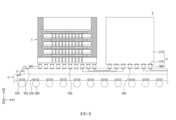
根據本揭露實施例,一種半導體封裝可包括:封裝基板;中介層,位於封裝基板上;第一半導體晶片,位於中介層上;以及封裝,相鄰於第一半導體晶片設置。所述封裝可包括:多個第二半導體晶片,在垂直方向上進行堆疊;以及第一連接端子、第二連接端子、第三連接端子及第四連接端子,將第二半導體晶片彼此連接。所述第二半導體晶片中的每一者可包括:半導體基板;多個穿透電極,被設置成穿透半導體基板;內連線層,設置於半導體基板的表面上;以及訊號接墊群組、電源接墊群組、接地接墊群組及虛設接墊群組,設置於內連線層上。訊號接墊群組、電源接墊群組、接地接墊群組及虛設接墊群組可分別包括訊號接墊、電源接墊、接地接墊及虛設接墊。第一連接端子可以一對多的方式與電源接墊接觸,且第二連接端子可以一對多的方式與接地接墊接觸。第三連接端子可以一對多的方式與虛設接墊接觸,且第四連接端子中的每一者可以一對一的方式與訊號接墊中的對應一者接觸。第一連接端子至第三連接端子中的一者的縱橫比可小於第四連接端子的縱橫比。According to an embodiment of the present disclosure, a semiconductor package may include: a package substrate; an interposer located on the package substrate; a first semiconductor chip located on the interposer; and a package disposed adjacent to the first semiconductor chip. The package may include: a plurality of second semiconductor chips stacked in a vertical direction; and first, second, third and fourth connection terminals connecting the second semiconductor chips to each other. Each of the second semiconductor chips may include: a semiconductor substrate; a plurality of penetrating electrodes disposed to penetrate the semiconductor substrate; an interconnection layer disposed on a surface of the semiconductor substrate; and a signal pad group , the power pad group, the ground pad group and the dummy pad group are arranged on the internal connection layer. The signal pad group, the power pad group, the ground pad group and the dummy pad group may respectively include signal pads, power pads, ground pads and dummy pads. The first connection terminals can be in contact with the power pads in a one-to-many manner, and the second connection terminals can be in contact with the ground pads in a one-to-many manner. The third connection terminals can be in contact with the dummy pads in a one-to-many manner, and each of the fourth connection terminals can be in contact with a corresponding one of the signal pads in a one-to-one manner. An aspect ratio of one of the first to third connection terminals may be smaller than that of the fourth connection terminal.
現在將參考附圖更全面地闡述本揭露的實例性實施例,在附圖中示出實例性實施例。Example embodiments of the present disclosure will now be described more fully with reference to the accompanying drawings, in which example embodiments are shown.
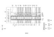
圖1是示意性地示出根據本揭露實施例的半導體封裝1的剖視圖。FIG. 1 is a cross-sectional view schematically showing a
參照圖1,可提供封裝1,且封裝1可被稱為半導體晶片堆疊ST。半導體晶片堆疊ST可包括多個第一半導體晶片100及100t、第二半導體晶片200、模製構件MD及黏合層AD,黏合層AD設置於第一半導體晶片100與第一半導體晶片100t之間以及第一半導體晶片100與第二半導體晶片200之間。Referring to FIG. 1 , a
第一半導體晶片100與第一半導體晶片100t可在垂直方向上堆疊於第二半導體晶片200的頂表面上。在實施例中,第一半導體晶片100及第一半導體晶片100t中的至少一者可為記憶體晶片。記憶體晶片可為動態隨機存取記憶體(dynamic random access memory,DRAM)晶片及靜態隨機存取記憶體(static random access memory,SRAM)晶片中的一者。The first semiconductor wafer 100 and the
第二半導體晶片200可被稱為基礎晶片或緩衝器晶片。在實施例中,第二半導體晶片200可為邏輯晶片。邏輯晶片可為圖形處理單元(graphics processing unit,GPU)晶片及系統晶片(system on chip,SOC)晶片中的一者。The
模製構件MD可覆蓋第一半導體晶片100的側表面及第一半導體晶片100t的側表面、第二半導體晶片200的頂表面以及黏合層AD的側表面。在實施例中,模製構件MD可由環氧化合物形成或者可包含所述環氧化合物。第一半導體晶片100中的每一者可包括第一半導體基板110、內連線層120、第一保護層190(例如,參見圖2)、第二保護層150及第一穿透電極140。The molding member MD may cover side surfaces of the first semiconductor wafer 100 and side surfaces of the first semiconductor wafer 100t, a top surface of the second semiconductor wafer 200, and side surfaces of the adhesive layer AD. In an embodiment, the molding member MD may be formed of epoxy compound or may include the epoxy compound. Each of the
在實施例中,第一半導體基板110可由矽形成或者可包含矽。第一半導體基板110可包括彼此相對的第一表面110a與第二表面110b。第一表面110a上可設置有內連線層120。內連線層120的底表面上可設置有第一保護層190。第一保護層190可由絕緣材料形成或者可包含所述絕緣材料(例如,氮化矽層)。In an embodiment, the
第一保護層190上可設置有第一下部接墊群組160。第一下部接墊群組160可由導電材料(例如,銅)形成或者可包含所述導電材料。第一下部接墊群組160可包括第一下部電壓接墊群組161、第一下部虛設接墊群組162及第一下部訊號接墊群組163。第一下部虛設接墊群組162可被稱為下部熱量傳遞接墊群組162。A first
第二表面110b上可設置有第二保護層150。第二保護層150上可設置有第一上部接墊群組170。第一上部接墊群組170可由導電材料(例如,銅)形成或者可包含所述導電材料。第一上部接墊群組170可包括第一上部電壓接墊群組171、第一上部虛設接墊群組172及第一上部訊號接墊群組173。第一上部虛設接墊群組172可被稱為上部熱量傳遞接墊群組172。A second
第一穿透電極140可被設置成穿透第一半導體基板110。第一穿透電極140可將第一下部電壓接墊群組161及第一下部訊號接墊群組163分別電性連接至第一上部電壓接墊群組171及第一上部訊號接墊群組173。The
第一下部接墊群組160上可設置有連接端子CN。舉例而言,連接端子CN可設置於第一半導體晶片100中位於上部的一者的第一下部接墊群組160與第一半導體晶片100中位於下部的一者的第一上部接墊群組170之間。Connection terminals CN may be disposed on the first
連接端子CN中的每一者可由導電材料(例如,焊接材料)中的至少一者形成或者可包含所述至少一者。在下文中將更詳細地對連接端子CN進行闡述。Each of the connection terminals CN may be formed of or include at least one of conductive materials (eg, solder material). The connection terminal CN will be explained in more detail below.
作為第一半導體晶片100與第一半導體晶片100t中的最上一者的第一半導體晶片100t的第一半導體基板110可較其他的第一半導體晶片100的第一半導體基板厚。第一半導體晶片100t可不包括第一上部接墊群組170及第一穿透電極140。在實施例中,第一半導體晶片100t可包括第一穿透電極140,但不包括第一上部接墊群組170。The
第二半導體晶片200可包括第二半導體基板210、第二內連線層220、第二穿透電極240、第三保護層(未示出)、第四保護層250、第二上部接墊群組270及下部接墊260。The
第二上部接墊群組270可包括第二上部電壓接墊群組271、第二上部虛設接墊群組272及第二上部訊號接墊群組273。下部接墊260可包括訊號接墊及電壓接墊。下部接墊260上可分別設置有封裝連接端子280。The second
黏合層AD可被設置成包圍連接端子CN且防止在連接端子CN之間產生意料之外的電流。在實施例中,黏合層AD可為非導電膜。The adhesive layer AD may be provided to surround the connection terminals CN and prevent unexpected current from being generated between the connection terminals CN. In an embodiment, the adhesive layer AD may be a non-conductive film.
第一半導體晶片100中的相鄰者之間的區以及彼此相鄰的第一半導體晶片100與第二半導體晶片200之間的區中的每一者均可被稱為連接區CR。Each of a region between adjacent ones of the
在實施例中,相鄰的第一半導體晶片100中位於上部的一者的第一下部接墊群組160、相鄰的第一半導體晶片100中位於下部的一者的第一上部接墊群組170以及連接端子CN可放置於第一半導體晶片100中的相鄰者之間的連接區CR中。在下文中將更詳細地對連接區CR進行闡述。In an embodiment, the first
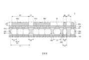
圖2是示出圖1所示連接區CR及其鄰近區的放大剖視圖。圖3是示出圖2所示部分「A」的放大剖視圖。FIG. 2 is an enlarged cross-sectional view showing the connection region CR shown in FIG. 1 and its vicinity. Fig. 3 is an enlarged cross-sectional view showing a portion "A" shown in Fig. 2 .
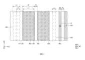
圖4是示例性地示出金屬層與連接端子的排列方式的平面圖。FIG. 4 is a plan view exemplarily showing the arrangement of metal layers and connection terminals.
參照圖1至圖3,第一下部電壓接墊群組161可包括第一下部電源接墊群組161a及第一下部接地接墊群組161b。第一下部電源接墊群組161a可包括彼此相鄰設置的多個第一下部電源接墊61a。第一下部接地接墊群組161b可包括彼此相鄰設置的多個第一下部接地接墊61b。第一下部虛設接墊群組162可包括彼此相鄰設置的多個第一下部虛設接墊62。第一下部訊號接墊群組163可包括彼此相鄰設置的多個第一下部訊號接墊63。1 to 3, the first lower
第一上部電壓接墊群組171可包括第一上部電源接墊群組171a及第一上部接地接墊群組171b。第一上部電源接墊群組171a可包括彼此相鄰設置的多個第一上部電源接墊71a。第一上部接地接墊群組171b可包括彼此相鄰設置的多個第一上部接地接墊71b。第一上部虛設接墊群組172可包括彼此相鄰設置的多個第一上部虛設接墊72。第一上部訊號接墊群組173可包括彼此相鄰設置的多個第一上部訊號接墊73。The first upper
第一穿透電極140可包括電源穿透電極141、接地穿透電極142及訊號穿透電極143。在第一半導體晶片100中的每一者中,電源穿透電極141可連接至第一上部電源接墊71a,且可經由內連線層120連接至第一下部電源接墊61a。在第一半導體晶片100中的每一者中,接地穿透電極142可連接至第一上部接地接墊71b,且可經由內連線層120連接至第一下部接地接墊61b。在第一半導體晶片100中的每一者中,訊號穿透電極143可連接至第一上部訊號接墊73,且可經由內連線層120連接至第一下部訊號接墊63。The first
內連線層120可包括絕緣層121以及金屬層M1、金屬層M2及金屬層M3。金屬層M1、金屬層M2及金屬層M3可設置於絕緣層121中。與圖式中所示的不同,絕緣層121可由多個絕緣層構成。在實施例中,絕緣層121可包括氧化矽層。The
金屬層M1、金屬層M2及金屬層M3可在與第一半導體基板110的第一表面110a平行的第一方向D1或第二方向D2上延伸。金屬層M1、金屬層M2及金屬層M3可包括依序地堆疊於第一表面110a上的第一金屬層M1、第二金屬層M2及第三金屬層M3。儘管金屬層被示出為包括三個金屬層(例如,M1、M2及M3),然而本揭露並不限於所示出的金屬層的數目。The metal layer M1 , the metal layer M2 and the metal layer M3 may extend in a first direction D1 or a second direction D2 parallel to the
第一金屬層M1可與第一穿透電極140接觸。第三金屬層M3可對應於最相鄰於第一下部電源接墊群組161a、第一下部接地接墊群組161b及第一下部訊號接墊群組163的金屬層。第一金屬層M1至第三金屬層M3中的相鄰者可經由夾置於其間的通孔而彼此連接。The first metal layer M1 may make contact with the
第三金屬層M3的厚度可大於第一金屬層M1的厚度及第二金屬層M2的厚度。在實施例中,第三金屬層M3的厚度T1可介於2微米至3微米的範圍內。The thickness of the third metal layer M3 may be greater than the thickness of the first metal layer M1 and the thickness of the second metal layer M2. In an embodiment, the thickness T1 of the third metal layer M3 may range from 2 micrometers to 3 micrometers.
在實施例中,第一金屬層M1及第二金屬層M2可由銅形成或者可包含銅。第三金屬層M3可由例如鋁形成或者可包含例如鋁。In an embodiment, the first metal layer M1 and the second metal layer M2 may be formed of copper or may include copper. The third metal layer M3 may be formed of, for example, aluminum or may contain, for example, aluminum.
參照圖4,第三金屬層M3可包括電源線M3a、接地線M3b及訊號線M3c。Referring to FIG. 4, the third metal layer M3 may include a power line M3a, a ground line M3b, and a signal line M3c.
電源線M3a及接地線M3b在第一方向D1上可具有第一寬度W1,而訊號線M3c在第一方向D1上可具有第二寬度W2。在實施例中,第一寬度W1可介於80微米至120微米的範圍內。在實施例中,第二寬度W2可介於8微米至12微米的範圍內。第一寬度W1可較第二寬度W2大五倍。The power line M3a and the ground line M3b may have a first width W1 in the first direction D1, and the signal line M3c may have a second width W2 in the first direction D1. In an embodiment, the first width W1 may be in a range of 80 microns to 120 microns. In an embodiment, the second width W2 may be in a range of 8 microns to 12 microns. The first width W1 may be five times larger than the second width W2.
電源線M3a中的每一者及接地線M3b中的每一者可在平行於第一半導體基板110的第一表面110a且不平行於第一方向D1的第二方向D2上延伸。Each of the power lines M3a and each of the ground lines M3b may extend in a second direction D2 parallel to the
如圖2中所示,第一下部電源接墊群組161a可與電源線M3a接觸。即,第一下部電源接墊61a可以多對一的方式與電源線M3a接觸。第一下部接地接墊群組161b可與接地線M3b接觸。換言之,第一下部接地接墊61b可以多對一的方式與接地線M3b接觸。第一下部訊號接墊63中的每一者可以一對一的方式與訊號線M3c中對應一者接觸。As shown in FIG. 2, the first lower
第一下部虛設接墊群組162可與第三金屬層M3間隔開。第一下部虛設接墊62可不與第三金屬層M3接觸。The first lower
連接端子CN可包括第一連接端子CN1、第二連接端子CN2、第三連接端子CN3及第四連接端子CN4。第一連接端子CN1可設置於第一半導體晶片100中位於上部的一者的第一下部電源接墊群組161a與第一半導體晶片100中位於下部的一者的第一上部電源接墊群組171a之間。第二連接端子CN2可設置於第一半導體晶片100中位於上部的一者的第一下部接地接墊群組161b與第一半導體晶片100中位於下部的一者的第一上部接地接墊群組171b之間。第三連接端子CN3可設置於第一半導體晶片100中位於上部的一者的第一下部虛設接墊群組162與第一半導體晶片100中位於下部的一者的第一上部虛設接墊群組172之間。第四連接端子CN4可設置於第一下部訊號接墊63中的每一者與第一上部訊號接墊73中的每一者之間。第一連接端子CN1可以一對多的方式連接至第一半導體晶片100中位於上部的一者的第一下部電源接墊61a。另外,第一連接端子CN1可以一對多的方式連接至第一半導體晶片100中位於下部的一者的第一上部電源接墊71a。The connection terminals CN may include a first connection terminal CN1, a second connection terminal CN2, a third connection terminal CN3, and a fourth connection terminal CN4. The first connection terminal CN1 may be disposed on the first lower
第二連接端子CN2可以一對多的方式連接至第一半導體晶片100中位於上部的一者的第一下部接地接墊61b。此外,第二連接端子CN2可以一對多的方式連接至第一半導體晶片100中位於下部的一者的第一上部接地接墊71b。The second connection terminal CN2 may be connected to the first
第三連接端子CN3可以一對多的方式連接至第一半導體晶片100中位於上部的一者的第一下部虛設接墊62。此外,第三連接端子CN3可以一對多的方式連接至第一半導體晶片100中位於下部的一者的第一上部虛設接墊72。The third connection terminal CN3 may be connected to the first
第一下部虛設接墊62中的每一者的一部分可與第三連接端子CN3接觸,且其餘部分可與絕緣層121及第一保護層190接觸。A portion of each of the first
第四連接端子CN4可以一對一的方式連接至第一半導體晶片100中位於上部的一者的第一下部訊號接墊63中的每一者。此外,第四連接端子CN4可以一對一的方式連接至第一半導體晶片100中位於下部的一者的上部訊號接墊73。The fourth connection terminal CN4 may be connected to each of the first
第一連接端子CN1至第三連接端子CN3中的每一者可具有由合併的凸塊構成的結構。Each of the first to third connection terminals CN1 to CN3 may have a structure composed of merged bumps.
參照圖3及圖4,電源線M3a及接地線M3b可在第二方向D2上延伸,且可在第一方向D1上彼此間隔開第一分隔距離P1。在實施例中,電源線M3a與接地線M3b可交替地進行排列。在實施例中,第一分隔距離P1可為約20微米。第一分隔距離P1可小於第一寬度W1。3 and 4, the power line M3a and the ground line M3b may extend in the second direction D2, and may be spaced apart from each other by a first separation distance P1 in the first direction D1. In an embodiment, the power lines M3a and the ground lines M3b may be arranged alternately. In an embodiment, the first separation distance P1 may be about 20 microns. The first separation distance P1 may be smaller than the first width W1.
訊號線M3c可在第二方向D2上延伸,且可在第一方向D1上彼此間隔開第二分隔距離P2。在實施例中,第二分隔距離P2可為約20微米。第二分隔距離P2可大於第二寬度W2。The signal lines M3c may extend in the second direction D2, and may be spaced apart from each other by a second separation distance P2 in the first direction D1. In an embodiment, the second separation distance P2 may be about 20 microns. The second separation distance P2 may be greater than the second width W2.
第一連接端子CN1可在垂直方向上與電源線M3a交疊。第二連接端子CN2可在垂直方向上與接地線M3b交疊。第四連接端子CN4可在垂直方向上與訊號線M3c交疊。The first connection terminal CN1 may overlap the power line M3a in a vertical direction. The second connection terminal CN2 may overlap the ground line M3b in a vertical direction. The fourth connection terminal CN4 may overlap the signal line M3c in the vertical direction.
第三連接端子CN3可被設置成在垂直方向上與上面並未設置電源線M3a、接地線M3b及訊號線M3c的區交疊。作為實例,第三連接端子CN3可設置於電源線M3a與接地線M3b之間,或者可被設置成在垂直方向上與位於電源線M3a或接地線M3b與訊號線M3c之間的區交疊。The third connection terminal CN3 may be disposed to overlap a region on which the power line M3a, the ground line M3b, and the signal line M3c are not disposed in the vertical direction. As an example, the third connection terminal CN3 may be disposed between the power line M3a and the ground line M3b, or may be disposed to overlap a region between the power line M3a or the ground line M3b and the signal line M3c in a vertical direction.
第一連接端子CN1及第二連接端子CN2在第一方向D1上可具有寬度L1。在其中第一連接端子CN1及第二連接端子CN2在第二方向D2上延伸的情形中,第一方向D1上的寬度L1可為最小寬度。在其中第三連接端子CN3在第二方向D2上延伸的情形中,第一方向D1上的寬度L2可為最小寬度。第一連接端子CN1至第三連接端子CN3的最小寬度可大於第四連接端子CN4的最大寬度。當在同一水平處進行量測時,第一連接端子CN1至第三連接端子CN3的寬度L1及寬度L2可大於第四連接端子CN4的寬度L3。第一連接端子CN1至第三連接端子CN3中的每一者的縱橫比可小於第四連接端子CN4的縱橫比。在本說明書中,縱橫比可意指藉由將物體的厚度或高度(即,在第三方向D3上的長度)除以物體在第一方向D1或第二方向D2上的寬度而獲得的值。第一連接端子CN1至第三連接端子CN3的最小寬度L1或最小寬度L2可實質上等於第一凸塊BP1的最大直徑。第四連接端子CN4可為第二凸塊BP2。第一凸塊BP1的直徑L4可大於第二凸塊BP2的最大直徑。The first connection terminal CN1 and the second connection terminal CN2 may have a width L1 in the first direction D1. In the case where the first connection terminal CN1 and the second connection terminal CN2 extend in the second direction D2, the width L1 in the first direction D1 may be the minimum width. In the case where the third connection terminal CN3 extends in the second direction D2, the width L2 in the first direction D1 may be the minimum width. The minimum width of the first to third connection terminals CN1 to CN3 may be greater than the maximum width of the fourth connection terminal CN4. When measured at the same level, the width L1 and the width L2 of the first connecting terminal CN1 to the third connecting terminal CN3 may be larger than the width L3 of the fourth connecting terminal CN4. An aspect ratio of each of the first to third connection terminals CN1 to CN3 may be smaller than that of the fourth connection terminal CN4. In this specification, the aspect ratio may mean a value obtained by dividing the thickness or height (ie, the length in the third direction D3) of the object by the width of the object in the first direction D1 or the second direction D2 . The minimum width L1 or the minimum width L2 of the first to third connection terminals CN1 to CN3 may be substantially equal to the maximum diameter of the first bump BP1. The fourth connection terminal CN4 may be the second bump BP2. The diameter L4 of the first bump BP1 may be larger than the maximum diameter of the second bump BP2.
在第一下部電源接墊群組161a中,第一下部電源接墊61a之間的分隔距離K2可小於第一下部電源接墊61a中的每一者的直徑。此外,第一上部電源接墊群組171a、第一下部接地接墊群組161b、第一上部接地接墊群組171b、第一下部虛設接墊群組162及第一上部虛設接墊群組172亦可被配置成具有與第一下部電源接墊群組161a中的距離-直徑關係相同的距離-直徑關係;即,在每一組中,接墊之間的分隔距離可小於每一接墊的直徑。In the first lower
因此,當在第一下部電源接墊61a、第一下部接地接墊61b及第一下部虛設接墊62上對第一凸塊BP1進行迴焊時,或者當第一半導體晶片100彼此貼合時,第一凸塊BP1中的相鄰者可彼此接觸且可輕易地彼此結合。Therefore, when the first bump BP1 is reflowed on the first
第一下部電源接墊群組161a可與相鄰於第一下部電源接墊群組161a的第一下部接地接墊群組161b間隔開分隔距離K3,且此處,分隔距離K3可等於或大於第一下部電源接墊61a的直徑K1。因此,在其中第一凸塊BP1中的相鄰者被合併以形成第一連接端子CN1及第二連接端子CN2的情形中,第一連接端子CN1與第二連接端子CN2無法彼此接觸。The first lower
其他的接墊群組可被配置成具有相同的關係;舉例而言,不同的接墊群組之間的分隔距離可等於或大於每一接墊的直徑。第一下部訊號接墊63的直徑K4可小於第一下部電源接墊61a的直徑K1。第一下部訊號接墊63的直徑K4可小於第一下部接地接墊61b的直徑及第一下部虛設接墊62的直徑。另外,第一下部訊號接墊63的直徑K4可小於或等於第一下部訊號接墊63至與其相鄰的另一第一下部訊號接墊63的距離。因此,可防止第四連接端子CN4中的相鄰者在形成第四連接端子CN4的製程中彼此接觸。Other groups of pads can be configured to have the same relationship; for example, the separation distance between different groups of pads can be equal to or greater than the diameter of each pad. The diameter K4 of the first
根據本揭露實施例,第一下部電源接墊群組及第一下部接地接墊群組可分別連接至面積大且厚度大的電源線及接地線。第一下部電源接墊群組中的第一下部電源接墊可以多對一的方式耦合至第一連接端子,且第一下部接地接墊群組中的第一下部接地接墊可以多對一的方式耦合至第二連接端子。此外,第一下部虛設接墊群組可設置於其中並未設置電源線及接地線的區上,且第一下部虛設接墊可以多對一的方式耦合至第三連接端子。即,由於第一連接端子及第二連接端子被設置成具有增大的面積,因此可有效地實行自第一半導體晶片中位於下部的一者朝向第一半導體晶片中位於上部的一者的熱量傳遞過程(heat transfer process)。另外,由於第三連接端子被設置於未使用的區域上,因此可更有效地實行熱量傳遞過程。因此,可提高半導體晶片堆疊中的向上熱量傳遞過程的效率,或者降低半導體封裝在垂直方向上的熱阻。According to an embodiment of the present disclosure, the first lower power pad group and the first lower ground pad group can be respectively connected to the power line and the ground line with a large area and a large thickness. The first lower power pads in the first lower power pad group can be coupled to the first connection terminal in a many-to-one manner, and the first lower ground pads in the first lower ground pad group Can be coupled to the second connection terminal in a many-to-one manner. In addition, the first lower dummy pad group may be disposed on the region where no power line and ground line are disposed, and the first lower dummy pad may be coupled to the third connection terminal in a many-to-one manner. That is, since the first connection terminal and the second connection terminal are provided to have an increased area, heat transfer from the lower one of the first semiconductor wafers toward the upper one of the first semiconductor wafers can be effectively performed. Heat transfer process. In addition, since the third connection terminal is disposed on the unused area, the heat transfer process can be performed more efficiently. Therefore, the efficiency of the upward heat transfer process in the semiconductor wafer stack can be improved, or the thermal resistance of the semiconductor package in the vertical direction can be reduced.
圖5是示意性地示出連接端子的排列方式的平面圖。FIG. 5 is a plan view schematically showing an arrangement of connection terminals.
參照圖5,第一半導體晶片100的底表面上可設置有第一連接端子區CN1R或第二連接端子區CN2R。在實施例中,第一半導體晶片的中心部分上可設置有第四連接端子區CN4R。上面並未設置第一連接端子區CN1R或第二連接端子區CN2R及第四連接端子區CN4R的區可充當上面設置有第三連接端子CN3的第三連接端子區CN3R。在實施例中,第三連接端子區CN3R可佔平面面積的20%至50%。Referring to FIG. 5 , a first connection terminal region CN1R or a second connection terminal region CN2R may be disposed on the bottom surface of the
圖6是示出根據本揭露實施例的連接區及其鄰近區的放大剖視圖。除以下將闡述的特徵以外,根據本實施例的封裝可具有與參照圖1至圖5所闡述的特徵實質上相同的特徵,且因此,可不再對其重複說明予以贅述。FIG. 6 is an enlarged cross-sectional view illustrating a connection region and its adjacent regions according to an embodiment of the present disclosure. The package according to the present embodiment may have substantially the same features as those explained with reference to FIGS. 1 to 5 except for features to be described below, and therefore, repeated descriptions thereof will not be repeated.
第一下部電源接墊群組161a中彼此相鄰的第一下部電壓接墊61之間的分隔距離K2可等於或大於第一下部電壓接墊61中的每一者的直徑K1。第一下部電源接墊群組161a與第一下部接地接墊群組161b之間的分隔距離K3可大於第一下部電壓接墊61中的相鄰者之間的分隔距離K2。在此種情形中,構成第一連接端子CN1的每一第一凸塊BP1的直徑可較第一下部電壓接墊61的直徑大1.5倍。A separation distance K2 between first lower voltage pads 61 adjacent to each other in the first lower
圖7是示出根據本揭露實施例的連接區及其鄰近區的放大剖視圖。除以下將闡述的特徵以外,根據本實施例的封裝可具有與參照圖1至圖5所闡述的特徵實質上相同的特徵,且因此,可不再對其重複說明予以贅述。FIG. 7 is an enlarged cross-sectional view illustrating a connection region and its adjacent regions according to an embodiment of the present disclosure. The package according to the present embodiment may have substantially the same features as those explained with reference to FIGS. 1 to 5 except for features to be described below, and therefore, repeated descriptions thereof will not be repeated.
參照圖7,第一連接端子CN1至第三連接端子CN3中的每一者可包括金屬結構MS。在實施例中,金屬結構MS可由銅形成或者可包含銅。當在剖視圖中觀察時,金屬結構MS可具有矩形形狀。金屬結構MS中的一些金屬結構MS可在垂直方向上與電源線M3a及接地線M3b交疊。第四連接端子CN4可包括凸塊。Referring to FIG. 7 , each of the first to third connection terminals CN1 to CN3 may include a metal structure MS. In an embodiment, the metal structure MS may be formed of copper or may include copper. The metal structure MS may have a rectangular shape when viewed in a cross-sectional view. Some of the metal structures MS may overlap the power line M3a and the ground line M3b in the vertical direction. The fourth connection terminal CN4 may include a bump.
圖8是示出根據本揭露實施例的連接區及其鄰近區的放大剖視圖。除以下將闡述的特徵以外,根據本實施例的封裝可具有與參照圖1至圖5所闡述的特徵實質上相同的特徵,且因此,可不再對其重複說明予以贅述。FIG. 8 is an enlarged cross-sectional view illustrating a connection region and its adjacent regions according to an embodiment of the present disclosure. The package according to the present embodiment may have substantially the same features as those explained with reference to FIGS. 1 to 5 except for features to be described below, and therefore, repeated descriptions thereof will not be repeated.
參考圖8,第一下部電源接墊61a、第一下部接地接墊61b及第一下部虛設接墊62中的每一者可被設置成包括多個通孔。第一上部電源接墊71a可被設置成以一對多的方式與多個電源穿透電極141接觸,而第一上部接地接墊71b可被設置成以一對多的方式與多個接地穿透電極142接觸。第一上部虛設接墊72可具有與第一下部虛設接墊62對應的大小。Referring to FIG. 8, each of the first
金屬結構MS可設置於第一半導體晶片100中位於上部的一者的第一下部電源接墊61a、第一下部接地接墊61b及第一下部虛設接墊62與第一半導體晶片100中位於下部的一者的第一上部電源接墊71a、第一上部接地接墊71b及第一上部虛設接墊72的每一對應的對之間。The metal structure MS can be disposed on the first
圖9是示出根據本揭露實施例的連接區及其鄰近區的放大剖視圖。除以下將闡述的特徵以外,根據本實施例的封裝可具有與參照圖1至圖5所闡述的特徵實質上相同的特徵,且因此,可不再對其重複說明予以贅述。FIG. 9 is an enlarged cross-sectional view illustrating a connection region and its adjacent regions according to an embodiment of the present disclosure. The package according to the present embodiment may have substantially the same features as those explained with reference to FIGS. 1 to 5 except for features to be described below, and therefore, repeated descriptions thereof will not be repeated.
參照圖9,第一半導體晶片100中位於上部的一者的第一下部電源接墊61a可與第一半導體晶片100中位於下部的一者的第一上部電源接墊71a接觸。第一半導體晶片100中位於上部的一者的第一下部接地接墊61b可與第一半導體晶片100中位於下部的一者的第一上部接地接墊71b接觸。第一半導體晶片100中位於上部的一者的第一下部虛設接墊62可與第一半導體晶片100中位於下部的一者的第一上部虛設接墊72接觸。第一半導體晶片100中位於上部的一者的第一下部訊號接墊63可與第一半導體晶片100中位於下部的一者的第一上部訊號接墊73接觸。Referring to FIG. 9 , the first
圖10是示出根據本揭露實施例的半導體封裝5的平面圖。圖11是沿圖10所示線I-I'截取的剖視圖。FIG. 10 is a plan view showing a semiconductor package 5 according to an embodiment of the present disclosure. FIG. 11 is a cross-sectional view taken along line II' shown in FIG. 10 .
參照圖10及圖11,半導體封裝5可包括封裝基板4、中介層3、半導體晶片堆疊1及第三半導體晶片2。在實施例中,可提供多個半導體晶片堆疊1。舉例而言,第三半導體晶片2的兩個相對側中的每一側上可設置有兩個半導體晶片堆疊1;即,第三半導體晶片2周圍總共可設置有四個半導體晶片堆疊1。Referring to FIGS. 10 and 11 , the semiconductor package 5 may include a
在實施例中,封裝基板4可為印刷電路板(printed circuit board)。中介層3可為矽中介層或重佈線中介層。In an embodiment, the
第三半導體晶片2可為邏輯晶片。第三半導體晶片2可包括第三基板310。第三基板310可具有面向中介層3且充當設置有電路層的有效表面的表面。所述有效表面上可設置有下部接墊370。下部接墊370上可設置有連接端子380。The
中介層3可包括第一接墊430及第二接墊440。封裝連接端子280可連接至第一接墊430。連接端子380可連接至第二接墊440。第三半導體晶片2與半導體晶片堆疊1可經由中介層3彼此電性連接。The
中介層3可包括第三接墊420,且可經由第三接墊420及連接元件(例如,接合配線或TSV)連接至封裝基板4。封裝基板4可包括上部接墊520及下部接墊530。下部接墊530上可設置有外部連接端子580。封裝基板4可經由外部連接端子580電性連接至外部板(例如,母板(motherboard))。The
根據本揭露實施例,堆疊的半導體晶片之間可設置有以一對多的方式分別連接至電壓接墊、接地接墊及虛設接墊的第一連接端子、第二連接端子及第三連接端子。第一連接端子及第二連接端子可連接至放置於第一連接端子及第二連接端子上的半導體晶片的厚的金屬層。因此,第一連接端子及第二連接端子可用於在向上方向上有效地排出自下伏的半導體晶片產生的熱量。此外,由於第三連接端子的存在,可更有效地實行散熱過程。因此,可降低半導體封裝在垂直方向上的熱阻。According to an embodiment of the present disclosure, a first connection terminal, a second connection terminal and a third connection terminal respectively connected to voltage pads, ground pads and dummy pads in a one-to-many manner may be provided between the stacked semiconductor chips. . The first connection terminal and the second connection terminal can be connected to a thick metal layer of the semiconductor wafer placed on the first connection terminal and the second connection terminal. Therefore, the first connection terminal and the second connection terminal can be used to efficiently dissipate heat generated from the underlying semiconductor wafer in the upward direction. In addition, due to the existence of the third connection terminal, the heat dissipation process can be performed more effectively. Therefore, the thermal resistance of the semiconductor package in the vertical direction can be reduced.
按照本領域中的慣例,可在施行一或多個所闡述功能的區塊角度闡述且示出實施例。該些區塊在本文中可被稱為單元或模組或類似區塊,是由類比電路及/或數位電路(例如邏輯閘、積體電路、微處理器、微控制器、記憶體電路、被動電子組件、主動電子組件、光學組件、硬連線電路及類似電路)在實體上實施且可視需要由韌體及/或軟體驅動。舉例而言,電路可體現於一或多個半導體晶片中或基板支撐件(例如印刷電路板及類似組件)上。構成區塊的電路可由專用硬體實施,或由處理器(例如,一或多個經程式化微處理器及相關聯電路系統)實施,或由實行區塊的一些功能的專用硬體與實行區塊的其他功能的處理器的組合實施。可在不背離本揭露的範圍的條件下將實施例的每一區塊在實體上分隔成二或更多個相互作用且離散的區塊。同樣,可在不背離本揭露的範圍的條件下將實施例的區塊在實體上組合成更複雜的區塊。實施例的態樣可經由儲存於非暫時性儲存媒體內且由處理器執行的指令來達成。Embodiments may be described and shown in terms of blocks that perform one or more described functions, as is customary in the art. These blocks may be referred to herein as units or modules or similar blocks, which are composed of analog circuits and/or digital circuits (such as logic gates, integrated circuits, microprocessors, microcontrollers, memory circuits, Passive electronic components, active electronic components, optical components, hardwired circuits, and the like) are physically implemented and optionally driven by firmware and/or software. For example, circuits may be embodied in one or more semiconductor dies or on substrate supports such as printed circuit boards and similar components. The circuits making up the blocks may be implemented by dedicated hardware, by a processor (e.g., one or more programmed microprocessors and associated circuitry), or by dedicated hardware that performs some of the functions of the blocks. A combination of processors implements the other functions of the block. Each block of an embodiment may be physically separated into two or more interacting and discrete blocks without departing from the scope of the present disclosure. Also, blocks of the embodiments may be physically combined into more complex blocks without departing from the scope of the present disclosure. Aspects of the embodiments may be implemented by instructions stored in a non-transitory storage medium and executed by a processor.
儘管已具體示出並闡述了本揭露的實例性實施例,然而此項技術中具有通常知識者應理解,在不背離隨附申請專利範圍的精神及範圍的條件下,可對其作出各種形式及細節上的改變。While exemplary embodiments of the present disclosure have been shown and described in detail, it will be understood by those of ordinary skill in the art that various forms may be made therein without departing from the spirit and scope of the appended claims. and changes in details.
1:半導體晶片堆疊/半導體封裝/封裝 2:第三半導體晶片 3:中介層 4:封裝基板 5:半導體封裝 61a:第一下部電源接墊 61b:第一下部接地接墊 62:第一下部虛設接墊 63:第一下部訊號接墊 71a:第一上部電源接墊 71b:第一上部接地接墊 72:第一上部虛設接墊 73:第一上部訊號接墊/上部訊號接墊 100、100t:第一半導體晶片 110:第一半導體基板 110a:第一表面 110b:第二表面 120:內連線層 121:絕緣層 140:第一穿透電極 141:電源穿透電極 142:接地穿透電極 143:訊號穿透電極 150:第二保護層 160:第一下部接墊群組 161:第一下部電壓接墊群組 161a:第一下部電源接墊群組 161b:第一下部接地接墊群組 162:第一下部虛設接墊群組/下部熱量傳遞接墊群組 163:第一下部訊號接墊群組 170:第一上部接墊群組 171:第一上部電壓接墊群組 171a:第一上部電源接墊群組 171b:第一上部接地接墊群組 172:第一上部虛設接墊群組/上部熱量傳遞接墊群組 173:第一上部訊號接墊群組 190:第一保護層 200:第二半導體晶片 210:第二半導體基板 220:第二內連線層 240:第二穿透電極 250:第四保護層 260:下部接墊 270:第二上部接墊群組 271:第二上部電壓接墊群組 272:第二上部虛設接墊群組 273:第二上部訊號接墊群組 280:封裝連接端子 310:第三基板 370、530:下部接墊 380:連接端子 420:第三接墊 430:第一接墊 440:第二接墊 520:上部接墊 580:外部連接端子 A:部分 AD:黏合層 BP1:第一凸塊 BP2:第二凸塊 CN:連接端子 CN1:第一連接端子 CN1R:第一連接端子區 CN2:第二連接端子 CN2R:第二連接端子區 CN3:第三連接端子 CN3R:第三連接端子區 CN4:第四連接端子 CN4R:第四連接端子區 CR:連接區 D1:第一方向 D2:第二方向 D3:第三方向 I-I':線 K1、K4、L4:直徑 K2、K3:分隔距離 L1、L2:最小寬度/寬度 L3:寬度 M1:第一金屬層/金屬層 M2:第二金屬層/金屬層 M3:第三金屬層/金屬層 M3a:電源線 M3b:接地線 M3c:訊號線 MD:模製構件 MS:金屬結構 P1:第一分隔距離 P2:第二分隔距離 ST:半導體晶片堆疊 T1:厚度 W1:第一寬度 W2:第二寬度1: Semiconductor wafer stacking/semiconductor packaging/packaging 2: The third semiconductor wafer 3: intermediary layer 4: Package substrate 5: Semiconductor packaging 61a: First lower power pad 61b: First lower ground pad 62: First lower dummy pad 63: The first lower signal pad 71a: First upper power pad 71b: First upper ground pad 72: First upper dummy pad 73: The first upper signal pad/upper signal pad 100, 100t: the first semiconductor wafer 110: the first semiconductor substrate 110a: first surface 110b: second surface 120: Inner layer 121: insulation layer 140: The first penetrating electrode 141: Power penetrating electrode 142: Ground penetration electrode 143: Signal penetration electrode 150: second protective layer 160: First lower pad group 161: First lower voltage pad group 161a: First lower power pad group 161b: First lower ground pad group 162: First lower dummy pad group/lower heat transfer pad group 163: The first lower signal pad group 170: First upper pad group 171: First upper voltage pad group 171a: First upper power pad group 171b: First upper ground pad group 172: First upper dummy pad group/upper heat transfer pad group 173: The first upper signal pad group 190: first protective layer 200: second semiconductor wafer 210: second semiconductor substrate 220: Second interconnection layer 240: the second penetrating electrode 250: The fourth protective layer 260: Lower pad 270: Second upper pad group 271: Second upper voltage pad group 272: Second upper dummy pad group 273: The second upper signal pad group 280: package connection terminal 310: the third substrate 370, 530: lower pad 380: Connecting terminal 420: The third pad 430: first pad 440: second pad 520: Upper Pad 580: External connection terminal A: part AD: Adhesive layer BP1: First bump BP2: Second bump CN: Connecting terminal CN1: the first connection terminal CN1R: The first connection terminal area CN2: Second connection terminal CN2R: Second connection terminal area CN3: The third connecting terminal CN3R: The third connection terminal area CN4: The fourth connection terminal CN4R: Fourth connection terminal area CR: connection region D1: the first direction D2: Second direction D3: Third direction I-I': line K1, K4, L4: Diameter K2, K3: separation distance L1, L2: minimum width/width L3: width M1: first metal layer/metal layer M2: second metal layer/metal layer M3: third metal layer/metal layer M3a: Power cord M3b: Ground wire M3c: signal line MD: molded component MS: metal structure P1: first separation distance P2: second separation distance ST: Semiconductor Wafer Stacking T1: Thickness W1: first width W2: second width
圖1是示意性地示出根據本揭露實施例的半導體封裝的剖視圖。 圖2是示出根據本揭露實施例的半導體封裝中的連接區及其鄰近區的放大剖視圖。 圖3是示出圖2所示部分「A」的放大剖視圖。 圖4是示例性地示出圖2所示金屬層與連接端子的排列方式的平面圖。 圖5是示意性地示出設置有連接端子的區的平面圖。 圖6是示出根據本揭露實施例的半導體封裝中的連接區及其鄰近區的放大剖視圖。 圖7是示出根據本揭露實施例的半導體封裝中的連接區及其鄰近區的放大剖視圖。 圖8是示出根據本揭露實施例的半導體封裝中的連接區及其鄰近區的放大剖視圖。 圖9是示出根據本揭露實施例的半導體封裝中的連接區及其鄰近區的放大剖視圖。 圖10是示出根據本揭露實施例的半導體封裝的平面圖。 圖11是沿圖10所示線I-I'截取的剖視圖。FIG. 1 is a cross-sectional view schematically showing a semiconductor package according to an embodiment of the present disclosure. 2 is an enlarged cross-sectional view illustrating a connection region and its vicinity in a semiconductor package according to an embodiment of the present disclosure. Fig. 3 is an enlarged cross-sectional view showing a portion "A" shown in Fig. 2 . FIG. 4 is a plan view exemplarily showing an arrangement of metal layers and connection terminals shown in FIG. 2 . Fig. 5 is a plan view schematically showing a region provided with connection terminals. 6 is an enlarged cross-sectional view illustrating a connection region and its vicinity in a semiconductor package according to an embodiment of the present disclosure. 7 is an enlarged cross-sectional view illustrating a connection region and its vicinity in a semiconductor package according to an embodiment of the present disclosure. 8 is an enlarged cross-sectional view illustrating a connection region and its vicinity in a semiconductor package according to an embodiment of the present disclosure. 9 is an enlarged cross-sectional view illustrating a connection region and its vicinity in a semiconductor package according to an embodiment of the present disclosure. FIG. 10 is a plan view illustrating a semiconductor package according to an embodiment of the present disclosure. FIG. 11 is a cross-sectional view taken along line II' shown in FIG. 10 .
1:半導體晶片堆疊/半導體封裝/封裝1: Semiconductor wafer stacking/semiconductor packaging/packaging
100、100t:第一半導體晶片100, 100t: the first semiconductor wafer
110:第一半導體基板110: the first semiconductor substrate
110a:第一表面110a: first surface
110b:第二表面110b: second surface
120:內連線層120: Inner layer
140:第一穿透電極140: The first penetrating electrode
150:第二保護層150: second protective layer
160:第一下部接墊群組160: First lower pad group
161:第一下部電壓接墊群組161: First lower voltage pad group
162:第一下部虛設接墊群組/下部熱量傳遞接墊群組162: First lower dummy pad group/lower heat transfer pad group
163:第一下部訊號接墊群組163: The first lower signal pad group
170:第一上部接墊群組170: First upper pad group
171:第一上部電壓接墊群組171: First upper voltage pad group
172:第一上部虛設接墊群組/上部熱量傳遞接墊群組172: First upper dummy pad group/upper heat transfer pad group
173:第一上部訊號接墊群組173: The first upper signal pad group
200:第二半導體晶片200: second semiconductor wafer
210:第二半導體基板210: second semiconductor substrate
220:第二內連線層220: Second interconnection layer
240:第二穿透電極240: the second penetrating electrode
250:第四保護層250: The fourth protective layer
260:下部接墊260: Lower pad
270:第二上部接墊群組270: Second upper pad group
271:第二上部電壓接墊群組271: Second upper voltage pad group
272:第二上部虛設接墊群組272: Second upper dummy pad group
273:第二上部訊號接墊群組273: The second upper signal pad group
280:封裝連接端子280: package connection terminal
AD:黏合層AD: Adhesive layer
CN:連接端子CN: Connecting terminal
CR:連接區CR: connection region
D1:第一方向D1: the first direction
D2:第二方向D2: Second direction
D3:第三方向D3: Third direction
MD:模製構件MD: molded component
ST:半導體晶片堆疊ST: Semiconductor Wafer Stacking
Claims (20)
Translated fromChineseApplications Claiming Priority (2)
| Application Number | Priority Date | Filing Date | Title |
|---|---|---|---|
| KR10-2021-0127487 | 2021-09-27 | ||
| KR1020210127487AKR20230044858A (en) | 2021-09-27 | 2021-09-27 | Semiconductor package |
Publications (1)
| Publication Number | Publication Date |
|---|---|
| TW202314988Atrue TW202314988A (en) | 2023-04-01 |
Family
ID=85718880
Family Applications (1)
| Application Number | Title | Priority Date | Filing Date |
|---|---|---|---|
| TW111131663ATW202314988A (en) | 2021-09-27 | 2022-08-23 | Semiconductor package |
Country Status (4)
| Country | Link |
|---|---|
| US (1) | US12142544B2 (en) |
| KR (1) | KR20230044858A (en) |
| CN (1) | CN115881692A (en) |
| TW (1) | TW202314988A (en) |
Cited By (3)
| Publication number | Priority date | Publication date | Assignee | Title |
|---|---|---|---|---|
| US20230096170A1 (en)* | 2021-09-27 | 2023-03-30 | Samsung Electronics Co., Ltd. | Semiconductor package |
| TWI869954B (en)* | 2023-06-01 | 2025-01-11 | 台灣積體電路製造股份有限公司 | Semiconductor package and manufacturing method thereof |
| TWI886745B (en)* | 2024-01-12 | 2025-06-11 | 力晶積成電子製造股份有限公司 | Package architecture with interposer |
Families Citing this family (1)
| Publication number | Priority date | Publication date | Assignee | Title |
|---|---|---|---|---|
| KR20250094137A (en)* | 2023-12-18 | 2025-06-25 | 엘지이노텍 주식회사 | Circuit board and semiconductor package comprising the same |
Family Cites Families (44)
| Publication number | Priority date | Publication date | Assignee | Title |
|---|---|---|---|---|
| US7476976B2 (en) | 2005-02-23 | 2009-01-13 | Texas Instruments Incorporated | Flip chip package with advanced electrical and thermal properties for high current designs |
| KR100753415B1 (en)* | 2006-03-17 | 2007-08-30 | 주식회사 하이닉스반도체 | Stack package |
| TWI303874B (en) | 2006-08-08 | 2008-12-01 | Via Tech Inc | Multi-chip structure |
| US8048794B2 (en) | 2009-08-18 | 2011-11-01 | International Business Machines Corporation | 3D silicon-silicon die stack structure and method for fine pitch interconnection and vertical heat transport |
| US8426959B2 (en)* | 2009-08-19 | 2013-04-23 | Samsung Electronics Co., Ltd. | Semiconductor package and method of manufacturing the same |
| JP5570799B2 (en)* | 2009-12-17 | 2014-08-13 | ピーエスフォー ルクスコ エスエイアールエル | Semiconductor device and manufacturing method thereof |
| JP2013004601A (en)* | 2011-06-14 | 2013-01-07 | Elpida Memory Inc | Semiconductor device |
| US8618647B2 (en) | 2011-08-01 | 2013-12-31 | Tessera, Inc. | Packaged microelectronic elements having blind vias for heat dissipation |
| US8531032B2 (en) | 2011-09-02 | 2013-09-10 | Taiwan Semiconductor Manufacturing Company, Ltd. | Thermally enhanced structure for multi-chip device |
| US9269646B2 (en) | 2011-11-14 | 2016-02-23 | Micron Technology, Inc. | Semiconductor die assemblies with enhanced thermal management and semiconductor devices including same |
| WO2014122882A1 (en)* | 2013-02-05 | 2014-08-14 | パナソニック株式会社 | Semiconductor device |
| US9449947B2 (en) | 2014-07-01 | 2016-09-20 | Taiwan Semiconductor Manufacturing Company, Ltd. | Semiconductor package for thermal dissipation |
| KR102237978B1 (en) | 2014-09-11 | 2021-04-09 | 삼성전자주식회사 | Semiconductor package an And Method Of Fabricating The Same |
| KR102506697B1 (en) | 2016-05-18 | 2023-03-08 | 에스케이하이닉스 주식회사 | Semiconductor package including through mold ball connectors |
| US10573579B2 (en) | 2017-03-08 | 2020-02-25 | Mediatek Inc. | Semiconductor package with improved heat dissipation |
| US10153261B2 (en) | 2017-04-03 | 2018-12-11 | Cisco Technology, Inc. | Cooling system for high power application specific integrated circuit with embedded high bandwidth memory |
| KR102358343B1 (en)* | 2017-08-09 | 2022-02-07 | 삼성전자주식회사 | Semiconductor package |
| JP7001530B2 (en)* | 2018-04-16 | 2022-01-19 | ルネサスエレクトロニクス株式会社 | Semiconductor device |
| US11437294B2 (en) | 2018-08-09 | 2022-09-06 | Intel Corporation | Structures to facilitate heat transfer within package layers to thermal heat sink and motherboard |
| KR102530763B1 (en)* | 2018-09-21 | 2023-05-11 | 삼성전자주식회사 | Method of manufacturing semiconductor packages |
| US10872835B1 (en) | 2019-07-03 | 2020-12-22 | Micron Technology, Inc. | Semiconductor assemblies including vertically integrated circuits and methods of manufacturing the same |
| KR102750896B1 (en)* | 2020-02-11 | 2025-01-08 | 삼성전자주식회사 | Semiconductor packages and method of manufacturing semiconductor packages |
| KR20220101335A (en)* | 2021-01-11 | 2022-07-19 | 삼성전자주식회사 | Semiconductor package including a plurality of semiconductor chips and method for manufacturing the same |
| KR20230044858A (en)* | 2021-09-27 | 2023-04-04 | 삼성전자주식회사 | Semiconductor package |
| KR20230058257A (en)* | 2021-10-22 | 2023-05-03 | 삼성전자주식회사 | Semiconductor device and semiconductor package including the same |
| KR20230063426A (en)* | 2021-11-02 | 2023-05-09 | 삼성전자주식회사 | Semiconductor package and method of manufacturing the same |
| KR20230064406A (en)* | 2021-11-03 | 2023-05-10 | 삼성전자주식회사 | Semiconductor package |
| KR20230073031A (en)* | 2021-11-18 | 2023-05-25 | 삼성전자주식회사 | Three-dimensional integrated circuit structure and method for manufacturing the same |
| KR20230082953A (en)* | 2021-12-02 | 2023-06-09 | 삼성전자주식회사 | Semiconductor device |
| KR20230087821A (en)* | 2021-12-10 | 2023-06-19 | 삼성전자주식회사 | Semiconductor package |
| US20230207414A1 (en)* | 2021-12-28 | 2023-06-29 | Samsung Electronics Co., Ltd. | Semiconductor package having improved heat dissipation characteristics |
| WO2023239188A1 (en)* | 2022-06-08 | 2023-12-14 | 엘지이노텍 주식회사 | Semiconductor package |
| KR20240001869A (en)* | 2022-06-28 | 2024-01-04 | 삼성전자주식회사 | Semiconductor package |
| KR20240005256A (en)* | 2022-07-04 | 2024-01-12 | 삼성전자주식회사 | Semiconductor package and method of manufacturing the same |
| KR20240011485A (en)* | 2022-07-19 | 2024-01-26 | 삼성전자주식회사 | Semiconductor package |
| KR20240025354A (en)* | 2022-08-18 | 2024-02-27 | 삼성전자주식회사 | Semiconductor package |
| KR20240060303A (en)* | 2022-10-28 | 2024-05-08 | 삼성전자주식회사 | Substrate bonding method |
| KR20240071907A (en)* | 2022-11-16 | 2024-05-23 | 삼성전자주식회사 | Semiconductor package and method of manufacturing the same |
| KR20240073554A (en)* | 2022-11-18 | 2024-05-27 | 삼성전자주식회사 | Semiconductor package |
| US20240186277A1 (en)* | 2022-12-01 | 2024-06-06 | Samsung Electronics Co., Ltd. | Semiconductor package |
| KR20240082852A (en)* | 2022-12-02 | 2024-06-11 | 삼성전자주식회사 | Semiconductor package |
| KR20240085042A (en)* | 2022-12-07 | 2024-06-14 | 삼성전자주식회사 | Integrated circuit device and electronic system having the same |
| KR20240088451A (en)* | 2022-12-13 | 2024-06-20 | 삼성전자주식회사 | Semiconductor chip and semiconductor package comprising the same |
| KR20240096210A (en)* | 2022-12-19 | 2024-06-26 | 삼성전자주식회사 | Semiconductor package |
- 2021
- 2021-09-27KRKR1020210127487Apatent/KR20230044858A/enactivePending
- 2022
- 2022-05-02USUS17/734,700patent/US12142544B2/enactiveActive
- 2022-08-23TWTW111131663Apatent/TW202314988A/enunknown
- 2022-09-19CNCN202211140509.7Apatent/CN115881692A/enactivePending
Cited By (4)
| Publication number | Priority date | Publication date | Assignee | Title |
|---|---|---|---|---|
| US20230096170A1 (en)* | 2021-09-27 | 2023-03-30 | Samsung Electronics Co., Ltd. | Semiconductor package |
| US12142544B2 (en)* | 2021-09-27 | 2024-11-12 | Samsung Electronics Co., Ltd. | Semiconductor package |
| TWI869954B (en)* | 2023-06-01 | 2025-01-11 | 台灣積體電路製造股份有限公司 | Semiconductor package and manufacturing method thereof |
| TWI886745B (en)* | 2024-01-12 | 2025-06-11 | 力晶積成電子製造股份有限公司 | Package architecture with interposer |
Also Published As
| Publication number | Publication date |
|---|---|
| CN115881692A (en) | 2023-03-31 |
| KR20230044858A (en) | 2023-04-04 |
| US12142544B2 (en) | 2024-11-12 |
| US20230096170A1 (en) | 2023-03-30 |
Similar Documents
| Publication | Publication Date | Title |
|---|---|---|
| TW202314988A (en) | Semiconductor package | |
| US12205939B2 (en) | Semiconductor package | |
| US7598617B2 (en) | Stack package utilizing through vias and re-distribution lines | |
| TW201826461A (en) | Stacked type chip package structure | |
| JP2001257307A (en) | Semiconductor device | |
| TWI762058B (en) | Semiconductor package device | |
| CN101355067A (en) | Improved electrical connection of multi-chip modules | |
| TW200402856A (en) | Semiconductor device | |
| CN112117267A (en) | Stacked semiconductor package with interposer | |
| US20240203960A1 (en) | Semiconductor package | |
| KR20210066387A (en) | Semiconductor package | |
| TW202306092A (en) | Semiconductor package | |
| CN116110876A (en) | Redistribution substrate and semiconductor package including redistribution substrate | |
| CN116528591A (en) | Semiconductor package structure and manufacturing method thereof | |
| CN112397497B (en) | Semiconductor Package | |
| KR101078744B1 (en) | Laminated Semiconductor Packages | |
| KR20220067630A (en) | Semiconductor package | |
| CN110299347B (en) | Semiconductor chip, printed circuit board, multi-chip package and manufacturing method thereof | |
| US20250240977A1 (en) | High bandwidth memory | |
| TWI781863B (en) | Planar type multi-chip device | |
| US20230422521A1 (en) | Stack-type semiconductor package | |
| US20240321840A1 (en) | Three-dimensional semiconductor package | |
| KR20100050981A (en) | Semiconductor package and stack package using the same | |
| TWM648920U (en) | Wiring carrier and electronic package | |
| TW202418503A (en) | Semiconductor device |