TW202307911A - Methods and apparatus for processing a substrate - Google Patents
Methods and apparatus for processing a substrateDownload PDFInfo
- Publication number
- TW202307911A TW202307911ATW111118370ATW111118370ATW202307911ATW 202307911 ATW202307911 ATW 202307911ATW 111118370 ATW111118370 ATW 111118370ATW 111118370 ATW111118370 ATW 111118370ATW 202307911 ATW202307911 ATW 202307911A
- Authority
- TW
- Taiwan
- Prior art keywords
- target
- magnet
- distance
- back side
- substrate
- Prior art date
Links
- 239000000758substrateSubstances0.000titleclaimsabstractdescription88
- 238000000034methodMethods0.000titleclaimsabstractdescription33
- 238000001514detection methodMethods0.000claimsdescription23
- 230000008859changeEffects0.000claimsdescription18
- 239000000463materialSubstances0.000claimsdescription11
- 239000010949copperSubstances0.000claimsdescription6
- 229910052802copperInorganic materials0.000claimsdescription5
- RYGMFSIKBFXOCR-UHFFFAOYSA-NCopperChemical compound[Cu]RYGMFSIKBFXOCR-UHFFFAOYSA-N0.000claimsdescription4
- 239000007789gasSubstances0.000description15
- 230000008569processEffects0.000description13
- 239000002826coolantSubstances0.000description11
- 150000002500ionsChemical class0.000description7
- 238000001816coolingMethods0.000description5
- 239000013077target materialSubstances0.000description5
- XKRFYHLGVUSROY-UHFFFAOYSA-NArgonChemical compound[Ar]XKRFYHLGVUSROY-UHFFFAOYSA-N0.000description4
- 238000000151depositionMethods0.000description4
- 230000008021depositionEffects0.000description4
- 230000004907fluxEffects0.000description4
- 230000001965increasing effectEffects0.000description4
- 230000002093peripheral effectEffects0.000description4
- 238000005240physical vapour depositionMethods0.000description4
- 238000003860storageMethods0.000description4
- 239000010936titaniumSubstances0.000description4
- IJGRMHOSHXDMSA-UHFFFAOYSA-NAtomic nitrogenChemical compoundN#NIJGRMHOSHXDMSA-UHFFFAOYSA-N0.000description3
- PXHVJJICTQNCMI-UHFFFAOYSA-NNickelChemical compound[Ni]PXHVJJICTQNCMI-UHFFFAOYSA-N0.000description3
- 238000010586diagramMethods0.000description3
- RTAQQCXQSZGOHL-UHFFFAOYSA-NTitaniumChemical compound[Ti]RTAQQCXQSZGOHL-UHFFFAOYSA-N0.000description2
- 229910052782aluminiumInorganic materials0.000description2
- XAGFODPZIPBFFR-UHFFFAOYSA-NaluminiumChemical compound[Al]XAGFODPZIPBFFR-UHFFFAOYSA-N0.000description2
- 229910052786argonInorganic materials0.000description2
- 238000005452bendingMethods0.000description2
- 239000004020conductorSubstances0.000description2
- 229910021645metal ionInorganic materials0.000description2
- 230000007935neutral effectEffects0.000description2
- 238000005086pumpingMethods0.000description2
- 238000004544sputter depositionMethods0.000description2
- 229910052715tantalumInorganic materials0.000description2
- 229910052719titaniumInorganic materials0.000description2
- XLYOFNOQVPJJNP-UHFFFAOYSA-NwaterSubstancesOXLYOFNOQVPJJNP-UHFFFAOYSA-N0.000description2
- 229910017090AlO 2Inorganic materials0.000description1
- GXDVEXJTVGRLNW-UHFFFAOYSA-N[Cr].[Cu]Chemical compound[Cr].[Cu]GXDVEXJTVGRLNW-UHFFFAOYSA-N0.000description1
- 239000000956alloySubstances0.000description1
- 229910045601alloyInorganic materials0.000description1
- QVGXLLKOCUKJST-UHFFFAOYSA-Natomic oxygenChemical compound[O]QVGXLLKOCUKJST-UHFFFAOYSA-N0.000description1
- IVHJCRXBQPGLOV-UHFFFAOYSA-NazanylidynetungstenChemical compound[W]#NIVHJCRXBQPGLOV-UHFFFAOYSA-N0.000description1
- 230000008901benefitEffects0.000description1
- 229910017052cobaltInorganic materials0.000description1
- 239000010941cobaltSubstances0.000description1
- GUTLYIVDDKVIGB-UHFFFAOYSA-Ncobalt atomChemical compound[Co]GUTLYIVDDKVIGB-UHFFFAOYSA-N0.000description1
- 238000004891communicationMethods0.000description1
- TVZPLCNGKSPOJA-UHFFFAOYSA-Ncopper zincChemical compound[Cu].[Zn]TVZPLCNGKSPOJA-UHFFFAOYSA-N0.000description1
- 230000008878couplingEffects0.000description1
- 238000010168coupling processMethods0.000description1
- 238000005859coupling reactionMethods0.000description1
- 230000003247decreasing effectEffects0.000description1
- 239000008367deionised waterSubstances0.000description1
- 239000003989dielectric materialSubstances0.000description1
- 238000009826distributionMethods0.000description1
- 230000000694effectsEffects0.000description1
- 230000002708enhancing effectEffects0.000description1
- 239000001307heliumSubstances0.000description1
- 229910052734heliumInorganic materials0.000description1
- SWQJXJOGLNCZEY-UHFFFAOYSA-Nhelium atomChemical compound[He]SWQJXJOGLNCZEY-UHFFFAOYSA-N0.000description1
- 239000011261inert gasSubstances0.000description1
- 238000010849ion bombardmentMethods0.000description1
- 238000004519manufacturing processMethods0.000description1
- 230000013011matingEffects0.000description1
- 239000012528membraneSubstances0.000description1
- 239000000203mixtureSubstances0.000description1
- 229910052754neonInorganic materials0.000description1
- GKAOGPIIYCISHV-UHFFFAOYSA-Nneon atomChemical compound[Ne]GKAOGPIIYCISHV-UHFFFAOYSA-N0.000description1
- 229910052759nickelInorganic materials0.000description1
- 229910052757nitrogenInorganic materials0.000description1
- 229910052756noble gasInorganic materials0.000description1
- 150000002835noble gasesChemical class0.000description1
- TWNQGVIAIRXVLR-UHFFFAOYSA-Noxo(oxoalumanyloxy)alumaneChemical compoundO=[Al]O[Al]=OTWNQGVIAIRXVLR-UHFFFAOYSA-N0.000description1
- 239000001301oxygenSubstances0.000description1
- 229910052760oxygenInorganic materials0.000description1
- BPUBBGLMJRNUCC-UHFFFAOYSA-Noxygen(2-);tantalum(5+)Chemical compound[O-2].[O-2].[O-2].[O-2].[O-2].[Ta+5].[Ta+5]BPUBBGLMJRNUCC-UHFFFAOYSA-N0.000description1
- -1oxynitrideChemical compound0.000description1
- 238000001228spectrumMethods0.000description1
- GUVRBAGPIYLISA-UHFFFAOYSA-Ntantalum atomChemical compound[Ta]GUVRBAGPIYLISA-UHFFFAOYSA-N0.000description1
- MZLGASXMSKOWSE-UHFFFAOYSA-Ntantalum nitrideChemical compound[Ta]#NMZLGASXMSKOWSE-UHFFFAOYSA-N0.000description1
- 229910001936tantalum oxideInorganic materials0.000description1
- 230000007704transitionEffects0.000description1
- WFKWXMTUELFFGS-UHFFFAOYSA-NtungstenChemical compound[W]WFKWXMTUELFFGS-UHFFFAOYSA-N0.000description1
- 229910052721tungstenInorganic materials0.000description1
- 239000010937tungstenSubstances0.000description1
Images

Classifications
- C—CHEMISTRY; METALLURGY
- C23—COATING METALLIC MATERIAL; COATING MATERIAL WITH METALLIC MATERIAL; CHEMICAL SURFACE TREATMENT; DIFFUSION TREATMENT OF METALLIC MATERIAL; COATING BY VACUUM EVAPORATION, BY SPUTTERING, BY ION IMPLANTATION OR BY CHEMICAL VAPOUR DEPOSITION, IN GENERAL; INHIBITING CORROSION OF METALLIC MATERIAL OR INCRUSTATION IN GENERAL
- C23C—COATING METALLIC MATERIAL; COATING MATERIAL WITH METALLIC MATERIAL; SURFACE TREATMENT OF METALLIC MATERIAL BY DIFFUSION INTO THE SURFACE, BY CHEMICAL CONVERSION OR SUBSTITUTION; COATING BY VACUUM EVAPORATION, BY SPUTTERING, BY ION IMPLANTATION OR BY CHEMICAL VAPOUR DEPOSITION, IN GENERAL
- C23C14/00—Coating by vacuum evaporation, by sputtering or by ion implantation of the coating forming material
- C23C14/06—Coating by vacuum evaporation, by sputtering or by ion implantation of the coating forming material characterised by the coating material
- C23C14/14—Metallic material, boron or silicon
- C—CHEMISTRY; METALLURGY
- C23—COATING METALLIC MATERIAL; COATING MATERIAL WITH METALLIC MATERIAL; CHEMICAL SURFACE TREATMENT; DIFFUSION TREATMENT OF METALLIC MATERIAL; COATING BY VACUUM EVAPORATION, BY SPUTTERING, BY ION IMPLANTATION OR BY CHEMICAL VAPOUR DEPOSITION, IN GENERAL; INHIBITING CORROSION OF METALLIC MATERIAL OR INCRUSTATION IN GENERAL
- C23C—COATING METALLIC MATERIAL; COATING MATERIAL WITH METALLIC MATERIAL; SURFACE TREATMENT OF METALLIC MATERIAL BY DIFFUSION INTO THE SURFACE, BY CHEMICAL CONVERSION OR SUBSTITUTION; COATING BY VACUUM EVAPORATION, BY SPUTTERING, BY ION IMPLANTATION OR BY CHEMICAL VAPOUR DEPOSITION, IN GENERAL
- C23C14/00—Coating by vacuum evaporation, by sputtering or by ion implantation of the coating forming material
- C23C14/22—Coating by vacuum evaporation, by sputtering or by ion implantation of the coating forming material characterised by the process of coating
- C23C14/34—Sputtering
- C23C14/3407—Cathode assembly for sputtering apparatus, e.g. Target
- C—CHEMISTRY; METALLURGY
- C23—COATING METALLIC MATERIAL; COATING MATERIAL WITH METALLIC MATERIAL; CHEMICAL SURFACE TREATMENT; DIFFUSION TREATMENT OF METALLIC MATERIAL; COATING BY VACUUM EVAPORATION, BY SPUTTERING, BY ION IMPLANTATION OR BY CHEMICAL VAPOUR DEPOSITION, IN GENERAL; INHIBITING CORROSION OF METALLIC MATERIAL OR INCRUSTATION IN GENERAL
- C23C—COATING METALLIC MATERIAL; COATING MATERIAL WITH METALLIC MATERIAL; SURFACE TREATMENT OF METALLIC MATERIAL BY DIFFUSION INTO THE SURFACE, BY CHEMICAL CONVERSION OR SUBSTITUTION; COATING BY VACUUM EVAPORATION, BY SPUTTERING, BY ION IMPLANTATION OR BY CHEMICAL VAPOUR DEPOSITION, IN GENERAL
- C23C14/00—Coating by vacuum evaporation, by sputtering or by ion implantation of the coating forming material
- C23C14/22—Coating by vacuum evaporation, by sputtering or by ion implantation of the coating forming material characterised by the process of coating
- C23C14/34—Sputtering
- C23C14/35—Sputtering by application of a magnetic field, e.g. magnetron sputtering
- C—CHEMISTRY; METALLURGY
- C23—COATING METALLIC MATERIAL; COATING MATERIAL WITH METALLIC MATERIAL; CHEMICAL SURFACE TREATMENT; DIFFUSION TREATMENT OF METALLIC MATERIAL; COATING BY VACUUM EVAPORATION, BY SPUTTERING, BY ION IMPLANTATION OR BY CHEMICAL VAPOUR DEPOSITION, IN GENERAL; INHIBITING CORROSION OF METALLIC MATERIAL OR INCRUSTATION IN GENERAL
- C23C—COATING METALLIC MATERIAL; COATING MATERIAL WITH METALLIC MATERIAL; SURFACE TREATMENT OF METALLIC MATERIAL BY DIFFUSION INTO THE SURFACE, BY CHEMICAL CONVERSION OR SUBSTITUTION; COATING BY VACUUM EVAPORATION, BY SPUTTERING, BY ION IMPLANTATION OR BY CHEMICAL VAPOUR DEPOSITION, IN GENERAL
- C23C14/00—Coating by vacuum evaporation, by sputtering or by ion implantation of the coating forming material
- C23C14/22—Coating by vacuum evaporation, by sputtering or by ion implantation of the coating forming material characterised by the process of coating
- C23C14/54—Controlling or regulating the coating process
- C23C14/548—Controlling the composition
- H—ELECTRICITY
- H01—ELECTRIC ELEMENTS
- H01J—ELECTRIC DISCHARGE TUBES OR DISCHARGE LAMPS
- H01J37/00—Discharge tubes with provision for introducing objects or material to be exposed to the discharge, e.g. for the purpose of examination or processing thereof
- H01J37/32—Gas-filled discharge tubes
- H01J37/34—Gas-filled discharge tubes operating with cathodic sputtering
- H01J37/3402—Gas-filled discharge tubes operating with cathodic sputtering using supplementary magnetic fields
- H01J37/3405—Magnetron sputtering
- H01J37/3408—Planar magnetron sputtering
- H—ELECTRICITY
- H01—ELECTRIC ELEMENTS
- H01J—ELECTRIC DISCHARGE TUBES OR DISCHARGE LAMPS
- H01J37/00—Discharge tubes with provision for introducing objects or material to be exposed to the discharge, e.g. for the purpose of examination or processing thereof
- H01J37/32—Gas-filled discharge tubes
- H01J37/34—Gas-filled discharge tubes operating with cathodic sputtering
- H01J37/3411—Constructional aspects of the reactor
- H01J37/3414—Targets
- H01J37/3426—Material
- H—ELECTRICITY
- H01—ELECTRIC ELEMENTS
- H01J—ELECTRIC DISCHARGE TUBES OR DISCHARGE LAMPS
- H01J37/00—Discharge tubes with provision for introducing objects or material to be exposed to the discharge, e.g. for the purpose of examination or processing thereof
- H01J37/32—Gas-filled discharge tubes
- H01J37/34—Gas-filled discharge tubes operating with cathodic sputtering
- H01J37/3411—Constructional aspects of the reactor
- H01J37/345—Magnet arrangements in particular for cathodic sputtering apparatus
- H01J37/3455—Movable magnets
Landscapes
- Chemical & Material Sciences (AREA)
- Engineering & Computer Science (AREA)
- Physics & Mathematics (AREA)
- Plasma & Fusion (AREA)
- Analytical Chemistry (AREA)
- Chemical Kinetics & Catalysis (AREA)
- Materials Engineering (AREA)
- Mechanical Engineering (AREA)
- Metallurgy (AREA)
- Organic Chemistry (AREA)
- Physical Vapour Deposition (AREA)
Abstract
Description
Translated fromChinese本發明的實施例大體而言係關於用於處理基板的方法及設備。更特定言之,本揭露的實施例係關於利用感測器反饋系統自動增大或減小磁體至靶標(magnet to target, M-T)的間距。Embodiments of the invention generally relate to methods and apparatus for processing substrates. More particularly, embodiments of the present disclosure relate to automatically increasing or decreasing the magnet to target (M-T) distance using a sensor feedback system.
常規電漿處理(物理氣相沉積)腔室使用一或多個磁體來促進將濺射材料電漿朝向基板引導。例如,磁控管組件可以位於設置在處理腔室的處理體積內的靶標上方。磁控管可包括複數個磁體,該複數個磁體被配置為在處理腔室內靠近靶標的正面產生磁場以產生電漿,因此大通量的離子流撞擊靶標,從而導致靶材料朝向基板濺射發射。Conventional plasma processing (physical vapor deposition) chambers use one or more magnets to facilitate directing the plasma of sputtered material toward the substrate. For example, a magnetron assembly may be positioned over a target disposed within a processing volume of a processing chamber. The magnetron may include a plurality of magnets configured to generate a magnetic field within the processing chamber proximate the front face of the target to generate a plasma whereby a high flux of ion streams impinges on the target causing sputter emission of target material towards the substrate .
該複數個磁體可與靶標所附接至的背板的背面間隔開。該複數個磁體與靶標之間的間距是關鍵參數,其可以極大地影響沉積在基板上的膜的規格。例如,該複數個磁體與靶標之間的間距可影響膜的沉積速率、膜的沉積輪廓(例如,跨基板的不一致厚度),可導致靶標彎曲(此可導致不一致的間距、靶標的半徑處增加的DC電壓,並且可在靶標的壽命期間惡化)、背板劃傷等。The plurality of magnets may be spaced from the back of the backplate to which the target is attached. The spacing between the plurality of magnets and the target is a critical parameter that can greatly affect the specifications of the film deposited on the substrate. For example, the spacing between the plurality of magnets and the target can affect the deposition rate of the film, the deposition profile of the film (e.g., inconsistent thickness across the substrate), can cause target bowing (which can lead to inconsistent spacing, increased radius of the target DC voltage and can deteriorate over the lifetime of the target), backplane scratches, etc.
本文提供了用於處理基板的方法及設備。Methods and apparatus for processing substrates are provided herein.
例如,被配置為與用於處理基板的設備一起使用的磁體至靶標間距系統包括:感測器,該感測器被配置為在相對於靶標旋轉磁體的同時提供同磁體的正面與靶標的背面之間的距離相對應的信號;和磁體控制器,該磁體控制器被配置為基於由該感測器提供的信號控制磁體的正面與靶標的背面之間的距離。For example, a magnet-to-target spacing system configured for use with an apparatus for processing a substrate includes a sensor configured to provide the same distance between the front side of the magnet and the back side of the target while rotating the magnet relative to the target. a signal corresponding to the distance between them; and a magnet controller configured to control the distance between the front of the magnet and the back of the target based on the signal provided by the sensor.
根據至少一些實施例,一種用於處理基板的處理腔室包括:基板支撐件,該基板支撐件設置在處理腔室的處理體積內並且被配置為支撐基板;靶標,該靶標被配置為朝向基板支撐件濺射材料;磁控管,該磁控管包括在操作期間可沿路徑旋轉的磁體;感測器,該感測器被配置為在相對於靶標旋轉磁體的同時提供同磁體的正面與靶標的背面之間的距離相對應的信號;以及磁體控制器,該磁體控制器被配置為基於由該感測器提供的信號控制磁體的正面與靶標的背面之間的距離。In accordance with at least some embodiments, a processing chamber for processing a substrate includes: a substrate support disposed within a processing volume of the processing chamber and configured to support a substrate; a target configured to face the substrate A support sputters material; a magnetron, which includes a magnet that is rotatable along a path during operation; a sensor, that is configured to provide a front-side contact with the magnet while rotating the magnet relative to the target. a signal corresponding to the distance between the back of the target; and a magnet controller configured to control the distance between the front of the magnet and the back of the target based on the signal provided by the sensor.
根據至少一些實施例,一種用於處理基板的方法包括在相對於靶標旋轉磁體的同時偵測磁體的正面與靶標的背面之間的距離;以及基於所偵測到的距離將磁體的正面與靶標的背面之間的距離控制到期望值。In accordance with at least some embodiments, a method for processing a substrate includes detecting a distance between a front surface of the magnet and a back surface of the target while rotating the magnet relative to the target; and aligning the front surface of the magnet with the target surface based on the detected distance. The distance between the back faces is controlled to the desired value.
下面描述本揭露案的其他及進一步的實施例。Other and further embodiments of the disclosure are described below.
本文提供了用於處理基板的方法及設備的實施例。例如,本文所述的方法及裝置提供了在靶標的整個壽命期間維持磁控管的一或多個磁體與靶標之間的最佳間距的改進方式。例如,磁體至靶標間距系統包括感測器,該感測器被配置為在相對於靶標旋轉磁體的同時提供同磁體的正面與靶標的背面之間的距離相對應的信號。磁體至靶標間距系統亦包括磁體控制器,該磁體控制器被配置為基於由感測器提供的信號來控制磁體的正面與靶標的背面之間的距離。本文所述的方法及設備提供了一種直接且簡單的解決方案來維持一或多個磁體與靶標之間的適當間距,該適當間距繼而可以最小化(若未消除)靶標彎曲的影響。一或多個磁體的移動可以是自動的並且不需要外部干預。此外,本文所述的方法及設備提供了M-T間距的自動調整,適用於需要穩定的M-T間距以維持良好的膜特性的不同處理腔室,能夠操作/控制具有靶彎曲的處理腔室並維持膜特性,能夠解決與M-T間距相關的覆蓋率問題,提供低製造成本,因為僅雷射感測器被添加到現有硬體,並且不限於靶標的材料。Embodiments of methods and apparatus for processing substrates are provided herein. For example, the methods and apparatus described herein provide improved ways of maintaining an optimal spacing between one or more magnets of a magnetron and a target throughout the lifetime of the target. For example, the magnet-to-target spacing system includes a sensor configured to provide a signal corresponding to the distance between the front face of the magnet and the back face of the target while rotating the magnet relative to the target. The magnet-to-target spacing system also includes a magnet controller configured to control the distance between the front face of the magnet and the back face of the target based on the signal provided by the sensor. The methods and apparatus described herein provide a straightforward and simple solution to maintaining a proper spacing between one or more magnets and a target, which in turn can minimize, if not eliminate, the effects of target bending. Movement of one or more magnets may be automatic and require no external intervention. Furthermore, the methods and apparatus described herein provide automatic adjustment of the M-T spacing for different processing chambers that require a stable M-T spacing to maintain good film properties, are able to operate/control processing chambers with target curvature and maintain membrane feature, can solve coverage issues related to M-T spacing, provide low manufacturing cost, because only the laser sensor is added to the existing hardware, and is not limited to the material of the target.
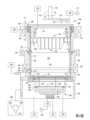
第1圖描繪了根據本揭露的至少一些實施例的處理腔室100(例如,電漿處理腔室)的示意性側視圖。在一些實施例中,處理腔室100是適於在具有給定直徑的基板上濺射沉積材料的PVD處理腔室。適於受益於本揭露的合適的PVD腔室的說明性實例包括可從加利福尼亞州聖克拉拉市的應用材料公司(Applied Materials, Inc., of Santa Clara, California)購得的彼等。可從應用材料公司以及其他製造商獲得的其他處理腔室亦可以根據本文所述的實施例進行修改。FIG. 1 depicts a schematic side view of a processing chamber 100 (eg, a plasma processing chamber) according to at least some embodiments of the present disclosure. In some embodiments, the
處理腔室100通常包括上側壁102、下側壁103、接地適配器104和蓋組件111,從而限定了封閉內部體積106的主體105。適配器板107可以設置在上側壁102與下側壁103之間。The
基板支撐件108設置在處理腔室100的內部體積106中。基板支撐件108被配置為支撐具有給定直徑(例如,150 mm、200 mm、300 mm、450 mm等)的基板。基板轉移埠109形成在下側壁103中以用於將基板轉移到內部體積106中及從該內部體積轉移出。A
氣體源110耦接至處理腔室100,以將處理氣體供應至內部體積106中。若需要,則製程氣體可包括惰性氣體、非反應性氣體及反應性氣體。可由氣體源110提供的處理氣體的實例包括但不限於氬氣(Ar)、氦氣(He)、氖氣(Ne)、氮氣(N2)、氧氣(O2)和水(H2O)蒸汽、其他稀有氣體等。A
泵送裝置112耦接至與內部體積106連通的處理腔室100,以控制內部體積106的壓力。在至少一些實施例中,在沉積期間,處理腔室100的壓力位準可維持在約1毫托至約1托,例如約300毫托至約500毫托。A
接地適配器104可支撐靶標,諸如靶標114。靶標114由待沉積在基板上的材料製成。在至少一些實施例中,靶標114可由鋁(Al)、鈷(Co)、銅(Cu)、鎳(Ni)、鉭(Ta)、鈦(Ti)、鎢(W)、其合金、其組合等製成。在至少一些實施例中,處理腔室100被配置為在基板上沉積例如氧化鋁(AlO2)、氧氮化鋁(諸如ALON)、Co、Cu、Ta、氮化鉭(TaN)、氧氮化鉭(TaOxNy)、Ti、氧氮化鈦(TiOxNy)、W、或氮化鎢(WN)。
靶標114可以耦接至包括用於靶標114的電源117的源組件。例如,電源117可以是RF電源,其可以經由匹配網路116耦接至靶標114。在一些實施例中,電源117可以替代地是DC電源,在此種情況下,匹配網路116被省略。在一些實施例中,電源117可包括DC電源及RF電源兩者。此外,在一些實施例中,靶標114可包括背板(第1圖中未圖示),該背板可被提供用於提高靶標114的結構穩定性。該背板可包含導電材料,諸如銅-鋅、銅-鉻、或與靶標114相同的材料,使得RF和視情況DC功率可經由該背板耦接至靶標114。或者,背板可以是非導電的,並且可以包括導電元件(未圖示),諸如電氣饋通等。The
磁控管170位於靶標114上方,並且可包括一或多個磁體172,該等磁體172可沿路徑旋轉,由連接到軸176的基底板174支撐,該軸可與處理腔室100和基板101的中心軸線軸向對準。一或多個磁體172在處理腔室100內靠近靶標114的正面產生磁場以產生電漿165,因此大通量的離子流撞擊靶標114,從而導致靶材料的濺射發射。一或多個磁體172可以圍繞軸176旋轉,以增加跨靶標114的表面的磁場的均勻性。通常,一或多個磁體172可經旋轉,使得在該一或多個磁體172的旋轉期間最內部的磁體位置設置在正在被處理的基板的直徑上方或外部(例如,從旋轉軸線至該一或多個磁體172的最內部位置的距離等於或大於正在被處理的基板的直徑)。Magnetron 170 is positioned above
準直器118可位於靶標114與基板支撐件108之間的內部體積106中。準直器118的中心區域135通常對應於正在被處理的基板的直徑(例如,等於或基本上等於該基板的直徑)。因此,準直器118的周邊區域133通常對應於在正被處理的基板的徑向外側的環形區域(例如,周邊區域133的內部直徑基本上等於或大於基板的直徑)。在一些實施例中,準直器118可經電偏置以控制到基板的離子通量及基板處的中性角分佈,以及由於增加的DC偏置而增加沉積速率。A
準直器118耦接至上部遮蔽件113,該上部遮蔽件繼而耦接至處理工具適配器138。處理工具適配器138可以由與處理腔室100中的處理條件相容的合適的導電材料製成。絕緣環156和絕緣環157設置在處理工具適配器138的兩側上,以將處理工具適配器138與接地適配器104電絕緣。絕緣環156、157可以由合適的處理相容的介電材料製成。The
在至少一些實施例中,第一組磁體196可設置成與接地適配器104相鄰,以幫助產生磁場,從而引導從靶標114逐出的離子穿過周邊區域133。在至少一些實施例中,第二組磁體194可以設置在某一位置以在準直器118的底部與基板之間形成磁場,從而引導從靶標114逐出的金屬離子並將該等離子更均勻地分佈在基板101上方。在至少一些實施例中,第三組磁體154可以設置在第一組磁體196與第二組磁體194之間,並且大致以準直器118的中心區域135的面向基板的表面為中心或者在該表面下方,以進一步將金屬離子導向基板101的中心。In at least some embodiments, a first set of
處理工具適配器138包括一或多個特徵,以促進支撐內部體積106內的處理工具,諸如準直器118。例如,如第1圖所示,處理工具適配器138包括安裝環或擱架164,該安裝環或擱架沿徑向向內方向延伸以支撐上部遮蔽件113。
在一些實施例中,可在處理工具適配器138中提供冷卻劑通道166,以促進冷卻劑流過處理工具適配器138,從而移除處理期間產生的熱量。例如,冷卻劑通道166可以耦接至冷卻設備153(冷卻劑源)以提供合適的冷卻劑,諸如水(去離子水)、氮氣、氬氣或其他稀有氣體、清潔乾燥空氣(clean dry air, CDA)或腐蝕性氣體等。冷卻劑通道166有利地從處理工具(例如,準直器118)移除不容易傳遞到其他冷卻腔室部件(諸如接地適配器104)的熱量。In some embodiments,
提供徑向向內延伸的凸耳(例如,安裝環或擱板164)以支撐處理腔室100的內部體積106內的中央開口內的上部遮蔽件113。擱板164可以設置在靠近冷卻劑通道166的位置,以促進在使用期間最大化從準直器118至冷卻劑通道166中流動的冷卻劑的熱傳遞。Radially inwardly extending ledges (eg, mounting rings or shelves 164 ) are provided to support the
可在準直器118附近和接地適配器104或上側壁102的內部提供下部遮蔽件120。下部遮蔽件120可包括管狀主體121,該管狀主體具有設置在管狀主體121的上表面中的徑向向外延伸的凸緣122。凸緣122提供了與上側壁102的上表面的配合界面。下部遮蔽件120的管狀主體121可以包括肩部區域123,該肩部區域的內徑小於管狀主體121的其餘部分的內徑。管狀主體121的內表面沿著錐形表面124徑向向內過渡到肩部區域123的內表面。A
遮蔽件環126可設置在處理腔室100中,與下部遮蔽件120相鄰並位於下部遮蔽件120與適配器板107的中間。遮蔽件環126可以至少部分地設置在由下部遮蔽件120的肩部區域123的相對兩側和適配器板107的內側壁形成的凹槽128中。遮蔽件環126可以包括軸向突出的環形側壁127,該軸向突出的環形側壁的內部直徑大於下部遮蔽件120的肩部區域123的外部直徑。A
徑向凸緣130從環形側壁127延伸。徑向凸緣130包括在徑向凸緣130的下表面上形成的突起132。突起132可以是從徑向凸緣130的表面以基本上平行於遮蔽件環126的環形側壁127的內部直徑表面的取向延伸的圓形脊。突起132通常適於與設置在基板支撐件108上的邊緣環136中形成的凹槽134配合。凹槽134可以是形成在邊緣環136中的圓形凹槽。突起132和凹槽134的接合使遮蔽件環126相對於基板支撐件108的縱軸居中。藉由基板支撐件108與機器人葉片(未圖示)之間的協同定位校準,基板101(圖示為支撐在升降銷140上)相對於基板支撐件108的縱向軸線居中。
RF電源180可經由基板支撐件108耦接至處理腔室100,以在靶標114與基板支撐件108之間提供偏壓功率。在一些實施例中,匹配網路(例如,匹配網路116)可以耦接在RF電源180與基板支撐件108之間。RF電源180可以具有在約400 Hz與約60 MHz之間,諸如約13.56 MHz的頻率。An
在操作中,其上設置有基板101的機器人葉片(未圖示)延伸穿過基板轉移埠109。基板支撐件108可以經降低以允許將基板101轉移到從基板支撐件108延伸的升降銷140。基板支撐件108和/或升降銷140的提升及降低可由耦接至基板支撐件108的驅動器142控制。基板101可以被降低到基板支撐件108的基板接收表面144上。隨著基板101定位在基板支撐件108的基板接收表面144上,可以在基板101上執行濺射沉積。在處理期間,邊緣環136可以與基板101電絕緣。In operation, a robot blade (not shown) on which the
在濺射沉積後,可利用升降銷140將基板101提升至與基板支撐件108間隔開的位置。升高的位置可以接近鄰近適配器板107的遮蔽件環126和反射環148中的一或兩者。適配器板107包括一或多個燈150,該一或多個燈在反射器環148的下表面與適配器板107的凹陷表面152中間的位置處耦接至適配器板107。燈150提供可見光或近可見光波長的光能及/或輻射能,諸如紅外(infrared, IR)及/或紫外(ultraviolet, UV)光譜。來自燈150的能量朝向基板101的背面(亦即,下表面)徑向向內聚焦,以加熱基板101及沉積在該基板上的材料。After sputter deposition, the
在將基板101控制到預定溫度之後,將基板101降低到基板支撐件108的基板接收表面144上的位置。可以利用基板支撐件108中的熱控制通道146經由傳導快速冷卻基板101。例如,冷卻設備153可以連接至基板支撐件108,並被配置為向基板支撐件108提供一或多種冷卻劑。基板101可經由基板轉移埠109從處理腔室100移除,以供進一步處理。After controlling the
控制器198耦接至處理腔室100。控制器198包括中央處理單元160、記憶體158和支援電路162。控制器198用於控制製程順序,調節從氣體源110進入處理腔室100的氣體流量,並控制靶標114的離子轟擊。中央處理單元160可以是可以在工業環境中使用的任何形式的通用電腦處理器。軟體常式(例如,指令)可以儲存在記憶體158(例如,非暫時性電腦可讀取儲存媒體),諸如隨機存取記憶體、唯讀記憶體、軟盤或硬碟驅動器或其他形式的數位儲存裝置中。支援電路162習知地耦接至中央處理單元160,並且可包括快取、時鐘電路、輸入/輸出子系統、電源等。當由中央處理單元160執行時,軟體常式將中央處理單元轉換成控制處理腔室100的專用電腦,使得根據本揭露的實施例執行包括下面揭示的基板支撐件108冷卻製程在內的製程。軟體常式也可以由遠離處理腔室100定位的第二控制器(未圖示)儲存及/或執行。A
在處理期間,材料從靶標114濺射並沉積在基板101的表面上。靶標114及基板支撐件108由電源117或RF電源180相對於彼此偏置,以維持從由氣體源110供應的處理氣體形成的電漿。施加到準直器118的DC脈衝偏壓功率亦有助於控制穿過準直器118的離子和中性粒子的比率,從而有利地增強溝槽側壁和底部填充能力。來自電漿的離子朝向靶標114加速並撞擊該靶標,從而導致靶材料被從靶標114中逐出。被逐出的靶材料及處理氣體在基板101上形成具有所需組成的層。During processing, material is sputtered from the
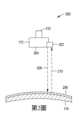
第2圖是根據本揭露的至少一些實施例,被配置用於與第1圖的處理腔室100一起使用的磁體至靶標間距系統200的示意圖。例如,磁體至靶標間距系統200包括感測器202,該感測器被配置為在相對於靶標旋轉磁體的同時提供同磁體(例如,一或多個磁體172)的正面204與靶標(例如,靶標114)的背面206之間的距離相對應的信號。感測器202可以是能夠發射和接收射束的任何感測器。例如,在至少一些實施例中,感測器202是雷射感測器,該雷射感測器被配置用於朝向靶標的背面206發射偵測射束208,並從靶標的背面206接收反射射束210。感測器202可以經由一或多個合適的耦接設備耦接至磁體的一或多個區域。例如,在所示實施例中,感測器202經由一或多個螺釘、螺母、螺栓等耦接至磁體的側表面。FIG. 2 is a schematic diagram of a magnet-to-
靶標間距系統200亦包括磁體控制器212(例如,控制器198),該磁體控制器通訊耦合(有線或無線)至感測器202,被配置為基於由感測器202提供的信號來控制磁體的正面204與靶標的背面206之間的距離。例如,磁體控制器212被配置為基於偵測射束208的行進速度、從發射偵測射束208時到接收反射射束210時的時間變化、以及固定純量值(例如,0.5的固定純量值)來確定磁體的正面204與靶標的背面206之間的距離變化。例如,磁體的正面204與靶標的背面206之間的距離變化可以使用以下等式來計算: 距離變化=0.5*Δt*V射束,(1) 其中V射束=偵測射束208的行進速度,Δt=從發射偵測射束208時到接收反射射束210時的時間變化,並且0.5是固定純量值。在至少一些實施例中,在操作期間,磁體的正面24與靶標的背面206之間的距離變化可以是約2.75 mm至約3.25 mm。
第3圖是根據本揭露的至少一些實施例,被配置用於與第1圖的處理腔室100一起使用的磁體至靶標間距系統300的示意圖。第3圖的靶標間距系統300基本上類似於第2圖的靶標間距系統200。因此,本文僅描述靶標間距系統300所獨有的彼等特徵。例如,如上所述,磁控管170可以包括一或多個磁體172,該一或多個磁體可以耦接至基底板174。因此,靶標間距系統300包括兩個或更多個磁體172(第3圖中圖示為兩個),該兩個或更多個磁體包括感測器202和磁體控制器212。在第3圖的實施例中,該兩個磁體中的一個磁體設置為鄰近靶標114的中心(在該中心上方),並且該兩個磁體中的另一個磁體可設置為鄰近靶標114的周邊邊緣(在該周邊邊緣上方),該周邊邊緣通常是靶標彎曲更頻繁發生的地方。FIG. 3 is a schematic illustration of a magnet-to-
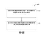
第4圖是根據本揭露的至少一些實施例的用於處理基板的方法400的流程圖。例如,在PVD期間,磁控管170可以經由軸176旋轉一或多個磁體172,以在處理腔室100內靠近靶標114的正面產生磁場以產生電漿,因此大通量的離子流撞擊靶標114,從而導致靶材料的濺射發射。FIG. 4 is a flowchart of a
在402處,方法400包括在相對於靶標旋轉磁體的同時,偵測磁體的正面與靶標的背面之間的距離。例如,在402處,在旋轉一或多個磁體172的同時,磁體控制器212可以偵測一或多個磁體172的正面204與靶標114的背面206之間的距離。例如,感測器202可以朝向靶標114的背面206發射偵測射束208。接下來,磁體控制器212可以從靶標114的背面206接收反射射束。磁體控制器212可以偵測一或多個磁體172的正面204與靶標的背面206之間的間距是否已經改變。例如,一或多個磁體172的正面204與靶標114的背面206之間的距離變化是基於偵測射束208的行進速度、從發射偵測射束208時到接收反射射束210時的時間變化、以及固定純量值(例如,固定純量值可以是0.5)。如上所述,在至少一些實施例中,磁體的正面204與靶標114的背面206之間的距離可以使用等式(1)來計算。At 402,
接下來,在404處,方法400包括基於所偵測到的距離將一或多個磁體172的正面204與靶標1147的背面206之間的距離控制到期望值。例如,當磁體控制器212確定一或多個磁體172的正面204與靶標114的背面206之間的距離已改變時,磁體控制器212控制器可以向連接到磁控管的軸176的磁體驅動組件(未圖示)發送命令信號,以向上或向下移動軸176(例如,以移動一或多個磁體的正面204遠離或更靠近靶標114的背面206)。例如,如第3圖所示,當例如由於靶標彎曲(d1小於d2),一或多個磁體172的正面204與靶標114的背面206之間的距離已經增加時,則磁體控制器212可以向磁體驅動組件發送命令信號,以向下移動軸176,例如更靠近靶標114的背面206,以維持一或多個磁體172的正面204與靶標114的背面206之間的一致距離(例如,d3=d1)。Next, at 404 ,
儘管前面是針對本揭露案的實施例,但是在不脫離本揭露案的基本範疇的情況下,可以設計本揭露案的其他及進一步的實施例。While the foregoing is directed to embodiments of the disclosure, other and further embodiments of the disclosure can be devised without departing from the basic scope of the disclosure.
100:處理腔室 101:基板 102:上側壁 103:下側壁 104:接地適配器 105:主體 106:內部體積 107:適配器板 108:基板支撐件 109:基板轉移埠 110:氣體源 111:蓋組件 112:泵送裝置 113:上部遮蔽件 114:靶標 116:匹配網路 117:電源 118:準直器 120:下部遮蔽件 121:管狀主體 122:凸緣 123:肩部區域 124:錐形表面 126:遮蔽件環 127:環形側壁 128:凹槽 130:徑向凸緣 132:突起 133:周邊區域 134:凹槽 135:中心區域 136:邊緣環 138:處理工具適配器 140:升降銷 142:驅動器 144:基板接收表面 146:熱控制通道 148:反射環 150:燈 152:凹陷表面 153:冷卻設備 154:第三組磁體 156:絕緣環 157:絕緣環 158:記憶體 160:中央處理單元 162:支援電路 164:擱板 165:電漿 166:冷卻劑通道 170:磁控管 172:磁體 174:基底板 176:軸 180:RF電源 194:第二組磁體 196:第一組磁體 198:控制器 200:磁體至靶標間距系統 202:感測器 204:正面 206:背面 208:偵測射束 210:反射射束 212:磁體控制器 300:磁體至靶標間距系統 400:方法 402:步驟 404:步驟 d1:距離 d2:距離 d3:距離100: processing chamber 101: Substrate 102: upper side wall 103: lower side wall 104: Grounding adapter 105: subject 106: Internal volume 107: Adapter board 108: substrate support 109: substrate transfer port 110: gas source 111: cover assembly 112: Pumping device 113: upper shield 114: target 116:Matching network 117: power supply 118: Collimator 120: lower cover 121: Tubular body 122: Flange 123: Shoulder area 124: conical surface 126: Cover ring 127: Annular side wall 128: Groove 130: radial flange 132:Protrusion 133: Surrounding area 134: Groove 135: Central area 136: edge ring 138: Processing Tool Adapter 140:Lift pin 142: drive 144: substrate receiving surface 146: thermal control channel 148: reflection ring 150: light 152: concave surface 153: cooling equipment 154: The third group of magnets 156: insulating ring 157: insulating ring 158: memory 160: central processing unit 162: support circuit 164: shelf 165: Plasma 166: Coolant channel 170: Magnetron 172: magnet 174: base plate 176: Shaft 180: RF power supply 194: Second set of magnets 196: The first set of magnets 198: Controller 200: Magnet to target distance system 202: sensor 204: front 206: back 208: Detection Beam 210: Reflected Beam 212:Magnet controller 300: Magnet to target distance system 400: method 402: step 404: step d1: distance d2: distance d3: distance
藉由參考附圖中描繪的本揭露案的說明性實施例,可以理解上面簡要總結並且下面更詳細論述的本揭露案的實施例。然而,附圖僅圖示了本揭露的典型實施例,因此不應被認為是對範疇的限制,因為本揭露案可以允許其他同等有效的實施例。Embodiments of the disclosure, briefly summarized above and discussed in greater detail below, can be understood by reference to the illustrative embodiments of the disclosure depicted in the accompanying drawings. However, the drawings illustrate only typical embodiments of the disclosure and are therefore not to be considered limiting of scope, for the disclosure may admit to other equally effective embodiments.
第1圖係根據本揭露的至少一些實施例的處理腔室的示意性剖視圖。FIG. 1 is a schematic cross-sectional view of a processing chamber according to at least some embodiments of the present disclosure.
第2圖係根據本揭露的至少一些實施例,被配置用於與第1圖的處理腔室一起使用的磁體至靶標間距系統的圖式。FIG. 2 is a diagram of a magnet-to-target spacing system configured for use with the processing chamber of FIG. 1, in accordance with at least some embodiments of the present disclosure.
第3圖係根據本揭露的至少一些實施例,被配置用於與第1圖的處理腔室一起使用的磁體至靶標間距系統的圖式。FIG. 3 is a diagram of a magnet-to-target spacing system configured for use with the processing chamber of FIG. 1 , according to at least some embodiments of the present disclosure.
第4圖是根據本揭露的至少一些實施例的用於處理基板的方法的流程圖。FIG. 4 is a flowchart of a method for processing a substrate according to at least some embodiments of the present disclosure.
為了促進理解,在可能的情況下,使用相同的附圖標記來表示附圖中共用的元件。附圖不是按比例繪製的,並且為了清楚起見可以簡化。一個實施例的元件和特徵可以有益地結合到其他實施例中,而無需進一步敘述。To facilitate understanding, the same reference numerals have been used, where possible, to denote elements that are common to the figures. The figures are not drawn to scale and may be simplified for clarity. Elements and features of one embodiment may be beneficially incorporated in other embodiments without further recitation.
國內寄存資訊(請依寄存機構、日期、號碼順序註記) 無 國外寄存資訊(請依寄存國家、機構、日期、號碼順序註記) 無Domestic deposit information (please note in order of depositor, date, and number) none Overseas storage information (please note in order of storage country, institution, date, and number) none
114:靶標114: target
172:磁體172: magnet
200:磁體至靶標間距系統200: Magnet to target distance system
202:感測器202: sensor
204:正面204: front
206:背面206: back
208:偵測射束208: Detection Beam
210:反射射束210: Reflected Beam
212:磁體控制器212:Magnet controller
Claims (20)
Translated fromChineseApplications Claiming Priority (2)
| Application Number | Priority Date | Filing Date | Title |
|---|---|---|---|
| US17/329,796 | 2021-05-25 | ||
| US17/329,796US11761078B2 (en) | 2021-05-25 | 2021-05-25 | Methods and apparatus for processing a substrate |
Publications (1)
| Publication Number | Publication Date |
|---|---|
| TW202307911Atrue TW202307911A (en) | 2023-02-16 |
Family
ID=84193835
Family Applications (1)
| Application Number | Title | Priority Date | Filing Date |
|---|---|---|---|
| TW111118370ATW202307911A (en) | 2021-05-25 | 2022-05-17 | Methods and apparatus for processing a substrate |
Country Status (5)
| Country | Link |
|---|---|
| US (1) | US11761078B2 (en) |
| KR (1) | KR20240013165A (en) |
| CN (1) | CN117396631A (en) |
| TW (1) | TW202307911A (en) |
| WO (1) | WO2022250936A1 (en) |
Families Citing this family (1)
| Publication number | Priority date | Publication date | Assignee | Title |
|---|---|---|---|---|
| WO2023018596A1 (en)* | 2021-08-12 | 2023-02-16 | Lam Research Corporation | Process module chamber providing symmetric rf return path |
Family Cites Families (12)
| Publication number | Priority date | Publication date | Assignee | Title |
|---|---|---|---|---|
| JPH10227857A (en)* | 1997-02-14 | 1998-08-25 | Nikon Corp | Lightwave ranging device |
| KR20010001581A (en) | 1999-06-07 | 2001-01-05 | 윤종용 | Plasma pattern variable sputtering apparatus with rotating magnetic field |
| WO2005007924A1 (en) | 2003-07-07 | 2005-01-27 | Honeywell International Inc. | Sputtering target constructions |
| US20050133361A1 (en)* | 2003-12-12 | 2005-06-23 | Applied Materials, Inc. | Compensation of spacing between magnetron and sputter target |
| EP1908090B1 (en)* | 2004-09-28 | 2012-11-28 | OC Oerlikon Balzers AG | Method for the production of magnetron-coated substrates and magnetron sputter source |
| US8778144B2 (en)* | 2004-09-28 | 2014-07-15 | Oerlikon Advanced Technologies Ag | Method for manufacturing magnetron coated substrates and magnetron sputter source |
| US8137519B2 (en)* | 2008-03-13 | 2012-03-20 | Canon Anelva Corporation | Sputtering cathode, sputtering apparatus provided with sputtering cathode, film-forming method, and method for manufacturing electronic device |
| KR101009642B1 (en)* | 2008-07-09 | 2011-01-19 | 삼성모바일디스플레이주식회사 | Magnetron subconveying device for preventing magnetization and magnetron sputtering equipment having the same |
| US8070925B2 (en) | 2008-10-17 | 2011-12-06 | Applied Materials, Inc. | Physical vapor deposition reactor with circularly symmetric RF feed and DC feed to the sputter target |
| US8795487B2 (en)* | 2010-03-31 | 2014-08-05 | Applied Materials, Inc. | Physical vapor deposition chamber with rotating magnet assembly and centrally fed RF power |
| JP2020169352A (en)* | 2019-04-02 | 2020-10-15 | 株式会社アルバック | Cathode unit for magnetron sputtering apparatus |
| CN111146117A (en) | 2019-12-10 | 2020-05-12 | 华虹半导体(无锡)有限公司 | Wafer movement monitoring method and glue spreading developing machine |
- 2021
- 2021-05-25USUS17/329,796patent/US11761078B2/enactiveActive
- 2022
- 2022-05-09CNCN202280036113.XApatent/CN117396631A/enactivePending
- 2022-05-09KRKR1020237044242Apatent/KR20240013165A/enactivePending
- 2022-05-09WOPCT/US2022/028269patent/WO2022250936A1/ennot_activeCeased
- 2022-05-17TWTW111118370Apatent/TW202307911A/enunknown
Also Published As
| Publication number | Publication date |
|---|---|
| US20220380883A1 (en) | 2022-12-01 |
| WO2022250936A1 (en) | 2022-12-01 |
| US11761078B2 (en) | 2023-09-19 |
| KR20240013165A (en) | 2024-01-30 |
| CN117396631A (en) | 2024-01-12 |
Similar Documents
| Publication | Publication Date | Title |
|---|---|---|
| KR102383703B1 (en) | Methods and apparatus for controlling ion fraction in physical vapor deposition processes | |
| US10312065B2 (en) | Physical vapor deposition (PVD) plasma energy control per dynamic magnetron control | |
| TW202301421A (en) | Methods and apparatus for processing a substrate | |
| TW202307911A (en) | Methods and apparatus for processing a substrate | |
| WO2022177916A1 (en) | Substrate temperature non-uniformity reduction over target life using spacing compensation | |
| KR20230023602A (en) | Methods and apparatus for semi-dynamic bottom-up reflow | |
| US11952655B2 (en) | Electromagnet pulsing effect on PVD step coverage | |
| US20230017383A1 (en) | Methods and apparatus for processing a substrate | |
| US11784033B2 (en) | Methods and apparatus for processing a substrate | |
| US11981989B2 (en) | Automated temperature controlled substrate support | |
| TW202446978A (en) | Biased or floating process shield for a substrate processing chamber | |
| TW202426676A (en) | Power compensation in pvd chambers |