TW202304137A - Dynamic cross-coupled regeneration for high-speed sense amplifier - Google Patents
Dynamic cross-coupled regeneration for high-speed sense amplifierDownload PDFInfo
- Publication number
- TW202304137A TW202304137ATW111116285ATW111116285ATW202304137ATW 202304137 ATW202304137 ATW 202304137ATW 111116285 ATW111116285 ATW 111116285ATW 111116285 ATW111116285 ATW 111116285ATW 202304137 ATW202304137 ATW 202304137A
- Authority
- TW
- Taiwan
- Prior art keywords
- transistor
- input
- circuit
- coupled
- output
- Prior art date
Links
- 230000008929regenerationEffects0.000titleclaimsabstractdescription73
- 238000011069regeneration methodMethods0.000titleclaimsabstractdescription73
- 230000001172regenerating effectEffects0.000claimsdescription114
- 238000000034methodMethods0.000claimsdescription33
- 230000008878couplingEffects0.000claimsdescription25
- 238000010168coupling processMethods0.000claimsdescription25
- 238000005859coupling reactionMethods0.000claimsdescription25
- 230000007704transitionEffects0.000claimsdescription11
- 230000005669field effectEffects0.000claimsdescription7
- 238000012360testing methodMethods0.000claimsdescription2
- 239000002184metalSubstances0.000description15
- 230000000295complement effectEffects0.000description9
- 238000006880cross-coupling reactionMethods0.000description6
- 230000005540biological transmissionEffects0.000description4
- 238000010586diagramMethods0.000description3
- 230000000694effectsEffects0.000description3
- 230000009467reductionEffects0.000description3
- 230000035945sensitivityEffects0.000description3
- 230000008901benefitEffects0.000description2
- 230000007423decreaseEffects0.000description2
- 238000012986modificationMethods0.000description2
- 230000004048modificationEffects0.000description2
- 238000011084recoveryMethods0.000description2
- 238000004891communicationMethods0.000description1
- 230000001419dependent effectEffects0.000description1
- 230000000737periodic effectEffects0.000description1
- 238000012545processingMethods0.000description1
- 239000004065semiconductorSubstances0.000description1
- 239000000758substrateSubstances0.000description1
- 238000012546transferMethods0.000description1
Images


Classifications
- G—PHYSICS
- G11—INFORMATION STORAGE
- G11C—STATIC STORES
- G11C7/00—Arrangements for writing information into, or reading information out from, a digital store
- G11C7/06—Sense amplifiers; Associated circuits, e.g. timing or triggering circuits
- G11C7/065—Differential amplifiers of latching type
- G—PHYSICS
- G11—INFORMATION STORAGE
- G11C—STATIC STORES
- G11C7/00—Arrangements for writing information into, or reading information out from, a digital store
- G11C7/06—Sense amplifiers; Associated circuits, e.g. timing or triggering circuits
- G11C7/08—Control thereof
- H—ELECTRICITY
- H03—ELECTRONIC CIRCUITRY
- H03K—PULSE TECHNIQUE
- H03K5/00—Manipulating of pulses not covered by one of the other main groups of this subclass
- H03K5/22—Circuits having more than one input and one output for comparing pulses or pulse trains with each other according to input signal characteristics, e.g. slope, integral
- H03K5/24—Circuits having more than one input and one output for comparing pulses or pulse trains with each other according to input signal characteristics, e.g. slope, integral the characteristic being amplitude
- H03K5/2472—Circuits having more than one input and one output for comparing pulses or pulse trains with each other according to input signal characteristics, e.g. slope, integral the characteristic being amplitude using field effect transistors
- H03K5/2481—Circuits having more than one input and one output for comparing pulses or pulse trains with each other according to input signal characteristics, e.g. slope, integral the characteristic being amplitude using field effect transistors with at least one differential stage
- H—ELECTRICITY
- H03—ELECTRONIC CIRCUITRY
- H03M—CODING; DECODING; CODE CONVERSION IN GENERAL
- H03M9/00—Parallel/series conversion or vice versa
- G—PHYSICS
- G11—INFORMATION STORAGE
- G11C—STATIC STORES
- G11C2207/00—Indexing scheme relating to arrangements for writing information into, or reading information out from, a digital store
- G11C2207/002—Isolation gates, i.e. gates coupling bit lines to the sense amplifier
- G—PHYSICS
- G11—INFORMATION STORAGE
- G11C—STATIC STORES
- G11C2207/00—Indexing scheme relating to arrangements for writing information into, or reading information out from, a digital store
- G11C2207/005—Transfer gates, i.e. gates coupling the sense amplifier output to data lines, I/O lines or global bit lines
- G—PHYSICS
- G11—INFORMATION STORAGE
- G11C—STATIC STORES
- G11C2207/00—Indexing scheme relating to arrangements for writing information into, or reading information out from, a digital store
- G11C2207/06—Sense amplifier related aspects
- G11C2207/063—Current sense amplifiers
- G—PHYSICS
- G11—INFORMATION STORAGE
- G11C—STATIC STORES
- G11C7/00—Arrangements for writing information into, or reading information out from, a digital store
- G11C7/06—Sense amplifiers; Associated circuits, e.g. timing or triggering circuits
- G11C7/062—Differential amplifiers of non-latching type, e.g. comparators, long-tailed pairs
- G—PHYSICS
- G11—INFORMATION STORAGE
- G11C—STATIC STORES
- G11C7/00—Arrangements for writing information into, or reading information out from, a digital store
- G11C7/10—Input/output [I/O] data interface arrangements, e.g. I/O data control circuits, I/O data buffers
- G11C7/1078—Data input circuits, e.g. write amplifiers, data input buffers, data input registers, data input level conversion circuits
- G11C7/1084—Data input buffers, e.g. comprising level conversion circuits, circuits for adapting load
- H—ELECTRICITY
- H03—ELECTRONIC CIRCUITRY
- H03K—PULSE TECHNIQUE
- H03K5/00—Manipulating of pulses not covered by one of the other main groups of this subclass
- H03K5/22—Circuits having more than one input and one output for comparing pulses or pulse trains with each other according to input signal characteristics, e.g. slope, integral
- H03K5/24—Circuits having more than one input and one output for comparing pulses or pulse trains with each other according to input signal characteristics, e.g. slope, integral the characteristic being amplitude
- H03K5/2472—Circuits having more than one input and one output for comparing pulses or pulse trains with each other according to input signal characteristics, e.g. slope, integral the characteristic being amplitude using field effect transistors
- H03K5/249—Circuits having more than one input and one output for comparing pulses or pulse trains with each other according to input signal characteristics, e.g. slope, integral the characteristic being amplitude using field effect transistors using clock signals
Landscapes
- Physics & Mathematics (AREA)
- Nonlinear Science (AREA)
- Engineering & Computer Science (AREA)
- Theoretical Computer Science (AREA)
- Amplifiers (AREA)
- Dram (AREA)
- Static Random-Access Memory (AREA)
- Manipulation Of Pulses (AREA)
Abstract
Description
Translated fromChinese本申請主張於2021年05月14日在美國專利商標局提交的非臨時申請序號17/321,005的優先權和權益。This application claims priority and benefit to non-provisional application serial number 17/321,005 filed in the United States Patent and Trademark Office on May 14, 2021.
本公開內容的方面總體上涉及放大器,並且更具體地涉及感測放大器。Aspects of this disclosure relate generally to amplifiers, and more specifically to sense amplifiers.
感測放大器被用於廣泛的應用中,應用包括高速串聯器/解串器(SerDes)中的資料採樣器、記憶體和類比數位元轉換器。在資料採樣器的情況下,感測放大器可以包括再生電路,再生電路向感測放大器提供再生反饋以快速解析資料採樣器中的傳入資料位元。期望增加再生電路的再生增益以增加感測放大器的速度和靈敏度。Sense amplifiers are used in a wide variety of applications including data samplers in high-speed serializer/deserializers (SerDes), memory and analog-to-digital converters. In the case of a data sampler, the sense amplifier may include a regenerative circuit that provides regenerative feedback to the sense amplifier to quickly resolve incoming data bits in the data sampler. It is desirable to increase the regeneration gain of the regeneration circuit to increase the speed and sensitivity of the sense amplifier.
以下示出一個或多個實施方式的簡化總結,以便提供對這些實施方式的基本理解。所述發明內容不是對所有預期實施方式的廣泛概述,並且既不旨在識別所有實施方式的關鍵或重要元素,也不旨在描述任何或所有實施方式的範圍。其唯一目的是以簡化形式示出一個或多個實施方式的一些概念,作為稍後示出的更詳細描述的序言。A simplified summary of one or more implementations is presented below in order to provide a basic understanding of these implementations. This summary is not an extensive overview of all contemplated implementations, and is intended to neither identify key or critical elements of all implementations nor delineate the scope of any or all implementations. Its sole purpose is to present some concepts of one or more implementations in a simplified form as a prelude to the more detailed description that is presented later.
第一方面涉及一種再生電路。再生電路包括具有輸入和輸出的第一反相電路,並且包括具有輸入和輸出的第二反相電路。再生電路還包括耦接到第二反相電路的輸入的第一電晶體,其中第一電晶體的閘極被配置成接收第一輸入信號,並且還包括耦接到第一反相電路的輸入的第二電晶體,其中第二電晶體的閘極被配置成接收第二輸入信號。再生電路還包括耦接在第一電晶體和第一反相電路的輸出之間的第一開關,其中第一開關的控制輸入被配置成接收時序信號,並且還包括耦接在第二電晶體和第二反相電路的輸出之間的第二開關,其中第二開關的控制輸入被配置成接收所述時序信號。The first aspect relates to a regenerative circuit. The regenerative circuit includes a first inverting circuit having an input and an output, and includes a second inverting circuit having an input and an output. The regenerative circuit also includes a first transistor coupled to an input of the second inverting circuit, wherein the gate of the first transistor is configured to receive the first input signal, and further includes an input coupled to the first inverting circuit The second transistor, wherein the gate of the second transistor is configured to receive the second input signal. The regenerative circuit also includes a first switch coupled between the first transistor and the output of the first inverting circuit, wherein the control input of the first switch is configured to receive the timing signal, and further includes a first switch coupled between the second transistor and a second switch between the output of the second inverting circuit, wherein the control input of the second switch is configured to receive the timing signal.
第二方面涉及一種感測放大器。感測放大器包括輸入電路和再生電路。輸入電路包括第一電晶體,其中第一電晶體的閘極被配置成接收第一輸入信號,並且第一電晶體的汲極耦接到輸入電路的第一輸出,並且包括第二電晶體,其中第二電晶體的閘極被配置成接收第二輸入信號,並且第二電晶體的汲極耦接到輸入電路的第二輸出。再生電路包括具有輸入和輸出的第一反相電路,並且包括具有輸入和輸出的第二反相電路。再生電路還包括耦接到第二反相電路的輸入的第三電晶體,其中第三電晶體的閘極耦接到輸入電路的第二輸出,並且還包括耦接到第一反相電路的輸入的第四電晶體,其中第四電晶體的閘極耦接到輸入電路的第一輸出。再生電路還包括耦接在第三電晶體和第一反相電路的輸出之間的第一開關,其中第一開關的控制輸入被配置成接收時序信號,並且還包括耦接在第四電晶體和第二反相電路的輸出之間的第二開關,其中第二開關的控制輸入被配置成接收所述時序信號。A second aspect relates to a sense amplifier. The sense amplifier includes an input circuit and a regeneration circuit. The input circuit includes a first transistor, wherein the gate of the first transistor is configured to receive the first input signal, and the drain of the first transistor is coupled to the first output of the input circuit, and includes a second transistor, Wherein the gate of the second transistor is configured to receive the second input signal, and the drain of the second transistor is coupled to the second output of the input circuit. The regenerative circuit includes a first inverting circuit having an input and an output, and includes a second inverting circuit having an input and an output. The regenerative circuit also includes a third transistor coupled to the input of the second inverting circuit, wherein the gate of the third transistor is coupled to the second output of the input circuit, and further includes a transistor coupled to the first inverting circuit. The input fourth transistor, wherein the gate of the fourth transistor is coupled to the first output of the input circuit. The regenerative circuit further includes a first switch coupled between the third transistor and the output of the first inverting circuit, wherein the control input of the first switch is configured to receive the timing signal, and further includes a fourth transistor coupled to and a second switch between the output of the second inverting circuit, wherein the control input of the second switch is configured to receive the timing signal.
第三方面涉及一種操作感測放大器的再生電路的方法。再生電路包括具有輸入和輸出的第一反相電路、具有輸入和輸出的第二反相電路、耦接到第二反相電路的輸入的第一電晶體,以及耦接到第一反相電路的輸入的第二電晶體。方法包括:在重設階段中,將第一反相電路的輸出與第一電晶體去耦接,以及將第二反相電路的輸出與第二電晶體去耦接。方法還包括:在感測階段中,將第一反相電路的輸出耦接到第一電晶體,以及將第二反相電路的輸出耦接到第二電晶體。A third aspect relates to a method of operating a regeneration circuit of a sense amplifier. The regenerative circuit includes a first inverting circuit having an input and an output, a second inverting circuit having an input and an output, a first transistor coupled to the input of the second inverting circuit, and a first transistor coupled to the first inverting circuit the input of the second transistor. The method includes decoupling the output of the first inverting circuit from the first transistor and decoupling the output of the second inverting circuit from the second transistor during the reset phase. The method also includes, during the sensing phase, coupling the output of the first inverting circuit to the first transistor, and coupling the output of the second inverting circuit to the second transistor.
下面結合圖式闡述的詳細說明旨在作為對各種配置的說明,而不旨在呈現可以實踐本文描述的概念的唯一配置。具體說明包括特定細節,目的是提供對各種概念的透徹理解。然而,對於本領域技術人員來說將明顯的是,可以在沒有這些特定細節的情況下實踐這些概念。在一些情況下,眾所周知的結構和組件以方塊圖形式示出,以避免混淆這種概念。The detailed description set forth below in connection with the drawings is intended as a description of various configurations and is not intended to present the only configurations in which the concepts described herein may be practiced. The detailed description includes specific details for the purpose of providing a thorough understanding of various concepts. It will be apparent, however, to one skilled in the art that these concepts may be practiced without these specific details. In some instances, well-known structures and components are shown in block diagram form in order to avoid obscuring such concepts.
圖1示出了根據本公開內容的某些方面的感測放大器110的示例。例如,感測放大器110可以被用在資料採樣器中,以對傳入的資料位元進行採樣和解析。感測放大器110包括輸入電路115和再生電路140。輸入電路115也可以被稱為輸入級,並且再生電路140也可以被稱為再生級。FIG. 1 illustrates an example of a
輸入電路115包括第一輸入電晶體120、第二輸入電晶體122、第一開關116、第二開關130和第三開關134。第二開關130耦接在供電軌112和第一輸入電晶體120之間,並且第三開關134耦接在供電軌112和第二輸入電晶體122之間。第一輸入電晶體120耦接在第二開關130和節點117之間,並且第二輸入電晶體122耦接在第三開關134和節點117之間。第一開關116耦接在節點117和地114之間。The
在圖1所示的示例中,第一輸入電晶體120利用第一n型場效電晶體(NFET)實現,並且第二輸入電晶體122利用第二NFET實現。在所述示例中,第二開關130耦接在供電軌112和第一輸入電晶體120的汲極之間,並且第一開關116耦接在第一輸入電晶體120的源極和地114之間。此外,第三開關134耦接在供電軌112和第二輸入電晶體122的汲極之間,並且第一開關116耦接在第二輸入電晶體122的源極和地114之間。應當理解,第一輸入電晶體120和第二輸入電晶體122不限於NFET,並且可以利用其他類型的電晶體實現。In the example shown in FIG. 1 , the
輸入電路115被配置成接收包括第一輸入電壓(被標記為“INP”)和第二輸入電壓(被標記為“INN”)的差分輸入信號(例如,差分資料信號)。第一輸入電壓INP被輸入到輸入電路115的第一輸入121,並且第二輸入電壓INN被輸入到輸入電路115的第二輸入123,其中第一輸入121耦接到第一輸入電晶體120的閘極,並且第二輸入123耦接到第二輸入電晶體122的閘極。差分輸入信號可以具有小的差分電壓(即,第一輸入電壓INP和第二輸入電壓INN之間的小差值),其中差分電壓的極性表示位元值。如下面進一步討論的,感測放大器110被配置成將小差分輸入電壓轉換成大差分輸出電壓以解析位元值。The
第一開關116具有由第一時序信號驅動的控制輸入118,第二開關130具有由第一時序信號驅動的控制輸入132,並且第三開關134具有由第一時序信號驅動的控制輸入136。在一個示例中,第一開關116被配置成在第一時序信號為高時導通,並且在第一時序信號為低時關斷,並且第二開關130和第三開關134中的每個開關被配置成在第一時序信號為低時導通,並且在第一時序信號為高時關斷。在圖1所示的示例中,第一時序信號是時鐘信號(被標記為“CLK”)。如本文所使用的,“時鐘信號”是在高邏輯狀態和低邏輯狀態之間振盪的週期性信號。在某些方面,高邏輯狀態(即邏輯狀態1)可以對應於大約等於供電電壓VCC的電壓,並且低邏輯狀態(即邏輯狀態0)可以對應於大約等於地的電壓。The
如本文所使用的,開關的“控制輸入”是基於控制輸入處的信號(例如,信號的電壓)來控制開關的開/關狀態的輸入。對於利用電晶體實現開關的示例,控制輸入位於電晶體的閘極處。As used herein, a "control input" of a switch is an input that controls the on/off state of the switch based on a signal (eg, the voltage of the signal) at the control input. For the example of switching with a transistor, the control input is at the gate of the transistor.
輸入電路115具有位於第二開關130和第一輸入電晶體120之間的節點處的第一輸出124,並且具有位於第三開關134和第二輸入電晶體122之間的節點處的第二輸出126。如下面進一步討論的,第一輸出124處的電壓(被標記為“DINT”)和第二輸出126處的電壓(被標記為“NDINT”)被輸出到再生電路140。在圖1的示例中,第一輸出124耦接到第一輸入電晶體120的汲極,並且第二輸出126耦接到第二輸入電晶體122的汲極。The
再生電路140包括第一輸入電晶體142、第二輸入電晶體146、開關180、第一反相電路150和第二反相電路160。如下面進一步討論的,第一反相電路150和第二反相電路160交叉耦接以提供再生反饋。如本文所使用的,“反相電路”是被配置成對反相電路的輸入處的邏輯狀態(即,邏輯位準或邏輯值)進行反相,並且在反相電路的輸出處輸出反相邏輯狀態的電路。邏輯狀態可以由電壓表示,其中低電壓(例如,接近地)可以表示邏輯狀態0,並且高電壓(例如,接近供電電壓)可以表示邏輯狀態1。在某些方面,反相電路具有閾值電壓,其中當反相電路的輸入處的電壓下降到低於閾值電壓時,反相電路的輸出從低轉換為高,並且當反相電路的輸入處的電壓上升到高於閾值電壓時,反相電路的輸出從高轉換為低。反相電路也可以被稱為反相器、反相電路或另一術語。The
再生電路140具有耦接到輸入電路115的第二輸出126的第一輸入144,並且具有耦接到輸入電路115的第一輸出124的第二輸入148。因此,第一輸入144接收來自輸入電路115的電壓NDINT,並且第二輸入148接收來自輸入電路115的電壓DINT。在這點上,電壓NDINT可以被認為是再生電路140的第一輸入信號,並且電壓DINT可以被認為是再生電路140的第二輸入信號。The
第一反相電路150具有輸入152、輸出154、第一供電端子156和第二供電端子158。第二反相電路160具有輸入162、輸出164、第一供電端子166和第二供電端子168。為了將第一反相電路150和第二反相電路160交叉耦接,第一反相電路150的輸入152耦接到第二反相電路160的輸出164,並且第二反相電路160的輸入162耦接到第一反相電路150的輸出154。第一反相電路150和第二反相電路160的交叉耦接為再生電路140提供再生反饋。再生反饋允許再生電路140實現再生以快速解析資料位元的值,如下面進一步討論的。The
第一反相電路150的第一供電端子156和第二反相電路160的第一供電端子166耦接到供電節點185。第一反相電路150的第二供電端子158和第二反相電路160的第二供電端子168耦接到地114。在所述示例中,再生電路140的第一輸出170耦接到第二反相電路160的輸出164,並且再生電路140的第二輸出175耦接到第一反相電路150的輸出154。The
第一輸入電晶體142耦接在第一反相電路150的輸出154和地114之間。第一輸入電晶體142的閘極耦接到再生電路140的第一輸入144。因此,第一輸入電晶體142的閘極被配置成接收電壓NDINT(即,再生電路140的第一輸入信號)。在一個示例中,第一輸入電晶體142被配置成在電壓NDINT高於第一輸入電晶體142的閾值電壓時導通,並且在電壓NDINT低於第一輸入電晶體142的閾值電壓時關斷。在圖1所示的示例中,第一輸入電晶體142利用NFET實現,其中第一輸入電晶體142的汲極耦接到第一反相電路150的輸出154,並且第一輸入電晶體142的源極耦接到地114。然而,應當理解,第一輸入電晶體142可以利用另一種類型的電晶體來實現。The
第二輸入電晶體146耦接在第二反相電路160的輸出164和地114之間。第二輸入電晶體146的閘極耦接到再生電路140的第二輸入148。因此,第二輸入電晶體146的閘極被配置成接收電壓DINT(即,再生電路140的第二輸入信號)。在一個示例中,第二輸入電晶體146被配置成在電壓DINT高於第二輸入電晶體146的閾值電壓時導通,並且在電壓DINT低於第二輸入電晶體146的閾值電壓時關斷。在圖1所示的示例中,第二輸入電晶體146利用NFET實現,其中第二輸入電晶體146的汲極耦接到第二反相電路160的輸出164,並且第二輸入電晶體146的源極耦接到地114。然而,應當理解,第二輸入電晶體146可以利用另一種類型的電晶體實現。The
開關180耦接在供電軌112和供電節點185之間。開關180具有由第二時序信號驅動的控制輸入182。在一個示例中,第二時序信號是第一時序信號的互補。對於第一時序信號是時鐘信號CLK的示例,第二時序信號可以是互補時鐘信號(被標記為“CLKb”),互補時鐘信號可以透過利用反相電路(未示出)將時鐘信號CLK反相來產生。在一個示例中,開關180被配置成在第二時序信號為低(例如,第一時序信號為高)時導通,並且在第二時序信號為高(例如,第一時序信號為低)時關斷。
圖2示出了利用PFET 210實現開關180的一個示例,其中PFET 210的源極耦接到供電軌112,PFET 210的閘極耦接到控制輸入182,並且PFET 210的汲極耦接到供電節點185。2 shows an example of implementing
現在將根據某些方面討論感測放大器110的示例性操作。Exemplary operation of
當第一時序信號(例如,時鐘信號CLK)為低時,感測放大器110處於重設階段。在重設階段中,輸入電路115中的第一開關116被關斷。作為結果,第一開關116將第一輸入電晶體120和第二輸入電晶體122與地114去耦接。第二開關130和第三開關134被導通。作為結果,第二開關130將第一輸出124耦接到供電軌112,並且第三開關134將第二輸出126耦接到供電軌112。這使得第一輸出124被上拉到VCC(即,供電軌112上的供電電壓),並且使得第二輸出126被上拉到VCC。因此,輸入到再生電路140的第一輸入電晶體142的閘極的電壓NDINT和輸入到再生電路140的第二輸入電晶體146的閘極的電壓DINT都被上拉至VCC。When the first timing signal (eg, clock signal CLK) is low, the
在重設階段中,再生電路140中的開關180被關斷,因為第二時序信號是第一時序信號的互補,並且因此當第一時序信號為低時,第二時序信號為高。作為結果,開關180將第一反相電路150的第一供電端子156與供電軌112去耦接,並且將第二反相電路160的第一供電端子166與供電軌112去耦接。這禁止了來自供電軌112的電流流到反相電路150和160的第一供電端子156和166。In the reset phase, the
在重設階段中,因為電壓DINT和電壓NDINT兩者都被上拉到供電電壓VCC(假設VCC比第一輸入電晶體142的閾值電壓和第二輸入電晶體146的閾值電壓大),再生電路140的第一輸入電晶體142和第二輸入電晶體146兩者都被導通。作為結果,第一輸入電晶體142將第一反相電路150的輸出154拉到地並且將第二反相電路160的輸入162拉到地,並且第二輸入電晶體146將第二反相電路160的輸出164拉到地並且將第一反相電路150的輸入152拉到地。During the reset phase, since the voltage DINT and the voltage NDINT are both pulled up to the supply voltage VCC (assuming VCC is greater than the threshold voltage of the
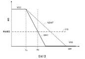
當第一時序信號(例如,時鐘信號CLK)從低轉換為高時,感測放大器110進入感測階段,在感測階段中,輸入電路115感測在輸入電路115的輸入121和123處的差分輸入信號(例如,差分資料信號)。圖3示出了在輸入電壓INP高於輸入電壓INN(這可以表示位元值1)的情況下,在感測階段期間的電壓DINT和NDINT的示例。在所述示例中,第一時序信號(例如,時鐘信號CLK)在時間T1處從低轉換為高。此外,在所述示例中,第一輸入電晶體142和第二輸入電晶體146具有相同的閾值電壓310,這在圖3中被示出。When the first timing signal (for example, the clock signal CLK) transitions from low to high, the
在時間Tl處,第一開關116導通,並且第二開關130和第三開關134關斷。這允許第一輸入電晶體120基於驅動第一輸入電晶體120的輸入電壓INP來下拉第一輸出124處的電壓DINT,並且允許第二輸入電晶體122基於驅動第二輸入電晶體122的輸入電壓INN來下拉第二輸出126處的電壓NDINT。在所述示例中,第一輸出124處的電壓DINT以比第二輸出126處的電壓NDINT快的速率被下拉。這是因為在所述示例中,第一輸入電晶體120由比第二輸入電晶體122高的電壓驅動(即,INP>INN)。At time T1, the
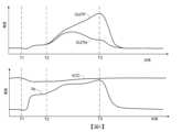
在時間T2處,電壓DINT下降到低於閾值電壓310,這將再生電路140的第二輸入電晶體146關斷。因為電壓NDINT在時間T2處仍然高於閾值電壓,再生電路140的第一輸入電晶體142在時間T2處仍然導通。在時間T2處,再生電路140從感測階段轉換到決策階段,在決策階段中,第二輸入電晶體146的關斷觸發再生電路140的再生反饋,所述再生反饋由反相電路150和160的交叉耦接提供,如上面所討論的。在所述示例中,再生反饋上拉第一輸出170並且下拉第二輸出175。圖4中圖示了這種情況的一個示例,其示出了第一輸出170處的輸出電壓OUTP和第二輸出175處的輸出電壓OUTN的情形。如圖4中所示,再生反饋上拉第一輸出170並且下拉第二輸出175,這在再生電路140的輸出170和175處產生大差分輸出電壓,所述大差分輸出電壓表示解析位元值。在所述示例中,輸出電壓OUTP高於輸出電壓OUTN,這可以表示位元決策為1。At time T2, the voltage DINT drops below the
在時間T3處,第一時序信號從高轉換回低,使得感測放大器110返回到重設階段,並且輸出電壓OUTP和OUTN中的每個輸出電壓返回到大約零伏特(即,地)的重設電壓。就在時間T3之前,耦接到再生電路140的輸出170和175的鎖存器(未示出)可以鎖存所解析的位元值。鎖存器可以包括設定-重設(S-R)鎖存器或另一種類型的鎖存器。At time T3, the first timing signal transitions from high back to low, causing the
上面針對輸入電壓INP高於輸入電壓INN的情況討論了感測階段和決策階段。對於輸入電壓INN高於輸入電壓INP的情況,在感測階段期間,在輸入電路115的第二輸出126處的電壓NDINT在輸入電路115的第一輸出124處的電壓DINT之前下降到低於閾值電壓310,使得第一輸入電晶體142在第二輸入電晶體146之前關斷。當這種情況出現時,感測放大器110從感測階段轉換到決策階段,在決策階段中,第一輸入電晶體142的關斷觸發再生電路140的再生反饋。如上所述,再生反饋由反相電路150和160的交叉耦接提供。在所述情況下,再生反饋上拉第二輸出175並且下拉第一輸出170,產生輸出電壓OUTN高於輸出電壓OUTP的大差分輸出電壓,所述大差分輸出電壓可以表示位元決策為0。The sensing phase and the decision phase are discussed above for the case where the input voltage INP is higher than the input voltage INN. For the case where the input voltage INN is higher than the input voltage INP, during the sensing phase, the voltage NDINT at the
在上述示例中,第一開關116被導通,第二開關130和第三開關134被關斷,並且開關180在感測階段和決策階段期間被導通。當電壓DINT和NDINT中的一個電壓下降到低於輸入電晶體142和146的閾值電壓310時(這會觸發再生電路140的再生反饋以解析位元值(即,做出位元決策)),感測放大器110進入決策階段,如上面所討論的。In the above example, the
當反相電路150和160的第一供電端子156和166透過開關180耦接到供電軌112時,反相電路150和160的交叉耦接提供再生增益。在感測階段期間,反相電路150和160可以透過開關180從供電軌112汲取大電流,使得跨過開關180出現大電流電阻(IR)壓降。大IR壓降減小了在反相電路150和160的第一供電端子156和166處的供電電壓(被標記為“Vp”)。圖4中圖示了這種情況的一個示例,其示出了供電軌112處的供電電壓VCC和供電節點185處的供電電壓Vp的情形,供電節點185耦接到反相電路150和160的第一供電端子156和166。如圖4中所示,在時間T2處的決策階段的開始,由於跨過開關180的IR電壓降,供電節點185處的供電電壓Vp可以比供電軌112處的供電電壓VCC低得多(例如,低30%以上)。較低的供電電壓Vp可能顯著減小由交叉耦接的反相電路150和160提供的再生增益,這顯著減慢了再生電路140可以進行位元決策的速度,並且減小了感測放大器110的靈敏度。The cross-coupling of the
為了解決上述問題,本公開內容的方面提供了一種再生電路,所述再生電路包括耦接在第一輸入電晶體142和第一反相電路150的輸出154之間的第一開關,並且包括耦接在第二輸入電晶體146和第二反相電路160的輸出164之間的第二開關。如下面進一步討論的,第一開關和第二開關透過消除對開關180的需求,並且因此消除由跨過開關180的IR電壓降引起的反相電路150和160的第一供電端子156和166處的供電電壓的減小,從而增加了交叉耦接的反相電路150和160在決策階段期間的再生增益。此外,第一開關位於第二反相電路160的輸入162和第一輸入電晶體142之間的電流路徑之外,並且第二開關位於第一反相電路150的輸入152和第二輸入電晶體146之間的電流路徑之外。如下面進一步討論的,所述特徵顯著減少了在感測階段和決策階段期間流過第一開關和第二開關的電流,這顯著減少了由第一開關和第二開關的存在引起的再生電路140的性能的降級。In order to solve the above problems, aspects of the present disclosure provide a regenerative circuit including a first switch coupled between the
圖5示出了根據本公開內容的某些方面的再生電路140的一個示例。再生電路140可以耦接到圖1中所示的示例性輸入電路115。再生電路140包括上述的第一反相電路150、第二反相電路160、第一輸入電晶體142和第二輸入電晶體146。FIG. 5 illustrates one example of a
第二反相電路160的輸入162耦接到第一輸入電晶體142,並且第一反相電路150的輸入152耦接到第二輸入電晶體146。在某些方面,第二反相電路160的輸入162經由第一金屬佈線530直接耦接到第一輸入電晶體142,並且第一反相電路150的輸入152經由第二金屬佈線535直接耦接到第二輸入電晶體146。第一金屬佈線530和第二金屬佈線535可以均包括晶片上的一個或多個金屬層,以及耦接所述一個或多個金屬層的一個或多個金屬互連結構(例如,通孔)。如本文所使用的,術語“直接耦接”是指兩個設備之間沒有中間設備(例如,開關)的耦接。The
對於利用NFET實現第一輸入電晶體142的示例,第一輸入電晶體142的汲極耦接(例如,經由第一金屬佈線530直接耦接)到第二反相電路160的輸入162,第一輸入電晶體142的閘極耦接到再生電路140的第一輸入144,並且第一輸入電晶體142的源極耦接到地114。對於利用NFET實現第二輸入電晶體146的示例,第二輸入電晶體146的汲極耦接(例如,經由第二金屬佈線535直接耦接)到第一反相電路150的輸入152,第二輸入電晶體146的閘極耦接到再生電路140的第二輸入148,並且第二輸入電晶體146的源極耦接到地114。然而,應當理解,第一輸入電晶體142和第二輸入電晶體146不限於所述示例,並且第一輸入電晶體142和第二輸入電晶體146中的每個電晶體可以利用PFET或另一種類型的電晶體實現。For the example of implementing the
在所述示例中,第一反相電路150的第一供電端子156和第二反相電路160的第一供電端子166耦接到供電軌112。在某些方面,第一反相電路150的第一供電端子156和第二反相電路160的第一供電端子166直接耦接(例如,經由金屬佈線)到供電軌112,其中圖1和圖2中所示的開關180被省略。與圖1和圖2中的再生電路140相比,透過消除由跨過開關180的IR電壓降引起的反相電路150和160的第一供電端子156和166處的供電電壓的減小,直接耦接顯著增加了反相電路150和160的第一供電端子156和166處的供電電壓。第一反相電路150的第二供電端子158和第二反相電路160的第二供電端子168耦接到地114。In the depicted example, the
再生電路140還包括第一開關510和第二開關520。第一開關510耦接在第一輸入電晶體142和第一反相電路150的輸出154之間,並且第二開關520耦接在第二輸入電晶體146和第二反相電路160的輸出164之間。對於輸入電晶體142和146中的每個電晶體利用NFET實現的示例,第一開關510耦接在第一輸入電晶體142的汲極與第一反相電路150的輸出154之間,並且第二開關520耦接在第二輸入電晶體146的汲極與第二反相電路160的輸出164之間。The
在圖5的示例中,第一開關510具有由時序信號(例如,時鐘信號CLK)驅動的控制輸入515,並且第二開關520具有由時序信號驅動的控制輸入525。所述時序信號可以與用於控制圖1中所示的示例性輸入電路115中的開關116、130和134的時序信號相同,或者可以是另一個時序信號。在某些方面,第一開關510和第二開關520被配置成在時序信號處於第一邏輯狀態(例如,低)時關斷,並且在時序信號處於第二邏輯狀態(例如,高)時導通。如下面進一步討論的,時序信號在重設階段期間處於第一邏輯狀態,並且在感測階段和決策階段期間處於第二邏輯狀態。因此,第一開關510和第二開關520在重設階段期間被關斷,並且在感測階段和決策階段期間被導通。In the example of FIG. 5 , the
現在將根據本公開內容的某些方面討論圖5中示出的示例性再生電路140的示例性操作。An example operation of the
當時序信號(例如,時鐘信號CLK)處於第一邏輯狀態(例如,低)時,再生電路140處於重設階段。在重設階段中,時序信號將第一開關510和第二開關520關斷。將第一開關510關斷使第二反相電路160的輸入162與第一反相電路150的輸出154去耦接,這斷開了第二反相電路160的輸入162和第一反相電路150的輸出154之間的再生反饋路徑。將第二開關520關斷使第一反相電路150的輸入152與第二反相電路160的輸出164去耦接,這斷開了第一反相電路150的輸入152和第二反相電路160的輸出164之間的再生反饋路徑。When a timing signal (eg, clock signal CLK) is in a first logic state (eg, low),
透過在重設階段期間斷開再生反饋路徑,第一開關510和第二開關520在重設階段期間停用再生電路140的再生反饋。相比之下,在圖1和圖2中,透過關斷開關180而在重設階段期間停用再生反饋,關斷開關180將反相電路150和160的第一供電端子156和166與供電軌112去耦接,並且因此切斷從供電軌112到反相電路150和160的供電。因此,第一開關510和第二開關520允許時序信號在重設階段期間停用再生電路140的再生反饋,而無需圖1和圖2中的開關180。這消除了對開關180的需求,這允許反相電路150和160的第一供電端子156和166直接耦接到供電軌112。如下面進一步討論的,在重設階段期間,第一開關510和第二開關520也可以禁止電流從供電軌112流到地114。By opening the regenerative feedback path during the reset phase, the
如上所述,在重設階段期間,再生電路140的第一輸入144處的電壓NDINT和再生電路140的第二輸入148處的電壓DINT被輸入電路115上拉至VCC。作為結果,電壓NDINT高於第一輸入電晶體142的閾值電壓,並且電壓DINT高於第二輸入電晶體146的閾值電壓(假設VCC高於第一輸入電晶體142和第二輸入電晶體146中的每個電晶體的閾值電壓)。這使得第一輸入電晶體142導通,並且將第二反相電路160的輸入162下拉到地114,並且使得第二輸入電晶體146導通,並且將第一反相電路150的輸入152下拉到地114。As mentioned above, during the reset phase, the voltage NDINT at the
當時序信號(例如,時鐘信號CLK)從第一邏輯狀態(例如,低)轉換到第二邏輯狀態(例如,高)時,再生電路140進入感測階段,並且時序信號將第一開關510和第二開關520導通。將第一開關510導通使第二反相電路160的輸入162透過第一開關510耦接到第一反相電路150的輸出154,並且將第二開關520導通使第一反相電路150的輸入152透過第二開關520耦接到第二反相電路160的輸出164。作為結果,第一反相電路150和第二反相電路160透過開關510和520交叉耦接。這使再生電路140能夠在感測階段中進行再生反饋。再生反饋允許再生電路140實現再生。When a timing signal (eg, clock signal CLK) transitions from a first logic state (eg, low) to a second logic state (eg, high),
如上所述,反相電路150和160的第一供電端子156和166可以直接耦接到供電軌112,與圖1和圖2中所示的示例(其中跨過開關180的IR電壓降顯著減小了反相電路150和160的第一供電端子156和166處的供電電壓)相比,這顯著增加了反相電路150和160的第一供電端子156和166處的供電電壓。反相電路150和160的第一供電端子156和166處增加的供電電壓增加了再生電路140的再生增益,這增加了再生電路140可以進行位元決策的速度,並且增加了感測放大器110的靈敏度。As mentioned above, the
如上所述,在感測階段期間,根據輸入到輸入電路115的差分信號(例如,差分資料信號)的極性,輸入電路115以不同的速率下拉再生電路140的第一輸入144處的電壓NDINT和下拉再生電路140的第二輸入148處的電壓DINT。當電壓NDINT和DINT中的一個電壓下降到低於第一輸入電晶體142和第二輸入電晶體146的閾值電壓310時(這會觸發再生電路140的再生反饋以做出位元決策),再生電路140從感測階段轉換到決策階段。如上所述,再生反饋由反相電路150和160透過開關510和520(兩者都被導通)的交叉耦接而被致能。再生反饋使得再生電路140將輸出170和175中的一個輸出拉高,並且將輸出170和175中的另一個拉低,以根據電壓NDINT和DINT中的哪一個先下降到低於閾值電壓310來解析位元值,如上面所討論的。As described above, during the sensing phase, the
第一開關510和第二開關520的存在可能潛在地在再生電路140的輸出170和175處引起大電壓偏移,所述大電壓偏移使再生電路140的性能降級並且可能需要被校準掉。大電壓偏移可以由在感測階段和決策階段期間跨過第一開關510的IR電壓降和跨第二開關520的IR電壓降的差異引起,所述差異被再生電路140的再生增益放大。跨過開關510和開關520的IR電壓降的差異可能是由於,例如,第一開關510和第二開關520的失配。由跨過開關510和開關520的IR電壓降的差異引起的電壓偏移可以透過顯著減小跨過開關510和開關520的IR電壓降來被顯著減小,如下面進一步討論的。The presence of the
如圖5中所示,第一開關510位於第二反相電路160的輸入162和第一輸入電晶體142之間的電流路徑之外。這是因為第一開關510耦接在第一輸入電晶體142和第一反相電路150的輸出154之間。作為結果,在感測階段和決策階段期間,在第二反相電路160的輸入162和第一輸入電晶體142之間流動的電流不流過第一開關510,這顯著減小了跨過第一開關510的IR電壓降。As shown in FIG. 5 , the
類似地,第二開關520位於第一反相電路150的輸入152和第二輸入電晶體146之間的電流路徑之外。這是因為第二開關520耦接在第二輸入電晶體146和第二反相電路160的輸出164之間。作為結果,在感測階段和決策階段期間,在第一反相電路150的輸入152和第二輸入電晶體146之間流動的電流不流過第二開關520,這顯著減小了跨過第二開關520的IR電壓降。Similarly, the
因此,將第一開關510定位在第二反相電路160的輸入162和第一輸入電晶體142之間的電流路徑之外,並且將第二開關520定位在第一反相電路150的輸入152和第二輸入電晶體146之間的電流路徑之外,顯著減小了在感測階段和決策階段期間流過第一開關510的電流和流過第二開關520的電流。流過第一開關510和第二開關520的電流減小顯著減小了跨過第一開關510和第二開關520的IR電壓降。跨第一開關510和第二開關520的IR電壓降的顯著減小,顯著減小了IR電壓降對再生電路140的電壓偏移的影響,導致由於IR電壓降的差異引起的電壓偏移明顯更小。Accordingly, the
圖6A示出了一個示例,其中第一開關510利用第一NFET 610實現,並且第二開關520利用第二NFET 620實現。在所述示例中,第一NFET 610的源極和汲極之一耦接到第一輸入電晶體142(例如,第一輸入電晶體142的汲極),第一NFET 610的源極和汲極中的另一個耦接到第一反相電路150的輸出154,並且第一NFET 610的閘極耦接到控制輸入515以接收時序信號(例如,時鐘信號CLK)。第二NFET 620的源極和汲極之一耦接到第二輸入電晶體146(例如,第二輸入電晶體146的汲極),並且第二NFET 620的源極和汲極中的另一個耦接到第二反相電路160的輸出164,並且第二NFET 620的閘極耦接到控制輸入525以接收時序信號(例如,時鐘信號CLK)。FIG. 6A shows an example where the
在所述示例中,第一開關510和第二開關520在時序信號為低時被關斷,並且在時序信號為高時被導通。因此,在所述示例中,再生電路140在時序信號為低時處於重設階段,並且在時序信號為高時處於感測階段和決策階段。In the example, the
應當理解,第一開關510和第二開關520不限於圖6A中所示的示例性實施方式,並且第一開關510和第二開關520中的每個開關可以用另一種類型的電晶體、傳輸閘或另一種類型的開關來實現。例如,圖6B示出了一個示例,其中第一開關510還包括與第一NFET 610並聯耦接的第一PFET 630。在所述示例中,第一NFET 610和第一PFET 630形成傳輸閘(例如,互補式金屬氧化物半導體(CMOS)傳輸閘),其中第一PFET 630的閘極由時序信號的互補(例如,互補時鐘信號CLKb)驅動。此外,在所述示例中,第二開關520還包括與第二NFET 620並聯耦接的第二PFET 640。在所述示例中,第二NFET 620和第二PFET 640形成傳輸閘,其中第二PFET 640的閘極由時序信號的互補(例如,互補時鐘信號CLKb)驅動。在一些實施方式中,可以從開關510和520省略NFET 610和620,其中第一PFET 630耦接在第一輸入電晶體142(例如,第一輸入電晶體142的汲極)與第一反相電路150的輸出154之間,並且第二PFET 640耦接在第二輸入電晶體146(例如,第二輸入電晶體146的汲極)與第二反相電路160的輸出164之間。It should be understood that the
圖7A示出了根據某些方面的第一反相電路150和第二反相電路160的示例性實施方式。在所述示例中,第一反相電路150包括第一開關720和第二開關725。第一開關720耦接在第一反相電路150的輸出154和第二供電端子158之間,並且第二開關725耦接在第一反相電路150的輸出154和第一供電端子156之間。第一開關720的控制輸入722和第二開關725的控制輸入727耦接到第一反相電路150的輸入152。FIG. 7A illustrates an example implementation of a
在操作中,當輸入152處的電壓為高(例如,接近VCC)時,第一開關720被配置成導通,並且第二開關725被配置成關斷。在所述情況下,第一開關720將輸出154拉低。當輸入152處的電壓為低(例如,接近地)時,第一開關720被配置成關斷,並且第二開關725被配置成導通。在所述情況下,第二開關725將輸出154拉高。開關720和開關725中的每個開關可以利用一個或多個電晶體、傳輸閘或另一種類型的開關來實現。In operation, when the voltage at the
在所述示例中,第二反相電路160包括第一開關730和第二開關735。第一開關730耦接在第二反相電路160的輸出164和第二供電端子168之間,並且第二開關735耦接在第二反相電路160的輸出164和第一供電端子166之間。第一開關730的控制輸入732和第二開關735的控制輸入737耦接到第二反相電路160的輸入162。In the example, the
在操作中,當輸入162處的電壓為高(例如,接近VCC)時,第一開關730被配置成導通,並且第二開關735被配置成關斷。在所述情況下,第一開關730將輸出164拉低。當輸入162處的電壓為低(即,接近地)時,第一開關730被配置成關斷,並且第二開關735被配置成導通。在所述情況下,第二開關735將輸出164拉高。開關730和開關735中的每個開關可以利用一個或多個電晶體、傳輸閘或另一種類型的開關來實現。In operation, when the voltage at the
圖7B示出了第一反相電路150中的第一開關720和第二開關725的示例性實施方式。在所述示例中,第一開關720包括NFET 740並且第二開關725包括PFET 745。NFET 740的汲極耦接到輸出154,NFET 740的閘極耦接到控制輸入722,並且NFET 740的源極耦接到第二供電端子158。PFET 745的源極耦接到第一供電端子156,PFET 745的汲極耦接到輸出154,並且PFET 745的閘極耦接到控制輸入727。FIG. 7B shows an exemplary implementation of the
圖7B還示出了第二反相電路160中的第一開關730和第二開關735的示例性實施方式。在所述示例中,第一開關730包括NFET 750並且第二開關735包括PFET 755。NFET 750的汲極耦接到輸出164,NFET 750的閘極耦接到控制輸入732,並且NFET 750的源極耦接到第二供電端子168。PFET 755的源極耦接到第一供電端子166,PFET 755的汲極耦接到輸出164,並且PFET 755的閘極耦接到控制輸入737。FIG. 7B also shows an exemplary implementation of the
在圖7A和圖7B所示的示例中,第一開關510和第二開關520在重設階段期間停用從供電軌112到地114的電流路徑。在圖7C中圖示了這種情況的一個示例,圖7C利用“X”表示再生電路140中在重設階段期間被關斷的設備中的每個設備。如圖7C中所示,第一開關510和第二開關520被關斷。此外,第一反相電路150中的第一開關720(例如,NFET 740)被關斷。這是因為在重設階段期間,第二輸入電晶體146將第一反相電路150的輸入152拉到地114,這將第一開關720關斷。第二反相電路160中的第一開關730(例如,NFET 750)也被關斷。這是因為在重設階段期間,第一輸入電晶體142將第二反相電路160的輸入162拉到地114,這將第一開關730關斷。In the example shown in FIGS. 7A and 7B , the
第一開關510和第一反相電路150中的第一開關720的關斷防止電流從第一反相電路150的第一供電端子156流到地114,並且第二開關520和第二反相電路160中的第一開關730的關斷防止電流從第二反相電路160的第一供電端子166流到地114。作為結果,在重設階段期間,第一開關510和第二開關520禁止電流從供電軌112流到地114,這減小了再生電路140在重設階段期間的功耗。相比之下,在圖1和圖2所示的示例中,在重設階段期間,透過關斷開關180來禁止從供電軌112到地114的電流流動,這將反相電路150和160與供電軌112去耦接。Turning off the
應當理解,反相電路150和160不限於圖7A和圖7B中所示的示例性實施方式。因此,應當理解,反相電路150和160中的每個反相電路可以利用被配置成將邏輯狀態(即,邏輯位準或邏輯值)反相的各種電路中的任何一種來實現,並且因此不限於特定實施方式。It should be understood that the
圖8示出了根據本公開內容的某些方面的一個示例,其中再生電路140還包括第一上拉電晶體810和第二上拉電晶體820。如下面進一步討論的,第一上拉電晶體810和第二上拉電晶體820提升了再生電路140的再生增益。FIG. 8 shows an example according to certain aspects of the present disclosure, wherein the
在圖8的示例中,第一上拉電晶體810利用第一PFET實現,並且第二上拉電晶體820利用第二PFET實現。在所述示例中,第一上拉電晶體810的源極耦接到供電軌112,第一上拉電晶體810的汲極耦接到第一反相電路150的輸入152,並且第一上拉電晶體810的閘極耦接到第一反相電路150的輸出154。第二上拉電晶體820的源極耦接到供電軌112,第二上拉電晶體820的汲極耦接到第二反相電路160的輸入162,並且第二上拉電晶體820的閘極耦接到第二反相電路160的輸出164。In the example of FIG. 8, the first pull-up
當在感測階段期間電壓DINT下降得比電壓NDINT快時(例如,在輸入電路115的輸入121和123處的INP>INN),第二輸入電晶體146在第一輸入電晶體142之前關斷。這觸發再生電路140的再生反饋,以上拉第一輸出170並且下拉第二輸出175。因為第一上拉電晶體810的閘極透過第一開關510耦接到第二輸出175,第二輸出175的下拉將第一上拉電晶體810導通。當第一上拉電晶體810導通時,第一上拉電晶體810將第一反相電路150的輸入152上拉至供電軌112上的供電電壓VCC,這有助於將第一反相電路150的輸出154驅動為低。由於第一反相電路150的輸出154透過第一開關510耦接到第二輸出175,將第一反相電路150的輸出154驅動為低有助於下拉第二輸出175,並且因此提升了再生電路140的再生增益。When voltage DINT falls faster than voltage NDINT during the sensing phase (eg, INP>INN at
當在感測階段期間電壓NDINT下降得比電壓DINT快時(例如,輸入電路115的輸入121和123處的INN>INP),第一輸入電晶體142在第二輸入電晶體146之前關斷。這觸發再生電路140的再生反饋,以上拉第二輸出175並且下拉第一輸出170。因為第二上拉電晶體820的閘極透過第二開關520耦接到第一輸出170,第一輸出170的下拉將第二上拉電晶體820導通。當第二上拉電晶體820導通時,第二上拉電晶體820將第二反相電路160的輸入162上拉至供電軌112上的供電電壓VCC,這有助於將第二反相電路160的輸出164驅動為低。由於第二反相電路160的輸出164透過第二開關520耦接到第一輸出170,因此,將第二反相電路160的輸出164驅動為低有助於下拉第一輸出170,並且因此提升了再生電路140的再生增益。When voltage NDINT falls faster than voltage DINT during the sensing phase (eg, INN>INP at
因此,第一上拉電晶體810和第二上拉電晶體820提升了再生電路140的再生增益。對於在感測階段期間電壓DINT下降得比電壓NDINT快的情況(例如,在輸入電路115的輸入121和123處的INP>INN),第一上拉電晶體810透過將第一反相電路150的輸入152上拉到供電電壓VCC而提升了再生增益。對於在感測階段期間電壓NDINT下降得比電壓DINT快的情況(例如,輸入電路115的輸入121和123處的INN>INP),第二上拉電晶體820透過將第二反相電路160的輸入162上拉至供電電壓VCC而提升了再生增益。Therefore, the first pull-up
圖9示出了根據某些方面的感測放大器110的輸入電路115中的第一開關116、第二開關130和第三開關134的示例性實施方式。注意,為了便於說明,圖9中未示出再生電路140的細節。如圖9中所示,輸入電路115的第一輸出124耦接到再生電路140的第二輸入148,並且輸入電路115的第二輸出126耦接到再生電路140的第一輸入144。再生電路140可以利用圖5至圖8中所示的示例性實施方式中的任一個實現。9 illustrates an example implementation of
在圖9的示例中,第一開關116利用NFET 910實現,其中NFET 910的汲極耦接到輸入電晶體120和122的源極,NFET 910的閘極耦接到控制輸入118,並且NFET 910的源極耦接到地。第二開關130利用第一PFET 915實現,其中第一PFET 915的源極耦接到供電軌112,第一PFET 915的閘極耦接到控制輸入132,並且第一PFET 915的汲極耦接到第一輸入電晶體120的汲極。第三開關134利用第二PFET 920實現,其中第二PFET 920的源極耦接到供電軌112,第二PFET 920的閘極耦接到控制輸入136,並且第二PFET 920的汲極耦接到第二輸入電晶體122的汲極。In the example of FIG. 9,
輸入電路115中的第一開關116、第二開關130和第三開關134可以由與再生電路140中的第一開關510和第二開關520相同的時序信號(例如,時鐘信號CLK)驅動。在所述示例中,當時序信號為低時,第一開關116被關斷,第二開關130和第三開關134被導通。當時序信號為高時,第一開關116被導通,第二開關130和第三開關134被關斷。在所述示例中,時序信號在重設階段期間為低,並且在感測階段和決策階段期間為高。The
圖10示出了可以使用本公開內容的方面的系統1005的示例。在所述示例中,系統1005包括第一晶片1010和第二晶片1015,其中SerDes可以用於第一晶片1010和第二晶片1015之間的通信。第一晶片1010包括串聯器1020、驅動器1030、第一輸出接腳1040和第二輸出接腳1042。第二晶片1015包括第一接收接腳1050、第二接收接腳1052、接收器1060、感測放大器110、鎖存器1070和解串器1080。FIG. 10 illustrates an example of a
在所述示例中,第一晶片1010和第二晶片1015經由包括第一線1044和第二線1046的差分串行鏈路耦接。第一線1044耦接在第一輸出接腳1040和第一接收接腳1050之間,並且第二線1046耦接在第二輸出接腳1042和第二接收接腳1052之間。線1044和1046均可以利用基板(例如,印刷電路板)上的金屬線、導線等實現。In the depicted example,
在第一晶片1010上,串聯器1020被配置成:接收並行資料串流(例如,來自第一晶片1010上的處理器),並且將並行資料串流轉換成串行資料串流,所述串行資料串流在串聯器1020的輸出1025處輸出。驅動器1030具有耦接到串聯器1020的輸出1025的輸入1032、耦接到第一輸出接腳1040的第一輸出1034,以及耦接到第二輸出接腳1042的第二輸出1036。驅動器1030被配置成:接收串行資料串流,將串行資料串流轉換為差分信號,以及利用所述差分資料信號驅動差分串行鏈路的線1044和1046,以將差分信號傳送到第二晶片1015。應當理解,第一晶片1010可以包括圖10中未示出的額外組件(例如,耦接到輸出接腳1040和1042的阻抗匹配網路、耦接在串聯器1020和驅動器1030之間的預驅動器等)。On
在第二晶片1015上,接收器1060具有耦接到第一接收接腳1050的第一輸入1062、耦接到第二接收接腳1052的第二輸入1064、耦接到感測放大器110的第一輸入121的第一輸出1066,以及耦接到感測放大器110的第二輸入123的第二輸出1068。接收器1060可以包括放大器和等化器中的至少一個(例如,以補償第一晶片1010和第二晶片1015之間的頻率相關信號衰減)。如上所述,感測放大器110接收來自接收器1060的差分信號,並且基於差分信號做出位元決策。On the
在圖10的示例中,感測放大器110的第一輸出170耦接到鎖存器1070的第一輸入1072,並且感測放大器110的第二輸出175耦接到鎖存器1070的第二輸入1074。鎖存器1070具有耦接到解串器1080的輸入1082的輸出1076。鎖存器1070被配置成:鎖存來自感測放大器110的位元決策,並且將對應的位輸出到解串器1080。解串器1080被配置成將所述位元轉換為並行資料串流,並行資料串流可以被輸出到第二晶片1015上的一個或多個組件(未示出)以進行進一步處理。應當理解,第二晶片1015可以包括圖10中未示出的額外組件(例如,耦接到接收接腳1050和1052的阻抗匹配網路、時鐘恢復電路等)。In the example of FIG. 10, the
在圖10的示例中,第二晶片1015還包括時序信號電路1090,時序信號電路1090被配置成產生用於感測放大器110的時序信號(例如,時鐘信號CLK),並且在輸出1094處輸出時序信號。輸出1094可以耦接到輸入電路115中的開關116、130和134的控制輸入,並且可以耦接到感測放大器110的再生電路140中的開關510和520的控制輸入。In the example of FIG. 10 , second die 1015 also includes
在某些方面,時序信號電路1090可以基於感測放大器110的位元決策而使用時鐘資料恢復來恢復時序信號(例如,時鐘信號CLK)。時序信號電路1090的輸入1092可以耦接到鎖存器1070的輸出(在圖10的示例中示出),或者可以耦接到感測放大器110的輸出170和175之一或兩者以接收位元決策。In some aspects,
在某些方面,時序信號電路1090可以包括時鐘產生器,所述時鐘產生器可以包括鎖相迴路(PLL)、延遲鎖定迴路(DLL)、振盪器或其任何組合,以產生時序信號(例如,時鐘信號CLK)。應當理解,時序信號電路1090可以使用各種類型的時鐘產生器來實現。In some aspects, the
在圖10的示例中,鎖存器1070的第一輸入1072耦接到第一輸出170,並且因此耦接到第二輸入電晶體146的汲極,並且鎖存器1070的第二輸入1074耦接到第二輸出175並且因此耦接到第一輸入電晶體142的汲極。然而,應當理解,本公開內容不限於所述示例。在另一個示例中,鎖存器1070的第一輸入1072可以耦接到第二反相電路160的輸出164,並且鎖存器1070的第二輸入1074可以耦接到第一反相電路150的輸出154。In the example of FIG. 10, the
圖11圖示了根據某些方面的操作感測放大器的再生電路的方法1100。再生電路(例如,再生電路140)包括:第一反相電路(例如,第一反相電路150),具有輸入(例如,輸入152)和輸出(例如,輸出154);第二反相電路(例如,第二反相電路160),具有輸入(例如,輸入162)和輸出(例如,輸出164);第一電晶體(例如,第一輸入電晶體142),耦接到第二反相電路的輸入;以及第二電晶體(例如,第二輸入電晶體146),耦接到第一反相電路的輸入。11 illustrates a
在方塊1110處,在重設階段中,第一反相電路的輸出與第一電晶體去耦接。例如,第一反相電路的輸出可以透過將第一開關510關斷來與第一電晶體去耦接。At
在方塊1120處,在重設階段中,第二反相電路的輸出與第二電晶體去耦接。例如,第二反相電路的輸出可以透過將第二開關520關斷來與第二電晶體去耦接。At
在方塊1130處,在感測階段中,第一反相電路的輸出耦接到第一電晶體。例如,第一反相電路的輸出可以透過將第一開關510導通來耦接到第一電晶體。At
在方塊1140處,在感測階段中,第二反相電路的輸出耦接到第二電晶體。例如,第二反相電路的輸出可以透過將第二開關520導通來耦接到第二電晶體。At
在某些方面,方法1100還可以包括利用第一輸入信號(例如,電壓NDINT)驅動第一電晶體的閘極,以及利用第二輸入信號(例如,電壓DINT)驅動第二電晶體的閘極。第一輸入信號和第二輸入信號可以由輸入電路115基於輸入到輸入電路115的資料信號(例如,差分資料信號)產生。In some aspects,
在某些方面,在重設階段中,第一輸入信號高於第一電晶體的閾值電壓,並且第二輸入信號高於第二電晶體的閾值電壓。在一個示例中,第一電晶體的閾值電壓可以與第二電晶體的閾值電壓大致相同。In certain aspects, during the reset phase, the first input signal is above the threshold voltage of the first transistor and the second input signal is above the threshold voltage of the second transistor. In one example, the threshold voltage of the first transistor may be approximately the same as the threshold voltage of the second transistor.
在某些方面,在感測階段中,第一輸入信號高於第一電晶體的閾值電壓,並且第二輸入信號高於第二電晶體的閾值電壓。在某些方面,在感測階段中,第一輸入信號(例如,電壓NDINT)以第一速率下降(即,減小),並且第二輸入信號(例如,電壓DINT)以第二速率下降(即,減小),其中第一速率和第二速率不同(例如,基於輸入到輸入電路115的資料信號的極性)。In certain aspects, during the sensing phase, the first input signal is above the threshold voltage of the first transistor and the second input signal is above the threshold voltage of the second transistor. In certain aspects, during the sensing phase, the first input signal (eg, voltage NDINT) ramps down (ie, decreases) at a first rate, and the second input signal (eg, voltage DINT) ramps down at a second rate ( That is, decreases), where the first rate and the second rate are different (eg, based on the polarity of the data signal input to the input circuit 115).
方法1100還可以包括:當第一輸入信號下降到低於第一電晶體的閾值電壓或第二輸入信號下降到低於第二電晶體的閾值電壓時,從感測階段轉換到決策階段。方法1100還可以包括:在決策階段中,基於第一輸入信號和第二輸入信號解析位元值。例如,解析位元值可以包括:如果在第二輸入信號下降到低於第二電晶體的閾值電壓之前,第一輸入信號下降到低於第一電晶體的閾值電壓,則解析到第一位元值,並且如果在第一輸入信號下降到低於第一電晶體的閾值電壓之前,第二輸入信號下降到低於第二電晶體的閾值電壓,則解析到第二位元值。第一位元值可以是1並且第二位元值可以是0,或者反之。在某些方面,在決策階段中,第一反相電路的輸出耦接到第一電晶體,並且第二反相電路的輸出耦接到第二電晶體,第二電晶體將第一反相電路和第二反相電路交叉耦接。這是因為第一電晶體耦接到第二反相電路的輸入,並且第二電晶體耦接到第一反相電路的輸入。第一反相電路和第二反相電路的交叉耦接提供了再生反饋,這有利於解析位元值。The
在以下編號的條款中描述了實施方式示例:Example implementations are described in the following numbered clauses:
1.一種再生電路,包括:1. A regenerative circuit comprising:
第一反相電路,具有輸入和輸出;a first inverting circuit having an input and an output;
第二反相電路,具有輸入和輸出;a second inverting circuit having an input and an output;
第一電晶體,耦接到所述第二反相電路的所述輸入,其中所述第一電晶體的閘極被配置成接收第一輸入信號;a first transistor coupled to the input of the second inverting circuit, wherein a gate of the first transistor is configured to receive a first input signal;
第二電晶體,耦接到所述第一反相電路的所述輸入,其中所述第二電晶體的閘極被配置成接收第二輸入信號;a second transistor coupled to the input of the first inverting circuit, wherein a gate of the second transistor is configured to receive a second input signal;
第一開關,耦接在所述第一電晶體和所述第一反相電路的所述輸出之間,其中所述第一開關的控制輸入被配置成接收時序信號;以及a first switch coupled between the first transistor and the output of the first inverting circuit, wherein a control input of the first switch is configured to receive a timing signal; and
第二開關,耦接在所述第二電晶體和所述第二反相電路的所述輸出之間,其中所述第二開關的控制輸入被配置成接收所述時序信號。A second switch coupled between the second transistor and the output of the second inverter circuit, wherein a control input of the second switch is configured to receive the timing signal.
2.根據條款1所述的再生電路,其中:2. A regenerative circuit as described in clause 1, wherein:
所述第一開關耦接在所述第一電晶體的汲極與所述第一反相電路的所述輸出之間;以及the first switch is coupled between the drain of the first transistor and the output of the first inverter circuit; and
所述第二開關耦接在所述第二電晶體的汲極與所述第二反相電路的所述輸出之間。The second switch is coupled between the drain of the second transistor and the output of the second inverter circuit.
3.根據條款2所述的再生電路,其中:3. A regenerative circuit as described in clause 2, wherein:
所述第一電晶體的源極耦接到地;以及the source of the first transistor is coupled to ground; and
所述第二電晶體的源極耦接到所述地。The source of the second transistor is coupled to the ground.
4.根據條款2或3所述的再生電路,其中所述第一電晶體包括第一n型場效電晶體(NFET)並且所述第二電晶體包括第二NFET。4. The regenerative circuit of clause 2 or 3, wherein the first transistor comprises a first n-type field effect transistor (NFET) and the second transistor comprises a second NFET.
5.根據條款2至4中的任意一項所述的再生電路,其中:5. A regenerative circuit according to any one of clauses 2 to 4, wherein:
所述第一電晶體的所述汲極直接耦接到所述第二反相電路的所述輸入;以及the drain of the first transistor is directly coupled to the input of the second inverting circuit; and
所述第二電晶體的所述汲極直接耦接到所述第一反相電路的所述輸入。The drain of the second transistor is directly coupled to the input of the first inverter circuit.
6.根據條款1至5中的任意一項所述的再生電路,其中:6. A regenerative circuit according to any one of clauses 1 to 5, wherein:
所述第一開關包括第三電晶體,所述第三電晶體具有被配置成接收所述時序信號的閘極;以及the first switch includes a third transistor having a gate configured to receive the timing signal; and
所述第二開關包括第四電晶體,所述第四電晶體具有被配置成接收所述時序信號的閘極。The second switch includes a fourth transistor having a gate configured to receive the timing signal.
7.根據條款6所述的再生電路,其中:7. A regenerative circuit as described in clause 6, wherein:
所述第三電晶體的源極和汲極之一耦接到所述第一電晶體的汲極,並且所述第三電晶體的所述源極和所述汲極中的另一個耦接到所述第一反相電路的所述輸出;以及One of the source and the drain of the third transistor is coupled to the drain of the first transistor, and the other of the source and the drain of the third transistor is coupled to to the output of the first inverting circuit; and
所述第四電晶體的源極和汲極之一耦接到所述第二電晶體的汲極,並且所述第四電晶體的所述源極和所述汲極中的另一個耦接到所述第二反相電路的所述輸出。One of the source and the drain of the fourth transistor is coupled to the drain of the second transistor, and the other of the source and the drain of the fourth transistor is coupled to to the output of the second inverting circuit.
8.根據條款6或7所述的再生電路,其中:8. A regenerative circuit as described in
所述第三電晶體包括第一n型場效電晶體(NFET);以及the third transistor comprises a first n-type field effect transistor (NFET); and
所述第四電晶體包括第二NFET。The fourth transistor includes a second NFET.
9.根據條款1至5中的任意一項所述的再生電路,還包括:9. A regenerative circuit according to any one of clauses 1 to 5, further comprising:
第三電晶體,耦接在所述第一反相電路的所述輸入和供電軌之間;以及a third transistor coupled between the input of the first inverting circuit and a supply rail; and
第四電晶體,耦接在所述第二反相電路的所述輸入和所述供電軌之間。The fourth transistor is coupled between the input of the second inverter circuit and the power supply rail.
10.根據條款9所述的再生電路,其中:10. A regenerative circuit as described in clause 9, wherein:
所述第三電晶體的閘極耦接到所述第一反相電路的所述輸出;以及the gate of the third transistor is coupled to the output of the first inverter circuit; and
所述第四電晶體的閘極耦接到所述第二反相電路的所述輸出。The gate of the fourth transistor is coupled to the output of the second inverter circuit.
11.根據條款9或10所述的再生電路,其中:11. A regenerative circuit as described in clause 9 or 10, wherein:
所述第三電晶體的源極耦接到所述供電軌,並且所述第三電晶體的汲極耦接到所述第一反相電路的所述輸入;以及the source of the third transistor is coupled to the supply rail, and the drain of the third transistor is coupled to the input of the first inverting circuit; and
所述第四電晶體的源極耦接到所述供電軌,並且所述第四電晶體的汲極耦接到所述第二反相電路的所述輸入。The source of the fourth transistor is coupled to the power supply rail, and the drain of the fourth transistor is coupled to the input of the second inverting circuit.
12.根據條款9至11中的任意一項所述的再生電路,其中:12. A regenerative circuit according to any one of clauses 9 to 11, wherein:
所述第三電晶體包括第一p型場效電晶體(PFET);以及the third transistor comprises a first p-type field effect transistor (PFET); and
所述第四電晶體包括第二PFET。The fourth transistor includes a second PFET.
13.根據條款1至12中的任意一項所述的再生電路,其中所述時序信號包括時鐘信號。13. A regeneration circuit according to any one of clauses 1 to 12, wherein the timing signal comprises a clock signal.
14.根據條款1至13中的任意一項所述的再生電路,其中所述第一開關的所述控制輸入和所述第二開關的所述控制輸入耦接到被配置成產生所述時序信號的時序信號電路。14. A regenerative circuit according to any one of clauses 1 to 13, wherein the control input of the first switch and the control input of the second switch are coupled to a circuit configured to generate the timing signal timing signal circuit.
15.一種感測放大器,包括:15. A sense amplifier comprising:
輸入電路,其中所述輸入電路包括:an input circuit, wherein the input circuit includes:
第一電晶體,其中所述第一電晶體的閘極被配置成接收第一輸入信號,並且所述第一電晶體的汲極耦接到所述輸入電路的第一輸出;以及a first transistor, wherein a gate of the first transistor is configured to receive a first input signal, and a drain of the first transistor is coupled to a first output of the input circuit; and
第二電晶體,其中所述第二電晶體的閘極被配置成接收第二輸入信號,並且所述第二電晶體的汲極耦接到所述輸入電路的第二輸出;以及a second transistor, wherein the gate of the second transistor is configured to receive a second input signal, and the drain of the second transistor is coupled to a second output of the input circuit; and
再生電路,其中所述再生電路包括:a regenerative circuit, wherein the regenerative circuit includes:
第一反相電路,具有輸入和輸出;a first inverting circuit having an input and an output;
第二反相電路,具有輸入和輸出;a second inverting circuit having an input and an output;
第三電晶體,耦接到所述第二反相電路的所述輸入,其中所述第三電晶體的閘極耦接到所述輸入電路的所述第二輸出;a third transistor coupled to the input of the second inverting circuit, wherein a gate of the third transistor is coupled to the second output of the input circuit;
第四電晶體,耦接到所述第一反相電路的所述輸入,其中所述第四電晶體的閘極耦接所述輸入電路的所述第一輸出;a fourth transistor coupled to the input of the first inverter circuit, wherein a gate of the fourth transistor is coupled to the first output of the input circuit;
第一開關,耦接在所述第三電晶體和所述第一反相電路的所述輸出之間,其中所述第一開關的控制輸入被配置成接收時序信號;以及a first switch coupled between the third transistor and the output of the first inverting circuit, wherein a control input of the first switch is configured to receive a timing signal; and
第二開關,耦接在所述第四電晶體和所述第二反相電路的所述輸出之間,其中所述第二開關的控制輸入被配置成接收所述時序信號。A second switch coupled between the fourth transistor and the output of the second inverter circuit, wherein a control input of the second switch is configured to receive the timing signal.
16.根據條款15所述的感測放大器,其中所述輸入電路還包括:16. The sense amplifier of clause 15, wherein the input circuit further comprises:
第三開關,耦接在所述第一電晶體的所述汲極和供電軌之間;以及a third switch coupled between the drain of the first transistor and a supply rail; and
第四開關,耦接在所述第二電晶體的所述汲極和所述供電軌之間。The fourth switch is coupled between the drain of the second transistor and the power supply rail.
17.根據條款16所述的感測放大器,其中:17. The sense amplifier of clause 16, wherein:
所述第三開關的控制輸入被配置成接收所述時序信號;以及a control input of the third switch configured to receive the timing signal; and
所述第四開關的控制輸入被配置成接收所述時序信號。The control input of the fourth switch is configured to receive the timing signal.
18.根據條款16或17所述的感測放大器,其中所述輸入電路還包括第五開關,所述第五開關耦接在所述第一電晶體的源極和地之間,並且耦接在所述第二電晶體的源極和所述地之間。18. A sense amplifier according to clause 16 or 17, wherein the input circuit further comprises a fifth switch coupled between the source of the first transistor and ground, and coupled between the between the source of the second transistor and the ground.
19.根據條款18所述的感測放大器,其中:19. The sense amplifier of clause 18, wherein:
所述第三開關的控制輸入被配置成接收所述時序信號;a control input of the third switch configured to receive the timing signal;
所述第四開關的控制輸入被配置成接收所述時序信號;以及a control input of the fourth switch configured to receive the timing signal; and
所述第五開關的控制輸入被配置成接收所述時序信號。A control input of the fifth switch is configured to receive the timing signal.
20.根據條款15至19中的任意一項所述的感測放大器,其中:20. A sense amplifier according to any one of clauses 15 to 19, wherein:
所述第一開關耦接在所述第三電晶體的汲極與所述第一反相電路的所述輸出之間;以及the first switch is coupled between the drain of the third transistor and the output of the first inverter circuit; and
所述第二開關耦接在所述第四電晶體的汲極與所述第二反相電路的所述輸出之間。The second switch is coupled between the drain of the fourth transistor and the output of the second inverter circuit.
21.根據條款20所述的感測放大器,其中:twenty one. The sense amplifier of clause 20, wherein:
所述第三電晶體的源極耦接到地;以及the source of the third transistor is coupled to ground; and
所述第四電晶體的源極耦接到所述地。The source of the fourth transistor is coupled to the ground.
22.根據條款20或21所述的感測放大器,其中:twenty two. A sense amplifier according to clause 20 or 21, wherein:
所述第三電晶體的所述汲極直接耦接到所述第二反相電路的所述輸入;以及the drain of the third transistor is directly coupled to the input of the second inverting circuit; and
所述第四電晶體的所述汲極直接耦接到所述第一反相電路的所述輸入。The drain of the fourth transistor is directly coupled to the input of the first inverter circuit.
23.根據條款15至22中的任意一項所述的感測放大器,其中:twenty three. A sense amplifier according to any one of clauses 15 to 22, wherein:
所述第一開關包括第五電晶體,所述第五電晶體具有被配置成接收所述時序信號的閘極;以及the first switch includes a fifth transistor having a gate configured to receive the timing signal; and
所述第二開關包括第六電晶體,所述第六電晶體具有被配置成接收所述時序信號的閘極。The second switch includes a sixth transistor having a gate configured to receive the timing signal.
24.根據條款23所述的再生電路,其中:twenty four. A regenerative circuit according to clause 23, wherein:
所述第五電晶體的源極和汲極之一耦接到所述第三電晶體的汲極,並且所述第五電晶體的所述源極和所述汲極中的另一個耦接到所述第一反相電路的所述輸出;以及One of the source and the drain of the fifth transistor is coupled to the drain of the third transistor, and the other of the source and the drain of the fifth transistor is coupled to to the output of the first inverting circuit; and
所述第六電晶體的源極和汲極之一耦接到所述第四電晶體的汲極,並且所述第六電晶體的所述源極和所述汲極中的另一個耦接到所述第二反相電路的所述輸出。One of the source and the drain of the sixth transistor is coupled to the drain of the fourth transistor, and the other of the source and the drain of the sixth transistor is coupled to to the output of the second inverting circuit.
25.一種操作感測放大器的再生電路的方法,其中所述再生電路包括具有輸入和輸出的第一反相電路、具有輸入和輸出的第二反相電路、耦接到所述第二反相電路的所述輸入的第一電晶體,以及耦接到所述第一反相電路的所述輸入的第二電晶體,所述方法包括:25. A method of operating a regenerative circuit of a sense amplifier, wherein the regenerative circuit includes a first inverting circuit having an input and an output, a second inverting circuit having an input and an output, a A first transistor of the input, and a second transistor coupled to the input of the first inverting circuit, the method comprising:
在重設階段中,During the reset phase,
將所述第一反相電路的所述輸出與所述第一電晶體去耦接;以及decoupling the output of the first inverting circuit from the first transistor; and
將所述第二反相電路的所述輸出與所述第二電晶體去耦接;以及decoupling the output of the second inverting circuit from the second transistor; and
在感測階段中,During the sensing phase,
將所述第一反相電路的所述輸出耦接到所述第一電晶體;以及coupling the output of the first inverting circuit to the first transistor; and
將所述第二反相電路的所述輸出耦接到所述第二電晶體。The output of the second inverting circuit is coupled to the second transistor.
26.根據條款25所述的方法,還包括:26. The method described in clause 25, further comprising:
利用第一輸入信號驅動所述第一電晶體的閘極;以及driving the gate of the first transistor with a first input signal; and
利用第二輸入信號驅動所述第二電晶體的閘極。The gate of the second transistor is driven by a second input signal.
27.根據條款26所述的方法,其中:27. A method according to clause 26, wherein:
在所述重設階段中,所述第一輸入信號高於所述第一電晶體的閾值電壓,並且所述第二輸入信號高於所述第二電晶體的閾值電壓。In the reset phase, the first input signal is higher than the threshold voltage of the first transistor, and the second input signal is higher than the threshold voltage of the second transistor.
28.根據條款27所述的方法,其中:28. A method according to clause 27, wherein:
在所述感測階段中,所述第一輸入信號高於所述第一電晶體的所述閾值電壓,並且所述第二輸入信號高於所述第二電晶體的所述閾值電壓。In the sensing phase, the first input signal is higher than the threshold voltage of the first transistor, and the second input signal is higher than the threshold voltage of the second transistor.
29.根據條款28所述的方法,其中:29. A method according to clause 28, wherein:
在所述感測階段中,所述第一輸入信號以第一速率下降,所述第二輸入信號以第二速率下降,並且所述第一速率和所述第二速率不同。During the sensing phase, the first input signal falls at a first rate, the second input signal falls at a second rate, and the first rate and the second rate are different.
30.根據條款29所述的方法,還包括:30. The method described in clause 29, further comprising:
當所述第一輸入信號下降到低於所述第一電晶體的所述閾值電壓或所述第二輸入信號下降到低於所述第二電晶體的所述閾值電壓時,從所述感測階段轉換到決策階段。When the first input signal falls below the threshold voltage of the first transistor or the second input signal falls below the threshold voltage of the second transistor, from the sense transition from the testing stage to the decision-making stage.
31.根據條款30所述的方法,還包括:31. The method described in clause 30, further comprising:
在所述決策階段中,基於所述第一輸入信號和所述第二輸入信號解析位元值。In the decision phase, bit values are resolved based on the first input signal and the second input signal.
32.根據條款25至31中的任意一項所述的方法,其中所述再生電路包括耦接在所述第一反相電路的所述輸出和所述第一電晶體之間的第一開關,並且包括耦接在所述第二反相電路的所述輸出和所述第二電晶體之間的第二開關,並且其中:32. A method according to any one of clauses 25 to 31, wherein said regenerative circuit comprises a first switch coupled between said output of said first inverting circuit and said first transistor, and including a second switch coupled between the output of the second inverting circuit and the second transistor, and wherein:
將所述第一反相電路的所述輸出與所述第一電晶體去耦接包括將所述第一開關關斷;decoupling the output of the first inverter circuit from the first transistor includes turning off the first switch;
將所述第二反相電路的所述輸出與所述第二電晶體去耦接包括將所述第二開關關斷;decoupling the output of the second inverting circuit from the second transistor includes turning off the second switch;
將所述第一反相電路的所述輸出耦接到所述第一電晶體包括將所述第一開關導通;以及coupling the output of the first inverting circuit to the first transistor includes turning on the first switch; and
將所述第二反相電路的所述輸出耦接到所述第二電晶體包括將所述第二開關導通。Coupling the output of the second inverting circuit to the second transistor includes turning on the second switch.
33.根據條款25至32中的任意一項所述的方法,其中所述第一電晶體的汲極直接耦接到所述第二反相電路的所述輸入,並且所述第二電晶體的汲極直接耦接到所述第一反相電路的所述輸入。33. The method of any one of clauses 25 to 32, wherein the drain of the first transistor is directly coupled to the input of the second inverting circuit, and the drain of the second transistor pole is directly coupled to the input of the first inverting circuit.
34.根據條款33所述的方法,其中:34. A method according to clause 33, wherein:
將所述第一反相電路的所述輸出與所述第一電晶體去耦接包括:將所述第一反相電路的所述輸出與所述第一電晶體的所述汲極去耦接;Decoupling the output of the first inverter circuit from the first transistor includes: decoupling the output of the first inverter circuit from the drain of the first transistor catch;
將所述第二反相電路的所述輸出與所述第二電晶體去耦接包括:將所述第二反相電路的所述輸出與所述第二電晶體的所述汲極去耦接;Decoupling the output of the second inverting circuit from the second transistor includes: decoupling the output of the second inverting circuit from the drain of the second transistor catch;
將所述第一反相電路的所述輸出耦接到所述第一電晶體包括:將所述第一反相電路的所述輸出耦接到所述第一電晶體的所述汲極;以及Coupling the output of the first inverting circuit to the first transistor includes: coupling the output of the first inverting circuit to the drain of the first transistor; as well as
將所述第二反相電路的所述輸出耦接到所述第二電晶體包括:將所述第二反相電路的所述輸出耦接到所述第二電晶體的所述汲極。Coupling the output of the second inverting circuit to the second transistor includes coupling the output of the second inverting circuit to the drain of the second transistor.
35.根據條款34所述的方法,其中所述再生電路包括耦接在所述第一反相電路的所述輸出與所述第一電晶體的所述汲極之間的第一開關,並且包括耦接在所述第二反相電路的所述輸出與所述第二電晶體的所述汲極之間的第二開關,並且其中:35. The method of clause 34, wherein the regenerative circuit includes a first switch coupled between the output of the first inverting circuit and the drain of the first transistor, and includes a coupling a second switch connected between the output of the second inverting circuit and the drain of the second transistor, and wherein:
將所述第一反相電路的所述輸出與所述第一電晶體的所述汲極去耦接包括將所述第一開關關斷;decoupling the output of the first inverter circuit from the drain of the first transistor includes turning off the first switch;
將所述第二反相電路的所述輸出與所述第二電晶體的所述汲極去耦接包括將所述第二開關關斷;decoupling the output of the second inverting circuit from the drain of the second transistor includes turning off the second switch;
將所述第一反相電路的所述輸出耦接到所述第一電晶體的所述汲極包括將所述第一開關導通;以及coupling the output of the first inverting circuit to the drain of the first transistor includes turning on the first switch; and
將所述第二反相電路的所述輸出耦接到所述第二電晶體的所述汲極包括將所述第二開關導通。Coupling the output of the second inverting circuit to the drain of the second transistor includes turning on the second switch.
36.一種系統,包括:36. A system comprising:
感測放大器,包括:Sense amplifiers, including:
輸入電路,其中所述輸入電路包括:an input circuit, wherein the input circuit includes:
第一電晶體,其中所述第一電晶體的閘極被配置成接收第一輸入信號,並且所述第一電晶體的汲極耦接到所述輸入電路的第一輸出;以及a first transistor, wherein a gate of the first transistor is configured to receive a first input signal, and a drain of the first transistor is coupled to a first output of the input circuit; and
第二電晶體,其中所述第二電晶體的閘極被配置成接收第二輸入信號,並且所述第二電晶體的汲極耦接到所述輸入電路的第二輸出;以及a second transistor, wherein the gate of the second transistor is configured to receive a second input signal, and the drain of the second transistor is coupled to a second output of the input circuit; and
再生電路,其中所述再生電路包括:a regenerative circuit, wherein the regenerative circuit includes:
第一反相電路,具有輸入和輸出;a first inverting circuit having an input and an output;
第二反相電路,具有輸入和輸出;a second inverting circuit having an input and an output;
第三電晶體,耦接到所述第二反相電路的所述輸入,其中所述第三電晶體的閘極耦接到所述輸入電路的所述第二輸出;a third transistor coupled to the input of the second inverting circuit, wherein a gate of the third transistor is coupled to the second output of the input circuit;
第四電晶體,耦接到所述第一反相電路的所述輸入,其中所述第四電晶體的閘極耦接到所述輸入電路的所述第一輸出;a fourth transistor coupled to the input of the first inverting circuit, wherein a gate of the fourth transistor is coupled to the first output of the input circuit;
第一開關,耦接在所述第三電晶體和所述第一反相電路的所述輸出之間,其中所述第一開關的控制輸入被配置成接收時序信號;以及a first switch coupled between the third transistor and the output of the first inverting circuit, wherein a control input of the first switch is configured to receive a timing signal; and
第二開關,耦接在所述第四電晶體和所述第二反相電路的所述輸出之間,其中所述第二開關的控制輸入被配置成接收所述時序信號;a second switch coupled between the fourth transistor and the output of the second inverting circuit, wherein a control input of the second switch is configured to receive the timing signal;
鎖存器,具有輸入和輸出,其中所述鎖存器的所述輸入耦接到所述感測放大器;以及a latch having an input and an output, wherein the input of the latch is coupled to the sense amplifier; and
解串器,具有耦接到所述鎖存器的所述輸出的輸入。a deserializer having an input coupled to the output of the latch.
37.根據條款36所述的系統,還包括:37. The system of clause 36, further comprising:
串聯器,具有輸出;a serializer having an output;
驅動器,具有輸入和輸出,其中所述驅動器的所述輸入耦接到所述串聯器的所述輸出;以及a driver having an input and an output, wherein the input of the driver is coupled to the output of the serializer; and
接收器,具有輸入和輸出,其中所述接收器的所述輸入耦接到所述驅動器的所述輸出,並且所述接收器的輸出耦接到所述感測放大器。a receiver having an input and an output, wherein the input of the receiver is coupled to the output of the driver and the output of the receiver is coupled to the sense amplifier.
38.根據條款37所述的系統,其中所述接收器的所述輸出包括:38. The system of clause 37, wherein said output of said receiver comprises:
第一輸出,耦接到所述第一電晶體的所述閘極;以及a first output coupled to the gate of the first transistor; and
第二輸出,耦接到所述第二電晶體的所述閘極。The second output is coupled to the gate of the second transistor.
39.根據條款36至條款38中的任意一項所述的系統,其中所述鎖存器的所述輸入包括:39. The system of any one of clauses 36 to 38, wherein said input to said latch comprises:
第一輸入,耦接到所述第四電晶體的汲極或所述第二反相電路的所述輸出;以及a first input coupled to the drain of the fourth transistor or the output of the second inverting circuit; and
第二輸入,耦接到所述第三電晶體的汲極或所述第一反相電路的所述輸出。The second input is coupled to the drain of the third transistor or the output of the first inverter circuit.
應當理解,本公開內容不限於上面用於描述本公開內容的方面的示例性術語。例如,輸入電路115也可以被稱為感測電路或另一術語。再生電路140也可以被稱為決策電路、交叉耦接鎖存器或另一術語。反相電路也可以被稱為反相器、反相電路或另一術語。邏輯狀態也可以被稱為邏輯位準、邏輯值或另一術語。It should be understood that the disclosure is not limited to the exemplary terminology used above to describe aspects of the disclosure. For example, the
在本文中使用諸如“第一”、“第二”等名稱對元素的任何引用通常不限制這些元素的數量或順序。相反,這些名稱在本文中用作區分兩個以上元素或元素的多個實例的方便方式。因此,對第一和第二元素的引用並不意味著只能採用兩個元素,或者第一元素必須在第二元素之前。Any reference to elements herein using designations such as "first," "second," etc. generally does not limit the quantity or order of those elements. Rather, these names are used herein as a convenient way of distinguishing between two or more elements or instances of an element. Therefore, references to first and second elements do not imply that only two elements can be used, or that the first element must precede the second element.
在本公開內容內,“示例性”一詞用於意指“用作示例、實例或說明”。在本文中描述為“示例性”的任何實施方式或方面不必被解釋為比本公開內容的其他方面更優選或有利。同樣地,術語“方面”不要求本公開內容的所有方面都包括所討論的特徵、優點或操作模式。如本文關於說明值或性質而使用的術語“大約”旨在表示在陳述值或性質的10%以內。In this disclosure, the word "exemplary" is used to mean "serving as an example, instance, or illustration." Any implementation or aspect described herein as "exemplary" is not necessarily to be construed as preferred or advantageous over other aspects of the disclosure. Likewise, the term "aspects" does not require that all aspects of the disclosure include the discussed feature, advantage or mode of operation. As used herein with respect to a stated value or property, the term "about" is intended to mean within 10% of the stated value or property.
提供本公開內容的前述描述以使本領域的任何技術人員能夠製作或使用本公開內容。對於本領域技術人員來說,對本公開內容的各種修改將是明顯的,並且在不脫離本公開內容的精神或範圍的情況下,本文定義的一般原理可以被應用於其他變型。因此,本公開內容不旨在限於本文描述的示例,而是要被賦予與本文公開的原理和新穎特徵一致的最寬範圍。The preceding description of the disclosure is provided to enable any person skilled in the art to make or use the disclosure. Various modifications to the disclosure will be readily apparent to those skilled in the art, and the generic principles defined herein may be applied to other modifications without departing from the spirit or scope of the disclosure. Thus, the present disclosure is not intended to be limited to the examples described herein but is to be accorded the widest scope consistent with the principles and novel features disclosed herein.
110:感測放大器 112:供電軌 114:地 115:輸入電路 116:第一開關 117:節點 118:控制輸入 121:第一輸入 122:第二輸入電晶體 123:第二輸入 124:第一輸出 126:第二輸出 130:第二開關 132:控制輸入 134:第三開關 136:控制輸入 140:再生電路 142:第一輸入電晶體 144:第一輸入 146:第二輸入電晶體 148:第二輸入 150:第一反相電路 152:輸入 154:輸出 156:第一供電端子 158:第二供電端子 160:第二反相電路 162:輸入 164:輸出 166:第一供電端子 168:第二供電端子 170:第一輸出 175:第二輸出 180:開關 182:控制輸入 185:供電節點 210:PFET 310:閾值電壓 510:第一開關 515:控制輸入 520:第二開關 525:控制輸入 530:第一金屬佈線 535:第二金屬佈線 610:第一NFET 620:第二NFET 630:第一PFET 640:第二PFET 720:第一開關 722:控制輸入 725:第二開關 727:控制輸入 730:第一開關 732:控制輸入 735:第二開關 737:控制輸入 740:NFET 745:PFET 750:NFET 755:PFET 810:第一上拉電晶體 820:第二上拉電晶體 910:NFET 915:第一PFET 920:第二PFET 1005:系統 1010:第一晶片 1015:第二晶片 1020:串聯器 1025:輸出 1030:驅動器 1032:輸入 1034:第一輸出 1036:第二輸出 1040:第一輸出接腳 1042:第二輸出接腳 1044:第一線 1046:第二線 1050:第一接收接腳 1052:第二接收接腳 1060:接收器 1062:第一輸入 1064:第二輸入 1066:第一輸出 1068:第二輸出 1070:鎖存器 1072:第一輸入 1074:第二輸入 1076:輸出 1080:解串器 1082:輸入 1090:時序信號電路 1092:輸入 1094:輸出 1100:方法 1110:方塊 1120:方塊 1130:方塊 1140:方塊 VSS:接地電壓 VCC:供電電壓 INP:第一輸入電壓 INN:第二輸入電壓 OUTP:輸出電壓 OUTN:輸出電壓 NDINT:電壓 DINT:電壓 CLK:時鐘信號 CLKb:互補時鐘信號 Vp:供電電壓 T1:時間 T2:時間 T3:時間110: sense amplifier 112: Power supply rail 114: ground 115: input circuit 116: first switch 117: node 118: Control input 121: first input 122: Second input transistor 123: second input 124: first output 126: second output 130: second switch 132: Control input 134: The third switch 136: Control input 140: Regenerative circuit 142: The first input transistor 144: first input 146: Second input transistor 148: second input 150: The first inverting circuit 152: input 154: output 156: the first power supply terminal 158: the second power supply terminal 160: the second inverting circuit 162: input 164: output 166: the first power supply terminal 168: Second power supply terminal 170: first output 175: second output 180: switch 182: Control input 185: Power supply node 210:PFET 310: threshold voltage 510: first switch 515: Control input 520: second switch 525: Control input 530: First metal wiring 535: Second metal wiring 610: First NFET 620: Second NFET 630: First PFET 640: Second PFET 720: first switch 722: Control input 725: second switch 727: Control input 730: first switch 732: Control input 735: second switch 737: Control input 740: NFET 745:PFET 750: NFET 755:PFET 810: The first pull-up transistor 820: Second pull-up transistor 910:NFET 915: First PFET 920: Second PFET 1005: system 1010: first chip 1015: second chip 1020: serializer 1025: output 1030: drive 1032: input 1034: first output 1036: second output 1040: The first output pin 1042: Second output pin 1044: first line 1046: second line 1050: The first receiving pin 1052: The second receiving pin 1060: Receiver 1062: first input 1064: second input 1066: first output 1068: second output 1070:Latch 1072: first input 1074: second input 1076: output 1080: deserializer 1082: Input 1090: Timing signal circuit 1092: Input 1094: output 1100: method 1110: block 1120: block 1130: block 1140: block VSS: ground voltage VCC: supply voltage INP: first input voltage INN: second input voltage OUTP: output voltage OUTN: output voltage NDINT: Voltage DINT: Voltage CLK: clock signal CLKb: Complementary clock signal Vp: supply voltage T1: time T2: time T3: time
圖1示出了根據本公開內容的某些方面的包括輸入電路和再生電路的感測放大器的示例。1 illustrates an example of a sense amplifier including an input circuit and a regeneration circuit, in accordance with certain aspects of the present disclosure.
圖2示出了根據本公開內容的某些方面的再生電路中的開關的示例性實施方式。FIG. 2 illustrates an example implementation of a switch in a regeneration circuit according to certain aspects of the present disclosure.
圖3是根據本公開內容的某些方面的時序圖,其示出了由輸入電路輸出到再生電路的電壓的示例。3 is a timing diagram illustrating an example of voltage output by an input circuit to a regeneration circuit, in accordance with certain aspects of the present disclosure.
圖4是根據本公開內容的某些方面的時序圖,其示出了再生電路的輸出電壓在感測階段和決策階段期間的示例。4 is a timing diagram illustrating an example of an output voltage of a regenerative circuit during a sensing phase and a decision phase, in accordance with certain aspects of the present disclosure.
圖5示出了根據本公開內容的某些方面的再生電路的示例。5 illustrates an example of a regeneration circuit in accordance with certain aspects of the present disclosure.
圖6A示出了根據本公開內容的某些方面的再生電路中的開關的示例性實施方式。6A illustrates an example implementation of a switch in a regeneration circuit according to certain aspects of the present disclosure.
圖6B示出了根據本公開內容的某些方面的再生電路中的開關的另一示例性實施方式。6B illustrates another example implementation of a switch in a regeneration circuit in accordance with certain aspects of the present disclosure.
圖7A示出了根據本公開內容的某些方面的再生電路中的反相電路的示例性實施方式。7A illustrates an example implementation of an inverting circuit in a regenerative circuit according to certain aspects of the present disclosure.
圖7B示出了根據本公開內容的某些方面的反相電路中的開關的示例性實施方式。7B illustrates an example implementation of switches in an inverting circuit in accordance with certain aspects of the present disclosure.
圖7C表示根據本公開內容的某些方面的在重設階段期間在再生電路中被關閉的設備。FIG. 7C illustrates a device that is turned off in a regeneration circuit during a reset phase, according to certain aspects of the present disclosure.
圖8示出了根據本公開內容的某些方面的包括上拉電晶體的再生電路的示例。8 illustrates an example of a regeneration circuit including a pull-up transistor, in accordance with certain aspects of the present disclosure.
圖9示出了根據本公開內容的某些方面的輸入電路中的開關的示例性實施方式。9 illustrates an example implementation of a switch in an input circuit in accordance with certain aspects of the present disclosure.
圖10示出了根據本公開內容的某些方面的可以在其中使用本公開內容的方面的系統的示例。10 illustrates an example of a system in which aspects of the present disclosure may be used in accordance with certain aspects of the present disclosure.
圖11是圖示根據本公開內容的某些方面的用於操作感測放大器的再生電路的示例性方法的流程圖。11 is a flowchart illustrating an example method for operating a regenerative circuit of a sense amplifier in accordance with certain aspects of the present disclosure.
112:供電軌112: Power supply rail
114:地114: ground
140:再生電路140: Regenerative circuit
142:第一輸入電晶體142: The first input transistor
144:第一輸入144: first input
146:第二輸入電晶體146: Second input transistor
148:第二輸入148: second input
150:第一反相電路150: The first inverting circuit
152:輸入152: input
154:輸出154: output
156:第一供電端子156: the first power supply terminal
158:第二供電端子158: the second power supply terminal
160:第二反相電路160: the second inverting circuit
162:輸入162: input
164:輸出164: output
166:第一供電端子166: the first power supply terminal
168:第二供電端子168: Second power supply terminal
170:第一輸出170: first output
175:第二輸出175: second output
510:第一開關510: first switch
515:控制輸入515: Control input
520:第二開關520: second switch
525:控制輸入525: Control input
530:第一金屬佈線530: First metal wiring
535:第二金屬佈線535: Second metal wiring
VSS:接地電壓VSS: ground voltage
VCC:供電電壓VCC: supply voltage
OUTP:輸出電壓OUTP: output voltage
OUTN:輸出電壓OUTN: output voltage
NDINT:電壓NDINT: Voltage
DINT:電壓DINT: Voltage
CLK:時鐘信號CLK: clock signal
Claims (35)
Translated fromChineseApplications Claiming Priority (2)
| Application Number | Priority Date | Filing Date | Title |
|---|---|---|---|
| US17/321,005US11374560B1 (en) | 2021-05-14 | 2021-05-14 | Dynamic cross-coupled regeneration for high-speed sense amplifier |
| US17/321,005 | 2021-05-14 |
Publications (1)
| Publication Number | Publication Date |
|---|---|
| TW202304137Atrue TW202304137A (en) | 2023-01-16 |
Family
ID=81655005
Family Applications (1)
| Application Number | Title | Priority Date | Filing Date |
|---|---|---|---|
| TW111116285ATW202304137A (en) | 2021-05-14 | 2022-04-28 | Dynamic cross-coupled regeneration for high-speed sense amplifier |
Country Status (7)
| Country | Link |
|---|---|
| US (1) | US11374560B1 (en) |
| EP (1) | EP4338158B9 (en) |
| KR (1) | KR102618435B1 (en) |
| CN (1) | CN117378008A (en) |
| BR (1) | BR112023023040A2 (en) |
| TW (1) | TW202304137A (en) |
| WO (1) | WO2022240591A1 (en) |
Families Citing this family (1)
| Publication number | Priority date | Publication date | Assignee | Title |
|---|---|---|---|---|
| US11711077B1 (en)* | 2022-06-02 | 2023-07-25 | Qualcomm Incorporated | High-speed sampler |
Family Cites Families (19)
| Publication number | Priority date | Publication date | Assignee | Title |
|---|---|---|---|---|
| US5508648A (en)* | 1994-08-01 | 1996-04-16 | Intel Corporation | Differential latch circuit |
| US6396308B1 (en) | 2001-02-27 | 2002-05-28 | Sun Microsystems, Inc. | Sense amplifier with dual linearly weighted inputs and offset voltage correction |
| KR100394573B1 (en) | 2001-05-31 | 2003-08-14 | 삼성전자주식회사 | Sense amplifier in semiconductor memory device |
| US7227798B2 (en) | 2002-10-07 | 2007-06-05 | Stmicroelectronics Pvt. Ltd. | Latch-type sense amplifier |
| US7196550B1 (en)* | 2003-06-26 | 2007-03-27 | Cypress Semiconductor Corporation | Complementary CMOS driver circuit with de-skew control |
| EP1777818B1 (en)* | 2004-08-10 | 2010-04-07 | Nippon Telegraph and Telephone Corporation | Master-slave flip-flop, trigger flip-flop and counter |
| JP4467445B2 (en)* | 2005-02-10 | 2010-05-26 | Okiセミコンダクタ株式会社 | Comparator circuit |
| US7388772B1 (en)* | 2006-03-20 | 2008-06-17 | Altera Corporation | Latch circuit |
| US7679405B2 (en)* | 2007-10-24 | 2010-03-16 | Agere Systems Inc. | Latch-based sense amplifier |
| KR101063872B1 (en) | 2009-05-07 | 2011-09-15 | 포항공과대학교 산학협력단 | Low Power Low-Frequency Noise Comparator Circuit for Analog-to-Digital Converters |
| US8604838B2 (en)* | 2011-12-12 | 2013-12-10 | Texas Instruments Incorporated | Comparator with improved time constant |
| US8624632B2 (en) | 2012-03-29 | 2014-01-07 | International Business Machines Corporation | Sense amplifier-type latch circuits with static bias current for enhanced operating frequency |
| US9467133B2 (en)* | 2015-02-27 | 2016-10-11 | Huawei Technologies Co., Ltd. | Comparator apparatus and method |
| US10230361B2 (en)* | 2015-08-28 | 2019-03-12 | Perceptia Devices Australia Pty Ltd | High-speed clocked comparators |
| JP2017112537A (en)* | 2015-12-17 | 2017-06-22 | シナプティクス・ジャパン合同会社 | Inverter circuit |
| KR102319827B1 (en) | 2017-06-28 | 2021-11-01 | 에스케이하이닉스 주식회사 | Amplifier circuit |
| KR102643532B1 (en)* | 2018-08-28 | 2024-03-06 | 에스케이하이닉스 주식회사 | Bitline sense amplifier circuit |
| EP3672077B1 (en) | 2018-12-19 | 2022-07-27 | Socionext Inc. | Comparator circuitry |
| US11095273B1 (en)* | 2020-07-27 | 2021-08-17 | Qualcomm Incorporated | High-speed sense amplifier with a dynamically cross-coupled regeneration stage |
- 2021
- 2021-05-14USUS17/321,005patent/US11374560B1/enactiveActive
- 2022
- 2022-04-28KRKR1020237038338Apatent/KR102618435B1/enactiveActive
- 2022-04-28EPEP22723917.5Apatent/EP4338158B9/enactiveActive
- 2022-04-28BRBR112023023040Apatent/BR112023023040A2/enunknown
- 2022-04-28TWTW111116285Apatent/TW202304137A/enunknown
- 2022-04-28WOPCT/US2022/026719patent/WO2022240591A1/ennot_activeCeased
- 2022-04-28CNCN202280032104.3Apatent/CN117378008A/enactivePending
Also Published As
| Publication number | Publication date |
|---|---|
| KR102618435B1 (en) | 2023-12-27 |
| EP4338158B9 (en) | 2025-08-06 |
| BR112023023040A2 (en) | 2024-01-23 |
| WO2022240591A1 (en) | 2022-11-17 |
| KR20230160405A (en) | 2023-11-23 |
| EP4338158B1 (en) | 2025-03-19 |
| US11374560B1 (en) | 2022-06-28 |
| EP4338158C0 (en) | 2025-03-19 |
| EP4338158A1 (en) | 2024-03-20 |
| CN117378008A (en) | 2024-01-09 |
Similar Documents
| Publication | Publication Date | Title |
|---|---|---|
| US7777521B2 (en) | Method and circuitry to translate a differential logic signal to a CMOS logic signal | |
| TWI768977B (en) | High-speed sense amplifier with a dynamically cross-coupled regeneration stage | |
| US7176720B1 (en) | Low duty cycle distortion differential to CMOS translator | |
| US11295789B2 (en) | Latching sense amplifier | |
| US7388406B2 (en) | CML circuit devices having improved headroom | |
| JP2000207887A (en) | Latch type sense amplifier | |
| US6320422B1 (en) | Complementary source coupled logic | |
| US7629814B2 (en) | Latch circuit and deserializer circuit | |
| US6441649B1 (en) | Rail-to-rail input clocked amplifier | |
| TW202304137A (en) | Dynamic cross-coupled regeneration for high-speed sense amplifier | |
| US12009811B2 (en) | High-speed sampler | |
| US6967505B2 (en) | Input circuit | |
| US20020196064A1 (en) | Edge triggered latch with symmetrical paths from clock to data outputs | |
| JP2025157269A (en) | High-Speed Sampler | |
| BR112023000474B1 (en) | REGENERATION STAGE OF A DETECTION AMPLIFIER AND METHOD OF OPERATION OF A REGENERATION STAGE OF A DETECTION AMPLIFIER | |
| CN117155344A (en) | Dynamic latch circuits, high-speed interface circuits and electronic devices | |
| JP2001217686A (en) | Flip-flop circuit |