TW202249545A - Glass substrates and method for building conductive through-hole vias in glass substrates - Google Patents
Glass substrates and method for building conductive through-hole vias in glass substratesDownload PDFInfo
- Publication number
- TW202249545A TW202249545ATW111121238ATW111121238ATW202249545ATW 202249545 ATW202249545 ATW 202249545ATW 111121238 ATW111121238 ATW 111121238ATW 111121238 ATW111121238 ATW 111121238ATW 202249545 ATW202249545 ATW 202249545A
- Authority
- TW
- Taiwan
- Prior art keywords
- circuit
- coating
- glass substrate
- conductor
- conductive
- Prior art date
Links
- 239000011521glassSubstances0.000titleclaimsabstractdescription71
- 238000000034methodMethods0.000titleclaimsabstractdescription71
- 239000000758substrateSubstances0.000titleclaimsabstractdescription68
- 238000000576coating methodMethods0.000claimsabstractdescription65
- 239000011248coating agentSubstances0.000claimsabstractdescription57
- 238000001039wet etchingMethods0.000claimsabstractdescription6
- 239000004020conductorSubstances0.000claimsdescription33
- KRHYYFGTRYWZRS-UHFFFAOYSA-NFluoraneChemical compoundFKRHYYFGTRYWZRS-UHFFFAOYSA-N0.000claimsdescription8
- 239000011159matrix materialSubstances0.000claimsdescription7
- 238000007650screen-printingMethods0.000claimsdescription7
- 229910000679solderInorganic materials0.000claimsdescription7
- 239000004593EpoxySubstances0.000claimsdescription6
- 239000002253acidSubstances0.000claimsdescription6
- 229910052751metalInorganic materials0.000claimsdescription5
- 239000002184metalSubstances0.000claimsdescription5
- 229920002120photoresistant polymerPolymers0.000claimsdescription4
- 238000007772electroless platingMethods0.000claimsdescription3
- 238000009713electroplatingMethods0.000claimsdescription3
- AMGQUBHHOARCQH-UHFFFAOYSA-Nindium;oxotinChemical compound[In].[Sn]=OAMGQUBHHOARCQH-UHFFFAOYSA-N0.000claimsdescription3
- 238000001259photo etchingMethods0.000claimsdescription3
- 238000007747platingMethods0.000claimsdescription2
- 238000005553drillingMethods0.000claims1
- 230000005855radiationEffects0.000abstractdescription2
- 230000001939inductive effectEffects0.000abstract1
- 239000011241protective layerSubstances0.000description11
- 238000005530etchingMethods0.000description8
- 239000000463materialSubstances0.000description8
- 239000011253protective coatingSubstances0.000description8
- 239000010408filmSubstances0.000description7
- 239000000945fillerSubstances0.000description6
- 238000000206photolithographyMethods0.000description5
- 239000010410layerSubstances0.000description4
- 239000010409thin filmSubstances0.000description3
- 239000004642PolyimideSubstances0.000description2
- BQCADISMDOOEFD-UHFFFAOYSA-NSilverChemical compound[Ag]BQCADISMDOOEFD-UHFFFAOYSA-N0.000description2
- 230000015572biosynthetic processEffects0.000description2
- 238000004519manufacturing processMethods0.000description2
- 229910021420polycrystalline siliconInorganic materials0.000description2
- 229920001721polyimidePolymers0.000description2
- 238000007639printingMethods0.000description2
- 229910052709silverInorganic materials0.000description2
- 239000004332silverSubstances0.000description2
- RYGMFSIKBFXOCR-UHFFFAOYSA-NCopperChemical compound[Cu]RYGMFSIKBFXOCR-UHFFFAOYSA-N0.000description1
- ATJFFYVFTNAWJD-UHFFFAOYSA-NTinChemical compound[Sn]ATJFFYVFTNAWJD-UHFFFAOYSA-N0.000description1
- 229910021417amorphous siliconInorganic materials0.000description1
- 239000011247coating layerSubstances0.000description1
- 238000011109contaminationMethods0.000description1
- 229910052802copperInorganic materials0.000description1
- 239000010949copperSubstances0.000description1
- 230000008021depositionEffects0.000description1
- 238000010586diagramMethods0.000description1
- 238000004806packaging method and processMethods0.000description1
- 230000000149penetrating effectEffects0.000description1
- 229920005591polysiliconPolymers0.000description1
- 239000004065semiconductorSubstances0.000description1
- 239000007787solidSubstances0.000description1
- 239000002344surface layerSubstances0.000description1
Images


Classifications
- H—ELECTRICITY
- H01—ELECTRIC ELEMENTS
- H01L—SEMICONDUCTOR DEVICES NOT COVERED BY CLASS H10
- H01L21/00—Processes or apparatus adapted for the manufacture or treatment of semiconductor or solid state devices or of parts thereof
- H01L21/02—Manufacture or treatment of semiconductor devices or of parts thereof
- H01L21/04—Manufacture or treatment of semiconductor devices or of parts thereof the devices having potential barriers, e.g. a PN junction, depletion layer or carrier concentration layer
- H01L21/18—Manufacture or treatment of semiconductor devices or of parts thereof the devices having potential barriers, e.g. a PN junction, depletion layer or carrier concentration layer the devices having semiconductor bodies comprising elements of Group IV of the Periodic Table or AIIIBV compounds with or without impurities, e.g. doping materials
- H01L21/30—Treatment of semiconductor bodies using processes or apparatus not provided for in groups H01L21/20 - H01L21/26
- H01L21/31—Treatment of semiconductor bodies using processes or apparatus not provided for in groups H01L21/20 - H01L21/26 to form insulating layers thereon, e.g. for masking or by using photolithographic techniques; After treatment of these layers; Selection of materials for these layers
- H01L21/3105—After-treatment
- H01L21/311—Etching the insulating layers by chemical or physical means
- H01L21/31105—Etching inorganic layers
- H01L21/31111—Etching inorganic layers by chemical means
- H—ELECTRICITY
- H01—ELECTRIC ELEMENTS
- H01L—SEMICONDUCTOR DEVICES NOT COVERED BY CLASS H10
- H01L21/00—Processes or apparatus adapted for the manufacture or treatment of semiconductor or solid state devices or of parts thereof
- H01L21/02—Manufacture or treatment of semiconductor devices or of parts thereof
- H01L21/04—Manufacture or treatment of semiconductor devices or of parts thereof the devices having potential barriers, e.g. a PN junction, depletion layer or carrier concentration layer
- H01L21/48—Manufacture or treatment of parts, e.g. containers, prior to assembly of the devices, using processes not provided for in a single one of the groups H01L21/18 - H01L21/326 or H10D48/04 - H10D48/07
- H01L21/4814—Conductive parts
- H01L21/4846—Leads on or in insulating or insulated substrates, e.g. metallisation
- H01L21/486—Via connections through the substrate with or without pins
- H—ELECTRICITY
- H01—ELECTRIC ELEMENTS
- H01L—SEMICONDUCTOR DEVICES NOT COVERED BY CLASS H10
- H01L21/00—Processes or apparatus adapted for the manufacture or treatment of semiconductor or solid state devices or of parts thereof
- H01L21/02—Manufacture or treatment of semiconductor devices or of parts thereof
- H01L21/027—Making masks on semiconductor bodies for further photolithographic processing not provided for in group H01L21/18 or H01L21/34
- H01L21/0271—Making masks on semiconductor bodies for further photolithographic processing not provided for in group H01L21/18 or H01L21/34 comprising organic layers
- H01L21/0273—Making masks on semiconductor bodies for further photolithographic processing not provided for in group H01L21/18 or H01L21/34 comprising organic layers characterised by the treatment of photoresist layers
- H01L21/0274—Photolithographic processes
- H01L21/0275—Photolithographic processes using lasers
- H—ELECTRICITY
- H01—ELECTRIC ELEMENTS
- H01L—SEMICONDUCTOR DEVICES NOT COVERED BY CLASS H10
- H01L23/00—Details of semiconductor or other solid state devices
- H01L23/12—Mountings, e.g. non-detachable insulating substrates
- H01L23/14—Mountings, e.g. non-detachable insulating substrates characterised by the material or its electrical properties
- H01L23/15—Ceramic or glass substrates
- H—ELECTRICITY
- H01—ELECTRIC ELEMENTS
- H01L—SEMICONDUCTOR DEVICES NOT COVERED BY CLASS H10
- H01L23/00—Details of semiconductor or other solid state devices
- H01L23/48—Arrangements for conducting electric current to or from the solid state body in operation, e.g. leads, terminal arrangements ; Selection of materials therefor
- H01L23/481—Internal lead connections, e.g. via connections, feedthrough structures
- H—ELECTRICITY
- H01—ELECTRIC ELEMENTS
- H01L—SEMICONDUCTOR DEVICES NOT COVERED BY CLASS H10
- H01L23/00—Details of semiconductor or other solid state devices
- H01L23/48—Arrangements for conducting electric current to or from the solid state body in operation, e.g. leads, terminal arrangements ; Selection of materials therefor
- H01L23/488—Arrangements for conducting electric current to or from the solid state body in operation, e.g. leads, terminal arrangements ; Selection of materials therefor consisting of soldered or bonded constructions
- H01L23/498—Leads, i.e. metallisations or lead-frames on insulating substrates, e.g. chip carriers
- H01L23/49827—Via connections through the substrates, e.g. pins going through the substrate, coaxial cables
Landscapes
- Engineering & Computer Science (AREA)
- Physics & Mathematics (AREA)
- Condensed Matter Physics & Semiconductors (AREA)
- General Physics & Mathematics (AREA)
- Computer Hardware Design (AREA)
- Microelectronics & Electronic Packaging (AREA)
- Power Engineering (AREA)
- Manufacturing & Machinery (AREA)
- Ceramic Engineering (AREA)
- Chemical & Material Sciences (AREA)
- Optics & Photonics (AREA)
- General Chemical & Material Sciences (AREA)
- Inorganic Chemistry (AREA)
- Chemical Kinetics & Catalysis (AREA)
- Printing Elements For Providing Electric Connections Between Printed Circuits (AREA)
- Manufacturing Of Printed Circuit Boards (AREA)
Abstract
Description
Translated fromChinese本發明是關於一種通孔結構,特別是關於一種但不限定於貫穿玻璃基板的導電通孔。The present invention relates to a through-hole structure, in particular to but not limited to a conductive through-hole penetrating through a glass substrate.
於玻璃基板上預製通孔(設置電路之前)可能造成玻璃碎裂或污染用於製作過程中的工具。舉例來說,具有貫穿通孔(Through-Hole Via,THV)的玻璃可能具有殘餘的應力,這可能導致在製程步驟或步驟之間的機械轉移過程中玻璃破裂;在導體材料中用來填入貫穿通孔的金屬可能在多晶矽(低溫多晶矽(Low Temperature Polycrystal Silicon,LTPS))或非晶矽薄膜電晶體(TFT)這些材料沉積期間作為汙染源。Prefabricating vias on glass substrates (before circuitry is placed) may cause the glass to break or contaminate the tools used in the fabrication process. For example, glass with a Through-Hole Via (THV) may have residual stresses that may cause the glass to break during process steps or mechanical transfer between steps; used in conductor materials to fill Metal through vias may act as a contamination source during deposition of materials such as polysilicon (Low Temperature Polycrystalline Silicon (LTPS)) or amorphous silicon thin film transistor (TFT).
一種於玻璃基板內形成導電貫穿通孔(through-hole-via)的方法,包含:佈置一電路在玻璃基板的一第一表面,使得玻璃基板的第一表面上一區被曝露;塗布一塗層在第一表面以覆蓋電路及第一表面之曝露區,其中該塗層可為一薄膜;移除曝露區上的塗層;利用雷射引起至少一部份的曝露區結構損傷;以及,濕式蝕刻掉至少一部份的曝露區,以形成一通孔。A method of forming a conductive through-hole-via in a glass substrate, comprising: arranging a circuit on a first surface of the glass substrate so that a region on the first surface of the glass substrate is exposed; coating a coating layering on the first surface to cover the circuitry and exposed areas of the first surface, wherein the coating may be a thin film; removing the coating on the exposed areas; causing structural damage to at least a portion of the exposed areas using a laser; and, Wet etching away at least a portion of the exposed area to form a via hole.
為了減少在玻璃基板中的製造問題,一示範實施例在電路已被佈置於玻璃基板上之後形成貫穿通孔(through-hole-via,THV)或導電貫穿通孔。To reduce manufacturing issues in glass substrates, an exemplary embodiment forms through-hole-vias (THVs) or conductive through-vias after the circuitry has been placed on the glass substrate.
圖1描繪根據一實施例中一種於玻璃基板內建立導電貫穿通孔的方法100。在步驟102中,設計電路佈線與指定的貫穿通孔或導電貫穿通孔(THV)位置在玻璃基板上。在步驟104中,施加保護層/塗層在電路上,此保護層/塗層亦可為一薄膜。在步驟106中,在指定的THV位置上方一開口在保護層/塗層內及由保護層/塗層封住的電路上形成。THV位置被設計來在THV形成過程期間避免對薄膜電晶體電路有任何影響。舉例來說,THV位置上方可以不具電路且與其保持安全距離。THV形成過程可能有熱產生而影響到電路表現。於步驟108,在基板內的THV位置形成。於步驟110,形成THV內的導電材料。於步驟112,通過THV及指定電路接點,THV及電路與導電材料電性連接。FIG. 1 depicts a
基板可用來在其電路上形成LED或OLED (例如主動矩陣),以及形成驅動電路及/或軟性電路板(flexible printed circuits,FPCs)於基板的背面用於一顯示模組。基板也可以用作玻璃轉接板並供3D封裝,其中半導體晶片等多種裝置可以同時安裝在基板的頂部及底部,並經由THV電性連接。The substrate can be used to form LEDs or OLEDs (such as active matrix) on its circuit, and to form driving circuits and/or flexible printed circuits (FPCs) on the backside of the substrate for a display module. The substrate can also be used as a glass interposer for 3D packaging, in which multiple devices such as semiconductor chips can be mounted on the top and bottom of the substrate at the same time and electrically connected via THV.
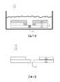
圖2A-圖2E為根據一實施例中於玻璃基板內建立導電貫穿通孔的方法200。於圖2A中,保護層/塗層230塗布在電路220及玻璃基板210上方。塗層230可以是一光阻薄膜而利用光蝕刻方法來圖案化或可以是一抗酸薄膜而通過雷射鑽孔(laser drill holes)於薄膜上圖案化。接著,如圖2B所示,在指定的THV位置10上於塗層230內打開開口。這可以利用光蝕刻或雷射束照射來完成。然後,如圖2C所示,塗層230開口被雷射L照射(例如藉由雷射誘導深度蝕刻(laser induced deep etching,簡稱LIDE))而在指定的THV位置引起玻璃基板210的結構損傷。於圖2D中,損傷的玻璃區域20於蝕刻溶液S(可以例如是氫氟酸基底)中被濕式蝕刻掉。塗層230可抵抗蝕刻溶液S,使得未損傷的玻璃區域的蝕刻速率大幅慢於損傷的玻璃區域20。最後,如圖2E,塗層230被移除且指定的THV位置10形成了通孔10’,具有通孔10’的玻璃基板210準備進入如圖4中所示及描述的導體材料填入程序。2A-2E illustrate a
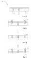
圖3A-圖3E為根據一實施例中於玻璃基板內建立導電貫穿通孔的方法300。在本實施例中,電路320位於一玻璃基板310的第一側及相對的第二側。如圖3A所示,保護層/塗層330同時塗佈於兩側的電路320及玻璃基板310上。塗層330可以是一光阻薄膜而利用光蝕刻方法來圖案化或可以是一抗酸薄膜而通過雷射鑽孔(laser drill holes)於薄膜上圖案化。如圖3B所示,在指定的THV位置10上於兩側的塗層330內打開開口。這可以利用光蝕刻或雷射束照射來完成。接著,如圖3C所示,雷射L照射在塗層330開口上方且在指定的THV位置引起玻璃基板310的結構損傷(例如LIDE)。然後,於圖2D中,損傷的玻璃區域30於蝕刻溶液S(可以是氫氟酸基底)中被濕式蝕刻掉。塗層330可抵抗蝕刻溶液S,使得未損傷的玻璃區域的蝕刻速率大幅慢於損傷的玻璃區域30。最後,如圖3E,塗層330被移除且指定的THV位置10形成了通孔10’,具有通孔10’的玻璃基板310準備進入例如圖4等所示的導體材料填入程序。3A-3E illustrate a
圖4A-圖4D為根據一實施例中於玻璃基板內添加一導體在導電貫穿通孔的方法400。接續前述方法200,於圖4A中,塗佈一填充止檔(filler stop)430於電路420側上方的所有通孔10’。填充止檔430可以是固體層的一暫時層,例如聚醯亞胺(polyimide,簡稱PI)。接著,如圖4B所示,在真空中導電漿料/墨液440填入通孔10’中。填入方法可以例如是網版印刷(screen printing)或注入印刷(inject printing)等。真空可防止空氣進入通孔10’中,進而預防填充止檔430材料跑進通孔10’。選擇性地如圖4C所示,多餘的導電漿料/墨液440的形狀及量難以控制。可能需要移除多餘的部分,並利用明確定義的焊料網版印刷製程以建立明確定義至電路420的連線。因此,固化導電漿料/墨液440之後,可以移除由基板410擠出的多餘導電漿料/墨液440。如圖4D所示,移除填充止檔430。焊料(例如錫膏)經網版印刷並回流焊接以將填滿的THV 10電性連接至電路(例如供顯示器用的主動矩陣或被動矩陣等TFT電路)。4A-4D illustrate a
導電漿料/墨液440材料可以是環氧基銅或銀漿料,或是例如錫、銀的焊料。當採用環氧基材料,導電漿料/墨液440通常需要經過烘烤來固化。若採用焊料,導電漿料/墨液440通常需要經過一高溫回流(攝氏200-400度)以形成接點。The conductive paste/
圖5A-圖5D為根據一實施例中於玻璃基板內添加一導體在導電貫穿通孔的方法500。接續前述方法200,如圖5A所示,塗佈一填充止檔(filler stop)530於玻璃基板510的一側,以及設置一光罩550於另一側的電路52 0上方且其開口550’大於通孔10’,以曝露需要連接到THV的電路接觸點P。如圖5B所示,利用真空網印將導電漿料/墨液540覆蓋曝露的電路接觸點P。接著,如圖5C及圖5D所示,導電漿料/墨液540固化且移除光罩550之後。注意到光罩550上的漿料540可能如圖5C斷裂,或是如圖5D可能在基板510表面層斷裂。5A-5D illustrate a
圖6A-圖6D為根據一實施例中於玻璃基板內添加一導體在導電貫穿通孔的方法600。接續前述方法300,如圖6A所示,形成保護層630於具有通孔10’及電路620的玻璃基板610的兩側。接著,如圖6B所示,於THV區域上方形成開口640以曝露部分的電路620以供連接。如圖6C所示,形成導電塗層650來電性連接玻璃基板610兩側的電路620。如圖6D所示,移除保護層630。導電塗層650材料可以是金屬、氧化銦錫(ITO)或導電漿料/墨液。金屬的導電塗層650可以通過電鍍或化學鍍(electroless plating)形成。導電漿料/油墨的導電塗層650可以通過網印塗佈,使得THV 10可以完全被填入或部分填入。6A-6D illustrate a
鑑於前述揭露內容,以下闡述了各種實施例。應該注意的是,一實施例的一或多個特徵可單獨或組合起來,皆應是在本發明申請案中的申請專利範圍內所考慮的。In light of the foregoing disclosure, various embodiments are set forth below. It should be noted that one or more features of an embodiment may be considered alone or in combination, and all of them shall be considered within the patent scope of the application for the present invention.
實施例1:一種於玻璃基板內形成導電貫穿通孔(through-hole-via)的方法,包含:佈置電路在玻璃基板的一第一表面,使得玻璃基板的第一表面上一區被曝露;塗布一塗層在第一表面以覆蓋電路及第一表面之曝露區,其中塗層可為一保護層或一薄膜;移除曝露區上的塗層;利用雷射(laser radiation)引起至少一部份的曝露區結構損傷;以及,濕式蝕刻掉該至少一部份的曝露區,以形成一通孔。Embodiment 1: A method for forming a conductive through-hole-via in a glass substrate, comprising: arranging a circuit on a first surface of the glass substrate, so that a region on the first surface of the glass substrate is exposed; Coating a coating on the first surface to cover the exposed area of the circuit and the first surface, wherein the coating can be a protective layer or a film; removing the coating on the exposed area; using laser (laser radiation) to cause at least one A portion of the exposed area is structurally damaged; and, wet etching away at least a portion of the exposed area to form a through hole.
實施例2:如實施例1的方法,其中移除曝露區上的塗層是利用光蝕刻(photolithography)或雷射束照射(laser beam irradiation)來實現。Embodiment 2: The method of Embodiment 1, wherein removing the coating on the exposed area is achieved by photolithography or laser beam irradiation.
實施例3:如前述任何實施例的方法,更包含:佈置一第二電路在玻璃基板的一第二表面,使得玻璃基板的第二表面上一第二區被曝露,第一表面相對於第二表面;以及,塗布至第二表面以覆蓋第二電路及第二表面之第二曝露區。Embodiment 3: The method of any of the preceding embodiments, further comprising: arranging a second circuit on a second surface of the glass substrate, so that a second region on the second surface of the glass substrate is exposed, and the first surface is opposite to the first surface. two surfaces; and, coated onto the second surface to cover the second circuit and the second exposed area of the second surface.
實施例4:如前述任何實施例的方法,更包含:在第一表面上放置一填充止檔(filler stop);在一真空中,以一導體填入通孔;以及固化導體。Embodiment 4: The method of any preceding embodiment, further comprising: placing a filler stop on the first surface; filling the via hole with a conductor in a vacuum; and curing the conductor.
實施例5:如前述任何實施例的方法,更包含:塗布一第二塗層至第一表面及第二表面;在通孔中形成開口以曝露第一及第二電路的一部分以連接;形成導電塗層以電性連接第一及第二電路。Embodiment 5: The method of any of the preceding embodiments, further comprising: applying a second coating to the first surface and the second surface; forming an opening in the via hole to expose a portion of the first and second circuits for connection; forming The conductive coating is used to electrically connect the first and second circuits.
實施例6:如前述任何實施例的方法,其中導電塗層包含一金屬鍍層,且形成導電塗層的方法包括電鍍或化學鍍。Embodiment 6: The method of any preceding embodiment, wherein the conductive coating comprises a metal plating, and the method of forming the conductive coating comprises electroplating or electroless plating.
實施例7:如前述任何實施例的方法,其中導電塗層包含氧化銦錫。Embodiment 7: The method of any preceding embodiment, wherein the conductive coating comprises indium tin oxide.
實施例8:如前述任何實施例的方法,其中導電塗層包含一環氧基漿料,且形成導電塗層的方法包括真空網印。Embodiment 8: The method of any preceding embodiment, wherein the conductive coating comprises an epoxy-based paste, and the method of forming the conductive coating comprises vacuum screen printing.
實施例9:如前述任何實施例的方法,更包括:在第一表面上放置一填充止檔(filler stop);在一真空中,以一導體填入通孔; 固化導體;移除填充止檔;以及將通孔內固化的導體電性連接第一電路。Embodiment 9: The method of any preceding embodiment, further comprising: placing a filler stop on the first surface; filling the via hole with a conductor in a vacuum; curing the conductor; removing the filler stop file; and electrically connecting the solidified conductor in the through hole to the first circuit.
實施例10:如前述任何實施例的方法,更包括移除延伸在玻璃基板外多餘的導體。Embodiment 10: The method of any preceding embodiment, further comprising removing excess conductors extending beyond the glass substrate.
實施例11:如前述任何實施例的方法,其中導體包含一環氧基漿料。Embodiment 11: The method of any preceding embodiment, wherein the conductor comprises an epoxy-based paste.
實施例12:如前述任何實施例的方法,其中導體包含一焊料漿。Embodiment 12: The method of any preceding embodiment, wherein the conductor comprises a solder paste.
實施例13:如前述任何實施例的方法,其中塗布塗層包含通過光蝕刻來塗布光阻。Embodiment 13: The method of any preceding embodiment, wherein applying the coating comprises applying photoresist by photoetching.
實施例14:如前述任何實施例的方法,其中塗布塗層包含通過雷射鑽孔(laser drill holes)來圖案化塗布一抗酸薄膜。Embodiment 14: The method of any preceding embodiment, wherein applying the coating comprises pattern coating an acid-resistant film by laser drill holes.
實施例15:如前述任何實施例的方法,其中濕式蝕刻使用氫氟酸且塗層可抗酸。Embodiment 15: The method of any preceding Embodiment, wherein the wet etching uses hydrofluoric acid and the coating is acid resistant.
實施例16:如前述任何實施例的方法,其中電路包含主動矩陣顯示電路。Embodiment 16: The method of any preceding Embodiment, wherein the circuit comprises an active matrix display circuit.
實施例17:如前述任何實施例的方法,其中電路包含被動矩陣顯示電路。Embodiment 17: The method of any preceding Embodiment, wherein the circuit comprises a passive matrix display circuit.
實施例18:如前述任何實施例的方法,更包括:在相對於玻璃基板之第一表面的一第二表面上放置一填充止檔(filler stop);於電路上施加一光罩留下光罩之一曝露區,其寬度大於通孔之寬度;在一真空中,以一導體填入通孔;於電路之曝露的電路接觸點上真空網印導體;固化導體;以及,移除填充止檔。Embodiment 18: The method of any preceding embodiment, further comprising: placing a filler stop on a second surface opposite to the first surface of the glass substrate; applying a photomask over the circuit to leave the light an exposed area of the mask having a width greater than the width of the through hole; filling the through hole with a conductor in a vacuum; vacuum screen printing the conductor on the exposed circuit contacts of the circuit; curing the conductor; and removing the fill stop files.
實施例19:如前述任何實施例的方法,更包含移除任何剩餘的塗層。Embodiment 19: The method of any preceding embodiment, further comprising removing any remaining coating.
實施例20:一種玻璃基板,包含:位於一第一表面上的一第一電路及位於一第二表面上的一第二電路,其中第二表面相對於第一表面;至少一導電貫穿通孔電性連接第一電路及第二電路;其中在第一電路及第二電路形成在玻璃基板上之後,至少一導電貫穿通孔是根據前述任一個實施例來製作。Embodiment 20: A glass substrate, comprising: a first circuit located on a first surface and a second circuit located on a second surface, wherein the second surface is opposite to the first surface; at least one conductive through-hole Electrically connecting the first circuit and the second circuit; wherein after the first circuit and the second circuit are formed on the glass substrate, at least one conductive through-hole is fabricated according to any one of the foregoing embodiments.
10:THV(位置) 10’:通孔 20、30:損傷的玻璃區域 100、200、300、400、500、600:方法 102、104、106、108、110、112:步驟 210:玻璃基板 220:電路 230:保護層/塗層 310:玻璃基板 320:電路 330:保護層/塗層 410:玻璃基板 420:電路 430:填充止檔 440:導電漿料/墨液 510:玻璃基板 520:電路 530:填充止檔 540:導電漿料/墨液 550:光罩 550’:開口 610:玻璃基板 620:電路 630:保護層 640:開口 650:導電塗層 L:雷射 P:接觸點 S:蝕刻溶液10: THV (position) 10': through
為了簡化識別對任何特定元件或流程的說明,請參考以下圖式說明。For ease of identifying descriptions for any particular component or process, reference is made to the following figure descriptions.
圖1為根據本發明一實施例中一種於玻璃基板內建立導電貫穿通孔的方法。FIG. 1 is a diagram illustrating a method for creating conductive through-holes in a glass substrate according to an embodiment of the invention.
圖2A-圖2E為根據一實施例中於玻璃基板內建立導電貫穿通孔的方法。2A-2E illustrate a method for creating conductive through-holes in a glass substrate according to an embodiment.
圖3A-圖3E為根據一實施例中於玻璃基板內建立導電貫穿通孔的方法。3A-3E illustrate a method for creating conductive through-holes in a glass substrate according to an embodiment.
圖4A-圖4D為根據一實施例中於玻璃基板內添加一導體在導電貫穿通孔的方法。4A-4D illustrate a method for adding a conductor in a conductive through-hole in a glass substrate according to an embodiment.
圖5A-圖5D為根據一實施例中於玻璃基板內添加一導體在導電貫穿通孔的方法。5A-5D illustrate a method for adding a conductor in a conductive through-hole in a glass substrate according to an embodiment.
圖6A-圖6D為根據一實施例中於玻璃基板內添加一導體在導電貫穿通孔的方法。6A-6D illustrate a method for adding a conductor in a conductive through-hole in a glass substrate according to an embodiment.
10:THV(位置)10: THV (position)
10’:通孔10': through hole
20:損傷的玻璃區域20: Damaged glass area
200:方法200: method
210:玻璃基板210: glass substrate
220:電路220: circuit
230:保護層/塗層230: Protective layer/coating
Claims (20)
Translated fromChineseApplications Claiming Priority (2)
| Application Number | Priority Date | Filing Date | Title |
|---|---|---|---|
| US202163209902P | 2021-06-11 | 2021-06-11 | |
| US63/209,902 | 2021-06-11 |
Publications (2)
| Publication Number | Publication Date |
|---|---|
| TW202249545Atrue TW202249545A (en) | 2022-12-16 |
| TWI845961B TWI845961B (en) | 2024-06-21 |
Family
ID=83160512
Family Applications (1)
| Application Number | Title | Priority Date | Filing Date |
|---|---|---|---|
| TW111121238ATWI845961B (en) | 2021-06-11 | 2022-06-08 | Glass substrates and method for building conductive through-hole vias in glass substrates |
Country Status (3)
| Country | Link |
|---|---|
| US (1) | US20220399206A1 (en) |
| CN (1) | CN115050652A (en) |
| TW (1) | TWI845961B (en) |
Families Citing this family (2)
| Publication number | Priority date | Publication date | Assignee | Title |
|---|---|---|---|---|
| CN116209161A (en)* | 2023-03-14 | 2023-06-02 | 深圳市纽菲斯新材料科技有限公司 | Glass-based circuit component and preparation method and application thereof |
| CN119581412A (en)* | 2024-12-06 | 2025-03-07 | 苏州森丸电子技术有限公司 | TGV processing filling method |
Family Cites Families (11)
| Publication number | Priority date | Publication date | Assignee | Title |
|---|---|---|---|---|
| US5367764A (en)* | 1991-12-31 | 1994-11-29 | Tessera, Inc. | Method of making a multi-layer circuit assembly |
| JP4702794B2 (en)* | 2003-10-06 | 2011-06-15 | Hoya株式会社 | Method for forming through hole in photosensitive glass substrate |
| JP4088294B2 (en)* | 2004-12-28 | 2008-05-21 | 株式会社東芝 | Liquid crystal display |
| US7867688B2 (en)* | 2006-05-30 | 2011-01-11 | Eastman Kodak Company | Laser ablation resist |
| TWI528880B (en)* | 2012-06-27 | 2016-04-01 | 欣興電子股份有限公司 | Method for forming conductive through via at glass substrate |
| WO2017034969A1 (en)* | 2015-08-21 | 2017-03-02 | Corning Incorporated | Methods of continuous fabrication of features in flexible substrate webs and products relating to the same |
| CN105899003B (en)* | 2015-11-06 | 2019-11-26 | 武汉光谷创元电子有限公司 | Single layer board, multilayer circuit board and their manufacturing method |
| TW202224211A (en)* | 2016-03-31 | 2022-06-16 | 美商伊雷克托科學工業股份有限公司 | Methods of laser-seeding for electro-conductive plating |
| US20200294728A1 (en)* | 2017-10-04 | 2020-09-17 | Alliance For Sustainable Energy, Llc | Perovskite devices and methods of making the same |
| US11355465B2 (en)* | 2017-10-11 | 2022-06-07 | Sony Semiconductor Solutions Corporation | Semiconductor device including glass substrate having improved reliability and method of manufacturing the same |
| US11654657B2 (en)* | 2017-10-27 | 2023-05-23 | Corning Incorporated | Through glass via fabrication using a protective material |
- 2022
- 2022-04-19USUS17/724,317patent/US20220399206A1/ennot_activeAbandoned
- 2022-06-08TWTW111121238Apatent/TWI845961B/enactive
- 2022-06-09CNCN202210643955.3Apatent/CN115050652A/enactivePending
Also Published As
| Publication number | Publication date |
|---|---|
| CN115050652A (en) | 2022-09-13 |
| TWI845961B (en) | 2024-06-21 |
| US20220399206A1 (en) | 2022-12-15 |
Similar Documents
| Publication | Publication Date | Title |
|---|---|---|
| JP5826532B2 (en) | Semiconductor device and manufacturing method thereof | |
| CN104428892B (en) | Method and apparatus for substrate core layer | |
| TWI845961B (en) | Glass substrates and method for building conductive through-hole vias in glass substrates | |
| WO2000010369A1 (en) | Method of forming solder bump, method of mounting electronic device, and mounting structure of electronic device | |
| US10912194B2 (en) | Printed circuit board | |
| US20160143139A1 (en) | Electronic component device and method for manufacturing the same | |
| JP7347440B2 (en) | Manufacturing method of wiring board for semiconductor package | |
| JP2015165533A (en) | Wiring board, method of manufacturing the same, and semiconductor device | |
| US20230298986A1 (en) | Package substrate and manufacturing method thereof | |
| TWI643532B (en) | Circuit board structure and method for fabricating the same | |
| US6808643B2 (en) | Hybrid interconnect substrate and method of manufacture thereof | |
| JP7301919B2 (en) | Circuit board with constrained solder interconnect pads | |
| KR102628149B1 (en) | Printed circuit board with bridge pattern and method of manufacturing the same | |
| WO2018219220A1 (en) | Semi-embedded circuit substrate structure and manufacturing method therefor | |
| JP2000269378A (en) | Method for forming bump electrode, method for manufacturing film substrate provided with bump electrode, and method for manufacturing semiconductor device including bump electrode | |
| US20220328387A1 (en) | Package carrier and manufacturing method thereof | |
| JP2000315706A (en) | Manufacture of circuit substrate and circuit substrate | |
| US20210298184A1 (en) | Method of manufacturing circuit board structure | |
| JP4366647B2 (en) | Wiring member manufacturing method | |
| TWM590841U (en) | Circuit structure with seam-filling layer | |
| CN112243317B (en) | Circuit board structure and manufacturing method thereof | |
| CN1180461C (en) | Composite high-density packaging substrate and forming method thereof | |
| TWI781885B (en) | Manufacturing method of semiconductor package and carrier thereof and manufacturing method of carrier | |
| TWI896074B (en) | Semiconductor package and fabricating method thereof | |
| JP2018166155A (en) | FCBGA substrate and manufacturing method thereof |