TW202249306A - Light emitting apparatus - Google Patents
Light emitting apparatusDownload PDFInfo
- Publication number
- TW202249306A TW202249306ATW111132384ATW111132384ATW202249306ATW 202249306 ATW202249306 ATW 202249306ATW 111132384 ATW111132384 ATW 111132384ATW 111132384 ATW111132384 ATW 111132384ATW 202249306 ATW202249306 ATW 202249306A
- Authority
- TW
- Taiwan
- Prior art keywords
- light
- fluorescent
- layer
- adhesive layer
- emitting device
- Prior art date
Links
- 239000010410layerSubstances0.000claimsdescription135
- 239000003292glueSubstances0.000claimsdescription123
- 239000012790adhesive layerSubstances0.000claimsdescription104
- 238000010330laser markingMethods0.000claimsdescription3
- 238000005520cutting processMethods0.000description30
- 239000000084colloidal systemSubstances0.000description25
- 101150002740CYP74B2 geneProteins0.000description16
- 238000004519manufacturing processMethods0.000description15
- 238000000034methodMethods0.000description12
- 230000001012protectorEffects0.000description9
- 238000010586diagramMethods0.000description6
- OAICVXFJPJFONN-UHFFFAOYSA-NPhosphorusChemical compound[P]OAICVXFJPJFONN-UHFFFAOYSA-N0.000description5
- 239000000758substrateSubstances0.000description5
- 230000000994depressogenic effectEffects0.000description3
- 239000000843powderSubstances0.000description3
- 229920002120photoresistant polymerPolymers0.000description2
- 230000009471actionEffects0.000description1
- 239000002313adhesive filmSubstances0.000description1
- 238000006243chemical reactionMethods0.000description1
- 239000003086colorantSubstances0.000description1
- 238000001723curingMethods0.000description1
- 238000009826distributionMethods0.000description1
- 230000005484gravityEffects0.000description1
- 238000010438heat treatmentMethods0.000description1
- 230000001678irradiating effectEffects0.000description1
- 238000005304joiningMethods0.000description1
- 239000003550markerSubstances0.000description1
- 238000012986modificationMethods0.000description1
- 230000004048modificationEffects0.000description1
- 229920001296polysiloxanePolymers0.000description1
- 230000004044responseEffects0.000description1
- 238000000926separation methodMethods0.000description1
- 229920002379silicone rubberPolymers0.000description1
Images


Classifications
- H—ELECTRICITY
- H10—SEMICONDUCTOR DEVICES; ELECTRIC SOLID-STATE DEVICES NOT OTHERWISE PROVIDED FOR
- H10H—INORGANIC LIGHT-EMITTING SEMICONDUCTOR DEVICES HAVING POTENTIAL BARRIERS
- H10H20/00—Individual inorganic light-emitting semiconductor devices having potential barriers, e.g. light-emitting diodes [LED]
- H10H20/80—Constructional details
- H10H20/81—Bodies
- H10H20/814—Bodies having reflecting means, e.g. semiconductor Bragg reflectors
- H—ELECTRICITY
- H10—SEMICONDUCTOR DEVICES; ELECTRIC SOLID-STATE DEVICES NOT OTHERWISE PROVIDED FOR
- H10H—INORGANIC LIGHT-EMITTING SEMICONDUCTOR DEVICES HAVING POTENTIAL BARRIERS
- H10H20/00—Individual inorganic light-emitting semiconductor devices having potential barriers, e.g. light-emitting diodes [LED]
- H10H20/01—Manufacture or treatment
- H—ELECTRICITY
- H10—SEMICONDUCTOR DEVICES; ELECTRIC SOLID-STATE DEVICES NOT OTHERWISE PROVIDED FOR
- H10H—INORGANIC LIGHT-EMITTING SEMICONDUCTOR DEVICES HAVING POTENTIAL BARRIERS
- H10H20/00—Individual inorganic light-emitting semiconductor devices having potential barriers, e.g. light-emitting diodes [LED]
- H10H20/80—Constructional details
- H10H20/81—Bodies
- H10H20/822—Materials of the light-emitting regions
- H—ELECTRICITY
- H10—SEMICONDUCTOR DEVICES; ELECTRIC SOLID-STATE DEVICES NOT OTHERWISE PROVIDED FOR
- H10H—INORGANIC LIGHT-EMITTING SEMICONDUCTOR DEVICES HAVING POTENTIAL BARRIERS
- H10H20/00—Individual inorganic light-emitting semiconductor devices having potential barriers, e.g. light-emitting diodes [LED]
- H10H20/80—Constructional details
- H10H20/83—Electrodes
- H—ELECTRICITY
- H10—SEMICONDUCTOR DEVICES; ELECTRIC SOLID-STATE DEVICES NOT OTHERWISE PROVIDED FOR
- H10H—INORGANIC LIGHT-EMITTING SEMICONDUCTOR DEVICES HAVING POTENTIAL BARRIERS
- H10H20/00—Individual inorganic light-emitting semiconductor devices having potential barriers, e.g. light-emitting diodes [LED]
- H10H20/80—Constructional details
- H10H20/85—Packages
- H10H20/851—Wavelength conversion means
- H10H20/8516—Wavelength conversion means having a non-uniform spatial arrangement or non-uniform concentration, e.g. patterned wavelength conversion layer or wavelength conversion layer with a concentration gradient
- H—ELECTRICITY
- H10—SEMICONDUCTOR DEVICES; ELECTRIC SOLID-STATE DEVICES NOT OTHERWISE PROVIDED FOR
- H10H—INORGANIC LIGHT-EMITTING SEMICONDUCTOR DEVICES HAVING POTENTIAL BARRIERS
- H10H20/00—Individual inorganic light-emitting semiconductor devices having potential barriers, e.g. light-emitting diodes [LED]
- H10H20/01—Manufacture or treatment
- H10H20/036—Manufacture or treatment of packages
- H10H20/0361—Manufacture or treatment of packages of wavelength conversion means
- H—ELECTRICITY
- H10—SEMICONDUCTOR DEVICES; ELECTRIC SOLID-STATE DEVICES NOT OTHERWISE PROVIDED FOR
- H10H—INORGANIC LIGHT-EMITTING SEMICONDUCTOR DEVICES HAVING POTENTIAL BARRIERS
- H10H20/00—Individual inorganic light-emitting semiconductor devices having potential barriers, e.g. light-emitting diodes [LED]
- H10H20/80—Constructional details
- H10H20/83—Electrodes
- H10H20/831—Electrodes characterised by their shape
- H—ELECTRICITY
- H10—SEMICONDUCTOR DEVICES; ELECTRIC SOLID-STATE DEVICES NOT OTHERWISE PROVIDED FOR
- H10H—INORGANIC LIGHT-EMITTING SEMICONDUCTOR DEVICES HAVING POTENTIAL BARRIERS
- H10H20/00—Individual inorganic light-emitting semiconductor devices having potential barriers, e.g. light-emitting diodes [LED]
- H10H20/80—Constructional details
- H10H20/84—Coatings, e.g. passivation layers or antireflective coatings
- H10H20/841—Reflective coatings, e.g. dielectric Bragg reflectors
Landscapes
- Led Device Packages (AREA)
- Illuminated Signs And Luminous Advertising (AREA)
- Electroluminescent Light Sources (AREA)
- Encapsulation Of And Coatings For Semiconductor Or Solid State Devices (AREA)
- Heating, Cooling, Or Curing Plastics Or The Like In General (AREA)
Abstract
Description
Translated fromChinese本發明是有關於一種發光裝置,且特別是有關於一種以發光二極體作為光源的發光裝置。The present invention relates to a light emitting device, and in particular to a light emitting device using a light emitting diode as a light source.
發光二極體(Light Emitting Diode, LED)由於具有能量轉換效率高、反應時間短及壽命長等優點,因而在現今被廣泛地應用於照明領域中。但是,當使用者將發光二極體接合於外部的電子器件時,常常會不清楚發光二極體中電極的極性而將電極與外部的電子器件(或電源)接反,導致發光二極體損壞。Light emitting diodes (Light Emitting Diodes, LEDs) are widely used in lighting fields due to their advantages of high energy conversion efficiency, short response time, and long life. However, when the user connects the light-emitting diode to an external electronic device, the polarity of the electrodes in the light-emitting diode is often unclear, and the electrode is connected to the external electronic device (or power supply) in reverse, resulting in the light-emitting diode damage.
本發明提供一種發光裝置,其可使使用者大幅地降低將其電極接反的機率。The invention provides a light-emitting device, which can greatly reduce the probability of the user connecting the electrodes in reverse.
本發明提供一種發光裝置的製造方法,用以製作上述的發光裝置。The invention provides a method for manufacturing a light-emitting device, which is used to make the above-mentioned light-emitting device.
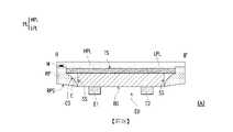
在本發明的一實施例中提出一種發光裝置,包括發光單元,具有本體及二電極,該二電極設置於該本體的底面。螢光膠層,設置於該發光單元的頂面上,該螢光膠膠層具有向下開口的凹槽。透光膠層,設置在該螢光膠層與該發光單元的該本體之間,並覆蓋該本體的部分側表面。至少一黑色標記,形成在該螢光膠層的該凹槽中,且該黑色標記位於該螢光膠層中較接近該些電極的其中之一的一側。白膠反射層,填入該螢光膠層的該凹槽中並環繞該發光單元而設置,該白膠反射層貼附該螢光膠層的下表面、部分該透光膠層及該本體暴露的部分側表面,其中,該發光裝置具有平的側表面,該平的側表面至少包括該白膠反射層,且該白膠反射層具有往該螢光膠層的方向凹陷的下表面,而該白膠反射層與位於該本體側面的部分該透光膠層之間具有傾斜的曲面。In one embodiment of the present invention, a light emitting device is provided, which includes a light emitting unit, has a body and two electrodes, and the two electrodes are disposed on the bottom surface of the body. The fluorescent adhesive layer is arranged on the top surface of the light-emitting unit, and the fluorescent adhesive layer has a groove opening downward. The light-transmitting glue layer is arranged between the fluorescent glue layer and the body of the light-emitting unit, and covers part of the side surface of the body. At least one black mark is formed in the groove of the fluorescent adhesive layer, and the black mark is located on a side of the fluorescent adhesive layer that is closer to one of the electrodes. A reflective layer of white glue, filled in the groove of the fluorescent glue layer and arranged around the light-emitting unit, the reflective layer of white glue attached to the lower surface of the fluorescent glue layer, part of the light-transmitting glue layer and the body The exposed part of the side surface, wherein the light-emitting device has a flat side surface, the flat side surface includes at least the white glue reflective layer, and the white glue reflective layer has a lower surface that is depressed toward the fluorescent glue layer, There is an inclined curved surface between the white glue reflective layer and the part of the light-transmitting glue layer located on the side of the main body.
包括發光單元,具有本體及二電極,該二電極設置於該本體的底面。螢光膠層,設置於該發光單元的頂面上。透光膠層,設置在該螢光膠層與該發光單元的該本體之間,並覆蓋該本體的部分側表面。至少一黑色標記,形成在該螢光膠層的下表面上,且該黑色標記位於該螢光膠層上較接近該些電極的其中之一的一側。白膠反射層,環繞該發光單元而設置,該白膠反射層貼附該螢光膠層的下表面、部分該透光膠層及該本體暴露的部分側表面,其中,該發光裝置具有平的側表面,該平的側表面至少包括該白膠反射層,且該白膠反射層具有往該螢光膠層的方向凹陷的下表面,而該白膠反射層與位於該本體側面的部分該透光膠層之間具有傾斜的曲面。It includes a light-emitting unit with a body and two electrodes, and the two electrodes are arranged on the bottom surface of the body. The fluorescent glue layer is arranged on the top surface of the light emitting unit. The light-transmitting glue layer is arranged between the fluorescent glue layer and the body of the light-emitting unit, and covers part of the side surface of the body. At least one black mark is formed on the lower surface of the fluorescent glue layer, and the black mark is located on the side of the fluorescent glue layer closer to one of the electrodes. A reflective layer of white glue is arranged around the light-emitting unit, and the reflective layer of white glue is attached to the lower surface of the fluorescent glue layer, part of the light-transmitting glue layer and part of the exposed side surface of the body, wherein the light-emitting device has a flat surface The side surface of the flat side surface includes at least the white glue reflective layer, and the white glue reflective layer has a lower surface concave toward the direction of the fluorescent glue layer, and the white glue reflective layer and the part on the side of the main body There is an inclined curved surface between the light-transmitting adhesive layers.
在本發明的一實施例中,上述的螢光膠層更包括彼此堆疊的低濃度螢光膠層以及高濃度螢光膠層。高濃度螢光膠層位於發光單元與低濃度螢光膠層之間。In an embodiment of the present invention, the above-mentioned fluorescent adhesive layer further includes a low-concentration fluorescent adhesive layer and a high-concentration fluorescent adhesive layer stacked on each other. The high-concentration fluorescent adhesive layer is located between the light-emitting unit and the low-concentration fluorescent adhesive layer.
在本發明的一實施例中,上述的螢光膠層的一側設有凹槽。凹槽貫穿高濃度螢光膠層並且暴露出部分的低濃度螢光膠層。凹槽將高濃度螢光膠層分為不同大小的第一部分與第二部分。標記包括暴露的部分低濃度螢光膠層或暴露的部分低濃度螢光膠層以及第一部分與第二部分的至少其中之一。In an embodiment of the present invention, a groove is provided on one side of the above-mentioned fluorescent adhesive layer. The groove runs through the high-concentration fluorescent adhesive layer and exposes part of the low-concentration fluorescent adhesive layer. The groove divides the high-concentration fluorescent adhesive layer into a first part and a second part of different sizes. The mark includes an exposed part of the low-concentration fluorescent adhesive layer or an exposed part of the low-concentration fluorescent adhesive layer and at least one of the first part and the second part.
在本發明的一實施例中,上述的螢光膠層的一側設有一缺角,且缺角作為標記。In an embodiment of the present invention, a notch is provided on one side of the above-mentioned fluorescent adhesive layer, and the notch is used as a mark.
在本發明的一實施例中,上述的螢光膠層的該側設有一刻痕,且刻痕作為標記。In an embodiment of the present invention, a notch is provided on the side of the above-mentioned fluorescent adhesive layer, and the notch is used as a mark.
在本發明的一實施例中,上述的發光裝置更包括反射保護件。反射保護件包覆發光單元以及部分螢光膠層,且至少暴露出二電極及低濃度螢光膠層。In an embodiment of the present invention, the above light emitting device further includes a reflective protection member. The reflective protection member covers the light-emitting unit and part of the fluorescent adhesive layer, and at least exposes two electrodes and the low-concentration fluorescent adhesive layer.
在本發明的一實施例中,上述的反射保護件具有凹面。此凹面往螢光膠層的方向凹陷。In an embodiment of the present invention, the above-mentioned reflective protection member has a concave surface. The concave surface is depressed toward the direction of the fluorescent glue layer.
在本發明的一實施例中,上述的凹面的一側與發光單元接觸,而凹面的一第二側朝向螢光膠層且往遠離發光單元的方向延伸。In an embodiment of the present invention, one side of the above-mentioned concave surface is in contact with the light-emitting unit, and a second side of the concave surface faces the fluorescent adhesive layer and extends away from the light-emitting unit.
在本發明的一實施例中,上述的發光裝置更包括透光膠層。發光單元更包括一連接於頂面與該底面的一側面。透光膠層設置於高濃度螢光膠層上且延伸至發光單元的側面。In an embodiment of the present invention, the above-mentioned light-emitting device further includes a light-transmitting adhesive layer. The light emitting unit further includes a side surface connected to the top surface and the bottom surface. The light-transmitting adhesive layer is disposed on the high-concentration fluorescent adhesive layer and extends to the side of the light-emitting unit.
在本發明的一實施例中提出一種發光裝置的製作方法,包括以下步驟:形成一螢光膠層。對螢光膠層進行第一切割程序,以在螢光膠層中形成多個第一溝槽,以使螢光膠層分為多個部分。各部分作為接合區域。提供多個發光單元,各發光單元包括二電極。分別形成多個標記於螢光膠層的這些部分的一側。將這些發光單元分別接合於這些接合區域。各標記靠近於對應的發光單元的二電極中的一者且遠離於二電極中的另一者。沿著這些第一溝槽進行最終切割程序,以形成多個發光裝置。In one embodiment of the present invention, a method for manufacturing a light-emitting device is provided, including the following steps: forming a fluorescent glue layer. A first cutting process is performed on the fluorescent adhesive layer to form a plurality of first grooves in the fluorescent adhesive layer, so that the fluorescent adhesive layer is divided into multiple parts. Each part acts as a junction area. Multiple light emitting units are provided, and each light emitting unit includes two electrodes. A plurality of marks are respectively formed on one side of these portions of the fluorescent glue layer. These light emitting units are respectively bonded to these bonding regions. Each mark is close to one of the two electrodes of the corresponding light emitting unit and far away from the other of the two electrodes. A final cutting process is performed along the first grooves to form a plurality of light emitting devices.
在本發明的一實施例中,在上述形成該螢光膠層的步驟中更包括以下步驟:形成螢光膠體。靜置螢光膠體,以使螢光膠體分離成彼此堆疊的高濃度螢光膠體與低濃度螢光膠體。固化螢光膠體,以使螢光膠體固化成螢光膠層,其中高濃度螢光膠體與低濃度螢光膠體分別被固化成高濃度螢光膠層與低濃度螢光膠層。In an embodiment of the present invention, the step of forming the fluorescent glue layer further includes the following step: forming fluorescent glue. The fluorescent colloids are allowed to stand still so that the fluorescent colloids are separated into high-concentration fluorescent colloids and low-concentration fluorescent colloids stacked on each other. The fluorescent colloid is cured so that the fluorescent colloid is cured into a fluorescent adhesive layer, wherein the high-concentration fluorescent colloid and the low-concentration fluorescent colloid are respectively cured into a high-concentration fluorescent colloid layer and a low-concentration fluorescent colloid layer.
在本發明的一實施例中,在上述分別形成這些標記於螢光膠層的這些部分的一側的步驟中,更包括:對螢光膠層的這些部分進行第二切割程序,以在螢光膠層的這些部分中分別形成多個第二凹槽。在螢光膠層的每一部分中,第二凹槽貫穿高濃度螢光膠層並且暴露出部分的低濃度螢光膠層,第二凹槽將高濃度螢光膠層分為不同大小的第一部分與第二部分。標記包括暴露的部分低濃度螢光膠層或暴露的部分低濃度螢光膠層以及第一部分與第二部分的至少其中之一。In an embodiment of the present invention, in the step of forming the marks on one side of these parts of the fluorescent adhesive layer, it further includes: performing a second cutting process on these parts of the fluorescent adhesive layer to A plurality of second grooves are respectively formed in these parts of the photoresist layer. In each part of the fluorescent adhesive layer, the second groove runs through the high-concentration fluorescent adhesive layer and exposes a part of the low-concentration fluorescent adhesive layer, and the second groove divides the high-concentration fluorescent adhesive layer into first sections of different sizes. One part and the second part. The mark includes an exposed part of the low-concentration fluorescent adhesive layer or an exposed part of the low-concentration fluorescent adhesive layer and at least one of the first part and the second part.
在本發明的一實施例中,在上述的分別形成這些標記於螢光膠層的這些部分的一側的步驟中,更包括:對螢光膠層的這些部分進行第二切割程序,以在螢光膠層的這些部分中分別形成多個第二凹槽。這些第二凹槽在這些螢光膠層的這些部分中切出多個缺角。第二切割程序的切割方向不同於第一切割程序的切割方向。缺角作為標記。In an embodiment of the present invention, in the above-mentioned steps of forming the marks on one side of these parts of the fluorescent adhesive layer, it further includes: performing a second cutting process on these parts of the fluorescent adhesive layer, so as to A plurality of second grooves are respectively formed in these parts of the fluorescent glue layer. The second grooves cut notches in the portions of the phosphor layers. The cutting direction of the second cutting program is different from the cutting direction of the first cutting program. Notch as a marker.
在本發明的一實施例中,在上述的在分別形成該些標記於該螢光膠層的該些部分的該側的步驟中,更包括:對螢光膠層的這些部分照射雷射光,以使各部分中的低濃度螢光膠層設有一刻痕,且刻痕作為標記。In an embodiment of the present invention, in the above-mentioned step of forming the marks on the side of the portions of the fluorescent adhesive layer, further comprising: irradiating laser light to these portions of the fluorescent adhesive layer, In order to make the low-concentration fluorescent glue layer in each part be provided with a notch, and the notch is used as a mark.
在本發明的一實施例中,在上述的將這些發光單元分別接合於這些接合區域的步驟中,更包括:分別形成多個透光膠層於這些接合區域中的這些高濃度螢光膠層上。將這些發光單元分別藉由這些透光膠層接合於這些高濃度螢光膠層。In an embodiment of the present invention, in the step of bonding the light emitting units to the bonding regions, it further includes: respectively forming a plurality of light-transmitting adhesive layers on the high-concentration fluorescent adhesive layers in the bonding regions superior. The light-emitting units are joined to the high-concentration fluorescent glue layers through the light-transmitting glue layers.
在本發明的一實施例中,更包括:形成反射保護件於螢光膠層上以及這些發光單元之間並填滿這些第一溝槽。反射保護件暴露出這些電極。In an embodiment of the present invention, it further includes: forming a reflective protection member on the fluorescent adhesive layer and between the light emitting units and filling up the first grooves. Reflective protectors expose these electrodes.
在本發明的一實施例中,在上述形成該反射保護件的步驟更包括:靜置反射保護件,以使反射保護件形成往螢光膠層的方向凹陷的凹面。固化反射保護件。In an embodiment of the present invention, the above-mentioned step of forming the reflective protection member further includes: placing the reflective protection member at rest, so that the reflective protection member forms a concave surface concave toward the fluorescent adhesive layer. Cures reflective protectors.
基於上述,在本發明的實施例的發光裝置與其製造方法中,由於螢光膠層上的標記與二電極之間的距離不同,使用者可據此來判斷電極的極性,以大幅地降低將電極接反的機率。Based on the above, in the light-emitting device and its manufacturing method according to the embodiment of the present invention, since the distance between the mark on the fluorescent adhesive layer and the two electrodes is different, the user can judge the polarity of the electrode according to this, so as to greatly reduce the Possibility of electrodes being reversed.
為讓本發明的上述特徵和優點能更明顯易懂,下文特舉實施例,並配合所附圖式作詳細說明如下。In order to make the above-mentioned features and advantages of the present invention more comprehensible, the following specific embodiments are described in detail together with the accompanying drawings.
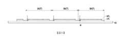
圖1至圖11是用以說明製作本發明的第一實施例的發光裝置的製造流程示意圖。圖12是第一實施例的發光裝置的上視示意圖。圖13是圖12中沿著剖線A-A’的剖面示意圖。1 to 11 are schematic diagrams illustrating the manufacturing process of the light emitting device according to the first embodiment of the present invention. Fig. 12 is a schematic top view of the light emitting device of the first embodiment. Fig. 13 is a schematic cross-sectional view along line A-A' in Fig. 12 .
請參照圖1,提供離型膜30,離型膜30例如是雙面膠膜。接著,於離型膜30上形成螢光膠體PC。螢光膠體PC可由螢光粉與膠體(例如是矽膠(silicone))混合的方法形成。Referring to FIG. 1 , a
請參照圖2,靜置螢光膠體PC一段時間,如24小時後,因重力的關係,螢光膠體PC中的大部分螢光粉會沉澱於下方,而上方仍留有少數的螢光粉,其中上述的靜置時間並不以24小時為限制。也就是說,螢光膠體PC經靜置後會分離成彼此堆疊的高濃度螢光膠體與低濃度螢光膠體。高濃度螢光膠體中的螢光粉濃度大於低濃度螢光膠體中的螢光粉濃度。接著,固化螢光膠體PC,以使螢光膠體PC固化成螢光膠層PL。而高濃度螢光膠體與低濃度螢光膠體亦隨而被分別硬化定型成高濃度螢光膠層HPL與低濃度螢光膠層LPL。固化的方式可例如是透過加熱烘烤的方式,但不以此為限。於本實施例中,整個螢光膠層PL的厚度例如是130微米,但不以此為限。Please refer to Figure 2. After standing the fluorescent colloidal PC for a period of time, such as 24 hours, due to gravity, most of the fluorescent powder in the fluorescent colloidal PC will settle below, while a small amount of fluorescent powder remains on the top , wherein the above standing time is not limited to 24 hours. That is to say, the fluorescent colloid PC will be separated into high-concentration fluorescent colloid and low-concentration fluorescent colloid stacked on each other after standing still. The phosphor concentration in the high-concentration fluorescent colloid is greater than that in the low-concentration fluorescent colloid. Next, the fluorescent colloid PC is cured, so that the fluorescent colloid PC is cured to form the fluorescent colloid layer PL. The high-concentration fluorescent colloid and the low-concentration fluorescent colloid are then hardened and shaped into a high-concentration fluorescent colloid layer HPL and a low-concentration fluorescent colloid layer LPL respectively. The curing method may be, for example, heating and baking, but not limited thereto. In this embodiment, the thickness of the entire phosphor layer PL is, for example, 130 microns, but not limited thereto.
請參照圖3,提供多個發光單元EU(以三個為例,但不以此為限),每一發光單元EU具有彼此相對的頂面TS、底面BS以及連接於頂面TS與底面BS的側面SS,且包括彼此分離的二電極E1、E2。二電極E1、E2中的一者E1可為N型電極,而另一者E2可為P型電極,但不以此為限。發光單元EU例如是發光二極體晶片。Please refer to FIG. 3, a plurality of light-emitting units EU (take three as an example, but not limited thereto), each light-emitting unit EU has a top surface TS opposite to each other, a bottom surface BS, and a top surface TS connected to the bottom surface BS side SS, and includes two electrodes E1, E2 separated from each other. One of the two electrodes E1 and E2 can be an N-type electrode, and the other E2 can be a P-type electrode, but not limited thereto. The light emitting unit EU is, for example, a light emitting diode chip.
請參照圖4,提供另一離型膜40,離型膜40例如亦為雙面膠層。以圖2中的低濃度螢光膠層LPL暴露於外界的表面與離型膜40接合,並將原有的離型膜30移除,以使低濃度螢光膠層LPL位於高濃度螢光膠層HPL與離型膜40之間。換言之,此步驟即為將高濃度螢光膠層HPL與低濃度螢光膠層LPL之間進行一個翻轉並移往另一層離型膜40的動作。Referring to FIG. 4 , another
請參照圖5,對螢光膠層PL進行一第一切割程序,以在螢光膠層PL中形成多個第一溝槽C1,以使螢光膠層PL分為多個部分P。各部分P作為接合區域BA。詳言之,於本實施例中,第一切割程序例如是藉由刀口寬度200微米的切割刀進行切割並下切80微米,以移除部分的高濃度螢光膠層HPL與部分的低濃度螢光膠層LPL,而剩下的高濃度螢光膠層HPL彼此物理性(physically)地分離,因此第一溝槽C1的寬度約為200微米。於此處,所謂的「物理性地分離」係指這些高濃度螢光膠層HPL並沒有直接地連接。應注意的是,切割刀的選用與下切的程度可依據不同的狀況來決定,本發明並不以此為限。Referring to FIG. 5 , a first cutting process is performed on the fluorescent adhesive layer PL to form a plurality of first grooves C1 in the fluorescent adhesive layer PL, so that the fluorescent adhesive layer PL is divided into a plurality of parts P. Each portion P serves as a bonding area BA. Specifically, in this embodiment, the first cutting process is, for example, cutting with a cutting knife with a blade width of 200 microns and cutting down to 80 microns to remove part of the high-concentration fluorescent glue layer HPL and part of the low-concentration fluorescent glue layer. The photoresist layer LPL and the remaining high-concentration phosphor layer HPL are physically separated from each other, so the width of the first trench C1 is about 200 microns. Here, the so-called "physical separation" means that these high-concentration fluorescent glue layers HPL are not directly connected. It should be noted that the selection of the cutting knife and the degree of undercutting can be determined according to different situations, and the present invention is not limited thereto.
請參照圖6,分別形成多個標記M於螢光膠層PL的這些部分P的一側。於本實施例中,形成多個標記M的方式如下:承圖5,再對螢光膠層PL的這些部分P進行第二切割程序,以在螢光膠層PL的這些部分P中分別形成多個第二凹槽C2。詳言之,於本實施例中,第二切割程序例如是藉由刀口寬度50微米的切割刀進行切割並下切80微米,以再次地移除部分的高濃度螢光膠層HPL,因此第二溝槽C2的寬度約為80微米。也就是說,第二溝槽C2的寬度小於第一溝槽C1的寬度。此外,於本實施例中,第二切割程序的切割方向與第一切割程序的切割方向相同。應注意的是,切割刀的選用與下切的程度可依據不同的狀況來決定,本發明並不以此為限。Referring to FIG. 6 , a plurality of marks M are respectively formed on one side of the portions P of the fluorescent adhesive layer PL. In this embodiment, the method of forming a plurality of marks M is as follows: Referring to FIG. 5, the second cutting process is performed on these parts P of the fluorescent adhesive layer PL to form marks in these parts P of the fluorescent adhesive layer PL respectively. A plurality of second grooves C2. Specifically, in this embodiment, the second cutting process is, for example, cutting with a cutting knife with a blade width of 50 microns and undercutting 80 microns to remove part of the high-concentration fluorescent glue layer HPL again. Therefore, the second The width of trench C2 is about 80 microns. That is, the width of the second trench C2 is smaller than the width of the first trench C1. In addition, in this embodiment, the cutting direction of the second cutting procedure is the same as that of the first cutting procedure. It should be noted that the selection of the cutting knife and the degree of undercutting can be determined according to different situations, and the present invention is not limited thereto.
並且,請再參照圖6,在螢光膠層PL的每一部分P中,第二凹槽C2貫穿高濃度螢光膠層HPL並且暴露出部分的低濃度螢光膠層LPL’。第二凹槽C2將高濃度螢光膠層HPL分為較大的第一部分HPL1與較小的第二部分HPL2。暴露的部分低濃度螢光膠層LPL’與第一部分HPL1與第二部分HPL2相鄰。暴露的部分低濃度螢光膠層LPL’與其相鄰的第一部分HPL1與第二部分HPL2可作為標記M。And, please refer to FIG. 6 again, in each part P of the fluorescent glue layer PL, the second groove C2 penetrates through the high-concentration fluorescent glue layer HPL and exposes a part of the low-concentration fluorescent glue layer LPL'. The second groove C2 divides the high-concentration fluorescent glue layer HPL into a larger first portion HPL1 and a smaller second portion HPL2. The exposed part of the low-concentration fluorescent glue layer LPL' is adjacent to the first part HPL1 and the second part HPL2. The exposed part of the low-concentration fluorescent glue layer LPL' and its adjacent first part HPL1 and second part HPL2 can be used as the mark M.
請參照圖7,接著,分別形成多個透光膠層C於該些接合區域BA中的這些高濃度螢光膠層HPL的第一部分HPL1上。透光膠層C例如選用矽膠,但不以此為限。Please refer to FIG. 7 , and then, a plurality of light-transmitting adhesive layers C are respectively formed on the first portions HPL1 of the high-concentration fluorescent adhesive layers HPL in the bonding areas BA. The light-transmitting adhesive layer C is, for example, silicon rubber, but not limited thereto.
請參照圖8,將這些發光單元EU分別藉由這些透光膠層C接合於這些高濃度螢光膠層HPL的第一部分HPL1,並且,標記M靠近於對應的發光單元EU的二電極中E1、E2的一者E2且遠離於二電極E1、E2中的另一者E1。由於毛細現象的關係,透光膠層C具有一曲率的斜面CS,且越靠近發光單元EU的頂面TS,透光膠層C的厚度越厚。此處,透光膠層C的用途在於固定發光單元EU的位置。Please refer to FIG. 8, these light-emitting units EU are respectively connected to the first part HPL1 of these high-concentration fluorescent glue layers HPL through these light-transmitting adhesive layers C, and the mark M is close to the two electrodes E1 of the corresponding light-emitting unit EU One E2 of the two electrodes E1 and E2 is far away from the other E1 of the two electrodes E1 and E2. Due to capillarity, the light-transmitting adhesive layer C has a curvature slope CS, and the closer to the top surface TS of the light-emitting unit EU, the thicker the thickness of the light-transmitting adhesive layer C is. Here, the purpose of the transparent adhesive layer C is to fix the position of the light emitting unit EU.
請參照圖9,形成反射保護件RP於螢光膠層PL上以及這些發光單元EU之間並填滿這些第一溝槽C1與第二溝槽C2。反射保護件RP暴露出這些電極E1、E2。詳細來說,反射保護件RP例如是一白膠層。首先,將反射保護件RP填滿於這些第一溝槽C1與第二溝槽C2。接著,靜置反射保護件RP一段時間後,以使反射保護件RP形成往螢光膠層PL的方向凹陷的一凹面RPS。最後,再加熱固化反射保護件RP,以定型反射保護件RP。Referring to FIG. 9 , a reflective protection member RP is formed on the fluorescent adhesive layer PL and between the light emitting units EU and fills up the first grooves C1 and the second grooves C2 . The reflective protector RP exposes these electrodes E1, E2. In detail, the reflective protection member RP is, for example, a white glue layer. Firstly, the reflective protection member RP is filled in the first trenches C1 and the second trenches C2 . Next, the reflective protector RP is left to stand for a period of time, so that the reflective protector RP forms a concave surface RPS that dents toward the fluorescent glue layer PL. Finally, heat and cure the reflective protector RP to shape the reflective protector RP.
請參照圖10,沿著第一溝槽C1進行最終切割程序,以形成多個發光裝置EA1。至此,發光裝置EA1大體上已製作完成。於本實施例中,發光裝置EA1例如是包括單一個發光單元EU的發光裝置,且例如是晶片級封裝(Chip Scale Package, CSP)的發光裝置EA1。Referring to FIG. 10 , a final cutting process is performed along the first trench C1 to form a plurality of light emitting devices EA1 . So far, the light emitting device EA1 has basically been fabricated. In this embodiment, the light emitting device EA1 is, for example, a light emitting device including a single light emitting unit EU, and is, for example, a chip scale package (Chip Scale Package, CSP) light emitting device EA1.
請參照圖11,再提供又一離型膜50,離型膜50例如亦為雙面膠層或藍膜。以圖10的二電極E1、E2與離型膜50接合,並將原有的離型膜40移除,以使這些發光裝置EA翻轉。Referring to FIG. 11 , another
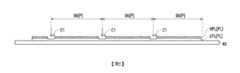
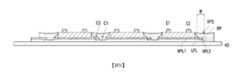
請參照圖12與圖13,於本實施例中,發光裝置EA包括發光單元EU、螢光膠層PL、透光膠層C以及反射保護件RP。發光單元EU具有彼此相對的頂面TS、底面BS與連接於頂面TS與底面BS的側面SS。各發光單元EU包括二電極E1、E2。二電極E1、E2設置於底面BS。螢光膠層PL的一側設有標記M。二電極E1、E2中的一者E2相較於二電極E1、E2中的另一者E1較靠近於標記M。即,電極E2與標記M的平均距離小於電極E1與標記M的平均距離。Please refer to FIG. 12 and FIG. 13 , in this embodiment, the light emitting device EA includes a light emitting unit EU, a fluorescent adhesive layer PL, a transparent adhesive layer C, and a reflective protection member RP. The light emitting unit EU has a top surface TS, a bottom surface BS opposite to each other, and a side surface SS connected to the top surface TS and the bottom surface BS. Each light emitting unit EU includes two electrodes E1, E2. The two electrodes E1 and E2 are disposed on the bottom surface BS. A mark M is provided on one side of the fluorescent glue layer PL. One E2 of the two electrodes E1 , E2 is closer to the mark M than the other E1 of the two electrodes E1 , E2 . That is, the average distance between the electrode E2 and the mark M is smaller than the average distance between the electrode E1 and the mark M.
詳言之,於本實施例中,螢光膠層PL的一側設有第二凹槽C2。第二凹槽C2貫穿高濃度螢光膠層HPL並且暴露出部分的低濃度螢光膠層LPL’。第二凹槽C2將高濃度螢光膠層分為不同大小的第一部分HPL1與第二部分HPL2。標記M包括暴露的部分低濃度螢光膠層LPL’。或者是,暴露的部分低濃度螢光膠層LPL’、第一部分HPL1以及第二部分HPL2的至少其中之一。更詳細來說,由於低濃度螢光膠層LPL與高濃度螢光膠層HPL兩者之間因濃度的關係而顏色不同,沿著方向D來看,可看出螢光膠層PL有不同顏色分佈的狀況,例如是深(對應到高濃度螢光膠層HPL的第一部分HPL1)、淺(對應到被暴露的低濃度螢光膠層LPL)及深(對應到高濃度螢光膠層的第二部分HPL2),而造成了一種顏色的漸層,而此種顏色的漸層可被視為一種標記M,即標記M包括第一部分HPL1、暴露的部分低濃度螢光膠層LPL’以及第二部分HPL2。In detail, in this embodiment, one side of the fluorescent adhesive layer PL is provided with the second groove C2. The second groove C2 runs through the high-concentration fluorescent glue layer HPL and exposes a portion of the low-concentration fluorescent glue layer LPL'. The second groove C2 divides the high-concentration fluorescent glue layer into a first part HPL1 and a second part HPL2 of different sizes. The mark M includes the exposed part of the low concentration fluorescent glue layer LPL'. Or, at least one of the exposed part of the low-concentration fluorescent glue layer LPL', the first part of HPL1 and the second part of HPL2. In more detail, because the color of the low-concentration fluorescent glue layer LPL and the high-concentration fluorescent glue layer HPL are different due to the concentration relationship, looking along the direction D, it can be seen that the fluorescent glue layer PL is different The state of the color distribution, for example, is dark (corresponding to the first part HPL1 of the high-concentration fluorescent glue layer HPL), light (corresponding to the exposed low-concentration fluorescent glue layer LPL) and deep (corresponding to the high-concentration fluorescent glue layer The second part of HPL2), resulting in a color gradient, and this color gradient can be regarded as a mark M, that is, the mark M includes the first part HPL1, the exposed part of the low-concentration fluorescent glue layer LPL' And the second part HPL2.
於另一種觀點來看,因為相鄰於暴露的低濃度螢光膠層LPL’兩側的高濃度螢光膠層HPL的第一部分HPL1與第二部分HPL2的顏色都深於低濃度螢光膠層LPL’的顏色,因此若單就暴露的低濃度螢光膠層LPL’來看也可被視為一種標記M,即標記M包括暴露的低濃度螢光膠層LPL’。或者是,由於位於螢光膠層PL中一側的較小的高濃度螢光膠層HPL的第二部分HPL2與高濃度螢光膠層HPL的第一部分HPL1之間設有低濃度螢光膠層LPL’,因此就高濃度螢光膠層HPL的第一部分HPL1與第二部分HPL2其中之一與低濃度螢光膠層LPL’的組合來看也可被視為一種標記M,即標記M包括高濃度螢光膠層HPL的第一部分HPL1與低濃度螢光膠層LPL’,或者是,標記M包括高濃度螢光膠層HPL的第二部分HPL2與低濃度螢光膠層LPL’,本發明並不以此為限制。From another point of view, because the color of the first part HPL1 and the second part HPL2 of the high-concentration fluorescent glue layer HPL adjacent to the exposed low-concentration fluorescent glue layer LPL' is darker than that of the low-concentration fluorescent glue layer The color of the layer LPL', therefore, can also be regarded as a mark M in terms of the exposed low-concentration fluorescent glue layer LPL', that is, the mark M includes the exposed low-concentration fluorescent glue layer LPL'. Or, since the second part HPL2 of the smaller high-concentration fluorescent glue layer HPL located on one side of the fluorescent glue layer PL and the first part HPL1 of the high-concentration fluorescent glue layer HPL are provided with a low-concentration fluorescent glue Layer LPL', so in terms of the combination of one of the first part HPL1 and the second part HPL2 of the high-concentration fluorescent glue layer HPL and the low-concentration fluorescent glue layer LPL', it can also be regarded as a mark M, that is, the mark M The first part HPL1 of the high-concentration fluorescent glue layer HPL and the low-concentration fluorescent glue layer LPL', or the mark M includes the second part HPL2 of the high-concentration fluorescent glue layer HPL and the low-concentration fluorescent glue layer LPL', The present invention is not limited thereto.
於本實施例中,反射保護件RP包覆發光單元EU以及部分螢光膠層PL,且至少暴露出二電極E1、E2及低濃度螢光膠層LPL。反射保護件RP具有朝向外界的凹面RPS。此凹面RPS往螢光膠層PL方向凹陷。凹面RPS的一側與發光單元EU接觸,而凹面RPS的第二側朝向螢光膠層PL且往遠離發光單元EU的方向延伸。當本實施例的發光裝置EA1後續要與外接基板(例如是顯示面板中的背板、印刷電路板或其他種類的基板)進行連接時,透過反射保護件RP為暴露於外界的表面為凹面RPS的設計,可以避免反射保護件RP與外接基板之間因反射保護件RP凸出而使發光裝置EA與外界基板之間間隔出間隙,此間隙的產生會導致發光單元EA的電極M1、M2無法良好地接合於外接基板。In this embodiment, the reflective protection member RP covers the light emitting unit EU and part of the fluorescent glue layer PL, and at least exposes the two electrodes E1, E2 and the low-concentration fluorescent glue layer LPL. The reflective protector RP has a concave surface RPS facing the outside. The concave surface RPS is depressed toward the direction of the fluorescent glue layer PL. One side of the concave surface RPS is in contact with the light emitting unit EU, and a second side of the concave surface RPS faces the fluorescent glue layer PL and extends away from the light emitting unit EU. When the light-emitting device EA1 of this embodiment is subsequently connected to an external substrate (such as a backplane in a display panel, a printed circuit board, or other types of substrates), the surface exposed to the outside world through the reflection protection member RP is a concave surface RPS The design can avoid the gap between the light-emitting device EA and the external substrate due to the protrusion of the reflective protection part RP and the external substrate. The generation of this gap will cause the electrodes M1 and M2 of the light-emitting unit EA to fail Good bonding to external substrates.
於本實施例中,透光膠層C設置於高濃度螢光膠層HPL上且延伸至發光單元EU的側面SS。In this embodiment, the light-transmitting adhesive layer C is disposed on the high-concentration fluorescent adhesive layer HPL and extends to the side SS of the light emitting unit EU.
承上述,在本發明的實施例的發光裝置與其製造方法中,由於螢光膠層PL上設有標記M,且此標記M分別與二電極之間任一電極E1、E2的平均距離不同。因此,當這些發光裝置EA製造完成時,可告知使用者較靠近標記M的電極E2例如是作為P型電極,因此使用者就可以清楚地知道電極E2為P型電極,而電極E1則為電性相反的N型電極。簡言之,使用者可根據標記M與電極E1、E2之間的距離關係可簡單地判斷電極極性,以大幅地降低將電極接反的機率。Based on the above, in the light-emitting device and its manufacturing method according to the embodiment of the present invention, since the mark M is provided on the fluorescent glue layer PL, and the average distance between the mark M and any electrode E1, E2 between the two electrodes is different. Therefore, when these light-emitting devices EA are manufactured, the user can be informed that the electrode E2 closer to the mark M is used as a P-type electrode, for example, so the user can clearly know that the electrode E2 is a P-type electrode, and the electrode E1 is an electrode. opposite N-type electrodes. In short, the user can simply judge the polarity of the electrodes according to the distance relationship between the mark M and the electrodes E1 and E2, so as to greatly reduce the probability of reversely connecting the electrodes.
圖14至圖19是用以說明製作本發明的第二實施例的發光裝置的製造流程示意圖。圖20是第二實施例的發光裝置的上視示意圖。14 to 19 are schematic diagrams illustrating the manufacturing process of the light emitting device according to the second embodiment of the present invention. Fig. 20 is a schematic top view of the light emitting device of the second embodiment.
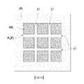
第二實施例的發光裝置EA2的製造流程中的部分步驟類似於第一實施例的發光裝置EA的製造流程,於以下的說明中僅就對其差異進行說明。Some steps in the manufacturing process of the light emitting device EA2 of the second embodiment are similar to the manufacturing process of the light emitting device EA of the first embodiment, and only the differences are described in the following description.
承圖1至圖4的步驟後,請參照圖5以及圖14,於本實施例中,在螢光膠層PL中形成多個第一溝槽C1,以使螢光膠層PL分為多個部分P(以九個部分P為例,但不以此為限)。第一溝槽C1的延伸方向大致上與螢光膠層PL的每一個部分P的二對邊平行。After following the steps in Figures 1 to 4, please refer to Figures 5 and 14. In this embodiment, a plurality of first grooves C1 are formed in the fluorescent adhesive layer PL, so that the fluorescent adhesive layer PL is divided into multiple grooves. Parts P (taking nine parts P as an example, but not limited thereto). The extending direction of the first trench C1 is substantially parallel to two opposite sides of each portion P of the phosphor layer PL.
請參照圖15,分別形成多個標記M於螢光膠層PL的這些部分P的一側。於本實施例中,形成多個標記M的方式如下:承圖14,再對螢光膠層PL的這些部分P進行第二切割程序,以在螢光膠層PL的這些部分P中分別形成多個第二凹槽C2。詳言之,於本實施例中,第二切割程序大致上類似於圖6的步驟,其主要差異在於:在進行第二切割程序之前,先將整個離型膜(未示出)以一角度旋轉,接著,再進行第二切割程序。因此,第二切割程序的切割方向與第一切割程序的切割方向具有一夾角,且此夾角例如是45度,但不以此為限。由圖15可知,第一凹槽C1的延伸方向不同於第二凹槽C2的延伸方向。Referring to FIG. 15 , a plurality of marks M are respectively formed on one side of the portions P of the fluorescent adhesive layer PL. In this embodiment, the method of forming a plurality of marks M is as follows: Referring to FIG. 14 , the second cutting process is performed on these parts P of the fluorescent adhesive layer PL to form marks in these parts P of the fluorescent adhesive layer PL respectively. A plurality of second grooves C2. Specifically, in the present embodiment, the second cutting procedure is substantially similar to the step of FIG. Rotate, then, carry out the second cutting procedure again. Therefore, the cutting direction of the second cutting procedure has an included angle with the cutting direction of the first cutting procedure, and the included angle is, for example, 45 degrees, but not limited thereto. It can be seen from FIG. 15 that the extending direction of the first groove C1 is different from the extending direction of the second groove C2.
請參照圖16,分別形成多個透光膠層C於該些接合區域BA中的這些高濃度螢光膠層HPL的第一部分HPL1上。應注意的是,由於第二切割程序的關係,有些部分P中的高濃度螢光膠層HPL2其中央處被切割,因此不適合進行後續的接合程序。因此,於圖16中,形成多個透光膠層C的位置係以形成有切角(標記M)的部分P為主。Referring to FIG. 16 , a plurality of light-transmitting adhesive layers C are respectively formed on the first portions HPL1 of the high-concentration fluorescent adhesive layers HPL in the bonding areas BA. It should be noted that due to the second cutting procedure, the central part of the high-concentration fluorescent adhesive layer HPL2 in some parts P is cut, and thus is not suitable for the subsequent joining procedure. Therefore, in FIG. 16 , the positions where a plurality of light-transmitting adhesive layers C are formed are mainly the portion P where a chamfered corner (marked M) is formed.
請參照圖18,形成反射保護件RP於螢光膠層PL上以及這些發光單元EU之間並填滿第一溝槽、第二溝槽。反射保護件RP暴露出這些電極E1、E2。Referring to FIG. 18 , a reflective protection member RP is formed on the fluorescent adhesive layer PL and between the light emitting units EU and fills up the first groove and the second groove. The reflective protector RP exposes these electrodes E1, E2.
請參照圖19,沿著第一溝槽C1進行最終切割程序,以形成多個發光裝置EA2。至此,發光裝置EA2大體上已製作完成。Referring to FIG. 19 , a final cutting process is performed along the first trench C1 to form a plurality of light emitting devices EA2 . So far, the light emitting device EA2 has been substantially completed.
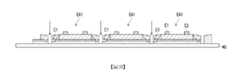
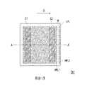
請參照圖20,本實施例中的發光裝置EA2大體上類似於圖12與圖13的發光裝置EA,其主要差異在於:發光裝置EA2的螢光膠層PL一側設有缺角,且此缺角作為標記M。Please refer to FIG. 20 , the light emitting device EA2 in this embodiment is generally similar to the light emitting device EA in FIG. 12 and FIG. The missing corner is marked M.
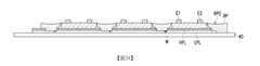
圖21至圖26是用以說明製作本發明的第三實施例的發光裝置的製造流程示意圖。圖27是第三實施例的發光裝置的上視示意圖。圖28是圖27中沿著剖線B-B’的剖面示意圖。21 to 26 are schematic diagrams illustrating the manufacturing process of the light emitting device according to the third embodiment of the present invention. Fig. 27 is a schematic top view of the light emitting device of the third embodiment. Fig. 28 is a schematic cross-sectional view along the section line B-B' in Fig. 27.
第三實施例的發光裝置EA3的製造流程中的部分步驟類似於第一實施例的發光裝置EA的製造流程,於以下的說明中僅就對其差異進行說明。Some steps in the manufacturing process of the light emitting device EA3 of the third embodiment are similar to the manufacturing process of the light emitting device EA of the first embodiment, and only the differences are described in the following description.
承圖1至圖5的步驟後,請參照圖21,對螢光膠層PL的這些部分P以照射雷射光,以使各部分P中的低濃度螢光膠層LPL因雷射光的照射而黑化,而於低濃度螢光膠層LPL上形成雷射刻痕,且雷射刻痕作為標記M。此外,於本例中,雷射刻痕的態樣為條狀,於其他的實施例中,亦可以圓形、方形或其他形狀的圖案,本發明並不此以為限。After following the steps in Figures 1 to 5, please refer to Figure 21 to irradiate these parts P of the fluorescent adhesive layer PL with laser light, so that the low-concentration fluorescent adhesive layer LPL in each part P is irradiated by laser light. blackening, and form a laser score on the low-concentration fluorescent glue layer LPL, and the laser score is used as a mark M. In addition, in this example, the shape of the laser marking is striped, and in other embodiments, it can also be circular, square or other shapes, and the present invention is not limited thereto.
接著,於圖22至圖26的步驟中,大致上類似於圖7至圖11的步驟,於此不再贅述。Next, the steps in FIG. 22 to FIG. 26 are substantially similar to the steps in FIG. 7 to FIG. 11 , and will not be repeated here.
請參照圖27與圖28,本實施例中的發光裝置EA3大體上類似於圖12與圖13的發光裝置EA,其主要差異在於:發光裝置EA3的螢光膠層PL一側設有雷射刻痕,且此刻痕作為標記M。此外,於本實施例中,標記M例如是靠近於作為N型電極的電極E1中,但本發明並不以此為限制。Please refer to FIG. 27 and FIG. 28. The light emitting device EA3 in this embodiment is generally similar to the light emitting device EA in FIG. 12 and FIG. Notch, and this notch as a mark M. In addition, in this embodiment, the mark M is, for example, close to the electrode E1 which is an N-type electrode, but the present invention is not limited thereto.
應注意的是,在本發明上述的實施例中,標記M的態樣例如是刻痕、缺角、與高低濃度螢光膠層之間形成的不同顏色的漸層,於其他的實施例中,標記M的態樣例如亦可以為圓形缺口、三角形缺口或其他的多邊形缺口或者是其他可以以肉眼明顯看出的標記,本發明並不以此為限。It should be noted that in the above-mentioned embodiments of the present invention, the form of the mark M is, for example, a notch, a missing corner, and a gradient of different colors formed between the high and low concentration fluorescent adhesive layers. In other embodiments The form of the mark M, for example, can also be a circular notch, a triangular notch or other polygonal notches or other marks that can be clearly seen by naked eyes, and the present invention is not limited thereto.
綜上所述,在本發明的實施例的發光裝置與其製造方法中,由於螢光膠層上設有與二電極之間分別具有不同距離的標記,因此使用者可根據標記與二電極之間的相對位置關係來判斷電極的極性,可大幅地降低將電極接反的機率。To sum up, in the light-emitting device and its manufacturing method according to the embodiment of the present invention, since the fluorescent adhesive layer is provided with marks having different distances from the two electrodes, the user can determine the distance between the mark and the two electrodes. The relative positional relationship of the electrodes can be used to determine the polarity of the electrodes, which can greatly reduce the probability of reversed electrodes.
雖然本發明已以實施例揭露如上,然其並非用以限定本發明,任何所屬技術領域中具有通常知識者,在不脫離本發明的精神和範圍內,當可作些許的更動與潤飾,故本發明的保護範圍當視後附的申請專利範圍所界定者為準。Although the present invention has been disclosed above with the embodiments, it is not intended to limit the present invention. Anyone with ordinary knowledge in the technical field may make some changes and modifications without departing from the spirit and scope of the present invention. The scope of protection of the present invention should be defined by the scope of the appended patent application.
30、40、50:離型膜 A-A’、B-B’:剖線 BA:接合區域 BS:底面 C:透光膠層 C1:第一溝槽 C2:第二溝槽 CS:斜面 EA1~EA3:發光裝置 EU:發光單元 E1、E2:電極 HPL:高濃度螢光膠層 HPL1:高濃度螢光膠層的第一部分 HPL2:高濃度螢光膠層的第二部分 LPL:低濃度螢光膠層 LPL’:暴露的部分低濃度螢光膠層 M:標記 P:部分 PC:螢光膠體 PL:螢光膠層 RP:反射保護件 RPS:凹面 SS:側面 TS:頂面30, 40, 50: release film A-A', B-B': section line BA: joint area BS: bottom surface C: Translucent adhesive layer C1: first groove C2: second groove CS: inclined plane EA1~EA3: Lighting device EU: Luminous Unit E1, E2: electrodes HPL: high concentration fluorescent glue layer HPL1: the first part of the high concentration fluorescent glue layer HPL2: The second part of the high concentration fluorescent glue layer LPL: low concentration fluorescent glue layer LPL': The exposed part of the low-concentration fluorescent glue layer M: mark P: part PC: fluorescent colloid PL: fluorescent glue layer RP: reflective protection RPS: Concave SS: side TS: top surface
圖1至圖11是用以說明製作本發明的第一實施例的發光裝置的製造流程示意圖。 圖12是第一實施例的發光裝置的上視示意圖。 圖13是圖12中沿著剖線A-A’的剖面示意圖。 圖14至圖19是用以說明製作本發明的第二實施例的發光裝置的製造流程示意圖。 圖20是第二實施例的發光裝置的上視示意圖。 圖21至圖26是用以說明製作本發明的第三實施例的發光裝置的製造流程示意圖。 圖27是第三實施例的發光裝置的上視示意圖。 圖28是圖27中沿著剖線B-B’的剖面示意圖。1 to 11 are schematic diagrams illustrating the manufacturing process of the light emitting device according to the first embodiment of the present invention. Fig. 12 is a schematic top view of the light emitting device of the first embodiment. Fig. 13 is a schematic cross-sectional view along line A-A' in Fig. 12 . 14 to 19 are schematic diagrams illustrating the manufacturing process of the light emitting device according to the second embodiment of the present invention. Fig. 20 is a schematic top view of the light emitting device of the second embodiment. 21 to 26 are schematic diagrams illustrating the manufacturing process of the light emitting device according to the third embodiment of the present invention. Fig. 27 is a schematic top view of the light emitting device of the third embodiment. Fig. 28 is a schematic cross-sectional view along the section line B-B' in Fig. 27.
A-A’:剖線A-A': section line
BS:底面BS: bottom surface
C:透光膠層C: Translucent adhesive layer
CS:斜面CS: inclined plane
C2:第二溝槽C2: second groove
D:方向D: Direction
EA1:發光裝置EA1: Lighting device
EU:發光單元EU: Luminous Unit
E1、E2:電極E1, E2: electrodes
HPL:高濃度螢光膠層HPL: high concentration fluorescent glue layer
HPL1:高濃度螢光膠層的第一部分HPL1: the first part of the high concentration fluorescent glue layer
HPL2:高濃度螢光膠層的第二部分HPL2: The second part of the high concentration fluorescent glue layer
LPL:低濃度螢光膠層LPL: low concentration fluorescent glue layer
LPL’:暴露的部分低濃度螢光膠層LPL': The exposed part of the low-concentration fluorescent glue layer
M:標記M: mark
PL:螢光膠層PL: fluorescent glue layer
RP:反射保護件RP: reflective protection
RPS:凹面RPS: Concave
SS:側面SS: side
TS:頂面TS: top surface
Claims (10)
Translated fromChineseApplications Claiming Priority (2)
| Application Number | Priority Date | Filing Date | Title |
|---|---|---|---|
| US201762581763P | 2017-11-05 | 2017-11-05 | |
| US62/581,763 | 2017-11-05 |
Publications (1)
| Publication Number | Publication Date |
|---|---|
| TW202249306Atrue TW202249306A (en) | 2022-12-16 |
Family
ID=66401453
Family Applications (2)
| Application Number | Title | Priority Date | Filing Date |
|---|---|---|---|
| TW111132384ATW202249306A (en) | 2017-11-05 | 2018-11-05 | Light emitting apparatus |
| TW107139198ATWI778167B (en) | 2017-11-05 | 2018-11-05 | Light emitting apparatus and manufacturing method thereof |
Family Applications After (1)
| Application Number | Title | Priority Date | Filing Date |
|---|---|---|---|
| TW107139198ATWI778167B (en) | 2017-11-05 | 2018-11-05 | Light emitting apparatus and manufacturing method thereof |
Country Status (3)
| Country | Link |
|---|---|
| US (1) | US10854780B2 (en) |
| CN (1) | CN109755220B (en) |
| TW (2) | TW202249306A (en) |
Families Citing this family (5)
| Publication number | Priority date | Publication date | Assignee | Title |
|---|---|---|---|---|
| DE102019116103B4 (en)* | 2019-06-13 | 2021-04-22 | Notion Systems GmbH | Method for labeling a printed circuit board by creating shading in a functional lacquer layer |
| TWI764341B (en)* | 2020-04-07 | 2022-05-11 | 億光電子工業股份有限公司 | Light-emitting device |
| USD996377S1 (en)* | 2022-02-17 | 2023-08-22 | Creeled, Inc. | Light-emitting diode package |
| USD996378S1 (en) | 2022-03-09 | 2023-08-22 | Creeled, Inc. | Light-emitting diode package |
| US12355013B2 (en) | 2022-04-21 | 2025-07-08 | Creeled, Inc. | Emission height arrangements in light-emitting diode packages and related devices and methods |
Family Cites Families (105)
| Publication number | Priority date | Publication date | Assignee | Title |
|---|---|---|---|---|
| US6155699A (en) | 1999-03-15 | 2000-12-05 | Agilent Technologies, Inc. | Efficient phosphor-conversion led structure |
| JP3866058B2 (en) | 2001-07-05 | 2007-01-10 | シャープ株式会社 | Semiconductor device, wiring board and tape carrier |
| TW567619B (en) | 2001-08-09 | 2003-12-21 | Matsushita Electric Industrial Co Ltd | LED lighting apparatus and card-type LED light source |
| KR100447867B1 (en) | 2001-10-05 | 2004-09-08 | 삼성전자주식회사 | Semiconductor package |
| US6952079B2 (en) | 2002-12-18 | 2005-10-04 | General Electric Company | Luminaire for light extraction from a flat light source |
| JP3716252B2 (en) | 2002-12-26 | 2005-11-16 | ローム株式会社 | Light emitting device and lighting device |
| TWI220076B (en) | 2003-08-27 | 2004-08-01 | Au Optronics Corp | Light-emitting device |
| JP4516337B2 (en) | 2004-03-25 | 2010-08-04 | シチズン電子株式会社 | Semiconductor light emitting device |
| JP4667803B2 (en) | 2004-09-14 | 2011-04-13 | 日亜化学工業株式会社 | Light emitting device |
| TWI244228B (en) | 2005-02-03 | 2005-11-21 | United Epitaxy Co Ltd | Light emitting device and manufacture method thereof |
| KR100640496B1 (en) | 2005-11-23 | 2006-11-01 | 삼성전기주식회사 | Vertical GaN-based Light-Emitting Diode Device |
| US7889421B2 (en) | 2006-11-17 | 2011-02-15 | Rensselaer Polytechnic Institute | High-power white LEDs and manufacturing method thereof |
| US8252615B2 (en) | 2006-12-22 | 2012-08-28 | Stats Chippac Ltd. | Integrated circuit package system employing mold flash prevention technology |
| US8552444B2 (en) | 2007-11-19 | 2013-10-08 | Panasonic Corporation | Semiconductor light-emitting device and manufacturing method of the same |
| EP2216834B1 (en) | 2007-11-29 | 2017-03-15 | Nichia Corporation | Light-emitting apparatus |
| CN101459212B (en)* | 2007-12-11 | 2011-06-22 | 富士迈半导体精密工业(上海)有限公司 | solid state light emitting device |
| TWI380466B (en)* | 2007-12-31 | 2012-12-21 | Foxsemicon Integrated Tech Inc | Solid illuminating element, solid illuminator, and method for manufacturing the solid illuminating element |
| GB0801509D0 (en) | 2008-01-28 | 2008-03-05 | Photonstar Led Ltd | Light emitting system with optically transparent thermally conductive element |
| EP2269239A2 (en) | 2008-03-21 | 2011-01-05 | Koninklijke Philips Electronics N.V. | A luminous device |
| JP2009245981A (en) | 2008-03-28 | 2009-10-22 | Toyota Central R&D Labs Inc | Led light-emitting device |
| TWI416755B (en) | 2008-05-30 | 2013-11-21 | Epistar Corp | Light source module, corresponding light bar and corresponding liquid crystal display device thereof |
| US7973327B2 (en) | 2008-09-02 | 2011-07-05 | Bridgelux, Inc. | Phosphor-converted LED |
| US7825427B2 (en) | 2008-09-12 | 2010-11-02 | Bridgelux, Inc. | Method and apparatus for generating phosphor film with textured surface |
| US7928655B2 (en) | 2008-11-10 | 2011-04-19 | Visera Technologies Company Limited | Light-emitting diode device and method for fabricating the same |
| CN101515621B (en) | 2009-02-19 | 2011-03-30 | 旭丽电子(广州)有限公司 | Light emitting diode chip, manufacturing method and packaging method |
| CN101834236B (en) | 2009-03-11 | 2013-02-13 | 晶元光电股份有限公司 | light emitting device |
| US8317384B2 (en) | 2009-04-10 | 2012-11-27 | Intellectual Discovery Co., Ltd. | Light guide film with cut lines, and optical keypad using such film |
| JP5482378B2 (en) | 2009-04-20 | 2014-05-07 | 日亜化学工業株式会社 | Light emitting device |
| US9006763B2 (en) | 2009-05-22 | 2015-04-14 | Panasonic Intellectual Property Management Co., Ltd. | Semiconductor light-emitting device and light source device using the same |
| US8097894B2 (en) | 2009-07-23 | 2012-01-17 | Koninklijke Philips Electronics N.V. | LED with molded reflective sidewall coating |
| TWI403003B (en) | 2009-10-02 | 2013-07-21 | Chi Mei Lighting Tech Corp | Light-emitting diode and manufacturing method thereof |
| DE112011100376B4 (en) | 2010-01-29 | 2024-06-27 | Citizen Electronics Co., Ltd. | METHOD FOR PRODUCING A LIGHT-EMITTING DEVICE |
| BR112012020317B1 (en) | 2010-02-09 | 2020-10-13 | Nichia Corporation | light emitting device |
| EP2378576A2 (en) | 2010-04-15 | 2011-10-19 | Samsung LED Co., Ltd. | Light emitting diode package, lighting apparatus having the same, and method for manufacturing light emitting diode package |
| JP5390472B2 (en) | 2010-06-03 | 2014-01-15 | 株式会社東芝 | Semiconductor light emitting device and manufacturing method thereof |
| JP5414627B2 (en) | 2010-06-07 | 2014-02-12 | 株式会社東芝 | Semiconductor light emitting device and manufacturing method thereof |
| JP5572013B2 (en) | 2010-06-16 | 2014-08-13 | スタンレー電気株式会社 | Light emitting device and manufacturing method thereof |
| CN102315354B (en) | 2010-06-29 | 2013-11-06 | 展晶科技(深圳)有限公司 | Packaging structure of light emitting diode |
| JP5486431B2 (en) | 2010-07-27 | 2014-05-07 | 日東電工株式会社 | LIGHT EMITTING DEVICE COMPONENT, LIGHT EMITTING DEVICE, AND ITS MANUFACTURING METHOD |
| JP2012033823A (en) | 2010-08-02 | 2012-02-16 | Stanley Electric Co Ltd | Light emitting device and method for manufacturing the same |
| CN102376860A (en)* | 2010-08-05 | 2012-03-14 | 夏普株式会社 | Light emitting apparatus and method for manufacturing thereof |
| CN201910421U (en) | 2010-12-01 | 2011-07-27 | 宝创科技股份有限公司 | Planar Structure of Light Emitting Diode Devices |
| US8581287B2 (en) | 2011-01-24 | 2013-11-12 | Stanley Electric Co., Ltd. | Semiconductor light emitting device having a reflective material, wavelength converting layer and optical plate with rough and plane surface regions, and method of manufacturing |
| JP5647028B2 (en) | 2011-02-14 | 2014-12-24 | スタンレー電気株式会社 | Light emitting device and manufacturing method thereof |
| TWI525858B (en) | 2011-02-15 | 2016-03-11 | Light emitting diode package structure | |
| CN102683514B (en) | 2011-03-06 | 2017-07-14 | 维亚甘有限公司 | LED package and manufacture method |
| KR20120106568A (en) | 2011-03-18 | 2012-09-26 | 가부시키가이샤 한도오따이 에네루기 켄큐쇼 | Light-emitting device and manufacturing method thereof |
| US20120261689A1 (en) | 2011-04-13 | 2012-10-18 | Bernd Karl Appelt | Semiconductor device packages and related methods |
| JP5745319B2 (en) | 2011-04-14 | 2015-07-08 | 日東電工株式会社 | Fluorescent reflection sheet and method for manufacturing light emitting diode device |
| JP5777705B2 (en) | 2011-04-20 | 2015-09-09 | 株式会社エルム | Light emitting device and manufacturing method thereof |
| JP5680472B2 (en) | 2011-04-22 | 2015-03-04 | シチズンホールディングス株式会社 | Manufacturing method of semiconductor light emitting device |
| CN107768502B (en) | 2011-05-16 | 2019-07-05 | 日亚化学工业株式会社 | Light-emitting device and method of manufacturing the same |
| TW201248725A (en) | 2011-05-31 | 2012-12-01 | Aceplux Optotech Inc | Epitaxial substrate with transparent cone, LED, and manufacturing method thereof. |
| JP5848562B2 (en) | 2011-09-21 | 2016-01-27 | シチズン電子株式会社 | Semiconductor light emitting device and manufacturing method thereof. |
| JP5893888B2 (en) | 2011-10-13 | 2016-03-23 | シチズン電子株式会社 | Semiconductor light emitting device |
| TW201318221A (en) | 2011-10-26 | 2013-05-01 | Episil Technologies Inc | Light-emitting diode crucible bracket and manufacturing method thereof |
| KR101905535B1 (en) | 2011-11-16 | 2018-10-10 | 엘지이노텍 주식회사 | Light emitting device and light apparatus having thereof |
| TW201327926A (en) | 2011-12-30 | 2013-07-01 | Ind Tech Res Inst | Light conversion structure and the light emitting device packaging structure using the same |
| JP5956167B2 (en) | 2012-01-23 | 2016-07-27 | スタンレー電気株式会社 | LIGHT EMITTING DEVICE, VEHICLE LIGHT, AND METHOD FOR MANUFACTURING LIGHT EMITTING DEVICE |
| KR101957700B1 (en) | 2012-02-01 | 2019-03-14 | 삼성전자주식회사 | Ligt Emitting Device |
| US8946747B2 (en) | 2012-02-13 | 2015-02-03 | Cree, Inc. | Lighting device including multiple encapsulant material layers |
| US9240530B2 (en) | 2012-02-13 | 2016-01-19 | Cree, Inc. | Light emitter devices having improved chemical and physical resistance and related methods |
| US9735198B2 (en) | 2012-03-30 | 2017-08-15 | Cree, Inc. | Substrate based light emitter devices, components, and related methods |
| TWI495056B (en) | 2012-04-24 | 2015-08-01 | Genesis Photonics Inc | Substrate structure |
| JP5816127B2 (en) | 2012-04-27 | 2015-11-18 | 株式会社東芝 | Semiconductor light emitting device and manufacturing method thereof |
| US20140009060A1 (en) | 2012-06-29 | 2014-01-09 | Nitto Denko Corporation | Phosphor layer-covered led, producing method thereof, and led device |
| CN103515520B (en) | 2012-06-29 | 2016-03-23 | 展晶科技(深圳)有限公司 | Package structure for LED and manufacture method thereof |
| CN103531669B (en) | 2012-07-05 | 2016-09-07 | 北京时代浩鼎科技股份有限公司 | The manufacture method of package structure for LED |
| US9287475B2 (en) | 2012-07-20 | 2016-03-15 | Cree, Inc. | Solid state lighting component package with reflective polymer matrix layer |
| DE102012107290A1 (en) | 2012-08-08 | 2014-02-13 | Osram Opto Semiconductors Gmbh | Optoelectronic semiconductor device, conversion agent platelets and method of making a conversion agent platelet |
| JP6099901B2 (en) | 2012-08-23 | 2017-03-22 | スタンレー電気株式会社 | Light emitting device |
| JP6149487B2 (en) | 2012-11-09 | 2017-06-21 | 日亜化学工業株式会社 | LIGHT EMITTING DEVICE MANUFACTURING METHOD AND LIGHT EMITTING DEVICE |
| JP2014112669A (en) | 2012-11-12 | 2014-06-19 | Citizen Holdings Co Ltd | Semiconductor light-emitting device and manufacturing method of the same |
| CN104854716B (en) | 2012-12-10 | 2017-06-20 | 西铁城时计株式会社 | LED device and manufacturing method thereof |
| TWM453969U (en) | 2012-12-26 | 2013-05-21 | Genesis Photonics Inc | Light emitting device |
| CN103137571A (en) | 2013-01-22 | 2013-06-05 | 日月光半导体制造股份有限公司 | Semiconductor package structure and manufacturing method thereof |
| US9318674B2 (en)* | 2013-02-05 | 2016-04-19 | Cree, Inc. | Submount-free light emitting diode (LED) components and methods of fabricating same |
| JP5819335B2 (en) | 2013-02-18 | 2015-11-24 | 株式会社東芝 | Semiconductor light emitting device and manufacturing method thereof |
| JP2014170902A (en) | 2013-03-05 | 2014-09-18 | Toshiba Corp | Semiconductor light-emitting device and manufacturing method of the same |
| FR3003403B1 (en) | 2013-03-14 | 2016-11-04 | Commissariat Energie Atomique | METHOD FOR FORMING LIGHT EMITTING DIODES |
| CN103199183B (en) | 2013-04-08 | 2016-01-27 | 厦门市三安光电科技有限公司 | A kind of encapsulating structure improving vertical LED chip brightness |
| TWI540766B (en) | 2013-07-10 | 2016-07-01 | 隆達電子股份有限公司 | Light emitting diode package structure |
| CN104347610B (en) | 2013-07-23 | 2017-06-20 | 深圳市瑞丰光电子股份有限公司 | Embedded LED device and preparation method thereof and luminaire |
| KR20150042362A (en) | 2013-10-10 | 2015-04-21 | 삼성전자주식회사 | Light emitting diode package and method of manufacturing the same |
| TWI520383B (en) | 2013-10-14 | 2016-02-01 | 新世紀光電股份有限公司 | Light emitting diode package structure |
| TWI533478B (en)* | 2013-10-14 | 2016-05-11 | 新世紀光電股份有限公司 | Flip-chip LED package structure |
| CN103531725A (en) | 2013-10-16 | 2014-01-22 | 上海和辉光电有限公司 | Electroluminescent component and packaging method thereof |
| JP6182050B2 (en) | 2013-10-28 | 2017-08-16 | 株式会社東芝 | Semiconductor light emitting device |
| US9419189B1 (en) | 2013-11-04 | 2016-08-16 | Soraa, Inc. | Small LED source with high brightness and high efficiency |
| KR102075993B1 (en) | 2013-12-23 | 2020-02-11 | 삼성전자주식회사 | Method of Fabricating White LED Devices |
| JP6244906B2 (en)* | 2013-12-27 | 2017-12-13 | 日亜化学工業株式会社 | Semiconductor light emitting device |
| TWI542047B (en) | 2014-01-13 | 2016-07-11 | 邱羅利士公司 | Light-emitting diode package structure |
| KR101584201B1 (en)* | 2014-01-13 | 2016-01-13 | 삼성전자주식회사 | Semiconductor light emitting device |
| JP2015173142A (en) | 2014-03-11 | 2015-10-01 | 株式会社東芝 | Semiconductor light emitting device |
| TWI557955B (en) | 2014-04-23 | 2016-11-11 | 光寶光電(常州)有限公司 | Led carrier and manufacturing method thereof |
| US9997676B2 (en) | 2014-05-14 | 2018-06-12 | Genesis Photonics Inc. | Light emitting device and manufacturing method thereof |
| CN106129231B (en)* | 2015-05-05 | 2019-11-22 | 新世纪光电股份有限公司 | Light emitting device and manufacturing method thereof |
| CN203910851U (en) | 2014-05-23 | 2014-10-29 | 晶科电子(广州)有限公司 | White light LED chip |
| CN104253194A (en) | 2014-09-18 | 2014-12-31 | 易美芯光(北京)科技有限公司 | Structure and method for packaging of chip-size white LED (light emitting diode) |
| US20160181476A1 (en) | 2014-12-17 | 2016-06-23 | Apple Inc. | Micro led with dielectric side mirror |
| US20160190406A1 (en) | 2014-12-24 | 2016-06-30 | Epistar Corporation | Light-emitting device and manufacturing method thereof |
| JP6554914B2 (en)* | 2015-06-01 | 2019-08-07 | 日亜化学工業株式会社 | Light emitting device and manufacturing method thereof |
| CN106549092A (en) | 2015-09-18 | 2017-03-29 | 新世纪光电股份有限公司 | Light emitting device and method for manufacturing the same |
| WO2017052800A1 (en)* | 2015-09-25 | 2017-03-30 | Koninklijke Philips N.V. | Surface emitter with light-emitting area equal to the led top surface and its fabrication |
| CN206271751U (en)* | 2016-12-15 | 2017-06-20 | 深圳雷曼光电科技股份有限公司 | Chip-scale LED packagings and LED display |
- 2018
- 2018-11-05TWTW111132384Apatent/TW202249306A/enunknown
- 2018-11-05USUS16/180,027patent/US10854780B2/enactiveActive
- 2018-11-05TWTW107139198Apatent/TWI778167B/enactive
- 2018-11-05CNCN201811308129.3Apatent/CN109755220B/enactiveActive
Also Published As
| Publication number | Publication date |
|---|---|
| US20190157503A1 (en) | 2019-05-23 |
| US10854780B2 (en) | 2020-12-01 |
| CN109755220A (en) | 2019-05-14 |
| TW201919258A (en) | 2019-05-16 |
| CN109755220B (en) | 2022-09-02 |
| TWI778167B (en) | 2022-09-21 |
Similar Documents
| Publication | Publication Date | Title |
|---|---|---|
| TWI778167B (en) | Light emitting apparatus and manufacturing method thereof | |
| JP6680349B1 (en) | Light emitting module | |
| JP2020205276A (en) | Light-emitting module | |
| JP6217711B2 (en) | Method for manufacturing light emitting device | |
| JP6928289B2 (en) | Luminous module | |
| JP6314968B2 (en) | Light emitting device | |
| JP2010130007A (en) | Light-emitting diode device and method of manufacturing the same | |
| JP2019212662A (en) | Light-emitting module and surface light source | |
| JP6485503B2 (en) | Method for manufacturing light emitting device | |
| TW201635599A (en) | Illuminating device | |
| KR101575366B1 (en) | Light emitting device package | |
| WO2016093325A1 (en) | Light emitting device | |
| JP2005327786A (en) | Method of manufacturing light emitting diode element | |
| TW201724583A (en) | Reflective coating of flip chip size package light-emitting diode for improving package efficiency | |
| TW201724584A (en) | Cladding surface adhesion technology light-emitting diode with variable number of emission surfaces | |
| CN204516800U (en) | Light emitting module and lighting device | |
| WO2019109888A1 (en) | Method for cutting semiconductor package module and semiconductor package unit | |
| JP6806218B2 (en) | Light emitting device, light emitting module, light emitting device and manufacturing method of light emitting module | |
| JP7177336B2 (en) | light emitting device | |
| CN204857775U (en) | A CSP LED | |
| KR20170095016A (en) | Semiconductor light emitting device package | |
| CN110148661B (en) | Wafer-level packaged light-emitting device with electrode identification and method of making the same | |
| JP7381848B2 (en) | Light emitting device and its manufacturing method | |
| US11335842B2 (en) | Chip-scale packaging light-emitting device with electrode polarity identifier and method of manufacturing the same | |
| CN103367614A (en) | Packaging Structure and Manufacturing Method of Light Emitting Diode |