TW202247184A - Memory device - Google Patents
Memory deviceDownload PDFInfo
- Publication number
- TW202247184A TW202247184ATW110132524ATW110132524ATW202247184ATW 202247184 ATW202247184 ATW 202247184ATW 110132524 ATW110132524 ATW 110132524ATW 110132524 ATW110132524 ATW 110132524ATW 202247184 ATW202247184 ATW 202247184A
- Authority
- TW
- Taiwan
- Prior art keywords
- memory
- coupled
- transistor
- oxide semiconductor
- metal oxide
- Prior art date
Links
Images


Classifications
- G—PHYSICS
- G11—INFORMATION STORAGE
- G11C—STATIC STORES
- G11C17/00—Read-only memories programmable only once; Semi-permanent stores, e.g. manually-replaceable information cards
- G11C17/14—Read-only memories programmable only once; Semi-permanent stores, e.g. manually-replaceable information cards in which contents are determined by selectively establishing, breaking or modifying connecting links by permanently altering the state of coupling elements, e.g. PROM
- G11C17/16—Read-only memories programmable only once; Semi-permanent stores, e.g. manually-replaceable information cards in which contents are determined by selectively establishing, breaking or modifying connecting links by permanently altering the state of coupling elements, e.g. PROM using electrically-fusible links
- G11C17/165—Memory cells which are electrically programmed to cause a change in resistance, e.g. to permit multiple resistance steps to be programmed rather than conduct to or from non-conduct change of fuses and antifuses
- G—PHYSICS
- G11—INFORMATION STORAGE
- G11C—STATIC STORES
- G11C11/00—Digital stores characterised by the use of particular electric or magnetic storage elements; Storage elements therefor
- G11C11/21—Digital stores characterised by the use of particular electric or magnetic storage elements; Storage elements therefor using electric elements
- G11C11/34—Digital stores characterised by the use of particular electric or magnetic storage elements; Storage elements therefor using electric elements using semiconductor devices
- G11C11/40—Digital stores characterised by the use of particular electric or magnetic storage elements; Storage elements therefor using electric elements using semiconductor devices using transistors
- G11C11/401—Digital stores characterised by the use of particular electric or magnetic storage elements; Storage elements therefor using electric elements using semiconductor devices using transistors forming cells needing refreshing or charge regeneration, i.e. dynamic cells
- G11C11/4063—Auxiliary circuits, e.g. for addressing, decoding, driving, writing, sensing or timing
- G11C11/407—Auxiliary circuits, e.g. for addressing, decoding, driving, writing, sensing or timing for memory cells of the field-effect type
- G11C11/408—Address circuits
- G11C11/4087—Address decoders, e.g. bit - or word line decoders; Multiple line decoders
- G—PHYSICS
- G11—INFORMATION STORAGE
- G11C—STATIC STORES
- G11C11/00—Digital stores characterised by the use of particular electric or magnetic storage elements; Storage elements therefor
- G11C11/02—Digital stores characterised by the use of particular electric or magnetic storage elements; Storage elements therefor using magnetic elements
- G11C11/16—Digital stores characterised by the use of particular electric or magnetic storage elements; Storage elements therefor using magnetic elements using elements in which the storage effect is based on magnetic spin effect
- G11C11/165—Auxiliary circuits
- G11C11/1653—Address circuits or decoders
- G11C11/1655—Bit-line or column circuits
- G—PHYSICS
- G11—INFORMATION STORAGE
- G11C—STATIC STORES
- G11C11/00—Digital stores characterised by the use of particular electric or magnetic storage elements; Storage elements therefor
- G11C11/02—Digital stores characterised by the use of particular electric or magnetic storage elements; Storage elements therefor using magnetic elements
- G11C11/16—Digital stores characterised by the use of particular electric or magnetic storage elements; Storage elements therefor using magnetic elements using elements in which the storage effect is based on magnetic spin effect
- G11C11/165—Auxiliary circuits
- G11C11/1653—Address circuits or decoders
- G11C11/1657—Word-line or row circuits
- G—PHYSICS
- G11—INFORMATION STORAGE
- G11C—STATIC STORES
- G11C11/00—Digital stores characterised by the use of particular electric or magnetic storage elements; Storage elements therefor
- G11C11/02—Digital stores characterised by the use of particular electric or magnetic storage elements; Storage elements therefor using magnetic elements
- G11C11/16—Digital stores characterised by the use of particular electric or magnetic storage elements; Storage elements therefor using magnetic elements using elements in which the storage effect is based on magnetic spin effect
- G11C11/165—Auxiliary circuits
- G11C11/1659—Cell access
- G—PHYSICS
- G11—INFORMATION STORAGE
- G11C—STATIC STORES
- G11C11/00—Digital stores characterised by the use of particular electric or magnetic storage elements; Storage elements therefor
- G11C11/21—Digital stores characterised by the use of particular electric or magnetic storage elements; Storage elements therefor using electric elements
- G11C11/34—Digital stores characterised by the use of particular electric or magnetic storage elements; Storage elements therefor using electric elements using semiconductor devices
- G11C11/40—Digital stores characterised by the use of particular electric or magnetic storage elements; Storage elements therefor using electric elements using semiconductor devices using transistors
- G11C11/401—Digital stores characterised by the use of particular electric or magnetic storage elements; Storage elements therefor using electric elements using semiconductor devices using transistors forming cells needing refreshing or charge regeneration, i.e. dynamic cells
- G11C11/4063—Auxiliary circuits, e.g. for addressing, decoding, driving, writing, sensing or timing
- G11C11/407—Auxiliary circuits, e.g. for addressing, decoding, driving, writing, sensing or timing for memory cells of the field-effect type
- G11C11/408—Address circuits
- G11C11/4085—Word line control circuits, e.g. word line drivers, - boosters, - pull-up, - pull-down, - precharge
- G—PHYSICS
- G11—INFORMATION STORAGE
- G11C—STATIC STORES
- G11C11/00—Digital stores characterised by the use of particular electric or magnetic storage elements; Storage elements therefor
- G11C11/21—Digital stores characterised by the use of particular electric or magnetic storage elements; Storage elements therefor using electric elements
- G11C11/34—Digital stores characterised by the use of particular electric or magnetic storage elements; Storage elements therefor using electric elements using semiconductor devices
- G11C11/40—Digital stores characterised by the use of particular electric or magnetic storage elements; Storage elements therefor using electric elements using semiconductor devices using transistors
- G11C11/401—Digital stores characterised by the use of particular electric or magnetic storage elements; Storage elements therefor using electric elements using semiconductor devices using transistors forming cells needing refreshing or charge regeneration, i.e. dynamic cells
- G11C11/4063—Auxiliary circuits, e.g. for addressing, decoding, driving, writing, sensing or timing
- G11C11/407—Auxiliary circuits, e.g. for addressing, decoding, driving, writing, sensing or timing for memory cells of the field-effect type
- G11C11/409—Read-write [R-W] circuits
- G11C11/4094—Bit-line management or control circuits
- G—PHYSICS
- G11—INFORMATION STORAGE
- G11C—STATIC STORES
- G11C11/00—Digital stores characterised by the use of particular electric or magnetic storage elements; Storage elements therefor
- G11C11/21—Digital stores characterised by the use of particular electric or magnetic storage elements; Storage elements therefor using electric elements
- G11C11/34—Digital stores characterised by the use of particular electric or magnetic storage elements; Storage elements therefor using electric elements using semiconductor devices
- G11C11/40—Digital stores characterised by the use of particular electric or magnetic storage elements; Storage elements therefor using electric elements using semiconductor devices using transistors
- G11C11/401—Digital stores characterised by the use of particular electric or magnetic storage elements; Storage elements therefor using electric elements using semiconductor devices using transistors forming cells needing refreshing or charge regeneration, i.e. dynamic cells
- G11C11/4063—Auxiliary circuits, e.g. for addressing, decoding, driving, writing, sensing or timing
- G11C11/407—Auxiliary circuits, e.g. for addressing, decoding, driving, writing, sensing or timing for memory cells of the field-effect type
- G11C11/409—Read-write [R-W] circuits
- G11C11/4096—Input/output [I/O] data management or control circuits, e.g. reading or writing circuits, I/O drivers or bit-line switches
- G—PHYSICS
- G11—INFORMATION STORAGE
- G11C—STATIC STORES
- G11C13/00—Digital stores characterised by the use of storage elements not covered by groups G11C11/00, G11C23/00, or G11C25/00
- G11C13/0002—Digital stores characterised by the use of storage elements not covered by groups G11C11/00, G11C23/00, or G11C25/00 using resistive RAM [RRAM] elements
- G11C13/0021—Auxiliary circuits
- G11C13/0023—Address circuits or decoders
- G11C13/0028—Word-line or row circuits
- G—PHYSICS
- G11—INFORMATION STORAGE
- G11C—STATIC STORES
- G11C13/00—Digital stores characterised by the use of storage elements not covered by groups G11C11/00, G11C23/00, or G11C25/00
- G11C13/0002—Digital stores characterised by the use of storage elements not covered by groups G11C11/00, G11C23/00, or G11C25/00 using resistive RAM [RRAM] elements
- G11C13/0021—Auxiliary circuits
- G11C13/003—Cell access
- G—PHYSICS
- G11—INFORMATION STORAGE
- G11C—STATIC STORES
- G11C16/00—Erasable programmable read-only memories
- G11C16/02—Erasable programmable read-only memories electrically programmable
- G11C16/06—Auxiliary circuits, e.g. for writing into memory
- G11C16/08—Address circuits; Decoders; Word-line control circuits
- G—PHYSICS
- G11—INFORMATION STORAGE
- G11C—STATIC STORES
- G11C17/00—Read-only memories programmable only once; Semi-permanent stores, e.g. manually-replaceable information cards
- G11C17/14—Read-only memories programmable only once; Semi-permanent stores, e.g. manually-replaceable information cards in which contents are determined by selectively establishing, breaking or modifying connecting links by permanently altering the state of coupling elements, e.g. PROM
- G11C17/18—Auxiliary circuits, e.g. for writing into memory
- G—PHYSICS
- G11—INFORMATION STORAGE
- G11C—STATIC STORES
- G11C2213/00—Indexing scheme relating to G11C13/00 for features not covered by this group
- G11C2213/70—Resistive array aspects
- G11C2213/74—Array wherein each memory cell has more than one access device
- G—PHYSICS
- G11—INFORMATION STORAGE
- G11C—STATIC STORES
- G11C2213/00—Indexing scheme relating to G11C13/00 for features not covered by this group
- G11C2213/70—Resistive array aspects
- G11C2213/79—Array wherein the access device being a transistor
- G—PHYSICS
- G11—INFORMATION STORAGE
- G11C—STATIC STORES
- G11C8/00—Arrangements for selecting an address in a digital store
- G11C8/10—Decoders
Landscapes
- Engineering & Computer Science (AREA)
- Computer Hardware Design (AREA)
- Microelectronics & Electronic Packaging (AREA)
- Databases & Information Systems (AREA)
- Static Random-Access Memory (AREA)
- Semiconductor Memories (AREA)
- Read Only Memory (AREA)
Abstract
Description
Translated fromChinese無。none.
可程式唯讀記憶體(programmable read-only memory , PROM)是數位記憶體的一種形式,其中每個位元的設定是由熔絲、反熔絲、電子可程式熔絲、或是其他種類的熔絲所鎖存。如同其他種類的唯讀記憶體(read-only memory , ROM),可程式唯讀記憶體裡存放的資料是永久且不可改變的。可程式唯讀記憶體經常被使用在電子設備中,儲存永久性的資料與低階的程式,如韌體或微代碼。與一般的唯讀記憶體不同的是,唯讀記憶體的資料在製造時寫入,而可程式唯讀記憶體的資料則是在製造後寫入。Programmable read-only memory (PROM) is a form of digital memory in which each bit is set by a fuse, antifuse, electronically programmable fuse, or other The fuse is latched. Like other types of read-only memory (ROM), the data stored in the programmable read-only memory is permanent and unchangeable. Programmable read-only memory is often used in electronic devices to store persistent data and low-level programs such as firmware or microcode. Unlike general ROM, the data of ROM is written during manufacture, while the data of PROM is written after manufacture.
無。none.
以下揭示內容提供許多不同實施例或實例,以便實施所提供的標的之不同特徵。下文描述部件及佈置之特定實例以簡化本案。當然,這些僅為實例且不欲為限制性。舉例而言,在下文的描述中,第一特徵形成於第二特徵上方或第二特徵上可包括以直接接觸形成第一特徵與第二特徵的實施例,且亦可包括可在第一特徵與第二特徵之間形成額外特徵以使得第一特徵與第二特徵可不處於直接接觸的實施例。另外,本案可在各實例中重複元件符號及/或字母。此重複係出於簡化與清楚目的,且本身並不指示所論述的各實施例及/或配置之間的關係。The following disclosure provides many different embodiments, or examples, for implementing different features of the presented subject matter. Specific examples of components and arrangements are described below to simplify the present case. Of course, these are examples only and are not intended to be limiting. For example, in the following description, the first feature is formed on the second feature or on the second feature may include the embodiment that the first feature and the second feature are formed in direct contact, and may also include the embodiment that the first feature may be formed on the first feature. An embodiment where an additional feature is formed with a second feature such that the first feature and the second feature may not be in direct contact. In addition, in this case, element symbols and/or letters may be repeated in each example. This repetition is for simplicity and clarity and does not in itself indicate a relationship between the various embodiments and/or configurations discussed.
此外,為了便於描述,本文可使用空間相對性術語(諸如「之下」、「下方」、「下部」、「上方」、「上部」及類似者)來描述諸圖中所圖示一個元件或特徵與另一元件(或多個元件)或特徵(或多個特徵)的關係。除了諸圖所描繪的定向外,空間相對性術語意欲包含使用或操作中元件的不同定向。設備可經其他方式定向(旋轉90度或處於其他定向上)且因此可類似解讀本文所使用的空間相對性描述詞。In addition, for ease of description, spatially relative terms (such as "under", "below", "lower", "above", "upper" and the like may be used herein to describe an element or an element illustrated in the figures. The relationship of a feature to another element (or elements) or feature (or features). Spatially relative terms are intended to encompass different orientations of elements in use or operation in addition to the orientation depicted in the figures. The device may be otherwise oriented (rotated 90 degrees or at other orientations) and thus the spatially relative descriptors used herein may be interpreted similarly.
在記憶體陣列(如電子可程式熔絲或一次性可編程記憶體)的先進製程節點中,為了過壓保護,會將其存取電晶體堆疊。以下揭示內容提供許多改進前的實施例,在這些實施例中,堆疊存取電晶體的第二字元線與字元線平行,所有的第二字元線會在保護未被選取的記憶體單元時驅動。當所有第二字元線在每次的程式週期被驅動時,這些實施例會因為編製記憶體陣列的記憶體單元而產生較大的有效功率。要減少編製記憶體單元的有效功率,需要一個裝置、系統及方法來解決這項問題。In advanced process nodes of memory arrays such as e-fuse or one-time programmable memory, access transistors are stacked for overvoltage protection. The following disclosure provides a number of pre-improved embodiments in which the second wordlines of the stacked access transistors are parallel to the wordlines and all second wordlines protect unselected memory unit is driven. These embodiments generate more active power for programming the memory cells of the memory array when all second word lines are driven in each programming cycle. To reduce the effective power of programmed memory cells, a device, system and method are needed to solve this problem.
本揭示文件中提供數種不同記憶體裝置、數種不同記憶體系統,以及數種不同方法的實施例,在這些實施例中,第二字元線皆與位元線平行,而非與字元線平行。所有記憶體單元的堆疊存取電晶體中包含一個第一電晶體(共源極電晶體)耦接至字元線,以及一個第二電晶體(共源共柵)電晶體耦接至第二字元線。在一些實施例中,低臨界電壓裝置可以用於堆疊存取電晶體。在一些實施例中,第二字元線與位元線耦接至一個相同的解碼器。在一些實施例中,第二位元線與字元線平行。Embodiments of several different memory devices, several different memory systems, and several different methods are provided in this disclosure in which the second word lines are all parallel to the bit lines, rather than parallel to the word lines. Element lines are parallel. The stacked access transistors of all memory cells consist of a first transistor (common source transistor) coupled to the word line and a second transistor (cascode) coupled to the second character line. In some embodiments, low threshold voltage devices can be used to stack access transistors. In some embodiments, the second wordline is coupled to the same decoder as the bitline. In some embodiments, the second bit line is parallel to the word line.
本揭示文件中提供的記憶體裝置、記憶體系統,以及方法之實施例可以達到數種功效。在一些實施例中,揭露之記憶體裝置、記憶體系統,以及方法,可以減少電容附載,進而減少編製流程時,為了保護耦接至被驅動的位元線之未被選取的記憶體單元,所產生的有效功率。在一些實施例中,揭露之記憶體裝置、記憶體系統,以及方法,可以藉由使用低臨界電壓裝置以及在位元線與第二位原線之間傳送低電位的訊號的方式,來減少有效功率。Embodiments of the memory devices, memory systems, and methods provided in this disclosure achieve several functions. In some embodiments, the disclosed memory device, memory system, and method can reduce capacitive loading, thereby reducing programming flow. In order to protect unselected memory cells coupled to driven bit lines, The effective power produced. In some embodiments, the disclosed memory devices, memory systems, and methods can reduce the number of active power.
第1圖為一示意圖,其繪示用在各種電子系統當中一種大規模的積體電路100的實際例子,此積體電路100的形式又稱為「單晶片系統」。積體電路100可以是實現整個計算機架構的單晶片積體電路。在此示例中,積體電路100包含一個微處理器102的中央處理單元,其連接到系統匯流排SBUS。隨機存取記憶體(random access memory , RAM)104與唯讀記憶體(read-only memory , ROM)106等許多記憶體資源均安裝於系統匯流排SBUS上,因此微處理器102可透過系統匯流排SBUS存取上述各種記憶體資源。唯讀記憶體106可以是遮罩程式唯讀記憶體(mask-programmed read-only memory)、電子抹除式可複寫唯讀記憶體(electrically erasable programmable read-only memory, EEPROM)像是快閃記憶體、或類似之記憶體,通常用於儲存可供微處理器102執行的程式指令,而隨機存取記憶體104則用於儲存資料。在部分實施例中,程式指令可以存取在隨機存取記憶體104中,以便微處理器102重呼與執行。快取記憶體108(例如1級、2級和3級快取,通常都當作靜態隨機存取記憶體應用)提供另一個記憶體資源,位於微處理器102內部,因此不需要經過匯流排就能取得。系統控制110與輸入/輸出介面112在一般意義上展示了積體電路100其他系統功能。FIG. 1 is a schematic diagram showing a practical example of a large-scale integrated
可以理解的是,積體電路100可以包含第1圖所展示範圍之外或是可替代的功能,或是擁有以不同於第1圖的架構所編排的功能。積體電路100的架構和功能因此僅透過示例的方式提供並且不限制本揭示文件的範圍。It is understood that the
第2圖根據一些實施例繪示用於記憶體系統20的方塊圖。記憶體系統20可以是隨機存取記憶體104、唯讀記憶體106、快取記憶體108,或是類似記憶體的實施例。在一些其他實施例中,記憶體系統20可以對應為一獨立記憶體積體電路(也就是說有別於第1圖所示之嵌入式記憶體)。FIG. 2 shows a block diagram for a
如第2圖所示,記憶體系統20包含記憶體陣列200、可操作地耦接至記憶體陣列200的字元線解碼器202,以及可操作地耦接至記憶體陣列200的位元線解碼器204。雖然記憶體陣列200、字元線解碼器202、位元線解碼器204在第1圖繪示的實施例中被繪示為獨立的組件,記憶體陣列200、字元線解碼器202、位元線解碼器204三者之中至少二或更多可以集成為單個組件,同時仍在本揭示文件的範圍內。應理解,第2圖中的記憶體系統20的所示實施例經過簡化,因此記憶體系統20可以包含一個或多個其他區塊(或電路),同時仍在本揭示文件的範圍內。舉例而言,記憶體系統20可以包含一個列(例如字元線)驅動器、一個欄(例如位元線)驅動器、一個字元線軌道電路、一個位元線軌道電路、一個或多個輸入/輸出電路(感測放大器)等。As shown in FIG. 2, the
在一些實施例中,記憶體陣列200可以包含一個一次性可編程記憶體(例如PROM)陣列。然而,記憶體陣列200可以以任何種類的記憶體陣列實施,例如標準ROM陣列、快閃記憶體陣列、EEPROM陣列、動態隨機存取記憶體(static random access memory, SRAM)陣列、可變電阻式記憶體(resistive random access memory, RRAM)陣列、動態隨機存取記憶體(dynamic random access memory, DRAM)陣列、磁阻式隨機存取記憶體(magnetoresistive random access memory, MRAM)陣列等,均屬於在本揭示文件的範圍內。In some embodiments,
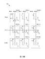
記憶體陣列200包含以欄-列配置佈置的多個記憶體單元。舉例而言,記憶體陣列200包含多個記憶體單元(例如200-1、200-2、200-3、200-4、200-5、200-6、 200-7、200-8、200-9等),每個欄有一條位元線(bit line, BL)以及一條第二字元線,每個列有一條字元線(word line, WL)。每個欄的位元線以及第二字元線分別耦接至多個位於此欄上的記憶體單元,且此欄的記憶體單元分別位於不同的列,並耦接至不同的字元線。亦即,每個記憶體陣列200上的記憶體單元耦接至一個欄上的一條位元線與一條第二字元線,以及一個列上的一條字元線。在一些實施例中,多條位元線與多條第二字元線會以縱向平行的方式排列,而多條字元線會以橫向平行的方式排列(即與位元線垂直)。接下來將以第3圖至第6圖為參考來討論進一步的細節。
參照第2圖更進一步的細節,出自於說明目的,在記憶體陣列200中列出了九個記憶體單元(例如200-1、200-2、200-3、200-4、200-5、200-6、200-7、200-8、200-9等)。基於以上描述,在記憶體陣列200中列出了相對應的欄A、B、C以及列a、b、c。記憶體單元200-1、200-4、200-7沿著欄A排列;記憶體單元200-2、200-5、200-8沿著欄B排列;記憶體單元200-3、200-6、200-9沿著欄C排列;記憶體單元200-1、200-2、200-3沿著列a排列;記憶體單元200-4、200-5、200-6沿著列b排列;記憶體單元200-7、200-8、200-9沿著列c排列。此外,沿著欄A排列的記憶體單元200-1、200-4、200-7皆耦接至一條欄A上的位元線BL_A,沿著欄A排列的記憶體單元200-1、200-4、200-7皆耦接至一條欄A上的第二字元線SWL_A,沿著欄A排列的記憶體單元200-1、200-4、200-7分別耦接至各自列的一條字元線:WL_a、WL_b以及WL_c;沿著欄B排列的記憶體單元200-2、200-5、200-8皆耦接至一條欄B上的位元線BL_B,沿著欄B排列的記憶體單元200-2、200-5、200-8皆耦接至一條欄B上的第二字元線SWL_B,沿著欄B排列的記憶體單元200-2、200-5、200-8分別耦接至各自列的一條字元線:WL_a、WL_b以及WL_c;沿著欄C排列的記憶體單元200-3、200-6、200-9皆耦接至一條欄C上的位元線BL_C,沿著欄C排列的記憶體單元200-3、200-6、200-9皆耦接至一條欄C上的第二字元線SWL_C,沿著欄C排列的記憶體單元200-3、200-6、200-9分別耦接至各自列的一條字元線:WL_a、WL_b以及WL_c。Referring to FIG. 2 for further details, nine memory cells (e.g., 200-1, 200-2, 200-3, 200-4, 200-5, 200-4, 200-5, 200-6, 200-7, 200-8, 200-9, etc.). Based on the above description, the corresponding columns A, B, C and columns a, b, c are listed in the
每個記憶體陣列200中的記憶體單元皆被配置為一個資料位元或是一個基準。這樣的資料位元可以從具有各自邏輯狀態的每個位元單元重複讀出或寫入(例如一個邏輯1或是一個邏輯0)。雖然第2圖示出了記憶體陣列200中的九個記憶體單元,任何期望數量的記憶體單元可以被包含在記憶體陣列200中,同時保持在本揭示文件的範圍內。如此一來,欄數與列數(以及對應的位元線與字元線)可以根據記憶體陣列200中的記憶體單元的數量進行調整。Each memory cell in the
根據本揭示文件的各種實施例,字元線解碼器202是提供電壓或電流的電路,將其提供至記憶體陣列200的一條或多條字元線。另一方面,位元線解碼器204是提供電壓或電流的電路,將其提供至記憶體陣列200的一條或多條位元線(以及在數個實施例中,一條或多條第二字元線)。在一些實施例中,位元線解碼器204會耦接至或嵌入一個耦接至記憶體陣列200的位元線控制器214。在一些實施例中,位元線控制器214可以偵測從記憶體陣列200至一條或多條位元線的電壓或電流。According to various embodiments of the present disclosure,
在一個示例中,為了將資料寫入記憶體單元200-1,字元線解碼器202從連接至記憶體單元200-1的字元線(在一些實施例中,從連接至記憶體單元200-1的第二位元線)施加電壓或電流至記憶體單元200-1,而位元線解碼器204從連接至記憶體單元200-1的位元線(在一些實施例中,從連接至記憶體單元200-1的第二字元線)施加電壓或電流至記憶體單元200-1。在一個示例中,為了從記憶體單元200-1讀取資料,字元線解碼器202從連接至記憶體單元200-1的字元線施加電壓或電流至記憶體單元200-1,而位元線控制器214從連接至記憶體單元200-1的位元線偵測記憶體單元200-1的記憶體資料所對應的電壓或電流。在一些實施例中,記憶體系統20包含更多、更少,或是不同於第1圖所示之組件。In one example, in order to write data into the memory unit 200-1, the
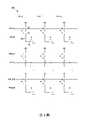
第3圖根據一些實施例繪示用於記憶體陣列(例如記憶體裝置)的方塊圖。在一些實施例中,記憶體陣列300除了揭示更多細節之外,與記憶體陣列200相似。詳細而言,記憶體陣列300揭示了每個記憶體單元的子組件。在一些實施例中,記憶體陣列300包含可以以欄-列配置佈置(例如M個列嶼N個欄)的多個記憶體單元。舉例而言,記憶體陣列300包含多個記憶體單元(例如MC(0,0)、MC(1,0)、MC(M,0)、MC(0,1)、MC(1,1)、MC(M,1)、MC(0,N)、MC(1,N)、MC(M,N)等),每個欄有一條位元線(BL)以及一條第二字元線(SWL),每個列有一條字元線(WL)。每個欄的位元線以及第二字元線分別耦接至多個位於此欄上的記憶體單元,且此欄的記憶體單元分別位於不同的列,並耦接至不同的字元線。同樣地,每個列的字元線分別耦接至多個位於此列上的記憶體單元,且此列的記憶體單元分別位於不同的欄,並耦接至不同的位元線及不同的第二字元線。在一些實施例中,多個記憶體單元中的每個記憶體單元(例如MC(0,0))皆相似於第2圖之多個記憶體單元中對應的記憶體單元(例如200-1)。FIG. 3 illustrates a block diagram for a memory array (eg, a memory device) according to some embodiments. In some embodiments,
參照第3圖更進一步的細節,出自於說明目的,在記憶體陣列300中列出了九個記憶體單元(例如MC(0,0)、MC(1,0)、MC(M,0)、MC(0,1)、MC(1,1)、MC(M,1)、MC(0,N)、MC(1,N)、MC(M,N))。記憶體單元MC(0,0)、MC(1,0)、MC(M,0)沿著第一欄排列並耦接至位元線BL(0)及第二字元線SWL(0);記憶體單元MC(0,1)、MC(1,1)、MC(M,1)沿著第二欄排列並耦接至位元線BL(1)及第二字元線SWL(1);記憶體單元MC(0,N)、MC(1,N)、MC(M,N)沿著第三欄排列並耦接至位元線BL(N)及第二字元線SWL(N);記憶體單元MC(0,0)、MC(0,1)、MC(0,N)沿著第一列排列並耦接至字元線WL(0);記憶體單元MC(1,0)、MC(1,1)、MC(1,N)沿著第二列排列並耦接至字元線WL(1);記憶體單元MC(M,0)、MC(M,1)、MC(M,N)沿著第三列排列並耦接至字元線WL(M)。Referring to FIG. 3 for further details, for illustrative purposes, nine memory cells (e.g., MC(0,0), MC(1,0), MC(M,0) are listed in
如第3圖所展示,每個記憶體單元包含第一電晶體M1、第二電晶體M2、記憶體元件(例如電阻)R1以及一個第三電晶體M3,第二電晶體M2耦接至第一電晶體M1,記憶體元件(例如電阻)R1耦接至第二電晶體M2,第三電晶體M3耦接至記憶體元件R1。其中每個記憶體單元對應的字元線耦接至第一電晶體M1,第二字元線耦接至第二電晶體M2,而位元線耦接至第三電晶體M3。舉例而言,記憶體單元MC(0,0)包含第一電晶體M1,第二電晶體M2耦接至第一電晶體M1,記憶體元件R1耦接至第二電晶體M2,以及第三電晶體M3耦接至記憶體元件R1。具體而言,在一些實施例中,第一電晶體M1的汲極耦接至第二電晶體M2的源極,第二電晶體M2的汲極耦接至記憶體元件R1的其中一端,而記憶體元件R1的另外一端耦接至第三電晶體M3的汲極。更進一步舉例,字元線WL(0)耦接至第一電晶體M1,第二字元線SWL(0)耦接至第二電晶體M2,而位元線BL(0)耦接至第三電晶體M3。具體而言,在一些實施例中,字元線WL(0)耦接至第一電晶體M1的閘極,第二字元線SWL(0)耦接至第二電晶體M2的閘極,而位元線BL(0)耦接至第三電晶體M3的閘極。第一電晶體M1可以稱為共源電晶體,第二電晶體M2可以稱為共源共柵電晶體。第一電晶體M1與第二電晶體M2可以統稱為堆疊存取電晶體。As shown in FIG. 3, each memory cell includes a first transistor M1, a second transistor M2, a memory element (such as a resistor) R1 and a third transistor M3, and the second transistor M2 is coupled to the second transistor M3. A transistor M1, a memory element (such as a resistor) R1 is coupled to the second transistor M2, and a third transistor M3 is coupled to the memory element R1. The word line corresponding to each memory cell is coupled to the first transistor M1, the second word line is coupled to the second transistor M2, and the bit line is coupled to the third transistor M3. For example, the memory unit MC(0,0) includes a first transistor M1, a second transistor M2 coupled to the first transistor M1, a memory element R1 coupled to the second transistor M2, and a third transistor M2 The transistor M3 is coupled to the memory element R1. Specifically, in some embodiments, the drain of the first transistor M1 is coupled to the source of the second transistor M2, the drain of the second transistor M2 is coupled to one end of the memory element R1, and The other end of the memory element R1 is coupled to the drain of the third transistor M3. As a further example, the word line WL(0) is coupled to the first transistor M1, the second word line SWL(0) is coupled to the second transistor M2, and the bit line BL(0) is coupled to the second transistor M2. Three-transistor M3. Specifically, in some embodiments, the word line WL(0) is coupled to the gate of the first transistor M1, and the second word line SWL(0) is coupled to the gate of the second transistor M2, And the bit line BL(0) is coupled to the gate of the third transistor M3. The first transistor M1 may be called a cascode transistor, and the second transistor M2 may be called a cascode transistor. The first transistor M1 and the second transistor M2 may be collectively referred to as stacked access transistors.
如第3圖所展示,第一電晶體M1與第二電晶體M2皆為一N型金屬氧化半導體電晶體,而第三電晶體M3為一P型金屬氧化半導體電晶體。然而,在一些實施例中,第一電晶體M1與第二電晶體M2皆為一P型金屬氧化半導體電晶體,而第三電晶體M3為一N型金屬氧化半導體電晶體。第一電晶體M1、第二電晶體M2、第三電晶體M3可以是其他各種電晶體類型中的任何一種,同時仍在本揭示文件的範圍內。第一電晶體M1、第二電晶體M2、第三電晶體M3可以具有標準臨界電壓(standard threshold voltage , SVT)、低臨界電壓(low threshold voltage , LVT)、高臨界電壓(high threshold voltage , HVT)、高電壓(high voltage , HV)、輸入/輸出(input/output , IO)或任何其他各種MOS器件類型。As shown in FIG. 3 , both the first transistor M1 and the second transistor M2 are N-type MOS transistors, and the third transistor M3 is a P-type MOS transistor. However, in some embodiments, both the first transistor M1 and the second transistor M2 are P-type MOS transistors, and the third transistor M3 is an N-type MOS transistor. The first transistor M1, the second transistor M2, and the third transistor M3 may be any of various other transistor types while remaining within the scope of the present disclosure. The first transistor M1, the second transistor M2, and the third transistor M3 may have a standard threshold voltage (standard threshold voltage, SVT), a low threshold voltage (low threshold voltage, LVT), a high threshold voltage (high threshold voltage, HVT) ), high voltage (high voltage, HV), input/output (input/output, IO) or any other various MOS device types.
第一電晶體M1(例如第一電晶體M1的源極)耦接至第一參考線,而第三電晶體M3(例如第三電晶體M3的源極)至第二參考線。如第3圖所示,第一電晶體M1耦接至地線(例如地線提供帶有0伏特的第一個訊號),第三電晶體M3耦接至電源供應線(例如電源供應線提供帶有電源供應器之電壓的第二個訊號)。然而,在一些實施例中,第一電晶體M1耦接至電源供應線,而第三電晶體M3耦接至地線。第一電晶體M1與第三電晶體M3可以耦接至其他各種參考線類型中的任何一種,同時仍在本揭示文件的範圍內。The first transistor M1 (eg, the source of the first transistor M1 ) is coupled to the first reference line, and the third transistor M3 (eg, the source of the third transistor M3 ) is coupled to the second reference line. As shown in Figure 3, the first transistor M1 is coupled to the ground (for example, the ground provides the first signal with 0 volts), and the third transistor M3 is coupled to the power supply line (for example, the power supply line provides second signal with the voltage of the power supply). However, in some embodiments, the first transistor M1 is coupled to the power supply line, and the third transistor M3 is coupled to the ground line. The first transistor M1 and the third transistor M3 may be coupled to any of various other reference line types while remaining within the scope of the present disclosure.
如圖3所示,記憶體元件為一個電阻(例如一個電子可程式熔絲電阻)。然而,此記憶體元件可以是一個憶阻器、一個電容、一個電感,或是其他各種記憶體元件類型中的任何一種,同時仍在本揭示文件的範圍內。As shown in FIG. 3, the memory element is a resistor (such as an electronic programmable fuse resistor). However, the memory element may be a memristor, a capacitor, an inductor, or any of various other memory element types while remaining within the scope of the present disclosure.
在一些實施例中,寫入的操作是藉由第一電晶體M1接收一個字元線的訊號、第二電晶體M2接收一個第二字元線的訊號,以及第三電晶體M3接收一個位元線的訊號。寫入操作的結果,會使得記憶體元件R1的狀態(例如電阻值)改變。在一些實施例中,讀取的操作是藉由第一電晶體M1接收一個字元線的訊號、第二電晶體M2接收一個第二字元線的訊號,以及第三電晶體M3傳送一個位元線的訊號。記憶體元件R1的狀態可以以位元線訊號的電壓(或電流)值為基準所決定。在一些實施例中,記憶體陣列300的運作與記憶體陣列200相同。In some embodiments, the write operation is performed by the first transistor M1 receiving a word line signal, the second transistor M2 receiving a second word line signal, and the third transistor M3 receiving a bit Yuan line signal. As a result of the write operation, the state (eg resistance value) of the memory element R1 will be changed. In some embodiments, the read operation is performed by the first transistor M1 receiving a word line signal, the second transistor M2 receiving a second word line signal, and the third transistor M3 transmitting a bit Yuan line signal. The state of the memory element R1 can be determined based on the voltage (or current) value of the bit line signal. In some embodiments,
第4圖根據一些實施例繪示用於記憶體陣列(例如記憶體裝置)的方塊圖。在一些實施例中,記憶體陣列400除了此處描述的差異之外,與記憶體陣列300相似。詳細而言,差異包含每個記憶體單元耦接至一條第二位元線,而非第二字元線。記憶體陣列400包含數個記憶體單元,其中每個欄有一條位元線(BL),每個列有一條字元線(WL)以及一條第二位元線(SBL)。在一些實施例中,記憶體陣列400會省略第二字元線。每個欄的位元線分別耦接至多個位於此欄上的記憶體單元,且此欄的記憶體單元分別位於不同的列,並耦接至不同的字元線以及不同的第二位元線。同樣地,每個列的字元線以及第二位元線分別耦接至多個位於此列上的記憶體單元,且此列的記憶體單元分別位於不同的欄,並耦接至不同的位元線。FIG. 4 shows a block diagram for a memory array (eg, a memory device), according to some embodiments. In some embodiments,
如第4圖所展示,每個記憶體單元包含一個第一電晶體M1,一個記憶體元件(例如電阻)R1耦接至第一電晶體M1,一個第二電晶體M4耦接至記憶體元件R1,以及一個第三電晶體M3耦接至第二電晶體M4。其中每個記憶體單元對應的字元線耦接至第一電晶體M1,第二位元線耦接至第二電晶體M4,而位元線耦接至第三電晶體M3。舉例而言,記憶體單元MC(0,0)包含第一電晶體M1,記憶體元件R1耦接至第一電晶體M1,第二電晶體M4耦接至記憶體元件R1,以及第三電晶體M3耦接至第二電晶體M4。具體而言,在一些實施例中,第一電晶體M1的汲極耦接至記憶體元件R1的其中一端,記憶體元件R1的另外一端耦接至第二電晶體M4的汲極,而第二電晶體M4的源極耦接至第三電晶體M3的汲極。更進一步舉例,字元線WL(0)耦接至第一電晶體M1,第二位元線SBL(0)耦接至第二電晶體M4,而位元線BL(0)耦接至第三電晶體M3。具體而言,在一些實施例中,字元線WL(0)耦接至第一電晶體M1的閘極,第二位元線SBL(0)耦接至第二電晶體M4的閘極,而位元線BL(0)耦接至第三電晶體M3的閘極。在一些實施例中,第一電晶體M1、第三電晶體M3、記憶體元件R1是第3圖的第一電晶體M1、第三電晶體M3、記憶體元件R1的實例。As shown in FIG. 4, each memory cell includes a first transistor M1, a memory element (such as a resistor) R1 is coupled to the first transistor M1, and a second transistor M4 is coupled to the memory element R1, and a third transistor M3 are coupled to the second transistor M4. The word line corresponding to each memory cell is coupled to the first transistor M1, the second bit line is coupled to the second transistor M4, and the bit line is coupled to the third transistor M3. For example, the memory unit MC(0,0) includes a first transistor M1, a memory element R1 is coupled to the first transistor M1, a second transistor M4 is coupled to the memory element R1, and a third transistor M4 is coupled to the memory element R1. The crystal M3 is coupled to the second transistor M4. Specifically, in some embodiments, the drain of the first transistor M1 is coupled to one end of the memory element R1, the other end of the memory element R1 is coupled to the drain of the second transistor M4, and the second transistor M4 The source of the second transistor M4 is coupled to the drain of the third transistor M3. As a further example, the word line WL(0) is coupled to the first transistor M1, the second bit line SBL(0) is coupled to the second transistor M4, and the bit line BL(0) is coupled to the second transistor M4. Three-transistor M3. Specifically, in some embodiments, the word line WL(0) is coupled to the gate of the first transistor M1, the second bit line SBL(0) is coupled to the gate of the second transistor M4, And the bit line BL(0) is coupled to the gate of the third transistor M3. In some embodiments, the first transistor M1, the third transistor M3, and the memory element R1 are examples of the first transistor M1, the third transistor M3, and the memory element R1 in FIG. 3 .
如第4圖所展示,第一電晶體M1為一N型金屬氧化半導體電晶體,而第二電晶體M4與第三電晶體M3皆為一P型金屬氧化半導體電晶體。然而,在一些實施例中,第一電晶體M1為一P型金屬氧化半導體電晶體,而第二電晶體M4與第三電晶體M3皆為一N型金屬氧化半導體電晶體。第一電晶體M1、第二電晶體M4、第三電晶體M3可以是其他各種電晶體類型中的任何一種,同時仍在本揭示文件的範圍內。第一電晶體M1、第二電晶體M4、第三電晶體M3可以具有標準臨界電壓、低臨界電壓、高臨界電壓、高電壓、輸入/輸出或任何其他各種MOS器件類型。As shown in FIG. 4 , the first transistor M1 is an N-type MOS transistor, and the second transistor M4 and the third transistor M3 are both a P-type MOS transistor. However, in some embodiments, the first transistor M1 is a P-type MOS transistor, and the second transistor M4 and the third transistor M3 are both an N-type MOS transistor. The first transistor M1, the second transistor M4, and the third transistor M3 may be any of various other transistor types while remaining within the scope of the present disclosure. The first transistor M1, the second transistor M4, and the third transistor M3 may have standard threshold voltage, low threshold voltage, high threshold voltage, high voltage, input/output or any other various MOS device types.
在一些實施例中,寫入的操作是藉由第一電晶體M1接收一個字元線的訊號、第三電晶體M3接收一個位元線的訊號,以及第二電晶體M4接收一個第二位元線的訊號。寫入操作的結果,會使得記憶體元件R1的狀態(例如電阻值)改變。在一些實施例中,讀取的操作是藉由第一電晶體M1接收一個字元線的訊號、第二電晶體M4接收一個第二位元線的訊號,以及第三電晶體M3傳送一個位元線的訊號。記憶體元件R1的狀態可以以位元線訊號的電壓(或電流)值為基準所決定。In some embodiments, the write operation is performed by the first transistor M1 receiving a word line signal, the third transistor M3 receiving a bit line signal, and the second transistor M4 receiving a second bit line Yuan line signal. As a result of the write operation, the state (eg resistance value) of the memory element R1 will be changed. In some embodiments, the read operation is performed by the first transistor M1 receiving a word line signal, the second transistor M4 receiving a second bit line signal, and the third transistor M3 transmitting a bit line. Yuan line signal. The state of the memory element R1 can be determined based on the voltage (or current) value of the bit line signal.
第5圖根據一些實施例繪示用於記憶體陣列(例如記憶體裝置)的方塊圖。在一些實施例中,記憶體陣列500除了此處描述的差異之外,與記憶體陣列300相似。詳細而言,差異包含每個記憶體單元耦接至多個第二字元線與多個第二位元線。記憶體陣列500包含數個記憶體單元,其中每個欄有一條位元線(BL)以及多條第二字元線(SWL0至SWLj-2),每個列有一條字元線(WL)以及多條第二位元線(SBL0至SBLi-2)。每個欄的位元線與第二字元線分別耦接至多個位於此欄上的記憶體單元,且此欄的記憶體單元分別位於不同的列,並耦接至不同的字元線以及不同的第二位元線。同樣地,每個列的字元線以及第二位元線分別耦接至多個位於此列上的記憶體單元,且此列的記憶體單元分別位於不同的欄,並耦接至不同的位元線與第二字元線。FIG. 5 shows a block diagram for a memory array (eg, a memory device) according to some embodiments. In some embodiments,
如第5圖所示,每個記憶體單元包含j個電晶體(M1、MSWL0……MSWLj-2)以串聯的方式耦接,一個記憶體元件(例如電阻)ME1耦接至電晶體MSWLj-2,以及i個電晶體(M3、MSBL0……MSBLi-2)以串聯的方式耦接,且電晶體MSBLi-2耦接至記憶體元件。每個記憶體單元之中,對應的字元線耦接至電晶體M1,數個對應的第二字元線耦接至剩下的j-1個電晶體(MSWL0……MSWLj-2),對應的位元線耦接至電晶體M3,數個對應的第二位元線耦接至剩下的i-1個電晶體(MSBL0……MSBLi-2)。As shown in Figure 5, each memory cell contains j transistors (M1,
舉例而言,記憶體單元MC(0,0)包含電晶體M1,電晶體MSWL0耦接至電晶體M1,電晶體MSWLj-2耦接至電晶體MSWL0,一個記憶體元件(例如電阻)ME1耦接至電晶體MSWLj-2,電晶體MSBLi-2耦接至記憶體元件ME1,電晶體MSBL0耦接至電晶體MSBLi-2,以及電晶體M3耦接至電晶體MSBL0。具體而言,在一些實施例中,電晶體M1的汲極耦接至電晶體MSWL0的源極,電晶體MSWL0的汲極耦接至電晶體MSWLj-2的源極,電晶體MSWLj-2的汲極耦接至記憶體元件ME1的其中一端,記憶體元件ME1的另外一端耦接至電晶體MSBLi-2的汲極,電晶體MSBLi-2的源極耦接至電晶體MSBL0的汲極,而電晶體MSBL0的源極耦接至電晶體M3的汲極。For example, memory cell MC(0,0) includes transistor M1,
更進一步舉例,字元線WL(0)耦接至電晶體M1,第二字元線SWL0(0)耦接至電晶體MSWL0,第二字元線SWLj-2(0)耦接至電晶體MSWLj-2,第二位元線SBLi-2(0)耦接至電晶體MSBLi-2,第二位元線SBL0(0)耦接至電晶體MSBL0,而位元線BL(0)耦接至電晶體M3。具體而言,在一些實施例中,字元線WL(0)耦接至電晶體M1的閘極,第二字元線SWL0(0)耦接至電晶體MSWL0的閘極,第二字元線SWLj-2(0)耦接至電晶體MSWLj-2的閘極,第二位元線SBLi-2(0)耦接至電晶體MSBLi-2的閘極,第二位元線SBL0(0)耦接至電晶體MSBL0的閘極,而位元線BL(0)耦接至電晶體M3的閘極。在一些實施例中,電晶體M1、電晶體M3、記憶體元件ME1是第3圖的電晶體M1、電晶體M3、記憶體元件R1的實例。As a further example, the word line WL(0) is coupled to the transistor M1, the second word line SWL0 (0) is coupled to the
如第5圖所展示,電晶體M1、電晶體MSWL0、電晶體MSWLj-2皆為一N型金屬氧化半導體電晶體,而電晶體MSBL0、電晶體MSBLi-2、電晶體M3皆為一P型金屬氧化半導體電晶體。然而,在一些實施例中,電晶體M1、電晶體MSWL0、電晶體MSWLj-2皆為一P型金屬氧化半導體電晶體,而電晶體MSBL0、電晶體MSBLi-2、電晶體M3皆為一N型金屬氧化半導體電晶體。電晶體M1、電晶體MSWL0、電晶體MSWLj-2、電晶體MSBL0、電晶體MSBLi-2、電晶體M3可以是其他各種電晶體類型中的任何一種,同時仍在本揭示文件的範圍內。電晶體M1、電晶體MSWL0、電晶體MSWLj-2、電晶體MSBL0、電晶體MSBLi-2、電晶體M3可以具有標準臨界電壓、低臨界電壓、高臨界電壓、高電壓、輸入/輸出或任何其他各種MOS器件類型。As shown in FIG. 5, the transistor M1, the
在一些實施例中,寫入的操作是藉由電晶體M1接收一個字元線的訊號、電晶體MSWL0……電晶體MSWLj-2各自接收一個第二字元線的訊號、電晶體M3接收一個位元線的訊號,以及電晶體MSBL0……電晶體MSBLi-2各自接收一個第二位元線的訊號。寫入操作的結果,會使得記憶體元件ME1的狀態(例如電阻值)改變。在一些實施例中,讀取的操作是藉由電晶體M1接收一個字元線的訊號、電晶體MSWL0……電晶體MSWLj-2各自接收一個第二字元線的訊號、電晶體MSBL0……電晶體MSBLi-2各自接收一個第二位元線的訊號,以及電晶體M3傳送一個位元線的訊號。記憶體元件ME1的狀態可以以位元線訊號的電壓(或電流)值為基準所決定。In some embodiments, the writing operation is performed by transistor M1 receiving a signal of a word line,
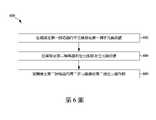
第6圖根據一些實施例繪示用於操作記憶體裝置的方法600之流程圖。應注意,方法600僅透過示例的方式提供並且不限制本揭示文件的範圍。因此,應理解,可以在第6圖的方法600之前、期間和之後提供額外的操作,而一些其他的操作可能在這裡只簡要描述。在一些實施例中,方法600由一個記憶體陣列(例如記憶體陣列200、記憶體陣列300、記憶體陣列400或記憶體陣列500)所實行。在一些實施例中,方法600的操作可以與第1圖至第5圖的記憶體裝置有所關聯。FIG. 6 shows a flowchart of a
方法600開始於操作602,從耦接至第一解碼器(例如字元線解碼器202)的字元線(例如WL(0))接收第一個字元線訊號。方法600接著實行操作604,從耦接至第二解碼器(例如位元線解碼器204)的位元線(例如BL(0))接收位元線訊號。在一些實施例中,方法600接著實行操作606,從耦接至第二解碼器的第二字元線(例如SWL(0))接收第二個位元線訊號。
在本揭示文件的一些態樣中,揭露一種記憶體裝置。在一些態樣中,記憶體裝置包含多個記憶體單元、多條字元線、多條位元線以及多條第二字元線。多個記憶體單元排列於多個欄以及多個列。多條字元線各自耦接至相對應之一列上的記憶體單元。多條位元線各自耦接至相對應之一欄上的記憶體單元。多條第二字元線各自耦接至相對應之一欄上的記憶體單元。In some aspects of this disclosure, a memory device is disclosed. In some aspects, a memory device includes a plurality of memory cells, a plurality of word lines, a plurality of bit lines, and a plurality of second word lines. Multiple memory units are arranged in multiple columns and multiple columns. Each of the word lines is coupled to memory cells on a corresponding column. A plurality of bit lines are respectively coupled to memory cells on a corresponding column. Each of the plurality of second word lines is coupled to the memory cells on a corresponding column.
在一些態樣中,位元線以及第二字元線耦接至一個相同的解碼器。在一些態樣中,記憶體裝置進一步包含多條第二位元線,第二位元線各自耦接至相對應之列上的記憶體單元。在一些態樣中,記憶體裝置進一步包含多條第三字元線,第三字元線各自耦接至相對應之欄上的記憶體單元。In some aspects, the bit line and the second word line are coupled to a same decoder. In some aspects, the memory device further includes a plurality of second bit lines, each of the second bit lines is coupled to the memory cells on the corresponding column. In some aspects, the memory device further includes a plurality of third word lines, each of which is coupled to the memory cells on the corresponding column.
在一些態樣中,記憶體單元各自包含一個第一金屬氧化半導體電晶體、一個第二金屬氧化半導體電晶體、一個記憶體元件以及一個第三金屬氧化半導體電晶體。第一金屬氧化半導體電晶體耦接至一條對應的字元線。第二金屬氧化半導體電晶體耦接至第一金屬氧化半導體電晶體以及一條對應的第二字元線。記憶體元件耦接至第二金屬氧化半導體電晶體。第三金屬氧化半導體電晶體耦接至記憶體元件以及一條對應的位元線。在一些態樣中,記憶體元件為一個電阻。In some aspects, the memory cells each include a first MOS transistor, a second MOS transistor, a memory element, and a third MOS transistor. The first MOS transistor is coupled to a corresponding word line. The second MOS transistor is coupled to the first MOS transistor and a corresponding second word line. The memory element is coupled to the second MOS transistor. The third MOS transistor is coupled to the memory device and a corresponding bit line. In some aspects, the memory element is a resistor.
在一些態樣中,第一金屬氧化半導體電晶體及第二金屬氧化半導體電晶體為N型金屬氧化半導體電晶體,且第三金屬氧化半導體電晶體為P型金屬氧化半導體電晶體。在一些態樣中,第一金屬氧化半導體電晶體及第二金屬氧化半導體電晶體為P型金屬氧化半導體電晶體,且第三金屬氧化半導體電晶體為N型金屬氧化半導體電晶體。在一些態樣中,記憶體單元進一步包含一個第四金屬氧化半導體電晶體,耦接於第三金屬氧化半導體電晶體及記憶體元件之間,且第四金屬氧化半導體電晶體耦接至一條對應的第二位元線。在一些態樣中,記憶體單元進一步包含一個第四金屬氧化半導體電晶體,耦接於第二金屬氧化半導體電晶體及記憶體元件之間,且第四金屬氧化半導體電晶體耦接至一條對應的第三字元線。In some aspects, the first MOS transistor and the second MOS transistor are N-type MOS transistors, and the third MOS transistor is a P-type MOS transistor. In some aspects, the first MOS transistor and the second MOS transistor are P-type MOS transistors, and the third MOS transistor is an N-type MOS transistor. In some aspects, the memory cell further includes a fourth MOS transistor coupled between the third MOS transistor and the memory element, and the fourth MOS transistor is coupled to a corresponding the second bit line. In some aspects, the memory cell further includes a fourth MOS transistor coupled between the second MOS transistor and the memory element, and the fourth MOS transistor is coupled to a corresponding The third character line of the .
在本揭示文件的一些態樣中,揭露一種記憶體系統。在一些態樣中,記憶體系統包含多個記憶體單元以及一個解碼器。記憶體單元各自耦接至一條字元線、一條位元線以及一條第二字元線。解碼器耦接至記憶體單元各自對應的位元線以及記憶體單元各自對應的第二字元線。In some aspects of this disclosure, a memory system is disclosed. In some aspects, the memory system includes multiple memory units and a decoder. The memory cells are respectively coupled to a word line, a bit line and a second word line. The decoders are coupled to respective bit lines corresponding to the memory units and to respective second word lines corresponding to the memory units.
在一些態樣中,記憶體單元排列於多個欄以及多個列。這些列的記憶體單元耦接至一條對應的位元線。這些欄的記憶體單元耦接至一條對應的第二字元線。在一些態樣中,這些列的記憶體單元耦接至一條對應的第二位元線。在一些態樣中,這些欄的記憶體單元耦接至一條對應的第三字元線。In some aspects, memory cells are arranged in multiple columns and multiple columns. The memory cells of the columns are coupled to a corresponding bit line. The columns of memory cells are coupled to a corresponding second word line. In some aspects, the columns of memory cells are coupled to a corresponding second bit line. In some aspects, the columns of memory cells are coupled to a corresponding third word line.
在一些態樣中,記憶體單元包含一個第一金屬氧化半導體電晶體、一個第二金屬氧化半導體電晶體、一個記憶體元件以及一個第三金屬氧化半導體電晶體。第一金屬氧化半導體電晶體耦接至一條對應的字元線。第二金屬氧化半導體電晶體耦接至第一金屬氧化半導體電晶體以及一條對應的字元線。記憶體元件耦接至第二金屬氧化半導體電晶體。第三金屬氧化半導體電晶體耦接至記憶體元件以及一條對應的位元線。在一些態樣中,該記憶體元件為一個電阻。In some aspects, the memory cell includes a first MOS transistor, a second MOS transistor, a memory element, and a third MOS transistor. The first MOS transistor is coupled to a corresponding word line. The second MOS transistor is coupled to the first MOS transistor and a corresponding word line. The memory element is coupled to the second MOS transistor. The third MOS transistor is coupled to the memory device and a corresponding bit line. In some aspects, the memory element is a resistor.
在一些態樣中,第一金屬氧化半導體電晶體及第二金屬氧化半導體電晶體為N型金屬氧化半導體電晶體,且第三金屬氧化半導體電晶體為P型金屬氧化半導體電晶體。在一些態樣中,第一金屬氧化半導體電晶體及第二金屬氧化半導體電晶體為P型金屬氧化半導體電晶體,且第三金屬氧化半導體電晶體為N型金屬氧化半導體電晶體。In some aspects, the first MOS transistor and the second MOS transistor are N-type MOS transistors, and the third MOS transistor is a P-type MOS transistor. In some aspects, the first MOS transistor and the second MOS transistor are P-type MOS transistors, and the third MOS transistor is an N-type MOS transistor.
在本揭示文件的一些態樣中,揭露一種操作記憶體裝置的方法。在一些態樣中,操作記憶體裝置的方法包含從耦接至第一解碼器的字元線接收字元線訊號。從耦接至第二解碼器的位元線接收位元線訊號。從耦接至第二解碼器的第二字元線接收第二字元線訊號。在一些態樣中,操作記憶體裝置的方法進一步包含從耦接至第一解碼器的第二位元線接收第二位元線訊號。In some aspects of the present disclosure, a method of operating a memory device is disclosed. In some aspects, a method of operating a memory device includes receiving a word line signal from a word line coupled to a first decoder. A bit line signal is received from a bit line coupled to the second decoder. A second word line signal is received from a second word line coupled to the second decoder. In some aspects, the method of operating a memory device further includes receiving a second bit line signal from a second bit line coupled to the first decoder.
前文概述了數個實施例的特徵,使得熟習此項技術者可更好地理解本案的態樣。熟習此項技術者應瞭解,可易於使用本案作為設計或修改其他製程及結構的基礎以便實施本文所介紹的實施例的相同目的及/或實現相同優勢。熟習此項技術者亦應認識到,此類等效結構並未脫離本案的精神及範疇,並且可在不脫離本案的精神及範疇的情況下在本文中實施各種變化、取代及修改。The foregoing outlines features of several embodiments so that those skilled in the art can better understand aspects of the present case. Those skilled in the art will appreciate that this disclosure can readily be used as a basis for designing or modifying other processes and structures in order to carry out the same purposes and/or achieve the same advantages of the embodiments described herein. Those skilled in the art should also realize that such equivalent constructions do not depart from the spirit and scope of the disclosure, and that various changes, substitutions and modifications can be made herein without departing from the spirit and scope of the disclosure.
100:積體電路 102:微處理器 104:隨機存取記憶體 106:唯讀記憶體 108:快取記憶體 110:系統控制 112:輸入/輸出介面 20:記憶體系統 200:記憶體陣列 200-1~200-9:記憶體單元 202:字元線解碼器 204:位元線解碼器 214:位元線控制器 BL_A、BL_B、BL_C:位元線 WL_a、WL_b、WL_c:字元線 SWL_a、SWL_b、SWL_c:第二字元線 300:記憶體陣列 BL(0)、BL(1)、BL(N):位元線 WL(0)、WL(1)、WL(M):字元線 SWL(0)、SWL(1)、SWL(N):第二字元線 MC(0,0)、MC(1,0)、MC(M,0):記憶體單元 MC(0,1)、MC(1,1)、MC(M,1):記憶體單元 MC(0,N)、MC(1,N)、MC(M,N):記憶體單元 M1~M3:金屬氧化半導體電晶體 R1:記憶體元件 400:記憶體陣列 500:記憶體陣列 SBL0(0)、SBL0(1)、SBL0(M):第二位元線 SBLi-2(0)、SBLi-2(1)、SBLi-2(M):第二位元線 SWL0(0)、SWL0(1)、SWL0(N):第二字元線 SWLj-2(0)、SWLj-2(1)、SWLj-2(N):第二字元線 MSWL0、MSBL0:金屬氧化半導體電晶體 MSWLj-2、MSBLi-2:金屬氧化半導體電晶體 ME1:記憶體元件 600:操作記憶體裝置之方法 602、604、606:操作100: integrated circuit 102: microprocessor 104: random access memory 106: read only memory 108: cache memory 110: system control 112: input/output interface 20: memory system 200: memory array 200 -1~200-9: memory unit 202: word line decoder 204: bit line decoder 214: bit line controller BL_A, BL_B, BL_C: bit line WL_a, WL_b, WL_c: word line SWL_a , SWL_b, SWL_c: second word line 300: memory array BL (0), BL (1), BL (N): bit line WL (0), WL (1), WL (M): character Line SWL(0), SWL(1), SWL(N): second word line MC(0,0), MC(1,0), MC(M,0): memory cell MC(0,1 ), MC(1,1), MC(M,1): memory unit MC(0,N), MC(1,N), MC(M,N): memory unit M1~M3: metal oxide semiconductor Transistor R1: memory element 400: memory array 500: memory array SBL0 (0), SBL0 (1), SBL0 (M): second bit line SBLi-2 (0), SBLi -2 (1), SBLi-2 (M): second bit line SWL0 (0), SWL0 (1), SWL0 (N): second word line SWLj-2 (0), SWLj-2 (1), SWLj-2 (N): second word line MSWL 0, MSBL 0: metal oxide semiconductor transistor MSWL j-2, MSBL i-2: metal oxide semiconductor transistor Crystal ME1: memory element 600: method of operating memory device 602, 604, 606: operation
當結合隨附圖式閱讀時,將自下文的詳細描述最佳地理解本案的態樣。應注意,根據工業中的標準實務,並未按比例繪製各特徵。事實上,為了論述清楚,可任意增加或減小各特徵的尺寸: 第1圖根據一些實施例繪示用於大規模積體電路的示例性方塊圖; 第2圖根據一些實施例繪示用於記憶體系統的方塊圖; 第3圖根據一些實施例繪示用於記憶體陣列的方塊圖; 第4圖根據一些實施例繪示用於另一個記憶體陣列的方塊圖; 第5圖根據一些實施例繪示用於再另一個記憶體陣列的方塊圖; 第6圖根據一些實施例繪示用於操作記憶體裝置的方法之流程圖。The aspects of the present case are best understood from the following detailed description when read in conjunction with the accompanying drawings. It should be noted that, in accordance with the standard practice in the industry, features are not drawn to scale. In fact, the dimensions of the various features can be arbitrarily increased or decreased for clarity of discussion: FIG. 1 illustrates an exemplary block diagram for a large scale integrated circuit, according to some embodiments; Figure 2 illustrates a block diagram for a memory system according to some embodiments; FIG. 3 illustrates a block diagram for a memory array, according to some embodiments; FIG. 4 illustrates a block diagram for another memory array, according to some embodiments; FIG. 5 illustrates a block diagram for yet another memory array, according to some embodiments; FIG. 6 illustrates a flowchart of a method for operating a memory device, according to some embodiments.
20:記憶體系統20: Memory system
200:記憶體陣列200: memory array
200-1~200-9:記憶體單元200-1~200-9: memory unit
202:字元線解碼器202: character line decoder
204:位元線解碼器204: bit line decoder
214:位元線控制器214: bit line controller
BL_A、BL_B、BL_C:位元線BL_A, BL_B, BL_C: bit lines
WL_a、WL_b、WL_c:字元線WL_a, WL_b, WL_c: word line
SWL_a、SWL_b、SWL_c:第二字元線SWL_a, SWL_b, SWL_c: second word line
Claims (20)
Translated fromChineseApplications Claiming Priority (2)
| Application Number | Priority Date | Filing Date | Title |
|---|---|---|---|
| US17/331,340US11763875B2 (en) | 2021-05-26 | 2021-05-26 | Second word line combined with Y-MUX signal in high voltage memory program |
| US17/331,340 | 2021-05-26 |
Publications (1)
| Publication Number | Publication Date |
|---|---|
| TW202247184Atrue TW202247184A (en) | 2022-12-01 |
Family
ID=83325292
Family Applications (1)
| Application Number | Title | Priority Date | Filing Date |
|---|---|---|---|
| TW110132524ATW202247184A (en) | 2021-05-26 | 2021-09-01 | Memory device |
Country Status (3)
| Country | Link |
|---|---|
| US (2) | US11763875B2 (en) |
| CN (1) | CN115116525A (en) |
| TW (1) | TW202247184A (en) |
Family Cites Families (15)
| Publication number | Priority date | Publication date | Assignee | Title |
|---|---|---|---|---|
| KR100534216B1 (en)* | 2004-06-18 | 2005-12-08 | 삼성전자주식회사 | Word line driver circuits for use in semiconductor memory and method for driving therefore |
| US7206247B2 (en)* | 2005-06-28 | 2007-04-17 | Cypress Semiconductor Corporation | Antifuse circuit with dynamic current limiter |
| US7206214B2 (en)* | 2005-08-05 | 2007-04-17 | Freescale Semiconductor, Inc. | One time programmable memory and method of operation |
| US7544968B1 (en)* | 2005-08-24 | 2009-06-09 | Xilinx, Inc. | Non-volatile memory cell with charge storage element and method of programming |
| JP4855851B2 (en)* | 2006-07-03 | 2012-01-18 | 株式会社東芝 | Semiconductor memory device |
| WO2008016948A2 (en) | 2006-07-31 | 2008-02-07 | Sandisk 3D Llc | Dual data-dependent busses for coupling read/write circuits to a memory array |
| WO2008088135A1 (en)* | 2007-01-16 | 2008-07-24 | Chungbuk National University Industry-Academic Cooperation Foundation | Multiple valued dynamic random access memory cell and thereof array using single electron transistor |
| KR20130032458A (en)* | 2011-09-23 | 2013-04-02 | 에스케이하이닉스 주식회사 | Semiconductor device with otp memory cell |
| KR102274259B1 (en)* | 2014-11-26 | 2021-07-07 | 삼성전자주식회사 | One-time programmable(otp) memory cell and otp memory device for multi-bit program |
| US9502426B1 (en)* | 2015-07-06 | 2016-11-22 | Ememory Technology Inc. | One time programming non-volatile memory cell |
| US10403338B2 (en)* | 2015-08-30 | 2019-09-03 | Chih-Cheng Hsiao | Low power memory device with column and row line switches for specific memory cells |
| US20160189755A1 (en)* | 2015-08-30 | 2016-06-30 | Chih-Cheng Hsiao | Low power memory device |
| US9620176B2 (en)* | 2015-09-10 | 2017-04-11 | Ememory Technology Inc. | One-time programmable memory array having small chip area |
| US9928886B2 (en)* | 2016-06-23 | 2018-03-27 | Chih-Cheng Hsiao | Low power memory device |
| US10777288B2 (en)* | 2018-08-07 | 2020-09-15 | Synopsys, Inc. | One time programmable (OTP) bit cell with integrated inhibit device |
- 2021
- 2021-05-26USUS17/331,340patent/US11763875B2/enactiveActive
- 2021-09-01TWTW110132524Apatent/TW202247184A/enunknown
- 2022
- 2022-01-11CNCN202210028486.4Apatent/CN115116525A/enactivePending
- 2023
- 2023-07-28USUS18/361,559patent/US12412620B2/enactiveActive
Also Published As
| Publication number | Publication date |
|---|---|
| US12412620B2 (en) | 2025-09-09 |
| CN115116525A (en) | 2022-09-27 |
| US20230377629A1 (en) | 2023-11-23 |
| US11763875B2 (en) | 2023-09-19 |
| US20220383934A1 (en) | 2022-12-01 |
Similar Documents
| Publication | Publication Date | Title |
|---|---|---|
| JP6205036B1 (en) | One-time programmable memory array with small chip area | |
| US8625339B2 (en) | Multi-cell per memory-bit circuit and method | |
| US9087572B2 (en) | Content addressable memory | |
| US10783976B2 (en) | Antifuse memory device and operation method thereof | |
| CN107636762A (en) | The disposable programmable memory realized using MRAM stack design | |
| KR20160062857A (en) | One-time programmable(otp) memory cell and otp memory device for multi-bit program | |
| US11328784B2 (en) | Memory with cells having multiple select transistors | |
| US9437274B1 (en) | Memory device | |
| US11915746B2 (en) | Memory device with word line pulse recovery | |
| US20070279967A1 (en) | High density magnetic memory cell layout for spin transfer torque magnetic memories utilizing donut shaped transistors | |
| US20250210074A1 (en) | Memory device and method of operating the same | |
| US20130039110A1 (en) | 3d architecture for bipolar memory using bipolar access device | |
| US20240386979A1 (en) | Bit Selection for Power Reduction in Stacking Structure During Memory Programming | |
| US11049549B2 (en) | Decoder structure including array of decoder cells organized into different rows | |
| CN110956993A (en) | Resistive memory cell based on resistive voltage divider reading | |
| TW202247184A (en) | Memory device | |
| CN106601300B (en) | Electric fuse storage unit, electric fuse storage array and using method thereof | |
| CN111028876B (en) | Non-volatile memory array for realizing bidirectional parallel data reading | |
| CN114496031A (en) | Memory device architecture using multiple cells per bit | |
| US12243599B2 (en) | Merged bit lines for high density memory array | |
| CN118412014B (en) | Storage unit, storage array, electronic device and data processing method | |
| US9214495B1 (en) | Memory cell structure and formation method thereof | |
| JP2015177126A (en) | semiconductor device |