TW202244873A - Pixel circuit and driving method thereof - Google Patents
Pixel circuit and driving method thereofDownload PDFInfo
- Publication number
- TW202244873A TW202244873ATW110116982ATW110116982ATW202244873ATW 202244873 ATW202244873 ATW 202244873ATW 110116982 ATW110116982 ATW 110116982ATW 110116982 ATW110116982 ATW 110116982ATW 202244873 ATW202244873 ATW 202244873A
- Authority
- TW
- Taiwan
- Prior art keywords
- transistor
- terminal
- control signal
- voltage
- coupled
- Prior art date
Links
- 238000000034methodMethods0.000titleclaimsdescription9
- 239000003990capacitorSubstances0.000claimsabstractdescription13
- 238000010586diagramMethods0.000description12
- 239000010409thin filmSubstances0.000description9
- 230000005540biological transmissionEffects0.000description5
- 239000011159matrix materialSubstances0.000description3
- 235000012431wafersNutrition0.000description3
- 239000013078crystalSubstances0.000description2
- 230000008878couplingEffects0.000description1
- 238000010168coupling processMethods0.000description1
- 238000005859coupling reactionMethods0.000description1
- 230000007423decreaseEffects0.000description1
- 238000005516engineering processMethods0.000description1
- 238000004519manufacturing processMethods0.000description1
- 239000000463materialSubstances0.000description1
- 238000012986modificationMethods0.000description1
- 230000004048modificationEffects0.000description1
- 229910021420polycrystalline siliconInorganic materials0.000description1
- 229920005591polysiliconPolymers0.000description1
- 239000004065semiconductorSubstances0.000description1
- 230000003068static effectEffects0.000description1
- 239000000758substrateSubstances0.000description1
Images


Classifications
- G—PHYSICS
- G09—EDUCATION; CRYPTOGRAPHY; DISPLAY; ADVERTISING; SEALS
- G09G—ARRANGEMENTS OR CIRCUITS FOR CONTROL OF INDICATING DEVICES USING STATIC MEANS TO PRESENT VARIABLE INFORMATION
- G09G3/00—Control arrangements or circuits, of interest only in connection with visual indicators other than cathode-ray tubes
- G09G3/20—Control arrangements or circuits, of interest only in connection with visual indicators other than cathode-ray tubes for presentation of an assembly of a number of characters, e.g. a page, by composing the assembly by combination of individual elements arranged in a matrix no fixed position being assigned to or needed to be assigned to the individual characters or partial characters
- G09G3/22—Control arrangements or circuits, of interest only in connection with visual indicators other than cathode-ray tubes for presentation of an assembly of a number of characters, e.g. a page, by composing the assembly by combination of individual elements arranged in a matrix no fixed position being assigned to or needed to be assigned to the individual characters or partial characters using controlled light sources
- G09G3/30—Control arrangements or circuits, of interest only in connection with visual indicators other than cathode-ray tubes for presentation of an assembly of a number of characters, e.g. a page, by composing the assembly by combination of individual elements arranged in a matrix no fixed position being assigned to or needed to be assigned to the individual characters or partial characters using controlled light sources using electroluminescent panels
- G09G3/32—Control arrangements or circuits, of interest only in connection with visual indicators other than cathode-ray tubes for presentation of an assembly of a number of characters, e.g. a page, by composing the assembly by combination of individual elements arranged in a matrix no fixed position being assigned to or needed to be assigned to the individual characters or partial characters using controlled light sources using electroluminescent panels semiconductive, e.g. using light-emitting diodes [LED]
- G09G3/3208—Control arrangements or circuits, of interest only in connection with visual indicators other than cathode-ray tubes for presentation of an assembly of a number of characters, e.g. a page, by composing the assembly by combination of individual elements arranged in a matrix no fixed position being assigned to or needed to be assigned to the individual characters or partial characters using controlled light sources using electroluminescent panels semiconductive, e.g. using light-emitting diodes [LED] organic, e.g. using organic light-emitting diodes [OLED]
- G09G3/3225—Control arrangements or circuits, of interest only in connection with visual indicators other than cathode-ray tubes for presentation of an assembly of a number of characters, e.g. a page, by composing the assembly by combination of individual elements arranged in a matrix no fixed position being assigned to or needed to be assigned to the individual characters or partial characters using controlled light sources using electroluminescent panels semiconductive, e.g. using light-emitting diodes [LED] organic, e.g. using organic light-emitting diodes [OLED] using an active matrix
- G09G3/3233—Control arrangements or circuits, of interest only in connection with visual indicators other than cathode-ray tubes for presentation of an assembly of a number of characters, e.g. a page, by composing the assembly by combination of individual elements arranged in a matrix no fixed position being assigned to or needed to be assigned to the individual characters or partial characters using controlled light sources using electroluminescent panels semiconductive, e.g. using light-emitting diodes [LED] organic, e.g. using organic light-emitting diodes [OLED] using an active matrix with pixel circuitry controlling the current through the light-emitting element
- G—PHYSICS
- G09—EDUCATION; CRYPTOGRAPHY; DISPLAY; ADVERTISING; SEALS
- G09G—ARRANGEMENTS OR CIRCUITS FOR CONTROL OF INDICATING DEVICES USING STATIC MEANS TO PRESENT VARIABLE INFORMATION
- G09G2300/00—Aspects of the constitution of display devices
- G09G2300/08—Active matrix structure, i.e. with use of active elements, inclusive of non-linear two terminal elements, in the pixels together with light emitting or modulating elements
- G09G2300/0809—Several active elements per pixel in active matrix panels
- G09G2300/0819—Several active elements per pixel in active matrix panels used for counteracting undesired variations, e.g. feedback or autozeroing
Landscapes
- Engineering & Computer Science (AREA)
- Physics & Mathematics (AREA)
- Computer Hardware Design (AREA)
- General Physics & Mathematics (AREA)
- Theoretical Computer Science (AREA)
- Electroluminescent Light Sources (AREA)
- Control Of Indicators Other Than Cathode Ray Tubes (AREA)
- Liquid Crystal Display Device Control (AREA)
- Control Of El Displays (AREA)
Abstract
Description
Translated fromChinese本揭示內容係有關於一種畫素電路及其驅動方法,特別是指一種適用於低畫面更新率的畫素電路及其驅動方法。The disclosure relates to a pixel circuit and its driving method, in particular to a pixel circuit and its driving method suitable for low frame update rate.
隨著數位顯示裝置的需求日益增加,低畫面更新率(或稱低幀率,Low Frame Rate)廣泛應用在顯示裝置中,用以降低電源消耗,達到省電、延長使用時間的目的。然而,在畫面未進行更新時,維持先前畫面的幀數在發光階段顯示的亮度會不穩定,將導致閃爍。With the increasing demand for digital display devices, low frame rate (or low frame rate, Low Frame Rate) is widely used in display devices to reduce power consumption, save power and prolong usage time. However, when the screen is not updated, the display brightness will be unstable during the light-emitting stage by maintaining the frame number of the previous screen, which will cause flickering.
本揭示內容的一態樣為一畫素電路。該畫素電路包括一驅動電晶體、一第一電晶體、一氧化物電晶體、一第二電晶體、一第三電晶體、一第四電晶體、一第五電晶體、一第六電晶體以及一電容。驅動電晶體的控制端耦接於一第一節點,該驅動電晶體的第一端接收一系統高電壓,且該驅動電晶體的第二端耦接於一第二節點。該第一電晶體的控制端接收一第一控制訊號,該第一電晶體的第一端耦接於一第三節點,且該第一電晶體的第二端耦接於該第二節點。該氧化物電晶體的控制端接收一第二控制訊號,該氧化物電晶體的第一端耦接於該第三節點,且該氧化物電晶體的第二端耦接於該第一節點。該第二電晶體的控制端接收一發光控制訊號,該第二電晶體的第一端耦接於一發光元件的陽極端,且該第二電晶體的第二端耦接於該第二節點。該第三電晶體的控制端接收一第三控制訊號,該第三電晶體的第一端耦接於該發光元件的陽極端,且該第三電晶體的第二端接收一第一參考電壓。該第四電晶體的控制端接收一第四控制訊號,該第四電晶體的第一端耦接於該第三節點,且該第四電晶體的第二端接收該第一參考電壓。該第五電晶體的控制端接收該第一控制訊號,該第五電晶體的第一端接收一資料電壓,且該第五電晶體的第二端耦接於一第四節點。該第六電晶體的控制端接收該發光控制訊號,該第六電晶體的第一端耦接於該第四節點,且該第六電晶體的第二端接收一第二參考電壓。該電容耦接於該第四節點以及該第一節點之間。One aspect of the disclosure is a pixel circuit. The pixel circuit includes a drive transistor, a first transistor, an oxide transistor, a second transistor, a third transistor, a fourth transistor, a fifth transistor, and a sixth transistor. crystal and a capacitor. The control terminal of the driving transistor is coupled to a first node, the first terminal of the driving transistor receives a system high voltage, and the second terminal of the driving transistor is coupled to a second node. The control terminal of the first transistor receives a first control signal, the first terminal of the first transistor is coupled to a third node, and the second terminal of the first transistor is coupled to the second node. The control terminal of the oxide transistor receives a second control signal, the first terminal of the oxide transistor is coupled to the third node, and the second terminal of the oxide transistor is coupled to the first node. The control terminal of the second transistor receives a light-emitting control signal, the first terminal of the second transistor is coupled to the anode terminal of a light-emitting element, and the second terminal of the second transistor is coupled to the second node . The control end of the third transistor receives a third control signal, the first end of the third transistor is coupled to the anode end of the light emitting element, and the second end of the third transistor receives a first reference voltage . The control terminal of the fourth transistor receives a fourth control signal, the first terminal of the fourth transistor is coupled to the third node, and the second terminal of the fourth transistor receives the first reference voltage. The control terminal of the fifth transistor receives the first control signal, the first terminal of the fifth transistor receives a data voltage, and the second terminal of the fifth transistor is coupled to a fourth node. The control terminal of the sixth transistor receives the light-emitting control signal, the first terminal of the sixth transistor is coupled to the fourth node, and the second terminal of the sixth transistor receives a second reference voltage. The capacitor is coupled between the fourth node and the first node.
本揭示內容的另一態樣為一驅動方法。該驅動方法適用於一畫素電路,包含:在一第一幀的一第一期間,重置一發光元件的陽極端至一第一參考電壓;在該第一幀的一第二期間,重置一驅動電晶體的控制端以及第二端至該第一參考電壓;在該第一幀的一第三期間,藉由導通一第一電晶體以及一氧化物電晶體提供一補償電壓至該驅動電晶體的控制端;以及在該第一幀的一第四期間,藉由導通的一第六電晶體以及一電容將一資料電壓耦合至該驅動電晶體的控制端,以使該驅動電晶體根據一工作電壓輸出一驅動電流至該發光元件。Another aspect of the disclosure is a driving method. The driving method is applicable to a pixel circuit, comprising: resetting the anode terminal of a light-emitting element to a first reference voltage during a first period of a first frame; and resetting during a second period of the first frame. setting a control terminal and a second terminal of a driving transistor to the first reference voltage; during a third period of the first frame, providing a compensation voltage to the first transistor by turning on a first transistor and an oxide transistor the control end of the drive transistor; and during a fourth period of the first frame, a data voltage is coupled to the control end of the drive transistor by means of a turned-on sixth transistor and a capacitor, so that the drive transistor The crystal outputs a driving current to the light emitting element according to an operating voltage.
綜上,在維持前一幀畫面訊號的期間中,本揭示不寫入新的資料電壓至畫素電路,但仍對發光元件的陽極端進行重置,使得發光元件不會有殘存的電荷影響發光亮度。藉由氧化物電晶體的設計,驅動電晶體的控制端的電壓準位較能保持與在進行畫面訊號更新的期間中相近的電壓準位。如此一來,便能在降低畫面更新率時(即在低幀數模式下),達到節省功耗並穩定發光亮度,避免產生閃爍的現象。To sum up, during the period of maintaining the picture signal of the previous frame, this disclosure does not write new data voltage to the pixel circuit, but still resets the anode terminal of the light-emitting element, so that the light-emitting element will not be affected by residual charges Luminous brightness. With the design of the oxide transistor, the voltage level of the control terminal of the driving transistor can maintain a voltage level close to that during the period of updating the picture signal. In this way, when the frame update rate is reduced (that is, in the low frame rate mode), power consumption can be saved and the brightness of the light can be stabilized to avoid flickering.
下文係舉實施例配合所附圖式作詳細說明,但所描述的具體實施例僅用以解釋本案,並不用來限定本案,而結構操作之描述非用以限制其執行之順序,任何由元件重新組合之結構,所產生具有均等功效的裝置,皆為本揭示內容所涵蓋的範圍。The following is a detailed description of the embodiments in conjunction with the accompanying drawings, but the described specific embodiments are only used to explain the present case, and are not used to limit the present case, and the description of the structure and operation is not used to limit the order of its execution. The recombined structure and the devices with equivalent functions are all within the scope of this disclosure.
在全篇說明書與申請專利範圍所使用之用詞(terms),除有特別註明外,通常具有每個用詞使用在此領域中、在此揭示之內容中與特殊內容中的平常意義。The terms (terms) used throughout the specification and claims, unless otherwise noted, generally have the ordinary meaning of each term used in this field, in the disclosed content and in the special content.
關於本文中所使用之「耦接」或「連接」,均可指二或多個元件相互直接作實體或電性接觸,或是相互間接作實體或電性接觸,亦可指二或多個元件相互操作或動作。As used herein, "coupling" or "connection" can refer to two or more components that are in direct physical or electrical contact with each other, or indirect physical or electrical contact with each other, and can also refer to two or more elements. Components operate or act on each other.
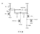
請參閱第1圖,第1圖描述根據本揭示的部分實施例所繪示的一畫素電路100。畫素電路100包括一驅動電晶體TD、一氧化物電晶體TO、複數個電晶體T1~T6、一電容C1以及一發光元件OLED。Please refer to FIG. 1 , which depicts a
於部分實施例中,畫素電路100可應用於顯示裝置。例如,主動式有機發光二極體顯示器(Active Matrix Organic Light Emitting Display,AMOLED)和主動式微發光二極體顯示器(Active Matrix Micro Light Emitting Display,AMOLED,AMµLED)等等。舉例來說,顯示裝置中可包含以陣列排列的多個畫素電路100,以組成完整的顯示面板。In some embodiments, the
於部分實施例中,除了多個畫素電路100以外,顯示裝置還可包含控制器、源極驅動器以及閘極驅動器。其中,控制器耦接源極驅動器與閘極驅動器,源極驅動器透過多個資料線連接至顯示面板中的多個畫素電路100,且閘極驅動器透過多個掃描線連接至顯示面板中的多個畫素電路100。控制器會藉由源極驅動器與閘極驅動器依序驅動每一列的畫素電路100。In some embodiments, in addition to the plurality of
如第1圖所示,驅動電晶體TD的控制端(例如閘極端)耦接於一節點N1,驅動電晶體TD的第一端(例如源極端)接收一系統高電壓OVDD,且驅動電晶體TD的第二端(例如汲極端)耦接於一節點N2。電晶體T1的第一端耦接於一節點N3,電晶體T1的第二端耦接於節點N2,且電晶體T1的控制端接收一第一控制訊號S2,使得電晶體T1用以根據第一控制訊號S2選擇性地導通或關斷。氧化物電晶體TO的第一端耦接於節點N3(即氧化物電晶體TO的第一端耦接於電晶體T1的第一端),氧化物電晶體TO的第二端耦接於節點N1(即氧化物電晶體TO的第二端耦接於驅動電晶體TD的控制端),且氧化物電晶體TO的控制端接收一第二控制訊號S3,使得氧化物電晶體TO用以根據第二控制訊號S3選擇性地導通或關斷。As shown in Figure 1, the control terminal (such as the gate terminal) of the driving transistor TD is coupled to a node N1, and the first terminal (such as the source terminal) of the driving transistor TD receives a system high voltage OVDD, and the driving transistor TD A second terminal (eg drain terminal) of TD is coupled to a node N2. The first terminal of the transistor T1 is coupled to a node N3, the second terminal of the transistor T1 is coupled to the node N2, and the control terminal of the transistor T1 receives a first control signal S2, so that the transistor T1 is used for controlling according to the first A control signal S2 is selectively turned on or off. The first end of the oxide transistor TO is coupled to the node N3 (that is, the first end of the oxide transistor TO is coupled to the first end of the transistor T1), and the second end of the oxide transistor TO is coupled to the node N1 (that is, the second terminal of the oxide transistor TO is coupled to the control terminal of the drive transistor TD), and the control terminal of the oxide transistor TO receives a second control signal S3, so that the oxide transistor TO is used according to The second control signal S3 is selectively turned on or off.
電晶體T2的第一端耦接於發光元件OLED的陽極端,且電晶體T2的第二端耦接於節點N2。換言之,驅動電晶體TD的第二端、電晶體T1的第二端以及電晶體T2的第二端耦接在一起。電晶體T2的控制端接收一發光控制訊號EM,使得電晶體T2用以根據發光控制訊號EM選擇性地導通或關斷。A first terminal of the transistor T2 is coupled to the anode terminal of the light emitting element OLED, and a second terminal of the transistor T2 is coupled to the node N2. In other words, the second terminal of the driving transistor TD, the second terminal of the transistor T1 and the second terminal of the transistor T2 are coupled together. The control terminal of the transistor T2 receives a light emission control signal EM, so that the transistor T2 is selectively turned on or off according to the light emission control signal EM.
電晶體T3的第一端耦接於發光元件OLED的陽極端(即電晶體T3的第一端耦接於電晶體T2的第一端),電晶體T3的第二端接收一參考電壓Vref_N,且電晶體T3的控制端接收一第三控制訊號S1[N],使得電晶體T3用以根據第三控制訊號S1[N]選擇性地導通或關斷。發光元件OLED的陰極端接收一系統低電壓OVSS。The first terminal of the transistor T3 is coupled to the anode terminal of the light-emitting element OLED (that is, the first terminal of the transistor T3 is coupled to the first terminal of the transistor T2), and the second terminal of the transistor T3 receives a reference voltage Vref_N, And the control terminal of the transistor T3 receives a third control signal S1 [N], so that the transistor T3 is selectively turned on or off according to the third control signal S1 [N]. The cathode terminal of the light emitting element OLED receives a system low voltage OVSS.
電晶體T4的第一端耦接於節點N3。換言之,電晶體T4的第一端、氧化物電晶體TO的第一端和電晶體T1的第一端耦接在一起。電晶體T4的第二端接收參考電壓Vref_N,且電晶體T4的控制端接收續傳級的第三控制訊號S1[N+1],使得電晶體T4用以根據續傳級的第三控制訊號S1[N+1]選擇性地導通或關斷。A first end of the transistor T4 is coupled to the node N3. In other words, the first terminal of the transistor T4, the first terminal of the oxide transistor TO and the first terminal of the transistor T1 are coupled together. The second end of the transistor T4 receives the reference voltage Vref_N, and the control end of the transistor T4 receives the third control signal S1[N+1] of the continuation stage, so that the transistor T4 is used to control the third control signal according to the continuation stage. S1[N+1] is selectively turned on or off.
電容C1耦接於節點N1以及一節點N4之間。電晶體T5的第一端接收一資料電壓Vdata,電晶體T5的第二端耦接於節點N4,且電晶體T5的控制端接收第一控制訊號S2,使得電晶體T5用以根據第一控制訊號S2選擇性地導通或關斷。電晶體T6的第一端耦接於節點N4(即電晶體T6的第一端耦接於電晶體T5的第二端),電晶體T6的第二端接收參考電壓Vref_P,且電晶體T6的控制端接收發光控制訊號EM,使得電晶體T6用以根據發光控制訊號EM選擇性地導通或關斷。The capacitor C1 is coupled between the node N1 and a node N4. The first end of the transistor T5 receives a data voltage Vdata, the second end of the transistor T5 is coupled to the node N4, and the control end of the transistor T5 receives the first control signal S2, so that the transistor T5 is used to The signal S2 is selectively turned on or off. The first end of the transistor T6 is coupled to the node N4 (that is, the first end of the transistor T6 is coupled to the second end of the transistor T5), the second end of the transistor T6 receives the reference voltage Vref_P, and the transistor T6 The control terminal receives the light emission control signal EM, so that the transistor T6 is selectively turned on or off according to the light emission control signal EM.
於部分實施例中,參考電壓Vref_P與參考電壓Vref_N具有相同的電壓準位,但本揭示並不以此為限。於其他實施例中,參考電壓Vref_P與參考電壓Vref_N分別具有不相同的電壓準位。值得注意的是,不管參考電壓Vref_P與參考電壓Vref_N是否具有相同的電壓準位,參考電壓Vref_P與參考電壓Vref_N皆分別由二個獨立的電壓源供應。In some embodiments, the reference voltage Vref_P and the reference voltage Vref_N have the same voltage level, but the disclosure is not limited thereto. In other embodiments, the reference voltage Vref_P and the reference voltage Vref_N have different voltage levels respectively. It should be noted that no matter whether the reference voltage Vref_P and the reference voltage Vref_N have the same voltage level or not, the reference voltage Vref_P and the reference voltage Vref_N are respectively supplied by two independent voltage sources.
於第1圖的實施例中,驅動電晶體TD以及電晶體T1~T6均為P型薄膜電晶體,而氧化物電晶體TO則為N型薄膜電晶體,但本揭示並不以此為限。於其他實施例中,驅動電晶體TD以及電晶體T1~T6均為N型薄膜電晶體,而氧化物電晶體TO受限於其製作材料的因素仍為N型薄膜電晶體。具體而言,驅動電晶體TD以及電晶體T1~T6的主動層主要是由多晶矽(poly silicon)形成,而氧化物電晶體TO的主動層主要是由氧化物半導體(oxide semiconductor)形成。In the embodiment shown in FIG. 1, the driving transistor TD and the transistors T1-T6 are all P-type thin film transistors, while the oxide transistor TO is an N-type thin film transistor, but the present disclosure is not limited thereto. . In other embodiments, the driving transistor TD and the transistors T1 - T6 are all N-type thin film transistors, while the oxide transistor TO is still an N-type thin film transistor due to its manufacturing material. Specifically, the active layers of the driving transistor TD and the transistors T1 - T6 are mainly formed of polysilicon, and the active layer of the oxide transistor TO is mainly formed of oxide semiconductor.
於部分實施例中,發光元件OLED可為有機發光二極體或微發光二極體等等。於部分實施例中,微發光二極體指的是二極體晶片尺寸在75μm以下,其中二極體晶片是先於二極體晶圓上生成,再透過巨量轉移技術轉移至顯示裝置的基板上以電性連接於電晶體。In some embodiments, the light emitting element OLED can be an organic light emitting diode or a micro light emitting diode, and the like. In some embodiments, micro light-emitting diodes refer to diode wafers with a size below 75 μm, wherein the diode wafers are first formed on the diode wafers, and then transferred to the display device through mass transfer technology The substrate is electrically connected to the transistor.
請參閱第2圖,第2圖為根據本揭示的部分實施例所繪示的第一控制訊號S2、第二控制訊號S3、第三控制訊號S1以及發光控制訊號EM的時序圖。於第2圖的實施例中,在一般模式下,畫素電路100的每一幀(frame)均如期間Fd所示。期間Fd中的訊號為一般進行畫面更新時的訊號。其中,第2圖中的第三控制訊號S1[N]代表用於控制第1圖中的畫素電路100的訊號,而第2圖中的續傳級的第三控制訊號S1[N+1]則代表用於驅動與畫素電路100相鄰的另一列的畫素電路的訊號。Please refer to FIG. 2 . FIG. 2 is a timing diagram of the first control signal S2 , the second control signal S3 , the third control signal S1 and the light emission control signal EM according to some embodiments of the present disclosure. In the embodiment of FIG. 2 , in the normal mode, each frame of the
接下來對畫素電路100的運作進行說明。如第2圖所示,期間Fd包括子期間P1~P4。具體而言,子期間P1為重置發光元件OLED的陽極端的階段,子期間P2為重置驅動電晶體TD的控制端與第二端的階段,子期間P3為畫素電路100的寫入和補償階段,而子期間P4為畫素電路100的發光階段。Next, the operation of the
請一併參閱第2及3A圖,第3A圖繪示在發光元件OLED的陽極端的重置階段(即子期間P1)中畫素電路100的各個電晶體的狀態示意圖。於子期間P1,第三控制訊號S1[N]切換至導通電壓準位(例如,對於P型薄膜電晶體而言為低電壓準位,對於N型薄膜電晶體而言為高電壓準位),且第一控制訊號S2、第二控制訊號S3、續傳級的第三控制訊號S1[N+1]與發光控制訊號EM則維持於關斷電壓準位(例如,對於P型薄膜電晶體而言為高電壓準位,而對於N型薄膜電晶體而言為低電壓準位)。如此一來,氧化物電晶體TO以及電晶體T1~T2和T4~T6均關斷,且電晶體T3導通,以提供參考電壓Vref_N至發光元件OLED的陽極端。據此,發光元件OLED的陽極端於子期間P1被重置至參考電壓Vref_N,以確保發光元件OLED的陽極端在發光階段(即子期間P4)前沒有殘留電荷。Please refer to FIGS. 2 and 3A together. FIG. 3A shows a schematic diagram of states of each transistor of the
請一併參閱第2及3B圖,第3B圖繪示在重置驅動電晶體TD的控制端與第二端的階段(即子期間P2)中畫素電路100的各個電晶體的狀態示意圖。於子期間P2,第三控制訊號S1[N]切換至關斷電壓準位,第一控制訊號S2、第二控制訊號S3與續傳級的第三控制訊號S1[N+1]切換至導通電壓準位,且發光控制訊號EM維持於關斷電壓準位。如此一來,電晶體T2、電晶體T3以及電晶體T6關斷,且電晶體T1、電晶體T4、電晶體T5以及氧化物電晶體TO導通,以將參考電壓Vref_N自電晶體T4的第二端提供至驅動電晶體TD的控制端(即節點N1)以及第二端(即節點N2)。據此,驅動電晶體TD的控制端以及第二端於子期間P2分別被重置至參考電壓Vref_N,從而能清除前一幀畫面的殘留電荷。Please refer to FIG. 2 and FIG. 3B together. FIG. 3B is a schematic diagram showing the state of each transistor of the
請一併參閱第2及3C圖,第3C圖繪示在寫入和補償階段(即子期間P3)中畫素電路100的各個電晶體的狀態示意圖。於子期間P3,續傳級的第三控制訊號S1[N+1]切換至關斷電壓準位,第一控制訊號S2與第二控制訊號S3維持於導通電壓準位,且第三控制訊號S1[N]與發光控制訊號EM維持於關斷電壓準位。如此一來,電晶體T2、電晶體T3、電晶體T4以及電晶體T6關斷,且電晶體T1、電晶體T5以及氧化物電晶體TO導通。此時,驅動電晶體TD的第一端和控制端的電壓差為系統高電壓OVDD減去參考電壓Vref_N。此電壓差大於驅動電晶體TD的一臨界電壓Vth,使得驅動電晶體TD導通。據此,導通後的驅動電晶體TD根據其第一端的系統高電壓OVDD對其控制端充電,直到驅動電晶體TD的第一端和控制端之間的電壓差減少至驅動電晶體TD的臨界電壓Vth。Please refer to FIG. 2 and FIG. 3C together. FIG. 3C is a schematic diagram showing the state of each transistor of the
也就是說,驅動電晶體TD的控制端(即節點N1)於子期間P3被補償至一補償電壓,此補償電壓即為系統高電壓OVDD減去驅動電晶體TD的臨界電壓Vth。此外,於子期間P3,資料電壓Vdata透過導通的電晶體T5被提供至節點N4。That is to say, the control terminal of the driving transistor TD (ie, the node N1 ) is compensated to a compensation voltage in the sub-period P3 , and the compensation voltage is the system high voltage OVDD minus the threshold voltage Vth of the driving transistor TD. In addition, during the sub-period P3, the data voltage Vdata is provided to the node N4 through the turned-on transistor T5.
請一併參閱第2及3D圖,第3D圖繪示在發光階段(即子期間P4)中畫素電路100的各個電晶體的狀態示意圖。於子期間P4,第三控制訊號S1[N]與續傳級的第三控制訊號S1[N+1]維持於關斷電壓準位,第一控制訊號S2與第二控制訊號S3切換至關斷電壓準位,且發光控制訊號EM切換至導通電壓準位。如此一來,電晶體T1、電晶體T3、電晶體T4、電晶體T5以及氧化物電晶體TO關斷,且電晶體T2以及電晶體T6導通,以透過電容C1將資料電壓Vdata從節點N4耦合至驅動電晶體TD的控制端(即節點N1)。具體而言,電晶體T6導通後,節點N4的電壓準位將從資料電壓Vdata改變為參考電壓Vref_P。由於電容C1兩端的電壓差不變,驅動電晶體TD的控制端(即節點N1)的電壓準位也相對應的從補償電壓改變為一工作電壓。此工作電壓即為補償電壓(即系統高電壓OVDD減去驅動電晶體TD的臨界電壓Vth)加上節點N4改變的電壓差(即參考電壓Vref_P減去資料電壓Vdata)。Please refer to FIG. 2 and FIG. 3D together. FIG. 3D shows a schematic diagram of the state of each transistor of the
接著,驅動電晶體TD根據其第一端的電壓準位(即系統高電壓OVDD)以及其控制端的電壓準位(即工作電壓)產生一驅動電流Id。驅動電壓Id依序通過電晶體T2以及發光元件OLED,使發光元件OLED發光。其中,驅動電流Id可由公式(1)表示:

其中,K為導電參數(Conduction Parameter)。藉由子期間P3所產生的補償電壓進行補償,驅動電流Id的電流大小將不受驅動電晶體TD的元件特性(例如臨界電壓Vth飄移)影響。如此一來,畫素電路100在進行顯示時,可提供相對穩定的驅動電流Id。Among them, K is the conduction parameter (Conduction Parameter). Compensated by the compensation voltage generated in the sub-period P3, the magnitude of the driving current Id will not be affected by the device characteristics of the driving transistor TD (such as the shift of the threshold voltage Vth). In this way, the
請參閱第4圖,第4圖為根據本揭示的其他部分實施例所繪示的第一控制訊號S2、第二控制訊號S3、第三控制訊號S1以及發光控制訊號EM的時序圖。於第4圖的實施例中,在低幀數模式下,畫素電路100的每一幀可如期間Fd和期間Fs交替所示。其中,期間Fd中的訊號為一般進行畫面更新時的訊號,而期間Fs中的訊號為維持前一幀畫面的訊號。換言之,在期間Fs中不會寫入新的資料電壓Vdata至畫素電路100。Please refer to FIG. 4 . FIG. 4 is a timing diagram of the first control signal S2 , the second control signal S3 , the third control signal S1 and the light emission control signal EM according to other embodiments of the present disclosure. In the embodiment of FIG. 4 , in the low frame number mode, each frame of the
舉例而言,當顯示裝置顯示靜態影像、變化幅度較小或變化速度較慢的畫面內容時,當前一幀的訊號如期間Fd所示,下一幀的訊號如期間Fs所示,下下一幀的訊號如期間Fd所示,以此類推。又例如,顯示裝置以i幀為一循環,循環中第1幀的訊號如期間Fd所示,第2~i幀的訊號如期間Fs所示,其中i為大於2的任意正整數。假設在一般模式下的畫面更新頻率約為60赫茲,當i為3時,第1幀會進行畫面更新,第2幀和第3幀不進行畫面更新,則在低幀數模式下的畫面更新頻率約為60/3=20赫茲。For example, when the display device displays a static image, a small change or a slow change speed, the signal of the previous frame is shown in the period Fd, the signal of the next frame is shown in the period Fs, and the next frame The signal of the frame is shown as the period Fd, and so on. For another example, the display device takes i frames as a cycle, the signal of the first frame in the cycle is represented by the period Fd, and the signals of the second to i frames are represented by the period Fs, wherein i is any positive integer greater than 2. Assuming that the picture update frequency in the normal mode is about 60 Hz, when i is 3, the picture will be updated in the first frame, and the picture will not be updated in the second and third frames, then the picture in the low frame number mode will be updated The frequency is about 60/3=20 Hz.
於第4圖的實施例中,期間Fd的說明與前述實施例的說明類似,故不在此贅述。如第4圖所示,期間Fs包含前述的子期間P1及P4。換言之,在期間Fs中仍會對畫素電路100進行發光元件OLED的陽極端重置(即子期間P1),並進行發光顯示(即子期間P4),以避免在低幀數模式下因為亮度不同產生的閃爍問題。期間Fs中的子期間P1和P4的說明與前述實施例的說明類似,故不在此贅述。In the embodiment shown in FIG. 4 , the description of the period Fd is similar to that of the previous embodiment, so it will not be repeated here. As shown in FIG. 4, the period Fs includes the aforementioned sub-periods P1 and P4. In other words, during the period Fs, the
值得注意的是,由於氧化物電晶體TO具有低漏電的特性,驅動電晶體TD的控制端的電壓準位在期間Fs中能穩定維持於前述工作電壓。據此,可避免於低幀數模式下因為驅動電晶體TD的控制端的電壓準位改變而產生亮度偏移的問題。此外,在氧化物電晶體TO的幫助下,電容C1的電容值也可降低,從而減少補償時間以及佈線(layout)空間。It is worth noting that, due to the low leakage characteristic of the oxide transistor TO, the voltage level of the control terminal of the driving transistor TD can be stably maintained at the aforementioned operating voltage during the period Fs. Accordingly, the problem of luminance offset due to the change of the voltage level of the control terminal of the driving transistor TD in the low frame number mode can be avoided. In addition, with the help of the oxide transistor TO, the capacitance of the capacitor C1 can also be reduced, thereby reducing compensation time and layout space.
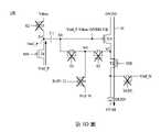
請參閱第5圖,第5圖描述根據本揭示的其他部分實施例所繪示的一畫素電路200。相較於第1圖的畫素電路100,第5圖的畫素電路200更包含一電晶體T7。如第5圖所示,電晶體T7的第一端耦接於氧化物電晶體TO的第一端,電晶體T7的第二端耦接於節點N3,且電晶體T7的控制端接收第一控制訊號S2。畫素電路200的其餘設置與操作與前述實施例類似,故不在此贅述。Please refer to FIG. 5 , which depicts a
請參閱第6圖,第6圖描述根據本揭示的其他部分實施例所繪示的一畫素電路200。相較於第1圖的畫素電路100,第6圖的畫素電路200更包含一電晶體T7。如第6圖所示,電晶體T7的第一端耦接於節點N1,電晶體T7的第二端耦接於氧化物電晶體TO的第二端,且電晶體T7的控制端接收第一控制訊號S2。畫素電路200的其餘設置與操作與前述實施例類似,故不在此贅述。Please refer to FIG. 6 . FIG. 6 depicts a
綜上,在維持前一幀畫面訊號的期間Fs中,本揭示不寫入新的資料電壓Vdata至畫素電路,但仍對發光元件OLED的陽極端進行重置,使得發光元件OLED不會有殘存的電荷影響發光亮度。藉由氧化物電晶體TO的設計,驅動電晶體TD的控制端的電壓準位較能保持與在進行畫面訊號更新的期間Fd中相近的電壓準位。如此一來,便能在降低畫面更新率時(即在低幀數模式下),達到節省功耗並穩定發光亮度,避免產生閃爍的現象。To sum up, during the period Fs of maintaining the previous frame signal, this disclosure does not write new data voltage Vdata to the pixel circuit, but still resets the anode terminal of the light-emitting element OLED, so that the light-emitting element OLED will not be damaged. The remaining charge affects the luminance of light emission. With the design of the oxide transistor TO, the voltage level of the control terminal of the driving transistor TD can be kept close to the voltage level during the period Fd of updating the picture signal. In this way, when the frame update rate is reduced (that is, in the low frame rate mode), power consumption can be saved and the brightness of the light can be stabilized to avoid flickering.
雖然本揭示內容已以實施方式揭露如上,然其並非用以限定本揭示內容,所屬技術領域具有通常知識者在不脫離本揭示內容之精神和範圍內,當可作各種更動與潤飾,因此本揭示內容之保護範圍當視後附之申請專利範圍所界定者為準。Although the present disclosure has been disclosed above in terms of implementation, it is not intended to limit the present disclosure. Those skilled in the art can make various changes and modifications without departing from the spirit and scope of the present disclosure. Therefore, this disclosure The scope of protection of the disclosed content shall be subject to the definition of the appended patent application scope.
100,200:畫素電路 T1,T2,T3,T4,T5,T6,T7:電晶體 TD:驅動電晶體 TO:氧化物電晶體 C1:電容 N1,N2,N3,N4:節點 OLED:發光元件 S1,S2,S3:控制訊號 EM:發光控制訊號 Vdata:資料電壓 OVDD:系統高電壓 OVSS:系統低電壓 Vref_N,Vref_P:參考電壓 Vth:臨界電壓 Id:驅動電流 Fd,Fs:期間 P1,P2,P3,P4:子期間100,200: pixel circuit T1, T2, T3, T4, T5, T6, T7: Transistor TD: drive transistor TO: oxide transistor C1: capacitance N1, N2, N3, N4: nodes OLED: light emitting element S1, S2, S3: control signal EM: Luminous control signal Vdata: data voltage OVDD: system high voltage OVSS: System Low Voltage Vref_N, Vref_P: reference voltage Vth: critical voltage Id: drive current Fd, Fs: period P1,P2,P3,P4: sub-period
第1圖係根據本揭示內容的部分實施例繪示一種畫素電路的示意圖。 第2圖係根據本揭示內容的部分實施例繪示一種畫素電路中的第一控制訊號、第二控制訊號、第三控制訊號與發光控制訊號的時序圖。 第3A~3D圖係根據本揭示內容的部分實施例繪示一種畫素電路運作於不同期間的示意圖。 第4圖係根據本揭示內容的其他部分實施例繪示一種畫素電路中的第一控制訊號、第二控制訊號、第三控制訊號與發光控制訊號的時序圖。 第5圖係根據本揭示內容的其他部分實施例繪示一種畫素電路的示意圖。 第6圖係根據本揭示內容的其他部分實施例繪示一種畫素電路的示意圖。FIG. 1 is a schematic diagram of a pixel circuit according to some embodiments of the disclosure. FIG. 2 is a timing diagram of a first control signal, a second control signal, a third control signal and a light-emitting control signal in a pixel circuit according to some embodiments of the present disclosure. FIGS. 3A-3D are schematic diagrams illustrating a pixel circuit operating in different periods according to some embodiments of the present disclosure. FIG. 4 is a timing diagram of a first control signal, a second control signal, a third control signal and a light-emitting control signal in a pixel circuit according to other embodiments of the present disclosure. FIG. 5 is a schematic diagram of a pixel circuit according to other embodiments of the disclosure. FIG. 6 is a schematic diagram of a pixel circuit according to other embodiments of the disclosure.
國內寄存資訊(請依寄存機構、日期、號碼順序註記) 無 國外寄存資訊(請依寄存國家、機構、日期、號碼順序註記) 無Domestic deposit information (please note in order of depositor, date, and number) none Overseas storage information (please note in order of storage country, institution, date, and number) none
100:畫素電路100:Pixel circuit
T1,T2,T3,T4,T5,T6:電晶體T1, T2, T3, T4, T5, T6: Transistor
TD:驅動電晶體TD: drive transistor
TO:氧化物電晶體TO: oxide transistor
C1:電容C1: capacitance
N1,N2,N3,N4:節點N1, N2, N3, N4: nodes
OLED:發光元件OLED: light emitting element
S1,S2,S3:控制訊號S1, S2, S3: control signal
EM:發光控制訊號EM: Luminous control signal
Vdata:資料電壓Vdata: data voltage
OVDD:系統高電壓OVDD: system high voltage
OVSS:系統低電壓OVSS: System Low Voltage
Vref_N,Vref_P:參考電壓Vref_N, Vref_P: reference voltage
Claims (10)
Translated fromChinesePriority Applications (2)
| Application Number | Priority Date | Filing Date | Title |
|---|---|---|---|
| TW110116982ATWI773313B (en) | 2021-05-11 | 2021-05-11 | Pixel circuit and driving method thereof |
| CN202111367139.6ACN113870794B (en) | 2021-05-11 | 2021-11-18 | Pixel circuit and driving method thereof |
Applications Claiming Priority (1)
| Application Number | Priority Date | Filing Date | Title |
|---|---|---|---|
| TW110116982ATWI773313B (en) | 2021-05-11 | 2021-05-11 | Pixel circuit and driving method thereof |
Publications (2)
| Publication Number | Publication Date |
|---|---|
| TWI773313B TWI773313B (en) | 2022-08-01 |
| TW202244873Atrue TW202244873A (en) | 2022-11-16 |
Family
ID=78984916
Family Applications (1)
| Application Number | Title | Priority Date | Filing Date |
|---|---|---|---|
| TW110116982ATWI773313B (en) | 2021-05-11 | 2021-05-11 | Pixel circuit and driving method thereof |
Country Status (2)
| Country | Link |
|---|---|
| CN (1) | CN113870794B (en) |
| TW (1) | TWI773313B (en) |
Cited By (1)
| Publication number | Priority date | Publication date | Assignee | Title |
|---|---|---|---|---|
| TWI889339B (en)* | 2024-05-14 | 2025-07-01 | 友達光電股份有限公司 | Pixel circuit and method for driving the same |
Families Citing this family (2)
| Publication number | Priority date | Publication date | Assignee | Title |
|---|---|---|---|---|
| CN115933237B (en)* | 2022-12-16 | 2024-07-09 | 业成科技(成都)有限公司 | Display device and method of operating the same |
| TWI889276B (en)* | 2024-04-08 | 2025-07-01 | 友達光電股份有限公司 | Pixel circuit and driving method thereof |
Family Cites Families (13)
| Publication number | Priority date | Publication date | Assignee | Title |
|---|---|---|---|---|
| CN102820006B (en)* | 2012-08-02 | 2015-10-14 | 京东方科技集团股份有限公司 | A kind of image element circuit of compensating threshold voltage drift and thin film transistor backplane |
| CN103187423B (en)* | 2013-02-04 | 2016-03-23 | 合肥京东方光电科技有限公司 | A kind of oxide film transistor array substrate and preparation method thereof, display floater |
| CN103715266A (en)* | 2013-12-25 | 2014-04-09 | 京东方科技集团股份有限公司 | Oxide thin-film transistor, manufacturing method of array substrate and display device |
| CN104064149B (en)* | 2014-07-07 | 2016-07-06 | 深圳市华星光电技术有限公司 | Image element circuit, the display floater possessing this image element circuit and display |
| CN106097964B (en)* | 2016-08-22 | 2018-09-18 | 京东方科技集团股份有限公司 | Pixel circuit, display panel, display equipment and driving method |
| CN106710528B (en)* | 2017-01-23 | 2019-03-12 | 上海天马有机发光显示技术有限公司 | Organic light emissive pixels driving circuit, driving method and organic light emitting display panel |
| KR102592012B1 (en)* | 2017-12-20 | 2023-10-24 | 삼성디스플레이 주식회사 | Pixel and organic light emittng display device including the pixel |
| CN109410836A (en)* | 2018-12-05 | 2019-03-01 | 武汉华星光电半导体显示技术有限公司 | OLED pixel driving circuit and display panel |
| KR102665185B1 (en)* | 2019-06-12 | 2024-05-16 | 삼성디스플레이 주식회사 | Display device |
| KR102681664B1 (en)* | 2019-06-12 | 2024-07-05 | 엘지디스플레이 주식회사 | Foldable display and driving method thereof |
| KR102710739B1 (en)* | 2019-10-25 | 2024-09-30 | 삼성디스플레이 주식회사 | Pixel and display device having the same |
| CN110752219B (en)* | 2019-10-29 | 2022-07-26 | 昆山国显光电有限公司 | A thin film transistor and display panel |
| CN110930949A (en)* | 2019-12-17 | 2020-03-27 | 昆山国显光电有限公司 | Pixel circuit and display panel |
- 2021
- 2021-05-11TWTW110116982Apatent/TWI773313B/enactive
- 2021-11-18CNCN202111367139.6Apatent/CN113870794B/enactiveActive
Cited By (1)
| Publication number | Priority date | Publication date | Assignee | Title |
|---|---|---|---|---|
| TWI889339B (en)* | 2024-05-14 | 2025-07-01 | 友達光電股份有限公司 | Pixel circuit and method for driving the same |
Also Published As
| Publication number | Publication date |
|---|---|
| CN113870794B (en) | 2023-09-26 |
| CN113870794A (en) | 2021-12-31 |
| TWI773313B (en) | 2022-08-01 |
Similar Documents
| Publication | Publication Date | Title |
|---|---|---|
| CN116597777B (en) | Display panel and display device | |
| CN110660360B (en) | Pixel circuit and driving method thereof, and display panel | |
| US20240119897A1 (en) | Pixel Circuit and Driving Method Therefor and Display Panel | |
| WO2020052287A1 (en) | Pixel circuit and driving method therefor, and display device | |
| CN113950715A (en) | Pixel circuit, driving method thereof and display device | |
| JP6847042B2 (en) | Display device equipped with light emission control circuit and light emission control circuit and its driving method | |
| CN114582287B (en) | Display panel and display device | |
| WO2020233491A1 (en) | Pixel circuit and drive method therefor, array substrate, and display device | |
| TWI720655B (en) | Pixel circuit and driving method thereof | |
| CN111754939B (en) | Pixel circuit, driving method thereof and display device | |
| CN112102778A (en) | Pixel circuit, driving method thereof, display substrate and display device | |
| CN113870794B (en) | Pixel circuit and driving method thereof | |
| WO2020186933A1 (en) | Pixel circuit, method for driving same, electroluminescent display panel, and display device | |
| JP7114255B2 (en) | Pixel driving circuit and its driving method, array substrate, display device | |
| JP2022534548A (en) | Pixel compensation circuit, display panel, driving method, and display device | |
| CN109559686A (en) | Pixel circuit, driving method, electroluminescence display panel and display device | |
| WO2021035414A1 (en) | Pixel circuit and driving method therefor, and display substrate and driving method therefor, and display device | |
| CN113658554B (en) | Pixel driving circuit, pixel driving method and display device | |
| CN113066439B (en) | A pixel circuit, a driving method, an electroluminescent display panel, and a display device | |
| CN108538247A (en) | Pixel circuit and its driving method, display panel and display equipment | |
| CN109256086A (en) | Pixel circuit and its driving method, array substrate, display panel | |
| CN111968581A (en) | Driving method of pixel circuit | |
| CN112530341B (en) | Pixel circuit | |
| CN117296092A (en) | Pixel circuit, driving method thereof, display panel and display device | |
| CN114550655A (en) | display device |