TW202243236A - Semiconductor structure - Google Patents
Semiconductor structureDownload PDFInfo
- Publication number
- TW202243236A TW202243236ATW111103567ATW111103567ATW202243236ATW 202243236 ATW202243236 ATW 202243236ATW 111103567 ATW111103567 ATW 111103567ATW 111103567 ATW111103567 ATW 111103567ATW 202243236 ATW202243236 ATW 202243236A
- Authority
- TW
- Taiwan
- Prior art keywords
- feature
- source
- layer
- backside
- drain
- Prior art date
Links
- 239000004065semiconductorSubstances0.000titleclaimsabstractdescription42
- 238000003860storageMethods0.000claimsabstractdescription47
- 238000000034methodMethods0.000abstractdescription63
- 239000010410layerSubstances0.000description165
- 229910052751metalInorganic materials0.000description113
- 239000002184metalSubstances0.000description113
- 230000008569processEffects0.000description28
- 239000000758substrateSubstances0.000description27
- 239000000463materialSubstances0.000description22
- 239000002086nanomaterialSubstances0.000description21
- PXHVJJICTQNCMI-UHFFFAOYSA-NNickelChemical compound[Ni]PXHVJJICTQNCMI-UHFFFAOYSA-N0.000description20
- 239000010949copperSubstances0.000description20
- 230000004888barrier functionEffects0.000description17
- 238000004519manufacturing processMethods0.000description17
- 229910021332silicideInorganic materials0.000description17
- FVBUAEGBCNSCDD-UHFFFAOYSA-Nsilicide(4-)Chemical compound[Si-4]FVBUAEGBCNSCDD-UHFFFAOYSA-N0.000description17
- XUIMIQQOPSSXEZ-UHFFFAOYSA-NSiliconChemical compound[Si]XUIMIQQOPSSXEZ-UHFFFAOYSA-N0.000description16
- 229910052710siliconInorganic materials0.000description16
- 239000010703siliconSubstances0.000description16
- 229910052581Si3N4Inorganic materials0.000description14
- VYPSYNLAJGMNEJ-UHFFFAOYSA-NSilicium dioxideChemical compoundO=[Si]=OVYPSYNLAJGMNEJ-UHFFFAOYSA-N0.000description12
- BASFCYQUMIYNBI-UHFFFAOYSA-NplatinumChemical compound[Pt]BASFCYQUMIYNBI-UHFFFAOYSA-N0.000description12
- 239000010936titaniumSubstances0.000description12
- 229910052721tungstenInorganic materials0.000description12
- 239000010937tungstenSubstances0.000description12
- HQVNEWCFYHHQES-UHFFFAOYSA-Nsilicon nitrideChemical compoundN12[Si]34N5[Si]62N3[Si]51N64HQVNEWCFYHHQES-UHFFFAOYSA-N0.000description11
- RYGMFSIKBFXOCR-UHFFFAOYSA-NCopperChemical compound[Cu]RYGMFSIKBFXOCR-UHFFFAOYSA-N0.000description10
- KJTLSVCANCCWHF-UHFFFAOYSA-NRutheniumChemical compound[Ru]KJTLSVCANCCWHF-UHFFFAOYSA-N0.000description10
- MCMNRKCIXSYSNV-UHFFFAOYSA-NZirconium dioxideChemical compoundO=[Zr]=OMCMNRKCIXSYSNV-UHFFFAOYSA-N0.000description10
- 229910017052cobaltInorganic materials0.000description10
- 239000010941cobaltSubstances0.000description10
- 229910052802copperInorganic materials0.000description10
- 230000036961partial effectEffects0.000description10
- 229910052707rutheniumInorganic materials0.000description10
- WFKWXMTUELFFGS-UHFFFAOYSA-NtungstenChemical compound[W]WFKWXMTUELFFGS-UHFFFAOYSA-N0.000description10
- 229910000577Silicon-germaniumInorganic materials0.000description9
- 125000006850spacer groupChemical group0.000description9
- NRTOMJZYCJJWKI-UHFFFAOYSA-NTitanium nitrideChemical compound[Ti]#NNRTOMJZYCJJWKI-UHFFFAOYSA-N0.000description8
- 229910052782aluminiumInorganic materials0.000description8
- XAGFODPZIPBFFR-UHFFFAOYSA-NaluminiumChemical compound[Al]XAGFODPZIPBFFR-UHFFFAOYSA-N0.000description8
- GUTLYIVDDKVIGB-UHFFFAOYSA-Ncobalt atomChemical compound[Co]GUTLYIVDDKVIGB-UHFFFAOYSA-N0.000description8
- 229910052759nickelInorganic materials0.000description8
- 229910052715tantalumInorganic materials0.000description8
- GUVRBAGPIYLISA-UHFFFAOYSA-Ntantalum atomChemical compound[Ta]GUVRBAGPIYLISA-UHFFFAOYSA-N0.000description8
- MZLGASXMSKOWSE-UHFFFAOYSA-Ntantalum nitrideChemical compound[Ta]#NMZLGASXMSKOWSE-UHFFFAOYSA-N0.000description8
- -1aluminum silicon oxideChemical compound0.000description7
- 238000005229chemical vapour depositionMethods0.000description7
- 239000000203mixtureSubstances0.000description7
- RTAQQCXQSZGOHL-UHFFFAOYSA-NTitaniumChemical compound[Ti]RTAQQCXQSZGOHL-UHFFFAOYSA-N0.000description6
- 238000002955isolationMethods0.000description6
- 229910052719titaniumInorganic materials0.000description6
- 238000000231atomic layer depositionMethods0.000description5
- 239000012212insulatorSubstances0.000description5
- ZOXJGFHDIHLPTG-UHFFFAOYSA-NBoronChemical compound[B]ZOXJGFHDIHLPTG-UHFFFAOYSA-N0.000description4
- LEVVHYCKPQWKOP-UHFFFAOYSA-N[Si].[Ge]Chemical compound[Si].[Ge]LEVVHYCKPQWKOP-UHFFFAOYSA-N0.000description4
- UGACIEPFGXRWCH-UHFFFAOYSA-N[Si].[Ti]Chemical compound[Si].[Ti]UGACIEPFGXRWCH-UHFFFAOYSA-N0.000description4
- 230000008901benefitEffects0.000description4
- 229910052796boronInorganic materials0.000description4
- 239000005380borophosphosilicate glassSubstances0.000description4
- 238000000151depositionMethods0.000description4
- 239000005360phosphosilicate glassSubstances0.000description4
- 229910052697platinumInorganic materials0.000description4
- HBMJWWWQQXIZIP-UHFFFAOYSA-Nsilicon carbideChemical compound[Si+]#[C-]HBMJWWWQQXIZIP-UHFFFAOYSA-N0.000description4
- 229910052814silicon oxideInorganic materials0.000description4
- BOTDANWDWHJENH-UHFFFAOYSA-NTetraethyl orthosilicateChemical compoundCCO[Si](OCC)(OCC)OCCBOTDANWDWHJENH-UHFFFAOYSA-N0.000description3
- RVSGESPTHDDNTH-UHFFFAOYSA-Nalumane;tantalumChemical compound[AlH3].[Ta]RVSGESPTHDDNTH-UHFFFAOYSA-N0.000description3
- 239000003989dielectric materialSubstances0.000description3
- XEEYBQQBJWHFJM-UHFFFAOYSA-NironSubstances[Fe]XEEYBQQBJWHFJM-UHFFFAOYSA-N0.000description3
- TWNQGVIAIRXVLR-UHFFFAOYSA-Noxo(oxoalumanyloxy)alumaneChemical compoundO=[Al]O[Al]=OTWNQGVIAIRXVLR-UHFFFAOYSA-N0.000description3
- 238000005240physical vapour depositionMethods0.000description3
- 229910010271silicon carbideInorganic materials0.000description3
- 239000000377silicon dioxideSubstances0.000description3
- 235000012239silicon dioxideNutrition0.000description3
- 230000005641tunnelingEffects0.000description3
- 229910018072Al 2 O 3Inorganic materials0.000description2
- ZOKXTWBITQBERF-UHFFFAOYSA-NMolybdenumChemical compound[Mo]ZOKXTWBITQBERF-UHFFFAOYSA-N0.000description2
- 229910045601alloyInorganic materials0.000description2
- 239000000956alloySubstances0.000description2
- UQZIWOQVLUASCR-UHFFFAOYSA-Nalumane;titaniumChemical compound[AlH3].[Ti]UQZIWOQVLUASCR-UHFFFAOYSA-N0.000description2
- 238000010586diagramMethods0.000description2
- 239000002019doping agentSubstances0.000description2
- 238000007772electroless platingMethods0.000description2
- 238000005516engineering processMethods0.000description2
- 238000005530etchingMethods0.000description2
- 230000005669field effectEffects0.000description2
- 230000006870functionEffects0.000description2
- 239000005350fused silica glassSubstances0.000description2
- 229910052732germaniumInorganic materials0.000description2
- GNPVGFCGXDBREM-UHFFFAOYSA-Ngermanium atomChemical compound[Ge]GNPVGFCGXDBREM-UHFFFAOYSA-N0.000description2
- 230000010354integrationEffects0.000description2
- 239000011229interlayerSubstances0.000description2
- SHMWNGFNWYELHA-UHFFFAOYSA-Niridium manganeseChemical compound[Mn].[Ir]SHMWNGFNWYELHA-UHFFFAOYSA-N0.000description2
- 229910052742ironInorganic materials0.000description2
- 239000000395magnesium oxideSubstances0.000description2
- CPLXHLVBOLITMK-UHFFFAOYSA-Nmagnesium oxideInorganic materials[Mg]=OCPLXHLVBOLITMK-UHFFFAOYSA-N0.000description2
- AXZKOIWUVFPNLO-UHFFFAOYSA-Nmagnesium;oxygen(2-)Chemical compound[O-2].[Mg+2]AXZKOIWUVFPNLO-UHFFFAOYSA-N0.000description2
- NFFIWVVINABMKP-UHFFFAOYSA-NmethylidynetantalumChemical compound[Ta]#CNFFIWVVINABMKP-UHFFFAOYSA-N0.000description2
- 229910052750molybdenumInorganic materials0.000description2
- 239000011733molybdenumSubstances0.000description2
- 239000002135nanosheetSubstances0.000description2
- 239000002070nanowireSubstances0.000description2
- PEUPIGGLJVUNEU-UHFFFAOYSA-Nnickel siliconChemical compound[Si].[Ni]PEUPIGGLJVUNEU-UHFFFAOYSA-N0.000description2
- RVTZCBVAJQQJTK-UHFFFAOYSA-Noxygen(2-);zirconium(4+)Chemical compound[O-2].[O-2].[Zr+4]RVTZCBVAJQQJTK-UHFFFAOYSA-N0.000description2
- 238000000623plasma-assisted chemical vapour depositionMethods0.000description2
- 239000011241protective layerSubstances0.000description2
- 239000003870refractory metalSubstances0.000description2
- 239000010948rhodiumSubstances0.000description2
- WNUPENMBHHEARK-UHFFFAOYSA-Nsilicon tungstenChemical compound[Si].[W]WNUPENMBHHEARK-UHFFFAOYSA-N0.000description2
- 229910003468tantalcarbideInorganic materials0.000description2
- 229910001928zirconium oxideInorganic materials0.000description2
- 229910019311(Ba,Sr)TiOInorganic materials0.000description1
- 229910000980Aluminium gallium arsenideInorganic materials0.000description1
- PIGFYZPCRLYGLF-UHFFFAOYSA-NAluminum nitrideChemical compound[Al]#NPIGFYZPCRLYGLF-UHFFFAOYSA-N0.000description1
- JBRZTFJDHDCESZ-UHFFFAOYSA-NAsGaChemical compound[As]#[Ga]JBRZTFJDHDCESZ-UHFFFAOYSA-N0.000description1
- 229910003321CoFeInorganic materials0.000description1
- 229910019236CoFeBInorganic materials0.000description1
- 229910018979CoPtInorganic materials0.000description1
- 206010010144Completed suicideDiseases0.000description1
- 229910015136FeMnInorganic materials0.000description1
- 229910005540GaPInorganic materials0.000description1
- 229910001218Gallium arsenideInorganic materials0.000description1
- 229910000530Gallium indium arsenideInorganic materials0.000description1
- 229910004129HfSiOInorganic materials0.000description1
- 229910000673Indium arsenideInorganic materials0.000description1
- GPXJNWSHGFTCBW-UHFFFAOYSA-NIndium phosphideChemical compound[In]#PGPXJNWSHGFTCBW-UHFFFAOYSA-N0.000description1
- 229910001030Iron–nickel alloyInorganic materials0.000description1
- OAICVXFJPJFONN-UHFFFAOYSA-NPhosphorusChemical compound[P]OAICVXFJPJFONN-UHFFFAOYSA-N0.000description1
- 229910002367SrTiOInorganic materials0.000description1
- 229910004491TaAlNInorganic materials0.000description1
- GWEVSGVZZGPLCZ-UHFFFAOYSA-NTitan oxideChemical compoundO=[Ti]=OGWEVSGVZZGPLCZ-UHFFFAOYSA-N0.000description1
- 229910006501ZrSiOInorganic materials0.000description1
- ZDZZPLGHBXACDA-UHFFFAOYSA-N[B].[Fe].[Co]Chemical compound[B].[Fe].[Co]ZDZZPLGHBXACDA-UHFFFAOYSA-N0.000description1
- HMDDXIMCDZRSNE-UHFFFAOYSA-N[C].[Si]Chemical compound[C].[Si]HMDDXIMCDZRSNE-UHFFFAOYSA-N0.000description1
- OBZUDFAHIZFVHI-UHFFFAOYSA-N[La].[Si]=OChemical compound[La].[Si]=OOBZUDFAHIZFVHI-UHFFFAOYSA-N0.000description1
- DBOSVWZVMLOAEU-UHFFFAOYSA-N[O-2].[Hf+4].[La+3]Chemical compound[O-2].[Hf+4].[La+3]DBOSVWZVMLOAEU-UHFFFAOYSA-N0.000description1
- ILCYGSITMBHYNK-UHFFFAOYSA-N[Si]=O.[Hf]Chemical compound[Si]=O.[Hf]ILCYGSITMBHYNK-UHFFFAOYSA-N0.000description1
- 230000003466anti-cipated effectEffects0.000description1
- 229910052785arsenicInorganic materials0.000description1
- RQNWIZPPADIBDY-UHFFFAOYSA-Narsenic atomChemical compound[As]RQNWIZPPADIBDY-UHFFFAOYSA-N0.000description1
- QVGXLLKOCUKJST-UHFFFAOYSA-Natomic oxygenChemical compound[O]QVGXLLKOCUKJST-UHFFFAOYSA-N0.000description1
- 230000015572biosynthetic processEffects0.000description1
- 230000000903blocking effectEffects0.000description1
- 239000011248coating agentSubstances0.000description1
- 238000000576coating methodMethods0.000description1
- 150000001875compoundsChemical class0.000description1
- PMHQVHHXPFUNSP-UHFFFAOYSA-Mcopper(1+);methylsulfanylmethane;bromideChemical compoundBr[Cu].CSCPMHQVHHXPFUNSP-UHFFFAOYSA-M0.000description1
- 238000013500data storageMethods0.000description1
- 230000007423decreaseEffects0.000description1
- 230000003247decreasing effectEffects0.000description1
- 230000008021depositionEffects0.000description1
- OKZIUSOJQLYFSE-UHFFFAOYSA-NdifluoroboronChemical compoundF[B]FOKZIUSOJQLYFSE-UHFFFAOYSA-N0.000description1
- 238000001312dry etchingMethods0.000description1
- 239000000945fillerSubstances0.000description1
- HZXMRANICFIONG-UHFFFAOYSA-Ngallium phosphideChemical compound[Ga]#PHZXMRANICFIONG-UHFFFAOYSA-N0.000description1
- 239000011521glassSubstances0.000description1
- 239000003292glueSubstances0.000description1
- ZQXQADNTSSMHJI-UHFFFAOYSA-Nhafnium(4+) oxygen(2-) tantalum(5+)Chemical compound[O-2].[Ta+5].[Hf+4]ZQXQADNTSSMHJI-UHFFFAOYSA-N0.000description1
- KQHQLIAOAVMAOW-UHFFFAOYSA-Nhafnium(4+) oxygen(2-) zirconium(4+)Chemical compound[O--].[O--].[O--].[O--].[Zr+4].[Hf+4]KQHQLIAOAVMAOW-UHFFFAOYSA-N0.000description1
- KUVFGOLWQIXGBP-UHFFFAOYSA-Nhafnium(4+);oxygen(2-);titanium(4+)Chemical compound[O-2].[O-2].[O-2].[O-2].[Ti+4].[Hf+4]KUVFGOLWQIXGBP-UHFFFAOYSA-N0.000description1
- CJNBYAVZURUTKZ-UHFFFAOYSA-Nhafnium(iv) oxideChemical compoundO=[Hf]=OCJNBYAVZURUTKZ-UHFFFAOYSA-N0.000description1
- 238000002513implantationMethods0.000description1
- WPYVAWXEWQSOGY-UHFFFAOYSA-Nindium antimonideChemical compound[Sb]#[In]WPYVAWXEWQSOGY-UHFFFAOYSA-N0.000description1
- RPQDHPTXJYYUPQ-UHFFFAOYSA-Nindium arsenideChemical compound[In]#[As]RPQDHPTXJYYUPQ-UHFFFAOYSA-N0.000description1
- 229910052741iridiumInorganic materials0.000description1
- GKOZUEZYRPOHIO-UHFFFAOYSA-Niridium atomChemical compound[Ir]GKOZUEZYRPOHIO-UHFFFAOYSA-N0.000description1
- DALUDRGQOYMVLD-UHFFFAOYSA-Niron manganeseChemical compound[Mn].[Fe]DALUDRGQOYMVLD-UHFFFAOYSA-N0.000description1
- MRELNEQAGSRDBK-UHFFFAOYSA-Nlanthanum(3+);oxygen(2-)Chemical compound[O-2].[O-2].[O-2].[La+3].[La+3]MRELNEQAGSRDBK-UHFFFAOYSA-N0.000description1
- IGOJMROYPFZEOR-UHFFFAOYSA-Nmanganese platinumChemical compound[Mn].[Pt]IGOJMROYPFZEOR-UHFFFAOYSA-N0.000description1
- GBZQODYDRJQFHG-UHFFFAOYSA-Nmanganese rhodiumChemical compound[Mn].[Rh]GBZQODYDRJQFHG-UHFFFAOYSA-N0.000description1
- 239000007769metal materialSubstances0.000description1
- 238000013508migrationMethods0.000description1
- 150000004767nitridesChemical class0.000description1
- SIWVEOZUMHYXCS-UHFFFAOYSA-Noxo(oxoyttriooxy)yttriumChemical compoundO=[Y]O[Y]=OSIWVEOZUMHYXCS-UHFFFAOYSA-N0.000description1
- 229910052760oxygenInorganic materials0.000description1
- 239000001301oxygenSubstances0.000description1
- BPUBBGLMJRNUCC-UHFFFAOYSA-Noxygen(2-);tantalum(5+)Chemical compound[O-2].[O-2].[O-2].[O-2].[O-2].[Ta+5].[Ta+5]BPUBBGLMJRNUCC-UHFFFAOYSA-N0.000description1
- 230000002093peripheral effectEffects0.000description1
- 229910052698phosphorusInorganic materials0.000description1
- 239000011574phosphorusSubstances0.000description1
- 239000002861polymer materialSubstances0.000description1
- 230000009467reductionEffects0.000description1
- 230000002829reductive effectEffects0.000description1
- 229910052703rhodiumInorganic materials0.000description1
- MHOVAHRLVXNVSD-UHFFFAOYSA-Nrhodium atomChemical compound[Rh]MHOVAHRLVXNVSD-UHFFFAOYSA-N0.000description1
- 239000010980sapphireSubstances0.000description1
- 229910052594sapphireInorganic materials0.000description1
- 238000000926separation methodMethods0.000description1
- 239000005368silicate glassSubstances0.000description1
- HWEYZGSCHQNNEH-UHFFFAOYSA-Nsilicon tantalumChemical compound[Si].[Ta]HWEYZGSCHQNNEH-UHFFFAOYSA-N0.000description1
- 230000003068static effectEffects0.000description1
- 238000006467substitution reactionMethods0.000description1
- 238000001039wet etchingMethods0.000description1
Images


Classifications
- H—ELECTRICITY
- H10—SEMICONDUCTOR DEVICES; ELECTRIC SOLID-STATE DEVICES NOT OTHERWISE PROVIDED FOR
- H10D—INORGANIC ELECTRIC SEMICONDUCTOR DEVICES
- H10D30/00—Field-effect transistors [FET]
- H10D30/40—FETs having zero-dimensional [0D], one-dimensional [1D] or two-dimensional [2D] charge carrier gas channels
- H10D30/43—FETs having zero-dimensional [0D], one-dimensional [1D] or two-dimensional [2D] charge carrier gas channels having 1D charge carrier gas channels, e.g. quantum wire FETs or transistors having 1D quantum-confined channels
- H—ELECTRICITY
- H01—ELECTRIC ELEMENTS
- H01L—SEMICONDUCTOR DEVICES NOT COVERED BY CLASS H10
- H01L21/00—Processes or apparatus adapted for the manufacture or treatment of semiconductor or solid state devices or of parts thereof
- H01L21/70—Manufacture or treatment of devices consisting of a plurality of solid state components formed in or on a common substrate or of parts thereof; Manufacture of integrated circuit devices or of parts thereof
- H01L21/71—Manufacture of specific parts of devices defined in group H01L21/70
- H01L21/768—Applying interconnections to be used for carrying current between separate components within a device comprising conductors and dielectrics
- H01L21/76897—Formation of self-aligned vias or contact plugs, i.e. involving a lithographically uncritical step
- H—ELECTRICITY
- H01—ELECTRIC ELEMENTS
- H01L—SEMICONDUCTOR DEVICES NOT COVERED BY CLASS H10
- H01L23/00—Details of semiconductor or other solid state devices
- H01L23/52—Arrangements for conducting electric current within the device in operation from one component to another, i.e. interconnections, e.g. wires, lead frames
- H01L23/522—Arrangements for conducting electric current within the device in operation from one component to another, i.e. interconnections, e.g. wires, lead frames including external interconnections consisting of a multilayer structure of conductive and insulating layers inseparably formed on the semiconductor body
- H01L23/528—Layout of the interconnection structure
- H01L23/5286—Arrangements of power or ground buses
- H—ELECTRICITY
- H10—SEMICONDUCTOR DEVICES; ELECTRIC SOLID-STATE DEVICES NOT OTHERWISE PROVIDED FOR
- H10B—ELECTRONIC MEMORY DEVICES
- H10B61/00—Magnetic memory devices, e.g. magnetoresistive RAM [MRAM] devices
- H10B61/20—Magnetic memory devices, e.g. magnetoresistive RAM [MRAM] devices comprising components having three or more electrodes, e.g. transistors
- H10B61/22—Magnetic memory devices, e.g. magnetoresistive RAM [MRAM] devices comprising components having three or more electrodes, e.g. transistors of the field-effect transistor [FET] type
- H—ELECTRICITY
- H10—SEMICONDUCTOR DEVICES; ELECTRIC SOLID-STATE DEVICES NOT OTHERWISE PROVIDED FOR
- H10D—INORGANIC ELECTRIC SEMICONDUCTOR DEVICES
- H10D30/00—Field-effect transistors [FET]
- H10D30/01—Manufacture or treatment
- H10D30/014—Manufacture or treatment of FETs having zero-dimensional [0D] or one-dimensional [1D] channels, e.g. quantum wire FETs, single-electron transistors [SET] or Coulomb blockade transistors
- H—ELECTRICITY
- H10—SEMICONDUCTOR DEVICES; ELECTRIC SOLID-STATE DEVICES NOT OTHERWISE PROVIDED FOR
- H10D—INORGANIC ELECTRIC SEMICONDUCTOR DEVICES
- H10D30/00—Field-effect transistors [FET]
- H10D30/01—Manufacture or treatment
- H10D30/021—Manufacture or treatment of FETs having insulated gates [IGFET]
- H10D30/031—Manufacture or treatment of FETs having insulated gates [IGFET] of thin-film transistors [TFT]
- H—ELECTRICITY
- H10—SEMICONDUCTOR DEVICES; ELECTRIC SOLID-STATE DEVICES NOT OTHERWISE PROVIDED FOR
- H10D—INORGANIC ELECTRIC SEMICONDUCTOR DEVICES
- H10D30/00—Field-effect transistors [FET]
- H10D30/60—Insulated-gate field-effect transistors [IGFET]
- H10D30/67—Thin-film transistors [TFT]
- H10D30/6704—Thin-film transistors [TFT] having supplementary regions or layers in the thin films or in the insulated bulk substrates for controlling properties of the device
- H10D30/6713—Thin-film transistors [TFT] having supplementary regions or layers in the thin films or in the insulated bulk substrates for controlling properties of the device characterised by the properties of the source or drain regions, e.g. compositions or sectional shapes
- H—ELECTRICITY
- H10—SEMICONDUCTOR DEVICES; ELECTRIC SOLID-STATE DEVICES NOT OTHERWISE PROVIDED FOR
- H10D—INORGANIC ELECTRIC SEMICONDUCTOR DEVICES
- H10D30/00—Field-effect transistors [FET]
- H10D30/60—Insulated-gate field-effect transistors [IGFET]
- H10D30/67—Thin-film transistors [TFT]
- H10D30/6729—Thin-film transistors [TFT] characterised by the electrodes
- H10D30/673—Thin-film transistors [TFT] characterised by the electrodes characterised by the shapes, relative sizes or dispositions of the gate electrodes
- H10D30/6735—Thin-film transistors [TFT] characterised by the electrodes characterised by the shapes, relative sizes or dispositions of the gate electrodes having gates fully surrounding the channels, e.g. gate-all-around
- H—ELECTRICITY
- H10—SEMICONDUCTOR DEVICES; ELECTRIC SOLID-STATE DEVICES NOT OTHERWISE PROVIDED FOR
- H10D—INORGANIC ELECTRIC SEMICONDUCTOR DEVICES
- H10D30/00—Field-effect transistors [FET]
- H10D30/60—Insulated-gate field-effect transistors [IGFET]
- H10D30/67—Thin-film transistors [TFT]
- H10D30/6757—Thin-film transistors [TFT] characterised by the structure of the channel, e.g. transverse or longitudinal shape or doping profile
- H—ELECTRICITY
- H10—SEMICONDUCTOR DEVICES; ELECTRIC SOLID-STATE DEVICES NOT OTHERWISE PROVIDED FOR
- H10D—INORGANIC ELECTRIC SEMICONDUCTOR DEVICES
- H10D62/00—Semiconductor bodies, or regions thereof, of devices having potential barriers
- H10D62/10—Shapes, relative sizes or dispositions of the regions of the semiconductor bodies; Shapes of the semiconductor bodies
- H10D62/117—Shapes of semiconductor bodies
- H10D62/118—Nanostructure semiconductor bodies
- H10D62/119—Nanowire, nanosheet or nanotube semiconductor bodies
- H10D62/121—Nanowire, nanosheet or nanotube semiconductor bodies oriented parallel to substrates
- H—ELECTRICITY
- H10—SEMICONDUCTOR DEVICES; ELECTRIC SOLID-STATE DEVICES NOT OTHERWISE PROVIDED FOR
- H10N—ELECTRIC SOLID-STATE DEVICES NOT OTHERWISE PROVIDED FOR
- H10N50/00—Galvanomagnetic devices
- H10N50/01—Manufacture or treatment
- H—ELECTRICITY
- H10—SEMICONDUCTOR DEVICES; ELECTRIC SOLID-STATE DEVICES NOT OTHERWISE PROVIDED FOR
- H10N—ELECTRIC SOLID-STATE DEVICES NOT OTHERWISE PROVIDED FOR
- H10N50/00—Galvanomagnetic devices
- H10N50/80—Constructional details
- H—ELECTRICITY
- H10—SEMICONDUCTOR DEVICES; ELECTRIC SOLID-STATE DEVICES NOT OTHERWISE PROVIDED FOR
- H10N—ELECTRIC SOLID-STATE DEVICES NOT OTHERWISE PROVIDED FOR
- H10N50/00—Galvanomagnetic devices
- H10N50/80—Constructional details
- H10N50/85—Materials of the active region
- B—PERFORMING OPERATIONS; TRANSPORTING
- B82—NANOTECHNOLOGY
- B82Y—SPECIFIC USES OR APPLICATIONS OF NANOSTRUCTURES; MEASUREMENT OR ANALYSIS OF NANOSTRUCTURES; MANUFACTURE OR TREATMENT OF NANOSTRUCTURES
- B82Y10/00—Nanotechnology for information processing, storage or transmission, e.g. quantum computing or single electron logic
- H—ELECTRICITY
- H01—ELECTRIC ELEMENTS
- H01L—SEMICONDUCTOR DEVICES NOT COVERED BY CLASS H10
- H01L21/00—Processes or apparatus adapted for the manufacture or treatment of semiconductor or solid state devices or of parts thereof
- H01L21/02—Manufacture or treatment of semiconductor devices or of parts thereof
- H01L21/04—Manufacture or treatment of semiconductor devices or of parts thereof the devices having potential barriers, e.g. a PN junction, depletion layer or carrier concentration layer
- H01L21/18—Manufacture or treatment of semiconductor devices or of parts thereof the devices having potential barriers, e.g. a PN junction, depletion layer or carrier concentration layer the devices having semiconductor bodies comprising elements of Group IV of the Periodic Table or AIIIBV compounds with or without impurities, e.g. doping materials
- H01L21/28—Manufacture of electrodes on semiconductor bodies using processes or apparatus not provided for in groups H01L21/20 - H01L21/268
- H01L21/283—Deposition of conductive or insulating materials for electrodes conducting electric current
- H01L21/285—Deposition of conductive or insulating materials for electrodes conducting electric current from a gas or vapour, e.g. condensation
- H01L21/28506—Deposition of conductive or insulating materials for electrodes conducting electric current from a gas or vapour, e.g. condensation of conductive layers
- H01L21/28512—Deposition of conductive or insulating materials for electrodes conducting electric current from a gas or vapour, e.g. condensation of conductive layers on semiconductor bodies comprising elements of Group IV of the Periodic Table
- H01L21/28518—Deposition of conductive or insulating materials for electrodes conducting electric current from a gas or vapour, e.g. condensation of conductive layers on semiconductor bodies comprising elements of Group IV of the Periodic Table the conductive layers comprising silicides
Landscapes
- Engineering & Computer Science (AREA)
- Physics & Mathematics (AREA)
- Power Engineering (AREA)
- General Physics & Mathematics (AREA)
- Computer Hardware Design (AREA)
- Microelectronics & Electronic Packaging (AREA)
- Condensed Matter Physics & Semiconductors (AREA)
- Manufacturing & Machinery (AREA)
- Geometry (AREA)
- Semiconductor Memories (AREA)
- Chemical & Material Sciences (AREA)
- Crystallography & Structural Chemistry (AREA)
- Nanotechnology (AREA)
- Non-Volatile Memory (AREA)
Abstract
Description
Translated fromChinese本揭露係有關於一種半導體結構及其形成方法,特別係有關於一種具有設置於後側互連結構中之儲存元件的半導體結構及其形成方法。The present disclosure relates to a semiconductor structure and a method for forming the same, and more particularly to a semiconductor structure with a storage device disposed in a backside interconnection structure and a method for forming the same.
半導體積體電路(integrated circuit, IC)工業已經歷了指數性的成長。技術在IC材料以及設計上的進步已經產生了好幾世代的IC,其中每一世代相較於先前世代都具有更小且更複雜的電路。在IC的進化過程中,功能密度(即:每單位晶片面積之互連裝置的數量)通常會增加,同時幾何尺寸(即:使用製造製程所能創建之最小組件(或線段))則會降低。這種微縮(scaling down)通常藉由增加生產效率以及減少相關成本的方式來提供益處。此種微縮亦增加了處理以及製造IC的複雜性。The semiconductor integrated circuit (IC) industry has experienced exponential growth. Advances in technology in IC materials and design have produced several generations of ICs, with each generation having smaller and more complex circuits than the previous generation. During the evolution of ICs, functional density (i.e., the number of interconnected devices per unit of die area) typically increases while geometry size (i.e., the smallest component (or line segment) that can be created using a manufacturing process) decreases . This scaling down typically provides benefits by increasing production efficiency and reducing associated costs. Such scaling also increases the complexity of handling and manufacturing the IC.
現今的電子裝置包含揮發性(volatile)或非揮發性(non-volatile)電子記憶體以儲存資料。揮發性記憶體在被供給電力時會儲存資料,而非揮發性記憶體則能夠在電源被移除時保持資料的儲存。對於下一世代的非揮發性記憶體技術,磁阻式隨機存取記憶體(magneto-resistive random-access memory, MRAM)是備受期待的候選者。MRAM裝置可被整合到設置於裝置基板上方的前側(frontside)互連結構之中。儘管現行的MRAM整合方案通常已足以滿足其預期目的,但是它們並非在所有方面都是完全令人滿意的。Today's electronic devices contain volatile or non-volatile electronic memory to store data. Volatile memory stores data when power is supplied, while non-volatile memory maintains data storage when power is removed. Magneto-resistive random-access memory (MRAM) is a highly anticipated candidate for the next generation of non-volatile memory technology. MRAM devices can be integrated into a frontside interconnect structure disposed above a device substrate. Although current MRAM integration schemes are generally adequate for their intended purposes, they are not entirely satisfactory in all respects.
本揭露實施例提供一種半導體結構。上述半導體結構包括源極特徵以及汲極特徵、源極特徵與汲極特徵之間的主動區、主動區上方的閘極結構、設置於源極特徵以及汲極特徵還有閘極結構上方的前側互連結構、設置於源極特徵以及汲極特徵還有閘極結構下方的後側互連結構、以及設置於後側互連結構之中的儲存元件。Embodiments of the disclosure provide a semiconductor structure. The semiconductor structure includes a source feature and a drain feature, an active region between the source feature and the drain feature, a gate structure above the active region, a front side disposed above the source feature, the drain feature and the gate structure The interconnection structure, the backside interconnection structure disposed under the source feature, the drain feature and the gate structure, and the storage element disposed in the backside interconnection structure.
本揭露實施例提供一種半導體結構。上述半導體結構包括第一源極特徵以及第二源極特徵、設置於第一源極特徵與第二源極特徵之間的汲極特徵、在第一源極特徵與汲極特徵之間延伸的第一主動區、在汲極特徵與第二源極特徵之間延伸的第二主動區、位於第一主動區上方的第一閘極結構、位於第二主動區上方的第二閘極結構、設置於第一源極特徵與第二源極特徵和第一閘極結構以及第二閘極結構上方,並且電性耦接至第一源極特徵與第二源極特徵和第一閘極結構以及第二閘極結構的前側互連結構、設置於第一源極特徵與第二源極特徵和汲極特徵還有第一閘極結構以及第二閘極結構下方的後側互連結構、以及設置於後側互連結構之中的儲存元件。後側互連結構電性耦接至汲極特徵。Embodiments of the disclosure provide a semiconductor structure. The above semiconductor structure includes a first source feature and a second source feature, a drain feature disposed between the first source feature and the second source feature, a drain feature extending between the first source feature and the drain feature a first active region, a second active region extending between the drain feature and the second source feature, a first gate structure over the first active region, a second gate structure over the second active region, disposed over the first source feature and the second source feature and the first gate structure and the second gate structure, and electrically coupled to the first source feature, the second source feature and the first gate structure and the front side interconnect structure of the second gate structure, the back side interconnect structure disposed under the first source feature and the second source feature and the drain feature and the first gate structure and the second gate structure, and a storage element disposed in the backside interconnection structure. The backside interconnect structure is electrically coupled to the drain feature.
本揭露實施例提供一種半導體結構的形成方法。上述半導體結構的形成方法包括在基板上方形成一電晶體。上述電晶體包括源極特徵、汲極特徵、夾設於源極特徵與汲極特徵之間的主動區、以及位於主動區上方的閘極結構。上述半導體結構的形成方法更可以包括在源極特徵上方形成源極接點通孔,其中源極接點通孔電性耦接至源極特徵、形成前側互連結構,前側互連結構設置在源極接點通孔上方,且電性耦接至源極接點通孔、在形成前側互連結構之後形成後側汲極接點,後側汲極接點電性耦接至汲極特徵且遠離前側互連結構、以及形成耦接至後側汲極接點的後側互連結構。後側互連結構包括儲存元件。Embodiments of the disclosure provide a method for forming a semiconductor structure. The method for forming the semiconductor structure includes forming a transistor above the substrate. The transistor includes a source feature, a drain feature, an active region sandwiched between the source feature and the drain feature, and a gate structure above the active region. The method for forming the above semiconductor structure may further include forming a source contact via above the source feature, wherein the source contact via is electrically coupled to the source feature to form a front-side interconnection structure, and the front-side interconnection structure is disposed on above and electrically coupled to the source contact via, a backside drain contact is formed after forming the frontside interconnect structure, and the backside drain contact is electrically coupled to the drain feature and away from the front-side interconnect structure, and form a back-side interconnect structure coupled to the back-side drain contact. The backside interconnect structure includes storage elements.
以下之揭露提供許多不同實施例或範例,用以實施本揭露之不同特徵。本揭露之各部件及排列方式,其特定範例敘述於下以簡化說明。理所當然的,這些範例並非用以限制本揭露。舉例來說,若敘述中有著第一特徵成形於第二特徵之上或上方,其可能包含第一特徵與第二特徵以直接接觸成形之實施例,亦可能包含有附加特徵形成於第一特徵與第二特徵之間,而使第一特徵與第二特徵間並非直接接觸之實施例。此外,本揭露可在多種範例中重複參考數字及/或字母。該重複之目的係為簡化及清晰易懂,且本身並不規定所討論之多種實施例及/或配置間之關係。The following disclosure provides many different embodiments or examples for implementing different features of the disclosure. Specific examples of each component and arrangement of the present disclosure are described below to simplify the description. Of course, these examples are not intended to limit the present disclosure. For example, if the description has a first feature formed on or over a second feature, it may include embodiments where the first feature and the second feature are formed in direct contact, and may include additional features formed on the first feature An embodiment in which the first feature and the second feature are not in direct contact with the second feature. Additionally, the present disclosure may repeat reference numbers and/or letters in various instances. This repetition is for simplicity and clarity and does not in itself dictate the relationship between the various embodiments and/or configurations discussed.
本揭露可能會使用空間相對術語,例如「在…下方」、「下方」、「低於」、「在…上方」、「高於」及類似詞彙,以便於敘述圖式中一個元件或特徵與其他元件或特徵間之關係。除了圖式所描繪之方位外,空間相對術語亦欲涵蓋使用中或操作中之裝置其不同方位。設備可能會被轉向不同方位(旋轉90度或其他方位),而此處所使用之空間相對術語則可相應地進行解讀。This disclosure may use spatially relative terms such as "below", "beneath", "below", "above", "above" and similar words to facilitate describing the relationship between an element or feature in the drawings and Relationships between other elements or features. The spatially relative terms are intended to encompass different orientations of the device in use or operation in addition to the orientation depicted in the drawings. The device may be turned in different orientations (rotated 90 degrees or otherwise) and the spatially relative terms used herein should be interpreted accordingly.
進一步地,當使用「約」、「大約」等用語描述數字的範圍時,該用語的目的在於涵蓋合理範圍中的數字,其中該合理範圍考量了本技術領域具通常知識者所能理解之於製造期間固有地產生的變化。舉例來說,基於與製造一特徵有關的已知製造公差且該特徵具有與一數字相關的特性,數字的數值或範圍涵蓋包含所述數字的合理範圍,例如所述數字的+/-10%內。舉例來說,一材料層所具有「約5奈米(nm)」的厚度,可涵蓋的尺寸範圍為自4.25nm至5.75nm,其中為本技術領域具通常知識者已知之與沉積該材料層有關的製造公差為+/-15%。再進一步來說,本揭露在各種範例中可重複參考數字及/或字母。這種重複的目的在於簡化及明確,其本身並不規定所討論的各種實施例及/或配置之間的關係。Furthermore, when terms such as "about" and "approximately" are used to describe a range of numbers, the purpose of the term is to cover numbers within a reasonable range, where the reasonable range takes into account the range of values that can be understood by those skilled in the art. Variations inherent in manufacturing. For example, based on known manufacturing tolerances associated with the manufacture of a feature having characteristics associated with a number, a value or range for a number encompasses a reasonable range including the number, such as +/- 10% of the number Inside. For example, a layer of material having a thickness of "about 5 nanometers (nm)" may cover a size range from 4.25 nm to 5.75 nm, which is known to those skilled in the art to deposit the layer of material The associated manufacturing tolerance is +/-15%. Still further, the present disclosure may repeat reference numbers and/or letters in various instances. This repetition is for simplicity and clarity and does not in itself dictate a relationship between the various embodiments and/or configurations discussed.
磁阻式隨機存取記憶體(MRAM)裝置的位元單元(bit cell)包括垂直設置在兩個電極之間的磁穿隧接面(magnetic tunnel junction, MTJ)結構。MTJ結構包括藉由穿隧阻障層(tunnel barrier layer)而與自由層(free layer)分隔的釘扎層(pinned layer)。釘扎層的磁性取向(magnetic orientation)是靜態的(即:固定的),而自由層的磁性取向則是能夠相對於釘扎磁層的磁性取向在平行配置與反平行配置之間切換。平行配置提供低電阻狀態,低電阻狀態將資料數位地儲存為第一位元值(例如:邏輯「0」)。而反平行配置則提供高電阻狀態,高電阻狀態將資料數位地儲存為第二位元值(例如:邏輯「1」)。兩種配置之間的切換提供了MTJ結構的兩種磁性狀態。MTJ結構的磁性狀態藉由施加適當幅度與極性的寫入電流來設定,或者藉由施加讀取電流以將電壓施加到感測電路來讀出。根據位元單元的電阻狀態,電壓可為較高或較低。A bit cell of a magnetoresistive random access memory (MRAM) device includes a magnetic tunnel junction (MTJ) structure vertically disposed between two electrodes. The MTJ structure includes a pinned layer separated from a free layer by a tunnel barrier layer. The magnetic orientation of the pinned layer is static (ie, fixed), while the magnetic orientation of the free layer is switchable between a parallel configuration and an antiparallel configuration relative to the magnetic orientation of the pinned magnetic layer. The parallel configuration provides a low resistance state that digitally stores data as the first bit value (eg, logic "0"). The anti-parallel configuration provides a high-resistance state that digitally stores data as a second bit value (eg, a logic "1"). Switching between the two configurations provides two magnetic states for the MTJ structure. The magnetic state of the MTJ structure is set by applying a write current of appropriate magnitude and polarity, or read by applying a read current to apply a voltage to the sensing circuit. Depending on the resistance state of the bit cell, the voltage can be higher or lower.
MRAM裝置的位元單元包括MTJ結構上方的頂部電極以及MTJ結構下方的底部電極。在一些實施例中,MRAM的位元單元由設置在前段製程(front-end-of-line, FEOL)層級(level)的驅動電晶體控制。驅動電晶體包括源極特徵、汲極特徵、源極特徵與汲極特徵之間的主動區(active region)、以及主動區上方的閘極結構。當位元單元被設置在驅動電晶體上方的前側互連結構之中時,頂部電極連接到位元線(BL),而底部電極經由一系列島狀的金屬特徵與接點通孔(contact via)連接到驅動電晶體的其中一個汲極特徵。源極線(source line, SL)電性耦接到驅動電晶體的源極特徵。驅動電晶體的閘極結構連接到字元線(WL)。當字元線(WL)藉由致能電壓(enabling voltage)而被選擇時,驅動電晶體被導通(turn on)。位元單元耦接在位元線(BL)與源極線(SL)之間。A bit cell of an MRAM device includes a top electrode above the MTJ structure and a bottom electrode below the MTJ structure. In some embodiments, the bit cells of the MRAM are controlled by drive transistors disposed at the front-end-of-line (FEOL) level. The drive transistor includes a source feature, a drain feature, an active region between the source feature and the drain feature, and a gate structure above the active region. When the bit cell is placed in the front-side interconnect structure above the drive transistor, the top electrode is connected to the bit line (BL), while the bottom electrode is connected via a series of island-shaped metal features and contact vias. Connect to one of the drain characteristics of the drive transistor. A source line (SL) is electrically coupled to a source feature of the driving transistor. The gate structure of the drive transistor is connected to a word line (WL). When a word line (WL) is selected by an enabling voltage, the drive transistor is turned on. The bit cell is coupled between a bit line (BL) and a source line (SL).
在前側互連結構中整合MRAM位元單元具有諸多益處,但這樣一來需要在前側互連結構中形成一系列的島狀金屬特徵。因為MRAM位元單元以陣列的方式排列,因此MRAM位元單元與島狀金屬特徵會佔用正面互連結構中的空間並妨礙選路(routing)。本揭露的實施例將MRAM單元整合在後側(backside)互連結構中,這有時可被稱為超級電力導軌(super power rail, SPR)或後側電力導軌(backside power rail, BPR)。根據本揭露,MRAM單元的頂部電極經由後側汲極接點耦接到驅動電晶體的汲極特徵,而MRAM單元的底部電極耦接到後側位元線,同樣也在後側互連結構中。據觀察,MRAM的後側整合能夠將裝置尺寸降低約10%至約25%,例如20%。Integrating MRAM bit cells in the front-side interconnect structure has many benefits, but it requires the formation of a series of island-like metal features in the front-side interconnect structure. Because the MRAM bit cells are arranged in an array, the MRAM bit cells and island metal features occupy space in the front-side interconnect structure and hinder routing. Embodiments of the present disclosure integrate MRAM cells in a backside interconnect structure, which may sometimes be referred to as a super power rail (SPR) or a backside power rail (BPR). According to the present disclosure, the top electrode of the MRAM cell is coupled to the drain feature of the drive transistor via the backside drain contact, while the bottom electrode of the MRAM cell is coupled to the backside bit line, also in the backside interconnect structure. middle. It has been observed that backside integration of MRAM can reduce device size by about 10% to about 25%, eg 20%.
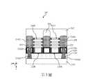
現在將參照圖式更加詳細地描述本揭露的各種態樣。對此,第1圖係根據本揭露實施例所示的流程圖,顯示形成半導體結構之方法100。方法100僅為一個範例,並非旨於將本揭露的內容限制為方法100中所明確說明的內容。對於方法的附加實施例,附加的操作可被提供於方法100之前、之中或是之後,且一些操作可被取代、消除或是移動。為使說明簡化,並非所有的操作均在本文中被詳細描述。下文結合第2圖至第9圖描述方法100,第2圖至第9圖是根據方法100的實施例,在不同製造階段之工作件200的局部截面圖。因為工作件200將在製造製程結束時被製造成半導體結構200,因此工作件200可根據前後文需要而被稱為半導體結構200。Various aspects of the disclosure will now be described in more detail with reference to the accompanying drawings. In this regard, FIG. 1 is a flowchart illustrating a
參照第1圖及第2圖,方法100包括方塊102,在方塊102中,工作件200被接收。參照第2圖,工作件200包括第一源極特徵214S1、第二源極特徵214S2、設置於第一源極特徵214S1與第二源極特徵214S2之間的汲極特徵214D、在第一源極特徵214S1與汲極特徵214D之間延伸的第一主動區208A、在第二源極特徵214S2與汲極特徵214D之間延伸的第二主動區208B、第一主動區208A上方的第一閘極結構210A、以及第二主動區208B上方的第二閘極結構210B。第一源極特徵214S1、第二源極特徵214S2、汲極特徵214D、第一主動區208A、第二主動區208B、第一閘極結構210A、以及第二閘極結構210B被設置在基板202上方。前側互連結構240被設置在第一源極特徵214S1、第二源極特徵214S2、汲極特徵214D、第一閘極結構210A、以及第二閘極結構210B上方。前側互連結構240包括複數金屬線以及接點通孔,並經由源極接點(第一源極接點222S1或第二源極接點222S2 ,視情況而定)和源極接點通孔(第一源極接點通孔232S1或第二源極接點通孔232S2,視情況而定),電性耦接至第一源極特徵214S1與第二源極特徵214S2中的每一者。Referring to FIGS. 1 and 2 , the
在一些實施例中,基板202包括矽(Si)。替代性地或是附加地,基板202包括另一種元素半導體,例如鍺(Ge);化合物半導體,例如碳化矽、砷化鎵、磷化鎵、磷化銦、砷化銦及/或銻化銦;合金半導體,例如矽鍺(SiGe)、GaAsP、AlInAs、AlGaAs、GaInAs、GaInP及/或GaInAsP;或者是其組合。在一些實施例中,基板202包括一或多種III-V族材料、一或多種II-VI族材料、或者是其組合。在一些實施例中,基板202為絕緣層上半導體(semiconductor-on-insulator)基板,例如絕緣層上矽(SOI)基板、絕緣層上矽鍺(SGOI)基板、或絕緣層上鍺(GeOI)基板。絕緣層上半導體基板可使用佈植氧分離(separation by implantation of oxygen, SIMOX)、晶圓接合(wafer bonding)、及/或其他合適的方法來製造。In some embodiments, the
在一些實施例中,第一主動區208A與第二主動區208B中的每一者包括複數奈米結構208,奈米結構208垂直地一者堆疊在另一者上方。複數奈米結構208作為多橋通道(multi-bridge -channel, MBC)電晶體的通道或通道構件。在這些實施例中,第一閘極結構210A包裹環繞(wrap around)第一主動區208A之複數奈米結構208中的每一者,而第二閘極結構210B包裹環繞第二主動區208B之複數奈米結構208中的每一者。在所繪實施例中,第一閘極結構210A控制第一MBC電晶體,而第二閘極結構210B控制第二MBC電晶體。由於其閘極結構圍繞通道區域,因此MBC電晶體亦可稱為環繞閘極電晶體(surrounding gate transistor, SGT)或閘極全環(gate-all-around, GAA)電晶體。MBC電晶體的奈米結構208可呈現奈米線、奈米片或其他奈米結構的形狀。通道區域的形狀也賦予了MBC電晶體替代性的名稱,例如奈米片電晶體或奈米線電晶體。在未明確展示的一些其他實施例中,第一主動區208A與第二主動區208B中的每一者包括鰭片結構,且形成在其上的電晶體為鰭式場效電晶體(fin-type field effect transistor, FinFET)。在一些實施例中,奈米結構208可由矽(Si)所形成。第一主動區208A與第二主動區208B形成自設置於基板202上方的磊晶層(epitaxial layer)堆疊以及基板202本身。磊晶層堆疊包括最終形成奈米結構208的第一半導體層,以及與第一半導體層交錯(interleaving)的第二半導體層。第二半導體層為犧牲層,作為犧牲層的第二半導體層被移除以釋放(release)第一半導體層來作為奈米結構208。在一些實施例中,第二半導體層可包括矽鍺(SiGe)。奈米結構208被插入了內部間隔特徵212,內部間隔特徵212將第一源極特徵214S1、第二源極特徵214S2以及汲極特徵214D,與第一閘極結構210A以及第二閘極結構210B分隔。內部間隔特徵212可以包括碳氮氧化矽(silicon oxycarbonitride)、氮化矽或是氮氧化矽。In some embodiments, each of the first
如第2圖所示,第一主動區208A在第一源極特徵214Sl與汲極特徵214D之間延伸,而第二主動區208B在第二源極特徵214S2與汲極特徵214D之間延伸。根據導電性型式(conductivity type),第一源極特徵214S1、第二源極特徵214S2以及汲極特徵214D可為n型,並且可包括摻雜有n型摻雜物的矽(Si),例如摻雜有磷(P)或砷(As);或者,第一源極特徵214S1、第二源極特徵214S2以及汲極特徵214D可包括摻雜有p型摻雜物的矽鍺(SiGe),例如摻雜有硼(B)或二氟化硼(BF2)。雖然第2圖中並未明確展示,但亦可在第一主動區208A以及第二主動區208B周圍形成隔離特徵。隔離特徵亦可被稱為淺溝槽隔離(shallow trench isolation, STI)特徵,可由一或多個介電層所形成,並且可使用化學氣相沉積(CVD)、次常壓化學氣相沉積(SACVD)或是原子層沉積(ALD)進行沉積。一或多個介電層可包括氧化矽、氮化矽、碳化矽、氮氧化矽、碳氮化矽、碳氧化矽、碳氮氧化矽及/或其組合。在一些實施例中,工作件200包括直接設置在汲極特徵214D下方的犧牲插塞206。犧牲插塞206可由與基板202之材料不同的半導體材料來形成。在一些實施例中,犧牲插塞206可包括矽鍺(SiGe)或鍺(Ge)。將在下文中進行描述的犧牲插塞206係作為後側汲極接點266的佔位符(placeholder)。犧牲插塞206可為未摻雜的或是未刻意摻雜的。As shown in FIG. 2, the first
第一閘極結構210A與第二閘極結構210B中的每一者包括界面層(interfacial layer)、界面層上方的閘極介電層、以及閘極介電層上方的閘極電極層。界面層包括氧化矽,並且可在預清潔(pre-clean)製程中形成。閘極介電層可包括高k值介電材料,高k值介電材料所具有的介電常數大於二氧化矽的介電常數,其中二氧化矽的介電常數為3.9。在一些實施例中,閘極介電層可包括氧化鈦(TiO2)、氧化鉿鋯(HfZrO)、氧化鉭(Ta2O5)、氧化鉿矽(HfSiO4)、氧化鋯(ZrO2)、氧化鋯矽(ZrSiO2)、氧化鑭(La2O3)、氧化鋁(Al2O3)、氧化鋯(ZrO)、氧化釔 (Y2O3)、SrTiO3(STO)、BaTiO3(BTO)、BaZrO、氧化鉿鑭(HfLaO)、氧化鑭矽(LaSiO)、氧化鋁矽(AlSiO)、氧化鉿鉭(HfTaO)、氧化鉿鈦(HfTiO)、(Ba,Sr)TiO3(BST)、氮化矽(SiN)、氮氧化矽(SiON)、其組合、或是其他合適的材料。閘極電極層可包括多個薄層,例如具有經過選擇之功函數以提高裝置性能的金屬層(功函數金屬層)、襯墊層(liner layer)、膠合層(glue layer)、阻擋層(blocking layer)、以及金屬填充物的各種組合。舉例來說,閘極電極層可包括氮化鈦(TiN)、鈦鋁(TiAl)、氮化鈦鋁(TiAlN)、氮化鉭(TaN)、鉭鋁(TaAl)、氮化鉭鋁(TaAlN)、碳化鉭鋁(TaAlC)、碳氮化鉭 (TaCN)、鋁(Al)、鎢(W)、鎳(Ni)、鈦(Ti)、釕(Ru)、鈷(Co)、鉑(Pt)、碳化鉭(TaC)、氮化鉭矽(TaSiN)、銅(Cu)、其他耐火金屬(refractory metal)、或是其他合適的金屬材料、或其組合。一或多個閘極間隔物211沿著第一閘極結構210A或第二閘極結構210B的側壁沿著最頂部之奈米結構208設置。多個閘極間隔物211中的一者可包括氮化矽、碳氮氧化矽或氮氧化矽。因為它們位於最頂部之奈米結構208上方,因此一或多個閘極間隔物211亦可被稱為頂部間隔物。Each of the
工作件200進一步包括位在第一源極特徵214Sl、第二源極特徵214S2以及汲極特徵214D中的每一者上方的接觸蝕刻停止層(contact etch stop layer, CESL)216與第一層間介電(interlayer dielectric, ILD)層218。接觸蝕刻停止層216可包括氮化矽、氮氧化矽及/或本技術領域已知的其他材料。第一ILD層218可包括的材料例如正矽酸乙酯(tetraethylorthosilicate, TEOS)氧化物、未摻雜之矽酸鹽玻璃或摻雜之氧化矽,例如硼磷矽酸鹽玻璃(borophospho- silicate glass, BPSG)、熔融石英玻璃(fused silica glass, FSG)、磷矽酸鹽玻璃(phosphosilicate glass, PSG)、硼摻雜之石英玻璃 (boron doped silica glass, BSG)、及/或其他合適的介電材料。第一源極接點222S1延伸穿過接觸蝕刻停止層216以及第一ILD層218以經由矽化物特徵220耦接到第一源極特徵214S1。第二源極接點222S2延伸穿過接觸蝕刻停止層216以及第一ILD層218以經由矽化物特徵220耦接到第二源極特徵214S2。第一源極接點222S1以及第二源極接點222S2可包括釕(Ru)、銅(Cu)、鎳(Ni)、鈷(Co)、鎢(W)。矽化物特徵220可包括矽化鈦(TiSi)、氮化矽鈦(TiSiN)、矽化鉭(TaSi)、矽化鎢(WSi)、矽化鈷(CoSi)或矽化鎳(NiSi)。The
工作件200進一步包括位在第一源極接點222Sl、第一ILD層218、接觸蝕刻停止層216、以及第二源極接點222S2上方的第一蝕刻停止層(ESL)224。第一ESL 224可具有與接觸蝕刻停止層216相似的組成。第二層間介電(ILD)層226被設置在第一ESL 224上方。第二ILD層226在組成方面可類似於第一ILD層218。第一源極接點通孔232S1延伸穿過第二ILD層226以及第一ESL 224,以耦接至第一源極接點222S1。第二源極接點通孔232S2延伸穿過第二ILD層226以及第一ESL 224,以耦接至第二源極接點222S2。第一源極接點通孔232S1以及第二源極接點通孔232S2可包括釕(Ru)、銅(Cu)、鎳(Ni)、鈷(Co)或鎢(W),並且亦可包括由金屬氮化物形成的阻障層(barrier layer),例如由氮化鈦或氮化鉭所形成的阻障層。The
參照第1圖及第2圖,方法100包括方塊104,在方塊104中,前側互連結構240被形成在工作件200上方。在一些實施例中,前側互連結構240可包括複數金屬間介電(intermetal dielectric, IMD)層,以及包括每個IMD層中的複數金屬線或接點通孔。在一些實施例中,IMD層與第一ILD層218可共享相似的組成。每個IMD層中的金屬線以及接點通孔可由金屬形成,例如由鋁(Al)、鎢(W)、釕(Ru)或銅(Cu)所形成。在一些實施例中,金屬線與接點通孔可被阻障層所襯墊,以將金屬線及接點通孔與IMD層隔離並防止電遷移(electro-migration)。阻障層可包括氮化鈦或氮化鉭。前側互連結構240中的金屬線耦接到第一源極接點通孔232S1以及第二源極接點通孔232S2。Referring to FIGS. 1 and 2 , the
參照第1圖、第3圖及第4圖,方法100包括方塊106,在方塊106中,工作件200被上下翻轉(flip)。在一些實施例中,承載基板(未圖示)可被接合到前側互連結構240,且工作件200被上下翻轉使得基板202的後側指向上方,如第3圖所示。承載基板可由半導體材料(例如:矽)、藍寶石、玻璃、聚合材料、或是其他合適的材料形成。參照第4圖,工作件200的後側被平坦化直到犧牲插塞206的頂部表面與基板202的頂部表面共平面。儘管並未顯示,但隔離特徵也曝露在平坦的頂部表面中。Referring to FIGS. 1 , 3 , and 4 , the
參照第1圖以及第5圖至第7圖,方法100包括方塊108,在方塊108中,後側汲極接點266被形成以耦接至汲極特徵214D。方塊108中的操作包括移除基板202(顯示於第5圖)、沉積襯墊260(顯示於第6圖)、沉積後側介電層262(顯示於第6圖)、以及用後側汲極接點266替換犧牲插塞206(顯示於第7圖)。參照第5圖,因為犧牲插塞206與基板202由不同的材料所形成,因此可以使用選擇性乾式蝕刻製程或選擇性濕式蝕刻製程來選擇性地移除基板202。在移除基板202之後,使用ALD或CVD在工作件200的後側上方沉積襯墊260,如第6圖所示。在一些實施例中,襯墊260可包括氮化矽。接著使用自旋塗佈(spin-on coating)、CVD或電漿增強型CVD(PECVD)在襯墊260上方沉積後側介電層262。在沉積襯墊260以及後側介電層262之後,執行諸如CMP製程的平坦化製程,以提供平坦的後側表面。在平坦化製程之後,犧牲插塞206被嵌入後側介電層262與隔離特徵之中。犧牲插塞206接著被以後側汲極接點266所取代。Referring to FIG. 1 and FIGS. 5-7 , the
在範例性的製程中,犧牲插塞206被選擇性地移除來形成後側汲極開口以曝露汲極特徵214D。接著,後側的矽化物層264被形成在汲極特徵214D之曝露表面上方,且後側汲極接點266被沉積在矽化物層264上方。可使用選擇性濕式蝕刻製程或選擇性乾式蝕刻製程來執行犧牲插塞206的選擇性移除。為了降低汲極特徵214D與後側汲極接點266之間的接觸電阻,矽化物層264可被形成在後側汲極開口中之汲極特徵214D的曝露表面上。矽化物層264可包括矽化鈦(TiSi)、氮化矽鈦(TiSiN)、矽化鉭(TaSi)、矽化鎢(WSi)、矽化鈷(CoSi)或是矽化鎳(NiSi)。在形成矽化物層264之後,金屬填充層可被沉積到後側汲極開口中,以形成後側汲極接點266,如第7圖所示。金屬填充層可以包括鋁(Al)、銠(Rh)、釕(Ru)、銅(Cu)、銥(Ir)或是鎢(W)。可接著進行諸如CMP製程的平坦化製程,以移除多餘的材料並提供平坦的頂部表面。後側汲極接點266與矽化物層264直接接觸,且矽化物層264與汲極特徵214D直接接觸。換句話說,矽化物層264被夾設(sandwich)於汲極特徵214D與後側汲極接點266之間。In an exemplary process, the
參照第1圖及第7圖,方法100包括方塊110,在方塊110中,第一後側金屬線270被形成在後側汲極接點266上方。第一後側金屬線270被形成在第三ILD層268之中。在範例性的製程中,第三ILD層268包括與第一ILD層218相似的組成,且被沉積在工作件200的後側上方,包括後側介電層262、隔離特徵、襯墊260以及後側汲極接點266的上方。接著,可在第三ILD層268中圖案化(pattern)出溝槽。然後,阻障層以及金屬填充材料被沉積到溝槽中,以在後側汲極接點266上方形成第一後側金屬線270。在一些實施例中,第一後側金屬線270中的阻障層可包括氮化鈦、氮化鉭、氮化鈷、氮化鎳或是氮化鎢,而第一後側金屬線270中的金屬填充材料可包括鈦(Ti)、釕(Ru)、銅(Cu)、鎳(Ni)、鈷(Co)、鎢(W)、鉭(Ta)或是鉬(Mo)。可使用物理氣相沉積(PVD)、CVD、ALD或無電電鍍(electroless plating)來沉積阻障層以及金屬填充層。可執行諸如CMP製程的平坦化製程,以移除第三ILD層268上方的多餘材料。Referring to FIGS. 1 and 7 , the
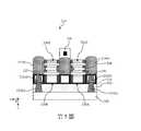
參照第1圖及第8圖,方法100包括方塊112,在方塊112中,儲存元件300被形成在第一後側金屬線270上方。在一些實施例中,儲存元件300為MRAM儲存元件或MRAM單元,且包括MTJ結構。在範例性的製程中,第二蝕刻停止層(ESL)272、保護層274以及介電層276被形成在工作件200的後側上方。第二ESL 272可包括氮化矽,保護層274可包括氧化鋁、氮化鋁或是氮氧化鋁,而介電層276可包括碳化矽(SiC)、氮氧化矽(SiON)、氮化矽(SiN)、二氧化矽、TEOS、低k值介電質、FSG、PSG、BPSG等,及/或其組合。仍舊參照第8圖。頂部電極通孔(TEVA)278被形成以延伸穿過第二ESL 272、保護層274以及介電層276。頂部電極通孔278可包括氮化鈦(TiN)、氮化鉭(TaN)、鈦(Ti)、鉭(Ta)、鉑(Pt)、釕(Ru)、鎢(W)、鋁(Al)、銅(Cu)、類似的材料、及/或其組合。Referring to FIGS. 1 and 8 , the
接著,儲存元件300被形成在頂部電極通孔278上。儲存元件300之放大截面圖顯示於第10圖中。在一些實施例中,儲存元件300包括與頂部電極通孔278接觸的頂部電極302、頂部電極302上方的釘扎層304、釘扎層304上方的穿隧阻障層306、穿隧阻障層上方的自由層308、以及底部電極310。頂部電極302以及底部電極310可包括鈦(Ti)、鉭(Ta)、鉑(Pt)、釕(Ru)、鎢(W)、鋁(Al)、銅(Cu)、TiN、TaN、類似的材料、及/或其組合。儘管在第10圖中,底部電極310看起來是在頂部電極302上方,但在工作件200被翻轉之後,頂部電極302將位於頂部。釘扎層304可包括鈷鐵硼(CoFeB)、CoFeTa、NiFe、Co、CoFe、CoPt、Ni與Co和Fe的合金、鉑錳(PtMn)、銥錳(IrMn)、銠錳(RhMn)、鐵錳(FeMn)或是OsMn。穿隧阻障層306可包括氧化鎂(MgO)、氧化鋁(Al2O3)、氮化鋁(AlN)、氮氧化鋁(AlON)、氧化鉿(HfO2)或是氧化鋯(ZrO2)。自由層308可包括鈷、鎳、鐵或硼。釘扎層304、穿隧阻障層306與自由層308構成磁穿隧接面(MTJ)結構。儲存元件300的側壁由間隔物281所襯墊。間隔物281包括氮化矽、碳化矽、碳氮氧化矽或碳氧化矽。在形成儲存元件300之後,底部電極通孔(BEVA) 282被形成在底部電極310上方以耦接底部電極310。與頂部電極通孔(TEVA)278相同,底部電極通孔(BEVA)282可包括氮化鈦(TiN)、氮化鉭(TaN)、鈦(Ti)、鉭(Ta)、鉑(Pt)、釕(Ru)、鎢(W)、鋁(Al)、銅(Cu)、類似的材料、及/或其組合。包括底部電極通孔(BEVA)282的儲存元件300被設置在第四ILD層284中。第四ILD層284的組成可類似於第一ILD層218的組成。Next, the
參照第1圖及第8圖,方法100包括方塊114,在方塊114中,第二後側金屬線288被形成在儲存元件300上方。第二後側金屬線288被形成在第五ILD層286之中。在範例性的製程中,第五ILD層286包括與第一ILD層218相似的組成,並且可被沉積在第四ILD層284與底部電極通孔(BEVA)282上方。接著,可在第五ILD層286中圖案化出溝槽。然後,阻障層以及金屬填充材料被沉積到溝槽中,以直接在底部電極通孔(BEVA)282上方形成第二後側金屬線288。在一些實施例中,第二後側金屬線288中的阻障層可包括氮化鈦、氮化鉭、氮化鈷、氮化鎳或是氮化鎢,而第二後側金屬線288中的金屬填充材料可包括鈦(Ti)、釕(Ru)、銅(Cu)、鎳(Ni)、鈷(Co)、鎢(W)、鉭(Ta)或是鉬(Mo)。可使用PVD、CVD、ALD或是無電電鍍來沉積阻障層以及金屬填充層。可執行諸如CMP製程的平坦化製程,以移除第五ILD層286上方的多餘材料。第一後側金屬線270、儲存元件300以及第二後側金屬線288位於後側互連結構290之中。前側互連結構240與後側互連結構290被形成在FEOL特徵的不同側上,其中FEOL特徵例如第一源極特徵214S1、第二源極特徵214S2、汲極特徵214D、第一閘極結構210A、第二閘極結構210B、第一主動區208A、以及第二主動區208B。Referring to FIGS. 1 and 8 , the
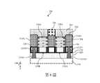
第9圖顯示了在執行方塊114中的操作之後,再次上下翻轉的工作件200。如第9圖所示,第一主動區208A在第一源極特徵214S1與汲極特徵214D之間延伸,而第二主動區208B在汲極特徵214D與第二源極特徵214S2之間延伸。第一閘極結構210A包裹環繞第一主動區208A中的每個奈米結構208,而第二閘極結構210B包裹環繞第二主動區208B中的每個奈米結構208。第一源極特徵214S1經由第一源極接點222S1以及第一源極接點通孔232S1耦接到前側互連結構240。第二源極特徵214S2經由第二源極接點222S2以及第二源極接點通孔232S2耦接到前側互連結構240。後側汲極接點266自汲極特徵214D向下延伸穿過後側介電層262。後側汲極接點266藉由襯墊260而與後側介電層262間隔開來。汲極特徵214D經由後側汲極接點266耦接到後側互連結構290。具體來說,後側汲極接點266被設置在第一後側金屬線270上,第一後側金屬線270耦接到頂部電極通孔(TEVA)278。頂部電極通孔(TEVA) 278耦接到儲存元件300的頂部電極。儲存元件300的底部電極310耦接到底部電極通孔(BEVA)282。底部電極通孔(BEVA)282被設置在第二後側金屬線288上,或是電性耦接到第二後側金屬線288。FIG. 9 shows the
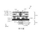
第11圖表示第9圖在後側互連結構290中的儲存元件300的操作方面的示意圖。第二後側金屬線288作為位元線(BL)。前側互連結構240包括藉由接點通孔耦接在一起的複數金屬層。舉例來說,前側互連結構240包括第一金屬層M0、第二金屬層M1以及第三金屬層M2。第一金屬層M0中的金屬線242被設置在第一源極接點通孔232S1與第二源極接點通孔232S2上,並與第一源極接點通孔232S1和第二源極接點通孔232S2耦接。第三金屬層M2中的金屬線250被設置在金屬線242上方,並且經由第二金屬層M1中的接點通孔244、接點通孔248以及金屬線245耦接到金屬線242。金屬線242與金屬線250共同作為共用源極線(CSL)以降低線電阻(line resistance)。金屬線246電性耦接至第一閘極結構210A與第二閘極結構210B兩者,以作為字元線(WL)。FIG. 11 shows a schematic diagram of FIG. 9 in terms of the operation of the
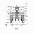
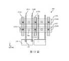
各種連接與選路可藉由第12圖至第14圖中所示的佈局來理解。第12圖顯示了源極接點、源極接點通孔、第一金屬層(M0)、以及第一金屬層(M0)與第二金屬層(M1)之間的接點通孔的局部俯視佈局圖。如第12圖所示,第一主動區208A以及第二主動區208B沿著X方向縱向延伸,且代表性地表示為連續主動區2080。諸如第一閘極結構210A與第二閘極結構210B的閘極結構,沿著Y方向縱向延伸。兩個相鄰源極接點之間的每一對閘極結構,經由閘極接點通孔233連接到第一金屬層M0中的金屬特徵243,金屬特徵243將電性耦接至第二金屬層M1中的金屬線246(WL)。第一源極接點222S1與第二源極接點222S2中的每一者,沿著Y方向縱向延伸以連接源極特徵的陣列,例如第一源極特徵214S1以及第二源極特徵214S2。第一源極接點222S1經由第一源極接點通孔232S1耦接到第一金屬層M0中的導線,而第二源極接點222S2經由第二源極接點通孔232S2耦接到第一金屬層M0中的導線。接點通孔244連接第一金屬層(M0)中的金屬線242與第二金屬層(M1)中的金屬線245。當沿著Z方向從頂部觀察時,第一源極接點通孔232S1、第二源極接點通孔232S2與接點通孔244可以是等邊的(equilateral)。在一些實施例中,第一源極接點通孔232S1或第二源極接點通孔232S2所包括的X/Y方向尺寸,介於約10nm與約16nm之間。每個接點通孔244所包括的X-Y方向尺寸,介於約10nm與約20nm之間。包括第一閘極結構210A及第二閘極結構210B的閘極結構以間距P設置,間距P可介於約30nm與約65nm之間。第一源極接點通孔232S1(或是第二源極接點通孔232S2)之尺寸對間距P的比值可介於0.3與約0.5之間。這個比值並非微不足道的。當此比值小於0.3時,源極接點通孔的電阻可能會增加,並因此影響裝置性能。當此比值大於0.5時,形成源極接點通孔的製程窗口可能會變得太小,且源極接點通孔與相鄰之閘極結構之間的電容可能會增加,並因而影響裝置性能。The various connections and routings can be understood by the layouts shown in Figures 12-14. Figure 12 shows the source contact, the source contact via, the first metal layer (M0), and a portion of the contact via between the first metal layer (M0) and the second metal layer (M1) Overlook layout. As shown in FIG. 12 , the first
接著參照第13圖,第一金屬層M0中的金屬特徵243經由接點通孔249耦接到金屬線246(WL)。應注意的是,金屬特徵243以及接點通孔249位於週邊區域中。金屬線246(WL)被直接設置於第一源極接點通孔232S1、第一源極接點222S1以及第一源極特徵214S1(顯示於第9圖)上方。第二金屬層M1中的金屬線245沿著Y方向延伸,且平行於金屬線246。金屬線245被直接設置在接點通孔248以及汲極特徵214D(顯示於第9圖)上方。金屬線245及246被以介於30nm與約60nm之間的間距進行設置。在一些實施例中,金屬線245及246中的每一者所包括的X方向寬度,介於約14nm與30nm之間。因為接點通孔248位於源極接點通孔(例如:第一源極接點通孔232S1和第二源極接點通孔232S2)以及接點通孔244上方的金屬層中,因此接點通孔248可具有更大的截面面積。在一些實施例中,接點通孔248的X/Y方向尺寸可介於約10nm與約24nm之間。Referring next to FIG. 13 , the
最後參照第14圖,第14圖為後側互連結構290的後側俯視佈局圖。後側汲極接點266的頂部投影面積類似於汲極特徵214D的頂部投影面積。第一後側金屬線270中的每一者類似於島嶼,且被實施以擴大後側汲極接點266的接觸面積。垂直地,第一後側金屬線270的一部分與第一閘極結構210A以及第二閘極結構210B垂直地部分重疊。儲存元件300被形成在第一後側金屬線270上方。第二後側金屬線288沿著X方向在儲存元件與第一後側金屬線270上方延伸。第二後側金屬線288在連續主動區2080上方延伸,且被用作位元線(BL)。Finally, referring to FIG. 14 , FIG. 14 is a rear top plan layout diagram of the
仍舊參照第14圖,後側汲極接點266包括沿著X方向的第一寬度W1。在一些實施例中,第一寬度W1介於約5nm與約30nm之間。後側汲極接點266亦包括介於約20nm與約40nm之間的Y方向尺寸,Y方向尺寸基本上由主動區2080的Y方向尺寸來定義。儲存元件300之最寬的部分包括沿著X方向的第二寬度W2。在一些實施例中,第二寬度W2介於約20nm與約60nm之間。儲存元件300的最大Y方向尺寸可類似於第二寬度W2。在一些實施例中,儲存元件300之第二寬度與Y方向尺寸的比值,介於約1與1.2之間。第一後側金屬線270包括沿著X方向的第三寬度W3。在一些實施例中,第三寬度W3可介於約30nm與約75nm之間。根據本揭露,第三寬度W3大於第二寬度W2,以確保頂部電極通孔(TEVA)278在第一後側金屬線270上良好的著陸(landing)。Still referring to FIG. 14 , the
本揭露實施例提供了許多優點。如第15圖所示,藉由將儲存元件以及儲存元件的連接特徵從前側互連結構移動到後側互連結構,裝置的面積可減少約15%至約25%,例如20%。前側互連結構中的空閒空間可被利用來整合附加的後段製程特徵、降低選路密度、或是減少裝置尺寸。Embodiments of the present disclosure provide many advantages. As shown in FIG. 15, by moving the storage element and the connection features of the storage element from the front side interconnect structure to the back side interconnect structure, the area of the device can be reduced by about 15% to about 25%, such as 20%. The free space in the front-side interconnect structure can be utilized to integrate additional back-end-of-line features, reduce routing density, or reduce device size.
在一個範例性態樣中,本揭露直指一種半導體結構。上述半導體結構包括源極特徵以及汲極特徵、源極特徵與汲極特徵之間的主動區、主動區上方的閘極結構、設置於源極特徵以及汲極特徵還有閘極結構上方的前側互連結構、設置於源極特徵以及汲極特徵還有閘極結構下方的後側互連結構、以及設置於後側互連結構之中的儲存元件。In an exemplary aspect, the present disclosure is directed to a semiconductor structure. The semiconductor structure includes a source feature and a drain feature, an active region between the source feature and the drain feature, a gate structure above the active region, a front side disposed above the source feature, the drain feature and the gate structure The interconnection structure, the backside interconnection structure disposed under the source feature, the drain feature and the gate structure, and the storage element disposed in the backside interconnection structure.
在一些實施例中,儲存元件為一磁阻式隨機存取(MRAM)元件。In some embodiments, the storage element is a magnetoresistive random access (MRAM) element.
在一些實施例中,主動區包括在源極特徵與汲極特徵之間延伸的複數奈米結構。In some embodiments, the active region includes a complex of nanostructures extending between the source and drain features.
在一些實施例中,閘極結構包裹環繞複數奈米結構中的每一者。In some embodiments, a gate structure wraps around each of the plurality of nanostructures.
在一些實施例中,前側互連結構耦接至源極特徵以及閘極結構,且後側互連結構耦接至儲存元件。In some embodiments, the front side interconnect structure is coupled to the source features and the gate structure, and the back side interconnect structure is coupled to the storage element.
在一些實施例中,前側互連結構經由源極接點以及設置於源極接點上方的源極接點通孔耦接至源極特徵。In some embodiments, the frontside interconnect structure is coupled to the source feature via a source contact and a source contact via disposed over the source contact.
在一些實施例中,後側互連結構經由後側汲極接點耦接至汲極特徵。In some embodiments, the backside interconnect structure is coupled to the drain feature via a backside drain contact.
在一些實施例中,後側互連結構更包括設置於後側汲極接點與儲存元件之間的第一金屬線,以及包括設置於儲存元件下方的第二金屬線,使得儲存元件被設置於第一金屬線與第二金屬線之間。In some embodiments, the backside interconnection structure further includes a first metal line disposed between the backside drain contact and the storage element, and includes a second metal line disposed under the storage element, so that the storage element is disposed Between the first metal line and the second metal line.
在一些實施例中,儲存元件包括設置於第二金屬線上的底部電極通孔、設置於底部電極通孔上的底部電極、設置於底部電極上方的頂部電極、夾設於底部電極與頂部電極之間的磁穿隧接面(MTJ)層、以及設置於頂部電極與第一金屬線之間的頂部電極通孔。In some embodiments, the storage element includes a bottom electrode via hole disposed on the second metal line, a bottom electrode disposed on the bottom electrode via hole, a top electrode disposed above the bottom electrode, and interposed between the bottom electrode and the top electrode. A magnetic tunnel junction (MTJ) layer between the top electrodes and a top electrode via hole disposed between the top electrode and the first metal line.
在另一個範例性態樣中,本揭露直指一種半導體結構。上述半導體結構包括第一源極特徵以及第二源極特徵、設置於第一源極特徵與第二源極特徵之間的汲極特徵、在第一源極特徵與汲極特徵之間延伸的第一主動區、在汲極特徵與第二源極特徵之間延伸的第二主動區、位於第一主動區上方的第一閘極結構、位於第二主動區上方的第二閘極結構、設置於第一源極特徵與第二源極特徵和第一閘極結構以及第二閘極結構上方,並且電性耦接至第一源極特徵與第二源極特徵和第一閘極結構以及第二閘極結構的前側互連結構、設置於第一源極特徵與第二源極特徵和汲極特徵還有第一閘極結構以及第二閘極結構下方的後側互連結構、以及設置於後側互連結構之中的儲存元件。後側互連結構電性耦接至汲極特徵。In another exemplary aspect, the present disclosure is directed to a semiconductor structure. The above semiconductor structure includes a first source feature and a second source feature, a drain feature disposed between the first source feature and the second source feature, a drain feature extending between the first source feature and the drain feature a first active region, a second active region extending between the drain feature and the second source feature, a first gate structure over the first active region, a second gate structure over the second active region, disposed over the first source feature and the second source feature and the first gate structure and the second gate structure, and electrically coupled to the first source feature, the second source feature and the first gate structure and the front side interconnect structure of the second gate structure, the back side interconnect structure disposed under the first source feature and the second source feature and the drain feature and the first gate structure and the second gate structure, and a storage element disposed in the backside interconnection structure. The backside interconnect structure is electrically coupled to the drain feature.
在一些實施例中,儲存元件為磁阻式隨機存取(MRAM)元件。In some embodiments, the storage element is a magnetoresistive random access (MRAM) element.
在一些實施例中,第一主動區包括一者堆疊在另一者上方的複數第一奈米結構,而第二主動區包括一者堆疊在另一者上方的複數第二奈米結構。In some embodiments, the first active region includes a plurality of first nanostructures stacked one on top of the other, and the second active region includes a plurality of second nanostructures stacked one on top of the other.
在一些實施例中,第一閘極結構包裹環繞複數第一奈米結構中的每一者,而第二閘極結構包裹環繞複數第二奈米結構中的每一者。In some embodiments, the first gate structure wraps around each of the plurality of first nanostructures, and the second gate structure wraps around each of the plurality of second nanostructures.
在一些實施例中,前側互連結構經由第一源極接點以及設置於第一源極接點上方的第一源極接點通孔耦接至第一源極特徵、前側互連結構經由第二源極接點以及設置於第二源極接點上方的第二源極接點通孔耦接至第二源極特徵、以及後側互連結構經由後側汲極接點耦接至汲極特徵。In some embodiments, the front-side interconnect structure is coupled to the first source feature via the first source contact and the first source contact via disposed above the first source contact, the front-side interconnect structure is coupled to the first source feature via The second source contact and the second source contact via disposed over the second source contact are coupled to the second source feature, and the backside interconnect structure is coupled to the second source feature via the backside drain contact. Drain characteristics.
在一些實施例中,第一源極接點設置於第一源極特徵上方,並自第一源極特徵向上延伸、第二源極接點設置於第二源極特徵上方,並自第二源極特徵向上延伸、以及後側汲極接點設置於汲極特徵下方,並自汲極特徵向下延伸。In some embodiments, a first source contact is disposed over and extends upward from the first source feature, and a second source contact is disposed over the second source feature and extends upward from the second source feature. The source feature extends upward, and the backside drain contact is disposed below the drain feature and extends downward from the drain feature.
在一些實施例中,後側互連結構更包括設置於後側汲極接點與儲存元件之間的第一金屬線,以及包括設置於儲存元件下方的第二金屬線,使得儲存元件被設置於第一金屬線與第二金屬線之間。In some embodiments, the backside interconnection structure further includes a first metal line disposed between the backside drain contact and the storage element, and includes a second metal line disposed under the storage element, so that the storage element is disposed Between the first metal line and the second metal line.
在一些實施例中,儲存元件包括設置於第二金屬線上的底部電極通孔、設置於底部電極通孔上的底部電極、設置於底部電極上方的頂部電極、夾設於底部電極與頂部電極之間的磁穿隧接面(MTJ)層、以及設置於頂部電極與第一金屬線之間的頂部電極通孔。In some embodiments, the storage element includes a bottom electrode via hole disposed on the second metal line, a bottom electrode disposed on the bottom electrode via hole, a top electrode disposed above the bottom electrode, and interposed between the bottom electrode and the top electrode. A magnetic tunnel junction (MTJ) layer between the top electrodes and a top electrode via hole disposed between the top electrode and the first metal line.
在又一個範例性態樣中,本揭露直指一種半導體結構的形成方法。上述半導體結構的形成方法包括在基板上方形成一電晶體。上述電晶體包括源極特徵、汲極特徵、夾設於源極特徵與汲極特徵之間的主動區、以及位於主動區上方的閘極結構。上述半導體結構的形成方法更可以包括在源極特徵上方形成源極接點通孔,其中源極接點通孔電性耦接至源極特徵、形成前側互連結構,前側互連結構設置在源極接點通孔上方,且電性耦接至源極接點通孔、在形成前側互連結構之後形成後側汲極接點,後側汲極接點電性耦接至汲極特徵且遠離前側互連結構、以及形成耦接至後側汲極接點的後側互連結構。後側互連結構包括儲存元件。In yet another exemplary aspect, the present disclosure is directed to a method of forming a semiconductor structure. The method for forming the semiconductor structure includes forming a transistor above the substrate. The transistor includes a source feature, a drain feature, an active region sandwiched between the source feature and the drain feature, and a gate structure above the active region. The method for forming the above semiconductor structure may further include forming a source contact via above the source feature, wherein the source contact via is electrically coupled to the source feature to form a front-side interconnection structure, and the front-side interconnection structure is disposed on above and electrically coupled to the source contact via, a backside drain contact is formed after forming the frontside interconnect structure, and the backside drain contact is electrically coupled to the drain feature and away from the front-side interconnect structure, and form a back-side interconnect structure coupled to the back-side drain contact. The backside interconnect structure includes storage elements.
在一些實施例中,上述半導體結構的形成方法更可以包括在形成後側汲極接點之前翻轉上述基板,使得後側互連結構位在電晶體之上。In some embodiments, the method for forming the above-mentioned semiconductor structure may further include flipping the above-mentioned substrate before forming the back-side drain contact, so that the back-side interconnection structure is located on the transistor.
在一些實施例中,儲存元件為磁阻式隨機存取(MRAM)元件。In some embodiments, the storage element is a magnetoresistive random access (MRAM) element.
前述內文概述多項實施例之特徵,如此可使於本技術領域中具有通常知識者更佳地瞭解本揭露之態樣。本技術領域中具有通常知識者應當理解他們可輕易地以本揭露為基礎設計或修改其他製程及結構,以完成相同之目的及/或達到與本文介紹之實施例或範例相同之優點。本技術領域中具有通常知識者亦需理解,這些等效結構並未脫離本揭露之精神及範圍,且在不脫離本揭露之精神及範圍之情況下,可對本揭露進行各種改變、置換以及變更。The foregoing text summarizes features of various embodiments so that those skilled in the art can better understand aspects of the present disclosure. Those skilled in the art should understand that they can easily design or modify other processes and structures based on the present disclosure to achieve the same purpose and/or achieve the same advantages as the embodiments or examples introduced herein. Those with ordinary knowledge in the technical field also need to understand that these equivalent structures do not depart from the spirit and scope of the present disclosure, and that various changes, substitutions and changes can be made to the present disclosure without departing from the spirit and scope of the present disclosure .
100:方法 102~114:方塊 200:工作件 202:基板 206:犧牲插塞 208:奈米結構 208A:第一主動區 208B:第二主動區 210A:第一閘極結構 210B:第二閘極結構 211:閘極間隔物 212:內部間隔特徵 214S1:第一源極特徵 214S2:第二源極特徵 214D:汲極特徵 216:接觸蝕刻停止層 218:第一ILD層 220:矽化物特徵 222S1:第一源極接點 222S2:第二源極接點 224:第一蝕刻停止層 226:第二ILD層 232S1:第一源極接點通孔 232S2:第二源極接點通孔 240:前側互連結構 260:襯墊 262:後側介電層 264:矽化物層 266:後側汲極接點 268:第三ILD層 270:第一後側金屬線 272:第二ESL 274:保護層 276:介電層 278:頂部電極通孔 281:間隔物 282:底部電極通孔 284:第四ILD層 286:第五ILD層 288:第二後側金屬線 290:後側互連結構 300:儲存元件 302:頂部電極 304:釘扎層 306:穿隧阻障層 308:自由層 310:底部電極 242:金屬線 244:接點通孔 245:金屬線 246:金屬線 248:接點通孔 250:金屬線 M0:第一金屬層 M1:第二金屬層 M2:第三金屬層 233:閘極接點通孔 243:金屬特徵 2080:連續主動區 249:接點通孔 P:間距 W1:第一寬度 W2:第二寬度 W3:第三寬度100: method 102~114: block 200: work pieces 202: Substrate 206: sacrificial plug 208:Nanostructure 208A: The first active zone 208B: The second active area 210A: first gate structure 210B: second gate structure 211: gate spacer 212:Internal interval feature 214S1: First source characteristic 214S2: Second source characteristic 214D: drain characteristics 216: contact etch stop layer 218: The first ILD layer 220: Silicide Features 222S1: The first source contact 222S2: Second source contact 224: the first etching stop layer 226: Second ILD layer 232S1: First source contact via 232S2: Second source contact via 240: Front side interconnection structure 260: pad 262: rear side dielectric layer 264: Silicide layer 266: Rear side drain contact 268: The third ILD layer 270: the first rear metal wire 272:Second ESL 274: protective layer 276: dielectric layer 278: Top electrode through hole 281: spacer 282: Bottom electrode through hole 284: The fourth ILD layer 286: Fifth ILD layer 288: Second rear metal wire 290: rear side interconnection structure 300: storage element 302: top electrode 304: Pinning layer 306: Tunneling barrier layer 308: free layer 310: bottom electrode 242: metal wire 244: Contact through hole 245: metal wire 246: metal wire 248: Contact through hole 250: metal wire M0: first metal layer M1: second metal layer M2: The third metal layer 233: Gate contact through hole 243:Metal Features 2080: continuous active area 249: Contact through hole P: Pitch W1: first width W2: second width W3: third width
本揭露自後續實施方式及附圖可更佳理解。須強調的是,依據產業之標準作法,各種特徵並未按比例繪製,並僅用於說明之目的。事實上,各種特徵之尺寸可能任意增加或減少以清楚論述。 第1圖係根據本揭露一或多個態樣所示,在後側互連結構中具有儲存元件之半導體結構的形成方法的流程圖。 第2圖係根據本揭露一或多個態樣所示,在根據第1圖之方法的製造製程期間,工作件的局部截面圖。 第3圖係根據本揭露一或多個態樣所示,在根據第1圖之方法的製造製程期間,工作件的局部截面圖。 第4圖係根據本揭露一或多個態樣所示,在根據第1圖之方法的製造製程期間,工作件的局部截面圖。 第5圖係根據本揭露一或多個態樣所示,在根據第1圖之方法的製造製程期間,工作件的局部截面圖。 第6圖係根據本揭露一或多個態樣所示,在根據第1圖之方法的製造製程期間,工作件的局部截面圖。 第7圖係根據本揭露一或多個態樣所示,在根據第1圖之方法的製造製程期間,工作件的局部截面圖。 第8圖係根據本揭露一或多個態樣所示,在根據第1圖之方法的製造製程期間,工作件的局部截面圖。 第9圖係根據本揭露一或多個態樣所示,在根據第1圖之方法的製造製程期間,工作件的局部截面圖。 第10圖係根據本揭露一或多個態樣所示,儲存元件的放大局部截面圖。 第11圖係根據本揭露一或多個態樣所示,半導體結構中之互連特徵的示意性截面圖。 第12圖係根據本揭露一或多個態樣所示,半導體結構中的俯視佈局圖。 第13圖係根據本揭露一或多個態樣所示,半導體結構中的俯視佈局圖。 第14圖係根據本揭露一或多個態樣所示,半導體結構中的俯視佈局圖。 第15圖根據本揭露一或多個態樣顯示了藉由在後側互連結構中包括儲存元件所帶來的面積降低。The present disclosure can be better understood from the subsequent description and drawings. It is emphasized that, in accordance with the standard practice in the industry, various features are not drawn to scale and are used for illustration purposes only. In fact, the dimensions of the various features may be arbitrarily increased or decreased for clarity of discussion. FIG. 1 is a flowchart of a method for forming a semiconductor structure with storage elements in a backside interconnection structure according to one or more aspects of the present disclosure. FIG. 2 is a partial cross-sectional view of a workpiece during a fabrication process according to the method of FIG. 1 , according to one or more aspects of the present disclosure. FIG. 3 is a partial cross-sectional view of a workpiece during a fabrication process according to the method of FIG. 1 , according to one or more aspects of the present disclosure. FIG. 4 is a partial cross-sectional view of a workpiece during a fabrication process according to the method of FIG. 1 , according to one or more aspects of the present disclosure. FIG. 5 is a partial cross-sectional view of a workpiece during a manufacturing process according to the method of FIG. 1 , according to one or more aspects of the present disclosure. FIG. 6 is a partial cross-sectional view of a workpiece during a fabrication process according to the method of FIG. 1 , according to one or more aspects of the present disclosure. FIG. 7 is a partial cross-sectional view of a workpiece during a fabrication process according to the method of FIG. 1 , according to one or more aspects of the present disclosure. FIG. 8 is a partial cross-sectional view of a workpiece during a fabrication process according to the method of FIG. 1 , according to one or more aspects of the present disclosure. FIG. 9 is a partial cross-sectional view of a workpiece during a fabrication process according to the method of FIG. 1 , according to one or more aspects of the present disclosure. FIG. 10 is an enlarged partial cross-sectional view of a storage device according to one or more aspects of the present disclosure. FIG. 11 is a schematic cross-sectional view of an interconnect feature in a semiconductor structure according to one or more aspects of the present disclosure. FIG. 12 is a top-down layout view of a semiconductor structure according to one or more aspects of the present disclosure. FIG. 13 is a top-down layout view of a semiconductor structure according to one or more aspects of the present disclosure. FIG. 14 is a top-down layout view of a semiconductor structure according to one or more aspects of the present disclosure. FIG. 15 illustrates the area reduction brought about by including storage elements in the backside interconnect structure, according to one or more aspects of the present disclosure.
200:工作件200: work pieces
208A:第一主動區208A: The first active zone
208B:第二主動區208B: The second active area
210A:第一閘極結構210A: first gate structure
210B:第二閘極結構210B: second gate structure
212:內部間隔特徵212:Internal interval feature
214S1:第一源極特徵214S1: First source characteristic
214S2:第二源極特徵214S2: Second source characteristic
214D:汲極特徵214D: drain characteristics
216:接觸蝕刻停止層216: contact etch stop layer
218:第一ILD層218: The first ILD layer
220:矽化物特徵220: Silicide Features
222S1:第一源極接點222S1: The first source contact
222S2:第二源極接點222S2: Second source contact
224:第一蝕刻停止層224: the first etching stop layer
226:第二ILD層226: Second ILD layer
232S1:第一源極接點通孔232S1: First source contact via
232S2:第二源極接點通孔232S2: Second source contact via
240:前側互連結構240: Front side interconnection structure
260:襯墊260: pad
262:後側介電層262: rear side dielectric layer
266:後側汲極接點266: Rear side drain contact
268:第三ILD層268: The third ILD layer
270:第一後側金屬線270: the first rear metal wire
278:頂部電極通孔278: Top electrode through hole
282:底部電極通孔282: Bottom electrode through hole
286:第五ILD層286: Fifth ILD layer
288:第二後側金屬線288: Second rear metal wire
290:後側互連結構290: rear side interconnection structure
300:儲存元件300: storage element
Claims (1)
Translated fromChineseApplications Claiming Priority (4)
| Application Number | Priority Date | Filing Date | Title |
|---|---|---|---|
| US202163180863P | 2021-04-28 | 2021-04-28 | |
| US63/180,863 | 2021-04-28 | ||
| US17/403,629 | 2021-08-16 | ||
| US17/403,629US20220352256A1 (en) | 2021-04-28 | 2021-08-16 | Backside memory integration |
Publications (1)
| Publication Number | Publication Date |
|---|---|
| TW202243236Atrue TW202243236A (en) | 2022-11-01 |
Family
ID=83376196
Family Applications (1)
| Application Number | Title | Priority Date | Filing Date |
|---|---|---|---|
| TW111103567ATW202243236A (en) | 2021-04-28 | 2022-01-27 | Semiconductor structure |
Country Status (3)
| Country | Link |
|---|---|
| US (1) | US20220352256A1 (en) |
| CN (1) | CN115132774A (en) |
| TW (1) | TW202243236A (en) |
Families Citing this family (3)
| Publication number | Priority date | Publication date | Assignee | Title |
|---|---|---|---|---|
| US20230093064A1 (en)* | 2021-09-17 | 2023-03-23 | Abhishek A. Sharma | Thin-film transistors with shared contacts |
| US12302588B2 (en)* | 2022-03-09 | 2025-05-13 | Taiwan Semiconductor Manufacturing Company, Ltd. | Memory device |
| US20240196627A1 (en)* | 2022-12-13 | 2024-06-13 | International Business Machines Corporation | EMBEDDED ReRAM WITH BACKSIDE CONTACT |
Family Cites Families (14)
| Publication number | Priority date | Publication date | Assignee | Title |
|---|---|---|---|---|
| CN103887422A (en)* | 2012-12-20 | 2014-06-25 | 中芯国际集成电路制造(上海)有限公司 | Magnetic random access memory and formation method thereof |
| US9780210B1 (en)* | 2016-08-11 | 2017-10-03 | Qualcomm Incorporated | Backside semiconductor growth |
| KR102631843B1 (en)* | 2016-12-27 | 2024-02-01 | 인텔 코포레이션 | Monolithic integrated circuit with multiple types of embedded non-volatile memory devices |
| US10439565B2 (en)* | 2017-09-27 | 2019-10-08 | Qualcomm Incorporated | Low parasitic capacitance low noise amplifier |
| US10243061B1 (en)* | 2017-11-15 | 2019-03-26 | International Business Machines Corporation | Nanosheet transistor |
| US11437283B2 (en)* | 2019-03-15 | 2022-09-06 | Intel Corporation | Backside contacts for semiconductor devices |
| US11081559B1 (en)* | 2020-01-31 | 2021-08-03 | Qualcomm Incorporated | Backside contact of a semiconductor device |
| US11658220B2 (en)* | 2020-04-24 | 2023-05-23 | Taiwan Semiconductor Manufacturing Company, Ltd. | Drain side recess for back-side power rail device |
| US11355410B2 (en)* | 2020-04-28 | 2022-06-07 | Taiwan Semiconductor Manufacturing Co., Ltd. | Thermal dissipation in semiconductor devices |
| US11239208B2 (en)* | 2020-05-12 | 2022-02-01 | Taiwan Semiconductor Manufacturing Co., Ltd. | Packaged semiconductor devices including backside power rails and methods of forming the same |
| US20210384227A1 (en)* | 2020-06-08 | 2021-12-09 | Qualcomm Incorporated | Gate-all-around (gaa) transistor with insulator on substrate and methods of fabricating |
| US11626494B2 (en)* | 2020-06-17 | 2023-04-11 | Taiwan Semiconductor Manufacturing Co., Ltd. | Epitaxial backside contact |
| US11424332B2 (en)* | 2020-11-24 | 2022-08-23 | Taiwan Semiconductor Manufacturing Company, Ltd. | Gap spacer for backside contact structure |
| US20220190159A1 (en)* | 2020-12-15 | 2022-06-16 | Intel Corporation | Integrated circuit structures having gesnb source or drain structures |
- 2021
- 2021-08-16USUS17/403,629patent/US20220352256A1/enactivePending
- 2022
- 2022-01-27TWTW111103567Apatent/TW202243236A/enunknown
- 2022-03-30CNCN202210348129.6Apatent/CN115132774A/enactivePending
Also Published As
| Publication number | Publication date |
|---|---|
| US20220352256A1 (en) | 2022-11-03 |
| CN115132774A (en) | 2022-09-30 |
Similar Documents
| Publication | Publication Date | Title |
|---|---|---|
| JP7046135B2 (en) | Manufacturing technology and corresponding equipment for magnetic tunnel junction equipment | |
| CN110875352B (en) | Integrated circuit, MRAM cell and method for manufacturing memory device | |
| CN110544705B (en) | Magnetoresistive random access memory (MRAM) and method of making the same | |
| US11737288B2 (en) | High-density memory device with planar thin film transistor (TFT) selector and methods for making the same | |
| CN108987566B (en) | Semiconductor device including variable resistance memory device | |
| TW202243236A (en) | Semiconductor structure | |
| TWI792352B (en) | Top-interconnection metal lines for a memory array device and methods for forming the same | |
| US11968844B2 (en) | Memory device | |
| US12317513B2 (en) | Semiconductor device and method for forming the same | |
| US12256555B2 (en) | Memory device, semiconductor device, and method of fabricating semiconductor device | |
| US20240365564A1 (en) | Structure and method for mram devices | |
| US12302588B2 (en) | Memory device | |
| US11158671B2 (en) | Semiconductor devices | |
| TW202320324A (en) | Integrated circuit structure and fabrication thereof | |
| US20240063266A1 (en) | Semiconductor device structure and methods of forming the same | |
| CN114927520A (en) | Memory device, integrated circuit, and method of manufacturing the memory device |