TW202241344A - Electronic device and method of manufacturing the same - Google Patents
Electronic device and method of manufacturing the sameDownload PDFInfo
- Publication number
- TW202241344A TW202241344ATW111115514ATW111115514ATW202241344ATW 202241344 ATW202241344 ATW 202241344ATW 111115514 ATW111115514 ATW 111115514ATW 111115514 ATW111115514 ATW 111115514ATW 202241344 ATW202241344 ATW 202241344A
- Authority
- TW
- Taiwan
- Prior art keywords
- electronic device
- flexible element
- connector
- conductive
- sensing element
- Prior art date
Links
- 238000004519manufacturing processMethods0.000titleclaimsabstractdescription7
- 239000011241protective layerSubstances0.000claimsdescription21
- 238000000034methodMethods0.000claimsdescription10
- 239000002775capsuleSubstances0.000claimsdescription4
- 210000000613ear canalAnatomy0.000claimsdescription4
- 230000008569processEffects0.000claimsdescription4
- 239000000463materialSubstances0.000description15
- 230000008054signal transmissionEffects0.000description9
- 230000003287optical effectEffects0.000description8
- 238000012545processingMethods0.000description8
- 239000010410layerSubstances0.000description6
- 238000001514detection methodMethods0.000description4
- 238000009413insulationMethods0.000description4
- 239000002253acidSubstances0.000description3
- 239000004944Liquid Silicone RubberSubstances0.000description2
- 230000005540biological transmissionEffects0.000description2
- 239000000969carrierSubstances0.000description2
- 239000004020conductorSubstances0.000description2
- 238000013461designMethods0.000description2
- 229920001971elastomerPolymers0.000description2
- 238000005259measurementMethods0.000description2
- 239000000203mixtureSubstances0.000description2
- 238000012986modificationMethods0.000description2
- 230000004048modificationEffects0.000description2
- 239000002245particleSubstances0.000description2
- 239000005871repellentSubstances0.000description2
- 229910052710siliconInorganic materials0.000description2
- 239000010703siliconSubstances0.000description2
- 229920002379silicone rubberPolymers0.000description2
- 230000005236sound signalEffects0.000description2
- 230000015572biosynthetic processEffects0.000description1
- 238000004364calculation methodMethods0.000description1
- 239000003990capacitorSubstances0.000description1
- 238000006243chemical reactionMethods0.000description1
- 238000004891communicationMethods0.000description1
- 238000007405data analysisMethods0.000description1
- 238000013501data transformationMethods0.000description1
- 230000003247decreasing effectEffects0.000description1
- 230000007613environmental effectEffects0.000description1
- 230000003862health statusEffects0.000description1
- 210000003205muscleAnatomy0.000description1
- 230000037081physical activityEffects0.000description1
- 230000002940repellentEffects0.000description1
- 230000033458reproductionEffects0.000description1
- 239000004065semiconductorSubstances0.000description1
- 231100000430skin reactionToxicity0.000description1
- 239000000758substrateSubstances0.000description1
- 210000004243sweatAnatomy0.000description1
- XLYOFNOQVPJJNP-UHFFFAOYSA-NwaterSubstancesOXLYOFNOQVPJJNP-UHFFFAOYSA-N0.000description1
Images


Classifications
- A—HUMAN NECESSITIES
- A61—MEDICAL OR VETERINARY SCIENCE; HYGIENE
- A61B—DIAGNOSIS; SURGERY; IDENTIFICATION
- A61B5/00—Measuring for diagnostic purposes; Identification of persons
- A61B5/68—Arrangements of detecting, measuring or recording means, e.g. sensors, in relation to patient
- A61B5/6801—Arrangements of detecting, measuring or recording means, e.g. sensors, in relation to patient specially adapted to be attached to or worn on the body surface
- A61B5/6813—Specially adapted to be attached to a specific body part
- A61B5/6814—Head
- A61B5/6815—Ear
- A61B5/6817—Ear canal
- A—HUMAN NECESSITIES
- A61—MEDICAL OR VETERINARY SCIENCE; HYGIENE
- A61B—DIAGNOSIS; SURGERY; IDENTIFICATION
- A61B5/00—Measuring for diagnostic purposes; Identification of persons
- A61B5/68—Arrangements of detecting, measuring or recording means, e.g. sensors, in relation to patient
- A61B5/6801—Arrangements of detecting, measuring or recording means, e.g. sensors, in relation to patient specially adapted to be attached to or worn on the body surface
- A61B5/6802—Sensor mounted on worn items
- A—HUMAN NECESSITIES
- A61—MEDICAL OR VETERINARY SCIENCE; HYGIENE
- A61B—DIAGNOSIS; SURGERY; IDENTIFICATION
- A61B5/00—Measuring for diagnostic purposes; Identification of persons
- A61B5/0002—Remote monitoring of patients using telemetry, e.g. transmission of vital signals via a communication network
- A61B5/0015—Remote monitoring of patients using telemetry, e.g. transmission of vital signals via a communication network characterised by features of the telemetry system
- A61B5/002—Monitoring the patient using a local or closed circuit, e.g. in a room or building
- A—HUMAN NECESSITIES
- A61—MEDICAL OR VETERINARY SCIENCE; HYGIENE
- A61B—DIAGNOSIS; SURGERY; IDENTIFICATION
- A61B5/00—Measuring for diagnostic purposes; Identification of persons
- A61B5/02—Detecting, measuring or recording for evaluating the cardiovascular system, e.g. pulse, heart rate, blood pressure or blood flow
- A61B5/0205—Simultaneously evaluating both cardiovascular conditions and different types of body conditions, e.g. heart and respiratory condition
- A—HUMAN NECESSITIES
- A61—MEDICAL OR VETERINARY SCIENCE; HYGIENE
- A61B—DIAGNOSIS; SURGERY; IDENTIFICATION
- A61B5/00—Measuring for diagnostic purposes; Identification of persons
- A61B5/02—Detecting, measuring or recording for evaluating the cardiovascular system, e.g. pulse, heart rate, blood pressure or blood flow
- A61B5/024—Measuring pulse rate or heart rate
- A61B5/02405—Determining heart rate variability
- A—HUMAN NECESSITIES
- A61—MEDICAL OR VETERINARY SCIENCE; HYGIENE
- A61B—DIAGNOSIS; SURGERY; IDENTIFICATION
- A61B5/00—Measuring for diagnostic purposes; Identification of persons
- A61B5/24—Detecting, measuring or recording bioelectric or biomagnetic signals of the body or parts thereof
- A—HUMAN NECESSITIES
- A61—MEDICAL OR VETERINARY SCIENCE; HYGIENE
- A61B—DIAGNOSIS; SURGERY; IDENTIFICATION
- A61B5/00—Measuring for diagnostic purposes; Identification of persons
- A61B5/24—Detecting, measuring or recording bioelectric or biomagnetic signals of the body or parts thereof
- A61B5/316—Modalities, i.e. specific diagnostic methods
- A61B5/318—Heart-related electrical modalities, e.g. electrocardiography [ECG]
- A61B5/33—Heart-related electrical modalities, e.g. electrocardiography [ECG] specially adapted for cooperation with other devices
- A—HUMAN NECESSITIES
- A61—MEDICAL OR VETERINARY SCIENCE; HYGIENE
- A61B—DIAGNOSIS; SURGERY; IDENTIFICATION
- A61B5/00—Measuring for diagnostic purposes; Identification of persons
- A61B5/24—Detecting, measuring or recording bioelectric or biomagnetic signals of the body or parts thereof
- A61B5/316—Modalities, i.e. specific diagnostic methods
- A61B5/369—Electroencephalography [EEG]
- A—HUMAN NECESSITIES
- A61—MEDICAL OR VETERINARY SCIENCE; HYGIENE
- A61B—DIAGNOSIS; SURGERY; IDENTIFICATION
- A61B5/00—Measuring for diagnostic purposes; Identification of persons
- A61B5/24—Detecting, measuring or recording bioelectric or biomagnetic signals of the body or parts thereof
- A61B5/316—Modalities, i.e. specific diagnostic methods
- A61B5/389—Electromyography [EMG]
- A—HUMAN NECESSITIES
- A61—MEDICAL OR VETERINARY SCIENCE; HYGIENE
- A61B—DIAGNOSIS; SURGERY; IDENTIFICATION
- A61B5/00—Measuring for diagnostic purposes; Identification of persons
- A61B5/24—Detecting, measuring or recording bioelectric or biomagnetic signals of the body or parts thereof
- A61B5/316—Modalities, i.e. specific diagnostic methods
- A61B5/398—Electrooculography [EOG], e.g. detecting nystagmus; Electroretinography [ERG]
- A—HUMAN NECESSITIES
- A61—MEDICAL OR VETERINARY SCIENCE; HYGIENE
- A61B—DIAGNOSIS; SURGERY; IDENTIFICATION
- A61B5/00—Measuring for diagnostic purposes; Identification of persons
- A61B5/42—Detecting, measuring or recording for evaluating the gastrointestinal, the endocrine or the exocrine systems
- A61B5/4261—Evaluating exocrine secretion production
- A61B5/4266—Evaluating exocrine secretion production sweat secretion
- A—HUMAN NECESSITIES
- A61—MEDICAL OR VETERINARY SCIENCE; HYGIENE
- A61B—DIAGNOSIS; SURGERY; IDENTIFICATION
- A61B5/00—Measuring for diagnostic purposes; Identification of persons
- A61B5/72—Signal processing specially adapted for physiological signals or for diagnostic purposes
- A61B5/7225—Details of analogue processing, e.g. isolation amplifier, gain or sensitivity adjustment, filtering, baseline or drift compensation
- H—ELECTRICITY
- H05—ELECTRIC TECHNIQUES NOT OTHERWISE PROVIDED FOR
- H05K—PRINTED CIRCUITS; CASINGS OR CONSTRUCTIONAL DETAILS OF ELECTRIC APPARATUS; MANUFACTURE OF ASSEMBLAGES OF ELECTRICAL COMPONENTS
- H05K1/00—Printed circuits
- H05K1/02—Details
- H05K1/0277—Bendability or stretchability details
- A—HUMAN NECESSITIES
- A61—MEDICAL OR VETERINARY SCIENCE; HYGIENE
- A61B—DIAGNOSIS; SURGERY; IDENTIFICATION
- A61B2562/00—Details of sensors; Constructional details of sensor housings or probes; Accessories for sensors
- A61B2562/02—Details of sensors specially adapted for in-vivo measurements
- A61B2562/0204—Acoustic sensors
- A—HUMAN NECESSITIES
- A61—MEDICAL OR VETERINARY SCIENCE; HYGIENE
- A61B—DIAGNOSIS; SURGERY; IDENTIFICATION
- A61B2562/00—Details of sensors; Constructional details of sensor housings or probes; Accessories for sensors
- A61B2562/02—Details of sensors specially adapted for in-vivo measurements
- A61B2562/0209—Special features of electrodes classified in A61B5/24, A61B5/25, A61B5/283, A61B5/291, A61B5/296, A61B5/053
- A—HUMAN NECESSITIES
- A61—MEDICAL OR VETERINARY SCIENCE; HYGIENE
- A61B—DIAGNOSIS; SURGERY; IDENTIFICATION
- A61B2562/00—Details of sensors; Constructional details of sensor housings or probes; Accessories for sensors
- A61B2562/02—Details of sensors specially adapted for in-vivo measurements
- A61B2562/0219—Inertial sensors, e.g. accelerometers, gyroscopes, tilt switches
- A—HUMAN NECESSITIES
- A61—MEDICAL OR VETERINARY SCIENCE; HYGIENE
- A61B—DIAGNOSIS; SURGERY; IDENTIFICATION
- A61B2562/00—Details of sensors; Constructional details of sensor housings or probes; Accessories for sensors
- A61B2562/02—Details of sensors specially adapted for in-vivo measurements
- A61B2562/0233—Special features of optical sensors or probes classified in A61B5/00
- A61B2562/0238—Optical sensor arrangements for performing transmission measurements on body tissue
- A—HUMAN NECESSITIES
- A61—MEDICAL OR VETERINARY SCIENCE; HYGIENE
- A61B—DIAGNOSIS; SURGERY; IDENTIFICATION
- A61B2562/00—Details of sensors; Constructional details of sensor housings or probes; Accessories for sensors
- A61B2562/02—Details of sensors specially adapted for in-vivo measurements
- A61B2562/0247—Pressure sensors
- A—HUMAN NECESSITIES
- A61—MEDICAL OR VETERINARY SCIENCE; HYGIENE
- A61B—DIAGNOSIS; SURGERY; IDENTIFICATION
- A61B2562/00—Details of sensors; Constructional details of sensor housings or probes; Accessories for sensors
- A61B2562/02—Details of sensors specially adapted for in-vivo measurements
- A61B2562/0271—Thermal or temperature sensors
- A—HUMAN NECESSITIES
- A61—MEDICAL OR VETERINARY SCIENCE; HYGIENE
- A61B—DIAGNOSIS; SURGERY; IDENTIFICATION
- A61B2562/00—Details of sensors; Constructional details of sensor housings or probes; Accessories for sensors
- A61B2562/02—Details of sensors specially adapted for in-vivo measurements
- A61B2562/029—Humidity sensors
- A—HUMAN NECESSITIES
- A61—MEDICAL OR VETERINARY SCIENCE; HYGIENE
- A61B—DIAGNOSIS; SURGERY; IDENTIFICATION
- A61B2562/00—Details of sensors; Constructional details of sensor housings or probes; Accessories for sensors
- A61B2562/12—Manufacturing methods specially adapted for producing sensors for in-vivo measurements
- A—HUMAN NECESSITIES
- A61—MEDICAL OR VETERINARY SCIENCE; HYGIENE
- A61B—DIAGNOSIS; SURGERY; IDENTIFICATION
- A61B2562/00—Details of sensors; Constructional details of sensor housings or probes; Accessories for sensors
- A61B2562/16—Details of sensor housings or probes; Details of structural supports for sensors
- A61B2562/164—Details of sensor housings or probes; Details of structural supports for sensors the sensor is mounted in or on a conformable substrate or carrier
- A—HUMAN NECESSITIES
- A61—MEDICAL OR VETERINARY SCIENCE; HYGIENE
- A61B—DIAGNOSIS; SURGERY; IDENTIFICATION
- A61B2562/00—Details of sensors; Constructional details of sensor housings or probes; Accessories for sensors
- A61B2562/16—Details of sensor housings or probes; Details of structural supports for sensors
- A61B2562/166—Details of sensor housings or probes; Details of structural supports for sensors the sensor is mounted on a specially adapted printed circuit board
- A—HUMAN NECESSITIES
- A61—MEDICAL OR VETERINARY SCIENCE; HYGIENE
- A61B—DIAGNOSIS; SURGERY; IDENTIFICATION
- A61B5/00—Measuring for diagnostic purposes; Identification of persons
- A61B5/02—Detecting, measuring or recording for evaluating the cardiovascular system, e.g. pulse, heart rate, blood pressure or blood flow
- A61B5/024—Measuring pulse rate or heart rate
- A—HUMAN NECESSITIES
- A61—MEDICAL OR VETERINARY SCIENCE; HYGIENE
- A61B—DIAGNOSIS; SURGERY; IDENTIFICATION
- A61B5/00—Measuring for diagnostic purposes; Identification of persons
- A61B5/05—Detecting, measuring or recording for diagnosis by means of electric currents or magnetic fields; Measuring using microwaves or radio waves
- A61B5/053—Measuring electrical impedance or conductance of a portion of the body
- A61B5/0531—Measuring skin impedance
- A—HUMAN NECESSITIES
- A61—MEDICAL OR VETERINARY SCIENCE; HYGIENE
- A61B—DIAGNOSIS; SURGERY; IDENTIFICATION
- A61B5/00—Measuring for diagnostic purposes; Identification of persons
- A61B5/145—Measuring characteristics of blood in vivo, e.g. gas concentration or pH-value ; Measuring characteristics of body fluids or tissues, e.g. interstitial fluid or cerebral tissue
- A61B5/14507—Measuring characteristics of blood in vivo, e.g. gas concentration or pH-value ; Measuring characteristics of body fluids or tissues, e.g. interstitial fluid or cerebral tissue specially adapted for measuring characteristics of body fluids other than blood
- A61B5/14517—Measuring characteristics of blood in vivo, e.g. gas concentration or pH-value ; Measuring characteristics of body fluids or tissues, e.g. interstitial fluid or cerebral tissue specially adapted for measuring characteristics of body fluids other than blood for sweat
- A—HUMAN NECESSITIES
- A61—MEDICAL OR VETERINARY SCIENCE; HYGIENE
- A61B—DIAGNOSIS; SURGERY; IDENTIFICATION
- A61B5/00—Measuring for diagnostic purposes; Identification of persons
- A61B5/145—Measuring characteristics of blood in vivo, e.g. gas concentration or pH-value ; Measuring characteristics of body fluids or tissues, e.g. interstitial fluid or cerebral tissue
- A61B5/14539—Measuring characteristics of blood in vivo, e.g. gas concentration or pH-value ; Measuring characteristics of body fluids or tissues, e.g. interstitial fluid or cerebral tissue for measuring pH
- A—HUMAN NECESSITIES
- A61—MEDICAL OR VETERINARY SCIENCE; HYGIENE
- A61B—DIAGNOSIS; SURGERY; IDENTIFICATION
- A61B5/00—Measuring for diagnostic purposes; Identification of persons
- A61B5/24—Detecting, measuring or recording bioelectric or biomagnetic signals of the body or parts thereof
- A61B5/316—Modalities, i.e. specific diagnostic methods
- A61B5/318—Heart-related electrical modalities, e.g. electrocardiography [ECG]
- H—ELECTRICITY
- H05—ELECTRIC TECHNIQUES NOT OTHERWISE PROVIDED FOR
- H05K—PRINTED CIRCUITS; CASINGS OR CONSTRUCTIONAL DETAILS OF ELECTRIC APPARATUS; MANUFACTURE OF ASSEMBLAGES OF ELECTRICAL COMPONENTS
- H05K2201/00—Indexing scheme relating to printed circuits covered by H05K1/00
- H05K2201/10—Details of components or other objects attached to or integrated in a printed circuit board
- H05K2201/10007—Types of components
- H05K2201/10151—Sensor
Landscapes
- Health & Medical Sciences (AREA)
- Life Sciences & Earth Sciences (AREA)
- Engineering & Computer Science (AREA)
- Physics & Mathematics (AREA)
- Medical Informatics (AREA)
- Veterinary Medicine (AREA)
- Biomedical Technology (AREA)
- Heart & Thoracic Surgery (AREA)
- Biophysics (AREA)
- Molecular Biology (AREA)
- Surgery (AREA)
- Animal Behavior & Ethology (AREA)
- General Health & Medical Sciences (AREA)
- Public Health (AREA)
- Pathology (AREA)
- Cardiology (AREA)
- Physiology (AREA)
- Otolaryngology (AREA)
- Computer Networks & Wireless Communication (AREA)
- Signal Processing (AREA)
- Psychiatry (AREA)
- Microelectronics & Electronic Packaging (AREA)
- Computer Vision & Pattern Recognition (AREA)
- Power Engineering (AREA)
- Gastroenterology & Hepatology (AREA)
- Artificial Intelligence (AREA)
- Ophthalmology & Optometry (AREA)
- Psychology (AREA)
- Endocrinology (AREA)
- Pulmonology (AREA)
- Optics & Photonics (AREA)
- Structure Of Printed Boards (AREA)
- Investigating Or Analyzing Materials By The Use Of Electric Means (AREA)
- Measuring Fluid Pressure (AREA)
Abstract
Description
Translated fromChinese本發明係關於一種電子裝置及製造電子裝置的方法。The invention relates to an electronic device and a method for manufacturing the electronic device.
已開發出諸多方法以經由非侵入性個體量測獲得反映身體活動及/或健康狀況之資訊或信號。舉例而言,感測器可整合至可穿戴裝置或吞服膠囊中以達成所要感測能力。Various methods have been developed to obtain information or signals reflecting physical activity and/or health status through non-invasive individual measurements. For example, sensors can be integrated into wearable devices or swallowed capsules to achieve desired sensing capabilities.
然而,物理性因素(例如,執行所需偵測所需之尺寸及/或重量)可能會帶來挑戰。此外,此等量測可能會受到低信號對雜訊比(SNR)的影響,此係由於所獲得之信號相較於背景雜訊通常較弱或係由於傳輸期間之信號衰減。However, physical factors such as the size and/or weight required to perform the desired detections may present challenges. In addition, these measurements may suffer from low signal-to-noise ratio (SNR), since the acquired signal is usually weak compared to background noise or due to signal attenuation during transmission.
在一些實施例中,一種電子裝置包括一可撓性元件及鄰近於該可撓性元件且經組態以偵測一生物信號之一感測元件。該電子裝置亦包括一主動組件,該主動組件在該可撓性元件中且與該感測元件電連接。In some embodiments, an electronic device includes a flexible element and a sensing element adjacent to the flexible element and configured to detect a biological signal. The electronic device also includes an active component in the flexible element and electrically connected with the sensing element.
在一些實施例中,一種電子裝置包括一可撓性元件、一感測元件及經組態以自該感測元件接收一信號之一組件。該組件經組態以在該可撓性元件內處理該信號。In some embodiments, an electronic device includes a flexible element, a sensing element, and a component configured to receive a signal from the sensing element. The component is configured to process the signal within the flexible element.
在一些實施例中,一種製造一電子裝置之方法包括:提供一感測元件;提供經組態以自該感測元件接收一信號之一組件;及將該感測元件及該組件整合至一可撓性元件中。In some embodiments, a method of manufacturing an electronic device includes: providing a sensing element; providing a component configured to receive a signal from the sensing element; and integrating the sensing element and the component into a in flexible elements.
以下揭示內容提供用於實施所提供主題之不同特徵的許多不同實施例或實例。在下文描述組件及配置之特定實例以解釋本發明之特定態樣。當然,此等組件及配置僅為實例且並不意欲為限制性的。舉例而言,在以下描述中,第一特徵在第二特徵上方或上之形成可包括第一特徵及第二特徵直接接觸地形成或安置之實施例,且亦可包括額外特徵可在第一特徵與第二特徵之間形成或安置,使得第一特徵及第二特徵可不直接接觸之實施例。另外,本發明可在各種實例中重複參考標號以及/或字母。此重複是出於簡單及清楚的目的,且本身並不指示所論述的各種實施例及/或組態之間的關係。The following disclosure provides many different embodiments, or examples, for implementing different features of the presented subject matter. Specific examples of components and configurations are described below to explain certain aspects of the invention. Of course, such components and configurations are examples only and are not intended to be limiting. For example, in the following description, the formation of a first feature over or on a second feature may include embodiments where the first feature and the second feature are formed or disposed in direct contact, and may also include that additional features may be formed on the first feature. An embodiment in which a feature is formed or disposed between a second feature such that the first feature and the second feature may not be in direct contact. In addition, the present invention may repeat reference numerals and/or letters in various examples. This repetition is for simplicity and clarity and does not in itself indicate a relationship between the various embodiments and/or configurations discussed.
除非另外規定,否則諸如「上方」、「下方」、「向上」、「左邊」、「右邊」、「向下」、「頂部」、「底部」、「豎直」、「水平」、「側」、「較高」、「較低」、「上部」、「上方」、「下面」等空間描述係關於圖中所展示之定向加以指示。應理解,本文中所使用之空間描述僅出於說明之目的,且本文中所描述之結構的實際實施可以任何定向或方式在空間上配置,其限制條件為本發明之實施例的優點不因此配置而有偏差。Unless otherwise specified, words such as "above", "below", "up", "left", "right", "down", "top", "bottom", "vertical", "horizontal", "side Spatial descriptions such as ", "higher", "lower", "upper", "above", "below" are intended to indicate the orientation shown in the drawings. It should be understood that the spatial descriptions used herein are for illustration purposes only, and that actual implementations of the structures described herein may be spatially configured in any orientation or manner, provided that the advantages of the embodiments of the invention are not thereby There are deviations in configuration.
以下描述涉及一種電子裝置及製造電子裝置的方法。The following description relates to an electronic device and a method of manufacturing the electronic device.
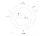
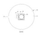
圖1A說明根據本發明之一些實施例的電子裝置1之橫截面圖。電子裝置1可包括耳機的耳塞。圖式中之電子裝置1的應用或使用僅出於說明之目的,且並不意欲限制本發明。本發明之電子裝置1可與任何可穿戴裝置組合使用,例如在一些實施例中,與傳輸音訊信號之設備組合使用。在一些實施例中,電子裝置1可與偵測裝置、電子裝置(諸如信號處理裝置)及/或其他對應外部裝置組合使用以用於進一步處理所獲取信號。FIG. 1A illustrates a cross-sectional view of an
在一些實施例中,本發明之電子裝置1可為可食用的。舉例而言,本發明之電子裝置1可安全地進食或適合於進食。舉例而言,在一些實施例中,本發明之電子裝置1可與膠囊(吞服膠囊)或其他可食用性組態組合使用。In some embodiments, the
如圖1A中所示,電子裝置1可具有可撓性元件10、感測元件(或偵測元件)11、保護層12、連接器13及主動組件14。As shown in FIG. 1A , the
可撓性元件10可具有頂側10t及與頂側10t相對之底側10m。在一些實施例中,在電子裝置1由使用者穿戴時,可撓性元件10之頂側10t比底側10m擱置得更深入於使用者之耳道中(或在其中延伸得更遠)。電子裝置1可具有在頂側10t與底側10m之間量測的高度(在圖1A中標註為「h」)。在一些實施例中,可撓性元件10之高度h可在約8毫米(mm)與約12 mm之間。舉例而言,可撓性元件10的高度h可在約9毫米與約11毫米之間。舉例而言,可撓性元件10之高度h可為約10 mm。The
可撓性元件10可具有外表面10e及與外表面10e相對之內表面10i。可撓性元件10之外表面10e可界定外徑。可撓性元件10之內表面10i可界定內徑。當電子裝置1由使用者穿戴時,可撓性元件10的外表面10e可與使用者接觸,且可撓性元件10的內表面10i可與使用者間隔開。可撓性元件10之內表面10i可界定用於收納另一件設備(諸如圖1C中所說明之一件設備15之音孔15a)之空間10r。The
外表面10e可界定電子裝置1之最大寬度或最大外徑(在圖1A中標註為「w1」)。外表面10e可界定電子裝置1之最小寬度或最小外徑(在圖1A中標註為「w2」)。在一些實施例中,可撓性元件10之寬度或外徑(包括最大外徑w1及最小外徑w2)可在約6 mm與約12 mm之間。舉例而言,可撓性元件10的寬度或外徑可在約7 mm與約11 mm之間。舉例而言,可撓性元件10的寬度或外徑可在約8 mm與約10 mm之間。The
內表面10i可界定電子裝置1之內徑(在圖1A中標註為「w3」)。在一些實施例中,寬度或內徑w3可在約1 mm與約3 mm之間,諸如約2 mm。The
在一些實施例中,可撓性元件10可包括例如橡膠、矽、海綿或其他合適材料,諸如彈性材料、軟材料或可撓性材料。在一些實施例中,可撓性元件10可包括液態聚矽氧橡膠(LSR)。In some embodiments, the
可撓性元件10可足夠軟且具有足夠可撓性,以供使用者舒適地穿戴較長時段。在一些實施例中,可撓性元件10可具有可抵抗相對更多應力、衝擊、扭轉或其他物理或結構改變之(多種)材料。舉例而言,可撓性元件10可為有彈性的,使得在受到擠壓或變形之後,其可返回至其初始狀態。在一些實施例中,當穿戴電子裝置1時,可撓性元件10可與使用者之耳道共形。在一些實施例中,載體10可靈活地調整其形狀以與使用者之耳道共形。在一些實施例中,載體10可靈活地調整其形狀以與使用者之其他身體部位共形。The
在一些實施例中,可撓性元件10可耐水、拒水或防水。在一些實施例中,可撓性元件10可耐酸、拒酸或防酸。在一些實施例中,可撓性元件10的材料可基於諸如以下各者的其他要求來選擇:聲音品質、不滲透性、皮膚友好特性(諸如,低過敏原性)等。In some embodiments, the
在一些實施例中,可撓性元件10可界定腔體10c。在一些實施例中,腔體10c可不由可撓性元件10曝露。舉例而言,腔體10c可安置於頂側10t與底側10m之間。舉例而言,腔體10c可安置於外表面10e與內表面10i之間。舉例而言,腔體10c可由可撓性元件10包圍。舉例而言,腔體10c可在可撓性元件10內,使得可撓性元件10為中空的。在一些實施例中,腔體10c可為由可撓性元件10界定之空的空間。舉例而言,腔體10c可填充有空氣。在一些實施例中,腔體10c可填充有不同於可撓性元件10的一或多種材料。In some embodiments, the
連接器13的一部分可位於腔體10c內。舉例而言,連接器13之一部分可由可撓性元件10曝露。舉例而言,連接器13可具有連接至感測元件11之一端、連接至主動組件14之另一端,且連接器13之在兩個末端之間的一部分可位於腔體10c內。A portion of the
在一些實施例中,腔體10c可充當連接器13的緩衝器。舉例而言,當可撓性元件10受擠壓或變形時,應力集中可發生於連接器13上,諸如發生於連接器13與可撓性元件10之間的界面上。腔體10c可幫助釋放或減小可撓性元件10在連接器13上的應力。舉例而言,連接器13可釋放腔體10c中之應力,從而防止其斷裂。因此,可增強電子裝置1的可靠性。In some embodiments,
感測元件11可由可撓性元件10包圍、嵌入或覆蓋。感測元件11可由保護層12包圍、嵌入或覆蓋。在一些實施例中,如圖1A中所示,感測元件11部分地嵌入於可撓性元件10中,且部分地嵌入於保護層12中。然而,在一些實施例中,感測元件11可完全嵌入於可撓性元件10中。在一些實施例中,如圖1A中所示,感測元件11自可撓性元件10之外表面10e突出。然而,在一些實施例中,感測元件11可不自可撓性元件10之外表面10e突出。感測元件11可鄰近於保護層12。感測元件11可鄰近於可撓性元件10。感測元件11可鄰近於可撓性元件10之外表面10e。The
在一些實施例中,感測元件11可為電極、熱阻器、壓力感測器、近接感測器、運動感測器、聲感測器、氣味感測器、粒子感測器、濕度感測器、光學傳輸器、光接收器、光學收發器或其組合。In some embodiments, the
在一些實施例中,感測元件11可用於偵測或收集電子裝置1外部的一或多個資訊或信號。舉例而言,感測元件11可用於偵測來自電子裝置1之周圍環境的一或多個信號。舉例而言,感測元件11可用於偵測溫度、氣壓、氣味、粒子、聲音、光、濕度或其他環境變數。舉例而言,感測元件11可用於偵測與電子裝置1之使用者相關聯的一或多個信號。舉例而言,感測元件11可用於偵測使用者之一或多個生物信號。舉例而言,由感測元件11偵測到之生物信號可由主動組件14進一步處理以判定使用者之生物參數,諸如脈衝行進時間(PTT)、腦電圖(EEG)、心電圖(ECG)、肌電圖(EMG)、眼電圖(EOG)、皮膚電反應(GSR)、汗液組成、pH值、心率可變性(HRV)或與使用者相關聯之其他生物相關資訊。In some embodiments, the
電子裝置1中之感測元件的位置、功能及數目並不意欲限制本發明。舉例而言,歸因於設計要求,電子裝置1中可能存在任何數目個感測元件。舉例而言,如圖5中所示,電子裝置5可進一步包括不同於感測元件11之感測元件50 (其將參考圖5進一步描述)。The position, function and number of sensing elements in the
在一些實施例中,保護層12可安置於可撓性元件10之外表面10e上。在一些實施例中,保護層12可覆蓋感測元件11。舉例而言,保護層12可覆蓋感測元件11之曝露部分。在一些實施例中,保護層12可經組態以保護感測元件11。In some embodiments, the
在一些實施例中,如圖1A中所示,保護層12自可撓性元件10之外表面10e突出。然而,在一些實施例中,保護層12可不自可撓性元件10之外表面10e突出。舉例而言,保護層12可與可撓性元件10之外表面10e實質上共面。In some embodiments, as shown in FIG. 1A , the
在一些實施例中,保護層12可包括如先前針對可撓性元件10列出之材料。在一些實施例中,保護層12可具有如先前針對可撓性元件10列出之特性或性質。在一些實施例中,保護層12之材料可基於感測元件11之功能而加以選擇。舉例而言,若感測元件11包括電極,則保護層12可具有相對低的阻抗,諸如超低阻抗。舉例而言,若感測元件11包括熱阻器,則保護層12可具有相對高的熱導率。舉例而言,若感測元件11包括光學感測器(諸如,光學傳輸器、光接收器或光學收發器),則保護層12可具有標準光學透明度。In some embodiments,
在一些實施例中,保護層12與可撓性元件10可具有相同材料。在一些實施例中,保護層12與可撓性元件10可具有不同材料。在一些實施例中,保護層12與可撓性元件10之間的界面可為可觀測的。在一些實施例中,保護層12與可撓性元件10之間可不存在現有界面。In some embodiments, the
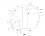
感測元件11可電連接至主動組件14以進行信號傳輸。舉例而言,感測元件11可經由連接器13電連接至主動組件14。The
在一些實施例中,連接件13可包括可撓性印刷電路(FPC)、導電線、重佈層(RDL)或其組合。感測元件11可藉由使用另一(些)替代性方法或組件連接至主動組件14。舉例而言,感測元件11可藉由使用任何橋接元件連接至主動組件14。In some embodiments, the
在一些實施例中,連接器13可安置於可撓性元件10內。舉例而言,連接器13可安置於頂側10t與底側10m之間。舉例而言,連接器13可安置於外表面10e與內表面10i之間。舉例而言,連接器13可安置於感測元件11與主動組件14之間。舉例而言,連接器13可由可撓性元件10包圍。在一些實施例中,如圖1A中所示,連接器13部分地囊封於可撓性元件10中,且連接器13的一部分在腔體10c內。舉例而言,連接器13之一部分由可撓性元件10曝露。舉例而言,連接器13之一部分曝露於空氣。In some embodiments, the
在一些實施例中,主動組件14包括系統級封裝(SiP)。在一些實施例中,主動組件14可包括資料轉換組件、處理組件、儲存組件、傳輸組件或其組合。在一些實施例中,主動組件14可包括類比至數位轉換器。In some embodiments,
在一些實施例中,主動組件14可經組態以經由連接器13自感測元件11接收信號。在一些實施例中,信號可來自由感測元件11偵測到之生物信號。在一些實施例中,主動組件14可經組態以自感測元件11接收信號。在一些實施例中,主動組件14可經組態以處理來自感測元件11之信號。在一些實施例中,信號可為類比信號,且可由主動組件14轉換為數位信號。在一些實施例中,信號可由主動組件14放大。在一些實施例中,信號可由主動組件14儲存。在一些實施例中,主動組件14可經組態以經由無線通信而自感測元件11接收信號。In some embodiments,
在一些實施例中,感測元件11與主動組件14之間的信號傳輸或信號路徑可在可撓性元件10內。舉例而言,感測元件11與主動組件14之間的信號傳輸或信號路徑可安置於頂側10t與底側10m之間。舉例而言,感測元件11與主動組件14之間的信號傳輸或信號路徑可安置於外表面10e與內表面10i之間。舉例而言,感測元件11與主動組件14之間的信號傳輸或信號路徑可由可撓性元件10包圍。舉例而言,感測元件11與主動組件14之間的信號傳輸或信號路徑可完全在可撓性元件10內。In some embodiments, the signal transmission or signal path between the
在一些實施例中,來自感測元件11之信號可在可撓性元件10內轉換為數位信號(諸如藉由主動組件14)。在一些實施例中,來自感測元件11之信號可在可撓性元件10內放大(諸如,藉由主動組件14)。在一些實施例中,來自感測元件11之信號可儲存(諸如,藉由主動組件14)於可撓性元件10內。In some embodiments, the signal from the
在一些實施例中,由於主動組件14及感測元件11併入於可撓性元件10中,因此可在可撓性元件10內處理(例如,轉換為數位信號、放大、儲存等)由感測元件11偵測到之生物信號。因此,可減少信號雜訊,且電子裝置1可提供高動態範圍信號數位化。另外,電子裝置1中之總體電路可消耗較少電力,且佔據較小區域。In some embodiments, since the
在一些實施例中,主動組件14可將經處理信號或該信號傳輸至外部裝置。舉例而言,主動組件14可鄰近於可撓性元件10之底側10m而安置,且導電元件14p (諸如主動組件14之導電接腳)可至少部分地由可撓性元件10之底側10m曝露。舉例而言,主動組件14之導電接腳可至少部分地由可撓性元件10之底側10m曝露。導電元件14p可提供電子裝置1與外部組件(例如,外部電路或電路板)之間的電連接。In some embodiments,
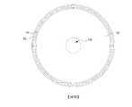
圖1B說明根據本發明之一些實施例的電子裝置之仰視圖。在一些實施例中,圖1B中之仰視圖可為圖1A中的電子裝置1之仰視圖。應注意,圖1B中僅說明可撓性元件10、保護層12、連接器13及導電元件14p,且圖1A中之電子裝置1的一些組件為了簡明起見而省略。Figure IB illustrates a bottom view of an electronic device according to some embodiments of the invention. In some embodiments, the bottom view in FIG. 1B may be the bottom view of the
如圖1B中所示,導電元件14p至少部分地由可撓性元件10曝露。虛線經說明為呈現連接器13之輪廓。自仰視圖,連接器13可位於外表面10e與內表面10i之間。舉例而言,連接器13可位於可撓性元件10 之外徑(其由外表面10e界定)與內徑(其由內表面10i界定)之間。As shown in FIG. 1B ,
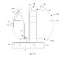
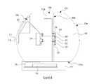
圖1C說明根據本發明之一些實施例的電子裝置之橫截面圖。在一些實施例中,圖1A中之電子裝置1可為圖1C中的電子裝置之一部分。Figure 1C illustrates a cross-sectional view of an electronic device according to some embodiments of the invention. In some embodiments, the
如圖1C中所示,在可撓性元件10中自底側10m部分地調適一件設備15。在一些實施例中,該件設備15可經組態以傳輸音訊信號。舉例而言,音孔15a可由可撓性元件10之內表面10i包圍。在一些實施例中,底側10m可經成形以收納該件設備15。As shown in FIG. 1C , a piece of
導電襯墊17可至少部分地由該件設備15曝露。導電襯墊17可與導電元件14p電連接。當自底側10m部分地在可撓性元件10中調適該件設備15時,導電襯墊17可面向底側10m。舉例而言,可根據導電元件14p配置導電襯墊17。The
導電元件14p可經由導電襯墊17及連接器18電連接至該件設備15中之電子組件16。The
在一些實施例中,電子組件16可為晶片或晶粒,包括半導體基板、一或多個積體電路裝置及其中之一或多個上覆互連結構。積體電路裝置可包括諸如電晶體之主動裝置及/或諸如電阻器、電容器、電感器之被動裝置,或其組合。在一些實施例中,電子組件16可包括處理器,諸如中央處理單元。在一些實施例中,電子組件16亦可整合至可撓性元件10中。在一些實施例中,來自感測元件11之信號可藉由主動組件14在可撓性元件10內處理(例如,轉換為數位信號、放大、儲存等),且接著傳輸至電子組件16以進行進一步信號處理。舉例而言,主動組件14可執行前端程序,且電子組件16可針對進一步應用執行後端程序,諸如資料分析、計算或資料變換。In some embodiments,
圖2A說明根據本發明之一些實施例的電子裝置2之橫截面圖。電子裝置2類似於圖1A中之電子裝置1,惟如下描述之差異除外。Figure 2A illustrates a cross-sectional view of an
如圖2A中所示,電子裝置2可具有導電元件20及21。導電元件20及21兩者皆可至少部分地由可撓性元件10之底側10m曝露。導電元件20可與導電元件21間隔開。導電元件20及21兩者皆可與主動組件14間隔開。As shown in FIG. 2A , the
電子裝置2之主動組件14可鄰近於可撓性元件10之內表面10i而安置,且可經由連接器22與導電元件20及21電連接。在一些實施例中,連接器22可包括FPC、導電線、RDL或其組合。The
電子裝置2中之導電元件的位置、功能及數目並不意欲限制本發明。舉例而言,歸因於設計要求,電子裝置2中可能存在任何數目個導電元件。The location, function and number of conductive elements in
在一些實施例中,由感測元件11偵測到之信號可經由連接器13傳輸至主動組件14以進行進一步信號處理。可接著經由連接器22將經處理信號傳輸至導電元件20及21,且最終傳輸至外部裝置。In some embodiments, the signal detected by the
圖2B說明根據本發明之一些實施例的電子裝置之仰視圖。在一些實施例中,圖2B中之仰視圖可為圖2A中的電子裝置2之仰視圖。應注意,圖2B中僅說明可撓性元件10、保護層12、連接器13以及導電元件20及21,且圖2A中之電子裝置2的一些組件為了簡明起見而省略。2B illustrates a bottom view of an electronic device according to some embodiments of the invention. In some embodiments, the bottom view in FIG. 2B may be the bottom view of the
如圖2B中所示,導電元件20及21至少部分地由可撓性元件10之底側10m曝露。虛線經說明為呈現連接器13之輪廓。自仰視圖,連接器13可與導電元件20及21重疊。As shown in FIG. 2B , the
圖2C說明根據本發明之一些實施例的電子裝置之橫截面圖。在一些實施例中,圖2A中之電子裝置2可為圖2C中的電子裝置之一部分。Figure 2C illustrates a cross-sectional view of an electronic device according to some embodiments of the invention. In some embodiments, the
導電襯墊23及24可至少部分地由該件設備15曝露。導電襯墊23可與導電元件20電連接。導電襯墊24可與導電元件21電連接。當自底側10m部分地在可撓性元件10中調適該件設備15時,導電襯墊23及24可面向底側10m。舉例而言,可根據導電元件20及21配置導電襯墊23及24。The
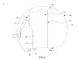
圖3A說明根據本發明之一些實施例的電子裝置3之橫截面圖。電子裝置3類似於圖2A中之電子裝置2,惟如下描述之差異除外。Figure 3A illustrates a cross-sectional view of an
導電元件30及32可至少部分地由可撓性元件10之內表面10i曝露。在一些實施例中,導電元件30及32可包括主動組件14之一或多個導電接腳。在一些實施例中,主動組件14可經由連接器(圖式中未標註)與導電元件30及32電連接。舉例而言,導電元件30及32可與主動組件14間隔開,且可經由一或多個連接器與主動組件14電連接。The
在一些實施例中,導電元件30及32可具有彎曲表面。在一些實施例中,由導電元件30及32界定之中心角可超過180°。舉例而言,導電元件30及32可環繞或包圍空間10r之中心軸線。在一些實施例中,導電元件30及32可環繞或包圍可撓性元件10之內表面10i。In some embodiments,
在一些實施例中,導電元件30可藉由絕緣元件31而與導電元件32間隔開。在一些實施例中,導電元件32可藉由絕緣元件33而與其他導電元件間隔開。在一些實施例中,絕緣元件31 (及/或絕緣元件33)可具有彎曲表面。在一些實施例中,由絕緣元件31 (及/或絕緣元件33)界定之中心角可超出180°。舉例而言,絕緣元件31 (及/或絕緣元件33)可環繞或包圍空間10r之中心軸線。在一些實施例中,絕緣元件31 (及/或絕緣元件33)可環繞或包圍可撓性元件10之內表面10i。在一些實施例中,可省略絕緣元件31及/或絕緣元件33。In some embodiments, the
在一些實施例中,由感測元件11偵測到之信號可經由連接器13傳輸至主動組件14以進行進一步信號處理。可接著將經處理信號傳輸(直接或經由另一連接器)至導電元件30及32,且最終傳輸至外部裝置。In some embodiments, the signal detected by the
圖3B說明根據本發明之一些實施例的電子裝置之橫截面圖。在一些實施例中,圖3B中之橫截面圖可為圖3A中之電子裝置3沿著線AA'之橫截面圖。應注意,圖3B中僅說明可撓性元件10、連接器13及導電元件30,且圖3B中之電子裝置3的一些組件為了簡明起見而省略。3B illustrates a cross-sectional view of an electronic device according to some embodiments of the invention. In some embodiments, the cross-sectional view in FIG. 3B may be a cross-sectional view of the
如圖3B中所示,導電元件30可至少部分地由可撓性元件10之內表面10i曝露。絕緣元件30可環繞或包圍可撓性元件10之內表面10i。絕緣元件30可為環形。As shown in FIG. 3B , the
圖3C說明根據本發明之一些實施例的電子裝置之橫截面圖。在一些實施例中,圖3A中之電子裝置3可為圖3C中的電子裝置之一部分。Figure 3C illustrates a cross-sectional view of an electronic device according to some embodiments of the invention. In some embodiments, the
導電襯墊34及35可根據導電元件30及32而配置。舉例而言,導電襯墊34可與導電元件30電連接,且導電襯墊35可與導電元件32電連接。當自底側10m部分地在可撓性元件10中調適該件設備15時,導電襯墊34及35可面向內表面10i。
導電元件30及32可經由導電襯墊34及35以及連接器18電連接至該件設備15中之電子組件16。在一些實施例中,由於導電元件30及32包圍可撓性元件10之內表面10i,因此導電襯墊34及35可與導電元件30及32對準,而無在使該件設備15旋轉時丟失資料之風險。The
圖4A說明根據本發明之一些實施例的電子裝置4之橫截面圖。圖4B說明根據本發明之一些實施例的電子裝置之橫截面圖。在一些實施例中,圖4B中之橫截面圖可為圖4A中之電子裝置4沿著線BB'之橫截面圖。圖4C說明根據本發明之一些實施例的電子裝置的一部分之透視圖。在一些實施例中,圖4C中之透視圖可為圖4A中的電子裝置4之一部分的透視圖。電子裝置4類似於圖3A中之電子裝置3,惟如下描述之差異除外。Figure 4A illustrates a cross-sectional view of an
參考圖4B,導電元件40可包圍可撓性元件10之內表面10i。導電元件40可不由可撓性元件10之內表面10i曝露。導電元件40可具有正方形或矩形形狀。導電元件40可為正方形或矩形。導電元件40可經由連接器44連接至可撓性元件10之內表面10i。可撓性元件10之一部分可安置於導電元件40與連接器44之間。導電元件40可具有實質上平坦的表面。主動組件14可具有對應於導電元件40之表面。Referring to FIG. 4B , the
在一些實施例中,導電元件40與主動組件14之間的電連接可為實質上平坦的,其提供較佳的導電及較大可靠度。In some embodiments, the electrical connection between the
連接器44可至少部分地由可撓性元件10之內表面10i曝露。連接器44可具有彎曲表面。在一些實施例中,由連接器44界定的中心角可超過180°。舉例而言,連接器44可環繞或包圍空間10r之中心軸線。在一些實施例中,連接器44可環繞或包圍可撓性元件10之內表面10i。在一些實施例中,連接器44可為環形的。The
參考圖4C,在一些實施例中,可連同導電元件40及42一起形成一或多個絕緣元件41及43。Referring to FIG. 4C , in some embodiments, one or more
圖4D說明根據本發明之一些實施例的電子裝置之橫截面圖。在一些實施例中,圖4A中之電子裝置4可為圖4D中的電子裝置之一部分。4D illustrates a cross-sectional view of an electronic device according to some embodiments of the invention. In some embodiments, the
導電襯墊34及35可根據導電元件30及32 (以及連接器44)而配置。舉例而言,導電襯墊34可經由連接器44與導電元件30電連接,且導電襯墊35可經由連接器44與導電元件32電連接。當自底側10m部分地在可撓性元件10中調適該件設備15時,導電襯墊34及35可面向內表面10i。
導電元件40及42可經由連接器44、導電襯墊34及35以及連接器18電連接至該件設備15中之電子組件16。在一些實施例中,由於連接器44包圍可撓性元件10之內表面10i,因此導電襯墊34及35可與連接器44對準,而無在使該件設備15旋轉時丟失資料之風險。在一些實施例中,可單獨地形成連接器44及導電元件(諸如導電元件40及42)。在一些實施例中,連接器44與導電元件(諸如導電元件40及42)可形成為一體。The
圖5A說明根據本發明之一些實施例的電子裝置5之橫截面圖。圖5B說明根據本發明之一些實施例的電子裝置之橫截面圖。在一些實施例中,圖5B中之橫截面圖可為圖5A中之電子裝置5沿著線CC'之橫截面圖。電子裝置5類似於圖2A中之電子裝置2,惟如下描述之差異除外。Figure 5A illustrates a cross-sectional view of an electronic device 5 according to some embodiments of the invention. Figure 5B illustrates a cross-sectional view of an electronic device according to some embodiments of the invention. In some embodiments, the cross-sectional view in FIG. 5B may be a cross-sectional view of the electronic device 5 in FIG. 5A along line CC′. Electronic device 5 is similar to
電子裝置5進一步包括感測元件50。在一些實施例中,感測元件50可具有如先前針對感測元件11所列出之功能或特性。在一些實施例中,感測元件50可為用以偵測ECG相關資訊之電極。在一些實施例中,感測元件50可安置於可撓性元件10周圍。在一些實施例中,感測元件50可環繞或包圍可撓性元件10以增大與使用者的接觸面積。舉例而言,由感測元件50界定之中心角可超過180°。舉例而言,感測元件50可環繞或包圍空間10r之中心軸線。舉例而言,自圖5B中之橫截面圖,感測元件50可為環形。在一些實施例中,與使用者之較大接觸面積可幫助收集較多信號,且改良所產生信號之準確度。The electronic device 5 further includes a
感測元件50可電連接至主動組件14以進行信號傳輸。舉例而言,感測元件50可經由連接器13電連接至主動組件14。在一些實施例中,如圖5B中所示,連接器13可環繞或包圍可撓性元件10。由連接器13界定的中心角可超過180°。The
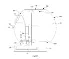
圖6說明根據本發明之一些實施例的電子裝置6之橫截面圖。電子裝置6類似於圖2A中之電子裝置2,惟如下描述之差異除外。Figure 6 illustrates a cross-sectional view of an electronic device 6 according to some embodiments of the invention. Electronic device 6 is similar to
電子裝置6進一步包括連接於主動組件14與感測元件11之間的支撐元件60。在一些實施例中,支撐元件60可為可撓性的。在一些實施例中,電子裝置6可包括例如橡膠、矽、海綿或其他合適材料,諸如彈性材料、軟材料或可撓性材料。在一些實施例中,支撐元件60可包括彈簧或線接合。The electronic device 6 further includes a supporting
在一些實施例中,支撐元件60可幫助可撓性元件10回彈及返回至其初始狀態。連接器13與支撐元件60可具有不同功能。連接器13可用以提供信號傳輸,而支撐元件60可用以改良可撓性元件10之可撓性。In some embodiments, the supporting
圖7說明根據本發明之一些實施例的電子裝置7之橫截面圖。電子裝置7類似於圖6中之電子裝置6,惟如下描述之差異除外。Figure 7 illustrates a cross-sectional view of an electronic device 7 according to some embodiments of the invention. Electronic device 7 is similar to electronic device 6 in FIG. 6 except for the differences described below.
電子裝置7之支撐元件70可係導電的。支撐元件70可電連接於主動組件14與感測元件11之間,以提供信號傳輸。因此,可省略圖6中之連接器13。在一些實施例中,支撐元件70可進一步經由連接器71與導電元件20及21電連接。The supporting
如本文所使用,除非上下文另外清楚地規定,否則單數術語「一(a/an)」及「該」可包括複數個指示物。As used herein, the singular terms "a" and "the" may include plural referents unless the context clearly dictates otherwise.
如本文所使用,術語「導電(conductive)」、「導電(electrically conductive)」及「導電率」指代傳送電流之能力。導電材料通常指示呈現對於電流流動之極小或零阻力之彼等材料。電導率之一個量度為西門子每米(S/m)。通常,導電材料為具有大於約104 S/m (諸如至少105 S/m或至少106 S/m)之導電率的一種材料。材料之電導率有時可隨溫度變化。除非另外規定,否則材料之電導率係在室溫下量測。As used herein, the terms "conductive," "electrically conductive," and "conductivity" refer to the ability to carry electrical current. Conductive materials generally refer to those materials that exhibit little or no resistance to the flow of electrical current. One measure of electrical conductivity is Siemens per meter (S/m). Typically, a conductive material is one that has a conductivity greater than about 104 S/m, such as at least 105 S/m or at least 106 S/m. The conductivity of materials can sometimes vary with temperature. Unless otherwise specified, the conductivity of the material was measured at room temperature.
如本文中所使用,術語「大致」、「實質上」、「相當大的」及「約」係用以描述及考量小的變化。當與事件或情形結合使用時,術語可指其中事件或情形明確發生之例子以及其中事件或情形極近似於發生之例子。舉例而言,當結合數值使用時,該等術語可指小於或等於彼數值之±10%的變化範圍,諸如小於或等於±5%、小於或等於±4%、小於或等於±3%、小於或等於±2%、小於或等於±1%、小於或等於±0.5%、小於或等於±0.1%或小於或等於±0.05%之變化範圍。舉例而言,若兩個數值之間的差小於或等於該等值之平均值的±10% (諸如,小於或等於±5%、小於或等於±4%、小於或等於±3%、小於或等於±2%、小於或等於±1%、小於或等於±0.5%、小於或等於±0.1%、或小於或等於±0.05%),則可認為該兩個數值「大體上」相同或相等。舉例而言,「實質上」平行可指相對於0°而言小於或等於±10°之角度變化範圍,諸如小於或等於±5°、小於或等於±4°、小於或等於±3°、小於或等於±2°、小於或等於±1°、小於或等於±0.5°、小於或等於±0.1°,或小於或等於±0.05°。舉例而言,「實質上」垂直可指相對於90°而言小於或等於±10°之角度變化範圍,諸如小於或等於±5°、小於或等於±4°、小於或等於±3°、小於或等於±2°、小於或等於±1°、小於或等於±0.5°、小於或等於±0.1°或小於或等於±0.05°的角度變化範圍。As used herein, the terms "approximately," "substantially," "substantially," and "about" are used to describe and account for small variations. When used in connection with an event or circumstance, the term can refer to instances where the event or circumstance definitely occurred as well as instances where the event or circumstance closely approximated to occur. For example, when used in conjunction with numerical values, these terms may refer to a range of variation less than or equal to ±10% of that value, such as less than or equal to ±5%, less than or equal to ±4%, less than or equal to ±3%, Less than or equal to ±2%, less than or equal to ±1%, less than or equal to ±0.5%, less than or equal to ±0.1%, or less than or equal to ±0.05%. For example, if the difference between two values is less than or equal to ±10% of the mean of those values (such as less than or equal to ±5%, less than or equal to ±4%, less than or equal to ±3%, less than or equal to ±2%, less than or equal to ±1%, less than or equal to ±0.5%, less than or equal to ±0.1%, or less than or equal to ±0.05%), the two values can be considered "substantially" the same or equal . For example, "substantially" parallel may refer to an angular range of less than or equal to ±10° relative to 0°, such as less than or equal to ±5°, less than or equal to ±4°, less than or equal to ±3°, Less than or equal to ±2°, less than or equal to ±1°, less than or equal to ±0.5°, less than or equal to ±0.1°, or less than or equal to ±0.05°. For example, "substantially" perpendicular may refer to an angular range of less than or equal to ±10° relative to 90°, such as less than or equal to ±5°, less than or equal to ±4°, less than or equal to ±3°, Angle variation range of less than or equal to ±2°, less than or equal to ±1°, less than or equal to ±0.5°, less than or equal to ±0.1°, or less than or equal to ±0.05°.
另外,有時在本文中按範圍格式提出量、比率及其他數值。應理解,此類範圍格式係為便利及簡潔起見而使用,且應靈活地理解為不僅包括明確指定為範圍限制之數值,且亦包括涵蓋於彼範圍內之所有個別數值或子範圍,如同明確指定每一數值及子範圍一般。Additionally, amounts, ratios, and other numerical values are sometimes presented herein in a range format. It should be understood that such range formats are used for convenience and brevity, and should be read flexibly to include not only the values expressly designated as limitations of the range, but also all individual values or subranges encompassed within that range, as if Explicitly specify each value and subrange in general.
儘管已參看本發明之特定實施例描述並說明本發明,但此等描述及說明並不限制本發明。熟習此項技術者應理解,在不脫離如由所附申請專利範圍界定的本發明之真實精神及範疇的情況下,可作出各種改變且可取代等效物。說明可不必按比例繪製。由於製造製程及公差,在本發明中之藝術再現與實際設備之間可能存在區別。可存在並未特定說明之本發明的其他實施例。應將本說明書及附圖視為說明性而非限制性的。可做出修改,以使特定情形、材料、物質組成、方法或程序適應於本發明之目標、精神及範疇。所有此類修改都意圖屬於在此所附的權利要求書的範圍內。儘管已參考按特定次序執行之特定操作來描述本文中所揭示之方法,但應理解,在不脫離本發明之教示的情況下,可組合、再細分,或重新定序此等操作以形成等效方法。因此,除非本文中特定指示,否則操作之次序及分組並非本發明之限制。While the invention has been described and illustrated with reference to particular embodiments of the invention, such description and illustration do not limit the invention. It will be understood by those skilled in the art that various changes may be made and equivalents may be substituted without departing from the true spirit and scope of the invention as defined by the appended claims. Illustrations may not necessarily be drawn to scale. Due to manufacturing processes and tolerances, there may be differences between the artistic reproductions in this invention and the actual device. There may be other embodiments of the invention not specifically described. The specification and drawings are to be regarded as illustrative rather than restrictive. Modifications may be made to adapt a particular situation, material, composition of matter, method or process to the objective, spirit and scope of the invention. All such modifications are intended to come within the scope of the claims appended hereto. Although the methods disclosed herein have been described with reference to particular operations performed in a particular order, it should be understood that these operations may be combined, subdivided, or reordered to form other operations without departing from the teachings of the invention. effective method. Thus, unless specifically indicated herein, the order and grouping of operations is not a limitation of the invention.
1:電子裝置 2:電子裝置 3:電子裝置 4:電子裝置 5:電子裝置 6:電子裝置 7:電子裝置 10:可撓性元件/載體 10c:腔體 10e:外表面 10i:內表面 10m:底側 10r:空間 10t:頂側 11:感測元件 12:保護層 13:連接器 14:主動組件 14p:導電元件 15:設備 15a:音孔 16:電子組件 17:導電襯墊 18:連接器 20:導電元件 21:導電元件 22:連接器 23:導電襯墊 24:導電襯墊 30:導電元件 31:絕緣元件 32:導電元件 33:絕緣元件 34:導電襯墊 35:導電襯墊 40:導電元件 41:絕緣元件 42:導電元件 43:絕緣元件 44:連接器 50:感測元件 60:支撐元件 70:支撐元件 71:連接器 h:高度 w1:最大外徑 w2:最小外徑 w3:內徑1: Electronic device 2: Electronic device 3: Electronic device 4: Electronic device 5: Electronic device 6: Electronic device 7: Electronic device 10: Flexible elements/
當結合附圖閱讀時,自以下實施方式最佳地理解本發明之一些實施例的態樣。應注意,各種結構可能未按比例繪製,且各種結構之尺寸可出於論述清晰起見任意增大或減小。Aspects of some embodiments of this invention are best understood from the following description when read with the accompanying drawings. It should be noted that the various structures may not be drawn to scale and that the dimensions of the various structures may be arbitrarily increased or decreased for clarity of discussion.
圖1A說明根據本發明之一些實施例的電子裝置之橫截面圖。Figure 1A illustrates a cross-sectional view of an electronic device according to some embodiments of the invention.
圖1B說明根據本發明之一些實施例的電子裝置之仰視圖。Figure IB illustrates a bottom view of an electronic device according to some embodiments of the invention.
圖1C說明根據本發明之一些實施例的電子裝置之橫截面圖。Figure 1C illustrates a cross-sectional view of an electronic device according to some embodiments of the invention.
圖2A說明根據本發明之一些實施例的電子裝置之橫截面圖。Figure 2A illustrates a cross-sectional view of an electronic device according to some embodiments of the invention.
圖2B說明根據本發明之一些實施例的電子裝置之仰視圖。2B illustrates a bottom view of an electronic device according to some embodiments of the invention.
圖2C說明根據本發明之一些實施例的電子裝置之橫截面圖。Figure 2C illustrates a cross-sectional view of an electronic device according to some embodiments of the invention.
圖3A說明根據本發明之一些實施例的電子裝置之橫截面圖。Figure 3A illustrates a cross-sectional view of an electronic device according to some embodiments of the invention.
圖3B說明根據本發明之一些實施例的電子裝置之橫截面圖。3B illustrates a cross-sectional view of an electronic device according to some embodiments of the invention.
圖3C說明根據本發明之一些實施例的電子裝置之橫截面圖。Figure 3C illustrates a cross-sectional view of an electronic device according to some embodiments of the invention.
圖4A說明根據本發明之一些實施例的電子裝置之橫截面圖。Figure 4A illustrates a cross-sectional view of an electronic device according to some embodiments of the invention.
圖4B說明根據本發明之一些實施例的電子裝置之橫截面圖。4B illustrates a cross-sectional view of an electronic device according to some embodiments of the invention.
圖4C說明根據本發明之一些實施例的電子裝置的一部分之透視圖。4C illustrates a perspective view of a portion of an electronic device according to some embodiments of the invention.
圖4D說明根據本發明之一些實施例的電子裝置之橫截面圖。4D illustrates a cross-sectional view of an electronic device according to some embodiments of the invention.
圖5A說明根據本發明之一些實施例的電子裝置之橫截面圖。Figure 5A illustrates a cross-sectional view of an electronic device according to some embodiments of the invention.
圖5B說明根據本發明之一些實施例的電子裝置之橫截面圖。Figure 5B illustrates a cross-sectional view of an electronic device according to some embodiments of the invention.
圖6說明根據本發明之一些實施例的電子裝置之橫截面圖。6 illustrates a cross-sectional view of an electronic device according to some embodiments of the invention.
圖7說明根據本發明之一些實施例的電子裝置之橫截面圖。7 illustrates a cross-sectional view of an electronic device according to some embodiments of the invention.
1:電子裝置1: Electronic device
10:可撓性元件/載體10: Flexible elements/carriers
10c:腔體10c: cavity
10e:外表面10e: Outer surface
10i:內表面10i: inner surface
10m:底側10m: bottom side
10r:空間10r: space
10t:頂側10t: top side
11:感測元件11: Sensing element
12:保護層12: Protective layer
13:連接器13: Connector
14:主動組件14: Active components
14p:導電元件14p: conductive element
h:高度h: height
w1:最大外徑w1: maximum outer diameter
w2:最小外徑w2: Minimum outer diameter
w3:內徑w3: inner diameter
Claims (20)
Translated fromChineseApplications Claiming Priority (2)
| Application Number | Priority Date | Filing Date | Title |
|---|---|---|---|
| US17/244,876US12245872B2 (en) | 2021-04-29 | 2021-04-29 | Electronic device |
| US17/244,876 | 2021-04-29 |
Publications (1)
| Publication Number | Publication Date |
|---|---|
| TW202241344Atrue TW202241344A (en) | 2022-11-01 |
Family
ID=83760045
Family Applications (1)
| Application Number | Title | Priority Date | Filing Date |
|---|---|---|---|
| TW111115514ATW202241344A (en) | 2021-04-29 | 2022-04-22 | Electronic device and method of manufacturing the same |
Country Status (3)
| Country | Link |
|---|---|
| US (2) | US12245872B2 (en) |
| CN (1) | CN115251835A (en) |
| TW (1) | TW202241344A (en) |
Families Citing this family (3)
| Publication number | Priority date | Publication date | Assignee | Title |
|---|---|---|---|---|
| US20240112975A1 (en)* | 2022-10-03 | 2024-04-04 | Amkor Technology Singapore Holding Pte. Ltd. | Electronic devices and methods of manufacturing electronic devices |
| US20240197176A1 (en)* | 2022-12-16 | 2024-06-20 | Advanced Semiconductor Engineering, Inc. | Sensing device |
| US20250080895A1 (en)* | 2023-08-31 | 2025-03-06 | Advanced Semiconductor Engineering, Inc. | Electronic device |
Family Cites Families (8)
| Publication number | Priority date | Publication date | Assignee | Title |
|---|---|---|---|---|
| DE102007046295A1 (en)* | 2006-11-15 | 2009-04-16 | Buschmann, Johannes, Prof. Dr. med. | Methods and apparatus for the continuous and mobile measurement of various vital parameters in the external auditory canal, in particular measurement of the ECG, the body (core) temperature, tissue-optical parameters |
| US20190246982A1 (en)* | 2015-08-05 | 2019-08-15 | Emotiv Inc. | Method and system for collecting and processing bioelectrical signals |
| US10257602B2 (en)* | 2017-08-07 | 2019-04-09 | Bose Corporation | Earbud insertion sensing method with infrared technology |
| CN111936044B (en)* | 2018-02-09 | 2024-03-08 | 阿尔伯特-路德维希-弗莱堡大学 | Sensor array, method for operating a sensor array and computer program for executing a method for operating a sensor array |
| EP3761932A4 (en)* | 2018-03-09 | 2022-01-05 | Earsoft, LLC | Eartips and earphone devices, and systems and methods therefore |
| US11647954B2 (en)* | 2019-11-08 | 2023-05-16 | International Business Machines Corporation | Ear device for heat stroke detection |
| US11523208B2 (en)* | 2020-03-18 | 2022-12-06 | Advanced Semiconductor Engineering, Inc. | Eartip and a wearable device including an eartip |
| JP2022059147A (en)* | 2020-10-01 | 2022-04-13 | 株式会社Agama-X | Biometric information measurement system |
- 2021
- 2021-04-29USUS17/244,876patent/US12245872B2/enactiveActive
- 2022
- 2022-04-22TWTW111115514Apatent/TW202241344A/enunknown
- 2022-04-29CNCN202210472644.5Apatent/CN115251835A/enactivePending
- 2025
- 2025-03-11USUS19/077,025patent/US20250204854A1/enactivePending
Also Published As
| Publication number | Publication date |
|---|---|
| US20220346715A1 (en) | 2022-11-03 |
| US12245872B2 (en) | 2025-03-11 |
| CN115251835A (en) | 2022-11-01 |
| US20250204854A1 (en) | 2025-06-26 |
Similar Documents
| Publication | Publication Date | Title |
|---|---|---|
| TW202241344A (en) | Electronic device and method of manufacturing the same | |
| CN104665806B (en) | Electrode, biosignal detection device and method for measuring biosignal | |
| US8287451B2 (en) | Flexible biomonitor with EMI shielding and module expansion | |
| KR101747858B1 (en) | Electrode for living body and device for measuring living body signal | |
| US20160128597A1 (en) | Thin planar biological sensor | |
| US12171561B2 (en) | Cuff with integrated signal recorder for long-term measurements of biosignals from a living body | |
| US8937481B2 (en) | Capacitive sensing apparatus | |
| JP2005521458A (en) | Monitoring system with electrodes with protrusions | |
| JP7705710B2 (en) | Ear tip and wearable device including same | |
| US20180028071A1 (en) | Wearable patch for measuring temperature and electrical signals | |
| US6687524B1 (en) | Disposable neonatal electrode for use in a high humidity environment | |
| US20250133322A1 (en) | Wearable component, ear tip, and method of manufacturing a wearable component | |
| US20250134456A1 (en) | Wearable device | |
| CN207236785U (en) | Disposable biological electricity electrode | |
| US20230148932A1 (en) | Wearable Sensor | |
| CN210158594U (en) | Earplugs and Bioelectric Signal Detection Device | |
| US12396681B2 (en) | Wearable device | |
| CN214017583U (en) | A wireless BAEP signal acquisition device | |
| CN222917532U (en) | An in-ear multimodal sensing system for continuous monitoring of brain activity and sweat lactate | |
| JPWO2022251636A5 (en) | ||
| KR101357671B1 (en) | Structure and fabrication method of dry bio-electrode with super hydrophobic surface for measurement of living body signal | |
| KR100731676B1 (en) | Electrode Patches for Measuring Cardiac Electrical Activity in Mobile Environments |