TW202223154A - Methods and apparatus for low resistivity and stress tungsten gap fill - Google Patents
Methods and apparatus for low resistivity and stress tungsten gap fillDownload PDFInfo
- Publication number
- TW202223154A TW202223154ATW110137930ATW110137930ATW202223154ATW 202223154 ATW202223154 ATW 202223154ATW 110137930 ATW110137930 ATW 110137930ATW 110137930 ATW110137930 ATW 110137930ATW 202223154 ATW202223154 ATW 202223154A
- Authority
- TW
- Taiwan
- Prior art keywords
- tungsten
- degrees celsius
- fill
- temperature
- bulk
- Prior art date
Links
- 238000000034methodMethods0.000titleclaimsabstractdescription138
- 229910052721tungstenInorganic materials0.000titleclaimsabstractdescription136
- 239000010937tungstenSubstances0.000titleclaimsabstractdescription136
- WFKWXMTUELFFGS-UHFFFAOYSA-NtungstenChemical compound[W]WFKWXMTUELFFGS-UHFFFAOYSA-N0.000titleclaimsabstractdescription127
- 230000008569processEffects0.000claimsabstractdescription83
- 238000005229chemical vapour depositionMethods0.000claimsabstractdescription47
- 238000005240physical vapour depositionMethods0.000claimsabstractdescription39
- XKRFYHLGVUSROY-UHFFFAOYSA-NArgonChemical compound[Ar]XKRFYHLGVUSROY-UHFFFAOYSA-N0.000claimsabstractdescription28
- 238000000151depositionMethods0.000claimsabstractdescription24
- 229910052786argonInorganic materials0.000claimsabstractdescription14
- 229910052743kryptonInorganic materials0.000claimsabstractdescription11
- DNNSSWSSYDEUBZ-UHFFFAOYSA-Nkrypton atomChemical compound[Kr]DNNSSWSSYDEUBZ-UHFFFAOYSA-N0.000claimsabstractdescription11
- 239000007789gasSubstances0.000claimsabstractdescription10
- ZOXJGFHDIHLPTG-UHFFFAOYSA-NBoronChemical compound[B]ZOXJGFHDIHLPTG-UHFFFAOYSA-N0.000claimsabstractdescription8
- 229910052796boronInorganic materials0.000claimsabstractdescription8
- 238000000231atomic layer depositionMethods0.000claimsdescription20
- 230000006911nucleationEffects0.000claimsdescription19
- 238000010899nucleationMethods0.000claimsdescription19
- 238000011282treatmentMethods0.000claimsdescription15
- 238000005121nitridingMethods0.000claimsdescription11
- IJGRMHOSHXDMSA-UHFFFAOYSA-NAtomic nitrogenChemical compoundN#NIJGRMHOSHXDMSA-UHFFFAOYSA-N0.000claimsdescription8
- 229910052757nitrogenInorganic materials0.000claimsdescription4
- 230000008021depositionEffects0.000description15
- 239000000758substrateSubstances0.000description14
- 238000000137annealingMethods0.000description11
- -1tungsten nitrideChemical class0.000description9
- 239000001257hydrogenSubstances0.000description7
- 229910052739hydrogenInorganic materials0.000description7
- UFHFLCQGNIYNRP-UHFFFAOYSA-NHydrogenChemical compound[H][H]UFHFLCQGNIYNRP-UHFFFAOYSA-N0.000description5
- 230000015572biosynthetic processEffects0.000description5
- 239000002243precursorSubstances0.000description5
- 229910052751metalInorganic materials0.000description4
- 239000002184metalSubstances0.000description4
- 229910052756noble gasInorganic materials0.000description4
- 150000002835noble gasesChemical class0.000description4
- 238000005516engineering processMethods0.000description3
- 208000012766Growth delayDiseases0.000description2
- NRTOMJZYCJJWKI-UHFFFAOYSA-NTitanium nitrideChemical compound[Ti]#NNRTOMJZYCJJWKI-UHFFFAOYSA-N0.000description2
- 230000006399behaviorEffects0.000description2
- 150000002431hydrogenChemical class0.000description2
- 239000004065semiconductorSubstances0.000description2
- 238000007669thermal treatmentMethods0.000description2
- NXHILIPIEUBEPD-UHFFFAOYSA-Htungsten hexafluorideChemical compoundF[W](F)(F)(F)(F)FNXHILIPIEUBEPD-UHFFFAOYSA-H0.000description2
- BLRPTPMANUNPDV-UHFFFAOYSA-NSilaneChemical compound[SiH4]BLRPTPMANUNPDV-UHFFFAOYSA-N0.000description1
- ATJFFYVFTNAWJD-UHFFFAOYSA-NTinChemical compound[Sn]ATJFFYVFTNAWJD-UHFFFAOYSA-N0.000description1
- 150000001638boronChemical class0.000description1
- 239000004020conductorSubstances0.000description1
- 238000005137deposition processMethods0.000description1
- ZOCHARZZJNPSEU-UHFFFAOYSA-NdiboronChemical compoundB#BZOCHARZZJNPSEU-UHFFFAOYSA-N0.000description1
- 238000011534incubationMethods0.000description1
- 230000010354integrationEffects0.000description1
- 230000007246mechanismEffects0.000description1
- 230000009467reductionEffects0.000description1
- 230000004044responseEffects0.000description1
- 229910000077silaneInorganic materials0.000description1
Images


Classifications
- H—ELECTRICITY
- H01—ELECTRIC ELEMENTS
- H01L—SEMICONDUCTOR DEVICES NOT COVERED BY CLASS H10
- H01L21/00—Processes or apparatus adapted for the manufacture or treatment of semiconductor or solid state devices or of parts thereof
- H01L21/70—Manufacture or treatment of devices consisting of a plurality of solid state components formed in or on a common substrate or of parts thereof; Manufacture of integrated circuit devices or of parts thereof
- H01L21/71—Manufacture of specific parts of devices defined in group H01L21/70
- H01L21/768—Applying interconnections to be used for carrying current between separate components within a device comprising conductors and dielectrics
- H01L21/76838—Applying interconnections to be used for carrying current between separate components within a device comprising conductors and dielectrics characterised by the formation and the after-treatment of the conductors
- H01L21/76841—Barrier, adhesion or liner layers
- H01L21/76871—Layers specifically deposited to enhance or enable the nucleation of further layers, i.e. seed layers
- H01L21/76876—Layers specifically deposited to enhance or enable the nucleation of further layers, i.e. seed layers for deposition from the gas phase, e.g. CVD
- H—ELECTRICITY
- H01—ELECTRIC ELEMENTS
- H01L—SEMICONDUCTOR DEVICES NOT COVERED BY CLASS H10
- H01L21/00—Processes or apparatus adapted for the manufacture or treatment of semiconductor or solid state devices or of parts thereof
- H01L21/70—Manufacture or treatment of devices consisting of a plurality of solid state components formed in or on a common substrate or of parts thereof; Manufacture of integrated circuit devices or of parts thereof
- H01L21/71—Manufacture of specific parts of devices defined in group H01L21/70
- H01L21/768—Applying interconnections to be used for carrying current between separate components within a device comprising conductors and dielectrics
- H01L21/76838—Applying interconnections to be used for carrying current between separate components within a device comprising conductors and dielectrics characterised by the formation and the after-treatment of the conductors
- H01L21/76877—Filling of holes, grooves or trenches, e.g. vias, with conductive material
- H01L21/76879—Filling of holes, grooves or trenches, e.g. vias, with conductive material by selective deposition of conductive material in the vias, e.g. selective C.V.D. on semiconductor material, plating
- C—CHEMISTRY; METALLURGY
- C23—COATING METALLIC MATERIAL; COATING MATERIAL WITH METALLIC MATERIAL; CHEMICAL SURFACE TREATMENT; DIFFUSION TREATMENT OF METALLIC MATERIAL; COATING BY VACUUM EVAPORATION, BY SPUTTERING, BY ION IMPLANTATION OR BY CHEMICAL VAPOUR DEPOSITION, IN GENERAL; INHIBITING CORROSION OF METALLIC MATERIAL OR INCRUSTATION IN GENERAL
- C23C—COATING METALLIC MATERIAL; COATING MATERIAL WITH METALLIC MATERIAL; SURFACE TREATMENT OF METALLIC MATERIAL BY DIFFUSION INTO THE SURFACE, BY CHEMICAL CONVERSION OR SUBSTITUTION; COATING BY VACUUM EVAPORATION, BY SPUTTERING, BY ION IMPLANTATION OR BY CHEMICAL VAPOUR DEPOSITION, IN GENERAL
- C23C16/00—Chemical coating by decomposition of gaseous compounds, without leaving reaction products of surface material in the coating, i.e. chemical vapour deposition [CVD] processes
- C23C16/02—Pretreatment of the material to be coated
- C23C16/0272—Deposition of sub-layers, e.g. to promote the adhesion of the main coating
- C23C16/0281—Deposition of sub-layers, e.g. to promote the adhesion of the main coating of metallic sub-layers
- C—CHEMISTRY; METALLURGY
- C23—COATING METALLIC MATERIAL; COATING MATERIAL WITH METALLIC MATERIAL; CHEMICAL SURFACE TREATMENT; DIFFUSION TREATMENT OF METALLIC MATERIAL; COATING BY VACUUM EVAPORATION, BY SPUTTERING, BY ION IMPLANTATION OR BY CHEMICAL VAPOUR DEPOSITION, IN GENERAL; INHIBITING CORROSION OF METALLIC MATERIAL OR INCRUSTATION IN GENERAL
- C23C—COATING METALLIC MATERIAL; COATING MATERIAL WITH METALLIC MATERIAL; SURFACE TREATMENT OF METALLIC MATERIAL BY DIFFUSION INTO THE SURFACE, BY CHEMICAL CONVERSION OR SUBSTITUTION; COATING BY VACUUM EVAPORATION, BY SPUTTERING, BY ION IMPLANTATION OR BY CHEMICAL VAPOUR DEPOSITION, IN GENERAL
- C23C16/00—Chemical coating by decomposition of gaseous compounds, without leaving reaction products of surface material in the coating, i.e. chemical vapour deposition [CVD] processes
- C23C16/04—Coating on selected surface areas, e.g. using masks
- C23C16/045—Coating cavities or hollow spaces, e.g. interior of tubes; Infiltration of porous substrates
- C—CHEMISTRY; METALLURGY
- C23—COATING METALLIC MATERIAL; COATING MATERIAL WITH METALLIC MATERIAL; CHEMICAL SURFACE TREATMENT; DIFFUSION TREATMENT OF METALLIC MATERIAL; COATING BY VACUUM EVAPORATION, BY SPUTTERING, BY ION IMPLANTATION OR BY CHEMICAL VAPOUR DEPOSITION, IN GENERAL; INHIBITING CORROSION OF METALLIC MATERIAL OR INCRUSTATION IN GENERAL
- C23C—COATING METALLIC MATERIAL; COATING MATERIAL WITH METALLIC MATERIAL; SURFACE TREATMENT OF METALLIC MATERIAL BY DIFFUSION INTO THE SURFACE, BY CHEMICAL CONVERSION OR SUBSTITUTION; COATING BY VACUUM EVAPORATION, BY SPUTTERING, BY ION IMPLANTATION OR BY CHEMICAL VAPOUR DEPOSITION, IN GENERAL
- C23C16/00—Chemical coating by decomposition of gaseous compounds, without leaving reaction products of surface material in the coating, i.e. chemical vapour deposition [CVD] processes
- C23C16/06—Chemical coating by decomposition of gaseous compounds, without leaving reaction products of surface material in the coating, i.e. chemical vapour deposition [CVD] processes characterised by the deposition of metallic material
- C23C16/08—Chemical coating by decomposition of gaseous compounds, without leaving reaction products of surface material in the coating, i.e. chemical vapour deposition [CVD] processes characterised by the deposition of metallic material from metal halides
- C23C16/14—Deposition of only one other metal element
- C—CHEMISTRY; METALLURGY
- C23—COATING METALLIC MATERIAL; COATING MATERIAL WITH METALLIC MATERIAL; CHEMICAL SURFACE TREATMENT; DIFFUSION TREATMENT OF METALLIC MATERIAL; COATING BY VACUUM EVAPORATION, BY SPUTTERING, BY ION IMPLANTATION OR BY CHEMICAL VAPOUR DEPOSITION, IN GENERAL; INHIBITING CORROSION OF METALLIC MATERIAL OR INCRUSTATION IN GENERAL
- C23C—COATING METALLIC MATERIAL; COATING MATERIAL WITH METALLIC MATERIAL; SURFACE TREATMENT OF METALLIC MATERIAL BY DIFFUSION INTO THE SURFACE, BY CHEMICAL CONVERSION OR SUBSTITUTION; COATING BY VACUUM EVAPORATION, BY SPUTTERING, BY ION IMPLANTATION OR BY CHEMICAL VAPOUR DEPOSITION, IN GENERAL
- C23C16/00—Chemical coating by decomposition of gaseous compounds, without leaving reaction products of surface material in the coating, i.e. chemical vapour deposition [CVD] processes
- C23C16/44—Chemical coating by decomposition of gaseous compounds, without leaving reaction products of surface material in the coating, i.e. chemical vapour deposition [CVD] processes characterised by the method of coating
- C23C16/455—Chemical coating by decomposition of gaseous compounds, without leaving reaction products of surface material in the coating, i.e. chemical vapour deposition [CVD] processes characterised by the method of coating characterised by the method used for introducing gases into reaction chamber or for modifying gas flows in reaction chamber
- C23C16/45523—Pulsed gas flow or change of composition over time
- C23C16/45525—Atomic layer deposition [ALD]
- C—CHEMISTRY; METALLURGY
- C23—COATING METALLIC MATERIAL; COATING MATERIAL WITH METALLIC MATERIAL; CHEMICAL SURFACE TREATMENT; DIFFUSION TREATMENT OF METALLIC MATERIAL; COATING BY VACUUM EVAPORATION, BY SPUTTERING, BY ION IMPLANTATION OR BY CHEMICAL VAPOUR DEPOSITION, IN GENERAL; INHIBITING CORROSION OF METALLIC MATERIAL OR INCRUSTATION IN GENERAL
- C23C—COATING METALLIC MATERIAL; COATING MATERIAL WITH METALLIC MATERIAL; SURFACE TREATMENT OF METALLIC MATERIAL BY DIFFUSION INTO THE SURFACE, BY CHEMICAL CONVERSION OR SUBSTITUTION; COATING BY VACUUM EVAPORATION, BY SPUTTERING, BY ION IMPLANTATION OR BY CHEMICAL VAPOUR DEPOSITION, IN GENERAL
- C23C16/00—Chemical coating by decomposition of gaseous compounds, without leaving reaction products of surface material in the coating, i.e. chemical vapour deposition [CVD] processes
- C23C16/56—After-treatment
- H—ELECTRICITY
- H01—ELECTRIC ELEMENTS
- H01L—SEMICONDUCTOR DEVICES NOT COVERED BY CLASS H10
- H01L21/00—Processes or apparatus adapted for the manufacture or treatment of semiconductor or solid state devices or of parts thereof
- H01L21/02—Manufacture or treatment of semiconductor devices or of parts thereof
- H01L21/02104—Forming layers
- H01L21/02365—Forming inorganic semiconducting materials on a substrate
- H01L21/02612—Formation types
- H01L21/02617—Deposition types
- H01L21/0262—Reduction or decomposition of gaseous compounds, e.g. CVD
- H—ELECTRICITY
- H01—ELECTRIC ELEMENTS
- H01L—SEMICONDUCTOR DEVICES NOT COVERED BY CLASS H10
- H01L21/00—Processes or apparatus adapted for the manufacture or treatment of semiconductor or solid state devices or of parts thereof
- H01L21/02—Manufacture or treatment of semiconductor devices or of parts thereof
- H01L21/04—Manufacture or treatment of semiconductor devices or of parts thereof the devices having potential barriers, e.g. a PN junction, depletion layer or carrier concentration layer
- H01L21/18—Manufacture or treatment of semiconductor devices or of parts thereof the devices having potential barriers, e.g. a PN junction, depletion layer or carrier concentration layer the devices having semiconductor bodies comprising elements of Group IV of the Periodic Table or AIIIBV compounds with or without impurities, e.g. doping materials
- H01L21/28—Manufacture of electrodes on semiconductor bodies using processes or apparatus not provided for in groups H01L21/20 - H01L21/268
- H01L21/283—Deposition of conductive or insulating materials for electrodes conducting electric current
- H01L21/285—Deposition of conductive or insulating materials for electrodes conducting electric current from a gas or vapour, e.g. condensation
- H01L21/28506—Deposition of conductive or insulating materials for electrodes conducting electric current from a gas or vapour, e.g. condensation of conductive layers
- H01L21/28512—Deposition of conductive or insulating materials for electrodes conducting electric current from a gas or vapour, e.g. condensation of conductive layers on semiconductor bodies comprising elements of Group IV of the Periodic Table
- H01L21/28556—Deposition of conductive or insulating materials for electrodes conducting electric current from a gas or vapour, e.g. condensation of conductive layers on semiconductor bodies comprising elements of Group IV of the Periodic Table by chemical means, e.g. CVD, LPCVD, PECVD, laser CVD
- H—ELECTRICITY
- H01—ELECTRIC ELEMENTS
- H01L—SEMICONDUCTOR DEVICES NOT COVERED BY CLASS H10
- H01L21/00—Processes or apparatus adapted for the manufacture or treatment of semiconductor or solid state devices or of parts thereof
- H01L21/70—Manufacture or treatment of devices consisting of a plurality of solid state components formed in or on a common substrate or of parts thereof; Manufacture of integrated circuit devices or of parts thereof
- H01L21/71—Manufacture of specific parts of devices defined in group H01L21/70
- H01L21/768—Applying interconnections to be used for carrying current between separate components within a device comprising conductors and dielectrics
- H01L21/76838—Applying interconnections to be used for carrying current between separate components within a device comprising conductors and dielectrics characterised by the formation and the after-treatment of the conductors
- H01L21/76841—Barrier, adhesion or liner layers
- H01L21/76843—Barrier, adhesion or liner layers formed in openings in a dielectric
- H—ELECTRICITY
- H01—ELECTRIC ELEMENTS
- H01L—SEMICONDUCTOR DEVICES NOT COVERED BY CLASS H10
- H01L21/00—Processes or apparatus adapted for the manufacture or treatment of semiconductor or solid state devices or of parts thereof
- H01L21/70—Manufacture or treatment of devices consisting of a plurality of solid state components formed in or on a common substrate or of parts thereof; Manufacture of integrated circuit devices or of parts thereof
- H01L21/71—Manufacture of specific parts of devices defined in group H01L21/70
- H01L21/768—Applying interconnections to be used for carrying current between separate components within a device comprising conductors and dielectrics
- H01L21/76838—Applying interconnections to be used for carrying current between separate components within a device comprising conductors and dielectrics characterised by the formation and the after-treatment of the conductors
- H01L21/76841—Barrier, adhesion or liner layers
- H01L21/76853—Barrier, adhesion or liner layers characterized by particular after-treatment steps
- H01L21/76855—After-treatment introducing at least one additional element into the layer
- H01L21/76856—After-treatment introducing at least one additional element into the layer by treatment in plasmas or gaseous environments, e.g. nitriding a refractory metal liner
- H—ELECTRICITY
- H01—ELECTRIC ELEMENTS
- H01L—SEMICONDUCTOR DEVICES NOT COVERED BY CLASS H10
- H01L21/00—Processes or apparatus adapted for the manufacture or treatment of semiconductor or solid state devices or of parts thereof
- H01L21/70—Manufacture or treatment of devices consisting of a plurality of solid state components formed in or on a common substrate or of parts thereof; Manufacture of integrated circuit devices or of parts thereof
- H01L21/71—Manufacture of specific parts of devices defined in group H01L21/70
- H01L21/768—Applying interconnections to be used for carrying current between separate components within a device comprising conductors and dielectrics
- H01L21/76838—Applying interconnections to be used for carrying current between separate components within a device comprising conductors and dielectrics characterised by the formation and the after-treatment of the conductors
- H01L21/76877—Filling of holes, grooves or trenches, e.g. vias, with conductive material
- H01L21/76883—Post-treatment or after-treatment of the conductive material
- H—ELECTRICITY
- H01—ELECTRIC ELEMENTS
- H01L—SEMICONDUCTOR DEVICES NOT COVERED BY CLASS H10
- H01L23/00—Details of semiconductor or other solid state devices
- H01L23/52—Arrangements for conducting electric current within the device in operation from one component to another, i.e. interconnections, e.g. wires, lead frames
- H01L23/522—Arrangements for conducting electric current within the device in operation from one component to another, i.e. interconnections, e.g. wires, lead frames including external interconnections consisting of a multilayer structure of conductive and insulating layers inseparably formed on the semiconductor body
- H01L23/532—Arrangements for conducting electric current within the device in operation from one component to another, i.e. interconnections, e.g. wires, lead frames including external interconnections consisting of a multilayer structure of conductive and insulating layers inseparably formed on the semiconductor body characterised by the materials
- H01L23/53204—Conductive materials
- H01L23/53209—Conductive materials based on metals, e.g. alloys, metal silicides
- H01L23/53257—Conductive materials based on metals, e.g. alloys, metal silicides the principal metal being a refractory metal
- H01L23/53266—Additional layers associated with refractory-metal layers, e.g. adhesion, barrier, cladding layers
Landscapes
- Chemical & Material Sciences (AREA)
- Engineering & Computer Science (AREA)
- Physics & Mathematics (AREA)
- Condensed Matter Physics & Semiconductors (AREA)
- General Physics & Mathematics (AREA)
- Manufacturing & Machinery (AREA)
- Computer Hardware Design (AREA)
- Microelectronics & Electronic Packaging (AREA)
- Power Engineering (AREA)
- Chemical Kinetics & Catalysis (AREA)
- General Chemical & Material Sciences (AREA)
- Materials Engineering (AREA)
- Mechanical Engineering (AREA)
- Metallurgy (AREA)
- Organic Chemistry (AREA)
- Plasma & Fusion (AREA)
- Electrodes Of Semiconductors (AREA)
- Chemical Vapour Deposition (AREA)
- Internal Circuitry In Semiconductor Integrated Circuit Devices (AREA)
- Physical Vapour Deposition (AREA)
Abstract
Description
Translated fromChinese本原理的實施例大致關於半導體基板的處理。Embodiments of the present principles generally relate to the processing of semiconductor substrates.
鎢在半導體工業中使用作為具有最小電氣遷移的低電阻導體。鎢可用以填充孔洞作為用於電晶體的接觸及積體電路的層之間的貫孔的形成。歸因於鎢的穩定性及低電阻率,鎢亦可在邏輯及記憶體元件中用於內部連接。隨著技術發展,建立對甚至更低電阻率及更低應力金屬填充方案的需求。目前技術使用鎢的化學氣相沉積而需要使用氮化鈦襯墊及鎢原子層沉積成核隨後為鎢的塊體填充。然而,目前的方式並非技術的極限且無法提供具有更低電阻率及合理間隙填充的低應力兩者的金屬填充方案。Tungsten is used in the semiconductor industry as a low resistance conductor with minimal electromigration. Tungsten can be used to fill holes as contacts for transistors and formation of vias between layers of integrated circuits. Due to tungsten's stability and low resistivity, tungsten can also be used for interconnects in logic and memory devices. As technology develops, there is a need for even lower resistivity and lower stress metal fill solutions. Current techniques use chemical vapor deposition of tungsten and require the use of titanium nitride liners and atomic layer deposition of tungsten for nucleation followed by bulk filling of tungsten. However, the current approach is not the limit of the technology and cannot provide a metal filling solution with both lower resistivity and low stress with reasonable gap filling.
因此,發明人已提供強化的處理,而生產具有低應力且甚至比目前技術更低電阻率的鎢填充。Accordingly, the inventors have provided enhanced processing to produce tungsten fills with low stress and even lower resistivity than current technology.
此處提供用於減少鎢的內部應力同時降低鎢的電阻率之方法及裝置。Provided herein are methods and apparatus for reducing the internal stress of tungsten while reducing the resistivity of tungsten.
在某些實施例中,一種用於在一結構上形成鎢間隙填充之方法,可包含使用一物理氣相沉積(PVD)處理在該結構中沉積一鎢襯墊;使用一原子層沉積(ALD)處理沉積一成核層;以一氮化處理處置該結構:及使用一化學氣相沉積(CVD)處理沉積塊體填充鎢至該結構中,配置成形成一接縫抑制的鎢填充。In certain embodiments, a method for forming a tungsten gapfill on a structure may include depositing a tungsten liner in the structure using a physical vapor deposition (PVD) process; using an atomic layer deposition (ALD) process ) process to deposit a nucleation layer; dispose of the structure with a nitridation process; and use a chemical vapor deposition (CVD) process to deposit bulk fill tungsten into the structure, configured to form a seam-inhibited tungsten fill.
在某些實施例中,方法可進一步包括其中該成核層為大約10埃至大約60埃的厚度;其中該PVD處理為具有氬或氪的一環境氣體的一高離子化處理;其中該PVD處理在大約攝氏20度至大約攝氏300度的一溫度下實行;其中該CVD處理在大約攝氏300度至大約攝氏500度的一溫度下實行;其中該CVD處理在大約5 Torr至大約300 Torr的一壓力下實行;其中該結構為大約8:1至大約15:1的一高深寬比結構;其中該氮化處理包括以大約1 sccm至大約20 sccm的一速率流動氮;其中該氮化處理具有大約2秒至大約20秒的一時期;及/或其中該鎢襯墊為大約40埃至大約60埃的厚度。In certain embodiments, the method may further include wherein the nucleation layer is about 10 angstroms to about 60 angstroms thick; wherein the PVD process is a highly ionized process with an ambient gas of argon or krypton; wherein the PVD process The treatment is carried out at a temperature of about 20 degrees Celsius to about 300 degrees Celsius; wherein the CVD treatment is carried out at a temperature of about 300 degrees Celsius to about 500 degrees Celsius; wherein the CVD treatment is carried out at a temperature of about 5 Torr to about 300 Torr wherein the structure is a high aspect ratio structure of about 8:1 to about 15:1; wherein the nitriding process comprises flowing nitrogen at a rate of about 1 sccm to about 20 sccm; wherein the nitriding process having a period of about 2 seconds to about 20 seconds; and/or wherein the tungsten liner is about 40 angstroms to about 60 angstroms thick.
在某些實施例中,一種用於在一結構上形成鎢間隙填充之方法,可包含使用具有高離子化及氬或氪的一環境氣體的一物理氣相沉積(PVD)處理在該結構中沉積一鎢襯墊,其中該PVD處理在大約攝氏20度至大約攝氏300度的一溫度下實行;以一氮化處理處置該結構:及使用一化學氣相沉積(CVD)處理沉積塊體填充鎢至該結構中以形成一接縫抑制的鎢填充,其中該CVD處理在大約攝氏300度至大約攝氏500度的一溫度下及大約5 Torr至大約300 Torr的一壓力下實行。In certain embodiments, a method for forming tungsten gapfill on a structure can include a physical vapor deposition (PVD) process in the structure using an ambient gas with high ionization and argon or krypton depositing a tungsten liner, wherein the PVD process is performed at a temperature of about 20 degrees Celsius to about 300 degrees Celsius; treating the structure with a nitriding process; and depositing bulk fill using a chemical vapor deposition (CVD) process Tungsten is incorporated into the structure to form a seam-inhibited tungsten fill, wherein the CVD process is performed at a temperature of about 300 degrees Celsius to about 500 degrees Celsius and a pressure of about 5 Torr to about 300 Torr.
在某些實施例中,方法可進一步包括在該結構上實行一迅速熱處理(RTP),其中該RTP配置成減少該塊體填充鎢的內部應力且降低該塊體填充鎢的電阻率;其中該RTP在大約攝氏700度至大約攝氏900度的一溫度下實行;其中該RTP實行大約60秒或更大的一時段;其中該RTP藉由以大約每秒攝氏30度至大約每秒攝氏100度的一斜率增加一溫度而實行;其中該塊體填充鎢為不含硼;及/或其中該結構為大約8:1至大約15:1的一高深寬比結構。In certain embodiments, the method may further include performing a rapid thermal processing (RTP) on the structure, wherein the RTP is configured to reduce internal stress of the bulk tungsten and reduce the resistivity of the bulk tungsten; wherein the The RTP is performed at a temperature of about 700 degrees Celsius to about 900 degrees Celsius; wherein the RTP is performed for a period of about 60 seconds or more; wherein the RTP is performed at a temperature of about 30 degrees Celsius per second to about 100 degrees Celsius per second wherein the bulk fill of tungsten is boron free; and/or wherein the structure is a high aspect ratio structure of about 8:1 to about 15:1.
在某些實施例中,一種非暫態電腦可讀取媒體,具有指令儲存於其上,當執行時,造成實行用於在一結構上形成鎢間隙填充之方法,該方法可包含使用具有高離子化及氬或氪的一環境氣體的一物理氣相沉積(PVD)處理在該結構中沉積一鎢襯墊,其中該PVD處理在大約攝氏20度至大約攝氏300度的一溫度下實行;以一氮化處理處置該結構:及使用一化學氣相沉積(CVD)處理沉積塊體填充鎢至該結構中以形成一接縫抑制的鎢填充,其中該CVD處理在大約攝氏300度至大約攝氏500度的一溫度下及大約5 Torr至大約300 Torr的一壓力下實行。In certain embodiments, a non-transitory computer-readable medium having instructions stored thereon that, when executed, result in carrying out a method for forming a tungsten gapfill on a structure, the method may include using a method having a high ionization and a physical vapor deposition (PVD) process of an ambient gas of argon or krypton deposits a tungsten liner in the structure, wherein the PVD process is performed at a temperature of about 20 degrees Celsius to about 300 degrees Celsius; Treating the structure with a nitriding process: and depositing bulk fill tungsten into the structure using a chemical vapor deposition (CVD) process to form a seam-inhibited tungsten fill, wherein the CVD process is at about 300 degrees Celsius to about It is carried out at a temperature of 500 degrees Celsius and a pressure of about 5 Torr to about 300 Torr.
在某些實施例中,方法可進一步包括在以該氮化處理處置該結構之前,使用一原子層沉積(ALD)處理沉積一成核層;及/或在該結構上實行一迅速熱處理(RTP),其中該RTP配置成減少該塊體填充鎢的內部應力且降低該塊體填充鎢的電阻率。In certain embodiments, the method may further include depositing a nucleation layer using an atomic layer deposition (ALD) process prior to treating the structure with the nitridation process; and/or performing a rapid thermal process (RTP) on the structure ), wherein the RTP is configured to reduce the internal stress of the bulk fill tungsten and reduce the resistivity of the bulk fill tungsten.
以下揭露其他及進一步實施例。Other and further embodiments are disclosed below.
方法及裝置提供低電阻率及低應力的鎢間隙填充。本原理可用以填充例如貫孔或溝道及類似者的結構。溝道或貫孔的關鍵尺寸(CD)可在大約5 nm至大約65 nm的範圍之中,具有大約1:1至大約15:1的深寬比(AR)(高度對寬度的比例)。在某些實施例中,處理流包括物理氣相沉積(PVD)鎢襯墊沉積,接縫抑制的(SS)鎢的化學氣相沉積(CVD),隨後為迅速熱(RTP)退火。The method and apparatus provide low resistivity and low stress tungsten gapfill. The present principles can be used to fill structures such as vias or trenches and the like. The critical dimension (CD) of the channel or via may be in the range of about 5 nm to about 65 nm, with an aspect ratio (AR) (height to width ratio) of about 1:1 to about 15:1. In certain embodiments, the process stream includes physical vapor deposition (PVD) tungsten liner deposition, chemical vapor deposition (CVD) of seam-suppressed (SS) tungsten, followed by rapid thermal (RTP) annealing.
由於鎢的獨特穩定度及低電阻率,鎢廣泛地使用作為在邏輯及記憶體元件中的金屬內部連接。然而,與技術優點一起,帶來對具有合理間隙填充的甚至更低電阻率及更低應力金屬填充方案的需要增加,而符合例如用於NAND快閃記憶體結構及類似者的需求。傳統CVD鎢方式(TiN + CVD鎢)具有高的拉應力。發明人已發現CVD鎢的應力可藉由改變沉積條件(溫度、壓力及氟化鎢(WF6)對氫氣(H2)的比例等等)而降低,但在產量及間隙填充效能上具有大的影響。發明人亦發現CVD鎢的電阻率可藉由改變沉積條件(溫度、鎢原子層沉積(ALD)成核化學等等)而降低,但具有受限的電阻率回應及降低的效能(主要為產量)。發明人後續發現整合的方式,而大幅降低鎢膜的應力及電阻率,具有高產量。此外,鎢填充為不含硼,在整合的方式中允許迅速熱處理的使用而不具有黏著問題。Due to its unique stability and low resistivity, tungsten is widely used as a metal interconnect in logic and memory devices. However, along with the technical advantages comes an increased need for even lower resistivity and lower stress metal fill solutions with reasonable gap fill, in line with requirements such as for NAND flash memory structures and the like. The traditional CVD tungsten method (TiN + CVD tungsten) has high tensile stress. The inventors have found that the stress of CVD tungsten can be reduced by changing deposition conditions (temperature, pressure and ratio of tungsten fluoride (WF6 ) to hydrogen (H2 ), etc.), but with large yields and gap-fill performance. Impact. The inventors have also discovered that the resistivity of CVD tungsten can be reduced by changing deposition conditions (temperature, tungsten atomic layer deposition (ALD) nucleation chemistry, etc.), but with limited resistivity response and reduced performance (primarily throughput). ). The inventor subsequently discovered an integration method, which greatly reduces the stress and resistivity of the tungsten film, and has high yield. In addition, the tungsten fill is boron free, allowing the use of rapid thermal treatments in an integrated fashion without sticking problems.
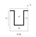
第1圖根據某些實施例描繪在基板102中結構108中鎢間隙填充的剖面視圖100。在傳統鎢間隙填充處理中,氮化鎢層首先沉積在基板的表面上,隨後為ALD鎢成核層及CVD鎢間隙填充。在本原理的方法及裝置下,PVD鎢襯墊104首先沉積在結構108中,且接著藉由CVD鎢/SS鎢處理沉積鎢塊體填充106。在某些實施例中,後續使用RTP處理以降低鎢塊體填充106的電阻率及應力。PVD鎢襯墊104在結構108中將具有合理的步階覆蓋。PVD沉積以例如氬或氪及類似者的環境稀有氣體以高離子化處理來進行。在PVD沉積處理期間的溫度可從大約室溫(攝氏~20度)至大約攝氏300度。1 depicts a
在氮化鈦層上的傳統CVD鎢間隙沉積以使用氟化鎢及乙硼烷(B2H6)/矽烷(SiH4)前驅物的鎢ALD成核及以WF6/H2作為前驅物鎢CVD塊體填充沉積而組成。在本原理的方法及裝置中,直接沉積鎢CVD塊體填充不具有鎢ALD成核層,而具有大約攝氏300度至大約攝氏500度的溫度及大約5 Torr至大約300 Torr的壓力。在處理中消除硼的使用允許使用RTP處理以強化在鎢中的電阻率及應力等級,而不會對鎢造成硼提升的黏著問題。退火溫度可為從大約攝氏700度至大約攝氏900度的範圍。退火時期可為大約60秒或更大。退火環境氣體可為氫或氬及類似者。在某些實施例中,溫度斜率可為從大約每秒攝氏30度至大約每秒攝氏100度的範圍或更多。Conventional CVD tungsten interstitial deposition on titanium nitride layers for tungsten ALD nucleation using tungsten fluoride and diborane (B2 H6 )/silane (SiH4 ) precursors and WF6 /H2 as precursors Tungsten CVD bulk fill deposition is formed. In the method and apparatus of the present principles, the direct deposited tungsten CVD bulk fill does not have a tungsten ALD nucleation layer, but has a temperature of about 300 degrees Celsius to about 500 degrees Celsius and a pressure of about 5 Torr to about 300 Torr. Eliminating the use of boron in the process allows the use of RTP processes to enhance resistivity and stress levels in tungsten without the boron-promoted adhesion problems with tungsten. The annealing temperature may range from about 700 degrees Celsius to about 900 degrees Celsius. The annealing period can be about 60 seconds or more. The annealing ambient gas can be hydrogen or argon and the like. In certain embodiments, the temperature slope may range from about 30 degrees Celsius per second to about 100 degrees Celsius per second or more.
第2圖根據某些實施例,為在基板上填充間隙之方法200。第3圖描繪根據方法200經間隙填充的基板302中結構304的剖面視圖300。在方塊202中,使用PVD處理在結構304上沉積鎢襯墊306。如先前所述,使用例如氬或氪及類似者的稀有氣體以高離子化進行PVD處理。PVD處理溫度可從大約室溫(攝氏~20度)至大約攝氏300度。鎢襯墊306的厚度取決於CD變化,且可為從大約40埃至大約200埃的範圍。在方塊204中,以與氫氣一起的WF6的前驅物使用CVD處理在結構304上沉積塊體填充鎢308,以不含硼的鎢填充結構304。CVD處理可在大約攝氏300度至大約攝氏500度的溫度下實行,且具有大約5 Torr至大約300 Torr的壓力。FIG. 2 is a
在可選方塊206中,於結構304上可實行RTP處理,以減少塊體填充鎢308的內部應力同時亦減少塊體填充鎢308的電阻率。在不使用硼下沉積塊體填充鎢308,且可避免與注入硼的鎢的RTP處理相關聯的問題。如上所述,退火溫度可為從大約攝氏700度至大約攝氏900的範圍。退火時期可為大約60秒或更大。退火環境氣體可為氫或氬及類似者。在某些實施例中,溫度斜率可為從大約每秒攝氏30度至大約每秒攝氏100度的範圍或更多。方法200對具有小於8:1的深寬比的結構作用良好。發明人已發現若高深寬比太大(例如,8:1至15:1),則歸因於在PVD鎢沉積期間懸垂312的形成且歸因於塊體填充鎢308的保形天性,在塊體填充鎢308中可出現空洞310。為了解決在結構304中空洞的形成,發明人已發現如在第4及6圖中所述的替代方法,而可用於更高深寬比。In
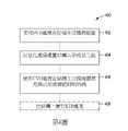
第4圖根據某些實施例,為使用氮化處理在基板302上填充間隙之方法400。第5圖描繪根據方法400經間隙填充不具空洞的結構304的剖面視圖500。在方塊402中,使用PVD處理在結構304上沉積鎢襯墊306。鎢襯墊306的厚度取決於CD變化,且可為從大約40埃至大約200埃的範圍。鎢襯墊306作用為用於後續塊體填充的成核層。使用例如氬或氪及類似者的稀有氣體以高離子化進行PVD處理。PVD處理溫度可從大約室溫(攝氏~20度)至大約攝氏300度。在方塊404中,以氮化處理處置結構304以形成氮化鎢506。在氮化處理中,氮自由基僅在或接近結構304的頂部表面510上形成氮化鎢。氮化鎢造成後續CVD鎢沉積在頂部表面510上具有培養延遲,但CVD鎢沉積從底部512且在結構304的內側向上將具有正常成長。氮化處理導致CVD鎢沉積的底部向上或超級保形沉積行為,以減少在結構304的內側形成空洞。在某些實施例中,氮化處理包括以大約1 sccm至大約20 sccm的速率流動氮而具有大約2秒至大約20秒的時期。可使用本端或遠端電漿源。FIG. 4 is a
在方塊406中,使用CVD處理在結構304上沉積塊體填充鎢508,以形成接縫抑制的鎢。CVD處理與氫氣一起使用WF6的前驅物,以形成不含硼的鎢。CVD處理可在大約攝氏300度至大約攝氏500度的溫度下實行,且具有大約5 Torr至大約300 Torr的壓力。在可選方塊408中,可在結構304上實行RTP處理,以減少塊體填充鎢508的內部應力,同時亦減少塊體填充鎢508的電阻率。在不使用硼下沉積塊體填充鎢508,且可避免與注入硼的鎢的RTP處理相關聯的問題。退火溫度可為從大約攝氏700度至大約攝氏900的範圍。退火時期可為大約60秒或更大。退火環境氣體可為氫或氬及類似者。在某些實施例中,溫度斜率可為從大約每秒攝氏30度至大約每秒攝氏100度的範圍或更多。In
第6圖根據某些實施例,為使用ALD成核層處理在基板302上填充間隙之方法。第7圖描繪根據方法600使用ALD成核層經間隙填充的結構304的剖面視圖700。在方塊602中,使用PVD處理在結構304上沉積鎢襯墊306。鎢襯墊306的厚度取決於CD變化,且可為從大約40埃至大約200埃的範圍。使用例如氬或氪及類似者的稀有氣體以高離子化進行PVD處理。PVD處理溫度可從大約室溫(攝氏~20度)至大約攝氏300度。在方塊604中,使用ALD處理在結構304上形成薄的鎢成核層702。薄的鎢成核層702的厚度可為從大約10埃至大約60埃。在氮化處置之前施加鎢成核層,以幫助在頂部表面710上培養延遲。後續沉積的塊體填充鎢的內部應力位準將維持相同,但後續沉積的塊體填充鎢的電阻率相較於不具ALD處理的處理可增加大約10%。FIG. 6 is a method of filling gaps on
在方塊606中,以氮化處理處置結構304以形成氮化鎢層706。在氮化處理中,氮自由基僅在或接近結構304的頂部表面710上形成氮化鎢。氮化鎢層706造成後續CVD鎢沉積在頂部表面710上具有培養延遲,但CVD鎢沉積從底部712且在結構304的內側向上將具有正常成長。氮化處理導致CVD鎢沉積的底部向上或超級保形沉積行為,以減少在結構304的內側形成空洞。在某些實施例中,氮化處理包括以大約1 sccm至大約20 sccm的速率流動氮而具有大約2秒至大約20秒的時期。可使用本端或遠端電漿源。在方塊608中,使用CVD處理在結構304上沉積塊體填充鎢708,以形成接縫抑制的鎢。CVD處理與氫氣一起使用WF6的前驅物。CVD處理可在大約攝氏300度至大約攝氏500度的溫度下實行,且具有大約5 Torr至大約300 Torr的壓力。In
在以上所述的方法的某些實施例中即使不併入RTP處理,鎢塊體填充的內部應力(以MPa量測)在傳統處理上將減少大約10%(約2000埃的膜厚度)至大約50%(500埃或更少的膜厚度)或更多,對更薄的膜具有最大的減少。同時,鎢塊體填充的電阻率在傳統處理上減少大約30%至大約40%或更多。在以上所述的方法的某些實施例中額外的RTP處理對具有熱處置的傳統處理進一步減少內部應力且進一步降低鎢塊體填充的電阻率。RTP處理對傳統處理的所有厚度減少鎢塊體填充的內部應力從大約45%至大約55%或更多。RTP處理對傳統處理減少鎢塊體填充的電阻率從大約35%至大約45%。此外,本原理的方法在如同傳統處理中使用硼衍生物的退火處理之後,不具有降級的黏著問題。Even without incorporating an RTP process in certain embodiments of the method described above, the internal stress (measured in MPa) of the tungsten bulk fill will be reduced by about 10% (film thickness of about 2000 angstroms) over conventional processes to About 50% (film thickness of 500 angstroms or less) or more, with the greatest reduction for thinner films. At the same time, the resistivity of the tungsten bulk fill is reduced by about 30% to about 40% or more over conventional processing. The additional RTP treatment in certain embodiments of the methods described above further reduces internal stress and further reduces the resistivity of the tungsten bulk fill over conventional treatments with thermal treatment. The RTP process reduces the internal stress of the tungsten bulk fill from about 45% to about 55% or more over all thicknesses of the conventional process. The RTP process reduces the resistivity of the bulk tungsten fill from about 35% to about 45% over the conventional process. Furthermore, the method of the present principles does not suffer from degraded sticking issues after annealing treatments using boron derivatives as in conventional treatments.
根據本原理的實施例可在硬體、韌體、軟體或其任何結合中實施。實施例亦可實施作為使用一或更多電腦可讀取媒體儲存的指令,而可藉由一或更多處理器讀取且執行。電腦可讀取媒體可包括以藉由機器(例如,計算平台或在一或更多計算平台上運行的「虛擬機器」)可讀取的形式用於儲存或傳送資訊的任何機制。舉例而言,電腦可讀取媒體可包括揮發及非揮發記憶體的任何適合的形式。在某些實施例中,電腦可讀取媒體可包括非暫態電腦可讀取媒體。Embodiments in accordance with the present principles may be implemented in hardware, firmware, software, or any combination thereof. Embodiments can also be implemented as instructions stored using one or more computer-readable media, readable and executable by one or more processors. A computer-readable medium may include any mechanism for storing or transmitting information in a form readable by a machine (eg, a computing platform or a "virtual machine" running on one or more computing platforms). For example, computer-readable media may include any suitable form of volatile and non-volatile memory. In some embodiments, the computer-readable medium may comprise a non-transitory computer-readable medium.
儘管以上導向本原理的實施例,可衍生本原理的其他及進一步實施例而不會悖離其基本範疇。Although the above is directed to embodiments of the present principles, other and further embodiments of the present principles can be derived without departing from the basic scope thereof.
100:視圖 102:基板 104:鎢襯墊 106:塊體填充 108:結構 200:方法 202:方塊 204:方塊 206:方塊 300:視圖 302:基板 304:結構 306:鎢襯墊 308:塊體填充鎢 310:空洞 312:懸垂 400:方法 402:方塊 404:方塊 406:方塊 408:方塊 500:視圖 506:氮化鎢 508:塊體填充鎢 510:頂部表面 600:方法 602:方塊 604:方塊 606:方塊 608:方塊 700:視圖 702:層 706:氮化鎢層 708:塊體填充鎢 710:頂部表面 712:底部100: View 102: Substrate 104: Tungsten Pad 106: Block Fill 108: Structure 200: Method 202: Blocks 204: Blocks 206: Blocks 300: view 302: Substrate 304: Structure 306: Tungsten Pad 308: Bulk Filled Tungsten 310: Hollow 312: Drape 400: Method 402: Square 404: Square 406: Square 408: Square 500: view 506: Tungsten Nitride 508: Bulk Filled Tungsten 510: Top Surface 600: Method 602: Blocks 604: Square 606: Blocks 608: Square 700: View 702: Layer 706: Tungsten nitride layer 708: Bulk Filled Tungsten 710: Top Surface 712: Bottom
以上簡要概述且以下更詳細討論的本原理的實施例可藉由參考本在隨附圖式中描繪的本原理的圖示實施例而理解。然而,隨附圖式僅圖示本原理的通常實施例,且因此不應考量為範疇之限制,因為本原理可認可其他均等效果的實施例。Embodiments of the present principles, briefly summarized above and discussed in greater detail below, can be understood by reference to the illustrative embodiments of the present principles depicted in the accompanying drawings. However, the accompanying drawings illustrate only general embodiments of the present principles and are therefore not to be considered limiting in scope, for the present principles may admit to other equally effective embodiments.
第1圖根據本原理的某些實施例,描繪在基板上於結構中的鎢間隙填充的剖面視圖。FIG. 1 depicts a cross-sectional view of a tungsten gapfill in a structure on a substrate in accordance with some embodiments of the present principles.
第2圖根據本原理的某些實施例,為在基板上填充間隙之方法。FIG. 2 is a method of filling gaps in a substrate, in accordance with some embodiments of the present principles.
第3圖根據本原理的某些實施例,描繪經間隙填充的高深寬比結構的剖面視圖。3 depicts a cross-sectional view of a gap-filled high aspect ratio structure in accordance with certain embodiments of the present principles.
第4圖根據本原理的某些實施例,為使用氮化處理在基板上填充間隙之方法。FIG. 4 is a method of filling gaps in a substrate using a nitridation process, according to some embodiments of the present principles.
第5圖根據本原理的某些實施例,描繪經間隙填充不具空洞的高深寬比結構的剖面視圖。5 depicts a cross-sectional view of a gap-filled high aspect ratio structure without voids, in accordance with certain embodiments of the present principles.
第6圖根據本原理的某些實施例,為使用ALD成核層在基板上填充間隙之方法。FIG. 6 is a method of filling gaps in a substrate using an ALD nucleation layer, according to some embodiments of the present principles.
第7圖根據本原理的某些實施例,描繪使用ALD成核層經間隙填充的高深寬比結構之剖面視圖。7 depicts a cross-sectional view of a gap-filled high aspect ratio structure using an ALD nucleation layer, in accordance with certain embodiments of the present principles.
為了促進理解,已儘可能地使用相同的元件符號代表共通圖式中相同的元件。圖式並未按照規模繪製,且為了清楚可簡化。一個實施例的元件及特徵可有益地併入其他實施例中而無須進一步說明。To facilitate understanding, the same reference numerals have been used wherever possible to represent the same elements in the common figures. The drawings are not drawn to scale and may be simplified for clarity. Elements and features of one embodiment may be beneficially incorporated into other embodiments without further description.
國內寄存資訊(請依寄存機構、日期、號碼順序註記) 無 國外寄存資訊(請依寄存國家、機構、日期、號碼順序註記) 無Domestic storage information (please note in the order of storage institution, date and number) none Foreign deposit information (please note in the order of deposit country, institution, date and number) none
100:視圖100: View
102:基板102: Substrate
104:鎢襯墊104: Tungsten Pad
106:塊體填充106: Block Fill
108:結構108: Structure
Claims (20)
Translated fromChineseApplications Claiming Priority (2)
| Application Number | Priority Date | Filing Date | Title |
|---|---|---|---|
| US17/082,602 | 2020-10-28 | ||
| US17/082,602US11798845B2 (en) | 2020-10-28 | 2020-10-28 | Methods and apparatus for low resistivity and stress tungsten gap fill |
Publications (1)
| Publication Number | Publication Date |
|---|---|
| TW202223154Atrue TW202223154A (en) | 2022-06-16 |
Family
ID=81256759
Family Applications (1)
| Application Number | Title | Priority Date | Filing Date |
|---|---|---|---|
| TW110137930ATW202223154A (en) | 2020-10-28 | 2021-10-13 | Methods and apparatus for low resistivity and stress tungsten gap fill |
Country Status (6)
| Country | Link |
|---|---|
| US (2) | US11798845B2 (en) |
| JP (1) | JP2023548256A (en) |
| KR (1) | KR20230092821A (en) |
| CN (1) | CN115023792A (en) |
| TW (1) | TW202223154A (en) |
| WO (1) | WO2022093465A1 (en) |
Families Citing this family (4)
| Publication number | Priority date | Publication date | Assignee | Title |
|---|---|---|---|---|
| KR20230127801A (en)* | 2022-02-25 | 2023-09-01 | 삼성전자주식회사 | Semiconductor device and method of fabricating semiconductor device |
| WO2024030248A1 (en)* | 2022-08-04 | 2024-02-08 | Applied Materials, Inc. | Methods for forming multi-tier tungsten features |
| TW202412080A (en)* | 2022-09-09 | 2024-03-16 | 美商應用材料股份有限公司 | Integrated pvd tungsten liner and seamless cvd tungsten fill |
| WO2025110419A1 (en)* | 2023-11-20 | 2025-05-30 | 주식회사 원익아이피에스 | Method for forming metal thin film |
Family Cites Families (14)
| Publication number | Priority date | Publication date | Assignee | Title |
|---|---|---|---|---|
| KR940010158B1 (en)* | 1991-07-09 | 1994-10-22 | 한국과학기술연구원 | Tungsten film depositing method using pecvd |
| TW350933B (en)* | 1996-11-23 | 1999-01-21 | Lg Semicon Co Ltd | X-ray absorbing layer in the X-ray mask and the manufacturing method |
| EP1094504A3 (en)* | 1999-10-18 | 2001-08-22 | Applied Materials, Inc. | PVD-IMP tungsten and tungsten nitride as a liner, barrier, and/or seed layer |
| US6936538B2 (en) | 2001-07-16 | 2005-08-30 | Applied Materials, Inc. | Method and apparatus for depositing tungsten after surface treatment to improve film characteristics |
| US6492281B1 (en)* | 2000-09-22 | 2002-12-10 | Advanced Micro Devices, Inc. | Method of fabricating conductor structures with metal comb bridging avoidance |
| US9159571B2 (en) | 2009-04-16 | 2015-10-13 | Lam Research Corporation | Tungsten deposition process using germanium-containing reducing agent |
| US10256142B2 (en)* | 2009-08-04 | 2019-04-09 | Novellus Systems, Inc. | Tungsten feature fill with nucleation inhibition |
| US9129945B2 (en) | 2010-03-24 | 2015-09-08 | Applied Materials, Inc. | Formation of liner and barrier for tungsten as gate electrode and as contact plug to reduce resistance and enhance device performance |
| KR102100520B1 (en)* | 2012-03-27 | 2020-04-14 | 노벨러스 시스템즈, 인코포레이티드 | Tungsten feature fill with nucleation inhibition |
| US9589808B2 (en) | 2013-12-19 | 2017-03-07 | Lam Research Corporation | Method for depositing extremely low resistivity tungsten |
| US9685370B2 (en) | 2014-12-18 | 2017-06-20 | Globalfoundries Inc. | Titanium tungsten liner used with copper interconnects |
| US10043670B2 (en) | 2015-10-22 | 2018-08-07 | Applied Materials, Inc. | Systems and methods for low resistivity physical vapor deposition of a tungsten film |
| US9735015B1 (en) | 2016-12-05 | 2017-08-15 | United Microelectronics Corporation | Fabricating method of semiconductor structure |
| JP7705347B2 (en)* | 2018-12-05 | 2025-07-09 | ラム リサーチ コーポレーション | Void-free, low stress filling |
- 2020
- 2020-10-28USUS17/082,602patent/US11798845B2/enactiveActive
- 2021
- 2021-09-28WOPCT/US2021/052336patent/WO2022093465A1/ennot_activeCeased
- 2021-09-28KRKR1020227024380Apatent/KR20230092821A/enactivePending
- 2021-09-28JPJP2022542675Apatent/JP2023548256A/enactivePending
- 2021-09-28CNCN202180009088.1Apatent/CN115023792A/enactivePending
- 2021-10-13TWTW110137930Apatent/TW202223154A/enunknown
- 2022
- 2022-07-05USUS17/857,341patent/US12094773B2/enactiveActive
Also Published As
| Publication number | Publication date |
|---|---|
| WO2022093465A1 (en) | 2022-05-05 |
| JP2023548256A (en) | 2023-11-16 |
| US20220336274A1 (en) | 2022-10-20 |
| US12094773B2 (en) | 2024-09-17 |
| KR20230092821A (en) | 2023-06-26 |
| CN115023792A (en) | 2022-09-06 |
| US11798845B2 (en) | 2023-10-24 |
| US20220130724A1 (en) | 2022-04-28 |
Similar Documents
| Publication | Publication Date | Title |
|---|---|---|
| TW202223154A (en) | Methods and apparatus for low resistivity and stress tungsten gap fill | |
| US5498768A (en) | Process for forming multilayer wiring | |
| US7521379B2 (en) | Deposition and densification process for titanium nitride barrier layers | |
| US6927163B2 (en) | Method and apparatus for manufacturing a barrier layer of semiconductor device | |
| JP4001509B2 (en) | Method for forming diffusion barrier film of semiconductor element | |
| US11967525B2 (en) | Selective tungsten deposition at low temperatures | |
| US20090026626A1 (en) | Method for fabricating semiconductor device and semiconductor device | |
| CN110911347A (en) | Semiconductor structure and forming method thereof | |
| CN102054758A (en) | Method for forming tungsten plug | |
| JP4127359B2 (en) | Method for manufacturing integrated circuit device | |
| JP4804725B2 (en) | Method for forming conductive structure of semiconductor device | |
| CN100576495C (en) | Fabrication method of interconnect structure | |
| JPH1032248A (en) | Formation of tungsten film | |
| JP7552984B2 (en) | Selective tungsten deposition at low temperatures | |
| CN109065495B (en) | Method for forming fluorine-free tungsten metal layer in tungsten filled groove structure | |
| US6787466B2 (en) | High throughout process for the formation of a refractory metal nucleation layer | |
| JP2002057125A (en) | Method of forming metal wiring | |
| KR100753416B1 (en) | Manufacturing method of semiconductor device | |
| KR20050106916A (en) | Method for manufacturing semiconductor device with diffusion barrier | |
| JP2024527979A (en) | Enhanced stress conditioning and interfacial adhesion for tungsten (W) gap filling | |
| TW202431541A (en) | Plasma treatment of barrier and liner layers | |
| TW202320185A (en) | Methods and apparatus for tungsten gap fill | |
| KR20000043053A (en) | Metalization of semiconductor device | |
| KR19980060642A (en) | Titanium Nitride Film Formation Method | |
| KR20010108839A (en) | Method for forming plug in semiconductor device |