TW202222656A - Carrier tapes for microelectronic devices and related methods - Google Patents
Carrier tapes for microelectronic devices and related methodsDownload PDFInfo
- Publication number
- TW202222656A TW202222656ATW110114374ATW110114374ATW202222656ATW 202222656 ATW202222656 ATW 202222656ATW 110114374 ATW110114374 ATW 110114374ATW 110114374 ATW110114374 ATW 110114374ATW 202222656 ATW202222656 ATW 202222656A
- Authority
- TW
- Taiwan
- Prior art keywords
- carrier tape
- recesses
- recess
- tape
- microelectronic device
- Prior art date
Links
- 238000004377microelectronicMethods0.000titleclaimsabstractdescription89
- 238000000034methodMethods0.000titleclaimsdescription53
- 239000000463materialSubstances0.000claimsabstractdescription54
- 230000004044responseEffects0.000claimsabstractdescription30
- 238000010438heat treatmentMethods0.000claimsdescription30
- 239000000853adhesiveSubstances0.000claimsdescription11
- 230000001070adhesive effectEffects0.000claimsdescription11
- 238000001816coolingMethods0.000claimsdescription11
- 230000007423decreaseEffects0.000claimsdescription10
- 230000002093peripheral effectEffects0.000claimsdescription3
- 230000000717retained effectEffects0.000claimsdescription3
- 230000002441reversible effectEffects0.000claimsdescription3
- 239000004065semiconductorSubstances0.000description158
- 230000008569processEffects0.000description11
- 230000009471actionEffects0.000description10
- 230000008602contractionEffects0.000description7
- 230000007704transitionEffects0.000description7
- 230000000670limiting effectEffects0.000description6
- 238000003860storageMethods0.000description5
- 230000000712assemblyEffects0.000description3
- 238000000429assemblyMethods0.000description3
- 238000004519manufacturing processMethods0.000description3
- 230000031070response to heatEffects0.000description3
- 238000007792additionMethods0.000description2
- 238000005452bendingMethods0.000description2
- 230000008901benefitEffects0.000description2
- 230000015572biosynthetic processEffects0.000description2
- 238000011109contaminationMethods0.000description2
- 238000013461designMethods0.000description2
- 230000000694effectsEffects0.000description2
- 238000001125extrusionMethods0.000description2
- 230000006870functionEffects0.000description2
- 238000001746injection mouldingMethods0.000description2
- 238000003780insertionMethods0.000description2
- 230000037431insertionEffects0.000description2
- 239000000758substrateSubstances0.000description2
- 238000012360testing methodMethods0.000description2
- 238000004804windingMethods0.000description2
- 2380000101463D printingMethods0.000description1
- 239000004793PolystyreneSubstances0.000description1
- 230000001464adherent effectEffects0.000description1
- 239000002313adhesive filmSubstances0.000description1
- 230000006399behaviorEffects0.000description1
- 239000002131composite materialSubstances0.000description1
- 238000005336crackingMethods0.000description1
- 230000003247decreasing effectEffects0.000description1
- 238000012217deletionMethods0.000description1
- 230000037430deletionEffects0.000description1
- 238000011161developmentMethods0.000description1
- 238000005553drillingMethods0.000description1
- 238000005530etchingMethods0.000description1
- 230000001747exhibiting effectEffects0.000description1
- 238000003754machiningMethods0.000description1
- 229910052751metalInorganic materials0.000description1
- 239000002184metalSubstances0.000description1
- 229910001092metal group alloyInorganic materials0.000description1
- 150000002739metalsChemical class0.000description1
- 238000003801millingMethods0.000description1
- 238000012986modificationMethods0.000description1
- 230000004048modificationEffects0.000description1
- 229920000642polymerPolymers0.000description1
- 229920002223polystyrenePolymers0.000description1
- 238000012545processingMethods0.000description1
- 230000002829reductive effectEffects0.000description1
- 238000007493shaping processMethods0.000description1
- 235000012773wafflesNutrition0.000description1
- 239000002699waste materialSubstances0.000description1
Images


Classifications
- H—ELECTRICITY
- H01—ELECTRIC ELEMENTS
- H01L—SEMICONDUCTOR DEVICES NOT COVERED BY CLASS H10
- H01L21/00—Processes or apparatus adapted for the manufacture or treatment of semiconductor or solid state devices or of parts thereof
- H01L21/67—Apparatus specially adapted for handling semiconductor or electric solid state devices during manufacture or treatment thereof; Apparatus specially adapted for handling wafers during manufacture or treatment of semiconductor or electric solid state devices or components ; Apparatus not specifically provided for elsewhere
- H01L21/683—Apparatus specially adapted for handling semiconductor or electric solid state devices during manufacture or treatment thereof; Apparatus specially adapted for handling wafers during manufacture or treatment of semiconductor or electric solid state devices or components ; Apparatus not specifically provided for elsewhere for supporting or gripping
- H01L21/6835—Apparatus specially adapted for handling semiconductor or electric solid state devices during manufacture or treatment thereof; Apparatus specially adapted for handling wafers during manufacture or treatment of semiconductor or electric solid state devices or components ; Apparatus not specifically provided for elsewhere for supporting or gripping using temporarily an auxiliary support
Landscapes
- Engineering & Computer Science (AREA)
- Physics & Mathematics (AREA)
- Condensed Matter Physics & Semiconductors (AREA)
- General Physics & Mathematics (AREA)
- Manufacturing & Machinery (AREA)
- Computer Hardware Design (AREA)
- Microelectronics & Electronic Packaging (AREA)
- Power Engineering (AREA)
- Packages (AREA)
- Packaging Frangible Articles (AREA)
Abstract
Description
Translated fromChinese本發明總體上係關於用於在卷軸上儲存諸如半導體晶粒等之微電子裝置以進行運輸以及與取置機一起使用之承載帶及相關方法。更具體言之,本發明係關於承載帶,其可減少在將微電子裝置自承載帶移除期間對微電子裝置造成損壞的可能性,可需要更少的材料及資源來實現將微電子裝置臨時儲存在承載帶上,並且可提高在將半導體晶粒自承載帶移除期間之拾取及置放過程的準確性。The present invention generally relates to carrier tapes and related methods for storing microelectronic devices, such as semiconductor dies, on reels for shipping and use with pick-and-place machines. More specifically, the present invention relates to carrier tapes that reduce the likelihood of damage to microelectronic devices during removal of the microelectronic devices from the carrier tape, requiring fewer materials and resources to implement microelectronic devices. Temporarily stored on the carrier tape and can improve the accuracy of the pick and place process during removal of the semiconductor die from the carrier tape.
當將諸如半導體晶粒等之微電子裝置置放至諸如另一半導體晶粒、晶圓或其他塊體半導體基板、中介層或印刷電路板(PCB)等之另一組件上時,可將半導體晶粒以呈帶-卷組態之方式設置在具有其他相互縱向間隔之半導體晶粒之承載帶上。例如,半導體晶粒可收容在承載帶中之凹部或間隙中,並且可利用黏附材料習知地保持在此等凹部或間隙中。一種選用的可撓性蓋帶可用於覆蓋承載帶之一或多個側面上之凹部或間隙,並且可提供一個具有黏附劑之表面。其中黏附有半導體晶粒之承載帶可與選用的蓋帶一同捲至卷軸上用於儲存、運輸等。一旦到達移除及置放半導體晶粒之時間,可移除選用的蓋帶,並將半導體晶粒自凹部或間隙中提起(例如,利用取置機)以置放並固定在另一組件上。此種帶及卷軸總成可用於所謂的「已知良好晶粒」(KGD)之運輸及處置,該等「已知良好晶粒」(KGD)係經測試及檢核(即,特性化)為判定適合於特定應用之半導體晶粒,如包含多個堆疊記憶體晶粒之記憶體裝置等。When a microelectronic device, such as a semiconductor die, is placed on another component, such as another semiconductor die, a wafer or other bulk semiconductor substrate, an interposer, or a printed circuit board (PCB), a semiconductor can be placed The dies are arranged in a tape-and-reel configuration on a carrier tape with other mutually longitudinally spaced semiconductor dies. For example, semiconductor dies may be housed in recesses or gaps in the carrier tape, and may be conventionally held in such recesses or gaps using an adhesive material. An optional flexible cover tape may be used to cover recesses or gaps on one or more sides of the carrier tape and may provide a surface with an adhesive. The carrier tape with the semiconductor die attached therein can be rolled onto a reel together with the optional cover tape for storage and transportation. Once it is time to remove and place the semiconductor die, the optional cover tape can be removed, and the semiconductor die can be lifted out of the recess or gap (eg, using a pick-and-placer) to place and secure on another component . Such tape and reel assemblies can be used for the transportation and handling of so-called "known good dies" (KGD) that are tested and inspected (ie, characterized) To determine which semiconductor die is suitable for a particular application, such as a memory device comprising a plurality of stacked memory dies, etc.
在一些實施例中,用於微電子裝置的承載帶可包括細長帶體,細長帶體包括凹部。凹部可被設定大小、塑形及定位以在各別凹部中收容各別微電子裝置。帶體之材料及帶體之鄰近凹部之部分之組態的熱膨脹係數可允許帶體之材料回應於帶體之溫度升高而膨脹,並擴大由帶體之溫度升高之部分包圍的凹部之至少一個尺寸維度。此膨脹及擴大可允許凹部收容微電子裝置,並且回應於該部分之溫度自經升高溫度之降低而收縮並使帶體之鄰近凹部之至少兩個相對表面與該微電子裝置接觸並固持該微電子裝置。In some embodiments, a carrier tape for a microelectronic device can include an elongated tape body that includes a recess. The recesses can be sized, shaped and positioned to receive individual microelectronic devices in respective recesses. The coefficient of thermal expansion of the material of the belt and the configuration of the portion of the belt adjacent to the recess may allow the material of the belt to expand in response to the temperature increase of the belt and to expand the size of the recess surrounded by the portion of the belt with increased temperature. At least one dimension dimension. This expansion and expansion may allow the recess to accommodate the microelectronic device and, in response to a decrease in temperature of the portion from the elevated temperature, contract and bring at least two opposing surfaces of the tape adjacent the recess into contact with and hold the microelectronic device. microelectronic devices.
在其他實施例中,在承載帶上儲存微電子裝置之方法可涉及:將承載帶體之一部分自收縮狀態加熱至膨脹狀態,以使承載體中之至少一個凹部在至少一個尺寸維度上膨脹至足以收容微電子裝置。微電子裝置可至少部分地置放在至少一個凹部內。可冷卻(如主動地、被動地)該承載帶體之部分,以使至少一個凹部在該至少一個尺寸維度上收縮並將置放在其中之微電子裝置固定,承載帶體之部分鄰近該凹部。In other embodiments, a method of storing microelectronic devices on a carrier tape may involve heating a portion of the carrier tape body from a contracted state to an expanded state to expand at least one recess in the carrier body in at least one dimensional dimension to Sufficient to accommodate microelectronic devices. The microelectronic device may be placed at least partially within the at least one recess. The portion of the carrier tape may be cooled (eg, actively, passively) to shrink at least one recess in the at least one dimensional dimension and secure the microelectronic device placed therein, the portion of the carrier tape adjacent to the recess .
在其他實施例中,處置微電子裝置之方法可涉及:回應於加熱包括承載帶之至少一些凹部的承載帶之至少一部分,將該至少一些凹部自收縮狀態膨脹至膨脹狀態,以使承載帶之界定該至少一些凹部中之各別凹部之至少一個表面與位於該至少一些凹部中之各別凹部內之微電子裝置脫離接觸。可將微電子裝置自該至少一些凹部中之各別凹部中移除。In other embodiments, a method of handling a microelectronic device may involve: in response to heating at least a portion of a carrier tape including at least some recesses of the carrier tape, expanding the at least some recesses from a contracted state to an expanded state to cause the carrier tape At least one surface defining a respective one of the at least some recesses is out of contact with a microelectronic device located within a respective one of the at least some recesses. The microelectronic device can be removed from a respective one of the at least some of the recesses.
優先權主張priority claim
本申請案主張2020年12月1日申請之名為「用於微電子裝置的承載帶及相關方法(Carrier Tapes for Microelectronic Devices and Related Methods)」的美國臨時專利申請案第63/119,946號之申請日的權益。This application claims US Provisional Patent Application Serial No. 63/119,946, filed on December 1, 2020, entitled "Carrier Tapes for Microelectronic Devices and Related Methods" day's rights.
在本發明中呈現之圖示並不意謂係任何特定承載帶、卷軸、半導體晶粒或其他微電子裝置、卡盤、取置設備或其組件之實際視圖,而僅僅係用於描述說明性實施例之理想化表示。因此,圖式未必按比例繪製。The illustrations presented in this disclosure are not meant to be actual views of any particular carrier tape, reel, semiconductor die or other microelectronic device, chuck, pick and place equipment or components thereof, but are merely intended to describe illustrative implementations An idealized representation of an example. Accordingly, the drawings are not necessarily drawn to scale.
所揭示之實施例總體上係關於承載帶,其可減少在將微電子裝置自承載帶移除期間對如呈半導體晶粒形式之微電子裝置造成損壞的可能性,可需要更少的材料及資源來實現將半導晶粒儲存在承載帶上,並且可提高在將半導體晶粒自承載帶移除期間之拾取及置放過程的準確性。更具體言之,揭示了用於臨時儲存半導體晶粒之承載帶之實施例,該實施例可利用溫度引起之膨脹及收縮而非黏附材料來將半導體晶粒臨時固定在承載帶中之凹部中。例如,本文中所揭示之承載帶及承載帶中之凹部之相關形狀可藉由承載帶之接觸表面與半導體晶粒或疊加於半導體晶粒表面之突出特徵之間的摩擦將半導體晶粒保持在凹部中。The disclosed embodiments relate generally to carrier tapes, which can reduce the likelihood of damage to microelectronic devices, such as in the form of semiconductor dies, during removal of microelectronic devices from the carrier tape, may require less material, and resources to enable storage of the semiconductor die on the carrier tape and can improve the accuracy of the pick and place process during removal of the semiconductor die from the carrier tape. More specifically, embodiments of carrier tapes for temporary storage of semiconductor dies are disclosed that utilize temperature-induced expansion and contraction, rather than adhesive materials, to temporarily hold semiconductor dies in recesses in the carrier tape . For example, the carrier tapes and associated shapes of recesses in the carrier tape disclosed herein may hold the semiconductor die in place by friction between the contact surface of the carrier tape and the semiconductor die or protruding features superimposed on the surface of the semiconductor die. in the recess.
如本文中所使用,關於給定參數、性質或條件之術語「實質上」及「約」在一定程度上意謂並且包括:一般熟習此項技術者將理解的是給定參數、性質或條件滿足一定程度內之變化,如在可接受之製造公差內。例如,實質上為或約為指定值之參數可係指定值之至少約90%、指定值之至少約95%、指定值之至少約99%,或甚至為指定值之至少約99.9%。As used herein, the terms "substantially" and "about" in reference to a given parameter, property or condition mean and include to the extent that a given parameter, property or condition will be understood by those of ordinary skill in the art Variations are met within a certain degree, such as within acceptable manufacturing tolerances. For example, a parameter that is substantially at or about the specified value can be at least about 90% of the specified value, at least about 95% of the specified value, at least about 99% of the specified value, or even at least about 99.9% of the specified value.
如本文中所使用,術語「凹部」在承載帶或帶體之上下文中不僅包括具有側壁及底面之空腔,而且亦包括僅具有側壁並完全延伸穿過承載帶或帶體之狹槽或間隙。As used herein, the term "recess" in the context of a carrier tape or body includes not only a cavity having side walls and a bottom surface, but also a slot or gap that has only side walls and extends completely through the carrier tape or body .
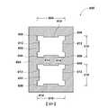
圖1係根據本發明之承載帶100之一部分的截面側視圖。承載帶100可包括:例如具有自承載帶100之第一主表面104向承載帶100之第二主表面106延伸的至少一個凹部102之條狀或片狀材料。更具體言之,承載帶100可包括:沿承載帶100之縱向長度分佈之一系列或圖案之等間距凹部102,至少一些凹部102被設定大小、塑形及定位以支撐其中之各別半導體晶粒。在一些實施例中,如圖1所示之實施例,沿著承載帶100之至少實質上整個縱向長度,第二主表面106可係至少實質上連續的,並且第一主表面104可係不連續的,第一主表面104中之中斷至少由凹部102之口部形成。此組態可表示用於形成根據本發明之承載帶100之某些製程,例如注射模製或擠壓製程,隨後進行材料移除製程(例如機加工、銑削、雷射鑽孔、蝕刻)。1 is a cross-sectional side view of a portion of a
至少一些凹部102中之每一凹部可被設定大小、塑形及定位以支撐其中之各別半導體晶粒。在一些實施例中,凹部102可包括底面108及兩或多個側面110,底面108被定位成與半導體晶粒之主表面接觸並支撐該主表面,側面110被定位成:當各別凹部處於收縮狀態時,與半導體晶粒之各別側面接觸並形成摩擦配合。更具體言之,底面108及側面110可界定大體上成直角矩形稜柱形之凹部102,該凹部102被設定大小以:當凹部102處於膨脹狀態時,使半導體晶粒(例如利用間隙配合)進入凹部102,以及與半導體晶粒之一些側面之至少一些部分(例如利用干涉配合)接觸,使得當凹部102處於收縮狀態時,將半導體晶粒臨時固定在凹部102中。Each of at least some of the
凹部102之大小及形狀之公差以及承載帶100之材料之熱膨脹係數(CTE)可允許凹部102實現以下行為:回應於施加至最接近每一凹部102之承載帶100之熱而膨脹以收容各別半導體晶粒,並且回應於熱移除而收縮以與收容在此凹部102中之各別半導體晶粒接觸。例如,凹部102之特定大小及形狀可與預期收容在凹部102中之半導體晶粒之平均大小及形狀或特定大小及形狀相同,凹部102之特定公差小於回應於加熱及後續熱移除而達到之膨脹及收縮的程度。更具體言之,凹部102之大小及形狀之公差可在膨脹及收縮程度之約25%至約50%之間,該膨脹及收縮程度係由給定凹部之長度及寬度回應於給定量值之加熱及後續熱移除而達到的。作為特定非限制性實例,凹部102之大小及形狀之公差可在約+/-20微米至約+/-35微米之間(例如約+/-25微米、約+/-30微米),並且回應於受熱及後續熱移除而達到之膨脹及收縮程度可在約60微米至約80微米之間(例如約70微米)。Tolerances in the size and shape of the
承載帶100之材料之熱膨脹係數(CTE)可例如約為3或更大。更具體言之,承載帶100之材料之熱膨脹係數(CTE)可例如在約5至約80之間。作為特定非限制性實例,承載帶100之材料之熱膨脹係數(CTE)可在約10至約70之間(例如12、15、18、20、25)。承載帶100之材料可係例如聚合物、金屬、金屬合金或複合材料。在一些實施例中,可利用習知用於承載帶之材料來形成根據本發明之承載帶100。作為特定非限制性實例,承載帶100之材料可係碳酸聚苯乙烯材料,例如在由明尼蘇達(Minnesota)之Advantek of Eden Prairie提供的SURFTAPE®承載帶中使用之材料。承載帶100之所有表面可完全不含黏附材料,特別係界定凹部102之如底面108及側面110等之表面。承載帶100可依靠例如除黏附力之外的力將半導體晶粒保持在各別凹部102內。更具體言之,圖1、圖2及圖3所示之承載帶100之實施例可利用一或兩對界定凹部102之相對側面110之間的摩擦力。在根據本發明之承載帶之其他實施例中,例如圖4及圖5中所示之承載帶,機械干涉可使半導體晶粒保持在其相關聯之凹部內。The coefficient of thermal expansion (CTE) of the material of the
在用於臨時儲存半導體晶粒之承載帶之習知實施方案中,通常使用黏附材料來將半導體晶粒固定並保持在承載帶中之凹部內。當試圖藉由取置機之拾取頭將半導體晶粒自其凹部中移除時,黏附至含有晶粒的凹部之底面108的半導體晶粒之下表面之間的黏附力可回應於拾取頭之向上力而在半導體晶粒內誘發應力。例如,由於晶粒之黏附部分(例如周邊部分)可表現出比中心部分更強的結合性,因此當將半導體晶粒自凹部移除時,黏附材料對破壞面向凹部之底面的半導體晶粒之表面之間的黏附力之抵抗力可在半導體晶粒內誘發不均勻的應力。此種現象隨著半導體晶粒之變薄(例如厚度約為60至65 μm)變得明顯,由於厚度約為50 μm之半導體晶粒已經商業化,其在產量方面已經成為一個重大問題,並且隨著厚度接近約30 μm或更小之晶粒(現在正在開發中)進入市場,預計此種現象會嚴重影響產量。In conventional implementations of carrier tapes for temporary storage of semiconductor die, an adhesive material is typically used to secure and hold the semiconductor die within recesses in the carrier tape. When attempting to remove a semiconductor die from its recess by the pick-and-placer's pick, the adhesion force between the lower surfaces of the semiconductor die adhering to the
本文之發明人發現,在一些情況下,在自凹部中移除期間,在黏附至凹部表面之半導體晶粒中引起之拉伸、彎曲或此兩種應力會藉由例如在半導體晶粒之材料中形成或傳播微裂紋或裂縫而損壞半導體晶粒。如上所述,較薄的半導體晶粒會更容易破裂及損壞,並且除非將晶粒組合至較高級封裝之總成中進行測試或運行,否則此種損壞本身不會顯現出來。藉由消除黏附材料並修改承載帶及使用承載帶之技術,根據本發明之承載帶可減少在自承載帶中移除期間損壞包括薄半導體晶粒在內的半導體晶粒的可能性,並且提供其他益處。The inventors herein have discovered that, in some cases, during removal from the recess, stretching, bending, or both stresses induced in the semiconductor die adhering to the surface of the recess can be caused by, for example, the material of the semiconductor die. The formation or propagation of microcracks or cracks in the semiconductor die. As mentioned above, thinner semiconductor dies are more prone to cracking and damage, and such damage does not manifest itself unless the dies are assembled into higher-level package assemblies for testing or operation. By eliminating sticky materials and modifying the carrier tape and techniques for using the carrier tape, the carrier tape according to the present invention reduces the likelihood of damage to semiconductor dies, including thin semiconductor dies, during removal from the carrier tape, and provides other benefits.
綜上所述,用於微電子裝置的承載帶可包括細長帶體,細長帶體包括凹部。凹部可被設定大小、塑形及定位以在各別凹部中收容各別微電子裝置。帶體之材料及帶體之鄰近凹部之部分之組態的熱膨脹係數可允許帶體之材料回應於帶體之溫度升高而膨脹,並擴大由帶體之溫度升高之部分包圍的凹部之至少一個尺寸維度。此膨脹及擴大可允許凹部收容微電子裝置,並且回應於該部分之溫度自經升高溫度之降低而收縮並使帶體之鄰近凹部之至少兩個相對表面與該微電子裝置接觸並固持該微電子裝置。In summary, a carrier tape for a microelectronic device can include an elongated tape body that includes a recess. The recesses can be sized, shaped and positioned to receive individual microelectronic devices in respective recesses. The coefficient of thermal expansion of the material of the belt and the configuration of the portion of the belt adjacent to the recess may allow the material of the belt to expand in response to the temperature increase of the belt and to expand the size of the recess surrounded by the portion of the belt with increased temperature. At least one dimension dimension. This expansion and expansion may allow the recess to accommodate the microelectronic device and, in response to a decrease in temperature of the portion from the elevated temperature, contract and bring at least two opposing surfaces of the tape adjacent the recess into contact with and hold the microelectronic device. microelectronic devices.
圖2係承載帶200之另一實施例之一部分的截面側視圖。與圖1之承載帶100一樣,圖2所示之承載帶200可包括:例如具有自承載帶200之第一主表面204向承載帶200之第二主表面206延伸的至少一個凹部202之條狀或片狀材料。與圖1之承載帶100不同的是,圖2之承載帶200之第二主表面206沿承載帶100之縱向長度可不連續,第一主表面104亦可不連續。第一主表面204中之中斷可由凹部102 (以及可能地在第一主表面204中形成之其他特徵)形成,並且第二主表面206中之中斷可由縱向地介入在相鄰凹部202之間的缺口208形成。凹部202可位於承載帶200之第一側上並朝向承載帶200之第一側開口,而缺口208可位於承載帶200之第二相對側上並朝向承載帶200之第二相對側開口。此組態可表示用於形成根據本發明之承載帶200之某些製程,例如注射模製或擠出製程,視情況在注射模製或擠出製程之後進行塑形製程(例如用模具衝壓)。FIG. 2 is a cross-sectional side view of a portion of another embodiment of
圖3係承載帶300之另一實施例之一部分的截面側視圖。與圖1之承載帶100及圖2之承載帶200一樣,圖3之承載帶300可包括:例如具有自承載帶300之第一主表面304朝向承載帶300之第二主表面306延伸的至少一個凹部302之細長條狀或片狀材料主體。與圖1之承載帶100及圖2之承載帶200不同的是,圖3中所示之承載帶300之至少一些凹部302可塑形為使各別半導體晶粒之每一主表面之至少大部分不與界定凹部302之表面接觸。例如,每一凹部302可包括側面308,側面308被塑形及定位成包圍位於該凹部302內之半導體晶粒之對應側面,兩個或所有側面308可視情況被塑形及定位成當該凹部302處於收縮狀態時形成摩擦配合抵靠半導體晶粒之各別側面。每一凹部302亦可包括其上可支撐半導體晶粒之主表面之一部分的底面310,底面310定向為至少實質上垂直於側面308。如圖3所示,底面310可係圍繞凹部302之周邊之至少一部分延伸的台肩312之上表面。在一些實施例中,台肩312可僅沿凹部302之兩個側面308及沿半導體晶粒之各別表面延伸。在其他實施例中,台肩312可完全圍繞凹部302之周邊延伸,且完全在半導體晶粒之對應周邊下方延伸。FIG. 3 is a cross-sectional side view of a portion of another embodiment of
為了界定台肩312之一部分,凹陷314可位於凹部302內。凹陷314可自底面310朝向第二主表面306延伸至承載帶300之材料中。凹陷314可被設定大小、塑形及定位以在半導體晶粒之主表面之剩餘部分與晶粒下面之承載帶300之材料之間界定一個空間。例如,凹陷314可在凹部302之至少一個截面中呈現直角矩形或梯形形狀,並且當半導體晶粒被支撐在凹部302中之台肩312之底面310上時,凹陷314之底面316可與半導體晶粒之主表面以凹陷314之深度進行間隔。藉由提供此類凹陷314以形成此類空間,並且僅在台肩312之周邊處支撐半導體晶粒之主表面,可藉由例如以下方式減少在自凹部302中移除期間損壞半導體晶粒的可能性:由承載帶300之材料與半導體晶粒之主表面之間的接觸或由凹部302之內外壓力差引起的力。To define a portion of
圖4係承載帶400之另一實施例之一部分的截面側視圖。與圖1之承載帶100、圖2之承載帶200及圖3之承載帶300一樣,圖4之承載帶400可包括:例如具有自承載帶400之第一主表面404朝向承載帶400之第二主表面406延伸的至少一個凹部402之條狀或片狀材料。與圖1之承載帶100、圖2之承載帶200及圖3之承載帶300不同的是,圖4中所示之承載帶400之至少一些凹部402可包括一或多個突片412,該一或多個突片412被塑形、定位及組態以與半導體晶粒接觸以在凹部402處於收縮狀態時將半導體晶粒保持在凹部402中。例如,突片412可包括自第一主表面404附近延伸以及自一或多個側面408橫向延伸過部分凹部402之突起部、台肩或小塊。更具體言之,可選擇凹部402之深度,使得當半導體晶粒在凹部402中並且該凹部402處於收縮狀態時,可將突片412定位成覆蓋在半導體晶粒之上主表面之一部分。在另一實施方案中,可選擇凹部402之深度,使得突片412之自由端與收容在凹部402中之半導體晶粒之側面相接觸。FIG. 4 is a cross-sectional side view of a portion of another embodiment of
當凹部402處於收縮狀態時,每一突片412可定位成阻止半導體晶粒越過各別突片412進入或離開凹部402。例如,凹部402可具有第一寬度414及第二寬度416,第一寬度414小於設置有突片412之半導體晶粒之各別寬度,第二寬度416大於或等於半導體晶粒之各別寬度。當凹部處於膨脹狀態時,每一突片412可定位成允許半導體晶粒越過各別突片412進入或離開凹部402。例如,第一寬度414可回應於施加熱而膨脹至大於或等於半導體晶粒之各別寬度之大小,使得半導體晶粒能夠置放在其中或自凹部402移除。When the
給定突片412之遠端418與界定相關聯之凹部402之側面408之間的最短距離可例如小於:當凹部402處於延伸狀態時,凹部402之第二寬度416與收縮狀態相比膨脹之距離的一半。例如,突片412之遠端418與界定相關聯之凹部402之側面408之間的最短距離可小於約75微米。更具體言之,突片412之遠端418與界定相關聯之凹部402之側面408之間的最短距離可在約15微米至約50微米之間(例如約25微米)。The shortest distance between the
圖5係承載帶500之另一實施例之一部分的截面側視圖。與圖1中之承載帶100、圖2中之承載帶200、圖3中之承載帶300及圖4中之承載帶400一樣,圖5中所示之承載帶500可包括 :例如具有自承載帶500之第一主表面504朝向承載帶500之第二主表面506延伸的至少一個凹部502之條狀或片狀材料。亦像圖4之承載帶400一樣,圖5中所示之承載帶500之凹部502可包括一或多個突片512,該一或多個突片512被塑形、定位及組態以與半導體晶粒接觸以在凹部502處於收縮狀態時將半導體晶粒保持在凹部502中。與圖4之承載帶400不同的是,圖5所示之承載帶500之突片512可具有反向的倒角形狀。例如,突片512可包括斜面514,使得與突片512對準之凹部502之第一寬度516隨著距第二主表面506之距離的增加而減小。因此,收容在凹部502中之半導體晶粒可被斜面514壓向凹部502之底面510。5 is a cross-sectional side view of a portion of another embodiment of a
如發明人所預期,在可行的情況下,圖1、圖2、圖3、圖4及圖5中所示之特徵可彼此組合。例如,圖4之突片412或圖5之突片512可與圖1之承載帶100、圖2之承載帶200或圖3之承載帶300一起配置。類似地,圖3之凹陷314可用於圖1之承載帶100、圖2之承載帶200、圖4之承載帶400或圖5之承載帶500。作為另一實例,可利用用於形成圖1之承載帶100或圖2之承載帶200的製程來製造圖3之承載帶300、圖4之承載帶400或圖5之承載帶500,其中對所得形狀進行所得修改以及潛在的修改以利用材料添加製程(例如3D列印)在衝壓後之凹部中提供突片412或突片512。As contemplated by the inventors, the features shown in Figures 1, 2, 3, 4, and 5 may be combined with each other, where feasible. For example, the
圖6係根據本發明之承載帶600之一部分的頂面視圖。圖6所示之承載帶600可包括:例如具有自承載帶200之第一主表面604延伸至承載帶200之材料中的至少一個凹部602之條狀或片狀材料。在一些實施例中,承載帶600之至少一些凹部602可被塑形為使得:當凹部702之其他表面與各別半導體晶粒接觸時,凹部602之隅角部606與各別半導體晶粒間隔開。例如,在凹部602之隅角部606處的凹部602之第三寬度608、第一長度610,或第三寬度608及第一長度610可大於在凹部602之間的至少一些位置處之第三寬度608、第一長度610,或第三寬度608及第一長度610。界定凹部602之至少兩個側面可位於比第三寬度608小的第四寬度616處、比第一長度610短的第二長度618處,或該第四寬度616及該第二長度618處。例如,沿承載帶600之長度延伸之每一橫向側面612可相對於隅角部606之第三寬度608內凹,並且至少實質上垂直於橫向側面612延伸之每一縱向側面614可相對於隅角部606之第一長度610內凹。Figure 6 is a top view of a portion of a
在此組態中,橫向側面612及縱向側面614中之每一者可經定位及組態以在凹部602處於收縮狀態時,與收容在凹部602中之半導體晶粒之各別側面接觸。更具體言之,橫向側面612及縱向側面614可被定位及組態成:當凹部602 (例如回應於加熱)處於膨脹狀態時,允許半導體晶粒進入凹部602,並且當凹部602 (例如回應於冷卻至室溫)處於收縮狀態時,形成摩擦配合抵靠半導體晶粒之各別側面。圖7係根據本發明之承載帶600之一部分的頂面視圖。與圖6之承載帶600相同,圖7所示之承載帶700可包括:例如具有自承載帶700之第一主表面704延伸至承載帶700之材料中的至少一個凹部702之條狀或片狀材料。亦像圖6之承載帶600一樣,圖7中所示之承載帶700之至少一些凹部702可被塑形為使得:當凹部702之其他表面與各別半導體晶粒接觸時,凹部702之隅角部706與各別半導體晶粒間隔開。例如,僅有兩個界定凹部702之側面(例如橫向側面710或縱向側面712)可相對於各別隅角部706內凹。In this configuration, each of
在此組態中,兩個相對橫向側面710或兩個相對縱向側面712可被定位及組態成:當凹部702處於收縮狀態時,與半導體晶粒之各別側面接觸。更具體言之,橫向側面710或縱向側面712可被定位及組態成:當凹部702 (例如回應於加熱)處於膨脹狀態時,允許半導體晶粒進入凹部702,並且當凹部702 (例如回應於冷卻至室溫)處於收縮狀態時,形成摩擦配合抵靠半導體晶粒之各別側面。In this configuration, the two opposing
如發明人所預期,在可行的情況下,圖6及圖7所示之特徵可與圖1、圖2、圖3、圖4及圖5之特徵組合。例如,圖6或圖7所示之內凹側面可與圖1、圖2、圖3、圖4及圖5所示之凹部及承載帶之任何截面形狀一起使用。作為另一實例,圖1至圖7之任一者所示之承載帶可利用沒有任何黏附材料之界定凹部之表面。As contemplated by the inventors, the features shown in Figures 6 and 7 may be combined with the features of Figures 1, 2, 3, 4, and 5, where feasible. For example, the concave sides shown in Figures 6 or 7 can be used with any of the cross-sectional shapes of the recesses and carrier tapes shown in Figures 1, 2, 3, 4, and 5. As another example, the carrier tape shown in any of FIGS. 1-7 may utilize a surface defining the recesses without any adhesive material.
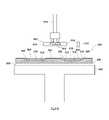
圖8係根據本發明之使用承載帶之方法800的流程圖。圖9係圖8之方法800中之動作的側視截面示意圖。結合參考圖8及圖9,方法800可涉及:回應於對包括凹部302的承載帶300之至少一部分進行加熱,將承載帶300之凹部302自收縮狀態膨脹至膨脹狀態,如動作802所示。例如,可利用熱源加熱承載帶之表面,例如第二主表面306,並且回應於高溫,承載帶300之材料可自收縮狀態膨脹。該膨脹可導致凹部302之側面308或凹部302之突片之間的橫向、縱向或橫向及縱向距離增加至膨脹狀態,以提供用於將半導體晶粒902引入至凹部302中之間隙。8 is a flowchart of a
利用熱源加熱承載帶300或承載帶之一部分可涉及:例如將承載帶300之第二主表面306之一部分支撐在如圖9所示之已加熱卡盤904上。更具體言之,承載帶300之部分可順序地移動穿過已加熱卡盤904之主表面908,從而由加熱卡盤904發出之熱對承載帶300之各別部分進行加熱。作為特定非限制性實例,可自繞有承載帶300之卷軸上拉出承載帶300,以將部分承載帶300送至已加熱卡盤904上方,從而加熱主表面908,使得:當包括一系列各別凹部302的承載帶300之一部分位於已加熱卡盤904上時,該系列各別凹部302自收縮狀態(見圖10)轉變至圖9所示之膨脹狀態。每次可定位在已加熱卡盤904上方並變換為膨脹狀態之凹部302之數量可約為例如2至20個。更具體言之,每次可定位在已加熱卡盤904之主表面908上之凹部302之數量可約為例如3至10個(例如約為5個)。Heating the
當自收縮狀態轉變至膨脹狀態時,承載帶300或承載帶300之一部分可以初始溫度開始並曝露於較高溫度以加熱承載帶300之相關部分。舉例而言,承載帶300最初可處於環境溫度(即室溫)下,且承載帶300之相關部分可曝露於如下所述之溫度:高於室溫且低於可能損壞承載帶300及/或半導體晶粒902之溫度。更具體言之,承載帶300可最初處於約20℃至約25℃之間的溫度,並且承載帶可曝露於約80℃至約120℃ (例如約90℃、約100℃)之間的溫度以將承載帶300之材料變換成膨脹狀態。When transitioning from the contracted state to the expanded state, the
在保持對凹部302進行加熱之時間內,可足以實現自收縮狀態轉變至膨脹狀態以移除半導體晶粒902,以及確保可將任何半導體晶粒902引入處於膨脹狀態之凹部302中以運輸及處置。例如,承載帶300之該部分可保持曝露於高溫不超過60秒。更具體言之,承載帶300之相關部分可保持曝露於高溫約1秒至約30秒(例如約3秒、約5秒)。The time that the
凹部302之側面308之間或相對突片之間的最短距離之變化反映出收縮狀態與膨脹狀態之間的轉變,例如,可為約100微米或更小。更具體言之,凹部302之側面308之間或相對突片之間的距離變化可在約25微米至約75微米之間(例如約50微米)。Changes in the shortest distance between the
一旦給定凹部302已經轉變至膨脹狀態,就可將半導體晶粒902置放在該各別凹部302中,如動作804所示。例如,取置機910可用於將半導體晶粒902自其供應源(例如含有已特性化為已知良好晶粒(KGD)之半導體晶粒902之單粒化晶圓或測試托盤)擷取,並將半導體晶粒902置放在凹部302之已處於膨脹狀態之其中一個凹部中。可重複該過程直至當前處於膨脹狀態之每一凹部302之內部都具有半導體晶粒902。可將半導體晶粒902之主表面908之至少一部分支撐在界定凹部302之底面310上,並且可將界定凹部302之側面308與半導體晶粒902之各別側面914間隔開。在適用的情況下,覆蓋凹部之突片可沿橫向、縱向或橫向及縱向自半導體晶粒902側面914向外定位,並且可將凹部302中之任何凹陷314之底面316與半導體晶粒902之主表面912間隔開。Once a given
在一些實施例中,半導體晶粒902可係薄晶粒。例如,每一半導體晶粒902之厚度916可約為50微米或更小。更具體言之,每一半導體晶粒902之厚度916可在例如約20微米至約50微米之間(例如約30微米)。In some embodiments, semiconductor die 902 may be a thin die. For example, the
圖10係圖8之方法800中之另一動作的側視截面示意圖。結合參考圖8及圖10,凹部302可收縮以回應於對承載帶300之該部分移除熱而將每一半導體晶粒902固定在相關聯之凹部302中,如動作806所示。在一些實施例中,承載帶300可簡單地進給穿過已加熱卡盤904 (見圖9)之主表面908 (見圖9),直至承載帶300之含有已插有半導體晶粒902的凹部302之相關部分位於已加熱卡盤904 (見圖9)之範圍之外,並且可允許承載帶300冷卻至室溫。在其他實施例中,承載帶300之具有處於膨脹狀態之部分凹部302,其中含有半導體晶粒902,可主動冷卻以將該些凹部302收縮至圖10所示之收縮狀態。例如,承載帶300可以自已加熱卡盤904 (見圖9)穿過冷卻卡盤1004之主表面1002之方式進行進給,以主動冷卻承載帶300之相關部分。主動冷卻承載帶300可使凹部302以更快的速率回至收縮狀態,從而:當半導體晶粒902儲存在承載帶300之凹部302中並在卷軸上組裝裝有半導體晶粒之承載帶300時,可有利地增加產量。FIG. 10 is a schematic side cross-sectional view of another act in the
由於承載帶300在熱移除及選用的主動冷卻施加之後冷卻,承載帶300可收縮,使得凹部302自膨脹狀態轉變至收縮狀態。當凹部302處於收縮狀態且半導體晶粒902位於相關聯之凹部302內時,界定凹部302之兩或多個側面308可與各別側面914接觸,或部分突片可覆蓋半導體晶粒902之朝向凹部302外部的上部主表面912之各別部分。例如,界定凹部302之兩個或四個側面308可形成摩擦配合抵靠半導體晶粒902之對應側面914,或部分突片可與自側面914向內定位的主表面912之各別部分接觸。更具體言之,由於界定凹部302之側面308與半導體晶粒902之各別側面914接觸並形成與其抵靠之摩擦配合,因此在半導體晶粒902中引起了最大彎曲應變,其可係例如約0.002 mm/mm (約0.2%)或更小。As the
在實施例中,利用突片412 (見圖4)或突片512 (見圖5)將半導體晶粒902保持在相關聯之凹部302內,給定突片412 (見圖4)或突片512 (見圖5)與半導體晶粒902之主表面912之間具有的最大重疊可係例如約75微米或更小。更具體言之,給定突片412 (見圖4)或突片512 (見圖5)與半導體晶粒902之主表面912之間的最大重疊可在例如約15微米至約50微米之間(例如約25微米)。In an embodiment, the semiconductor die 902 is retained within the associated
雖然已特定地描述上述動作並將其應用於圖3之承載帶300,但亦可將產生半導體晶粒在承載帶300之凹部302內之臨時固定的同樣的膨脹及收縮應用於圖1至圖7中之任何承載帶。Although the above actions have been specifically described and applied to the
綜上所述,在承載帶上儲存微電子裝置之方法可涉及:將承載帶體之一部分自收縮狀態加熱至膨脹狀態,以使承載體中之至少一個凹部在至少一個尺寸維度上膨脹至足以收容微電子裝置。微電子裝置可至少部分地置放在至少一個凹部內。可冷卻(如主動地、被動地)該承載帶體之部分,以使至少一個凹部在該至少一個尺寸維度上收縮並將置放在其中之微電子裝置固定,承載帶體之部分鄰近該凹部。In summary, a method of storing microelectronic devices on a carrier tape may involve heating a portion of the carrier tape body from a contracted state to an expanded state to expand at least one recess in the carrier body sufficiently in at least one dimensional dimension Contains microelectronic devices. The microelectronic device may be placed at least partially within the at least one recess. The portion of the carrier tape may be cooled (eg, actively, passively) to shrink at least one recess in the at least one dimensional dimension and secure the microelectronic device placed therein, the portion of the carrier tape adjacent to the recess .
圖11係用於支撐承載帶100之卷軸1100的透視圖。卷軸1100可包括:例如兩個定向成至少實質上彼此平行之圓盤1104,以及承載帶100可圍繞其纏繞之集線器1106,使得承載帶100之螺旋可圍繞集線器1106位於圓盤1104之間。在一些實施例中,蓋帶1102可置放在凹部102上方,以減少污染或損壞支撐在其中之半導體晶粒902的可能性。例如,蓋帶1102可置放成與承載帶100之至少一部分接觸,以將至少一些半導體晶粒902密封在相關聯之凹部102中。更具體言之,蓋帶1102可沿著承載帶100之長度黏附至第一主表面104以覆蓋每一凹部102並將每一相關聯之半導體晶粒902密封在其各別凹部102內。一旦將蓋帶1102應用至承載帶100上,承載帶100及蓋帶1102可共同地纏繞在卷軸1100上以運輸、儲存、隨後與取置機910 (見圖9)一起使用,或者其任意組合。FIG. 11 is a perspective view of a
在其他實施例中,承載帶100,其凹部102中(例如藉由與側面110接觸或藉由來自突片之機械干涉)支撐有半導體晶粒902,可在不具有任何蓋帶1102的情況下纏繞在卷軸1100上。一旦承載帶100完全纏繞在卷軸1100周圍,則蓋帶1102可僅置放在纏繞在卷軸1100周圍的承載帶100之最外圓周之周圍,或者可圍繞卷軸1100本身置放。例如,蓋帶1102可黏附至承載帶100之第一主表面104上,僅繞卷軸1100旋轉一圈,蓋帶1102可位於卷軸1100自身之圓周周圍,承載帶100位於承載帶100下面,或者蓋帶1102可纏繞在卷軸1100之整個外部,包括形成卷軸1100之圓盤1104及集線器1106之圓周及外表面。與將蓋帶1102應用至承載帶100之第一主表面104之整個長度相比,僅將蓋帶1102纏繞在承載帶100之最外部分之周圍或纏繞在卷軸1100或其部分之周圍可利用較少的資源,且產生較少的浪費。在另一實施方案中,可完全省略蓋帶1102,並且可將配備帶之卷軸1100單獨或與其他承載帶一起置放在密封容器中,以在進一步處置及運輸至目的地期間實現環保,在該目的地處將半導體晶粒移除並在清潔環境中進行處置。In other embodiments,
雖然已特定地描述上述動作並將其應用於圖1之承載帶100,但亦可將圍繞卷軸1100之同樣的臨時定位及由蓋帶1102產生之保護應用至圖1至圖7之任何承載帶中。Although the above actions have been specifically described and applied to the
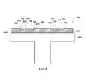
圖12係根據本發明之使用承載帶之方法1200的流程圖。圖13係圖12之方法1200中之動作的側視截面示意圖。結合參考圖12及圖13,方法1200可涉及:回應於對承載帶300之至少一部分進行加熱,將承載帶300之凹部302自收縮狀態膨脹至膨脹狀態,如動作1202所示。亦如動作1202所示,對該部分承載帶300進行加熱可使界定各個凹部302之至少一個表面與位於各個凹部302內之半導體晶粒902脫離接觸。例如,第二主表面306可利用熱源加熱,並且承載帶300之材料回應於利用熱源加熱而自收縮狀態膨脹。該膨脹可導致凹部302之側面308或凹部302之突片之間的橫向、縱向或橫向及縱向距離增加至膨脹狀態,以將半導體晶粒902引入至凹部302中。12 is a flowchart of a
利用熱源加熱承載帶300或承載帶之一部分可涉及:例如將承載帶300之第二主表面306之一部分支撐在已加熱卡盤1302上。更具體言之,承載帶300之部分可順序地移動穿過已加熱卡盤1302之主表面1304 (其可與最初將半導體晶粒902置放在承載帶300中時使用之已加熱卡盤904相同或不同),從而由已加熱卡盤904發出之熱對承載帶300之各別部分進行加熱。作為特定非限制性實例,當承載帶300之部分被拉動並順序地進給至主表面908上方時,承載帶300可自卷軸110展開,同時已加熱卡盤1302對主表面1304進行加熱,使得:當承載帶300之相關部分上之凹部302位於已加熱卡盤1302上時,各別系列之凹部302自收縮狀態(見圖10)轉變至圖13所示之膨脹狀態。每次可以膨脹狀態定位之凹部302之數量可為例如約2至20個。更具體言之,每次可定位在已加熱卡盤1302之主表面1304上之凹部302之數量可約為例如3至10個(例如約為5個)。Heating the
當自收縮狀態轉變至膨脹狀態時,承載帶300或承載帶300之一部分可以初始溫度開始並曝露於較高溫度以加熱承載帶300之相關部分。舉例而言,承載帶300最初可處於環境溫度(即室溫)下,且承載帶300之包括含有半導體晶粒902的凹部302之相關部分可曝露於如下所述之溫度:高於室溫且低於可能損壞承載帶300及/或半導體晶粒902之溫度。更具體言之,承載帶300最初可處於約20℃至約25℃之間,並且承載帶可曝露於約80℃至約120℃之間的溫度(例如,約90℃、約100℃)。When transitioning from the contracted state to the expanded state, the
在保持對相關凹部302進行加熱之時間內,可足以實現自收縮狀態轉變至膨脹狀態,以及確保可將任何半導體晶粒902自處於膨脹狀態之凹部302中移除。例如,承載帶300之該部分可保持曝露於高溫不超過60秒。更具體言之,承載帶300之相關部分可保持曝露於高溫約1秒至約30秒(例如約3秒、約5秒)。The time that the associated
凹部302之側面308之間或相對突片之間的最短距離之變化反映出收縮狀態與膨脹狀態之間的轉變,例如,可為約100微米或更小。更具體言之,凹部302之側面308之間或相對突片之間的距離變化可在約25微米至約75微米之間(例如約50微米)。Changes in the shortest distance between the
一旦給定凹部302已經轉變至膨脹狀態,就可將半導體晶粒902自該各別凹部302中移除,如動作1204所示。例如,取置機1306 (其可係與最初用於將半導體晶粒902置放在凹部302中之取置機910相同或不同的類型)可用於將半導體晶粒902自凹部302之已處於膨脹狀態之其中一個凹部中提起來,可重複該過程直至當前處於膨脹狀態之每一凹部302中沒有任何半導體晶粒902。可將半導體晶粒902之主表面908之至少一部分支撐在界定凹部302之底面310上,並且可將界定凹部302之側面308與各別側面914間隔開。在適用的情況下,覆蓋凹部之突片可沿橫向、縱向或橫向及縱向自半導體晶粒902側面914向外定位,並且可將凹部302中之任何凹陷314之底面316與半導體晶粒902之主表面912間隔開。然後可將半導體晶粒902定位在例如另一組件(例如,晶圓或其他塊體基板、另一半導體晶粒、中介層或PCB)上以將半導體晶粒902電連接至電氣系統(例如記憶體裝置)中之其他組件。Once a given
綜上所述,處置微電子裝置之方法可涉及:回應於加熱包括承載帶之至少一些凹部的承載帶之至少一部分,將該至少一些凹部自收縮狀態膨脹至膨脹狀態,以使承載帶之界定該至少一些凹部中之各別凹部之至少一個表面與位於該至少一些凹部中之各別凹部內之微電子裝置脫離接觸。可將微電子裝置自該至少一些凹部中之各別凹部中移除。In summary, a method of handling a microelectronic device may involve: in response to heating at least a portion of a carrier tape including at least some recesses of the carrier tape, expanding the at least some recesses from a contracted state to an expanded state to define the carrier tape At least one surface of a respective one of the at least some recesses is out of contact with a microelectronic device located within a respective one of the at least some recesses. The microelectronic device can be removed from a respective one of the at least some of the recesses.
根據本發明之承載帶可減少在自承載帶移除期間對半導體晶粒造成損壞的可能性。舉例而言,減少(例如取消)依賴黏附材料將半導體晶粒臨時固定在承載帶之凹部中可減少半導體晶粒上之應力,減少在插入至凹部中並自凹部中移除期間半導體晶粒中同時發生的微裂紋或裂縫之形成及/或傳播。藉由減少在承載帶之整個主表面上配置蓋帶之需要,根據本發明之承載帶亦可利用較少的材料及資源來實現將半導體晶粒臨時儲存在承載帶上以供運輸及處置。承載帶可藉由取消黏附材料進一步降低半導體晶粒之污染可能性。另外,該等承載帶之實施例所揭示之組態可允許每一半導體晶粒關於X及Y方向以及關於垂直軸線之角度(即θ)更精確地定位在凹部中並因此當藉由取置設備之拾取頭移除時便於準確定向,當將半導體晶粒置放在另一組件上時,該設備需要較少的主動補償。換言之,由於若在插入至凹部期間置放不準確,凹部之膨脹及收縮趨於將半導體晶粒對準及重新定位,因此,在自承載帶中移除半導體晶粒期間,承載帶可改良取置過程之精度。The carrier tape according to the present invention can reduce the possibility of damage to the semiconductor die during removal from the carrier tape. For example, reducing (eg eliminating) reliance on adhesive materials to temporarily hold semiconductor dies in recesses of a carrier tape can reduce stress on the semiconductor die, reducing stress on the semiconductor die during insertion into and removal from the recesses Simultaneous formation and/or propagation of microcracks or cracks. By reducing the need to deploy a cover tape over the entire major surface of the carrier tape, the carrier tape according to the present invention can also utilize less material and resources to temporarily store semiconductor dies on the carrier tape for transportation and disposal. The carrier tape can further reduce the possibility of contamination of the semiconductor die by eliminating the adhesive material. In addition, the configurations disclosed in the embodiments of the carrier tapes may allow each semiconductor die to be more precisely positioned in the recesses with respect to the X and Y directions and the angle (ie, θ) with respect to the vertical axis and therefore when placed by The device's pick head is removed to facilitate accurate orientation, and the device requires less active compensation when placing a semiconductor die on another component. In other words, since the expansion and contraction of the recess tends to align and reposition the semiconductor die if placement is inaccurate during insertion into the recess, the carrier tape can be improved during removal of the semiconductor die from the carrier tape. the accuracy of the setting process.
雖然主要係按照包含以下形式之凹部之承載帶進行描述:具有側壁及底面之空腔,但如上所述,承載帶可僅採用以下形式之間隙:完全延伸通過承載帶厚度之狹槽。通常,例如在SURFTAPE®承載帶中,狹槽之底部至少部分地覆蓋有黏附膜,每一狹槽中之半導體晶粒黏附至該黏附膜。然而,本發明之實施例採用具有以下作用之表面之膨脹及收縮:界定各凹部且被組態成在承載帶材料收縮時與半導體晶粒之兩個或多個側邊或側緣接觸,可將每一半導體晶粒固持在適當定位,從而不需要在晶粒下面設置支撐面。詳言之,可修改圖4之設計,將突片412置放在對應於收容在中之晶粒之中間厚度處之水平位置,以牢固地對接並接合晶粒側邊。此外,可修改圖5之設計,在狹槽之具有朝上之斜面之底部包括延伸突片,以夾緊收容在狹槽中之晶粒之側緣。Although primarily described in terms of carrier tapes comprising recesses in the form of cavities with sidewalls and bottom surfaces, as noted above, carrier tapes may only employ gaps in the form of slots extending fully through the thickness of the carrier tape. Typically, such as in SURFTAPE® carrier tapes, the bottoms of the slots are at least partially covered with an adhesive film to which the semiconductor die in each slot is adhered. However, embodiments of the present invention employ expansion and contraction of surfaces that define recesses and are configured to contact two or more sides or edges of the semiconductor die as the carrier tape material shrinks, which may Each semiconductor die is held in place so that no support surface is required under the die. In particular, the design of FIG. 4 can be modified to place the
儘管根據本發明之實施例描述了配備有承載帶之單一卷軸之使用,但經考慮,若藉由卡盤對承載帶進行加熱或冷卻之時間超過使用取置設備置放或拾取半導體晶粒所需之時間,則可採用多個卷軸在共同卡盤上並行地進給承載帶,使得取置設備可與不同承載帶上之多個凹部相互作用,並避免降低產量。類似地,包含用於收容半導體晶粒之凹部之列及行之所謂的「窩伏爾組件(waffle pack)」可根據本發明之實施例來組態,並且與加熱及冷卻卡盤一起使用。此外,可並行地採用多個卷軸,每一卷軸裝載有承載著表現出不同功能之KGD之承載帶,以組裝包含具有不同功能之KGD之總成,例如混合記憶體立方體(HMC),每一混合記憶體立方體(HMC)包含:組態為控制器之邏輯晶粒上之DRAM晶粒堆疊,或高頻寬記憶體(HBM),高頻寬記憶體(HBM)包含在控制器晶粒上之DRAM晶粒堆疊,高頻寬記憶體(HBM)安裝至具有處理器晶粒(例如圖形處理單元(GPU))之共同中介層。在另一實施方案中,本發明之實施例可採用裝在卷軸上之承載帶以接收以特定次序自不同倉拾取的不同類型之半導體晶粒,該特定次序對應於自承載帶擷取半導體晶粒之次序,以與在基底晶圓、中介層、印刷電路板(PCB)或其他組件上之其他組件進行組裝。在此種實施方案中,不同的凹部可具有不同的大小及組態,並可以適當的順序進行製造,以收容不同大小及形狀之不同半導體晶粒。Although the use of a single spool equipped with a carrier tape is described in accordance with embodiments of the present invention, it is contemplated that if the time required to heat or cool the carrier tape by the chuck exceeds the time required to place or pick semiconductor dies using pick and place equipment If desired, multiple spools can be used to feed the carrier tape in parallel on a common chuck, allowing the pick-and-place device to interact with multiple recesses on different carrier tapes and avoid reducing throughput. Similarly, so-called "waffle packs" comprising rows and rows of recesses for housing semiconductor dies may be configured in accordance with embodiments of the present invention and used with heating and cooling chucks. Additionally, multiple reels, each loaded with a carrier tape carrying KGDs exhibiting different functions, can be used in parallel to assemble assemblies containing KGDs having different functions, such as a hybrid memory cube (HMC), each A Hybrid Memory Cube (HMC) consists of a stack of DRAM dies on a logic die configured as a controller, or High Bandwidth Memory (HBM), which consists of a DRAM die on a controller die Stacked, high bandwidth memory (HBM) is mounted to a common interposer with processor dies such as graphics processing units (GPUs). In another implementation, embodiments of the present invention may employ a carrier tape mounted on a spool to receive different types of semiconductor die picked from different bins in a specific order corresponding to picking semiconductor die from the carrier tape order of dies for assembly with other components on a base wafer, interposer, printed circuit board (PCB), or other components. In such an embodiment, the different recesses can have different sizes and configurations, and can be fabricated in an appropriate sequence to accommodate different semiconductor dies of different sizes and shapes.
在本發明之範疇內之另外非限制性實施例包括: 實施例1:一種用於微電子裝置的承載帶,其包含:細長帶體,該細長帶體包含凹部,該等凹部被設定大小、塑形及定位以在各別凹部中收容各別微電子裝置;其中該帶體之材料及該帶體之鄰近該等凹部之部分之組態的熱膨脹係數允許該帶體之該材料回應於該帶體之溫度升高而膨脹,並擴大由該帶體之溫度升高之部分包圍的凹部之至少一個尺寸維度,且允許該凹部收容微電子裝置,並且回應於該部分之溫度自經升高溫度之降低而收縮並使該帶體之鄰近該凹部之至少兩個相對表面與該微電子裝置接觸並固持該微電子裝置。 實施例2:如實施例1之承載帶,其中該帶體之該材料之該熱膨脹係數為3或更大。 實施例3:如實施例1或實施例2之承載帶,其中該帶體在該帶體之鄰近該等凹部之表面上不含黏附材料。 實施例4:如實施例1至3中任一項之承載帶,其中至少一些該等凹部被塑形為使得其隅角部與固持在凹部中之微電子裝置間隔開。 實施例5:如實施例1至4中任一項之承載帶,其中鄰近至少一些該等凹部的該帶體之兩個相對橫向側面被定位成:回應於溫度降低,接觸並固持收容在該至少一些凹部中之微電子裝置。 實施例6:如實施例1至5中任一項之承載帶,其中鄰近至少一些該等凹部的該帶體之兩個橫向側面及兩個縱向側面被定位成:回應於溫度降低,接觸並固持收容在至少一些該等凹部中之微電子裝置。 實施例7:如實施例1至6中任一項之承載帶,其中鄰近至少一些該等凹部之該帶體被組態成使固持在該至少一些該等凹部中之微電子裝置之主表面之至少大部分不與該帶體接觸。 實施例8:如實施例7之承載帶,其中鄰近該至少一些該等凹部之該帶體包含台肩,該台肩圍繞並在該微電子裝置之該主表面之周邊部分下方的周邊之至少一部分及該主表面之其餘部分下方的空間內延伸。 實施例9:如實施例1至8中任一項之承載帶,其中鄰近至少一些該等凹部之該帶體包含接近該至少一些該等凹部之口部之相對突片,該等相對突片被定位成回應於溫度降低而覆蓋收容在該凹部中之微電子裝置之主表面。 實施例10:如實施例9之承載帶,其中每一相對突片被塑形為朝向該凹部之反向倒角。 實施例11:一種在承載帶上儲存微電子裝置之方法,其包含:將承載帶體之一部分自收縮狀態加熱至膨脹狀態,以使承載帶體中之至少一個凹部在至少一個尺寸維度上膨脹至足以收容微電子裝置;將微電子裝置至少部分地置放在該至少一個凹部內;以及冷卻該承載帶體之該部分,以使該至少一個凹部在該至少一個尺寸維度上收縮並將置放在其中之該微電子裝置固定,其中該承載帶體之部分鄰近該凹部。 實施例12:如實施例11之方法,其進一步包含:對該承載帶體之不同的縱向間隔之部分重複該加熱、該置放及該冷卻,同時使該承載帶前進並繞卷軸纏繞該承載帶之固定有微電子裝置之部分。 實施例13:如實施例12之方法,其進一步包含:在繞卷軸纏繞之前,將蓋帶置放在該承載帶之具有微電子裝置之部分中之凹部上方,或者在纏繞之後,將蓋帶繞該承載帶之最外部分置放。 實施例14:如實施例11至13中任一項之方法,其中加熱該承載帶體之至少一部分包含:使該承載帶體之該至少一部分曝露於介於約80℃至約120℃之間的溫度下。 實施例15:如實施例11至14中任一項之方法,其中將微電子裝置置放在該至少一個凹部中包含:置放厚度為約50微米或更小之微電子裝置。 實施例16:如實施例11至15中任一項之方法,其中固定包含:將該微電子裝置之側邊與該承載帶體之鄰近該至少一個凹部之相對表面對接,或者使該承載帶體之相對部分在該微電子裝置之主表面之周邊部分上延伸。 實施例17:如實施例11至16中任一項之方法,其中冷卻該帶體之該部分包含:主動冷卻該承載帶體之該部分。 實施例18:一種處置微電子裝置之方法,其包含:回應於加熱包括承載帶之至少一些凹部的該承載帶之至少一部分,將該至少一些凹部自收縮狀態膨脹至膨脹狀態,以使該承載帶之界定該至少一些凹部中之各別凹部之至少一個表面與位於該至少一些凹部中之該各別凹部內之微電子裝置脫離接觸;以及將該微電子裝置自該至少一些凹部中之該各別凹部中移除。 實施例19:如實施例18之方法,其中加熱該承載帶之該至少一部分包含:將該承載帶之該至少一部分支撐在已加熱卡盤上。 實施例20:如實施例18或實施例19之方法,其中將該微電子裝置自該至少一些凹部中之該各別凹部中移除包含:利用取置設備將該微電子裝置自該至少一些凹部中之該各別凹部中移除。Additional non-limiting examples within the scope of the present invention include: Embodiment 1: A carrier tape for a microelectronic device comprising: an elongated tape body including recesses sized, shaped and positioned to receive respective microelectronics in respective recesses A device; wherein the thermal expansion coefficients of the material of the belt and the configuration of the portion of the belt adjacent the recesses allow the material of the belt to expand in response to an increase in the temperature of the belt, and to expand from the belt at least one dimensional dimension of the recess surrounded by the elevated temperature portion and allowing the recess to house a microelectronic device and shrink in response to the temperature of the portion decreasing from the elevated temperature At least two opposing surfaces contact and hold the microelectronic device. Embodiment 2: The carrier tape of Embodiment 1, wherein the thermal expansion coefficient of the material of the tape body is 3 or more. Embodiment 3: The carrier tape of Embodiment 1 or Embodiment 2, wherein the tape body does not contain adhesive material on the surface of the tape body adjacent to the recesses. Embodiment 4: The carrier tape of any one of Embodiments 1-3, wherein at least some of the recesses are shaped such that their corners are spaced apart from the microelectronic devices held in the recesses. Embodiment 5: The carrier tape of any one of Embodiments 1 to 4, wherein two opposite lateral sides of the tape body adjacent at least some of the recesses are positioned to contact and retain the tape body in response to a decrease in temperature. Microelectronic devices in at least some of the recesses. Embodiment 6: The carrier tape of any one of Embodiments 1 to 5, wherein two lateral sides and two longitudinal sides of the tape body adjacent at least some of the recesses are positioned to contact and Microelectronic devices housed in at least some of the recesses are retained. Embodiment 7: The carrier tape of any one of Embodiments 1-6, wherein the tape body adjacent to at least some of the recesses is configured to retain a major surface of a microelectronic device in the at least some of the recesses At least most of them are not in contact with the belt body. Embodiment 8: The carrier tape of Embodiment 7, wherein the tape body adjacent to the at least some of the recesses includes a shoulder surrounding at least one of the perimeters of and below the perimeter portion of the major surface of the microelectronic device A portion and the remainder of the main surface extend in the space below. Embodiment 9: The carrier tape of any one of Embodiments 1 to 8, wherein the tape body adjacent to at least some of the recesses includes opposing tabs adjacent to the mouth of the at least some of the recesses, the opposing tabs is positioned to cover a major surface of a microelectronic device housed in the recess in response to a decrease in temperature. Embodiment 10: The carrier tape of Embodiment 9, wherein each opposing tab is shaped as a reverse chamfer toward the recess. Embodiment 11: A method of storing microelectronic devices on a carrier tape, comprising: heating a portion of a carrier tape body from a contracted state to an expanded state to expand at least one recess in the carrier tape body in at least one dimensional dimension enough to accommodate a microelectronic device; placing the microelectronic device at least partially within the at least one recess; and cooling the portion of the carrier tape such that the at least one recess shrinks in the at least one dimensional dimension and places the The microelectronic device placed therein is fixed, wherein a portion of the carrier tape is adjacent to the concave portion. Embodiment 12: The method of Embodiment 11, further comprising: repeating the heating, the placing, and the cooling for different longitudinally spaced portions of the carrier tape body while advancing the carrier tape and wrapping the carrier around a reel The portion of the belt that holds the microelectronic device. Embodiment 13: The method of Embodiment 12, further comprising: placing a cover tape over a recess in the portion of the carrier tape having the microelectronic device prior to winding around the reel, or after wrapping the cover tape Placed around the outermost portion of the carrier tape. Embodiment 14: The method of any one of Embodiments 11-13, wherein heating at least a portion of the carrier tape comprises: exposing the at least a portion of the carrier tape to between about 80°C and about 120°C at the temperature. Embodiment 15: The method of any one of Embodiments 11-14, wherein placing a microelectronic device in the at least one recess comprises: placing a microelectronic device having a thickness of about 50 microns or less. Embodiment 16: The method of any one of Embodiments 11 to 15, wherein fixing comprises: abutting a side of the microelectronic device with an opposite surface of the carrier tape body adjacent to the at least one recess, or making the carrier tape An opposing portion of the body extends over a peripheral portion of the major surface of the microelectronic device. Embodiment 17: The method of any one of Embodiments 11 to 16, wherein cooling the portion of the tape comprises: actively cooling the portion of the carrier tape. Embodiment 18: A method of handling a microelectronic device comprising: in response to heating at least a portion of the carrier tape including at least some recesses of the carrier tape, expanding the at least some recesses from a contracted state to an expanded state to cause the carrier tape at least one surface of the strip defining a respective one of the at least some recesses is out of contact with a microelectronic device located within the respective one of the at least some recesses; and removing the microelectronic device from the one of the at least some recesses removed from the respective recesses. Embodiment 19: The method of Embodiment 18, wherein heating the at least a portion of the carrier tape comprises: supporting the at least a portion of the carrier tape on a heated chuck. Embodiment 20: The method of embodiment 18 or embodiment 19, wherein removing the microelectronic device from the respective one of the at least some of the recesses comprises: utilizing a pick-and-place device to remove the microelectronic device from the at least some of the recesses The respective ones of the recesses are removed.
雖然已經結合各圖描述了某些說明性實施例,但一般熟習此項技術者將認識及理解,本發明之範疇不限於在本發明中明確展示及描述之實施例。相反地,可對本發明中所描述之實施例作許多添加、刪除及修改以產生在本發明之範疇內之實施例,例如明確主張之實施例,包括法律等效物。此外,來自一個所揭示實施例之特徵可與另一所揭示實施例之特徵組合,但仍在本發明之範疇內。While certain illustrative embodiments have been described in connection with the various figures, those of ordinary skill in the art will recognize and understand that the scope of the present invention is not limited to the embodiments expressly shown and described in the present invention. Rather, many additions, deletions, and modifications to the embodiments described in this disclosure can be made to produce embodiments within the scope of the disclosure, such as those expressly claimed, including legal equivalents. Furthermore, features from one disclosed embodiment may be combined with features of another disclosed embodiment while remaining within the scope of the invention.
100:承載帶 102:凹部 104:第一主表面 106:第二主表面 108:底面 110:側面 200:承載帶 202:凹部 204:第一主表面 206:第二主表面 208:缺口 300:承載帶 302:凹部 304:第一主表面 306:第二主表面 308:側面 310:底面 312:台肩 314:凹陷 316:底面 400:承載帶 402:凹部 404:第一主表面 406:第二主表面 408:側面 412:突片 414:第一寬度 416:第二寬度 418:遠端 500:承載帶 502:凹部 504:第一主表面 506:第二主表面 508:側面 510:底面 512:突片 514:表面 516:第一寬度 600:承載帶 602:凹部 604:第一主表面 606:隅角部 608:第三寬度 610:第一長度 612:橫向側面 614:縱向側面 616:第四寬度 618:第二長度 700:承載帶 702:凹部 704:第一主表面 706:隅角部 710:橫向側面 712:縱向側面 800:方法 802:動作 804:動作 806:動作 902:半導體晶粒 904:卡盤 908:主表面 910:取置機 912:主表面 914:側面 916:厚度 1002:主表面 1004:冷卻卡盤 1100:卷軸 1102:蓋帶 1104:圓盤 1106:集線器 1200:方法 1202:動作 1204:動作 1302:卡盤 1304:主表面 1306:取置機100: Carrier belt 102: Recess 104: First main surface 106: Second main surface 108: Underside 110: Side 200: Carrier belt 202: Recess 204: First main surface 206: Second main surface 208: Notch 300: Carrier belt 302: Recess 304: First main surface 306: Second main surface 308: Side 310: Underside 312: Shoulder 314: Sag 316: Underside 400: Carrier belt 402: Recess 404: First major surface 406: Second main surface 408: Side 412: Tabs 414: first width 416: second width 418: Remote 500: Carrier belt 502: Recess 504: First main surface 506: Second main surface 508: Side 510: Bottom 512: Tabs 514: Surface 516:First width 600: Carrier belt 602: Recess 604: First main surface 606: Corner 608: Third width 610: First length 612: Lateral side 614: Longitudinal side 616: Fourth width 618: second length 700: Carrier belt 702: Recess 704: First main surface 706: Corner 710: Lateral side 712: Longitudinal side 800: Method 802: Action 804: Action 806: Action 902: Semiconductor Die 904: Chuck 908: Main Surface 910: Pick-and-place machine 912: Main Surface 914: Side 916: Thickness 1002: Main Surface 1004: Cooling Chuck 1100: Scroll 1102: Cover Tape 1104: Disc 1106: Hub 1200: Method 1202: Action 1204: Action 1302: Chuck 1304: Main Surface 1306: Pick-and-place machine
雖然本發明以特別指出並明確主張特定實施例之申請專利範圍作為結尾,但當結合隨附圖式閱讀時,根據以下描述,可更容易地確定本發明之範疇內之實施例之各種特徵及優點。在圖式中: 圖1係根據本發明之承載帶之一部分的截面側視圖; 圖2係承載帶之另一實施例之一部分的截面側視圖; 圖3係承載帶之另一實施例之一部分的截面側視圖; 圖4係承載帶之另一實施例之一部分的截面側視圖; 圖5係承載帶之另一實施例之一部分的截面側視圖; 圖6係根據本發明之承載帶之一部分的頂面視圖; 圖7係承載帶之另一實施例之一部分的頂面視圖; 圖8係根據本發明之使用承載帶之方法的流程圖; 圖9係圖8之方法中之動作的側視截面示意圖; 圖10係圖8之方法中之另一動作的側視截面示意圖; 圖11係用於支撐承載帶之卷軸的透視圖; 圖12係根據本發明之使用承載帶之方法的流程圖;以及 圖13係圖12之方法中之動作的側視截面示意圖。While the disclosure concludes with the scope of the claims for particular embodiments particularly pointed out and distinctly claimed, the various features of the embodiments within the scope of the disclosure and the following description can be more readily ascertained when read in conjunction with the accompanying drawings advantage. In the schema: Figure 1 is a cross-sectional side view of a portion of a carrier tape according to the present invention; Figure 2 is a cross-sectional side view of a portion of another embodiment of a carrier tape; Figure 3 is a cross-sectional side view of a portion of another embodiment of the carrier tape; 4 is a cross-sectional side view of a portion of another embodiment of a carrier tape; Figure 5 is a cross-sectional side view of a portion of another embodiment of a carrier tape; Figure 6 is a top view of a portion of a carrier tape according to the present invention; Figure 7 is a top view of a portion of another embodiment of the carrier tape; 8 is a flow chart of a method of using a carrier tape according to the present invention; 9 is a schematic side cross-sectional view of an action in the method of FIG. 8; 10 is a schematic side cross-sectional view of another act in the method of FIG. 8; Figure 11 is a perspective view of a reel for supporting the carrier tape; 12 is a flow chart of a method of using a carrier tape according to the present invention; and FIG. 13 is a schematic side cross-sectional view of an act in the method of FIG. 12 .
100:承載帶100: Carrier belt
104:第一主表面104: First main surface
902:半導體晶粒902: Semiconductor Die
1100:卷軸1100: Scroll
1102:蓋帶1102: Cover Tape
1104:圓盤1104: Disc
1106:集線器1106: Hub
Claims (20)
Translated fromChineseApplications Claiming Priority (2)
| Application Number | Priority Date | Filing Date | Title |
|---|---|---|---|
| US202063119946P | 2020-12-01 | 2020-12-01 | |
| US63/119,946 | 2020-12-01 |
Publications (1)
| Publication Number | Publication Date |
|---|---|
| TW202222656Atrue TW202222656A (en) | 2022-06-16 |
Family
ID=81770319
Family Applications (1)
| Application Number | Title | Priority Date | Filing Date |
|---|---|---|---|
| TW110114374ATW202222656A (en) | 2020-12-01 | 2021-04-21 | Carrier tapes for microelectronic devices and related methods |
Country Status (2)
| Country | Link |
|---|---|
| CN (1) | CN114582775A (en) |
| TW (1) | TW202222656A (en) |
Family Cites Families (12)
| Publication number | Priority date | Publication date | Assignee | Title |
|---|---|---|---|---|
| CA1322271C (en)* | 1987-02-25 | 1993-09-21 | Sho Masujima | Carrier tape for electronic circuit elements and method of manufacturing an electronic circuit element series |
| JPH09169386A (en)* | 1995-12-20 | 1997-06-30 | Hitachi Ltd | Carrier tape and method for manufacturing the same |
| JP3678561B2 (en)* | 1997-10-13 | 2005-08-03 | 株式会社リコー | Thermal expansion / contraction carrier tape and taping method |
| US6469372B2 (en)* | 2000-05-16 | 2002-10-22 | Texas Instruments Incorporated | Matched thermal expansion carrier tape assemblage for semiconductor devices |
| JP4722415B2 (en)* | 2004-06-14 | 2011-07-13 | 三菱電機株式会社 | Semiconductor device and manufacturing method thereof |
| US20060157381A1 (en)* | 2005-01-20 | 2006-07-20 | Adams James T | Component carrier and method for making |
| US7985621B2 (en)* | 2006-08-31 | 2011-07-26 | Ati Technologies Ulc | Method and apparatus for making semiconductor packages |
| US9869392B2 (en)* | 2011-10-20 | 2018-01-16 | Lam Research Corporation | Edge seal for lower electrode assembly |
| JP5891133B2 (en)* | 2012-07-12 | 2016-03-22 | スタンレー電気株式会社 | Semiconductor light emitting device |
| US20180286733A1 (en)* | 2017-03-30 | 2018-10-04 | Intel Corporation | Die carrier device and method |
| US10153195B1 (en)* | 2017-05-18 | 2018-12-11 | Micron Technology, Inc. | Semiconductor constructions comprising dielectric material |
| EP3765653A1 (en)* | 2018-03-13 | 2021-01-20 | View, Inc. | Carrier with vertical grid for supporting substrates in coater |
- 2021
- 2021-04-21TWTW110114374Apatent/TW202222656A/enunknown
- 2021-05-12CNCN202110517579.9Apatent/CN114582775A/enactivePending
Also Published As
| Publication number | Publication date |
|---|---|
| CN114582775A (en) | 2022-06-03 |
Similar Documents
| Publication | Publication Date | Title |
|---|---|---|
| TWI356798B (en) | Packing structure for semiconductor device, packin | |
| JP6395972B1 (en) | Carrier tape | |
| US11764133B2 (en) | Tape carrier assemblies having an integrated adhesive film | |
| JP2003312726A (en) | Carrier tape and storage device for storing small articles | |
| TW201637115A (en) | Carrier tape and carrier tape assembly | |
| CN112744453A (en) | Carrier tape system for semiconductor device | |
| TW202222656A (en) | Carrier tapes for microelectronic devices and related methods | |
| US20030218236A1 (en) | Chip carrier tape | |
| US7061108B2 (en) | Semiconductor device and a method for securing the device in a carrier tape | |
| JP2006100297A (en) | Method for transporting semiconductor device and method for manufacturing semiconductor device | |
| JP4755410B2 (en) | Tape-shaped component packaging | |
| TWI680925B (en) | Semiconductor chip holder and packaging method | |
| JP5505658B2 (en) | Electronic device manufacturing method, electronic component mounting frame, electronic component stored in mounting frame, and surface mounting device | |
| JP4475888B2 (en) | Carrier tape for transporting electronic components | |
| TW201710160A (en) | Carrier tape of electronic component and method of packaging electronic component using the same | |
| US20200118940A1 (en) | Die with bumper for solder joint reliability | |
| ES2299607T3 (en) | PACK FOR A MAGNETIC TAPE REEL. | |
| JPH0226872Y2 (en) | ||
| JP2007161278A (en) | Pallet, optical component manufacturing method using the pallet, optical component packaging body and container | |
| JPS61152514A (en) | Method of packaging semiconductor pellet | |
| JPH0551764U (en) | Embossed carrier tape | |
| CN115954305A (en) | Wafer storage device and wafer taking and placing method | |
| JP2002009107A (en) | Jig for correcting deformation produced in semiconductor carrier tape | |
| JP5457686B2 (en) | Method for preventing deformation of a take-up reel for electronic components | |
| JPH09315488A (en) | Electronic parts carrying body |