TW202215108A - Optical system - Google Patents
Optical systemDownload PDFInfo
- Publication number
- TW202215108A TW202215108ATW110131127ATW110131127ATW202215108ATW 202215108 ATW202215108 ATW 202215108ATW 110131127 ATW110131127 ATW 110131127ATW 110131127 ATW110131127 ATW 110131127ATW 202215108 ATW202215108 ATW 202215108A
- Authority
- TW
- Taiwan
- Prior art keywords
- region
- coupling
- partially reflective
- loe
- reflective surfaces
- Prior art date
Links
Images


Classifications
- G—PHYSICS
- G02—OPTICS
- G02B—OPTICAL ELEMENTS, SYSTEMS OR APPARATUS
- G02B27/00—Optical systems or apparatus not provided for by any of the groups G02B1/00 - G02B26/00, G02B30/00
- G02B27/0081—Optical systems or apparatus not provided for by any of the groups G02B1/00 - G02B26/00, G02B30/00 with means for altering, e.g. enlarging, the entrance or exit pupil
- B—PERFORMING OPERATIONS; TRANSPORTING
- B29—WORKING OF PLASTICS; WORKING OF SUBSTANCES IN A PLASTIC STATE IN GENERAL
- B29D—PRODUCING PARTICULAR ARTICLES FROM PLASTICS OR FROM SUBSTANCES IN A PLASTIC STATE
- B29D11/00—Producing optical elements, e.g. lenses or prisms
- B29D11/00663—Production of light guides
- G—PHYSICS
- G02—OPTICS
- G02B—OPTICAL ELEMENTS, SYSTEMS OR APPARATUS
- G02B27/00—Optical systems or apparatus not provided for by any of the groups G02B1/00 - G02B26/00, G02B30/00
- G—PHYSICS
- G02—OPTICS
- G02B—OPTICAL ELEMENTS, SYSTEMS OR APPARATUS
- G02B27/00—Optical systems or apparatus not provided for by any of the groups G02B1/00 - G02B26/00, G02B30/00
- G02B27/0018—Optical systems or apparatus not provided for by any of the groups G02B1/00 - G02B26/00, G02B30/00 with means for preventing ghost images
- G—PHYSICS
- G02—OPTICS
- G02B—OPTICAL ELEMENTS, SYSTEMS OR APPARATUS
- G02B27/00—Optical systems or apparatus not provided for by any of the groups G02B1/00 - G02B26/00, G02B30/00
- G02B27/01—Head-up displays
- G—PHYSICS
- G02—OPTICS
- G02B—OPTICAL ELEMENTS, SYSTEMS OR APPARATUS
- G02B27/00—Optical systems or apparatus not provided for by any of the groups G02B1/00 - G02B26/00, G02B30/00
- G02B27/01—Head-up displays
- G02B27/017—Head mounted
- G02B27/0172—Head mounted characterised by optical features
- G—PHYSICS
- G02—OPTICS
- G02B—OPTICAL ELEMENTS, SYSTEMS OR APPARATUS
- G02B27/00—Optical systems or apparatus not provided for by any of the groups G02B1/00 - G02B26/00, G02B30/00
- G02B27/10—Beam splitting or combining systems
- G—PHYSICS
- G02—OPTICS
- G02B—OPTICAL ELEMENTS, SYSTEMS OR APPARATUS
- G02B27/00—Optical systems or apparatus not provided for by any of the groups G02B1/00 - G02B26/00, G02B30/00
- G02B27/10—Beam splitting or combining systems
- G02B27/14—Beam splitting or combining systems operating by reflection only
- G02B27/143—Beam splitting or combining systems operating by reflection only using macroscopically faceted or segmented reflective surfaces
- G—PHYSICS
- G02—OPTICS
- G02B—OPTICAL ELEMENTS, SYSTEMS OR APPARATUS
- G02B27/00—Optical systems or apparatus not provided for by any of the groups G02B1/00 - G02B26/00, G02B30/00
- G02B27/10—Beam splitting or combining systems
- G02B27/14—Beam splitting or combining systems operating by reflection only
- G02B27/145—Beam splitting or combining systems operating by reflection only having sequential partially reflecting surfaces
- G—PHYSICS
- G02—OPTICS
- G02B—OPTICAL ELEMENTS, SYSTEMS OR APPARATUS
- G02B6/00—Light guides; Structural details of arrangements comprising light guides and other optical elements, e.g. couplings
- G—PHYSICS
- G02—OPTICS
- G02B—OPTICAL ELEMENTS, SYSTEMS OR APPARATUS
- G02B6/00—Light guides; Structural details of arrangements comprising light guides and other optical elements, e.g. couplings
- G02B6/0001—Light guides; Structural details of arrangements comprising light guides and other optical elements, e.g. couplings specially adapted for lighting devices or systems
- G02B6/0011—Light guides; Structural details of arrangements comprising light guides and other optical elements, e.g. couplings specially adapted for lighting devices or systems the light guides being planar or of plate-like form
- G02B6/0013—Means for improving the coupling-in of light from the light source into the light guide
- G02B6/0023—Means for improving the coupling-in of light from the light source into the light guide provided by one optical element, or plurality thereof, placed between the light guide and the light source, or around the light source
- G02B6/0031—Reflecting element, sheet or layer
- G—PHYSICS
- G02—OPTICS
- G02B—OPTICAL ELEMENTS, SYSTEMS OR APPARATUS
- G02B6/00—Light guides; Structural details of arrangements comprising light guides and other optical elements, e.g. couplings
- G02B6/0001—Light guides; Structural details of arrangements comprising light guides and other optical elements, e.g. couplings specially adapted for lighting devices or systems
- G02B6/0011—Light guides; Structural details of arrangements comprising light guides and other optical elements, e.g. couplings specially adapted for lighting devices or systems the light guides being planar or of plate-like form
- G02B6/0033—Means for improving the coupling-out of light from the light guide
- G02B6/005—Means for improving the coupling-out of light from the light guide provided by one optical element, or plurality thereof, placed on the light output side of the light guide
- G02B6/0055—Reflecting element, sheet or layer
- G—PHYSICS
- G02—OPTICS
- G02B—OPTICAL ELEMENTS, SYSTEMS OR APPARATUS
- G02B6/00—Light guides; Structural details of arrangements comprising light guides and other optical elements, e.g. couplings
- G02B6/24—Coupling light guides
- G02B6/26—Optical coupling means
- G—PHYSICS
- G03—PHOTOGRAPHY; CINEMATOGRAPHY; ANALOGOUS TECHNIQUES USING WAVES OTHER THAN OPTICAL WAVES; ELECTROGRAPHY; HOLOGRAPHY
- G03B—APPARATUS OR ARRANGEMENTS FOR TAKING PHOTOGRAPHS OR FOR PROJECTING OR VIEWING THEM; APPARATUS OR ARRANGEMENTS EMPLOYING ANALOGOUS TECHNIQUES USING WAVES OTHER THAN OPTICAL WAVES; ACCESSORIES THEREFOR
- G03B21/00—Projectors or projection-type viewers; Accessories therefor
- G03B21/005—Projectors using an electronic spatial light modulator but not peculiar thereto
- G03B21/006—Projectors using an electronic spatial light modulator but not peculiar thereto using LCD's
- G—PHYSICS
- G03—PHOTOGRAPHY; CINEMATOGRAPHY; ANALOGOUS TECHNIQUES USING WAVES OTHER THAN OPTICAL WAVES; ELECTROGRAPHY; HOLOGRAPHY
- G03B—APPARATUS OR ARRANGEMENTS FOR TAKING PHOTOGRAPHS OR FOR PROJECTING OR VIEWING THEM; APPARATUS OR ARRANGEMENTS EMPLOYING ANALOGOUS TECHNIQUES USING WAVES OTHER THAN OPTICAL WAVES; ACCESSORIES THEREFOR
- G03B21/00—Projectors or projection-type viewers; Accessories therefor
- G03B21/14—Details
- G03B21/142—Adjusting of projection optics
- G—PHYSICS
- G03—PHOTOGRAPHY; CINEMATOGRAPHY; ANALOGOUS TECHNIQUES USING WAVES OTHER THAN OPTICAL WAVES; ELECTROGRAPHY; HOLOGRAPHY
- G03B—APPARATUS OR ARRANGEMENTS FOR TAKING PHOTOGRAPHS OR FOR PROJECTING OR VIEWING THEM; APPARATUS OR ARRANGEMENTS EMPLOYING ANALOGOUS TECHNIQUES USING WAVES OTHER THAN OPTICAL WAVES; ACCESSORIES THEREFOR
- G03B33/00—Colour photography, other than mere exposure or projection of a colour film
- G03B33/10—Simultaneous recording or projection
- G03B33/12—Simultaneous recording or projection using beam-splitting or beam-combining systems, e.g. dichroic mirrors
- G—PHYSICS
- G02—OPTICS
- G02B—OPTICAL ELEMENTS, SYSTEMS OR APPARATUS
- G02B27/00—Optical systems or apparatus not provided for by any of the groups G02B1/00 - G02B26/00, G02B30/00
- G02B27/01—Head-up displays
- G02B27/0101—Head-up displays characterised by optical features
- G02B2027/0123—Head-up displays characterised by optical features comprising devices increasing the field of view
- G—PHYSICS
- G02—OPTICS
- G02B—OPTICAL ELEMENTS, SYSTEMS OR APPARATUS
- G02B27/00—Optical systems or apparatus not provided for by any of the groups G02B1/00 - G02B26/00, G02B30/00
- G02B27/01—Head-up displays
- G02B27/0101—Head-up displays characterised by optical features
- G02B2027/013—Head-up displays characterised by optical features comprising a combiner of particular shape, e.g. curvature
- G—PHYSICS
- G02—OPTICS
- G02B—OPTICAL ELEMENTS, SYSTEMS OR APPARATUS
- G02B27/00—Optical systems or apparatus not provided for by any of the groups G02B1/00 - G02B26/00, G02B30/00
- G02B27/01—Head-up displays
- G02B27/0149—Head-up displays characterised by mechanical features
- G02B2027/015—Head-up displays characterised by mechanical features involving arrangement aiming to get less bulky devices
- G—PHYSICS
- G02—OPTICS
- G02B—OPTICAL ELEMENTS, SYSTEMS OR APPARATUS
- G02B27/00—Optical systems or apparatus not provided for by any of the groups G02B1/00 - G02B26/00, G02B30/00
- G02B27/01—Head-up displays
- G02B27/0189—Sight systems
Landscapes
- Physics & Mathematics (AREA)
- General Physics & Mathematics (AREA)
- Optics & Photonics (AREA)
- Engineering & Computer Science (AREA)
- Health & Medical Sciences (AREA)
- Manufacturing & Machinery (AREA)
- Ophthalmology & Optometry (AREA)
- Mechanical Engineering (AREA)
- Optical Elements Other Than Lenses (AREA)
- Optical Integrated Circuits (AREA)
Abstract
Description
Translated fromChinese本發明涉及光學系統,並且特別地涉及用於對來自圖像投影儀的圖像進行二維擴展以顯示給使用者的光學系統。The present invention relates to optical systems, and in particular to optical systems for two-dimensional expansion of an image from an image projector for display to a user.
在圖1A中示出了近眼顯示光學引擎,其包括圖像投影儀200,該圖像投影儀通過透射小平面部(耦合稜鏡)202T以及通過豎直孔徑203V將具有角度場的圖像光投射到波導204中。光在波導中傳播,通過全內反射被反射。嵌入波導中的部分反射器206將圖像從波導朝向具有眼球中心208的觀察者反射出去(虛線箭頭)。A near-eye display optical engine is shown in FIG. 1A, which includes an
圖1B示出了通過使用在其背側具有鏡的反射耦合稜鏡202R耦合到波導中的替選方式。FIG. 1B shows an alternative way of coupling into a waveguide by using a
圖1C示意性地示出了2D孔徑擴展波導的正視圖。此處,圖像投影儀200通過耦合稜鏡202使圖像穿過橫向孔徑203L(203V也存在,但從該取向不可見)射入到波導204中。當圖像光線220A被波導面之間的全內反射(total-internal-reflection,TIR)反射時,圖像光線在波導中橫向傳播。此處使用兩組小平面:組206L通過將所引導的圖像逐漸地反射到不同的引導方向220B來橫向地擴展孔徑,而小平面組206V通過將圖像從波導上的區域210逐漸地耦出到觀察者的眼睛上來豎直地擴展孔徑。Figure 1C schematically shows a front view of a 2D aperture expansion waveguide. Here, the
本發明是一種用於將在耦入區域處射入的圖像照射引導至眼動箱以供使用者觀看的光學系統。The present invention is an optical system for directing image illumination incident at a coupling region to an eye-tracking box for viewing by a user.
根據本發明的實施方式的教導,提供了一種用於將在耦入區域處射入的圖像照射引導至眼動箱以供使用者的眼睛觀看的光學系統,該光學系統包括由透明材料形成的光導光學元件(light-guide optical element,LOE),該LOE包括:(a)第一區域,其包含具有第一取向的平面的、相互平行的第一組部分反射表面;(b)第二區域,其包含具有第二取向的平面的、相互平行的第二組部分反射表面,第二取向不平行於第一取向;(c)一組相互平行的主外表面,主外表面跨第一區域和第二區域延伸,使得第一組部分反射表面和第二組部分反射表面二者位於主外表面之間,其中,第二組部分反射表面與主外表面成斜角,使得通過主外表面處的內反射在LOE內從第一區域傳播到第二區域中的圖像照射的一部分從LOE朝向眼動箱耦出,並且其中,第一組部分反射表面被定向成使得來自耦入區域的、通過主外表面處的內反射在LOE內傳播的圖像照射的一部分朝向第二區域偏轉,其中,第一組部分反射表面包括:第一部分反射表面,其靠近耦入區域,以貢獻於使用者在眼動箱處觀看到的視場的第一部分;第三部分反射表面,其在耦入區域遠側,以貢獻於用戶在眼動箱處觀看到的視場的第三部分;以及第二部分反射表面,其位於第一部分反射表面與第三部分反射表面之間的中間平面中,以貢獻於用戶在眼動箱處觀看到的視場的第二部分,其中,第二部分反射表面被部署在中間平面的子區域中,使得從耦入區域傳播到第三部分反射表面、並且貢獻於用戶在眼動箱處觀看到的視場的第三部分的圖像照射穿過中間平面,而不穿過第二部分反射表面。In accordance with the teachings of embodiments of the present invention, there is provided an optical system for directing image illumination incident at a coupling-in region to an eye-tracking box for viewing by a user's eyes, the optical system comprising being formed from a transparent material The light-guide optical element (LOE) ofThe LOE includes: (a) a first region comprising a first set of mutually parallel partially reflective surfaces having planes having a first orientation; (b) a second region comprising flat surfaces having a second orientation parallel to each other (c) a set of mutually parallel major outer surfaces extending across the first and second regions such that the first set of partially reflective surfaces and a second set of partially reflective surfaces located between the primary outer surfaces, wherein the second set of partially reflective surfaces is at an oblique angle to the primary outer surface such that internal reflections at the primary outer surface propagate from the first region to the primary outer surface within the LOE. A portion of the image illumination in the second region is coupled out of the LOE towards the eye-tracking box, and wherein the first set of partially reflective surfaces is oriented such that internal reflections from the coupled-in region propagate within the LOE through internal reflections at the main outer surface A portion of the image illumination is deflected towards the second region, wherein the first set of partially reflective surfaces includes a first partially reflective surface proximate the coupling-in region to contribute to the first portion of the field of view viewed by the user at the eye box a portion; a third partially reflective surface distal to the coupling region to contribute to a third portion of the field of view viewed by the user at the eyebox; and a second partially reflective surface located between the first partially reflective surface and the first partially reflective surface in the mid-plane between the three partially reflective surfaces to contribute to the second portion of the field of view viewed by the user at the eyebox, wherein the second partially reflective surface is deployed in a sub-region of the mid-plane so that the The incoming region propagates to the third partially reflective surface and contributes to the image of the third portion of the field of view viewed by the user at the eye box illuminated through the mid-plane and not through the second partially reflective surface.
根據本發明的實施方式的另一特徵,耦入區域包括耦入稜鏡,該耦入稜鏡具有作為第一區域中的主外表面之一的延續的第一平面表面,耦入稜鏡具有垂直於主外表面測量的、大於LOE的厚度的厚度尺寸。According to another feature of an embodiment of the present invention, the coupling region includes a coupling region having a first planar surface that is a continuation of one of the major outer surfaces in the first region, the coupling region having Thickness dimension greater than the thickness of the LOE measured perpendicular to the major outer surface.
根據本發明的實施方式的另一特徵,耦入稜鏡呈現耦入表面和耦入稜鏡之間的過渡線作為LOE,耦入表面在平行於主外表面的維度上限定耦入稜鏡的光學孔徑,並且過渡線在垂直於主外表面的維度上限定耦入稜鏡的光學孔徑。According to another feature of an embodiment of the present invention, the coupling surface defines as LOE a transition line between the coupling surface and the coupling surface defining the incoupling surface in a dimension parallel to the main outer surface. an optical aperture, and the transition line defines the optical aperture of the coupling-in aperture in a dimension normal to the major outer surface.
根據本發明的實施方式的另一特徵,第一組部分反射表面還包括位於耦入稜鏡的體積內的至少一個部分反射表面。According to another feature of an embodiment of the invention, the first set of partially reflective surfaces further includes at least one partially reflective surface located within the volume coupled into the cavity.
根據本發明的實施方式的教導,還提供了一種用於將在耦入區域處射入的圖像照射引導至眼動箱以供使用者的眼睛觀看的光學系統,該光學系統包括由透明材料形成的光導光學元件(LOE),該LOE包括:(a)第一區域,其包含具有第一取向的平面的、相互平行的第一組部分反射表面;(b)第二區域,其包含具有第二取向的平面的、相互平行的第二組部分反射表面,第二取向不平行於第一取向;(c)一組相互平行的主外表面,主外表面跨第一區域和第二區域延伸,使得第一組部分反射表面和第二組部分反射表面二者位於主外表面之間,其中,第二組部分反射表面與主外表面成斜角,使得通過主外表面處的內反射在LOE內從第一區域傳播到第二區域中的圖像照射的一部分從LOE朝向眼動箱耦出,並且其中,第一組部分反射表面被定向成使得來自耦入區域的、通過主外表面處的內反射在LOE內傳播的圖像照射的一部分朝向第二區域偏轉,其中,耦入區域包括耦入稜鏡,該耦入稜鏡具有作為第一區域中的主外表面之一的延續的第一平面表面,耦入稜鏡具有垂直於主外表面測量的、大於LOE的厚度的厚度尺寸,並且其中,耦入稜鏡呈現耦入表面和耦入稜鏡之間的過渡線作為LOE,耦入表面在平行於主外表面的維度上限定耦入稜鏡的光學孔徑,並且過渡線在垂直於主外表面的維度上限定耦入稜鏡的光學孔徑。In accordance with the teachings of embodiments of the present invention, there is also provided an optical system for directing image illumination incident at a coupling-in region to an eye-tracking box for viewing by a user's eyes, the optical system comprising a transparent material A formed light guide optical element (LOE) comprising: (a) a firsta region comprising a first set of planar, mutually parallel partially reflective surfaces having a first orientation; (b) a second region comprising a second set of planar, mutually parallel partially reflective surfaces having a second orientation, The two orientations are not parallel to the first orientation; (c) a set of mutually parallel major outer surfaces extending across the first and second regions such that both the first set of partially reflective surfaces and the second set of partially reflective surfaces is located between the main outer surfaces, wherein the second set of partially reflective surfaces is at an oblique angle to the main outer surface such that the image irradiated within the LOE from the first region into the second region by internal reflection at the main outer surface A portion is coupled out of the LOE towards the eye-tracking box, and wherein the first set of partially reflective surfaces is oriented such that a portion of the image illumination from the coupling-in region propagating within the LOE by internal reflection at the main outer surface is directed towards the second area deflection, wherein the coupling-in area includes an in-coupling surface having a first planar surface that is a continuation of one of the main outer surfaces in the first area, the in-coupling surface having a measurement perpendicular to the main outer surface is a thickness dimension that is greater than the thickness of the LOE, and wherein the coupling surface defines the coupling edge in a dimension parallel to the main outer surface as the LOE as the transition line between the coupling surface and the coupling surface The optical aperture of the mirror, and the transition line defines the optical aperture of the coupling-in mirror in a dimension normal to the main outer surface.
根據本發明的實施方式的另一特徵,第一組部分反射表面還包括位於耦入稜鏡的體積內的至少一個部分反射表面。According to another feature of an embodiment of the invention, the first set of partially reflective surfaces further includes at least one partially reflective surface located within the volume coupled into the cavity.
根據本發明的實施方式的教導,還提供了一種用於將在耦入區域處射入的圖像照射引導至眼動箱以供使用者的眼睛觀看的光學系統,該光學系統包括由透明材料形成的光導光學元件(LOE),該LOE包括:(a)第一區域,其包含具有第一取向的平面的、相互平行的第一組部分反射表面;(b)第二區域,其包含具有第二取向的平面的、相互平行的第二組部分反射表面,第二取向不平行於第一取向;(c)一組相互平行的主外表面,主外表面跨第一區域和第二區域延伸,使得第一組部分反射表面和第二組部分反射表面二者位於主外表面之間,其中,第二組部分反射表面與主外表面成斜角,使得通過主外表面處的內反射在LOE內從第一區域傳播到第二區域中的圖像照射的一部分從LOE朝向眼動箱耦出,並且其中,第一組部分反射表面被定向成使得來自耦入區域的、通過主外表面處的內反射在LOE內傳播的圖像照射的一部分朝向第二區域偏轉,其中,耦入區域包括耦入稜鏡,該耦入稜鏡具有作為第一區域中的主外表面之一的延續的第一平面表面,耦入稜鏡具有垂直於主外表面測量的、大於LOE的厚度的厚度尺寸,並且其中,第一組部分反射表面還包括位於耦入稜鏡的體積內的至少一個部分反射表面。In accordance with the teachings of embodiments of the present invention, there is also provided an optical system for directing image illumination incident at a coupling-in region to an eye-tracking box for viewing by a user's eyes, the optical system comprising a transparent material A light guiding optical element (LOE) is formed, the LOE comprising: (a) a first region comprising a first set of planar, mutually parallel partially reflective surfaces having a first orientation; (b) a second region comprising a a second set of planar, mutually parallel partially reflective surfaces in a second orientation, the second orientation being non-parallel to the first orientation; (c) a set of mutually parallel major outer surfaces spanning the first and second regions extending such that both the first set of partially reflective surfaces and the second set of partially reflective surfaces are located between the primary outer surfaces, wherein the second set of partially reflective surfaces is at an oblique angle to the primary outer surfaces such that internal reflections at the primary outer surfaces pass A portion of the image illumination propagating from the first region into the second region within the LOE is coupled out of the LOE towards the eye-tracking box, and wherein the first set of partially reflective surfaces is oriented such that from the coupled-in region, through the main external Internal reflection at the surface deflects a portion of the image illumination propagating within the LOE towards the second region, wherein the in-coupling region includes an in-coupling region having as one of the major outer surfaces in the first region The continuation of the first planar surface, coupled to the pole with perpendicular toa thickness dimension measured by the major outer surface that is greater than the thickness of the LOE, and wherein the first set of partially reflective surfaces further includes at least one partially reflective surface located within the volume coupled into the cavity.
根據本發明的實施方式的另一特徵,耦入稜鏡呈現耦入表面和耦入稜鏡之間的過渡線作為LOE,耦入表面在平行於主外表面的維度上限定耦入稜鏡的光學孔徑,並且過渡線在垂直於主外表面的維度上限定耦入稜鏡的光學孔徑。According to another feature of an embodiment of the present invention, the coupling surface defines as LOE a transition line between the coupling surface and the coupling surface defining the incoupling surface in a dimension parallel to the main outer surface. an optical aperture, and the transition line defines the optical aperture of the coupling-in aperture in a dimension normal to the major outer surface.
根據本發明的實施方式的另一特徵,耦入稜鏡在LOE的邊緣表面處接合至LOE。替選地,耦入稜鏡可以接合至LOE的主外表面之一。According to another feature of embodiments of the invention, the coupling element is joined to the LOE at the edge surface of the LOE. Alternatively, the coupling element may be bonded to one of the major outer surfaces of the LOE.
12:光導光學元件(LOE)12: Light Guide Optical Element (LOE)
15:耦入區域15: Coupling area
16:第一區域16: The first area
17:第一組部分反射表面17: The first set of partially reflective surfaces
17A:第一部分反射表面17A: First Partial Reflective Surface
17B:第二部分反射表面17B: Second partially reflective surface
17C:第三部分反射表面17C: Part III Reflective Surface
18:第二區域18: Second area
19:第二組部分反射表面19: Second set of partially reflective surfaces
200:圖像投影儀200: Image Projector
202:耦合稜鏡202: Coupling
202L:耦合稜鏡202L: Coupling
202M:耦合稜鏡202M: Coupling
202P:耦合稜鏡202P: Coupling
202Q:耦合稜鏡202Q: Coupling
202R:耦合稜鏡202R: Coupling
202T:小平面部202T: facet section
202T2:小平面部202T2: Facet Section
202Y:稜鏡202Y: Jihan
203L:孔徑203L: Aperture
203L2:孔徑203L2: Aperture
203V:孔徑203V: Aperture
204、370:波導204, 370: Waveguide
206:反射器206: Reflector
206A、206B、206V、224、226、336、338、390:小平面206A, 206B, 206V, 224, 226, 336, 338, 390: Facets
206L:第一組部分反射表面206L: First set of partially reflective surfaces
208:眼球中心208: Eye Center
210:區域210: Area
22:中間平面22: Midplane
220A:圖像光線220A: Image Light
220A1、220A2、220B1、220B2、220C:圖像220A1, 220A2, 220B1, 220B2, 220C: Image
220B:引導方向220B: Guiding Orientation
221:角度221: Angle
228:圓228: round
23:箭頭23: Arrow
24:主外表面24: Main outer surface
240:耦入區域240: Coupling area
244A、244B、244C:曲線244A, 244B, 244C: Curves
250、252、260、262:光束250, 252, 260, 262: Beam
26:眼動箱26: Eye Tracking Box
264:稜鏡面264: Dianhan Noodles
270:雷射器270: Laser
272:掃描鏡272: Scanning Mirror
274:漫射器274: Diffuser
276、292:偏振分束器(PBS)276, 292: Polarizing Beam Splitter (PBS)
278:準直反射鏡278: Collimating Mirror
279:下部面279: Lower Face
28:耦出區域28: Coupling area
280:折射透鏡280: Refractive lens
282:稜鏡部282: Hideyoshi
283:稜鏡283: samsara
284:鏡284: Mirror
286:介面286: Interface
290:稜鏡290: 圜漡
294:反射準直透鏡294: Reflective collimating lens
296:折射透鏡296: Refractive Lens
298:平坦反射器298: Flat reflector
300:區域指定300: area designation
300F:正面300F: Front
300S:板300S: Board
302:稜鏡302: 稜Han
302F:圖案302F: Pattern
302S:圖案302S: Pattern
304A:板304A: Board
304B:板304B: Board
304C:板304C: Plate
306:垂直入口306: Vertical Entry
308:光學器件308: Optics
310:鏡/鏡面310: Mirror / Mirror
312:下波導平面312: Lower waveguide plane
334A1、334A2、334B1、334B2:圖像334A1, 334A2, 334B1, 334B2: Image
340:陰影區域340: Shadow area
342:區域342: Area
372:耦入區域372: Coupling area
374:部分反射器374: Partial reflector
376:光學器件376: Optics
378:耦合稜鏡378: Coupling
394、396:掩模394, 396: Mask
398:透明塗層398: Clearcoat
SD:區域SD: area
SL:區域SL: area
SV:區域SV: area
在本文中參照圖式僅通過示例的方式來描述本發明,在圖式中:The invention is described herein by way of example only with reference to the drawings, in which:
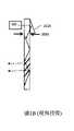
上述圖1A和1B是示出了用於將圖像照射耦入到波導中的兩個幾何結構的常規的基於波導的近眼顯示器的示意性側視圖;1A and 1B above are schematic side views of a conventional waveguide-based near-eye display showing two geometries for coupling image illumination into a waveguide;
上述圖1C是示出了使用第一組部分反射內表面和第二組部分反射內表面以在二維上擴展圖像投影儀的光學孔徑的常規的基於波導的近眼顯示器的正視圖;1C above is a front view illustrating a conventional waveguide-based near-eye display using a first set of partially reflective inner surfaces and a second set of partially reflective inner surfaces to expand the optical aperture of an image projector in two dimensions;
圖1D是與圖1C的波導類似並且與公開WO 2020/049542 A1的圖5A對應的波導的示意性等距視圖;Figure ID is a schematic isometric view of a waveguide similar to that of Figure 1C and corresponding to Figure 5A of publication WO 2020/049542 A1;
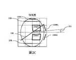
圖2A至圖2C分別是根據本發明的教導的通過光學系統的圖像傳播的角度表示的等距視圖、俯視圖和側視圖;2A-2C are isometric, top, and side views, respectively, of angular representations of image propagation through an optical system in accordance with the teachings of the present invention;
圖3A是根據本發明的方面的教導構造和操作的、示出圖像照射從耦入區域傳播到第一組部分反射表面(小平面)以及從第一組小平面傳播到第二組小平面的光導光學元件(LOE或波導)的示意性正視圖;3A is a view constructed and operative in accordance with the teachings of aspects of the present invention showing image illumination propagating from a coupling region to a first set of partially reflective surfaces (facets) and from the first set of facets to a second set of facets A schematic front view of a light-guiding optical element (LOE or waveguide);
圖3B是類似於圖3A的示出了為單個視點提供視場(field of view,FOV)所需的小平面位置的理論軌跡的視圖;3B is a view similar to FIG. 3A showing theoretical trajectories of facet positions required to provide a field of view (FOV) for a single viewpoint;
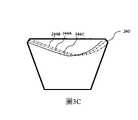
圖3C是類似於圖3B的示出了用於在允許觀看位置的“眼動箱”(eye-motion box,EMB)上提供FOV的小平面位置的對應的成組軌跡的視圖;Fig. 3C is a view similar to Fig. 3B showing the corresponding grouped trajectories of facet positions for providing FOV on an "eye-motion box" (EMB) allowing viewing positions;
圖3D是類似於圖3A的示出了為了跨越圖3C所示的軌跡所需的小平面位置和尺寸的視圖;Figure 3D is a view similar to Figure 3A showing the facet bits required to span the trajectory shown in Figure 3Cview of placement and size;
圖3E是類似於圖3C的其中根據由使用呈傾斜角度的第一組小平面產生的幾何要求進一步增加軌跡的視圖;3E is a view similar to FIG. 3C in which trajectories are further increased according to the geometric requirements resulting from the use of the first set of facets at oblique angles;
圖3F是圖3D的其中小平面包含區域由對應的多邊形劃界且第一組小平面由凹多邊形劃界的LOE的示意性表示;3F is a schematic representation of the LOE of FIG. 3D in which the facet-containing area is bounded by corresponding polygons and the first set of facets is bounded by concave polygons;
圖3G是類似於圖3F的其中包含第一組小平面的凹多邊形被細分為多個非凹形塊或片的視圖;Figure 3G is a view similar to Figure 3F in which a concave polygon comprising a first set of facets is subdivided into a plurality of non-concave blocks or slices;
圖3H是示出如何組裝這些塊以產生用於隨後切片以形成多個LOE的圖3G的結構的示意性等距視圖;3H is a schematic isometric view showing how the blocks are assembled to produce the structure of FIG. 3G for subsequent slicing to form multiple LOEs;
圖4A是類似於圖3A的示出了用於生成具有如圖4B所示的角度尺寸的矩形視場的實現方式的示例性尺寸的視圖;4A is a view similar to FIG. 3A showing exemplary dimensions of an implementation for generating a rectangular field of view having the angular dimensions shown in FIG. 4B;
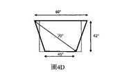
圖4C是類似於圖3A的示出了用於生成具有如圖4D所示的角度尺寸的梯形視場的實現方式的示例性尺寸的視圖;4C is a view similar to FIG. 3A showing exemplary dimensions of an implementation for generating a trapezoidal field of view having the angular dimensions shown in FIG. 4D;
圖5A是類似於圖4A的示出了圖像投影儀和用於將圖像照射引入LOE的耦入稜鏡的視圖;FIG. 5A is a view similar to FIG. 4A showing an image projector and an in-coupler for introducing image illumination into the LOE;
圖5B是圖5A的耦入稜鏡的示意性等距視圖;FIG. 5B is a schematic isometric view of the coupled-in sensor of FIG. 5A;
圖5C是圖5A的示出了本發明的示例性實施方式所需的尺寸的耦入稜鏡的側視圖;FIG. 5C is a side view of the coupling coil of FIG. 5A showing the dimensions required by an exemplary embodiment of the present invention;
圖5D示出了本發明的採用附接至LOE的主外表面的耦入稜鏡的變型實現方式;Figure 5D shows a variant implementation of the present invention employing an in-coupling element attached to the main outer surface of the LOE;
圖6A是類似於圖5A的示出了與耦入稜鏡集成的集成雷射掃描圖像投影儀的使用的示意性正視圖;FIG. 6A is a schematic front view similar to FIG. 5A illustrating the use of an integrated laser scanning image projector integrated with an in-coupling camera;
圖6B是與圖6A的耦入稜鏡集成的集成雷射掃描圖像投影儀的示意性側視圖;FIG. 6B is a schematic side view of an integrated laser scanning image projector integrated with the in-coupling sensor of FIG. 6A;
圖7A是採用傾斜反射器耦合佈置和耦入稜鏡並且採用外部準直光學器件的耦入佈置的示意性側視圖;7A is a schematic side view of a coupling arrangement employing a tilted reflector and a coupling arrangement and employing external collimating optics;
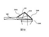
圖7B是類似於圖7A的其中組合了傾斜反射器耦合佈置和耦入稜鏡並且尺寸減小的視圖;FIG. 7B is a view similar to FIG. 7A in which a tilted reflector coupling arrangement and an in-coupling mirror are combined and reduced in size;
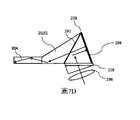
圖7C是與圖7A類似的採用偏振分束器並且將反射準直光學器件集成到反射耦入佈置中的視圖;Figure 7C is similar to Figure 7A using a polarizing beam splitter and integrating reflective collimation optics intoReflections are coupled into views in the arrangement;
圖7D是類似於圖7C但使用外部準直光學器件的視圖;Figure 7D is a view similar to Figure 7C but using external collimation optics;
圖8A是類似於圖5A但其中耦入稜鏡與波導的一部分集成的視圖;FIG. 8A is a view similar to FIG. 5A but with the coupling element integrated with a portion of the waveguide;
圖8B是圖8A的耦入稜鏡的示意性等距視圖;FIG. 8B is a schematic isometric view of the coupled-in sensor of FIG. 8A;
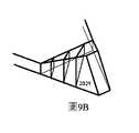
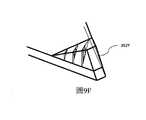
圖9A是圖8A的耦入稜鏡的被實現為在LOE的邊緣表面處接合至LOE的耦入稜鏡的示意性側視圖;FIG. 9A is a schematic side view of the in-coupling foil of FIG. 8A implemented as bonded to the LOE at the edge surface of the LOE;
圖9B和圖9C是圖9A的示出了在稜鏡內分別包括全部的部分反射小平面或部分的部分反射小平面的耦入稜鏡的示意性等距視圖;Figures 9B and 9C are schematic isometric views of the in-coupling apertures of Figure 9A showing the inclusion of all or a portion of the partially reflective facets, respectively, within the aperture;
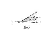
圖9D是圖8A的耦入稜鏡被實現為接合至LOE的主外表面之一的耦入稜鏡的示意性側視圖;FIG. 9D is a schematic side view of the in-coupling foil of FIG. 8A implemented as an in-coupling foil engaged to one of the major outer surfaces of the LOE;
圖9E和圖9F是圖9D的示出了在稜鏡內分別包括全部的部分反射小平面或部分的部分反射小平面的耦入稜鏡的示意性等距視圖;FIGS. 9E and 9F are schematic isometric views of the in-coupled iris of FIG. 9D showing the inclusion of all or a portion of the partially reflective facets, respectively, within the iris;
圖10A是類似於圖2C的示出了經投影的圖像的視場內的兩個特定點的角度表示的側視圖;Figure 10A is a side view similar to Figure 2C showing an angular representation of two specific points within the field of view of the projected image;
圖10B是類似於圖4A的示出了與圖10A的兩個點對應的圖像光傳播路徑的局部視圖;Fig. 10B is a partial view similar to Fig. 4A showing the image light propagation paths corresponding to the two points of Fig. 10A;
圖10C和圖10D是分別指示這兩個場點的射入角、以及場點應當遇到的第一反射小平面的對應的期望位置的耦入稜鏡的側視圖;Figures 10C and 10D are side views of the in-coupling plane indicating, respectively, the angles of incidence of the two field points, and the corresponding desired positions of the first reflective facets that the field points should encounter;
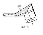
圖11A至圖11C是分別類似於圖7A、圖7C和圖7D的示出了在耦合稜鏡內具有部分反射小平面的這些幾何結構的實現方式的視圖;Figures 11A-11C are views similar to Figures 7A, 7C, and 7D, respectively, showing implementations of these geometries with partially reflective facets within the coupling layer;
圖11D是類似於圖6B的示出了在耦合稜鏡內具有部分反射小平面的這種幾何結構的實現方式的視圖;FIG. 11D is a view similar to FIG. 6B showing an implementation of such a geometry with partially reflective facets within the coupling field;
圖12A是用於根據本發明的生產方法進行組裝的具有均根據圖3D的LOE的不同平面所需的圖案選擇性地部署的部分反射塗層的一系列板的示意性等距視圖;12A is a schematic isometric view of a series of panels with partially reflective coatings each selectively deployed according to a desired pattern for the different planes of the LOE of FIG. 3D for assembly in accordance with the production methods of the present invention;
圖12B是通過將圖12A的一系列板接合在一起而形成的板的堆疊的示意性等距視圖;12B is a schematic isometric view of a stack of panels formed by joining the series of panels of FIG. 12A together;
圖12C是通過沿所指示的虛線對圖12B的堆疊進行切片而形成的塊的示意性等距視圖;Figure 12C is a schematic isometric view of a block formed by slicing the stack of Figure 12B along the indicated dashed lines;
圖12D是通過沿所指示的虛線對圖12C的塊進行切片而形成的LOE(的一部分)的示意性等距視圖;Figure 12D is a schematic isometric view of a (portion of) LOE formed by slicing the block of Figure 12C along the dashed lines indicated;
圖13是採用氣隙和鏡面的耦入構造的示意性側視圖;Figure 13 is a schematic side view of a coupling configuration employing an air gap and mirror;
圖14A和圖14B是分別類似於圖2A和圖2C的示出了在呈傾斜定向的第一組部分反射表面的情況下通過光學系統的圖像傳播的視圖;Figures 14A and 14B are views similar to Figures 2A and 2C, respectively, illustrating image propagation through an optical system with a first set of partially reflective surfaces in an oblique orientation;
圖14C是類似於圖3F的用於針對圖14A和圖14B中描述的圖像傳播而優化的LOE的實現方式的視圖;Figure 14C is a view similar to Figure 3F for an implementation of an LOE optimized for the image propagation described in Figures 14A and 14B;
圖15是採用分束器以用射入圖像及其共軛填充波導的側耦入構造的示意性側視圖;Figure 15 is a schematic side view of a side-coupling configuration employing a beam splitter to fill the waveguide with an incident image and its conjugate;
圖16A是根據本發明的採用呈高傾斜的第二組部分反射表面的變型實現方式的通過LOE的第二區域的圖像傳播的角度表示的側視圖;16A is a side view of an angular representation of image propagation through a second region of the LOE in accordance with a variant implementation of the present invention employing a second set of partially reflective surfaces that are highly inclined;
圖16B是根據圖16A的光學幾何結構實現的LOE的第二區域的示意性側視圖;Figure 16B is a schematic side view of a second region of the LOE implemented according to the optical geometry of Figure 16A;
圖16C是示意性地指示用於圖16B的實現方式的小平面的反射率的優選角度依賴性的曲線圖;Figure 16C is a graph schematically indicating the preferred angular dependence of reflectivity for the facets of the implementation of Figure 16B;
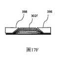
圖17A是與圖12A的板類似的具有選擇性部署的部分反射塗層的板的示意性等距視圖;17A is a schematic isometric view of a panel similar to the panel of FIG. 12A with selectively deployed partially reflective coatings;
圖17B是示出利用陡峭邊緣實現的塗覆區域的放大的示意性側視圖;17B is an enlarged schematic side view showing a coating area achieved with a steep edge;
圖17C是使用凸起的掩模來生成具有逐漸變化的厚度的邊緣區域的塗層的示意性圖示;17C is a schematic illustration of the use of a raised mask to generate a coating with edge regions of gradually varying thickness;
圖17D是使用圖17C的原理來沉積具有逐漸變化厚度的邊緣區域的多層塗層的示意性圖示;17D is a schematic illustration of using the principles of FIG. 17C to deposit a multilayer coating with edge regions of gradually varying thickness;
圖17E是使用第二凸起掩模在未被第一工藝塗覆的區域中生成互補透明塗層的示意性圖示;以及17E is a schematic illustration of the use of a second bump mask to generate a complementary clear coating in areas not coated by the first process; and
圖17F是示出由參照圖17D和圖17E描述的塗覆工藝的順序產生的部分反射區域的示意性側視圖。Figure 17F is a schematic side view showing the partially reflective area resulting from the sequence of coating processes described with reference to Figures 17D and 17E.
本發明是一種用於將在耦入區域處射入的圖像照射引導至眼動箱以供使用者觀看的光學系統。The present invention is an optical system for directing image illumination incident at a coupling region to an eye-tracking box for viewing by a user.
通過介紹,在圖1C所示類型的近眼顯示器的上下文中,已經發現,通過以“淺角度”將圖像照射射入波導中,可以提供特別有利的幾何特性,並且特別是使給定角視場所需的尺寸最小化。從而意味著所有圖像照射僅入射在第一組小平面和第二組小平面二者的一側上。一般地,在淺角度實現方式中,每個圖像的至少一部分位於距離波導的外表面的平面約15度內,並且更優選地位於約10度內。這產生從圖像投影儀到觀察者的眼睛的縮短的光路徑,並且因此還使得對於給定角視場能夠減小光學部件的尺寸。本發明涉及利於這樣的顯示器的淺角度實現方式的多個方面,這提出了特定的設計挑戰,特別是關於耦入構造的設計挑戰。然而,應當注意,本文中所描述的本發明的各個方面不限於淺角度實現方式,並且還可以適用於其他實現方式。By way of introduction, in the context of a near-eye display of the type shown in Figure 1C, it has been found that by injecting the image illumination into the waveguide at a "shallow angle", particularly advantageous geometrical properties can be provided, and in particular a given angle of view The required size of the field is minimized. This means that all image illumination is incident on only one side of both the first and second set of facets. Generally, in shallow angle implementations, at least a portion of each image is located within about 15 degrees, and more preferably within about 10 degrees, from the plane of the outer surface of the waveguide. This results in a shortened light path from the image projector to the viewer's eye, and thus also enables the size of the optics to be reduced for a given angular field of view. The present invention relates to aspects that facilitate shallow angle implementations of such displays, which present specific design challenges, particularly with regard to coupling-in configurations. It should be noted, however, that the various aspects of the invention described herein are not limited to shallow angle implementations, and may also be applicable to other implementations.
圖2A至圖2C示出了圖像在根據本發明的波導中傳播時的圖像的角度極性表示。圖2A示出等距視圖,圖2C示出側視圖,以及圖2B示出與從波導前方的視圖對應的俯視圖(相對於圖2A)。Figures 2A to 2C show angular polar representations of images as they propagate in a waveguide according to the invention. FIG. 2A shows an isometric view, FIG. 2C shows a side view, and FIG. 2B shows a top view (relative to FIG. 2A ) corresponding to the view from the front of the waveguide.
波導具有全內反射(total-internal-reflection,TIR)邊界圓228,指示這些圓內的圖像不受TIR影響,並且將被耦出以離開波導。The waveguides have total-internal-reflection (TIR) bounding
將圖像220A1耦入到波導中並且通過來回TIR傳播到220A2。這些圖像沿著非常淺的軌跡沿著波導傳播,其中圖像的最淺部分僅與波導平面成7度(在圖2C中示出為角度221)。在該實現方式中,小平面224(等同於圖1C的206L)垂直於波導,並且因此將圖像220A1和220A2分別直接反射到220B1和220B2上。當圖像220B1和220B2沿波導傳播時,它們通過TIR耦合。在LOE的第二部分中,小平面226(等同於圖1C中的206V)將圖像220B2從波導耦出到朝向觀察者的圖像220C上。Image 220A1 is coupled into the waveguide and propagated to 220A2 by TIR back and forth. These images propagate along the waveguide along very shallow trajectories, with the shallowest portion of the images only 7 degrees from the waveguide plane (shown as
作為一個非限制性示例,本文所示的圖示主要涉及射入折射率為1.6的波導中的具有4:3的縱橫比和70度的對角線場的圖像。此處示出的設計在遠離波導35mm的眼球中心處生成完整圖像(包括出瞳距離、眼球半徑和邊緣)。本領域的普通技術人員基於本文的描述可以容易地實現針對不同視場和縱橫比的這些實現方式的調整。As a non-limiting example, the illustrations shown herein primarily relate to images with a 4:3 aspect ratio and a 70 degree diagonal field incident into a waveguide with an index of refraction of 1.6. The design shown here produces a complete image (including exit pupil distance, eye radius and edge) at the center of the eyeball 35 mm away from the waveguide. Adjustments to these implementations for different fields of view and aspect ratios can be readily accomplished by those of ordinary skill in the art based on the descriptions herein.
本發明的一個方面涉及對波導的負責第一維光學孔徑擴展的第一部分中的部分反射表面(或“小平面”)的部署進行優化。在公開為WO 2020/049542 A1(“’542公開”)的較早專利申請中,已經提出將小平面選擇性地佈置在包圍小平面的包絡內,這些小平面是將圖像照射遞送至要從其觀看圖像的眼動箱所需的。One aspect of the invention relates to optimizing the deployment of partially reflective surfaces (or "facets") in the first portion of the waveguide responsible for first-dimensional optical aperture expansion. in public as WOIn an earlier patent application of 2020/049542 A1 ("the '542 publication"), it has been proposed to selectively arrange facets within an envelope surrounding the facets that deliver image illumination to the image from which the image is to be viewed. Like the eye-tracking box required.
在該公開的圖5A中示出了小平面的最終部署的示例,其在此再現為圖1D。在該實現方式中,一種用於將在耦入區域15處射入的圖像照射引導至眼動箱26以供使用者的眼睛觀看的光學系統採用由透明材料形成的光導光學元件(LOE)12,該光導光學元件具有:第一區域16,其包含具有第一取向的平面的、相互平行的第一組部分反射表面17,以及第二區域18,其包含具有第二取向的平面的、相互平行的第二組部分反射表面19,第二取向不平行於第一取向。一組相互平行的主外表面24跨第一區域和第二區域延伸,使得第一組部分反射表面和第二組部分反射表面二者位於主外表面之間。第二組部分反射表面19與主外表面24成斜角,使得通過主外表面處的內反射在LOE內從第一區域傳播到第二區域的圖像照射的一部分從耦出區域28朝向眼動箱26耦出LOE。第一組部分反射表面17被定向成使得來自耦入區域的、通過主外表面處的內反射在LOE內傳播的圖像照射的一部分朝向第二區域偏轉。An example of the final deployment of facets is shown in Figure 5A of this publication, reproduced here as Figure ID. In this implementation, an optical system for directing the image illumination incident at the
根據’542公開的教導,將LOE的第一區域16的在有用小平面的包絡之外的某些部分實現為光學連續體(即,沒有部分反射內表面),從而減少不想要的重影反射。然而,在凸多邊形包絡內,將小平面實現為填充凸多邊形的整個寬度,如圖中所示。因此,從位於耦入區域遠側的一側上的小平面反射的視場的一部分在到達將視場的該一部分遞送到眼動箱的小平面之前穿過長的一系列部分反射小平面。According to the teachings of the '542 disclosure, certain portions of the
根據本發明的一個方面,將給定視場遞送到眼動箱所需的小平面的區域被進一步細化以生成限定所需的小平面位置的凹多邊形,從而去除中間小平面的一部分,該部分否則將不必要地使被引導以提供由距耦入區域最遠的小平面反射的場的部分的圖像照射衰減。According to one aspect of the invention, the area of facets required to deliver a given field of view to the eye-tracking box is further refined to generate concave polygons that define the desired facet locations, thereby removing a portion of the middle facet, which Parts that would otherwise unnecessarily attenuate image illumination for parts of the field that are directed to provide the field reflected by the facet furthest from the coupling-in region.
因此,如圖3D中所示,第一組部分反射表面(此處標記為206L)包括:第一部分反射表面17A,其靠近耦入區域240,以貢獻於用戶在眼動箱處觀看到的視場(FOV)的第一部分;第三部分反射表面17C,其在耦入區域遠側,以貢獻於用戶在眼動箱處觀看到的FOV的第三部分;以及第二部分反射表面17B,其位於第一部分反射表面與第三部分反射表面之間的中間平面22中,以貢獻於用戶在眼動箱處觀看到的FOV的第二部分。在圖3D所示的示例中,第一部分反射表面(小平面)17A貢獻於FOV的右側,第三部分反射表面(小平面)17C貢獻於FOV的左側,並且第二部分反射表面(小平面)17B貢獻於FOV的中央區域。本發明的該方面的特定特徵在於,將第二部分反射表面17B部署在中間平面22的子區域中,使得從耦入區域傳播到第三部分反射表面(箭頭23)並且貢獻於用戶在眼動箱處觀看到的視場的第三部分的圖像照射穿過中間平面22而不穿過第二部分反射表面17B。Thus, as shown in FIG. 3D, the first set of partially reflective surfaces (here labeled 206L) includes: a first partially
在該上下文中,應當注意,術語“靠近”、“遠離”和“中間”在本文中用於表示對於感興趣的點或區域(在這種情況下為耦入區域240)而言的相對位置,並且是指相對更接近(靠近)耦入區域或距耦入區域相對較遠(遠離)的小平面,或者小平面“朝向中間”(中部),而不必根據任何具體的幾何限定表示最近的、最遠的或中央的小平面。In this context, it should be noted that the terms "closer," "farther," and "intermediate" are used herein to denote relative positions with respect to a point or area of interest (in this case coupling-in area 240). , and refers to facets that are relatively closer (closer to) or relatively farther (farther) from the coupling-in region, or facet "towards the middle" (middle), without necessarily denoting the closest according to any specific geometrical constraints , the furthest or central facet.
現在將提供概念性的說明,以利於更好地理解幾何光學考慮,該幾何光學考慮使得對於本發明的該方面的給定實現方式的優選的設計參數。應當注意,僅出於資訊目的給出了該說明,但是所要求保護的本發明的效用不依賴於該說明的任何方面的準確性,並且所要求保護的本發明的有效且有利的實現方式可以替選地通過經驗方法來實現。A conceptual illustration will now be provided to facilitate a better understanding of the geometrical optics considerations that lead to preferred design parameters for a given implementation of this aspect of the invention. It should be noted that this description is given for informational purposes only, but that the utility of the claimed invention does not depend on the accuracy of any aspect of this description, and that efficient and advantageous implementations of the claimed invention may be Alternatively this is achieved by empirical methods.
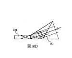
圖3A示出了具有與以上提及的示例性FOV對應的參數的經投影圖像的少數選定光束的正視圖。實線表示橫向射入波導的圖像的光束,並且虛線表示當光束豎直傳播時橫向孔徑擴展和反射之後的光束。在整個文檔中應當注意的是,在不發生結構上的固有改變的情況下,可以將描述橫向擴展之後是豎直擴展的任何示例改變為豎直擴展之後是橫向擴展。這可以簡單地通過將上述圖式旋轉90度來例示。Figure 3A shows a front view of a few selected beams of projected images with parameters corresponding to the exemplary FOV mentioned above. The solid line represents the beam incident transversely to the image of the waveguide, and the dashed line represents the beam after lateral aperture expansion and reflection as the beam propagates vertically. It should be noted throughout this document that any example describing a horizontal expansion followed by a vertical expansion can be changed to a vertical expansion followed by a horizontal expansion without an inherent change in structure. This can be exemplified simply by rotating the above figure by 90 degrees.
所有光束從耦入區域240中的入射光瞳發射。光束在波導內傳播直到被一組平行嵌入的反射器206L(小平面)反射。假定該圖中的小平面垂直於波導的外表面。因此,每條線(實線後跟虛線)表示投影到觀察者眼睛裡的圖像場的不同橫向截面。每個截面的豎直場由以通過TIR(這樣的內反射在圖1A的側視圖中示出)反射的不同角度傾斜傳播(進入頁面)的多個交疊光束(如從前方觀察)照射。All beams are emitted from the entrance pupil in the coupling-in
出於簡化幾何分析的目的,首先假設只需要用整個橫向場照射眼球中心208。這在理論上可以通過使無限小的橫向小平面206L沿著圖3B中的表示為244A的軌跡彼此無限靠近地放置來實現。然而,適應眼球中心的橫向位移的要求(例如由於用戶之間的瞳孔間距離的變化)決定曲線244A的位移。圖3C示意性地示出了眼球中心208的三個橫向位置為244A、244B和244C的曲線。為了覆蓋眼動箱的所需寬度,需要對小平面進行加寬。For the purpose of simplifying the geometric analysis, it is first assumed that only the center of the
其他要求包括:Other requirements include:
˙小平面之間存在有限的最小距離(即,小平面不能無限靠近)˙ There is a finite minimum distance between facets (i.e. facets cannot be infinitely close together)
˙孔徑尺寸不能太小;˙Aperture size should not be too small;
˙小平面必須朝向豎直擴展小平面206V投射連續的反射。˙ The facet must project a continuous reflection towards the vertically expanding
圖3D示出了適合於上述條件的有限尺寸的小平面206L。小平面的長度可以根據小平面間距和諸如折射率、經投影的場的大小以及圖像耦入區域(射入)240的位置的其他光學參數而變化。Figure 3D shows a
在橫向擴展小平面206L與LOE的主外表面成斜角的情況下,將圖像射入相對於波導的軸旋轉的波導中,並且來自小平面206L的反射使圖像旋轉到所需取向。因此,用於投影到眼球中心208上的曲線將看起來像圖3C,並且當另外考慮橫向眼動箱所需的擴展時,曲線看起來像圖3E,圖3E示出了曲線244A、244B和244C的進一步倍增。因此,這需要比用於第一擴展的具有正交小平面的對應的實現方式稍微更寬的小平面。With laterally expanding
參照圖3F可以更好地理解本發明的該方面的某些優點。在SL處描述了橫向擴展小平面的區域,而該區域上方的“凹陷”的區域為SD並且豎直擴展小平面的區域為SV。由於區域SL的凹多邊形形式,從耦入區域(入口)240橫向傳播的光在區域SL中被向下反射之前主要在透明區域SD中傳播。在透明區域中的傳播減少了通過反射到不期望的方向的圖像照射的損失,從而提高了波導效率。此外,不存在來自區域SD的由小平面對景物的不期望的反射,從而基本上減少了來自波導的閃爍和重像。Certain advantages of this aspect of the invention may be better understood with reference to Figure 3F. The area of laterally expanding facets is described at SL, while the area of the "sink" above this area is SD and the area of vertically expanding facets is SV. Due to the concave polygonal form of the region SL, light propagating laterally from the coupling-in region (inlet) 240 propagates mainly in the transparent region SD before being reflected downwards in the region SL. Propagation in the transparent region reduces the loss of image illumination by reflection into undesired directions, thereby increasing the waveguide efficiency. Furthermore, there is no undesired reflection of the scene from the facet from the area SD, thereby substantially reducing flicker and ghosting from the waveguide.
圖3G和3H中示出了用於產生具有“凹陷”區域SD的區域(橫向擴展截面)SL的一個可能的方法。包括區域SD和區域SL的部分被細分為如圖3G中區域指定300中的粗輪廓所指示的塊。圖3H示出了如何將這種結構從具有適當面角的透明稜鏡302與具有適當小平面角的三個板(示出為沿著板的線)組裝在一起,這三個板一起抵靠稜鏡302的相應表面安置並且彼此抵靠以形成所示的組裝結構。該結構與附加的透明稜鏡和LOE的豎直擴展部分組合以生成整體結構。Figures 3G and 3H show the region used to create a "recessed" region SD (horizontalA possible method to expand the cross section) SL. The part including the area SD and the area SL is subdivided into blocks as indicated by the thick outline in the
可選地,可以對組合的稜鏡和板切片,或者可以首先附接至要被一起切片的另一堆疊以生成具有其所有部分的波導。Alternatively, the combined wafer and plate can be sliced, or can be first attached to another stack to be sliced together to create a waveguide with all its parts.
如上所述的波導的尺寸在圖4A中示出,得到如圖4B所示的圖像場角度大小。注意,最橫向擴展的光束250僅照射圖像的下角,從而需要大的波導面積,同時僅對圖像的一小部分有貢獻。在某些應用中,提供非矩形FOV,並且特別是提供如圖4D所示的梯形圖像場是可接受的,或者甚至是有利的。在這種情況下,示出了具有與圖4B相同的總面積的圖像(為了比較,在圖4D中用虛線示出),但是分佈為梯形,其中頂部的場比底部的場寬。生成該FOV的LOE在圖4C中以相應的尺寸示出。在這種情況下,橫向邊緣光束252豎直地照射所有場(以相應的不同角度進入紙張頁),因此使得更有效地使用LOE尺寸。因此,圖4C的波導的尺寸基本上小於圖4A的波導的尺寸,如相同總FOV面積的示例性尺寸所示。隨後的描述在圖4A的構造的非限制性示例性上下文中示出本發明的其他方面,但應當理解,可以使用相同原理來實現諸如圖4C的構造的構造。The dimensions of the waveguide as described above are shown in Figure 4A, resulting in the image field angle size shown in Figure 4B. Note that the most laterally expanded
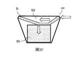
將淺圖像射入波導需要相對大的耦合稜鏡202。圖5A按比例示出了具有橫向孔徑(入射光瞳)203L和耦合稜鏡202M的波導。示意性地示出了圖像投影儀200。圖5B是具有豎直孔徑203V和橫向孔徑203L的耦合稜鏡202M的等距視圖,豎直孔徑203V和橫向孔徑203L二者位於同一平面以限定矩形孔徑。圖5C示出了耦合稜鏡202M的側視圖,對於1.7mm厚度波導,其需要14mm長的耦合稜鏡,該耦合稜鏡被設計成將來自所有場角的光耦合到波導中。光束262的一部分在通過孔徑(光瞳)203V進入波導204之前從稜鏡的底部反射。波導上方的耦合稜鏡202M的高度為6.4mm,這在許多應用中是可接受的。然而,通過耦合稜鏡202M射入圖像所需的圖像投影儀200的尺寸也佔用空間和體積,並且在許多應用中將是不可接受的。Injecting a shallow image into the waveguide requires a relatively
耦合稜鏡202M(以及本文描述的其他稜鏡)優選地具有平行於波導面以用於一致反射的下部面,而上部面和側部面不需要特定的光學特性,因此它們的形狀可以不同於這些圖中所示的形狀。The
圖5D示出了其中耦合稜鏡202L位於波導上方並且入射光瞳是稜鏡面264的替選結構。在這種情況下,稜鏡和所需的投影儀大於圖5A至圖5C中的稜鏡和投影儀,使得這種構造不是最優的。FIG. 5D shows an alternative configuration in which the
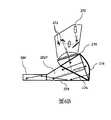
圖6A和圖6B示出了用於減小耦合佈置和圖像投影儀的整體尺寸的一種選擇,其示出了圖像投影儀與耦合稜鏡的集成。此處通過非限制性示例的方式示出了掃描雷射圖像投影儀,但是可以使用基於另一類型的圖像生成器的圖像投影儀來實現相同的原理,例如採用矽基液晶(Liquid Crystal on Silicon,LCOS)空間光調製器或者微型發光二極體(Light Emitting Diode,LED)圖像生成器。Figures 6A and 6B illustrate one option for reducing the overall size of the coupling arrangement and image projector, showing the integration of the image projector with the coupling lens. A scanning laser image projector is shown here by way of non-limiting example, but the same principle can be implemented using an image projector based on another type of image generator, such as liquid crystal on silicon (Liquid Crystal on Silicon, LCOS) spatial light modulator or miniature light-emitting diode (Light Emitting Diode, LED) image generator.
圖6A示出了附接至波導204的耦合稜鏡202P。圖6B示出了集成(嵌入)的圖像投影儀的側視圖。雷射器270將偏振光束引導至掃描鏡272上,掃描鏡272掃描跨微透鏡陣列(micro-lens array,MLA)或漫射器274的中間圖像平面。經掃描的光穿過漫射器並且從偏振分束器276反射到準直反射鏡278(與四分之一波片組合)上。經反射的光穿過偏振分束器(Polarization Beam Splitter,PBS)276進入耦合稜鏡202P。因此,該耦合稜鏡也用作PBS 276的一部分。光的一部分直接進入波導,部分在進入波導之前被下部面279反射,從而利用圖像及其共軛填充波導的孔徑。FIG. 6A shows the
附帶地,無論在本文中將PBS佈置示出為依次反射然後透射光,或者相反的情況,應當理解適當地放置半波片(用於單次透射)或四分之一波片(用於兩次透射)以實現所述功能所需的偏振旋轉。偏振旋轉元件將不在每種情況下提及。Incidentally, whether the PBS arrangement is shown herein as sequentially reflecting and then transmitting light, or vice versa, it should be understood that a half-wave plate (for single transmission) or a quarter-wave plate (for two transmissions) is appropriately placed sub-transmission) to achieve the required polarization rotation for said function. Polarization rotating elements will not be mentioned in every case.
圖7A至圖7D示出了用於將圖像投影儀與耦合稜鏡進行組合的替選結構。圖7A示出了來自圖像生成器(未示出,但如前所述,可以是掃描雷射器、LCOS或其他)的光被折射透鏡280準直(圖中光束來自不同場點,因此不平行)、進入稜鏡部282並且由鏡284反射進入耦合稜鏡(稜鏡部)202Q並且進入波導204。在該構造中,可以將稜鏡部282和耦合稜鏡202Q組合成單個稜鏡,如圖7B所示。此外,在這種情況下不需要對光進行偏振。Figures 7A-7D illustrate alternative structures for combining an image projector with a coupling lens. Figure 7A shows light from an image generator (not shown, but as previously mentioned, could be a scanning laser, LCOS, or other) collimated by a refractive lens 280 (beams in the figure come from different field points, so non-parallel), enters the
圖7B的結構採用與圖7A等同的反射器結構,但具有較小的稜鏡。此處,對於類似的輸出參數,類似於圖5C中的耦合稜鏡202M,稜鏡長度約為14mm。然而,高度將僅為3.2mm,為耦合稜鏡202M的一半。如本文中描述的所有稜鏡中,稜鏡283的上部(非反射)面優選是吸收性的。此處根據上光束260(在圖5C中限定)繪製,但是由於上表面不是光學上重要的,所以其可以更高和/或具有其他形狀。The structure of Figure 7B employs the same reflector structure as Figure 7A, but with a smaller aperture. Here, for similar output parameters, similar to the
該稜鏡還可以設置有耦合構造,該耦合構造包括在其下部面處的等同於下面參照圖7C和圖7D描述的元件286或228的低折射率部分。該介面可以用於附接至PBS作為圖像投影儀。The crystal may also be provided with a coupling formation including a low index portion at its lower face equivalent to
圖7C示出了與穿過介面286進入稜鏡(PBS部)290並且由PBS 292反射到反射準直透鏡294上的圖像(來自MLA、掃描雷射器、LCOS或其他圖像生成器)對應的發散偏振光的射入。經反射的準直光穿過PBS 292進入耦合稜鏡202Q並且進入波導204。在這種結構中,光中的一些被稜鏡290和耦合稜鏡202Q的下部反射,因此這些表面需要具有良好的圖像品質並且是連續的。介面286可以是空氣,也可以是低折射率介質(相對於稜鏡290),使得對於從反射準直透鏡294反射的光將發生TIR。FIG. 7C shows an image (from MLA, scanning laser, LCOS, or other image generator) that passes through
圖7D示出了類似於圖7C的、但是具有對光準直的外部光學器件(例如,折射透鏡296)和平坦反射器298的佈置。FIG. 7D shows an arrangement similar to that of FIG. 7C , but with light collimating external optics (eg, refractive lens 296 ) and
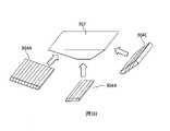
現在轉向圖8A和圖8B,這些圖示出根據本發明的另一方面的替選構造,其中,耦合稜鏡與波導的一部分集成,而不是作為圖5A所示的延伸。圖8A示出了波導204頂部上的耦合稜鏡202Y(虛線區域)。因此,圖像投影儀(生成器)200定位成更靠近波導並且具有更小的尺寸。在波導中傳播的所有光線繼續從耦入區域(點)240出現,因此橫向孔徑203L2位於與先前實施方式相同的位置處。然而,此處豎直孔徑203V位於稜鏡的端部,其中稜鏡的加厚部分與限定LOE的主要部分的主外表面相遇。圖8B以等距視圖示出了耦合稜鏡的形狀。兩個孔徑203L2和203V2具有與先前描述的相同的寬度,但是由於位置的分離,稜鏡在孔徑203L2處豎直地伸長。Turning now to Figures 8A and 8B, these figures illustrate an alternative configuration in accordance with another aspect of the present invention, wherein the coupling element is integrated with a portion of the waveguide, rather than as an extension of that shown in Figure 5A. FIG. 8A shows the
從圖8A中明顯的是,小平面中的一些(此處表示為206A和206B)位於稜鏡內。圖9A至圖9F示出了稜鏡202Y中這些小平面的多種可能的實現方式。為了清楚地呈現,此處省略了位於LOE的主要部分內的小平面。It is evident from Figure 8A that some of the facets (denoted here as 206A and 206B) are located within the horizon. Figures 9A-9F illustrate various possible implementations of these facets in H202Y. For clarity of presentation, the facets located within the main part of the LOE are omitted here.
圖9A示出了附接至波導的邊緣的稜鏡202Y,並且圖9B以等距方式示出了稜鏡中的小平面的放置。然而,由於不需要小平面在稜鏡的整個寬度上反射光(如圖8A中可以看出,圖8A示出小平面206A和206B的所需寬度是有限的),圖9C示出僅為稜鏡內的相應平面的一部分的反射部分(陰影區域)。FIG. 9A shows the
圖9D示出了其中通過在波導204(未示出204中的小平面)的頂部上附接使之成為相應形狀的塊來形成稜鏡202Y的替選構造。在圖9E中,示出了小平面在LOE厚度上方的202Y的整個截面上的相同結構,而在圖9F中,僅將反射區域實現為與僅最佳所需區域對應的陰影區域。Figure 9D shows an alternative configuration in which the
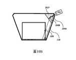
在某些情況下,可以將前面提及的集成圖像投影儀(圖6A至圖7D)與圖8A至圖9F的與LOE集成的耦合稜鏡組合在一起。參照圖10A至圖10D示出了這樣的實現方式中的某些幾何考慮。In some cases, the aforementioned integrated image projector (FIGS. 6A-7D) can be combined with the LOE-integrated coupling system of FIGS. 8A-9F. Certain geometric considerations in such an implementation are illustrated with reference to Figures 10A-10D.
圖10A示出了等同於圖2C、但是具有與小平面206A(圓形)和206B(方形)相關聯的兩個場點的標記的角度分佈的側視圖。在圖10B中示出了相同的場點。Figure 10A shows a side view of the angular distribution of the markers identical to Figure 2C, but with two field points associated with
圖10C示出其中陰影區域表示與206A相關聯的小平面的優選位置的波導-交疊耦合稜鏡的側視圖,並且圖10D示出針對206B的小平面的優選位置。此處示出PBS 292以供參考。明顯的是,交疊耦合稜鏡中的小平面的優選位置應該在PBS平面上方。在PBS平面之前實現小平面將導致所傳輸的圖像的失真。FIG. 10C shows a side view of the waveguide-overlapping coupling plane where the shaded area represents the preferred location of the facet associated with 206A, and FIG. 10D shows the preferred location of the facet for 206B.
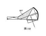
圖11A至圖11D是示出結合投影儀光學器件的耦合稜鏡的小平面的實現方式的側視圖。圖11A、圖11B和圖11C示出了將小平面部202T(標記為陰影區域)集成到另外分別類似於圖7A、圖7C和圖7D的構造的構造中。3D表示仍然如參照圖10A至圖10D所描述的那樣。Figures 11A-11D are side views showing implementations of facets incorporating coupling optics of projector optics. Figures 11A, 11B, and 11C illustrate the integration of
圖11D與圖6B相似,並且示出了在PBS取向相反的情況下,最好僅在PBS平面之後部分地實現小平面部202T2。因此,耦合稜鏡將稍微進一步延伸到橫向孔徑203L2之外(在圖8A至圖8B中示出)。Figure 11D is similar to Figure 6B and shows that with the PBS oriented opposite,The facet portion 202T2 is preferably implemented only partially behind the PBS plane. Therefore, the coupling pole will extend slightly further beyond the lateral aperture 203L2 (shown in Figures 8A-8B).
附帶地,如圖11D所示的小平面部202T2的部署也將適合於採用圖4C和圖4D的波導結構的構造。Incidentally, the deployment of the facet portion 202T2 as shown in Figure 1 ID would also be suitable for configurations employing the waveguide structures of Figures 4C and 4D.
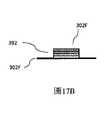
現在轉向圖12A至圖12D,作為以上參照圖3G至圖3H示出的生產過程的替選方案,可以基於對選擇性塗覆的板進行堆疊和切片來生產圖3D或圖3F的小平面圖案。在這種情況下,如圖12A所示以預定圖案塗覆板,圖12A示出了從以預定圖案302F塗覆的正面300F示出的一組板。這些圖案具有根據112中所示的所需塗覆小平面的寬度和位置。這些圖案優選地通過在塗覆時掩蔽波導的未塗覆部分來產生。還可以通過塗覆非反射塗層來僅塗覆304F中的板的面的其他部分,以保持平坦表面或者將通過304的透射光的相位保持為與通過稜鏡302的透射光的相位等同。Turning now to Figures 12A-12D, as an alternative to the production process shown above with reference to Figures 3G-3H, the facet pattern of Figure 3D or Figure 3F may be produced based on stacking and slicing selectively coated sheets . In this case, the panels are coated in a predetermined pattern as shown in Figure 12A, which shows a set of panels shown from the
圖12B示出了通過將部分塗覆的板接合在一起而形成的堆疊,其中虛線示出了堆疊上的切片平面。圖12C示出具有板300S和反射圖案302S的側視圖的一個切片。如圖12C中的虛線所示完成另一切片,以生成圖12D的最終上部,最終上部對應於圖3D的LOE的上部部分。Figure 12B shows a stack formed by joining partially coated plates together, where the dashed lines show the slice planes on the stack. Figure 12C shows a slice with a side view of
應當注意,可以改變切片的順序。還應當理解,圖12A至圖12D的圖示是高度示意性的,並且通常使用更多數目的板。It should be noted that the order of the slices can be changed. It should also be understood that the illustrations of Figures 12A-12D are highly schematic and that generally a greater number of plates are used.
減小耦合稜鏡202M的折射率也可以用於減小稜鏡尺寸並且從而使系統更緊湊。圖13示出了其中耦合稜鏡202M由與下波導平面312在同一平面中的鏡310和氣隙代替的這種構思的極端情況。將來自投影光學器件308的光引導至波導204的垂直入口306和鏡面310上。由於氣隙的折射率較低,光束的角度改變並且因此鏡的長度比耦合稜鏡202M的長度短。下光束262的角度現在是11.5度而不是之前的7度。因此,鏡長度現在是8.5mm而不是圖5C中的14mm。當光束進入波導時,光束的角度分佈如圖5C所示。鏡可以與波導交疊以用於機械附接。Reducing the index of refraction of the
可以使用低折射率玻璃稜鏡來實現採用低折射率材料的概念上類似的方法。當使用低折射率玻璃稜鏡時,可以對由光進入垂直入口(面)306的入射角生成的一些分散進行補償。A conceptually similar approach using low refractive index materials can be achieved using low refractive index glasses. When using a low index of refraction glass, some dispersion created by the angle of incidence of the light entering the vertical entrance (face) 306 can be compensated for.
在至此詳述的實施方式中,針對第一組小平面採用的小平面206L與LOE的主外表面正交,如圖2A至圖2C中詳述。在參照圖14A至圖14C示出的替選的一組實施方式中,使用呈傾斜角度的小平面336來實現第一組小平面。圖14A示出了用於傳輸淺角度圖像的這樣的系統的等距角度表示,而圖14B示出了該角度表示的相應的局部側視圖。該非限制性示例採用與圖4C和圖4D所示的最小尺寸的圖像等同的梯形FOV,儘管該結構也可以清楚地用於矩形FOV。In the embodiments detailed so far, the
在該結構中,初始橫向傳播圖像334A1通過TIR反射與圖像334A2耦合。通過相對於波導面成斜角的傾斜的小平面336,僅圖像334A2被朝向LOE的第二區域重定向成圖像334B1。如本領域已知的,小平面336優選地塗覆有多層介電塗層,以對於與圖像334A2對應的入射角範圍提供所需程度的部分反射率(如在所有上述實施方式中),同時在對於與圖像334A1對應的入射角範圍基本上是透明的,以使能量損失和不期望反射的形成最小化。當圖像334B1沿著波導的第二區域以淺角度傳播時,圖像334B1通過TIR耦合到圖像334B2。然後,圖像334B2通過小平面338(僅在圖14A中示出)以等同於圖2A至圖2C的小平面226的方式耦出為334C。In this configuration, initial laterally propagating image 334A1 is coupled to image 334A2 by TIR reflection. Only image 334A2 is redirected towards the second region of the LOE as image 334B1 by sloping
圖14C示出了與圖4C等同的波導覆蓋區,其中陰影區域340是第一組小平面336的最佳區域,而區域342是輸出耦合小平面338的最佳區域。FIG. 14C shows an equivalent waveguide footprint to FIG. 4C , where shaded
上述各種耦入稜鏡佈置被構造成將圖像及其共軛二者耦入LOE,以利用圖像“填充”波導。對於將淺角度圖像射入到波導中特別有吸引力的替選方法是如圖15所示將圖像直接射入到波導中。為了用射入圖像及其共軛填充波導370,波導370具有耦入區域372,耦入區域372具有沿波導的中心平面的部分反射器374。將部分反射器374最優選地實現為50%反射器,優選地對角度和消色差不敏感,例如部分鍍銀表面。The various in-coupling arrangements described above are configured to couple both the image and its conjugate into the LOE to "fill" the waveguide with the image. A particularly attractive alternative for injecting shallow angle images into the waveguide is to inject the image directly into the waveguide as shown in FIG. 15 . To fill the
在圖15中,示出了與場中的最低點相關聯的三個光束,並且三個光束因此是圖像照射的最淺光束。下光束(實線箭頭)穿過準直光學器件376和耦合稜鏡378並且進入波導。在一次反射之後,下光束通過部分反射器374經歷部分反射並且被分成兩束。中心光束(虛線)在入口處被分開,並且上光束(點劃線)沿著耦入區域(組合器)372被按一半分開。明顯的是,在光束被分開(從而在圖像與其共軛之間分開圖像照射)之後,波導被均勻地照射。因此,在光被耦出之後期望均勻的圖像。In Figure 15, the three beams associated with the lowest point in the field are shown, and the three beams are therefore the shallowest beams illuminated by the image. The lower beam (solid arrow) passes through the
如果部分反射器374具有50%的反射率和50%的透射率,那麼對於與圖5C的長度(在本示例中為14mm)等同的長度,波導將被均勻地照射。在該構造中,照射光學器件376的孔徑非常小,因為光學器件幾乎鄰近波導的入口,使得光學元件的厚度小。If the
現在轉向圖16A至圖16C,這示出了用於將LOE的第二區域中的圖像朝向眼動箱耦出以供用戶的眼睛觀看的替選方案。圖16A的角度表示類似於圖2C,但是在這種情況下,輸出耦合小平面390具有陡峭的角度。因此,圖像220B1被耦出為220C(而不是圖2C中的220B1)。在該構造中,圖像220B可以更高並且不受小平面390的角度的限制。Turning now to Figures 16A-16C, this shows an alternative for coupling the image in the second region of the LOE out towards the eye box for viewing by the user's eyes. The angular representation of Figure 16A is similar to that of Figure 2C, but in this case the
圖16B示意性地示出了這樣的構造在真實空間中看起來如何。當光束向下傳播(在該圖中)時,光束被小平面部分地反射向下離開波導。在這樣的構造中,優選地具有緊密間隔的小平面,以確保均勻的圖像。Figure 16B schematically shows how such a configuration would look in real space. As the beam propagates downward (in this figure), the beam is partially reflected off the waveguide by the facet. In such a configuration, it is preferable to have closely spaced facets to ensure a uniform image.
圖16C示意性地示出了用於這樣構造的小平面的優選反射率。此處,在低入射角(接近於垂直)處期望低反射率,而在較高角度處期望較高反射率(用於輸出耦合)。同樣地在此處,使用如本領域中公知的適當設計的多層介電塗層來容易地實現這樣的特性。Figure 16C schematically illustrates the preferred reflectivity for such constructed facets. Here, low reflectivity is desired at low incidence angles (closer to vertical) and higher reflectivity (for outcoupling) is desired at higher angles. Here as well, such properties are readily achieved using appropriately designed multilayer dielectric coatings as known in the art.
現在轉向圖17A至圖17F,本文所描述的各種優選實施方式需要僅在板的一部分上部分選擇性地施加反射塗層,該板然後被組裝成堆疊,然後從該堆疊切片部分或全部LOE。由於如圖17B的示意性截面所示的塗層中的物理不連續性,如圖17A所示的小平面的部分塗層可能在塗層的邊緣處引入散射效應。另外,該機械不連續性會在堆疊時(如圖12B所示)在板上產生機械應力。圖17C至圖17F示出了根據本發明的方面的用於克服這些限制的優選的生產方法。Turning now to Figures 17A-17F, the various preferred embodiments described herein require the partial selective application of a reflective coating on only a portion of a panel, which is then assembled into a stack, from which some or all of the LOE is then sliced. A faceted partial coating as shown in Figure 17A may introduce scattering effects at the edges of the coating due to physical discontinuities in the coating as shown in the schematic cross section of Figure 17B. Additionally, this mechanical discontinuity can create mechanical stress on the plate upon stacking (as shown in Figure 12B). 17C-17F illustrate a preferred production method for overcoming these limitations in accordance with aspects of the present invention.
圖17C示出了當掩模394靠近正面(板表面)300F但與該表面略微間隔開放置時的塗層特性的原理。當實現塗覆(厚箭頭)時,它將塗覆沒有掩模但靠近掩模的板,將在掩模396的邊緣周圍生成塗層厚度的逐漸減小。圖17D示意性地示出了如何可以使用該特性在期望區域的周邊處生成塗層圖案302F的逐漸減小(“拖尾”)。Figure 17C shows the principle of the coating properties when the
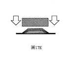
對於薄的塗層厚度,塗層逐漸變薄的該構造可能是足夠的。對於較厚塗層,可能有利的是在圖案(區域)302F上使用第二掩模(圖17E)並且在反射圖案(區域)302F旁邊施加互補透明塗層398,如圖17F所示。應當注意,圖17E的掩模通常並非圖17D的掩模的精確反轉,因為其優選地在邊界周圍增加對應於拖尾區域的量(其可憑經驗確定)。For thin coating thicknesses, this configuration in which the coating is tapered may be sufficient. For thicker coatings, it may be advantageous to use a second mask (FIG. 17E) over the pattern (region) 302F and apply a complementary
應當理解,以上描述僅旨在用作示例,並且在所附申請專利範圍中限定的本發明的範圍內,許多其他實施方式是可能的。It should be understood that the above description is intended to serve as an example only and that many other embodiments are possible within the scope of the invention as defined in the appended claims.
220A1、220A2、220B1、220B2、220C:圖像220A1, 220A2, 220B1, 220B2, 220C: Image
224、226:小平面224, 226: facets
228:圓228: round
Claims (10)
Translated fromChineseApplications Claiming Priority (6)
| Application Number | Priority Date | Filing Date | Title |
|---|---|---|---|
| US202063069059P | 2020-08-23 | 2020-08-23 | |
| US63/069,059 | 2020-08-23 | ||
| US202063072174P | 2020-08-30 | 2020-08-30 | |
| US63/072,174 | 2020-08-30 | ||
| US202063076971P | 2020-09-11 | 2020-09-11 | |
| US63/076,971 | 2020-09-11 |
Publications (1)
| Publication Number | Publication Date |
|---|---|
| TW202215108Atrue TW202215108A (en) | 2022-04-16 |
Family
ID=80354786
Family Applications (1)
| Application Number | Title | Priority Date | Filing Date |
|---|---|---|---|
| TW110131127ATW202215108A (en) | 2020-08-23 | 2021-08-23 | Optical system |
Country Status (10)
| Country | Link |
|---|---|
| US (2) | US20220269098A1 (en) |
| EP (2) | EP4022382B1 (en) |
| JP (1) | JP2023538349A (en) |
| KR (1) | KR20230054841A (en) |
| CN (2) | CN118210141A (en) |
| AU (1) | AU2021331833A1 (en) |
| CA (1) | CA3190651A1 (en) |
| IL (1) | IL300754A (en) |
| TW (1) | TW202215108A (en) |
| WO (1) | WO2022044001A1 (en) |
Families Citing this family (10)
| Publication number | Priority date | Publication date | Assignee | Title |
|---|---|---|---|---|
| AU2021331833A1 (en)* | 2020-08-23 | 2023-03-09 | Lumus Ltd. | Optical system for two-dimensional expansion of an image reducing glints and ghosts from the waveguide |
| KR102436597B1 (en)* | 2020-09-09 | 2022-08-26 | 주식회사 레티널 | Optical device for augmented reality having optical structure arranged in straight line and manufacturing method for optical means |
| IL313871A (en) | 2022-01-07 | 2024-08-01 | Lumus Ltd | Optical system for directing an image for viewing |
| WO2024003754A2 (en)* | 2022-06-28 | 2024-01-04 | Lumus Ltd. | A novel near eye display optical system |
| DE102022207139B3 (en)* | 2022-07-13 | 2023-10-26 | VIAHOLO GmbH | Glasses display device for displaying a virtual image in a downwardly tapering, virtually expandable field of view of the glasses display device |
| WO2024038458A1 (en) | 2022-08-18 | 2024-02-22 | Lumus Ltd. | Image projector with polarizing catadioptric collimator |
| CN116661050B (en)* | 2023-07-24 | 2023-11-07 | 北京灵犀微光科技有限公司 | Optical waveguide device and near-to-eye display equipment |
| WO2025099718A1 (en)* | 2023-11-09 | 2025-05-15 | Lumus Ltd. | Optical systems having light-guide optical element and homogenizing arrangement |
| WO2025104737A1 (en)* | 2023-11-19 | 2025-05-22 | Lumus Ltd. | Lightguide-based display |
| CN118707728A (en)* | 2024-07-12 | 2024-09-27 | 北京灵犀微光科技有限公司 | A symmetrical pupil expansion device and near-eye display device |
Family Cites Families (233)
| Publication number | Priority date | Publication date | Assignee | Title |
|---|---|---|---|---|
| US2748659A (en) | 1951-02-26 | 1956-06-05 | Jenaer Glaswerk Schott & Gen | Light source, searchlight or the like for polarized light |
| US2886911A (en) | 1953-07-23 | 1959-05-19 | George K C Hardesty | Duo-panel edge illumination system |
| US2795069A (en) | 1956-02-07 | 1957-06-11 | George K C Hardesty | Laminated metal-plastic illuminable panel |
| US3491245A (en) | 1967-04-10 | 1970-01-20 | George K C Hardesty | Guided light display panel |
| DE2057827A1 (en) | 1969-11-24 | 1971-06-03 | Vickers Ltd | Optical arrangement for flattening the image field |
| US3626394A (en) | 1970-04-09 | 1971-12-07 | Magnavox Co | Magneto-optical system |
| US3667621A (en) | 1970-10-20 | 1972-06-06 | Wisconsin Foundry And Machine | Fluid power system for a self-contained unloading unit |
| US3737212A (en) | 1970-12-14 | 1973-06-05 | Gen Electric | Diffraction optics head up display |
| GB1377627A (en) | 1971-09-01 | 1974-12-18 | Rank Organisation Ltd | Beam splitting prisms |
| US3857109A (en) | 1973-11-21 | 1974-12-24 | Us Navy | Longitudinally-pumped two-wavelength lasers |
| US3873209A (en) | 1973-12-10 | 1975-03-25 | Bell Telephone Labor Inc | Measurement of thin films by optical waveguiding technique |
| FR2295436A1 (en) | 1974-12-16 | 1976-07-16 | Radiotechnique Compelec | DIRECTIVE COUPLING DEVICE FOR MULTIMODES OPTICAL FIBERS |
| US3940204A (en) | 1975-01-23 | 1976-02-24 | Hughes Aircraft Company | Optical display systems utilizing holographic lenses |
| US4084883A (en) | 1977-02-28 | 1978-04-18 | The University Of Rochester | Reflective polarization retarder and laser apparatus utilizing same |
| DE3000402A1 (en) | 1979-01-19 | 1980-07-31 | Smiths Industries Ltd | DISPLAY DEVICE |
| US4241382A (en) | 1979-03-23 | 1980-12-23 | Maurice Daniel | Fiber optics illuminator |
| US4331387A (en) | 1980-07-03 | 1982-05-25 | Westinghouse Electric Corp. | Electro-optical modulator for randomly polarized light |
| DE3266408D1 (en) | 1981-10-14 | 1985-10-24 | Gec Avionics | Optical arrangements for head-up displays and night vision goggles |
| US4516828A (en) | 1982-05-03 | 1985-05-14 | General Motors Corporation | Duplex communication on a single optical fiber |
| FR2562273B1 (en) | 1984-03-27 | 1986-08-08 | France Etat Armement | DEVICE FOR OBSERVING THROUGH A WALL IN TWO OPPOSITE DIRECTIONS |
| US4715684A (en) | 1984-06-20 | 1987-12-29 | Hughes Aircraft Company | Optical system for three color liquid crystal light valve image projection system |
| US4711512A (en) | 1985-07-12 | 1987-12-08 | Environmental Research Institute Of Michigan | Compact head-up display |
| US4805988A (en) | 1987-07-24 | 1989-02-21 | Nelson Dones | Personal video viewing device |
| US4798448A (en) | 1988-02-16 | 1989-01-17 | General Electric Company | High efficiency illumination system for display devices |
| US4932743A (en) | 1988-04-18 | 1990-06-12 | Ricoh Company, Ltd. | Optical waveguide device |
| EP0365406B1 (en) | 1988-10-21 | 1993-09-29 | Thomson-Csf | Optical collimating system for a helmet visual |
| CN1043203A (en) | 1988-12-02 | 1990-06-20 | 三井石油化学工业株式会社 | Light output control method and device thereof |
| US4978952A (en) | 1989-02-24 | 1990-12-18 | Collimated Displays Incorporated | Flat screen color video display |
| FR2647556B1 (en) | 1989-05-23 | 1993-10-29 | Thomson Csf | OPTICAL DEVICE FOR INTRODUCING A COLLIMATED IMAGE INTO THE VISUAL FIELD OF AN OBSERVER AND HELMET COMPRISING AT LEAST ONE SUCH DEVICE |
| US5157526A (en) | 1990-07-06 | 1992-10-20 | Hitachi, Ltd. | Unabsorbing type polarizer, method for manufacturing the same, polarized light source using the same, and apparatus for liquid crystal display using the same |
| US5096520A (en) | 1990-08-01 | 1992-03-17 | Faris Sades M | Method for producing high efficiency polarizing filters |
| US5751480A (en) | 1991-04-09 | 1998-05-12 | Canon Kabushiki Kaisha | Plate-like polarizing element, a polarizing conversion unit provided with the element, and a projector provided with the unit |
| FR2683918B1 (en) | 1991-11-19 | 1994-09-09 | Thomson Csf | MATERIAL CONSTITUTING A RIFLE SCOPE AND WEAPON USING THE SAME. |
| US5367399A (en) | 1992-02-13 | 1994-11-22 | Holotek Ltd. | Rotationally symmetric dual reflection optical beam scanner and system using same |
| US5301067A (en) | 1992-05-06 | 1994-04-05 | Plx Inc. | High accuracy periscope assembly |
| US5231642A (en) | 1992-05-08 | 1993-07-27 | Spectra Diode Laboratories, Inc. | Semiconductor ring and folded cavity lasers |
| US5369415A (en) | 1992-06-29 | 1994-11-29 | Motorola, Inc. | Direct retinal scan display with planar imager |
| WO1994004892A1 (en) | 1992-08-13 | 1994-03-03 | Maechler Meinrad | Spectroscopic systems for the analysis of small and very small quantities of substances |
| US6144347A (en) | 1992-10-09 | 2000-11-07 | Sony Corporation | Head-mounted image display apparatus |
| US5537173A (en) | 1992-10-23 | 1996-07-16 | Olympus Optical Co., Ltd. | Film winding detecting means for a camera including control means for controlling proper and accurate winding and rewinding of a film |
| DE69432526T2 (en) | 1993-02-26 | 2004-04-01 | Yeda Research And Development Co., Ltd. | OPTICAL HOLOGRAPHIC DEVICES |
| US5555329A (en) | 1993-11-05 | 1996-09-10 | Alliesignal Inc. | Light directing optical structure |
| JPH07199236A (en) | 1993-12-28 | 1995-08-04 | Fujitsu Ltd | Optical switch and optical distributor |
| JPH08114765A (en) | 1994-10-15 | 1996-05-07 | Fujitsu Ltd | Polarization separation / conversion device, polarized illumination device and projection type display device using the same |
| US5650873A (en) | 1995-01-30 | 1997-07-22 | Lockheed Missiles & Space Company, Inc. | Micropolarization apparatus |
| GB9521210D0 (en) | 1995-10-17 | 1996-08-28 | Barr & Stroud Ltd | Display system |
| US5829854A (en) | 1996-09-26 | 1998-11-03 | Raychem Corporation | Angled color dispersement and recombination prism |
| US6204974B1 (en) | 1996-10-08 | 2001-03-20 | The Microoptical Corporation | Compact image display system for eyeglasses or other head-borne frames |
| JPH10133055A (en) | 1996-10-31 | 1998-05-22 | Sharp Corp | Photocoupler and its production |
| US5919601A (en) | 1996-11-12 | 1999-07-06 | Kodak Polychrome Graphics, Llc | Radiation-sensitive compositions and printing plates |
| US5724163A (en) | 1996-11-12 | 1998-03-03 | Yariv Ben-Yehuda | Optical system for alternative or simultaneous direction of light originating from two scenes to the eye of a viewer |
| JPH10160961A (en) | 1996-12-03 | 1998-06-19 | Mitsubishi Gas Chem Co Inc | Optical element |
| US5883684A (en) | 1997-06-19 | 1999-03-16 | Three-Five Systems, Inc. | Diffusively reflecting shield optically, coupled to backlit lightguide, containing LED's completely surrounded by the shield |
| US5896232A (en) | 1997-08-07 | 1999-04-20 | International Business Machines Corporation | Highly efficient and compact frontlighting for polarization-based reflection light valves |
| US6091548A (en) | 1997-10-01 | 2000-07-18 | Raytheon Company | Optical system with two-stage aberration correction |
| EP1068548B1 (en)* | 1998-04-02 | 2003-11-12 | Elop Electro-Optics Industries Ltd. | Holographic optical devices |
| US20030063042A1 (en) | 1999-07-29 | 2003-04-03 | Asher A. Friesem | Electronic utility devices incorporating a compact virtual image display |
| CA2386856A1 (en) | 1999-10-14 | 2001-04-19 | Stratos Product Development Llc | Virtual imaging system |
| IL136248A (en) | 2000-05-21 | 2004-08-31 | Elop Electrooptics Ind Ltd | System and method for varying the transmittance of light through a media |
| ATE473464T1 (en) | 2000-06-05 | 2010-07-15 | Lumus Ltd | OPTICAL BEAM EXPANDER WITH SUBSTRATE LIGHT WAVE GUIDE |
| KR100514011B1 (en) | 2000-07-24 | 2005-09-13 | 미츠비시 레이온 가부시키가이샤 | Surface illuminant device and prism sheet used therefor |
| KR100388819B1 (en) | 2000-07-31 | 2003-06-25 | 주식회사 대양이앤씨 | Optical System for Head Mount Display |
| US6490104B1 (en) | 2000-09-15 | 2002-12-03 | Three-Five Systems, Inc. | Illumination system for a micro display |
| US6542307B2 (en) | 2000-10-20 | 2003-04-01 | Three-Five Systems, Inc. | Compact near-eye illumination system |
| US6626906B1 (en) | 2000-10-23 | 2003-09-30 | Sdgi Holdings, Inc. | Multi-planar adjustable connector |
| KR100813943B1 (en)* | 2001-04-30 | 2008-03-14 | 삼성전자주식회사 | Composite Reflective Prism and Optical Pick-up Device |
| US6690513B2 (en) | 2001-07-03 | 2004-02-10 | Jds Uniphase Corporation | Rhomb interleaver |
| US6791760B2 (en) | 2001-07-24 | 2004-09-14 | Itt Manufacturing Enterprises, Inc. | Planar diffractive relay |
| EP1433160A1 (en) | 2001-09-07 | 2004-06-30 | The Microoptical Corporation | Light weight, compact, remountable face-supported electronic display |
| JP2003140081A (en) | 2001-11-06 | 2003-05-14 | Nikon Corp | Hologram combiner optical system |
| FR2834799B1 (en) | 2002-01-11 | 2004-04-16 | Essilor Int | OPHTHALMIC LENS WITH PROJECTION INSERT |
| IL148804A (en) | 2002-03-21 | 2007-02-11 | Yaacov Amitai | Optical device |
| DE10216169A1 (en) | 2002-04-12 | 2003-10-30 | Zeiss Carl Jena Gmbh | Arrangement for the polarization of light |
| ITTO20020625A1 (en)* | 2002-07-17 | 2004-01-19 | Fiat Ricerche | LIGHT GUIDE FOR "HEAD-MOUNTED" OR "HEAD-UP" TYPE DISPLAY DEVICES |
| EP1418459A1 (en) | 2002-11-08 | 2004-05-12 | 3M Innovative Properties Company | Optical device comprising cubo-octahedral polyhedron as light flux splitter or light diffusing element |
| US20050174641A1 (en) | 2002-11-26 | 2005-08-11 | Jds Uniphase Corporation | Polarization conversion light integrator |
| US7206133B2 (en) | 2003-05-22 | 2007-04-17 | Optical Research Associates | Light distribution apparatus and methods for illuminating optical systems |
| US20050017465A1 (en) | 2003-07-24 | 2005-01-27 | Bergstrom Skegs, Inc. | Wear rod for a snowmobile ski |
| IL157837A (en) | 2003-09-10 | 2012-12-31 | Yaakov Amitai | Substrate-guided optical device particularly for three-dimensional displays |
| IL157838A (en) | 2003-09-10 | 2013-05-30 | Yaakov Amitai | High brightness optical device |
| KR20050037085A (en) | 2003-10-17 | 2005-04-21 | 삼성전자주식회사 | Light tunnel, illuminating device and projector adopting the same |
| US7101063B2 (en) | 2004-02-05 | 2006-09-05 | Hewlett-Packard Development Company, L.P. | Systems and methods for integrating light |
| JP4218553B2 (en) | 2004-03-08 | 2009-02-04 | ソニー株式会社 | Image display device |
| EP1748305A4 (en) | 2004-05-17 | 2009-01-14 | Nikon Corp | Optical element, combiner optical system, and image display unit |
| TWI282017B (en) | 2004-05-28 | 2007-06-01 | Epistar Corp | Planar light device |
| IL162572A (en) | 2004-06-17 | 2013-02-28 | Lumus Ltd | High brightness optical device |
| IL162573A (en) | 2004-06-17 | 2013-05-30 | Lumus Ltd | Substrate-guided optical device with very wide aperture |
| US7778508B2 (en) | 2004-12-06 | 2010-08-17 | Nikon Corporation | Image display optical system, image display unit, illuminating optical system, and liquid crystal display unit |
| US20060126181A1 (en) | 2004-12-13 | 2006-06-15 | Nokia Corporation | Method and system for beam expansion in a display device |
| JP2008533507A (en) | 2005-02-10 | 2008-08-21 | ラマス リミテッド | Substrate guiding optical device especially for vision enhancement optical system |
| US7724443B2 (en) | 2005-02-10 | 2010-05-25 | Lumus Ltd. | Substrate-guided optical device utilizing thin transparent layer |
| US10073264B2 (en) | 2007-08-03 | 2018-09-11 | Lumus Ltd. | Substrate-guide optical device |
| IL166799A (en) | 2005-02-10 | 2014-09-30 | Lumus Ltd | Substrate-guided optical device utilizing beam splitters |
| EP1848966A1 (en) | 2005-02-17 | 2007-10-31 | Lumus Ltd | Personal navigation system |
| US7405881B2 (en) | 2005-05-30 | 2008-07-29 | Konica Minolta Holdings, Inc. | Image display apparatus and head mount display |
| JP4655771B2 (en) | 2005-06-17 | 2011-03-23 | ソニー株式会社 | Optical device and virtual image display device |
| US20070002191A1 (en) | 2005-07-01 | 2007-01-04 | Seiko Epson Corporation | Projector |
| US20070007157A1 (en) | 2005-07-05 | 2007-01-11 | Buschmann Jeffrey P | Bottle-pack for light bulb |
| US9081178B2 (en) | 2005-09-07 | 2015-07-14 | Bae Systems Plc | Projection display for displaying an image to a viewer |
| US10261321B2 (en) | 2005-11-08 | 2019-04-16 | Lumus Ltd. | Polarizing optical system |
| IL171820A (en) | 2005-11-08 | 2014-04-30 | Lumus Ltd | Polarizing optical device for light coupling |
| IL173715A0 (en) | 2006-02-14 | 2007-03-08 | Lumus Ltd | Substrate-guided imaging lens |
| IL174170A (en) | 2006-03-08 | 2015-02-26 | Abraham Aharoni | Device and method for binocular alignment |
| IL177618A (en) | 2006-08-22 | 2015-02-26 | Lumus Ltd | Substrate- guided optical device |
| JP2010502192A (en) | 2006-08-31 | 2010-01-28 | アメリカ合衆国 | BORIS isoforms and methods for detecting and treating disease |
| US7826113B2 (en) | 2007-03-28 | 2010-11-02 | Konica Minolta Holdings, Inc. | Joined optical member, image display apparatus, and head-mounted display |
| US8643948B2 (en) | 2007-04-22 | 2014-02-04 | Lumus Ltd. | Collimating optical device and system |
| US8139944B2 (en) | 2007-05-08 | 2012-03-20 | The Boeing Company | Method and apparatus for clearing an optical channel |
| IL183637A (en) | 2007-06-04 | 2013-06-27 | Zvi Lapidot | Distributed head-mounted display |
| US7589901B2 (en) | 2007-07-10 | 2009-09-15 | Microvision, Inc. | Substrate-guided relays for use with scanned beam light sources |
| US8433199B2 (en) | 2008-03-18 | 2013-04-30 | Princeton University | System and method for nonlinear self-filtering via dynamical stochastic resonance |
| WO2009127849A1 (en)* | 2008-04-14 | 2009-10-22 | Bae Systems Plc | Improvements in or relating to waveguides |
| WO2010022101A2 (en) | 2008-08-19 | 2010-02-25 | Plextronics, Inc. | Organic light emitting diode lighting devices |
| US7949214B2 (en) | 2008-11-06 | 2011-05-24 | Microvision, Inc. | Substrate guided relay with pupil expanding input coupler |
| US20110194163A1 (en) | 2008-11-26 | 2011-08-11 | Konica Minolta Opto, Inc. | Image display device and head-mounted display |
| US8317352B2 (en) | 2008-12-11 | 2012-11-27 | Robert Saccomanno | Non-invasive injection of light into a transparent substrate, such as a window pane through its face |
| CN102356338B (en) | 2009-04-08 | 2015-03-11 | 国际商业机器公司 | Optical waveguide with embedded light-reflecting feature and method for fabricating the same |
| WO2010124028A2 (en) | 2009-04-21 | 2010-10-28 | Vasylyev Sergiy V | Light collection and illumination systems employing planar waveguide |
| US9335604B2 (en) | 2013-12-11 | 2016-05-10 | Milan Momcilo Popovich | Holographic waveguide display |
| US20100291489A1 (en) | 2009-05-15 | 2010-11-18 | Api Nanofabrication And Research Corp. | Exposure methods for forming patterned layers and apparatus for performing the same |
| JP5104823B2 (en) | 2009-07-29 | 2012-12-19 | 株式会社島津製作所 | Display device |
| US8870384B2 (en) | 2009-09-28 | 2014-10-28 | Nec Corporation | Projection display device having light source device with color synthesis unit |
| US8233204B1 (en) | 2009-09-30 | 2012-07-31 | Rockwell Collins, Inc. | Optical displays |
| EP2558893A4 (en) | 2010-04-16 | 2014-06-11 | Flex Lighting Ii Llc | TEACH COMPRISING A LIGHT GUIDE BASED ON A FILM |
| US9028123B2 (en) | 2010-04-16 | 2015-05-12 | Flex Lighting Ii, Llc | Display illumination device with a film-based lightguide having stacked incident surfaces |
| US8743464B1 (en) | 2010-11-03 | 2014-06-03 | Google Inc. | Waveguide with embedded mirrors |
| JP5645631B2 (en) | 2010-12-13 | 2014-12-24 | 三菱電機株式会社 | Wavelength monitor, optical module, and wavelength monitoring method |
| JP2012160813A (en) | 2011-01-31 | 2012-08-23 | Sony Corp | Image data transmission device, image data transmission method, image data reception device, and image data reception method |
| JP5720290B2 (en) | 2011-02-16 | 2015-05-20 | セイコーエプソン株式会社 | Virtual image display device |
| JP2012252091A (en) | 2011-06-01 | 2012-12-20 | Sony Corp | Display apparatus |
| US8760762B1 (en) | 2011-08-12 | 2014-06-24 | Google Inc. | Image waveguide utilizing two mirrored or polarized surfaces |
| US8548290B2 (en) | 2011-08-23 | 2013-10-01 | Vuzix Corporation | Dynamic apertured waveguide for near-eye display |
| CN206649211U (en) | 2017-02-24 | 2017-11-17 | 北京耐德佳显示技术有限公司 | A kind of nearly eye display device using Waveguide mode optical element |
| US8736963B2 (en) | 2012-03-21 | 2014-05-27 | Microsoft Corporation | Two-dimensional exit-pupil expansion |
| IL219907A (en) | 2012-05-21 | 2017-08-31 | Lumus Ltd | Head-mounted display eyeball tracker integrated system |
| US20130321432A1 (en) | 2012-06-01 | 2013-12-05 | QUALCOMM MEMES Technologies, Inc. | Light guide with embedded fresnel reflectors |
| CN115494654B (en) | 2012-06-11 | 2025-08-01 | 奇跃公司 | Multi-depth planar three-dimensional display using waveguide reflector array projector |
| US9671566B2 (en) | 2012-06-11 | 2017-06-06 | Magic Leap, Inc. | Planar waveguide apparatus with diffraction element(s) and system employing same |
| US8913324B2 (en) | 2012-08-07 | 2014-12-16 | Nokia Corporation | Display illumination light guide |
| FR2999301B1 (en) | 2012-12-12 | 2015-01-09 | Thales Sa | OPTICAL GUIDE OF COLLIMATE IMAGES WITH OPTICAL BEAM DEDOLDER AND OPTICAL DEVICE THEREFOR |
| US8947783B2 (en) | 2013-01-02 | 2015-02-03 | Google Inc. | Optical combiner for near-eye display |
| JP6065630B2 (en) | 2013-02-13 | 2017-01-25 | セイコーエプソン株式会社 | Virtual image display device |
| DE102013106392B4 (en) | 2013-06-19 | 2017-06-08 | Fraunhofer-Gesellschaft zur Förderung der angewandten Forschung e.V. | Process for producing an antireflection coating |
| US9630220B2 (en) | 2013-07-05 | 2017-04-25 | Juin-Ping KUAN | Air-wiping device opening and closing in one level plane |
| US10228242B2 (en) | 2013-07-12 | 2019-03-12 | Magic Leap, Inc. | Method and system for determining user input based on gesture |
| US20150081313A1 (en) | 2013-09-16 | 2015-03-19 | Sunedison Llc | Methods and systems for photovoltaic site installation, commissioining, and provisioning |
| JP6225657B2 (en)* | 2013-11-15 | 2017-11-08 | セイコーエプソン株式会社 | OPTICAL ELEMENT, IMAGE DISPLAY DEVICE, AND MANUFACTURING METHOD THEREOF |
| US9766463B2 (en) | 2014-01-21 | 2017-09-19 | Osterhout Group, Inc. | See-through computer display systems |
| US9395544B2 (en) | 2014-03-13 | 2016-07-19 | Google Inc. | Eyepiece with switchable reflector for head wearable display |
| CN108572449B (en) | 2014-03-31 | 2021-09-14 | 联想(北京)有限公司 | Display device and electronic apparatus |
| DE102014207490B3 (en) | 2014-04-17 | 2015-07-02 | Carl Zeiss Ag | Spectacle lens for a display device to be placed on the head of a user and an image-generating display device and display device with such a spectacle lens |
| IL232197B (en) | 2014-04-23 | 2018-04-30 | Lumus Ltd | Compact head-mounted display system |
| JP6096713B2 (en) | 2014-05-21 | 2017-03-15 | 株式会社東芝 | Display device |
| US9285591B1 (en) | 2014-08-29 | 2016-03-15 | Google Inc. | Compact architecture for near-to-eye display system |
| CN112925100B (en) | 2014-09-29 | 2023-10-31 | 奇跃公司 | Optical system |
| IL235642B (en) | 2014-11-11 | 2021-08-31 | Lumus Ltd | Compact head-mounted display system protected by a hyperfine structure |
| IL236490B (en) | 2014-12-25 | 2021-10-31 | Lumus Ltd | Optical component on a conductive substrate |
| IL236491B (en) | 2014-12-25 | 2020-11-30 | Lumus Ltd | A method for fabricating substrate-guided optical device |
| CN107430283A (en) | 2015-01-06 | 2017-12-01 | 伊奎蒂公司 | Head-mounted imaging device with optical coupling |
| CN104503087B (en) | 2015-01-25 | 2019-07-30 | 上海理湃光晶技术有限公司 | Polarize guide-lighting planar waveguide optical display device |
| US20160234485A1 (en) | 2015-02-09 | 2016-08-11 | Steven John Robbins | Display System |
| IL237337B (en) | 2015-02-19 | 2020-03-31 | Amitai Yaakov | Compact head-mounted display system having uniform image |
| JP2016177231A (en) | 2015-03-23 | 2016-10-06 | セイコーエプソン株式会社 | Light guide device, head-mounted display, and manufacturing method for light guide device |
| US10345594B2 (en) | 2015-12-18 | 2019-07-09 | Ostendo Technologies, Inc. | Systems and methods for augmented near-eye wearable displays |
| CN108700714A (en) | 2016-01-06 | 2018-10-23 | 伊奎蒂公司 | Head-mounted display with pivoting imaging light guide |
| FR3046850B1 (en)* | 2016-01-15 | 2018-01-26 | Universite De Strasbourg | IMPROVED OPTICAL GUIDE AND OPTICAL SYSTEM COMPRISING SUCH AN OPTICAL GUIDE |
| US10473933B2 (en) | 2016-02-19 | 2019-11-12 | Microsoft Technology Licensing, Llc | Waveguide pupil relay |
| CN107290816B (en) | 2016-03-30 | 2020-04-24 | 中强光电股份有限公司 | Optical waveguide element and head-mounted display device having the same |
| US20170343810A1 (en) | 2016-05-24 | 2017-11-30 | Osterhout Group, Inc. | Pre-assembled solid optical assembly for head worn computers |
| US20170293140A1 (en) | 2016-04-12 | 2017-10-12 | Ostendo Technologies, Inc. | Split Exit Pupil Heads-Up Display Systems and Methods |
| US9791703B1 (en) | 2016-04-13 | 2017-10-17 | Microsoft Technology Licensing, Llc | Waveguides with extended field of view |
| US10061124B2 (en) | 2016-04-29 | 2018-08-28 | Microsoft Technology Licensing, Llc | Robust architecture for large field of view components |
| JP6740366B2 (en) | 2016-05-18 | 2020-08-12 | ルーマス リミテッドLumus Ltd. | Head mount imaging device |
| US10663745B2 (en) | 2016-06-09 | 2020-05-26 | 3M Innovative Properties Company | Optical system |
| JP7166927B2 (en)* | 2016-06-20 | 2022-11-08 | アコニア ホログラフィックス、エルエルシー | pupil dilation |
| US20200192101A1 (en)* | 2016-06-20 | 2020-06-18 | Apple Inc. | Pupil expansion |
| WO2018065975A1 (en)* | 2016-10-09 | 2018-04-12 | Lumus Ltd | Aperture multiplier using a rectangular waveguide |
| KR20240160657A (en) | 2016-11-08 | 2024-11-11 | 루머스 리미티드 | Light-guide device with optical cutoff edge and corresponding production methods |
| EP3542213B1 (en) | 2016-11-18 | 2025-10-08 | Magic Leap, Inc. | Waveguide light multiplexer using crossed gratings |
| EP4152077A1 (en)* | 2016-11-30 | 2023-03-22 | Magic Leap, Inc. | Method and system for high resolution digitized display |
| DE212017000261U1 (en) | 2016-12-02 | 2019-08-05 | Lumus Ltd. | Optical system with compact collimator image projector |
| KR102296369B1 (en) | 2016-12-31 | 2021-09-01 | 루머스 리미티드 | Retinal Imaging-Based Eye Tracker with Light-Guiding Optics |
| WO2018127913A1 (en) | 2017-01-04 | 2018-07-12 | Lumus Ltd. | Optical system for near-eye displays |
| CN108445573B (en) | 2017-02-16 | 2023-06-30 | 中强光电股份有限公司 | Optical waveguide element and display device |
| CN108738358B (en) | 2017-02-22 | 2021-03-26 | 鲁姆斯有限公司 | Light guide optics |
| CA3053963A1 (en) | 2017-03-14 | 2018-09-20 | Magic Leap, Inc. | Waveguides with light absorbing films and processes for forming the same |
| CN106976811B (en) | 2017-03-16 | 2019-08-30 | 张俊强 | A kind of torque converter drive system and dynamic compaction machinery for dynamic compaction machinery |
| CN109416433B (en)* | 2017-03-22 | 2021-06-01 | 鲁姆斯有限公司 | Overlapping Reflector Construction |
| US10852543B2 (en) | 2017-03-28 | 2020-12-01 | Seiko Epson Corporation | Light guide device and display device |
| IL251645B (en) | 2017-04-06 | 2018-08-30 | Lumus Ltd | Light-guide optical element and method of its manufacture |
| JP6927295B2 (en) | 2017-05-18 | 2021-08-25 | ソニーグループ株式会社 | Information processing equipment, information processing methods and programs |
| JP2018205448A (en) | 2017-05-31 | 2018-12-27 | セイコーエプソン株式会社 | Display device and lighting device |
| CN107238928B (en) | 2017-06-09 | 2020-03-06 | 京东方科技集团股份有限公司 | an arrayed waveguide |
| CN109116556A (en) | 2017-06-23 | 2019-01-01 | 芋头科技(杭州)有限公司 | A kind of imaging display system |
| EP4215980A1 (en) | 2017-07-19 | 2023-07-26 | Lumus Ltd. | Lcos illumination via loe |
| FR3069420B1 (en) | 2017-07-31 | 2019-08-16 | Albea Services | CASE FOR COSMETIC PRODUCT |
| US10859833B2 (en) | 2017-08-18 | 2020-12-08 | Tipd, Llc | Waveguide image combiner for augmented reality displays |
| US11513352B2 (en) | 2017-09-29 | 2022-11-29 | Lumus Ltd. | Augmented reality display |
| WO2019079014A1 (en)* | 2017-10-16 | 2019-04-25 | Akonia Holographics Llc | Two-dimensional light homogenization |
| WO2019077614A1 (en) | 2017-10-22 | 2019-04-25 | Lumus Ltd. | ENHANCED REALITY DEVICE MOUNTED ON THE HEAD AND USING AN OPTICAL BENCH |
| WO2019102366A1 (en)* | 2017-11-21 | 2019-05-31 | Lumus Ltd. | Optical aperture expansion arrangement for near-eye displays |
| US20190170327A1 (en) | 2017-12-03 | 2019-06-06 | Lumus Ltd. | Optical illuminator device |
| IL275013B (en) | 2017-12-03 | 2022-08-01 | Lumus Ltd | Method and device for testing an optics device |
| CN111417883B (en) | 2017-12-03 | 2022-06-17 | 鲁姆斯有限公司 | Optical equipment alignment method |
| KR102704523B1 (en) | 2017-12-10 | 2024-09-06 | 루머스 리미티드 | Image projector |
| KR20200102408A (en) | 2018-01-02 | 2020-08-31 | 루머스 리미티드 | Augmented Reality Display with Active Alignment and Corresponding Method |
| US10506220B2 (en) | 2018-01-02 | 2019-12-10 | Lumus Ltd. | Augmented reality displays with active alignment and corresponding methods |
| US10551544B2 (en)* | 2018-01-21 | 2020-02-04 | Lumus Ltd. | Light-guide optical element with multiple-axis internal aperture expansion |
| US10942355B2 (en) | 2018-01-22 | 2021-03-09 | Facebook Technologies, Llc | Systems, devices, and methods for tiled multi-monochromatic displays |
| US11256004B2 (en) | 2018-03-20 | 2022-02-22 | Invensas Bonding Technologies, Inc. | Direct-bonded lamination for improved image clarity in optical devices |
| MY203244A (en) | 2018-04-08 | 2024-06-19 | Lumus Ltd | Optical sample characterization |
| KR102752134B1 (en) | 2018-05-14 | 2025-01-08 | 루머스 리미티드 | Projector configuration with sub-optical aperture for near-eye display and corresponding optical system |
| IL278511B2 (en) | 2018-05-17 | 2025-01-01 | Lumus Ltd | Near-eye display having overlapping projector assemblies |
| IL259518B2 (en) | 2018-05-22 | 2023-04-01 | Lumus Ltd | Optical system and method for improvement of light field uniformity |
| MX2020012512A (en) | 2018-05-23 | 2021-02-16 | Lumus Ltd | Optical system including light-guide optical element with partially-reflective internal surfaces. |
| TWM587757U (en) | 2018-05-27 | 2019-12-11 | 以色列商魯姆斯有限公司 | Substrate-guide based optical systems with field curvature effect |
| US11415812B2 (en) | 2018-06-26 | 2022-08-16 | Lumus Ltd. | Compact collimating optical device and system |
| EP3824335B1 (en) | 2018-07-16 | 2023-10-18 | Lumus Ltd. | Light-guide optical element employing polarized internal reflectors |
| CN112601993A (en) | 2018-08-26 | 2021-04-02 | 鲁姆斯有限公司 | Reflection suppression in near-eye displays |
| CN116184666A (en) | 2018-09-09 | 2023-05-30 | 鲁姆斯有限公司 | Optical system comprising a light-guiding optical element with two-dimensional expansion |
| US10725291B2 (en)* | 2018-10-15 | 2020-07-28 | Facebook Technologies, Llc | Waveguide including volume Bragg gratings |
| JP3226277U (en) | 2018-11-11 | 2020-05-14 | ルムス エルティーディー. | Near eye display with intermediate window |
| JP7255189B2 (en) | 2019-01-15 | 2023-04-11 | セイコーエプソン株式会社 | virtual image display |
| MX2021008808A (en)* | 2019-01-24 | 2021-08-24 | Lumus Ltd | Optical systems including loe with three stage expansion. |
| IL264551B2 (en)* | 2019-01-29 | 2024-09-01 | Oorym Optics Ltd | Highly efficient compact head-mounted display system having small input aperture |
| US10942320B2 (en)* | 2019-02-11 | 2021-03-09 | Facebook Technologies, Llc | Dispersion compensation for light coupling through slanted facet of optical waveguide |
| CN109613644B (en) | 2019-02-14 | 2020-08-11 | 京东方科技集团股份有限公司 | A light guide device and its manufacturing method, and a display device |
| CN216434536U (en) | 2019-04-04 | 2022-05-03 | 鲁姆斯有限公司 | Near-eye display |
| TW202127106A (en) | 2019-09-04 | 2021-07-16 | 以色列商魯姆斯有限公司 | Optical devices having dichroic beam combiners, optical devices for use with dichroic beam combiners, and methods of manufacture therefor |
| WO2021055278A2 (en) | 2019-09-19 | 2021-03-25 | Akalana Management Llc | Optical systems with reflective prism input couplers |
| US10962787B1 (en) | 2019-11-25 | 2021-03-30 | Shanghai North Ocean Photonics Co., Ltd. | Waveguide display device |
| AU2021331833A1 (en)* | 2020-08-23 | 2023-03-09 | Lumus Ltd. | Optical system for two-dimensional expansion of an image reducing glints and ghosts from the waveguide |
| JP2022039127A (en)* | 2020-08-28 | 2022-03-10 | 株式会社日立エルジーデータストレージ | Head-mounted display |
- 2021
- 2021-08-23AUAU2021331833Apatent/AU2021331833A1/enactivePending
- 2021-08-23CACA3190651Apatent/CA3190651A1/enactivePending
- 2021-08-23EPEP21860749.7Apatent/EP4022382B1/enactiveActive
- 2021-08-23USUS17/640,004patent/US20220269098A1/ennot_activeAbandoned
- 2021-08-23WOPCT/IL2021/051034patent/WO2022044001A1/ennot_activeCeased
- 2021-08-23KRKR1020237007164Apatent/KR20230054841A/enactivePending
- 2021-08-23TWTW110131127Apatent/TW202215108A/enunknown
- 2021-08-23EPEP23179261.5Apatent/EP4242709A3/enactivePending
- 2021-08-23ILIL300754Apatent/IL300754A/enunknown
- 2021-08-23CNCN202410235528.0Apatent/CN118210141A/enactivePending
- 2021-08-23CNCN202180005416.0Apatent/CN114514460A/enactivePending
- 2021-08-23JPJP2023511682Apatent/JP2023538349A/enactivePending
- 2023
- 2023-01-26USUS18/101,607patent/US12436400B2/enactiveActive
Also Published As
| Publication number | Publication date |
|---|---|
| EP4022382B1 (en) | 2023-10-25 |
| US20220269098A1 (en) | 2022-08-25 |
| EP4022382A1 (en) | 2022-07-06 |
| US12436400B2 (en) | 2025-10-07 |
| KR20230054841A (en) | 2023-04-25 |
| IL300754A (en) | 2023-04-01 |
| JP2023538349A (en) | 2023-09-07 |
| CA3190651A1 (en) | 2022-03-03 |
| CN114514460A (en) | 2022-05-17 |
| EP4242709A3 (en) | 2023-11-22 |
| EP4242709A2 (en) | 2023-09-13 |
| AU2021331833A1 (en) | 2023-03-09 |
| WO2022044001A1 (en) | 2022-03-03 |
| US20230168519A1 (en) | 2023-06-01 |
| AU2021331833A2 (en) | 2023-03-16 |
| EP4022382A4 (en) | 2023-03-01 |
| CN118210141A (en) | 2024-06-18 |
Similar Documents
| Publication | Publication Date | Title |
|---|---|---|
| TW202215108A (en) | Optical system | |
| JP7546988B2 (en) | Optical system including a light directing optical element with two-dimensional magnification - Patents.com | |
| TWI865343B (en) | Optical system including a light-guiding optical element having two-dimensional expansion | |
| TWI751262B (en) | Overlapping facets | |
| TWI883048B (en) | Image display system with beam multiplication | |
| CN114846384B (en) | Optical system comprising a light-guiding optical element with two-dimensional expansion | |
| TW202323933A (en) | Optical system for near-eye displays | |
| CN118605021A (en) | Optical system and method for manufacturing the same | |
| TWI868462B (en) | Display with stacked light-guide elements providing different parts of field of view | |
| CN118103755A (en) | Optical system for near-eye display | |
| TW202346963A (en) | Optical system for directing an image for viewing | |
| TW202512997A (en) | Light-guide optical elements with embedded beam splitter overlapping coupling-out region | |
| TW202514182A (en) | Optical system with dual reflector coupling-in to lightguide | |
| TW202530589A (en) | Image display system with beam multiplication |