TW202213740A - Methods of forming microelectronic devices, and related microelectronic devices, memory devices, electronic systems, and additional methods - Google Patents
Methods of forming microelectronic devices, and related microelectronic devices, memory devices, electronic systems, and additional methodsDownload PDFInfo
- Publication number
- TW202213740A TW202213740ATW110119678ATW110119678ATW202213740ATW 202213740 ATW202213740 ATW 202213740ATW 110119678 ATW110119678 ATW 110119678ATW 110119678 ATW110119678 ATW 110119678ATW 202213740 ATW202213740 ATW 202213740A
- Authority
- TW
- Taiwan
- Prior art keywords
- structures
- conductive
- microelectronic device
- forming
- openings
- Prior art date
Links
- 238000004377microelectronicMethods0.000titleclaimsabstractdescription228
- 238000000034methodMethods0.000titleclaimsabstractdescription147
- 239000000463materialSubstances0.000claimsabstractdescription253
- 238000002955isolationMethods0.000claimsabstractdescription103
- 239000004020conductorSubstances0.000claimsabstractdescription46
- 238000011049fillingMethods0.000claimsabstractdescription6
- 239000011810insulating materialSubstances0.000claimsdescription81
- 230000008569processEffects0.000claimsdescription72
- 125000006850spacer groupChemical group0.000claimsdescription52
- 150000004767nitridesChemical class0.000claimsdescription34
- 238000010276constructionMethods0.000claimsdescription31
- 239000003989dielectric materialSubstances0.000claimsdescription23
- 239000010949copperSubstances0.000claimsdescription16
- RYGMFSIKBFXOCR-UHFFFAOYSA-NCopperChemical compound[Cu]RYGMFSIKBFXOCR-UHFFFAOYSA-N0.000claimsdescription5
- 229910052802copperInorganic materials0.000claimsdescription5
- 230000008878couplingEffects0.000claimsdescription4
- 238000010168coupling processMethods0.000claimsdescription4
- 238000005859coupling reactionMethods0.000claimsdescription4
- 229910052751metalInorganic materials0.000description51
- 239000002184metalSubstances0.000description51
- 239000004065semiconductorSubstances0.000description30
- VYPSYNLAJGMNEJ-UHFFFAOYSA-NSilicium dioxideChemical compoundO=[Si]=OVYPSYNLAJGMNEJ-UHFFFAOYSA-N0.000description25
- 229910045601alloyInorganic materials0.000description21
- 239000000956alloySubstances0.000description21
- 239000000203mixtureSubstances0.000description21
- 229910052814silicon oxideInorganic materials0.000description12
- 239000011521glassSubstances0.000description11
- 229910044991metal oxideInorganic materials0.000description11
- 150000004706metal oxidesChemical class0.000description11
- 238000012545processingMethods0.000description11
- 229910021332silicideInorganic materials0.000description10
- 229910052710siliconInorganic materials0.000description10
- XUIMIQQOPSSXEZ-UHFFFAOYSA-NSiliconChemical compound[Si]XUIMIQQOPSSXEZ-UHFFFAOYSA-N0.000description9
- 239000002019doping agentSubstances0.000description9
- 229910021420polycrystalline siliconInorganic materials0.000description9
- 239000010703siliconSubstances0.000description9
- 238000000231atomic layer depositionMethods0.000description8
- 238000005137deposition processMethods0.000description8
- 238000005530etchingMethods0.000description8
- PXHVJJICTQNCMI-UHFFFAOYSA-NNickelChemical compound[Ni]PXHVJJICTQNCMI-UHFFFAOYSA-N0.000description7
- 238000003491arrayMethods0.000description7
- 238000004891communicationMethods0.000description7
- 238000004519manufacturing processMethods0.000description7
- 238000005240physical vapour depositionMethods0.000description7
- 235000012239silicon dioxideNutrition0.000description7
- 229910020286SiOxNyInorganic materials0.000description6
- 239000005380borophosphosilicate glassSubstances0.000description6
- 229920005591polysiliconPolymers0.000description6
- FVBUAEGBCNSCDD-UHFFFAOYSA-Nsilicide(4-)Chemical compound[Si-4]FVBUAEGBCNSCDD-UHFFFAOYSA-N0.000description6
- 239000000377silicon dioxideSubstances0.000description6
- LIVNPJMFVYWSIS-UHFFFAOYSA-Nsilicon monoxideChemical compound[Si-]#[O+]LIVNPJMFVYWSIS-UHFFFAOYSA-N0.000description6
- XEEYBQQBJWHFJM-UHFFFAOYSA-NIronChemical compound[Fe]XEEYBQQBJWHFJM-UHFFFAOYSA-N0.000description5
- 229910004304SiNyInorganic materials0.000description5
- 229910000577Silicon-germaniumInorganic materials0.000description5
- 239000005388borosilicate glassSubstances0.000description5
- 229910052681coesiteInorganic materials0.000description5
- 229910052906cristobaliteInorganic materials0.000description5
- 238000007667floatingMethods0.000description5
- 229940104869fluorosilicateDrugs0.000description5
- CPLXHLVBOLITMK-UHFFFAOYSA-Nmagnesium oxideInorganic materials[Mg]=OCPLXHLVBOLITMK-UHFFFAOYSA-N0.000description5
- HBMJWWWQQXIZIP-UHFFFAOYSA-Nsilicon carbideChemical compound[Si+]#[C-]HBMJWWWQQXIZIP-UHFFFAOYSA-N0.000description5
- 229910010271silicon carbideInorganic materials0.000description5
- 229910052682stishoviteInorganic materials0.000description5
- 239000000758substrateSubstances0.000description5
- 229910052905tridymiteInorganic materials0.000description5
- KRHYYFGTRYWZRS-UHFFFAOYSA-NFluoraneChemical compoundFKRHYYFGTRYWZRS-UHFFFAOYSA-N0.000description4
- 229910002601GaNInorganic materials0.000description4
- LEVVHYCKPQWKOP-UHFFFAOYSA-N[Si].[Ge]Chemical compound[Si].[Ge]LEVVHYCKPQWKOP-UHFFFAOYSA-N0.000description4
- 230000015572biosynthetic processEffects0.000description4
- 150000001875compoundsChemical class0.000description4
- 150000001247metal acetylidesChemical class0.000description4
- 150000002739metalsChemical class0.000description4
- 229910021421monocrystalline siliconInorganic materials0.000description4
- 229910052759nickelInorganic materials0.000description4
- 238000001020plasma etchingMethods0.000description4
- 238000000623plasma-assisted chemical vapour depositionMethods0.000description4
- 239000011148porous materialSubstances0.000description4
- 230000008439repair processEffects0.000description4
- 239000010936titaniumSubstances0.000description4
- 229910052721tungstenInorganic materials0.000description4
- 239000010937tungstenSubstances0.000description4
- 229910017107AlOxInorganic materials0.000description3
- JMASRVWKEDWRBT-UHFFFAOYSA-NGallium nitrideChemical compound[Ga]#NJMASRVWKEDWRBT-UHFFFAOYSA-N0.000description3
- 229910052581Si3N4Inorganic materials0.000description3
- 229910003087TiOxInorganic materials0.000description3
- GWEVSGVZZGPLCZ-UHFFFAOYSA-NTitan oxideChemical compoundO=[Ti]=OGWEVSGVZZGPLCZ-UHFFFAOYSA-N0.000description3
- 229910052782aluminiumInorganic materials0.000description3
- 230000008859changeEffects0.000description3
- 229910052732germaniumInorganic materials0.000description3
- GNPVGFCGXDBREM-UHFFFAOYSA-Ngermanium atomChemical compound[Ge]GNPVGFCGXDBREM-UHFFFAOYSA-N0.000description3
- 229910052742ironInorganic materials0.000description3
- 239000000395magnesium oxideSubstances0.000description3
- 239000010955niobiumSubstances0.000description3
- 239000005360phosphosilicate glassSubstances0.000description3
- BASFCYQUMIYNBI-UHFFFAOYSA-NplatinumChemical compound[Pt]BASFCYQUMIYNBI-UHFFFAOYSA-N0.000description3
- 239000000126substanceSubstances0.000description3
- HLLICFJUWSZHRJ-UHFFFAOYSA-NtioxidazoleChemical compoundCCCOC1=CC=C2N=C(NC(=O)OC)SC2=C1HLLICFJUWSZHRJ-UHFFFAOYSA-N0.000description3
- OGIDPMRJRNCKJF-UHFFFAOYSA-Ntitanium oxideInorganic materials[Ti]=OOGIDPMRJRNCKJF-UHFFFAOYSA-N0.000description3
- JBRZTFJDHDCESZ-UHFFFAOYSA-NAsGaChemical compound[As]#[Ga]JBRZTFJDHDCESZ-UHFFFAOYSA-N0.000description2
- 229910001218Gallium arsenideInorganic materials0.000description2
- GPXJNWSHGFTCBW-UHFFFAOYSA-NIndium phosphideChemical compound[In]#PGPXJNWSHGFTCBW-UHFFFAOYSA-N0.000description2
- WFERVLWLPNZDOV-UHFFFAOYSA-NO[Si](O)(O)OP(=O)=OChemical compoundO[Si](O)(O)OP(=O)=OWFERVLWLPNZDOV-UHFFFAOYSA-N0.000description2
- KDLHZDBZIXYQEI-UHFFFAOYSA-NPalladiumChemical compound[Pd]KDLHZDBZIXYQEI-UHFFFAOYSA-N0.000description2
- MCMNRKCIXSYSNV-UHFFFAOYSA-NZirconium dioxideChemical compoundO=[Zr]=OMCMNRKCIXSYSNV-UHFFFAOYSA-N0.000description2
- LPQOADBMXVRBNX-UHFFFAOYSA-Nac1ldcw0Chemical compoundCl.C1CN(C)CCN1C1=C(F)C=C2C(=O)C(C(O)=O)=CN3CCSC1=C32LPQOADBMXVRBNX-UHFFFAOYSA-N0.000description2
- 230000009471actionEffects0.000description2
- 229910003481amorphous carbonInorganic materials0.000description2
- 239000011651chromiumSubstances0.000description2
- 239000011248coating agentSubstances0.000description2
- 238000000576coating methodMethods0.000description2
- 238000007796conventional methodMethods0.000description2
- 238000013461designMethods0.000description2
- 238000010586diagramMethods0.000description2
- 238000001312dry etchingMethods0.000description2
- 239000010931goldSubstances0.000description2
- 229910052735hafniumInorganic materials0.000description2
- 229910052738indiumInorganic materials0.000description2
- 238000009413insulationMethods0.000description2
- 239000012774insulation materialSubstances0.000description2
- 238000010884ion-beam techniqueMethods0.000description2
- 239000011777magnesiumSubstances0.000description2
- 239000007769metal materialSubstances0.000description2
- 238000012986modificationMethods0.000description2
- 230000004048modificationEffects0.000description2
- 229910003465moissaniteInorganic materials0.000description2
- QPJSUIGXIBEQAC-UHFFFAOYSA-Nn-(2,4-dichloro-5-propan-2-yloxyphenyl)acetamideChemical compoundCC(C)OC1=CC(NC(C)=O)=C(Cl)C=C1ClQPJSUIGXIBEQAC-UHFFFAOYSA-N0.000description2
- 229910052758niobiumInorganic materials0.000description2
- TWNQGVIAIRXVLR-UHFFFAOYSA-Noxo(oxoalumanyloxy)alumaneChemical compoundO=[Al]O[Al]=OTWNQGVIAIRXVLR-UHFFFAOYSA-N0.000description2
- 230000009467reductionEffects0.000description2
- 239000010948rhodiumSubstances0.000description2
- 239000002210silicon-based materialSubstances0.000description2
- 238000004528spin coatingMethods0.000description2
- 238000003860storageMethods0.000description2
- 229910052715tantalumInorganic materials0.000description2
- GUVRBAGPIYLISA-UHFFFAOYSA-Ntantalum atomChemical compound[Ta]GUVRBAGPIYLISA-UHFFFAOYSA-N0.000description2
- 238000012360testing methodMethods0.000description2
- 229910052719titaniumInorganic materials0.000description2
- WFKWXMTUELFFGS-UHFFFAOYSA-NtungstenChemical compound[W]WFKWXMTUELFFGS-UHFFFAOYSA-N0.000description2
- WQJQOUPTWCFRMM-UHFFFAOYSA-Ntungsten disilicideChemical compound[Si]#[W]#[Si]WQJQOUPTWCFRMM-UHFFFAOYSA-N0.000description2
- -1tungsten nitrideChemical class0.000description2
- 229910021342tungsten silicideInorganic materials0.000description2
- 230000000007visual effectEffects0.000description2
- 229910018072Al 2 O 3Inorganic materials0.000description1
- PIGFYZPCRLYGLF-UHFFFAOYSA-NAluminum nitrideChemical compound[Al]#NPIGFYZPCRLYGLF-UHFFFAOYSA-N0.000description1
- VYZAMTAEIAYCRO-UHFFFAOYSA-NChromiumChemical compound[Cr]VYZAMTAEIAYCRO-UHFFFAOYSA-N0.000description1
- 229910005540GaPInorganic materials0.000description1
- 229910001209Low-carbon steelInorganic materials0.000description1
- FYYHWMGAXLPEAU-UHFFFAOYSA-NMagnesiumChemical compound[Mg]FYYHWMGAXLPEAU-UHFFFAOYSA-N0.000description1
- ZOKXTWBITQBERF-UHFFFAOYSA-NMolybdenumChemical compound[Mo]ZOKXTWBITQBERF-UHFFFAOYSA-N0.000description1
- KJTLSVCANCCWHF-UHFFFAOYSA-NRutheniumChemical compound[Ru]KJTLSVCANCCWHF-UHFFFAOYSA-N0.000description1
- 229910004298SiO 2Inorganic materials0.000description1
- BQCADISMDOOEFD-UHFFFAOYSA-NSilverChemical compound[Ag]BQCADISMDOOEFD-UHFFFAOYSA-N0.000description1
- 229910000831SteelInorganic materials0.000description1
- RTAQQCXQSZGOHL-UHFFFAOYSA-NTitaniumChemical compound[Ti]RTAQQCXQSZGOHL-UHFFFAOYSA-N0.000description1
- 239000002253acidSubstances0.000description1
- 230000004913activationEffects0.000description1
- XAGFODPZIPBFFR-UHFFFAOYSA-NaluminiumChemical compound[Al]XAGFODPZIPBFFR-UHFFFAOYSA-N0.000description1
- 239000005354aluminosilicate glassSubstances0.000description1
- RNQKDQAVIXDKAG-UHFFFAOYSA-Naluminum galliumChemical compound[Al].[Ga]RNQKDQAVIXDKAG-UHFFFAOYSA-N0.000description1
- 238000000137annealingMethods0.000description1
- 230000004888barrier functionEffects0.000description1
- 230000008901benefitEffects0.000description1
- 239000000872bufferSubstances0.000description1
- 230000001413cellular effectEffects0.000description1
- 229910010293ceramic materialInorganic materials0.000description1
- 239000003795chemical substances by applicationSubstances0.000description1
- 238000005229chemical vapour depositionMethods0.000description1
- 229910052804chromiumInorganic materials0.000description1
- 229910017052cobaltInorganic materials0.000description1
- 239000010941cobaltSubstances0.000description1
- GUTLYIVDDKVIGB-UHFFFAOYSA-Ncobalt atomChemical compound[Co]GUTLYIVDDKVIGB-UHFFFAOYSA-N0.000description1
- 230000000295complement effectEffects0.000description1
- 238000012937correctionMethods0.000description1
- 239000013078crystalSubstances0.000description1
- 238000000151depositionMethods0.000description1
- 239000012777electrically insulating materialSubstances0.000description1
- HZXMRANICFIONG-UHFFFAOYSA-Ngallium phosphideChemical compound[Ga]#PHZXMRANICFIONG-UHFFFAOYSA-N0.000description1
- PCHJSUWPFVWCPO-UHFFFAOYSA-NgoldChemical compound[Au]PCHJSUWPFVWCPO-UHFFFAOYSA-N0.000description1
- 229910052737goldInorganic materials0.000description1
- 238000000227grindingMethods0.000description1
- VBJZVLUMGGDVMO-UHFFFAOYSA-Nhafnium atomChemical compound[Hf]VBJZVLUMGGDVMO-UHFFFAOYSA-N0.000description1
- 229910000449hafnium oxideInorganic materials0.000description1
- WIHZLLGSGQNAGK-UHFFFAOYSA-Nhafnium(4+);oxygen(2-)Chemical compound[O-2].[O-2].[Hf+4]WIHZLLGSGQNAGK-UHFFFAOYSA-N0.000description1
- 230000006872improvementEffects0.000description1
- 238000011065in-situ storageMethods0.000description1
- APFVFJFRJDLVQX-UHFFFAOYSA-Nindium atomChemical compound[In]APFVFJFRJDLVQX-UHFFFAOYSA-N0.000description1
- 239000012212insulatorSubstances0.000description1
- 230000010354integrationEffects0.000description1
- 229910052741iridiumInorganic materials0.000description1
- GKOZUEZYRPOHIO-UHFFFAOYSA-Niridium atomChemical compound[Ir]GKOZUEZYRPOHIO-UHFFFAOYSA-N0.000description1
- 229910052749magnesiumInorganic materials0.000description1
- AXZKOIWUVFPNLO-UHFFFAOYSA-Nmagnesium;oxygen(2-)Chemical compound[O-2].[Mg+2]AXZKOIWUVFPNLO-UHFFFAOYSA-N0.000description1
- 230000000873masking effectEffects0.000description1
- 229910052750molybdenumInorganic materials0.000description1
- 239000011733molybdenumSubstances0.000description1
- GUCVJGMIXFAOAE-UHFFFAOYSA-Nniobium atomChemical compound[Nb]GUCVJGMIXFAOAE-UHFFFAOYSA-N0.000description1
- 229910000484niobium oxideInorganic materials0.000description1
- URLJKFSTXLNXLG-UHFFFAOYSA-Nniobium(5+);oxygen(2-)Chemical compound[O-2].[O-2].[O-2].[O-2].[O-2].[Nb+5].[Nb+5]URLJKFSTXLNXLG-UHFFFAOYSA-N0.000description1
- 229910052762osmiumInorganic materials0.000description1
- SYQBFIAQOQZEGI-UHFFFAOYSA-Nosmium atomChemical compound[Os]SYQBFIAQOQZEGI-UHFFFAOYSA-N0.000description1
- BPUBBGLMJRNUCC-UHFFFAOYSA-Noxygen(2-);tantalum(5+)Chemical compound[O-2].[O-2].[O-2].[O-2].[O-2].[Ta+5].[Ta+5]BPUBBGLMJRNUCC-UHFFFAOYSA-N0.000description1
- 238000012856packingMethods0.000description1
- 229910052763palladiumInorganic materials0.000description1
- 230000003071parasitic effectEffects0.000description1
- 238000000059patterningMethods0.000description1
- 238000000206photolithographyMethods0.000description1
- 229910052697platinumInorganic materials0.000description1
- 238000007517polishing processMethods0.000description1
- 239000010453quartzSubstances0.000description1
- 229910052703rhodiumInorganic materials0.000description1
- MHOVAHRLVXNVSD-UHFFFAOYSA-Nrhodium atomChemical compound[Rh]MHOVAHRLVXNVSD-UHFFFAOYSA-N0.000description1
- 229910052707rutheniumInorganic materials0.000description1
- 150000003839saltsChemical class0.000description1
- 229910052594sapphireInorganic materials0.000description1
- 239000010980sapphireSubstances0.000description1
- VSZWPYCFIRKVQL-UHFFFAOYSA-Nselanylidenegallium;seleniumChemical compound[Se].[Se]=[Ga].[Se]=[Ga]VSZWPYCFIRKVQL-UHFFFAOYSA-N0.000description1
- 238000000926separation methodMethods0.000description1
- 239000005368silicate glassSubstances0.000description1
- 150000003376siliconChemical class0.000description1
- HQVNEWCFYHHQES-UHFFFAOYSA-Nsilicon nitrideChemical compoundN12[Si]34N5[Si]62N3[Si]51N64HQVNEWCFYHHQES-UHFFFAOYSA-N0.000description1
- 229910052709silverInorganic materials0.000description1
- 239000004332silverSubstances0.000description1
- 239000005361soda-lime glassSubstances0.000description1
- 238000004544sputter depositionMethods0.000description1
- 238000000992sputter etchingMethods0.000description1
- 229910001220stainless steelInorganic materials0.000description1
- 239000010935stainless steelSubstances0.000description1
- 239000010959steelSubstances0.000description1
- 229910001936tantalum oxideInorganic materials0.000description1
- 238000012546transferMethods0.000description1
- LEONUFNNVUYDNQ-UHFFFAOYSA-Nvanadium atomChemical compound[V]LEONUFNNVUYDNQ-UHFFFAOYSA-N0.000description1
- 239000012808vapor phaseSubstances0.000description1
- 238000001039wet etchingMethods0.000description1
Images


Classifications
- H—ELECTRICITY
- H01—ELECTRIC ELEMENTS
- H01L—SEMICONDUCTOR DEVICES NOT COVERED BY CLASS H10
- H01L21/00—Processes or apparatus adapted for the manufacture or treatment of semiconductor or solid state devices or of parts thereof
- H01L21/70—Manufacture or treatment of devices consisting of a plurality of solid state components formed in or on a common substrate or of parts thereof; Manufacture of integrated circuit devices or of parts thereof
- H01L21/71—Manufacture of specific parts of devices defined in group H01L21/70
- H01L21/768—Applying interconnections to be used for carrying current between separate components within a device comprising conductors and dielectrics
- H01L21/76801—Applying interconnections to be used for carrying current between separate components within a device comprising conductors and dielectrics characterised by the formation and the after-treatment of the dielectrics, e.g. smoothing
- H01L21/76829—Applying interconnections to be used for carrying current between separate components within a device comprising conductors and dielectrics characterised by the formation and the after-treatment of the dielectrics, e.g. smoothing characterised by the formation of thin functional dielectric layers, e.g. dielectric etch-stop, barrier, capping or liner layers
- H01L21/76831—Applying interconnections to be used for carrying current between separate components within a device comprising conductors and dielectrics characterised by the formation and the after-treatment of the dielectrics, e.g. smoothing characterised by the formation of thin functional dielectric layers, e.g. dielectric etch-stop, barrier, capping or liner layers in via holes or trenches, e.g. non-conductive sidewall liners
- H—ELECTRICITY
- H01—ELECTRIC ELEMENTS
- H01L—SEMICONDUCTOR DEVICES NOT COVERED BY CLASS H10
- H01L21/00—Processes or apparatus adapted for the manufacture or treatment of semiconductor or solid state devices or of parts thereof
- H01L21/70—Manufacture or treatment of devices consisting of a plurality of solid state components formed in or on a common substrate or of parts thereof; Manufacture of integrated circuit devices or of parts thereof
- H01L21/71—Manufacture of specific parts of devices defined in group H01L21/70
- H01L21/768—Applying interconnections to be used for carrying current between separate components within a device comprising conductors and dielectrics
- H01L21/76838—Applying interconnections to be used for carrying current between separate components within a device comprising conductors and dielectrics characterised by the formation and the after-treatment of the conductors
- H01L21/76877—Filling of holes, grooves or trenches, e.g. vias, with conductive material
- H—ELECTRICITY
- H01—ELECTRIC ELEMENTS
- H01L—SEMICONDUCTOR DEVICES NOT COVERED BY CLASS H10
- H01L21/00—Processes or apparatus adapted for the manufacture or treatment of semiconductor or solid state devices or of parts thereof
- H01L21/70—Manufacture or treatment of devices consisting of a plurality of solid state components formed in or on a common substrate or of parts thereof; Manufacture of integrated circuit devices or of parts thereof
- H01L21/71—Manufacture of specific parts of devices defined in group H01L21/70
- H01L21/768—Applying interconnections to be used for carrying current between separate components within a device comprising conductors and dielectrics
- H01L21/76801—Applying interconnections to be used for carrying current between separate components within a device comprising conductors and dielectrics characterised by the formation and the after-treatment of the dielectrics, e.g. smoothing
- H01L21/76802—Applying interconnections to be used for carrying current between separate components within a device comprising conductors and dielectrics characterised by the formation and the after-treatment of the dielectrics, e.g. smoothing by forming openings in dielectrics
- H—ELECTRICITY
- H01—ELECTRIC ELEMENTS
- H01L—SEMICONDUCTOR DEVICES NOT COVERED BY CLASS H10
- H01L21/00—Processes or apparatus adapted for the manufacture or treatment of semiconductor or solid state devices or of parts thereof
- H01L21/70—Manufacture or treatment of devices consisting of a plurality of solid state components formed in or on a common substrate or of parts thereof; Manufacture of integrated circuit devices or of parts thereof
- H01L21/71—Manufacture of specific parts of devices defined in group H01L21/70
- H01L21/768—Applying interconnections to be used for carrying current between separate components within a device comprising conductors and dielectrics
- H01L21/76801—Applying interconnections to be used for carrying current between separate components within a device comprising conductors and dielectrics characterised by the formation and the after-treatment of the dielectrics, e.g. smoothing
- H01L21/7682—Applying interconnections to be used for carrying current between separate components within a device comprising conductors and dielectrics characterised by the formation and the after-treatment of the dielectrics, e.g. smoothing the dielectric comprising air gaps
- H—ELECTRICITY
- H01—ELECTRIC ELEMENTS
- H01L—SEMICONDUCTOR DEVICES NOT COVERED BY CLASS H10
- H01L21/00—Processes or apparatus adapted for the manufacture or treatment of semiconductor or solid state devices or of parts thereof
- H01L21/70—Manufacture or treatment of devices consisting of a plurality of solid state components formed in or on a common substrate or of parts thereof; Manufacture of integrated circuit devices or of parts thereof
- H01L21/71—Manufacture of specific parts of devices defined in group H01L21/70
- H01L21/768—Applying interconnections to be used for carrying current between separate components within a device comprising conductors and dielectrics
- H01L21/76897—Formation of self-aligned vias or contact plugs, i.e. involving a lithographically uncritical step
- H—ELECTRICITY
- H01—ELECTRIC ELEMENTS
- H01L—SEMICONDUCTOR DEVICES NOT COVERED BY CLASS H10
- H01L23/00—Details of semiconductor or other solid state devices
- H01L23/52—Arrangements for conducting electric current within the device in operation from one component to another, i.e. interconnections, e.g. wires, lead frames
- H01L23/522—Arrangements for conducting electric current within the device in operation from one component to another, i.e. interconnections, e.g. wires, lead frames including external interconnections consisting of a multilayer structure of conductive and insulating layers inseparably formed on the semiconductor body
- H01L23/5226—Via connections in a multilevel interconnection structure
- H—ELECTRICITY
- H01—ELECTRIC ELEMENTS
- H01L—SEMICONDUCTOR DEVICES NOT COVERED BY CLASS H10
- H01L23/00—Details of semiconductor or other solid state devices
- H01L23/52—Arrangements for conducting electric current within the device in operation from one component to another, i.e. interconnections, e.g. wires, lead frames
- H01L23/522—Arrangements for conducting electric current within the device in operation from one component to another, i.e. interconnections, e.g. wires, lead frames including external interconnections consisting of a multilayer structure of conductive and insulating layers inseparably formed on the semiconductor body
- H01L23/532—Arrangements for conducting electric current within the device in operation from one component to another, i.e. interconnections, e.g. wires, lead frames including external interconnections consisting of a multilayer structure of conductive and insulating layers inseparably formed on the semiconductor body characterised by the materials
- H01L23/53204—Conductive materials
- H01L23/53209—Conductive materials based on metals, e.g. alloys, metal silicides
- H01L23/53214—Conductive materials based on metals, e.g. alloys, metal silicides the principal metal being aluminium
- H—ELECTRICITY
- H01—ELECTRIC ELEMENTS
- H01L—SEMICONDUCTOR DEVICES NOT COVERED BY CLASS H10
- H01L23/00—Details of semiconductor or other solid state devices
- H01L23/52—Arrangements for conducting electric current within the device in operation from one component to another, i.e. interconnections, e.g. wires, lead frames
- H01L23/522—Arrangements for conducting electric current within the device in operation from one component to another, i.e. interconnections, e.g. wires, lead frames including external interconnections consisting of a multilayer structure of conductive and insulating layers inseparably formed on the semiconductor body
- H01L23/532—Arrangements for conducting electric current within the device in operation from one component to another, i.e. interconnections, e.g. wires, lead frames including external interconnections consisting of a multilayer structure of conductive and insulating layers inseparably formed on the semiconductor body characterised by the materials
- H01L23/53204—Conductive materials
- H01L23/53209—Conductive materials based on metals, e.g. alloys, metal silicides
- H01L23/53228—Conductive materials based on metals, e.g. alloys, metal silicides the principal metal being copper
- H—ELECTRICITY
- H10—SEMICONDUCTOR DEVICES; ELECTRIC SOLID-STATE DEVICES NOT OTHERWISE PROVIDED FOR
- H10B—ELECTRONIC MEMORY DEVICES
- H10B41/00—Electrically erasable-and-programmable ROM [EEPROM] devices comprising floating gates
- H10B41/20—Electrically erasable-and-programmable ROM [EEPROM] devices comprising floating gates characterised by three-dimensional arrangements, e.g. with cells on different height levels
- H10B41/23—Electrically erasable-and-programmable ROM [EEPROM] devices comprising floating gates characterised by three-dimensional arrangements, e.g. with cells on different height levels with source and drain on different levels, e.g. with sloping channels
- H10B41/27—Electrically erasable-and-programmable ROM [EEPROM] devices comprising floating gates characterised by three-dimensional arrangements, e.g. with cells on different height levels with source and drain on different levels, e.g. with sloping channels the channels comprising vertical portions, e.g. U-shaped channels
- H—ELECTRICITY
- H10—SEMICONDUCTOR DEVICES; ELECTRIC SOLID-STATE DEVICES NOT OTHERWISE PROVIDED FOR
- H10B—ELECTRONIC MEMORY DEVICES
- H10B43/00—EEPROM devices comprising charge-trapping gate insulators
- H10B43/20—EEPROM devices comprising charge-trapping gate insulators characterised by three-dimensional arrangements, e.g. with cells on different height levels
- H10B43/23—EEPROM devices comprising charge-trapping gate insulators characterised by three-dimensional arrangements, e.g. with cells on different height levels with source and drain on different levels, e.g. with sloping channels
- H10B43/27—EEPROM devices comprising charge-trapping gate insulators characterised by three-dimensional arrangements, e.g. with cells on different height levels with source and drain on different levels, e.g. with sloping channels the channels comprising vertical portions, e.g. U-shaped channels
- H—ELECTRICITY
- H01—ELECTRIC ELEMENTS
- H01L—SEMICONDUCTOR DEVICES NOT COVERED BY CLASS H10
- H01L21/00—Processes or apparatus adapted for the manufacture or treatment of semiconductor or solid state devices or of parts thereof
- H01L21/70—Manufacture or treatment of devices consisting of a plurality of solid state components formed in or on a common substrate or of parts thereof; Manufacture of integrated circuit devices or of parts thereof
- H01L21/71—Manufacture of specific parts of devices defined in group H01L21/70
- H01L21/768—Applying interconnections to be used for carrying current between separate components within a device comprising conductors and dielectrics
- H01L21/76838—Applying interconnections to be used for carrying current between separate components within a device comprising conductors and dielectrics characterised by the formation and the after-treatment of the conductors
- H01L21/76885—By forming conductive members before deposition of protective insulating material, e.g. pillars, studs
- H—ELECTRICITY
- H10—SEMICONDUCTOR DEVICES; ELECTRIC SOLID-STATE DEVICES NOT OTHERWISE PROVIDED FOR
- H10B—ELECTRONIC MEMORY DEVICES
- H10B43/00—EEPROM devices comprising charge-trapping gate insulators
- H10B43/40—EEPROM devices comprising charge-trapping gate insulators characterised by the peripheral circuit region
Landscapes
- Engineering & Computer Science (AREA)
- Physics & Mathematics (AREA)
- Condensed Matter Physics & Semiconductors (AREA)
- General Physics & Mathematics (AREA)
- Computer Hardware Design (AREA)
- Microelectronics & Electronic Packaging (AREA)
- Power Engineering (AREA)
- Manufacturing & Machinery (AREA)
- Semiconductor Memories (AREA)
- Internal Circuitry In Semiconductor Integrated Circuit Devices (AREA)
Abstract
Description
Translated fromChinese在各種實施例中,本發明大體上係關於微電子裝置設計及製造之領域。更特定言之,本發明係關於形成微電子裝置之方法,且係關於相關的微電子裝置、記憶體裝置、電子系統及其他方法。In various embodiments, the present invention relates generally to the field of microelectronic device design and manufacture. More particularly, the present disclosure relates to methods of forming microelectronic devices, and to related microelectronic devices, memory devices, electronic systems, and other methods.
微電子裝置設計者常常需要藉由減小個別特徵之尺寸且藉由減小鄰近特徵之間的分隔距離來提高微電子裝置內的特徵之整合或密度的等級。另外,微電子裝置設計者常常需要設計不僅緊湊而且提供效能優勢以及簡化設計的架構。Microelectronic device designers often need to increase the level of integration or density of features within a microelectronic device by reducing the size of individual features and by reducing the separation distance between adjacent features. Additionally, microelectronic device designers often require architectures that are not only compact but also provide performance advantages and simplify the design.
微電子裝置之一個實例係記憶體裝置。記憶體裝置通常經提供為電腦或電子裝置中之內部積體電路。存在許多類型之記憶體裝置,包括但不限於非揮發性記憶體裝置(例如,反及閘快閃記憶體裝置)。增大非揮發性記憶體裝置中之記憶體密度的一種方式為利用豎直記憶體陣列(亦被稱作「三維(3D)記憶體陣列」)架構。習知豎直記憶體陣列包括豎直記憶體串,其延伸穿過包括具有導電結構與介電材料之層級的一或多個層面(例如,堆疊結構)中的開口。每一豎直記憶體串可包括至少一個選擇裝置,其串聯耦接至豎直堆疊之記憶體單元的串聯組合。相較於運用習知平坦(例如,二維)電晶體配置之結構,此組態藉由在晶粒上向上(例如,豎直地)建構陣列來准許較大數目個切換裝置(例如,電晶體)被定位在一晶粒區單位中(亦即,所消耗的主動表面之長度及寬度)。One example of a microelectronic device is a memory device. Memory devices are typically provided as internal integrated circuits in a computer or electronic device. There are many types of memory devices, including, but not limited to, non-volatile memory devices (eg, anti-gate flash memory devices). One way to increase memory density in non-volatile memory devices is to utilize a vertical memory array (also known as a "three-dimensional (3D) memory array") architecture. Conventional vertical memory arrays include vertical memory strings extending through openings in one or more levels (eg, stacked structures) that include levels having conductive structures and dielectric materials. Each vertical memory string may include at least one selection device coupled in series to a series combination of vertically stacked memory cells. Compared to structures using conventional flat (eg, two-dimensional) transistor configurations, this configuration allows for a larger number of switching devices (eg, transistors) by building the array up (eg, vertically) on the die. crystal) is localized in a die area unit (ie, the length and width of the active surface consumed).
下伏於記憶體裝置(例如,非揮發性記憶體裝置)之記憶體陣列的基底控制邏輯結構內的控制邏輯裝置已被用以控制記憶體裝置之記憶體單元上的操作(例如,存取操作、讀取操作、寫入操作)。控制邏輯裝置之裝配可經提供為藉助於佈線及互連結構與記憶體陣列之記憶體單元電連通。然而,用於在基底控制邏輯結構上方形成記憶體陣列的處理條件(例如,溫度、壓力、材料)可限制基底控制邏輯結構內的控制邏輯裝置之組態及效能。另外,用於基底控制邏輯結構內的不同控制邏輯裝置之數量、尺寸及配置亦可不合需要地妨礙記憶體裝置之大小(例如,水平覆蓋面積)的減小,及/或記憶體裝置之效能的改良(例如,較快記憶體單元接通/斷開速度、下臨限值切換電壓要求、較快資料傳送速率、較低功率消耗)。Control logic devices within the underlying control logic structure of the memory array of memory devices (eg, non-volatile memory devices) have been used to control operations on memory cells of the memory device (eg, accessing operations, read operations, write operations). The assembly of the control logic device may be provided in electrical communication with the memory cells of the memory array by means of wiring and interconnect structures. However, the processing conditions (eg, temperature, pressure, materials) used to form the memory array over the base control logic structure can limit the configuration and performance of the control logic devices within the base control logic structure. In addition, the number, size, and configuration of the different control logic devices used within the base control logic structure can also undesirably hinder the reduction in size (eg, horizontal footprint) of memory devices, and/or the performance of memory devices improvements (eg, faster memory cell on/off speeds, lower threshold switching voltage requirements, faster data transfer rates, lower power consumption).
在一些實施例中,一種形成微電子裝置之方法包含形成包含導電材料及上覆於該導電材料之絕緣材料之線結構,該等線結構藉由溝槽彼此分隔開。隔離材料形成於該等溝槽內部及外部之該等線結構之表面上,該隔離材料僅部分地填充該等溝槽以形成插入於該等線結構之間的氣隙。開口形成為延伸穿過該隔離材料且曝露該等線結構之該絕緣材料之部分。移除該等線結構之該絕緣材料之曝露部分以形成延伸至該等線結構之該導電材料之延伸開口。導電接觸結構形成於該等延伸開口內。導電襯墊結構形成於該等導電接觸結構上。亦描述了其他方法、微電子裝置、記憶體裝置及電子系統。In some embodiments, a method of forming a microelectronic device includes forming a line structure comprising a conductive material and an insulating material overlying the conductive material, the line structures being separated from each other by trenches. An isolation material is formed on the surfaces of the line structures inside and outside the trenches, the isolation material only partially fills the trenches to form air gaps interposed between the line structures. Openings are formed extending through the isolation material and exposing portions of the insulating material of the line structures. The exposed portions of the insulating material of the line structures are removed to form extended openings of the conductive material extending to the line structures. Conductive contact structures are formed within the extended openings. Conductive pad structures are formed on the conductive contact structures. Other methods, microelectronic devices, memory devices, and electronic systems are also described.
在其他實施例中,一種微電子裝置包含導線結構、絕緣線結構、部分填充溝槽、導電接觸結構及導電襯墊結構。導線結構在第一水平方向上延伸。絕緣線結構在導線結構上且在第一水平方向上延伸。部分填充溝槽在正交於第一水平方向之第二水平方向上介入於導線結構之間。部分填充溝槽包含導線結構及絕緣線結構之側表面上之隔離材料及由隔離材料環繞之氣隙。導電接觸結構豎直地延伸穿過絕緣線結構之部分且接觸導線結構。導電襯墊結構在該等導電接觸結構上。In other embodiments, a microelectronic device includes a wire structure, an insulated wire structure, a partially filled trench, a conductive contact structure, and a conductive pad structure. The wire structures extend in a first horizontal direction. The insulated wire structure extends over the wire structure and in a first horizontal direction. Partially filled trenches are interposed between the wire structures in a second horizontal direction orthogonal to the first horizontal direction. The partially filled trench includes isolation material on the side surfaces of the wire structure and the insulated wire structure and an air gap surrounded by the isolation material. The conductive contact structures extend vertically through portions of the insulated wire structures and contact the wire structures. Conductive pad structures are on the conductive contact structures.
在又其他實施例中,根據本發明之實施例的記憶體裝置包含記憶體陣列區域、豎直地下伏於記憶體陣列區域之控制邏輯區域,及豎直地插入於記憶體陣列區域與控制邏輯區域之間的互連區域。記憶體陣列區域包含堆疊結構,其包含豎直交錯之導電結構與絕緣結構;處於該堆疊結構內的記憶體單元之豎直延伸串;源極結構,其豎直地上覆於該堆疊結構且耦接至記憶體單元之該等豎直延伸串;數位線結構,其豎直地下伏於該堆疊結構且耦接至記憶體單元之該等豎直延伸串;介電帽結構,其豎直地下伏於該等數位線結構;隔離材料,其水平地插入於該等數位線結構之間且水平地插入於該等介電帽結構之間;以及氣隙,其由該隔離材料環繞且與該等數位線結構水平交錯。該控制邏輯區域包含控制邏輯裝置,其經組態以實現記憶體單元之豎直延伸串的控制操作之一部分。該互連區域包含將記憶體陣列區域之數位線結構耦接至控制邏輯區域之控制邏輯裝置的結構。In yet other embodiments, a memory device according to an embodiment of the present invention includes a memory array region, a control logic region vertically underlying the memory array region, and vertically inserted in the memory array region and the control logic Interconnecting regions between regions. The memory array region includes a stack structure, which includes vertically interleaved conductive structures and insulating structures; a vertical extension string of memory cells in the stack structure; a source structure vertically overlying the stack structure and coupled to The vertically extending strings connected to the memory cells; the digital line structures, which are vertically buried in the stack structure and coupled to the vertically extending strings of the memory cells; the dielectric cap structures, which are vertically buried overlying the digitline structures; isolation material inserted horizontally between the digitline structures and horizontally between the dielectric cap structures; and an air gap surrounded by the isolation material and with the The contour lines are horizontally staggered. The control logic region contains control logic devices configured to implement a portion of the control operation of the vertically extending string of memory cells. The interconnect region includes structures that couple the bit line structures of the memory array region to the control logic devices of the control logic region.
在其他實施例中,一種形成記憶體裝置之方法包含形成包含控制邏輯裝置之第一微電子裝置構造。第二微電子裝置構造形成為包含載體結構;上覆於該載體結構且包含豎直交錯之導電結構與絕緣結構之堆疊結構;處於該堆疊結構內的記憶體單元之豎直延伸串;豎直地上覆於堆疊結構之數位線結構;豎直地上覆於數位線結構之介電帽結構;水平地介入於數位線結構之間且水平地介入於介電帽結構之間的介電材料;以及由介電材料環繞且水平地介入於數位線結構之間的氣隙。將該第二微電子裝置構造附接至該第一微電子裝置構造以形成微電子裝置結構總成,該等數位線結構豎直地插入於該微電子裝置結構總成內之該堆疊結構與該等控制邏輯裝置之間。自微電子裝置結構總成移除載體結構。至少一個源極結構形成於該微電子裝置結構總成之該堆疊結構上方。In other embodiments, a method of forming a memory device includes forming a first microelectronic device configuration including a control logic device. The second microelectronic device is structured to include a carrier structure; a stacked structure overlying the carrier structure and including vertically interleaved conductive structures and insulating structures; a vertically extending string of memory cells within the stacked structure; vertical a digit line structure overlying the stacked structure; a dielectric cap structure vertically overlying the digit line structure; a dielectric material horizontally interposed between the digit line structures and horizontally interposed between the dielectric cap structures; and The air gaps between the digit line structures are surrounded by a dielectric material and horizontally interposed. The second microelectronic device structure is attached to the first microelectronic device structure to form a microelectronic device structure assembly, the digit line structures are inserted vertically within the stack structure and the microelectronic device structure assembly between these control logic devices. The carrier structure is removed from the microelectronic device structure assembly. At least one source structure is formed over the stacked structure of the microelectronic device structure assembly.
在又其他實施例中,一種電子系統包含輸入裝置、輸出裝置、可操作地耦接至該輸入裝置及該輸出裝置之處理器裝置,及可操作地耦接至該處理器裝置之記憶體裝置。記憶體裝置包含堆疊結構、源極結構、數位線、記憶體單元串、介電氮化物結構、絕緣材料、絕緣材料內之氣隙、導電接觸件、導電襯墊,及控制邏輯電路系統。該堆疊結構包含層級,其各自包含導電結構及豎直鄰近該導電結構之絕緣結構。源極結構上覆於堆疊結構。數位線下伏於堆疊結構。記憶體單元串延伸穿過堆疊結構且耦接至源極結構及數位線。介電氮化物結構下伏於數位線。絕緣材料插入於數位線之間且插入於介電氮化物結構之間。絕緣材料內之氣隙插入於數位線之間。導電接觸件延伸穿過介電氮化物結構且耦接至數位線。導電襯墊下伏於且耦接至導電接觸件。控制邏輯電路系統下伏於且耦接至導電襯墊。In yet other embodiments, an electronic system includes an input device, an output device, a processor device operably coupled to the input device and the output device, and a memory device operably coupled to the processor device . Memory devices include stack structures, source structures, digit lines, memory cell strings, dielectric nitride structures, insulating materials, air gaps within insulating materials, conductive contacts, conductive pads, and control logic circuitry. The stacked structure includes levels each including a conductive structure and an insulating structure vertically adjacent to the conductive structure. The source structure overlies the stack structure. The digit lines are underlying the stacked structure. The memory cell strings extend through the stack and are coupled to the source structures and the digit lines. Dielectric nitride structures underlie the digit lines. An insulating material is interposed between the digit lines and between the dielectric nitride structures. Air gaps within the insulating material are inserted between the digit lines. Conductive contacts extend through the dielectric nitride structure and are coupled to the digit lines. The conductive pads are underlying and coupled to the conductive contacts. Control logic circuitry is underlying and coupled to the conductive pad.
相關申請案之交叉參考Cross-references to related applications
本申請案主張2020年6月18日申請之美國專利申請案第16/905,452號「形成微電子裝置的方法、及相關的微電子裝置、記憶體裝置、電子系統、及其他方法(METHODS OF FORMING MICROELECTRONIC DEVICES, AND RELATED MICROELECTRONIC DEVICES, MEMORY DEVICES,ELECTRONIC SYSTEMS, AND ADDITIONAL METHODS)」的申請日之權益,該美國專利申請案涉及2020年6月18日申請之列出Kunal R.Parekh作為發明人的美國專利申請案第16/905,385號「微電子裝置,及相關的方法、記憶體裝置及電子系統(MICROELECTRONIC DEVICES, AND RELATED METHODS, MEMORY DEVICES, AND ELECTRONIC SYSTEMS)」。本申請案亦涉及2020年6月18日申請之列出Kunal R.Parekh作為發明人的美國專利申請案第16/905,698號「形成微電子裝置之方法,及相關的微電子裝置及電子系統(METHODS OF FORMING MICROELECTRONIC DEVICES, AND RELATED MICROELECTRONIC DEVICES AND ELECTRONIC SYSTEMS)」。本申請案亦涉及2020年6月18日申請之列出Kunal R.Parekh作為發明人的美國專利申請案第16/905,747號「形成微電子裝置之方法,及相關的微電子裝置及電子系統(METHODS OF FORMING MICROELECTRONIC DEVICES, AND RELATED MICROELECTRONIC DEVICES AND ELECTRONIC SYSTEMS)」。本申請案亦涉及2020年6月18日申請之列出Kunal R.Parekh作為發明人的美國專利申請案第16/905,763號「形成微電子裝置之方法,及相關的微電子裝置及電子系統(METHODS OF FORMING MICROELECTRONIC DEVICES, AND RELATED MICROELECTRONIC DEVICES AND ELECTRONIC SYSTEMS)」。本申請案亦涉及2020年6月18日申請之列出Kunal R.Parekh作為發明人的美國專利申請案第16/905,734號「形成微電子裝置之方法,及相關的用於微電子裝置之基底結構(METHODS OF FORMING MICROELECTRONIC DEVICES, AND RELATED BASE STRUCTURES FOR MICROELECTRONIC DEVICES)」。前述文件中之每一者的揭示內容皆在此以全文引用的方式併入本文中。This application claims US Patent Application No. 16/905,452, "METHODS OF FORMING MICROELECTRONIC DEVICES, AND RELATED MICROELECTRONIC DEVICES, MEMORY DEVICES, ELECTRONIC SYSTEMS, and OTHER METHODS," filed June 18, 2020. MICROELECTRONIC DEVICES, AND RELATED MICROELECTRONIC DEVICES, MEMORY DEVICES, ELECTRONIC SYSTEMS, AND ADDITIONAL METHODS)” in the U.S. patent application filed on June 18, 2020, which lists Kunal R. Parekh as inventor Patent Application No. 16/905,385 "MICROELECTRONIC DEVICES, AND RELATED METHODS, MEMORY DEVICES, AND ELECTRONIC SYSTEMS". This application is also related to US Patent Application Serial No. 16/905,698, "Methods of Forming Microelectronic Devices, and Related Microelectronic Devices and Electronic Systems," filed June 18, 2020, which lists Kunal R. Parekh as an inventor ( METHODS OF FORMING MICROELECTRONIC DEVICES, AND RELATED MICROELECTRONIC DEVICES AND ELECTRONIC SYSTEMS). This application is also related to US Patent Application Serial No. 16/905,747, "Methods of Forming Microelectronic Devices, and Related Microelectronic Devices and Electronic Systems," filed June 18, 2020, which lists Kunal R. Parekh as an inventor ( METHODS OF FORMING MICROELECTRONIC DEVICES, AND RELATED MICROELECTRONIC DEVICES AND ELECTRONIC SYSTEMS). This application is also related to US Patent Application Serial No. 16/905,763, "Methods of Forming Microelectronic Devices, and Related Microelectronic Devices and Electronic Systems," filed June 18, 2020, which lists Kunal R. Parekh as an inventor ( METHODS OF FORMING MICROELECTRONIC DEVICES, AND RELATED MICROELECTRONIC DEVICES AND ELECTRONIC SYSTEMS). This application is also related to US Patent Application Serial No. 16/905,734, "Methods of Forming Microelectronic Devices, and Related Substrates for Microelectronic Devices," filed June 18, 2020, which lists Kunal R. Parekh as an inventor Structure (METHODS OF FORMING MICROELECTRONIC DEVICES, AND RELATED BASE STRUCTURES FOR MICROELECTRONIC DEVICES)". The disclosures of each of the aforementioned documents are hereby incorporated by reference in their entirety.
下文描述提供諸如材料組成、形狀及大小之特定細節,以便提供本發明之實施例的充分描述。然而,一般熟習此項技術者將理解可在不採用此等特定細節的情況下實踐本發明之實施例。實際上,本發明之實施例可結合行業中採用之習知微電子裝置製造技術而實踐。另外,下文所提供之描述並未形成用於製造微電子裝置(例如,記憶體裝置,諸如3D NAND快閃記憶體裝置)之完整製程流程。下文描述之結構未形成完整微電子裝置。下文詳細地描述理解本發明之實施例所必需的僅僅彼等製程動作及結構。可藉由習知製造技術執行其他動作以自結構形成完整微電子裝置。The following description provides specific details, such as material compositions, shapes, and sizes, in order to provide a thorough description of embodiments of the invention. However, one of ordinary skill in the art will understand that embodiments of the invention may be practiced without employing these specific details. Indeed, embodiments of the present invention may be practiced in conjunction with conventional microelectronic device fabrication techniques employed in the industry. Additionally, the description provided below does not form a complete process flow for fabricating a microelectronic device (eg, a memory device such as a 3D NAND flash memory device). The structures described below do not form complete microelectronic devices. Only those process acts and structures necessary to understand embodiments of the invention are described in detail below. Other actions can be performed by conventional fabrication techniques to form complete microelectronic devices from structures.
本文中呈現之圖式僅僅出於說明之目的,且並不意欲為任何特定材料、組件、結構、裝置或系統的實際視圖。預期圖式中描繪的形狀因例如製造技術及/或公差所致的變化。因此,本文中所描述之實施例不應解釋為限於如所說明之特定形狀或區域,但包括由於例如製造造成的形狀偏差。舉例而言,經說明或描述為盒狀的區域可具有粗略及/或非線性特徵,且經說明或描述為圓形的區域可包括一些粗略及/或線性特徵。此外,所說明之銳角可圓化,且反之亦然。因此,圖中所說明之區域在本質上係示意性的,且其形狀並不意欲說明區域之精確形狀,且並不限制本申請專利範圍之範疇。圖式未必按比例。另外,圖式之間共同之元件可保持相同數字名稱。The drawings presented herein are for illustration purposes only and are not intended to be actual views of any particular material, component, structure, device, or system. Variations from the shapes depicted in the figures are contemplated due to, for example, manufacturing techniques and/or tolerances. Therefore, the embodiments described herein should not be construed as limited to the particular shapes or regions as illustrated, but include deviations from shapes due, for example, to manufacturing. For example, regions illustrated or described as box-shaped may have coarse and/or non-linear features, and regions illustrated or described as circular may include some coarse and/or linear features. Furthermore, the illustrated sharp corners may be rounded, and vice versa. Thus, the regions illustrated in the figures are schematic in nature and their shapes are not intended to illustrate the precise shape of a region and are not intended to limit the scope of the patentable scope of the present application. The drawings are not necessarily to scale. In addition, elements common between the drawings may retain the same numerical names.
如本文中所使用,「記憶體裝置」意謂且包括展現記憶體功能性但未必限於記憶體功能性的微電子裝置。換言之且僅作為非限制性實例,術語「記憶體裝置」不僅包括習知記憶體(例如,習知揮發性記憶體,諸如習知動態隨機存取記憶體(DRAM);習知非揮發性記憶體,諸如習知NAND記憶體),而且包括特殊應用積體電路(ASIC)(例如,系統單晶片(SoC))、組合邏輯與記憶體之微電子裝置,及併有記憶體之圖形處理單元(GPU)。As used herein, "memory device" means and includes microelectronic devices that exhibit, but are not necessarily limited to, memory functionality. In other words, and by way of non-limiting example only, the term "memory device" includes not only conventional memory (eg, conventional volatile memory, such as conventional dynamic random access memory (DRAM); conventional non-volatile memory memory, such as conventional NAND memory), but also includes application-specific integrated circuits (ASICs) (eg, system-on-chip (SoC)), microelectronic devices that combine logic and memory, and graphics processing units that incorporate memory (GPU).
如本文中所使用,術語「經組態」指至少一個結構及至少一個設備中之一或多者以預定方式促進該結構及該設備中之一或多者之操作的大小、形狀、材料組成、定向及配置。As used herein, the term "configured" refers to the size, shape, material composition of at least one structure and one or more of at least one device in a predetermined manner to facilitate operation of the structure and one or more of the device , orientation and configuration.
如本文中所使用,術語「豎直」、「縱向」、「水平」及「側向」參考結構之主要平面,且未必由地球之重力場界定。「水平」或「側向」方向為實質上平行於結構之主要平面的方向,而「豎直」或「縱向」方向為實質上垂直於結構之主要平面的方向。結構之主要平面係由與結構之其他表面相比具有相對較大面積的結構之表面界定。參考圖式,「水平」或「側向」方向可垂直於所指示之「Z」軸,且可平行於所指示之「X」軸及/或平行於所指示之「Y」軸;且「豎直」或「縱向」方向可平行於所指示之「Z」軸,可垂直於所指示之「X」軸,且可垂直於所指示之「Y」軸。As used herein, the terms "vertical," "longitudinal," "horizontal," and "lateral" refer to the principal plane of a structure, and are not necessarily defined by the Earth's gravitational field. A "horizontal" or "lateral" direction is a direction substantially parallel to the main plane of the structure, and a "vertical" or "longitudinal" direction is a direction substantially perpendicular to the main plane of the structure. The principal plane of the structure is defined by the surface of the structure having a relatively large area compared to the other surfaces of the structure. With reference to the drawings, a "horizontal" or "lateral" direction may be perpendicular to the indicated "Z" axis, and may be parallel to the indicated "X" axis and/or parallel to the indicated "Y" axis; and " The vertical" or "longitudinal" direction may be parallel to the indicated "Z" axis, may be perpendicular to the indicated "X" axis, and may be perpendicular to the indicated "Y" axis.
如本文中所使用,描述為彼此「鄰近」之特徵(例如,區域、結構、裝置)意謂且包括經定位彼此最接近(例如,最靠近)的所揭示標識(或多個標識)的特徵。未匹配「鄰近」特徵之所揭示標識(或多個標識)的其他特徵(例如,其他區域、其他結構、其他裝置)可安置於「鄰近」特徵之間。換言之,「鄰近」特徵可直接定位為彼此相鄰,使得「鄰近」特徵之間未插入其他特徵;或「鄰近」特徵可間接定位為彼此相鄰,使得具有除與至少一個「鄰近」特徵相關聯之彼標識之外的標識的至少一個特徵定位於「鄰近」特徵之間。因此,描述為彼此「豎直鄰近」之特徵意謂且包括經定位彼此豎直最接近(例如,豎直最靠近)的所揭示標識(或多個標識)之特徵。此外,描述為彼此「水平鄰近」之特徵意謂且包括經定位彼此水平最接近(例如,水平最靠近)的所揭示標識(或多個標識)之特徵。As used herein, features (eg, regions, structures, devices) described as being "adjacent" to each other mean and include features of the disclosed identification (or identifications) that are located closest (eg, closest) to each other . Other features (eg, other regions, other structures, other devices) that do not match the disclosed identification (or identifications) of the "adjacent" features may be positioned between the "adjacent" features. In other words, "adjacent" features may be directly positioned adjacent to each other, such that no other features are interposed between the "adjacent" features; or "adjacent" features may be positioned indirectly adjacent to each other, such that there are no other features than those associated with at least one "adjacent" feature. At least one feature of an identification other than the associated identification is positioned between "adjacent" features. Accordingly, features described as "vertically adjacent" to each other mean and include features of the disclosed identification (or identifications) that are located vertically closest (eg, vertically closest) to each other. Furthermore, features described as being "horizontally adjacent" to each other mean and include features of the disclosed identification (or identifications) that are located horizontally closest (eg, horizontally closest) to each other.
如本文中所使用,為易於描述,空間相對術語,諸如「在……下方」、「下方」、「下部」、「底部」、「上方」、「上部」、「頂部」、「前方」、「後方」、「左方」、「右方」及其類似者可用於描述如圖式中所說明之一個元件或特徵與其他元件或特徵的關係。除非另外指定,否則除圖式中所描繪的定向以外,空間相對術語意欲涵蓋材料之不同定向。舉例而言,若在圖式中之材料經反轉,則描述為「低於其他元件或特徵」或「在其他元件或特徵下方」或「其他元件或特徵下方」或「在其他元件或特徵底部」的元件接著將「高於其他元件或特徵」或「在其他元件或特徵頂部」而定向。因此,術語「低於」可涵蓋高於及低於之定向兩者,此取決於使用術語之上下文,其將為一般熟習此項技術者所顯而易見。材料可以其他方式定向(例如,旋轉90度、反轉、翻轉)且本文中使用之空間相對描述詞相應地進行解譯。As used herein, for ease of description, spatially relative terms such as "below", "below", "lower", "bottom", "above", "upper", "top", "forward", "Rear", "left", "right" and the like may be used to describe the relationship of one element or feature to other elements or features as illustrated in the figures. Unless otherwise specified, spatially relative terms are intended to encompass different orientations of material in addition to the orientation depicted in the figures. For example, if material in the figures is turned over, it is described as "below" or "beneath other elements or features" or "below other elements or features" or "below other elements or features" Elements on the bottom" would then be oriented "above" or "on top of" other elements or features. Thus, the term "below" can encompass both an orientation of above and below, depending on the context in which the term is used, as will be apparent to those of ordinary skill in the art. The material may be otherwise oriented (eg, rotated 90 degrees, inverted, flipped) and the spatially relative descriptors used herein interpreted accordingly.
如本文中所使用,單數形式「一(a/an)」及「該」意欲亦包括複數形式,除非上下文另外清楚地指示。As used herein, the singular forms "a/an" and "the" are intended to include the plural forms as well, unless the context clearly dictates otherwise.
如本文中所使用,「及/或」包括相關聯所列項目中之一或多者之任何及所有組合。As used herein, "and/or" includes any and all combinations of one or more of the associated listed items.
如本文中所使用,片語「耦接至」指結構以可操作方式彼此連接,諸如經由直接歐姆連接或經由間接連接(例如,藉助於另一結構)電連接。As used herein, the phrase "coupled to" means that structures are operably connected to each other, such as electrically connected via a direct ohmic connection or via an indirect connection (eg, by means of another structure).
如本文中所使用,參考給定參數、性質或條件之術語「實質上」意謂且包括一般熟習此項技術者將在一定程度上理解給定參數、性質或條件符合一定程度之差異(諸如在可接受的製造公差內)。藉助於實例,取決於實質上滿足之特定參數、性質或條件,參數、性質或條件可滿足至少90.0%、滿足至少95.0%、滿足至少99.0%、滿足至少99.9%,或滿足甚至100.0%。As used herein, the term "substantially" in reference to a given parameter, property or condition means and includes the degree to which those of ordinary skill in the art would understand that the given parameter, property or condition is subject to a degree of difference (such as within acceptable manufacturing tolerances). By way of example, a parameter, property or condition may be satisfied by at least 90.0%, by at least 95.0%, by at least 99.0%, by at least 99.9%, or by even 100.0%, depending on the particular parameter, property or condition that is substantially satisfied.
如本文中所使用,參考特定參數之數值的「約」或「大致」包括該數值,且一般熟習此項技術者應理解的自該數值的變化程度處於該特定參數之可接受公差內。舉例而言,參考一數值的「約」或「大致」可包括處於自該數值之90.0%至110.0%之範圍內的其他數值,諸如處於自該數值之95.0%至105.0%之範圍內、處於自該數值之97.5%至102.5%之範圍內、處於自該數值之99.0%至101.0%之範圍內、處於自該數值之99.5%至100.5%之範圍內,或處於自該數值之99.9%至100.1%之範圍內。As used herein, reference to "about" or "approximately" a numerical value of a particular parameter includes that numerical value, and those of ordinary skill in the art would understand that the degree of variation from such numerical value is within an acceptable tolerance for that particular parameter. For example, reference to a numerical value "about" or "approximately" can include other numerical values within a range from 90.0% to 110.0% of the numerical value, such as within a range from 95.0% to 105.0% In the range from 97.5% to 102.5% of the value, in the range from 99.0% to 101.0% of the value, in the range from 99.5% to 100.5% of the value, or in the range from 99.9% to 100.5% of the value within the range of 100.1%.
如本文中所使用,「導電材料」意謂且包括導電性材料,諸如金屬(例如,鎢(W)、鈦(Ti)、鉬(Mo)、鈮(Nb)、釩(V)、鉿(Hf)、鉭(Ta)、鉻(Cr)、鋯(Zr)、鐵(Fe)、釕(Ru)、鋨(Os)、鈷(Co)、銠(Rh)、銥(Ir)、鎳(Ni)、鈀(Pa)、鉑(Pt)、銅(Cu)、銀(Ag)、金(Au)、鋁(Al)、合金(例如,Co基合金、Fe基合金、Ni基合金、Fe及Ni基合金、Co及Ni基合金、Fe及Co基合金、Co及Ni及Fe基合金、Al基合金、Cu基合金、鎂(Mg)基合金、Ti基合金、鋼、低碳鋼、不鏽鋼)、含有導電金屬之材料(例如,導電金屬氮化物、導電金屬矽化物、導電金屬碳化物、導電金屬氧化物),及導電摻雜半導體材料(例如,導電摻雜多晶矽、導電摻雜鍺(Ge)、導電摻雜矽鍺(SiGe))中之一或多者。另外,「導電結構」意謂且包括由導電材料形成且包括導電材料之結構。As used herein, "conductive material" means and includes conductive materials such as metals (eg, tungsten (W), titanium (Ti), molybdenum (Mo), niobium (Nb), vanadium (V), hafnium ( Hf), tantalum (Ta), chromium (Cr), zirconium (Zr), iron (Fe), ruthenium (Ru), osmium (Os), cobalt (Co), rhodium (Rh), iridium (Ir), nickel ( Ni), palladium (Pa), platinum (Pt), copper (Cu), silver (Ag), gold (Au), aluminum (Al), alloys (eg, Co-based alloys, Fe-based alloys, Ni-based alloys, Fe And Ni-based alloys, Co and Ni-based alloys, Fe and Co-based alloys, Co and Ni and Fe-based alloys, Al-based alloys, Cu-based alloys, magnesium (Mg)-based alloys, Ti-based alloys, steel, low carbon steel, stainless steel), materials containing conductive metals (eg, conductive metal nitrides, conductive metal silicides, conductive metal carbides, conductive metal oxides), and conductively doped semiconductor materials (eg, conductively doped polysilicon, conductively doped germanium) (Ge), one or more of conductively doped silicon germanium (SiGe). Additionally, "conductive structure" means and includes structures formed from and including conductive materials.
如本文中所使用,「絕緣材料」意謂且包括電絕緣材料,諸如以下各者中之一或多者:至少一種介電氧化物材料(例如,氧化矽(SiOx)、磷矽酸鹽玻璃、硼矽酸鹽玻璃、硼磷矽玻璃、氟矽酸鹽玻璃、氧化鋁(AlOx)、氧化鉿(HfOx)、氧化鈮(NbOx)、氧化鈦(TiOx)、氧化鋯(ZrOx)、氧化鉭(TaOx)及氧化鎂(MgOx)中之一或多者)、至少一種介電氮化物材料(例如,氮化矽(SiNy))、至少一種介電氮氧化物材料(例如,氮氧化矽(SiOxNy))、至少一種介電碳氧化物材料(例如,碳氧化矽(SiOxCy))、至少一種氫化介電碳氧化物材料(例如,氫化碳氧化矽(SiCxOyHz))及至少一種介電碳氮化物材料(例如,碳氮化矽(SiOxCzNy))。本文中包括「x」、「y」及「z」中之一或多者的化學式(例如,SiOx、AlOx、HfOx、NbOx、TiOx、SiNy、SiOxNy、SiOxCy、SiCxOyHz、SiOxCzNy)表示含有一個元素之「x」個原子、另一元素之「y」個原子及針對另一元素之每一個原子的其他元素(若存在)之「z」個原子的平均比率的材料(例如,Si、Al、Hf、Nb、Ti)。由於化學式表示相對原子比且並非嚴格的化學結構,因此絕緣材料可包含一或多個化學計量化合物及/或一或多個非化學計量化合物,且「x」、「y」及「z」(若存在)之值可為整數或可為非整數。如本文中所使用,術語「非化學計量化合物」意謂且包括具有不可表示為定義明確的自然數之比且違反定比定律之元素組成的化合物。另外,「絕緣結構」意謂且包括由絕緣材料形成且包括絕緣材料之結構。As used herein, "insulating material" means and includes electrically insulating materials, such as one or more of the following: at least one dielectric oxide material (eg, silicon oxide (SiOx ), phosphosilicates Glass, borosilicate glass, borophosphosilicate glass, fluorosilicate glass, aluminum oxide (AlOx ), hafnium oxide (HfOx ), niobium oxide (NbOx ), titanium oxide (TiOx ), zirconia ( ZrOx ), one or more of tantalum oxide (TaOx ) and magnesium oxide (MgOx ), at least one dielectric nitride material (eg, silicon nitride (SiNy )), at least one dielectric oxynitride material (eg, silicon oxynitride (SiOx Ny )), at least one dielectric oxycarbide material (eg, silicon oxycarbide (SiOx Cy )), at least one hydrogenated dielectric oxycarbide material (eg, Hydrogenated silicon oxycarbide (SiCx Oy Hz )) and at least one dielectric carbonitride material (eg, silicon carbonitride (SiOx Cz Ny )). Chemical formulae including one or more of "x ", "y ", and "z" herein (eg,SiOx ,AlOx , HfOx,NbOx ,TiOx ,SiNy ,SiOxNy ,SiOx Cy , SiCx Oy Hz , SiOx Cz Ny ) means the other element ( A material (eg, Si, Al, Hf, Nb, Ti) with an average ratio of "z" atoms, if present. Since chemical formulas represent relative atomic ratios and are not strictly chemical structures, insulating materials may include one or more stoichiometric compounds and/or one or more non-stoichiometric compounds, and "x", "y" and "z" ( The value of ), if present, can be an integer or can be a non-integer. As used herein, the term "non-stoichiometric compound" means and includes a compound having an elemental composition that cannot be represented as a ratio of well-defined natural numbers and that violates the law of definite ratio. In addition, the "insulating structure" means and includes a structure formed of and including an insulating material.
除非上下文另外指示,否則本文中所描述之材料可藉由任何合適的技術形成,包括但不限於旋塗、毯覆式塗佈、化學氣相沈積(「CVD」)、原子層沈積(「ALD」)、電漿增強ALD、物理氣相沈積(「PVD」) (例如,濺鍍)或磊晶生長。取決於待形成之特定材料,可藉由一般熟習此項技術者選擇用於沈積或生長材料之技術。另外,除非上下文另外指示,否則本文中所描述之材料移除可藉由任何合適的技術實現,包括但不限於蝕刻(例如,乾式蝕刻、濕式蝕刻、氣相蝕刻)、離子銑削、研磨平坦化或其他已知方法。Unless the context dictates otherwise, the materials described herein can be formed by any suitable technique, including but not limited to spin coating, blanket coating, chemical vapor deposition ("CVD"), atomic layer deposition ("ALD") ”), plasma enhanced ALD, physical vapor deposition (“PVD”) (eg, sputtering), or epitaxial growth. Depending on the particular material to be formed, the technique for depositing or growing the material can be selected by one of ordinary skill in the art. Additionally, unless the context dictates otherwise, the material removal described herein may be accomplished by any suitable technique, including but not limited to etching (eg, dry etching, wet etching, vapor phase etching), ion milling, grinding planar chemistry or other known methods.
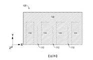
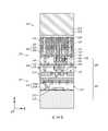
圖1A至圖6B為說明形成微電子裝置(例如,記憶體裝置,諸如三維反及閘快閃記憶體裝置)之微電子裝置結構(例如,記憶體裝置結構)之方法之實施例的簡化部分截面(亦即,圖1A、圖2A、圖3A、圖4A、圖5A及圖6A)及簡化部分平面(亦即,圖1B、圖2B、圖3B、圖4B、圖5B及圖6B)視圖。藉由如下文所提供之描述,一般熟習此項技術者將顯而易見,本文中所描述之方法可用於各種應用中。換言之,每當需要形成微電子裝置時,可使用本發明之方法。1A-6B are simplified portions illustrating an embodiment of a method of forming a microelectronic device structure (eg, a memory device structure) of a microelectronic device (eg, a memory device such as a three-dimensional inverse and gate flash memory device) Cross-sectional (ie, FIGS. 1A, 2A, 3A, 4A, 5A, and 6A) and simplified partial plan (ie, FIGS. 1B, 2B, 3B, 4B, 5B, and 6B) views . From the description provided below, it will be apparent to those of ordinary skill in the art that the methods described herein can be used in a variety of applications. In other words, whenever a microelectronic device needs to be formed, the method of the present invention can be used.
參考圖1A,微電子裝置結構100可形成為包括基底結構101上或上方之導線結構102、導線結構102上或上方之絕緣線結構104,及與導線結構102(及因此絕緣線結構104)水平交錯(例如,在X方向上)之溝槽106。在下文中進一步詳細描述基底結構101、導線結構102、絕緣線結構104及溝槽106。圖1B為在圖1A中所描繪之製程階段處的微電子裝置結構100之簡化平面視圖。Referring to FIG. 1A, a
基底結構101可包含上面可形成其他材料之基底材料或構造。基底結構101可由半導電材料、導電材料及介電材料中之一或多者形成且包括半導電材料、導電材料及介電材料中之一或多者。舉例而言,基底結構101可包含半導電結構(例如,半導體基板);支撐結構上之基底半導電材料;導電結構(例如,金屬電極);介電結構;包括不同材料、結構及區域中之一或多者的結構;另一基底材料;或另一構造。在一些實施例中,基底結構101包含記憶體裝置(例如,三維反及閘快閃記憶體裝置)之堆疊結構,如在下文更詳細地描述。舉例而言,堆疊結構可包括以層級配置之導電結構與絕緣結構之豎直交錯序列。The
導線結構102可呈現在第一水平方向(例如,Y方向)上平行延伸之水平細長形狀。如本文中所使用,術語「平行」意謂實質上平行。導線結構102可各自呈現實質上相同尺寸(例如,X方向上之寬度、Y方向上之長度、Z方向上之高度)、形狀及間距(例如,在X方向上)。在其他實施例中,導線結構102中之一或多者可呈現相較於一或多個其他導線結構102的至少一個不同尺寸(例如,不同長度、不同寬度、不同高度)及不同形狀中之一或多者,且/或至少兩個水平鄰近導線結構102之間的間距(例如,在X方向上)可不同於至少兩個其他水平鄰近導線結構102之間的間距。在一些實施例中,導線結構102用作記憶體裝置之數位線結構(例如,資料線結構、位元線結構),如在下文更詳細地描述。The
導線結構102可由導電材料形成且包括導電材料。藉助於非限制性實例,導線結構102可各自個別地由金屬材料形成且包括該金屬材料,該金屬材料包含以下各者中之一或多者:至少一種金屬、至少一種合金及至少一種含有導電金屬之材料(例如,導電金屬氮化物、導電金屬矽化物、導電金屬碳化物、導電金屬氧化物)。在一些實施例中,導線結構102各自個別地由W形成且包括W。導線結構102中之每一者可個別地為實質上均質的,或導線結構102中之一或多者可個別地為實質上異質的。如本文中所使用,術語「均質」意謂特徵(例如,結構、材料)中包括之元件之相對量貫穿特徵之不同部分(例如,不同水平部分、不同豎直部分)不發生改變。相對而言,如本文中所使用,術語「異質」意謂特徵(例如,材料、結構)中包括之元件之相對量貫穿特徵之不同部分發生改變。若導線結構102為異質的,則導線結構102中包括之一或多個元件之量可貫穿導線結構102之不同部分逐步地改變(例如,突然改變)或可連續地改變(例如,逐漸地改變,諸如線性地、拋物線式)。在一些實施例中,導線結構102中之每一者為實質上均質的。在其他實施例中,導線結構102中之每一者為異質的。舉例而言,每一導線結構102可由至少兩種不同導電材料之堆疊(例如,層壓物)形成且包括至少兩種不同導電材料之堆疊(例如,層壓物)。The
如圖1A所示,絕緣線結構104可豎直地上覆於(例如,直接豎直地上覆於)導線結構102。絕緣線結構104可充當用於導線結構102之絕緣帽結構(例如,介電帽結構)。絕緣線結構104可具有在第一水平方向(例如,Y方向)上平行延伸之水平細長形狀。絕緣線結構104之水平尺寸、水平路徑及水平間距可與導線結構102之水平尺寸、水平路徑及水平間距實質上相同。As shown in FIG. 1A , the
絕緣線結構104可由絕緣材料形成且包括絕緣材料。藉助於非限制性實例,絕緣線結構104可各自個別地由諸如SiNy(例如,Si3N4)之介電氮化物材料形成且包括介電氮化物材料。絕緣線結構104可各自為實質上均質的,或絕緣線結構104中之一或多者可為異質的。若絕緣線結構104為異質的,則絕緣線結構104中包括之一或多個元件之量可貫穿絕緣線結構104之不同部分逐步地改變(例如,突然改變)或可連續地改變(例如,逐漸地改變,諸如線性地、拋物線式)。在一些實施例中,絕緣線結構104中之每一者為實質上均質的。在其他實施例中,絕緣線結構104中之每一者為異質的。舉例而言,每一絕緣線結構104可由至少兩種不同介電材料之堆疊(例如,層壓物)形成且包括至少兩種不同介電材料之堆疊(例如,層壓物)。The
繼續參考圖1A,溝槽106可水平地介入於(例如,在X方向上)水平鄰近導線結構102 (及因此水平鄰近絕緣線結構104)之間且分隔開水平鄰近導線結構102 (及因此水平鄰近絕緣線結構104)。溝槽106可在導線結構102延伸之水平方向(例如,Y方向)上平行延伸。另外,如圖1A中所示,溝槽106可自絕緣線結構104之上部豎直邊界(例如,上表面)豎直地延伸(例如,在Z方向上)至導線結構102之下部豎直邊界(例如,下表面)。導線結構102及絕緣線結構104之側表面可界定溝槽106之水平邊界,導線結構102之下表面可界定溝槽106之下部豎直邊界,且絕緣線結構104之上表面可界定溝槽106之上部豎直邊界。With continued reference to FIG. 1A ,
導線結構102、絕緣線結構104及溝槽106可使用習知製程(例如,習知沈積製程,諸如原位生長、旋塗、毯覆式塗佈、CVD、PECVD、ALD及PVD中之一或多者;習知圖案化製程,諸如習知光微影製程;習知材料移除製程,諸如習知蝕刻製程)及習知處理設備形成,這在本文中未詳細地描述。The
接下來參考圖2A,隔離材料108可形成於微電子裝置結構100之曝露表面上方。隔離材料108可呈現至少部分地由基底結構101、導線結構102及絕緣線結構104之表面(例如,上表面、側表面)之構形界定的實質上平坦的上邊界(例如,上表面)及不平坦的下邊界。隔離材料108可部分地(例如,不完全)填充溝槽106 (圖1A及圖1B)。因此,如圖2A中所示,對應於保持未由隔離材料108填充之溝槽106 (圖1A及圖1B)之部分的氣隙110可在隔離材料108之形成之後水平地介入於(例如,在X方向上)水平鄰近導線結構102及水平鄰近絕緣線結構104之間。氣隙110可充當具有約1之介電常數(k)之絕緣體。氣隙110可限制電容(例如,寄生電容、雜散電容)且增大水平鄰近導線結構102之間的短路裕度,且可減小水平鄰近導線結構102之間的串擾。圖2B為在圖2A中所描繪之製程階段處的微電子裝置結構100之簡化平面視圖。Referring next to FIG. 2A ,
隔離材料108可由至少一種絕緣材料形成且包括至少一種絕緣材料。藉助於非限制性實例,隔離材料108可由以下各者中之一或多者形成且包括以下各者中之一或多者:至少一種介電氧化物材料(例如,SiOx、磷矽酸鹽玻璃、硼矽酸鹽玻璃、硼磷矽玻璃、氟矽酸鹽玻璃、AlOx、HfOx、NbOx及TiOx中之一或多者)、至少一種介電氮化物材料(例如,SiNy)、至少一種介電氮氧化物材料(例如,SiOxNy)、至少一種介電碳氮化物材料(例如,SiOxCzNy)及非晶碳。在一些實施例中,隔離材料108由SiOx(例如,SiO2)形成且包括SiOx(例如,SiO2)。The
如圖2A所示,氣隙110可自豎直地處於或豎直地低於絕緣線結構104之上部豎直邊界之位置豎直地延伸(例如,在Z方向上)至豎直地處於或豎直地高於導線結構102之下部豎直邊界之其他位置。在一些實施例中,氣隙110自豎直地低於絕緣線結構104之上表面且豎直地高於導線結構102之上表面的位置豎直地延伸至豎直地高於導線結構102之下表面之其他位置。氣隙110可各自個別地實質上由隔離材料108環繞(例如,埋入該隔離材料內、嵌入該隔離材料內)。另外,氣隙110可圍繞溝槽106 (圖1A)之水平中心線(例如,在X方向上)定位,且可自溝槽106 (圖1A)之水平中心線向外水平地延伸(例如,在X方向上)。As shown in FIG. 2A , the
隔離材料108及氣隙110可使用習知製程(例如,習知沈積製程、習知材料移除製程)及習知處理設備形成,這在本文中未詳細地描述。舉例而言,隔離材料108 (及因此氣隙110)可使用一或多種習知非保形沈積製程(例如,至少一種習知非保形PVD製程)形成於微電子裝置結構100之曝露表面之部分上或上方。此後,隔離材料108可經歷至少一個習知平坦化製程(例如,至少一個習知CMP製程)以有助於或增強隔離材料108之上邊界(例如,上表面)之平坦度。以上文所描述之方式形成氣隙110可實現微電子裝置結構100之水平鄰近導電性特徵(例如,導線結構102)之間的非所要電容耦合之減小,同時避開可在氣隙110經由其他製程,諸如藉由蝕刻形成於導線結構102之間的絕緣材料而形成之情況下以其他方式發生的對水平鄰近導電性特徵之非所要損害。因此,以上文所描述之方式形成氣隙110可保持水平鄰近導電性特徵及氣隙110兩者之完整性。
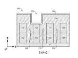
接下來參考圖3A,豎直地上覆於絕緣線結構104的隔離材料108之部分可經移除(例如,經蝕刻)以曝露(例如,露出)絕緣線結構104之部分。如圖3A中所示,材料移除製程可形成自隔離材料108之上表面豎直地延伸(例如,在Z方向上)至絕緣線結構104之開口112。在一些實施例中,材料移除製程移除隔離材料108之預定部分而不移除絕緣線結構104之部分。在其他實施例中,材料移除製程移除隔離材料108之預定部分且亦部分地移除豎直地下伏於且與隔離材料108之預定部分水平地重疊(例如,至少部分地水平對準)的絕緣線結構104之部分。圖3B為在圖3A中所描繪之製程階段處的微電子裝置結構100之簡化平面視圖。Referring next to FIG. 3A , portions of
如圖3B所示,個別開口112可在X方向上與個別絕緣線結構104 (及因此個別導線結構102 (圖3A))至少部分地(例如,實質上)水平對準。舉例而言,在X方向上的開口112之水平中心線可與在X方向上的絕緣線結構104之水平中心線實質上對準。每一開口112可水平地定位於在X方向上彼此水平鄰近之兩個氣隙110之間。另外,個別開口112可沿著個別絕緣線結構104 (及因此個別導線結構102 (圖3A))在Y方向上定位於所要位置處。在一些實施例中,開口112中之至少一些設置於在Y方向上彼此不同之位置處。舉例而言,相較於沿著絕緣線結構104中之第二者在Y方向上之長度的開口112中之第二者之位置,開口112中之第一者可沿著絕緣線結構104中之第一者在Y方向上之長度設置於不同位置處。換言之,開口112中之至少一些(例如,全部)可在Y方向上彼此水平地偏移。在其他實施例中,開口112中之兩者或更多者在Y方向上彼此水平對準。As shown in FIG. 3B , the
開口112可各自個別地形成為呈現幾何組態(例如,尺寸、形狀),其有助於隨後形成於開口中之其他特徵(例如,其他結構、其他材料)之所要幾何組態。如圖3B所示,在一些實施例中,個別開口112形成為在X方向上相較於豎直地在該等開口下方之個別絕緣線結構104 (及因此個別導線結構102 (圖3A))相對較寬。舉例而言,每一開口112可在X方向上水平地延伸超出與其相關聯(例如,由此曝露)之絕緣線結構104在X方向上之水平邊界。在一些實施例中,每一開口112在X方向上之寬度為與其相關聯的絕緣線結構104在X方向上之寬度的至多兩倍(2X),諸如在自約絕緣線結構104在X方向上之寬度的一又四分之一倍(1.25X)至約絕緣線結構104在X方向上之寬度的兩倍(2X)的範圍內。開口112可在絕緣線結構104與水平地鄰近絕緣線結構104之氣隙110之水平邊界之間在X方向上水平地終止,使得開口112並不與氣隙110水平地重疊;或開口112可在水平地鄰近絕緣線結構104之氣隙110之水平邊界內在X方向上水平地終止,使得開口112部分地與氣隙110水平地重疊。在其他實施例中,開口112中之一或多者(例如,每一者)個別地形成為呈現小於或等於與其相關聯的絕緣線結構104在X方向上之寬度的X方向上之寬度。另外,如圖3B中所示,相較於豎直地在該等開口下方之個別絕緣線結構104 (及因此個別導線結構102 (圖3A)),個別開口112可形成為具有小於Y方向上之長度的Y方向上之長度。在一些實施例中,每一開口112形成為具有實質上正方形的水平截面形狀。在其他實施例中,開口112中之一或多者(例如,每一者)形成為具有不同(例如,非正方形)水平截面形狀,諸如圓形水平截面形狀、不同的四邊形水平截面形狀、卵形水平截面形狀、橢圓形水平截面形狀及三角形水平截面形狀中之一或多者。開口112中之每一者可形成為呈現與開口112彼此實質上相同的幾何組態,或開口112中之一或多者可形成為呈現與開口112中之一或多個其他者不同的幾何組態。The
開口112可使用一或多個習知材料移除製程(例如,習知各向異性蝕刻製程)形成,這在本文中未詳細地描述。舉例而言,隔離材料108之預定部分可藉由各向異性乾式蝕刻(例如,反應性離子蝕刻(RIE)、深度RIE、電漿蝕刻、反應性離子束蝕刻、化學輔助離子束蝕刻)及各向異性濕式蝕刻(例如,氫氟酸(HF)蝕刻、緩衝HF蝕刻、緩衝氧化物蝕刻)中之一或多者來移除。
接下來參考圖4A,視需要,間隔件材料114可形成於開口112內部及外部的隔離材料108及絕緣線結構104之表面上或上方。舉例而言,如圖4A中所示,間隔件材料114可保形地形成於界定開口112之水平邊界的隔離材料108之表面(例如,側表面)上、界定開口112之下部豎直邊界的絕緣線結構104及隔離材料108之表面上,及開口112外部的隔離材料108之表面(例如,上表面)上。如圖4A中所示,間隔件材料114 (若存在)可部分地(例如,不完全)填充開口112。圖4B為在圖4A中所描繪之製程階段處的微電子裝置結構100之簡化平面視圖。為了清楚且易於理解圖式及相關聯描述起見,開口112之水平邊界外部的間隔件材料114之部分在圖4B中省略。然而,如圖4A中所示且如上文所描述,間隔件材料114 (若存在)可形成為水平地延伸超出開口112之水平邊界。Referring next to FIG. 4A ,
間隔件材料114 (若存在)可由具有不同於絕緣線結構104之蝕刻選擇性之至少一種絕緣材料形成且包括至少一種絕緣材料。間隔件材料114可在曝露於第一蝕刻劑之共同(例如,集合、相互)曝露期間相對於絕緣線結構104選擇性地蝕刻,且絕緣線結構104可在曝露於第二不同蝕刻劑之共同曝露期間相對於間隔件材料114選擇性地蝕刻。如本文中所使用,若材料呈現比另一材料之蝕刻速率高至少約三倍(3x),諸如高約五倍(5x)、高約十倍(10x)、高約二十倍(20x)或高約四十倍(40x)的蝕刻速率,則材料可相對於另一材料「選擇性地蝕刻」。藉助於非限制性實例,間隔件材料114可由以下各者中之一或多者形成且包括以下各者中之一或多者:至少一種介電氧化物材料(例如,SiOx、磷矽酸鹽玻璃、硼矽酸鹽玻璃、硼磷矽玻璃、氟矽酸鹽玻璃、AlOx、HfOx、NbOx、TiOx、ZrOx、TaOx及MgOx中之一或多者)、至少一種介電氮化物材料(例如,SiNy)、至少一種介電氮氧化物材料(例如,SiOxNy)及至少一種介電碳氮化物材料(例如,SiOxCzNy)。在一些實施例中,諸如絕緣線結構104由至少一種介電氮化物材料(例如,SiNy,諸如Si3N4)形成且包括至少一種介電氮化物材料的一些實施例,間隔件材料114由至少一種介電氧化物材料(例如,SiOx,諸如SiO2)形成且包括至少一種介電氧化物材料。
間隔件材料114 (若存在)可形成為任何所要厚度,至少部分地取決於個別絕緣線結構104 (及因此導線結構102)與水平地鄰近絕緣線結構104之個別氣隙110之間的水平距離(例如,在X方向上)。間隔件材料114可用以形成在微電子裝置結構100之後續處理期間至少部分地保護(例如,保持、維持)氣隙110之間隔件結構,如在下文更詳細地描述。藉助於非限制性實例,間隔件材料114 (若存在)可形成為具有在自約10奈米(nm)至約100 nm,諸如自約20 nm至約75 nm或自約30 nm至約50 nm範圍內之厚度。在一些實施例中,間隔件材料114形成為呈現在自約30 nm至約50 nm範圍內之厚度。The spacer material 114 (if present) can be formed to any desired thickness, depending at least in part on the horizontal distance between the individual insulated wire structures 104 (and thus the wire structures 102 ) and the
間隔件材料114 (若存在)可使用習知製程及習知處理設備形成,這在本文中未詳細地描述。藉助於非限制性實例,間隔件材料114可經由保形CVD製程及ALD製程中之一或多者保形地形成於微電子裝置結構100之曝露表面上。The
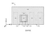
接下來參考圖5A,間隔件材料114 (圖4A及圖4B)(若存在)及開口112 (圖4A及圖4B)之水平邊界內的絕緣線結構104之部分可經歷至少一個材料移除製程以由間隔件材料114 (圖4A及圖4B)形成間隔件結構116且選擇性地移除絕緣線結構104之部分。如圖5A中所示,材料移除製程可形成豎直地延伸至且曝露(例如,露出)導線結構102之部分的延伸開口118。圖5B為在圖5A中所描繪之製程階段處的微電子裝置結構100之簡化平面視圖。Referring next to FIG. 5A, the portion of the
如圖5A所示,材料移除製程可實質上(例如,完全)移除開口112 (圖4A及圖4B)之水平邊界外部的隔離材料108之上表面上或上方的間隔件材料114 (若存在)之部分,且可部分地移除開口112之下部豎直邊界處的間隔件材料114之部分。間隔件結構116 (若存在)在開口112之水平邊界處可包含隔離材料108之側表面上的間隔件材料114之剩餘(例如,未經移除)部分。在未形成間隔件材料114之其他實施例中,自微電子裝置結構100省略(例如,不存在)間隔件結構116。As shown in FIG. 5A, the material removal process can substantially (eg, completely) remove
仍參考圖5A,材料移除製程可移除開口112 (圖4A及圖4B)之水平邊界(例如,在X方向及Y方向上)內的絕緣線結構104之部分以形成延伸開口118。延伸開口118可包括包含開口112 (圖4A及圖4B)之剩餘(例如,未填充)部分之上部部分118A,及豎直地下伏於且與上部部分118A相連之下部部分118B。如圖5A所示,延伸開口118之下部部分118B可在X方向上水平地窄於延伸開口118之上部部分118A。在一些實施例中,間隔件結構116之內部側表面界定延伸開口118之上部部分118A之水平邊界,且豎直地下伏於間隔件結構116的隔離材料108之內部側表面界定延伸開口118之下部部分118B之水平邊界。延伸開口118可自隔離材料108之上部豎直邊界(例如,上表面)豎直地延伸(例如,在Z方向上)至導線結構102之上部豎直邊界(例如,上表面)。Still referring to FIG. 5A , a material removal process may remove portions of the
間隔件結構116 (若存在)及延伸開口118可使用習知製程(例如,習知各向異性蝕刻製程)及習知處理設備形成,這在本文中未詳細地描述。在一些實施例中,第一各向異性乾式蝕刻製程用於移除間隔件材料114 (圖4A及圖4B)之部分且形成間隔件結構116,且接著第二各向異性乾式蝕刻製程用於選擇性地移除絕緣線結構104之新近曝露(例如,露出)部分且形成延伸開口118。第一各向異性乾式蝕刻製程可採用第一乾式蝕刻劑,其相較於絕緣線結構104具有朝向間隔件材料114 (圖4A及圖4B)之較高蝕刻選擇性;且第二各向異性乾式蝕刻製程可採用第二乾式蝕刻劑,其相較於間隔件材料114 (圖4A及圖4B)具有朝向絕緣線結構104之較高蝕刻選擇性。Spacer structures 116 (if present) and
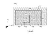
接下來參考圖6A,導電接觸結構120可形成於延伸開口118 (圖5A及圖5B)內,且導電襯墊結構124可形成於導電接觸結構120上或上方。導電接觸結構120可實質上受限於延伸開口118 (圖5A及圖5B)之邊界(例如,水平邊界、豎直邊界)內,且導電襯墊結構124可至少部分地定位於延伸開口118 (圖5A及圖5B)之邊界外部。另外,其他隔離材料122可形成於隔離材料108上或上方,且可水平地鄰近導電襯墊結構124。圖6B為在圖6A中所描繪之製程階段處的微電子裝置結構100之簡化平面視圖。為了清楚且易於理解圖式及相關聯描述起見,其他隔離材料122在圖6B中省略。Referring next to FIG. 6A ,
如圖6A所示,導電接觸結構120可實質上填充延伸開口118 (圖5A及圖5B),且可呈現與隔離材料108及間隔件結構116 (若存在)之上表面實質上共面的實質上平坦的上表面。導電接觸結構120可自隔離材料108及間隔件結構116 (若存在)之上邊界(例如,上表面)豎直地延伸(例如,在Z方向上)至導線結構102之上邊界(例如,上表面)。在一些實施例中,導電接觸結構120之尺寸、形狀及間距分別與延伸開口118 (圖5A及圖5B)之尺寸、形狀及間距實質上相同。導電接觸結構120可耦接至導線結構102。在一些實施例中,導電接觸結構120用作用於記憶體裝置之數位線接觸結構(例如,資料線接觸結構、位元線接觸結構),如在下文更詳細地描述。As shown in FIG. 6A, the
導電接觸結構120可各自個別地由導電材料形成且包括導電材料。藉助於非限制性實例,導電接觸結構120可由以下各者中之一或多者形成且包括以下各者中之一或多者:至少一種金屬、至少一種合金及至少一種含有導電金屬之材料(例如,導電金屬氮化物、導電金屬矽化物、導電金屬碳化物、導電金屬氧化物)。在一些實施例中,導電接觸結構120由Cu形成且包括Cu。在其他實施例中,導電接觸結構120由W形成且包括W。The
導電接觸結構120可使用習知製程及習知處理設備形成,這在本文中未詳細地描述。藉助於非限制性實例,導電材料可形成於(例如,非保形地沈積於)延伸開口118 (圖5A及圖5B)內部及外部,且接著延伸開口118 (圖5A及圖5B)之邊界(例如,水平邊界、豎直邊界)外部的導電材料之部分可經移除(例如,經由至少一個材料移除製程,諸如至少一個CMP製程)以形成導電接觸結構120。The
繼續參考圖6A,其他隔離材料122可形成於隔離材料108之上表面上或上方。其他隔離材料122可由至少一種絕緣材料形成且包括至少一種絕緣材料。藉助於非限制性實例,其他隔離材料122可由以下各者中之一或多者形成且包括以下各者中之一或多者:至少一種介電氧化物材料(例如,SiOx、磷矽酸鹽玻璃、硼矽酸鹽玻璃、硼磷矽玻璃、氟矽酸鹽玻璃、AlOx、HfOx、NbOx及TiOx中之一或多者)、至少一種介電氮化物材料(例如,SiNy)、至少一種介電氮氧化物材料(例如,SiOxNy)、至少一種介電碳氮化物材料(例如,SiOxCzNy)及非晶碳。其他隔離材料122之材料組成可與隔離材料108之材料組成實質上相同,或其他隔離材料122之材料組成可不同於隔離材料108之材料組成。在一些實施例中,其他隔離材料122由SiOx(例如,SiO2)形成且包括SiOx(例如,SiO2)。With continued reference to FIG. 6A ,
導電襯墊結構124可形成於導電接觸結構120、間隔件結構116 (若存在)及隔離材料108之表面上或上方。導電襯墊結構124可形成於形成於其他隔離材料122內之孔隙內且可實質上填充孔隙。如圖6A及圖6B中所示,導電襯墊結構124可形成為在多個絕緣線結構104 (及因此多個導線結構102)及氣隙110上方水平地延伸。個別導電襯墊結構124可耦接至個別導電接觸結構120。導電襯墊結構124可用作接合襯墊以將導電接觸結構120耦接至其他導電襯墊結構及其他導電接觸結構,如在下文更詳細地描述。
導電襯墊結構124可各自個別地由導電材料形成且包括導電材料。藉助於非限制性實例,導電襯墊結構124可由以下各者中之一或多者形成且包括以下各者中之一或多者:至少一種金屬、至少一種合金及至少一種含有導電金屬之材料(例如,導電金屬氮化物、導電金屬矽化物、導電金屬碳化物、導電金屬氧化物)。導電襯墊結構124之材料組成可與導電接觸結構120之材料組成實質上相同,或導電襯墊結構124之材料組成可不同於導電接觸結構120之材料組成。在一些實施例中,導電襯墊結構124由Cu形成且包括Cu。The
其他隔離材料122及導電襯墊結構124可使用習知製程及習知處理設備形成,這在本文中未詳細地描述。作為非限制性實例,其他隔離材料122可(例如,經由至少一個材料沈積製程,諸如ALD製程、CVD製程、PECVD製程、PVD製程及旋塗製程中之一或多者)形成於導電接觸結構120、間隔件結構116 (若存在)及隔離材料108之曝露表面上或上方;孔隙可形成(例如,蝕刻)於其他隔離材料122內;且接著導電襯墊結構124可經由金屬鑲嵌製程形成於孔隙內。金屬鑲嵌製程可包括藉由導電材料填充孔隙(例如,經由至少一個其他材料沈積製程,諸如ALD製程、CVD製程、PECVD製程、PVD製程及旋塗製程中之一或多者),且接著使用至少一個平坦化製程(例如,至少一個CMP製程)移除孔隙之邊界(例如,水平邊界、豎直邊界)外部的導電材料之部分。作為另一非限制性實例,導電材料可(例如,經由至少一個材料沈積製程,諸如ALD製程、CVD製程、PECVD製程、PVD製程及旋塗製程中之一或多者)形成於導電接觸結構120、間隔件結構116 (若存在)及隔離材料108之曝露表面上或上方;導電材料之部分可經移除(例如,經蝕刻)以經由減色製程形成導電襯墊結構124;且接著可圍繞導電襯墊結構124形成(例如,使用至少一個材料沈積製程及至少一個平坦化製程)其他隔離材料122。
上文參考圖1A至圖6B所描述之本發明之方法可有助於導電襯墊結構124與導線結構102之自對準,且可相較於在類似導線結構上方形成導電接合襯墊結構之習知方法避免或放寬疊對約束。相較於形成所要微電子裝置結構之習知方法,本發明之方法可減小形成所要微電子裝置結構所需的處理動作(例如,對準及遮蔽動作)、材料及結構之數目。The methods of the present invention described above with reference to FIGS. 1A-6B may facilitate self-alignment of
因此,根據本發明之實施例,形成微電子裝置之方法包含形成包含導電材料及上覆於該導電材料之絕緣材料之線結構,該等線結構藉由溝槽彼此分隔開。隔離材料形成於該等溝槽內部及外部之該等線結構之表面上,該隔離材料僅部分地填充該等溝槽以形成插入於該等線結構之間的氣隙。開口形成為延伸穿過該隔離材料且曝露該等線結構之該絕緣材料之部分。移除該等線結構之該絕緣材料之曝露部分以形成延伸至該等線結構之該導電材料之延伸開口。導電接觸結構形成於該等延伸開口內。導電襯墊結構形成於該等導電接觸結構上。亦描述了其他方法、微電子裝置、記憶體裝置及電子系統。Thus, in accordance with an embodiment of the present invention, a method of forming a microelectronic device includes forming a line structure comprising a conductive material and an insulating material overlying the conductive material, the line structures being separated from each other by trenches. An isolation material is formed on the surfaces of the line structures inside and outside the trenches, the isolation material only partially fills the trenches to form air gaps interposed between the line structures. Openings are formed extending through the isolation material and exposing portions of the insulating material of the line structures. The exposed portions of the insulating material of the line structures are removed to form extended openings of the conductive material extending to the line structures. Conductive contact structures are formed within the extended openings. Conductive pad structures are formed on the conductive contact structures. Other methods, microelectronic devices, memory devices, and electronic systems are also described.
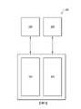
根據本發明之實施例的微電子裝置結構(例如,在上文參考圖6A及圖6B所描述之製程階段之後的微電子裝置結構100)可用於本發明之微電子裝置(例如,記憶體裝置,諸如三維反及閘快閃記憶體裝置)中。藉助於非限制性實例,圖7為根據本發明之實施例的微電子裝置200 (例如,記憶體裝置,諸如三維反及閘快閃記憶體裝置)之簡化部分截面視圖。如圖7所示且在下文中進一步詳細描述,微電子裝置200可包括由完成先前參考圖6A及圖6B所描述之製程階段產生的微電子裝置結構100。藉由下文所提供之描述,一般熟習此項技術者將顯而易見,本文中所描述之微電子裝置可包括於各種相對較大的裝置及各種電子系統中。Microelectronic device structures according to embodiments of the present invention (eg,
如圖7所示,微電子裝置200可包括控制邏輯區域202、記憶體陣列區域204、第一互連區域206及第二互連區域208。如圖7中所示,第一互連區域206可豎直地上覆於(例如,在Z方向上)控制邏輯區域202並與控制邏輯區域電連通,且記憶體陣列區域204可豎直地上覆於第一互連區域206並與第一互連區域電連通。第一互連區域206可豎直地插入於控制邏輯區域202與記憶體陣列區域204之間且與控制邏輯區域及記憶體陣列區域電連通。另外,第二互連區域208可豎直地上覆於記憶體陣列區域204且與記憶體陣列區域電連通。記憶體陣列區域204可豎直地插入於第一互連區域206與第二互連區域208之間且與第一互連區域及第二互連區域電連通。先前參考圖6A及圖6B所描述之微電子裝置結構100可形成微電子裝置200之記憶體陣列區域204及第一互連區域206之部分。As shown in FIG. 7 , the
微電子裝置200之控制邏輯區域202可包括半導電基底結構210、閘極結構212、第一佈線結構214及第一接觸結構216。半導電基底結構210、閘極結構212、第一佈線結構214及第一接觸結構216之部分形成控制邏輯區域202之各種控制邏輯裝置215,如在下文更詳細地描述。The
控制邏輯區域202之半導電基底結構210 (例如,半導電晶圓)包含基底材料或構造,其上形成有微電子裝置200之其他特徵(例如,材料、結構、裝置)。半導電基底結構210可包含半導電結構(例如,半導電晶圓)或處於支撐結構上之基底半導電材料。舉例而言,半導電基底結構210可包含習知矽基板(例如,習知矽晶圓),或包含半導電材料之另一塊體基板。在一些實施例中,半導電基底結構210包含矽晶圓。另外,半導電基底結構210可包括其中及/或其上形成之一或多個層、結構及/或區域。舉例而言,半導電基底結構210可包括導電摻雜區域及未摻雜區域。導電摻雜區域可例如用作控制邏輯區域202之控制邏輯裝置215之電晶體的源極區域及汲極區域;且未摻雜區域可例如用作控制邏輯裝置215之電晶體的通道區域。The semiconducting base structure 210 (eg, a semiconducting wafer) of the
如圖7所示,微電子裝置200之控制邏輯區域202之閘極結構212可豎直地上覆於(例如,在Z方向上)半導電基底結構210之部分。閘極結構212可個別地在微電子裝置200之控制邏輯區域202內的控制邏輯裝置215之電晶體之間水平地延伸且由該等電晶體採用。閘極結構212可由導電材料形成且包括導電材料。閘極介電材料(例如,介電氧化物)可豎直地介入於(例如,在Z方向上)閘極結構212與電晶體之通道區域(例如,半導電基底結構210內)之間。As shown in FIG. 7 , the
第一佈線結構214可豎直地上覆於(例如,在Z方向上)半導電基底結構210,且可藉助於第一接觸結構216電連接至半導電基底結構210。第一佈線結構214可充當微電子裝置200之局部佈線結構。第一接觸結構216之第一群組216A可在半導電基底結構210之區域(例如,導電摻雜區域,諸如源極區域及汲極區域)與第一佈線結構214中之一或多者之間豎直地延伸且將該等區域耦接至該一或多者。另外,第一接觸結構216之第二群組216B可在第一佈線結構214中之一些之間豎直地延伸且將其彼此耦接。The
第一佈線結構214可各自個別地由導電材料形成且包括導電材料。藉助於非限制性實例,第一佈線結構214可由以下各者中之一或多者形成且包括以下各者中之一或多者:至少一種金屬、至少一種合金及至少一種含有導電金屬之材料(例如,導電金屬氮化物、導電金屬矽化物、導電金屬碳化物、導電金屬氧化物)。在一些實施例中,第一佈線結構214由Cu形成且包括Cu。在其他實施例中,第一佈線結構214由W形成且包括W。The
第一接觸結構216 (包括其第一群組216A及第二群組216B)可各自個別地由導電材料形成且包括導電材料。藉助於非限制性實例,第一佈線結構214可由以下各者中之一或多者形成且包括以下各者中之一或多者:至少一種金屬、至少一種合金及至少一種含有導電金屬之材料(例如,導電金屬氮化物、導電金屬矽化物、導電金屬碳化物、導電金屬氧化物)。在一些實施例中,第一接觸結構216由Cu形成且包括Cu。在其他實施例中,第一接觸結構216由W形成且包括W。在其他實施例中,第一接觸結構216之第一群組216A中的第一接觸結構216由第一導電材料(例如,W)形成且包括第一導電材料;且第一接觸結構216之第二群組216B中的第一接觸結構216由第二不同導電材料(例如,Cu)形成且包括第二不同導電材料。The first contact structures 216 (including the
如先前所提及,半導電基底結構210之部分(例如,充當源極區域及汲極區域之導電摻雜區域、充當通道區域之未摻雜區域)、閘極結構212、第一佈線結構214及第一接觸結構216形成控制邏輯區域202之各種控制邏輯裝置215。在一些實施例中,控制邏輯裝置215包含互補金屬氧化物半導體(CMOS)電路系統。控制邏輯裝置215可經組態以控制微電子裝置200之其他組件(例如,記憶體陣列區域204內之記憶體單元)的各種操作。作為非限制性實例,控制邏輯裝置215可包括電荷泵(例如,VCCP電荷泵、VNEGWL電荷泵、DVC2電荷泵)、延遲鎖定迴路(DLL)電路系統(例如,環式振盪器)、Vdd調節器、串驅動器、頁面緩衝器及各種晶片/層面控制電路系統中之一或多者(例如,每一者)。作為另一非限制性實例,控制邏輯裝置215可包括經組態以控制微電子裝置200之記憶體陣列區域204內的陣列(例如,記憶體元件陣列、存取裝置陣列)之行操作的裝置,諸如解碼器(例如,本端層面解碼器、行解碼器)、感測放大器(例如,均衡(EQ)放大器、隔離(ISO)放大器、NMOS感測放大器(NSA)、PMOS感測放大器(PSA))、修復電路系統(例如,行修復電路系統)、I/O裝置(例如,本端I/O裝置)、記憶體測試裝置、陣列多工器(MUX)及誤差檢查與校正(ECC)裝置中之一或多者(例如,每一者)。作為另一非限制性實例,控制邏輯裝置215可包括經組態以控制微電子裝置200之記憶體陣列區域204內的陣列(例如,記憶體元件陣列、存取裝置陣列)之列操作的裝置,諸如解碼器(例如,本端層面解碼器、列解碼器)、驅動器(例如,WL驅動器)、修復電路系統(例如,列修復電路系統)、記憶體測試裝置、MUX、ECC裝置及自再新/損耗平衡裝置中之一或多者(例如,每一者)。As previously mentioned, portions of semiconducting base structure 210 (eg, conductive doped regions serving as source and drain regions, undoped regions serving as channel regions),
仍參考圖7,微電子裝置200之記憶體陣列區域204可包括堆疊結構218;微電子裝置結構100之部分,包括導線結構102、絕緣線結構104、隔離材料108及氣隙110;以及源極層級237,包括一或多個源極結構238及一或多個接觸襯墊240。堆疊結構218可對應於微電子裝置結構100之先前參考圖1A及圖1B所描述之基底結構101。另外,導線結構102可充當微電子裝置200之數位線結構(例如,資料線結構、位元線結構),且絕緣線結構104可充當微電子裝置200之數位線帽結構(例如,資料線帽結構、位元線帽結構)。堆疊結構218可豎直地插入於導線結構102與源極層級237之間。導線結構102可豎直地下伏於(例如,在Z方向上)堆疊結構218,且可電連接至堆疊結構218內之特徵(例如,柱結構、填充通孔)。源極層級237可豎直地上覆於(例如,在Z方向上)堆疊結構218。源極層級237之源極結構238及接觸襯墊240可耦接(例如,電連接)至堆疊結構218內之特徵(例如,柱結構、填充通孔)及微電子裝置200之第二互連區域208內之其他特徵(例如,互連結構)。如圖7中所示,微電子裝置結構100之導電接觸結構120之部分亦可位於微電子裝置200之記憶體陣列區域204內。導電接觸結構120之其他部分可位於微電子裝置200之第一互連區域206內。Still referring to FIG. 7, the
記憶體陣列區域204之堆疊結構218包括以層級224配置之導電結構220與絕緣結構222的豎直交錯(例如,在Z方向上)序列。堆疊結構218之層級224中之每一者可包括豎直鄰近絕緣結構222中之至少一者的導電結構220中之至少一者。在一些實施例中,導電結構220由鎢(W)形成且包括鎢,且絕緣結構222由二氧化矽(SiO2)形成且包括二氧化矽。堆疊結構218之層級224的導電結構220及絕緣結構222可各自個別地為實質上平坦的,且可各自個別地呈現所要厚度。The
如圖7所示,一或多個深接觸結構226可豎直地延伸穿過堆疊結構218。深接觸結構226可經組態及定位以將微電子裝置200之豎直地上覆於堆疊結構218的一或多個組件與微電子裝置200之豎直地下伏於堆疊結構218的一或多個其他組件電連接。深接觸結構226可由導電材料形成且包括導電材料。在一些實施例中,深接觸結構由W形成且包括W。As shown in FIG. 7 , one or more
如圖7所示,記憶體陣列區域204進一步包括豎直地延伸穿過堆疊結構218之單元柱結構228。單元柱結構228可各自個別地包括至少部分地由一或多個電荷儲存結構(例如,電荷捕集結構,諸如包含氧化物-氮化物-氧化物(「ONO」)材料之電荷捕集結構;浮動閘極結構)環繞的半導電柱(例如,多晶矽柱、矽鍺柱)。單元柱結構228與堆疊結構218之層級224之導電結構220的交叉點可界定微電子裝置200之記憶體陣列區域204內的彼此串聯耦接之記憶體單元230的豎直延伸串。在一些實施例中,在堆疊結構218之層級224內形成於導電結構220與單元柱結構228之交叉點處的記憶體單元230包含所謂的「MONOS」(金屬-氧化物-氮化物-氧化物-半導體)記憶體單元。在其他實施例中,記憶體單元230包含所謂的「TANOS」(氮化鉭-氧化鋁-氮化物-氧化物-半導體)記憶體單元,或所謂的「BETANOS」(經頻帶/阻障工程設計之TANOS)記憶體單元,其中每一者為MONOS記憶體單元之子集。在其他實施例中,記憶體單元包含所謂的「浮動閘極」記憶體單元,其包括浮動閘極(例如,金屬性浮動閘極)作為電荷儲存結構。浮動閘極可水平地介入於單元柱結構228與堆疊結構218之不同層級224之導電結構220的中心結構之間。As shown in FIG. 7 , the
如圖7所示,導線結構102可豎直地插入於堆疊結構218與下伏於堆疊結構218之第一互連區域206之間。個別導線結構102可耦接至記憶體單元230之個別豎直延伸串。在一些實施例中,導線結構102與單元柱結構228直接實體接觸。在其他實施例中,接觸結構可豎直地介入於導線結構102與單元柱結構228之間,且可將導線結構102耦接至記憶體單元230之豎直延伸串。As shown in FIG. 7 , the
繼續參考圖7,源極層級237可豎直地插入於堆疊結構218與上覆於堆疊結構218之第二互連區域208之間。在源極層級237內,源極結構238及接觸襯墊240可水平地彼此鄰近(例如,在X方向上,在Y方向上)。源極結構238可與接觸襯墊240電隔離,且可定位在與接觸襯墊240實質上相同的豎直位置處(例如,在Z方向上)。至少一種絕緣材料可水平地插入於源極結構238與接觸襯墊240之間,如在下文更詳細地描述。With continued reference to FIG. 7 , the
源極層級237之源極結構238可耦接至記憶體單元230之豎直延伸串。在一些實施例中,源極結構238與單元柱結構228直接實體接觸。在其他實施例中,接觸結構可豎直地介入於源極結構238與單元柱結構228之間,且可將源極結構238耦接至記憶體單元230之豎直延伸串。另外,源極結構238可耦接至第二互連區域208內的其他結構(例如,接觸結構、佈線結構、襯墊結構),如在下文更詳細地描述。
源極層級237之接觸襯墊240可耦接至堆疊結構218內之其他導電特徵(例如,導電接觸結構、導電柱、導電填充通孔)。舉例而言,如圖7中所示,接觸襯墊240可耦接至豎直地延伸穿過堆疊結構218之深接觸結構226。在一些實施例中,接觸襯墊240與深接觸結構226直接實體接觸。在其他實施例中,其他接觸結構可豎直地介入於接觸襯墊240與深接觸結構226之間,且可將接觸襯墊240耦接至深接觸結構226。另外,接觸襯墊240可耦接至第二互連區域208內的其他結構(例如,互連結構、佈線結構、襯墊結構),如在下文更詳細地描述。Contact
源極結構238及接觸襯墊240可各自由導電材料形成且包括導電材料。源極結構238之材料組成可與接觸襯墊240之材料組成實質上相同。在一些實施例中,源極結構238及接觸襯墊240由導電摻雜半導電材料形成且包括導電摻雜半導電材料,諸如以下各者中之一或多者的導電摻雜形式:矽材料,諸如單晶矽或多晶矽;矽鍺材料;鍺材料;砷化鎵材料;氮化鎵材料;以及磷化銦材料。作為非限制性實例,源極結構238及接觸襯墊240可由摻雜有至少一種摻雜劑(例如,至少一種n型摻雜劑、至少一種p型摻雜劑及至少另一摻雜劑中之一或多者)之磊晶矽(例如,經由磊晶生長形成之單晶矽)形成且包括磊晶矽。作為另一非限制性實例,源極結構238及接觸襯墊240可由摻雜有至少一種摻雜劑(例如,至少一種n型摻雜劑、至少一種p型摻雜劑及至少另一摻雜劑中之一或多者)之多晶矽形成且包括多晶矽。The
如圖7所示,視需要,跨接結構241可位於源極結構238及接觸襯墊240上或上方。跨接結構241可豎直地插入於源極結構238及接觸襯墊240與第二互連區域208內之其他特徵(例如,其他結構、其他材料)之間。若存在,跨接結構241可由導電材料形成且包括導電材料。可選擇跨接結構241之材料組成以降低第二互連區域208內之導電結構與源極層級237之源極結構238及接觸襯墊240中之每一者之間的接觸電阻(相對於跨接結構241不存在處之組態)。藉助於非限制性實例,跨接結構241 (若存在)可由金屬材料形成且包括該金屬材料,該金屬材料包含以下各者中之一或多者:至少一種金屬、至少一種合金及至少一種含有導電金屬之材料(例如,導電金屬氮化物、導電金屬矽化物、導電金屬碳化物、導電金屬氧化物)。在一些實施例中,跨接結構241由矽化鎢(WSix)形成且包括矽化鎢。在其他實施例中,跨接結構241由W及氮化鎢(WNx)中之一或多者(例如,堆疊)形成且包括W及氮化鎢中之一或多者(例如,堆疊)。As shown in FIG. 7 ,
繼續參考圖7,微電子裝置200之第一互連區域206可豎直地插入於微電子裝置200之控制邏輯區域202與記憶體陣列區域204之間。第一互連區域206可耦接控制邏輯區域202之特徵與記憶體陣列區域204之特徵。如圖7中所示,第一互連區域206可包括耦接至控制邏輯區域202之第一佈線結構214之第二接觸結構242;耦接至記憶體陣列區域204之導線結構102的微電子裝置結構100之導電接觸結構120之部分;以及在第二接觸結構242與導電接觸結構120之間延伸且耦接該等第二接觸結構與該等導電接觸結構之經連接接合襯墊246。經連接接合襯墊246可包括第二接觸結構242上(例如,豎直地上覆於該第二接觸結構且與該第二接觸結構直接相鄰)之第一接合襯墊248,及微電子裝置結構100之導電襯墊結構124 (充當第二接合襯墊)。第一接合襯墊248及導電襯墊結構124可實體上彼此連接以形成經連接接合襯墊246。Continuing to refer to FIG. 7 , the
第一互連區域206之第二接觸結構242可自第一接合襯墊248且在其與控制邏輯區域202之第一佈線結構214中的一些之間豎直地延伸。在一些實施例中,第二接觸結構242包含豎直地延伸穿過插入於第一接合襯墊248與第一佈線結構214之間的介電材料的導電填充通孔。第二接觸結構242可由導電材料形成且包括導電材料。藉助於非限制性實例,第二接觸結構242可由以下各者中之一或多者形成且包括以下各者中之一或多者:至少一種金屬、至少一種合金及至少一種含有導電金屬之材料(例如,導電金屬氮化物、導電金屬矽化物、導電金屬碳化物、導電金屬氧化物)。在一些實施例中,第二接觸結構242中之每一者由Cu形成且包括Cu。The
第一互連區域206之經連接接合襯墊246可自第二接觸結構242且在其與微電子裝置結構100之導電接觸結構120之間豎直地延伸。經連接接合襯墊246之第一接合襯墊248可自第二接觸結構142且在其與經連接接合襯墊246之導電襯墊結構124之間豎直地延伸;且經連接接合襯墊246之導電襯墊結構124可自導電接觸結構120且在其與經連接接合襯墊246之第一接合襯墊248之間豎直地延伸。雖然在圖1中,每一經連接接合襯墊246之第一接合襯墊248及導電襯墊結構124藉助於虛線區別於彼此,但第一接合襯墊248及導電襯墊結構124可彼此整合且相連。換言之,每一經連接接合襯墊246可為實質上單體結構,其包括第一接合襯墊248作為其第一區域且包括導電襯墊結構124作為其第二區域。對於每一經連接接合襯墊246,其第一接合襯墊248可在無接合線之情況下附接至其導電襯墊結構124。The
經連接接合襯墊246 (包括其第一接合襯墊248及導電襯墊結構124)可由導電材料形成且包括導電材料。藉助於非限制性實例,經連接接合襯墊246可由以下各者中之一或多者形成且包括以下各者中之一或多者:至少一種金屬、至少一種合金及至少一種含有導電金屬之材料(例如,導電金屬氮化物、導電金屬矽化物、導電金屬碳化物、導電金屬氧化物)。在一些實施例中,經連接接合襯墊246 (包括其第一接合襯墊248及導電襯墊結構124)中之每一者由Cu形成且包括Cu。The connected bond pad 246 (including its
仍參考圖7,至少一種絕緣材料232可覆蓋及環繞第二接觸結構242及經連接接合襯墊246之第一接合襯墊248。絕緣材料232可附接至微電子裝置結構100之其他隔離材料122。絕緣材料232之材料組成可與其他隔離材料122之材料組成實質上相同,或絕緣材料232之材料組成可不同於其他隔離材料122之材料組成。在一些實施例中,絕緣材料232由諸如SiOx(例如,SiO2)之至少一種介電氧化物材料形成且包括至少一種介電氧化物材料。在其他實施例中,絕緣材料232由諸如以下各者中之一或多者的至少一種低k介電材料形成且包括至少一種低k介電材料:SiOxCy、SiOxNy、SiCxOyHz及SiOxCzNy。絕緣材料232可為實質上均質的或絕緣材料232可為異質的。在一些實施例中,絕緣材料232為實質上均質的。在其他實施例中,絕緣材料232為異質的。舉例而言,絕緣材料232可由至少兩種不同介電材料之堆疊形成且包括至少兩種不同介電材料之堆疊。Still referring to FIG. 7 , at least one insulating
繼續參考圖7,微電子裝置200之第二互連區域208可豎直地上覆於微電子裝置200之記憶體陣列區域204。第二互連區域208可包括第二佈線結構252及導電襯墊256。第二佈線結構252可豎直地上覆於記憶體陣列區域204之源極層級237 (包括其源極結構238及接觸襯墊240),且可藉助於第三接觸結構254耦接至源極結構238及接觸襯墊240。第三接觸結構254可在第二佈線結構252與源極層級237之源極結構238及接觸襯墊240之間延伸。若存在,則跨接結構241可豎直地介入於第三接觸結構254與源極結構238及接觸襯墊240之間。導電襯墊256可豎直地上覆於第二佈線結構252,且可藉助於第四接觸結構258耦接至第二佈線結構252。第四接觸結構258可自第二佈線結構252且在其與導電襯墊256之間延伸。With continued reference to FIG. 7 , the
第二佈線結構252及導電襯墊256可充當用於微電子裝置200之全域佈線結構。舉例而言,第二佈線結構252及導電襯墊256可經組態以自外部匯流排接收全域信號,且將全域信號轉送至微電子裝置200之其他組件(例如,結構、裝置)。The
第二佈線結構252、第三接觸結構254、導電襯墊256及第四接觸結構258可各自由導電材料形成且包括導電材料。藉助於非限制性實例,第二佈線結構252、第三接觸結構254、導電襯墊256及第四接觸結構258可各自個別地由以下各者中之一或多者形成且包括以下各者中之一或多者:至少一種金屬、至少一種合金,及至少一種含有導電金屬之材料(例如,導電金屬氮化物、導電金屬矽化物、導電金屬碳化物、導電金屬氧化物)。在一些實施例中,第二佈線結構252及第三接觸結構254各自由Cu形成且包括Cu,導電襯墊256由Al形成且包括Al,且第四接觸結構258由W形成且包括W。在其他實施例中,第二佈線結構252由Cu形成且包括Cu,導電襯墊256由Al形成且包括Al,且第三接觸結構254及第四接觸結構258各自由W形成且包括W。The
仍參考圖7,至少一種其他絕緣材料260可覆蓋及環繞第二佈線結構252、第三接觸結構254、導電襯墊256及第四接觸結構258。至少一種其他絕緣材料260亦可覆蓋且環繞源極結構238及接觸襯墊240之部分。其他絕緣材料260之材料組成可實質上相同於或可不同於絕緣材料132之材料組成。在一些實施例中,其他絕緣材料260由諸如SiOx(例如,SiO2)之至少一種介電氧化物材料形成且包括至少一種介電氧化物材料。在其他實施例中,其他絕緣材料260由諸如以下各者中之一或多者的至少一種低k介電材料形成且包括至少一種低k介電材料:SiOxCy、SiOxNy、SiCxOyHz及SiOxCzNy。其他絕緣材料260可為實質上均質的或其他絕緣材料260可為異質的。若其他絕緣材料260為異質的,則包括於其他絕緣材料260中之一或多種元素的量可貫穿其他絕緣材料260之不同部分逐步地改變(例如,突然改變)或可連續地改變(例如,逐漸地改變,諸如線性地、拋物線式)。在一些實施例中,其他絕緣材料260為實質上均質的。在其他實施例中,其他絕緣材料260為異質的。舉例而言,其他絕緣材料260由至少兩種不同介電材料之堆疊形成且包括至少兩種不同介電材料之堆疊。Still referring to FIG. 7 , at least one other insulating
因此,根據本發明之實施例的微電子裝置包含導線結構、絕緣線結構、部分填充溝槽、導電接觸結構及導電襯墊結構。導線結構在第一水平方向上延伸。絕緣線結構在導線結構上且在第一水平方向上延伸。部分填充溝槽在正交於第一水平方向之第二水平方向上介入於導線結構之間。部分填充溝槽包含導線結構及絕緣線結構之側表面上之隔離材料及由隔離材料環繞之氣隙。導電接觸結構豎直地延伸穿過絕緣線結構之部分且接觸導線結構。導電襯墊結構在該等導電接觸結構上。Thus, microelectronic devices according to embodiments of the present invention include wire structures, insulated wire structures, partially filled trenches, conductive contact structures, and conductive pad structures. The wire structures extend in a first horizontal direction. The insulated wire structure extends over the wire structure and in a first horizontal direction. Partially filled trenches are interposed between the wire structures in a second horizontal direction orthogonal to the first horizontal direction. The partially filled trench includes isolation material on the side surfaces of the wire structure and the insulated wire structure and an air gap surrounded by the isolation material. The conductive contact structures extend vertically through portions of the insulated wire structures and contact the wire structures. Conductive pad structures are on the conductive contact structures.
此外,根據本發明之實施例的記憶體裝置包含記憶體陣列區域、豎直地下伏於記憶體陣列區域之控制邏輯區域,及豎直地插入於記憶體陣列區域與控制邏輯區域之間的互連區域。記憶體陣列區域包含堆疊結構,其包含豎直交錯之導電結構與絕緣結構;處於該堆疊結構內的記憶體單元之豎直延伸串;源極結構,其豎直地上覆於堆疊結構且耦接至記憶體單元之豎直延伸串;數位線結構,其豎直地下伏於堆疊結構且耦接至記憶體單元之豎直延伸串;介電帽結構,其豎直地下伏於數位線結構;隔離材料,其水平地插入於數位線結構之間且水平地插入於介電帽結構之間;以及氣隙,其由隔離材料環繞且與數位線結構水平交錯。該控制邏輯區域包含控制邏輯裝置,其經組態以實現記憶體單元之豎直延伸串的控制操作之一部分。該互連區域包含將記憶體陣列區域之數位線結構耦接至控制邏輯區域之控制邏輯裝置的結構。In addition, a memory device according to an embodiment of the present invention includes a memory array region, a control logic region vertically underlying the memory array region, and an interconnection vertically interposed between the memory array region and the control logic region. Connect area. The memory array region includes a stack structure including vertically interleaved conductive structures and insulating structures; a vertical extension string of memory cells in the stack structure; a source structure vertically overlying the stack structure and coupled to a vertically extending string to memory cells; a digit line structure vertically underlying the stack structure and coupled to a vertically extending string of memory cells; a dielectric cap structure vertically underlying the digit line structure; an isolation material inserted horizontally between the digit line structures and horizontally between the dielectric cap structures; and an air gap surrounded by the isolation material and horizontally interleaved with the digit line structures. The control logic region contains control logic devices configured to implement a portion of the control operation of the vertically extending string of memory cells. The interconnect region includes structures that couple the bit line structures of the memory array region to the control logic devices of the control logic region.
圖8A至圖8D為說明形成上文參考圖7所描述之微電子裝置200之方法的實施例的簡化部分截面視圖。藉由下文所提供之描述,一般熟習此項技術者將顯而易見,本文中所描述之方法及結構可用於形成各種裝置及電子系統。8A-8D are simplified partial cross-sectional views illustrating an embodiment of a method of forming the
參考圖8A,第一微電子裝置構造201可形成為包括微電子裝置200 (圖7)之控制邏輯區域202,包括其半導電基底結構210、閘極結構212、第一佈線結構214及第一接觸結構216。第一微電子裝置構造201亦可形成為包括第二接觸結構242、第一接合襯墊248及絕緣材料232。第一微電子裝置構造201可使用習知製程(例如,習知材料沈積製程、習知材料移除製程)及習知處理設備形成,這在本文中未詳細地描述。Referring to FIG. 8A, a first
接下來參考圖8B,第二微電子裝置構造203可形成為包括載體結構233 (例如,載體晶圓);載體結構233上或上方之經摻雜半導電材料235 (例如,導電摻雜矽,諸如一或多個經導電摻雜的單晶矽及經導電摻雜的多晶矽);堆疊結構218;深接觸結構226;單元柱結構228;以及微電子裝置結構100,包括其導線結構102、絕緣線結構104、隔離材料108、氣隙110、導電接觸結構120、其他隔離材料122及導電襯墊結構124。第二微電子裝置構造203可形成為與第一微電子裝置構造201 (圖8A)分隔開。8B, the second
第二微電子裝置構造203之載體結構233包含上面形成第二微電子裝置構造203之其他特徵(例如,材料、結構、裝置)之基底材料或構造。舉例而言,載體結構233可由以下各者中之一或多者形成且包括以下各者中之一或多者:半導電材料(例如,矽材料,諸如單晶矽或多晶矽(在本文中亦被稱作「多晶矽」);矽鍺;鍺;砷化鎵;氮化鎵;磷化鎵;磷化銦;氮化銦鎵;以及氮化鋁鎵中之一或多者);支撐結構上之基底半導電材料;玻璃材料(例如,硼矽酸鹽玻璃(BSP)、磷矽酸鹽玻璃(PSG)、氟矽酸鹽玻璃(FSG)、硼磷矽酸鹽玻璃(BPSG)、鋁矽酸鹽玻璃、鹼土硼鋁矽酸鹽玻璃、石英、二氧化鈦矽酸鹽玻璃及鈉鈣玻璃中之一或多者),及陶瓷材料(例如,聚氮化鋁(p-AlN)、聚氮化鋁上矽(SOPAN)、氮化鋁(AlN)、氧化鋁(例如,藍寶石;α-Al2O3)及碳化矽中之一或多者)。載體結構233可經組態以有助於第二微電子裝置構造203之安全處置以供後續附接至第一微電子裝置構造201,如在下文更詳細地描述。The
在一些實施例中,經摻雜半導電材料235形成於載體結構233上或上方,且接著堆疊結構218 (此處包括導電結構220及絕緣結構222之層級224)形成於經摻雜半導電材料235上或上方。深接觸結構226、單元柱結構228及其他特徵(例如,填充溝槽、接觸區域、其他接觸結構)可接著形成於堆疊結構218內。此後,微電子裝置結構100 (包括其導線結構102、絕緣線結構104、隔離材料108、氣隙110、導電接觸結構120、其他隔離材料122及導電襯墊結構124)可經由本文中先前參考圖1A至圖6B所描述之製程形成於堆疊結構218上或上方(其中堆疊結構218在圖1A至圖6B中對應於基底結構101)。In some embodiments, doped
接下來參考圖8C,在第一微電子裝置構造201之形成及第二微電子裝置構造203之單獨形成之後,第二微電子裝置構造203可豎直地反轉(例如,在Z方向上翻轉倒置)且附接(例如,接合)至第一微電子裝置構造201以形成微電子裝置結構總成205。替代地,第一微電子裝置構造201可豎直地反轉(例如,在Z方向上翻轉倒置)且附接至第二微電子裝置構造203以形成微電子裝置結構總成205。第二微電子裝置構造203至第一微電子裝置構造201之附接可將第二微電子裝置構造203之導電襯墊結構124附接至第一微電子裝置構造201之第一接合襯墊248以形成經連接接合襯墊246。另外,第二微電子裝置構造203至第一微電子裝置構造201之附接亦可將第二微電子裝置構造203之其他隔離材料122附接至第一微電子裝置構造201之絕緣材料232。在圖8C中,在將第一微電子裝置構造201附接至第二微電子裝置構造203以形成微電子裝置結構總成205之前,第一微電子裝置構造201相對於第二微電子裝置構造203之豎直邊界由虛線A-A描繪。第一微電子裝置構造201可在無接合線之情況下附接至第二微電子裝置構造203。8C, after the formation of the first
接下來參考圖8D,在將第二微電子裝置構造203 (圖8C)附接至第一微電子裝置構造201 (圖8C)之後,載體結構233 (圖8C)可自微電子裝置結構總成205移除(例如,經由習知脫離製程及/或習知研磨製程)以曝露(例如,露出)經摻雜半導電材料235。視需要,在移除載體結構233 (圖2A)之後,其他量(例如,其他體積)的經摻雜半導電材料(例如,經摻雜多晶矽)可形成於經摻雜半導電材料235上。若經形成,則其他量之經摻雜半導電材料可具有與經摻雜半導電材料235之材料組成實質上相同的材料組成,或可具有與經摻雜半導電材料235之材料組成不同的材料組成。另外,視需要,跨接材料239可形成於經摻雜半導電材料235上或上方。跨接材料239 (若存在)可包含先前關於跨接結構241 (圖7)所描述之導電材料中之一或多者。在形成跨接材料239 (若存在)之前及/或之後,經摻雜半導電材料235 (及其他量之經摻雜半導電材料(若存在))可視需要經退火(例如,熱退火)。舉例而言,使經摻雜半導電材料235退火可促進或增強經摻雜半導電材料235內之摻雜劑活化。Referring next to FIG. 8D , after attaching the second microelectronic device construction 203 ( FIG. 8C ) to the first microelectronic device construction 201 ( FIG. 8C ), the carrier structure 233 ( FIG. 8C ) can be assembled from the
共同參考圖7及圖8D,在移除載體結構233 (圖8C)之後,經摻雜半導電材料235 (及其他量之經摻雜半導電材料,若存在)及跨接材料239 (圖8D)(若存在)之部分可經移除(例如,經蝕刻)以分別形成源極結構238 (圖7)、接觸襯墊240 (圖7)及跨接結構241 (圖7)(若存在)。此後,第三接觸結構254 (圖7)可形成於源極結構238及接觸襯墊240上或上方,且第二佈線結構252 (圖7)可接著形成於第三接觸結構254上或上方。第四接觸結構258 (圖7)可接著形成於第二佈線結構252上或上方,且導電襯墊256 (圖7)可形成於第四接觸結構258上或上方以實現微電子裝置200 (圖7)之形成。7 and 8D together, after removal of carrier structure 233 (FIG. 8C), doped semiconducting material 235 (and other amounts of doped semiconducting material, if present) and bridge material 239 (FIG. 8D) ) (if present) may be removed (eg, etched) to form source structure 238 (FIG. 7), contact pad 240 (FIG. 7), and jumper structure 241 (FIG. 7), respectively (if present) . Thereafter, third contact structures 254 ( FIG. 7 ) may be formed on or over
因此,根據本發明之實施例,形成記憶體裝置之方法包含形成第一微電子裝置構造,該第一微電子裝置構造包含控制邏輯裝置。第二微電子裝置構造形成為包含載體結構;上覆於該載體結構且包含豎直交錯之導電結構與絕緣結構之堆疊結構;處於該堆疊結構內的記憶體單元之豎直延伸串;豎直地上覆於堆疊結構之數位線結構;豎直地上覆於數位線結構之介電帽結構;水平地介入於數位線結構之間且水平地介入於介電帽結構之間的介電材料;以及由介電材料環繞且水平地介入於數位線結構之間的氣隙。將該第二微電子裝置構造附接至該第一微電子裝置構造以形成微電子裝置結構總成,該等數位線結構豎直地插入於該微電子裝置結構總成內之該堆疊結構與該等控制邏輯裝置之間。自微電子裝置結構總成移除載體結構。至少一個源極結構形成於該微電子裝置結構總成之該堆疊結構上方。Thus, in accordance with an embodiment of the present invention, a method of forming a memory device includes forming a first microelectronic device configuration that includes a control logic device. The second microelectronic device is structured to include a carrier structure; a stacked structure overlying the carrier structure and including vertically interleaved conductive structures and insulating structures; a vertically extending string of memory cells within the stacked structure; vertical a digit line structure overlying the stacked structure; a dielectric cap structure vertically overlying the digit line structure; a dielectric material horizontally interposed between the digit line structures and horizontally interposed between the dielectric cap structures; and The air gaps between the digit line structures are surrounded by a dielectric material and horizontally interposed. The second microelectronic device structure is attached to the first microelectronic device structure to form a microelectronic device structure assembly, the digit line structures are inserted vertically within the stack structure and the microelectronic device structure assembly between these control logic devices. The carrier structure is removed from the microelectronic device structure assembly. At least one source structure is formed over the stacked structure of the microelectronic device structure assembly.
根據本發明之實施例的微電子裝置結構(例如,微電子裝置結構100 (圖6A及圖6B))及微電子裝置(例如,微電子裝置200 (圖7))可用於本發明之電子系統之實施例中。舉例而言,圖9為根據本發明之實施例的說明性電子系統300之方塊圖。舉例而言,電子系統300可包含電腦或電腦硬體組件、伺服器或其他網路連接硬體組件、蜂巢式電話、數位攝影機、個人數位助理(PDA)、攜帶型媒體(例如,音樂)播放器、具Wi-Fi或蜂巢式功能之平板電腦(諸如iPad®或SURFACE®平板電腦)、電子書、導航裝置等。電子系統300包括至少一個記憶體裝置302。舉例而言,記憶體裝置302可包含本文中先前所描述之微電子裝置結構(例如,微電子裝置結構100 (圖6A及圖6B))及微電子裝置(例如,微電子裝置200 (圖7))中之一或多者。電子系統300可進一步包括至少一個電子信號處理器裝置304 (常常被稱作「微處理器」)。電子信號處理器裝置304可視需要包括本文中先前所描述之微電子裝置結構(例如,微電子裝置結構100 (圖6A及圖6B))及微電子裝置(例如,微電子裝置200 (圖7))中之一或多者。雖然在圖7中記憶體裝置302及電子信號處理器裝置304經描繪為兩(2)個分開的裝置,但在其他實施例中,具有記憶體裝置302及電子信號處理器裝置304之功能性的單個(例如,僅一個)記憶體/處理器裝置包括於電子系統300中。在此類實施例中,記憶體/處理器裝置可包括本文中先前所描述之微電子裝置結構(例如,微電子裝置結構100 (圖6A及圖6B))及微電子裝置(例如,微電子裝置200 (圖7))中之一或多者。電子系統300可進一步包括用於藉由使用者將資訊輸入至電子系統300的一或多個輸入裝置306,諸如滑鼠或其他指標裝置、鍵盤、觸控板、按鈕或控制面板。電子系統300可進一步包括用於將資訊(例如,視覺或音訊輸出)輸出至使用者之一或多個輸出裝置308,諸如監視器、顯示器、印表機、音訊輸出插口、揚聲器等。在一些實施例中,輸入裝置306及輸出裝置308可包含可用以將資訊輸入至電子系統300及將視覺資訊輸出至使用者兩者的單個觸控式螢幕裝置。輸入裝置306及輸出裝置308可與記憶體裝置302及電子信號處理器裝置304中之一或多者電通信。Microelectronic device structures (eg, microelectronic device structure 100 ( FIGS. 6A and 6B )) and microelectronic devices (eg, microelectronic device 200 ( FIG. 7 )) according to embodiments of the present invention may be used in the electronic systems of the present invention in the example. For example, FIG. 9 is a block diagram of an illustrative
因此,根據本發明之實施例的電子系統包含輸入裝置;輸出裝置;處理器裝置,其可操作地耦接至輸入裝置及輸出裝置;及記憶體裝置,其可操作地耦接至處理器裝置。記憶體裝置包含堆疊結構、源極結構、數位線、記憶體單元串、介電氮化物結構、絕緣材料、絕緣材料內之氣隙、導電接觸件、導電襯墊,及控制邏輯電路系統。該堆疊結構包含層級,其各自包含導電結構及豎直鄰近該導電結構之絕緣結構。源極結構上覆於堆疊結構。數位線下伏於堆疊結構。記憶體單元串延伸穿過堆疊結構且耦接至源極結構及數位線。介電氮化物結構下伏於數位線。絕緣材料插入於數位線之間且插入於介電氮化物結構之間。絕緣材料內之氣隙插入於數位線之間。導電接觸件延伸穿過介電氮化物結構且耦接至數位線。導電襯墊下伏於且耦接至導電接觸件。控制邏輯電路系統下伏於且耦接至導電襯墊。Accordingly, an electronic system according to an embodiment of the present invention includes an input device; an output device; a processor device operably coupled to the input device and the output device; and a memory device operably coupled to the processor device . Memory devices include stack structures, source structures, digit lines, memory cell strings, dielectric nitride structures, insulating materials, air gaps within insulating materials, conductive contacts, conductive pads, and control logic circuitry. The stacked structure includes levels each including a conductive structure and an insulating structure vertically adjacent to the conductive structure. The source structure overlies the stack structure. The digit lines are underlying the stacked structure. The memory cell strings extend through the stack and are coupled to the source structures and the digit lines. Dielectric nitride structures underlie the digit lines. An insulating material is interposed between the digit lines and between the dielectric nitride structures. Air gaps within the insulating material are inserted between the digit lines. Conductive contacts extend through the dielectric nitride structure and are coupled to the digit lines. The conductive pads are underlying and coupled to the conductive contacts. Control logic circuitry is underlying and coupled to the conductive pad.
相較於習知結構、習知裝置及習知方法,本發明之結構、裝置及方法有利地促進以下各者中之一或多者:改善的微電子裝置效能;減小的成本(例如,製造成本、材料成本);增加的組件小型化;及較大的封裝密度。相較於習知結構、習知裝置及習知方法,本發明之結構、裝置及方法亦可改善可擴展性、效率及簡單性。Compared to conventional structures, devices, and methods, the structures, devices, and methods of the present invention advantageously facilitate one or more of: improved microelectronic device performance; reduced cost (eg, manufacturing cost, material cost); increased component miniaturization; and greater packing density. The structures, devices, and methods of the present invention also improve scalability, efficiency, and simplicity over conventional structures, devices, and methods.
本發明之非限制性實例實施例包括:Non-limiting example embodiments of the present invention include:
實施例1:一種形成一微電子裝置之方法,其包含:形成包含導電材料及上覆於該導電材料之絕緣材料之線結構,該等線結構藉由溝槽彼此分隔開;在該等溝槽內部及外部的該等線結構之表面上形成一隔離材料,該隔離材料僅部分地填充該等溝槽以形成插入於該等線結構之間的氣隙;將開口形成為延伸穿過該隔離材料且曝露該等線結構之該絕緣材料之部分;移除該等線結構之該絕緣材料之曝露部分以形成延伸至該等線結構之該導電材料之延伸開口;在該等延伸開口內形成導電接觸結構;以及在該等導電接觸結構上形成導電襯墊結構。Embodiment 1: A method of forming a microelectronic device, comprising: forming line structures comprising conductive material and insulating material overlying the conductive material, the line structures being separated from each other by trenches; in the An isolation material is formed on the surfaces of the line structures inside and outside the trenches, the isolation material only partially fills the trenches to form air gaps interposed between the line structures; openings are formed to extend through the isolating material and exposing portions of the insulating material of the wire structures; removing the exposed portions of the insulating material of the wire structures to form extension openings extending to the conductive material of the wire structures; in the extension openings forming conductive contact structures within; and forming conductive pad structures on the conductive contact structures.
實施例2:如實施例1之方法,其中在該等溝槽內部及外部之該等線結構之表面上形成一隔離材料包含在該導電材料及該絕緣材料中之每一者之側表面上及該絕緣材料之上表面上形成該隔離材料。Embodiment 2: The method of Embodiment 1, wherein forming an isolation material on the surfaces of the line structures inside and outside the trenches is included on a side surface of each of the conductive material and the insulating material and the insulating material is formed on the upper surface of the insulating material.
實施例3:如實施例1及2中任一項之方法,其進一步包含:選擇該等線結構之該絕緣材料以包含一介電氮化物材料;及選擇該隔離材料以包含一介電氧化物材料。Embodiment 3: The method of any one of Embodiments 1 and 2, further comprising: selecting the insulating material of the line structures to include a dielectric nitride material; and selecting the isolation material to include a dielectric oxide material.
實施例4:如實施例1至3中任一項之方法,其中將開口形成為延伸穿過該隔離材料且曝露該等線結構之該絕緣材料之部分包含將該等開口中之每一者形成為與該等開口下方之該等線結構中之一者水平對準。Embodiment 4: The method of any of Embodiments 1-3, wherein forming openings to extend through the isolation material and exposing portions of the insulating material of the wire structures comprises each of the openings is formed in horizontal alignment with one of the line structures below the openings.
實施例5:如實施例1至4中任一項之方法,其中將開口形成為延伸穿過該隔離材料且曝露該等線結構之該絕緣材料之部分包含將該等開口中之每一者形成為水平地延伸超出該等開口下方之該等線結構中之一者之水平邊界。Embodiment 5: The method of any of Embodiments 1-4, wherein forming openings to extend through the isolation material and exposing portions of the insulating material of the wire structures comprises each of the openings is formed to extend horizontally beyond the horizontal boundary of one of the line structures below the openings.
實施例6:如實施例1至5中任一項之方法,其進一步包含在移除該等線結構之該絕緣材料之該等曝露部分以形成該等延伸開口之前在該等開口內形成間隔件結構,該等間隔件結構部分地填充該等開口且包含介電材料。Embodiment 6: The method of any one of Embodiments 1-5, further comprising forming spacers within the openings before removing the exposed portions of the insulating material of the wire structures to form the extension openings The spacer structures partially fill the openings and include a dielectric material.
實施例7:如實施例6之方法,其進一步包含形成該等間隔件結構以至少部分地水平地介入於該等開口之剩餘未填充部分與該等氣隙之間。Embodiment 7: The method of Embodiment 6, further comprising forming the spacer structures to be at least partially horizontally interposed between the remaining unfilled portions of the openings and the air gaps.
實施例8:如實施例1至7中任一項之方法,其中移除該等線結構之該絕緣材料之該等曝露部分以形成延伸開口包含形成該等延伸開口之豎直下部部分以水平地寬於該等延伸開口之豎直較高部分。Embodiment 8: The method of any one of Embodiments 1-7, wherein removing the exposed portions of the insulating material of the wire structures to form extension openings comprises forming vertical lower portions of the extension openings to horizontally The ground is wider than the vertically higher portions of the extended openings.
實施例9:如實施例1至8中任一項之方法,其中在該等延伸開口內形成導電接觸結構包含:在該等延伸開口內部及外部形成一導電接觸材料,該導電接觸材料實質上填充該等延伸開口;及移除該等延伸開口之邊界外部的該導電接觸材料之部分。Embodiment 9: The method of any one of Embodiments 1 to 8, wherein forming the conductive contact structure in the extension openings comprises: forming a conductive contact material inside and outside the extension openings, the conductive contact material being substantially filling the extension openings; and removing portions of the conductive contact material outside the boundaries of the extension openings.
實施例10:如實施例1至9中任一項之方法,其中在該等導電接觸結構上形成導電襯墊結構包含經由一金屬鑲嵌製程形成該等導電襯墊結構。Embodiment 10: The method of any one of Embodiments 1-9, wherein forming the conductive pad structures on the conductive contact structures comprises forming the conductive pad structures through a damascene process.
實施例11:如實施例1至10中任一項之方法,其中在該等導電接觸結構上形成導電襯墊結構包含將該等導電襯墊結構中之每一者形成為水平地延伸超出與其實體接觸的該等導電接觸結構中之一者之水平邊界。Embodiment 11: The method of any of Embodiments 1-10, wherein forming conductive pad structures on the conductive contact structures comprises forming each of the conductive pad structures to extend horizontally beyond it The horizontal boundary of one of the conductive contact structures that are in physical contact.
實施例12:如實施例1至11中任一項之方法,其中在該等導電接觸結構上形成導電襯墊結構包含形成該等導電襯墊結構以包含銅。Embodiment 12: The method of any of Embodiments 1-11, wherein forming conductive pad structures on the conductive contact structures comprises forming the conductive pad structures to include copper.
實施例13:一種微電子裝置,其包含:導線結構,其在一第一水平方向上延伸;絕緣線結構,其在該等導線結構上且在該第一水平方向上延伸;部分填充溝槽,其在正交於該第一水平方向之一第二水平方向上介入於該等導線結構之間,該等部分填充溝槽包含:在該等導線結構及該等絕緣線結構之側表面上之一隔離材料;及由該隔離材料環繞之氣隙;導電接觸結構,其豎直地延伸穿過該等絕緣線結構之部分且接觸該等導線結構;以及導電襯墊結構,其在該等導電接觸結構上。Embodiment 13: A microelectronic device comprising: wire structures extending in a first horizontal direction; insulated wire structures extending over the wire structures and in the first horizontal direction; partially filling trenches , which is interposed between the wire structures in a second horizontal direction orthogonal to the first horizontal direction, the partially filled trenches include: on the side surfaces of the wire structures and the insulated wire structures an isolation material; and an air gap surrounded by the isolation material; a conductive contact structure extending vertically through portions of the insulated wire structures and contacting the wire structures; and a conductive pad structure in the on the conductive contact structure.
實施例14:如實施例13之微電子裝置,其中該隔離材料在該等絕緣線結構之上表面上方水平地延伸。Embodiment 14: The microelectronic device of Embodiment 13, wherein the isolation material extends horizontally above the upper surfaces of the insulated wire structures.
實施例15:如實施例13及14中任一項之微電子裝置,其中該等導電接觸結構之豎直下部部分相對水平地窄於該等導電接觸結構之豎直上部部分。Embodiment 15: The microelectronic device of any of Embodiments 13 and 14, wherein the vertical lower portions of the conductive contact structures are relatively horizontally narrower than the vertical upper portions of the conductive contact structures.
實施例16:如實施例15之微電子裝置,其進一步包含實體上接觸該等導電接觸結構之該等豎直上部部分之側表面而非實體上接觸該等導電接觸結構之該等豎直下部部分之側表面的介電間隔件結構。Embodiment 16: The microelectronic device of Embodiment 15, further comprising side surfaces that physically contact the vertical upper portions of the conductive contact structures rather than the vertical lower portions that physically contact the conductive contact structures The dielectric spacer structure on the side surface of the portion.
實施例17:如實施例13至16中任一項之微電子裝置,其中該等導電襯墊結構包含銅。Embodiment 17: The microelectronic device of any one of Embodiments 13-16, wherein the conductive pad structures comprise copper.
實施例18:一種記憶體裝置,其包含:一記憶體陣列區域,其包含:包含豎直交錯之導電結構與絕緣結構之一堆疊結構;處於該堆疊結構內的記憶體單元之豎直延伸串;一源極結構,其豎直地上覆於該堆疊結構且耦接至記憶體單元之該等豎直延伸串;數位線結構,其豎直地下伏於該堆疊結構且耦接至記憶體單元之該等豎直延伸串;介電帽結構,其豎直地下伏於該等數位線結構;一隔離材料,其水平地插入於該等數位線結構之間且水平地插入於該等介電帽結構之間;以及氣隙,其由該隔離材料環繞且與該等數位線結構水平交錯;一控制邏輯區域,其豎直地下伏於該記憶體陣列區域且包含控制邏輯裝置,該等控制邏輯裝置經組態以實現記憶體單元之該等豎直延伸串的控制操作之一部分;以及一互連區域,其豎直地插入於該記憶體陣列區域與該控制邏輯區域之間,且包含將該記憶體陣列區域之該等數位線結構耦接至該控制邏輯區域之該等控制邏輯裝置的結構。Embodiment 18: A memory device, comprising: a memory array region, comprising: a stack structure including vertically interleaved conductive structures and insulating structures; a vertically extending string of memory cells in the stack structure ; a source structure vertically overlying the stacked structure and coupled to the vertically extending strings of memory cells; a digital line structure vertically underlying the stacked structure and coupled to the memory cells the vertically extending strings; a dielectric cap structure, which is vertically buried under the digit line structures; between the cap structures; and air gaps surrounded by the isolation material and interleaved horizontally with the digit line structures; a control logic region vertically underlying the memory array region and containing control logic devices, the control logic a logic device configured to implement a portion of the control operations of the vertically extending strings of memory cells; and an interconnect region vertically interposed between the memory array region and the control logic region and comprising The bit line structures of the memory array area are coupled to the structures of the control logic devices of the control logic area.
實施例19:如實施例18之記憶體裝置,其中該互連區域之該等結構包含:導電接觸結構,其豎直地延伸穿過該記憶體陣列區域之該等介電帽結構且實體上接觸該等數位線結構;其他導電接觸結構,其實體上接觸該控制邏輯區域內之導電佈線結構;以及導電襯墊結構,其自該等導電接觸結構及該等其他導電接觸結構且在該等導電接觸結構與該等其他導電接觸結構之間豎直地延伸。Embodiment 19: The memory device of Embodiment 18, wherein the structures of the interconnect region comprise: conductive contact structures extending vertically through the dielectric cap structures of the memory array region and physically Contact the digit line structures; other conductive contact structures that physically contact the conductive wiring structures within the control logic region; and conductive pad structures that are derived from the conductive contact structures and the other conductive contact structures and within the The conductive contact structures extend vertically from these other conductive contact structures.
實施例20:如實施例19之記憶體裝置,其中導電接觸結構包含相對豎直地較接近於該等數位線結構之第一部分及相對豎直地較接近於該等導電襯墊結構之第二部分,該等導電接觸結構之該等第二部分相對水平地寬於該等導電接觸結構之該等第一部分。Embodiment 20: The memory device of Embodiment 19, wherein the conductive contact structures include a first portion that is relatively vertically closer to the digit line structures and a second portion that is relatively vertically closer to the conductive pad structures part, the second parts of the conductive contact structures are relatively horizontally wider than the first parts of the conductive contact structures.
實施例21:如實施例20之記憶體裝置,其進一步包含水平地插入於該等導電接觸結構之該等第二部分與該隔離材料及該等介電帽結構中之每一者之間的介電間隔件結構。Embodiment 21: The memory device of Embodiment 20, further comprising horizontally interposed between the second portions of the conductive contact structures and each of the isolation material and the dielectric cap structures Dielectric Spacer Structure.
實施例22:一種形成一記憶體裝置之方法,其包含:形成包含控制邏輯裝置之一第一微電子裝置構造;形成一第二微電子裝置構造,包含:一載體結構;上覆於該載體結構且包含豎直交錯之導電結構與絕緣結構之一堆疊結構;處於該堆疊結構內的記憶體單元之豎直延伸串;豎直地上覆於該堆疊結構之數位線結構;豎直地上覆於該等數位線結構之介電帽結構;水平地介入於該等數位線結構之間且水平地介入於該等介電帽結構之間的一介電材料;以及由該介電材料環繞且水平地介入於該等數位線結構之間的氣隙;將該第二微電子裝置構造附接至該第一微電子裝置構造以形成一微電子裝置結構總成,該等數位線結構豎直地插入於該微電子裝置結構總成內之該堆疊結構與該等控制邏輯裝置之間;自該微電子裝置結構總成移除該載體結構;以及在該微電子裝置結構總成之該堆疊結構上方形成至少一個源極結構。Embodiment 22: A method of forming a memory device, comprising: forming a first microelectronic device structure including a control logic device; forming a second microelectronic device structure, comprising: a carrier structure; overlying the carrier The structure includes a stacked structure of vertically interleaved conductive structures and insulating structures; a vertical extension string of memory cells in the stacked structure; a digital line structure vertically overlying the stacked structure; a dielectric cap structure of the digitline structures; a dielectric material horizontally interposed between the digitline structures and horizontally interposed between the dielectric cap structures; and surrounded by the dielectric material and horizontally interposing the air gap between the digit line structures; attaching the second microelectronic device structure to the first microelectronic device structure to form a microelectronic device structure assembly, the digit line structures vertically inserting between the stack structure and the control logic devices within the microelectronic device structure assembly; removing the carrier structure from the microelectronic device structure assembly; and the stack structure in the microelectronic device structure assembly At least one source structure is formed thereon.
實施例23:如實施例22之方法,其中:形成一第二微電子裝置構造包含形成該第二微電子裝置構造以進一步包含延伸穿過該等介電帽結構且實體上接觸該等數位線結構之導電接觸結構,及上覆於且實體上接觸該等導電接觸結構及該介電材料之導電襯墊結構;及將該第二微電子裝置構造附接至該第一微電子裝置構造包含將該第二微電子裝置構造之該等導電襯墊結構附接至該第一微電子裝置構造之其他導電結構。Embodiment 23. The method of Embodiment 22, wherein: forming a second microelectronic device structure includes forming the second microelectronic device structure to further include extending through the dielectric cap structures and physically contacting the digit lines a conductive contact structure of the structure, and a conductive liner structure overlying and physically contacting the conductive contact structures and the dielectric material; and attaching the second microelectronic device structure to the first microelectronic device structure comprising The conductive pad structures of the second microelectronic device construction are attached to other conductive structures of the first microelectronic device construction.
實施例24:如實施例23之方法,其進一步包含經由一金屬鑲嵌製程形成該第二微電子裝置構造之該等導電襯墊結構。Embodiment 24: The method of Embodiment 23, further comprising forming the conductive pad structures of the second microelectronic device structure via a damascene process.
實施例25:一種電子系統,其包含:一輸入裝置;一輸出裝置;一處理器裝置,其可操作地耦接至該輸入裝置及該輸出裝置;以及一記憶體裝置,其可操作地耦接至該處理器裝置且包含:一堆疊結構,其包含各自包含一導電結構及豎直鄰近該導電結構之一絕緣結構的層級;一源極結構,其上覆於該堆疊結構;數位線,其下伏於該堆疊結構;記憶體單元串,其延伸穿過堆疊結構且耦接至該源極結構及該等數位線;介電氮化物結構,其下伏於該等數位線;絕緣材料,其插入於該等數位線之間且插入於該等介電氮化物結構之間;氣隙,其在該絕緣材料內且插入於該等數位線之間;導電接觸件,其延伸穿過該等介電氮化物結構且耦接至該等數位線;導電襯墊,其下伏於且耦接至該等導電接觸件;以及控制邏輯電路系統,其下伏於且耦接至該等導電襯墊。Embodiment 25: An electronic system comprising: an input device; an output device; a processor device operably coupled to the input device and the output device; and a memory device operably coupled to connected to the processor device and comprising: a stack structure including layers each including a conductive structure and an insulating structure vertically adjacent to the conductive structure; a source structure overlying the stack structure; digital lines, underlying the stack structure; memory cell strings extending through the stack structure and coupled to the source structure and the digit lines; dielectric nitride structures underlying the digit lines; insulating material , which is inserted between the digit lines and between the dielectric nitride structures; an air gap, which is within the insulating material and which is inserted between the digit lines; and conductive contacts, which extend through the dielectric nitride structures and coupled to the digit lines; conductive pads underlying and coupled to the conductive contacts; and control logic circuitry underlying and coupled to the Conductive pads.
雖然本發明易受各種修改及替代形式之影響,但在圖式中以舉例方式展示了特定實施例,且已在本文中對其進行詳細描述。然而,本發明不限於所揭示之特定形式。更確切而言,本發明將涵蓋屬於以下所附申請專利範圍及其合法等效物之範疇內之所有修改、等效物及替代物。舉例而言,關於一個實施例所揭示之元件及特徵可與關於本發明之其他實施例所揭示之元件及特徵組合。While the invention is susceptible to various modifications and alternative forms, specific embodiments have been shown by way of example in the drawings and have been described in detail herein. However, the invention is not limited to the specific forms disclosed. Rather, this disclosure covers all modifications, equivalents, and alternatives falling within the scope of the appended claims and their legal equivalents. For example, elements and features disclosed with respect to one embodiment may be combined with elements and features disclosed with respect to other embodiments of the invention.
100:微電子裝置結構 101:基底結構 102:導線結構 104:絕緣線結構 106:溝槽 108:隔離材料 110:氣隙 112:開口 114:間隔件材料 116:間隔件結構 118:延伸開口 118A:上部部分 118B:下部部分 120:導電接觸結構 122:其他隔離材料 124:導電襯墊結構 132:絕緣材料 142:第二接觸結構 200:微電子裝置 201:第一微電子裝置構造 202:控制邏輯區域 203:第二微電子裝置構造 204:記憶體陣列區域 205:微電子裝置結構總成 206:第一互連區域 208:第二互連區域 210:半導電基底結構 212:閘極結構 214:第一佈線結構 215:控制邏輯裝置 216:第一接觸結構 216A:第一群組 216B:第二群組 218:堆疊結構 220:導電結構 222:絕緣結構 224:層級 226:深接觸結構 228:單元柱結構 230:記憶體單元 232:絕緣材料 233:載體結構 235:經摻雜半導電材料 237:源極層級 238:源極結構 239:跨接材料 240:接觸襯墊 241:跨接結構 242:第二接觸結構 246:經連接接合襯墊 248:第一接合襯墊 252:第二佈線結構 254:第三接觸結構 256:導電襯墊 258:第四接觸結構 260:其他絕緣材料 300:電子系統 302:記憶體裝置 304:電子信號處理器裝置 306:輸入裝置 308:輸出裝置100: Microelectronic Device Structure 101: Base Structure 102: Wire Structure 104: Insulated wire structure 106: Groove 108: Isolation material 110: Air gap 112: Opening 114: Spacer material 116: Spacer structure 118: Extended opening 118A: Upper part 118B: Lower part 120: Conductive Contact Structure 122: Other insulating materials 124: Conductive pad structure 132: Insulation material 142: Second Contact Structure 200: Microelectronic Devices 201: First Microelectronic Device Construction 202: Control logic area 203: Second Microelectronic Device Construction 204: Memory array area 205: Microelectronic device structure assembly 206: First Interconnect Region 208: Second Interconnect Region 210: Semiconducting Substrate Structures 212: Gate structure 214: First wiring structure 215: Control Logic Devices 216: First Contact Structure 216A: Group 1 216B: Second group 218: Stacked Structure 220: Conductive Structures 222: Insulation structure 224: Hierarchy 226: Deep Contact Structure 228: Unit column structure 230: memory unit 232: Insulation material 233: Carrier Structure 235: Doped Semiconducting Materials 237: source level 238: Source Structure 239: Jumper Material 240: Contact pad 241: Jumper Structure 242: Second Contact Structure 246: Connected Joint Pad 248: First Bonding Pad 252: Second wiring structure 254: Third Contact Structure 256: Conductive pads 258: Fourth Contact Structure 260: Other insulating materials 300: Electronic Systems 302: Memory device 304: Electronic signal processor device 306: Input device 308: Output device
圖1A至圖6B為說明根據本發明之實施例的形成微電子裝置之方法的簡化部分截面(圖1A、圖2A、圖3A、圖4A、圖5A及圖6A)及簡化部分平面(圖1B、圖2B、圖3B、圖4B、圖5B及圖6B)視圖。 圖7為根據本發明之實施例的藉由參考圖1A至圖6B所描述之方法形成之包括微電子裝置結構之微電子裝置之簡化部分截面視圖。 圖8A至圖8D為說明根據本發明之實施例的形成圖7中所展示之微電子裝置之方法的簡化部分截面視圖。 圖9為根據本發明之實施例的電子系統之示意性方塊圖。1A-6B are simplified partial cross-sections (FIGS. 1A, 2A, 3A, 4A, 5A, and 6A) and simplified partial planes (FIG. 1B) illustrating a method of forming a microelectronic device according to an embodiment of the present invention. , Figure 2B, Figure 3B, Figure 4B, Figure 5B and Figure 6B) view. 7 is a simplified partial cross-sectional view of a microelectronic device including a microelectronic device structure formed by the method described with reference to FIGS. 1A-6B in accordance with an embodiment of the present invention. 8A-8D are simplified partial cross-sectional views illustrating a method of forming the microelectronic device shown in FIG. 7 in accordance with an embodiment of the present invention. 9 is a schematic block diagram of an electronic system according to an embodiment of the present invention.
100:微電子裝置結構100: Microelectronic Device Structure
101:基底結構101: Base Structure
102:導線結構102: Wire Structure
104:絕緣線結構104: Insulated wire structure
108:隔離材料108: Isolation material
110:氣隙110: Air gap
116:間隔件結構116: Spacer structure
120:導電接觸結構120: Conductive Contact Structure
122:其他隔離材料122: Other insulating materials
124:導電襯墊結構124: Conductive pad structure
Claims (25)
Translated fromChineseApplications Claiming Priority (2)
| Application Number | Priority Date | Filing Date | Title |
|---|---|---|---|
| US16/905,452 | 2020-06-18 | ||
| US16/905,452US11705367B2 (en) | 2020-06-18 | 2020-06-18 | Methods of forming microelectronic devices, and related microelectronic devices, memory devices, electronic systems, and additional methods |
Publications (2)
| Publication Number | Publication Date |
|---|---|
| TW202213740Atrue TW202213740A (en) | 2022-04-01 |
| TWI789775B TWI789775B (en) | 2023-01-11 |
Family
ID=79021978
Family Applications (1)
| Application Number | Title | Priority Date | Filing Date |
|---|---|---|---|
| TW110119678ATWI789775B (en) | 2020-06-18 | 2021-05-31 | Methods of forming microelectronic devices, and related microelectronic devices, memory devices, electronic systems, and additional methods |
Country Status (4)
| Country | Link |
|---|---|
| US (3) | US11705367B2 (en) |
| CN (1) | CN115917727A (en) |
| TW (1) | TWI789775B (en) |
| WO (1) | WO2021257229A1 (en) |
Cited By (1)
| Publication number | Priority date | Publication date | Assignee | Title |
|---|---|---|---|---|
| TWI803318B (en)* | 2022-05-16 | 2023-05-21 | 南亞科技股份有限公司 | Semiconductor structure and manufacturing method thereof |
Families Citing this family (18)
| Publication number | Priority date | Publication date | Assignee | Title |
|---|---|---|---|---|
| US11282815B2 (en) | 2020-01-14 | 2022-03-22 | Micron Technology, Inc. | Methods of forming microelectronic devices, and related microelectronic devices and electronic systems |
| US11557569B2 (en) | 2020-06-18 | 2023-01-17 | Micron Technology, Inc. | Microelectronic devices including source structures overlying stack structures, and related electronic systems |
| US11380669B2 (en) | 2020-06-18 | 2022-07-05 | Micron Technology, Inc. | Methods of forming microelectronic devices |
| US11563018B2 (en) | 2020-06-18 | 2023-01-24 | Micron Technology, Inc. | Microelectronic devices, and related methods, memory devices, and electronic systems |
| US11335602B2 (en) | 2020-06-18 | 2022-05-17 | Micron Technology, Inc. | Methods of forming microelectronic devices, and related microelectronic devices and electronic systems |
| US11699652B2 (en) | 2020-06-18 | 2023-07-11 | Micron Technology, Inc. | Microelectronic devices and electronic systems |
| US11469233B2 (en)* | 2020-06-25 | 2022-10-11 | Nanya Technology Corporation | Method for preparing a memory device with air gaps for reducing capacitive coupling |
| US11404390B2 (en)* | 2020-06-30 | 2022-08-02 | Micron Technology, Inc. | Semiconductor device assembly with sacrificial pillars and methods of manufacturing sacrificial pillars |
| US11587919B2 (en) | 2020-07-17 | 2023-02-21 | Micron Technology, Inc. | Microelectronic devices, related electronic systems, and methods of forming microelectronic devices |
| KR102854251B1 (en)* | 2020-08-05 | 2025-09-04 | 삼성전자주식회사 | Three dimensional semiconductor memory device |
| US11545456B2 (en) | 2020-08-13 | 2023-01-03 | Micron Technology, Inc. | Microelectronic devices, electronic systems having a memory array region and a control logic region, and methods of forming microelectronic devices |
| US11825658B2 (en) | 2020-08-24 | 2023-11-21 | Micron Technology, Inc. | Methods of forming microelectronic devices and memory devices |
| US11417676B2 (en) | 2020-08-24 | 2022-08-16 | Micron Technology, Inc. | Methods of forming microelectronic devices and memory devices, and related microelectronic devices, memory devices, and electronic systems |
| KR20220109911A (en)* | 2021-01-29 | 2022-08-05 | 에스케이하이닉스 주식회사 | Semiconductor device and method for fabricating the same |
| US11751408B2 (en) | 2021-02-02 | 2023-09-05 | Micron Technology, Inc. | Methods of forming microelectronic devices, and related microelectronic devices, memory devices, and electronic systems |
| US12439592B2 (en) | 2021-10-13 | 2025-10-07 | Micron Technology, Inc. | Methods of forming microelectronic devices, and related microelectronic devices, memory devices, and electronic systems |
| US12432898B2 (en)* | 2022-12-02 | 2025-09-30 | Micron Technology, Inc. | Memory device having tiers of 2-transistor memory cells |
| US12306679B2 (en)* | 2023-04-27 | 2025-05-20 | Dell Products Lp | System and method of manufacturing a haptic touchpad and palm rest assembly with light-diffusing composite substrate of woven glass fiber impregnated with polycarbonate |
Family Cites Families (120)
| Publication number | Priority date | Publication date | Assignee | Title |
|---|---|---|---|---|
| US4925809A (en) | 1987-05-23 | 1990-05-15 | Osaka Titanium Co., Ltd. | Semiconductor wafer and epitaxial growth on the semiconductor wafer with autodoping control and manufacturing method therefor |
| EP1007308B1 (en) | 1997-02-24 | 2003-11-12 | Superior Micropowders LLC | Aerosol method and apparatus, particulate products, and electronic devices made therefrom |
| JP2002103299A (en) | 2000-09-22 | 2002-04-09 | Aisin Seiki Co Ltd | Manufacturing method of micromachine |
| US20030113669A1 (en) | 2001-12-19 | 2003-06-19 | Jao-Chin Cheng | Method of fabricating passive device on printed circuit board |
| JP4012411B2 (en) | 2002-02-14 | 2007-11-21 | 株式会社ルネサステクノロジ | Semiconductor device and manufacturing method thereof |
| US7087452B2 (en) | 2003-04-22 | 2006-08-08 | Intel Corporation | Edge arrangements for integrated circuit chips |
| US7148538B2 (en) | 2003-12-17 | 2006-12-12 | Micron Technology, Inc. | Vertical NAND flash memory array |
| US7372091B2 (en) | 2004-01-27 | 2008-05-13 | Micron Technology, Inc. | Selective epitaxy vertical integrated circuit components |
| US8324725B2 (en) | 2004-09-27 | 2012-12-04 | Formfactor, Inc. | Stacked die module |
| US9153645B2 (en) | 2005-05-17 | 2015-10-06 | Taiwan Semiconductor Manufacturing Company, Ltd. | Lattice-mismatched semiconductor structures with reduced dislocation defect densities and related methods for device fabrication |
| JP5105042B2 (en) | 2006-03-23 | 2012-12-19 | イビデン株式会社 | Multilayer printed wiring board |
| US7586784B2 (en) | 2006-06-09 | 2009-09-08 | Micron Technology, Inc. | Apparatus and methods for programming multilevel-cell NAND memory devices |
| US8384155B2 (en) | 2006-07-18 | 2013-02-26 | Ememory Technology Inc. | Semiconductor capacitor |
| EP2054803A4 (en) | 2006-07-31 | 2009-10-21 | Metaram Inc | Memory circuit system and method |
| US8042082B2 (en) | 2007-09-12 | 2011-10-18 | Neal Solomon | Three dimensional memory in a system on a chip |
| KR101448150B1 (en) | 2007-10-04 | 2014-10-08 | 삼성전자주식회사 | A multi-chip package memory in which memory chips are stacked, a method of stacking memory chips, and a method of controlling operations of a multi-chip package memory |
| KR20090072399A (en) | 2007-12-28 | 2009-07-02 | 삼성전자주식회사 | 3D memory device |
| US7622365B2 (en) | 2008-02-04 | 2009-11-24 | Micron Technology, Inc. | Wafer processing including dicing |
| US7906818B2 (en) | 2008-03-13 | 2011-03-15 | Micron Technology, Inc. | Memory array with a pair of memory-cell strings to a single conductive pillar |
| US8546876B2 (en) | 2008-03-20 | 2013-10-01 | Micron Technology, Inc. | Systems and devices including multi-transistor cells and methods of using, making, and operating the same |
| US7943428B2 (en) | 2008-12-24 | 2011-05-17 | International Business Machines Corporation | Bonded semiconductor substrate including a cooling mechanism |
| US9390974B2 (en) | 2012-12-21 | 2016-07-12 | Qualcomm Incorporated | Back-to-back stacked integrated circuit assembly and method of making |
| US8765581B2 (en) | 2009-11-30 | 2014-07-01 | Micron Technology, Inc. | Self-aligned cross-point phase change memory-switch array |
| KR101662821B1 (en) | 2010-06-16 | 2016-10-05 | 삼성전자주식회사 | Multi-page program method, non-volatile memory device usign the same, and data storage system including the same |
| JP5491982B2 (en) | 2010-06-21 | 2014-05-14 | 株式会社東芝 | Nonvolatile semiconductor memory device and manufacturing method thereof |
| US20130126622A1 (en) | 2011-08-08 | 2013-05-23 | David Finn | Offsetting shielding and enhancing coupling in metallized smart cards |
| KR101807539B1 (en) | 2010-08-20 | 2017-12-12 | 삼성전자주식회사 | Address scheduring method for non-volatile memory device with 3d memory cell array |
| US8824183B2 (en) | 2010-12-14 | 2014-09-02 | Sandisk 3D Llc | Non-volatile memory having 3D array of read/write elements with vertical bit lines and select devices and methods thereof |
| CN102544049B (en) | 2010-12-22 | 2014-04-16 | 中国科学院微电子研究所 | Three-dimensional semiconductor memory device and preparation method thereof |
| JP2012146861A (en) | 2011-01-13 | 2012-08-02 | Toshiba Corp | Semiconductor memory device |
| KR101751950B1 (en) | 2011-03-03 | 2017-06-30 | 삼성전자주식회사 | Nonvolatile memory device and reading method thereof |
| US9196753B2 (en) | 2011-04-19 | 2015-11-24 | Micron Technology, Inc. | Select devices including a semiconductive stack having a semiconductive material |
| US9489613B2 (en) | 2011-08-08 | 2016-11-08 | Féinics Amatech Teoranta | RFID transponder chip modules with a band of the antenna extending inward |
| US8951859B2 (en) | 2011-11-21 | 2015-02-10 | Sandisk Technologies Inc. | Method for fabricating passive devices for 3D non-volatile memory |
| US20140001583A1 (en) | 2012-06-30 | 2014-01-02 | Intel Corporation | Method to inhibit metal-to-metal stiction issues in mems fabrication |
| KR101988434B1 (en) | 2012-08-31 | 2019-06-12 | 삼성전자주식회사 | Nonvolatile memory device and sub-block management method tererof |
| KR20140028969A (en) | 2012-08-31 | 2014-03-10 | 에스케이하이닉스 주식회사 | Semiconductor device and manufacturing method of the same |
| KR101994449B1 (en)* | 2012-11-08 | 2019-06-28 | 삼성전자주식회사 | Phase change memory devices and methods for fabricating the same |
| US9230987B2 (en) | 2014-02-20 | 2016-01-05 | Sandisk Technologies Inc. | Multilevel memory stack structure and methods of manufacturing the same |
| KR101995910B1 (en) | 2013-03-26 | 2019-07-03 | 매크로닉스 인터내셔널 컴퍼니 리미티드 | 3d nand flash memory |
| WO2014188773A1 (en) | 2013-05-21 | 2014-11-27 | 信越化学工業株式会社 | Method for manufacturing solar cell, and solar cell |
| US9159714B2 (en) | 2013-09-28 | 2015-10-13 | Intel Corporation | Package on wide I/O silicon |
| KR20150085155A (en) | 2014-01-13 | 2015-07-23 | 에스케이하이닉스 주식회사 | Semiconductor Integrated Circuit Device Having Phase Changeable Structure And Method of Manufacturing the Same |
| US9806129B2 (en) | 2014-02-25 | 2017-10-31 | Micron Technology, Inc. | Cross-point memory and methods for fabrication of same |
| US9324423B2 (en) | 2014-05-07 | 2016-04-26 | Micron Technology, Inc. | Apparatuses and methods for bi-directional access of cross-point arrays |
| KR20150139223A (en) | 2014-06-03 | 2015-12-11 | 삼성전자주식회사 | Semiconductor device |
| US9620217B2 (en) | 2014-08-12 | 2017-04-11 | Macronix International Co., Ltd. | Sub-block erase |
| US9768378B2 (en) | 2014-08-25 | 2017-09-19 | Micron Technology, Inc. | Cross-point memory and methods for fabrication of same |
| JP6203152B2 (en) | 2014-09-12 | 2017-09-27 | 東芝メモリ株式会社 | Manufacturing method of semiconductor memory device |
| KR102249172B1 (en) | 2014-09-19 | 2021-05-11 | 삼성전자주식회사 | Nonvolatile memory device |
| KR102259943B1 (en) | 2014-12-08 | 2021-06-04 | 삼성전자주식회사 | Nonvolatile memory device including multi-plane |
| JP6430302B2 (en) | 2015-03-13 | 2018-11-28 | 東芝メモリ株式会社 | Nonvolatile semiconductor memory device |
| US10074661B2 (en) | 2015-05-08 | 2018-09-11 | Sandisk Technologies Llc | Three-dimensional junction memory device and method reading thereof using hole current detection |
| US9397145B1 (en) | 2015-05-14 | 2016-07-19 | Micron Technology, Inc. | Memory structures and related cross-point memory arrays, electronic systems, and methods of forming memory structures |
| KR102358302B1 (en) | 2015-05-21 | 2022-02-04 | 삼성전자주식회사 | Vertical NAND flash memory device and method fabricating the same |
| US9653617B2 (en) | 2015-05-27 | 2017-05-16 | Sandisk Technologies Llc | Multiple junction thin film transistor |
| US9741732B2 (en) | 2015-08-19 | 2017-08-22 | Micron Technology, Inc. | Integrated structures |
| JP2017069420A (en) | 2015-09-30 | 2017-04-06 | ルネサスエレクトロニクス株式会社 | Semiconductor device and manufacturing method of semiconductor device |
| US9553263B1 (en) | 2015-11-06 | 2017-01-24 | Micron Technology, Inc. | Resistive memory elements including buffer materials, and related memory cells, memory devices, electronic systems |
| US9853037B2 (en) | 2015-11-23 | 2017-12-26 | Micron Technology, Inc. | Integrated assemblies |
| US9530790B1 (en) | 2015-12-24 | 2016-12-27 | Sandisk Technologies Llc | Three-dimensional memory device containing CMOS devices over memory stack structures |
| US9922716B2 (en) | 2016-04-23 | 2018-03-20 | Sandisk Technologies Llc | Architecture for CMOS under array |
| KR102634947B1 (en) | 2016-08-18 | 2024-02-07 | 삼성전자주식회사 | Vertical memory devices and method of manufacturing the same |
| GB201620680D0 (en) | 2016-12-05 | 2017-01-18 | Spts Technologies Ltd | Method of smoothing a surface |
| NL2018042B1 (en) | 2016-12-22 | 2018-06-29 | Stichting Energieonderzoek Centrum Nederland | Method for manufacturing photovoltaic cells with a rear side polysiliconpassivating contact |
| KR20180076298A (en) | 2016-12-27 | 2018-07-05 | 아이엠이씨 브이제트더블유 | Methods of fabricating a vertical channel-type three-dimensional non-volatile semiconductor memory device having a replacement gate |
| US9893207B1 (en) | 2017-03-17 | 2018-02-13 | International Business Machines Corporation | Programmable read only memory (ROM) integrated in tight pitch vertical transistor structures |
| US10134917B2 (en) | 2017-03-17 | 2018-11-20 | International Business Machines Corporation | Tight pitch vertical transistor EEPROM |
| TWI645545B (en) | 2017-04-07 | 2018-12-21 | 旺宏電子股份有限公司 | Memory device and method for fabricating the same |
| US10141330B1 (en) | 2017-05-26 | 2018-11-27 | Micron Technology, Inc. | Methods of forming semiconductor device structures, and related semiconductor device structures, semiconductor devices, and electronic systems |
| US10230005B2 (en) | 2017-06-08 | 2019-03-12 | International Business Machines Corporation | Four terminal stacked complementary junction field effect transistors |
| US10665604B2 (en) | 2017-07-21 | 2020-05-26 | Semiconductor Energy Laboratory Co., Ltd. | Semiconductor device, semiconductor wafer, memory device, and electronic device |
| CN110121779B (en) | 2017-08-21 | 2020-09-25 | 长江存储科技有限责任公司 | Three-dimensional memory device and method for forming the same |
| JP2019054150A (en) | 2017-09-15 | 2019-04-04 | 東芝メモリ株式会社 | Semiconductor device manufacturing method and semiconductor wafer |
| CN107658317B (en) | 2017-09-15 | 2019-01-01 | 长江存储科技有限责任公司 | A kind of semiconductor device and preparation method thereof |
| CN107887395B (en) | 2017-11-30 | 2018-12-14 | 长江存储科技有限责任公司 | NAND memory and preparation method thereof |
| US10446566B2 (en) | 2017-12-15 | 2019-10-15 | Micron Technology, Inc. | Integrated assemblies having anchoring structures proximate stacked memory cells |
| US10366983B2 (en) | 2017-12-29 | 2019-07-30 | Micron Technology, Inc. | Semiconductor devices including control logic structures, electronic systems, and related methods |
| CN111133575A (en) | 2017-12-29 | 2020-05-08 | 英特尔公司 | Microelectronic components with communication network |
| EP4181196A3 (en) | 2017-12-29 | 2023-09-13 | INTEL Corporation | Microelectronic assemblies with communication networks |
| US10510738B2 (en) | 2018-01-17 | 2019-12-17 | Sandisk Technologies Llc | Three-dimensional memory device having support-die-assisted source power distribution and method of making thereof |
| US10622369B2 (en) | 2018-01-22 | 2020-04-14 | Sandisk Technologies Llc | Three-dimensional memory device including contact via structures that extend through word lines and method of making the same |
| US10475771B2 (en) | 2018-01-24 | 2019-11-12 | Micron Technology, Inc. | Semiconductor device with an electrically-coupled protection mechanism and associated systems, devices, and methods |
| JP2019160833A (en) | 2018-03-07 | 2019-09-19 | 東芝メモリ株式会社 | Semiconductor device |
| JP2019165135A (en) | 2018-03-20 | 2019-09-26 | 東芝メモリ株式会社 | Semiconductor memory device |
| KR102297701B1 (en) | 2018-03-22 | 2021-09-06 | 샌디스크 테크놀로지스 엘엘씨 | Three-dimensional memory device including bonded chip assembly having through-substrate via structures and method of manufacturing same |
| CN108447865B (en) | 2018-04-19 | 2019-09-03 | 长江存储科技有限责任公司 | Three-dimensional memory and its manufacturing method |
| US10586795B1 (en) | 2018-04-30 | 2020-03-10 | Micron Technology, Inc. | Semiconductor devices, and related memory devices and electronic systems |
| US10381362B1 (en) | 2018-05-15 | 2019-08-13 | Sandisk Technologies Llc | Three-dimensional memory device including inverted memory stack structures and methods of making the same |
| JP7105612B2 (en) | 2018-05-21 | 2022-07-25 | シャープ株式会社 | IMAGE DISPLAY DEVICE AND METHOD OF FORMING THE SAME |
| US10651153B2 (en) | 2018-06-18 | 2020-05-12 | Intel Corporation | Three-dimensional (3D) memory with shared control circuitry using wafer-to-wafer bonding |
| KR102641737B1 (en) | 2018-06-21 | 2024-03-04 | 삼성전자주식회사 | Three-dimensional semiconductor memory devices |
| US10446577B1 (en) | 2018-07-06 | 2019-10-15 | Micron Technology, Inc. | Integrated assemblies having thicker semiconductor material along one region of a conductive structure than along another region |
| WO2020014976A1 (en) | 2018-07-20 | 2020-01-23 | Yangtze Memory Technologies Co., Ltd. | Methods for forming three-dimensional memory devices |
| CN109219885A (en) | 2018-07-20 | 2019-01-15 | 长江存储科技有限责任公司 | three-dimensional memory device |
| US10707228B2 (en) | 2018-08-21 | 2020-07-07 | Sandisk Technologies Llc | Three-dimensional memory device having bonding structures connected to bit lines and methods of making the same |
| US10553474B1 (en) | 2018-08-29 | 2020-02-04 | Taiwan Semiconductor Manufacturing Co., Ltd. | Method for forming a semiconductor-on-insulator (SOI) substrate |
| US10923493B2 (en) | 2018-09-06 | 2021-02-16 | Micron Technology, Inc. | Microelectronic devices, electronic systems, and related methods |
| JP2020047814A (en) | 2018-09-20 | 2020-03-26 | キオクシア株式会社 | Semiconductor storage device |
| CN109449158A (en) | 2018-10-26 | 2019-03-08 | 中国科学院微电子研究所 | Semiconductor device, method of manufacturing the same, and electronic apparatus including the same |
| CN109643700B (en) | 2018-11-21 | 2019-09-10 | 长江存储科技有限责任公司 | Methods, devices and structures for bonding alignment marks at bonding interfaces |
| US11527548B2 (en) | 2018-12-11 | 2022-12-13 | Micron Technology, Inc. | Semiconductor devices and electronic systems including an etch stop material, and related methods |
| US10665580B1 (en) | 2019-01-08 | 2020-05-26 | Sandisk Technologies Llc | Bonded structure including a performance-optimized support chip and a stress-optimized three-dimensional memory chip and method for making the same |
| US10957680B2 (en) | 2019-01-16 | 2021-03-23 | Sandisk Technologies Llc | Semiconductor die stacking using vertical interconnection by through-dielectric via structures and methods for making the same |
| CN109923668A (en) | 2019-01-30 | 2019-06-21 | 长江存储科技有限责任公司 | Use the hybrid bonded of illusory bonding contacts |
| US10629616B1 (en) | 2019-02-13 | 2020-04-21 | Sandisk Technologies Llc | Bonded three-dimensional memory devices and methods of making the same by replacing carrier substrate with source layer |
| US11201107B2 (en) | 2019-02-13 | 2021-12-14 | Sandisk Technologies Llc | Bonded three-dimensional memory devices and methods of making the same by replacing carrier substrate with source layer |
| JP7311615B2 (en) | 2019-04-30 | 2023-07-19 | 長江存儲科技有限責任公司 | Junction semiconductor device with processor and NAND flash memory and method of forming same |
| JP2021044397A (en) | 2019-09-11 | 2021-03-18 | キオクシア株式会社 | Semiconductor storage device |
| JP2021044446A (en) | 2019-09-12 | 2021-03-18 | キオクシア株式会社 | Semiconductor storage device and its manufacturing method |
| WO2021087753A1 (en) | 2019-11-05 | 2021-05-14 | Yangtze Memory Technologies Co., Ltd. | Bonded three-dimensional memory devices and methods for forming the same |
| US11282815B2 (en) | 2020-01-14 | 2022-03-22 | Micron Technology, Inc. | Methods of forming microelectronic devices, and related microelectronic devices and electronic systems |
| US11393807B2 (en) | 2020-03-11 | 2022-07-19 | Peter C. Salmon | Densely packed electronic systems |
| US12089412B2 (en) | 2020-03-26 | 2024-09-10 | Intel NDTM US LLC | Vertical string driver with extended gate junction structure |
| EP3913681B1 (en) | 2020-05-18 | 2024-09-18 | STMicroelectronics S.r.l. | Method of fabrication of an integrated thermoelectric converter, and integrated thermoelectric converter thus obtained |
| US11239207B1 (en) | 2020-07-24 | 2022-02-01 | Micron Technology, Inc. | Semiconductor die stacks and associated systems and methods |
| US11417676B2 (en) | 2020-08-24 | 2022-08-16 | Micron Technology, Inc. | Methods of forming microelectronic devices and memory devices, and related microelectronic devices, memory devices, and electronic systems |
| US11664412B2 (en) | 2021-01-22 | 2023-05-30 | Globalfoundries U.S. Inc. | Structure providing poly-resistor under shallow trench isolation and above high resistivity polysilicon layer |
| US11588043B2 (en) | 2021-04-14 | 2023-02-21 | Globalfoundries U.S. Inc. | Bipolar transistor with elevated extrinsic base and methods to form same |
| US11728380B2 (en) | 2021-06-24 | 2023-08-15 | Globalfoundries U.S. Inc. | Bipolar transistor with base horizontally displaced from collector |
- 2020
- 2020-06-18USUS16/905,452patent/US11705367B2/enactiveActive
- 2021
- 2021-05-19WOPCT/US2021/033079patent/WO2021257229A1/ennot_activeCeased
- 2021-05-19CNCN202180043237.6Apatent/CN115917727A/enactivePending
- 2021-05-31TWTW110119678Apatent/TWI789775B/enactive
- 2023
- 2023-06-12USUS18/333,235patent/US12205846B2/enactiveActive
- 2025
- 2025-01-13USUS19/019,070patent/US20250149382A1/enactivePending
Cited By (1)
| Publication number | Priority date | Publication date | Assignee | Title |
|---|---|---|---|---|
| TWI803318B (en)* | 2022-05-16 | 2023-05-21 | 南亞科技股份有限公司 | Semiconductor structure and manufacturing method thereof |
Also Published As
| Publication number | Publication date |
|---|---|
| US11705367B2 (en) | 2023-07-18 |
| TWI789775B (en) | 2023-01-11 |
| US20230317518A1 (en) | 2023-10-05 |
| US20250149382A1 (en) | 2025-05-08 |
| WO2021257229A1 (en) | 2021-12-23 |
| US12205846B2 (en) | 2025-01-21 |
| CN115917727A (en) | 2023-04-04 |
| US20210398847A1 (en) | 2021-12-23 |
Similar Documents
| Publication | Publication Date | Title |
|---|---|---|
| TWI789775B (en) | Methods of forming microelectronic devices, and related microelectronic devices, memory devices, electronic systems, and additional methods | |
| US12113052B2 (en) | Memory devices and electronic systems | |
| TWI789774B (en) | Microelectronic devices, and related methods, memory devices, and electronic systems | |
| TWI789773B (en) | Methods of forming microelectronic devices, and related microelectronic devices and electronic systems | |
| US11916032B2 (en) | Microelectronic devices, related electronic systems, and methods of forming microelectronic devices | |
| TW202245227A (en) | Methods of forming microelectronic devices, and related microelectronic devices and electronic systems | |
| CN114093878B (en) | Microelectronic device and related memory device, electronic system and method | |
| CN113823631B (en) | Method of forming microelectronic device and related microelectronic device and electronic system | |
| US20240057340A1 (en) | Microelectronic devices, memory devices, and electronic systems | |
| US12341134B2 (en) | Microelectronic devices, and methods of forming microelectronic devices | |
| US12444705B2 (en) | Memory devices and related electronic systems | |
| CN117677195A (en) | Microelectronic devices and related memory devices and electronic systems | |
| TW202504469A (en) | Methods of forming microelectronic devices, and related microelectronic devices, memory devices, and electronic systems |