TW202209410A - Pecvd apparatus and process - Google Patents
Pecvd apparatus and processDownload PDFInfo
- Publication number
- TW202209410A TW202209410ATW110142487ATW110142487ATW202209410ATW 202209410 ATW202209410 ATW 202209410ATW 110142487 ATW110142487 ATW 110142487ATW 110142487 ATW110142487 ATW 110142487ATW 202209410 ATW202209410 ATW 202209410A
- Authority
- TW
- Taiwan
- Prior art keywords
- chamber
- substrate
- gas
- gas distributor
- coupled
- Prior art date
Links
- 238000000034methodMethods0.000titleclaimsabstractdescription93
- 230000008569processEffects0.000titleabstractdescription55
- 239000000758substrateSubstances0.000claimsabstractdescription253
- 238000012545processingMethods0.000claimsabstractdescription114
- 239000000203mixtureSubstances0.000claimsdescription28
- 239000002243precursorSubstances0.000claimsdescription28
- 238000002310reflectometryMethods0.000claimsdescription26
- 238000009826distributionMethods0.000claimsdescription20
- 238000001228spectrumMethods0.000claimsdescription18
- 238000012544monitoring processMethods0.000claimsdescription5
- 239000013307optical fiberSubstances0.000claimsdescription5
- 239000004065semiconductorSubstances0.000claimsdescription2
- 230000001678irradiating effectEffects0.000claims1
- 238000000151depositionMethods0.000abstractdescription64
- 230000008021depositionEffects0.000abstractdescription56
- 230000015572biosynthetic processEffects0.000abstractdescription11
- 238000011065in-situ storageMethods0.000abstractdescription7
- 230000008859changeEffects0.000abstractdescription6
- 238000005137deposition processMethods0.000abstractdescription5
- 230000009471actionEffects0.000abstractdescription2
- 238000000623plasma-assisted chemical vapour depositionMethods0.000abstract1
- 239000000376reactantSubstances0.000abstract1
- 239000010410layerSubstances0.000description177
- 239000007789gasSubstances0.000description118
- 230000003287optical effectEffects0.000description38
- 238000005259measurementMethods0.000description34
- 238000010438heat treatmentMethods0.000description25
- 239000000463materialSubstances0.000description22
- 230000006870functionEffects0.000description17
- 239000003990capacitorSubstances0.000description15
- PMHQVHHXPFUNSP-UHFFFAOYSA-Mcopper(1+);methylsulfanylmethane;bromideChemical compoundBr[Cu].CSCPMHQVHHXPFUNSP-UHFFFAOYSA-M0.000description15
- 239000000835fiberSubstances0.000description13
- VYPSYNLAJGMNEJ-UHFFFAOYSA-NSilicium dioxideChemical compoundO=[Si]=OVYPSYNLAJGMNEJ-UHFFFAOYSA-N0.000description12
- 238000004422calculation algorithmMethods0.000description12
- 229910052581Si3N4Inorganic materials0.000description11
- 239000012530fluidSubstances0.000description11
- 238000000985reflectance spectrumMethods0.000description11
- HQVNEWCFYHHQES-UHFFFAOYSA-Nsilicon nitrideChemical compoundN12[Si]34N5[Si]62N3[Si]51N64HQVNEWCFYHHQES-UHFFFAOYSA-N0.000description11
- 229910052814silicon oxideInorganic materials0.000description11
- IJGRMHOSHXDMSA-UHFFFAOYSA-NAtomic nitrogenChemical compoundN#NIJGRMHOSHXDMSA-UHFFFAOYSA-N0.000description10
- 230000004907fluxEffects0.000description10
- 238000004458analytical methodMethods0.000description9
- 238000012625in-situ measurementMethods0.000description9
- 229910021420polycrystalline siliconInorganic materials0.000description8
- 229920005591polysiliconPolymers0.000description8
- 239000000843powderSubstances0.000description8
- XUIMIQQOPSSXEZ-UHFFFAOYSA-NSiliconChemical compound[Si]XUIMIQQOPSSXEZ-UHFFFAOYSA-N0.000description7
- 230000008878couplingEffects0.000description7
- 238000010168coupling processMethods0.000description7
- 238000005859coupling reactionMethods0.000description7
- 230000000694effectsEffects0.000description7
- 229910052710siliconInorganic materials0.000description7
- 239000010703siliconSubstances0.000description7
- QGZKDVFQNNGYKY-UHFFFAOYSA-NAmmoniaChemical compoundNQGZKDVFQNNGYKY-UHFFFAOYSA-N0.000description6
- BLRPTPMANUNPDV-UHFFFAOYSA-NSilaneChemical compound[SiH4]BLRPTPMANUNPDV-UHFFFAOYSA-N0.000description6
- 238000005229chemical vapour depositionMethods0.000description6
- 229910052734heliumInorganic materials0.000description6
- 239000001307heliumSubstances0.000description6
- SWQJXJOGLNCZEY-UHFFFAOYSA-Nhelium atomChemical compound[He]SWQJXJOGLNCZEY-UHFFFAOYSA-N0.000description6
- 229910000077silaneInorganic materials0.000description6
- 238000005245sinteringMethods0.000description6
- BOTDANWDWHJENH-UHFFFAOYSA-NTetraethyl orthosilicateChemical compoundCCO[Si](OCC)(OCC)OCCBOTDANWDWHJENH-UHFFFAOYSA-N0.000description5
- 230000000903blocking effectEffects0.000description5
- 230000001419dependent effectEffects0.000description5
- 229910052757nitrogenInorganic materials0.000description5
- 230000010363phase shiftEffects0.000description5
- 230000003595spectral effectEffects0.000description5
- XKRFYHLGVUSROY-UHFFFAOYSA-NArgonChemical compound[Ar]XKRFYHLGVUSROY-UHFFFAOYSA-N0.000description4
- XYFCBTPGUUZFHI-UHFFFAOYSA-NPhosphineChemical compoundPXYFCBTPGUUZFHI-UHFFFAOYSA-N0.000description4
- 229910021417amorphous siliconInorganic materials0.000description4
- 238000004891communicationMethods0.000description4
- 239000002019doping agentSubstances0.000description4
- 239000000945fillerSubstances0.000description4
- 150000004767nitridesChemical class0.000description4
- 238000004364calculation methodMethods0.000description3
- 239000000919ceramicSubstances0.000description3
- 238000004140cleaningMethods0.000description3
- 239000012809cooling fluidSubstances0.000description3
- 239000003989dielectric materialSubstances0.000description3
- 230000008676importEffects0.000description3
- 238000004519manufacturing processMethods0.000description3
- 239000002245particleSubstances0.000description3
- 230000037361pathwayEffects0.000description3
- 125000006850spacer groupChemical group0.000description3
- 238000010183spectrum analysisMethods0.000description3
- 230000008646thermal stressEffects0.000description3
- 238000012546transferMethods0.000description3
- WXRGABKACDFXMG-UHFFFAOYSA-NtrimethylboraneChemical compoundCB(C)CWXRGABKACDFXMG-UHFFFAOYSA-N0.000description3
- 238000003466weldingMethods0.000description3
- PIGFYZPCRLYGLF-UHFFFAOYSA-NAluminum nitrideChemical compound[Al]#NPIGFYZPCRLYGLF-UHFFFAOYSA-N0.000description2
- 229910052782aluminiumInorganic materials0.000description2
- XAGFODPZIPBFFR-UHFFFAOYSA-NaluminiumChemical compound[Al]XAGFODPZIPBFFR-UHFFFAOYSA-N0.000description2
- PNEYBMLMFCGWSK-UHFFFAOYSA-Naluminium oxideInorganic materials[O-2].[O-2].[O-2].[Al+3].[Al+3]PNEYBMLMFCGWSK-UHFFFAOYSA-N0.000description2
- 229910021529ammoniaInorganic materials0.000description2
- 238000013459approachMethods0.000description2
- 229910052786argonInorganic materials0.000description2
- RBFQJDQYXXHULB-UHFFFAOYSA-NarsaneChemical compound[AsH3]RBFQJDQYXXHULB-UHFFFAOYSA-N0.000description2
- 239000004020conductorSubstances0.000description2
- 230000008602contractionEffects0.000description2
- 238000007865dilutingMethods0.000description2
- 230000009977dual effectEffects0.000description2
- 238000009472formulationMethods0.000description2
- 238000003475laminationMethods0.000description2
- 230000007246mechanismEffects0.000description2
- 238000002844meltingMethods0.000description2
- 230000008018meltingEffects0.000description2
- 229910052751metalInorganic materials0.000description2
- 239000002184metalSubstances0.000description2
- 229910044991metal oxideInorganic materials0.000description2
- 150000004706metal oxidesChemical class0.000description2
- VNWKTOKETHGBQD-UHFFFAOYSA-NmethaneChemical compoundCVNWKTOKETHGBQD-UHFFFAOYSA-N0.000description2
- 229910000073phosphorus hydrideInorganic materials0.000description2
- 239000007787solidSubstances0.000description2
- 238000003860storageMethods0.000description2
- 230000002123temporal effectEffects0.000description2
- 229910017083AlNInorganic materials0.000description1
- OKTJSMMVPCPJKN-UHFFFAOYSA-NCarbonChemical compound[C]OKTJSMMVPCPJKN-UHFFFAOYSA-N0.000description1
- 239000004215Carbon black (E152)Substances0.000description1
- UFHFLCQGNIYNRP-UHFFFAOYSA-NHydrogenChemical compound[H][H]UFHFLCQGNIYNRP-UHFFFAOYSA-N0.000description1
- ZOKXTWBITQBERF-UHFFFAOYSA-NMolybdenumChemical compound[Mo]ZOKXTWBITQBERF-UHFFFAOYSA-N0.000description1
- 238000002835absorbanceMethods0.000description1
- 239000006096absorbing agentSubstances0.000description1
- WIGAYVXYNSVZAV-UHFFFAOYSA-Nac1lavbcChemical compound[W].[W]WIGAYVXYNSVZAV-UHFFFAOYSA-N0.000description1
- 230000003213activating effectEffects0.000description1
- 230000002411adverseEffects0.000description1
- 230000002547anomalous effectEffects0.000description1
- 150000001495arsenic compoundsChemical class0.000description1
- QVGXLLKOCUKJST-UHFFFAOYSA-Natomic oxygenChemical compound[O]QVGXLLKOCUKJST-UHFFFAOYSA-N0.000description1
- 230000006399behaviorEffects0.000description1
- 230000009286beneficial effectEffects0.000description1
- UORVGPXVDQYIDP-BJUDXGSMSA-NboraneChemical compound[10BH3]UORVGPXVDQYIDP-BJUDXGSMSA-N0.000description1
- 229910000085boraneInorganic materials0.000description1
- 150000001639boron compoundsChemical class0.000description1
- 238000005219brazingMethods0.000description1
- 230000003139buffering effectEffects0.000description1
- 229910052799carbonInorganic materials0.000description1
- 239000007833carbon precursorSubstances0.000description1
- 239000012159carrier gasSubstances0.000description1
- 239000002800charge carrierSubstances0.000description1
- 238000013329compoundingMethods0.000description1
- 238000004883computer applicationMethods0.000description1
- 238000009833condensationMethods0.000description1
- 230000005494condensationEffects0.000description1
- 239000011231conductive fillerSubstances0.000description1
- 238000010924continuous productionMethods0.000description1
- 230000001351cycling effectEffects0.000description1
- 238000010586diagramMethods0.000description1
- ZOCHARZZJNPSEU-UHFFFAOYSA-NdiboronChemical compoundB#BZOCHARZZJNPSEU-UHFFFAOYSA-N0.000description1
- 239000003085diluting agentSubstances0.000description1
- 230000008034disappearanceEffects0.000description1
- 238000006073displacement reactionMethods0.000description1
- 238000005553drillingMethods0.000description1
- 230000008030eliminationEffects0.000description1
- 238000003379elimination reactionMethods0.000description1
- 239000011521glassSubstances0.000description1
- 229940093920gynecological arsenic compoundDrugs0.000description1
- 230000017525heat dissipationEffects0.000description1
- 239000003779heat-resistant materialSubstances0.000description1
- 229930195733hydrocarbonNatural products0.000description1
- 150000002430hydrocarbonsChemical class0.000description1
- 239000001257hydrogenSubstances0.000description1
- 229910052739hydrogenInorganic materials0.000description1
- 230000001939inductive effectEffects0.000description1
- 239000011810insulating materialSubstances0.000description1
- 239000011229interlayerSubstances0.000description1
- 238000010030laminatingMethods0.000description1
- 239000007788liquidSubstances0.000description1
- 239000011159matrix materialSubstances0.000description1
- 229910021424microcrystalline siliconInorganic materials0.000description1
- 229910052750molybdenumInorganic materials0.000description1
- 239000011733molybdenumSubstances0.000description1
- 238000012806monitoring deviceMethods0.000description1
- 229910000069nitrogen hydrideInorganic materials0.000description1
- 230000003647oxidationEffects0.000description1
- 238000007254oxidation reactionMethods0.000description1
- TWNQGVIAIRXVLR-UHFFFAOYSA-Noxo(oxoalumanyloxy)alumaneChemical compoundO=[Al]O[Al]=OTWNQGVIAIRXVLR-UHFFFAOYSA-N0.000description1
- 239000001301oxygenSubstances0.000description1
- 229910052760oxygenInorganic materials0.000description1
- 150000003003phosphinesChemical class0.000description1
- 150000003018phosphorus compoundsChemical class0.000description1
- 239000004033plasticSubstances0.000description1
- 230000010287polarizationEffects0.000description1
- 238000005086pumpingMethods0.000description1
- 239000010453quartzSubstances0.000description1
- 230000009257reactivityEffects0.000description1
- 230000002441reversible effectEffects0.000description1
- 229910052594sapphireInorganic materials0.000description1
- 239000010980sapphireSubstances0.000description1
- 230000035945sensitivityEffects0.000description1
- HBMJWWWQQXIZIP-UHFFFAOYSA-Nsilicon carbideChemical compound[Si+]#[C-]HBMJWWWQQXIZIP-UHFFFAOYSA-N0.000description1
- 229910010271silicon carbideInorganic materials0.000description1
- 239000012686silicon precursorSubstances0.000description1
- 238000004513sizingMethods0.000description1
- 229910001220stainless steelInorganic materials0.000description1
- 239000010935stainless steelSubstances0.000description1
- 238000000859sublimationMethods0.000description1
- 230000008022sublimationEffects0.000description1
- 238000012731temporal analysisMethods0.000description1
- 238000005382thermal cyclingMethods0.000description1
- 238000000700time series analysisMethods0.000description1
- 238000004627transmission electron microscopyMethods0.000description1
- UORVGPXVDQYIDP-UHFFFAOYSA-NtrihydridoboronSubstancesBUORVGPXVDQYIDP-UHFFFAOYSA-N0.000description1
- WFKWXMTUELFFGS-UHFFFAOYSA-NtungstenChemical compound[W]WFKWXMTUELFFGS-UHFFFAOYSA-N0.000description1
- 229910052721tungstenInorganic materials0.000description1
- 239000010937tungstenSubstances0.000description1
- XLYOFNOQVPJJNP-UHFFFAOYSA-NwaterSubstancesOXLYOFNOQVPJJNP-UHFFFAOYSA-N0.000description1
- 229910052724xenonInorganic materials0.000description1
- FHNFHKCVQCLJFQ-UHFFFAOYSA-Nxenon atomChemical compound[Xe]FHNFHKCVQCLJFQ-UHFFFAOYSA-N0.000description1
Images


Classifications
- C—CHEMISTRY; METALLURGY
- C23—COATING METALLIC MATERIAL; COATING MATERIAL WITH METALLIC MATERIAL; CHEMICAL SURFACE TREATMENT; DIFFUSION TREATMENT OF METALLIC MATERIAL; COATING BY VACUUM EVAPORATION, BY SPUTTERING, BY ION IMPLANTATION OR BY CHEMICAL VAPOUR DEPOSITION, IN GENERAL; INHIBITING CORROSION OF METALLIC MATERIAL OR INCRUSTATION IN GENERAL
- C23C—COATING METALLIC MATERIAL; COATING MATERIAL WITH METALLIC MATERIAL; SURFACE TREATMENT OF METALLIC MATERIAL BY DIFFUSION INTO THE SURFACE, BY CHEMICAL CONVERSION OR SUBSTITUTION; COATING BY VACUUM EVAPORATION, BY SPUTTERING, BY ION IMPLANTATION OR BY CHEMICAL VAPOUR DEPOSITION, IN GENERAL
- C23C16/00—Chemical coating by decomposition of gaseous compounds, without leaving reaction products of surface material in the coating, i.e. chemical vapour deposition [CVD] processes
- C23C16/44—Chemical coating by decomposition of gaseous compounds, without leaving reaction products of surface material in the coating, i.e. chemical vapour deposition [CVD] processes characterised by the method of coating
- C23C16/50—Chemical coating by decomposition of gaseous compounds, without leaving reaction products of surface material in the coating, i.e. chemical vapour deposition [CVD] processes characterised by the method of coating using electric discharges
- C23C16/505—Chemical coating by decomposition of gaseous compounds, without leaving reaction products of surface material in the coating, i.e. chemical vapour deposition [CVD] processes characterised by the method of coating using electric discharges using radio frequency discharges
- C23C16/509—Chemical coating by decomposition of gaseous compounds, without leaving reaction products of surface material in the coating, i.e. chemical vapour deposition [CVD] processes characterised by the method of coating using electric discharges using radio frequency discharges using internal electrodes
- C23C16/5096—Flat-bed apparatus
- C—CHEMISTRY; METALLURGY
- C23—COATING METALLIC MATERIAL; COATING MATERIAL WITH METALLIC MATERIAL; CHEMICAL SURFACE TREATMENT; DIFFUSION TREATMENT OF METALLIC MATERIAL; COATING BY VACUUM EVAPORATION, BY SPUTTERING, BY ION IMPLANTATION OR BY CHEMICAL VAPOUR DEPOSITION, IN GENERAL; INHIBITING CORROSION OF METALLIC MATERIAL OR INCRUSTATION IN GENERAL
- C23C—COATING METALLIC MATERIAL; COATING MATERIAL WITH METALLIC MATERIAL; SURFACE TREATMENT OF METALLIC MATERIAL BY DIFFUSION INTO THE SURFACE, BY CHEMICAL CONVERSION OR SUBSTITUTION; COATING BY VACUUM EVAPORATION, BY SPUTTERING, BY ION IMPLANTATION OR BY CHEMICAL VAPOUR DEPOSITION, IN GENERAL
- C23C16/00—Chemical coating by decomposition of gaseous compounds, without leaving reaction products of surface material in the coating, i.e. chemical vapour deposition [CVD] processes
- C23C16/44—Chemical coating by decomposition of gaseous compounds, without leaving reaction products of surface material in the coating, i.e. chemical vapour deposition [CVD] processes characterised by the method of coating
- C23C16/455—Chemical coating by decomposition of gaseous compounds, without leaving reaction products of surface material in the coating, i.e. chemical vapour deposition [CVD] processes characterised by the method of coating characterised by the method used for introducing gases into reaction chamber or for modifying gas flows in reaction chamber
- C23C16/45563—Gas nozzles
- C23C16/45565—Shower nozzles
- C—CHEMISTRY; METALLURGY
- C23—COATING METALLIC MATERIAL; COATING MATERIAL WITH METALLIC MATERIAL; CHEMICAL SURFACE TREATMENT; DIFFUSION TREATMENT OF METALLIC MATERIAL; COATING BY VACUUM EVAPORATION, BY SPUTTERING, BY ION IMPLANTATION OR BY CHEMICAL VAPOUR DEPOSITION, IN GENERAL; INHIBITING CORROSION OF METALLIC MATERIAL OR INCRUSTATION IN GENERAL
- C23C—COATING METALLIC MATERIAL; COATING MATERIAL WITH METALLIC MATERIAL; SURFACE TREATMENT OF METALLIC MATERIAL BY DIFFUSION INTO THE SURFACE, BY CHEMICAL CONVERSION OR SUBSTITUTION; COATING BY VACUUM EVAPORATION, BY SPUTTERING, BY ION IMPLANTATION OR BY CHEMICAL VAPOUR DEPOSITION, IN GENERAL
- C23C16/00—Chemical coating by decomposition of gaseous compounds, without leaving reaction products of surface material in the coating, i.e. chemical vapour deposition [CVD] processes
- C23C16/44—Chemical coating by decomposition of gaseous compounds, without leaving reaction products of surface material in the coating, i.e. chemical vapour deposition [CVD] processes characterised by the method of coating
- C23C16/455—Chemical coating by decomposition of gaseous compounds, without leaving reaction products of surface material in the coating, i.e. chemical vapour deposition [CVD] processes characterised by the method of coating characterised by the method used for introducing gases into reaction chamber or for modifying gas flows in reaction chamber
- C23C16/45563—Gas nozzles
- C23C16/4557—Heated nozzles
- C—CHEMISTRY; METALLURGY
- C23—COATING METALLIC MATERIAL; COATING MATERIAL WITH METALLIC MATERIAL; CHEMICAL SURFACE TREATMENT; DIFFUSION TREATMENT OF METALLIC MATERIAL; COATING BY VACUUM EVAPORATION, BY SPUTTERING, BY ION IMPLANTATION OR BY CHEMICAL VAPOUR DEPOSITION, IN GENERAL; INHIBITING CORROSION OF METALLIC MATERIAL OR INCRUSTATION IN GENERAL
- C23C—COATING METALLIC MATERIAL; COATING MATERIAL WITH METALLIC MATERIAL; SURFACE TREATMENT OF METALLIC MATERIAL BY DIFFUSION INTO THE SURFACE, BY CHEMICAL CONVERSION OR SUBSTITUTION; COATING BY VACUUM EVAPORATION, BY SPUTTERING, BY ION IMPLANTATION OR BY CHEMICAL VAPOUR DEPOSITION, IN GENERAL
- C23C16/00—Chemical coating by decomposition of gaseous compounds, without leaving reaction products of surface material in the coating, i.e. chemical vapour deposition [CVD] processes
- C23C16/44—Chemical coating by decomposition of gaseous compounds, without leaving reaction products of surface material in the coating, i.e. chemical vapour deposition [CVD] processes characterised by the method of coating
- C23C16/458—Chemical coating by decomposition of gaseous compounds, without leaving reaction products of surface material in the coating, i.e. chemical vapour deposition [CVD] processes characterised by the method of coating characterised by the method used for supporting substrates in the reaction chamber
- C23C16/4582—Rigid and flat substrates, e.g. plates or discs
- C23C16/4583—Rigid and flat substrates, e.g. plates or discs the substrate being supported substantially horizontally
- C23C16/4586—Elements in the interior of the support, e.g. electrodes, heating or cooling devices
- C—CHEMISTRY; METALLURGY
- C23—COATING METALLIC MATERIAL; COATING MATERIAL WITH METALLIC MATERIAL; CHEMICAL SURFACE TREATMENT; DIFFUSION TREATMENT OF METALLIC MATERIAL; COATING BY VACUUM EVAPORATION, BY SPUTTERING, BY ION IMPLANTATION OR BY CHEMICAL VAPOUR DEPOSITION, IN GENERAL; INHIBITING CORROSION OF METALLIC MATERIAL OR INCRUSTATION IN GENERAL
- C23C—COATING METALLIC MATERIAL; COATING MATERIAL WITH METALLIC MATERIAL; SURFACE TREATMENT OF METALLIC MATERIAL BY DIFFUSION INTO THE SURFACE, BY CHEMICAL CONVERSION OR SUBSTITUTION; COATING BY VACUUM EVAPORATION, BY SPUTTERING, BY ION IMPLANTATION OR BY CHEMICAL VAPOUR DEPOSITION, IN GENERAL
- C23C16/00—Chemical coating by decomposition of gaseous compounds, without leaving reaction products of surface material in the coating, i.e. chemical vapour deposition [CVD] processes
- C23C16/44—Chemical coating by decomposition of gaseous compounds, without leaving reaction products of surface material in the coating, i.e. chemical vapour deposition [CVD] processes characterised by the method of coating
- C23C16/46—Chemical coating by decomposition of gaseous compounds, without leaving reaction products of surface material in the coating, i.e. chemical vapour deposition [CVD] processes characterised by the method of coating characterised by the method used for heating the substrate
- C—CHEMISTRY; METALLURGY
- C23—COATING METALLIC MATERIAL; COATING MATERIAL WITH METALLIC MATERIAL; CHEMICAL SURFACE TREATMENT; DIFFUSION TREATMENT OF METALLIC MATERIAL; COATING BY VACUUM EVAPORATION, BY SPUTTERING, BY ION IMPLANTATION OR BY CHEMICAL VAPOUR DEPOSITION, IN GENERAL; INHIBITING CORROSION OF METALLIC MATERIAL OR INCRUSTATION IN GENERAL
- C23C—COATING METALLIC MATERIAL; COATING MATERIAL WITH METALLIC MATERIAL; SURFACE TREATMENT OF METALLIC MATERIAL BY DIFFUSION INTO THE SURFACE, BY CHEMICAL CONVERSION OR SUBSTITUTION; COATING BY VACUUM EVAPORATION, BY SPUTTERING, BY ION IMPLANTATION OR BY CHEMICAL VAPOUR DEPOSITION, IN GENERAL
- C23C16/00—Chemical coating by decomposition of gaseous compounds, without leaving reaction products of surface material in the coating, i.e. chemical vapour deposition [CVD] processes
- C23C16/44—Chemical coating by decomposition of gaseous compounds, without leaving reaction products of surface material in the coating, i.e. chemical vapour deposition [CVD] processes characterised by the method of coating
- C23C16/50—Chemical coating by decomposition of gaseous compounds, without leaving reaction products of surface material in the coating, i.e. chemical vapour deposition [CVD] processes characterised by the method of coating using electric discharges
- C23C16/505—Chemical coating by decomposition of gaseous compounds, without leaving reaction products of surface material in the coating, i.e. chemical vapour deposition [CVD] processes characterised by the method of coating using electric discharges using radio frequency discharges
- C23C16/509—Chemical coating by decomposition of gaseous compounds, without leaving reaction products of surface material in the coating, i.e. chemical vapour deposition [CVD] processes characterised by the method of coating using electric discharges using radio frequency discharges using internal electrodes
- C—CHEMISTRY; METALLURGY
- C23—COATING METALLIC MATERIAL; COATING MATERIAL WITH METALLIC MATERIAL; CHEMICAL SURFACE TREATMENT; DIFFUSION TREATMENT OF METALLIC MATERIAL; COATING BY VACUUM EVAPORATION, BY SPUTTERING, BY ION IMPLANTATION OR BY CHEMICAL VAPOUR DEPOSITION, IN GENERAL; INHIBITING CORROSION OF METALLIC MATERIAL OR INCRUSTATION IN GENERAL
- C23C—COATING METALLIC MATERIAL; COATING MATERIAL WITH METALLIC MATERIAL; SURFACE TREATMENT OF METALLIC MATERIAL BY DIFFUSION INTO THE SURFACE, BY CHEMICAL CONVERSION OR SUBSTITUTION; COATING BY VACUUM EVAPORATION, BY SPUTTERING, BY ION IMPLANTATION OR BY CHEMICAL VAPOUR DEPOSITION, IN GENERAL
- C23C16/00—Chemical coating by decomposition of gaseous compounds, without leaving reaction products of surface material in the coating, i.e. chemical vapour deposition [CVD] processes
- C23C16/44—Chemical coating by decomposition of gaseous compounds, without leaving reaction products of surface material in the coating, i.e. chemical vapour deposition [CVD] processes characterised by the method of coating
- C23C16/52—Controlling or regulating the coating process
- G—PHYSICS
- G01—MEASURING; TESTING
- G01B—MEASURING LENGTH, THICKNESS OR SIMILAR LINEAR DIMENSIONS; MEASURING ANGLES; MEASURING AREAS; MEASURING IRREGULARITIES OF SURFACES OR CONTOURS
- G01B11/00—Measuring arrangements characterised by the use of optical techniques
- G01B11/02—Measuring arrangements characterised by the use of optical techniques for measuring length, width or thickness
- G01B11/06—Measuring arrangements characterised by the use of optical techniques for measuring length, width or thickness for measuring thickness ; e.g. of sheet material
- G01B11/0616—Measuring arrangements characterised by the use of optical techniques for measuring length, width or thickness for measuring thickness ; e.g. of sheet material of coating
- G01B11/0625—Measuring arrangements characterised by the use of optical techniques for measuring length, width or thickness for measuring thickness ; e.g. of sheet material of coating with measurement of absorption or reflection
- G—PHYSICS
- G01—MEASURING; TESTING
- G01B—MEASURING LENGTH, THICKNESS OR SIMILAR LINEAR DIMENSIONS; MEASURING ANGLES; MEASURING AREAS; MEASURING IRREGULARITIES OF SURFACES OR CONTOURS
- G01B11/00—Measuring arrangements characterised by the use of optical techniques
- G01B11/02—Measuring arrangements characterised by the use of optical techniques for measuring length, width or thickness
- G01B11/06—Measuring arrangements characterised by the use of optical techniques for measuring length, width or thickness for measuring thickness ; e.g. of sheet material
- G01B11/0616—Measuring arrangements characterised by the use of optical techniques for measuring length, width or thickness for measuring thickness ; e.g. of sheet material of coating
- G01B11/0683—Measuring arrangements characterised by the use of optical techniques for measuring length, width or thickness for measuring thickness ; e.g. of sheet material of coating measurement during deposition or removal of the layer
- G—PHYSICS
- G01—MEASURING; TESTING
- G01K—MEASURING TEMPERATURE; MEASURING QUANTITY OF HEAT; THERMALLY-SENSITIVE ELEMENTS NOT OTHERWISE PROVIDED FOR
- G01K7/00—Measuring temperature based on the use of electric or magnetic elements directly sensitive to heat ; Power supply therefor, e.g. using thermoelectric elements
- G01K7/02—Measuring temperature based on the use of electric or magnetic elements directly sensitive to heat ; Power supply therefor, e.g. using thermoelectric elements using thermoelectric elements, e.g. thermocouples
- G—PHYSICS
- G01—MEASURING; TESTING
- G01N—INVESTIGATING OR ANALYSING MATERIALS BY DETERMINING THEIR CHEMICAL OR PHYSICAL PROPERTIES
- G01N21/00—Investigating or analysing materials by the use of optical means, i.e. using sub-millimetre waves, infrared, visible or ultraviolet light
- G01N21/17—Systems in which incident light is modified in accordance with the properties of the material investigated
- G01N21/55—Specular reflectivity
- G—PHYSICS
- G01—MEASURING; TESTING
- G01N—INVESTIGATING OR ANALYSING MATERIALS BY DETERMINING THEIR CHEMICAL OR PHYSICAL PROPERTIES
- G01N21/00—Investigating or analysing materials by the use of optical means, i.e. using sub-millimetre waves, infrared, visible or ultraviolet light
- G01N21/62—Systems in which the material investigated is excited whereby it emits light or causes a change in wavelength of the incident light
- G01N21/63—Systems in which the material investigated is excited whereby it emits light or causes a change in wavelength of the incident light optically excited
- G01N21/65—Raman scattering
- G01N21/658—Raman scattering enhancement Raman, e.g. surface plasmons
- H—ELECTRICITY
- H01—ELECTRIC ELEMENTS
- H01J—ELECTRIC DISCHARGE TUBES OR DISCHARGE LAMPS
- H01J37/00—Discharge tubes with provision for introducing objects or material to be exposed to the discharge, e.g. for the purpose of examination or processing thereof
- H01J37/32—Gas-filled discharge tubes
- H01J37/32009—Arrangements for generation of plasma specially adapted for examination or treatment of objects, e.g. plasma sources
- H01J37/32082—Radio frequency generated discharge
- H01J37/32174—Circuits specially adapted for controlling the RF discharge
- H—ELECTRICITY
- H01—ELECTRIC ELEMENTS
- H01J—ELECTRIC DISCHARGE TUBES OR DISCHARGE LAMPS
- H01J37/00—Discharge tubes with provision for introducing objects or material to be exposed to the discharge, e.g. for the purpose of examination or processing thereof
- H01J37/32—Gas-filled discharge tubes
- H01J37/32431—Constructional details of the reactor
- H01J37/32532—Electrodes
- H—ELECTRICITY
- H01—ELECTRIC ELEMENTS
- H01J—ELECTRIC DISCHARGE TUBES OR DISCHARGE LAMPS
- H01J37/00—Discharge tubes with provision for introducing objects or material to be exposed to the discharge, e.g. for the purpose of examination or processing thereof
- H01J37/32—Gas-filled discharge tubes
- H01J37/32431—Constructional details of the reactor
- H01J37/32715—Workpiece holder
- H01J37/32724—Temperature
- H—ELECTRICITY
- H01—ELECTRIC ELEMENTS
- H01L—SEMICONDUCTOR DEVICES NOT COVERED BY CLASS H10
- H01L21/00—Processes or apparatus adapted for the manufacture or treatment of semiconductor or solid state devices or of parts thereof
- H—ELECTRICITY
- H01—ELECTRIC ELEMENTS
- H01L—SEMICONDUCTOR DEVICES NOT COVERED BY CLASS H10
- H01L21/00—Processes or apparatus adapted for the manufacture or treatment of semiconductor or solid state devices or of parts thereof
- H01L21/67—Apparatus specially adapted for handling semiconductor or electric solid state devices during manufacture or treatment thereof; Apparatus specially adapted for handling wafers during manufacture or treatment of semiconductor or electric solid state devices or components ; Apparatus not specifically provided for elsewhere
- H01L21/683—Apparatus specially adapted for handling semiconductor or electric solid state devices during manufacture or treatment thereof; Apparatus specially adapted for handling wafers during manufacture or treatment of semiconductor or electric solid state devices or components ; Apparatus not specifically provided for elsewhere for supporting or gripping
- H01L21/687—Apparatus specially adapted for handling semiconductor or electric solid state devices during manufacture or treatment thereof; Apparatus specially adapted for handling wafers during manufacture or treatment of semiconductor or electric solid state devices or components ; Apparatus not specifically provided for elsewhere for supporting or gripping using mechanical means, e.g. chucks, clamps or pinches
- G—PHYSICS
- G01—MEASURING; TESTING
- G01N—INVESTIGATING OR ANALYSING MATERIALS BY DETERMINING THEIR CHEMICAL OR PHYSICAL PROPERTIES
- G01N2201/00—Features of devices classified in G01N21/00
- G01N2201/12—Circuits of general importance; Signal processing
- G01N2201/122—Kinetic analysis; determining reaction rate
- G01N2201/1222—Endpoint determination; reaction time determination
- H—ELECTRICITY
- H01—ELECTRIC ELEMENTS
- H01L—SEMICONDUCTOR DEVICES NOT COVERED BY CLASS H10
- H01L21/00—Processes or apparatus adapted for the manufacture or treatment of semiconductor or solid state devices or of parts thereof
- H01L21/67—Apparatus specially adapted for handling semiconductor or electric solid state devices during manufacture or treatment thereof; Apparatus specially adapted for handling wafers during manufacture or treatment of semiconductor or electric solid state devices or components ; Apparatus not specifically provided for elsewhere
- H01L21/67005—Apparatus not specifically provided for elsewhere
- H01L21/67011—Apparatus for manufacture or treatment
- H01L21/67098—Apparatus for thermal treatment
- H01L21/67103—Apparatus for thermal treatment mainly by conduction
- H—ELECTRICITY
- H01—ELECTRIC ELEMENTS
- H01L—SEMICONDUCTOR DEVICES NOT COVERED BY CLASS H10
- H01L21/00—Processes or apparatus adapted for the manufacture or treatment of semiconductor or solid state devices or of parts thereof
- H01L21/67—Apparatus specially adapted for handling semiconductor or electric solid state devices during manufacture or treatment thereof; Apparatus specially adapted for handling wafers during manufacture or treatment of semiconductor or electric solid state devices or components ; Apparatus not specifically provided for elsewhere
- H01L21/67005—Apparatus not specifically provided for elsewhere
- H01L21/67242—Apparatus for monitoring, sorting or marking
- H01L21/67248—Temperature monitoring
- H—ELECTRICITY
- H01—ELECTRIC ELEMENTS
- H01L—SEMICONDUCTOR DEVICES NOT COVERED BY CLASS H10
- H01L21/00—Processes or apparatus adapted for the manufacture or treatment of semiconductor or solid state devices or of parts thereof
- H01L21/67—Apparatus specially adapted for handling semiconductor or electric solid state devices during manufacture or treatment thereof; Apparatus specially adapted for handling wafers during manufacture or treatment of semiconductor or electric solid state devices or components ; Apparatus not specifically provided for elsewhere
- H01L21/67005—Apparatus not specifically provided for elsewhere
- H01L21/67242—Apparatus for monitoring, sorting or marking
- H01L21/67253—Process monitoring, e.g. flow or thickness monitoring
- H—ELECTRICITY
- H01—ELECTRIC ELEMENTS
- H01L—SEMICONDUCTOR DEVICES NOT COVERED BY CLASS H10
- H01L21/00—Processes or apparatus adapted for the manufacture or treatment of semiconductor or solid state devices or of parts thereof
- H01L21/67—Apparatus specially adapted for handling semiconductor or electric solid state devices during manufacture or treatment thereof; Apparatus specially adapted for handling wafers during manufacture or treatment of semiconductor or electric solid state devices or components ; Apparatus not specifically provided for elsewhere
- H01L21/683—Apparatus specially adapted for handling semiconductor or electric solid state devices during manufacture or treatment thereof; Apparatus specially adapted for handling wafers during manufacture or treatment of semiconductor or electric solid state devices or components ; Apparatus not specifically provided for elsewhere for supporting or gripping
- H01L21/687—Apparatus specially adapted for handling semiconductor or electric solid state devices during manufacture or treatment thereof; Apparatus specially adapted for handling wafers during manufacture or treatment of semiconductor or electric solid state devices or components ; Apparatus not specifically provided for elsewhere for supporting or gripping using mechanical means, e.g. chucks, clamps or pinches
- H01L21/68714—Apparatus specially adapted for handling semiconductor or electric solid state devices during manufacture or treatment thereof; Apparatus specially adapted for handling wafers during manufacture or treatment of semiconductor or electric solid state devices or components ; Apparatus not specifically provided for elsewhere for supporting or gripping using mechanical means, e.g. chucks, clamps or pinches the wafers being placed on a susceptor, stage or support
- H01L21/68785—Apparatus specially adapted for handling semiconductor or electric solid state devices during manufacture or treatment thereof; Apparatus specially adapted for handling wafers during manufacture or treatment of semiconductor or electric solid state devices or components ; Apparatus not specifically provided for elsewhere for supporting or gripping using mechanical means, e.g. chucks, clamps or pinches the wafers being placed on a susceptor, stage or support characterised by the mechanical construction of the susceptor, stage or support
Landscapes
- Chemical & Material Sciences (AREA)
- Engineering & Computer Science (AREA)
- Physics & Mathematics (AREA)
- General Physics & Mathematics (AREA)
- Chemical Kinetics & Catalysis (AREA)
- General Chemical & Material Sciences (AREA)
- Materials Engineering (AREA)
- Mechanical Engineering (AREA)
- Metallurgy (AREA)
- Organic Chemistry (AREA)
- Manufacturing & Machinery (AREA)
- Computer Hardware Design (AREA)
- Microelectronics & Electronic Packaging (AREA)
- Power Engineering (AREA)
- Condensed Matter Physics & Semiconductors (AREA)
- Plasma & Fusion (AREA)
- Health & Medical Sciences (AREA)
- Analytical Chemistry (AREA)
- Life Sciences & Earth Sciences (AREA)
- Biochemistry (AREA)
- General Health & Medical Sciences (AREA)
- Immunology (AREA)
- Pathology (AREA)
- Nuclear Medicine, Radiotherapy & Molecular Imaging (AREA)
- Plasma Technology (AREA)
- Chemical Vapour Deposition (AREA)
- Drying Of Semiconductors (AREA)
Abstract
Description
Translated fromChinese本文所述實施例係關於在基材上進行電漿沉積的製程和設備。更特定言之,本文所述實施例係關於電漿沉積製程和設備,用以形成組成與厚度極均勻的層。The embodiments described herein relate to processes and apparatus for plasma deposition on substrates. More particularly, the embodiments described herein relate to plasma deposition processes and apparatus for forming layers of extremely uniform composition and thickness.
過去五十年來,半導體產業已根據摩耳定律(Moore’s Law)成長。摩耳定律粗略認為積體電路上的電晶體數量約每兩年會增加一倍。此公式的固有限制為,電晶體密度係二維拓展,且在某些時候,物理上將限制裝置可多小。Over the past fifty years, the semiconductor industry has grown according to Moore's Law. Moore's Law roughly states that the number of transistors on an integrated circuit doubles about every two years. An inherent limitation of this formula is that the transistor density expands in two dimensions, and at some point, will physically limit how small the device can be.
近來,製造業者已開發製程使裝置結構擴展成第三維,以提升處理能力。此類裝置的特色通常係有大量材料層相繼沉積於基材上。在一些情況下,會形成超過100層。相繼形成這麼多層時,各層的不均勻性將加乘,以致產生無法使用的結構。目前的層形成製程和設備通常會造成不適合三維結構的不均勻性。故需要新製程和設備來形成極均勻層至基材上。More recently, manufacturers have developed processes to expand device structures into a third dimension to increase processing power. Such devices are typically characterized by the sequential deposition of a large number of layers of material on a substrate. In some cases, more than 100 layers are formed. When so many layers are formed in succession, the non-uniformities of the layers will multiply, resulting in an unusable structure. Current layer formation processes and equipment often result in inhomogeneities that are not suitable for three-dimensional structures. Therefore, new processes and equipment are required to form extremely uniform layers onto substrates.
本文所述實施例提供處理基材的方法,方法包括把基材放到電漿處理腔室內的基材支撐件上、提供沉積前驅物至處理腔室、由沉積前驅物形成電漿、由電漿沉積層至基材上、利用包含改變接地路徑阻抗的製程,調整電漿的密度分布,及藉由施加第一能通量至基材的第一部分和第二能通量至基材的第二部分,以調整基材的溫度分布,其中第一部分不同於第二部分,第一能通量不同於第二能通量。Embodiments described herein provide a method of processing a substrate, the method comprising placing the substrate on a substrate support in a plasma processing chamber, providing a deposition precursor to the processing chamber, forming a plasma from the deposition precursor, Plasma depositing a layer on the substrate, adjusting the density distribution of the plasma using a process including changing the impedance of the ground path, and applying a first energy flux to a first portion of the substrate and a second energy flux to a second portion of the substrate Two parts to adjust the temperature distribution of the substrate, wherein the first part is different from the second part, and the first energy flux is different from the second energy flux.
本文亦描述處理基材的方法,方法包括把基材放到電漿處理腔室內的基材支撐件上、提供沉積前驅物至處理腔室、由沉積前驅物形成電漿、由電漿沉積層至基材上、分析自基材上複數個位置反射的光,以監測基材上複數個位置的層沉積速率,及依據反射光分析結果,利用包含改變第一接地路徑阻抗的製程,調整電漿的密度分布。Also described herein are methods of processing a substrate comprising placing the substrate on a substrate support within a plasma processing chamber, providing a deposition precursor to the processing chamber, forming a plasma from the deposition precursor, depositing a layer from the plasma onto the substrate, analyze the light reflected from a plurality of positions on the substrate to monitor the layer deposition rate at a plurality of positions on the substrate, and adjust the electrical power according to the reflected light analysis results using a process including changing the impedance of the first ground path. The density distribution of the pulp.
本文尚描述處理基材的方法,方法包括把基材放到電漿處理腔室內的基材支撐件上、提供沉積前驅物至處理腔室、由沉積前驅物形成電漿、由電漿沉積層至基材上、分析自基材上複數個位置反射的光,以監測基材上複數個位置的層沉積速率,及依據反射光分析結果,施加第一能通量至基材的第一部分和第二能通量至基材的第二部分,以調整基材的溫度分布,其中第一部分不同於第二部分,第一能通量不同於第二能通量。Also described herein are methods of processing a substrate comprising placing the substrate on a substrate support in a plasma processing chamber, providing a deposition precursor to the processing chamber, forming a plasma from the deposition precursor, depositing a layer from the plasma onto the substrate, analyze light reflected from the plurality of locations on the substrate to monitor the layer deposition rate at the plurality of locations on the substrate, and apply a first energy flux to the first portion of the substrate and based on the reflected light analysis results A second energy flux is directed to a second portion of the substrate to adjust the temperature profile of the substrate, wherein the first portion is different from the second portion and the first energy flux is different from the second energy flux.
藉由控制氣流均勻性、處理腔室表面間的溫度均勻性、基材的溫度分布和不同基材表面位置的電漿密度分布,可在電漿製程中形成極均勻、高品質的裝置層至基材上。可一起調整電漿密度分布和溫度分布,使基材表面各處達到預定沉積速率分布。可調整腔室表面的溫度均勻性,以提供均勻的反應物種濃度,及控制及/或減少在腔室表面沉積。By controlling airflow uniformity, temperature uniformity across chamber surfaces, substrate temperature distribution, and plasma density distribution at different substrate surface locations, extremely uniform, high-quality device layers can be formed in the plasma process to on the substrate. The plasma density profile and temperature profile can be adjusted together to achieve a predetermined deposition rate profile across the substrate surface. The temperature uniformity of the chamber surface can be adjusted to provide uniform concentration of reactive species, and to control and/or reduce deposition on the chamber surface.
第1圖流程圖概述於基材上形成厚度與組成均勻的層的方法100。在步驟102中,把基材放到化學氣相沉積(CVD)腔室內的基材支撐件上。The flowchart of FIG. 1 outlines a
在步驟104中,建立基材內溫度分布。此達成方式為以不同速率加熱基材的不同部分,例如使用分區加熱器。可使用二區加熱器,各區間的溫度偏差為約-50℃至約+50℃。視待沉積材料而定,基材溫度可為約300℃至約800℃,例如約400℃至約650℃。In
在步驟106中,選擇及控制面板溫度。面板係室蓋的表面,該表面接觸處理環境且面向基材支撐件。控制面板溫度可提升面板附近的腔室處理區的溫度均勻性,進而於反應氣體混合物離開面板而進入處理區時,改善反應氣體混合物的組成均勻性。使加熱元件熱耦合至面板,以控制面板溫度。此達成方式為讓加熱元件直接接觸面板或經由另一構件傳導。面板溫度可為約100℃至約300℃。In
在步驟108中,經由溫度控制面板提供前驅物氣體混合物至腔室。氣體混合物可為任何適合的CVD前驅物混合物,例如矽(多晶矽或無定形矽)、氧化矽、氮化矽或氮氧化矽前驅物混合物。可包括摻質前驅物,例如硼化合物、磷化合物及/或砷化合物。以下流率範圍係應用到300毫米(mm)基材尺寸用的腔室。適當尺度化後可用於其他基材尺寸用的腔室。可以約20 sccm(標準公升每分鐘)至約2000 sccm的流率提供矽前驅物(例如矽烷)。可以約20 mgm(毫克每分鐘)至約5000 mgm的流率提供四乙氧基矽烷(TEOS)。可以約1000 sccm至約20000 sccm的流率提供氧前驅物,例如N2O、O2、O3、H2O、CO或CO2。可以約200 sccm至約50000 sccm的流率提供氮前驅物,例如N2、N2O、NH3或H2N2或上述物質的取代變體或前述氮物種的任一混合物。可包括碳前驅物,例如烴(例如甲烷),以將碳加入層中。可以約20 sccm至約3000 sccm的流率提供摻質前驅物,例如三甲基硼烷(TMB)、二硼烷(B2H6)、膦(PH3)、胂(AsH3)和取代膦與胂或上述物質混合物。摻質前驅物可由載氣承載或以稀釋氣體稀釋,例如氦氣、氬氣、氮氣或氫氣或任一上述物質混合物,氣體流率可為約500 sccm至約30000 sccm。在腔室內建立約0.5托耳至約10托耳的操作壓力。面板與基材的間距為約200密耳(千分之一吋)至1100密耳。In
在步驟110中,在腔室中,由前驅物氣體混合物形成電漿。電漿可由電容或感應手段形成,且可藉由使射頻(RF)功率耦合至前驅物氣體混合物而激發。RF功率可為具高頻分量與低頻分量的雙頻RF功率。RF功率通常係以約50瓦(W)至約1500 W的功率位準施加,此可為全高頻RF功率,例如頻率為約13.56兆赫(MHz),或可為高頻功率與低頻功率混合物,例如頻率為約300千赫(kHz)。In
在步驟112中,偏壓耦接至腔室側壁的電極及/或耦接至基材支撐件的電極,以調整電漿密度分布。各電極一般經控制以提供選定的電流阻抗流過電極。共振調諧電路通常耦接至各電極及接地,共振調諧電路的部件經選定而具至少一可變部件,如此可動態調整阻抗,以維持目標電流。流過各電極的電流可控制為約0安培(A)至約30 A之間的值或約1 A至約30 A之間的值。In
在步驟114中,由電漿形成層至基材上。視前驅物組成而定,層可為矽層(例如多晶矽、微晶矽或無定形矽層且可經摻雜)、氧化矽層(可經摻雜)、氮氧化矽層(可經摻雜)、碳化矽層(可經摻雜)、碳氧化矽層(可經摻雜)、氮碳化矽層(可經摻雜)、氮氧碳化矽層(可經摻雜)或氮化矽層(可經摻雜)。亦可選擇適當前驅物和流率來沉積其他層,例如不含矽層。In
形成層的厚度均勻性通常為2%或更佳。在一態樣中,沉積層的厚度不會偏離平均值2%以上。在另一態樣中,層厚度的標準差不超過約2%。此厚度均勻性能在單一腔室中以單一連續製程形成多層,例如高達150層,同時保持實質平面、層狀且平行的堆疊結構。The thickness uniformity of the formed layer is usually 2% or better. In one aspect, the thickness of the deposited layer does not deviate more than 2% from the average. In another aspect, the standard deviation of the layer thickness does not exceed about 2%. This thickness uniformity enables the formation of multiple layers, eg, up to 150 layers, in a single continuous process in a single chamber, while maintaining a substantially planar, layered, and parallel stack structure.
藉由控制接觸電漿的腔室表面溫度,可進一步加強均勻性。當腔室表面容許熱浮動時,將會產生熱點與冷點,以致不受控制地影響電漿密度和反應性。如上所述,可利用電阻式加熱器或熱流體,加熱噴淋頭的面板,熱流體可置於導管內而通過部分面板或係直接接觸或熱接觸面板。導管可設置穿過面板的邊緣部分,以免干擾面板的氣流功能。加熱面板邊緣部分有助於降低面板邊緣部分變成腔室內的散熱體的傾向。Uniformity can be further enhanced by controlling the temperature of the chamber surfaces in contact with the plasma. When the chamber surfaces are allowed to thermally float, hot and cold spots are created that uncontrollably affect plasma density and reactivity. As mentioned above, the panels of the showerhead may be heated using resistive heaters or thermal fluids, which may be placed in conduits through portions of the panels or in direct or thermal contact with the panels. A duct may be provided through the edge portion of the panel so as not to interfere with the airflow function of the panel. Heating the edge portion of the panel helps reduce the tendency of the edge portion of the panel to become a heat sink within the chamber.
亦可加熱室壁達類似效果。加熱接觸電漿的腔室表面亦可減少在腔室表面沉積、凝結及/或逆向昇華、減低腔室清洗頻率,及增加每次清洗的平均週期。高溫表面亦促進密集沉積,因而較不會產生微粒掉到基材上。具電阻式加熱器及/或熱流體的熱控制導管可設置穿過室壁,以達成熱控制室壁的目的。所有表面的溫度可由控制器控制。The chamber walls can also be heated to a similar effect. Heating the chamber surfaces in contact with the plasma also reduces deposition, condensation and/or reverse sublimation on the chamber surfaces, reduces the frequency of chamber cleaning, and increases the average cycle time per cleaning. High temperature surfaces also promote dense deposition, resulting in less particles falling onto the substrate. Thermal control conduits with resistive heaters and/or thermal fluids may be provided through the chamber walls for the purpose of thermally controlling the chamber walls. The temperature of all surfaces can be controlled by the controller.
第2圖流程圖概述於基材上形成厚度與組成均勻的層的方法200。除量測部件外,方法200在許多方面類似第1圖方法100。在步驟202中,把基材放到CVD腔室內的基材支撐件上。The flowchart of FIG. 2 outlines a
在步驟204中,偵測基材的基線反射率。用光照射腔室內的基材,及測量基材反射光譜。用於原位測量基材反射率的示例性設備將描述如下。從入射光的光譜分析取得做為波長函數且導向基材的光強度。從反射光的光譜分析取得做為波長函數且自基材反射的光強度。計算做為波長函數的反射光強度與入射光強度的比率,並儲存供後續處理。具電子記憶體的電子計算裝置可用於分析光譜資料。In
在步驟206中,建立基材的溫度分布,此實質如同上述步驟104。在步驟208中,設定面板的溫度,此如同上述步驟106。在步驟210中,使前驅物流入CVD腔室,此如同上述步驟108。在步驟212中,在CVD腔室中形成電漿,此如同上述步驟110。在步驟214中,調整及選擇電漿密度分布,此如同上述步驟112。在步驟216中,由電漿沉積層至基材上,此實質如同上述步驟114。In
在步驟218中,偵測沉積層的厚度均勻性,同時沉積層來進行調整,以控制厚度均勻性。進行沉積時,監測自基材反射的光,反射光變化用於測定厚度。一般會監測基材上的多個位置,以測定不同位置的厚度變化。進行沉積時,比較不同位置的厚度資料,以測定厚度均勻性。由反射光測定厚度的設備和演算法將進一步詳述於後。In
在步驟220中,依據在步驟218中從反射光分析測定的厚度均勻性,調整腔室參數,腔室參數會影響基材各處的沉積分布。進行沉積層時,調整電漿密度分布、基材溫度分布和氣體流率的至少一者,以控制厚度均勻性。用於調整基材溫度分布和電漿密度分布的設備將進一步詳述於後。藉由改變基材上不同位置的局部能通量,以調整基材溫度分布,此通常係利用具分區能通量的基材支撐件。藉由施加腔室的電漿產生區周圍、基材支撐件上方的電極,及使用可變電子部件來個別調整電極阻抗而改變使電漿中的電荷載子接地的不同路徑阻抗,以調整電漿密度分布。幾何控制阻抗可直接控制基材支撐件上方的電漿密度的幾何形狀。依此,視預定調整而定,可有更多電漿被吸引到基材的邊緣區域或被推向基材的中心區域。In
在步驟222中,分析反射光,以依據整體沉積膜厚與目標厚度的比較結果,測定沉積終點。In
方法100、200可用於形成不同組成且具再現性厚度與極佳厚度均勻性的層堆疊。在一實施例中,在單一處理腔室中,於矽基材上形成交替的氧化矽層與氮化矽層,各層厚度為約300 Å至約3000 Å,各層的厚度均勻性以基材各處厚度的標準差表示,標準差小於約3%,在一些情況下為低至1%。可在單一處理腔室中相繼形成任何層數量,例如超過40層,在一些情況下為多達125層。The
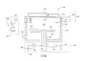
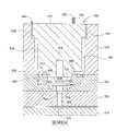
第3圖係本發明設備300的側視圖,用以實踐本文所述製程。處理腔室300的特徵在於腔室主體302、設於腔室主體302內的基材支撐件304和蓋組件306,蓋組件306耦接至腔室主體302並圍住處理容積320內的基材支撐件304。經由開口326提供基材至處理容積320,開口326傳統上由門板密封以進行處理。Figure 3 is a side view of an
電極308設置鄰接腔室主體302,且隔開腔室主體302與蓋組件306的其他部件。電極308可為蓋組件306的一部分,或為分離的側壁電極。電極308可為環狀或環形構件,且可為環形電極。電極308可為連續迴路環繞處理腔室300周圍而圍繞處理容積320,或可依需求在選定位置係不連續的。電極308亦可為穿孔電極,例如穿孔環或網狀電極。電極308亦可為平板電極,例如次要氣體分配器。
隔離器310可為介電材料,例如陶瓷或金屬氧化物,例如氧化鋁及/或氮化鋁,隔離器310接觸電極308,並電氣與熱隔開電極308和氣體分配器312與腔室主體302。氣體分配器312的特徵在於開口318,以供製程氣體進入處理容積320。氣體分配器312可耦接至電源342,例如RF產生器。亦可採用DC功率、脈衝式DC功率和脈衝式RF功率。
氣體分配器312可為導電氣體分配器或非導電氣體分配器。氣體分配器312亦可由導電與非導電部件組成。例如,氣體分配器312的主體可具導電性,氣體分配器312的面板則不導電。在電漿處理腔室中,如第3圖所示,可供電給氣體分配器312,或者氣體分配器312可接地。The
電極308可耦接至調諧電路328,以控制處理腔室300的接地途徑。調諧電路328包含電子感測器330和電子控制器334,電子控制器334可為可變電容。調諧電路328可為包含一或更多電感332的LLC電路。調諧電路328可為任一電路,電路特徵為在處理期間,可在處理容積320存有電漿條件下改變或控制阻抗。在第3圖實施例中,調諧電路328的特徵在於與電子控制器334串聯的第一電感332A和與電子控制器334並聯的第二電感332B。電子感測器330可為電壓或電流感測器,且可耦接至電子控制器334,以提供一定程度的閉環控制處理容積320內的電漿條件。
第二電極322可耦接至基材支撐件304。第二電極322可埋設在基材支撐件304內或耦接至基材支撐件304的表面。第二電極322可為平板、穿孔平板、網格、絲網或任何其他分散配置。第二電極322可為調諧電極,且可由導管346耦接至第二調諧電路136,例如具選定電阻(例如50歐姆(Ω))的電纜,導管346置於基材支撐件304的軸桿344。第二調諧電路336具有第二電子感測器338和第二電子控制器340,電子控制器340可為第二可變電容。第二電子感測器338可為電壓或電流感測器,且可耦接至第二電子控制器340,以進一步控制處理容積320內的電漿條件。The
第三電極324可為偏壓電極及/或靜電夾持電極,第三電極324可耦接至基材支撐件304。第三電極可經由濾波器348耦接至第二電源350,濾波器348可為阻抗匹配電路。第二電源350可為DC功率、脈衝式DC功率、RF功率、脈衝式RF功率或上述功率組合物。The
第3圖的蓋組件306和基材支撐件304可配合任一處理腔室使用,以進行電漿或熱處理。有益使用蓋組件306和基材支撐件304的電漿處理腔室一例為取自位於美國加州聖大克勞拉市的應用材料公司(Applied Materials, Inc.)的PRODUCER®平臺與腔室。取自其他製造業者的腔室亦可配合上述部件使用。The
操作時,處理腔室300即時控制處理容積320內的電漿條件。基材放在基材支撐件304上,製程氣體依任一預定流動規劃由進口314流過蓋組件306。氣體由出口352離開腔室300。電源耦接至氣體分配器312,以於處理容積320內產生電漿。若有需要,可利用第三電極324,使基材遭受電偏壓。In operation, the
在處理容積320中激發電漿後,電漿與第一電極308間即產生電位差。電漿與第二電極322間亦會產生電位差。電子控制器334、340接著用於調整接地路徑的流動性,接地路徑係以二調諧電路328、336表示。將設定點傳遞到第一調諧電路328和第二調諧電路336,以個別控制從中心到邊緣的沉積速率和電漿密度均勻性。在電子控制器均為可變電容的實施例中,電子感測器可調整可變電容,以個別最大化沉積速率及最小化厚度不均勻性。After the plasma is excited in the
調諧電路328、336各具可變阻抗,阻抗可分別利用電子控制器334、340調整。若電子控制器334、340為可變電容,則視電漿的頻率與電壓特性而定,各可變電容的電容範圍和電感332A、332B的電感乃選擇以提供使各可變電容有最小電容範圍的阻抗範圍。故當電子控制器334的電容為最小值或最大值時,電路328的阻抗很高,導致電漿形狀以最小面積覆蓋基材支撐件。當電子控制器334的電容近似使電路328有最小阻抗的值時,電漿將有最大覆蓋面積來有效覆蓋基材支撐件304的整個工作面積。當電子控制器334的電容偏離最小阻抗設定時,電漿形狀會從室壁縮小,造成覆蓋基材支撐件的面積減少。電子控制器340具有類似作用,電漿覆蓋基材支撐件的面積將隨電子控制器340的電容改變而增加及減少。
電子感測器330、338可用於調整封閉迴路的各電路328、336。視所用感測器類型而定,電流或電壓設定點可安裝於各感測器,感測器可裝配控制軟體,以決定各電子控制器334、340的調整值,從而最小化設定點偏差。依此,可於處理期間選擇及動態控制電漿形狀。應注意雖然前述電子控制器334、340係可變電容,但任何具可調特性的電子部件皆可用於提供具可調阻抗的調諧電路328、336。
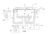
第4圖係本發明另一設備400的側視圖,用以實踐本文所述製程。第4圖的處理腔室400在許多方面類似第3圖的處理腔室300,二圖中相同的元件以相同的元件符號表示。處理腔室400的特徵在於不同的調諧電路402,調諧電路402耦接至基材支撐件304。調諧電路402具有和調諧電路328一樣的部件,即電子控制器340、電子感測器338、與電子控制器340串聯的第一電感404和與電子控制器340並聯的第二電感406。FIG. 4 is a side view of another
第4圖調諧電路402的運作方式類似第3圖的調諧電路336,但調整可變部件340時,有不同的阻抗特性。視選定電感404、406的電感而定,調諧電路402的阻抗不同於調諧電路336。故施加至基材支撐件的調諧電路特性不僅可藉由選擇可變電容來調整,可變電容的電容範圍會產生有益電漿特性的電阻範圍,還可藉由選擇電感來修改使用可變電容可獲得的阻抗範圍而調整。因具調諧電路336,可變電容340可調整通過基材支撐件的接地路徑阻抗、改變電極322的電位,及改變處理容積320內的電漿形狀。The
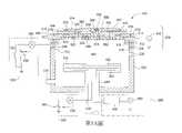
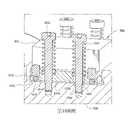
第5A圖係本發明又一設備500的側視圖,用以實踐本文所述製程。處理腔室500的特徵在於腔室主體502、設於腔室主體502內的基材支撐件504和蓋組件506,蓋組件506耦接至腔室主體502並圍住處理容積520內的基材支撐件504。經由開口526提供基材至處理容積520,開口526傳統上由門板密封以進行處理。Figure 5A is a side view of yet another
蓋組件506包含電極508,電極508設置鄰接腔室主體502,且隔開腔室主體502與蓋組件506的其他部件。電極508可為環狀或環形構件,且可為環形電極。電極508可為連續迴路環繞處理腔室500周圍而圍繞處理容積520,或可依需求在選定位置係不連續的。一對隔離器510、512接觸電極508,並電氣與熱隔開電極508和導電氣體分配器514與腔室主體502,隔離器510、512可為介電材料,例如陶瓷或金屬氧化物,例如氧化鋁及/或氮化鋁。The
隔離器510可為內部隔離器,隔離器510接觸處理容積520的處理環境,隔離器512可為外部隔離器,隔離器512不接觸處理容積520的處理環境。在此實施例中,內部隔離器的材料耐熱性或熱穩定性比外部隔離器更佳。內部隔離器可包含複數個和介面一起裝配的部件,以減緩內部隔離器中的熱應力。例如,三個陶瓷環可構成內部隔離器。若內部隔離器具耐熱性,則外部隔離器可為較不耐熱的材料,例如塑膠。若隔離器510係內部隔離器而在處理環境中提供穩定性,則隔離器510可依需要往下延伸到隔離器512的下面旁而阻隔處理環境。或者,隔離器512的下面可由和隔離器510的材料一樣或類似的隔離器取代。
在導電氣體分配器514係導電面板的實施例中,導電面板可為厚度實質均勻的平面導電類平板構件,導電面板的表面實質平行基材支撐件504的上表面。導電面板可為金屬,例如鋁或不銹鋼,在一些實施例中,可塗覆上介電材料,例如氧化鋁或氮化鋁。In the embodiment in which the
導電氣體分配器514可為導電面板,並熱接觸且可物理接觸加熱器516。加熱器516包括加熱元件576,加熱元件576可為電阻元件(例如散熱用電導體)或導電元件(例如加熱流體用導管)。導電氣體分配器514的特徵在於開口518,以供製程氣體進入處理容積520。導電氣體分配器514的邊緣部分580可沿處理腔室500的側邊進入,以將導電氣體分配器514耦接至電源542,例如RF產生器。亦可採用DC功率、脈衝式DC功率和脈衝式RF功率。The
分區阻斷板包含第一區板552和第二區板558,分區阻斷板接觸導電氣體分配器514,及提供多個氣體途徑通過蓋組件506。雖然第5A圖所示實施例係圖示分區阻斷板構造一例,但也可採用其他分區阻斷板構造,包括具有超過兩個區板的構造。第一區板552具有一或更多氣室554,供製程氣體循環通過第一途徑,而經由第一區板552的開口556分配到處理容積520,開口556流體連通導電氣體分配器514的開口518。第二區板558亦具有一或更多氣室560,供製程氣體循環通過第二途徑,而經由第二區板的開口578分配到處理容積520,開口578流體連通第一區板552的貫穿開口562和導電氣體分配器514的開口518。The partitioned blocker plate includes a
氣帽564設置接觸第二區板558,及提供入口讓製程氣體分別流入第一區板552的氣室554和第二區板558的氣室560,以於抵達處理容積520前,在不互相接觸的情況下,使製程氣體流到處理容積520。氣帽564的特徵為亦包括入口566,入口566流體連通第二區板558和第一區板552的貫穿開口568,且入口566與其中一個開口518流體連通,可依需求供製程氣體經由第三氣體途徑直接流入處理容積520。氣帽564的特徵為亦包括導管570讓流體循環通過氣帽564。流體可為熱控制流體,例如冷卻流體。水為可用冷卻流體一例,但也可使用其他流體、液體和固體。熱控制流體經由進口572提供至導管570並經由出口574抽出導管570。氣帽564熱連通第一與第二區板552、558和導電氣體分配器514。加熱器516和熱控制氣帽564一起熱控制導電氣體分配器514,以提供從邊緣到中心和基材到基材間的溫度均勻性。氣體經由入口578排出處理容積520,入口578可耦接至真空源(未圖示),真空源可沿著腔室主體設在任一便利位置且可依需求連接泵抽氣室。The
電極508可耦接至調諧電路528,以控制處理腔室500的接地途徑。調諧電路528包含電子感測器530和電子控制器534,電子控制器534可為可變電容。調諧電路528可為包含一或更多電感532的LLC電路。電子感測器530可為電壓或電流感測器,且可耦接至電子控制器534,以提供一定程度的閉環控制處理容積520內的電漿條件。
第二電極522可耦接至基材支撐件504。第二電極522可埋設在基材支撐件504內或耦接至基材支撐件504的表面。第二電極522可為平板、穿孔平板、網格、絲網或任何其他分散配置。第二電極522可為調諧電極,且可由導管546耦接至第二調諧電路536,例如具選定電阻(例如50 Ω)的電纜,導管546置於基材支撐件504的軸桿544。第二調諧電路536具有第二電子感測器538和第二電子控制器540,電子控制器540可為第二可變電容。第二電子感測器538可為電壓或電流感測器,且可耦接至第二電子控制器540,以進一步控制處理容積520內的電漿條件。The
第三電極524可為偏壓電極,且可耦接至基材支撐件504。第三電極可耦接至包含第二電源550的偏壓單元599和濾波器548,濾波器548可為阻抗匹配電路。第二電源550可為DC功率、脈衝式DC功率、RF功率、脈衝式RF功率或上述功率組合物。The
第5A圖的蓋組件506和基材支撐件504可配合任一處理腔室使用,以進行電漿或熱處理。有益使用蓋組件506和基材支撐件504的電漿處理腔室一例為取自位於美國加州聖大克勞拉市的應用材料公司的PRODUCER®平臺與腔室。取自其他製造業者的腔室亦可配合上述部件使用。The
操作時,處理腔室500即時控制蓋組件506的溫度和處理容積520內的電漿條件。基材放在基材支撐件504上,製程氣體依任一預定流動規劃流過蓋組件506。可於導電氣體分配器建立溫度設定點,並可藉由操作加熱器516及使冷卻流體循環通過導管570而控制。電力可耦合至導電氣體分配器514,以在處理容積520內產生電漿。由於導電氣體分配器514的溫度受到控制,較少電力因加熱導電氣體分配器514和蓋組件506的其他部件而耗散,故由處理腔室500處理第一基材開始,導電氣體分配器514從中心到邊緣與基材到基材間的溫度係穩定的。若有需要,可利用第三電極524,使基材遭受電偏壓。In operation, the
在處理容積520中激發電漿後,電漿與第一電極508間即產生電位差。電漿與第二電極522間亦會產生電位差。電子控制器534、540接著用於調整接地路徑的流動性,接地路徑係以二調諧電路528、536表示。將設定點傳遞到第一調諧電路528和第二調諧電路536,以個別控制從中心到邊緣的電漿密度均勻性和沉積速率。在電子控制器均為可變電容的實施例中,電子感測器可調整可變電容,以個別最大化沉積速率及最小化厚度不均勻性。電漿處理腔室可具有第一及/或第二電極。同樣地,電漿處理腔室可具有第一及/或第二調諧電路。After the plasma is excited in the
調諧電路528、536各具可變阻抗,阻抗可分別利用電子控制器534、540調整。若電子控制器534、540為可變電容,則視電漿的頻率與電壓特性而定,各可變電容的電容範圍和電感532A、532B的電感乃選擇以提供使各可變電容有最小電容範圍的阻抗範圍。故當電子控制器534的電容為最小值或最大值時,電路528的阻抗很高,導致電漿形狀以最小面積覆蓋基材支撐件。當電子控制器534的電容近似使電路528有最小阻抗的值時,電漿將有最大覆蓋面積來有效覆蓋基材支撐件504的整個工作面積。當電子控制器534的電容偏離最小阻抗設定時,電漿形狀會從室壁縮小,造成覆蓋基材支撐件的面積減少。電子控制器540具有類似作用,電漿覆蓋基材支撐件的面積將隨電子控制器540的電容改變而增加及減少。
電子感測器530、538可用於調整封閉迴路的各電路528、536。視所用感測器類型而定,電流或電壓設定點可安裝於各感測器,感測器可裝配控制軟體,以決定各電子控制器534、540的調整值,從而最小化設定點偏差。依此,可於處理期間選擇及動態控制電漿形狀。應注意雖然前述電子控制器534、540係可變電容,但任何具可調特性的電子部件皆可用於提供具可調阻抗的調諧電路528、536。
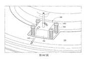
第5A圖腔室500亦具有光學量測裝置582,光學量測裝置582設於蓋組件506。光學量測裝置582通常放置在第二區板558及安座於第一區板552。蓋組件506可依需求採用不同數量的平板。光學量測裝置582通常放置在氣帽564底下的第一平板,以便於使用。光學量測裝置582光學對準穿過第一區板552的開口586。開口586對準且光學配準導電氣體分配器514的氣流開口518。通常,此類開口係設置穿過光學量測裝置582與導電氣體分配器514間的所有平板。導電氣體分配器514的開口518按尺寸製作以得氣流均勻性。光學量測裝置582產生光束,光束按尺寸產生以行經開口518,而不需重新調整開口518的尺寸。光學量測裝置582發射的光經由開口584、586、518朝基材支撐件504行進。光自置於基材支撐件504上的基材反射,及經由開口518、586、584返回光學量測裝置582。光學量測裝置582的細節將參照第9A圖至第10C圖進一步說明於後。氣帽564的凹部容納光學量測裝置582的上部,上部突出第二區板558。The
第5B圖係根據另一實施例,處理腔室590的截面示意圖。第5B圖的處理腔室590在許多方面類似第5A圖的處理腔室500,二圖中相同的元件以相同的元件符號表示。處理腔室590的特徵在於不同的調諧電路592,調諧電路592耦接至基材支撐件504。調諧電路592具有和調諧電路528一樣的部件,即電子控制器540、電子感測器538、與電子控制器540串聯的第一電感594和與電子控制器540並聯的第二電感596。FIG. 5B is a schematic cross-sectional view of a
調諧電路592的操作方式類似第5A圖的調諧電路536。調諧電路592具有可變阻抗,阻抗範圍由電路的電子部件性質、電極522和電漿設定。調諧電路592的至少一電子部件係可變的,以提供可控制的可變阻抗。改變調諧電路592的阻抗可控制處理容積520內的電漿密度分布。
第6圖係根據再一實施例,設備600的截面示意圖。設備600係二處理腔室602A、602B的串接單元。各處理腔室602A、602B可為任一腔室300、400、500、590。通常,腔室602A、602B係實質相同,但未必如此。在第6圖中,處理腔室602A、602B係相同的且類似第5B圖的腔室590。腔室602A、602B具有各自出口650A、650B,出口650A、650B設在各自的基材支撐件軸桿544A、544B周圍。腔室602A、602B經由共用真空管線652排空,管線652耦接至共用真空源630。設備600包含氣體輸送系統604,氣體輸送系統604輸送製程氣體至腔室602A、602B的蓋上的各氣體歧管606A、606B。氣體輸送系統604包含至少一氣源608,氣源608利用共用輸送導管610耦接共用流量控制裝置612與氣體歧管606A、606B。氣體輸送系統亦包含至少一氣源614,氣源614經由個別輸送導管618耦接個別流量控制裝置616A、616B與氣體歧管。共同控制分離氣流流動及個別控制流動可依需求更嚴密控制流到各腔室的製程氣體流量,同時維持流到各腔室的共同周遭氣體流量控制。FIG. 6 is a schematic cross-sectional view of an
控制器620耦接至設備600的各種控制特徵結構,包括個別控制裝置614、共用控制裝置612、各腔室的加熱器516、調諧電路的電子感測器530、538,藉以控制各調諧電路阻抗、各腔室的光學量測裝置582和各腔室的偏壓產生電路599。控制器620利用光學量測裝置582來監測沉積進行,及調整氣流、電漿密度分布和各導電氣體分配器的溫度,以達預定沉積均勻性。
第7圖係根據另一實施例,設備700的上視圖。設備700係處理腔室集合,所有腔室可為第5A圖處理腔室500的實施例,並且耦接至移送室708和負載鎖定組件704。亦可採用第5B圖處理腔室590、第3圖處理腔室300和第4圖處理腔室400。處理腔室500通常群集成串接單元702,例如第6圖串接單元600,每一處理腔室500具有單一製程氣體供應器712。如第6圖所述,製程氣體可共同控制流入設備700的串接單元600的二腔室,及/或個別控制流入串接單元600的各腔室。串接單元702設置環繞移送室708,移送室708通常具有機器人710,用以操縱基材。負載鎖定組件704的特徵在於二負載鎖定室706,二負載鎖定室706亦串接排列。設備700通常適合在高產量的製造環境中實踐本文所述方法。應注意所述任一腔室實施例、設備300、400、500或590皆可以任何組合方式用於設備700。FIG. 7 is a top view of an
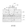
第8A圖係具多區加熱器的基材支撐件802的截面示意圖,基材支撐件802可配合本文所述其他設備和方法使用,以控制置於基材支撐件802上的基材溫度分布。基材支撐件802具有埋設熱耦804。基材支撐件802的一實施例可由熱壓燒結製程製作,其中粉狀氮化鋁(AlN)經壓製成模及加熱。在示例性實施例中,基材支撐件802的形成為將AlN粉末層疊成模而形成第一AlN層、把第一加熱元件814放置到第一AlN層上,加熱元件814可為電阻式加熱元件、沉積第二AlN粉末層至第一加熱元件814上、把第二加熱元件816放置到第二AlN粉末層上、增設第三AlN粉末層至第二加熱元件816上、把熱耦804放置到第三AlN層上,接著沉積第四AlN粉末層至熱耦804上。注意此程序會以與第8A圖顛倒的位置形成基材支撐件802。8A is a schematic cross-sectional view of a
若包括上述電極,則上述層疊製程可於加熱元件814、816和熱耦804前或後擴展,以提供偏壓電極和調諧電極。一旦AlN粉末層、加熱元件814、816、熱耦804和任何預定電極置於適當位置,即可施加高壓和高溫(此領域所熟知)至結構而進行燒結。如第8A圖所示,依此可形成實心基材支撐件802。注意以上實例係描述形成具二區之基材支撐件的步驟。在其他實施例中,可以適當對應層疊步驟和附加加熱元件與熱耦來製作具3、4、5、6或更多區之基材支撐件。If the electrodes described above are included, the lamination process described above can be extended either before or after the
在一些實施例中,熱耦804包括第一材料長條片806和第二材料長條片808。第一材料和第二材料的熔點通常夠高,以免在上述製造製程期間損壞,西白克(Seebeck)係數差異為足以產生對應小溫度變化的電壓訊號,熱膨脹係數則接近基材支撐件材料,故熱耦804或基材支撐件802不會在溫度循環時遭熱應力損壞。In some embodiments,
第一材料806和第二材料808可塑形成棒、線、帶或任何其他可行形狀,以從基材支撐件802的中心徑向延伸到基材支撐件802的外部加熱區,並且兩端有足夠的表面積來形成可靠的電氣連接。於長條片806、808的接面端810,長條片806、808可焊接在一起及/或利用導電填料連接。The
在焊接形成熱耦接面810的實施例中,焊接應選擇能讓接面810保持完整無缺,又可忍受燒結製程期間施加的熱。例如,鎢極鈍氣(TIG)焊接或類似技術可用於焊接一片W5Re、W26Re或其他導電材料與W5Re、W26Re長條片806、808,以形成焊接接面,燒結時,焊接接面不會熔化。In embodiments where the
故在一些實施例中,形成熱耦接面810的方法為將填料夾設在W5Re與W26Re帶之間,W5Re與W26Re帶用作長條片806、808。填料可為電阻不比W5Re或W26Re高且熔點高於燒結溫度的金屬。適合配合做為長條片806、808的W5Re與W26Re帶使用的填料實例包括W5Re、W26Re、鎢(W)、鉬(Mo)和類似材料。在一些實施例中,熱壓燒結製程可用於接合填料和W5Re與W26Re長條片806、808。Therefore, in some embodiments, the method of forming the
絕緣材料可插入長條片806、808間的空間812,或可將AlN粉末推進片806、808間的空間812。若AlN用於互相隔絕熱耦片806、808,則至少0.5 mm的AlN厚度通常已足夠。可採用附加厚度。注意雖然第7圖所示長條片806、808係互相堆疊於上,但在其他實施例中,長條片806、808彼此係側向隔開而置於基材支撐件802內的相同垂直位置。此配置有助於在製造期間,沉積絕緣AlN粉末至片806、808間的空間812。Insulating material may be inserted into the
第8B圖係具附加特徵結構的多區基材支撐件800的截面示意圖。燒結第8A圖的基材支撐件802後,在基材支撐件802的下表面824中心開孔818、820。孔818、820延長而露出長條片806、808。可採用任何可行的方法在基材支撐件802中開孔(例如鑽孔)。孔818、820的直徑乃製作成足以讓連接器(例如導線)連接至長條片806、808。在一些實施例中,分別用於長條片806、808的材料同樣可用於連接器。在一些實施例中,連接器的材料不同於長條片806、808。在此情況下,測量溫度將以熱耦接面810位置與基材支撐件802中心的連接器連接點間的溫差為基礎。就雙區支撐件而言,連接器連接點靠近習知用於測量內區溫度的熱耦826,熱耦826設在基材支撐件802的中心。假設連接器連接點溫度和內區溫度一樣,則可計算熱耦接面810位置的溫度。Figure 8B is a schematic cross-sectional view of a
在一些實施例中,連接器經硬焊、焊接或軟焊至長條片806、808。硬焊製程可在無氧環境中進行,以免材料氧化。此外,可開孔824使習用熱耦826插入內部加熱區的基材支撐件802。注意雖未圖示,但亦可開連接器至加熱元件814、816的附加孔,以連接元件814、816。In some embodiments, the connectors are brazed, welded or soldered to the
軸桿822接著附接至基材支撐件802的下表面828中心。在一些實施例中,軸桿822收納長條片806、808的連接器、習用熱耦826的連接器和加熱元件814、816的連接器,軸桿822可於各種連接器附接至各熱耦826、804和加熱元件814、816前,附接至基材支撐件802。The
第8C圖圖示第8B圖的多區基材支撐件800,基材支撐件800設於處理腔室,例如處理腔室502。熱耦826、804和加熱元件814、816的連接器耦接至控制器832,控制器832包括處理器和適當電路,電路適於接收及記錄來自熱耦826、804的訊號,及施加電流至加熱元件814、816。第8B圖的多區基材支撐件800可設於任一腔室300、400、500及/或590,如上所述,基材支撐件800亦可包括偏壓電極和調諧電極。FIG. 8C illustrates the
第9A圖係根據一實施例,穿過光學量測裝置582中心的截面示意圖。第9B圖係穿過第9A圖光學量測裝置582中心的截面特寫圖。如圖所示,量測裝置582包括準直儀912,準直儀912安置在第二區板558的開口940內。在第9A圖實施例中,量測裝置582延伸到選擇性座板942中並置於第一區板552與第二區板558之間。座板942亦可為區板,或者,座板942可只讓氣體在第一區板552與第二區板558間流動。第一區板552內設有窗口902,以防止製程氣體流入準直儀912而損壞準直儀912內的光學元件。窗口902可為任何能使準直儀912的光穿過第一區板552的材料,例如藍寶石、石英或具任何適當組成的玻璃。FIG. 9A is a schematic cross-sectional view through the center of the
開口940和準直儀912一同定義第一間隙934和第二間隙936。第一間隙934圍繞準直儀912的第一部分944,第二間隙936圍繞準直儀912的第二部分946。準直儀912的第一部分944可呈圓柱形,第二部分946可呈箱形。第一間隙934可大於第二間隙936,以供準直儀912傾斜或轉動,此將進一步詳述於後。
窗口902由窗口托架904托在座板942的凸耳914上。處理時,窗口902設置與基材夾一角度。操作時,光源(未圖示)經由光纖束(未圖示)提供光(通常係廣譜光,例如氙燈光)至準直儀912。光通過準直儀912,準直儀912含有光學器件,光學器件對準光和開口586、518,及把光直徑壓縮成實質為開口586、518的直徑內。光接著通過窗口902、座板942的開口950、開口586和穿過導電氣體分配器514的開口518,以照射基材。光接著自基材反射且經由開口518、586、950返回準直儀912。窗口902乃傾斜設置,以免光從準直儀912直接向外反射回準直儀912。視情況而定,使窗口902傾斜,故角度可為介於約0度至約25度的任何角度,例如約1度至約10度,例如約3度。自基材反射的光從準直儀經過光纖束(未圖示)而至光譜儀或其他光譜光分析儀(例如光電二極體、光電二極體陣列或CCD陣列)。The
利用上述結構,可於基材處理期間進行量測。出自準直儀912的光(和自基材反射的光)通過開口518時,可使氣體流過開口518,及處理基材。開口518按尺寸製作以得通過導電氣體分配器514的氣流均勻性,故尺寸通常類似導電氣體分配器514未用於原位量測的開口518。在一實施例中,開口518的直徑為0.0028”。With the above structure, measurement can be performed during substrate processing. When light from the collimator 912 (and light reflected from the substrate) passes through the
光經由導管930進入準直儀912,導管930具有複數個光纖932而形成光纖束。準直儀912的特徵在於光學器件(未圖示),例如透鏡和鏡子,以將光從光纖束932重新引導到準直儀912的開口948。光學器件對準從準直儀912通過開口948的光和開口950、586、518,及聚焦或塑造光形狀,使光配適通過最小尺寸的開口950、586、518。沿著垂直平面的路徑引導光,該平面由基材的二直徑構成,使光實質垂直基材表面。光學器件亦塑造光形狀,使自基材表面反射的光亦實質通過開口518、586、950而至準直儀912,且經由光纖束932離開而至光譜光分析儀。Light enters the
光纖束可用於從單一寬頻源傳遞光到如第6圖及第7圖實施例所示多個腔室。單一光源可傳遞光至光纖束內,束中一些光纖繞徑至各腔室,使不同腔室中的測量光係均勻且盡可能相同。如此可減少潛在測量誤差來源或變異。在一情況下,七個一束的光纖由一個光源照射,三個光纖則繞徑至二不同處理腔室各自的三個準直儀。七個光纖直接繞徑至光譜儀來提供參考值,藉以補償光源隨時間的變化。依此,單一光源有助於測量二不同處理腔室中晶圓上的一些位置,以提供監測二腔室同時進行的沉積製程的能力。此能力容許控制二腔室,以減少二腔室同時進行的製程變異。Fiber optic bundles can be used to deliver light from a single broadband source to multiple chambers as shown in the embodiments of Figures 6 and 7. A single light source can deliver light into a bundle of optical fibers, some of which are routed to each chamber, so that the measurement light system in the different chambers is uniform and as identical as possible. This reduces potential sources of measurement error or variability. In one case, a bundle of seven fibers was illuminated by one light source, and three fibers were routed to three collimators in each of two different processing chambers. Seven fibers are routed directly to the spectrometer to provide reference values to compensate for changes in the light source over time. Accordingly, a single light source facilitates the measurement of locations on the wafer in two different processing chambers, providing the ability to monitor deposition processes in the two chambers simultaneously. This capability allows control of the two chambers to reduce process variation in the simultaneous operation of the two chambers.
引導至基材的光可未極化,波長範圍可為約200 nm至約800 nm。光纖將光部分準直,使光行經氣體分配器的氣流開口,同時讓氣體流過開口,及照射晶圓上定點,定點可為任何合宜尺寸,例如直徑約0.1 mm至約5 mm,例如直徑約2 mm。The light directed to the substrate may be unpolarized and may range in wavelength from about 200 nm to about 800 nm. The optical fiber partially collimates the light, passes the light through the gas flow openings of the gas distributor, while allowing the gas to flow through the openings, and illuminates a spot on the wafer, which may be of any convenient size, such as about 0.1 mm in diameter to about 5 mm in diameter, such as about 2 mm.
可在上述任何設備進行沉積製程期間,形成電漿。出自電漿的光可由光譜儀偵測,光譜儀耦接至本文所述原位監測設備,且可能隱蔽反射結果。此作用可藉由在啟動測量光源前取得電漿光譜來補償。接著從自反射測量光接收的光譜減去電漿光譜。耦接或整合於光譜儀的控制器或電腦可從偵測反射光譜減去偵測電漿光譜,以產生校正反射光譜。校正反射光譜接著用於執行本文所述演算法。可依需求在測量光源每次閃爍前,校正電漿光譜,以補償各閃光間的電漿光譜漂移。The plasma can be formed during the deposition process of any of the above-described apparatuses. Light from the plasma can be detected by a spectrometer coupled to the in situ monitoring equipment described herein, and the reflection results may be masked. This effect can be compensated by acquiring the plasma spectrum before activating the measurement light source. The plasma spectrum is then subtracted from the spectrum received by the self-reflection measurement light. A controller or computer coupled to or integrated with the spectrometer can subtract the detected plasma spectrum from the detected reflectance spectrum to generate a corrected reflectance spectrum. The corrected reflectance spectrum is then used to execute the algorithms described herein. The plasma spectrum can be corrected before each flicker of the measurement light source to compensate for the drift of the plasma spectrum between each flicker as required.
處理時,諸如第一區板552、第二區板558、導電氣體分配器514和選擇性座板942等各種腔室部件將經歷熱膨脹及收縮。故除非準直儀912適當設置在腔室內,否則準直儀912與開口586、518很容易失準。為確保準直儀912適當對準開口586、518,準直儀912具有錐形延伸部926,錐形延伸部926具有傾斜側壁908,例如截頭錐形延伸部,以嚙合凹部922與對應座板942的傾斜壁面906,凹部922可為錐形孔。在無選擇性座板942的實施例中,凹部可形成在第一區板552中。第二區板558亦可具有傾斜壁面910,以容納延伸部926。壁面908、910和錐形延伸部926可與座板942的頂表面920夾一角度「α」。準直儀912延伸到座板942的凹部922內,故當座板942因熱膨脹/收縮而側向移動時,準直儀912可相應移動並保持適當對準開口586、518。角度「α」可為任何角度,只要能使座板942中的熱膨脹側向力量有效傳輸到準直儀912的延伸部926,又不致產生軸向力量造成準直儀912脫離凹部922即可。角度「α」通常為約100度至約145度,例如120度。During processing, various chamber components such as
導電氣體分配器514和第一區板552通常接觸到比第二區板高的溫度。在典型操作中,導電氣體分配器514可加熱達約300℃至約600℃,第二區板558遭受的溫度比導電氣體分配器514低50℃至100℃。在第一區板552和導電氣體分配器514為鋁的實施例中,第一區板552與導電氣體分配器514的膨脹差異為10 nm至100 nm,導電氣體分配器514與第二區板558的膨脹差異為200 nm至500 nm,以致準直儀912與開口940間有些微的對準變化。The
第一開口934和第二開口936按尺寸製作以當座板942移動時,準直儀912可側向移動,又不會碰到第二區板558。在一典型實施例中,若熱循環造成座板942膨脹及收縮,則準直儀912可側向移動達約0.03吋的距離,例如約0.02吋。第一與第二間隙934、936通常按尺寸製作以在準直儀912不接觸第二區板558的情況下移動。第一間隙934的尺寸可達約0.15吋,例如約0.04吋至約0.12吋,例如約0.10吋。第二間隙936的尺寸可和第一間隙934一樣高達約0.15吋,例如約0.04吋至約0.12吋。第二間隙936可小於或大於第一間隙934。在第9A圖及第9B圖實施例中,第二間隙936小於第一間隙934,例如約0.08吋。The
準直儀912的錐形延伸部926具有邊緣952,邊緣952配準凹部922。邊緣952通常會磨圓或去角,以降低準直儀912隨凹部922移動時產生微粒的機會。磨圓邊緣952在準直儀912與壁面908、910間提供滑面,以減少介面磨擦力引起微粒形成。磨圓邊緣的曲率半徑通常小於0.1”,例如約0.05”至約0.09”,例如約0.07”。The
依此配置,第9A圖及第9B圖的光學量測裝置582可於處理期間進行原位光學分析基材。出自準直儀的光通過開口518,同時製程氣體流過開口518而至腔室。可按尺寸製作供製程氣體流過的開口518,以最佳化氣流通過噴淋頭的均勻性,不需考慮量測所需尺寸,量測裝置可配適所得開口尺寸,而不會干擾氣流均勻性。With this configuration, the
第10A圖及第10C圖係用以將準直儀912裝設於第二區板558的機構等角視圖。第10B圖係穿過裝設機構的準直儀912的截面示意圖。如第10A圖所示,四個扣件1002(例如螺栓)延伸穿過準直儀912,且可拆式固定於第二區板558。在一實施例中,扣件1002包含螺栓。彈性構件1004(可為彈簧)耦接各扣件1002前端與準直儀912,如此當熱膨脹造成準直儀912移動時,準直儀912仍附接至第二區板558,並可朝箭頭「A」所指方向移動。彈性構件1004迫使準直儀912仍安座在座板942的凹部922內,如此座板942受熱應力作用而側向移動時,將促使準直儀912側向移動。導管1006收納光纖束1008且於入口1010處耦接至準直儀912。光纖束1008從光產生器(未圖示)承載光至準直儀912而投射到基材上,及自基材反射光而經由準直儀912返回光分析儀(未圖示)。FIGS. 10A and 10C are isometric views of the mechanism used to mount the
第3B圖圖示穿過準直儀912一側扣件1002繪製的準直儀912的截面透視圖。第10B圖截面平行於第9A圖及第9B圖截面,但為透視觀察。扣件1002安座於第二區板558,彈性構件1004由凸耳1022接觸準直儀912,以提供軸向力至準直儀912上而協助安置準直儀。扣件1002通過準直儀912中的開口1024。各扣件1002與各自開口1024間的間隙1026容許準直儀912相對扣件1002和相對第二區板558側向移動。間隙1026按尺寸製作以供側向移動,又不會讓準直儀912接觸扣件1002,間隙尺寸通常高達約0.15吋,例如約0.04吋至約0.12吋,例如約0.10吋。FIG. 3B illustrates a cross-sectional perspective view of the
提供球軸承1012,各球軸承1012安座於插座1014,插座1014形成在表面1016的準直儀912中,表面1016接合第二區板558的接收表面1018。各球軸承1012在各自的插座1014內旋轉,以容許準直儀912側向移動,同時最小化準直儀與第二區板558間的摩擦。插座1014具有具錐形部1020的側壁,錐形部1020朝球軸承1012逐漸變細而與表面1016間形成角度「β」,以使球軸承1012保持在插座1014內,同時容許球軸承平順轉動。角度「β」可為約40度至約80度,例如約50度至約70度,例如約60度。
操作時,第一區板552、座板942、導電氣體分配器514和第二區板558皆以RF功率電偏壓達實質相同電位。故RF板條1022用於電氣連接準直儀912與第二區板558,使準直儀912仍保持與第二區板558實質相同的電位。In operation, the
本文所述原位量測實施例可利用折射效應來測定層厚度,折射效應取決於層厚度。出自原位量測裝置的光照射基材、穿透層,及依據菲涅爾(Fresnel)方程式自層間介面差別反射。反射光與入射光和自其他層反射的光作用產生干涉圖案。干涉圖案受控於層的厚度和組成。生成層時,干涉圖案會以可預期的方式隨生成層厚度改變,故可偵測終點。生成層期間辨識的最終干涉圖案將變成特徵圖案,用以於沉積後續層期間觀察圖案隨後續層形成時的變化。The in-situ metrology embodiments described herein may utilize the effect of refraction, which is dependent on layer thickness, to determine layer thickness. The light from the in-situ measurement device illuminates the substrate, penetrates the layer, and reflects differentially from the interface between layers according to the Fresnel equation. The reflected light interacts with incident light and light reflected from other layers to create an interference pattern. The interference pattern is controlled by the thickness and composition of the layers. As the layers are generated, the interference pattern changes in a predictable manner with the thickness of the generated layer, so that endpoints can be detected. The final interference pattern identified during the generation of the layer will become the feature pattern, which is used to observe changes in the pattern as subsequent layers are formed during deposition of subsequent layers.
利用準直儀與阻斷板間的傾斜介面,即使阻斷板發生熱膨脹/收縮時,準直儀仍可保持實質對準氣體通道,氣體通道形成穿過氣體分配器。準直儀設在阻斷板內且為環形基板,即使氣體通道正在使用(即有處理/清洗氣體流貫),準直儀仍可經由氣體通道引導光及接收反射光。故可在不負面影響製程均勻性的情況下進行量測。提供不供氣體流貫的量測用通道將導致製程不均勻,此係因為通道會位於部分基材上,通道附近的氣流則因缺少氣體流過通道而不均勻。With the inclined interface between the collimator and the blocking plate, even when the blocking plate thermally expands/contracts, the collimator can remain substantially aligned with the gas channel formed through the gas distributor. The collimator is located in the blocking plate and is a ring-shaped substrate, even if the gas channel is in use (ie, there is processing/cleaning gas flowing through), the collimator can still guide light and receive reflected light through the gas channel. Measurements can therefore be performed without adversely affecting process uniformity. Providing measurement channels that do not allow gas to flow through will result in process inhomogeneity because the channels will be located on part of the substrate, and the gas flow near the channels will be non-uniform due to the lack of gas flow through the channels.
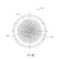
本文所述實施例的特徵在於一個原位量測裝置或構造。應注意一些實施例的特徵在於多個原位量測裝置,以即時監測基材表面複數個位置的膜形成。第11圖係第5A圖及第5B圖利用原位量測的導電氣體分配器514的底部視圖。三個開口1102環繞第11圖實施例,圖表示開口除供氣體流動外,還用於原位光學量測。分析位置可依任何預定圖案分配。在第11圖實施例中,三個原位量測裝置係分散配置。三個原位量測裝置可沿著與基材支撐件同心的圓設置,也就是說三個裝置可設置以監測三個位置,三個位置離置於基材支撐件上的基材中心實質相同距離。或者,三個原位量測裝置可設置離中心不同距離處。多個監測裝置可用於監測基材表面不同位置的沉積均勻性、厚度與組成,及達到閉環控制沉積速率和均勻性的目的,同時在腔室中沉積一層或複數個層。Embodiments described herein feature an in-situ metrology device or configuration. It should be noted that some embodiments feature multiple in-situ measurement devices to monitor film formation at multiple locations on the substrate surface in real time. FIG. 11 is a bottom view of the
上述第9A圖至第10C圖的光學量測裝置將產生光來表示基材上的層結構。已知入射光譜的光經引導垂直基材,並自基材表面反射。一些光穿過形成於基材上的層,及自層介面反射而產生反射光譜,反射光譜不同於入射光譜。沉積層期間,反射光譜會隨沉積層厚度改變而變化。比較反射光譜與入射光譜和同一層的先前反射光譜可準確測定沉積層厚度。可在基材上多個位置進行測量,以測定層厚度均勻性,及啟用校正動作來控制均勻性。此測量方式亦可用於偵測層厚度何時達目標值,從而中斷沉積。The optical measurement devices of Figures 9A to 10C described above will generate light to represent the layer structure on the substrate. Light of a known incident spectrum is directed perpendicular to the substrate and reflected from the substrate surface. Some of the light passes through the layers formed on the substrate and is reflected from the interface of the layers to produce a reflectance spectrum that is different from the incident spectrum. During deposition, the reflectance spectrum varies with the thickness of the deposited layer. Comparing the reflectance spectrum with the incident spectrum and previous reflectance spectra of the same layer can accurately determine the thickness of the deposited layer. Measurements can be made at multiple locations on the substrate to determine layer thickness uniformity and enable corrective actions to control uniformity. This measurement can also be used to detect when the layer thickness reaches a target value, thereby interrupting the deposition.
自層的二表面反射的入射光相對於入射光將呈現相位移,該層厚度可與光波長相當。相位移與膜厚有關,且會在入射光與反射光間產生特徵干涉圖案。故反射光的光譜強度取決於層厚度。若已知毗鄰下層或材料的光學性質,則單一脈衝或閃光可自頂層反射,及利用菲涅爾方程式來比較反射光與入射光,以測定頂層厚度。Incident light reflected from both surfaces of the layer will exhibit a phase shift relative to the incident light, and the thickness of the layer may be comparable to the wavelength of the light. The phase shift is related to film thickness and produces a characteristic interference pattern between incident and reflected light. The spectral intensity of the reflected light therefore depends on the layer thickness. If the optical properties of the adjacent underlying layer or material are known, a single pulse or flash can be reflected from the top layer, and the Fresnel equation is used to compare the reflected and incident light to determine the top layer thickness.
若不知毗鄰下層的光學性質,則可在沉積頂層時,使用多個閃光與脈衝光,以測定反射率隨頂層厚度的變化。沉積速率和時間可用於計算每次脈衝光時的層厚度。反射率通常係依層厚度的正弦函數變化。可用曲線擬合反射率資料,以計算毗鄰下層的反射率。若使用廣譜光源和光譜光分析儀,則亦可比較多個波長,以提高毗鄰下層的光學性質周圍的收斂性。毗鄰下層的反射率可表示為頂層反射率的函數,毗鄰下層的光學性質可利用菲涅爾方程式計算而得。If the optical properties of the adjacent underlying layers are unknown, multiple flashes and pulses of light can be used as the top layer is deposited to measure the reflectance as a function of the thickness of the top layer. The deposition rate and time can be used to calculate the layer thickness per pulse of light. The reflectivity generally varies as a sinusoidal function of the layer thickness. The reflectance data can be fitted with a curve to calculate the reflectance of adjacent sublayers. If a broad-spectrum light source and a spectroscopic light analyzer are used, multiple wavelengths can also be compared to improve convergence around optical properties adjacent to the underlying layers. The reflectivity of the adjacent lower layer can be expressed as a function of the reflectance of the top layer, and the optical properties of the adjacent lower layer can be calculated using the Fresnel equation.
若毗鄰下層經圖案化,則自毗鄰下層反射的光具有極化分量,極化分量係按根均方關係貢獻總反射強度。自基材反射的各光波長具有與其他波長無關的反射強度,各反射光波長將依據頂層和毗鄰下層的光學性質作用。故可使用計算而得的頂層厚度與已知頂層光學性質來進行多個反射波長的光譜分析,以擬合毗鄰下層反射率的極化分量和引起該等分量的毗鄰下層光學性質。If the adjacent lower layer is patterned, the light reflected from the adjacent lower layer has a polarized component that contributes to the total reflected intensity in a root-mean-square relationship. Each wavelength of light reflected from the substrate has an intensity of reflection independent of the other wavelengths, and each wavelength of reflected light will function according to the optical properties of the top layer and the adjacent lower layer. The calculated top layer thickness and known top layer optical properties can therefore be used to perform spectral analysis of multiple reflected wavelengths to fit the polarized components of the reflectivity of the adjacent underlying layers and the adjacent underlying optical properties that cause these components.
一旦測定毗鄰下層的光學性質,即可建構基材反射率的完整模型,及利用菲涅爾方程式,從單一脈衝反射光獲知沉積層厚度。若沉積多層,則可使用單一脈衝光,從已知待沉積層的光學性質和已知毗鄰下層的光學性質計算各層的反射率。或者,如上所述,可分析進行沉積時的多個脈衝,以重新建構毗鄰下層的光學性質。Once the optical properties of the adjacent underlying layers are determined, a complete model of the reflectivity of the substrate can be constructed, and the thickness of the deposited layer can be known from a single pulse of reflected light using the Fresnel equation. If multiple layers are deposited, the reflectivity of each layer can be calculated from the known optical properties of the layer to be deposited and the known optical properties of the adjacent underlying layers using a single pulse of light. Alternatively, as described above, multiple pulses as the deposition is performed can be analyzed to reconstruct the optical properties of the adjacent underlying layers.
若已知毗鄰下層的光學性質,則可根據下列方程式,擬合廣義正弦曲線與資料,而從反射率資料集R(t,λ)計算頂層厚度:
亦可利用菲涅爾方程式的差異,使待沉積層的反射率與毗鄰下層的反射率相關聯如下:


以下為使用電腦應用處理方案來施行此一般方式的示例性說明。1.輸入資料:The following is an exemplary illustration of the general manner in which this is performed using a computer application processing scheme.1.Input information:
實驗反射率資料R(λ,t)由L個波長(λ)和M個時間點(t)組成,以表示在M個時間點時,L個波長自基材的反射率。

使用模型擬合實驗資料,模型係以下列由菲涅爾方程式推導的式子表示,菲涅爾方程式控制光反射與折射性質,包括計及形成於基材上的結構極化效應的極化率。


在以上方程式中,DR,1係單一變數(非λ或t的函數),


χ2的最小化係利用迭代雷文柏格-馬括特(LM)演算法,求得線性方程式集的解:


以下以類電腦碼語言說明上述演算法,類電腦碼語言的特徵在於大部分高階電腦程式語言常見的類屬函數規格。TargetFunction(out A, out B, out χ2){Foreach p∈P, λ and t{Calc


擬合模型與具58個波長的實驗資料集時,程式化以進行上述演算法的適當配置電腦期呈現表1所列的CPU時間分配。表1- 58個波長的分析工具資料
可使用資料子集,反覆進行上述演算法,以有效收斂模型的準確擬合度。在一實例中,實驗資料由L=60個波長組成。在此實例中,可多次引用演算法如下,每次使用不同數量的擬合參數:1. 經過一段預定時距(例如M=100)後,第一次執行只涉及有限的波長數量(例如L=15),故擬合參數的數量N=15×4+1=61,包括DR,1。2. 第二步驟為就步驟1未包括的其餘波長,計算擬合參數


可利用所述任何設備,形成示例性氧化矽層如下。把基材放到處理腔室的基材支撐件上,處理腔室具有本文所述特徵結構。經由蒸發器流入1000 mgm的TEOS,並與5000 sccm的氦氣和6000 sccm的N2O混合,以形成前驅物氣體混合物。使氣體混合物流入處理腔室。應注意若使用分區噴淋頭,則可使TEOS流過某一區及使N2O流過另一區。氦氣流可分成兩份,第一份用於稀釋蒸發的TEOS或承載至第一區,第二份用於稀釋N2O或承載至第二區。An exemplary silicon oxide layer may be formed as follows using any of the apparatuses described. The substrate is placed on a substrate support in a processing chamber having the features described herein. 1000 mgm of TEOS was flowed through the evaporator and mixed with 5000 sccm of helium and 6000 sccm ofN2O to form a precursor gas mixture. The gas mixture is flowed into the processing chamber. It should be noted that if zoned showerheads are used, it is possible to allow TEOS to flow through one zone andN2O to flow through another zone. The helium flow can be split into two, the first for diluting the evaporated TEOS or loading to the first zone, and the second for diluting theN2O or loading to the second zone.
處理腔室內的壓力設為4.0托耳,腔室面板與基材的間距設為400密耳。面板溫度設為200℃。側壁調諧電極電流目標設為6 A,基材支撐件調諧電極電流目標設為1 A。基材溫度設為500℃,基材支撐件的溫度區偏差設為5℃,且外部的溫度高於內部。The pressure in the processing chamber was set at 4.0 Torr, and the spacing between the chamber panel and the substrate was set at 400 mils. The panel temperature was set to 200°C. The sidewall tuning electrode current target was set to 6 A, and the substrate support tuning electrode current target was set to 1 A. The substrate temperature was set to 500°C, the temperature zone deviation of the substrate support was set to 5°C, and the temperature of the outside was higher than that of the inside.
使功率耦合至前驅物氣體,以形成電漿。以500 W的功率施加頻率為13.56 MHz的高頻RF功率,以100 W的功率施加頻率為300 kHz的低頻RF功率。該等條件可持續一段預定時間,以沉積具預定厚度的層,厚度通常為200 Å至2000 Å。沉積氧化矽層的厚度標準差不超過約1%。故沉積層的厚度均勻性不糟於約1%。Power is coupled to the precursor gas to form a plasma. High-frequency RF power with a frequency of 13.56 MHz was applied at 500 W, and low-frequency RF power with a frequency of 300 kHz was applied at 100 W. These conditions may be continued for a predetermined period of time to deposit a layer of a predetermined thickness, typically 200 Å to 2000 Å thick. The standard deviation of the thickness of the deposited silicon oxide layer does not exceed about 1%. Therefore, the thickness uniformity of the deposited layer is not worse than about 1%.
可由本文所述另一製程實施例,使用所述設備,以矽烷做為前驅物來形成氧化矽層。矽烷流量為100 sccm,氦氣流量為3000 sccm,N2O流量為6000 sccm。間距為300密耳,壓力為3托耳,高頻功率為400 W,低頻功率為100 W,面板溫度為200℃,基材溫度為500℃,溫度區偏差為5℃(外部高於內部),側壁調諧電極電流目標為1 A,基材支撐件調諧電極電流目標為3 A。氧化矽層的形成厚度均勻性不糟於約1%。A silicon oxide layer may be formed using the apparatus using silane as a precursor from another process embodiment described herein. The silane flow was 100 sccm, the helium flow was 3000 sccm, and theN2O flow was 6000 sccm. 300 mil spacing, 3 Torr pressure, 400 W high frequency power, 100 W low frequency power,
可由本文所述又一製程實施例,使用所述設備來形成氮化矽層。矽烷流量為30 sccm,氮氣流量為3000 sccm,氨氣流量為6000 sccm,氬氣流量為1000 sccm。間距為700密耳,壓力為3托耳,高頻功率為600 W,低頻功率為200 W,面板溫度為200℃,基材溫度為500℃,溫度區偏差為5℃(外部高於內部),側壁調諧電極電流目標為7安培(A),基材支撐件調諧電極電流目標為1 A。氮化矽層的形成厚度均勻性不糟於約1%。The apparatus may be used to form a silicon nitride layer by yet another process embodiment described herein. The silane flow was 30 sccm, the nitrogen flow was 3000 sccm, the ammonia flow was 6000 sccm, and the argon flow was 1000 sccm. 700 mil spacing, 3 Torr pressure, 600 W high frequency power, 200 W low frequency power,
可由本文所述再一製程實施例,使用所述設備來形成氮化矽層。矽烷流量為150 sccm,氮氣流量為6000 sccm,氨氣流量為1000 sccm。間距為700密耳,壓力為4托耳,高頻功率為600 W,低頻功率為200 W,面板溫度為200℃,基材溫度為500℃,溫度區偏差為5℃(外部高於內部),側壁調諧電極電流目標為6 A,基材支撐件調諧電極電流目標為1 A。氮化矽層的形成厚度均勻性不糟於約1%。The apparatus may be used to form a silicon nitride layer by yet another process embodiment described herein. The silane flow was 150 sccm, the nitrogen flow was 6000 sccm, and the ammonia flow was 1000 sccm. 700 mil spacing, 4 Torr pressure, 600 W high frequency power, 200 W low frequency power,
可由本文所述另一製程實施例,使用所述設備來形成摻雜的無定形矽層。矽烷流量為500 sccm,氦氣流量為10000 sccm,摻質前驅物(例如TMB、硼烷及/或膦,稀釋成在氦氣中的濃度為95%)的流量為500 sccm。間距為300密耳,壓力為10托耳,高頻功率為300 W,無施加低頻功率,面板溫度為175℃,基材溫度為500℃,溫度區偏差為0℃,側壁調諧電極電流目標為6 A,基材支撐件調諧電極電流目標為3 A。摻雜的無定形矽層的形成厚度均勻性不糟於約1%。The apparatus may be used to form a doped amorphous silicon layer by another process embodiment described herein. The silane flow was 500 sccm, the helium flow was 10,000 sccm, and the flow rate of dopant precursors (eg, TMB, borane and/or phosphine, diluted to 95% in helium) was 500 sccm. 300 mil spacing, 10 Torr pressure, 300 W high frequency power, no low frequency power applied, panel temperature 175°C,
可調整某一配方至下一配方的腔室條件,以相繼製作諸如上述層的層堆疊。若期產生鮮明介面,則可中斷氣流及在各配方間淨化腔室。或者,可線性改變某一配方至下一配方的腔室條件,同時持續沉積以製作漸變介面。The chamber conditions from one recipe to the next can be adjusted to sequentially make layer stacks such as those described above. If a distinct interface is desired, the airflow can be interrupted and the chamber cleaned between formulations. Alternatively, the chamber conditions from one formulation to the next can be changed linearly while deposition continues to create a graded interface.
上述原位監測演算法可用於監測堆疊中的各層厚度,例如氧化矽與氮化矽交替堆疊或多晶矽與氧化矽交替層。在各情況下,於堆疊開始沉積層時,即施行採用毗鄰下方材料反射率的演算法,以追蹤下層反射率隨層沉積時的變化。The in-situ monitoring algorithm described above can be used to monitor the thickness of layers in a stack, such as alternating layers of silicon oxide and silicon nitride or alternating layers of polysilicon and silicon oxide. In each case, when the stack begins to deposit layers, an algorithm is performed that uses the reflectivity of the adjacent underlying material to track the change in reflectivity of the underlying layer as the layer is deposited.
茲發現包括多晶矽層的層堆疊可能因多晶矽在較短波長下具高度吸收本質而遵循一簡化方式。例如,當形成多晶矽與氧化矽層交替堆疊時,毗鄰下層於波長小於約600 nm時的反射率影響明顯達到表面以下三層,但不會超過。在此結構中,觀察到波長小於約600 nm時,取自10個多晶矽/氧化矽層交替堆疊的反射光譜與取自形成第四對層後的相同堆疊光譜重疊。此相同行為與第一層無關(即無論第一層為多晶矽或氧化物)。故一有效方式包括在沉積前三對層(前六層)期間,擬合反射率資料與時序模型,然後假定毗鄰下層反射率在較短波長下為非時變,及採用波長序列擬合程序。It has been found that layer stacks comprising polysilicon layers may follow a simplified approach due to the highly absorbing nature of polysilicon at shorter wavelengths. For example, when alternating stacks of polysilicon and silicon oxide layers are formed, the reflectivity effect of the adjacent underlying layers at wavelengths less than about 600 nm significantly reaches three layers below the surface, but does not exceed. In this structure, it was observed that at wavelengths less than about 600 nm, the reflectance spectra taken from the alternating stack of 10 polysilicon/silicon oxide layers overlapped with the spectra taken from the same stack after forming the fourth pair of layers. This same behavior is independent of the first layer (ie whether the first layer is polysilicon or oxide). Therefore, an effective approach involves fitting the reflectivity data to the time-series model during the deposition of the first three pairs of layers (the first six layers), then assuming that the reflectivity of the adjacent underlying layers is time-invariant at shorter wavelengths, and using a wavelength sequence fitting procedure. .
上述方法可用於測定形成於基材上的膜厚,基材具有未知性質。在習知反射儀中,基材乃完全知悉,已知的基材性質用於折射模型化,以測定膜厚。然在許多情況下,無法預先知道基材性質,故不能使用習知反射儀。利用本文所述設備和方法,可由膜形成期間收集的時序資料推斷基材性質。在膜沉積期間按100微秒時距收集反射光譜而提供資料,擬合該資料與所述模型,以從中抽出基材性質。藉由擬合所述時序資料與菲涅爾方程式模型,可測定基材性質、實部與虛部折射率、基材的s與p反射率和膜沉積速率,該等性質接著可用於測定後續沉積的膜厚。The methods described above can be used to determine the thickness of films formed on substrates having unknown properties. In conventional reflectometers, the substrate is fully known and known substrate properties are used for refraction modeling to determine film thickness. However, in many cases, the properties of the substrate cannot be known in advance, so conventional reflectometers cannot be used. Using the apparatus and methods described herein, substrate properties can be inferred from time series data collected during film formation. Reflectance spectra were collected at 100 microsecond intervals during film deposition to provide data that were fitted to the model to extract substrate properties therefrom. By fitting the time series data to a Fresnel equation model, substrate properties, real and imaginary refractive indices, substrate s and p reflectivity, and film deposition rates can be determined, which can then be used to determine subsequent Deposited film thickness.
第14A圖至第14D圖係在圖案化基材上沉積500 Å的氮化矽層期間,一些選定波長下的時序反射比資料曲線圖。第14A圖係反射分率1402對時間1404(單位:秒)的曲線圖1400。反射比資料1406係在波長230 nm下獲得,膜的模型擬合資料標為1408。可由所述演算法計算擬合,以利用時序光譜反射比資料來測定未知的基材性質。第14B圖係在波長350 nm下收集的類似資料曲線圖1410。第14C圖係在波長500 nm下收集的類似資料曲線圖1420。第14D圖係在波長700 nm下收集的類似資料曲線圖1430。Figures 14A-14D are plots of time-series reflectance data at some selected wavelengths during deposition of a 500 Å silicon nitride layer on a patterned substrate. Figure 14A is a
若第一沉積層不是很厚,則在一些情況下,時序資料中的相位移資訊可能不夠充分來準確測定基材反射率,以致測定後續層厚度時產生誤差。在此情況下,藉由收集超過一層沉積膜的時序資料,可改善準確度。例如,收集第一層膜的時序資料後,可收集第二層沉積膜的時序資料,以提供更多資料來提升模型擬合品質。第15圖係在沉積三個連續層期間,在210 nm下收集的反射分率1502對時間1504的時序擬合曲線圖1500。第一氮化物層的沉積資料標為1506。第一氧化物層的沉積資料標為1508。第二氮化物層的沉積資料標為1510。資料顯示層間介面1512、1514的某些異常特性。進行多層擬合時,此類異常現象可由任何合宜手段移除,例如統計或手動方式。If the first deposited layer is not very thick, in some cases, the phase shift information in the time series data may not be sufficient to accurately determine the substrate reflectivity, resulting in errors in determining the thickness of subsequent layers. In this case, accuracy can be improved by collecting timing data for more than one deposited film. For example, after collecting the timing data of the first layer of film, the timing data of the second layer of deposited film can be collected to provide more data to improve the model fitting quality. Figure 15 is a time series
第16A圖係表面具未知圖案的基材的反射分率1602對波長1604(單位:奈米)的曲線圖1600。利用時序分析結果來進行擬合,以擬合未知的基材參數。實際反射比資料標為1606,擬合資料標為1608。第16B圖圖示沉積第一層氮化物層至基材上後的類似相同堆疊資料。第16C圖圖示沉積第十二層氧化物層後的類似相同堆疊資料,第16D圖圖示沉積第24層氮化物層後的類似相同堆疊資料。Figure 16A is a
擬合諸如第16A圖至第16D圖所示光譜與膜模型方程式,可測定膜厚。第17A圖係與氧化矽層交替堆疊沉積24層氮化矽層後,相較於以穿透式電子顯微鏡所得厚度測量值1708,由反射比1706測量的層厚度1702(單位:Å)對層數量1704的曲線圖1700。第17B圖圖示相同堆疊中的氧化物層的類似資料。如第17A圖及第17B圖所示,即使堆疊變厚,二者仍相當一致。然應注意隨著堆疊變厚,由於所述遞迴方法的複合誤差,TEM測量值與反射比測量值間的一致性將下降。Fitting spectra such as those shown in Figures 16A to 16D to the film model equations, the film thickness can be determined. Figure 17A shows the layer thickness measured by reflectance 1706 (unit: Å) of 1702 (unit: Å) for the
模型化及解得基材性質涉及的計算可能很密集。如上所述,管理計算時間使計算不會嚴重落後層形成的方法包括在擬合較慢的時序資料時,緩衝電腦記憶體中的資料,接著在使用靜態模型來計算後續層時,讓電腦「趕上」。在其他態樣中,可平行使用多個處理單元,例如將資料依據時間切面或頻率分組,及同時以不同處理器處理不同組。依此可指派資料組給負載較少的處理器,以均衡負載。The computation involved in modeling and solving for substrate properties can be intensive. As mentioned above, ways to manage computation time so that computation does not lag significantly behind layer formation involves buffering the data in the computer's memory when fitting slower time series data, and then letting the computer "" catch up". In other aspects, multiple processing units can be used in parallel, such as grouping data according to time slices or frequency, and processing different groups simultaneously with different processors. In this way, data sets can be assigned to less loaded processors to balance the load.
在一些實施例中,若容許較不準確的基材性質測定,則可只用選定光譜波長或選定時間切面來進行時序擬合。若某些波長受到光譜儀解析度的不當影響,則分析時可排除該等波長。In some embodiments, only selected spectral wavelengths or selected temporal slices may be used for timing fitting if less accurate substrate property determinations are tolerated. Certain wavelengths can be excluded from the analysis if they are unduly affected by the resolution of the spectrometer.
在沉積高度吸收膜的實施例中,可利用隨波長變化的不透明性,以其他手段交叉檢核厚度測定。由於材料的吸收度通常係已知波長函數,故可於膜生成時,藉由注意選定波長從反射光譜消失而標記膜厚。在此類實施例中,可選擇達目標膜厚時會從反射光譜消失的光波長,及當波長從反射光譜消失時,標記時間,以測定沉積終點。當接收此訊號時,可中斷沉積。In embodiments where highly absorbing films are deposited, the wavelength-dependent opacity can be used to cross-check thickness measurements by other means. Since the absorbance of a material is usually a known function of wavelength, the film thickness can be marked by noticing the disappearance of selected wavelengths from the reflection spectrum as the film is formed. In such embodiments, the wavelength of light that disappears from the reflection spectrum when the target film thickness is reached can be selected, and the time when the wavelength disappears from the reflection spectrum is marked to determine the deposition endpoint. When this signal is received, deposition can be interrupted.
在一些涉及吸收膜的情況下,一些層沉積至基材上後,底下基板的反射比可能會消失。在此情況下,可反覆進行時序製程,以重新描繪相繼沉積膜於上的基材特徵。可在整體沉積製程的任何合宜時刻,反覆進行時序資料擬合,以更新基材性質。In some cases involving absorber films, the reflectance of the underlying substrate may disappear after some layers are deposited onto the substrate. In this case, the sequential process can be repeated to re-delineate the features of the substrate on which the films were deposited successively. The time series data fitting can be iteratively performed at any convenient time in the overall deposition process to update the substrate properties.
在一些態樣中,基材反射比隨膜厚變化在一些波長下較激烈,在其他波長下則沒那麼激烈。在一些情況下,可測定反射光譜的敏感函數及集中計算對膜厚最敏感的波長,以有效使用計算資源。例如,若收集時序,則可快速分析前十個抽點或任何適當的初始抽點數量,以決定反射光譜的哪個波長隨膜厚變化最強烈。該等波長接著可用於計算膜厚,及擬合基材參數,同時排除傳達資訊很少的波長。或者,可依據反射比隨厚度變化的程度,將敏感參數指定成波長函數。如此可節省計算資源及改善結果準確度。In some aspects, the substrate reflectance as a function of film thickness is more intense at some wavelengths and less intense at other wavelengths. In some cases, the sensitivity function of the reflectance spectrum can be determined and the wavelengths most sensitive to film thickness calculated centrally to efficiently use computing resources. For example, if time series is collected, the first ten snapshots or any suitable initial number of snapshots can be quickly analyzed to determine which wavelength of the reflection spectrum varies most strongly with film thickness. These wavelengths can then be used to calculate film thickness and fit substrate parameters, while excluding wavelengths that convey little information. Alternatively, sensitive parameters can be specified as a function of wavelength depending on how much reflectance varies with thickness. This saves computing resources and improves the accuracy of the results.
可以一些方式來管理時序反射比資料中的雜訊。在一態樣中,計算光譜跨越時間移動平均。若有需要,可由時間切面施以加權,例如對較近的時間切面施以較重加權,對較遠的時間切面施以較輕加權,或由波長施以加權,例如對較敏感的波長施以較重加權。若有需要,亦可依據資料中的雜訊量,調整移動平均視窗。在另一態樣中,使時序中各時間切面的厚度結果擬合直線,以消除雜訊。亦可根據選定波長,標準化記錄光譜,以移除如來自電漿放電的周遭雜訊。最後,可利用訊號處理技術,減少資料中的雜訊。例如,FTT分析可用於隔離及將資料中的高頻雜訊減為零。Noise in time-series reflectance data can be managed in a number of ways. In one aspect, the spectrum is calculated as a moving average across time. If desired, weighting can be applied by time slices, e.g. heavier weighting of closer time slices, lighter weighting of further temporal slices, or weighting by wavelength, e.g. more sensitive wavelengths Weighted heavier. If necessary, the moving average window can also be adjusted according to the amount of noise in the data. In another aspect, a straight line is fitted to the thickness results of each time slice in the time series to eliminate noise. The recorded spectra can also be normalized according to selected wavelengths to remove ambient noise such as from plasma discharges. Finally, signal processing techniques can be used to reduce noise in the data. For example, FTT analysis can be used to isolate and zero out high frequency noise in the data.
第18圖係由反射比測量的厚度1802對時間1804的曲線圖1800。實際資料1806圖示個別測量結果,搖擺擬合1808和線性擬合1810表示為產生較少雜訊的厚度資料的替代方法。Figure 18 is a
雖然以上係針對本發明實施例說明,但在不脫離本發明基本範圍的情況下,當可策劃本發明的其他和進一步實施例,因此本發明範圍視後附申請專利範圍所界定者為準。Although the above is described for the embodiments of the present invention, other and further embodiments of the present invention can be planned without departing from the basic scope of the present invention, so the scope of the present invention is defined by the appended claims.
100、200:方法102、104、106、108、110、112、114、202、204、206、208、210、212、214、216、218、220、222:步驟300:處理腔室302:主體304:基材支撐件306:蓋組件308、322、324:電極310:隔離器312:氣體分配器314:進口318、326:開口320:處理容積328、336:調諧電路330、338:感測器332、332A-B:電感334、340:控制器342、350:電源344:軸桿346:導管348:濾波器352:出口400:處理腔室402:調諧電路404、406:電感500:處理腔室502:主體504:基材支撐件506:蓋組件508、522、524:電極510、512:隔離器514:氣體分配器516:加熱器518、526:開口520:處理容積528、536:調諧電路530、538:感測器532、532A-B:電感534、540:控制器542、550:電源544、544A-B:軸桿546、570:導管548:濾波器552、558:區板554、560:氣室556、562、568:開口564:氣帽566:入口572:進口574:出口576:加熱元件578:開口/入口580:邊緣部分582:光學量測裝置584、586:開口590:處理腔室592:調諧電路594、596:電感599:偏壓產生電路/偏壓單元600:設備602A-B:處理腔室604:氣體輸送系統606A-B:歧管608、614:氣源610、618:輸送導管612:共用控制裝置616A-B:流量控制裝置620:控制器630:真空源650A-B:出口652:真空管線700:設備702:串接單元704:負載鎖定組件706:負載鎖定室708:移送室710:機器人712:製程氣體800:多區基材支撐件802:基材支撐件804、826:熱耦806、808:長條片810:接面812:空間814、816:加熱元件818、820:孔822:軸桿824:下表面/孔828:下表面832:控制器902:窗口904:托架906、910:傾斜壁面908:傾斜側壁912:準直儀914:凸耳920:頂表面922:凹部926:延伸部930:導管932:光纖束934、936:間隙940、948、950:開口942:座板944、946:部分952:邊緣1002:扣件1004:彈性構件1006:導管1008:光纖束1010:入口1012:球軸承1014:插座1016:表面1018:接收表面1020:錐形部1022:凸耳/RF板條1024、1102:開口1026:間隙1400、1410、1420、1430:曲線圖1402:反射分率1404:時間1406:反射比資料1408:擬合資料1500:曲線圖1502:反射分率1504:時間1506、1508、1510:沉積資料1512、1514:介面1600:曲線圖1602:反射分率1604:波長1606:反射比資料1608:擬合資料1700:曲線圖1702:厚度1704:層數1706:反射比1708:厚度測量值1800:曲線圖1802:厚度1804:時間1806:實際資料1808:搖擺擬合1810:線性擬合100, 200: Method102, 104, 106, 108, 110, 112, 114, 202, 204, 206, 208, 210, 212, 214, 216, 218, 220, 222: Steps300: Processing Chamber302: Subject304: Substrate Support306: Cover assembly308, 322, 324: Electrodes310: Isolator312: Gas distributor314: Import318, 326: Opening320: Processing volume328, 336: Tuning Circuits330, 338: Sensors332, 332A-B: Inductance334, 340: Controller342, 350: Power344: Shaft346: Catheter348: Filter352:Export400: Processing Chamber402: Tuning Circuit404, 406: Inductance500: Processing Chamber502: Subject504: Substrate Support506: Cover assembly508, 522, 524: Electrodes510, 512: Isolator514: Gas distributor516: Heater518, 526: Opening520: Processing volume528, 536: Tuning Circuits530, 538: Sensors532, 532A-B: Inductance534, 540: Controller542, 550: Power544, 544A-B: Shaft546, 570: Conduit548: Filter552, 558: Zone Board554, 560: air chamber556, 562, 568: Opening564: Gas Cap566: Entrance572: Import574:Export576: Heating element578: Opening/Entrance580: Edge Section582: Optical Measurement Devices584, 586: Opening590: Processing Chamber592: Tuning Circuits594, 596: Inductance599: Bias voltage generation circuit/bias voltage unit600: Equipment602A-B: Processing Chamber604: Gas Delivery Systems606A-B: Manifold608, 614: Air source610, 618: Delivery catheter612: Common control device616A-B: Flow Control Device620: Controller630: Vacuum Source650A-B: Exit652: Vacuum Line700: Equipment702: Cascade unit704: Load Lock Assembly706: Load Lock Chamber708: Transfer Room710: Robot712: Process gas800: Multi-Zone Substrate Support802: Substrate Support804, 826: Thermocouple806, 808: long strips810: Junction812: Space814, 816: Heating elements818, 820: hole822: Shaft824: Lower surface/hole828: Lower Surface832: Controller902: Window904: Bracket906, 910: sloped wall908: Sloped Sidewall912: Collimator914: Lugs920: Top Surface922: Recess926: Extensions930: Catheter932: Fiber Bundle934, 936: Clearance940, 948, 950: Opening942: Seat Plate944, 946: Parts952: Edge1002: Fasteners1004: Elastic member1006: Catheter1008: Fiber Bundle1010: Entrance1012: Ball Bearing1014: Socket1016: Surface1018: Receiving Surface1020: Taper1022: Lugs/RF Slats1024, 1102: Opening1026: Clearance1400, 1410, 1420, 1430: Graph1402: Reflection fraction1404: Time1406: Reflectance data1408: Fitting data1500: Curve Graph1502: Reflection fraction1504: Time1506, 1508, 1510: Sedimentary data1512, 1514: Interface1600: Graph1602: Reflection fraction1604: wavelength1606: Reflectance data1608: Fitting data1700: Graph1702: Thickness1704: Layers1706: Reflectance1708: Thickness measurements1800: Graph1802: Thickness1804: Time1806: Actual Information1808: Swing Fit1810: Linear Fitting
第1圖係根據一實施例的方法流程圖。FIG. 1 is a flowchart of a method according to an embodiment.
第2圖係根據另一實施例的方法流程圖。FIG. 2 is a flow chart of a method according to another embodiment.
第3圖係根據一實施例的設備截面示意圖。FIG. 3 is a schematic cross-sectional view of an apparatus according to an embodiment.
第4圖係根據另一實施例的設備截面示意圖。FIG. 4 is a schematic cross-sectional view of an apparatus according to another embodiment.
第5A圖係根據又一實施例的設備截面示意圖。FIG. 5A is a schematic cross-sectional view of an apparatus according to yet another embodiment.
第5B圖係根據再一實施例的設備截面示意圖。FIG. 5B is a schematic cross-sectional view of an apparatus according to yet another embodiment.
第6圖係根據另一實施例的設備截面示意圖。FIG. 6 is a schematic cross-sectional view of an apparatus according to another embodiment.
第7圖係根據另一實施例的設備上視圖。Figure 7 is a top view of a device according to another embodiment.
第8A圖係具多區加熱器的基材支撐件截面示意圖,基材支撐件可配合本文所述其他設備和方法使用。Figure 8A is a schematic cross-sectional view of a substrate support with a multi-zone heater that can be used with other apparatus and methods described herein.
第8B圖係具附加特徵結構的基材支撐件截面示意圖。Figure 8B is a schematic cross-sectional view of a substrate support with additional features.
第8C圖係腔室的截面示意圖,腔室具有第8B圖所述多區基材支撐件。Figure 8C is a schematic cross-sectional view of a chamber having the multi-zone substrate support described in Figure 8B.
第9A圖係根據一實施例的室蓋組件截面示意圖,室蓋組件具有光學量測裝置。FIG. 9A is a schematic cross-sectional view of a chamber lid assembly according to an embodiment, the chamber lid assembly has an optical measurement device.
第9B圖係第9A圖光學量測裝置的細部圖。Fig. 9B is a detailed view of the optical measuring device of Fig. 9A.
第10A圖係根據一實施例,具準直儀的蓋組件的等角視圖。Figure 10A is an isometric view of a cover assembly with a collimator, according to one embodiment.
第10B圖係根據一實施例的準直儀截面示意圖。FIG. 10B is a schematic cross-sectional view of a collimator according to an embodiment.
第10C圖係根據另一實施例,具準直儀的蓋組件的等角視圖。Figure 10C is an isometric view of a cover assembly with a collimator, according to another embodiment.
第11圖係根據一實施例,利用原位量測的導電氣體分配器的底部視圖。11 is a bottom view of a conductive gas distributor utilizing in-situ measurement, according to an embodiment.
第12圖係根據一實施例,測定層厚度的方法流程圖。FIG. 12 is a flowchart of a method for determining layer thickness, according to one embodiment.
第13圖係根據另一實施例,測定層厚度的方法流程圖。Figure 13 is a flow diagram of a method for determining layer thickness according to another embodiment.
第14A圖至第14D圖係在圖案化基材上沉積500埃(Å)的氮化矽層期間,一些選定波長下的時序反射比資料曲線圖。Figures 14A-14D are plots of time-series reflectance data at some selected wavelengths during deposition of a 500 angstrom (Å) silicon nitride layer on a patterned substrate.
第15圖係在沉積三個連續層期間,在210 nm下收集反射比資料的時序擬合曲線圖。Figure 15 is a time series fit plot of reflectance data collected at 210 nm during deposition of three successive layers.
第16A圖至第16D圖係堆疊沉積選定層的反射比資料的光譜擬合曲線圖。Figures 16A-16D are spectral fit plots of reflectance data for selected layers of stack deposition.
第17A圖及第17B圖係與以穿透式電子顯微鏡所得厚度測量值相比的層厚度測量值曲線圖。Figures 17A and 17B are graphs of layer thickness measurements compared to thickness measurements obtained with transmission electron microscopy.
第18圖係厚度資料對時間的擬合曲線圖。Figure 18 is a fitting curve of thickness data versus time.
國內寄存資訊 (請依寄存機構、日期、號碼順序註記)無Domestic storage information (please note in the order of storage institution, date and number)without
國外寄存資訊 (請依寄存國家、機構、日期、號碼順序註記)無Foreign deposit information (please mark in the order of deposit country, institution, date and number)without
302:主體302: Subject
304:基材支撐件304: Substrate Support
306:蓋組件306: Cover assembly
308、322、324:電極308, 322, 324: Electrodes
310:隔離器310: Isolator
312:氣體分配器312: Gas distributor
314:進口314: Import
318、326:開口318, 326: Opening
320:處理容積320: Processing volume
328、402:調諧電路328, 402: Tuning Circuits
330、338:感測器330, 338: Sensors
332A-B、404、406:電感332A-B, 404, 406: Inductance
334、340:控制器334, 340: Controller
342、350:電源342, 350: Power
344:軸桿344: Shaft
346:導管346: Catheter
348:濾波器348: Filter
352:出口352:Export
400:處理腔室400: Processing Chamber
Claims (20)
Translated fromChineseApplications Claiming Priority (6)
| Application Number | Priority Date | Filing Date | Title |
|---|---|---|---|
| US201261719319P | 2012-10-26 | 2012-10-26 | |
| US61/719,319 | 2012-10-26 | ||
| US201261738247P | 2012-12-17 | 2012-12-17 | |
| US61/738,247 | 2012-12-17 | ||
| US201361761515P | 2013-02-06 | 2013-02-06 | |
| US61/761,515 | 2013-02-06 |
Publications (2)
| Publication Number | Publication Date |
|---|---|
| TW202209410Atrue TW202209410A (en) | 2022-03-01 |
| TWI785890B TWI785890B (en) | 2022-12-01 |
Family
ID=50545223
Family Applications (8)
| Application Number | Title | Priority Date | Filing Date |
|---|---|---|---|
| TW106118781ATWI632250B (en) | 2012-10-26 | 2013-10-23 | Pecvd apparatus and process |
| TW110107635ATWI748889B (en) | 2012-10-26 | 2013-10-23 | Pecvd apparatus and process |
| TW111141929ATWI822439B (en) | 2012-10-26 | 2013-10-23 | Pecvd apparatus and process |
| TW110142487ATWI785890B (en) | 2012-10-26 | 2013-10-23 | Pecvd apparatus and process |
| TW102138291ATWI628309B (en) | 2012-10-26 | 2013-10-23 | Pecvd apparatus and process |
| TW109105303ATWI724796B (en) | 2012-10-26 | 2013-10-23 | Pecvd apparatus and process |
| TW106122239ATWI688670B (en) | 2012-10-26 | 2013-10-23 | Pecvd apparatus and process |
| TW102138302ATWI600788B (en) | 2012-10-26 | 2013-10-23 | Pecvd apparatus and process |
Family Applications Before (3)
| Application Number | Title | Priority Date | Filing Date |
|---|---|---|---|
| TW106118781ATWI632250B (en) | 2012-10-26 | 2013-10-23 | Pecvd apparatus and process |
| TW110107635ATWI748889B (en) | 2012-10-26 | 2013-10-23 | Pecvd apparatus and process |
| TW111141929ATWI822439B (en) | 2012-10-26 | 2013-10-23 | Pecvd apparatus and process |
Family Applications After (4)
| Application Number | Title | Priority Date | Filing Date |
|---|---|---|---|
| TW102138291ATWI628309B (en) | 2012-10-26 | 2013-10-23 | Pecvd apparatus and process |
| TW109105303ATWI724796B (en) | 2012-10-26 | 2013-10-23 | Pecvd apparatus and process |
| TW106122239ATWI688670B (en) | 2012-10-26 | 2013-10-23 | Pecvd apparatus and process |
| TW102138302ATWI600788B (en) | 2012-10-26 | 2013-10-23 | Pecvd apparatus and process |
Country Status (6)
| Country | Link |
|---|---|
| US (8) | US9157730B2 (en) |
| JP (1) | JP2016503578A (en) |
| KR (9) | KR102009955B1 (en) |
| CN (1) | CN104737274A (en) |
| TW (8) | TWI632250B (en) |
| WO (1) | WO2014066541A1 (en) |
Families Citing this family (116)
| Publication number | Priority date | Publication date | Assignee | Title |
|---|---|---|---|---|
| WO2014052301A1 (en)* | 2012-09-26 | 2014-04-03 | Applied Materials, Inc. | Controlling temperature in substrate processing systems |
| US9157730B2 (en) | 2012-10-26 | 2015-10-13 | Applied Materials, Inc. | PECVD process |
| US10249509B2 (en)* | 2012-11-09 | 2019-04-02 | Tokyo Electron Limited | Substrate cleaning method and system using atmospheric pressure atomic oxygen |
| US10125422B2 (en)* | 2013-03-27 | 2018-11-13 | Applied Materials, Inc. | High impedance RF filter for heater with impedance tuning device |
| US10047438B2 (en)* | 2014-06-10 | 2018-08-14 | Lam Research Corporation | Defect control and stability of DC bias in RF plasma-based substrate processing systems using molecular reactive purge gas |
| US9613828B2 (en)* | 2014-06-24 | 2017-04-04 | Ultratech, Inc. | Method of laser annealing a semiconductor wafer with localized control of ambient oxygen |
| KR20170092522A (en) | 2014-09-08 | 2017-08-11 | 더 리서치 파운데이션 포 더 스테이트 유니버시티 오브 뉴욕 | Metallic gratings and measurement methods thereof |
| US9966240B2 (en)* | 2014-10-14 | 2018-05-08 | Applied Materials, Inc. | Systems and methods for internal surface conditioning assessment in plasma processing equipment |
| US9355922B2 (en) | 2014-10-14 | 2016-05-31 | Applied Materials, Inc. | Systems and methods for internal surface conditioning in plasma processing equipment |
| US9870935B2 (en) | 2014-12-19 | 2018-01-16 | Applied Materials, Inc. | Monitoring system for deposition and method of operation thereof |
| US9490116B2 (en)* | 2015-01-09 | 2016-11-08 | Applied Materials, Inc. | Gate stack materials for semiconductor applications for lithographic overlay improvement |
| CN105986245A (en)* | 2015-02-16 | 2016-10-05 | 中微半导体设备(上海)有限公司 | Part and method for improving MOCVD reaction process |
| US9570289B2 (en) | 2015-03-06 | 2017-02-14 | Lam Research Corporation | Method and apparatus to minimize seam effect during TEOS oxide film deposition |
| US9953887B2 (en) | 2015-04-16 | 2018-04-24 | Lam Research Corporation | Measuring individual layer thickness during multi-layer deposition semiconductor processing |
| WO2016195984A1 (en)* | 2015-06-05 | 2016-12-08 | Applied Materials, Inc. | Improved apparatus for decreasing substrate temperature non-uniformity |
| US12281385B2 (en)* | 2015-06-15 | 2025-04-22 | Taiwan Semiconductor Manufacturing Co., Ltd. | Gas dispenser and deposition apparatus using the same |
| WO2016204920A1 (en)* | 2015-06-18 | 2016-12-22 | Applied Materials, Inc. | In-situ metrology method for thickness measurement during pecvd processes |
| JP2018531324A (en)* | 2015-10-09 | 2018-10-25 | 北京北方華創微電子装備有限公司Beijing Naura Microelectronics Equipment Co., Ltd. | Heating device and heating chamber |
| US9899210B2 (en)* | 2015-10-20 | 2018-02-20 | Taiwan Semiconductor Manufacturing Co., Ltd. | Chemical vapor deposition apparatus and method for manufacturing semiconductor device using the same |
| JP6606403B2 (en)* | 2015-11-05 | 2019-11-13 | 株式会社ニューフレアテクノロジー | Shower plate, vapor phase growth apparatus, and vapor phase growth method |
| WO2017091331A1 (en) | 2015-11-23 | 2017-06-01 | Applied Materials, Inc. | On-board metrology (obm) design and implication in process tool |
| CN106935530B (en)* | 2015-12-31 | 2020-04-17 | 中微半导体设备(上海)股份有限公司 | Plasma etching photoresist device |
| US10741428B2 (en) | 2016-04-11 | 2020-08-11 | Applied Materials, Inc. | Semiconductor processing chamber |
| CN109643671B (en)* | 2016-08-26 | 2023-06-06 | 应用材料公司 | Self-repairing semiconductor wafer processing |
| US9978618B2 (en)* | 2016-10-07 | 2018-05-22 | Tokyo Electron Limited | Hot plate with programmable array of lift devices for multi-bake process optimization |
| CN110114853A (en)* | 2016-12-21 | 2019-08-09 | 应用材料公司 | It is deposited by the conformally sealed film of chemical vapor deposition |
| US10689757B2 (en) | 2017-01-03 | 2020-06-23 | Applied Materials, Inc. | Gas injection apparatus with heating channels |
| US10790140B2 (en)* | 2017-02-14 | 2020-09-29 | Applied Materials, Inc. | High deposition rate and high quality nitride |
| US10224224B2 (en) | 2017-03-10 | 2019-03-05 | Micromaterials, LLC | High pressure wafer processing systems and related methods |
| US11022877B2 (en) | 2017-03-13 | 2021-06-01 | Applied Materials, Inc. | Etch processing system having reflective endpoint detection |
| JP6564802B2 (en)* | 2017-03-22 | 2019-08-21 | 株式会社Kokusai Electric | Substrate processing apparatus, semiconductor device manufacturing method, and program |
| JP6800800B2 (en)* | 2017-04-06 | 2020-12-16 | 株式会社ニューフレアテクノロジー | Growth rate measuring device and growth rate detection method |
| US10358717B2 (en)* | 2017-04-21 | 2019-07-23 | Lam Research Corporation | Method for depositing high deposition rate, thick tetraethyl orthosilicate film with low compressive stress, high film stability and low shrinkage |
| US10204807B2 (en)* | 2017-04-25 | 2019-02-12 | Taiwan Semiconductor Manufacturing Co., Ltd. | Apparatus and method for processing wafer |
| US10622214B2 (en) | 2017-05-25 | 2020-04-14 | Applied Materials, Inc. | Tungsten defluorination by high pressure treatment |
| US10847360B2 (en) | 2017-05-25 | 2020-11-24 | Applied Materials, Inc. | High pressure treatment of silicon nitride film |
| US10655226B2 (en)* | 2017-05-26 | 2020-05-19 | Applied Materials, Inc. | Apparatus and methods to improve ALD uniformity |
| JP2018206847A (en)* | 2017-05-31 | 2018-12-27 | 株式会社Kokusai Electric | Semiconductor device manufacturing method, program, and substrate processing apparatus |
| CN110678973B (en) | 2017-06-02 | 2023-09-19 | 应用材料公司 | Dry stripping of boron carbide hard masks |
| KR102493945B1 (en) | 2017-06-06 | 2023-01-30 | 어플라이드 머티어리얼스, 인코포레이티드 | Deposition radial and edge profile tenability through independent control of teos flow |
| CN107227446A (en)* | 2017-07-04 | 2017-10-03 | 北京北方华创微电子装备有限公司 | Semiconductor equipment and its impedance adjusting method |
| US10276411B2 (en) | 2017-08-18 | 2019-04-30 | Applied Materials, Inc. | High pressure and high temperature anneal chamber |
| WO2019036157A1 (en) | 2017-08-18 | 2019-02-21 | Applied Materials, Inc. | High pressure and high temperature anneal chamber |
| JP7274461B2 (en) | 2017-09-12 | 2023-05-16 | アプライド マテリアルズ インコーポレイテッド | Apparatus and method for manufacturing semiconductor structures using protective barrier layers |
| KR102420164B1 (en) | 2017-09-14 | 2022-07-12 | 삼성전자주식회사 | Computing system for gas flow simulation and simulation method |
| US11670490B2 (en)* | 2017-09-29 | 2023-06-06 | Taiwan Semiconductor Manufacturing Co., Ltd. | Integrated circuit fabrication system with adjustable gas injector |
| KR101999692B1 (en)* | 2017-10-27 | 2019-07-12 | 광운대학교 산학협력단 | Plasma generator capable of plasma-monitoring and method for plasma-monitoring |
| US10643867B2 (en) | 2017-11-03 | 2020-05-05 | Applied Materials, Inc. | Annealing system and method |
| CN117936420A (en) | 2017-11-11 | 2024-04-26 | 微材料有限责任公司 | Gas delivery system for high pressure processing chamber |
| KR102538177B1 (en) | 2017-11-16 | 2023-05-31 | 삼성전자주식회사 | Deposition apparatus including upper shower head and lower shower head |
| JP7330181B2 (en) | 2017-11-16 | 2023-08-21 | アプライド マテリアルズ インコーポレイテッド | High-pressure steam annealing treatment equipment |
| KR102404061B1 (en) | 2017-11-16 | 2022-05-31 | 삼성전자주식회사 | Deposition apparatus including upper shower head and lower shower head |
| KR20200075892A (en) | 2017-11-17 | 2020-06-26 | 어플라이드 머티어리얼스, 인코포레이티드 | Condenser system for high pressure treatment systems |
| CN111557040A (en)* | 2017-12-04 | 2020-08-18 | 应用材料公司 | Partially anodized printhead |
| DE102017130551A1 (en)* | 2017-12-19 | 2019-06-19 | Aixtron Se | Apparatus and method for obtaining information about layers deposited in a CVD process |
| US10822699B2 (en)* | 2017-12-29 | 2020-11-03 | Varian Semiconductor Equipment Associates, Inc. | Techniques for controlling precursors in chemical deposition processes |
| KR102649241B1 (en) | 2018-01-24 | 2024-03-18 | 어플라이드 머티어리얼스, 인코포레이티드 | Seam healing using high pressure annealing |
| CN108315720A (en)* | 2018-01-31 | 2018-07-24 | 上海集成电路研发中心有限公司 | A kind of device and method improving film thickness uniformity |
| KR101994036B1 (en)* | 2018-02-21 | 2019-06-27 | 한양대학교 산학협력단 | Plasma monitoring apparatus |
| SG11202008256WA (en) | 2018-03-09 | 2020-09-29 | Applied Materials Inc | High pressure annealing process for metal containing materials |
| US10714331B2 (en) | 2018-04-04 | 2020-07-14 | Applied Materials, Inc. | Method to fabricate thermally stable low K-FinFET spacer |
| US11434568B2 (en)* | 2018-04-17 | 2022-09-06 | Applied Materials, Inc. | Heated ceramic faceplate |
| US10840086B2 (en)* | 2018-04-27 | 2020-11-17 | Applied Materials, Inc. | Plasma enhanced CVD with periodic high voltage bias |
| US10950429B2 (en) | 2018-05-08 | 2021-03-16 | Applied Materials, Inc. | Methods of forming amorphous carbon hard mask layers and hard mask layers formed therefrom |
| US10566188B2 (en) | 2018-05-17 | 2020-02-18 | Applied Materials, Inc. | Method to improve film stability |
| KR102757324B1 (en)* | 2018-05-24 | 2025-01-20 | 어플라이드 머티어리얼스, 인코포레이티드 | Virtual sensors for spatially resolved wafer temperature control |
| US10704141B2 (en) | 2018-06-01 | 2020-07-07 | Applied Materials, Inc. | In-situ CVD and ALD coating of chamber to control metal contamination |
| US20200013588A1 (en)* | 2018-07-03 | 2020-01-09 | Applied Materials, Inc. | Tilted interferometric endpoint (iep) window for sensitivity improvement |
| US10748783B2 (en) | 2018-07-25 | 2020-08-18 | Applied Materials, Inc. | Gas delivery module |
| US11009455B2 (en)* | 2018-07-31 | 2021-05-18 | Applied Materials, Inc. | Precursor delivery system and methods related thereto |
| WO2020028064A1 (en) | 2018-07-31 | 2020-02-06 | Applied Materials, Inc. | On stack overlay improvement for 3d nand |
| JP7249744B2 (en)* | 2018-08-02 | 2023-03-31 | 東京エレクトロン株式会社 | Film forming apparatus and film forming method |
| US10675581B2 (en) | 2018-08-06 | 2020-06-09 | Applied Materials, Inc. | Gas abatement apparatus |
| US20200098595A1 (en)* | 2018-09-20 | 2020-03-26 | Nanya Technology Corporation | Semiconductor manufacturing apparatus and method for operating the same |
| JP6931343B2 (en)* | 2018-09-25 | 2021-09-01 | 長野計器株式会社 | Physical quantity measuring device |
| US11421977B2 (en)* | 2018-10-19 | 2022-08-23 | Applied Materials, Inc. | Eliminating internal reflections in an interferometric endpoint detection system |
| CN112640065B (en) | 2018-10-30 | 2024-10-01 | 应用材料公司 | Method for etching structures for semiconductor applications |
| WO2020101935A1 (en) | 2018-11-16 | 2020-05-22 | Applied Materials, Inc. | Film deposition using enhanced diffusion process |
| WO2020117462A1 (en) | 2018-12-07 | 2020-06-11 | Applied Materials, Inc. | Semiconductor processing system |
| US20200194319A1 (en)* | 2018-12-17 | 2020-06-18 | Applied Materials, Inc. | Backside coating for transparent substrate |
| JP7283901B2 (en)* | 2018-12-27 | 2023-05-30 | 株式会社Screenホールディングス | Heat treatment method and heat treatment apparatus |
| SG11202107157RA (en)* | 2019-01-02 | 2021-07-29 | Applied Materials Inc | Methods for forming films containing silicon boron with low leakage current |
| US11145504B2 (en) | 2019-01-14 | 2021-10-12 | Applied Materials, Inc. | Method of forming film stacks with reduced defects |
| CN110044286B (en)* | 2019-04-15 | 2021-03-05 | 清华大学深圳研究生院 | Spectrum confocal axial distance detection method, device and equipment |
| JP7274347B2 (en)* | 2019-05-21 | 2023-05-16 | 東京エレクトロン株式会社 | Plasma processing equipment |
| CN110690134B (en)* | 2019-09-12 | 2022-07-01 | 长江存储科技有限责任公司 | Method and device for detecting gas leakage of multi-station deposition process and readable storage medium |
| CN110453201A (en)* | 2019-09-12 | 2019-11-15 | 深圳市捷佳伟创新能源装备股份有限公司 | Process method and coating device for simultaneously coating multiple graphite boats in one cavity |
| WO2021061461A1 (en)* | 2019-09-23 | 2021-04-01 | Lam Research Corporation | Low temperature plasma enhanced chemical vapor deposition process including preheated showerhead |
| US11099002B2 (en)* | 2019-12-09 | 2021-08-24 | General Electric Company | Systems and methods of assessing a coating microstructure |
| US11901222B2 (en) | 2020-02-17 | 2024-02-13 | Applied Materials, Inc. | Multi-step process for flowable gap-fill film |
| CN113445029A (en)* | 2020-03-25 | 2021-09-28 | 拓荆科技股份有限公司 | Double-sided deposition apparatus and method |
| CN111446179B (en)* | 2020-03-31 | 2022-11-01 | 中国科学院微电子研究所 | Method and device for testing wafers |
| CN111599717B (en)* | 2020-05-09 | 2024-03-26 | 北京北方华创微电子装备有限公司 | Semiconductor reaction chamber and atomic layer plasma etching machine |
| US11449026B2 (en)* | 2020-05-27 | 2022-09-20 | Applied Materials, Inc. | Variable loop control feature |
| KR102814256B1 (en)* | 2020-05-29 | 2025-05-30 | 주성엔지니어링(주) | Substrate Processing Apparatus |
| US11708635B2 (en) | 2020-06-12 | 2023-07-25 | Applied Materials, Inc. | Processing chamber condition and process state monitoring using optical reflector attached to processing chamber liner |
| US12009191B2 (en)* | 2020-06-12 | 2024-06-11 | Applied Materials, Inc. | Thin film, in-situ measurement through transparent crystal and transparent substrate within processing chamber wall |
| US12327763B2 (en) | 2020-10-01 | 2025-06-10 | Applied Materials, Inc. | Treatment methods for titanium nitride films |
| US12142459B2 (en)* | 2020-09-08 | 2024-11-12 | Applied Materials, Inc. | Single chamber flowable film formation and treatments |
| CN114256046B (en)* | 2020-09-22 | 2024-07-05 | 中微半导体设备(上海)股份有限公司 | Plasma processing apparatus and method of operating the same |
| US11674222B2 (en)* | 2020-09-29 | 2023-06-13 | Applied Materials, Inc. | Method of in situ ceramic coating deposition |
| US12205845B2 (en)* | 2020-10-23 | 2025-01-21 | Applied Materials, Inc. | Semiconductor processing chamber to accommodate parasitic plasma formation |
| CN112663026B (en)* | 2020-11-25 | 2022-10-21 | 北京北方华创微电子装备有限公司 | Process chamber, semiconductor process equipment and heating control method |
| TWI748774B (en)* | 2020-12-01 | 2021-12-01 | 天虹科技股份有限公司 | Wafer support and thin film deposition apparatus using the same |
| CN113113283A (en)* | 2021-04-08 | 2021-07-13 | 中国科学院光电技术研究所 | Plasma density distribution regulation and control method based on air inlet distribution control |
| US12031910B2 (en) | 2021-09-15 | 2024-07-09 | Applied Materials, Inc. | Transmission corrected plasma emission using in-situ optical reflectometry |
| KR102594597B1 (en)* | 2021-10-19 | 2023-10-26 | 주식회사 테스 | Substrate processing apparatus |
| CN113972154A (en)* | 2021-10-20 | 2022-01-25 | 北京北方华创微电子装备有限公司 | Process chamber, semiconductor processing equipment and semiconductor processing method |
| US20230169643A1 (en)* | 2021-11-30 | 2023-06-01 | Applied Materials, Inc. | Monitoring of deposited or etched film thickness using image-based mass distribution metrology |
| CN114883217A (en)* | 2022-04-20 | 2022-08-09 | 上海华力微电子有限公司 | Monitoring system and monitoring method of thin film deposition equipment |
| WO2024091408A1 (en)* | 2022-10-25 | 2024-05-02 | Lam Research Corporation | Cupped baffle plates for showerheads of substrate processing systems |
| TWI842543B (en)* | 2023-05-25 | 2024-05-11 | 力晶積成電子製造股份有限公司 | Detection method for heater |
| US20250116500A1 (en)* | 2023-10-10 | 2025-04-10 | Applied Materials, Inc. | Self-Aligning Interferometric End Point Housing |
| WO2025085190A1 (en)* | 2023-10-19 | 2025-04-24 | Applied Materials, Inc. | Apparatus and method of in-situ film thickness measurement during display deposition process |
| US20250290859A1 (en)* | 2024-03-12 | 2025-09-18 | General Electric Company | Electromagnetic inspection systems and methods |
| CN118497722B (en)* | 2024-07-17 | 2024-10-15 | 成都晶柱科技有限公司 | High-temperature ionization control system in MPCVD diamond cultivation process |
Family Cites Families (119)
| Publication number | Priority date | Publication date | Assignee | Title |
|---|---|---|---|---|
| US5059770A (en)* | 1989-09-19 | 1991-10-22 | Watkins-Johnson Company | Multi-zone planar heater assembly and method of operation |
| JPH03199198A (en)* | 1989-12-28 | 1991-08-30 | Shin Etsu Chem Co Ltd | Lanthanum gallate single crystal and its manufacturing method |
| US5452091A (en)* | 1993-03-22 | 1995-09-19 | Nanometrics Incorporated | Scatter correction in reflectivity measurements |
| JP2641385B2 (en)* | 1993-09-24 | 1997-08-13 | アプライド マテリアルズ インコーポレイテッド | Film formation method |
| JPH0922795A (en)* | 1995-07-04 | 1997-01-21 | Sony Corp | Device and method for plasma cvd |
| US6035101A (en)* | 1997-02-12 | 2000-03-07 | Applied Materials, Inc. | High temperature multi-layered alloy heater assembly and related methods |
| US6055053A (en)* | 1997-06-02 | 2000-04-25 | Stress Photonics, Inc. | Full field photoelastic stress analysis |
| KR200211258Y1 (en)* | 1997-12-31 | 2001-03-02 | 김영환 | Semiconductor Wafer Deposition Thickness Measuring Equipment |
| US6256100B1 (en)* | 1998-04-27 | 2001-07-03 | Active Impulse Systems, Inc. | Method and device for measuring the thickness of thin films near a sample's edge and in a damascene-type structure |
| JP2000082661A (en)* | 1998-07-02 | 2000-03-21 | Toshiba Corp | Heating device, heating device evaluation method and pattern forming method |
| IL125964A (en)* | 1998-08-27 | 2003-10-31 | Tevet Process Control Technolo | Method and apparatus for measuring the thickness of a transparent film, particularly of a photoresist film on a semiconductor substrate |
| JP2000193424A (en)* | 1998-12-24 | 2000-07-14 | Sharp Corp | Apparatus and method for measuring thin film thickness |
| JP4055880B2 (en)* | 1999-06-02 | 2008-03-05 | 東京エレクトロン株式会社 | Plasma processing apparatus, plasma processing monitoring window member, and electrode plate for plasma processing apparatus |
| JP2001032078A (en)* | 1999-07-21 | 2001-02-06 | Mitsubishi Heavy Ind Ltd | Plasma cvd film forming method |
| US6091485A (en)* | 1999-12-15 | 2000-07-18 | N & K Technology, Inc. | Method and apparatus for optically determining physical parameters of underlayers |
| US6621459B2 (en) | 2001-02-02 | 2003-09-16 | Raytheon Company | Plasma controlled antenna |
| JP2004531856A (en)* | 2001-04-13 | 2004-10-14 | アプライド マテリアルズ インコーポレイテッド | Inductively coupled plasma source with controllable power distribution |
| US6962732B2 (en)* | 2001-08-23 | 2005-11-08 | Applied Materials, Inc. | Process for controlling thin film uniformity and products produced thereby |
| JP2003188150A (en)* | 2001-12-17 | 2003-07-04 | Matsushita Electric Works Ltd | Semiconductor process monitoring method and semiconductor process monitoring system |
| JP3982402B2 (en)* | 2002-02-28 | 2007-09-26 | 東京エレクトロン株式会社 | Processing apparatus and processing method |
| US6806948B2 (en) | 2002-03-29 | 2004-10-19 | Lam Research Corporation | System and method of broad band optical end point detection for film change indication |
| JP2003313664A (en)* | 2002-04-23 | 2003-11-06 | Toppan Printing Co Ltd | Film forming equipment using plasma |
| US6642066B1 (en)* | 2002-05-15 | 2003-11-04 | Advanced Micro Devices, Inc. | Integrated process for depositing layer of high-K dielectric with in-situ control of K value and thickness of high-K dielectric layer |
| US6838125B2 (en)* | 2002-07-10 | 2005-01-04 | Applied Materials, Inc. | Method of film deposition using activated precursor gases |
| US6979578B2 (en) | 2002-08-13 | 2005-12-27 | Lam Research Corporation | Process endpoint detection method using broadband reflectometry |
| US7019844B2 (en) | 2002-08-13 | 2006-03-28 | Lam Research Corporation | Method for in-situ monitoring of patterned substrate processing using reflectometry. |
| US7349155B2 (en)* | 2002-10-28 | 2008-03-25 | Hewlett-Packard Development Company, L.P. | Screen having a layer of reflectors |
| US7306696B2 (en)* | 2002-11-01 | 2007-12-11 | Applied Materials, Inc. | Interferometric endpoint determination in a substrate etching process |
| JP4753276B2 (en)* | 2002-11-26 | 2011-08-24 | 東京エレクトロン株式会社 | Plasma processing method and plasma processing apparatus |
| US6967715B2 (en)* | 2002-12-06 | 2005-11-22 | International Business Machines Corporation | Method and apparatus for optical film measurements in a controlled environment |
| US7016039B2 (en)* | 2003-02-10 | 2006-03-21 | Hinds Instruments, Inc. | Purging light beam paths in optical equipment |
| US6800852B2 (en) | 2002-12-27 | 2004-10-05 | Revera Incorporated | Nondestructive characterization of thin films using measured basis spectra |
| US7500445B2 (en)* | 2003-01-27 | 2009-03-10 | Applied Materials, Inc. | Method and apparatus for cleaning a CVD chamber |
| US7009281B2 (en) | 2003-03-14 | 2006-03-07 | Lam Corporation | Small volume process chamber with hot inner surfaces |
| US6970255B1 (en)* | 2003-04-23 | 2005-11-29 | Nanometrics Incorporated | Encoder measurement based on layer thickness |
| JP4500510B2 (en)* | 2003-06-05 | 2010-07-14 | 東京エレクトロン株式会社 | Etching amount detection method, etching method, and etching apparatus |
| US6829056B1 (en)* | 2003-08-21 | 2004-12-07 | Michael Barnes | Monitoring dimensions of features at different locations in the processing of substrates |
| JP2005085917A (en)* | 2003-09-08 | 2005-03-31 | Sharp Corp | Plasma process equipment |
| US20050067103A1 (en)* | 2003-09-26 | 2005-03-31 | Applied Materials, Inc. | Interferometer endpoint monitoring device |
| US20070131057A1 (en)* | 2003-10-10 | 2007-06-14 | Sumitomo Titanium Corporation | Method for producing ti or ti alloy through reduction by ca |
| US7708859B2 (en) | 2004-04-30 | 2010-05-04 | Lam Research Corporation | Gas distribution system having fast gas switching capabilities |
| TW200612512A (en)* | 2004-06-28 | 2006-04-16 | Ngk Insulators Ltd | Substrate heating sapparatus |
| CN1989596A (en)* | 2004-07-23 | 2007-06-27 | 株式会社Ipb | Silicon wafer substrate locking stage and silicon wafer substrate temperature measuring method |
| US7375946B2 (en)* | 2004-08-16 | 2008-05-20 | Applied Materials, Inc. | Method and apparatus for dechucking a substrate |
| US7682940B2 (en)* | 2004-12-01 | 2010-03-23 | Applied Materials, Inc. | Use of Cl2 and/or HCl during silicon epitaxial film formation |
| TW200622226A (en) | 2004-12-28 | 2006-07-01 | Grace Semiconductor Mfg Corp | Optical method for detecting the surface structure on thin film of nano crystal |
| US20060162661A1 (en)* | 2005-01-22 | 2006-07-27 | Applied Materials, Inc. | Mixing energized and non-energized gases for silicon nitride deposition |
| KR100627187B1 (en)* | 2005-01-28 | 2006-09-25 | 케이맥(주) | Methods and apparatuses for measuring thickness of coating film |
| US20060186110A1 (en)* | 2005-02-22 | 2006-08-24 | Mark Campello | Electric heater with resistive carbon heating elements |
| US8173036B2 (en)* | 2005-03-02 | 2012-05-08 | Tokyo Electron Limited | Plasma processing method and apparatus |
| US7683289B2 (en) | 2005-12-16 | 2010-03-23 | Lam Research Corporation | Apparatus and method for controlling plasma density profile |
| KR100804169B1 (en) | 2005-12-31 | 2008-02-18 | 주식회사 아이피에스 | Susceptor for Thin Film Deposition Chamber |
| US8088248B2 (en) | 2006-01-11 | 2012-01-03 | Lam Research Corporation | Gas switching section including valves having different flow coefficients for gas distribution system |
| KR100855463B1 (en) | 2006-07-18 | 2008-09-01 | 주식회사 아토 | Chamber cleaning device using gas separation shower head |
| KR100744528B1 (en) | 2006-04-14 | 2007-08-01 | 주식회사 아토 | Plasma atomic layer deposition apparatus and method using gas separation shower head to which RF power is applied |
| KR100802382B1 (en) | 2006-03-21 | 2008-02-13 | 주식회사 아토 | Atomic layer deposition apparatus using gas separation shower head |
| US20070221128A1 (en)* | 2006-03-23 | 2007-09-27 | Soo Young Choi | Method and apparatus for improving uniformity of large-area substrates |
| US8440049B2 (en) | 2006-05-03 | 2013-05-14 | Applied Materials, Inc. | Apparatus for etching high aspect ratio features |
| KR100782291B1 (en) | 2006-05-11 | 2007-12-05 | 주식회사 아토 | Gas separation shower head and pulse CD device using the same |
| KR100765128B1 (en) | 2006-05-30 | 2007-10-11 | 주식회사 아토 | Cleaning apparatus and method of the CD chamber |
| KR20070119169A (en) | 2006-06-14 | 2007-12-20 | 주식회사 아토 | Cleaning apparatus and method of the CD chamber |
| KR100716266B1 (en) | 2006-06-20 | 2007-05-09 | 주식회사 아토 | CD chamber cleaning device using gas separation shower head |
| KR100782292B1 (en) | 2006-08-10 | 2007-12-05 | 주식회사 아토 | PEC apparatus using gas separation shower head and silicon oxide film deposition method using same |
| KR101250356B1 (en) | 2006-11-08 | 2013-04-05 | 주식회사 원익아이피에스 | Apparatus for manufacturing semiconductor |
| KR20080041893A (en) | 2006-11-08 | 2008-05-14 | 주식회사 아토 | Chucking Heating and Cooling |
| KR20080041886A (en) | 2006-11-08 | 2008-05-14 | 기아자동차주식회사 | Brake pedal assembly of vehicle |
| US8702866B2 (en)* | 2006-12-18 | 2014-04-22 | Lam Research Corporation | Showerhead electrode assembly with gas flow modification for extended electrode life |
| CN101652843B (en)* | 2007-03-26 | 2011-07-20 | 东京毅力科创株式会社 | Method for forming silicon nitride film, method for manufacturing nonvolatile semiconductor memory device, nonvolatile semiconductor memory device and plasma processing apparatus |
| US8563619B2 (en) | 2007-06-28 | 2013-10-22 | Lam Research Corporation | Methods and arrangements for plasma processing system with tunable capacitance |
| KR100942235B1 (en)* | 2007-07-13 | 2010-02-16 | 충북대학교 산학협력단 | Plate glass thickness measurement method |
| ITBO20070504A1 (en)* | 2007-07-20 | 2009-01-21 | Marposs Spa | EQUIPMENT AND METHOD FOR THE CONTROL OF THE THICKNESS OF A PROCESSED ELEMENT |
| KR101447162B1 (en)* | 2007-08-10 | 2014-10-07 | 주성엔지니어링(주) | Plasma processing apparatus for film deposition and deposition method of micro crystalline silicon layer using the same |
| JP5012318B2 (en) | 2007-08-21 | 2012-08-29 | パナソニック株式会社 | Plasma processing equipment |
| US8137467B2 (en) | 2007-10-16 | 2012-03-20 | Novellus Systems, Inc. | Temperature controlled showerhead |
| US8673080B2 (en) | 2007-10-16 | 2014-03-18 | Novellus Systems, Inc. | Temperature controlled showerhead |
| JP4940122B2 (en)* | 2007-12-21 | 2012-05-30 | 株式会社日立製作所 | Method and apparatus for inspecting patterns on hard disk media |
| TWI386617B (en)* | 2007-12-31 | 2013-02-21 | Ind Tech Res Inst | Reflective measurement method of film thickness by spectral image system |
| KR101003382B1 (en)* | 2008-02-13 | 2010-12-22 | 주식회사 유진테크 | Plasma treatment apparatus and method |
| JP5224855B2 (en)* | 2008-03-05 | 2013-07-03 | 東京エレクトロン株式会社 | Electrode unit, substrate processing apparatus, and temperature control method for electrode unit |
| TWI460406B (en) | 2008-04-03 | 2014-11-11 | Lam Res Corp | Methods and apparatus for normalizing optical emission spectra |
| KR100947031B1 (en)* | 2008-04-03 | 2010-03-11 | 한국과학기술원 | Apparatus and method for measuring refractive index and thickness of phase object using three wavelength light source |
| CN102077338A (en)* | 2008-06-24 | 2011-05-25 | 应用材料股份有限公司 | Pedestal heater for low temperature pecvd application |
| US8111978B2 (en)* | 2008-07-11 | 2012-02-07 | Applied Materials, Inc. | Rapid thermal processing chamber with shower head |
| WO2010013325A1 (en)* | 2008-07-30 | 2010-02-04 | 株式会社ニレコ | Spectrophotometer |
| US20100116788A1 (en)* | 2008-11-12 | 2010-05-13 | Lam Research Corporation | Substrate temperature control by using liquid controlled multizone substrate support |
| US8017527B1 (en) | 2008-12-16 | 2011-09-13 | Novellus Systems, Inc. | Method and apparatus to reduce defects in liquid based PECVD films |
| US8271121B2 (en) | 2009-06-30 | 2012-09-18 | Lam Research Corporation | Methods and arrangements for in-situ process monitoring and control for plasma processing tools |
| US8382939B2 (en)* | 2009-07-13 | 2013-02-26 | Applied Materials, Inc. | Plasma processing chamber with enhanced gas delivery |
| KR100953736B1 (en) | 2009-07-27 | 2010-04-19 | 주식회사 아토 | Deposition apparatus and method of manufacturing a semiconductor device |
| KR101030997B1 (en) | 2009-10-16 | 2011-04-25 | 주식회사 아토 | Deposition apparatus and gap fill method using the same |
| US8637794B2 (en) | 2009-10-21 | 2014-01-28 | Lam Research Corporation | Heating plate with planar heating zones for semiconductor processing |
| KR101063753B1 (en)* | 2009-11-11 | 2011-09-14 | 한양대학교 산학협력단 | Characteristic measuring method of thin film deposited on textured specimen and spectroscopic reflectometer using the same |
| KR101600552B1 (en) | 2010-01-06 | 2016-03-07 | 주식회사 원익아이피에스 | Apparatus depositing thin film and method of depositing thin film using ozone plasma |
| TWI408363B (en)* | 2010-01-08 | 2013-09-11 | Ind Tech Res Inst | System and method for via structure measurement |
| US8741394B2 (en) | 2010-03-25 | 2014-06-03 | Novellus Systems, Inc. | In-situ deposition of film stacks |
| US8709551B2 (en) | 2010-03-25 | 2014-04-29 | Novellus Systems, Inc. | Smooth silicon-containing films |
| WO2011143062A2 (en)* | 2010-05-12 | 2011-11-17 | Applied Materials, Inc. | Confined process volume pecvd chamber |
| KR101601665B1 (en) | 2010-08-31 | 2016-03-21 | 주식회사 원익아이피에스 | Substrate Etching Apparatus and Substrate Etching Method |
| US8546732B2 (en) | 2010-11-10 | 2013-10-01 | Lam Research Corporation | Heating plate with planar heater zones for semiconductor processing |
| KR101172274B1 (en) | 2010-12-27 | 2012-08-08 | 주식회사 원익아이피에스 | Gas spraying apparatus and substrate processing apparatus having the same |
| KR101689015B1 (en) | 2011-01-06 | 2016-12-26 | 주식회사 원익아이피에스 | Liner assembly and wafer treatment equipment having the same |
| US20120211484A1 (en)* | 2011-02-23 | 2012-08-23 | Applied Materials, Inc. | Methods and apparatus for a multi-zone pedestal heater |
| JP6000676B2 (en)* | 2011-06-21 | 2016-10-05 | 株式会社ニューフレアテクノロジー | Film forming apparatus and film forming method |
| US8624168B2 (en) | 2011-09-20 | 2014-01-07 | Lam Research Corporation | Heating plate with diode planar heater zones for semiconductor processing |
| US8461674B2 (en) | 2011-09-21 | 2013-06-11 | Lam Research Corporation | Thermal plate with planar thermal zones for semiconductor processing |
| KR101925580B1 (en) | 2011-11-15 | 2019-02-28 | 주식회사 원익아이피에스 | Apparatus for wafer deposition and method for operating the same |
| US9263240B2 (en) | 2011-11-22 | 2016-02-16 | Lam Research Corporation | Dual zone temperature control of upper electrodes |
| US8900469B2 (en)* | 2011-12-19 | 2014-12-02 | Applied Materials, Inc. | Etch rate detection for anti-reflective coating layer and absorber layer etching |
| WO2014052301A1 (en)* | 2012-09-26 | 2014-04-03 | Applied Materials, Inc. | Controlling temperature in substrate processing systems |
| WO2014052228A1 (en)* | 2012-09-26 | 2014-04-03 | Applied Materials, Inc. | Bottom and side plasma tuning having closed loop control |
| US9157730B2 (en)* | 2012-10-26 | 2015-10-13 | Applied Materials, Inc. | PECVD process |
| US9556507B2 (en)* | 2013-03-14 | 2017-01-31 | Applied Materials, Inc. | Yttria-based material coated chemical vapor deposition chamber heater |
| CN107578983A (en)* | 2013-03-15 | 2018-01-12 | 应用材料公司 | Apparatus and method for pulsed photoexcited deposition and etching |
| JP6145342B2 (en)* | 2013-07-12 | 2017-06-07 | 株式会社荏原製作所 | Film thickness measuring apparatus, film thickness measuring method, and polishing apparatus equipped with film thickness measuring apparatus |
| US9677177B2 (en)* | 2013-10-24 | 2017-06-13 | Applied Materials, Inc. | Substrate support with quadrants |
| JP2017507338A (en)* | 2014-01-21 | 2017-03-16 | アプライド マテリアルズ インコーポレイテッドApplied Materials,Incorporated | Film thickness measurement on any substrate |
| US9502218B2 (en)* | 2014-01-31 | 2016-11-22 | Applied Materials, Inc. | RPS assisted RF plasma source for semiconductor processing |
| US9433973B1 (en)* | 2015-06-15 | 2016-09-06 | Taiwan Semiconductor Manufacturing Co., Ltd. | UV curing apparatus |
| US10276364B2 (en)* | 2017-05-08 | 2019-04-30 | Applied Materials, Inc. | Bevel etch profile control |
- 2013
- 2013-10-17USUS14/056,203patent/US9157730B2/enactiveActive
- 2013-10-23KRKR1020177023682Apatent/KR102009955B1/enactiveActive
- 2013-10-23TWTW106118781Apatent/TWI632250B/enactive
- 2013-10-23KRKR1020217038632Apatent/KR102460527B1/enactiveActive
- 2013-10-23TWTW110107635Apatent/TWI748889B/enactive
- 2013-10-23USUS14/422,148patent/US10030306B2/enactiveActive
- 2013-10-23TWTW111141929Apatent/TWI822439B/enactive
- 2013-10-23KRKR1020157010795Apatent/KR101773117B1/enactiveActive
- 2013-10-23CNCN201380050065.0Apatent/CN104737274A/enactivePending
- 2013-10-23TWTW110142487Apatent/TWI785890B/enactive
- 2013-10-23KRKR1020217011399Apatent/KR102333219B1/enactiveActive
- 2013-10-23WOPCT/US2013/066443patent/WO2014066541A1/enactiveApplication Filing
- 2013-10-23KRKR1020227037217Apatent/KR102616154B1/enactiveActive
- 2013-10-23KRKR1020207024332Apatent/KR102258020B1/enactiveActive
- 2013-10-23TWTW102138291Apatent/TWI628309B/enactive
- 2013-10-23TWTW109105303Apatent/TWI724796B/enactive
- 2013-10-23TWTW106122239Apatent/TWI688670B/enactive
- 2013-10-23KRKR1020217015612Apatent/KR102275022B1/enactiveActive
- 2013-10-23JPJP2015539763Apatent/JP2016503578A/enactivePending
- 2013-10-23KRKR1020197023099Apatent/KR102149434B1/enactiveActive
- 2013-10-23TWTW102138302Apatent/TWI600788B/enactive
- 2013-10-23KRKR1020207024338Apatent/KR102243959B1/enactiveActive
- 2015
- 2015-09-29USUS14/869,371patent/US9458537B2/enactiveActive
- 2016
- 2016-09-28USUS15/278,455patent/US9816187B2/enactiveActive
- 2017
- 2017-11-03USUS15/802,496patent/US10060032B2/enactiveActive
- 2018
- 2018-05-10USUS15/976,468patent/US10793954B2/enactiveActive
- 2020
- 2020-09-03USUS17/011,853patent/US11613812B2/enactiveActive
- 2023
- 2023-02-13USUS18/108,989patent/US11898249B2/enactiveActive
Also Published As
Similar Documents
| Publication | Publication Date | Title |
|---|---|---|
| TWI688670B (en) | Pecvd apparatus and process |