TW202201786A - Semiconductor device - Google Patents
Semiconductor deviceDownload PDFInfo
- Publication number
- TW202201786A TW202201786ATW110122533ATW110122533ATW202201786ATW 202201786 ATW202201786 ATW 202201786ATW 110122533 ATW110122533 ATW 110122533ATW 110122533 ATW110122533 ATW 110122533ATW 202201786 ATW202201786 ATW 202201786A
- Authority
- TW
- Taiwan
- Prior art keywords
- layer
- metal material
- dielectric
- dielectric layer
- semiconductor device
- Prior art date
Links
Images


Classifications
- H—ELECTRICITY
- H01—ELECTRIC ELEMENTS
- H01L—SEMICONDUCTOR DEVICES NOT COVERED BY CLASS H10
- H01L23/00—Details of semiconductor or other solid state devices
- H01L23/52—Arrangements for conducting electric current within the device in operation from one component to another, i.e. interconnections, e.g. wires, lead frames
- H01L23/522—Arrangements for conducting electric current within the device in operation from one component to another, i.e. interconnections, e.g. wires, lead frames including external interconnections consisting of a multilayer structure of conductive and insulating layers inseparably formed on the semiconductor body
- H01L23/528—Layout of the interconnection structure
- H—ELECTRICITY
- H01—ELECTRIC ELEMENTS
- H01L—SEMICONDUCTOR DEVICES NOT COVERED BY CLASS H10
- H01L21/00—Processes or apparatus adapted for the manufacture or treatment of semiconductor or solid state devices or of parts thereof
- H01L21/70—Manufacture or treatment of devices consisting of a plurality of solid state components formed in or on a common substrate or of parts thereof; Manufacture of integrated circuit devices or of parts thereof
- H01L21/71—Manufacture of specific parts of devices defined in group H01L21/70
- H01L21/768—Applying interconnections to be used for carrying current between separate components within a device comprising conductors and dielectrics
- H01L21/76838—Applying interconnections to be used for carrying current between separate components within a device comprising conductors and dielectrics characterised by the formation and the after-treatment of the conductors
- H01L21/76841—Barrier, adhesion or liner layers
- H01L21/76843—Barrier, adhesion or liner layers formed in openings in a dielectric
- H01L21/76846—Layer combinations
- H—ELECTRICITY
- H01—ELECTRIC ELEMENTS
- H01L—SEMICONDUCTOR DEVICES NOT COVERED BY CLASS H10
- H01L21/00—Processes or apparatus adapted for the manufacture or treatment of semiconductor or solid state devices or of parts thereof
- H01L21/70—Manufacture or treatment of devices consisting of a plurality of solid state components formed in or on a common substrate or of parts thereof; Manufacture of integrated circuit devices or of parts thereof
- H01L21/71—Manufacture of specific parts of devices defined in group H01L21/70
- H01L21/768—Applying interconnections to be used for carrying current between separate components within a device comprising conductors and dielectrics
- H01L21/76801—Applying interconnections to be used for carrying current between separate components within a device comprising conductors and dielectrics characterised by the formation and the after-treatment of the dielectrics, e.g. smoothing
- H01L21/76802—Applying interconnections to be used for carrying current between separate components within a device comprising conductors and dielectrics characterised by the formation and the after-treatment of the dielectrics, e.g. smoothing by forming openings in dielectrics
- H—ELECTRICITY
- H01—ELECTRIC ELEMENTS
- H01L—SEMICONDUCTOR DEVICES NOT COVERED BY CLASS H10
- H01L21/00—Processes or apparatus adapted for the manufacture or treatment of semiconductor or solid state devices or of parts thereof
- H01L21/70—Manufacture or treatment of devices consisting of a plurality of solid state components formed in or on a common substrate or of parts thereof; Manufacture of integrated circuit devices or of parts thereof
- H01L21/71—Manufacture of specific parts of devices defined in group H01L21/70
- H01L21/768—Applying interconnections to be used for carrying current between separate components within a device comprising conductors and dielectrics
- H01L21/76838—Applying interconnections to be used for carrying current between separate components within a device comprising conductors and dielectrics characterised by the formation and the after-treatment of the conductors
- H01L21/76841—Barrier, adhesion or liner layers
- H01L21/76843—Barrier, adhesion or liner layers formed in openings in a dielectric
- H—ELECTRICITY
- H01—ELECTRIC ELEMENTS
- H01L—SEMICONDUCTOR DEVICES NOT COVERED BY CLASS H10
- H01L21/00—Processes or apparatus adapted for the manufacture or treatment of semiconductor or solid state devices or of parts thereof
- H01L21/70—Manufacture or treatment of devices consisting of a plurality of solid state components formed in or on a common substrate or of parts thereof; Manufacture of integrated circuit devices or of parts thereof
- H01L21/71—Manufacture of specific parts of devices defined in group H01L21/70
- H01L21/768—Applying interconnections to be used for carrying current between separate components within a device comprising conductors and dielectrics
- H01L21/76838—Applying interconnections to be used for carrying current between separate components within a device comprising conductors and dielectrics characterised by the formation and the after-treatment of the conductors
- H01L21/76841—Barrier, adhesion or liner layers
- H01L21/76853—Barrier, adhesion or liner layers characterized by particular after-treatment steps
- H01L21/76855—After-treatment introducing at least one additional element into the layer
- H01L21/76856—After-treatment introducing at least one additional element into the layer by treatment in plasmas or gaseous environments, e.g. nitriding a refractory metal liner
- H—ELECTRICITY
- H01—ELECTRIC ELEMENTS
- H01L—SEMICONDUCTOR DEVICES NOT COVERED BY CLASS H10
- H01L21/00—Processes or apparatus adapted for the manufacture or treatment of semiconductor or solid state devices or of parts thereof
- H01L21/70—Manufacture or treatment of devices consisting of a plurality of solid state components formed in or on a common substrate or of parts thereof; Manufacture of integrated circuit devices or of parts thereof
- H01L21/71—Manufacture of specific parts of devices defined in group H01L21/70
- H01L21/768—Applying interconnections to be used for carrying current between separate components within a device comprising conductors and dielectrics
- H01L21/76838—Applying interconnections to be used for carrying current between separate components within a device comprising conductors and dielectrics characterised by the formation and the after-treatment of the conductors
- H01L21/76841—Barrier, adhesion or liner layers
- H01L21/76853—Barrier, adhesion or liner layers characterized by particular after-treatment steps
- H01L21/76855—After-treatment introducing at least one additional element into the layer
- H01L21/76858—After-treatment introducing at least one additional element into the layer by diffusing alloying elements
- H—ELECTRICITY
- H01—ELECTRIC ELEMENTS
- H01L—SEMICONDUCTOR DEVICES NOT COVERED BY CLASS H10
- H01L21/00—Processes or apparatus adapted for the manufacture or treatment of semiconductor or solid state devices or of parts thereof
- H01L21/70—Manufacture or treatment of devices consisting of a plurality of solid state components formed in or on a common substrate or of parts thereof; Manufacture of integrated circuit devices or of parts thereof
- H01L21/71—Manufacture of specific parts of devices defined in group H01L21/70
- H01L21/768—Applying interconnections to be used for carrying current between separate components within a device comprising conductors and dielectrics
- H01L21/76838—Applying interconnections to be used for carrying current between separate components within a device comprising conductors and dielectrics characterised by the formation and the after-treatment of the conductors
- H01L21/76841—Barrier, adhesion or liner layers
- H01L21/76853—Barrier, adhesion or liner layers characterized by particular after-treatment steps
- H01L21/76861—Post-treatment or after-treatment not introducing additional chemical elements into the layer
- H01L21/76862—Bombardment with particles, e.g. treatment in noble gas plasmas; UV irradiation
- H—ELECTRICITY
- H01—ELECTRIC ELEMENTS
- H01L—SEMICONDUCTOR DEVICES NOT COVERED BY CLASS H10
- H01L21/00—Processes or apparatus adapted for the manufacture or treatment of semiconductor or solid state devices or of parts thereof
- H01L21/70—Manufacture or treatment of devices consisting of a plurality of solid state components formed in or on a common substrate or of parts thereof; Manufacture of integrated circuit devices or of parts thereof
- H01L21/71—Manufacture of specific parts of devices defined in group H01L21/70
- H01L21/768—Applying interconnections to be used for carrying current between separate components within a device comprising conductors and dielectrics
- H01L21/76838—Applying interconnections to be used for carrying current between separate components within a device comprising conductors and dielectrics characterised by the formation and the after-treatment of the conductors
- H01L21/76841—Barrier, adhesion or liner layers
- H01L21/76867—Barrier, adhesion or liner layers characterized by methods of formation other than PVD, CVD or deposition from a liquids
- H—ELECTRICITY
- H01—ELECTRIC ELEMENTS
- H01L—SEMICONDUCTOR DEVICES NOT COVERED BY CLASS H10
- H01L21/00—Processes or apparatus adapted for the manufacture or treatment of semiconductor or solid state devices or of parts thereof
- H01L21/70—Manufacture or treatment of devices consisting of a plurality of solid state components formed in or on a common substrate or of parts thereof; Manufacture of integrated circuit devices or of parts thereof
- H01L21/71—Manufacture of specific parts of devices defined in group H01L21/70
- H01L21/768—Applying interconnections to be used for carrying current between separate components within a device comprising conductors and dielectrics
- H01L21/76838—Applying interconnections to be used for carrying current between separate components within a device comprising conductors and dielectrics characterised by the formation and the after-treatment of the conductors
- H01L21/76877—Filling of holes, grooves or trenches, e.g. vias, with conductive material
- H01L21/76883—Post-treatment or after-treatment of the conductive material
- H—ELECTRICITY
- H01—ELECTRIC ELEMENTS
- H01L—SEMICONDUCTOR DEVICES NOT COVERED BY CLASS H10
- H01L23/00—Details of semiconductor or other solid state devices
- H01L23/52—Arrangements for conducting electric current within the device in operation from one component to another, i.e. interconnections, e.g. wires, lead frames
- H01L23/522—Arrangements for conducting electric current within the device in operation from one component to another, i.e. interconnections, e.g. wires, lead frames including external interconnections consisting of a multilayer structure of conductive and insulating layers inseparably formed on the semiconductor body
- H01L23/5226—Via connections in a multilevel interconnection structure
- H—ELECTRICITY
- H01—ELECTRIC ELEMENTS
- H01L—SEMICONDUCTOR DEVICES NOT COVERED BY CLASS H10
- H01L23/00—Details of semiconductor or other solid state devices
- H01L23/52—Arrangements for conducting electric current within the device in operation from one component to another, i.e. interconnections, e.g. wires, lead frames
- H01L23/522—Arrangements for conducting electric current within the device in operation from one component to another, i.e. interconnections, e.g. wires, lead frames including external interconnections consisting of a multilayer structure of conductive and insulating layers inseparably formed on the semiconductor body
- H01L23/532—Arrangements for conducting electric current within the device in operation from one component to another, i.e. interconnections, e.g. wires, lead frames including external interconnections consisting of a multilayer structure of conductive and insulating layers inseparably formed on the semiconductor body characterised by the materials
- H01L23/53204—Conductive materials
- H01L23/53209—Conductive materials based on metals, e.g. alloys, metal silicides
- H01L23/53228—Conductive materials based on metals, e.g. alloys, metal silicides the principal metal being copper
- H01L23/53238—Additional layers associated with copper layers, e.g. adhesion, barrier, cladding layers
- H—ELECTRICITY
- H01—ELECTRIC ELEMENTS
- H01L—SEMICONDUCTOR DEVICES NOT COVERED BY CLASS H10
- H01L2221/00—Processes or apparatus adapted for the manufacture or treatment of semiconductor or solid state devices or of parts thereof covered by H01L21/00
- H01L2221/10—Applying interconnections to be used for carrying current between separate components within a device
- H01L2221/1068—Formation and after-treatment of conductors
- H01L2221/1073—Barrier, adhesion or liner layers
Landscapes
- Engineering & Computer Science (AREA)
- Physics & Mathematics (AREA)
- Condensed Matter Physics & Semiconductors (AREA)
- General Physics & Mathematics (AREA)
- Computer Hardware Design (AREA)
- Microelectronics & Electronic Packaging (AREA)
- Power Engineering (AREA)
- Manufacturing & Machinery (AREA)
- Plasma & Fusion (AREA)
- Geometry (AREA)
- Internal Circuitry In Semiconductor Integrated Circuit Devices (AREA)
Abstract
Description
Translated fromChinese本發明實施例是關於半導體製造技術,特別是關於互連結構及其製造方法。Embodiments of the present invention relate to semiconductor fabrication techniques, and more particularly, to interconnect structures and fabrication methods thereof.
本發明實施例總體而言關於半導體裝置,特別是關於銅互連結構及其製造方法。Embodiments of the present invention relate generally to semiconductor devices, and more particularly, to copper interconnect structures and methods of fabricating the same.
半導體裝置用於各種電子應用中,作為範例,例如個人電腦、手機、數位相機和其他電子裝置。隨著技術的進展,對於具有改進效能之較小的半導體裝置的需求也增加。隨著部件密度增加,導線的寬度和產線後段(back-end of line,BEOL)互連結構的導線之間的間距也需要縮減。Semiconductor devices are used in various electronic applications, such as personal computers, cell phones, digital cameras, and other electronic devices, as examples. As technology advances, so does the demand for smaller semiconductor devices with improved performance. As part densities increase, the wire width and spacing between wires in back-end of line (BEOL) interconnect structures also need to shrink.
為了滿足這些需求,半導體裝置設計正擺脫過去使用的傳統材料。舉例來說,為了降低電阻電容(RC)時間延遲,開始使用銅作為互連材料,而非鋁。將銅用於半導體裝置互連的優點包含能夠更快地操作並製造更細的導線,因為銅具有比鋁更低的電阻率和更高的電遷移電阻。銅互連的形成經常使用鑲嵌製程而非藉由直接蝕刻。鑲嵌製程通常是單鑲嵌或雙鑲嵌,其包含藉由圖案化和蝕刻金屬間介電(inter-metal dielectric,IMD)層形成開口並用銅填充開口。因為銅容易擴散到某些介電材料中,所以在形成銅之前,通常在鑲嵌開口的內壁上沉積擴散阻障層(例如由難熔金屬的氮化物形成)。然而,在銅鑲嵌結構中使用這種阻障層存在一些挑戰,舉例來說,要達到良好的熱穩定性、對銅互連的耐久附著力等。To meet these demands, semiconductor device designs are moving away from the traditional materials used in the past. For example, in order to reduce the resistance-capacitance (RC) time delay, copper is starting to be used as the interconnect material instead of aluminum. Advantages of using copper for semiconductor device interconnects include the ability to operate faster and produce thinner wires because copper has a lower resistivity and higher electromigration resistance than aluminum. Copper interconnects are often formed using damascene processes rather than by direct etching. The damascene process is typically single damascene or dual damascene, which involves forming openings by patterning and etching an inter-metal dielectric (IMD) layer and filling the openings with copper. Because copper readily diffuses into certain dielectric materials, a diffusion barrier layer (eg, formed from a nitride of a refractory metal) is typically deposited on the inner walls of the damascene openings before copper is formed. However, the use of such barrier layers in copper damascene structures presents some challenges, such as achieving good thermal stability, durable adhesion to copper interconnects, and the like.
因此,需要改善銅互連及其形成方法。Accordingly, there is a need for improved copper interconnects and methods of forming the same.
根據一些實施例提供半導體裝置。此半導體裝置包含嵌在第一金屬化層中的互連結構,第一金屬化層包含介電材料。互連結構包含第一金屬材料。此半導體裝置包含嵌在第一金屬化層中的第一襯墊結構。第一襯墊結構沿著第一金屬化層中的互連結構的一或多個邊界延伸。第一襯墊結構包含與一或多種摻質反應的第二金屬材料,第二金屬材料不同於第一金屬材料。A semiconductor device is provided according to some embodiments. The semiconductor device includes an interconnect structure embedded in a first metallization layer, the first metallization layer including a dielectric material. The interconnect structure includes a first metal material. The semiconductor device includes a first pad structure embedded in a first metallization layer. The first pad structure extends along one or more boundaries of the interconnect structure in the first metallization layer. The first pad structure includes a second metal material that is different from the first metal material and reacts with one or more dopants.
根據另一些實施例提供半導體裝置。此半導體裝置包含嵌在第一金屬化層中的互連結構,第一金屬化層包含介電材料。互連結構包含第一金屬材料。此半導體裝置包含嵌在第一金屬化層中的第一襯墊結構。第一襯墊結構沿著第一金屬化層中的互連結構的一或多個邊界延伸。第一襯墊結構包含與第一金屬材料不同的多個第二金屬材料中的至少第一個和第二個的合金。Semiconductor devices are provided according to further embodiments. The semiconductor device includes an interconnect structure embedded in a first metallization layer, the first metallization layer including a dielectric material. The interconnect structure includes a first metal material. The semiconductor device includes a first pad structure embedded in a first metallization layer. The first pad structure extends along one or more boundaries of the interconnect structure in the first metallization layer. The first pad structure includes an alloy of at least a first and a second of a plurality of second metallic materials different from the first metallic material.
根據又另一些實施例提供半導體裝置的形成方法。此方法包含形成至少部分地延伸穿過介電層的空腔。此方法包含形成沿著空腔延伸的襯墊結構。襯墊結構包含藉由電漿製程鈍化的第一金屬材料或第二金屬材料和第三金屬材料的合金。此方法包含用第四金屬材料填充空腔以形成互連結構。第四金屬材料不同於第一金屬材料、第二金屬材料和第三金屬材料中的每一個。Methods of forming semiconductor devices are provided in accordance with yet other embodiments. The method includes forming a cavity extending at least partially through the dielectric layer. The method includes forming a liner structure extending along the cavity. The pad structure includes a first metal material or an alloy of a second metal material and a third metal material passivated by a plasma process. The method includes filling the cavity with a fourth metal material to form an interconnect structure. The fourth metallic material is different from each of the first metallic material, the second metallic material, and the third metallic material.
以下內容提供許多不同實施例或範例,用於實施本發明實施例的不同部件。組件和配置的具體範例描述如下,以簡化本發明實施例。當然,這些僅僅是範例,並非用於限定本發明實施例。舉例來說,敘述中若提及第一部件形成於第二部件上或上方,可能包含形成第一部件和第二部件直接接觸的實施例,也可能包含額外的部件形成於第一部件和第二部件之間,使得第一部件和第二部件不直接接觸的實施例。另外,本發明實施例在不同範例中可重複使用參考標號及/或字母。此重複是為了簡化和清楚之目的,並非代表所討論的不同實施例及/或組態之間有特定的關係。The following provides many different embodiments or examples for implementing different components of embodiments of the invention. Specific examples of components and configurations are described below to simplify embodiments of the invention. Of course, these are only examples, and are not intended to limit the embodiments of the present invention. For example, if the description mentions that the first part is formed on or above the second part, it may include embodiments in which the first part and the second part are in direct contact, and may also include additional parts formed on the first part and the second part. An embodiment in which the first part and the second part are not in direct contact between the two parts. Additionally, embodiments of the present invention may reuse reference numerals and/or letters in different instances. This repetition is for the purpose of simplicity and clarity and does not represent a specific relationship between the different embodiments and/or configurations discussed.
此外,本文可能使用空間相對用語,例如「在……之下」、「在……下方」、「下方的」、「在……上方」、「上方的」及類似的用語,這些空間相對用語係為了便於描述如圖所示之一個(些)元件或部件與另一個(些)元件或部件之間的關係。這些空間相對用語涵蓋使用中或操作中的裝置之不同方位,以及圖式中所描述的方位。當裝置被轉向不同方位時(旋轉90度或其他方位),則在此所使用的空間相對形容詞也將依轉向後的方位來解釋。In addition, this document may use spatially relative terms such as "below", "below", "below", "above", "above" and similar terms, which are spatially relative It is for convenience in describing the relationship between one element or component(s) and another element or component(s) as shown in the figures. These spatially relative terms encompass different orientations of the device in use or operation, as well as the orientation depicted in the drawings. When the device is turned in a different orientation (rotated 90 degrees or otherwise), the spatially relative adjectives used herein will also be interpreted according to the turned orientation.
本發明實施例提供互連結構的各種實施例。可以藉由鑲嵌製程形成主要包含銅的互連結構。互連結構可以至少部分地被一或多個襯墊結構包覆。在一些實施例中,襯墊結構可以包含不同於銅的金屬材料,其在銅互連結構的形成期間(例如之前)已經與一或多個離子、原子及/或自由基反應。在一些實施例中,襯墊結構可以包含一或多個不同於銅的金屬材料的合金。在鑲嵌製程中在銅互連結構之前形成這種襯墊結構可以消除對阻障層的需求。此外,藉由用襯墊結構至少部分地包覆銅互連結構,可以有利地提升銅互連結構對相鄰介電層的黏附性和銅互連結構的熱穩定性。Embodiments of the present invention provide various embodiments of interconnect structures. Interconnect structures comprising mainly copper can be formed by a damascene process. The interconnect structure may be at least partially encapsulated by one or more pad structures. In some embodiments, the pad structure may include a metallic material other than copper that has reacted with one or more ions, atoms, and/or radicals during (eg, prior to) formation of the copper interconnect structure. In some embodiments, the pad structure may comprise an alloy of one or more metallic materials other than copper. Forming this pad structure before the copper interconnect structure in the damascene process can eliminate the need for a barrier layer. Furthermore, by at least partially cladding the copper interconnect structure with the liner structure, the adhesion of the copper interconnect structure to adjacent dielectric layers and the thermal stability of the copper interconnect structure can be advantageously improved.
第1圖是根據本發明實施例的各個面向繪示用於製造半導體裝置200的方法100的流程圖。第2、3、4、5、6、7、8、9和10圖根據第1圖的方法100的實施例繪示在各個製造階段的半導體裝置200的剖面示意圖。半導體裝置200可以包含在微處理器、記憶單元及/或其他積體電路(integrated circuit,IC)中。應注意的是,第1圖的方法沒有製造完整的半導體裝置200。可以使用互補式金屬氧化物半導體(complementary metal-oxide-semiconductor,CMOS)技術製程來製造完整的半導體裝置200。因此,應理解的是,可以在第1圖的方法100之前、期間和之後提供額外的製程,並僅在此簡要描述一些其他製程。另外,為了更加理解本發明實施例,簡化第1圖至第10圖。舉例來說,雖然圖式繪示半導體裝置200,但應理解的是,積體電路可以包含許多其他裝置,包含電晶體、電阻器、電容器、電感器、保險絲等。FIG. 1 is a flowchart illustrating various aspects of a
參照第1圖和第2圖,方法100開始於步驟102,其中在蝕刻停止層204和介電層(或介電材料)206中形成凹槽(或空腔)208。在一些實施例中,蝕刻停止層204和介電層206可以形成金屬間介電層的一部分。這種金屬間介電層有時被稱為金屬化層,其包含嵌在相應的介電層或材料內的一或多個互連結構。互連結構可以由至少一種金屬材料形成,例如銅(Cu),這將在以下討論。在一些實施例中,蝕刻停止層204形成在半導體基底202上方並在介電層206下方。在一些實施例中,凹槽208形成在介電層206和蝕刻停止層204中,例如至少部分地延伸穿過介電層206和蝕刻停止層204。Referring to FIGS. 1 and 2 ,
半導體基底202是如應用在半導體積體電路製造中的基底,並且可以在其中及/或在其上形成積體電路。如本文所用,用語「半導體基底」是指包含半導體材料的任何構造,舉例來說,具有或沒有磊晶層的矽基底、含有埋藏絕緣層的絕緣體上覆矽基底、或具有矽鍺層的基底。如本文所用,用語「積體電路」是指具有多個單獨的電路元件的電子電路,例如電晶體、二極體、電阻器、電容器、電感器以及其他主動和被動半導體裝置。如圖所示,可以在半導體基底202中及/或上(例如在由凹槽208暴露出的半導體基底202中)形成導電區203。導電區203可以是導電路徑的一部分,並且具有可以藉由例如化學機械研磨的平坦化製程處理之暴露表面。用於導電區203的合適材料可以包含但不限於例如銅、鋁、銅合金或其他移動導電材料。含有這種銅導電區203的半導體基底202可以是半導體裝置200的第一或任何後續金屬化層(或金屬化層級)。The
蝕刻停止層204的功能是在後續的蝕刻期間控制終點。在一些實施例中,蝕刻停止層204由氧化矽、氮化矽、碳化矽、氮氧化矽或前述之組合形成。在一些實施例中,蝕刻停止層204的厚度為約10埃至約1000埃。藉由多種技術中的任何一種來形成蝕刻停止層204,包含低壓化學氣相沉積(low-pressure chemical vapor deposition,LPCVD)、常壓化學氣相沉積(atmospheric-pressure chemical vapor deposition,APCVD)、電漿輔助化學氣相沉積(plasma-enhanced chemical vapor deposition,PECVD)、物理氣相沉積(physical vapor deposition,PVD)、濺鍍和未來開發的沉積方法。The function of the
介電層206可以是單層或多層結構。在一些實施例中,介電層206的厚度隨所應用的技術而改變,例如厚度為約1000埃至約30000埃。在一些實施例中,介電層206是氧化矽、碳摻雜的氧化矽、介電常數值(k值)小於約4.0的相對低介電常數介電材料或前述之組合。在一些實施例中,介電層206由包含低介電常數介電材料、極低介電常數介電材料、多孔低介電常數介電材料及前述之組合的材料形成。用語「低介電常數」用於定義介電材料的介電常數為3.0或更小。用語「極低介電常數(extreme low-k,ELK)」是指介電常數為2.5或更小,並且較佳為1.9至2.5。用語「多孔低介電常數」是指介電材料的介電常數為2.0或更小,並且較佳為1.5或更小。可以根據實施例應用各式各樣的低介電常數材料,例如旋塗式無機介電質、旋塗式有機介電質、多孔介電材料、有機聚合物、有機矽玻璃、FSG(SiOF系列材料)、HSQ(氫矽倍半氧烷(hydrogen silsesquioxane))系列材料、MSQ(甲基矽倍半氧烷(methyl silsesquioxane))系列材料或多孔有機系列材料。在一些實施例中,藉由多種技術中的任何一種來沉積介電層206,例如化學氣相沉積(chemical vapor deposition,CVD)、物理氣相沉積(PVD)、原子層沉積(atomic layer deposition,ALD)、遠距電漿輔助化學氣相沉積(remote plasma enhanced chemical vapor deposition,RPECVD)、液態霧化源化學沉積(liquid source misted chemical deposition,LSMCD)、塗覆、旋塗或其他適於在基板上方形成薄膜層的製程。
在實施例中,介電層206是含氮層、含碳層或含碳且含氮層,用於在隨後的化學機械研磨(chemical mechanical polishing,CMP)製程期間提升耐腐蝕性及/或增加電遷移電阻。在一實施例中,介電層206是含矽且含氮的介電層。在另一實施例中,介電層206是含矽且含碳的介電層。在又一實施例中,介電層206是含矽、含氮且含碳的介電層。在一實施例中,介電層206具有的碳對矽的重量比等於或大於約0.5。在另一實施例中,介電層206具有的氮對矽的重量比等於或大於約0.3。在又一實施例中,介電層206具有的碳對矽的重量比等於或大於約0.5,並且氮對矽的重量比等於或大於約0.3。In an embodiment, the
凹槽208是例示性雙鑲嵌開口,其包含上溝槽部分208U和下通孔部分208L。在介電層206和蝕刻停止層204中圖案化凹槽208以界定半導體基底202上的接觸區。雖然實施例繪示金屬間介電層中的雙鑲嵌開口,但也需要在金屬間介電層中使用單個金屬鑲嵌開口。在包含「導孔先製」圖案化方法或「溝槽先製」圖案化方法的雙鑲嵌技術中,上溝槽部分208U和下通孔部分208L的形成可以使用具有遮罩技術和非等向性蝕刻操作(例如電漿蝕刻或反應離子蝕刻)的典型微影。在替代實施例中,在介電層206上或中間沉積底部蝕刻停止層(未繪示)、中間蝕刻停止層(未繪示)、研磨停止層(未繪示)或抗反射塗(anti-reflective coating,ARC)層提供何時結束特定蝕刻製程的清楚指示。
參照第1圖和第3圖,方法100進行至步驟104,其中在上述結構上形成阻障層210,以內襯凹槽208的側壁和底部並在介電層206上方。在一些實施例中,阻障層210可以是可選的。阻障層210可以作為阻障層以防止隨後形成的導體擴散到下方的介電層206中。在一些實施例中,阻障層210包含金屬材料,例如鉭(Ta)、鈦(Ti)、鎢(W)和鈦(Ti)。在一些實施例中,阻障層210包含上述金屬材料的化合物或合金,例如氮化鉭(TaN)、氮化鉭矽(TaNSi)、鈦鎢(TiW)和氮化鈦矽(TiNSi)。在一些實施例中,阻障層210的厚度為約10埃至約250埃。Referring to FIGS. 1 and 3 ,
參照第1圖和第4圖,方法100進行至步驟106,其中在上述結構上形成第一金屬材料212,以內襯凹槽208的側壁和底部並在阻障層210(如果形成)上方。當未形成可選的阻障層210時,第一金屬材料212可以直接接觸凹槽208的側壁和底部並在介電層206上方。第一金屬材料212包含選自以下群組的至少一種材料:鈷(Co)、釕(Ru)、鉭(Ta)、鈦(Ti)、鎢(W)、鉬(Mo)、鋅(Zn)、鋁(Al)和錳(Mn)。在一些實施例中,第一金屬材料212的厚度為約1埃至約150埃。在一些實施例中,第一金屬材料212的厚度在約5埃至約50埃的範圍。在一些實施例中,第一金屬材料212的沉積藉由使用物理氣相沉積(PVD)、化學氣相沉積(CVD)、電漿輔助化學氣相沉積(PECVD)、低壓化學氣相沉積(LPCVD)、原子層沉積(ALD)或其他眾所周知的沉積技術。Referring to Figures 1 and 4,
參照第1圖和第5圖,方法100進行至步驟108,其中對第一金屬材料212進行處理製程213。在一些實施例中,處理製程213可以被配置為用一或多個原子、離子及/或自由基215(在下文中稱為「摻質215」)處理、鈍化、摻雜或以其他方式調整第一金屬材料212的頂邊界212T。在一些實施例中,摻質215可以包含反應性氫原子/離子/自由基、反應性氫氧根離子/自由基、反應性氮原子/離子/自由基和反應性碳氫離子/自由基中的一或多個。摻質215可以與金屬材料212的原子(例如具有懸空鍵的原子)反應(例如鍵結)。在一些實施例中,在與金屬材料212的原子反應時,摻質215和金屬材料212的原子的一部分(例如暴露在頂邊界212T上及/或大致靠近頂邊界212T的一部分)可以形成摻雜的襯墊結構。摻雜的襯墊結構可以沿著金屬材料212的頂邊界212T形成,金屬材料212內襯凹槽208的側壁和底部並在阻障層210(或介電層206)上方。替代地或另外地,基於處理製程213的反應時間、操作溫度、操作壓力、施加的能量、反應氣體的流速及/或任何其他合適的操作參數,大致所有的金屬材料212的原子可以與摻質215反應。Referring to FIGS. 1 and 5 , the
舉例來說,處理製程213可以包含氫(H2)電漿製程,其用於藉由使氫氣或前驅物流入真空(氣密)腔室來為金屬材料212和氫之間的鍵結提供氫。可以將腔室保持在不大於400°C的溫度下,並且壓力保持在約760托(環境壓力)至低約0.01毫托的範圍,根據所需壓力和處理腔室尺寸兩者調節氣體流量。舉例來說,在五公升容積的腔室中,氫氣流量可以在低壓條件下的低至1標準立方公分每分鐘(standard cubic centimeters per minute,sccm)至環境壓力操作條件下的高至200 sccm之間變化。對於其他尺寸的腔室,可以從這些範圍得出與五公升腔室的此類流速相等的流速範圍。非反應性氣體(例如氦氣、氖氣或氬氣)也可以與氫氣一起流入腔室,特別是在較高的工作壓力下。可以使用能夠點燃和維持腔室內氫電漿的任何電源。可以以任何合適的形式來操作電源,例如直流電(DC)、射頻(RF)、脈衝DC、中頻(MF)和高功率脈衝磁控濺鍍(high-power impulse magnetron sputtering,HIPIMS)。通常而言,對於五公升的腔室,電漿產生源可以在約30瓦至約1500瓦之間變化。對於其他腔室尺寸,電漿功率需求將與先前提到的流速相應地按比例增加或減少,並且這種腔室需要的實際功率範圍將等於上述五公升腔室的範圍。可以對裝置200(例如基板202)施加0至約300伏的可選偏壓。For example, the
在另一範例中,處理製程213可以包含氮(N2)電漿製程,其用於藉由使氮氣或前驅物流入真空(氣密)腔室來為金屬材料212與氮氣之間的鍵結提供氮氣,具有類似於前述的工作參數。在又一範例中,處理製程213可以包含氨(NH3)電漿製程,其用於藉由使氮氣或前驅物流入真空(氣密)腔室來為金屬材料212與氮及/或氫之間的鍵結提供氮及/或氫,具有類似於前述的工作參數。在又一範例中,處理製程213可以包含甲醇(MeOH)電漿處理,其用於藉由使甲醇氣體或前驅物流入真空(氣密)腔室來提供氫氧化物鍵及/或甲基鍵以與金屬材料212反應,具有類似於前述的工作參數。在又一範例中,處理製程213可以包含浸沒(soaking)製程,其用於藉由使相應的氣體或前驅物流入真空(氣密)腔室而不形成電漿來浸沒金屬材料212。In another example, the
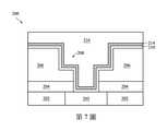
在幾乎所有的金屬材料212的原子與摻質215反應(例如由其鍵結)的實施例中,金屬材料212可以被轉換或轉化為摻雜的襯墊結構214,如第6圖所示。當未形成可選的阻障層210時,摻雜的襯墊結構214可以內襯凹槽208的側壁和底部並在介電層206上方。具體而言,摻雜的襯墊結構214可以直接接觸蝕刻停止層204和介電層206的一或多個內表面/邊界。舉例來說,摻雜的襯墊結構214可以直接接觸介電層206的內側壁206S1和內側壁206S2、介電層206的中間邊界206I和蝕刻停止層204的內側壁204S。此外,摻雜的襯墊結構214也可以直接接觸介電層206的頂邊界206T。In embodiments in which substantially all of the atoms of the
在金屬材料212包含Co的範例中,摻雜的襯墊結構214可以包含氮化鈷(例如CoNx、CoN、Co3N、Co4N)、氫化鈷(例如CoHx、CoH、CoH2、CoH3)、碳化鈷(例如CoCx、CoC、Co2C、Co3C)等,取決於在電漿製程213中使用的氣體或前驅物種類。在金屬材料212包含Ru的範例中,摻雜的襯墊結構214可以包含氮化釕(例如RuNx、Ru4N、Ru3N、Ru2N、RuN、RuN2)、碳化釕(例如RuCx、RuC)、Ru-CN、氫化釕複合物等,取決於在電漿製程213中使用的氣體或前驅物種類。在金屬材料212包含Ta的範例中,摻雜的襯墊結構214可以包含氮化鉭(例如TaNx、TaN、Ta2N、Ta3N5、Ta4N5、Ta5N6)、碳化鉭(例如TaCx、TaC、Ta4C3、Ta2C)、氫化鉭(TaHx、TaH2、TaH3)等,取決於在電漿製程213中使用的氣體或前驅物種類。In examples where the
雖然在第6圖(和後圖)中將摻雜的襯墊結構214繪示為單層,但應理解的是,摻雜的襯墊結構214可以形成為多層堆疊,同時仍在本發明實施例的範圍內。舉例來說,摻雜的襯墊結構214可以包含多個層,其中的第一層包含類似於金屬材料212的金屬材料,而沒有或具有大致有限數量的摻質215(例如Co),其中的第二層包類似於金屬材料212的金屬材料,並與一定量的摻質215(例如CoNx)反應。Although the doped
參照第1圖和第7圖,方法100進行至步驟110,其中在摻雜的襯墊結構214上方形成第二金屬材料216以填充凹槽208。在一些實施例中,第二金屬材料216形成為介電層206中的互連結構。在一些實施例中,第二金屬材料216的沉積藉由電化學鍍(electro-chemical plating,ECP)製程、物理氣相沉積(PVD)、化學氣相沉積(CVD)、電漿輔助化學氣相沉積(PECVD)、低壓化學氣相沉積(LPCVD)、原子層沉積(ALD)或其他眾所周知的沉積技術。在一些實施例中,第二金屬材料216至少包含例如銅的主要金屬元素。在一些實施例中,第二金屬材料216還包含添加金屬元素。在一些實施例中,第二金屬材料216中的添加金屬元素是鉭(Ta)、銦(In)、錫(Sn)、鋅(Zn)、錳(Mn)、鉻(Cr)、鈦(Ti)、鍺(Ge)、鍶(Sr)、鉑(Pt)、鎂(Mg)、鋁(Al)或鋯(Zr)。Referring to FIGS. 1 and 7 , the
參照第1圖和第8圖,方法100進行至步驟112,其中移除介電層206上方之第二金屬材料216的一部分。在一些實施例中,移除製程是進行化學機械研磨製程以移除凹槽208外部的可選的阻障層210、摻雜的襯墊結構214和第二金屬材料216的多餘部分,進而暴露出介電層206的頂邊界206T並實現平坦化的表面。1 and 8, the
參照第1圖和第9圖,方法100進行至步驟114,其中可選地對半導體裝置200進行熱處理217。在一些實施例中,熱處理217包含退火製程。在一實施例中,熱處理217在約137°C至約600°C的溫度範圍進行。在另一實施例中,熱處理217在約280°C至約400°C的溫度範圍進行。在一實施例中,熱處理217以約10分鐘至約600分鐘的持續時間進行。在一些實施例中,使用爐、快速熱處理(rapid thermal processing,RTP)或熱板裝置進行熱處理217。可以在進行電漿製程213(第5圖)之後藉由任何熱處理來提供熱處理217。在各種替代實施例中,緊接在電漿製程213之後、緊接在化學機械研磨以移除凹槽208外部的第二金屬材料216的多餘部分之後、或者緊接在頂金屬層上形成鈍化層之後提供熱處理217。Referring to FIGS. 1 and 9 , the
應注意的是,可以反覆進行方法100以形成半導體裝置200的一或多個後續金屬化層。舉例來說,藉由重複步驟102~114,半導體裝置200可以包含另一蝕刻停止層220、另一介電層222、另一可選的阻障層224、另一摻雜的襯墊結構226和另一金屬材料228,如第10圖所示。蝕刻停止層220、介電層222、可選的阻障層224、摻雜的襯墊結構226和金屬材料228大致類似於蝕刻停止層204、介電層206、阻障層210、摻雜的襯墊結構214和金屬材料216。因此,將不重複討論。It should be noted that
在一些實施例中,導電部件203可以設置(或嵌入)在第一金屬化層(例如在第10圖中表示為M0)中,並且形成為另一導電部件的金屬材料228可以設置(或嵌入)在第二金屬化層(例如在第10圖中表示為M2)中。如此一來,第二金屬材料216可以設置(或嵌入)在第一金屬化層和第二金屬化層之間的第三金屬化層(例如在第10圖中表示為M1)中。在一些實施例中,至少部分地由摻雜的襯墊結構214和226包覆的第二金屬材料216被配置為互連結構,以將導電部件203電連接至導電部件228。因此,第二金屬材料216在此可以被稱為「互連結構216」。當互連結構216填充具有上溝槽部分208U和下通孔部分208L的凹槽208時,互連結構216可以承襲凹槽208的形狀以包含填充上溝槽部分208U的溝槽部分和填充下通孔部分208L的導孔部分。在一些實施例中,互連結構216的溝槽部分和導孔部分彼此直接接觸以形成一整塊。In some embodiments,
在一些實施例中,摻雜的襯墊結構214沿著互連結構216的一些邊界延伸,互連結構216嵌在包含介電層206和蝕刻停止層的金屬化層M1中(或未被金屬化層M1暴露出來)。在第10圖的範例中,摻雜的襯墊結構214沿著金屬化層M1中的邊界216A、216B、216C和216D延伸。類似地,在下一個較高的金屬化層M2中的摻雜的襯墊結構226沿著嵌在金屬化層M2中的互連結構228的一些邊界延伸。此外,摻雜的襯墊結構226也可以沿著由金屬化層M1暴露出的互連結構216的邊界延伸。舉例來說,摻雜的襯墊結構226沿著由金屬化層M1暴露出的互連結構216的邊界216E延伸。In some embodiments, doped
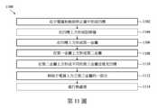
第11圖是根據本發明實施例的各個面向繪示用於製造半導體裝置300的方法1100的流程圖。第12、13、14、15、16、17和18圖根據第11圖的方法1100的實施例繪示在各個製造階段的半導體裝置300的剖面示意圖。半導體裝置300可以包含在微處理器、記憶單元及/或其他積體電路中。應注意的是,第11圖的實施例沒有製造完整的半導體裝置300。可以使用互補式金屬氧化物半導體(CMOS)技術製程來製造完整的半導體裝置300。因此,應理解的是,可以在第11圖的方法1100之前、期間和之後提供額外的製程,並僅在此簡要描述一些其他製程。另外,為了更加理解本發明實施例,簡化第12圖至第18圖。舉例來說,雖然圖式繪示半導體裝置300,但應理解的是,積體電路可以包含許多其他裝置,包含電晶體、電阻器、電容器、電感器、保險絲等。FIG. 11 is a flowchart illustrating various aspects of a
參照第11圖和第12圖,方法1100開始於步驟1102,其中在蝕刻停止層304和介電層(或介電材料)306中形成凹槽308。在一些實施例中,蝕刻停止層304和介電層306可以形成金屬間介電層的一部分。這種金屬間介電層有時被稱為金屬化層,其包含嵌在相應的介電層或材料內的一或多個互連結構。互連結構可以由至少一種金屬材料形成,例如銅(Cu),這將在以下討論。在一些實施例中,蝕刻停止層304形成在半導體基底302上方並在介電層306下方。在一些實施例中,凹槽308形成在介電層306和蝕刻停止層304中,例如至少部分地延伸穿過介電層306和蝕刻停止層304。Referring to FIGS. 11 and 12 ,
半導體基底302是如應用在半導體積體電路製造中的基底,並且可以在其中及/或其上形成積體電路。如本文所用,用語「半導體基底」是指包含半導體材料的任何構造,舉例來說,具有或沒有磊晶層的矽基底、含有埋藏絕緣層的絕緣體上覆矽基底、或具有矽鍺層的基底。如本文所用,用語「積體電路」是指具有多個單獨的電路元件的電子電路,例如電晶體、二極體、電阻器、電容器、電感器以及其他主動和被動半導體裝置。如圖所示,可以在半導體基底302中及/或上(例如在由凹槽308暴露出的半導體基底302中)形成導電區303。導電區303可以是導電路徑的一部分,並且具有可以藉由例如化學機械研磨的平坦化製程處理之暴露表面。用於導電區303的合適材料可以包含但不限於例如銅、鋁、銅合金或其他移動導電材料。含有這種銅導電區303的半導體基底302可以是半導體裝置300的第一或任何後續金屬化層。The
蝕刻停止層304的功能是在後續的蝕刻期間控制終點。在一些實施例中,蝕刻停止層304由氧化矽、氮化矽、碳化矽、氮氧化矽或前述之組合形成。在一些實施例中,蝕刻停止層304的厚度為約10埃至約1000埃。藉由多種技術中的任何一種來形成蝕刻停止層304,包含低壓化學氣相沉積(LPCVD)、常壓化學氣相沉積(APCVD)、電漿輔助化學氣相沉積(PECVD)、物理氣相沉積(PVD)、濺鍍和未來開發的沉積方法。The function of the
介電層306可以是單層或多層結構。在一些實施例中,介電層306的厚度隨所應用的技術而改變,例如厚度為約1000埃至約30000埃。在一些實施例中,介電層306是氧化矽、碳摻雜的氧化矽、介電常數值(k值)小於約4.0的相對低介電常數介電材料或前述之組合。在一些實施例中,介電層306由包含低介電常數介電材料、極低介電常數介電材料、多孔低介電常數介電材料及前述之組合的材料形成。用語「低介電常數」用於定義介電材料的介電常數為3.0或更小。用語「極低介電常數(ELK)」是指介電常數為2.5或更小,並且較佳為1.9至2.5。用語「多孔低介電常數」是指介電材料的介電常數為2.0或更小,並且較佳為1.5或更小。可以根據實施例應用各式各樣的低介電常數材料,例如旋塗式無機介電質、旋塗式有機介電質、多孔介電材料、有機聚合物、有機矽玻璃、FSG(SiOF系列材料)、HSQ(氫矽倍半氧烷)系列材料、MSQ(甲基矽倍半氧烷)系列材料或多孔有機系列材料。在一些實施例中,藉由多種技術中的任何一種來沉積介電層306,例如化學氣相沉積(CVD)、物理氣相沉積(PVD)、原子層沉積(ALD)、遠距電漿輔助化學氣相沉積(RPECVD)、液態霧化源化學沉積(LSMCD)、塗覆、旋塗或其他適於在基板上方形成薄膜層的製程。
在實施例中,介電層306是含氮層、含碳層或含碳且含氮層,用於在隨後的化學機械研磨製程期間提升耐腐蝕性及/或增加電遷移電阻。在一實施例中,介電層306是含矽且含氮的介電層。在另一實施例中,介電層306是含矽和含碳的介電層。在又一實施例中,介電層306是含矽、含氮且含碳的介電層。在一實施例中,介電層306具有的碳對矽的重量比等於或大於約0.5。在另一實施例中,介電層306具有的氮對矽的重量比等於或大於約0.3。在又一實施例中,介電層306具有的碳對矽的重量比等於或大於約0.5,並且氮對矽的重量比等於或大於約0.3。In an embodiment, the
凹槽308是例示性雙鑲嵌開口,其包含上溝槽部分308U和下通孔部分308L。在介電層306和蝕刻停止層304中圖案化凹槽308以界定半導體基底302上的接觸區。雖然實施例繪示金屬間介電層中的雙鑲嵌開口,但也需要在金屬間介電層中使用單個金屬鑲嵌開口。在包含「導孔先製」圖案化方法或「溝槽先製」圖案化方法的雙鑲嵌技術中,上溝槽部分308U和下通孔部分308L的形成可以使用具有遮罩技術和非等向性蝕刻操作(例如電漿蝕刻或反應離子蝕刻)的典型微影。在替代實施例中,在介電層306上或中間沉積底部蝕刻停止層(未繪示)、中間蝕刻停止層(未繪示)、研磨停止層(未繪示)或抗反射塗(ARC)層提供何時結束特定蝕刻製程的清楚指示。
參照第11圖和第13圖,方法1100進行至步驟1104,其中在上述結構上形成阻障層310,以內襯凹槽308的側壁和底部並在介電層306上方。在一些實施例中,阻障層310可以是可選的。阻障層310可以作為阻障層以防止隨後形成的導體擴散到下方的介電層306中。在一些實施例中,阻障層310包含金屬材料,例如鉭(Ta)、鈦(Ti)、鎢(W)和鈦(Ti)。在一些實施例中,阻障層310包含上述金屬材料的化合物或合金,例如氮化鉭(TaN)、氮化鉭矽(TaNSi)、鈦鎢(TiW)和氮化鈦矽(TiNSi)。在一些實施例中,阻障層310的厚度為約10埃至約250埃。Referring to FIGS. 11 and 13 ,
參照第11圖和第14圖,方法1100進行至步驟1106,其中在上述結構上形成第一金屬材料312,以內襯凹槽308的側壁和底部並在阻障層310(如果形成)上方。當未形成可選的阻障層310時,第一金屬材料312可以直接接觸凹槽308的側壁和底部並在介電層306上方。第一金屬材料312包含選自以下群組的至少一種材料:鈷(Co)、釕(Ru)、鉭(Ta)、鈦(Ti)、鎢(W)、鉬(Mo)、鋅(Zn)、鋁(Al)和錳(Mn)。在一些實施例中,第一金屬材料312的厚度為約1埃至約80埃。在一些實施例中,第一金屬材料312的厚度在約2.5埃至約25埃的範圍。在一些實施例中,第一金屬材料312的沉積藉由使用物理氣相沉積(PVD)、化學氣相沉積(CVD)、電漿輔助化學氣相沉積(PECVD)、低壓化學氣相沉積(LPCVD)、原子層沉積(ALD)或其他眾所周知的沉積技術。11 and 14, the
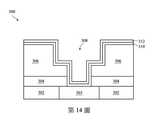
參照第11圖和第15圖,方法1100進行至步驟1108,其中在上述結構上形成第二金屬材料314以內襯凹槽308的側壁和底部並在第一金屬材料312上方。第二金屬材料314包含選自以下群組的至少一種材料:鈷(Co)、釕(Ru)、鉭(Ta)、鈦(Ti)、鎢(W)、鉬(Mo)、鋅(Zn)、鋁(Al)和錳(Mn)。在一些實施例中,第二金屬材料314由不同於第一金屬材料312的材料形成。如此一來,第一金屬材料312和第二金屬材料314可以形成合金襯墊結構,下文稱為合金襯墊結構316。雖然在第15圖(和後圖)中將合金襯墊結構316繪示為兩層的堆疊,但應理解的是,合金襯墊結構316可以形成為任意數量層的堆疊,每一層包含以上列出的金屬材料之一(例如Co、Ru、Ta、Ti、W、Mo、Zn、Al、Mn),同時仍在本發明實施例的範圍內。舉例來說,形成為兩層的堆疊的合金襯墊結構316可以包含選自以下群組的合金:CoRu、CoTa、CoTi、CoMn、CoMo、CoZn、CoAl、CoW、RuTa、RuTi、RuW、RuMo、RuZn、RuAl和RuMn。在一些實施例中,第二金屬材料314的厚度為約1埃至約80埃。在一些實施例中,第二金屬材料314的厚度在約2.5埃至約25埃的範圍。在一些實施例中,第一金屬材料312和第二金屬材料314的總厚度可以在約5埃至約50埃的範圍。在一些實施例中,第二金屬材料314的沉積藉由使用物理氣相沉積(PVD)、化學氣相沉積(CVD)、電漿輔助化學氣相沉積(PECVD)、低壓化學氣相沉積(LPCVD)、原子層沉積(ALD)或其他眾所周知的沉積技術。11 and 15, the
參照第11圖和第16圖,方法1100進行至步驟1110,其中在合金襯墊結構316上方形成第三金屬材料320以填充凹槽308。在一些實施例中,第三金屬材料320形成為介電層306中的互連結構。在一些實施例中,第三金屬材料320的沉積藉由電化學鍍(ECP)製程、物理氣相沉積(PVD)、化學氣相沉積(CVD)、電漿輔助化學氣相沉積(PECVD)、低壓化學氣相沉積(LPCVD)、原子層沉積(ALD)或其他眾所周知的沉積技術。在一些實施例中,第三金屬材料320至少包含例如銅的主要金屬元素。在一些實施例中,第三金屬材料320還包含添加金屬元素。在一些實施例中,第三金屬材料320中的添加金屬元素是鉭(Ta)、銦(In)、錫(Sn)、鋅(Zn)、錳(Mn)、鉻(Cr)、鈦(Ti)、鍺(Ge)、鍶(Sr)、鉑(Pt)、鎂(Mg)、鋁(Al)或鋯(Zr)。Referring to FIGS. 11 and 16 , the
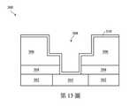
參照第11圖和第17圖,方法100進行至步驟1112,其中移除介電層306上方之第三金屬材料320的一部分。在一些實施例中,移除製程是進行化學機械研磨製程以移除凹槽308外部的可選的阻障層310、合金襯墊結構316和第三金屬材料320的多餘部分,進而暴露出介電層306的頂邊界306T並實現平坦化的表面。Referring to FIGS. 11 and 17, the
參照第11圖和第18圖,方法1100進行至步驟1114,其中可選地對半導體裝置300進行熱處理321。在一些實施例中,熱處理321包含退火製程。在一實施例中,熱處理321在約137°C至約600°C的溫度範圍進行。在另一實施例中,熱處理321在約280°C至約400°C的溫度範圍進行。在一實施例中,熱處理321以約10分鐘至約600分鐘的持續時間進行。在一些實施例中,使用爐、快速熱處理(RTP)或熱板裝置進行熱處理321。在各種替代實施例中,緊接在形成第二金屬材料314之後、緊接在化學機械研磨以移除凹槽308外部的第二金屬材料314的多餘部分之後、或者緊接在頂金屬層上形成鈍化層之後提供熱處理321。Referring to FIGS. 11 and 18 , the
類似於方法100,應注意的是,可以反覆進行方法1100以形成半導體裝置300的一或多個後續金屬化層。如此一來,第三金屬材料320可以設置(或嵌入)在下金屬化層(例如形成有導電區303的金屬化層,在第18圖中表示為M0)和上金屬化層(未繪示)之間的金屬化層(在第18圖中表示為M1)中。在一些實施例中,至少部分地由M1中的合金襯墊結構316和在下一個上金屬化層(例如M2)中的另一合金襯墊結構包覆的第三金屬材料320被配置為互連結構,以將導電部件303電連接至設置(或嵌入)在上金屬化層中的另一導電部件。如此一來,第三金屬材料320在此被稱為「互連結構320」。當互連結構320填充具有上溝槽部分308U和下通孔部分308L的凹槽308時,互連結構320可以承襲凹槽308的形狀以包含填充上溝槽部分308U的溝槽部分和填充下通孔部分308L的導孔部分。在一些實施例中,互連結構320的溝槽部分和導孔部分彼此直接接觸以形成一整塊。Similar to
在一些實施例中,合金襯墊結構316沿著互連結構320的一些邊界延伸,互連結構320嵌在包含介電層306和蝕刻停止層的金屬化層M1中(或未被金屬化層M1暴露出來)。在第18圖的範例中,合金襯墊結構316沿著金屬化層M1中的邊界320A、320B、320C和320D延伸。雖然未繪示,但應理解的是,嵌在下一個較高的金屬化層(例如M2)中的另一合金襯墊結構可以沿著互連結構320的邊界320E延伸。In some embodiments,
以上概述數個實施例之部件,使得本技術領域中具有通常知識者可以更加理解本發明實施例的面向。本技術領域中具有通常知識者應該理解,他們能輕易地以本發明實施例為基礎,設計或修改其他製程和結構,以達到與本文介紹的實施例之相同目的及/或優點。本技術領域中具有通常知識者也應理解,此類等效的結構並未悖離本發明實施例的精神與範圍,並且他們能在不違背本發明實施例的精神和範圍下,做各式各樣的改變、取代和調整。The components of several embodiments are outlined above so that those skilled in the art can better understand aspects of the embodiments of the present invention. Those skilled in the art should appreciate that they can easily use the embodiments of the present invention as a basis to design or modify other processes and structures to achieve the same objectives and/or advantages of the embodiments described herein. Those skilled in the art should also understand that such equivalent structures do not depart from the spirit and scope of the embodiments of the present invention, and they can be made in various forms without departing from the spirit and scope of the embodiments of the present invention. Various changes, substitutions and adjustments.
在一實施例中,半導體裝置包含嵌在第一金屬化層中的互連結構,第一金屬化層包含介電材料。互連結構包含第一金屬材料。半導體裝置包含嵌在第一金屬化層中的第一襯墊結構。第一襯墊結構沿著第一金屬化層中的互連結構的一或多個邊界延伸。第一襯墊結構包含與一或多種摻質反應的第二金屬材料,第二金屬材料不同於第一金屬材料。In one embodiment, the semiconductor device includes an interconnect structure embedded in a first metallization layer, the first metallization layer including a dielectric material. The interconnect structure includes a first metal material. The semiconductor device includes a first pad structure embedded in the first metallization layer. The first pad structure extends along one or more boundaries of the interconnect structure in the first metallization layer. The first pad structure includes a second metal material that is different from the first metal material and reacts with one or more dopants.
在一實施例中,第二金屬材料包含選自以下群組的至少一種材料:鈷(Co)、釕(Ru)、鉭(Ta)、鈦(Ti)、鎢(W)、鉬(Mo)、鋅(Zn)、鋁(Al)和錳(Mn)。In one embodiment, the second metal material includes at least one material selected from the group consisting of cobalt (Co), ruthenium (Ru), tantalum (Ta), titanium (Ti), tungsten (W), molybdenum (Mo) , Zinc (Zn), Aluminum (Al) and Manganese (Mn).
在一實施例中,一或多種摻質各自包含選自以下群組的至少一種:氫原子、氫氧化物原子、氮原子、氫離子、氫氧根離子、氮離子、碳氫離子、氫自由基、氫氧根自由基、氮自由基和碳氫自由基。In one embodiment, the one or more dopants each comprise at least one selected from the group consisting of hydrogen atoms, hydroxide atoms, nitrogen atoms, hydrogen ions, hydroxide ions, nitrogen ions, hydrocarbon ions, hydrogen free radicals, hydroxide radicals, nitrogen radicals and hydrocarbon radicals.
在一實施例中,第一金屬材料包含銅(Cu)。In one embodiment, the first metal material includes copper (Cu).
在一實施例中,半導體裝置更包含:設置在第一金屬化層的介電材料和第一襯墊結構之間的阻障層,其中阻障層包含第三金屬材料的氮化物。In one embodiment, the semiconductor device further includes: a barrier layer disposed between the dielectric material of the first metallization layer and the first liner structure, wherein the barrier layer includes a nitride of the third metal material.
在一實施例中,互連結構包含導孔部分和直接接觸導孔部分的溝槽部分。In one embodiment, the interconnect structure includes a via portion and a trench portion that directly contacts the via portion.
在一實施例中,半導體裝置更包含:嵌在第一金屬化層上方之第二金屬化層中的第二襯墊結構,其中第二襯墊結構包含與一或多種摻質反應的第二金屬材料。In one embodiment, the semiconductor device further includes: a second liner structure embedded in a second metallization layer over the first metallization layer, wherein the second liner structure includes a second liner reactive with one or more dopants metallic material.
在一實施例中,互連結構被第一襯墊結構和第二襯墊結構包覆。In one embodiment, the interconnect structure is encapsulated by the first pad structure and the second pad structure.
在一實施例中,藉由電漿製程形成與第一襯墊結構的一或多種摻質反應的第二金屬材料。In one embodiment, the second metal material that reacts with one or more dopants of the first pad structure is formed by a plasma process.
在一實施例中,電漿製程包含選自以下群組的至少一種電漿製程:氫電漿製程、氮電漿製程、氨電漿製程和甲醇電漿製程。In one embodiment, the plasma process includes at least one plasma process selected from the group consisting of a hydrogen plasma process, a nitrogen plasma process, an ammonia plasma process, and a methanol plasma process.
在另一實施例中,半導體裝置包含嵌在第一金屬化層中的互連結構,第一金屬化層包含介電材料。互連結構包含第一金屬材料。半導體裝置包含嵌在第一金屬化層中的第一襯墊結構。第一襯墊結構沿著第一金屬化層中的互連結構的一或多個邊界延伸。第一襯墊結構包含與第一金屬材料不同的多個第二金屬材料中的至少第一個和第二個的合金。In another embodiment, a semiconductor device includes an interconnect structure embedded in a first metallization layer, the first metallization layer including a dielectric material. The interconnect structure includes a first metal material. The semiconductor device includes a first pad structure embedded in the first metallization layer. The first pad structure extends along one or more boundaries of the interconnect structure in the first metallization layer. The first pad structure includes an alloy of at least a first and a second of a plurality of second metallic materials different from the first metallic material.
在一實施例中,多個第二金屬材料包含鈷(Co)、釕(Ru)、鉭(Ta)、鈦(Ti)、鎢(W)、鉬(Mo)、鋅(Zn)、鋁(Al)和錳(Mn)。In one embodiment, the plurality of second metal materials include cobalt (Co), ruthenium (Ru), tantalum (Ta), titanium (Ti), tungsten (W), molybdenum (Mo), zinc (Zn), aluminum ( Al) and manganese (Mn).
在一實施例中,第一金屬材料包含銅(Cu)。In one embodiment, the first metal material includes copper (Cu).
在一實施例中,半導體裝置更包含:設置在第一金屬化層的介電材料和第一襯墊結構之間的阻障層,其中阻障層包含第三金屬材料的氮化物。In one embodiment, the semiconductor device further includes: a barrier layer disposed between the dielectric material of the first metallization layer and the first liner structure, wherein the barrier layer includes a nitride of the third metal material.
在一實施例中,互連結構包含導孔部分和直接接觸導孔部分的溝槽部分。In one embodiment, the interconnect structure includes a via portion and a trench portion that directly contacts the via portion.
在一實施例中,半導體裝置更包含嵌在第一金屬化層上方之第二金屬化層中的第二襯墊結構,其中第二襯墊結構包含多個第二金屬材料中的第一個和第二個的合金。In one embodiment, the semiconductor device further includes a second pad structure embedded in a second metallization layer over the first metallization layer, wherein the second pad structure includes a first of the plurality of second metal materials and the second alloy.
在一實施例中,互連結構被第一襯墊結構和第二襯墊結構包覆。In one embodiment, the interconnect structure is encapsulated by the first pad structure and the second pad structure.
在又一實施例中,半導體裝置的形成方法包含形成至少部分地延伸穿過介電層的空腔。此方法包含形成沿著空腔延伸的襯墊結構。襯墊結構包含藉由電漿製程鈍化的第一金屬材料或第二金屬材料和第三金屬材料的合金。此方法包含用第四金屬材料填充空腔以形成互連結構。第四金屬材料不同於第一金屬材料、第二金屬材料和第三金屬材料中的每一個。In yet another embodiment, a method of forming a semiconductor device includes forming a cavity extending at least partially through a dielectric layer. The method includes forming a liner structure extending along the cavity. The pad structure includes a first metal material or an alloy of a second metal material and a third metal material passivated by a plasma process. The method includes filling the cavity with a fourth metal material to form an interconnect structure. The fourth metallic material is different from each of the first metallic material, the second metallic material, and the third metallic material.
在一實施例中,第一金屬材料包含選自以下群組的至少一種材料:鈷(Co)、釕(Ru)、鉭(Ta)、鈦(Ti)、鎢(W)、鉬(Mo)、鋅(Zn)、鋁(Al)和錳(Mn);電漿製程包含選自以下群組的至少一種電漿製程:氫電漿製程、氮電漿製程、氨電漿製程和甲醇電漿製程;以及第四金屬材料包含銅(Cu)。In one embodiment, the first metal material includes at least one material selected from the group consisting of cobalt (Co), ruthenium (Ru), tantalum (Ta), titanium (Ti), tungsten (W), molybdenum (Mo) , zinc (Zn), aluminum (Al), and manganese (Mn); the plasma process includes at least one plasma process selected from the group consisting of hydrogen plasma process, nitrogen plasma process, ammonia plasma process, and methanol plasma process process; and the fourth metal material includes copper (Cu).
在一實施例中,第二金屬材料和第三金屬材料各自包含選自以下群組的至少一種材料:鈷(Co)、釕(Ru)、鉭(Ta)、鈦(Ti)、鎢(W)、鉬(Mo)、鋅(Zn)、鋁(Al)和錳(Mn);以及第四金屬材料包含銅(Cu)。In one embodiment, the second metal material and the third metal material each include at least one material selected from the group consisting of cobalt (Co), ruthenium (Ru), tantalum (Ta), titanium (Ti), tungsten (W ), molybdenum (Mo), zinc (Zn), aluminum (Al), and manganese (Mn); and the fourth metal material includes copper (Cu).
100,1100:方法102,104,106,108,110,112,114,1102,1104,1106,1108,1110,1112,1114:步驟200,300:半導體裝置202,302:半導體基底203,303:導電區204,220,304:蝕刻停止層204S,206S1,206S2:內側壁206,222,306:介電層206I:中間邊界206T,212T,306T:頂邊界208,308:凹槽208L,308L:下通孔部分208U,308U:上溝槽部分210,224,310:阻障層212,312:第一金屬材料213:處理製程214,226:摻雜的襯墊結構215:摻質216,314:第二金屬材料216A,216B,216C,216D,216E,320A,320B,320C,320D,320E:邊界217,321:熱處理228:金屬材料316:合金襯墊結構320:第三金屬材料M0,M1,M2:金屬化層100, 1100:
藉由以下的詳細描述配合所附圖式,可以更加理解本發明實施例的內容。需強調的是,根據產業上的標準慣例,許多部件並未按照比例繪製。事實上,為了能清楚地討論,各種部件的尺寸可能被任意地增加或減少。第1圖根據一些實施例繪示用於形成半導體裝置的例示性方法的流程圖。第2、3、4、5、6、7、8、9和10圖根據一些實施例繪示在藉由第1圖的方法製造之各個製造階段期間的例示性半導體裝置的剖面圖。第11圖根據一些實施例繪示用於形成半導體裝置的例示性方法的流程圖。第12、13、14、15、16、17和18圖根據一些實施例繪示在藉由第11圖的方法製造之各個製造階段期間的例示性半導體裝置的剖面圖。The content of the embodiments of the present invention can be better understood through the following detailed description in conjunction with the accompanying drawings. It is emphasized that, in accordance with standard industry practice, many components are not drawn to scale. In fact, the dimensions of the various components may be arbitrarily increased or decreased for clarity of discussion.FIG. 1 depicts a flowchart of an exemplary method for forming a semiconductor device in accordance with some embodiments.FIGS. 2, 3, 4, 5, 6, 7, 8, 9, and 10 depict cross-sectional views of exemplary semiconductor devices during various fabrication stages fabricated by the method of FIG. 1, according to some embodiments.11 depicts a flowchart of an exemplary method for forming a semiconductor device, according to some embodiments.FIGS. 12, 13, 14, 15, 16, 17, and 18 depict cross-sectional views of exemplary semiconductor devices during various fabrication stages fabricated by the method of FIG. 11, according to some embodiments.
200:半導體裝置200: Semiconductor Devices
202:半導體基底202: Semiconductor substrates
203:導電區203: Conductive area
204,220:蝕刻停止層204,220: Etch Stop Layer
206,222:介電層206,222: Dielectric Layer
208:凹槽208: Groove
208L:下通孔部分208L: Lower through hole part
208U:上溝槽部分208U: Upper groove part
210,224:阻障層210, 224: Barrier Layer
214,226:摻雜的襯墊結構214, 226: Doped Pad Structure
216:第二金屬材料216: Second Metal Material
216A,216B,216C,216D,216E:邊界216A, 216B, 216C, 216D, 216E: Boundaries
228:金屬材料228: Metal Materials
M0,M1,M2:金屬化層M0, M1, M2: metallization layer
Claims (1)
Translated fromChineseApplications Claiming Priority (2)
| Application Number | Priority Date | Filing Date | Title |
|---|---|---|---|
| US16/912,284 | 2020-06-25 | ||
| US16/912,284US12027419B2 (en) | 2020-06-25 | 2020-06-25 | Semiconductor device including liner structure |
Publications (1)
| Publication Number | Publication Date |
|---|---|
| TW202201786Atrue TW202201786A (en) | 2022-01-01 |
Family
ID=78162138
Family Applications (1)
| Application Number | Title | Priority Date | Filing Date |
|---|---|---|---|
| TW110122533ATW202201786A (en) | 2020-06-25 | 2021-06-21 | Semiconductor device |
Country Status (3)
| Country | Link |
|---|---|
| US (2) | US12027419B2 (en) |
| CN (1) | CN113571493A (en) |
| TW (1) | TW202201786A (en) |
Families Citing this family (3)
| Publication number | Priority date | Publication date | Assignee | Title |
|---|---|---|---|---|
| US12027419B2 (en)* | 2020-06-25 | 2024-07-02 | Taiwan Semiconductor Manufacturing Company Limited | Semiconductor device including liner structure |
| JP2023031707A (en)* | 2021-08-25 | 2023-03-09 | キオクシア株式会社 | Semiconductor device and method for manufacturing the same |
| WO2025038179A1 (en)* | 2023-08-14 | 2025-02-20 | Applied Materials, Inc. | Metal implantation to barrier or liner for interconnect |
Family Cites Families (34)
| Publication number | Priority date | Publication date | Assignee | Title |
|---|---|---|---|---|
| TW310461B (en)* | 1995-11-10 | 1997-07-11 | Matsushita Electric Industrial Co Ltd | |
| KR100269878B1 (en)* | 1997-08-22 | 2000-12-01 | 윤종용 | Method for forming metal interconnection of semiconductor device |
| US7253109B2 (en)* | 1997-11-26 | 2007-08-07 | Applied Materials, Inc. | Method of depositing a tantalum nitride/tantalum diffusion barrier layer system |
| US6627995B2 (en)* | 2000-03-03 | 2003-09-30 | Cvc Products, Inc. | Microelectronic interconnect material with adhesion promotion layer and fabrication method |
| US9051641B2 (en)* | 2001-07-25 | 2015-06-09 | Applied Materials, Inc. | Cobalt deposition on barrier surfaces |
| KR100805843B1 (en)* | 2001-12-28 | 2008-02-21 | 에이에스엠지니텍코리아 주식회사 | Copper wiring forming method, semiconductor device and copper wiring forming system manufactured accordingly |
| US7211508B2 (en)* | 2003-06-18 | 2007-05-01 | Applied Materials, Inc. | Atomic layer deposition of tantalum based barrier materials |
| US20060252252A1 (en)* | 2005-03-18 | 2006-11-09 | Zhize Zhu | Electroless deposition processes and compositions for forming interconnects |
| KR100707656B1 (en)* | 2005-10-10 | 2007-04-13 | 동부일렉트로닉스 주식회사 | A method of forming a metal wiring and a semiconductor device comprising the metal wiring formed thereby |
| US8026605B2 (en)* | 2006-12-14 | 2011-09-27 | Lam Research Corporation | Interconnect structure and method of manufacturing a damascene structure |
| US20080242088A1 (en)* | 2007-03-29 | 2008-10-02 | Tokyo Electron Limited | Method of forming low resistivity copper film structures |
| US7704879B2 (en)* | 2007-09-27 | 2010-04-27 | Tokyo Electron Limited | Method of forming low-resistivity recessed features in copper metallization |
| KR20090053991A (en)* | 2007-11-26 | 2009-05-29 | 주식회사 동부하이텍 | Manufacturing method of semiconductor device |
| US7655564B2 (en)* | 2007-12-12 | 2010-02-02 | Asm Japan, K.K. | Method for forming Ta-Ru liner layer for Cu wiring |
| US8703605B2 (en)* | 2007-12-18 | 2014-04-22 | Byung Chun Yang | High yield and high throughput method for the manufacture of integrated circuit devices of improved integrity, performance and reliability |
| US8679970B2 (en)* | 2008-05-21 | 2014-03-25 | International Business Machines Corporation | Structure and process for conductive contact integration |
| US8524600B2 (en)* | 2011-03-31 | 2013-09-03 | Applied Materials, Inc. | Post deposition treatments for CVD cobalt films |
| TWI645511B (en)* | 2011-12-01 | 2018-12-21 | 美商應用材料股份有限公司 | Doped tantalum nitride for copper barrier applications |
| US9048294B2 (en)* | 2012-04-13 | 2015-06-02 | Applied Materials, Inc. | Methods for depositing manganese and manganese nitrides |
| US8722531B1 (en)* | 2012-11-01 | 2014-05-13 | Taiwan Semiconductor Manufacturing Company, Ltd. | Barrier layer for copper interconnect |
| US9966339B2 (en)* | 2014-03-14 | 2018-05-08 | Taiwan Semiconductor Manufacturing Company | Barrier structure for copper interconnect |
| US20150357236A1 (en)* | 2014-06-08 | 2015-12-10 | International Business Machines Corporation | Ultrathin Multilayer Metal Alloy Liner for Nano Cu Interconnects |
| US9406554B2 (en)* | 2014-09-30 | 2016-08-02 | International Business Machines Corporation | Diffusion barrier layer formation |
| KR20160112203A (en)* | 2015-03-18 | 2016-09-28 | 삼성전자주식회사 | Wiring structures, methods of forming wiring structures and methods of manufacturing semiconductor devices |
| US10090195B2 (en)* | 2015-10-21 | 2018-10-02 | Globalfoundries Inc. | Method including a formation of a diffusion barrier and semiconductor structure including a diffusion barrier |
| US9406617B1 (en)* | 2015-11-19 | 2016-08-02 | International Business Machines Corporation | Structure and process for W contacts |
| US9805976B2 (en)* | 2016-01-08 | 2017-10-31 | Applied Materials, Inc. | Co or Ni and Cu integration for small and large features in integrated circuits |
| US10157784B2 (en)* | 2016-02-12 | 2018-12-18 | Tokyo Electron Limited | Integration of a self-forming barrier layer and a ruthenium metal liner in copper metallization |
| TWI746851B (en)* | 2018-05-21 | 2021-11-21 | 聯華電子股份有限公司 | Metal interconnect structure and method for fabricating the same |
| US10916503B2 (en)* | 2018-09-11 | 2021-02-09 | International Business Machines Corporation | Back end of line metallization structure |
| US11152258B2 (en)* | 2019-09-17 | 2021-10-19 | Taiwan Semiconductor Manufacturing Company, Ltd. | Method of forming an interconnect in a semiconductor device |
| US11854878B2 (en)* | 2019-12-27 | 2023-12-26 | Taiwan Semiconductor Manufacturing Ltd. | Bi-layer alloy liner for interconnect metallization and methods of forming the same |
| US11270911B2 (en)* | 2020-05-06 | 2022-03-08 | Applied Materials Inc. | Doping of metal barrier layers |
| US12027419B2 (en)* | 2020-06-25 | 2024-07-02 | Taiwan Semiconductor Manufacturing Company Limited | Semiconductor device including liner structure |
- 2020
- 2020-06-25USUS16/912,284patent/US12027419B2/enactiveActive
- 2021
- 2021-06-17CNCN202110671401.XApatent/CN113571493A/enactivePending
- 2021-06-21TWTW110122533Apatent/TW202201786A/enunknown
- 2024
- 2024-06-04USUS18/733,512patent/US20240321632A1/enactivePending
Also Published As
| Publication number | Publication date |
|---|---|
| US12027419B2 (en) | 2024-07-02 |
| CN113571493A (en) | 2021-10-29 |
| US20210407852A1 (en) | 2021-12-30 |
| US20240321632A1 (en) | 2024-09-26 |
Similar Documents
| Publication | Publication Date | Title |
|---|---|---|
| US7524755B2 (en) | Entire encapsulation of Cu interconnects using self-aligned CuSiN film | |
| US8361900B2 (en) | Barrier layer for copper interconnect | |
| US7154178B2 (en) | Multilayer diffusion barrier for copper interconnections | |
| US7898082B2 (en) | Nitrogen rich barrier layers and methods of fabrication thereof | |
| US9064934B2 (en) | Barrier layer for copper interconnect | |
| US9966339B2 (en) | Barrier structure for copper interconnect | |
| US6686662B2 (en) | Semiconductor device barrier layer | |
| US9984975B2 (en) | Barrier structure for copper interconnect | |
| US20080280432A1 (en) | Barrier Material and Process for Cu Interconnect | |
| US11164776B2 (en) | Metallic interconnect structure | |
| US20110101529A1 (en) | Barrier layer for copper interconnect | |
| US20100252930A1 (en) | Method for Improving Performance of Etch Stop Layer | |
| US20240321632A1 (en) | Semiconductor device including liner structure | |
| US7790617B2 (en) | Formation of metal silicide layer over copper interconnect for reliability enhancement | |
| CN100403512C (en) | Copper-barrier layer inlaid internal connection structure with low resistance value and its making method | |
| US7223692B2 (en) | Multi-level semiconductor device with capping layer for improved adhesion | |
| US20050277292A1 (en) | Method for fabricating low resistivity barrier for copper interconnect | |
| US9893144B1 (en) | Methods for fabricating metal-insulator-metal capacitors | |
| TW202111870A (en) | Methods and apparatus for hybrid feature metallization | |
| KR100914982B1 (en) | Metal wiring of semiconductor device and method of manufacturing the same | |
| US20040082169A1 (en) | Deposition of barrier metal in damascene interconnects using metal carbonyl | |
| JP5217272B2 (en) | Wiring forming method and semiconductor device manufacturing method | |
| US20250079313A1 (en) | Semiconductor structure and manufacturing method thereof | |
| CN109216261B (en) | Semiconductor structure and forming method thereof | |
| TW202431541A (en) | Plasma treatment of barrier and liner layers |