TW202201087A - Liquid crystal display device - Google Patents
Liquid crystal display deviceDownload PDFInfo
- Publication number
- TW202201087A TW202201087ATW110132501ATW110132501ATW202201087ATW 202201087 ATW202201087 ATW 202201087ATW 110132501 ATW110132501 ATW 110132501ATW 110132501 ATW110132501 ATW 110132501ATW 202201087 ATW202201087 ATW 202201087A
- Authority
- TW
- Taiwan
- Prior art keywords
- wiring
- transistor
- terminal
- electrically connected
- flip
- Prior art date
Links
Images


Classifications
- G—PHYSICS
- G09—EDUCATION; CRYPTOGRAPHY; DISPLAY; ADVERTISING; SEALS
- G09G—ARRANGEMENTS OR CIRCUITS FOR CONTROL OF INDICATING DEVICES USING STATIC MEANS TO PRESENT VARIABLE INFORMATION
- G09G3/00—Control arrangements or circuits, of interest only in connection with visual indicators other than cathode-ray tubes
- G09G3/20—Control arrangements or circuits, of interest only in connection with visual indicators other than cathode-ray tubes for presentation of an assembly of a number of characters, e.g. a page, by composing the assembly by combination of individual elements arranged in a matrix no fixed position being assigned to or needed to be assigned to the individual characters or partial characters
- G09G3/34—Control arrangements or circuits, of interest only in connection with visual indicators other than cathode-ray tubes for presentation of an assembly of a number of characters, e.g. a page, by composing the assembly by combination of individual elements arranged in a matrix no fixed position being assigned to or needed to be assigned to the individual characters or partial characters by control of light from an independent source
- G09G3/3406—Control of illumination source
- G09G3/342—Control of illumination source using several illumination sources separately controlled corresponding to different display panel areas, e.g. along one dimension such as lines
- G—PHYSICS
- G02—OPTICS
- G02F—OPTICAL DEVICES OR ARRANGEMENTS FOR THE CONTROL OF LIGHT BY MODIFICATION OF THE OPTICAL PROPERTIES OF THE MEDIA OF THE ELEMENTS INVOLVED THEREIN; NON-LINEAR OPTICS; FREQUENCY-CHANGING OF LIGHT; OPTICAL LOGIC ELEMENTS; OPTICAL ANALOGUE/DIGITAL CONVERTERS
- G02F1/00—Devices or arrangements for the control of the intensity, colour, phase, polarisation or direction of light arriving from an independent light source, e.g. switching, gating or modulating; Non-linear optics
- G02F1/01—Devices or arrangements for the control of the intensity, colour, phase, polarisation or direction of light arriving from an independent light source, e.g. switching, gating or modulating; Non-linear optics for the control of the intensity, phase, polarisation or colour
- G02F1/13—Devices or arrangements for the control of the intensity, colour, phase, polarisation or direction of light arriving from an independent light source, e.g. switching, gating or modulating; Non-linear optics for the control of the intensity, phase, polarisation or colour based on liquid crystals, e.g. single liquid crystal display cells
- G02F1/133—Constructional arrangements; Operation of liquid crystal cells; Circuit arrangements
- G02F1/13306—Circuit arrangements or driving methods for the control of single liquid crystal cells
- G—PHYSICS
- G02—OPTICS
- G02F—OPTICAL DEVICES OR ARRANGEMENTS FOR THE CONTROL OF LIGHT BY MODIFICATION OF THE OPTICAL PROPERTIES OF THE MEDIA OF THE ELEMENTS INVOLVED THEREIN; NON-LINEAR OPTICS; FREQUENCY-CHANGING OF LIGHT; OPTICAL LOGIC ELEMENTS; OPTICAL ANALOGUE/DIGITAL CONVERTERS
- G02F1/00—Devices or arrangements for the control of the intensity, colour, phase, polarisation or direction of light arriving from an independent light source, e.g. switching, gating or modulating; Non-linear optics
- G02F1/01—Devices or arrangements for the control of the intensity, colour, phase, polarisation or direction of light arriving from an independent light source, e.g. switching, gating or modulating; Non-linear optics for the control of the intensity, phase, polarisation or colour
- G02F1/13—Devices or arrangements for the control of the intensity, colour, phase, polarisation or direction of light arriving from an independent light source, e.g. switching, gating or modulating; Non-linear optics for the control of the intensity, phase, polarisation or colour based on liquid crystals, e.g. single liquid crystal display cells
- G02F1/133—Constructional arrangements; Operation of liquid crystal cells; Circuit arrangements
- G02F1/1333—Constructional arrangements; Manufacturing methods
- G02F1/1345—Conductors connecting electrodes to cell terminals
- G02F1/13452—Conductors connecting driver circuitry and terminals of panels
- G—PHYSICS
- G02—OPTICS
- G02F—OPTICAL DEVICES OR ARRANGEMENTS FOR THE CONTROL OF LIGHT BY MODIFICATION OF THE OPTICAL PROPERTIES OF THE MEDIA OF THE ELEMENTS INVOLVED THEREIN; NON-LINEAR OPTICS; FREQUENCY-CHANGING OF LIGHT; OPTICAL LOGIC ELEMENTS; OPTICAL ANALOGUE/DIGITAL CONVERTERS
- G02F1/00—Devices or arrangements for the control of the intensity, colour, phase, polarisation or direction of light arriving from an independent light source, e.g. switching, gating or modulating; Non-linear optics
- G02F1/01—Devices or arrangements for the control of the intensity, colour, phase, polarisation or direction of light arriving from an independent light source, e.g. switching, gating or modulating; Non-linear optics for the control of the intensity, phase, polarisation or colour
- G02F1/13—Devices or arrangements for the control of the intensity, colour, phase, polarisation or direction of light arriving from an independent light source, e.g. switching, gating or modulating; Non-linear optics for the control of the intensity, phase, polarisation or colour based on liquid crystals, e.g. single liquid crystal display cells
- G02F1/133—Constructional arrangements; Operation of liquid crystal cells; Circuit arrangements
- G02F1/136—Liquid crystal cells structurally associated with a semi-conducting layer or substrate, e.g. cells forming part of an integrated circuit
- G02F1/1362—Active matrix addressed cells
- G02F1/136213—Storage capacitors associated with the pixel electrode
- G—PHYSICS
- G02—OPTICS
- G02F—OPTICAL DEVICES OR ARRANGEMENTS FOR THE CONTROL OF LIGHT BY MODIFICATION OF THE OPTICAL PROPERTIES OF THE MEDIA OF THE ELEMENTS INVOLVED THEREIN; NON-LINEAR OPTICS; FREQUENCY-CHANGING OF LIGHT; OPTICAL LOGIC ELEMENTS; OPTICAL ANALOGUE/DIGITAL CONVERTERS
- G02F1/00—Devices or arrangements for the control of the intensity, colour, phase, polarisation or direction of light arriving from an independent light source, e.g. switching, gating or modulating; Non-linear optics
- G02F1/01—Devices or arrangements for the control of the intensity, colour, phase, polarisation or direction of light arriving from an independent light source, e.g. switching, gating or modulating; Non-linear optics for the control of the intensity, phase, polarisation or colour
- G02F1/13—Devices or arrangements for the control of the intensity, colour, phase, polarisation or direction of light arriving from an independent light source, e.g. switching, gating or modulating; Non-linear optics for the control of the intensity, phase, polarisation or colour based on liquid crystals, e.g. single liquid crystal display cells
- G02F1/133—Constructional arrangements; Operation of liquid crystal cells; Circuit arrangements
- G02F1/136—Liquid crystal cells structurally associated with a semi-conducting layer or substrate, e.g. cells forming part of an integrated circuit
- G02F1/1362—Active matrix addressed cells
- G02F1/136286—Wiring, e.g. gate line, drain line
- G—PHYSICS
- G02—OPTICS
- G02F—OPTICAL DEVICES OR ARRANGEMENTS FOR THE CONTROL OF LIGHT BY MODIFICATION OF THE OPTICAL PROPERTIES OF THE MEDIA OF THE ELEMENTS INVOLVED THEREIN; NON-LINEAR OPTICS; FREQUENCY-CHANGING OF LIGHT; OPTICAL LOGIC ELEMENTS; OPTICAL ANALOGUE/DIGITAL CONVERTERS
- G02F1/00—Devices or arrangements for the control of the intensity, colour, phase, polarisation or direction of light arriving from an independent light source, e.g. switching, gating or modulating; Non-linear optics
- G02F1/01—Devices or arrangements for the control of the intensity, colour, phase, polarisation or direction of light arriving from an independent light source, e.g. switching, gating or modulating; Non-linear optics for the control of the intensity, phase, polarisation or colour
- G02F1/13—Devices or arrangements for the control of the intensity, colour, phase, polarisation or direction of light arriving from an independent light source, e.g. switching, gating or modulating; Non-linear optics for the control of the intensity, phase, polarisation or colour based on liquid crystals, e.g. single liquid crystal display cells
- G02F1/133—Constructional arrangements; Operation of liquid crystal cells; Circuit arrangements
- G02F1/136—Liquid crystal cells structurally associated with a semi-conducting layer or substrate, e.g. cells forming part of an integrated circuit
- G02F1/1362—Active matrix addressed cells
- G02F1/1368—Active matrix addressed cells in which the switching element is a three-electrode device
- G—PHYSICS
- G09—EDUCATION; CRYPTOGRAPHY; DISPLAY; ADVERTISING; SEALS
- G09G—ARRANGEMENTS OR CIRCUITS FOR CONTROL OF INDICATING DEVICES USING STATIC MEANS TO PRESENT VARIABLE INFORMATION
- G09G3/00—Control arrangements or circuits, of interest only in connection with visual indicators other than cathode-ray tubes
- G09G3/20—Control arrangements or circuits, of interest only in connection with visual indicators other than cathode-ray tubes for presentation of an assembly of a number of characters, e.g. a page, by composing the assembly by combination of individual elements arranged in a matrix no fixed position being assigned to or needed to be assigned to the individual characters or partial characters
- G09G3/34—Control arrangements or circuits, of interest only in connection with visual indicators other than cathode-ray tubes for presentation of an assembly of a number of characters, e.g. a page, by composing the assembly by combination of individual elements arranged in a matrix no fixed position being assigned to or needed to be assigned to the individual characters or partial characters by control of light from an independent source
- G09G3/36—Control arrangements or circuits, of interest only in connection with visual indicators other than cathode-ray tubes for presentation of an assembly of a number of characters, e.g. a page, by composing the assembly by combination of individual elements arranged in a matrix no fixed position being assigned to or needed to be assigned to the individual characters or partial characters by control of light from an independent source using liquid crystals
- G09G3/3611—Control of matrices with row and column drivers
- G09G3/3674—Details of drivers for scan electrodes
- G09G3/3677—Details of drivers for scan electrodes suitable for active matrices only
- G—PHYSICS
- G09—EDUCATION; CRYPTOGRAPHY; DISPLAY; ADVERTISING; SEALS
- G09G—ARRANGEMENTS OR CIRCUITS FOR CONTROL OF INDICATING DEVICES USING STATIC MEANS TO PRESENT VARIABLE INFORMATION
- G09G3/00—Control arrangements or circuits, of interest only in connection with visual indicators other than cathode-ray tubes
- G09G3/20—Control arrangements or circuits, of interest only in connection with visual indicators other than cathode-ray tubes for presentation of an assembly of a number of characters, e.g. a page, by composing the assembly by combination of individual elements arranged in a matrix no fixed position being assigned to or needed to be assigned to the individual characters or partial characters
- G09G3/34—Control arrangements or circuits, of interest only in connection with visual indicators other than cathode-ray tubes for presentation of an assembly of a number of characters, e.g. a page, by composing the assembly by combination of individual elements arranged in a matrix no fixed position being assigned to or needed to be assigned to the individual characters or partial characters by control of light from an independent source
- G09G3/36—Control arrangements or circuits, of interest only in connection with visual indicators other than cathode-ray tubes for presentation of an assembly of a number of characters, e.g. a page, by composing the assembly by combination of individual elements arranged in a matrix no fixed position being assigned to or needed to be assigned to the individual characters or partial characters by control of light from an independent source using liquid crystals
- G09G3/3611—Control of matrices with row and column drivers
- G09G3/3685—Details of drivers for data electrodes
- G—PHYSICS
- G11—INFORMATION STORAGE
- G11C—STATIC STORES
- G11C19/00—Digital stores in which the information is moved stepwise, e.g. shift registers
- G11C19/28—Digital stores in which the information is moved stepwise, e.g. shift registers using semiconductor elements
- H—ELECTRICITY
- H10—SEMICONDUCTOR DEVICES; ELECTRIC SOLID-STATE DEVICES NOT OTHERWISE PROVIDED FOR
- H10D—INORGANIC ELECTRIC SEMICONDUCTOR DEVICES
- H10D30/00—Field-effect transistors [FET]
- H10D30/60—Insulated-gate field-effect transistors [IGFET]
- H10D30/67—Thin-film transistors [TFT]
- H10D30/674—Thin-film transistors [TFT] characterised by the active materials
- H10D30/6755—Oxide semiconductors, e.g. zinc oxide, copper aluminium oxide or cadmium stannate
- H10D30/6756—Amorphous oxide semiconductors
- H—ELECTRICITY
- H10—SEMICONDUCTOR DEVICES; ELECTRIC SOLID-STATE DEVICES NOT OTHERWISE PROVIDED FOR
- H10D—INORGANIC ELECTRIC SEMICONDUCTOR DEVICES
- H10D62/00—Semiconductor bodies, or regions thereof, of devices having potential barriers
- H10D62/40—Crystalline structures
- H10D62/402—Amorphous materials
- H—ELECTRICITY
- H10—SEMICONDUCTOR DEVICES; ELECTRIC SOLID-STATE DEVICES NOT OTHERWISE PROVIDED FOR
- H10D—INORGANIC ELECTRIC SEMICONDUCTOR DEVICES
- H10D62/00—Semiconductor bodies, or regions thereof, of devices having potential barriers
- H10D62/80—Semiconductor bodies, or regions thereof, of devices having potential barriers characterised by the materials
- H—ELECTRICITY
- H10—SEMICONDUCTOR DEVICES; ELECTRIC SOLID-STATE DEVICES NOT OTHERWISE PROVIDED FOR
- H10D—INORGANIC ELECTRIC SEMICONDUCTOR DEVICES
- H10D84/00—Integrated devices formed in or on semiconductor substrates that comprise only semiconducting layers, e.g. on Si wafers or on GaAs-on-Si wafers
- H—ELECTRICITY
- H10—SEMICONDUCTOR DEVICES; ELECTRIC SOLID-STATE DEVICES NOT OTHERWISE PROVIDED FOR
- H10D—INORGANIC ELECTRIC SEMICONDUCTOR DEVICES
- H10D86/00—Integrated devices formed in or on insulating or conducting substrates, e.g. formed in silicon-on-insulator [SOI] substrates or on stainless steel or glass substrates
- H10D86/40—Integrated devices formed in or on insulating or conducting substrates, e.g. formed in silicon-on-insulator [SOI] substrates or on stainless steel or glass substrates characterised by multiple TFTs
- H10D86/421—Integrated devices formed in or on insulating or conducting substrates, e.g. formed in silicon-on-insulator [SOI] substrates or on stainless steel or glass substrates characterised by multiple TFTs having a particular composition, shape or crystalline structure of the active layer
- H10D86/423—Integrated devices formed in or on insulating or conducting substrates, e.g. formed in silicon-on-insulator [SOI] substrates or on stainless steel or glass substrates characterised by multiple TFTs having a particular composition, shape or crystalline structure of the active layer comprising semiconductor materials not belonging to the Group IV, e.g. InGaZnO
- H—ELECTRICITY
- H10—SEMICONDUCTOR DEVICES; ELECTRIC SOLID-STATE DEVICES NOT OTHERWISE PROVIDED FOR
- H10D—INORGANIC ELECTRIC SEMICONDUCTOR DEVICES
- H10D86/00—Integrated devices formed in or on insulating or conducting substrates, e.g. formed in silicon-on-insulator [SOI] substrates or on stainless steel or glass substrates
- H10D86/40—Integrated devices formed in or on insulating or conducting substrates, e.g. formed in silicon-on-insulator [SOI] substrates or on stainless steel or glass substrates characterised by multiple TFTs
- H10D86/441—Interconnections, e.g. scanning lines
- H—ELECTRICITY
- H10—SEMICONDUCTOR DEVICES; ELECTRIC SOLID-STATE DEVICES NOT OTHERWISE PROVIDED FOR
- H10D—INORGANIC ELECTRIC SEMICONDUCTOR DEVICES
- H10D86/00—Integrated devices formed in or on insulating or conducting substrates, e.g. formed in silicon-on-insulator [SOI] substrates or on stainless steel or glass substrates
- H10D86/40—Integrated devices formed in or on insulating or conducting substrates, e.g. formed in silicon-on-insulator [SOI] substrates or on stainless steel or glass substrates characterised by multiple TFTs
- H10D86/481—Integrated devices formed in or on insulating or conducting substrates, e.g. formed in silicon-on-insulator [SOI] substrates or on stainless steel or glass substrates characterised by multiple TFTs integrated with passive devices, e.g. auxiliary capacitors
- H—ELECTRICITY
- H10—SEMICONDUCTOR DEVICES; ELECTRIC SOLID-STATE DEVICES NOT OTHERWISE PROVIDED FOR
- H10D—INORGANIC ELECTRIC SEMICONDUCTOR DEVICES
- H10D86/00—Integrated devices formed in or on insulating or conducting substrates, e.g. formed in silicon-on-insulator [SOI] substrates or on stainless steel or glass substrates
- H10D86/40—Integrated devices formed in or on insulating or conducting substrates, e.g. formed in silicon-on-insulator [SOI] substrates or on stainless steel or glass substrates characterised by multiple TFTs
- H10D86/60—Integrated devices formed in or on insulating or conducting substrates, e.g. formed in silicon-on-insulator [SOI] substrates or on stainless steel or glass substrates characterised by multiple TFTs wherein the TFTs are in active matrices
- H—ELECTRICITY
- H10—SEMICONDUCTOR DEVICES; ELECTRIC SOLID-STATE DEVICES NOT OTHERWISE PROVIDED FOR
- H10H—INORGANIC LIGHT-EMITTING SEMICONDUCTOR DEVICES HAVING POTENTIAL BARRIERS
- H10H29/00—Integrated devices, or assemblies of multiple devices, comprising at least one light-emitting semiconductor element covered by group H10H20/00
- H10H29/10—Integrated devices comprising at least one light-emitting semiconductor component covered by group H10H20/00
- H10H29/14—Integrated devices comprising at least one light-emitting semiconductor component covered by group H10H20/00 comprising multiple light-emitting semiconductor components
- H10H29/142—Two-dimensional arrangements, e.g. asymmetric LED layout
- G—PHYSICS
- G02—OPTICS
- G02F—OPTICAL DEVICES OR ARRANGEMENTS FOR THE CONTROL OF LIGHT BY MODIFICATION OF THE OPTICAL PROPERTIES OF THE MEDIA OF THE ELEMENTS INVOLVED THEREIN; NON-LINEAR OPTICS; FREQUENCY-CHANGING OF LIGHT; OPTICAL LOGIC ELEMENTS; OPTICAL ANALOGUE/DIGITAL CONVERTERS
- G02F1/00—Devices or arrangements for the control of the intensity, colour, phase, polarisation or direction of light arriving from an independent light source, e.g. switching, gating or modulating; Non-linear optics
- G02F1/01—Devices or arrangements for the control of the intensity, colour, phase, polarisation or direction of light arriving from an independent light source, e.g. switching, gating or modulating; Non-linear optics for the control of the intensity, phase, polarisation or colour
- G02F1/13—Devices or arrangements for the control of the intensity, colour, phase, polarisation or direction of light arriving from an independent light source, e.g. switching, gating or modulating; Non-linear optics for the control of the intensity, phase, polarisation or colour based on liquid crystals, e.g. single liquid crystal display cells
- G02F1/133—Constructional arrangements; Operation of liquid crystal cells; Circuit arrangements
- G02F1/1333—Constructional arrangements; Manufacturing methods
- G02F1/1335—Structural association of cells with optical devices, e.g. polarisers or reflectors
- G02F1/1336—Illuminating devices
- G02F1/133621—Illuminating devices providing coloured light
- G02F1/133622—Colour sequential illumination
- G—PHYSICS
- G02—OPTICS
- G02F—OPTICAL DEVICES OR ARRANGEMENTS FOR THE CONTROL OF LIGHT BY MODIFICATION OF THE OPTICAL PROPERTIES OF THE MEDIA OF THE ELEMENTS INVOLVED THEREIN; NON-LINEAR OPTICS; FREQUENCY-CHANGING OF LIGHT; OPTICAL LOGIC ELEMENTS; OPTICAL ANALOGUE/DIGITAL CONVERTERS
- G02F1/00—Devices or arrangements for the control of the intensity, colour, phase, polarisation or direction of light arriving from an independent light source, e.g. switching, gating or modulating; Non-linear optics
- G02F1/01—Devices or arrangements for the control of the intensity, colour, phase, polarisation or direction of light arriving from an independent light source, e.g. switching, gating or modulating; Non-linear optics for the control of the intensity, phase, polarisation or colour
- G02F1/13—Devices or arrangements for the control of the intensity, colour, phase, polarisation or direction of light arriving from an independent light source, e.g. switching, gating or modulating; Non-linear optics for the control of the intensity, phase, polarisation or colour based on liquid crystals, e.g. single liquid crystal display cells
- G02F1/133—Constructional arrangements; Operation of liquid crystal cells; Circuit arrangements
- G02F1/1333—Constructional arrangements; Manufacturing methods
- G02F1/1337—Surface-induced orientation of the liquid crystal molecules, e.g. by alignment layers
- G02F1/133753—Surface-induced orientation of the liquid crystal molecules, e.g. by alignment layers with different alignment orientations or pretilt angles on a same surface, e.g. for grey scale or improved viewing angle
- G—PHYSICS
- G02—OPTICS
- G02F—OPTICAL DEVICES OR ARRANGEMENTS FOR THE CONTROL OF LIGHT BY MODIFICATION OF THE OPTICAL PROPERTIES OF THE MEDIA OF THE ELEMENTS INVOLVED THEREIN; NON-LINEAR OPTICS; FREQUENCY-CHANGING OF LIGHT; OPTICAL LOGIC ELEMENTS; OPTICAL ANALOGUE/DIGITAL CONVERTERS
- G02F1/00—Devices or arrangements for the control of the intensity, colour, phase, polarisation or direction of light arriving from an independent light source, e.g. switching, gating or modulating; Non-linear optics
- G02F1/01—Devices or arrangements for the control of the intensity, colour, phase, polarisation or direction of light arriving from an independent light source, e.g. switching, gating or modulating; Non-linear optics for the control of the intensity, phase, polarisation or colour
- G02F1/13—Devices or arrangements for the control of the intensity, colour, phase, polarisation or direction of light arriving from an independent light source, e.g. switching, gating or modulating; Non-linear optics for the control of the intensity, phase, polarisation or colour based on liquid crystals, e.g. single liquid crystal display cells
- G02F1/137—Devices or arrangements for the control of the intensity, colour, phase, polarisation or direction of light arriving from an independent light source, e.g. switching, gating or modulating; Non-linear optics for the control of the intensity, phase, polarisation or colour based on liquid crystals, e.g. single liquid crystal display cells characterised by the electro-optical or magneto-optical effect, e.g. field-induced phase transition, orientation effect, guest-host interaction or dynamic scattering
- G02F1/139—Devices or arrangements for the control of the intensity, colour, phase, polarisation or direction of light arriving from an independent light source, e.g. switching, gating or modulating; Non-linear optics for the control of the intensity, phase, polarisation or colour based on liquid crystals, e.g. single liquid crystal display cells characterised by the electro-optical or magneto-optical effect, e.g. field-induced phase transition, orientation effect, guest-host interaction or dynamic scattering based on orientation effects in which the liquid crystal remains transparent
- G02F1/1393—Devices or arrangements for the control of the intensity, colour, phase, polarisation or direction of light arriving from an independent light source, e.g. switching, gating or modulating; Non-linear optics for the control of the intensity, phase, polarisation or colour based on liquid crystals, e.g. single liquid crystal display cells characterised by the electro-optical or magneto-optical effect, e.g. field-induced phase transition, orientation effect, guest-host interaction or dynamic scattering based on orientation effects in which the liquid crystal remains transparent the birefringence of the liquid crystal being electrically controlled, e.g. ECB-, DAP-, HAN-, PI-LC cells
- G—PHYSICS
- G02—OPTICS
- G02F—OPTICAL DEVICES OR ARRANGEMENTS FOR THE CONTROL OF LIGHT BY MODIFICATION OF THE OPTICAL PROPERTIES OF THE MEDIA OF THE ELEMENTS INVOLVED THEREIN; NON-LINEAR OPTICS; FREQUENCY-CHANGING OF LIGHT; OPTICAL LOGIC ELEMENTS; OPTICAL ANALOGUE/DIGITAL CONVERTERS
- G02F2202/00—Materials and properties
- G02F2202/10—Materials and properties semiconductor
- G02F2202/103—Materials and properties semiconductor a-Si
- G—PHYSICS
- G09—EDUCATION; CRYPTOGRAPHY; DISPLAY; ADVERTISING; SEALS
- G09G—ARRANGEMENTS OR CIRCUITS FOR CONTROL OF INDICATING DEVICES USING STATIC MEANS TO PRESENT VARIABLE INFORMATION
- G09G2300/00—Aspects of the constitution of display devices
- G09G2300/04—Structural and physical details of display devices
- G09G2300/0421—Structural details of the set of electrodes
- G09G2300/0426—Layout of electrodes and connections
- G—PHYSICS
- G09—EDUCATION; CRYPTOGRAPHY; DISPLAY; ADVERTISING; SEALS
- G09G—ARRANGEMENTS OR CIRCUITS FOR CONTROL OF INDICATING DEVICES USING STATIC MEANS TO PRESENT VARIABLE INFORMATION
- G09G2300/00—Aspects of the constitution of display devices
- G09G2300/04—Structural and physical details of display devices
- G09G2300/0439—Pixel structures
- G09G2300/0452—Details of colour pixel setup, e.g. pixel composed of a red, a blue and two green components
- G—PHYSICS
- G09—EDUCATION; CRYPTOGRAPHY; DISPLAY; ADVERTISING; SEALS
- G09G—ARRANGEMENTS OR CIRCUITS FOR CONTROL OF INDICATING DEVICES USING STATIC MEANS TO PRESENT VARIABLE INFORMATION
- G09G2310/00—Command of the display device
- G09G2310/02—Addressing, scanning or driving the display screen or processing steps related thereto
- G09G2310/024—Scrolling of light from the illumination source over the display in combination with the scanning of the display screen
- G—PHYSICS
- G09—EDUCATION; CRYPTOGRAPHY; DISPLAY; ADVERTISING; SEALS
- G09G—ARRANGEMENTS OR CIRCUITS FOR CONTROL OF INDICATING DEVICES USING STATIC MEANS TO PRESENT VARIABLE INFORMATION
- G09G2310/00—Command of the display device
- G09G2310/02—Addressing, scanning or driving the display screen or processing steps related thereto
- G09G2310/0264—Details of driving circuits
- G09G2310/0286—Details of a shift registers arranged for use in a driving circuit
- G—PHYSICS
- G09—EDUCATION; CRYPTOGRAPHY; DISPLAY; ADVERTISING; SEALS
- G09G—ARRANGEMENTS OR CIRCUITS FOR CONTROL OF INDICATING DEVICES USING STATIC MEANS TO PRESENT VARIABLE INFORMATION
- G09G2310/00—Command of the display device
- G09G2310/08—Details of timing specific for flat panels, other than clock recovery
- G—PHYSICS
- G09—EDUCATION; CRYPTOGRAPHY; DISPLAY; ADVERTISING; SEALS
- G09G—ARRANGEMENTS OR CIRCUITS FOR CONTROL OF INDICATING DEVICES USING STATIC MEANS TO PRESENT VARIABLE INFORMATION
- G09G2320/00—Control of display operating conditions
- G09G2320/02—Improving the quality of display appearance
- G09G2320/0252—Improving the response speed
- G—PHYSICS
- G09—EDUCATION; CRYPTOGRAPHY; DISPLAY; ADVERTISING; SEALS
- G09G—ARRANGEMENTS OR CIRCUITS FOR CONTROL OF INDICATING DEVICES USING STATIC MEANS TO PRESENT VARIABLE INFORMATION
- G09G2330/00—Aspects of power supply; Aspects of display protection and defect management
- G09G2330/02—Details of power systems and of start or stop of display operation
- G09G2330/021—Power management, e.g. power saving
- G—PHYSICS
- G09—EDUCATION; CRYPTOGRAPHY; DISPLAY; ADVERTISING; SEALS
- G09G—ARRANGEMENTS OR CIRCUITS FOR CONTROL OF INDICATING DEVICES USING STATIC MEANS TO PRESENT VARIABLE INFORMATION
- G09G3/00—Control arrangements or circuits, of interest only in connection with visual indicators other than cathode-ray tubes
- G09G3/20—Control arrangements or circuits, of interest only in connection with visual indicators other than cathode-ray tubes for presentation of an assembly of a number of characters, e.g. a page, by composing the assembly by combination of individual elements arranged in a matrix no fixed position being assigned to or needed to be assigned to the individual characters or partial characters
- G09G3/34—Control arrangements or circuits, of interest only in connection with visual indicators other than cathode-ray tubes for presentation of an assembly of a number of characters, e.g. a page, by composing the assembly by combination of individual elements arranged in a matrix no fixed position being assigned to or needed to be assigned to the individual characters or partial characters by control of light from an independent source
- G09G3/36—Control arrangements or circuits, of interest only in connection with visual indicators other than cathode-ray tubes for presentation of an assembly of a number of characters, e.g. a page, by composing the assembly by combination of individual elements arranged in a matrix no fixed position being assigned to or needed to be assigned to the individual characters or partial characters by control of light from an independent source using liquid crystals
- G09G3/3611—Control of matrices with row and column drivers
- G09G3/3648—Control of matrices with row and column drivers using an active matrix
- G09G3/3655—Details of drivers for counter electrodes, e.g. common electrodes for pixel capacitors or supplementary storage capacitors
- H—ELECTRICITY
- H01—ELECTRIC ELEMENTS
- H01L—SEMICONDUCTOR DEVICES NOT COVERED BY CLASS H10
- H01L21/00—Processes or apparatus adapted for the manufacture or treatment of semiconductor or solid state devices or of parts thereof
- H01L21/67—Apparatus specially adapted for handling semiconductor or electric solid state devices during manufacture or treatment thereof; Apparatus specially adapted for handling wafers during manufacture or treatment of semiconductor or electric solid state devices or components ; Apparatus not specifically provided for elsewhere
- H01L21/67005—Apparatus not specifically provided for elsewhere
- H01L21/67011—Apparatus for manufacture or treatment
- H01L21/67155—Apparatus for manufacturing or treating in a plurality of work-stations
- H01L21/67161—Apparatus for manufacturing or treating in a plurality of work-stations characterized by the layout of the process chambers
- H01L21/67167—Apparatus for manufacturing or treating in a plurality of work-stations characterized by the layout of the process chambers surrounding a central transfer chamber
- H—ELECTRICITY
- H10—SEMICONDUCTOR DEVICES; ELECTRIC SOLID-STATE DEVICES NOT OTHERWISE PROVIDED FOR
- H10K—ORGANIC ELECTRIC SOLID-STATE DEVICES
- H10K2102/00—Constructional details relating to the organic devices covered by this subclass
- H10K2102/301—Details of OLEDs
- H10K2102/302—Details of OLEDs of OLED structures
- H10K2102/3023—Direction of light emission
- H10K2102/3026—Top emission
- H—ELECTRICITY
- H10—SEMICONDUCTOR DEVICES; ELECTRIC SOLID-STATE DEVICES NOT OTHERWISE PROVIDED FOR
- H10K—ORGANIC ELECTRIC SOLID-STATE DEVICES
- H10K2102/00—Constructional details relating to the organic devices covered by this subclass
- H10K2102/301—Details of OLEDs
- H10K2102/302—Details of OLEDs of OLED structures
- H10K2102/3023—Direction of light emission
- H10K2102/3031—Two-side emission, e.g. transparent OLEDs [TOLED]
- H—ELECTRICITY
- H10—SEMICONDUCTOR DEVICES; ELECTRIC SOLID-STATE DEVICES NOT OTHERWISE PROVIDED FOR
- H10K—ORGANIC ELECTRIC SOLID-STATE DEVICES
- H10K50/00—Organic light-emitting devices
- H10K50/80—Constructional details
- H10K50/84—Passivation; Containers; Encapsulations
- H10K50/842—Containers
- H10K50/8426—Peripheral sealing arrangements, e.g. adhesives, sealants
- H—ELECTRICITY
- H10—SEMICONDUCTOR DEVICES; ELECTRIC SOLID-STATE DEVICES NOT OTHERWISE PROVIDED FOR
- H10K—ORGANIC ELECTRIC SOLID-STATE DEVICES
- H10K59/00—Integrated devices, or assemblies of multiple devices, comprising at least one organic light-emitting element covered by group H10K50/00
- H10K59/10—OLED displays
- H10K59/12—Active-matrix OLED [AMOLED] displays
- H10K59/121—Active-matrix OLED [AMOLED] displays characterised by the geometry or disposition of pixel elements
- H10K59/1213—Active-matrix OLED [AMOLED] displays characterised by the geometry or disposition of pixel elements the pixel elements being TFTs
- H—ELECTRICITY
- H10—SEMICONDUCTOR DEVICES; ELECTRIC SOLID-STATE DEVICES NOT OTHERWISE PROVIDED FOR
- H10K—ORGANIC ELECTRIC SOLID-STATE DEVICES
- H10K59/00—Integrated devices, or assemblies of multiple devices, comprising at least one organic light-emitting element covered by group H10K50/00
- H10K59/10—OLED displays
- H10K59/12—Active-matrix OLED [AMOLED] displays
- H10K59/121—Active-matrix OLED [AMOLED] displays characterised by the geometry or disposition of pixel elements
- H10K59/1216—Active-matrix OLED [AMOLED] displays characterised by the geometry or disposition of pixel elements the pixel elements being capacitors
- H—ELECTRICITY
- H10—SEMICONDUCTOR DEVICES; ELECTRIC SOLID-STATE DEVICES NOT OTHERWISE PROVIDED FOR
- H10K—ORGANIC ELECTRIC SOLID-STATE DEVICES
- H10K59/00—Integrated devices, or assemblies of multiple devices, comprising at least one organic light-emitting element covered by group H10K50/00
- H10K59/10—OLED displays
- H10K59/12—Active-matrix OLED [AMOLED] displays
- H10K59/123—Connection of the pixel electrodes to the thin film transistors [TFT]
- H—ELECTRICITY
- H10—SEMICONDUCTOR DEVICES; ELECTRIC SOLID-STATE DEVICES NOT OTHERWISE PROVIDED FOR
- H10K—ORGANIC ELECTRIC SOLID-STATE DEVICES
- H10K59/00—Integrated devices, or assemblies of multiple devices, comprising at least one organic light-emitting element covered by group H10K50/00
- H10K59/10—OLED displays
- H10K59/12—Active-matrix OLED [AMOLED] displays
- H10K59/124—Insulating layers formed between TFT elements and OLED elements
- H—ELECTRICITY
- H10—SEMICONDUCTOR DEVICES; ELECTRIC SOLID-STATE DEVICES NOT OTHERWISE PROVIDED FOR
- H10K—ORGANIC ELECTRIC SOLID-STATE DEVICES
- H10K59/00—Integrated devices, or assemblies of multiple devices, comprising at least one organic light-emitting element covered by group H10K50/00
- H10K59/10—OLED displays
- H10K59/12—Active-matrix OLED [AMOLED] displays
- H10K59/131—Interconnections, e.g. wiring lines or terminals
- H—ELECTRICITY
- H10—SEMICONDUCTOR DEVICES; ELECTRIC SOLID-STATE DEVICES NOT OTHERWISE PROVIDED FOR
- H10K—ORGANIC ELECTRIC SOLID-STATE DEVICES
- H10K59/00—Integrated devices, or assemblies of multiple devices, comprising at least one organic light-emitting element covered by group H10K50/00
- H10K59/30—Devices specially adapted for multicolour light emission
- H10K59/35—Devices specially adapted for multicolour light emission comprising red-green-blue [RGB] subpixels
- H10K59/351—Devices specially adapted for multicolour light emission comprising red-green-blue [RGB] subpixels comprising more than three subpixels, e.g. red-green-blue-white [RGBW]
- H—ELECTRICITY
- H10—SEMICONDUCTOR DEVICES; ELECTRIC SOLID-STATE DEVICES NOT OTHERWISE PROVIDED FOR
- H10K—ORGANIC ELECTRIC SOLID-STATE DEVICES
- H10K59/00—Integrated devices, or assemblies of multiple devices, comprising at least one organic light-emitting element covered by group H10K50/00
- H10K59/30—Devices specially adapted for multicolour light emission
- H10K59/35—Devices specially adapted for multicolour light emission comprising red-green-blue [RGB] subpixels
- H10K59/352—Devices specially adapted for multicolour light emission comprising red-green-blue [RGB] subpixels the areas of the RGB subpixels being different
- H—ELECTRICITY
- H10—SEMICONDUCTOR DEVICES; ELECTRIC SOLID-STATE DEVICES NOT OTHERWISE PROVIDED FOR
- H10K—ORGANIC ELECTRIC SOLID-STATE DEVICES
- H10K59/00—Integrated devices, or assemblies of multiple devices, comprising at least one organic light-emitting element covered by group H10K50/00
- H10K59/80—Constructional details
- H10K59/87—Passivation; Containers; Encapsulations
- H10K59/871—Self-supporting sealing arrangements
- H10K59/8722—Peripheral sealing arrangements, e.g. adhesives, sealants
- H—ELECTRICITY
- H10—SEMICONDUCTOR DEVICES; ELECTRIC SOLID-STATE DEVICES NOT OTHERWISE PROVIDED FOR
- H10K—ORGANIC ELECTRIC SOLID-STATE DEVICES
- H10K71/00—Manufacture or treatment specially adapted for the organic devices covered by this subclass
- H—ELECTRICITY
- H10—SEMICONDUCTOR DEVICES; ELECTRIC SOLID-STATE DEVICES NOT OTHERWISE PROVIDED FOR
- H10K—ORGANIC ELECTRIC SOLID-STATE DEVICES
- H10K71/00—Manufacture or treatment specially adapted for the organic devices covered by this subclass
- H10K71/40—Thermal treatment, e.g. annealing in the presence of a solvent vapour
- H10K71/421—Thermal treatment, e.g. annealing in the presence of a solvent vapour using coherent electromagnetic radiation, e.g. laser annealing
Landscapes
- Physics & Mathematics (AREA)
- Engineering & Computer Science (AREA)
- General Physics & Mathematics (AREA)
- Crystallography & Structural Chemistry (AREA)
- Chemical & Material Sciences (AREA)
- Nonlinear Science (AREA)
- Theoretical Computer Science (AREA)
- Computer Hardware Design (AREA)
- Mathematical Physics (AREA)
- Optics & Photonics (AREA)
- Microelectronics & Electronic Packaging (AREA)
- Power Engineering (AREA)
- Control Of Indicators Other Than Cathode Ray Tubes (AREA)
- Liquid Crystal Display Device Control (AREA)
- Shift Register Type Memory (AREA)
- Liquid Crystal (AREA)
- Control Of El Displays (AREA)
- Electroluminescent Light Sources (AREA)
- Devices For Indicating Variable Information By Combining Individual Elements (AREA)
- Thin Film Transistor (AREA)
- Electronic Switches (AREA)
- Metal-Oxide And Bipolar Metal-Oxide Semiconductor Integrated Circuits (AREA)
- Semiconductor Integrated Circuits (AREA)
- Design And Manufacture Of Integrated Circuits (AREA)
- Logic Circuits (AREA)
Abstract
Description
Translated fromChinese本發明係關於一種液晶顯示裝置。具體而言,本發明係關於具有透過使用電晶體形成的移位暫存器的液晶顯示裝置。此外,本發明還關於該液晶顯示裝置的驅動方法。另外,本發明還關於在顯示部分中具有該液晶顯示裝置的電子裝置。The present invention relates to a liquid crystal display device. Specifically, the present invention relates to a liquid crystal display device having a shift register formed through the use of transistors. In addition, the present invention also relates to a driving method of the liquid crystal display device. In addition, the present invention also relates to an electronic device having the liquid crystal display device in a display portion.
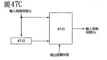
近年來,隨著諸如液晶電視的大尺寸顯示裝置的增長,液晶顯示裝置已經得到實際的發展。尤其是,透過使用由非晶半導體(下文中也稱為非晶矽)形成的電晶體在同一絕緣基板上形成像素電路和包括移位暫存器等的驅動器電路(下文中也稱為內部電路)的技術已經得到實際的發展,因為該技術大幅地促成低功耗和低成本。形成於絕緣基板上的內部電路透過FPC等連接到控制器IC等(下文中也稱為外部電路),且該內部電路的操作得到控制。In recent years, with the growth of large-sized display devices such as liquid crystal televisions, liquid crystal display devices have been actually developed. In particular, a pixel circuit and a driver circuit including a shift register and the like (hereinafter also referred to as an internal circuit) are formed on the same insulating substrate by using a transistor formed of an amorphous semiconductor (hereinafter also referred to as amorphous silicon). ) technology has actually been developed because it contributes significantly to low power consumption and low cost. The internal circuit formed on the insulating substrate is connected to a controller IC or the like (hereinafter also referred to as an external circuit) through an FPC or the like, and the operation of the internal circuit is controlled.
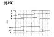
已經在上述內部電路中設計出透過使用由非晶半導體形成的電晶體而形成的移位暫存器(例如,見參考文件1:PCT國際申請No.H10-500243的日文翻譯)。由於在參考文件1中公開的移位暫存器中,輸出端子處於浮置狀態的周期長,因此存在該移位暫存器的輸出信號中容易出現雜訊的問題。為了解決參考文件1中公開的移位暫存器的問題,已經設計出一種其中輸出端子不進入浮置狀態的移位暫存器結構(例如,見參考文件2:2.0 inch a-Si:H TFT-LCD with Low Noise Integrated Gate Driver SID '05 DIGEST pp.942 to 945)。A shift register formed by using a transistor formed of an amorphous semiconductor has been designed in the above-mentioned internal circuit (for example, see Ref.1: Japanese translation of PCT International Application No. H10-500243). Since in the shift register disclosed in
在參考文件2中,連接在輸出端子和負電壓源之間的電晶體在非選擇周期內導通。因此,參考文件2中公開的移位暫存器的輸出端子並不進入浮置狀態,參考文件2中公開的移位暫存器中輸出信號的雜訊因此可以減小。In
然而,已知由非晶半導體形成的電晶體的特性隨電晶體導通時間數量、施加的電壓等而惡化。在惡化的原因中,臨界值電壓發生漂移(增大)的臨界值電壓漂移是移位暫存器失靈的主要原因之一。因此,在參考文件2中公開的移位暫存器中,由於連接在輸出端子和負電壓源之間的電晶體在非選擇周期導通,該移位暫存器由於電晶體特性惡化而失靈。However, it is known that the characteristics of transistors formed of amorphous semiconductors deteriorate with the amount of time the transistor is on, applied voltage, and the like. Among the causes of deterioration, the threshold voltage drift in which the threshold voltage drifts (increases) is one of the main reasons for the failure of the shift register. Therefore, in the shift register disclosed in
鑒於前述問題,本發明的目的是提供一種包括移位暫存器的液晶顯示裝置,其中輸出信號的雜訊在非選擇周期內減小且電晶體特性的惡化可以得到抑制,以及具有該液晶顯示裝置的電子裝置。In view of the foregoing problems, an object of the present invention is to provide a liquid crystal display device including a shift register in which noise of an output signal is reduced in a non-selection period and deterioration of transistor characteristics can be suppressed, and whichElectronic devices for crystal display devices.
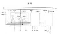
本發明的液晶顯示裝置包括形成於絕緣基板上的像素部以及形成於該絕緣基板上的移位暫存器。此外,該移位暫存器包括多個正反器,且該多個正反器的每一個包括在非選擇周期內按規定時間間隔導通且向輸出端子(掃描線)輸出電源電位的電晶體。該電晶體按規定時間間隔導通並輸出電源電位到該掃描線,使得該多個正反器的每一個抑制了該掃描線的電位波動和該電晶體的特性惡化。The liquid crystal display device of the present invention includes a pixel portion formed on an insulating substrate and a shift register formed on the insulating substrate. In addition, the shift register includes a plurality of flip-flops, and each of the plurality of flip-flops includes a transistor that is turned on at predetermined time intervals during a non-selection period and outputs a power supply potential to an output terminal (scanning line) . The transistor is turned on at prescribed time intervals and outputs a power supply potential to the scan line, so that each of the plurality of flip-flops suppresses the potential fluctuation of the scan line and the deterioration of the characteristics of the transistor.
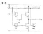
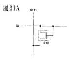
本發明的液晶顯示裝置包括分別具有液晶元件的第一和第二像素、驅動器電路、第一佈線、第二佈線、第三佈線、第四佈線、第五佈線和第六佈線。該第一像素透過該第五佈線電連接到該驅動器電路,且該第二像素透過該第六佈線電連接到該驅動器電路。該驅動器電路包括移位暫存器。該移位暫存器包括多個正反器。該多個正反器的至少一個包括第一電晶體、第二電晶體、第三電晶體和第四電晶體。該第一電晶體的第一端子電連接到該第一佈線;該第一電晶體的第二端子電連接到該第二電晶體的閘極端子;且該第一電晶體的閘極端子電連接到該第五佈線。該第二電晶體的第一端子電連接到該第三佈線,且該第二電晶體的第二端子電連接到第六佈線。該第三電晶體的第一端子電連接到該第二電晶體的閘極端子;該第三電晶體的第二端子電連接到該第二佈線;且該第三電晶體的閘極端子電連接到該第四佈線。該第四電晶體的第一端子電連接到該第六佈線;該第四電晶體的第二端子電連接到該第二佈線;且該第四電晶體的閘極端子電連接到該第四佈線。The liquid crystal display device of the present invention includes first and second pixels each having a liquid crystal element, a driver circuit, a first wiring, a second wiring, a third wiring, a fourth wiring, a fifth wiring and a sixth wiring. The first pixel is electrically connected to the driver circuit through the fifth wiring, and the second pixel is electrically connected to the driver circuit through the sixth wiring. The driver circuit includes a shift register. The shift register includes a plurality of flip-flops. At least one of the plurality of flip-flops includes a first transistor, a second transistor, a third transistor, and a fourth transistor. The first terminal of the first transistor is electrically connected to the first wiring; the second terminal of the first transistor is electrically connected to the gate terminal of the second transistor; and the gate terminal of the first transistor is electrically connected connected to the fifth wiring. The first terminal of the second transistor is electrically connected to the third wiring, and the second terminal of the second transistor is electrically connected to the sixth wiring. The first terminal of the third transistor is electrically connected to the gate terminal of the second transistor; the second terminal of the third transistor is electrically connected to the second wiring; and the gate terminal of the third transistor is electrically connected connected to the fourth wiring. The first terminal of the fourth transistor is electrically connected to the sixth wiring; the second terminal of the fourth transistor is electrically connected to the secondwiring; and the gate terminal of the fourth transistor is electrically connected to the fourth wiring.
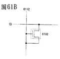
本發明的液晶顯示裝置包括分別具有液晶元件的第一和第二像素、驅動器電路、第一佈線、第二佈線、第三佈線、第四佈線和第五佈線。該第一像素透過該第五佈線電連接到該驅動器電路,且該第二像素透過該第一佈線電連接到該驅動器電路。該驅動器電路包括移位暫存器。該移位暫存器包括多個正反器。該多個正反器的至少一個包括第一電晶體、第二電晶體、第三電晶體和第四電晶體。該第一電晶體的第一端子電連接到該第五佈線;該第一電晶體的第二端子電連接到該第二電晶體的閘極端子;且該第一電晶體的閘極端子電連接到該第五佈線。該第二電晶體的第一端子電連接到該第三佈線,且該第二電晶體的第二端子電連接到第一佈線。該第三電晶體的第一端子電連接到該第二電晶體的閘極端子;該第三電晶體的第二端子電連接到該第二佈線;且該第三電晶體的閘極端子電連接到該第四佈線。該第四電晶體的第一端子電連接到該第一佈線;該第四電晶體的第二端子電連接到該第二佈線;且該第四電晶體的閘極端子電連接到該第四佈線。The liquid crystal display device of the present invention includes first and second pixels each having a liquid crystal element, a driver circuit, a first wiring, a second wiring, a third wiring, a fourth wiring, and a fifth wiring. The first pixel is electrically connected to the driver circuit through the fifth wiring, and the second pixel is electrically connected to the driver circuit through the first wiring. The driver circuit includes a shift register. The shift register includes a plurality of flip-flops. At least one of the plurality of flip-flops includes a first transistor, a second transistor, a third transistor, and a fourth transistor. The first terminal of the first transistor is electrically connected to the fifth wiring; the second terminal of the first transistor is electrically connected to the gate terminal of the second transistor; and the gate terminal of the first transistor is electrically connected connected to the fifth wiring. The first terminal of the second transistor is electrically connected to the third wiring, and the second terminal of the second transistor is electrically connected to the first wiring. The first terminal of the third transistor is electrically connected to the gate terminal of the second transistor; the second terminal of the third transistor is electrically connected to the second wiring; and the gate terminal of the third transistor is electrically connected connected to the fourth wiring. The first terminal of the fourth transistor is electrically connected to the first wiring; the second terminal of the fourth transistor is electrically connected to the second wiring; and the gate terminal of the fourth transistor is electrically connected to the fourth wiring.
注意,在本發明中,該第一電晶體、第二電晶體、第三電晶體和第四電晶體的每一個可以是N通道電晶體。Note that, in the present invention, each of the first transistor, the second transistor, the third transistor, and the fourth transistor may be an N-channel transistor.
此外,在本發明中,該第一電晶體、第二電晶體、第三電晶體和第四電晶體的每一個可具有半導體層且該半導體層可以是非晶矽。Furthermore, in the present invention, each of the first transistor, the second transistor, the third transistor, and the fourth transistor may have a semiconductor layer and the semiconductor layer may be amorphous silicon.
此外,在本發明中,電容器可在該第一電晶體的第二端子和閘極端子之間。In addition, in the present invention, the capacitor may be in the second of the first transistorbetween the terminal and the gate terminal.
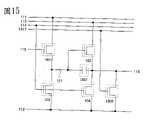
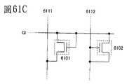
本發明的液晶顯示裝置包括分別具有液晶元件的第一和第二像素、驅動器電路、第一佈線、第二佈線、第三佈線、第四佈線、第五佈線、第六佈線和第七佈線。該第一像素透過該第五佈線電連接到該驅動器電路,且該第二像素透過該第六佈線電連接到該驅動器電路。該驅動器電路包括移位暫存器。該移位暫存器包括多個正反器。該多個正反器的至少一個包括第一電晶體、第二電晶體、第三電晶體、第四電晶體和第五電晶體。該第一電晶體的第一端子電連接到該第一佈線;該第一電晶體的第二端子電連接到該第二電晶體的閘極端子;且該第一電晶體的閘極端子電連接到該第五佈線。該第二電晶體的第一端子電連接到該第三佈線,且該第二電晶體的第二端子電連接到第六佈線。該第三電晶體的第一端子電連接到該第二電晶體的閘極端子;該第三電晶體的第二端子電連接到該第二佈線;且該第三電晶體的閘極端子電連接到該第四佈線。該第四電晶體的第一端子電連接到該第六佈線;該第四電晶體的第二端子電連接到該第二佈線;且該第四電晶體的閘極端子電連接到該第四佈線。該第五電晶體的第一端子電連接到該第六佈線;該第五電晶體的第二端子電連接到該第二佈線;且該第五電晶體的閘極端子電連接到該第七佈線。The liquid crystal display device of the present invention includes first and second pixels each having a liquid crystal element, a driver circuit, a first wiring, a second wiring, a third wiring, a fourth wiring, a fifth wiring, a sixth wiring and a seventh wiring. The first pixel is electrically connected to the driver circuit through the fifth wiring, and the second pixel is electrically connected to the driver circuit through the sixth wiring. The driver circuit includes a shift register. The shift register includes a plurality of flip-flops. At least one of the plurality of flip-flops includes a first transistor, a second transistor, a third transistor, a fourth transistor, and a fifth transistor. The first terminal of the first transistor is electrically connected to the first wiring; the second terminal of the first transistor is electrically connected to the gate terminal of the second transistor; and the gate terminal of the first transistor is electrically connected connected to the fifth wiring. The first terminal of the second transistor is electrically connected to the third wiring, and the second terminal of the second transistor is electrically connected to the sixth wiring. The first terminal of the third transistor is electrically connected to the gate terminal of the second transistor; the second terminal of the third transistor is electrically connected to the second wiring; and the gate terminal of the third transistor is electrically connected connected to the fourth wiring. The first terminal of the fourth transistor is electrically connected to the sixth wiring; the second terminal of the fourth transistor is electrically connected to the second wiring; and the gate terminal of the fourth transistor is electrically connected to the fourth wiring wiring. The first terminal of the fifth transistor is electrically connected to the sixth wiring; the second terminal of the fifth transistor is electrically connected to the second wiring; and the gate terminal of the fifth transistor is electrically connected to the seventh wiring wiring.
本發明的液晶顯示裝置包括分別具有液晶元件的第一和第二像素、驅動器電路、第一佈線、第二佈線、第三佈線、第四佈線、第五佈線和第六佈線。該第一像素透過該第五佈線電連接到該驅動器電路,且該第二像素透過該第一佈線電連接到該驅動器電路。該驅動器電路包括移位暫存器。該移位暫存器包括多個正反器。該多個正反器的至少一個包括第一電晶體、第二電晶體、第三電晶體、第四電晶體和第五電晶體。該第一電晶體的第一端子電連接到該第五佈線;該第一電晶體的第二端子電連接到該第二電晶體的閘極端子;且該第一電晶體的閘極端子電連接到該第五佈線。該第二電晶體的第一端子電連接到該第三佈線,且該第二電晶體的第二端子電連接到第六佈線。該第三電晶體的第一端子電連接到該第二佈線;該第三電晶體的第二端子電連接到該第二電晶體的閘極端子;且該第三電晶體的閘極端子電連接到該第四佈線。該第四電晶體的第一端子電連接到該第六佈線;該第四電晶體的第二端子電連接到該第二佈線;且該第四電晶體的閘極端子電連接到該第四佈線。該第五電晶體的第一端子電連接到該第六佈線;該第五電晶體的第二端子電連接到該第二佈線;且該第五電晶體的閘極端子電連接到該第一佈線。The liquid crystal display device of the present invention includes first and second pixels each having a liquid crystal element, a driver circuit, a first wiring, a second wiring, a third wiring, a fourth wiring, a fifth wiring and a sixth wiring. the first pixel through theThe fifth wiring is electrically connected to the driver circuit, and the second pixel is electrically connected to the driver circuit through the first wiring. The driver circuit includes a shift register. The shift register includes a plurality of flip-flops. At least one of the plurality of flip-flops includes a first transistor, a second transistor, a third transistor, a fourth transistor, and a fifth transistor. The first terminal of the first transistor is electrically connected to the fifth wiring; the second terminal of the first transistor is electrically connected to the gate terminal of the second transistor; and the gate terminal of the first transistor is electrically connected connected to the fifth wiring. The first terminal of the second transistor is electrically connected to the third wiring, and the second terminal of the second transistor is electrically connected to the sixth wiring. The first terminal of the third transistor is electrically connected to the second wiring; the second terminal of the third transistor is electrically connected to the gate terminal of the second transistor; and the gate terminal of the third transistor is electrically connected connected to the fourth wiring. The first terminal of the fourth transistor is electrically connected to the sixth wiring; the second terminal of the fourth transistor is electrically connected to the second wiring; and the gate terminal of the fourth transistor is electrically connected to the fourth wiring wiring. The first terminal of the fifth transistor is electrically connected to the sixth wiring; the second terminal of the fifth transistor is electrically connected to the second wiring; and the gate terminal of the fifth transistor is electrically connected to the first wiring wiring.
注意,在本發明中,該第一電晶體、第二電晶體、第三電晶體、第四電晶體和第五電晶體的每一個可以是N通道電晶體。Note that, in the present invention, each of the first transistor, the second transistor, the third transistor, the fourth transistor, and the fifth transistor may be an N-channel transistor.
此外,在本發明中,該第一電晶體、第二電晶體、第三電晶體、第四電晶體和第五電晶體的每一個可具有半導體層且該半導體層可以是非晶矽。Furthermore, in the present invention, each of the first transistor, the second transistor, the third transistor, the fourth transistor, and the fifth transistor may have a semiconductor layer and the semiconductor layer may be amorphous silicon.
此外,在本發明中,電容器可在該第一電晶體的第二端子和閘極端子之間。In addition, in the present invention, the capacitor may be in the second of the first transistorbetween the terminal and the gate terminal.
本發明的液晶顯示裝置包括分別具有液晶元件的第一至第四像素、第一驅動器電路、第二驅動器電路、第一佈線、第二佈線、第三佈線、第四佈線、第五佈線、第六佈線、第七佈線、第八佈線、第九佈線、第十佈線、第十一佈線和第十二佈線。該第一像素透過該第五佈線電連接到該第一驅動器電路;該第二像素透過該第六佈線電連接到該第一驅動器電路;該第三像素透過該第十一佈線電連接到該第二驅動器電路;且該第四像素透過該第十二佈線電連接到該第二驅動器電路。該第一驅動器電路包括第一移位暫存器,該第二驅動器電路包括第二移位暫存器。該第一移位暫存器包括多個正反器。該多個正反器的至少一個包括第一電晶體、第二電晶體、第三電晶體和第四電晶體。該第一電晶體的第一端子電連接到該第一佈線;該第一電晶體的第二端子電連接到該第二電晶體的閘極端子;且該第一電晶體的閘極端子電連接到該第五佈線。該第二電晶體的第一端子電連接到該第三佈線,且該第二電晶體的第二端子電連接到第六佈線。該第三電晶體的第一端子電連接到該第二佈線;該第三電晶體的第二端子電連接到該第二電晶體的閘極端子;且該第三電晶體的閘極端子電連接到該第四佈線。該第四電晶體的第一端子電連接到該第二佈線;該第四電晶體的第二端子電連接到該第六佈線;且該第四電晶體的閘極端子電連接到該第四佈線。該第二移位暫存器包括多個正反器。該多個正反器的至少一個包括第五電晶體、第六電晶體、第七電晶體和第八電晶體。該第五電晶體的第一端子電連接到該第七佈線;該第五電晶體的第二端子電連接到該第六電晶體的閘極端子;且該第五電晶體的閘極端子電連接到該第十一佈線。該第六電晶體的第一端子電連接到該第九佈線,且該第六電晶體的第二端子電連接到第十二佈線。該第七電晶體的第一端子電連接到該第八佈線;該第七電晶體的第二端子電連接到該第六電晶體的閘極端子;且該第七電晶體的閘極端子電連接到該第十佈線。該第八電晶體的第一端子電連接到該第八佈線;該第八電晶體的第二端子電連接到該第十二佈線;且該第八電晶體的閘極端子電連接到該第十佈線。The liquid crystal display device of the present invention includes first to fourth pixels each having a liquid crystal element, a first driver circuit, a second driver circuit, a first wiring, a second wiring, a third wiring, a fourth wiring, a fifth wiring, a first wiring Sixth wiring, seventh wiring, eighth wiring, ninth wiring, tenth wiring, eleventh wiring, and twelfth wiring. The first pixel is electrically connected to the first driver circuit through the fifth wiring; the second pixel is electrically connected to the first driver circuit through the sixth wiring; the third pixel is electrically connected to the first driver circuit through the eleventh wiring a second driver circuit; and the fourth pixel is electrically connected to the second driver circuit through the twelfth wiring. The first driver circuit includes a first shift register, and the second driver circuit includes a second shift register. The first shift register includes a plurality of flip-flops. At least one of the plurality of flip-flops includes a first transistor, a second transistor, a third transistor, and a fourth transistor. The first terminal of the first transistor is electrically connected to the first wiring; the second terminal of the first transistor is electrically connected to the gate terminal of the second transistor; and the gate terminal of the first transistor is electrically connected connected to the fifth wiring. The first terminal of the second transistor is electrically connected to the third wiring, and the second terminal of the second transistor is electrically connected to the sixth wiring. The first terminal of the third transistor is electrically connected to the second wiring; the second terminal of the third transistor is electrically connected to the gate terminal of the second transistor; and the gate terminal of the third transistor is electrically connected connected to the fourth wiring. The first terminal of the fourth transistor is electrically connected to the second wiring; the second terminal of the fourth transistor is electrically connected to the sixth wiring; and the gate terminal of the fourth transistor is electrically connected to the fourth wiring wiring. The second shift register includes a plurality of flip-flops. at least one of the plurality of flip-flopsEach includes a fifth transistor, a sixth transistor, a seventh transistor, and an eighth transistor. The first terminal of the fifth transistor is electrically connected to the seventh wiring; the second terminal of the fifth transistor is electrically connected to the gate terminal of the sixth transistor; and the gate terminal of the fifth transistor is electrically connected connected to the eleventh wiring. The first terminal of the sixth transistor is electrically connected to the ninth wiring, and the second terminal of the sixth transistor is electrically connected to the twelfth wiring. The first terminal of the seventh transistor is electrically connected to the eighth wiring; the second terminal of the seventh transistor is electrically connected to the gate terminal of the sixth transistor; and the gate terminal of the seventh transistor is electrically connected connected to the tenth wiring. The first terminal of the eighth transistor is electrically connected to the eighth wiring; the second terminal of the eighth transistor is electrically connected to the twelfth wiring; and the gate terminal of the eighth transistor is electrically connected to the twelfth wiring Ten wiring.
注意,在本發明中,該第五佈線和該第十一佈線可以電連接,該第六佈線和該第十二佈線可以電連接。Note that, in the present invention, the fifth wiring and the eleventh wiring may be electrically connected, and the sixth wiring and the twelfth wiring may be electrically connected.
注意,在本發明中,該第五佈線和該第十一佈線可以是相同佈線,該第六佈線和該第十二佈線可以是相同佈線。Note that, in the present invention, the fifth wiring and the eleventh wiring may be the same wiring, and the sixth wiring and the twelfth wiring may be the same wiring.
注意,在本發明中,該第一佈線和該第七佈線可以電連接;該第二佈線和該第八佈線可以電連接;該第三佈線和該第九佈線可以電連接;且該第四佈線和該第十佈線可以電連接。Note that in the present invention, the first wiring and the seventh wiring may be electrically connected; the second wiring and the eighth wiring may be electrically connected; the third wiring and the ninth wiring may be electrically connected; and the fourth wiring The wiring and the tenth wiring may be electrically connected.
注意,在本發明中,該第一佈線和該第七佈線可以是相同佈線;該第二佈線和該第八佈線可以是相同佈線;該第三佈線和該第九佈線可以是相同佈線;且該第四佈線和該第十佈線可以是相同佈線。Note that in the present invention, the first wiring and the seventh wiring may be the same wiring; the second wiring and the eighth wiring may be the same wiring; the third wiring and the ninth wiring may be the same wiring; and The fourth wiring andThe tenth wiring may be the same wiring.
注意,在本發明中,該第一佈線和該第七佈線可以電連接;該第二佈線和該第八佈線可以電連接;該第三佈線和該第九佈線可以電連接;該第四佈線和該第十佈線可以電連接;該第五佈線和該第十一佈線可以電連接;且該第六佈線和該第十二佈線可以電連接。Note that in the present invention, the first wiring and the seventh wiring may be electrically connected; the second wiring and the eighth wiring may be electrically connected; the third wiring and the ninth wiring may be electrically connected; the fourth wiring and the tenth wiring may be electrically connected; the fifth wiring and the eleventh wiring may be electrically connected; and the sixth wiring and the twelfth wiring may be electrically connected.
注意,在本發明中,該第一佈線和該第七佈線可以是相同佈線;該第二佈線和該第八佈線可以是相同佈線;該第三佈線和該第九佈線可以是相同佈線;該第四佈線和該第十佈線可以是相同佈線;該第五佈線和該第十一佈線可以是相同佈線;且該第六佈線和該第十二佈線可以是相同佈線。Note that in the present invention, the first wiring and the seventh wiring may be the same wiring; the second wiring and the eighth wiring may be the same wiring; the third wiring and the ninth wiring may be the same wiring; the The fourth wiring and the tenth wiring may be the same wiring; the fifth wiring and the eleventh wiring may be the same wiring; and the sixth wiring and the twelfth wiring may be the same wiring.
本發明的液晶顯示裝置包括分別具有液晶元件的第一至第四像素、第一驅動器電路、第二驅動器電路、第一佈線、第二佈線、第三佈線、第四佈線、第五佈線、第六佈線、第七佈線、第八佈線、第九佈線和第十佈線。該第一像素透過該第五佈線電連接到該第一驅動器電路;該第二像素透過該第一佈線電連接到該第一驅動器電路;該第三像素透過該第十佈線電連接到該第二驅動器電路;且該第四像素透過該第六佈線電連接到該第二驅動器電路。該第一驅動器電路包括第一移位暫存器,該第二驅動器電路包括第二移位暫存器。該第一移位暫存器包括多個正反器。該多個正反器的至少一個包括第一電晶體、第二電晶體、第三電晶體和第四電晶體。該第一電晶體的第一端子電連接到該第五佈線;該第一電晶體的第二端子電連接到該第二電晶體的閘極端子;且該第一電晶體的閘極端子電連接到該第五佈線。該第二電晶體的第一端子電連接到該第三佈線,且該第二電晶體的第二端子電連接到第一佈線。該第三電晶體的第一端子電連接到該第二電晶體的閘極端子;該第三電晶體的第二端子電連接到該第二佈線;且該第三電晶體的閘極端子電連接到該第四佈線。該第四電晶體的第一端子電連接到該第一佈線;該第四電晶體的第二端子電連接到該第二佈線;且該第四電晶體的閘極端子電連接到該第四佈線。該第二移位暫存器包括多個正反器。該多個正反器的至少一個包括第五電晶體、第六電晶體、第七電晶體和第八電晶體。該第五電晶體的第一端子電連接到該第十佈線;該第五電晶體的第二端子電連接到該第六電晶體的閘極端子;且該第五電晶體的閘極端子電連接到該第十佈線。該第六電晶體的第一端子電連接到該第八佈線,且該第六電晶體的第二端子電連接到第六佈線。該第七電晶體的第一端子電連接到該第六電晶體的閘極端子;該第七電晶體的第二端子電連接到該第七佈線;且該第七電晶體的閘極端子電連接到該第九佈線。該第八電晶體的第一端子電連接到該第六佈線;該第八電晶體的第二端子電連接到該第七佈線;且該第八電晶體的閘極端子電連接到該第九佈線。The liquid crystal display device of the present invention includes first to fourth pixels each having a liquid crystal element, a first driver circuit, a second driver circuit, a first wiring, a second wiring, a third wiring, a fourth wiring, a fifth wiring, a first wiring Sixth wiring, seventh wiring, eighth wiring, ninth wiring, and tenth wiring. The first pixel is electrically connected to the first driver circuit through the fifth wiring; the second pixel is electrically connected to the first driver circuit through the first wiring; the third pixel is electrically connected to the first driver circuit through the tenth wiring two driver circuits; and the fourth pixel is electrically connected to the second driver circuit through the sixth wiring. The first driver circuit includes a first shift register, and the second driver circuit includes a second shift register. The first shift register includes a plurality of flip-flops. At least one of the plurality of flip-flops includes a first transistor, a second transistor, a third transistor, and a fourth transistor. The first terminal of the first transistor is electrically connectedconnected to the fifth wiring; the second terminal of the first transistor is electrically connected to the gate terminal of the second transistor; and the gate terminal of the first transistor is electrically connected to the fifth wiring. The first terminal of the second transistor is electrically connected to the third wiring, and the second terminal of the second transistor is electrically connected to the first wiring. The first terminal of the third transistor is electrically connected to the gate terminal of the second transistor; the second terminal of the third transistor is electrically connected to the second wiring; and the gate terminal of the third transistor is electrically connected connected to the fourth wiring. The first terminal of the fourth transistor is electrically connected to the first wiring; the second terminal of the fourth transistor is electrically connected to the second wiring; and the gate terminal of the fourth transistor is electrically connected to the fourth wiring. The second shift register includes a plurality of flip-flops. At least one of the plurality of flip-flops includes a fifth transistor, a sixth transistor, a seventh transistor, and an eighth transistor. The first terminal of the fifth transistor is electrically connected to the tenth wiring; the second terminal of the fifth transistor is electrically connected to the gate terminal of the sixth transistor; and the gate terminal of the fifth transistor is electrically connected connected to the tenth wiring. The first terminal of the sixth transistor is electrically connected to the eighth wiring, and the second terminal of the sixth transistor is electrically connected to the sixth wiring. The first terminal of the seventh transistor is electrically connected to the gate terminal of the sixth transistor; the second terminal of the seventh transistor is electrically connected to the seventh wiring; and the gate terminal of the seventh transistor is electrically connected connected to the ninth wiring. The first terminal of the eighth transistor is electrically connected to the sixth wiring; the second terminal of the eighth transistor is electrically connected to the seventh wiring; and the gate terminal of the eighth transistor is electrically connected to the ninth wiring wiring.
注意,在本發明中,該第一佈線和該第六佈線可以電連接,該第五佈線和該第十佈線可以電連接。Note that, in the present invention, the first wiring and the sixth wiring may be electrically connected, and the fifth wiring and the tenth wiring may be electrically connected.
注意,在本發明中,該第一佈線和該第六佈線可以是相同佈線,該第五佈線和該第十佈線可以是相同佈線。Note that, in the present invention, the first wiring and the sixth wiring may be the same wiring, and the fifth wiring and the tenth wiring may be the same wiring.
此外,在本發明中,該第二佈線和該第七佈線可以電連接;該第三佈線和該第八佈線可以電連接;且該第四佈線和該第九佈線可以電連接。Further, in the present invention, the second wiring and the seventh wiring may be electrically connected; the third wiring and the eighth wiring may be electrically connected; and the fourth wiring and the ninth wiring may be electrically connected.
此外,在本發明中,該第二佈線和該第七佈線可以是相同佈線;該第三佈線和該第八佈線可以是相同佈線;且該第四佈線和該第九佈線可以是相同佈線。Furthermore, in the present invention, the second wiring and the seventh wiring may be the same wiring; the third wiring and the eighth wiring may be the same wiring; and the fourth wiring and the ninth wiring may be the same wiring.
此外,在本發明中,該第一佈線和該第六佈線可以電連接;該第二佈線和該第七佈線可以電連接;該第三佈線和該第八佈線可以電連接;該第四佈線和該第九佈線可以電連接;且該第五佈線和該第十佈線可以電連接。Further, in the present invention, the first wiring and the sixth wiring may be electrically connected; the second wiring and the seventh wiring may be electrically connected; the third wiring and the eighth wiring may be electrically connected; the fourth wiring and the ninth wiring can be electrically connected; and the fifth wiring and the tenth wiring can be electrically connected.
注意,在本發明中,該第一佈線和該第六佈線可以是相同佈線;該第二佈線和該第七佈線可以是相同佈線;該第三佈線和該第八佈線可以是相同佈線;該第四佈線和該第九佈線可以是相同佈線;且該第五佈線和該第十佈線可以是相同佈線。Note that in the present invention, the first wiring and the sixth wiring may be the same wiring; the second wiring and the seventh wiring may be the same wiring; the third wiring and the eighth wiring may be the same wiring; the The fourth wiring and the ninth wiring may be the same wiring; and the fifth wiring and the tenth wiring may be the same wiring.
此外,在本發明中,該第一電晶體、第二電晶體、第三電晶體、第四電晶體、第五電晶體、第六電晶體、第七電晶體和第八電晶體的每一個可以是N通道電晶體。Further, in the present invention, each of the first transistor, the second transistor, the third transistor, the fourth transistor, the fifth transistor, the sixth transistor, the seventh transistor, and the eighth transistor Can be an N-channel transistor.
此外,在本發明中,該第一電晶體、第二電晶體、第三電晶體、第四電晶體、第五電晶體、第六電晶體、第七電晶體和第八電晶體的每一個可具有半導體層且該半導體層可以是非晶矽。Further, in the present invention, each of the first transistor, the second transistor, the third transistor, the fourth transistor, the fifth transistor, the sixth transistor, the seventh transistor, and the eighth transistor There may be a semiconductor layer and the semiconductor layer may be amorphous silicon.
此外,在本發明中,第一電容器可提供於該第一電晶體的第二端子和閘極端子之間,且第二電容器可提供於該第五電晶體的第二端子和閘極端子之間。Furthermore, in the present invention, a first capacitor may be provided between the second terminal and the gate terminal of the first transistor, and a second capacitor may be provided between the second terminal and the gate terminal of the fifth transistor between.
本發明的液晶顯示裝置包括分別具有液晶元件的第一至第四像素、第一驅動器電路、第二驅動器電路、第一佈線、第二佈線、第三佈線、第四佈線、第五佈線、第六佈線、第七佈線、第八佈線、第九佈線、第十佈線、第十一佈線、第十二佈線、第十三佈線和第十四佈線。該第一像素透過該第五佈線電連接到該第一驅動器電路;該第二像素透過該第六佈線電連接到該第一驅動器電路;該第三像素透過該第十二佈線電連接到該第二驅動器電路;且該第四像素透過該第十三佈線電連接到該第二驅動器電路。該第一驅動器電路包括第一移位暫存器,該第二驅動器電路包括第二移位暫存器。該第一移位暫存器包括多個正反器。該多個正反器的至少一個包括第一電晶體、第二電晶體、第三電晶體、第四電晶體和第五電晶體。該第一電晶體的第一端子電連接到該第一佈線;該第一電晶體的第二端子電連接到該第二電晶體的閘極端子;且該第一電晶體的閘極端子電連接到該第五佈線。該第二電晶體的第一端子電連接到該第三佈線,且該第二電晶體的第二端子電連接到第六佈線。該第三電晶體的第一端子電連接到該第二佈線;該第三電晶體的第二端子電連接到該第二電晶體的閘極端子;且該第三電晶體的閘極端子電連接到該第四佈線。該第四電晶體的第一端子電連接到該第二佈線;該第四電晶體的第二端子電連接到該第六佈線;且該第四電晶體的閘極端子電連接到該第四佈線。該第五電晶體的第一端子電連接到該第二佈線;該第五電晶體的第二端子電連接到該第六佈線;且該第五電晶體的閘極端子電連接到該第七佈線。該第二移位暫存器包括多個正反器。該多個正反器的至少一個包括第六電晶體、第七電晶體、第八電晶體、第九電晶體和第十電晶體。該第六電晶體的第一端子電連接到該第八佈線;該第六電晶體的第二端子電連接到該第七電晶體的閘極端子;且該第六電晶體的閘極端子電連接到該第十二佈線。該第七電晶體的第一端子電連接到該第十佈線,且該第七電晶體的第二端子電連接到第十三佈線。該第八電晶體的第一端子電連接到該第九佈線;該第八電晶體的第二端子電連接到該第七電晶體的閘極端子;且該第八電晶體的閘極端子電連接到該第十一佈線。該第九電晶體的第一端子電連接到該第十三佈線;該第九電晶體的第二端子電連接到該第九佈線;且該第九電晶體的閘極端子電連接到該第十一佈線。該第十電晶體的第一端子電連接到該第十三佈線;該第十電晶體的第二端子電連接到該第九佈線;且該第十電晶體的閘極端子電連接到該第十四佈線。The liquid crystal display device of the present invention includes first to fourth pixels each having a liquid crystal element, a first driver circuit, a second driver circuit, a first wiring, a second wiring, a third wiring, a fourth wiring, a fifth wiring, a first wiring Sixth wiring, seventh wiring, eighth wiring, ninth wiring, tenth wiring, eleventh wiring, twelfth wiring, thirteenth wiring, and fourteenth wiring. The first pixel is electrically connected to the first driver circuit via the fifth wiring; the second pixel is electrically connected to the first driver circuit via the sixth wiring; the third pixel is electrically connected to the first driver circuit via the twelfth wiring a second driver circuit; and the fourth pixel is electrically connected to the second driver circuit through the thirteenth wiring. The first driver circuit includes a first shift register, and the second driver circuit includes a second shift register. The first shift register includes a plurality of flip-flops. At least one of the plurality of flip-flops includes a first transistor, a second transistor, a third transistor, a fourth transistor, and a fifth transistor. The first terminal of the first transistor is electrically connected to the first wiring; the second terminal of the first transistor is electrically connected to the gate terminal of the second transistor; and the gate terminal of the first transistor is electrically connected connected to the fifth wiring. The first terminal of the second transistor is electrically connected to the third wiring, and the second terminal of the second transistor is electrically connected to the sixth wiring. The first terminal of the third transistor is electrically connected to the second wiring; the second terminal of the third transistor is electrically connected to the gate terminal of the second transistor; and the gate terminal of the third transistor is electrically connected connected to the fourth wiring. The first terminal of the fourth transistor is electrically connected to the second wiring; the first terminalThe second terminal of the quad transistor is electrically connected to the sixth wiring; and the gate terminal of the fourth transistor is electrically connected to the fourth wiring. The first terminal of the fifth transistor is electrically connected to the second wiring; the second terminal of the fifth transistor is electrically connected to the sixth wiring; and the gate terminal of the fifth transistor is electrically connected to the seventh wiring wiring. The second shift register includes a plurality of flip-flops. At least one of the plurality of flip-flops includes a sixth transistor, a seventh transistor, an eighth transistor, a ninth transistor, and a tenth transistor. The first terminal of the sixth transistor is electrically connected to the eighth wiring; the second terminal of the sixth transistor is electrically connected to the gate terminal of the seventh transistor; and the gate terminal of the sixth transistor is electrically connected connected to the twelfth wiring. The first terminal of the seventh transistor is electrically connected to the tenth wiring, and the second terminal of the seventh transistor is electrically connected to the thirteenth wiring. The first terminal of the eighth transistor is electrically connected to the ninth wiring; the second terminal of the eighth transistor is electrically connected to the gate terminal of the seventh transistor; and the gate terminal of the eighth transistor is electrically connected connected to the eleventh wiring. The first terminal of the ninth transistor is electrically connected to the thirteenth wiring; the second terminal of the ninth transistor is electrically connected to the ninth wiring; and the gate terminal of the ninth transistor is electrically connected to the thirteenth wiring Eleven wiring. The first terminal of the tenth transistor is electrically connected to the thirteenth wiring; the second terminal of the tenth transistor is electrically connected to the ninth wiring; and the gate terminal of the tenth transistor is electrically connected to the thirteenth wiring Fourteen wiring.
注意,在本發明中,該第五佈線和該第十二佈線可以電連接,該第六佈線和該第十三佈線可以電連接。Note that, in the present invention, the fifth wiring and the twelfth wiring may be electrically connected, and the sixth wiring and the thirteenth wiring may be electrically connected.
注意,在本發明中,該第五佈線和該第十二佈線可以是相同佈線,該第六佈線和該第十三佈線可以是相同佈線。Note that in the present invention, the fifth wiring and the twelfth wiring may be the same wiring, and the sixth wiring and the thirteenth wiring may be the same wiringString.
此外,在本發明中,該第一佈線和該第八佈線可以電連接;該第二佈線和該第九佈線可以電連接;該第三佈線和該第十佈線可以電連接;該第四佈線和該第十一佈線可以電連接;且該第七佈線和該第十四佈線可以電連接。Furthermore, in the present invention, the first wiring and the eighth wiring may be electrically connected; the second wiring and the ninth wiring may be electrically connected; the third wiring and the tenth wiring may be electrically connected; the fourth wiring and the eleventh wiring can be electrically connected; and the seventh wiring and the fourteenth wiring can be electrically connected.
注意,在本發明中,該第一佈線和該第八佈線可以是相同佈線;該第二佈線和該第九佈線可以是相同佈線;該第三佈線和該第十佈線可以是相同佈線;該第四佈線和該第十一佈線可以是相同佈線;且該第七佈線和該第十四佈線可以是相同佈線。Note that in the present invention, the first wiring and the eighth wiring may be the same wiring; the second wiring and the ninth wiring may be the same wiring; the third wiring and the tenth wiring may be the same wiring; the The fourth wiring and the eleventh wiring may be the same wiring; and the seventh wiring and the fourteenth wiring may be the same wiring.
此外,在本發明中,該第一佈線和該第八佈線可以電連接;該第二佈線和該第九佈線可以電連接;該第三佈線和該第十佈線可以電連接;該第四佈線和該第十一佈線可以電連接;該第五佈線和該第十二佈線可以電連接;該第六佈線和該第十三佈線可以電連接;且該第七佈線和該第十四佈線可以電連接。Furthermore, in the present invention, the first wiring and the eighth wiring may be electrically connected; the second wiring and the ninth wiring may be electrically connected; the third wiring and the tenth wiring may be electrically connected; the fourth wiring and the eleventh wiring may be electrically connected; the fifth wiring and the twelfth wiring may be electrically connected; the sixth wiring and the thirteenth wiring may be electrically connected; and the seventh wiring and the fourteenth wiring may be electrically connected electrical connection.
此外,在本發明中,該第一佈線和該第八佈線可以是相同佈線;該第二佈線和該第九佈線可以是相同佈線;該第三佈線和該第十佈線可以是相同佈線;該第四佈線和該第十一佈線可以是相同佈線;該第五佈線和該第十二佈線可以是相同佈線;該第六佈線和該第十三佈線可以是相同佈線;且該第七佈線和該第十四佈線可以是相同佈線。Furthermore, in the present invention, the first wiring and the eighth wiring may be the same wiring; the second wiring and the ninth wiring may be the same wiring; the third wiring and the tenth wiring may be the same wiring; the The fourth wiring and the eleventh wiring may be the same wiring; the fifth wiring and the twelfth wiring may be the same wiring; the sixth wiring and the thirteenth wiring may be the same wiring; and the seventh wiring and The fourteenth wiring may be the same wiring.
本發明的液晶顯示裝置包括分別具有液晶元件的第一至第四像素、第一驅動器電路、第二驅動器電路、第一佈線、第二佈線、第三佈線、第四佈線、第五佈線、第六佈線、第七佈線、第八佈線、第九佈線、第十佈線、第十一佈線和第十二佈線。該第一像素透過該第五佈線電連接到該第一驅動器電路;該第二像素透過該第六佈線電連接到該第一驅動器電路;該第三像素透過該第十一佈線電連接到該第二驅動器電路;且該第四像素透過該第十二佈線電連接到該第二驅動器電路。該第一驅動器電路包括第一移位暫存器,該第二驅動器電路包括第二移位暫存器。該第一移位暫存器包括多個正反器。該多個正反器的至少一個包括第一電晶體、第二電晶體、第三電晶體、第四電晶體和第五電晶體。該第一電晶體的第一端子電連接到該第五佈線;該第一電晶體的第二端子電連接到該第二電晶體的閘極端子;且該第一電晶體的閘極端子電連接到該第五佈線。該第二電晶體的第一端子電連接到該第三佈線,且該第二電晶體的第二端子電連接到第六佈線。該第三電晶體的第一端子電連接到該第二電晶體的閘極端子;該第三電晶體的第二端子電連接到該第二佈線;且該第三電晶體的閘極端子電連接到該第四佈線。該第四電晶體的第一端子電連接到該第六佈線;該第四電晶體的第二端子電連接到該第二佈線;且該第四電晶體的閘極端子電連接到該第四佈線。該第五電晶體的第一端子電連接到該第六佈線;該第五電晶體的第二端子電連接到該第二佈線;且該第五電晶體的閘極端子電連接到該第一佈線。該第二移位暫存器包括多個正反器。該多個正反器的至少一個包括第六電晶體、第七電晶體、第八電晶體、第九電晶體和第十電晶體。該第六電晶體的第一端子電連接到該第十一佈線;該第六電晶體的第二端子電連接到該第七電晶體的閘極端子;且該第六電晶體的閘極端子電連接到該第十一佈線。該第七電晶體的第一端子電連接到該第九佈線,且該第七電晶體的第二端子電連接到第十二佈線。該第八電晶體的第一端子電連接到該第八佈線;該第八電晶體的第二端子電連接到該第七電晶體的閘極端子;且該第八電晶體的閘極端子電連接到該第十佈線。該第九電晶體的第一端子電連接到該第八佈線;該第九電晶體的第二端子電連接到該第十二佈線;且該第九電晶體的閘極端子電連接到該第十佈線。該第十電晶體的第一端子電連接到該第八佈線;該第十電晶體的第二端子電連接到該第十二佈線;且該第十電晶體的閘極端子電連接到該第七佈線。The liquid crystal display device of the present invention includes first to fourth pixels each having a liquid crystal element, a first driver circuit, a second driver circuit, a first clothLine, second wiring, third wiring, fourth wiring, fifth wiring, sixth wiring, seventh wiring, eighth wiring, ninth wiring, tenth wiring, eleventh wiring, and twelfth wiring. The first pixel is electrically connected to the first driver circuit through the fifth wiring; the second pixel is electrically connected to the first driver circuit through the sixth wiring; the third pixel is electrically connected to the first driver circuit through the eleventh wiring a second driver circuit; and the fourth pixel is electrically connected to the second driver circuit through the twelfth wiring. The first driver circuit includes a first shift register, and the second driver circuit includes a second shift register. The first shift register includes a plurality of flip-flops. At least one of the plurality of flip-flops includes a first transistor, a second transistor, a third transistor, a fourth transistor, and a fifth transistor. The first terminal of the first transistor is electrically connected to the fifth wiring; the second terminal of the first transistor is electrically connected to the gate terminal of the second transistor; and the gate terminal of the first transistor is electrically connected connected to the fifth wiring. The first terminal of the second transistor is electrically connected to the third wiring, and the second terminal of the second transistor is electrically connected to the sixth wiring. The first terminal of the third transistor is electrically connected to the gate terminal of the second transistor; the second terminal of the third transistor is electrically connected to the second wiring; and the gate terminal of the third transistor is electrically connected connected to the fourth wiring. The first terminal of the fourth transistor is electrically connected to the sixth wiring; the second terminal of the fourth transistor is electrically connected to the second wiring; and the gate terminal of the fourth transistor is electrically connected to the fourth wiring wiring. The first terminal of the fifth transistor is electrically connected to the sixth wiring; the second terminal of the fifth transistor is electrically connected to the second wiring; and the gate terminal of the fifth transistor is electrically connected to the first wiring wiring. The second shift register includes a plurality of flip-flops. At least one of the plurality of flip-flops includes a sixth transistorbody, seventh transistor, eighth transistor, ninth transistor and tenth transistor. The first terminal of the sixth transistor is electrically connected to the eleventh wiring; the second terminal of the sixth transistor is electrically connected to the gate terminal of the seventh transistor; and the gate terminal of the sixth transistor Electrically connected to the eleventh wiring. The first terminal of the seventh transistor is electrically connected to the ninth wiring, and the second terminal of the seventh transistor is electrically connected to the twelfth wiring. The first terminal of the eighth transistor is electrically connected to the eighth wiring; the second terminal of the eighth transistor is electrically connected to the gate terminal of the seventh transistor; and the gate terminal of the eighth transistor is electrically connected connected to the tenth wiring. The first terminal of the ninth transistor is electrically connected to the eighth wiring; the second terminal of the ninth transistor is electrically connected to the twelfth wiring; and the gate terminal of the ninth transistor is electrically connected to the twelfth wiring Ten wiring. The first terminal of the tenth transistor is electrically connected to the eighth wiring; the second terminal of the tenth transistor is electrically connected to the twelfth wiring; and the gate terminal of the tenth transistor is electrically connected to the twelfth wiring Seven wiring.
注意,在本發明中,該第五佈線和該第十一佈線可以電連接,該第六佈線和該第十二佈線可以電連接。Note that, in the present invention, the fifth wiring and the eleventh wiring may be electrically connected, and the sixth wiring and the twelfth wiring may be electrically connected.
注意,在本發明中,該第五佈線和該第十一佈線可以是相同佈線,該第六佈線和該第十二佈線可以是相同佈線。Note that, in the present invention, the fifth wiring and the eleventh wiring may be the same wiring, and the sixth wiring and the twelfth wiring may be the same wiring.
此外,在本發明中,該第一佈線和該第七佈線可以電連接;該第二佈線和該第八佈線可以電連接;該第三佈線和該第九佈線可以電連接;且該第四佈線和該第十佈線可以電連接。Furthermore, in the present invention, the first wiring and the seventh wiring may be electrically connected; the second wiring and the eighth wiring may be electrically connected; the third wiring and the ninth wiring may be electrically connected; and the fourth wiring may be electrically connected The wiring and the tenth wiring may be electrically connected.
此外,在本發明中,該第一佈線和該第七佈線可以是相同佈線;該第二佈線和該第八佈線可以是相同佈線;該第三佈線和該第九佈線可以是相同佈線;且該第四佈線和該第十佈線可以是相同佈線。Furthermore, in the present invention, the first wiring and the seventh wiring may bethe same wiring; the second wiring and the eighth wiring may be the same wiring; the third wiring and the ninth wiring may be the same wiring; and the fourth wiring and the tenth wiring may be the same wiring.
此外,在本發明中,該第一佈線和該第七佈線可以電連接;該第二佈線和該第八佈線可以電連接;該第三佈線和該第九佈線可以電連接;該第四佈線和該第十佈線可以電連接;該第五佈線和該第十一佈線可以電連接;且該第六佈線和該第十二佈線可以電連接。Furthermore, in the present invention, the first wiring and the seventh wiring may be electrically connected; the second wiring and the eighth wiring may be electrically connected; the third wiring and the ninth wiring may be electrically connected; the fourth wiring and the tenth wiring may be electrically connected; the fifth wiring and the eleventh wiring may be electrically connected; and the sixth wiring and the twelfth wiring may be electrically connected.
注意,在本發明中,該第一佈線和該第七佈線可以是相同佈線;該第二佈線和該第八佈線可以是相同佈線;該第三佈線和該第九佈線可以是相同佈線;該第四佈線和該第十佈線可以是相同佈線;該第五佈線和該第十一佈線可以是相同佈線;且該第六佈線和該第十二佈線可以是相同佈線。Note that in the present invention, the first wiring and the seventh wiring may be the same wiring; the second wiring and the eighth wiring may be the same wiring; the third wiring and the ninth wiring may be the same wiring; the The fourth wiring and the tenth wiring may be the same wiring; the fifth wiring and the eleventh wiring may be the same wiring; and the sixth wiring and the twelfth wiring may be the same wiring.
注意,在本發明中,該第一電晶體、第二電晶體、第三電晶體、第四電晶體、第五電晶體、第六電晶體、第七電晶體、第八電晶體、第九電晶體和第十電晶體的每一個可以是N通道電晶體。Note that in the present invention, the first transistor, the second transistor, the third transistor, the fourth transistor, the fifth transistor, the sixth transistor, the seventh transistor, the eighth transistor, the ninth transistor Each of the transistor and the tenth transistor may be an N-channel transistor.
注意,在本發明中,該第一電晶體、第二電晶體、第三電晶體、第四電晶體、第五電晶體、第六電晶體、第七電晶體、第八電晶體、第九電晶體和第十電晶體的每一個可具有半導體層且該半導體層可以是非晶矽。Note that in the present invention, the first transistor, the second transistor, the third transistor, the fourth transistor, the fifth transistor, the sixth transistor, the seventh transistor, the eighth transistor, the ninth transistor Each of the transistor and the tenth transistor may have a semiconductor layer and the semiconductor layer may be amorphous silicon.
注意,在本發明中,第一電容器可在該第一電晶體的第二端子和閘極端子之間,且第二電容器可在該第六電晶體的第二端子和閘極端子之間。Note that in the present invention, the first capacitor may be between the second terminal and the gate terminal of the first transistor, and the second capacitor may be between the sixth transistorbetween the second terminal of the body and the gate terminal.
本發明包括具有任一上述液晶顯示裝置的電子裝置。The present invention includes electronic devices having any of the above-described liquid crystal display devices.
注意,各種類型的開關可以作為本說明書中所示的開關,且電學開關、機械開關等可以給出作為示例。也就是說,可以使用任意的元件而不限於特定的元件,只要該元件能夠控制電流流動即可。例如,該開關可以是電晶體、二極體(例如,PN二極體、PIN二極體、肖特基二極體、或者連接成二極體的電晶體)、晶閘管、或者組合這些元件的邏輯電路。對於使用電晶體作為開關的情形,電晶體的極性(導電類型)不具體限於特定類型,因為該電晶體僅僅作為開關。然而,當截止電流較佳是小的時,較佳的使用具有更小截止電流的極性的電晶體。具有更小截止電流的電晶體的示例為設有LDD區的電晶體、具有多個閘極結構的電晶體等。此外,當作為開關的電晶體的源極端子的電位更接近低電位側電源(例如,Vss、GND或0V)時,較佳的使用N通道電晶體,而當源極端子的電位更接近高電位側電源(例如,Vdd)時,較佳的使用P通道電晶體。這是因為該電晶體的閘極-源極電壓絕對值增大,使得該電晶體可以更準確地作為開關。Note that various types of switches can be used as the switches shown in this specification, and electrical switches, mechanical switches, and the like can be given as examples. That is, any element can be used without being limited to a specific element as long as the element can control the flow of current. For example, the switch may be a transistor, a diode (eg, a PN diode, a PIN diode, a Schottky diode, or a transistor connected as a diode), a thyristor, or a combination of these elements. logic circuit. In the case of using a transistor as a switch, the polarity (conductivity type) of the transistor is not particularly limited to a specific type because the transistor acts only as a switch. However, when the off-current is preferably small, it is preferable to use a transistor having a polarity with a smaller off-current. Examples of transistors with smaller off-current are transistors provided with LDD regions, transistors with multiple gate structures, and the like. Furthermore, it is preferable to use an N-channel transistor when the potential of the source terminal of the transistor as the switch is closer to the low potential side power supply (eg, Vss, GND, or 0V), and when the potential of the source terminal is closer to the high potential For potential-side power supply (eg, Vdd), a P-channel transistor is preferably used. This is because the absolute value of the gate-source voltage of the transistor increases, allowing the transistor to act as a switch more accurately.
注意,透過均使用N通道和P通道電晶體,則可以採用CMOS開關。透過採用CMOS開關,則該開關可更精確地作為開關,因為當P通道開關或N通道開關導通時電流可以流過該開關。例如,可以恰當地輸出電壓,而與該開關的輸入信號的電壓是高還是低無關。此外,由於可以使用於導通或截止開關的電壓幅值小,因此可以減小功耗。另外注意,當電晶體用作開關時,該開關包括輸入端子(源極端子和汲極端子之一)、輸出端子(該源極端子和汲極端子的另一個)、和用於控制電傳導的端子(閘極端子)。另一方面,當二極體用作開關時,在某些情況下該開關不具有用於控制電傳導的端子。因此,用於控制端子的佈線的數目可以減少。Note that CMOS switches can be used by using both N-channel and P-channel transistors. By using a CMOS switch, the switch can act more precisely as a switch because current can flow through the switch when either the P-channel switch or the N-channel switch is on. For example, the voltage can be appropriately output regardless of whether the voltage of the input signal to the switch is high or low. Furthermore, sinceThe magnitude of the voltage used to turn the switch on or off can be made small, thus reducing power consumption. Also note that when a transistor is used as a switch, the switch includes an input terminal (one of the source and drain terminals), an output terminal (the other of the source and drain terminals), and controls for electrical conduction terminal (gate terminal). On the other hand, when a diode is used as a switch, in some cases the switch does not have terminals for controlling electrical conduction. Therefore, the number of wirings for the control terminals can be reduced.
注意在本說明書中,“連接”這一描述包括元件電連接的情形,元件功能連接的情形,以及元件直接連接的情形。因此,在本說明書公開的結構中,另一元件可以夾置在具有預定連接關係的元件之間。例如,使得可以電連接的一個或多個元件(例如,開關、電晶體、電容器、電感器、電阻器與/或二極體)可以提供於特定部分和另一部分之間。此外,使得可以功能連接的一個或多個電路可以提供於這些部分之間,例如邏輯電路(例如,反相器、NAND電路或NOR電路)、信號轉換器電路(例如,DA轉換器電路、AD轉換器電路或者灰度校正電路)、電位位準轉換器電路(例如,諸如升壓電路或降壓控制電路的電源電路、或者用於改變高位準信號或低位準信號的電位位準的位準移位電路)、電壓源、電流源、開關電路、或者放大器電路(例如,可以增大信號振幅、電流量等的電路,諸如運算放大器、差分發電器電路、源極從動電路或者緩衝電路)、信號發生電路、記憶體電路或者控制電路。替代地,這些元件可以直接連接,其間不夾置其他元件或其他電路。Note that in this specification, the description of "connected" includes the case where the elements are electrically connected, the case where the elements are functionally connected, and the case where the elements are directly connected. Therefore, in the structure disclosed in the present specification, another element may be sandwiched between the elements having a predetermined connection relationship. For example, one or more elements (eg, switches, transistors, capacitors, inductors, resistors, and/or diodes) that enable electrical connection may be provided between a particular portion and another portion. In addition, one or more circuits that enable functional connection can be provided between these parts, such as logic circuits (eg, inverters, NAND circuits, or NOR circuits), signal converter circuits (eg, DA converter circuits, AD converter circuit or gradation correction circuit), a potential level converter circuit (for example, a power supply circuit such as a boost circuit or a buck control circuit, or a level for changing the potential level of a high-level signal or a low-level signal shift circuits), voltage sources, current sources, switching circuits, or amplifier circuits (eg, circuits that can increase signal amplitude, amount of current, etc., such as operational amplifiers, differential generator circuits, source-slave circuits, or buffer circuits) , signal generation circuit, memory circuit or control circuit. Alternatively, these elements may be connected directly without intervening other elementsparts or other circuits.
對於元件連接而在其間不夾置其他元件或電路的情形,則可以採用“直接連接”的描述。此外,對於採用“電(學)連接”的情形,則包括下述情形:元件電學連接的情形(即,元件透過將其他元件夾置其間而連接的情形)、元件功能連接的情形(即,元件透過將其他電路夾置其間而連接)、以及元件直接連接的情形(即,元件連接而在其間不夾置其他元件或電路)。For situations where components are connected without interposing other components or circuits therebetween, the description of "directly connected" may be employed. In addition, for the case of adopting "electrical (electrical) connection", it includes the following cases: the case where elements are electrically connected (that is, the case where the elements are connected by sandwiching other elements therebetween), the case where the elements are functionally connected (that is, the case of components are connected by sandwiching other circuits therebetween), as well as the case where the components are directly connected (ie, the components are connected without sandwiching other components or circuits therebetween).
注意,顯示元件、顯示裝置、發光元件以及發光裝置可以採用各種類型且包括各種元件。例如,顯示元件、顯示裝置、發光元件和發光裝置可以採用顯示媒體,其對比度透過電磁作用而變化,例如EL元件(例如,有機EL元件、無機EL元件、或者同時包括有機和無機材料的EL元件);電子發射器;液晶元件;電子墨水;光柵光閥(GLV);電漿顯示面板(PDP);數位微反射鏡裝置(DMD);壓電陶瓷顯示器;或者碳奈米管。注意,使用EL元件的顯示裝置包括EL顯示器;使用電子發射器的顯示裝置包括場發射顯示器(FED)、SED類型平板顯示器(SED:表面傳導電子發射器顯示器)等;使用液晶元件的顯示裝置包括液晶顯示器、透射液晶顯示器、半透射液晶顯示器、反射液晶顯示器等;且使用電子墨水的顯示裝置包括電子紙。Note that the display element, the display device, the light-emitting element, and the light-emitting device may take various types and include various elements. For example, display elements, display devices, light-emitting elements, and light-emitting devices may employ display media whose contrast is changed by electromagnetic action, such as EL elements (eg, organic EL elements, inorganic EL elements, or EL elements including both organic and inorganic materials) ); electron emitters; liquid crystal elements; electronic inks; grating light valves (GLVs); plasma display panels (PDPs); digital micromirror devices (DMDs); piezoelectric ceramic displays; or carbon nanotubes. Note that display devices using EL elements include EL displays; display devices using electron emitters include Field Emission Displays (FEDs), SED-type Flat Panel Displays (SED: Surface Conduction Electron Emitter Displays), and the like; and display devices using liquid crystal elements include Liquid crystal displays, transmissive liquid crystal displays, semi-transmissive liquid crystal displays, reflective liquid crystal displays, etc.; and display devices using electronic ink include electronic paper.
注意在本說明書中,電晶體可以採用各種類型的電晶體而不限於特定類型。因此,例如可以採用包括以非晶矽或多晶矽為代表的非單晶半導體膜的薄膜電晶體(TFT)。因此,這種電晶體可以在比使用單晶半導體膜的情形更低的溫度下形成,可以低成本地形成,可以形成於透光基板以及大尺寸基板上,且可以透光。此外,可以使用這種電晶體來控制顯示元件中光的傳輸。此外,可以使用半導體基板、SOI基板等形成電晶體。替代的,可以採用MOS電晶體、接面電晶體、雙極電晶體等。因此,可以形成具有小幅變化的電晶體、具有高的電流供給能力的電晶體以及小尺寸的電晶體,使得透過使用這種電晶體可以形成具有低功耗的電路。此外,可以採用包括例如ZnO、a-InGaZnO、SiGe或GaAs的化合物半導體的電晶體,透過減薄這種化合物半導體得到的薄膜電晶體等。因此,這種電晶體可以在低溫下形成,可以在室溫下形成,且可以直接形成於例如塑膠基板或膜基板的低耐熱基板上。還可以採用透過噴墨方法或印刷方法形成的電晶體等。因此,這種電晶體可以在室溫下形成,可以在低真空下形成,且可以使用大尺寸基板來形成。另外,由於無需使用掩模(分劃板)來形成這種電晶體,因此可以容易地改變電晶體的佈局。此外,可以採用包括有機半導體或碳奈米管的電晶體或者其他電晶體。因此,可以使用可彎折的基板來形成電晶體。注意,非單晶半導體膜可包括氫或鹵素。此外,可以使用各種類型的基板形成電晶體。基板的類型不限於特定類型。因此,基板例如可以使用單晶基板、SOI基板、玻璃基板、石英基板、塑膠基板、紙基板、玻璃紙基板、石頭基板、不銹鋼基板、包括不銹鋼薄片的基板等。此外,可以使用一種基板形成電晶體,隨後將該電晶體轉移到另一種基板。該電晶體將被轉移到的另一種基板可以使用單晶基板、SOI基板、玻璃基板、石英基板、塑膠基板、紙基板、玻璃紙基板、石頭基板、不銹鋼基板、包括不銹鋼薄片的基板等。透過使用這種基板,可以形成具有優良性能的電晶體或具有低功耗的電晶體,或者可以形成具有該耐久性或高耐熱性的裝置。Note that in this specification, various types of transistors may be employed as transistors without being limited to a specific type. Therefore, for example, it is possible to use materials including amorphous siliconOr a thin film transistor (TFT) of a non-single crystal semiconductor film represented by polysilicon. Therefore, such a transistor can be formed at a lower temperature than in the case of using a single crystal semiconductor film, can be formed at low cost, can be formed on a light-transmitting substrate and a large-sized substrate, and can transmit light. Furthermore, such transistors can be used to control the transmission of light in display elements. In addition, the transistor may be formed using a semiconductor substrate, an SOI substrate, or the like. Alternatively, MOS transistors, junction transistors, bipolar transistors, etc. may be used. Therefore, a transistor with a small variation, a transistor with a high current supply capability, and a small-sized transistor can be formed, so that a circuit with low power consumption can be formed by using such a transistor. In addition, a transistor including a compound semiconductor such as ZnO, a-InGaZnO, SiGe, or GaAs, a thin film transistor obtained by thinning such a compound semiconductor, and the like can be employed. Therefore, such a transistor can be formed at low temperature, can be formed at room temperature, and can be directly formed on a low heat-resistant substrate such as a plastic substrate or a film substrate. A transistor or the like formed by an ink jet method or a printing method can also be used. Therefore, such transistors can be formed at room temperature, can be formed under low vacuum, and can be formed using large-scale substrates. In addition, since there is no need to use a mask (reticle) to form such a transistor, the layout of the transistor can be easily changed. In addition, transistors including organic semiconductors or carbon nanotubes or other transistors may be employed. Therefore, a bendable substrate can be used to form the transistor. Note that the non-single crystal semiconductor film may include hydrogen or halogen. In addition, various types of substrates can be used to form transistors. The type of substrate is not limited to a specific type. Therefore, as the substrate, for example, a single crystal substrate, an SOI substrate, a glass substrate, a quartz substrate, a plastic substrate, and a paper substrate can be used.board, cellophane substrate, stone substrate, stainless steel substrate, substrate including stainless steel sheet, etc. In addition, transistors can be formed using one substrate and then transferred to another substrate. Another substrate to which the transistor is to be transferred may use a single crystal substrate, SOI substrate, glass substrate, quartz substrate, plastic substrate, paper substrate, cellophane substrate, stone substrate, stainless steel substrate, substrate including stainless steel sheet, and the like. By using such a substrate, a transistor having excellent performance or a transistor having low power consumption can be formed, or a device having such durability or high heat resistance can be formed.
電晶體的結構可以是各種模式而不限於特定結構。例如,可以使用具有兩個或更多個閘極的多個閘極結構。當使用多個閘極結構時,由於提供了一種通道區串聯連接的結構,由此提供了一種多個電晶體串聯連接的結構。透過使用多個閘極結構,可以減小截止電流;可以增大電晶體的耐壓以改善可靠性;或者即使在電晶體工作於飽和區時汲極-源極電壓波動,但汲極-源極電流並不大幅波動,使得可以獲得平坦特性。此外,可以使用其中閘極電極形成於通道上方和下方的結構。透過使用閘極電極形成於通道上方和下方的結構,通道區被擴大以增加流過通道區的電流量,或者耗盡層可以容易形成以減小S值。當將閘極電極形成於通道上方和下方時,則提供了一種多個電晶體並聯連接的結構。The structure of the transistor can be in various modes and is not limited to a specific structure. For example, multiple gate structures with two or more gates may be used. When a plurality of gate structures are used, since a structure in which the channel regions are connected in series is provided, a structure in which a plurality of transistors are connected in series is thus provided. By using multiple gate structures, the off current can be reduced; the withstand voltage of the transistor can be increased to improve reliability; or even when the drain-source voltage fluctuates when the transistor is operating in the saturation region, the drain-source The pole current does not fluctuate greatly, so that flat characteristics can be obtained. Furthermore, structures in which gate electrodes are formed above and below the channel may be used. By using a structure in which gate electrodes are formed above and below the channel, the channel region is enlarged to increase the amount of current flowing through the channel region, or a depletion layer can be easily formed to reduce the S value. When the gate electrodes are formed above and below the channel, a structure in which multiple transistors are connected in parallel is provided.
此外,可以採用閘極電極形成於通道上方的結構、閘極電極形成於通道下方的結構、交錯結構、反交錯結構、通道區劃分為多個區域的結構、或者閘極電極並聯連接的結構。源極電極或汲極電極可以與通道(或通道的一部分)交疊。透過使用源極電極或汲極電極可以與通道(或通道的一部分)交疊的結構,電荷累積在該通道的一部分內的情形可得以防止,其中這種情形將導致不穩定的工作。此外,可以採用有LDD區的結構。透過提供LDD區,截止電流可以減小;電晶體的耐壓可以增大以改善可靠性;或者即使在電晶體工作於飽和區時汲極-源極電壓波動,但汲極-源極電流並不大幅波動,使得可以獲得平坦特性。In addition, a structure in which the gate electrode is formed above the channel, a structure in which the gate electrode is formed below the channel, a staggered structure, an anti-staggered structure, a structure in which the channel region is divided into a plurality of regions, or a structure in which the gate electrodes are connected in parallel can be adopted.structure. The source electrode or the drain electrode may overlap the channel (or a portion of the channel). By using a structure in which a source or drain electrode can overlap a channel (or a portion of a channel), a situation where charge builds up in a portion of the channel, which would lead to unstable operation, can be prevented. In addition, a structure having an LDD region may be employed. By providing the LDD region, the off current can be reduced; the withstand voltage of the transistor can be increased to improve reliability; or even if the drain-source voltage fluctuates when the transistor operates in the saturation region, the drain-source current does not increase. It does not fluctuate greatly, so that flat characteristics can be obtained.
注意,各種類型的電晶體可以用於本說明書中的電晶體且該電晶體可以使用各種類型的基板形成。因此,所有電路可以使用玻璃基板、塑膠基板、單晶基板、SOI基板或任意其他基板形成。當所有電路使用相同基板形成時,部件數目可以減少且電路部件的連接數目可以減少以改善可靠性。替代的,部分電路可以使用一種基板形成,另一部分電路使用另一種基板形成。也就是說,不是所有電路都要求使用相同基板形成。例如,部分電路可以使用玻璃基板形成有電晶體,另一部分電路可以使用單晶基板形成,該IC晶片從而可以透過COG(玻璃上晶片)連接到該玻璃基板。替代的,IC晶片可以透過TAB(載帶自動結合)連接到該玻璃基板,或者連接到印刷電路板。當部分電路按照這種方式使用相同基板形成時,部件數目可以減少且電路部件的連接數目可以減少以改善可靠性。此外,透過在另一基板上形成具有高驅動電壓的部分或者具有高驅動頻率的部分,可以防止功耗的增大。Note that various types of transistors can be used for the transistors in this specification and the transistors can be formed using various types of substrates. Therefore, all circuits can be formed using glass substrates, plastic substrates, single crystal substrates, SOI substrates or any other substrates. When all circuits are formed using the same substrate, the number of parts can be reduced and the number of connections of circuit parts can be reduced to improve reliability. Alternatively, part of the circuit may be formed using one substrate and another part of the circuit may be formed using another substrate. That is, not all circuits are required to be formed using the same substrate. For example, part of the circuit may be formed with transistors using a glass substrate, and another part of the circuit may be formed using a single crystal substrate, and the IC die may thus be connected to the glass substrate through COG (Chip On Glass). Alternatively, the IC chip can be attached to the glass substrate via TAB (Tape Automated Bonding), or to a printed circuit board. When part of the circuit is formed using the same substrate in this way, the number of parts can be reduced and the number of connections of circuit parts can be reduced to improve reliability. In addition, by forming a portion having a high driving voltage on another substrate or having aParts with high drive frequencies can prevent power consumption from increasing.
另外注意,在本說明書中一個像素對應於亮度可以受到控制的一個元件。因此,例如,一個像素對應於一個彩色元件且亮度使用該一個彩色元件來表達。因此,對於具有R(紅)、G(綠)和B(藍)彩色元件的彩色顯示裝置的情形,影像的最小單元是由R像素、G像素和B像素的三個像素形成的。注意,彩色元件不限於三種顏色,可以使用多於三種顏色的彩色元件或者可以添加除了RGB之外的顏色。例如,透過添加白色,可以使用RGBW(W對應於白色)。此外,可以使用RGB加上黃色、青色、洋紅色、鮮綠色(emerald green)、朱紅色等的一種或多種顏色。例如,可以使用R、G、B1和B2。儘管B1和B2是藍色,但是具有略微不同的頻率。透過使用這種彩色元件,可以執行更接近真實物體的顯示或者可以減小功耗。替代的,另一個示例為,對於透過使用多個區域控制一個彩色元件的亮度的情形,一個區域對應於一個像素。因此,例如,對於執行面積灰階顯示的情形,在各個彩色元件中提供控制亮度的多個區域且使用全部區域來表達灰階。這種情況下,控制亮度的一個區域對應於一個像素。因此在這種情況下,一個彩色元件包括多個像素。此外,在這種情況下,對顯示有貢獻的區域可具有視像素而定的不同面積大小。此外,在控制各個彩色元件的亮度的多個區域中,即,在形成一個彩色元件的多個像素中,加到多個這些像素的信號可以略微變化,使得視角可以加寬。注意,描述“一個像素(用於三種顏色)”對應於R、G和B三個像素視為一個像素的情形。同時,描述“一個像素(用於一種顏色)”對應於多個像素提供於各個彩色元件內且整體地視為一個像素的情形。Also note that in this specification, one pixel corresponds to one element whose brightness can be controlled. Thus, for example, one pixel corresponds to one color element and luminance is expressed using the one color element. Therefore, in the case of a color display device having R (red), G (green), and B (blue) color elements, the smallest unit of an image is formed by three pixels of R, G, and B pixels. Note that the color elements are not limited to three colors, and color elements of more than three colors may be used or colors other than RGB may be added. For example, by adding white, you can use RGBW (W corresponds to white). In addition, RGB plus one or more colors of yellow, cyan, magenta, emerald green, vermilion, and the like may be used. For example, R, G, B1 and B2 can be used. Although B1 and B2 are blue, they have slightly different frequencies. By using such color elements, display closer to a real object can be performed or power consumption can be reduced. Alternatively, as another example, for the case of controlling the brightness of one color element by using multiple regions, one region corresponds to one pixel. Therefore, for example, in the case of performing area grayscale display, a plurality of regions for controlling luminance are provided in each color element and the grayscale is expressed using all the regions. In this case, one area that controls the brightness corresponds to one pixel. In this case, therefore, one color element includes a plurality of pixels. Also, in this case, the regions contributing to the display may have different area sizes depending on the pixels. In addition, in a plurality of regions that control the luminance of the respective color elements, that is, in a plurality of pixels forming one color element, the signals applied to the plurality of these pixels may vary slightly, so that the viewing angle may be widened. NoteIt is noted that the description "one pixel (for three colors)" corresponds to the case where three pixels of R, G, and B are regarded as one pixel. Meanwhile, the description "one pixel (for one color)" corresponds to a case where a plurality of pixels are provided in each color element and are regarded as one pixel as a whole.
另外注意,在本說明書中,像素可提供(排列)成矩陣。這裏,描述“像素提供(排列)成矩陣”包括像素排列成直線的情形和像素沿縱向或橫向排列成鋸齒形線的情形。因此,對於使用三種彩色元件(例如,RGB)執行全色顯示的情形,則包括下述情形:像素排列成條的情形以及三種顏色元件的點排列成所謂的三角形圖案的情形。此外,還包括三種顏色元件的點提供成Bayer佈置的情形。注意,彩色源極不限於三種顏色,可以使用多於三種顏色的彩色元件。這樣的例子為RGBW(W對應於白色);RGB加上黃色、青色、洋紅色等的一種或多種等等。此外,各個彩色元件點之間的顯示區域的尺寸可以不同。因此可以減小功耗且可以延長發光元件的壽命。Also note that in this specification, pixels may be provided (arranged) in a matrix. Here, the description that "pixels are provided (arranged) in a matrix" includes a case where the pixels are arranged in a straight line and a case where the pixels are arranged in a zigzag line in the longitudinal or lateral direction. Therefore, the case where full-color display is performed using three color elements (eg, RGB) includes the case where pixels are arranged in stripes and the case where dots of the three color elements are arranged in a so-called triangular pattern. In addition, there is also a case where dots of three color elements are provided in a Bayer arrangement. Note that the color source is not limited to three colors, and color elements of more than three colors may be used. An example of this is RGBW (W corresponds to white); RGB plus one or more of yellow, cyan, magenta, etc., and so on. Furthermore, the size of the display area may vary between individual color element dots. Therefore, power consumption can be reduced and the life of the light-emitting element can be prolonged.
注意,電晶體是一種具有至少閘極、汲極和源極三個端子的元件。該電晶體具有介於汲極區和源極區之間的通道區,且電流可以流過該汲極區、通道區和源極區。這裏,由於電晶體的源極和汲極可以根據電晶體的結構、工作條件等而變化,因此難以定義哪個是源極或汲極。因此,在本說明書中,作用當成源極和汲極功能的區域有可能不稱為源極或汲極。例如在這種情況下,該源極和汲極之一可以稱為第一端子,另一個稱為第二端子。另外注意,電晶體可以是一種具有至少基極、發射極和集電極三個端子的元件。同樣在這種情況下,射極和集極之一可以類似地稱為第一端子,另一個端子可稱為第二端子。Note that a transistor is an element having at least three terminals of gate, drain and source. The transistor has a channel region between the drain region and the source region, and current can flow through the drain region, the channel region and the source region. Here, since the source and drain of the transistor may vary according to the structure of the transistor, operating conditions, etc., it is difficult to define which is the source or the drain. Therefore, in this specification, regions that function as source and drain may not be referred to as source or drain. In this case, for example, one of the source and drain may be referred to as the first terminal and the other as the second terminal. Additional NoteMeaning, a transistor may be an element having at least three terminals of a base, an emitter, and a collector. Also in this case, one of the emitter and the collector may be similarly referred to as the first terminal, and the other terminal may be referred to as the second terminal.
閘極對應於所有或部分的閘極電極和閘極佈線(也稱為閘極線、閘極信號線等)。閘極電極對應於一導電膜,該導電膜與形成通道區、LDD(輕摻雜汲極)區等的半導體膜交疊,閘極絕緣膜夾置於該導電膜和半導體膜之間。閘極佈線對應於用於將各個像素的閘極電極相互連接的佈線或者是用於將閘極電極連接到另一條佈線的佈線。The gate corresponds to all or part of the gate electrode and gate wiring (also called gate line, gate signal line, etc.). The gate electrode corresponds to a conductive film overlapped with a semiconductor film forming a channel region, an LDD (Lightly Doped Drain) region, and the like, and the gate insulating film is sandwiched between the conductive film and the semiconductor film. The gate wiring corresponds to a wiring for connecting the gate electrodes of the respective pixels to each other or a wiring for connecting the gate electrode to another wiring.
然而,存在既作為閘極電極又作為閘極佈線的部分。這種區域可以或者稱為閘極電極或者稱為閘極佈線。也就是說,存在閘極電極和閘極佈線無法明確地相互區分的區域。例如,對於通道區交疊延伸的閘極佈線的情形,該交疊區域既作為閘極佈線又作為閘極電極。因此,這種區域可以或者稱為閘極電極或者稱為閘極佈線。However, there is a portion that functions both as a gate electrode and as a gate wiring. Such a region may be referred to either as a gate electrode or as a gate wiring. That is, there is a region where the gate electrode and the gate wiring cannot be clearly distinguished from each other. For example, in the case of the gate wiring extending over the channel region, the overlapping region serves as both the gate wiring and the gate electrode. Therefore, such a region may be called either a gate electrode or a gate wiring.
此外,由與閘極電極相同的材料形成且連接到該閘極電極的區域也可以稱為閘極電極。類似地,由與閘極佈線相同的材料形成且連接到該閘極佈線的區域也可以稱為閘極佈線。嚴格意義上說,在某些情形下這種區域並不交疊通道區,或者並不具有將閘極電極連接到另一個閘極電極的功能。然而,由於在製造時提供餘量,存在由與閘極電極或閘極佈線相同的材料形成且連接到該閘極電極或該閘極佈線的區域。因此,這種區域也可以或者稱為閘極電極或者稱為閘極佈線。In addition, a region formed of the same material as the gate electrode and connected to the gate electrode may also be referred to as a gate electrode. Similarly, a region formed of the same material as the gate wiring and connected to the gate wiring may also be referred to as a gate wiring. Strictly speaking, in some cases such regions do not overlap the channel regions, or do not have the function of connecting a gate electrode to another gate electrode. However, since a margin is provided at the time of manufacture, there is a region formed of the same material as the gate electrode or the gate wiring and connected to the gate electrode or the gate wiring. Therefore, such a region may also be referred to as either a gate electrode or a gate wiring.
在多個閘極的電晶體中,例如,一個電晶體的閘極電極經常透過使用由與該閘極電極相同的材料形成的導電膜而連接到另一個電晶體的閘極電極。由於這種區域是用於將該閘極電極連接到另一個閘極電極的區域,該區域可以稱為閘極佈線,且該區域也可以稱為閘極電極,因為多個閘極的電晶體也可以視為一個電晶體。也就是說,由與閘極電極或閘極佈線相同的材料形成且連接到該閘極電極或閘極佈線的區域可以或者稱為閘極電極或者稱為閘極佈線。此外,例如,連接閘極電極和閘極佈線的導電膜的一部分也可以或者稱為閘極電極或者稱為閘極佈線。In a transistor with multiple gates, for example, the gate electrode of one transistor is often connected to the gate electrode of the other transistor through the use of a conductive film formed of the same material as the gate electrode. Since such an area is an area for connecting the gate electrode to another gate electrode, this area may be called a gate wiring, and this area may also be called a gate electrode because of the multiple gate transistors It can also be regarded as a transistor. That is, a region formed of the same material as the gate electrode or gate wiring and connected to the gate electrode or gate wiring may be referred to as either a gate electrode or a gate wiring. Further, for example, a part of the conductive film connecting the gate electrode and the gate wiring may be called either a gate electrode or a gate wiring.
注意,閘極電極對應於閘極區或閘極電極的一部分,或者電連接到該閘極電極的區域的一部分或全部。Note that the gate electrode corresponds to a gate region or a portion of the gate electrode, or a portion or all of a region electrically connected to the gate electrode.
另外注意,源極對應於源極區、源極電極和源極佈線(也稱為源極線、源極信號線等)的全部或者一部分。源極區對應於包含大量p型雜質(例如,硼或鎵)或n型雜質(例如,磷或砷)的半導體區域。因此,包含少量p型雜質或n型雜質的區域,即,LDD(輕摻雜汲極)區不包括在源極區內。源極電極為由與源極區不同的材料形成且電連接到該源極區的導電層的一部分。然而,存在源極電極和源極區統稱為源極電極的情形。源極佈線是用於將各個像素的源極電極彼此相連的佈線或者是用於將源極電極連接到另一條佈線的佈線。Note also that the source electrode corresponds to all or a part of the source region, the source electrode, and the source wiring (also referred to as a source line, a source signal line, or the like). The source region corresponds to a semiconductor region containing a large amount of p-type impurities (eg, boron or gallium) or n-type impurities (eg, phosphorus or arsenic). Therefore, a region containing a small amount of p-type impurities or n-type impurities, that is, an LDD (Lightly Doped Drain) region is not included in the source region. The source electrode is a portion of the conductive layer formed of a different material than the source region and electrically connected to the source region. However, there are cases where the source electrode and the source region are collectively referred to as a source electrode. The source wiring is a wiring for connecting the source electrodes of the respective pixels to each other or a wiring for connecting the source electrode to another wiring.
然而,存在既作為源極電極又作為源極佈線的部分。這種區域可以或者稱為源極電極或者稱為源極佈線。也就是說,存在源極電極和源極佈線無法明確地相互區分的區域。例如,對於源極區交疊延伸的源極佈線的情形,該交疊區域既作為源極佈線又作為源極電極。因此,這種區域可以或者稱為源極電極或者稱為源極佈線。However, there is a portion that functions both as a source electrode and as a source wiring. Such regions may be referred to either as source electrodes or as source wirings. That isThat is, there are regions where the source electrode and the source wiring cannot be clearly distinguished from each other. For example, in the case of the source wiring extending over the source region, the overlapping region serves as both the source wiring and the source electrode. Therefore, such a region may be called either a source electrode or a source wiring.
此外,由與源極電極相同的材料形成且連接到該源極電極的區域或者用於將源極電極連接到另一個源極電極的部分,也可以稱為源極電極。與源極區交疊的部分也可以稱為源極電極。類似地,由與源極佈線相同的材料形成且連接到該源極佈線的區域也可以稱為源極佈線。嚴格意義上說,在某些情形下這種區域並不具有將源極電極連接到另一個源極電極的功能。然而,由於在製造時提供餘量,存在由與源極電極或源極佈線相同的材料形成且連接到該源極電極或該源極佈線的區域。因此,這種區域也可以或者稱為源極電極或者稱為源極佈線。Also, a region formed of the same material as the source electrode and connected to the source electrode, or a portion for connecting the source electrode to another source electrode, may also be referred to as a source electrode. The portion overlapping with the source region may also be referred to as a source electrode. Similarly, a region formed of the same material as the source wiring and connected to the source wiring may also be referred to as a source wiring. Strictly speaking, in some cases such a region does not have the function of connecting a source electrode to another source electrode. However, since a margin is provided at the time of manufacture, there is a region formed of the same material as the source electrode or the source wiring and connected to the source electrode or the source wiring. Therefore, such a region may also be called either a source electrode or a source wiring.
此外,例如,連接源極電極和源極佈線的導電膜的一部分可以或者稱為源極電極或者稱為源極佈線。Further, for example, a part of the conductive film connecting the source electrode and the source wiring may be called either a source electrode or a source wiring.
注意,源極端子對應於源極區或源極電極的一部分,或者電連接到該源極電極的區域的一部分或全部。Note that the source terminal corresponds to a part of a source region or source electrode, or a part or all of a region electrically connected to the source electrode.
另外注意,上述亦適用於汲極。Also note that the above also applies to the drain.
在本說明書中,半導體裝置對應於具有包括半導體元件(例如,電晶體或二極體)的電路的裝置。該半導體裝置還可包括所有透過利用半導體特性起作用的裝置。此外,顯示裝置對應於具有顯示元件(例如,液晶元件或發光元件)的裝置。注意,該顯示裝置還可對應於顯示面板本身,其中包括例如液晶元件或EL元件的顯示元件的多個像素形成於與用於驅動像素的週邊驅動器電路相同的基板上。此外,該顯示裝置還可包括透過引線鍵合或凸點鍵合提供於基板上的週邊驅動器電路,即,透過玻璃上晶片(COG)等連接的IC晶片。此外,該顯示裝置還可包括貼附有IC、電阻器、電容器、電感器、電晶體等的撓性印刷電路(FPC)或印刷佈線板(PWB)。該顯示裝置還可包括例如偏振片或延遲片的光學片。此外,該顯示裝置可包括背光單元(該背光單元可包括導光板、棱鏡片、漫射片、反射片或者光源(例如,LED或冷陰極管))。此外,發光裝置對應於具有自發光顯示元件特別是例如EL元件或者用於FED的元件的顯示裝置。液晶顯示裝置對應於具有液晶元件的顯示裝置。In this specification, a semiconductor device corresponds to a device having a circuit including a semiconductor element (eg, a transistor or a diode). The semiconductor device may also include all devices that function by utilizing semiconductor properties. Further, the display device corresponds to a device having a display element (eg, a liquid crystal element or a light-emitting element). Note that the display device may also correspond to a display panelAs such, a plurality of pixels including display elements such as liquid crystal elements or EL elements therein are formed on the same substrate as peripheral driver circuits for driving the pixels. In addition, the display device may also include peripheral driver circuits provided on the substrate through wire bonding or bump bonding, ie, IC chips connected through a chip-on-glass (COG) or the like. In addition, the display device may further include a flexible printed circuit (FPC) or a printed wiring board (PWB) to which ICs, resistors, capacitors, inductors, transistors, etc. are attached. The display device may further include optical sheets such as polarizers or retarders. In addition, the display device may include a backlight unit (the backlight unit may include a light guide plate, a prism sheet, a diffusion sheet, a reflection sheet, or a light source (eg, LED or cold cathode tube)). Furthermore, the light-emitting device corresponds to a display device having self-luminous display elements, in particular, for example, EL elements or elements for FEDs. The liquid crystal display device corresponds to a display device having a liquid crystal element.
在本說明書中,描述物體與另一個物體的關係為“形成於...上”或“形成於...上方”並不一定指該物體形成為直接接觸該另一個物體。該描述包括兩個物體不直接接觸的情形,即,兩個物體之間夾置有其他物體的情形。因此,例如,當描述成層B形成於層A上(或上方)時,這包括層B形成為直接接觸層A的情形,以及另一層(例如,層C或層D)形成為直接接觸層A且層B形成為直接接觸層C或D的情形。類似地,當描述成一個物體形成於另一個物體上方時,並不一定指該物體直接接觸另一個物體,其間可夾置有其他物體。因此,例如,當描述成層B形成於層A上方時,這包括層B形成為直接接觸層A的情形,以及另一層(例如,層C或層D)形成為直接接觸層A且層B形成為直接接觸層C或D的情形。類似地,當描述成一個物體形成於另一個物體下或下方時,這包括這些物體直接相互接觸的情形以及這些物體不直接接觸的情形。In this specification, describing an object in relation to another object as "formed on" or "formed over" does not necessarily mean that the object is formed in direct contact with the other object. The description includes the case where the two objects are not in direct contact, ie, the case where another object is sandwiched between the two objects. Thus, for example, when layer B is described as being formed on (or over) layer A, this includes the case where layer B is formed in direct contact with layer A, and another layer (eg, layer C or layer D) is formed in direct contact with layer A And the layer B is formed in the case of directly contacting the layer C or D. Similarly, when an object is described as being formed over another object, it does not necessarily mean that the object is in direct contact with the other object, and other objects may be sandwiched therebetween. Thus, for example, when layer B is described as being formed over layer A, this includes layer B being formed directly in contact withIn the case of contact layer A, as well as the case where another layer (eg, layer C or layer D) is formed to directly contact layer A and layer B is formed to directly contact layer C or D. Similarly, when an object is described as being formed under or below another object, this includes situations where the objects are in direct contact with each other as well as situations in which the objects are not in direct contact.
透過使用本發明,電晶體特性的惡化可以得到抑制。因此,可以防止由於電晶體特性惡化所致的移位暫存器失靈。此外,可以抑制由移位暫存器失靈所致的液晶顯示裝置的顯示缺陷。By using the present invention, deterioration of transistor characteristics can be suppressed. Therefore, malfunction of the shift register due to deterioration of transistor characteristics can be prevented. In addition, display defects of the liquid crystal display device caused by the malfunction of the shift register can be suppressed.
101:第一電晶體101: The first transistor
102:第二電晶體102: The second transistor
103:第三電晶體103: The third transistor
104:第四電晶體104: Fourth transistor
111:第一佈線111: First wiring
112:第二佈線112: Second wiring
113:第三佈線113: Third wiring
114:第四佈線114: Fourth wiring
115:第五佈線115: Fifth wiring
116:第六佈線116: Sixth wiring
121:節點121: Node
213:訊號213: Signal
214:訊號214:Signal
215:訊號215:Signal
216:訊號216:Signal
221:電位221: Potential
401:電容器401: Capacitor
611:第一佈線611: First wiring
612:第二佈線612: Second wiring
613:第三佈線613: Third wiring
614:第四佈線614: Fourth wiring
615:第五佈線615: Fifth wiring
616:第六佈線616: Sixth wiring
622:佈線622: Wiring
601:正反器601: Flip-flop
9201:第一導電膜9201: The first conductive film
9202:半導體層9202: Semiconductor layer
9203:接點9203: Contact
9204:第二導電膜9204: Second conductive film
722:訊號722: Signal
901:信號線驅動器電路901: Signal Line Driver Circuit
902:掃描線驅動器電路902: Scan line driver circuit
903:像素部903: Pixel Department
904:像素904: Pixels
1101:第一掃描線驅動器電路1101: first scan line driver circuit
1102:第二掃描線驅動器電路1102: Second scan line driver circuit
1201:第一掃描線驅動器電路1201: first scan line driver circuit
1202:第二掃描線驅動器電路1202: Second scan line driver circuit
4402:第一掃描線驅動器電路4402: first scan line driver circuit
4403:第二掃描線驅動器電路4403: Second scan line driver circuit
1305:第五電晶體1305: Fifth transistor
1317:第七佈線1317: Seventh wiring
1501:電容器1501: Capacitor
1701:正反器1701: Flip-flop
1801:緩衝器1801: Buffer
1906:第六電晶體1906: Sixth Transistor
1907:第七電晶體1907: The seventh transistor
1908:第八電晶體1908: Eighth Transistor
1909:第九電晶體1909: Ninth Transistor
2022:電位2022: Potential
1922:節點1922: Node
1923:節點1923: Node
2101:電容器2101: Capacitors
2310:第十電晶體2310: Tenth Transistor
2311:第十一電晶體2311: Eleventh Transistor
2312:第十二電晶體2312: Twelfth Transistor
2324:節點2324: Node
2424:電位2424: Potential
2501:電容器2501: Capacitor
2701:第一電晶體2701: first transistor
2702:第二電晶體2702: Second transistor
2703:第三電晶體2703: Third transistor
2704:第四電晶體2704: Fourth transistor
2711:第一佈線2711: First wiring
2712:第二佈線2712: Second wiring
2713:第三佈線2713: Third wiring
2714:第四佈線2714: Fourth wiring
2715:第五佈線2715: Fifth wiring
2716:第六佈線2716: Sixth wiring
2813:訊號2813: Signal
2814:訊號2814: Signal
2815:訊號2815:Signal
2816:訊號2816:Signal
2821:電位2821: Potential
3001:電容器3001: Capacitor
3217:第七佈線3217: Seventh wiring
3205:第五電晶體3205: Fifth transistor
3401:電容器3401: Capacitor
3606:第六電晶體3606: Sixth Transistor
3607:第七電晶體3607: seventh transistor
3608:第八電晶體3608: Eighth Transistor
3609:第九電晶體3609: Ninth Transistor
3622:節點3622: Node
3623:節點3623: Node
3723:電位3723: Potential
3801:電容器3801: Capacitor
4010:第十電晶體4010: Tenth Transistor
4011:第十一電晶體4011: Eleventh Transistor
4012:第十二電晶體4012: Twelfth Transistor
4024:節點4024: Node
4201:電容器4201: Capacitor
4601:電晶體4601: Transistor
4602:電容器4602: Capacitor
4621:顯示元件4621: Display Components
4611:第一佈線4611: First wiring
4612:第二佈線4612: Second wiring
4613:第三佈線4613: Third wiring
4631:液晶元件4631: Liquid crystal element
4622:相對電極4622: Opposite electrode
4623:像素電極4623: Pixel electrode
4701:編碼電路4701: Encoding circuit
4702:框記憶體4702: Box memory
4703:校正電路4703: Correction Circuit
4704:D/A轉換電路4704: D/A conversion circuit
4712:框記憶體4712: Box memory
4713:校正電路4713: Correction Circuit
4801:電晶體4801: Transistor
4802:輔助電容器4802: Auxiliary capacitor
4803:顯示元件4803: Display Components
4804:視頻信號線4804: Video signal line
4805:掃描線4805: scan line
4806:公共線4806: Public Line
4811:電晶體4811: Transistor
4812:輔助電容器4812: Auxiliary capacitor
4813:顯示元件4813: Display Components
4814:視頻信號線4814: Video signal line
4815:掃描線4815: scan line
4816:第一公共線4816: First common line
4817:第二公共線4817: Second common line
4901:漫射板4901: Diffuser plate
4902:冷陰極螢光燈4902: Cold Cathode Fluorescent Lamp
4911:漫射板4911: Diffuser plate
4912:光源4912: Light Source
5001:框的亮影像5001: Bright image of frame
5002:框的暗影像5002: Dark image of frame
5003:亮影像5003: Bright Image
5004:暗影像5004: Dark Image
5011:亮影像5011: Bright Image
5012:暗影像5012: Dark Image
5013:亮影像5013: Bright Image
5014:暗影像5014: Dark Image
5021:亮影像5021: Bright Image
5022:暗影像5022: Dark Image
5023:亮影像5023: Bright Image
5024:暗影像5024: Dark Image
5025:亮影像5025: Bright Image
5026:暗影像5026: Dark Image
5027:亮影像5027: Bright Image
5028:暗影像5028: Dark Image
5101:第一基板5101: First substrate
5116:第二基板5116: Second substrate
5112:第二配向膜5112: Second alignment film
5113:第四導電層5113: Fourth conductive layer
5114:遮光膜5114: shading film
5115:濾色器5115: Color filter
5117:間隔物5117: Spacer
5102:第一絕緣膜5102: First insulating film
5103:第一導電層5103: The first conductive layer
5104:第二絕緣膜5104: Second insulating film
5105:第一半導體膜5105: first semiconductor film
5106:第二半導體膜5106: Second semiconductor film
5107:第二導電層5107: Second Conductive Layer
5108:第三絕緣膜5108: Third insulating film
5109:第三導電層5109: Third Conductive Layer
5110:第一配向膜5110: The first alignment film
5118:液晶分子5118: Liquid crystal molecules
5121:掃描線5121: scan line
5122:視頻信號線5122: Video signal line
5123:電容器線5123: Capacitor Line
5124:TFT5124:TFT
5125:像素電極5125: Pixel electrode
5126:像素電容器5126: pixel capacitor
5201:第一基板5201: First substrate
5216:第二基板5216: Second substrate
5212:第二配向膜5212: Second alignment film
5213:第四導電層5213: Fourth conductive layer
5214:遮光膜5214: shading film
5215:濾色器5215: Color filter
5217:間隔物5217: Spacer
5219:配向控制凸出5219: Alignment Control Protrusion
5202:第一絕緣膜5202: First insulating film
5203:第一導電層5203: first conductive layer
5204:第二絕緣膜5204: Second insulating film
5205:第一半導體層5205: first semiconductor layer
5206:第二半導體層5206: Second semiconductor layer
5207:第二導電層5207: Second Conductive Layer
5208:第三絕緣膜5208: Third insulating film
5209:第三導電層5209: Third Conductive Layer
5210:第一配向膜5210: The first alignment film
5218:液晶分子5218: Liquid Crystal Molecule
5221:掃描線5221: scan line
5222:視頻信號線5222: Video signal line
5223:電容器線5223: Capacitor Line
5224:TFT5224:TFT
5225:像素電極5225: pixel electrode
5226:像素電容器5226: pixel capacitor
5301:第一基板5301: First substrate
5316:第二基板5316: Second substrate
5312:第二配向膜5312: Second alignment film
5313:第四導電層5313: Fourth conductive layer
5314:遮光膜5314: shading film
5315:濾色器5315: Color filter
5317:間隔物5317: Spacer
5302:第一絕緣膜5302: First insulating film
5303:第一導電層5303: first conductive layer
5304:第二絕緣膜5304: Second insulating film
5305:第一半導體層5305: first semiconductor layer
5306:第二半導體層5306: Second semiconductor layer
5307:第二導電層5307: Second Conductive Layer
5308:第三絕緣膜5308: Third insulating film
5309:第三導電層5309: Third Conductive Layer
5310:第一配向膜5310: The first alignment film
5318:液晶分子5318: Liquid Crystal Molecule
5319:電極槽口部5319: Electrode Notch
5321:掃描線5321: scan line
5322:視頻信號線5322: Video signal line
5323:電容器線5323: Capacitor Line
5324:TFT5324:TFT
5325:像素電極5325: Pixel electrode
5326:像素電容器5326: Pixel capacitor
5401:第一基板5401: First substrate
5416:第二基板5416: Second substrate
5412:第二配向膜5412: Second alignment film
5414:遮光膜5414: shading film
5415:濾色器5415: Color filter
5417:間隔物5417: Spacer
5402:第一絕緣膜5402: First insulating film
5403:第一導電層5403: The first conductive layer
5404:第二絕緣膜5404: Second insulating film
5405:第一半導體層5405: first semiconductor layer
5406:第二半導體層5406: Second semiconductor layer
5407:第二導電層5407: Second Conductive Layer
5408:第三絕緣膜5408: Third insulating film
5409:第三導電層5409: Third Conductive Layer
5410:第一配向膜5410: The first alignment film
5418:液晶分子5418: Liquid Crystal Molecule
5423:公共電極5423: Common electrode
5424:TFT5424:TFT
5421:掃描線5421: scan line
5422:視頻信號線5422: Video signal line
5425:像素電極5425: Pixel electrode
5523:公共電極5523: Common electrode
5525:像素電極5525: Pixel electrode
5501:第一基板5501: First substrate
5516:第二基板5516: Second substrate
5512:第二配向膜5512: Second alignment film
5514:遮光膜5514: shading film
5515:濾色器5515: Color filter
5517:間隔物5517: Spacer
5502:第一絕緣膜5502: First insulating film
5503:第一導電層5503: first conductive layer
5504:第二絕緣膜5504: Second insulating film
5505:第一半導體層5505: First semiconductor layer
5506:第二半導體層5506: Second semiconductor layer
5507:第二導電層5507: Second Conductive Layer
5508:第三絕緣膜5508: Third insulating film
5509:第三導電層5509: Third Conductive Layer
5510:第一配向膜5510: The first alignment film
5519:第四絕緣膜5519: Fourth insulating film
5513:第四導電層5513: Fourth conductive layer
5518:液晶分子5518: Liquid Crystal Molecule
5523:公共電極5523: Common electrode
5524:TFT5524:TFT
5521:掃描線5521: scan line
5522:視頻信號線5522: Video signal line
5525:像素電極5525: Pixel electrode
6500:電容器6500: Capacitor
6501:第一電晶體6501: first transistor
6502:第二電晶體6502: Second transistor
6521:顯示元件6521: Display Components
6522:相對電極6522: Opposite electrode
6511:第一佈線6511: First wiring
6512:第二佈線6512: Second wiring
6513:第三佈線6513: Third wiring
6600:電容器6600: Capacitor
6601:第一電晶體6601: The first transistor
6602:第二電晶體6602: Second transistor
6603:第三電晶體6603: The third transistor
6621:顯示元件6621: Display Components
6611:第一佈線6611: First wiring
6612:第二佈線6612: Second wiring
6613:第三佈線6613: Third wiring
6614:第四佈線6614: Fourth wiring
6622:相對電極6622: Opposite electrode
6700:電容器6700: Capacitor
6701:第一電晶體6701: first transistor
6702:第二電晶體6702: Second transistor
6703:第三電晶體6703: The third transistor
6704:第四電晶體6704: Fourth transistor
6721:顯示元件6721: Display Components
6711:第一佈線6711: First wiring
6712:第二佈線6712: Second wiring
6713:第三佈線6713: Third wiring
6714:第四佈線6714: Fourth wiring
6715:第五佈線6715: Fifth wiring
6722:相對電極6722: Opposite electrode
6905:第一TFT6905: First TFT
6906:第一佈線6906: First wiring
6907:第二佈線6907: Second wiring
6908:第二TFT6908: Second TFT
6911:第三佈線6911: Third wiring
6912:相對電極6912: Opposite electrode
6913:電容器6913: Capacitor
6915:像素電極6915: Pixel electrode
6916:隔離壁6916: Separation Wall
6917:有機導電膜6917: Organic Conductive Film
6918:有機薄膜6918: Organic Thin Films
6919:基板6919: Substrate
7000:基板7000: Substrate
7001:第一佈線7001: First wiring
7002:第二佈線7002: Second wiring
7003:第三佈線7003: Third wiring
7004:第四佈線7004: Fourth wiring
7005:第一TFT7005: First TFT
7006:第二TFT7006: Second TFT
7007:第三TFT7007: Third TFT
7008:像素電極7008: Pixel electrode
7011:隔離壁7011: Separation Wall
7012:有機導電膜7012: Organic Conductive Film
7013:有機薄膜7013: Organic Thin Films
7014:相對電極7014: Opposite electrode
7100:基板7100: Substrate
7101:第一佈線7101: First wiring
7102:第二佈線7102: Second wiring
7103:第三佈線7103: Third wiring
7104:第四佈線7104: Fourth wiring
7105:第一TFT7105: First TFT
7106:第二TFT7106: Second TFT
7107:第三TFT7107: Third TFT
7108:第四TFT7108: Fourth TFT
7109:像素電極7109: Pixel electrode
7111:第五佈線7111: Fifth wiring
7112:第六佈線7112: Sixth wiring
7121:隔離壁7121: Separation Wall
7122:有機導電膜7122: Organic Conductive Film
7123:有機薄膜7123: Organic Thin Films
7124:相對電極7124: Opposite electrode
7201:陽極7201: Anode
7202:陰極7202: Cathode
7203:電洞傳送區7203: Electric hole teleportation area
7204:電子傳送區7204: Electron Transfer Area
7205:混合區7205: Mixed Zone
7206:區域7206: Area
7207:區域7207: Area
7208:區域7208: Area
7209:區域7209: Area
7360:轉移室7360: Transfer Room
7361:轉移室7361: Transfer Room
7362:載入室7362: Loading Room
7363:卸載室7363: Unloading Room
7368:熱處理室7368: Heat Treatment Chamber
7372:電漿處理室7372: Plasma Processing Chamber
7369:沈積處理室7369: Deposition Processing Chamber
7370:沈積處理室7370: Deposition Processing Chamber
7371:沈積處理室7371: Deposition Processing Chamber
7373:沈積處理室7373: Deposition Processing Chamber
7374:沈積處理室7374: Deposition Processing Chamber
7375:沈積處理室7375: Deposition Processing Chamber
7376:沈積處理室7376: Deposition Processing Chamber
7377a-7377l:閘門閥7377a-7377l: Gate Valves
7366:臂型轉移裝置7366: Arm Transfer Device
7367:轉移裝置7367: Transfer Device
7365:密封處理室7365: Sealed Processing Chamber
7364:中間處理室7364: Intermediate Processing Room
7372:電漿處理室7372: Plasma Processing Chamber
7491:頂板7491: Top Plate
7492:底板7492: Bottom Plate
7481a、7481b、7481c:蒸鍍源7481a, 7481b, 7481c: Evaporation source
7480:蒸鍍源支架7480: Evaporation source holder
7483:多鉸鏈臂7483: Multi-Hinged Arm
7482:距離感測器7482: Distance Sensor
7489:基板7489: Substrate
7486:基板台7486: Substrate stage
7487:基板卡盤7487: Substrate chuck
7490:陰影掩模7490: Shadow Mask
7488:掩模卡盤7488: Mask Chuck
7485a、7485b、7485c:材料供應源7485a, 7485b, 7485c: Material Supply Sources
7484:材料供應管7484: Material Supply Tube
5601:驅動器IC5601: Driver IC
5602:開關5602: Switch
5611:第一佈線5611: First wiring
5612:第二佈線5612: Second wiring
5613:第三佈線5613: Third wiring
5621:佈線5621: Wiring
5603a:第一開關5603a: First switch
5603b:第二開關5603b: Second switch
5603c:第三開關5603c: Third switch
5703a:時脈5703a: Clock
5703b:時脈5703b: Clock
5703c:時脈5703c: Clock
5903a:第一電晶體5903a: first transistor
5903b:第二電晶體5903b: Second transistor
5903c:第三電晶體5903c: third transistor
5803a:時脈5803a: Clock
5803b:時脈5803b: Clock
5803c:時脈5803c: Clock
6022:開關6022: switch
6001:第一開關6001: First switch
6002:第二開關6002: Second switch
6003:第三開關6003: The third switch
6004:第四開關6004: Fourth switch
6005:第五開關6005: Fifth switch
6011:第一佈線6011: First wiring
6012:第二佈線6012: Second wiring
6013:第三佈線6013: Third wiring
6014:第四佈線6014: Fourth wiring
6015:第五佈線6015: Fifth wiring
6016:第六佈線6016: Sixth wiring
6006:第六電晶體6006: sixth transistor
6111:佈線6111: Wiring
6101:電晶體6101: Transistor
6102:電晶體6102: Transistor
6112:佈線6112: Wiring
6201:電晶體6201: Transistor
6211:佈線6211: Wiring
6202:電晶體6202: Transistor
6411:佈線6411: Wiring
6401:電晶體6401: Transistor
6402:電晶體6402: Transistor
6412:佈線6412: Wiring
6301a、6301b:電晶體6301a, 6301b: Transistor
6302a、6302b:電晶體6302a, 6302b: Transistor
10001:信號控制電路10001: Signal Control Circuit
10002:像素部10002: Pixel part
10003:第一閘極驅動器10003: First gate driver
10004:密封基板10004: Sealing substrate
10005:密封材料10005: Sealing material
10006:第二閘極驅動器10006: Second gate driver
10007:空間10007: Space
10008:佈線10008: Wiring
10009:FPC10009:FPC
10019:IC晶片10019: IC chip
10010:基板10010: Substrate
10020:電晶體10020: Transistor
10021:電晶體10021: Transistor
10011:電晶體10011: Transistor
10012:電晶體10012: Transistor
10013:第一電極10013: First electrode
10014:絕緣體10014: Insulator
10016:含有機化合物的層10016: Layers containing organic compounds
10017:第二電極10017: Second Electrode
10018:發光元件10018: Light-emitting element
10101:信號控制電路10101: Signal Control Circuit
10100:基板10100: Substrate
10102:像素部10102: Pixel Department
10103:第一閘極驅動器10103: First gate driver
10104:第二閘極驅動器10104: Second gate driver
10105:FPC10105: FPC
10106:IC晶片10106: IC chip
10107:IC晶片10107: IC chip
10108:密封基板10108: Sealed substrate
10109:密封材料10109: Sealing material
10111:信號控制電路10111: Signal Control Circuit
10114:第一閘極驅動器10114: First gate driver
10113:第二閘極驅動器10113: Second gate driver
10110:基板10110: Substrate
10112:像素部10112: Pixel Department
10115:FPC10115: FPC
10116:IC晶片10116: IC chip
10117:IC晶片10117: IC chip
10118:密封基板10118: Sealing Substrate
10119:密封材料10119: Sealing material
10022:IC晶片10022: IC chip
7501:週邊驅動器電路7501: Peripheral Driver Circuit
7500:基板7500: Substrate
7502:像素部7502: Pixel Department
7504:FPC7504: FPC
7505:IC晶片7505: IC chip
7506:IC晶片7506: IC chip
7507:密封基板7507: Seal Substrate
7508:密封材料7508: Sealing material
7510:基板7510: Substrate
7511:週邊驅動器電路7511: Peripheral Driver Circuit
7512:像素部7512: Pixel Department
7513:FPC7513: FPC
7514:FPC7514: FPC
7602:陽極7602: Anode
7603:電洞注入層7603: hole injection layer
7604:電洞傳送層7604: Hole Transport Layer
7605:發光層7605: Light Emitting Layer
7606:電子傳送層7606: Electron Transport Layer
7607:電子注入層7607: Electron injection layer
7608:陰層7608: Cathode layer
7611:基板7611: Substrate
7612:陽極7612: Anode
7613:電洞注入層7613: Hole injection layer
7614:電洞傳送層7614: Hole Transport Layer
7615:發光層7615: Light Emitting Layer
7616:電子傳送層7616: Electron Transport Layer
7617:電子注入層7617: Electron injection layer
7618:陰極7618: Cathode
7700:基板7700: Substrate
7701:驅動電晶體7701: Drive Transistor
7702:第一電極7702: First Electrode
7703:含有機化合物的層7703: Layers containing organic compounds
7704:第二電極7704: Second Electrode
7800:基板7800: Substrate
7801:驅動電晶體7801: Drive transistor
7802:底膜7802: Bottom film
7803:第一電極7803: First Electrode
7804:含有機化合物的層7804: Layers containing organic compounds
7805:第二電極7805: Second Electrode
7806R:紅色濾光片7806R: Red filter
7806G:綠色濾光片7806G: Green filter
7806B:藍色濾光片7806B: Blue filter
7807:黑矩陣7807: Black Matrix
7901:基板7901: Substrate
7902:底膜7902: Bottom film
7903:通道形成區7903: Channel Formation Zone
7905:雜質區7905: Impurity region
7906:通道形成區7906: Channel Formation Zone
7907:LDD區7907:LDD area
7918:驅動電晶體7918: Drive Transistor
7908:雜質區7908: Impurity region
7919:電容器7919: Capacitor
7910:閘極電極7910: Gate electrode
7911:上電極7911: Upper electrode
7909:閘極絕緣膜7909: Gate insulating film
7912:層間絕緣體7912: Interlayer Insulator
7913:佈線7913: Wiring
7914:像素電極7914: Pixel electrode
7915:第二層間絕緣體7915: Second interlayer insulator
7916:含有機化合物的層7916: Layers containing organic compounds
7917:相對電極7917: Opposite electrode
7920:發光元件7920: Light-emitting element
7921:區域7921: Area
8091:第二上電極8091: Second upper electrode
8092:電容器8092: Capacitor
8001:基板8001: Substrate
8002:底膜8002: Bottom film
8003:通道形成區8003: Channel Formation Area
8005:雜質區8005: Impurity region
8018:驅動電晶體8018: Drive Transistor
8006:閘極絕緣膜8006: Gate insulating film
8007:閘極電極8007: Gate electrode
8008:第一電極8008: First Electrode
8009:第一層間絕緣膜8009: First interlayer insulating film
8010:佈線8010: Wiring
8011:第二電極8011: Second electrode
8012:第二層間絕緣膜8012: Second interlayer insulating film
8013:像素電極8013: Pixel electrode
8014:第三電極8014: Third electrode
8019:電容器8019: Capacitor
8015:第三層間絕緣膜8015: The third interlayer insulating film
8016:含有機化合物的層8016: Layers containing organic compounds
8017:相對電極8017: Opposite electrode
8020:發光件8020: Illuminated Pieces
8101:基板8101: Substrate
8102:底膜8102: Bottom film
8103:閘極電極8103: Gate electrode
8104:第一電極8104: First electrode
8105:閘極絕緣膜8105: Gate insulating film
8106:通道形成區8106: Channel Formation Area
8107:LDD區8107:LDD area
8108:雜質區8108: Impurity region
8109:通道形成區8109: Channel Formation Area
8110:LDD區8110:LDD area
8111:雜質區8111: Impurity region
8122:驅動電晶體8122: drive transistor
8123:電容器8123: Capacitor
8112:第一層間絕緣體8112: First Interlayer Insulator
8113:佈線8113: Wiring
8114:第三電極8114: Third electrode
8115:開口8115: Opening
8116:第二層間絕緣體8116: Second interlayer insulator
8117:像素電極8117: Pixel electrode
8118:絕緣體8118: Insulator
8119:含有機化合物的層8119: Layers containing organic compounds
8120:相對電極8120: Opposite electrode
8121:發光元件8121: Light-emitting element
8124:第四電極8124: Fourth electrode
8201:基板8201: Substrate
8202:底膜8202: Bottom film
8203:像素電極8203: Pixel electrode
8204:第一電極8204: First electrode
8205:佈線8205: Wiring
8206:佈線8206: Wiring
8207:n型半導體層8207: n-type semiconductor layer
8208:n型半導體層8208: n-type semiconductor layer
8209:半導體層8209: Semiconductor layer
8210:閘極絕緣膜8210: Gate insulating film
8211:絕緣膜8211: insulating film
8212:閘極電極8212: Gate electrode
8213:第二電極8213: Second electrode
8214:層間絕緣膜8214: Interlayer insulating film
8215:含有機化合物的層8215: Layers containing organic compounds
8216:相對電極8216: Opposite electrode
8218:驅動電晶體8218: drive transistor
8219:電容器8219: Capacitor
8217:發光元件8217: Light-emitting element
8220:第一電極8220: First electrode
8301:基板8301: Substrate
8302:底膜8302: Bottom film
8303:閘極電極8303: Gate electrode
8304:第一電極8304: First Electrode
8305:閘極絕緣膜8305: Gate insulating film
8306:半導體層8306: Semiconductor layer
8307:半導體層8307: Semiconductor layer
8308:n型半導體層8308: n-type semiconductor layer
8309:n型半導體層8309: n-type semiconductor layer
8310:n型半導體層8310: n-type semiconductor layer
8311:佈線8311: Wiring
8312:佈線8312: Wiring
8313:導電層8313: Conductive layer
8314:像素電極8314: Pixel electrode
8320:電容器8320: Capacitor
8315:絕緣體8315: Insulator
8319:驅動電晶體8319: drive transistor
8316:含有機化合物的層8316: Layers containing organic compounds
8317:相對電極8317: Opposite electrode
8318:發光元件8318: Light-emitting element
8401:絕緣體8401: Insulator
8511:基板8511: Substrate
8512:絕緣膜8512: Insulating film
8513:半導體膜8513: Semiconductor film
8514:半導體膜8514: Semiconductor film
8515:半導體膜8515: Semiconductor film
8516:絕緣膜8516: insulating film
8517:閘極電極8517: Gate electrode
8518:絕緣膜8518: insulating film
8519:絕緣膜8519: insulating film
8523:導電膜8523: Conductive film
8501:單汲極TFT8501: Single drain TFT
8502:單汲極TFT8502: Single drain TFT
8503:單汲極TFT8503: Single drain TFT
8504:單汲極TFT8504: Single drain TFT
8521:側壁8521: Sidewall
8505:TFT8505:TFT
8506:TFT8506:TFT
8531:絕緣膜8531: insulating film
8522:掩模8522: Mask
10401:n通道電晶體10401: n-channel transistor
10402:n通道電晶體10402: n-channel transistor
10403:p通道電晶體10403: p-channel transistor
10404:電容器10404: Capacitor
10405:電阻器10405: Resistor
10505:半導體層10505: Semiconductor layer
10508:絕緣膜10508: Insulating film
10509:閘極電極10509: Gate electrode
10502:第二導電層10502: Second Conductive Layer
10503:第一導電層10503: The first conductive layer
10507:雜質區10507: Impurity region
10506:雜質區10506: Impurity region
10504:佈線10504: Wiring
10510:雜質區10510: Impurity region
10511:雜質區10511: Impurity region
10512:雜質區10512: Impurity region
8600:第一電極層8600: first electrode layer
8602:電致發光層8602: Electroluminescent layer
8603:第二電極層8603: Second electrode layer
8604:絕緣層8604: Insulation layer
10200:第一電極層10200: first electrode layer
10201:發光材料10201: Luminescent Materials
10202:電致發光層10202: Electroluminescent layer
10203:第二電極層10203: Second electrode layer
10204:絕緣層10204: Insulation layer
8701:顯示面板8701: Display panel
8705:像素部8705: Pixel Department
8706:掃描線驅動器電路8706: Scan Line Driver Circuit
8707:信號線驅動器電路8707: Signal Line Driver Circuit
8702:電路板8702: Circuit Board
8708:連接佈線8708: Connection wiring
8801:調諧器8801: Tuner
8802:視頻信號放大器電路8802: Video Signal Amplifier Circuit
8803:視頻信號處理電路8803: Video signal processing circuit
8804:控制電路8804: Control circuit
8805:信號分割電路8805: Signal division circuit
8806:音頻信號放大器電路8806: Audio Signal Amplifier Circuit
8807:音頻信號處理電路8807: Audio signal processing circuit
8809:控制電路8809: Control circuit
8810:輸入部8810: Input section
8808:揚聲器8808: Speaker
8901:外殼8901: Shell
8902:顯示面板8902: Display panel
8903:揚聲器8903: Speaker
8904:操作開關8904: Operation switch
9001:顯示面板9001: Display panel
9002:印刷佈線板9002: Printed Wiring Board
9003:像素部9003: Pixel Department
9004:第一掃描線驅動器電路9004: First scan line driver circuit
9005:第二掃描線驅動器電路9005: Second scan line driver circuit
9006:信號線驅動器電路9006: Signal Line Driver Circuit
9007:控制器9007: Controller
9008:CPU9008:CPU
9009:記憶體9009: Memory
90010:電源電路90010: Power circuit
90011:音頻處理電路90011: Audio processing circuit
90012:發送/接收電路90012: Transmit/Receive Circuit
90013:FPC90013:FPC
90014:介面部90014: Interface face
90015:天線埠90015: Antenna port
90016:VRAM90016: VRAM
90017:DRAM90017:DRAM
90018:快閃記憶體90018: Flash memory
90019:介面90019: Interface
90020:控制信號產生電路90020: Control signal generation circuit
90021:解碼器90021: Decoder
90022:暫存器90022: Scratchpad
90023:運算電路90023: Operational circuit
90024:RAM90024:RAM
90025:輸入裝置90025: Input device
90028:天線90028: Antenna
90026:微音器90026: Microphone
90027:揚聲器90027: Speaker
9101:顯示面板9101: Display panel
91030:外殼91030: Shell
91031:印刷佈線板91031: Printed Wiring Board
91013:FPC91013: FPC
91032:揚聲器91032: Speaker
91033:微音器91033: Microphone
91034:傳送/接收電路91034: Transmit/Receive Circuits
91035:訊號處理電路91035: Signal processing circuit
91036:輸入裝置91036: Input device
91037:電池91037: Battery
91039:外殼91039: Shell
10300:行動電話10300: mobile phone
10301:主體(A)10301: Body (A)
10302:主體(B)10302: Body (B)
10303:外殼10303: Shell
10304:操作開關10304: Operation switch
10305:微音器10305: Microphone
10306:揚聲器10306: Speaker
10307:電路板10307: circuit board
10308:顯示面板(A)10308: Display panel (A)
10309:顯示面板(B)10309: Display panel (B)
93001:外殼93001: Shell
93002:支撐底座93002: Support base
93003:顯示部分93003: Display section
93004:揚聲器部分93004: Speaker section
93005:視頻輸入端子93005: Video input terminal
93101:主體93101: main body
93102:顯示部分93102: Display section
93103:影像接收部93103: Video Receiver
93104:操作鍵93104: Action keys
93105:外部連接埠93105: External port
93106:快門按鈕93106: Shutter button
93201:主體93201: main body
93202:外殼93202: Shell
93203:顯示部分93203: Display section
93204:鍵盤93204: Keyboard
93205:外部連接埠93205: External port
93206:指標裝置93206: Indicator device
93301:主體93301: main body
93302:顯示部分93302: Display section
93303:開關93303: switch
93304:操作鍵93304: Operation keys
93305:紅外線埠93305: Infrared port
93401:主體93401: main body
93402:外殼93402: Shell
93403:顯示部分A93403: Display part A
93404:顯示部分B93404: Display part B
93405:記錄媒體讀取部分93405: Recording media read part
93406:操作鍵93406: Action keys
93407:揚聲器部分93407: Speaker section
93501:主體93501: main body
93502:顯示部分93502: Display section
93503:臂部分93503: Arm Section
93601:主體93601: main body
93602:顯示部分93602: Display section
93603:外殼93603: Shell
93604:外部連接埠93604: External port
93605:遙控器接收部分93605: Remote control receiving part
93606:影像接收部分93606: Image receiving part
93607:電池93607: Battery
93608:音頻輸入部分93608: Audio input section
93609:操作鍵93609: Action keys
93701:主體93701: main body
93702:外殼93702: Shell
93703:顯示部分93703: Display section
93704:音頻輸入部分93704: Audio input section
93705:音頻輸出部分93705: Audio output section
93706:操作鍵93706: Action keys
93707:外部連接埠93707: External port
93708:天線93708: Antenna
9401:火車9401: Train
9402:顯示面板9402: Display panel
9403:顯示面板9403: Display panel
9404:顯示面板9404: Display panel
9501:主體9501: Subject
9502:顯示面板9502: Display panel
9601:主體9601: Subject
9602:顯示面板9602: Display panel
9701:電線桿9701: Telephone Pole
9702:顯示面板9702: Display panel
9703:運動物體9703: Moving Objects
9801:預製浴器9801: Prefabricated Bath
9802:顯示面板9802: Display panel
9910:外殼9910: Shell
9911:顯示部分9911: Display section
9912:遙控裝置9912: Remote Control Unit
9913:揚聲器部分9913: Speaker section
附圖中:In the attached picture:
圖1說明實施例模式1;Figure 1 illustrates
圖2說明實施例模式1;Figure 2 illustrates
圖3A至3E說明實施例模式1;3A to 3E illustrate
圖4說明實施例模式1;FIG. 4 illustrates
圖5說明實施例模式1;FIG. 5 illustrates
圖6說明實施例模式1;FIG. 6 illustrates
圖7說明實施例模式1;FIG. 7 illustrates
圖8說明實施例模式1;FIG. 8 illustrates
圖9說明實施例模式1;FIG. 9 illustrates
圖10說明實施例模式1;Figure 10 illustrates
圖11說明實施例模式1;Figure 11 illustrates
圖12說明實施例模式1;Figure 12 illustrates
圖13說明實施例模式2;Figure 13 illustrates
圖14說明實施例模式2;Figure 14 illustrates
圖15說明實施例模式2;Figure 15 illustrates
圖16說明實施例模式2;Figure 16 illustrates
圖17說明實施例模式2;Figure 17 illustrates
圖18說明實施例模式2;Figure 18 illustrates
圖19說明實施例模式3;Figure 19 illustrates
圖20說明實施例模式3;Figure 20 illustrates
圖21說明實施例模式3;Figure 21 illustrates
圖22說明實施例模式3;Figure 22 illustrates
圖23說明實施例模式4;Figure 23 illustrates
圖24說明實施例模式4;Figure 24 illustrates
圖25說明實施例模式4;Figure 25 illustrates
圖26說明實施例模式4;Figure 26 illustrates
圖27說明實施例模式5;Figure 27 illustrates
圖28說明實施例模式5;Figure 28 illustrates
圖29A至29E說明實施例模式5;29A to 29E illustrate
圖30說明實施例模式5;Figure 30 illustrates
圖31說明實施例模式5;Figure 31 illustrates
圖32說明實施例模式6;Figure 32 illustrates Embodiment Mode 6;
圖33說明實施例模式6;Figure 33 illustrates Embodiment Mode 6;
圖34說明實施例模式6;Figure 34 illustrates Embodiment Mode 6;
圖35說明實施例模式6;Figure 35 illustrates Embodiment Mode 6;
圖36說明實施例模式7;Figure 36 illustrates
圖37說明實施例模式7;Figure 37 illustrates
圖38說明實施例模式7;Figure 38 illustrates
圖39說明實施例模式7;Figure 39 illustrates
圖40說明實施例模式8;Figure 40 illustrates
圖41說明實施例模式8;Figure 41 illustrates
圖42說明實施例模式8;Figure 42 illustrates
圖43說明實施例模式8;Figure 43 illustrates
圖44說明實施例模式1;Figure 44 illustrates
圖45說明實施例模式1;Figure 45 illustrates
圖46A和46B說明實施例模式9;46A and 46B illustrate Embodiment Mode 9;
圖47A至47C說明實施例模式9;47A to 47C illustrate Embodiment Mode 9;
圖48A和48B說明實施例模式9;48A and 48B illustrate Embodiment Mode 9;
圖49A至49C說明實施例模式9;49A to 49C illustrate Embodiment Mode 9;
圖50A至50C說明實施例模式9;50A to 50C illustrate Embodiment Mode 9;
圖51A和51B說明實施例模式9;51A and 51B illustrate Embodiment Mode 9;
圖52A和52B說明實施例模式9;52A and 52B illustrate Embodiment Mode 9;
圖53A和53B說明實施例模式9;53A and 53B illustrate Embodiment Mode 9;
圖54A和54B說明實施例模式9;54A and 54B illustrate Embodiment Mode 9;
圖55A和55B說明實施例模式9;55A and 55B illustrate Embodiment Mode 9;
圖56說明實施例模式11;Figure 56 illustrates
圖57說明實施例模式11;Figure 57 illustrates
圖58說明實施例模式11;Figure 58 illustrates
圖59說明實施例模式11;Figure 59 illustrates
圖60說明實施例模式11;Figure 60 illustrates
圖61A至61C說明實施例模式12;61A to 61C illustrate Embodiment Mode 12;
圖62A和62B說明實施例模式12;62A and 62B illustrate Embodiment Mode 12;
圖63A至63C說明實施例模式13;63A to 63C illustrate Embodiment Mode 13;
圖64A至64C說明實施例模式12;64A to 64C illustrate Embodiment Mode 12;
圖65A和65B說明實施例模式10;65A and 65B illustrate embodiment mode 10;
圖66說明實施例模式10;Figure 66 illustrates embodiment mode 10;
圖67說明實施例模式10;Figure 67 illustrates embodiment mode 10;
圖68說明實施例模式10;Figure 68 illustrates embodiment mode 10;
圖69A和69B說明實施例模式10;69A and 69B illustrate Embodiment Mode 10;
圖70A和70B說明實施例模式10;70A and 70B illustrate embodiment mode 10;
圖71A和71B說明實施例模式10;71A and 71B illustrate Embodiment Mode 10;
圖72A至72E說明實施例模式10;72A to 72E illustrate Embodiment Mode 10;
圖73說明實施例模式10;Figure 73 illustrates embodiment mode 10;
圖74說明實施例模式10;Figure 74 illustrates embodiment mode 10;
圖75A和75B說明實施例模式14;75A and 75B illustrate Embodiment Mode 14;
圖76A和76B說明實施例模式14;76A and 76B illustrate Embodiment Mode 14;
圖77A至77C說明實施例模式14;77A to 77C illustrate Embodiment Mode 14;
圖78說明實施例模式14;Figure 78 illustrates Embodiment Mode 14;
圖79A和79B說明實施例模式14;79A and 79B illustrate Embodiment Mode 14;
圖80A和80B說明實施例模式14;80A and 80B illustrate embodiment mode 14;
圖81A和81B說明實施例模式14;81A and 81B illustrate Embodiment Mode 14;
圖82A和82B說明實施例模式14;82A and 82B illustrate Embodiment Mode 14;
圖83A和83B說明實施例模式14;83A and 83B illustrate Embodiment Mode 14;
圖84A和84B說明實施例模式14;84A and 84B illustrate Embodiment Mode 14;
圖85A至85G說明實施例模式15;85A to 85G illustrate Embodiment Mode 15;
圖86A至86C說明實施例模式17;86A to 86C illustrate Embodiment Mode 17;
圖87說明實施例模式18;Figure 87 illustrates embodiment mode 18;
圖88說明實施例模式18;Figure 88 illustrates embodiment mode 18;
圖89說明實施例模式18;Figure 89 illustrates embodiment mode 18;
圖90A和90B說明實施例模式19;90A and 90B illustrate embodiment mode 19;
圖91說明實施例模式20;Figure 91 illustrates embodiment mode 20;
圖92說明實施例模式1;Figure 92 illustrates
圖93A至93H說明實施例模式22;93A to 93H illustrate Embodiment Mode 22;
圖94A和94B說明實施例模式23;94A and 94B illustrate Embodiment Mode 23;
圖95說明實施例模式23;Figure 95 illustrates Embodiment Mode 23;
圖96A和96B說明實施例模式23;96A and 96B illustrate Embodiment Mode 23;
圖97說明實施例模式23;Figure 97 illustrates Embodiment Mode 23;
圖98說明實施例模式23;Figure 98 illustrates embodiment mode 23;
圖99說明實施例模式23;Figure 99 illustrates embodiment mode 23;
圖100A和100B說明實施例模式14;100A and 100B illustrate embodiment mode 14;
圖101A和101B說明實施例模式14;101A and 101B illustrate Embodiment Mode 14;
圖102A至102C說明實施例模式17;102A to 102C illustrate Embodiment Mode 17;
圖103說明實施例模式21;Figure 103 illustrates Embodiment Mode 21;
圖104說明實施例模式16;和Figure 104 illustrates Embodiment Mode 16; and
圖105A至105E說明實施例模式16。105A to 105E illustrate Embodiment Mode 16. FIG.
下面將參考附圖透過實施例模式來描述本發明。然而,本發明可以透過各種不同方式來實施,且本領域技術人員容易理解,各種改變和修改是可能的。除非這些改變和修改背離本發明的精神和範圍,否則應理解成被本發明的精神和範圍所涵蓋。因此,本發明不應理解為限於對實施例模式的描述。Hereinafter, the present invention will be described by way of embodiment modes with reference to the accompanying drawings. Of courseHowever, the present invention can be implemented in various different ways, and it is easily understood by those skilled in the art that various changes and modifications are possible. Unless these changes and modifications depart from the spirit and scope of the present invention, they should be construed as being embraced by the spirit and scope of the present invention. Therefore, the present invention should not be construed as being limited to the description of the embodiment mode.
在本實施例模式中,參考圖示描述本發明的顯示裝置的移位暫存器的基本結構。圖1示出了一級(例如,第一級)正反器,該正反器為包含在移位暫存器中的多個正反器之一。圖1所示正反器包括第一電晶體101、第二電晶體102、第三電晶體103和第四電晶體104。注意,該正反器連接到第一佈線111、第二佈線112、第三佈線113、第四佈線114、第五佈線115和第六佈線116。在本實施例模式中,第一電晶體101、第二電晶體102、第三電晶體103和第四電晶體104均為N通道電晶體,且在閘極-源極電壓(Vgs)超過臨界值電壓(Vth)時導通。注意,第一佈線111和第二佈線112可以分別稱為第一電源線和第二電源線。此外,第三佈線113和第四佈線114可以分別稱為第一信號線和第二信號線。In this embodiment mode, the basic structure of the shift register of the display device of the present invention is described with reference to the drawings. FIG. 1 shows a stage (eg, a first stage) of a flip-flop, which is one of a plurality of flip-flops contained in a shift register. The flip-flop shown in FIG. 1 includes a
第一電晶體101的第一端子(源極端子和汲極端子之一)連接到第一佈線111;第一電晶體101的第二端子(源極電子和汲極端子的另一個)連接到第二電晶體102的閘極端子;且第一電晶體101的閘極端子連接到第五佈線115。第三電晶體103的第一端子連接到第二佈線112;第三電晶體103的第二端子連接到第二電晶體102的閘極端子;且第三電晶體103的閘極端子連接到第四佈線114。第二電晶體102的第一端子連接到第六佈線116,且第二電晶體102的第二端子連接到第三佈線113。第四電晶體104的第一端子連接到第六佈線116;第四電晶體104的第二端子連接到第二佈線112;且第四電晶體104的閘極端子連接到第四佈線114。注意,第一電晶體101的第二端子、第二電晶體102的閘極端子和第三電晶體103的第一端子的連接點使用節點121表示。The first terminal (one of the source and drain terminals) of the
注意,第三電晶體103的第二端子和第四電晶體104的第二端子不一定連接到第二佈線112,而可以連接到不同佈線。此外,第三電晶體103的閘極端子和第四電晶體104的閘極端子不一定連接到第四佈線114,而可以連接到不同佈線。Note that the second terminal of the
接下來,將參考圖2所示時脈圖以及圖3A至3E來描述圖1所示的正反器的操作。注意,描述圖2中的設定周期、選擇周期和非選擇周期。另外注意,該非選擇周期劃分為第一非選擇周期、第二非選擇周期和第三非選擇周期,且該第一非選擇周期、第二非選擇周期和第三非選擇周期順序重復。Next, the operation of the flip-flop shown in FIG. 1 will be described with reference to the clock diagram shown in FIG. 2 and FIGS. 3A to 3E. Note that the setting period, the selection period, and the non-selection period in FIG. 2 are described. Also note that the non-selection period is divided into a first non-selection period, a second non-selection period and a third non-selection period, and the first non-selection period, the second non-selection period and the third non-selection period are repeated in sequence.
注意,電位V1施加到第一佈線111,電位V2施加到第二佈線112。另外注意,滿足V1>V2。Note that the potential V1 is applied to the
另外注意,電位V1不一定施加到第一佈線111。另外的電位可以施加到第一佈線111,或者數位信號或類比信號可以輸入到第一佈線111。此外,電位V2不一定施加到第二佈線112。另外的電位可以施加到第二佈線112,或者數位信號或類比信號可以輸入到第二佈線112。Note also that the potential V1 is not necessarily applied to the
注意,信號輸入到第三佈線113、第四佈線114和第五佈線115的每一個。輸入到第三佈線113的信號為第一時鐘信號;輸入到第四佈線114的信號為第二時鐘信號;輸入到第五佈線115的信號為開始信號。此外,輸入到第三佈線113、第四佈線114和第五佈線115的每一個的信號為數位信號,其中高位準(H-level)信號的電位處於V1(下文中也稱為高電位)且低位準(L-level)信號的電位處於V2(下文中也稱為低電位)。Note that a signal is input to each of the
另外注意,第一時鐘信號不一定輸入到第三佈線113。另外的信號可以輸入到第三佈線113,或者固定電位或電流可以輸入到第三佈線113。此外,第二時鐘信號不一定輸入到第四佈線114。另外的信號可以輸入到第四佈線114,或者固定電位或電流可以輸入到第四佈線114。另外,開始信號不一定輸入到第五佈線115。另外的信號可以輸入到第五佈線115,或者固定電位或電流可以輸入到第五佈線115。Note also that the first clock signal is not necessarily input to the
另外,輸入到第三佈線113、第四佈線114和第五佈線115的每一個的信號的高位準信號的電位不限於V1,且其低位準信號的電位不限於V2。這些電位沒有具體限制,只要該高位準信號的電位高於該低位準信號的電位即可。In addition, the potential of the high-level signal of the signal input to each of the
注意,信號從第六佈線116輸出。從第六佈線116輸出的信號為該正反器的輸出信號,且也是下一級正反器的開始信號。此外,從第六佈線116輸出的信號輸入到下一級正反器的第五佈線115。另外,從第六佈線116輸出的信號為數位信號,其中高位準信號的電位處於V1(下文中也稱為高電位)且低位準信號的電位處於V2(下文中也稱為低電位)。Note that the signal is output from the
在圖2中,信號213為輸入到第三佈線113的信號;信號214為輸入到第四佈線114的信號;信號215為輸入到第五佈線115的信號;且信號216為從第六佈線116輸出的信號。此外,電位221為圖1中節點121的電位。In FIG. 2 , the
首先,在圖2和圖3A周期A所示的設定周期中,信號213處於低電位,信號214進入低電位,且信號215處於高電位。因此,第三電晶體103和第四電晶體104截止,且第一電晶體101導通。此時,第一電晶體101的第二端子對應於源極端子,且節點121的電位(電位221)變為V1-Vth101,因為該電位變為透過將第五佈線115的電位減去第一電晶體101臨界值電壓(Vth101)而得到的值。因此,第二電晶體102導通,且第六佈線116的電位變為V2,因為該電位變為等於第三佈線113的電位。按照這種方式,在設定周期內,從第六佈線116輸出低電位且保持該正反器內第二電晶體102導通。First, during the set period shown in period A of Figures 2 and 3A, signal 213 is at a low level, signal 214 is at a low level, and signal 215 is at a high level. Therefore, the
在圖2和圖3B周期B所示的選擇周期中,信號213變為高電位,信號214保持在低電位,且信號215變為低電位。因此,第三電晶體103和第四電晶體104保持截止且第一電晶體101截止。此時,第二電晶體102的第二端子對應於源極端子且第六佈線116的電位開始上升。由於節點121處於浮置狀態,透過第二電晶體102的閘極端子和第二端子之間寄生電容的電容性耦合,節點121的電位(電位221)隨第六佈線116的電位同時上升(也稱為自舉操作)。因此,第二電晶體102的閘極-源極電壓Vgs變為Vth102+α(Vth102對應於第二電晶體102的臨界值電壓且α對應於特定正數),且第六佈線116的電位變為高電位(V1)。按照這種方式,在選擇周期中,透過將該正反器中節點121的電位設置為V1+Vth102+α,則可以從第六佈線116輸出高電位。During the select period shown in period B of Figures 2 and 3B, signal 213 goes high, signal 214 remains low, and signal 215 goes low. Therefore, the
在圖2和圖3C周期C所示的第一非選擇周期中,信號213進入低電位,信號214進入高電位,且信號215保持在低電位。因此,第三電晶體103和第四電晶體104導通且第一電晶體101保持截止。節點121和第六佈線116進入低電位,因為第二佈線112的電位分別透過第三電晶體103和第四電晶體104而施加到節點121和第六佈線116。In the first non-selection period shown in period C of Figures 2 and 3C, signal 213 goes low, signal 214 goes high, and signal 215 remains low. Therefore, the
在圖2和圖3D周期D所示的第二非選擇周期中,信號213保持在低電位,信號214進入低電位,且信號215保持在低電位。因此,第三電晶體103和第四電晶體104截止且第一電晶體101保持截止。因此,節點121和第六佈線116保持在低電位。In the second non-selection period shown in period D of Figures 2 and 3D, signal 213 remains low, signal 214 goes low, and signal 215 remains low. Therefore, the
在圖2和圖3E周期E所示的第三非選擇周期中,信號213進入高電位,且信號214和信號215保持在低電位。因此,第一電晶體101、第三電晶體103和第四電晶體104保持截止。因此,節點121和第六佈線116保持在低電位。In the third non-selection period, shown in period E of Figures 2 and 3E, signal 213 goes high and signal 214 and signal 215 remain low. Therefore, the
如前所述,由於第三電晶體103和第四電晶體104僅在圖1中的正反器的第一非選擇周期內導通,第三電晶體103和第四電晶體104的特性惡化(臨界值電壓漂移)可以得到抑制。注意,在圖1的正反器中,由於第一電晶體101僅在設定周期內導通且第二電晶體102僅在設定周期和選擇周期內導通,第一電晶體101和第二電晶體102的特性惡化也可以得到抑制。As described above, since the
此外,在圖1的正反器中,在該非選擇周期的第一非選擇周期中,V2施加到節點121和第六佈線116的每一個。因此可以抑制該正反器的失靈。這是因為V2在該非選擇周期內(在第一非選擇周期內)按規則的時間間隔施加到節點121和第六佈線116的每一個,因此節點121和第六佈線116的電位可以穩定在V2。Furthermore, in the flip-flop of FIG. 1 , in the first non-selection period of the non-selection period, V2 is applied to each of the
注意,在圖1的正反器中,第一電晶體101、第二電晶體102、第三電晶體103和第四電晶體104都是N通道電晶體。因此在圖1的正反器中,由於非晶矽可以用於各個電晶體的半導體層,製造方法可以簡化,且因此製造成本可以降低且生產率可以提高。此外,還可以製造例如大尺寸顯示面板的半導體裝置。另外,即使當多晶矽或者單晶矽用於各個電晶體的半導體層時,該製造方法仍可以簡化。Note that in the flip-flop of FIG. 1 , the
此外,由於即使當其中特性容易惡化(臨界值電壓容易漂移)的非晶矽用於圖1中正反器內的各個電晶體的半導體層時,各個電晶體的特性惡化可以得到抑制,因此可以製造例如長壽命顯示面板的半導體裝置。In addition, since even when amorphous silicon in which characteristics are easily deteriorated (threshold voltage is prone to drift) is used for the semiconductor layers of the respective transistors in the flip-flop in FIG. 1, the deterioration of the characteristics of the respective transistors can be suppressed, so it is possible to Manufacture of semiconductor devices such as long-life display panels.
這裏描述第一電晶體101、第二電晶體102、第三電晶體103和第四電晶體104的功能。第一電晶體101具有選擇用於施加第一佈線111的電位的時脈的功能,並作為輸入電晶體。第二電晶體102具有選擇用於施加第三佈線113的電位到第六佈線116的時脈和透過自舉操作提升節點121電位的功能,並作為自舉電晶體。第三電晶體103具有選擇用於施加第二佈線112的電位到節點121的時脈的功能,並作為開關電晶體。第四電晶體104具有施加第二佈線112的電位到第六佈線116的功能,並作為開關電晶體。The functions of the
注意,電晶體的佈置、數目等不限於圖1的情形,只要與圖1類似的操作得以執行即可。從示出了圖1中正反器操作的圖3A至3E顯而易見的是,在本實施例模式中,僅需要在設定周期、選擇周期、第一非選擇周期、第二非選擇周期和第三非選擇周期中具有電連續性,如圖3A至3E的每一個中的實線所示。因此,可以附加地提供電晶體、其他元件(例如,電阻器或電容器)、二極體、開關、任何邏輯電路等,只要採用這樣的結構即可,即,其中電晶體等被提供以滿足上述條件且該結構可以操作。Note that the arrangement, number, and the like of the transistors are not limited to the case of FIG. 1 as long as operations similar to those of FIG. 1 are performed. As is apparent from FIGS. 3A to 3E showing the operation of the flip-flop in FIG. 1 , in the present embodiment mode, it is only necessary to operate the set period, the selection period, the first non-selection period, the second non-selection period and the third There is electrical continuity in the non-selection period, as shown by the solid line in each of Figures 3A to 3E. Therefore, it is possible to additionally provideTransistors, other elements (eg, resistors or capacitors), diodes, switches, any logic circuits, etc., as long as a structure is employed in which the transistors, etc. are provided to satisfy the above conditions and the structure is operable .
例如,如圖4所示,電容器401可以在圖1所示第二電晶體102的閘極端子和第二端子之間。透過提供電容器401,可以更加穩定地執行選擇周期內的自舉操作。此外,由於第二電晶體102的閘極端子和第二端子之間的寄生電容可以減小,因此各個電晶體可以高速地開關。注意,在電容器401中,閘極絕緣膜可以用作絕緣層,且閘極電極層和佈線層可以用作導電層;閘極絕緣膜可以用作絕緣層,且閘極電極層和添加有雜質的半導體層可以用作導電層;或者層間膜(絕緣膜)可以用作絕緣層,且佈線層和透明電極層可以用作導電層。注意,與圖1相同的部分使用相同的標號表示,並省略了對其的描述。For example, as shown in FIG. 4 , the
也可以在圖5中的正反器執行與圖1相似的操作。如圖5所示,圖1所示的第一電晶體101可以連接成二極體。第一電晶體101連接成二極體,從而第一佈線111是不需要的。因此,可以從該結構排除一條佈線和一個電源電位(V1)。注意,與圖1相同的部分使用相同的標號表示,並省略了對其的描述。A similar operation to that of FIG. 1 can also be performed on the flip-flop in FIG. 5 . As shown in FIG. 5 , the
接下來,參考圖6描述包括本實施例模式的正反器的移位暫存器。Next, a shift register including a flip-flop of this embodiment mode will be described with reference to FIG. 6 .
該移位暫存器包括第一佈線611、第二佈線612、第三佈線613、第四佈線614、第五佈線615、第六佈線616、佈線622_1至622_n、以及n級正反器601_1至601_n。第1+3N級(N對應於0或正數)的正反器601連接到第一佈線611、第二佈線612、第三佈線613和第四佈線614。第2+3N級正反器601連接到第一佈線611、第二佈線612、第四佈線614和第五佈線615。第3+3N級正反器601連接到第一佈線611、第二佈線612、第五佈線615和第三佈線613。此外,作為第i級正反器601_i(正反器601_1至601_n中的任何一個)的正反器601_2至正反器601_n-1連接到第i-1級正反器601_i-1和第i+1級正反器601_i+1,且第i級正反器601_i和第i+1級正反器601_i+1的連接點連接到佈線622_i(佈線622_1至622_n的任何一個)。注意,第一級正反器601_1連接到第六佈線616和第二級正反器601_2,且第一級正反器601_1和第二級正反器601_2連接到佈線622_1。另外注意,第n級正反器601_n連接到第n-1級正反器601_n-1以及佈線622_n。The shift register includes a
注意,在第1+3N級正反器601中,第一佈線611、第二佈線612、第三佈線613和第四佈線614分別連接到圖1的第一佈線111、第二佈線112、第三佈線113和第四佈線114。在第2+3N級正反器601中,第一佈線611、第二佈線612、第四佈線614和第五佈線615分別連接到圖1的第一佈線111、第二佈線112、第三佈線113和第四佈線114。在第3+3N級正反器601中,第一佈線611、第二佈線612、第五佈線615和第三佈線613分別連接到圖1的第一佈線111、第二佈線112、第三佈線113和第四佈線114。此外,例如,在第i級正反器601_i中,正反器601_2至正反器601_n-1的每一個的圖1所示第五佈線115和第六佈線116分別連接到第i-1級正反器601_i-1的圖1所示的第六佈線116和第i+1級正反器601_i+1的圖1所示的第五佈線115。另外注意,第一級正反器601_1的圖1所示的第五佈線115和第六佈線116分別連接到圖6所示的第六佈線616和第二級正反器601_2的圖1所示的第五佈線115。另外注意,第n級正反器601_n的圖1所示的第五佈線115和第六佈線116分別連接到第n-1級正反器601_n-1的圖1所示的第六佈線116和圖6所示的佈線622_n。Note that in the 1+3N stage flip-flop 601, the
接下來,圖92示出了圖6所示的移位暫存器的俯視平面圖的一個模式。注意,圖92所示的移位暫存器為使用圖1中的正反器的情形下的移位暫存器,且第n級正反器601_n和第n+1級正反器601_n+1示於圖92。圖92中的移位暫存器包含的各個正反器包括第一電晶體101、第二電晶體102、第三電晶體103和第四電晶體104。此外,圖92中的移位暫存器包含的正反器連接到第一佈線611、第二佈線612、第四佈線614和第五佈線615。注意,第一電晶體101、第二電晶體102、第三電晶體103和第四電晶體104的每一個為反交錯電晶體,且描述成通道蝕刻型電晶體。另外注意,第一電晶體101、第二電晶體102、第三電晶體103和第四電晶體104的每一個可以是通道保護型。替代的,第一電晶體101、第二電晶體102、第三電晶體103和第四電晶體104的每一個可以是頂閘電晶體。Next, FIG. 92 shows a pattern of a top plan view of the shift register shown in FIG. 6 . Note that the shift register shown in FIG. 92 is a shift register in the case where the flip-flop in FIG. 1 is used, and the n-th stage flip-flop 601_n and the n+1-th stage flip-
此外,圖92所示移位暫存器的佈局圖包括第一導電膜9201、半導體層9202、接點9203和第二導電膜9204。注意,第一導電膜9201作為閘極電極。半導體層9202為不包含雜質的本徵非晶半導體膜。接點9203電連接該第一導電膜9201和第二導電膜9204。In addition, the layout diagram of the shift register shown in FIG. 92 includes a first
在圖92的移位暫存器中,第一佈線611的佈線寬度可以製成小於第三佈線613的佈線寬度、第四佈線614的佈線寬度和第五佈線615的佈線寬度。這是因為,流經第一佈線611的電流量小於流經第三佈線613、第四佈線614和第五佈線615的電流量,從而該移位暫存器的操作幾乎不受到負面影響,即使當第一佈線611的佈線寬度更小時。類似地,在圖92的移位暫存器中,第二佈線612的佈線寬度可以製成小於第三佈線613的佈線寬度、第四佈線614的佈線寬度和第五佈線615的佈線寬度。注意,由於流經第二佈線612的電流量小於流經第一佈線611的電流量,較佳的、該第二佈線612的佈線寬度大於該第一佈線611的佈線寬度。因此在圖92的移位暫存器中,將一級的正反器的節距製成小的。此外,在圖92的移位暫存器中,可以有效地提供各個電晶體。另外,在圖92的移位暫存器中,各個電晶體的通道寬度可以製成大的。In the shift register of FIG. 92, the wiring width of the
此外,在圖92的移位暫存器中,透過將第二電晶體102的通道寬度製成大的,可以容易地執行自舉操作。這是因為,當第二電晶體102的通道寬度大時,第二電晶體102的閘極端子和第二端子之間的寄生電容變大。另外,在圖92的移位暫存器中,透過將第二電晶體102的通道寬度製成大的,可以獲得高驅動能力。這是因為,當第二電晶體102的通道寬度大時,第二電晶體102的電流供給能力變高。注意,如上所述,在圖92的移位暫存器中,透過將第一佈線611和第二佈線612的佈線寬度製成小的,可以增大各個電晶體可被提供的面積。這種情況下,在圖92的移位暫存器中,透過擇優地將第二電晶體102的通道寬度製成大的,可以獲得更高的驅動能力。因此,較佳的、第二電晶體102的通道寬度製成大於第一電晶體101的通道寬度、第三電晶體103的通道寬度和第四電晶體104的通道寬度。In addition, in the shift register of FIG. 92, the second transistor isThe channel width of 102 is made large so that the bootstrap operation can be easily performed. This is because, when the channel width of the
另外,在圖92的移位暫存器中,透過將第二電晶體102的通道形成為U形,可以將第二電晶體102的通道寬度製成大的。In addition, in the shift register of FIG. 92, by forming the channel of the
圖92所示佈局圖的特性也可以應用於其他移位暫存器。The characteristics of the layout shown in Figure 92 can also be applied to other shift registers.
接下來,參考圖7所示時脈圖描述圖6所示移位暫存器的操作。Next, the operation of the shift register shown in FIG. 6 will be described with reference to the clock diagram shown in FIG. 7 .
注意,電位V1施加到第一佈線611和電位V2施加到第二佈線612。另外注意,滿足V1>V2。Note that the potential V1 is applied to the
另外注意,電位V1不一定施加到第一佈線611。另外的電位可以施加到第一佈線611,或者數位信號或類比信號可以輸入到第一佈線611。此外,電位V2不一定施加到第二佈線612。另外的電位可以施加到第二佈線612,或者數位信號或類比信號可以輸入到第二佈線612。Note also that the potential V1 is not necessarily applied to the
注意,信號輸入到第三佈線613、第四佈線614、第五佈線615和第六佈線616的每一個。輸入到第三佈線613、第四佈線614和第五佈線615的信號為具有三個相位的時鐘信號,這些相位偏移120度。輸入到第六佈線616的信號為開始信號。此外,輸入到第三佈線613、第四佈線614、第五佈線615和第六佈線616信號的每一個的信號為數位信號,其中高位準信號的電位處於V1且低位準信號的電位處於V2。Note that a signal is input to each of the
另外注意,具有被偏移了120度的三個相位的這些時鐘信號不一定輸入到第三佈線613、第四佈線614和第五佈線615。另外的信號可以輸入到第三佈線613、第四佈線614和第五佈線615的每一個,或者固定電位或電流可以輸入到第三佈線613、第四佈線614和第五佈線615的每一個。此外,開始信號不一定輸入到第六佈線616。另外的信號可以輸入到第六佈線616,或者固定電位或電流可以輸入到第六佈線616。Also note that these clock signals having three phases shifted by 120 degrees are not necessarily input to the
另外,輸入到第三佈線613、第四佈線614、第五佈線615和第六佈線616的每一個的信號的高位準信號的電位不限於V1,且其低位準信號的電位不限於V2。這些電位沒有具體限制,只要該高位準信號的電位高於該低位準信號的電位即可。In addition, the potential of the high-level signal of the signal input to each of the
注意,信號從佈線622輸出。例如,從佈線622_i(i對應於給定正數)輸出的信號為第i級正反器601_i的輸出信號,且也是第i+1級正反器601_i+1的輸入信號。Note that the signal is output from the wiring 622 . For example, the signal output from the wiring 622_i (i corresponds to a given positive number) is the output signal of the i-th stage flip-flop 601_i, and is also the input signal of the i+1-th stage flip-
在圖7中,信號716為輸入到第六佈線616的信號。此外,信號722_1、信號722_i、信號722_i+1和信號722_n分別為從第一級的佈線622、第i級的佈線622、第i+1級的佈線622以及第n級的佈線622輸出的信號(佈線622的電位)。In FIG. 7 , the signal 716 is a signal input to the
如圖7所示,例如,當第i級正反器601_i進入選擇周期時,高位準信號(722_i)輸出到第i列的佈線622_i。此時,第i+1級正反器601_i+1進入設定周期且低位準信號輸出到佈線622_i+1。此後,第i級正反器601_i進入第一非選擇周期且低位準信號輸出到第i列的佈線622_i。此時,第i+1級正反器601_i+1進入選擇周期且高位準信號輸出到佈線622_i+1。此後,第i級正反器601_i進入第二非選擇周期,且佈線622_i進入浮置狀態同時保持在低電位。此時,第i+1級正反器601_i+1進入第一非選擇周期且低位準信號輸出到佈線622_i+1。此後,第i級正反器601_i進入第三非選擇周期,且佈線622_i保持在浮置狀態同時保持在低電位。此時,第i+1級正反器601_i+1進入第二非選擇周期,且佈線622_i+1進入浮置狀態同時保持在低電位。此後,在第i級正反器601_i中,該第一非選擇周期、第二非選擇周期和第三非選擇周期順序重復,直至下一個設定周期。類似地,在第i+1級正反器601_i+1中,該第三非選擇周期、第一非選擇周期和第二非選擇周期順序重復,直至下一個設定周期(第i級正反器601_i的選擇周期)。As shown in FIG. 7 , for example, when the i-th stage flip-flop 601_i enters the selection period, a high-level signal (722_i) is output to the i-th column wiring 622_i. At this time, the i+1-th stage flip-flop 601_i+1 enters the set period and the low-level signal is output to the
如上所述,由於三個相位的時鐘信號可以用於圖6的移位暫存器,可以減少上升沿或下降沿的數目且可以節省功率。此外,由於連接到各個時鐘信號線(第三佈線613、第四佈線614和第五佈線615的每一個)的正反器601的級數減少為在本實施例模式的各個移位暫存器中使用單一相位的時鐘信號的情形的三分之二,因此各個時鐘信號線的負載可以減小。As described above, since three-phase clock signals can be used for the shift register of FIG. 6, the number of rising or falling edges can be reduced and power can be saved. Furthermore, since the number of stages of the flip-flops 601 connected to the respective clock signal lines (each of the
注意,在圖6的移位暫存器中,各級正反器601的輸出信號可透過緩衝器輸出到各級的佈線622。圖8示出了這種結構。由於在圖8的移位暫存器中各級正反器601透過緩衝器801連接到各級的佈線622,在操作時可以獲得寬的餘量。這是因為即使當大的負載連接到佈線622且在佈線622的信號中發生延遲或波形鈍化時,該移位暫存器的操作不受負面影響。注意,例如反相器、NAND或NOR的邏輯電路;運算放大器等;或者上述的組合的電路可以用作緩衝器801。Note that in the shift register shown in FIG. 6 , the output signals of the flip-flops 601 of each stage can be output to the wiring 622 of each stage through the buffer. Figure 8 shows this structure. Since the flip-flops 601 of each stage are connected to the wiring 622 of each stage through the
接下來,參考圖9描述包括本實施例模式的移位暫存器的顯示裝置。Next, a display device including the shift register of this embodiment mode will be described with reference to FIG. 9 .
該顯示裝置包括信號線驅動器電路901、掃描線驅動器電路902和像素部903。像素部903包括從信號線驅動器電路901沿行方向延伸的多條信號線S1至Sm、從掃描線驅動器電路902沿列方向延伸的多條掃描線G1至Gn、以及依據信號線S1至Sm和掃描線G1至Gn排列成矩陣的多個像素904。此外,各個像素904連接到信號線Sj(信號線S1至Sm的任意一條)和掃描線Gi(掃描線G1至Gn的任意一條)。The display device includes a signal
注意,掃描線G1至Gn對應於圖6和8中的佈線622_1至622_n。Note that the scan lines G1 to Gn correspond to the wirings 622_1 to 622_n in FIGS. 6 and 8 .
注意,佈線或電極形成為具有選自鋁(Al)、鉭(Ta)、鈦(Ti)、鉬(Mo)、鎢(W)、釹(Nd)、鉻(Cr)、鎳(Ni)、鉑(Pt)、金(Au)、銀(Ag)、銅(Cu)、鎂(Mg)、鈧(Sc)、鈷(Co)、鋅(Zn)、鈮(Nb)、矽(Si)、磷(P)、硼(B)、砷(As)、鎵(Ga)、銦(In)、錫(Sn)和氧(O)的組的一種元素或多種元素;或者包括選自上述組的一種或多種元素為成分的化合物或合金材料(例如,氧化銦錫(ITO)、氧化銦鋅(IZO)、添加有氧化矽的氧化銦錫(ITSO)、氧化鋅(ZnO)、鋁-釹(Al-Nd)、或者鎂-銀(Mg-Ag));組合了這些化合物的物質等。替代的,該佈線或電極形成為具有矽和上述材料的任何一種的化合物(矽化物)(例如,矽化鋁、矽化鉬或矽化鎳)或者氮和上述材料的任何一種的組合物(例如,氮化鈦、氮化鉭或氮化鉬)。另外注意,矽(Si)中可包含大量n型雜質(例如,磷)或p型雜質(例如,硼)。透過包含這些雜質,改善了導電性且呈現類似於正常導體的行為,從而該佈線或電極可以容易地用作佈線或電極。矽可以是單晶矽、多晶矽、或者非晶矽。當使用單晶矽或多晶矽時,電阻可以減小。當使用非晶矽時,可以使用簡單的製造方法來製造該佈線或電極。由於鋁和銀具有高電導率,信號延遲可以降低。此外,鋁和銀容易蝕刻和圖案化,從而可以執行微型加工。由於銅具有高電導率,信號延遲可以降低。鉬是較佳的,因為即使當鉬接觸例如ITO或IZO的氧化物半導體或矽時,可以製造鉬而不導致例如材料缺陷的問題,圖案化和蝕刻容易地執行,且熱阻高。鈦是較佳的,因為即使當鈦接觸例如ITO或IZO的氧化物半導體或矽時,可以製造鈦而不導致例如材料缺陷的問題,且熱阻高。鎢是較佳的,因為熱阻高。釹是較佳的,因為熱阻高。尤其是,較佳的使用釹和鋁的合金,因為熱阻得到改善且在鋁中不容易產生小丘。矽是較佳的,因為矽可以與電晶體中包含的半導體層同時形成,且熱阻高。氧化銦錫(ITO)、氧化銦鋅(IZO)、添加有氧化矽的氧化銦錫(ITSO)、氧化鋅(ZnO)和矽(Si)是較佳的,因為這些材料具有透光性能,且可以用於透光的部分。例如,這些材料可以用於像素電極或公共電極。Note that the wiring or the electrode is formed to have a material selected from the group consisting of aluminum (Al), tantalum (Ta), titanium (Ti), molybdenum (Mo), tungsten (W), neodymium (Nd), chromium (Cr), nickel (Ni), Platinum (Pt), Gold (Au), Silver (Ag), Copper (Cu), Magnesium (Mg), Scandium (Sc), Cobalt (Co), Zinc (Zn), Niobium (Nb), Silicon (Si), One or more elements of the group of phosphorus (P), boron (B), arsenic (As), gallium (Ga), indium (In), tin (Sn), and oxygen (O); Compounds or alloy materials of which one or more elements are constituents (eg, indium tin oxide (ITO), indium zinc oxide (IZO), indium tin oxide with added silicon oxide (ITSO), zinc oxide (ZnO), aluminum-neodymium ( Al-Nd), or magnesium-silver (Mg-Ag)); substances combining these compounds, and the like. Alternatively, the wiring or electrode is formed to have a compound (silicide) of silicon and any of the above materials (eg, aluminum silicide, molybdenum silicide, or nickel silicide) or a combination of nitrogen and any of the above materials (eg, nitrogen titanium, tantalum nitride or molybdenum nitride). Also note that silicon (Si) may contain a large amount of n-type impurities(eg, phosphorus) or p-type impurities (eg, boron). By including these impurities, conductivity is improved and behavior similar to a normal conductor is exhibited, so that the wiring or electrode can be easily used as a wiring or electrode. The silicon can be single crystal silicon, polycrystalline silicon, or amorphous silicon. When using monocrystalline or polycrystalline silicon, the resistance can be reduced. When amorphous silicon is used, the wiring or electrode can be fabricated using a simple fabrication method. Due to the high conductivity of aluminum and silver, signal delay can be reduced. In addition, aluminum and silver are easily etched and patterned so that microfabrication can be performed. Due to the high conductivity of copper, signal delay can be reduced. Molybdenum is preferable because even when molybdenum contacts oxide semiconductors such as ITO or IZO or silicon, molybdenum can be fabricated without causing problems such as material defects, patterning and etching are easily performed, and thermal resistance is high. Titanium is preferable because even when titanium contacts oxide semiconductors such as ITO or IZO or silicon, titanium can be produced without causing problems such as material defects, and thermal resistance is high. Tungsten is preferred because of its high thermal resistance. Neodymium is preferred because of its high thermal resistance. In particular, an alloy of neodymium and aluminum is preferably used because thermal resistance is improved and hillocks are not easily generated in aluminum. Silicon is preferred because silicon can be formed at the same time as the semiconductor layer contained in the transistor and has a high thermal resistance. Indium tin oxide (ITO), indium zinc oxide (IZO), indium tin oxide with added silicon oxide (ITSO), zinc oxide (ZnO), and silicon (Si) are preferred because these materials have light-transmitting properties, and Can be used for light-transmitting parts. For example, these materials can be used for pixel electrodes or common electrodes.
注意,佈線或電極可以由任一上述材料形成為單層結構或多層結構。透過形成單層結構的佈線或電極,製造方法可以簡化,處理時間可以縮短且成本可以降低。替代的,透過形成多層結構的佈線或電極,可以利用各種材料的優點,且透過使用其他材料來減輕這些材料之一的缺點,從而可以形成具有高性能的佈線或電極。例如,透過在多層結構中包含具有低電阻的材料(例如,鋁),可以降低該佈線的電阻。此外,透過包含具有高熱阻的材料,例如透過採用其中具有低熱阻和具有不同優點的材料被具有高熱阻的材料層夾的疊層結構,佈線或電極中的熱阻整體上可以提高。例如,其中包含鋁的層被包含鉬或鈦的層夾置的疊層結構是較佳的。此外,當存在直接接觸由另一種材料形成的佈線、電極等的部分時,該部分以及由另一種材料形成的該佈線、電極等會對彼此產生負面影響。例如,在某些情形中,一種材料進入另一種材料並改變其性能,使得原始目的無法達成或者在製造中出現問題,從而正常的製造無法執行。這種情況下,透過使用不同的層來層夾或覆蓋特定的層,該問題可得以解決。例如,當氧化銦錫(ITO)將接觸鋁時,較佳的、在其間插置鈦或鉬。此外,當矽將接觸鋁時,較佳的、在其間插置鈦或鉬。Note that the wirings or electrodes may be formed of any of the above-mentioned materials in a single-layer structure or a multi-layer structure. By forming wirings or electrodes of a single-layer structure, the manufacturing method can be simplified, the processing time can be shortened, and the cost can be reduced. substituteYes, by forming wirings or electrodes of a multilayer structure, the advantages of various materials can be utilized, and the disadvantages of one of these materials can be mitigated by using other materials, so that wirings or electrodes with high performance can be formed. For example, the resistance of the wiring can be reduced by including a material with low resistance (eg, aluminum) in the multilayer structure. In addition, by including a material with high thermal resistance, for example, by employing a stacked structure in which materials with low thermal resistance and different advantages are sandwiched by layers of materials with high thermal resistance, thermal resistance in wirings or electrodes as a whole can be improved. For example, a laminated structure in which a layer containing aluminum is sandwiched by a layer containing molybdenum or titanium is preferable. Furthermore, when there is a portion that directly contacts wirings, electrodes, etc. formed of another material, the portion and the wirings, electrodes, etc. formed of another material adversely affect each other. For example, in some cases, one material enters another material and changes its properties such that the original purpose is not achieved or a manufacturing problem occurs so that normal manufacturing cannot be performed. In this case, the problem can be solved by using different layers to sandwich or cover certain layers. For example, when indium tin oxide (ITO) will contact aluminum, it is preferred to interpose titanium or molybdenum therebetween. Also, when the silicon will contact the aluminum, preferably titanium or molybdenum is interposed therebetween.
注意,上述的佈線或電極也可以應用於其他顯示裝置或移位暫存器。Note that the above-described wirings or electrodes can also be applied to other display devices or shift registers.
另外注意,信號線驅動器電路901將依據視頻信號的電位或電流輸入到信號線S1至Sm的每一個。此外,信號線驅動器電路901不一定形成於與像素部903相同的基板上。信號線驅動器電路901可以形成於例如IC的單晶基板上。替代的,信號線驅動器電路901的一部分可以形成於與像素部903相同的基板上,且信號線驅動器電路901的其餘部分可以形成於例如IC的單晶基板上。Note also that the signal
注意,掃描線驅動器電路902輸入信號至掃描線G1至Gn的每一個,並從第一列開始順序選擇(下文中也稱為掃描)掃描線G1至Gn。連接到選定掃描線的多個像素904被同時選擇。另外注意,一個掃描線被選擇的周期稱為一個閘極選擇周期,一個掃描線不被選擇的周期稱為非選擇周期。此外,圖6或圖8所示的移位暫存器可以作為掃描線驅動器電路902。另外,掃描線驅動器電路902形成於與像素部903相同的基板上。Note that the scan
另外注意,當像素904被選擇時,依據視頻信號的電位或電流從信號線驅動器電路901透過該信號線而輸入到像素904。然而,當像素904不被選擇時,依據視頻信號的電位或電流不輸入到像素904。Note also that when the
接著,參考圖10的時脈圖描述圖9所示的顯示裝置的操作。注意,圖10示出了一個框周期,該一個框周期對應於用於顯示一個螢幕的影像的周期。注意,儘管一個框周期沒有具體限制,但是較佳的、一個框周期為1/60秒或以下,從而正在觀看影像的人不會感覺到閃爍。Next, the operation of the display device shown in FIG. 9 is described with reference to the clock diagram of FIG. 10 . Note that FIG. 10 shows one frame period corresponding to a period for displaying an image of one screen. Note that although one frame period is not particularly limited, preferably, one frame period is 1/60 second or less so that a person who is viewing the image does not feel flickering.
注意,圖10中的時脈圖示出了第一列的掃描線G1、第i列的掃描線Gi、第i+1列的掃描線Gi+1以及第n列的掃描線Gn的每一個的選擇時脈。Note that the clock diagram in FIG. 10 shows each of the scan line G1 of the first column, the scan line Gi of the i-th column, the scan line Gi+1 of the i+1-th column, and the scan line Gn of the n-th column selection clock.
在圖10中,例如,第i列的掃描線Gi被選擇且連接到該掃描線Gi的多個像素904被選擇。隨後,視頻信號寫入到連接到掃描線Gi的多個像素904的每一個,且各個顯示元件的亮度或透射率變為與該視頻信號一致的值。此後,第i列的掃描線Gi不被選擇,第i+1列的掃描線Gi+1被選擇且連接到掃描線Gi+1的多個像素904被選擇。隨後,視頻信號寫入到連接到掃描線Gi+1的多個像素904的每一個,且各個顯示元件的亮度或透射率變為與該視頻信號一致的值。注意,由於各個像素904在不被選擇時保持所寫入的視頻信號,各個顯示元件保持與該視頻信號一致的亮度或透射率。In FIG. 10, for example, the scan line Gi of the i-th column is selected and a plurality of
如前所述,掃描線G1至Gn的每一個在一個框周期中的一個閘極選擇周期內被選擇,掃描線G1至Gn的每一個在除了該一個閘極選擇周期之外的周期內進入非選擇周期且不被選擇。由於一個閘極選擇周期的長度在長度上近似等於該一個框周期的長度除以n,幾乎所有的該一個框周期為非選擇周期。也就是說,對於採用圖6或圖8所示移位暫存器作為掃描線驅動器電路902的情形,該第一非選擇周期、第二非選擇周期和第三非選擇周期在圖6和圖8所示正反器601_1至601_i的每一個內的幾乎所有一個框周期內順序重復。因此,由於掃描線驅動器電路902可以抑制包含在圖6或圖8所示正反器601_1至601_i的每一個內的電晶體的惡化,掃描線驅動器電路902的壽命可以延長。此外,圖9中的長壽命掃描線驅動器電路902和像素部903形成於相同基板上的顯示裝置的壽命可以延長。As described above, each of the scan lines G1 to Gn is selected in one gate selection period in one frame period, and each of the scan lines G1 to Gn enters in periods other than the one gate selection period Non-selection period and not selected. Since the length of one gate selection period is approximately equal to the length of the one frame period divided by n, almost all of the one frame period are non-selection periods. That is to say, for the case where the shift register shown in FIG. 6 or FIG. 8 is used as the scan
注意,各個驅動器電路的數目、佈置等不限於圖9所示,只要像素被選擇且視頻信號可以如圖9所示寫入到該像素即可。Note that the number, arrangement, etc. of the respective driver circuits are not limited to those shown in FIG. 9 as long as a pixel is selected and a video signal can be written to the pixel as shown in FIG. 9 .
例如,如圖11所示,可以使用第一掃描線驅動器電路1101和第二掃描線驅動器電路1102掃描該掃描線G1至Gn。注意,第一掃描線驅動器電路1101和第二掃描線驅動器電路1102的每一個具有與圖9所示掃描線驅動器電路902類似的結構,並使用相同的時脈掃描該掃描線G1至Gn。透過使用第一掃描線驅動器電路1101和第二掃描線驅動器電路1102掃描該掃描線G1至Gn,輸出到掃描線G1至Gn的每一個的信號的延遲或鈍度可以減小且掃描線G1至Gn可以被高速掃描。也就是說,由於即使當平板尺寸增大且掃描線G1至Gn的佈線電阻或寄生電容增大時,輸出到掃描線G1至Gn的每一個的信號的延遲或鈍度減小,所以圖11的顯示裝置可以製成大的尺寸。此外,儘管由於使該面板高清晰導致的面板尺寸增加或像素數目增大而需要高速掃描該掃描線G1至Gn,但是由於掃描線G1至Gn可以被高速掃描,因此圖11中的顯示裝置可以製成大的尺寸且可以實現高清晰。此外,即使當在第一掃描線驅動器電路1101和第二掃描線驅動器電路1102之一內出現缺陷時,其另一個的掃描線G1至Gn可以被掃描。因此,圖11的顯示裝置具有冗餘。注意,與圖9相同的部分使用相同的標號表示,並省略了對其的描述。另外注意,與圖9類似地,圖10的時脈圖可以用於圖11的顯示裝置。For example, as shown in FIG. 11 , the scan lines G1 to Gn can be scanned using the first scan
同樣在圖12所示的顯示裝置中,與圖9類似地,像素被選擇且視頻信號可以寫入到該像素。如圖12所示,可以使用第一掃描線驅動器電路1201和第二掃描線驅動器電路1202逐列掃描該掃描線G1至Gn。注意,第一掃描線驅動器電路1201和第二掃描線驅動器電路1202的每一個具有類似於圖9所示掃描線驅動器電路902的結構,但是具有不同的驅動時脈。透過使用第一掃描線驅動器電路1201掃描奇數編號列的掃描線和使用第二掃描線驅動器電路1202掃描偶數編號列的掃描線,第一掃描線驅動器電路1201和第二掃描線驅動器電路1202的驅動頻率可以降低,且包含在第一掃描線驅動器電路1201和第二掃描線驅動器電路1202內用於一級的各個正反器的節距可以加寬。也就是說,由於第一掃描線驅動器電路1201和第二掃描線驅動器電路1202的驅動頻率可以降低,因此圖12的顯示裝置中可以節省功率。此外,由於在圖12的顯示裝置內,包含在第一掃描線驅動器電路1201和第二掃描線驅動器電路1202內用於一級的各個正反器的節距加寬,佈局可以有效地執行且框可以製成小的。此外,由於在圖12的顯示裝置中,第一掃描線驅動器電路1201和第二掃描線驅動器電路1202是從一端到另一端提供的,可以使左側的框等於右側的框。注意,與圖9相同的部分使用相同的標號表示,並省略了對其描述。另外注意,與圖9類似地,圖10的時脈圖可以用於圖12的顯示裝置。Also in the display device shown in FIG. 12, similarly to FIG. 9, a pixel is selected and a video signal can be written to the pixel. As shown in FIG. 12 , the scan lines G1 to Gn can be scanned column by column using the first scan
同樣在圖44所示的顯示裝置中,與圖9類似地,像素被選擇且視頻信號可以寫入到該像素。如圖44所示,可以使用第一掃描線驅動器電路4402和第二掃描線驅動器電路4403逐列掃描該掃描線G1至Gn。此外,像素904逐列連接到右側和左側信號線。例如,第j行的多個像素904連接到第i列內的信號線Sj(信號線S1至信號線Sm+1中的任何一條);第j行的多個像素904連接到第i+1列內的信號線Sj+1;且第j行的多個像素904連接到第i-1列內的信號線Sj-1。Also in the display device shown in FIG. 44, similarly to FIG. 9, a pixel is selected and a video signal can be written to the pixel. As shown in FIG. 44, the scan lines G1 to Gn can be scanned column by column using the first scan line driver circuit 4402 and the second scan
接下來,參考圖45的時脈圖描述圖44所示的顯示裝置的操作。注意,圖45示出了一個框周期,該一個框周期對應於用於顯示一個螢幕的影像的周期。注意,儘管一個框周期沒有具體限制,但是較佳的、一個框周期為1/60秒或以下,從而正在觀看影像的人不會感覺到閃爍。Next, the operation of the display device shown in FIG. 44 is described with reference to the clock diagram of FIG. 45 . Note that FIG. 45 shows one frame period corresponding to a period for displaying an image of one screen. Note that although one frame period is not particularly limited, preferably, one frame period is 1/60 second or less so that a person who is viewing the image does not feel flickering.
注意,圖45中的時脈圖示出了第一列的掃描線G1、第i-1列的掃描線Gi-1、第i列的掃描線Gi、第i+1列的掃描線Gi+1以及第n列的掃描線Gn的每一個的選擇時脈。Note that the clock diagram in FIG. 45 shows the scan line G1 of the first column, the scan line Gi-1 of the i-1 th column, the scan line Gi of the ith column, and the scan line Gi+ of the i+1
注意,在圖44所示顯示裝置中,僅僅透過在一個框周期內將正視頻信號和負視頻信號輸入到各個行內的各個信號線,則可以執行點反轉驅動。此外,在圖44所示顯示裝置中,透過在每一個的一個框周期內將輸入到各個信號線的各個視頻信號的極性反轉,則可以執行框反轉驅動。另外注意,圖45中的時脈圖示出了在顯示裝置內執行點反轉驅動和框反轉驅動的情形。Note that, in the display device shown in FIG. 44, dot inversion driving can be performed only by inputting the positive video signal and the negative video signal to each signal line in each row within one frame period. Furthermore, in the display device shown in FIG. 44, by inverting the polarities of the respective video signals input to the respective signal lines within one frame period of each, frame inversion driving can be performed. Also note that the clock diagram in FIG. 45 shows the execution ofThe case of row dot inversion driving and box inversion driving.
在圖45中,例如,第i列的掃描線Gi的選擇周期Ta交疊第i-1列的掃描線Gi-1的選擇周期,且第i列的掃描線Gi的選擇周期Tb交疊第i+1列的掃描線Gi+1的選擇周期。因此在選擇周期Ta內,與輸入到第i-1列和第j+1行的像素904的視頻信號相似的視頻信號輸入到第i列和第j行的像素904。在選擇周期Tb內,與輸入到第i列和第j行的像素904的視頻信號相似的視頻信號輸入到第i+1列和第j-1行的像素904。注意,在選擇周期Tb內輸入到每一個像素904的視頻信號為原始視頻信號,在選擇周期Ta內輸入到每一個像素904的視頻信號為各個像素904的預充電視頻信號。因此,各個像素904被在選擇周期Ta內輸入的視頻信號預充電,且保持在選擇周期Tb內輸入的視頻信號。In FIG. 45 , for example, the selection period Ta of the scan line Gi of the i-th column overlaps the selection period of the scan line Gi-1 of the i-1th column, and the selection period Tb of the scan line Gi of the i-th column overlaps the selection period of the scan line Gi of the i-th column. The selection period of the scanning line Gi+1 of the i+1 column. Therefore, in the selection period Ta, a video signal similar to the video signal input to the
如上所述,由於視頻信號可以被高速寫入各個像素904,圖44的顯示裝置可以容易製成大的尺寸且可以容易實現高清晰。此外,由於具有相同極性的視頻信號在一個框周期內輸入到各個信號線,各個信號線不存在大量的充電和放電且可以實現低功耗。此外,在圖44的顯示裝置中由於用於施加視頻信號的IC的負載可以大幅減小,因此可以降低發熱、功耗等。此外,第一掃描線驅動器電路4402和第二掃描線驅動器電路4403的驅動頻率可以減小近一半。As described above, since a video signal can be written to each
注意,其他佈線等可以添加到圖9、11、12和44中的各個顯示裝置,視像素904的結構而定。例如可以添加恒定電源線、掃描線、電容器線等。另外注意,對於添加掃描線的情形,可以添加應用了圖6和8所示移位暫存器的掃描線驅動器電路。Note that other wiring etc. can be added to Figures 9, 11, 12 and 44Each of the display devices depends on the structure of the
注意,本實施例模式所示的移位暫存器和正反器的每一個可以與本說明書中其他實施例模式所示的顯示裝置的結構自由地組合。此外,本實施例模式所示的移位暫存器和正反器的每一個的結構可以自由地組合。Note that each of the shift register and the flip-flop shown in this embodiment mode can be freely combined with the structures of the display devices shown in other embodiment modes in this specification. Furthermore, the structure of each of the shift register and the flip-flop shown in this embodiment mode can be freely combined.
在本實施例模式中,具有不同於實施例模式1的結構的正反器示於圖13。注意,與實施例模式1相似的部分使用相同的標號表示,並省略了相同部分和具有相似功能的部分的詳細描述。In this embodiment mode, a flip-flop having a structure different from that of
圖13所示正反器包括第一電晶體101、第二電晶體102、第三電晶體103、第四電晶體104和第五電晶體1305。注意,該正反器連接到第一佈線111、第二佈線112、第三佈線113、第四佈線114、第五佈線115、第六佈線116和第七佈線1317。在本實施例模式中,第五電晶體1305為N通道電晶體,且在閘極-源極電壓(Vgs)超過臨界值電壓(Vth)時導通。注意,第七佈線1317可以稱為第三信號線。The flip-flop shown in FIG. 13 includes a
第一電晶體101的第一端子(源極端子和汲極端子之一)連接到第一佈線111;第一電晶體101的第二端子(源極電子和汲極端子的另一個)連接到第二電晶體102的閘極端子;且第一電晶體101的閘極端子連接到第五佈線115。第三電晶體103的第一端子連接到第二電晶體102的閘極端子;第三電晶體103的第二端子連接到第二佈線112;且第三電晶體103的閘極端子連接到第四佈線114。第二電晶體102的第一端子連接到第三佈線113,且第二電晶體102的第二端子連接到第六佈線116。第四電晶體104的第一端子連接到第六佈線116;第四電晶體104的第二端子連接到第二佈線112;且第四電晶體104的閘極端子連接到第四佈線114。第五電晶體1305的第一端子連接到第六佈線116;第五電晶體1305的第二端子連接到第二佈線112;且第五電晶體1305的閘極端子連接到第七佈線1317。The first terminal (one of the source terminal and the drain terminal) of the
注意,第三電晶體103的第二端子、第四電晶體104的第二端子和第五電晶體1305的第二端子不一定連接到第二佈線112,而可以連接到不同佈線。此外,第三電晶體103的閘極端子和第四電晶體104的閘極端子不一定連接到第四佈線114,而可以連接到不同佈線。Note that the second terminal of the
接下來,將參考圖14所示時脈圖來描述圖13所示的正反器的操作。注意,圖14為圖13的正反器在與圖1所示正反器類似地操作的情形下的時脈圖。注意,與圖2相同的部分使用相同標號表示,並省略對其的描述。Next, the operation of the flip-flop shown in FIG. 13 will be described with reference to the clock diagram shown in FIG. 14 . Note that FIG. 14 is a clock diagram of the flip-flop of FIG. 13 in a case where the flip-flop is operated similarly to the flip-flop shown in FIG. 1 . Note that the same parts as those in FIG. 2 are denoted by the same reference numerals, and descriptions thereof are omitted.
注意,信號輸入到第七佈線1317。輸入到第七佈線1317的信號為第三時鐘信號。此外,輸入到第七佈線1317的信號為數位信號,其中高位準(H-level)信號的電位處於V1(下文中也稱為高電位)且低位準(L-level)信號的電位處於V2(下文中也稱為低電位)。Note that a signal is input to the
另外注意,第三時鐘信號不一定輸入到第七佈線1317。另外的信號可以輸入到第七佈線1317,或者固定電位或電流可以輸入到第七佈線1317。Note also that the third clock signal is not necessarily input to the
在圖14中,信號1417為輸入到第七佈線1317的信號。In FIG. 14 , a
在圖13的正反器中,第五電晶體1305在設定周期和第二非選擇周期內導通。此外,因為第二佈線112的電位透過第五電晶體1305施加到第六佈線116,第六佈線116保持在低電位。In the flip-flop of FIG. 13, the
此外,在圖13的正反器中,在該第一非選擇周期、第二非選擇周期和第三非選擇周期中的第一非選擇周期及第二非選擇周期內,V2施加到第六佈線116。因此可以進一步抑制該正反器的失靈。這是因為V2在該非選擇周期內(在第一非選擇周期和第二非選擇周期內)按規則的時間間隔施加到第六佈線116,因此第六佈線116的電位可以穩定在V2。In addition, in the flip-flop of FIG. 13 , in the first non-selection period and the second non-selection period among the first non-selection period, the second non-selection period and the third non-selection period, V2 is applied to the
此外,由於圖13的正反器的第五電晶體1305僅在該設定周期和第二非選擇周期內導通,第五電晶體1305的特性惡化可以得到抑制。Furthermore, since the
注意,在圖13的正反器中,第一電晶體101、第二電晶體102、第三電晶體103、第四電晶體104和第五電晶體1305都是N通道電晶體。因此在圖13的正反器中,由於非晶矽可以用於各個電晶體的半導體層,製造方法可以簡化,且因此製造成本可以降低且生產率可以提高。此外,還可以製造例如大尺寸顯示面板的半導體裝置。另外,即使當多晶矽或者單晶矽用於各個電晶體的半導體層時,該製造方法仍可以簡化。Note that in the flip-flop of FIG. 13, the
此外,由於即使當其中特性容易惡化(臨界值電壓容易漂移)的非晶矽用於圖13中正反器內的各個電晶體的半導體層時,各個電晶體的特性惡化可以得到抑制,因此可以製造例如長壽命顯示面板的半導體裝置。In addition, since even when amorphous silicon in which characteristics are easily deteriorated (threshold voltages are prone to drift) is used for the semiconductor layers of the respective transistors in the flip-flop in FIG. 13, the deterioration of the characteristics of the respective transistors can be suppressed, so it is possible to Manufacture of semiconductor devices such as long-life display panels.
這裏描述第五電晶體1305的功能。第五電晶體1305具有選擇用於將第二佈線112電位施加至第六佈線116的時脈的功能,並作為開關電晶體。The function of the
注意,電晶體的佈置、數目等不限於圖13的情形,只要與圖13類似的操作得以執行即可。因此,可以附加地提供電晶體、其他元件(例如,電阻器或電容器)、二極體、開關、任何邏輯電路等。Note that the arrangement, number, and the like of the transistors are not limited to the case of FIG. 13 as long as operations similar to those of FIG. 13 are performed. Thus, transistors, other elements (eg, resistors or capacitors), diodes, switches, any logic circuits, etc. may additionally be provided.
例如,如圖15所示,電容器1501可以在圖13所示第二電晶體102的閘極端子和第二端子之間。透過提供電容器1501,可以更加穩定地執行選擇周期內的自舉操作。此外,由於第二電晶體102的閘極端子和第二端子之間的寄生電容可以減小,因此各個電晶體可以高速地開關。注意,在電容器1501中,閘極絕緣膜可以用作絕緣層,且閘極電極層和佈線層可以用作導電層;閘極絕緣膜可以用作絕緣層,且閘極電極層和添加有雜質的半導體層可以用作導電層;或者層間膜(絕緣膜)可以用作絕緣層,且佈線層和透明電極層可以用作導電層。注意,與圖13相同的部分使用相同的標號表示,並省略了對其的描述。For example, as shown in FIG. 15 , the capacitor 1501 may be between the gate terminal and the second terminal of the
也可以對圖16中的正反器執行與圖13相似的操作。如圖16所示,圖13所示的第一電晶體101可以連接成二極體。第一電晶體101連接成二極體,從而第一佈線111是不需要的。因此,可以從該結構排除一條佈線和一個電源電位(V1)。注意,與圖13相同的部分使用相同的標號表示,並省略了對其的描述。A similar operation to that of FIG. 13 can also be performed for the flip-flop in FIG. 16 . As shown in FIG. 16 , the
隨後,參考圖17描述包括本實施例模式的正反器的移位暫存器。注意,與其中描述了包括圖1所示移位暫存器的圖6相同的部分使用相同的標號表示,並省略了對其的描述。Subsequently, a shift register including a flip-flop of this embodiment mode will be described with reference to FIG. 17 . Note that the same parts as those of FIG. 6 in which the shift register shown in FIG. 1 is described are denoted by the same reference numerals, and the description thereof is omitted.
該移位暫存器包括第一佈線611、第二佈線612、第三佈線613、第四佈線614、第五佈線615、第六佈線616、佈線622_1至622_n、以及n級正反器1701_1至1701_n。n級正反器1701_1至1701_n分別連接到第一佈線611、第二佈線612、第三佈線613、第四佈線614和第五佈線615。此外,第i級正反器1701_i(正反器1701_1至1701_n中的任何一個)內的正反器1701_2至正反器1701_n-1連接到第i-1級正反器1701_i-1和第i+1級正反器1701_i+1,且第i級正反器1701_i和第i+1級正反器1701_i+1的連接點連接到佈線622_i(佈線622_1至622_n的任何一個)。注意,第一級正反器1701_1連接到第六佈線616和第二級正反器1701_2,且第一級正反器1701_1和第二級正反器1701_2連接到佈線622_1。另外注意,第n級正反器1701_n連接到第n-1級正反器1701_n-1以及佈線622_n。The shift register includes a
注意,在第1+3N級正反器1701中,第一佈線611、第二佈線612、第三佈線613、第四佈線614和第五佈線615分別連接到圖13所示的第一佈線111、第二佈線112、第三佈線113、第四佈線114和第七佈線1317。在第2+3N級正反器1701中,第一佈線611、第二佈線612、第四佈線614、第五佈線615和第三佈線613分別連接到圖13所示的第一佈線111、第二佈線112、第三佈線113、第四佈線114和第七佈線1317。在第3+3N級正反器1701中,第一佈線611、第二佈線612、第五佈線615、第三佈線613和第四佈線614分別連接到圖13所示的第一佈線111、第二佈線112、第三佈線113、第四佈線114和第七佈線1317。此外,例如,在第i級正反器1701_i中,正反器1701_2至正反器1701_n-1的每一個的圖13所示第五佈線115和第六佈線116分別連接到第i-1級正反器1701_i-1的圖13所示的第六佈線116和第i+1級正反器1701_i+1的圖13所示的第五佈線115。另外注意,第一級正反器1701_1的圖13所示的第五佈線115和第六佈線116分別連接到圖17所示的第六佈線616和第二級正反器1701_2的圖13所示的第五佈線115。另外注意,第n級正反器1701_n的圖13所示的第五佈線115和第六佈線116分別連接到第n-1級正反器1701_n-1的圖13所示的第六佈線116和圖17所示的佈線622_n。Note that in the 1+3N stage flip-flop 1701, the
注意,圖17所示的移位暫存器可以執行與圖6所示移位暫存器類似的操作。因此,圖7的時脈圖可以用於圖17所示的移位暫存器。Note that the shift register shown in FIG. 17 can perform similar operations to the shift register shown in FIG. 6 . Therefore, the clock diagram of FIG. 7 can be used for the shift register shown in FIG. 17 .
因此,由於具有三個相位的時鐘信號可以與實施例模式1類似地用於圖17的移位暫存器,因此可以節省功率。此外,由於連接到各個時鐘信號線(第三佈線613、第四佈線614和第五佈線615的每一個)的正反器1701的級數減少為在本實施例模式的各個移位暫存器中使用單一相位的時鐘信號的情形的三分之二,因此各個時鐘信號線的負載可以減小。Therefore, since a clock signal having three phases can be used for the shift register of FIG. 17 similarly to
注意,在圖17的移位暫存器中,各級正反器1701的輸出信號可透過緩衝器輸出到各級的佈線622。圖18示出了這種結構。由於在圖18的移位暫存器中各級正反器1701透過緩衝器1801連接到各級的佈線622,在操作時可以獲得寬的餘量。這是因為即使當大的負載連接到佈線622且在佈線622的信號中發生延遲或波形鈍度時,該移位暫存器的操作不受負面影響。注意,例如反相器、NAND或NOR的邏輯電路;運算放大器等;或者上述的組合的電路可以用作緩衝器1801。Note that in the shift register of FIG. 17, the output signals of the flip-flops 1701 of each stage can be output to the wiring 622 of each stage through the buffer. Figure 18 shows this structure. Since the flip-flops 1701 of each stage are connected to the wiring 622 of each stage through the
此外,本實施例模式所示的各個移位暫存器可以應用於圖9、11、12和44中的各個顯示裝置。與實施例模式1類似地,透過將本實施例模式應用於形成於與像素部相同的基板上的掃描線驅動器電路,各個顯示裝置的壽命可以延長。In addition, the respective shift registers shown in this embodiment mode can be appliedThe respective display devices in Figures 9, 11, 12 and 44. Similar to
注意,本實施例模式所示的移位暫存器和正反器的每一個可以與本說明書中其他實施例模式所示的顯示裝置的結構自由地組合。此外,本實施例模式所示的移位暫存器和正反器的每一個的結構可以自由地組合。Note that each of the shift register and the flip-flop shown in this embodiment mode can be freely combined with the structures of the display devices shown in other embodiment modes in this specification. Furthermore, the structure of each of the shift register and the flip-flop shown in this embodiment mode can be freely combined.
在本實施例模式中,具有不同於實施例模式1和2的結構的正反器示於圖19。注意,與實施例模式1和2相似的部分使用相同的標號表示,並省略了相同部分和具有相似功能的部分的詳細描述。In this embodiment mode, a flip-flop having a structure different from that of
圖19所示正反器包括第一電晶體101、第二電晶體102、第三電晶體103、第四電晶體104、第五電晶體1305、第六電晶體1906、第七電晶體1907、第八電晶體1908和第九電晶體1909。注意,該正反器連接到第一佈線111、第二佈線112、第三佈線113、第四佈線114、第五佈線115、第六佈線116和第七佈線1317。在本實施例模式中,第六電晶體1906、第七電晶體1907、第八電晶體1908和第九電晶體1909均為N通道電晶體,且在閘極-源極電壓(Vgs)超過臨界值電壓(Vth)時導通。The flip-flop shown in FIG. 19 includes a
第一電晶體101的第一端子(源極端子和汲極端子之一)連接到第一佈線111;第一電晶體101的第二端子(源極電子和汲極端子的另一個)連接到第二電晶體102的閘極端子;且第一電晶體101的閘極端子連接到第五佈線115。第三電晶體103的第一端子連接到第二電晶體102的閘極端子;第三電晶體103的第二端子連接到第二佈線112;且第三電晶體103的閘極端子連接到第四佈線114。第二電晶體102的第一端子連接到第三佈線113,且第二電晶體102的第二端子連接到第六佈線116。第四電晶體104的第一端子連接到第六佈線116;第四電晶體104的第二端子連接到第二佈線112;且第四電晶體104的閘極端子連接到第四佈線114。第五電晶體1305的第一端子連接到第六佈線116;第五電晶體1305的第二端子連接到第二佈線112;且第五電晶體1305的閘極端子連接到第七佈線1317。第六電晶體1906的第一端子連接到第八電晶體1908的閘極端子;第六電晶體1906的第二端子連接到第二佈線112;且第六電晶體1906的閘極端子連接到第二電晶體102的閘極端子。第七電晶體1907的第一端子連接到第一佈線111;第七電晶體1907的第二端子連接到第八電晶體1908的閘極端子;且第七電晶體1907的閘極端子連接到第一佈線111。第八電晶體1908的第一端子連接到第三佈線113,且第八電晶體1908的第二端子連接到第九電晶體1909的閘極端子。第九電晶體1909的第一端子連接到第六佈線116,且第九電晶體1909的第二端子連接到第二佈線112。注意,第六電晶體1906的第一端子、第七電晶體1907的第二端子以及第八電晶體1908的閘極端子的連接點使用節點1922表示。此外,第八電晶體1908的第二端子和第九電晶體1909的閘極端子的連接點使用節點1923表示。The first terminal of the first transistor 101 (the one between the source terminal and the drain terminal)a) connected to the
注意,第三電晶體103的第二端子、第四電晶體104的第二端子、第五電晶體1305的第二端子、第六電晶體1906的第二端子以及第九電晶體1909的第二端子不一定連接到第二佈線112,而可以連接到不同佈線。此外,第三電晶體103的閘極端子和第四電晶體104的閘極端子不一定連接到第四佈線114,而可以連接到不同佈線。此外,第一電晶體101的第一端子、第七電晶體1907的第一端子和第七電晶體1907的閘極端子不一定連接到第一佈線111,而可以連接到不同佈線。另外,第二電晶體102的第一端子和第八電晶體1908的第一端子不一定連接到第三佈線113,而可以連接到不同佈線。Note that the second terminal of the
接下來,將參考圖20所示時脈圖來描述圖19所示的正反器的操作。注意,圖20為圖19的正反器在與圖1和13所示正反器類似地操作的情形下的時脈圖。注意,與圖2和14相同的部分使用相同標號表示,並省略對其的描述。Next, the operation of the flip-flop shown in FIG. 19 will be described with reference to the clock diagram shown in FIG. 20 . Note that FIG. 20 is a clock diagram of the flip-flop of FIG. 19 in a case where the flip-flops of FIGS. 1 and 13 operate similarly. Note that the same parts as those in FIGS. 2 and 14 are denoted by the same reference numerals, and descriptions thereof are omitted.
在圖20中,電位2022為圖19中節點1922的電位,電位2023為圖19中節點1923的電位。In FIG. 20 , the potential 2022 is the potential of the
在圖19的正反器中,第九電晶體1909在第三非選擇周期內導通。此外,因為第二佈線112的電位透過第九電晶體1909施加到第六佈線116,第六佈線116保持在低電位。In the flip-flop of FIG. 19, the
具體描述第九電晶體1909的導通/截止的控制。首先,第六電晶體1906和第七電晶體1907形成反相器,且當高位準信號輸入到第六電晶體1906的閘極端子時,節點1922的電位(電位2022)變為近似V2。注意,由於此時電位2022是由第六電晶體1906和第七電晶體1907的電阻比例確定,電位2022變為略高於V2的值。此外,由於當低位準信號輸入到第六電晶體1906的閘極端子時,節點1922的電位變為透過將第一佈線111的電位減去第七電晶體1907的臨界值電壓(Vth1907)而得到的值,則節點1922的電位變為V1-Vth1907。因此,由於在第一非選擇周期、第二非選擇周期和第三非選擇周期內,節點121處於低電位,且節點1922變為高電位,則第八電晶體1908導通。因此,由於第九電晶體1909受輸入到第三佈線113的信號控制,第九電晶體1909在第三非選擇周期內導通且在第一非選擇周期和第二非選擇周期內截止。另一方面,由於在設定周期和選擇周期內節點121處於高電位且節點1922變為低電位,第八電晶體1908截止。因此,由於第九電晶體1909的閘極端子的電位保持在位於設定周期的前一個周期的第一非選擇周期的電位,即低電位,第九電晶體1909截止。The control of on/off of the
如上所述,在圖19的正反器中,在第一非選擇周期、第二非選擇周期和第三非選擇周期內,V2施加到第六佈線116。因此可以進一步抑制該正反器的失靈。這是因為V2在該非選擇周期內施加到第六佈線116。此外,由於在圖19的正反器中V2在該非選擇周期內施加到第六佈線116,第六佈線116的雜訊可以減小。As described above, in the flip-flop of FIG. 19, in the first non-selection period, the second non-selection period and the third non-selection period, V2 is applied to the
此外,在圖19的正反器中,第六電晶體1906、第七電晶體1907、第八電晶體1908和第九電晶體1909的特性惡化可以得到抑制。這是因為第六電晶體1906僅在該設定周期和選擇周期內導通;第七電晶體1907僅在位於該選擇周期之後第一非選擇周期內該節點1922電位上升到V1-Vth1907的周期內導通;第八電晶體1908僅在該第一非選擇周期、第二非選擇周期和第三非選擇周期的節點1923電位上升到V1-β(β對應於Vth1907+Vth1908)的周期內導通;且第九電晶體1909僅在第三非選擇周期內導通。Furthermore, in the flip-flop of FIG. 19 , the deterioration of the characteristics of the
注意,在圖19的正反器中,第一電晶體101、第二電晶體102、第三電晶體103、第四電晶體104、第五電晶體1305、第六電晶體1906、第七電晶體1907、第八電晶體1908和第九電晶體1909都是N通道電晶體。因此在圖19的正反器中,由於非晶矽可以用於各個電晶體的半導體層,製造方法可以簡化,且因此製造成本可以降低且生產率可以提高。此外,還可以製造例如大尺寸顯示面板的半導體裝置。另外,即使當多晶矽或者單晶矽用於各個電晶體的半導體層時,該製造方法仍可以簡化。Note that in the flip-flop of FIG. 19, the
此外,由於即使當其中特性容易惡化(臨界值電壓容易漂移)的非晶矽用於圖19中正反器內的各個電晶體的半導體層時,各個電晶體的特性惡化可以得到抑制,因此可以製造例如長壽命顯示面板的半導體裝置。In addition, since even when the characteristics are easily deteriorated (threshold voltage capacitanceWhen amorphous silicon (easy to drift) is used for the semiconductor layers of the respective transistors in the flip-flop in FIG. 19, the deterioration of the characteristics of the respective transistors can be suppressed, so that a semiconductor device such as a long-life display panel can be manufactured.
這裏描述第六電晶體1906、第七電晶體1907、第八電晶體1908和第九電晶體1909的功能。第六電晶體1906具有選擇用於施加第二佈線112的電位到節點1922的時脈的功能,並作為開關電晶體。第七電晶體1907具有選擇用於施加第一佈線111的電位到節點1922的時脈的功能,並作為二極體。第八電晶體1908具有選擇用於施加第三佈線113的電位到節點1923的時脈的功能,並作為開關電晶體。第九電晶體1909具有選擇用於施加第二佈線112的電位到第六佈線116的時脈的功能,並作為開關電晶體。The functions of the
注意,電晶體的佈置、數目等不限於圖19的情形,只要與圖19類似的操作得以執行即可。因此,可以附加地提供電晶體、其他元件(例如,電阻器或電容器)、二極體、開關、任何邏輯電路等。Note that the arrangement, number, and the like of the transistors are not limited to the case of FIG. 19 as long as operations similar to those of FIG. 19 are performed. Thus, transistors, other elements (eg, resistors or capacitors), diodes, switches, any logic circuits, etc. may additionally be provided.
例如,如圖21所示,電容器2101可以在圖19所示第二電晶體102的閘極端子和第二端子之間。透過提供電容器2101,可以更加穩定地執行選擇周期內的自舉操作。此外,由於第二電晶體102的閘極端子和第二端子之間的寄生電容可以減小,因此各個電晶體可以高速地開關。注意,在電容器2101中,閘極絕緣膜可以用作絕緣層,且閘極電極層和佈線層可以用作導電層;閘極絕緣膜可以用作絕緣層,且閘極電極層和添加有雜質的半導體層可以用作導電層;或者層間膜(絕緣膜)可以用作絕緣層,且佈線層和透明電極層可以用作導電層。注意,與圖19相同的部分使用相同的標號表示,並省略了對其的描述。For example, as shown in FIG. 21 , the
也可以對圖22中的正反器執行與圖19相似的操作。如圖22所示,圖19所示的第一電晶體101可以連接成二極體。第一電晶體101連接成二極體,從而流經第一佈線111的電流變小。因此,第一佈線111的佈線寬度可以變小。注意,與圖19相同的部分使用相同的標號表示,並省略了對其的描述。A similar operation to that of FIG. 19 can also be performed for the flip-flop in FIG. 22 . As shown in FIG. 22, the
此外,本實施例模式所示的各個正反器可以應用於圖17和18的移位暫存器的每一個。由於具有三個相位的時鐘信號可以與實施例模式1和2類似地使用,因此可以節省功率。此外,由於連接到各個時鐘信號線(第三佈線613、第四佈線614和第五佈線615的每一個)的正反器1701的級數減少為在本實施例模式的各個移位暫存器中使用單一相位的時鐘信號的情形的三分之二,因此各個時鐘信號線的負載可以減小。Furthermore, the respective flip-flops shown in this embodiment mode can be applied to each of the shift registers of FIGS. 17 and 18 . Since a clock signal with three phases can be used similarly to
此外,本實施例模式所示的各個移位暫存器可以應用於圖9、11、12和44中的各個顯示裝置。與實施例模式1和2類似地,透過將本實施例模式應用於形成於與像素部相同的基板上的掃描線驅動器電路,各個顯示裝置的壽命可以延長。In addition, the respective shift registers shown in this embodiment mode can be applied to the respective display devices in FIGS. 9 , 11 , 12 and 44 . Similar to
注意,本實施例模式所示的移位暫存器和正反器的每一個可以與本說明書中其他實施例模式所示的顯示裝置的結構自由地組合。此外,本實施例模式所示的移位暫存器和正反器的每一個的結構可以自由地組合。Note that each of the shift register and the flip-flop shown in this embodiment mode can be freely combined with the structures of the display devices shown in other embodiment modes in this specification. Furthermore, the structure of each of the shift register and the flip-flop shown in this embodiment mode can be freely combined.
在本實施例模式中,具有不同於實施例模式1至3的結構的正反器示於圖23。注意,與實施例模式1至3相似的部分使用相同的標號表示,並省略了相同部分和具有相似功能的部分的詳細描述。In this embodiment mode, a flip-flop having a structure different from that of
圖23所示正反器包括第一電晶體101、第二電晶體102、第三電晶體103、第四電晶體104、第五電晶體1305、第六電晶體1906、第七電晶體1907、第八電晶體1908、第九電晶體1909、第十電晶體2310、第十一電晶體2311和第十二電晶體2312。注意,該正反器連接到第一佈線111、第二佈線112、第三佈線113、第四佈線114、第五佈線115、第六佈線116和第七佈線1317。在本實施例模式中,第十電晶體2310、第十一電晶體2311和第十二電晶體2312均為N通道電晶體,且在閘極-源極電壓(Vgs)超過臨界值電壓(Vth)時導通。The flip-flop shown in FIG. 23 includes a
第一電晶體101的第一端子(源極端子和汲極端子之一)連接到第一佈線111;第一電晶體101的第二端子(源極電子和汲極端子的另一個)連接到第二電晶體102的閘極端子;且第一電晶體101的閘極端子連接到第五佈線115。第三電晶體103的第一端子連接到第二佈線112;第三電晶體103的第二端子連接到第二電晶體102的閘極端子;且第三電晶體103的閘極端子連接到第四佈線114。第二電晶體102的第一端子連接到第三佈線113,且第二電晶體102的第二端子連接到第六佈線116。第四電晶體104的第一端子連接到第二佈線112;第四電晶體104的第二端子連接到第六佈線116;且第四電晶體104的閘極端子連接到第四佈線114。第五電晶體1305的第一端子連接到第二佈線112;第五電晶體1305的第二端子連接到第六佈線116;且第五電晶體1305的閘極端子連接到第七佈線1317。第六電晶體1906的第一端子連接到第二佈線112;第六電晶體1906的第二端子連接到第八電晶體1908的閘極端子和第十一電晶體2311的閘極端子;且第六電晶體1906的閘極端子連接到第二電晶體102的閘極端子。第七電晶體1907的第一端子連接到第一佈線111;第七電晶體1907的第二端子連接到第八電晶體1908的閘極端子和第十一電晶體2311的閘極端子;且第七電晶體1907的閘極端子連接到第一佈線111。第八電晶體1908的第一端子連接到第三佈線113,且第八電晶體1908的第二端子連接到第九電晶體1909的閘極端子和第十電晶體2310的閘極端子。第九電晶體1909的第一端子連接到第二佈線112,且第九電晶體1909的第二端子連接到第六佈線116。第十電晶體2310的第一端子連接到第二佈線112,且第十電晶體2310的第二端子連接到第二電晶體102的閘極端子。第十一電晶體2311的第一端子連接到第七佈線1317,且第十一電晶體2311的第二端子連接到第十二電晶體2312的閘極端子。第十二電晶體2312的第一端子連接到第二佈線112,且第十二電晶體2312的第二端子連接到第二電晶體102的閘極端子。注意,第十一電晶體2311的第二端子和第十二電晶體2312的閘極端子的連接點使用節點2324表示。The first terminal (one of the source and drain terminals) of the
注意,第三電晶體103的第一端子、第四電晶體104的第一端子、第五電晶體1305的第一端子、第六電晶體1906的第一端子、第九電晶體1909的第一端子、第十電晶體2310的第一端子和第十二電晶體2312的第一端子不一定連接到第二佈線112,而可以連接到不同佈線。此外,第三電晶體103的閘極端子和第四電晶體104的閘極端子不一定連接到第四佈線114,而可以連接到不同佈線。此外,第一電晶體101的第一端子、第七電晶體1907的第一端子和第七電晶體1907的閘極端子不一定連接到第一佈線111,而可以連接到不同佈線。另外,第二電晶體102的第一端子和第八電晶體1908的第一端子不一定連接到第三佈線113,而可以連接到不同佈線。此外,第五電晶體1305的閘極端子和第十一電晶體2311的第一端子不一定連接到第七佈線1317,而可以連接到不同佈線。Note that the first terminal of the
接下來,將參考圖24所示時脈圖來描述圖23所示的正反器的操作。注意,圖24為圖23的正反器在與圖1、13和19所示正反器類似地操作的情形下的時脈圖。注意,與圖2、14和20相同的部分使用相同標號表示,並省略對其的描述。Next, the clock shown in FIG. 23 will be described with reference to the clock diagram shown in FIG. 24 .Operation of the flip-flop. Note that FIG. 24 is a clock diagram of the flip-flop of FIG. 23 in the case of operating similarly to the flip-flops shown in FIGS. 1 , 13 and 19 . Note that the same parts as those in FIGS. 2 , 14 and 20 are denoted by the same reference numerals, and descriptions thereof are omitted.
在圖24中,電位2424為圖23中節點2324的電位。In FIG. 24 , the potential 2424 is the potential of the
在圖23的正反器中,第十電晶體2310在第三非選擇周期內導通。此外,因為第二佈線112的電位透過第十電晶體2310施加到節點121,節點121可以更穩定地保持在低電位。另外,在圖23的正反器中,第十二電晶體2312在第一非選擇周期內導通。此外,因為第二佈線112的電位透過第十二電晶體2312施加到節點121,節點121可以更穩定地保持在低電位。In the flip-flop of FIG. 23, the
具體描述第十二電晶體2312的導通/截止的控制。注意,第十電晶體2310的導通/截止的控制類似於實施例模式3中所述的第九電晶體1909的導通/截止的控制。首先,第六電晶體1906和第七電晶體1907形成反相器,類似於圖19的正反器。因此,由於在第一非選擇周期、第二非選擇周期和第三非選擇周期內,節點121處於低電位且節點1922變為高電位,則第十一電晶體2311導通。因此,由於第十二電晶體2312受輸入到第七佈線1317的信號控制,第十二電晶體2312在第二非選擇周期內導通且在第一非選擇周期和第三非選擇周期內截止。另一方面,由於在設定周期和選擇周期內節點121處於高電位且節點1922變為低電位,第十一電晶體2311截止。因此,由於第十二電晶體2312的閘極端子的電位保持在位於設定周期的前一個周期的第一非選擇周期的電位,即低電位,第十二電晶體2312截止。The control of on/off of the
如上所述,在圖23的正反器中,在第一非選擇周期、第二非選擇周期和第三非選擇周期內,V2施加到第六佈線116和節點121的每一個。因此可以進一步抑制該正反器的失靈。這是因為V2在該非選擇周期內施加到第六佈線116和節點121的每一個。此外,由於在圖23的正反器中V2在該非選擇周期內施加到第六佈線116和節點121的每一個,第六佈線116和節點121的雜訊可以減小。As described above, in the flip-flop of FIG. 23 , V2 is applied to each of the
此外,在圖23的正反器中,第十電晶體2310、第十一電晶體2311和第十二電晶體2312的特性惡化可以得到抑制。這是因為第十電晶體2310僅在第三非選擇周期內導通;第十一電晶體2311僅在該第一非選擇周期、第二非選擇周期和第三非選擇周期的節點2324電位上升到V1-γ(γ對應於Vth1907+Vth2311)的周期內導通;且第十二電晶體2312僅在第二非選擇周期內導通。In addition, in the flip-flop of FIG. 23, the deterioration of the characteristics of the
注意,在圖23的正反器中,第一電晶體101、第二電晶體102、第三電晶體103、第四電晶體104、第五電晶體1305、第六電晶體1906、第七電晶體1907、第八電晶體1908、第九電晶體1909、第十電晶體2310、第十一電晶體2311和第十二電晶體2312都是N通道電晶體。因此在圖23的正反器中,由於非晶矽可以用於各個電晶體的半導體層,製造方法可以簡化,且因此製造成本可以降低且生產率可以提高。此外,還可以製造例如大尺寸顯示面板的半導體裝置。另外,即使當多晶矽或者單晶矽用於各個電晶體的半導體層時,該製造方法仍可以簡化。Note that in the flip-flop of FIG. 23, the
此外,由於即使當其中特性容易惡化(臨界值電壓容易漂移)的非晶矽用於圖23中正反器內的各個電晶體的半導體層時,各個電晶體的特性惡化可以得到抑制,因此可以製造例如長壽命顯示面板的半導體裝置。In addition, since even when amorphous silicon in which characteristics are easily deteriorated (threshold voltage is easily drifted) is used for the semiconductor layers of the respective transistors in the flip-flop in FIG. 23, the deterioration of the characteristics of the respective transistors can be suppressed, so it is possible to Manufacture of semiconductor devices such as long-life display panels.
這裏描述第十電晶體2310、第十一電晶體2311和第十二電晶體2312的功能。第十電晶體2310具有選擇用於施加第二佈線112的電位到節點121的時脈的功能,並作為開關電晶體。第十一電晶體2311具有選擇用於施加第七佈線1317的電位到節點2324的時脈的功能,並作為開關電晶體。第十二電晶體2312具有選擇用於施加第二佈線112的電位到節點121的時脈的功能,並作為開關電晶體。The functions of the
注意,電晶體的佈置、數目等不限於圖23的情形,只要與圖23類似的操作得以執行即可。因此,可以附加地提供電晶體、其他元件(例如,電阻器或電容器)、二極體、開關、任何邏輯電路等。Note that the arrangement, number, and the like of the transistors are not limited to the case of FIG. 23 as long as operations similar to those of FIG. 23 are performed. Thus, transistors, other elements (eg, resistors or capacitors), diodes, switches, any logic circuits, etc. may additionally be provided.
例如,如圖25所示,電容器2501可以在圖23所示第二電晶體102的閘極端子和第二端子之間。透過提供電容器2501,可以更加穩定地執行選擇周期內的自舉操作。此外,由於第二電晶體102的閘極端子和第二端子之間的寄生電容可以減小,因此各個電晶體可以高速地開關。注意,在電容器2501中,閘極絕緣膜可以用作絕緣層,且閘極電極層和佈線層可以用作導電層;閘極絕緣膜可以用作絕緣層,且閘極電極層和添加有雜質的半導體層可以用作導電層;或者層間膜(絕緣膜)可以用作絕緣層,且佈線層和透明電極層可以用作導電層。注意,與圖23相同的部分使用相同的標號表示,並省略了對其的描述。For example, as shown in FIG. 25 , the
也可以對圖26中的正反器執行與圖23相似的操作。如圖26所示,圖23所示的第一電晶體101可以連接成二極體。第一電晶體101連接成二極體,從而流經第一佈線111的電流變小。因此,第一佈線111的佈線寬度可以變小。A similar operation to that of FIG. 23 can also be performed for the flip-flop in FIG. 26 . As shown in FIG. 26, the
此外,本實施例模式所示的各個正反器可以應用於圖17和18的移位暫存器的每一個。由於具有三個相位的時鐘信號可以與實施例模式1至3類似地使用,因此可以節省功率。此外,由於連接到各個時鐘信號線(第三佈線613、第四佈線614和第五佈線615的每一個)的正反器1701的級數減少為在本實施例模式的各個移位暫存器中使用單一相位的時鐘信號的情形的三分之二,因此各個時鐘信號線的負載可以減小。Furthermore, the respective flip-flops shown in this embodiment mode can be applied to each of the shift registers of FIGS. 17 and 18 . Since a clock signal having three phases can be used similarly to
此外,本實施例模式所示的各個移位暫存器可以應用於圖9、11、12和44中的各個顯示裝置。與實施例模式1至3類似地,透過將本實施例模式應用於形成於與像素部相同的基板上的掃描線驅動器電路,各個顯示裝置的壽命可以延長。In addition, the respective shift registers shown in this embodiment mode can be applied to the respective display devices in FIGS. 9 , 11 , 12 and 44 . Similar to
注意,本實施例模式所示的移位暫存器和正反器的每一個可以與本說明書中其他實施例模式所示的顯示裝置的結構自由地組合。此外,本實施例模式所示的移位暫存器和正反器的每一個的結構可以自由地組合。Note that each of the shift register and the flip-flop shown in this embodiment mode can be freely combined with the structures of the display devices shown in other embodiment modes in this specification. Furthermore, the structure of each of the shift register and the flip-flop shown in this embodiment mode can be freely combined.
在本實施例模式中,參考圖27描述正反器中包括的電晶體採用P通道電晶體的情形。注意,使用P通道電晶體形成的正反器具有與使用N通道電晶體形成的正反器類似的基本結構。注意,電源電位以及信號的高電位和低電位反相。In this embodiment mode, the case where the transistor included in the flip-flop adopts a P-channel transistor is described with reference to FIG. 27 . Note that flip-flops formed using P-channel transistors have a similar basic structure to flip-flops formed using N-channel transistors. Note that the power supply potential and the high and low potentials of the signal are inverted.
圖27示出了一級(例如,第一級)正反器,該正反器為包含在移位暫存器中的多個正反器之一。圖27所示正反器包括第一電晶體2701、第二電晶體2702、第三電晶體2703和第四電晶體2704。注意,該正反器連接到第一佈線2711、第二佈線2712、第三佈線2713、第四佈線2714、第五佈線2715和第六佈線2716。在本實施例模式中,第一電晶體2701、第二電晶體2702、第三電晶體2703和第四電晶體2704均為P通道電晶體,且在閘極-源極電壓絕對值(|Vgs|)超過臨界值電壓(|Vth|)時(當Vgs低於Vth時)導通。注意,第一佈線2711和第二佈線2712可以分別稱為第一電源線和第二電源線。此外,第三佈線2713和第四佈線2714可以分別稱為第一信號線和第二信號線。Figure 27 shows a stage (eg, first stage) of a flip-flop that is one of a plurality of flip-flops contained in the shift register. The flip-flop shown in FIG. 27 includes a
注意,第一電晶體2701、第二電晶體2702、第三電晶體2703和第四電晶體2704分別對應於圖1中的第一電晶體101、第二電晶體102、第三電晶體103和第四電晶體104。此外,第一佈線2711、第二佈線2712、第三佈線2713、第四佈線2714、第五佈線2715和第六佈線2716分別對應於圖1中的第一佈線111、第二佈線112、第三佈線113、第四佈線114、第五佈線115和第六佈線116。Note that the
第一電晶體2701的第一端子(源極端子和汲極端子之一)連接到第一佈線2711;第一電晶體2701的第二端子(源極電子和汲極端子的另一個)連接到第二電晶體2702的閘極端子;且第一電晶體2701的閘極端子連接到第五佈線2715。第三電晶體2703的第一端子連接到第二佈線2712;第三電晶體2703的第二端子連接到第二電晶體2702的閘極端子;且第三電晶體2703的閘極端子連接到第四佈線2714。第二電晶體2702的第一端子連接到第三佈線2713,且第二電晶體2702的第二端子連接到第六佈線2716。第四電晶體2704的第一端子連接到第二佈線2712;第四電晶體2704的第二端子連接到第六佈線2716;且第四電晶體2704的閘極端子連接到第四佈線2714。注意,第一電晶體2701的第二端子、第二電晶體2702的閘極端子和第三電晶體2703的第二端子的連接點使用節點2721表示。The first terminal (one of the source and drain terminals) of the
注意,第三電晶體2703的第二端子和第四電晶體2704的第二端子不一定連接到第二佈線2712,而可以連接到不同佈線。此外,第三電晶體2703的閘極端子和第四電晶體2704的閘極端子不一定連接到第四佈線2714,而可以連接到不同佈線。Note that the second terminal of the
接下來,將參考圖28所示時脈圖以及圖29A至29E來描述圖27所示的正反器的操作。注意,描述圖28中的設定周期、選擇周期和非選擇周期。另外注意,該非選擇周期劃分為第一非選擇周期、第二非選擇周期和第三非選擇周期,且該第一非選擇周期、第二非選擇周期和第三非選擇周期順序重復。Next, the operation of the flip-flop shown in FIG. 27 will be described with reference to the clock diagram shown in FIG. 28 and FIGS. 29A to 29E. Note that the setting period, the selection period, and the non-selection period in FIG. 28 are described. Also note that the non-selection period is divided into a first non-selection period, a second non-selection period and a third non-selection period, and the first non-selection period, the second non-selection period and the third non-selection period are repeated in sequence.
注意,電位V2施加到第一佈線2711,電位V1施加到第二佈線2712。另外注意,滿足V1>V2。Note that the potential V2 is applied to the
另外注意,電位V2不一定施加到第一佈線2711。另外的電位可以施加到第一佈線2711,或者數位信號或類比信號可以輸入到第一佈線2711。此外,電位V1不一定施加到第二佈線2712。另外的電位可以施加到第二佈線2712,或者數位信號或類比信號可以輸入到第二佈線2712。Note also that the potential V2 is not necessarily applied to the
注意,信號輸入到第三佈線2713、第四佈線2714和第五佈線2715的每一個。輸入到第三佈線2713的信號為第一時鐘信號;輸入到第四佈線2714的信號為第二時鐘信號;輸入到第五佈線2715的信號為開始信號。此外,輸入到第三佈線2713、第四佈線2714和第五佈線2715的每一個的信號為數位信號,其中高位準(H-level)信號的電位處於V1(下文中也稱為高電位)且低位準(L-level)信號的電位處於V2(下文中也稱為低電位)。Note that a signal is input to each of the
另外注意,第一時鐘信號不一定輸入到第三佈線2713。另外的信號可以輸入到第三佈線2713,或者固定電位或電流可以輸入到第三佈線2713。此外,第二時鐘信號不一定輸入到第四佈線2714。另外的信號可以輸入到第四佈線2714,或者固定電位或電流可以輸入到第四佈線2714。另外,開始信號不一定輸入到第五佈線2715。另外的信號可以輸入到第五佈線2715,或者固定電位或電流可以輸入到第五佈線2715。Note also that the first clock signal is not necessarily input to the
另外,輸入到第三佈線2713、第四佈線2714和第五佈線2715的每一個的信號的高位準信號的電位不限於V1,且其低位準信號的電位不限於V2。這些電位沒有具體限制,只要該高位準信號的電位高於該低位準信號的電位即可。In addition, the potential of the high-level signal of the signal input to each of the
注意,信號從第六佈線2716輸出。從第六佈線2716輸出的信號為該正反器的輸出信號,且也是下一級正反器的開始信號。此外,從第六佈線2716輸出的信號輸入到下一級正反器的第五佈線2715。另外,從第六佈線2716輸出的信號為數位信號,其中高位準信號的電位處於V1(下文中也稱為高電位)且低位準信號的電位處於V2(下文中也稱為低電位)。Note that the signal is output from the
在圖28中,信號2813為輸入到第三佈線2713的信號;信號2814為輸入到第四佈線2714的信號;信號2815為輸入到第五佈線2715的信號;且信號2816為從第六佈線2716輸出的信號。此外,電位2821為圖27中節點2721的電位。In FIG. 28,
首先,在圖28和圖29A周期A所示的設定周期中,信號2813和信號2814處於高電位,且信號2815變為低電位。因此,第三電晶體2703和第四電晶體2704截止,且第一電晶體2701導通。此時,第一電晶體2701的第二端子對應於源極端子,且節點2721的電位(電位2821)變為V2+|Vth2701|,因為該電位變為第五佈線2715的電位和第一電晶體2701臨界值電壓絕對值之和。因此,第二電晶體2702導通且第六佈線2716的電位變為V1,因為該電位變為等於第三佈線2713的電位。按照這種方式,在設定周期內,從第六佈線2716輸出高電位且保持該正反器內第二電晶體2702導通。First, in the set period shown in period A of FIGS. 28 and 29A,
在圖28和圖29B周期B所示的選擇周期中,信號2813變為低電位,信號2814保持在高電位,且信號2815變為高電位。因此,第三電晶體2703和第四電晶體2704保持截止且第一電晶體2701截止。此時,第二電晶體2702的第二端子對應於源極端子且第六佈線2716的電位開始下降。由於節點2721處於浮置狀態,透過第二電晶體2702的閘極端子和第二端子之間寄生電容的電容性耦合,節點2721的電位(電位2821)隨第六佈線2716的電位同時下降(也稱為自舉操作)。因此,第二電晶體2702的閘極-源極電壓Vgs變為-|Vth2702|-α(Vth2702對應於第二電晶體2702的臨界值電壓且α對應於特定正數),且第六佈線2716的電位變為低電位(V2)。按照這種方式,在選擇周期中,透過將該正反器中節點2721的電位設置為V2-|Vth2702|-α,則可以從第六佈線2716輸出低電位。During the select period shown in Period B of Figures 28 and 29B,
在圖28和圖29C周期C所示的第一非選擇周期中,信號2813變為高電位,信號2814變為低電位,且信號2815保持在高電位。因此,第三電晶體2703和第四電晶體2704導通且第一電晶體2701保持截止。節點2721和第六佈線2716變為高電位,因為第二佈線2712的電位分別透過第三電晶體2703和第四電晶體2704而施加到節點2721和第六佈線2716。In the first non-selection period shown in period C of Figures 28 and 29C,
在圖28和圖29D周期D所示的第二非選擇周期中,信號2813保持高電位,信號2814變為高電位,且信號2815保持高電位。因此,第三電晶體2703和第四電晶體2704截止且第一電晶體2701保持截止。因此,節點2721和第六佈線2716保持高電位。In the second non-selection period shown in period D of Figures 28 and 29D, signal 2813 remains high,
在圖28和圖29E周期E所示的第三非選擇周期中,信號2813變為低電位,且信號2814和信號2815保持高電位。因此,第一電晶體2701、第三電晶體2703和第四電晶體2704保持截止。因此,節點2721和第六佈線2716保持高電位。In the third non-selection period, shown in period E of Figures 28 and 29E,
如前所述,由於第三電晶體2703和第四電晶體2704僅在圖27中的正反器的第一非選擇周期內導通,第三電晶體2703和第四電晶體2704的特性惡化(臨界值電壓漂移)可以得到抑制。注意,在圖27的正反器中,由於第一電晶體2701僅在設定周期內導通且第二電晶體2702僅在設定周期和選擇周期內導通,第一電晶體2701和第二電晶體2702的特性惡化也可以得到抑制。As previously described, since the
此外,在圖27的正反器中,在該非選擇周期的第一非選擇周期中,V1施加到節點2721和第六佈線2716的每一個。因此可以抑制該正反器的失靈。這是因為V1在該非選擇周期內(在第一非選擇周期內)按規則的時間間隔施加到節點2721和第六佈線2716的每一個,因此節點2721和第六佈線2716的電位可以穩定在V1。Furthermore, in the flip-flop of FIG. 27 , in the first non-selection period of the non-selection period, V1 is applied to each of the
注意,在圖27的正反器中,第一電晶體2701、第二電晶體2702、第三電晶體2703和第四電晶體2704都是P通道電晶體。因此在圖27的正反器中,製造方法可以簡化,且因此製造成本可以降低且生產率可以提高。此外,即使當多晶矽或者單晶矽用於各個電晶體的半導體層時,該製造方法仍可以簡化。Note that in the flip-flop of FIG. 27, the
這裏描述第一電晶體2701、第二電晶體2702、第三電晶體2703和第四電晶體2704的功能。第一電晶體2701具有選擇用於施加第一佈線2711的電位的時脈的功能,並作為輸入電晶體。第二電晶體2702具有選擇用於施加第三佈線2713的電位到第六佈線2716的時脈和透過自舉操作下降節點2721電位的功能,並作為自舉電晶體。第三電晶體2703具有選擇用於施加第二佈線2712的電位到節點2721的時脈的功能,並作為開關電晶體。第四電晶體2704具有施加第二佈線2712的電位到第六佈線2716的功能,並作為開關電晶體。The functions of the
注意,電晶體的佈置、數目等不限於圖27的情形,只要與圖27類似的操作得以執行即可。從示出了圖27中正反器操作的圖29A至29E顯而易見的是,在本實施例模式中,僅需要在設定周期、選擇周期、第一非選擇周期、第二非選擇周期和第三非選擇周期中具有電學連續性,如圖29A至29E的每一個中的實線所示。因此,可以附加地提供電晶體、其他元件(例如,電阻器或電容器)、二極體、開關、任何邏輯電路等,只要採用這樣的結構即可,即,其中電晶體等被提供以滿足上述條件且該結構可以操作。Note that the arrangement, number, and the like of the transistors are not limited to the case of FIG. 27 as long as operations similar to those of FIG. 27 are performed. As is apparent from FIGS. 29A to 29E showing the operation of the flip-flop in FIG. 27 , in the present embodiment mode, it is only necessary to operate the set period, the selection period, the first non-selection period, the second non-selection period and the third There is electrical continuity in the non-selection period, as shown by the solid line in each of Figures 29A to 29E. Therefore, transistors, other elements (eg, resistors or capacitors), diodes, switches, any logic circuits, etc. may be additionally provided as long as a structure is adopted in which transistors and the like are provided to satisfy the above-mentioned condition and the structure can operate.
例如,如圖30所示,電容器3001可以在圖27所示第二電晶體2702的閘極端子和第二端子之間。透過提供電容器3001,可以更加穩定地執行選擇周期內的自舉操作。此外,由於第二電晶體2702的閘極端子和第二端子之間的寄生電容可以減小,因此各個電晶體可以高速地開關。注意,在電容器3001中,閘極絕緣膜可以用作絕緣層,且閘極電極層和佈線層可以用作導電層;閘極絕緣膜可以用作絕緣層,且閘極電極層和添加有雜質的半導體層可以用作導電層;或者層間膜(絕緣膜)可以用作絕緣層,且佈線層和透明電極層可以用作導電層。注意,與圖27相同的部分使用相同的標號表示,並省略了對其的描述。For example, as shown in FIG. 30 , the
注意,電容器3001對應於圖4中的電容器401。Note that the
也可以在圖31中的正反器執行與圖27相似的操作。如圖31所示,圖27所示的第一電晶體2701可以連接成二極體。第一電晶體2701連接成二極體,從而第一佈線2711是不需要的。因此,可以從該結構排除一條佈線和一個電源電位(V2)。注意,與圖27相同的部分使用相同的標號表示,並省略了對其的描述。A similar operation to that of FIG. 27 can also be performed on the flip-flop in FIG. 31 . As shown in FIG. 31 , the
此外,本實施例模式所示的各個正反器可以應用於圖6和8的移位暫存器的每一個。由於具有三個相位的時鐘信號可以與實施例模式1至4類似地使用,因此可以節省功率。此外,由於連接到各個時鐘信號線(第三佈線613、第四佈線614和第五佈線615的每一個)的正反器601的級數減少為在本實施例模式的各個移位暫存器中使用單一相位的時鐘信號的情形的三分之二,因此各個時鐘信號線的負載可以減小。注意,與透過使用N通道電晶體形成的正反器應用於圖6和8中的各個移位暫存器的情形相比,在施加到第一佈線611和第二佈線612的每一個的電位;輸入到第三佈線613、第四佈線614、第五佈線615和第六佈線616的每一個的信號;以及輸出到佈線622的信號的每一個中,高電位和低電位被反相。Furthermore, the respective flip-flops shown in this embodiment mode can be applied to each of the shift registers of FIGS. 6 and 8 . Since a clock signal having three phases can be used similarly to
此外,本實施例模式所示的各個移位暫存器可以應用於圖9、11、12和44中的各個顯示裝置。與實施例模式1至4類似地,透過將本實施例模式應用於形成於與像素部相同的基板上的掃描線驅動器電路,各個顯示裝置的壽命可以延長。In addition, the respective shift registers shown in this embodiment mode can be appliedThe respective display devices in Figures 9, 11, 12 and 44. Similar to
注意,本實施例模式所示的移位暫存器和正反器的每一個可以與本說明書中其他實施例模式所示的顯示裝置的結構自由地組合。此外,本實施例模式所示的移位暫存器和正反器的每一個的結構可以自由地組合。Note that each of the shift register and the flip-flop shown in this embodiment mode can be freely combined with the structures of the display devices shown in other embodiment modes in this specification. Furthermore, the structure of each of the shift register and the flip-flop shown in this embodiment mode can be freely combined.
在本實施例模式中,具有不同於實施例模式5的結構的由P通道電晶體形成的正反器示於圖32。注意,與實施例模式5相似的部分使用相同的標號表示,並省略了相同部分和具有相似功能的部分的詳細描述。In this embodiment mode, a flip-flop formed of a P-channel transistor having a structure different from that of
圖32所示正反器包括第一電晶體2701、第二電晶體2702、第三電晶體2703、第四電晶體2704和第五電晶體3205。注意,該正反器連接到第一佈線2711、第二佈線2712、第三佈線2713、第四佈線2714、第五佈線2715、第六佈線2716和第七佈線3217。在本實施例模式中,第五電晶體3205為P通道電晶體,且在閘極-源極電壓(|Vgs|)超過臨界值電壓(|Vth|)時(當Vgs低於Vth時)導通。注意,第七佈線3217可以稱為第三信號線。The flip-flop shown in FIG. 32 includes a
注意,第五電晶體3205對應於圖13中的第五電晶體1305。此外,第七佈線3217對應於圖13中的第七佈線1317。Note that the
第一電晶體2701的第一端子(源極端子和汲極端子之一)連接到第一佈線2711;第一電晶體2701的第二端子(源極電子和汲極端子的另一個)連接到第二電晶體2702的閘極端子;且第一電晶體2701的閘極端子連接到第五佈線2715。第三電晶體2703的第一端子連接到第二佈線2712;第三電晶體2703的第二端子連接到第二電晶體2702的閘極端子;且第三電晶體2703的閘極端子連接到第四佈線2714。第二電晶體2702的第一端子連接到第三佈線2713,且第二電晶體2702的第二端子連接到第六佈線2716。第四電晶體2704的第一端子連接到第二佈線2712;第四電晶體2704的第二端子連接到第六佈線2716;且第四電晶體2704的閘極端子連接到第四佈線2714。第五電晶體3205的第一端子連接到第二佈線2712;第五電晶體3205的第二端子連接到第六佈線2716;且第五電晶體3205的閘極端子連接到第七佈線3217。The first terminal (one of the source and drain terminals) of the
注意,第三電晶體2703的第一端子、第四電晶體2704的第一端子和第五電晶體3205的第一端子不一定連接到第二佈線2712,而可以連接到不同佈線。此外,第三電晶體2703的閘極端子和第四電晶體2704的閘極端子不一定連接到第四佈線2714,而可以連接到不同佈線。Note that the first terminal of the
接下來,將參考圖33所示時脈圖來描述圖32所示的正反器的操作。注意,圖33為圖32的正反器在與圖27所示正反器類似地操作的情形下的時脈圖。注意,與圖28時脈圖中相同的部分使用相同標號表示,並省略對其的描述。Next, the operation of the flip-flop shown in FIG. 32 will be described with reference to the clock diagram shown in FIG. 33 . Note that Figure 33 is a comparison of the flip-flop of Figure 32 with Figure 27Clock diagrams are shown in the case where the flip-flops operate similarly. Note that the same parts as those in the clock diagram of FIG. 28 are denoted by the same reference numerals, and the description thereof is omitted.
注意,信號輸入到第七佈線3217。輸入到第七佈線3217的信號為第三時鐘信號。此外,輸入到第七佈線3217的信號為數位信號,其中高位準(H-level)信號的電位處於V1(下文中也稱為高電位)且低位準(L-level)信號的電位處於V2(下文中也稱為低電位)。Note that a signal is input to the
另外注意,第三時鐘信號不一定輸入到第七佈線3217。另外的信號可以輸入到第七佈線3217,或者固定電位或電流可以輸入到第七佈線3217。Note also that the third clock signal is not necessarily input to the
在圖33中,信號3317為輸入到第七佈線3217的信號。In FIG. 33 , a
在圖32的正反器中,第五電晶體3205在設定周期和第二非選擇周期內導通。此外,因為第二佈線2712的電位透過第五電晶體3205施加到第六佈線2716,第六佈線2716保持高電位。In the flip-flop of FIG. 32, the
此外,在圖32的正反器中,在該第一非選擇周期、第二非選擇周期和第三非選擇周期中的第一非選擇周期及第二非選擇周期內,V1施加到第六佈線2716。因此可以進一步抑制該正反器的失靈。這是因為V1在該非選擇周期內(在第一非選擇周期和第二非選擇周期內)按規則的時間間隔施加到第六佈線2716,因此第六佈線2716的電位可以穩定在V1。Furthermore, in the flip-flop of FIG. 32, in the first non-selection period and the second non-selection period among the first non-selection period, the second non-selection period and the third non-selection period, V1 is applied to the
此外,由於圖32的正反器的第五電晶體3205僅在該設定周期和第二非選擇周期內導通,第五電晶體3205的特性惡化可以得到抑制。Furthermore, since the
注意,在圖32的正反器中,第一電晶體2701、第二電晶體2702、第三電晶體2703、第四電晶體2704和第五電晶體3205都是P通道電晶體。因此在圖32的正反器中,製造方法可以簡化,且因此製造成本可以降低且產率可以提高。此外,即使當多晶矽或者單晶矽用於各個電晶體的半導體層時,該製造方法仍可以簡化。Note that in the flip-flop of FIG. 32, the
這裏描述第五電晶體3205的功能。第五電晶體3205具有選擇用於將第二佈線2712電位施加至第六佈線2716的時脈的功能,並作為開關電晶體。The function of the
注意,電晶體的佈置、數目等不限於圖32的情形,只要與圖32類似的操作得以執行即可。因此,可以附加地提供電晶體、其他元件(例如,電阻器或電容器)、二極體、開關、任何邏輯電路等。Note that the arrangement, number, and the like of the transistors are not limited to the case of FIG. 32 as long as operations similar to those of FIG. 32 are performed. Thus, transistors, other elements (eg, resistors or capacitors), diodes, switches, any logic circuits, etc. may additionally be provided.
例如,如圖34所示,電容器3401可以在圖32所示第二電晶體2702的閘極端子和第二端子之間。透過提供電容器3401,可以更加穩定地執行選擇周期內的自舉操作。此外,由於第二電晶體2702的閘極端子和第二端子之間的寄生電容可以減小,因此各個電晶體可以高速地開關。注意,在電容器3401中,閘極絕緣膜可以用作絕緣層,且閘極電極層和佈線層可以用作導電層;閘極絕緣膜可以用作絕緣層,且閘極電極層和添加有雜質的半導體層可以用作導電層;或者層間膜(絕緣膜)可以用作絕緣層,且佈線層和透明電極層可以用作導電層。注意,與圖32相同的部分使用相同的標號表示,並省略了對其的描述。For example, as shown in FIG. 34 , the capacitor 3401 may be between the gate terminal and the second terminal of the
注意,電容器3401對應於圖15中的電容器1501。Note that the capacitor 3401 corresponds to the capacitor 1501 in FIG. 15 .
也可以對圖35中的正反器執行與圖32相似的操作。如圖35所示,圖32所示的第一電晶體2701可以連接成二極體。第一電晶體2701連接成二極體,從而第一佈線2711是不需要的。因此,可以從該結構排除一條佈線和一個電源電位(V2)。注意,與圖32相同的部分使用相同的標號表示,並省略了對其的描述。A similar operation to that of FIG. 32 can also be performed for the flip-flop in FIG. 35 . As shown in FIG. 35, the
此外,本實施例模式所示的各個正反器可以應用於圖17和18的移位暫存器的每一個。由於具有三個相位的時鐘信號可以與實施例模式1至5類似地使用,因此可以節省功率。此外,由於連接到各個時鐘信號線(第三佈線613、第四佈線614和第五佈線615的每一個)的正反器1701的級數減少為在本實施例模式的各個移位暫存器中使用單一相位的時鐘信號的情形的三分之二,因此各個時鐘信號線的負載可以減小。注意,與透過使用N通道電晶體形成的正反器應用於圖17和18中的各個移位暫存器的情形相比,在施加到第一佈線611和第二佈線612的每一個的電位;輸入到第三佈線613、第四佈線614、第五佈線615和第六佈線616的每一個的信號;以及輸出到佈線622的信號的每一個中,高電位和低電位被反相。Furthermore, the respective flip-flops shown in this embodiment mode can be applied to each of the shift registers of FIGS. 17 and 18 . Since a clock signal having three phases can be used similarly to
此外,本實施例模式所示的各個移位暫存器可以應用於圖9、11、12和44中的各個顯示裝置。與實施例模式1至5類似地,透過將本實施例模式應用於形成於與像素部相同的基板上的掃描線驅動器電路,各個顯示裝置的壽命可以延長。In addition, the respective shift registers shown in this embodiment mode can be applied to the respective display devices in FIGS. 9 , 11 , 12 and 44 . Similar to
注意,本實施例模式所示的移位暫存器和正反器的每一個可以與本說明書中其他實施例模式所示的顯示裝置的結構自由地組合。此外,本實施例模式所示的移位暫存器和正反器的每一個的結構可以自由地組合。Note that each of the shift register and the flip-flop shown in this embodiment mode can be freely combined with the structures of the display devices shown in other embodiment modes in this specification. Furthermore, the structure of each of the shift register and the flip-flop shown in this embodiment mode can be freely combined.
在本實施例模式中,具有不同於實施例模式5和6的結構的正反器示於圖36。注意,與實施例模式5和6相似的部分使用相同的標號表示,並省略了相同部分和具有相似功能的部分的詳細描述。In this embodiment mode, a flip-flop having a structure different from that of
圖36所示正反器包括第一電晶體2701、第二電晶體2702、第三電晶體2703、第四電晶體2704、第五電晶體3205、第六電晶體3606、第七電晶體3607、第八電晶體3608和第九電晶體3609。注意,該正反器連接到第一佈線2711、第二佈線2712、第三佈線2713、第四佈線2714、第五佈線2715、第六佈線2716和第七佈線3217。在本實施例模式中,第六電晶體3606、第七電晶體3607、第八電晶體3608和第九電晶體3609均為P通道電晶體,且在閘極-源極電壓絕對值(|Vgs|)超過臨界值電壓(|Vth|)時(在Vgs低於Vth時)導通。The flip-flop shown in FIG. 36 includes a
第一電晶體2701的第一端子(源極端子和汲極端子之一)連接到第一佈線2711;第一電晶體2701的第二端子(源極電子和汲極端子的另一個)連接到第二電晶體2702的閘極端子;且第一電晶體2701的閘極端子連接到第五佈線2715。第三電晶體2703的第一端子連接到第二佈線2712;第三電晶體2703的第二端子連接到第二電晶體2702的閘極端子;且第三電晶體2703的閘極端子連接到第四佈線2714。第二電晶體2702的第一端子連接到第三佈線2713,且第二電晶體2702的第二端子連接到第六佈線2716。第四電晶體2704的第一端子連接到第二佈線2712;第四電晶體2704的第二端子連接到第六佈線2716;且第四電晶體2704的閘極端子連接到第四佈線2714。第五電晶體3205的第一端子連接到第二佈線2712;第五電晶體3205的第二端子連接到第六佈線2716;且第五電晶體3205的閘極端子連接到第七佈線3217。第六電晶體3606的第一端子連接到第二佈線2712;第六電晶體3606的第二端子連接到第八電晶體3608的閘極端子;且第六電晶體3606的閘極端子連接到第二電晶體2702的閘極端子。第七電晶體3607的第一端子連接到第一佈線2711;第七電晶體3607的第二端子連接到第八電晶體3608的閘極端子;且第七電晶體3607的閘極端子連接到第一佈線2711。第八電晶體3608的第一端子連接到第三佈線2713,且第八電晶體3608的第二端子連接到第九電晶體3609的閘極端子。第九電晶體3609的第一端子連接到第二佈線2712,且第九電晶體3609的第二端子連接到第六佈線2716。注意,第六電晶體3606的第二端子、第七電晶體3607的第二端子以及第八電晶體3608的閘極端子的連接點使用節點3622表示。此外,第八電晶體3608的第二端子和第九電晶體3609的閘極端子的連接點使用節點3623表示。The first terminal (one of the source and drain terminals) of the
注意,第三電晶體2703的第一端子、第四電晶體2704的第一端子、第五電晶體3205的第一端子、第六電晶體3606的第一端子以及第九電晶體3609的第一端子不一定連接到第二佈線2712,而可以連接到不同佈線。此外,第三電晶體2703的閘極端子和第四電晶體2704的閘極端子不一定連接到第四佈線2714,而可以連接到不同佈線。此外,第一電晶體2701的第一端子、第七電晶體3607的第一端子和第七電晶體3607的閘極端子不一定連接到第一佈線2711,而可以連接到不同佈線。另外,第二電晶體2702的第一端子和第八電晶體3608的第一端子不一定連接到第三佈線2713,而可以連接到不同佈線。Note that the first terminal of the
接下來,將參考圖37所示時脈圖來描述圖36所示的正反器的操作。注意,圖37為圖36的正反器在與圖27和32所示正反器類似地操作的情形下的時脈圖。注意,與圖28和33相同的部分使用相同標號表示,並省略對其的描述。Next, the operation of the flip-flop shown in FIG. 36 will be described with reference to the clock diagram shown in FIG. 37 . Note that FIG. 37 is a clock diagram of the flip-flop of FIG. 36 in a case where the flip-flops shown in FIGS. 27 and 32 operate similarly. Note that the same parts as those in FIGS. 28 and 33 are denoted by the same reference numerals, and the description thereof is omitted.
在圖37中,電位3722為圖36中節點3622的電位,電位3723為圖36中節點3623的電位。In Figure 37, the potential 3722 is the potential of the
在圖36的正反器中,第九電晶體3609在第三非選擇周期內導通。此外,因為第二佈線2712的電位透過第九電晶體3609施加到第六佈線2716,第六佈線2716保持在高電位。In the flip-flop of FIG. 36, the
具體描述第九電晶體3609的導通/截止的控制。首先,第六電晶體3606和第七電晶體3607的每一個形成反相器,且當低位準信號輸入到第六電晶體3606的閘極端子時,節點3622的電位(電位3722)變為近似V1。注意,由於此時電位3722是由第六電晶體3606和第七電晶體3607的電阻比例確定,電位3722變為略高於V1的值。此外,由於當高位準信號輸入到第六電晶體3606的閘極端子時,節點3622的電位變為第一佈線2711的電位和第七電晶體3607的臨界值電壓絕對值之和,則節點3622的電位變為V2+|Vth3607|。因此,由於在第一非選擇周期、第二非選擇周期和第三非選擇周期內,節點2721處於高電位且節點3622變為低電位,則第八電晶體3608導通。因此,由於第九電晶體3609受輸入到第三佈線2713的信號控制,第九電晶體3609在第三非選擇周期內導通且在第一非選擇周期和第二非選擇周期內截止。另一方面,由於在設定周期和選擇周期內節點2721處於低電位且節點3622變為高電位,第八電晶體3608截止。因此,由於第九電晶體3609的閘極端子的電位保持在位於設定周期的前一個周期的第一非選擇周期的電位,即高電位,第九電晶體3609截止。The control of on/off of the
如上所述,在圖36的正反器中,在第一非選擇周期、第二非選擇周期和第三非選擇周期內,V1施加到第六佈線2716。因此可以進一步抑制該正反器的失靈。這是因為V1在該非選擇周期內施加到第六佈線2716。此外,由於在圖36的正反器中V1在該非選擇周期內施加到第六佈線2716,第六佈線2716的雜訊可以減小。As described above, in the flip-flop of FIG. 36, V1 is applied to the
此外,在圖36的正反器中,第六電晶體3606、第七電晶體3607、第八電晶體3608和第九電晶體3609的特性惡化可以得到抑制。這是因為第六電晶體3606僅在該設定周期和選擇周期內導通;第七電晶體3607僅在位於該選擇周期之後第一非選擇周期內該節點3622電位下降到V2+|Vth3607|的周期內導通;第八電晶體3608僅在該第一非選擇周期、第二非選擇周期和第三非選擇周期的節點3623電位下降到V2+δ(δ對應於|Vth3607|+|Vth3608|)的周期內導通;且第九電晶體3609僅在第三非選擇周期內導通。Furthermore, in the flip-flop of FIG. 36 , the deterioration of the characteristics of the
注意,在圖36的正反器中,第一電晶體2701、第二電晶體2702、第三電晶體2703、第四電晶體2704、第五電晶體3205、第六電晶體3606、第七電晶體3607、第八電晶體3608和第九電晶體3609都是P通道電晶體。因此在圖36的正反器中,即使當多晶矽或者單晶矽用於各個電晶體的半導體層時,該製造方法仍可以簡化。Note that in the flip-flop of FIG. 36, the
這裏描述第六電晶體3606、第七電晶體3607、第八電晶體3608和第九電晶體3609的功能。第六電晶體3606具有選擇用於施加第二佈線2712的電位到節點3622的時脈的功能,並作為開關電晶體。第七電晶體3607具有選擇用於施加第一佈線2711的電位到節點3622的時脈的功能,並作為二極體。第八電晶體3608具有選擇用於施加第三佈線2713的電位到節點3623的時脈的功能,並作為開關電晶體。第九電晶體3609具有選擇用於施加第二佈線2712的電位到第六佈線2716的時脈的功能,並作為開關電晶體。Described here is the
注意,電晶體的佈置、數目等不限於圖36的情形,只要與圖36類似的操作得以執行即可。因此,可以附加地提供電晶體、其他元件(例如,電阻器或電容器)、二極體、開關、任何邏輯電路等。Note that the arrangement, number, and the like of the transistors are not limited to the case of FIG. 36 as long as operations similar to those of FIG. 36 are performed. Thus, transistors, other elements (eg, resistors or capacitors), diodes, switches, any logic circuits, etc. may additionally be provided.
例如,如圖38所示,電容器3801可以在圖36所示第二電晶體2702的閘極端子和第二端子之間。透過提供電容器3801,可以更加穩定地執行選擇周期內的自舉操作。此外,由於第二電晶體2702的閘極端子和第二端子之間的寄生電容可以減小,因此各個電晶體可以高速地開關。注意,在電容器3801中,閘極絕緣膜可以用作絕緣層,且閘極電極層和佈線層可以用作導電層;閘極絕緣膜可以用作絕緣層,且閘極電極層和添加有雜質的半導體層可以用作導電層;或者層間膜(絕緣膜)可以用作絕緣層,且佈線層和透明電極層可以用作導電層。注意,與圖36相同的部分使用相同的標號表示,並省略了對其的描述。For example, as shown in FIG. 38 , the
也可以對圖39中的正反器執行與圖36相似的操作。如圖39所示,圖36所示的第一電晶體2701可以連接成二極體。第一電晶體2701連接成二極體,從而流經第一佈線2711的電流變小。因此,第一佈線2711的佈線寬度可以變小。注意,與圖36相同的部分使用相同的標號表示,並省略了對其的描述。A similar operation to that of FIG. 36 can also be performed for the flip-flop in FIG. 39 .As shown in FIG. 39, the
此外,本實施例模式所示的各個正反器可以應用於圖17和18的移位暫存器的每一個。由於具有三個相位的時鐘信號可以與實施例模式1至6類似地使用,因此可以節省功率。此外,由於連接到各個時鐘信號線(第三佈線613、第四佈線614和第五佈線615的每一個)的正反器1701的級數減少為在本實施例模式的各個移位暫存器中使用單一相位的時鐘信號的情形的三分之二,因此各個時鐘信號線的負載可以減小。注意,與透過使用N通道電晶體形成的正反器應用於圖17和18中的各個移位暫存器的情形相比,在施加到第一佈線611和第二佈線612的每一個的電位;輸入到第三佈線613、第四佈線614、第五佈線615和第六佈線616的每一個的信號;以及輸出到佈線622的信號的每一個中,高電位和低電位被反相。Furthermore, the respective flip-flops shown in this embodiment mode can be applied to each of the shift registers of FIGS. 17 and 18 . Since a clock signal having three phases can be used similarly to
此外,本實施例模式所示的各個移位暫存器可以應用於圖9、11、12和44中的各個顯示裝置。與實施例模式1至6類似地,透過將本實施例模式應用於形成於與像素部相同的基板上的掃描線驅動器電路,各個顯示裝置的壽命可以延長。In addition, the respective shift registers shown in this embodiment mode can be applied to the respective display devices in FIGS. 9 , 11 , 12 and 44 . Similar to
注意,本實施例模式所示的移位暫存器和正反器的每一個可以與本說明書中其他實施例模式所示的顯示裝置的結構自由地組合。此外,本實施例模式所示的移位暫存器和正反器的每一個的結構可以自由地組合。Note that each of the shift register and the flip-flop shown in this embodiment mode can be freely combined with the structures of the display devices shown in other embodiment modes in this specification. Furthermore, the structure of each of the shift register and the flip-flop shown in this embodiment mode can be freely combined.
在本實施例模式中,具有不同於實施例模式5至7的結構的正反器示於圖40。注意,與實施例模式5至7相似的部分使用相同的標號表示,並省略了相同部分和具有相似功能的部分的詳細描述。In this embodiment mode, a flip-flop having a structure different from that of
圖40所示正反器包括第一電晶體2701、第二電晶體2702、第三電晶體2703、第四電晶體2704、第五電晶體3205、第六電晶體3606、第七電晶體3607、第八電晶體3608、第九電晶體3609、第十電晶體4010、第十一電晶體4011和第十二電晶體4012。注意,該正反器連接到第一佈線2711、第二佈線2712、第三佈線2713、第四佈線2714、第五佈線2715、第六佈線2716和第七佈線3217。在本實施例模式中,第十電晶體4010、第十一電晶體4011和第十二電晶體4012均為P通道電晶體,且在閘極-源極電壓絕對值(|Vgs|)超過臨界值電壓(Vth)時(在Vgs低於Vth時)導通。The flip-flop shown in FIG. 40 includes a
第一電晶體2701的第一端子(源極端子和汲極端子之一)連接到第一佈線2711;第一電晶體2701的第二端子(源極電子和汲極端子的另一個)連接到第二電晶體2702的閘極端子;且第一電晶體2701的閘極端子連接到第五佈線2715。第三電晶體2703的第一端子連接到第二佈線2712;第三電晶體2703的第二端子連接到第二電晶體2702的閘極端子;且第三電晶體2703的閘極端子連接到第四佈線2714。第二電晶體2702的第一端子連接到第三佈線2713,且第二電晶體2702的第二端子連接到第六佈線2716。第四電晶體2704的第一端子連接到第二佈線2712;第四電晶體2704的第二端子連接到第六佈線2716;且第四電晶體2704的閘極端子連接到第四佈線2714。第五電晶體3205的第一端子連接到第二佈線2712;第五電晶體3205的第二端子連接到第六佈線2716;且第五電晶體3205的閘極端子連接到第七佈線3217。第六電晶體3606的第一端子連接到第二佈線2712;第六電晶體3606的第二端子連接到第八電晶體3608的閘極端子和第十一電晶體4011的閘極端子;且第六電晶體3606的閘極端子連接到第二電晶體2702的閘極端子。第七電晶體3607的第一端子連接到第一佈線2711;第七電晶體3607的第二端子連接到第八電晶體3608的閘極端子和第十一電晶體4011的閘極端子;且第七電晶體3607的閘極端子連接到第一佈線2711。第八電晶體3608的第一端子連接到第三佈線2713,且第八電晶體3608的第二端子連接到第九電晶體3609的閘極端子和第四電晶體4010的閘極端子。第九電晶體3609的第一端子連接到第二佈線2712,且第九電晶體3609的第二端子連接到第六佈線2716。第十電晶體4010的第一端子連接到第二佈線2712,且第十電晶體4010的第二端子連接到第二電晶體2702的閘極端子。第十一電晶體4011的第一端子連接到第七佈線3217,且第十一電晶體4011的第二端子連接到第十二電晶體4012的閘極端子。第十二電晶體4012的第一端子連接到第二佈線2712,且第十二電晶體4012的第二端子連接到第二電晶體2702的閘極端子。注意,第十一電晶體4011的第二端子和第十二電晶體4012的閘極端子的連接點使用節點4024表示。The first terminal (one of the source terminal and the drain terminal) of the
注意,第三電晶體2703的第二端子、第四電晶體2704的第二端子、第五電晶體3205的第二端子、第六電晶體3606的第二端子、第九電晶體3609的第二端子、第十電晶體4010的第二端子和第十二電晶體4012的第二端子不一定連接到第二佈線2712,而可以連接到不同佈線。此外,第三電晶體2703的閘極端子和第四電晶體2704的閘極端子不一定連接到第四佈線2714,而可以連接到不同佈線。此外,第一電晶體2701的第一端子、第七電晶體3607的第一端子和第七電晶體3607的閘極端子不一定連接到第一佈線2711,而可以連接到不同佈線。另外,第二電晶體2702的第一端子和第八電晶體3608的第一端子不一定連接到第三佈線2713,而可以連接到不同佈線。此外,第五電晶體3205的閘極端子和第十一電晶體4011的第一端子不一定連接到第七佈線3217,而可以連接到不同佈線。Note that the second terminal of the
接下來,將參考圖41所示時脈圖來描述圖40所示的正反器的操作。注意,圖41為圖40的正反器在與圖27、32和36所示正反器類似地操作的情形下的時脈圖。注意,與圖28、33和37相同的部分使用相同標號表示,並省略對其的描述。Next, the operation of the flip-flop shown in FIG. 40 will be described with reference to the clock diagram shown in FIG. 41 . Note that FIG. 41 is a clock diagram of the flip-flop of FIG. 40 in the case of operating similarly to the flip-flops shown in FIGS. 27 , 32 and 36 . Note that the same parts as those in FIGS. 28 , 33 and 37 are denoted by the same reference numerals, and the description thereof will be omitted.
在圖41中,電位4124為圖40中節點4024的電位。In FIG. 41 , the potential 4124 is the potential of the
在圖40的正反器中,第十電晶體4010在第三非選擇周期內導通。此外,因為第二佈線2712的電位透過第十電晶體4010施加到節點2721,節點2721可以更穩定地保持在高電位。另外,在圖40的正反器中,第十二電晶體4012在第一非選擇周期內導通。此外,因為第二佈線2712的電位透過第十二電晶體4012施加到節點2721,節點2721可以更穩定地保持在高電位。In the flip-flop of FIG. 40, the
具體描述第十二電晶體4012的導通/截止的控制。注意,第十電晶體4010的導通/截止的控制類似於實施例模式7中所述的第九電晶體3609的導通/截止的控制。首先,第六電晶體3606和第七電晶體3607的每一個形成反相器,類似於圖36的正反器。因此,由於在第一非選擇周期、第二非選擇周期和第三非選擇周期內,節點2721處於高電位且節點3622變為低電位,則第十一電晶體4011導通。因此,由於第十二電晶體4012受輸入到第七佈線3217的信號控制,第十二電晶體4012在第二非選擇周期內導通且在第一非選擇周期和第三非選擇周期內截止。另一方面,由於在設定周期和選擇周期內節點2721處於低電位且節點3622變為高電位,第十一電晶體4011截止。因此,由於第十二電晶體4012的閘極端子的電位保持在位於設定周期的前一個周期的第一非選擇周期的電位,即高電位,第十二電晶體4012截止。The control of on/off of the
如上所述,在圖40的正反器中,在第一非選擇周期、第二非選擇周期和第三非選擇周期內,V1施加到第六佈線2716和節點2721的每一個。因此可以進一步抑制該正反器的失靈。這是因為V1在該非選擇周期內施加到第六佈線2716和節點2721的每一個。此外,由於在圖40的正反器中V1在該非選擇周期內施加到第六佈線2716和節點2721的每一個,第六佈線2716和節點2721的雜訊可以減小。As described above, in the flip-flop of FIG. 40 , V1 is applied to each of the
此外,在圖40的正反器中,第十電晶體4010、第十一電晶體4011和第十二電晶體4012的特性惡化可以得到抑制。這是因為第十電晶體4010僅在第三非選擇周期內導通;第十一電晶體4011僅在該第一非選擇周期、第二非選擇周期和第三非選擇周期的節點4024電位下降到V12+ε(ε對應於|Vth3607|+|Vth4011|)的周期內導通;且第十二電晶體4012僅在第二非選擇周期內導通。In addition, in the flip-flop of FIG. 40, the deterioration of the characteristics of the
注意,在圖40的正反器中,第一電晶體2701、第二電晶體2702、第三電晶體2703、第四電晶體2704、第五電晶體3205、第六電晶體3606、第七電晶體3607、第八電晶體3608、第九電晶體3609、第十電晶體4010、第十一電晶體4011和第十二電晶體4012都是P通道電晶體。因此在圖40的正反器中,即使當多晶矽或者單晶矽用於各個電晶體的半導體層時,製造方法仍可以簡化。Note that in the flip-flop of FIG. 40, the
這裏描述第十電晶體4010、第十一電晶體4011和第十二電晶體4012的功能。第十電晶體4010具有施加第二佈線2712的電位到節點2721的功能,並作為開關電晶體。第十一電晶體4011具有施加第七佈線3217的電位到節點4024的功能,並作為開關電晶體。第十二電晶體4012具有施加第二佈線2712的電位到節點2721的功能,並作為開關電晶體。The functions of the
注意,電晶體的佈置、數目等不限於圖40的情形,只要與圖40類似的操作得以執行即可。因此,可以附加地提供電晶體、其他元件(例如,電阻器或電容器)、二極體、開關、任何邏輯電路等。Note that the arrangement, number, and the like of the transistors are not limited to the case of FIG. 40 as long as operations similar to those of FIG. 40 are performed. Thus, transistors, other elements (eg, resistors or capacitors), diodes, switches, any logic circuits, etc. may additionally be provided.
例如,如圖42所示,電容器4201可以在圖40所示第二電晶體2702的閘極端子和第二端子之間。透過提供電容器4201,可以更加穩定地執行選擇周期內的自舉操作。此外,由於第二電晶體2702的閘極端子和第二端子之間的寄生電容可以減小,因此各個電晶體可以高速地開關。注意,在電容器4201中,閘極絕緣膜可以用作絕緣層,且閘極電極層和佈線層可以用作導電層;閘極絕緣膜可以用作絕緣層,且閘極電極層和添加有雜質的半導體層可以用作導電層;或者層間膜(絕緣膜)可以用作絕緣層,且佈線層和透明電極層可以用作導電層。注意,與圖40相同的部分使用相同的標號表示,並省略了對其的描述。For example, as shown in FIG. 42 , the
也可以對圖43中的正反器執行與圖40相似的操作。如圖43所示,圖40所示的第一電晶體2701可以連接成二極體。第一電晶體2701連接成二極體,從而流經第一佈線2711的電流變小。因此,第一佈線2711的佈線寬度可以變小。Similar operations to those of FIG. 40 can also be performed for the flip-flop in FIG. 43 . As shown in FIG. 43, the
此外,本實施例模式所示的各個正反器可以應用於圖17和18的移位暫存器的每一個。由於具有三個相位的時鐘信號可以與實施例模式1至7類似地使用,因此可以節省功率。此外,由於連接到各個時鐘信號線(第三佈線613、第四佈線614和第五佈線615的每一個)的正反器1701的級數減少為在本實施例模式的各個移位暫存器中使用單一相位的時鐘信號的情形的三分之二,因此各個時鐘信號線的負載可以減小。注意,與透過使用N通道電晶體形成的正反器應用於圖17和18中的各個移位暫存器的情形相比,在施加到第一佈線611和第二佈線612的每一個的電位;輸入到第三佈線613、第四佈線614、第五佈線615和第六佈線616的每一個的信號;以及輸出到佈線622的信號的每一個中,高電位和低電位被反相。Furthermore, the respective flip-flops shown in this embodiment mode can be applied to each of the shift registers of FIGS. 17 and 18 . Since a clock signal having three phases can be used similarly to
此外,本實施例模式所示的各個移位暫存器可以應用於圖9、11、12和44中的各個顯示裝置。與實施例模式1至7類似地,透過將本實施例模式應用於形成於與像素部相同的基板上的掃描線驅動器電路,各個顯示裝置的壽命可以延長。In addition, the respective shift registers shown in this embodiment mode can be applied to the respective display devices in FIGS. 9 , 11 , 12 and 44 . Similar to
注意,本實施例模式所示的移位暫存器和正反器的每一個可以與本說明書中其他實施例模式所示的顯示裝置的結構自由地組合。此外,本實施例模式所示的移位暫存器和正反器的每一個的結構可以自由地組合。Note that each of the shift register and the flip-flop shown in this embodiment mode can be freely combined with the structures of the display devices shown in other embodiment modes in this specification. Furthermore, the structure of each of the shift register and the flip-flop shown in this embodiment mode can be freely combined.
在本實施例模式中,參考圖46A和46B描述實施例模式1至8所示的各個顯示裝置中包括的像素的示例。In this embodiment mode, examples of pixels included in the respective display devices shown in
描述圖46A和46B的每一個中的像素結構。圖46A所示像素包括電晶體4601、電容器4602和顯示元件4621。注意,該像素連接到第一佈線4611、第二佈線4612和第三佈線4613。此外,描述了下述情形,如圖46B所示,液晶元件4631用於顯示元件4621,其中該液晶元件4631的透光率透過像素電極4623和相對電極4622之間的電場而改變。注意,第一佈線4611可以稱為信號線。此外,第二佈線4612可以稱為掃描線。另外,第三佈線4613可以稱為儲存電容線。The pixel structure in each of FIGS. 46A and 46B is described. The pixel shown in FIG. 46A includes a
注意,儘管電晶體4601為N通道電晶體,但該電晶體也可以為P通道電晶體。在實施例模式1至4中,較佳的、N通道電晶體用作電晶體4601。這是因為,由於非晶矽可以用於電晶體的半導體層,製造方法可以簡化,且因此製造成本可以降低且生產率可以提高,還可以製造例如大尺寸顯示面板的半導體裝置。另外,即使當多晶矽或者單晶矽用於各個電晶體的半導體層時,該製造方法仍可以簡化。在實施例模式5至8中,較佳的、P通道電晶體用作電晶體4601。這是因為製造方法可以簡化,從而製造成本可以降低且生產率可以提高。Note that although
注意,第一佈線4611對應於圖9、11、12和44的顯示裝置中所示的信號線S1至Sm的任何一條。注意,第二佈線4612對應於圖9、11、12和44的顯示裝置中所示的掃描線G1至Gn的任何一條。Note that the
注意,儘管第三佈線4613未示於圖9、11、12和44,但如上所述,較佳的、第三佈線4613可根據需要添加到圖9、11、12和44。Note that although the
注意,圖4602具有保持顯示元件4621的像素電極4623的電位的功能。因此,電容器4602連接在像素電極4623和第三佈線4613之間;然而本發明不限於此。僅需要提供電容器4602,從而該電容器4602可以保持像素電極4623的電位。電容器4602可以連接到另一像素(例如,前一行的像素)的第二佈線4612,或者可以連接到相對電極4622或者與相對電極4622相對應的電極。此外,當顯示元件4621具有電容性能時,則不一定提供電容器4602和第三佈線4613。Note that the
對於操作方法,第一佈線4611被選擇以導通電晶體4601,且視頻信號從第一佈線4611輸入到像素電極4623和電容器4602的每一個。隨後,顯示元件4621具有依據該視頻信號的透光率。For the operation method, the
這裏描述一種使得顯示裝置具有高的影像品質的驅動方法。注意,對於該使得顯示裝置具有高的影像品質的驅動方法,將描述過驅動(overdriving)方法、控制公共線(儲存電容線)的驅動方法、背光掃描、高頻驅動方法等。此外,這些驅動方法可以自由地組合。A method of driving a display device with high image quality is described herein. Note that, for the driving method for enabling the display device to have high image quality, an overdriving method, a driving method for controlling a common line (storage capacitance line), a backlight scanning, a high frequency driving method, and the like will be described. Furthermore, these driving methods can be freely combined.
首先,參考圖47A至47C描述過驅動方法。圖47A示出了顯示元件的輸出亮度相對於輸入電壓的時間變化。虛線所示的相對於輸入電壓1的該顯示元件的輸出亮度的時間變化類似於也用虛線表示的輸出亮度1。也就是說,儘管用於獲得期望的輸出亮度Low的電壓為Vi,但是與元件的回應速度相對應的時間是需要的,從而在Vi作為輸入電壓而直接輸入時實現期望的輸出亮度Low。First, the overdriving method is described with reference to FIGS. 47A to 47C. FIG. 47A shows the time variation of the output luminance of the display element with respect to the input voltage. The temporal variation of the output luminance of this display element with respect to the
過驅動是一種提高回應速度的技術。具體而言,過驅動是指這樣的方法,其中在透過將高於Vi的電壓Vo施加到元件特定時間段以增大元件的回應速度之後,輸入電壓返回到Vi,從而該元件的輸出亮度接近期望的輸出亮度Low。此時,輸入電壓用輸入電壓2表示,輸出亮度用輸出亮度2表示。由輸出亮度2曲線圖表示的達到期望亮度Low的時間短於輸出亮度1的曲線圖表示的達到期望亮度Low的時間。Overdrive is a technique to improve response speed. Specifically, overdrive refers to a method in which, after increasing the response speed of the element by applying a voltage Vo higher than Vi to the element for a certain period of time, the input voltage returns to Vi so that the output brightness of the element is close to Desired output brightness Low. At this time, the input voltage is represented by the
注意,儘管在圖47A中描述了輸出亮度相對於輸入電壓發生正變化的情形,本發明也包括輸出亮度相對於輸入電壓發生負變化的情形。Note that although the case where the output luminance changes positively with respect to the input voltage is described in FIG. 47A, the present invention also includes the case where the output luminance changes negatively with respect to the input voltage.
參考圖47B和47C描述用於實現這種驅動的電路。首先,參考圖47B描述輸入視頻信號Gi為具有類比值的信號(可以為離散值)且輸出視頻信號Go也是具有類比值的信號的情形。圖47B所示的過驅動電路包括編碼電路4701、框記憶體4702、校正電路4703和D/A轉換器電路4704。Circuits for implementing such driving are described with reference to Figures 47B and 47C.First, the case where the input video signal Gi is a signal having an analog value (which may be a discrete value) and the output video signal Go is also a signal having an analog value will be described with reference to FIG. 47B . The overdrive circuit shown in FIG. 47B includes an
首先,輸入視頻信號Gi輸入到編碼電路4701並被編碼。也就是說,輸入視頻信號Gi從類比信號轉換成具有恰當位元數目的數位信號。之後,轉換後的數位信號輸入到框記憶體4702和校正電路4703的每一個。保持在框記憶體4702內的前一框的視頻信號同時也輸入到校正電路4703。隨後,校正電路4703依據預先準備的數值表基於該框的視頻信號和前一框的視頻信號,輸出校正的視頻信號。此時,輸出切換信號可以輸入到校正電路4703,從而校正的視頻信號和該框的視頻信號被切換和輸出。接下來,該校正的視頻信號或該框的視頻信號輸入到D/A轉換器電路4704。隨後輸出視頻信號Go被輸出,該輸出視頻信號Go為依據該校正的視頻信號或該框的視頻信號的類比信號。按照這種方式可以實現過驅動。First, the input video signal Gi is input to the
下面,參考圖47C描述輸入視頻信號Gi為具有數位值的信號且輸出視頻信號Go也是具有數位值的信號的情形。圖47C所示的過驅動電路包括框記憶體4712和校正電路4713。Next, the case where the input video signal Gi is a signal having a digital value and the output video signal Go is also a signal having a digital value will be described with reference to FIG. 47C. The overdrive circuit shown in FIG. 47C includes a
輸入視頻信號Gi為數位信號,並被輸入到框記憶體4712和校正電路4713。保持在框記憶體4712內的前一框的視頻信號同時也被輸入到校正電路4713。隨後,校正電路4713依據預先準備的數值表基於該框的視頻信號和前一框的視頻信號,輸出校正的視頻信號。此時,輸出切換信號可以輸入到校正電路4713,從而校正的視頻信號和該框的視頻信號被切換和輸出。按照這種方式可以實現過驅動。The input video signal Gi is a digital signal, and is input to the
注意,用於獲得校正視頻信號的該數值表的組合為1SF可具有的灰階數目和2SF可具有的灰階數目的乘積。該組合的數目越小,則越佳的,因為儲存於校正電路4713內的資料量變小。在本實施例模式中,暗影像的亮度為半色調中的0,直到顯示亮影像的子框達到最高亮度,且在顯示亮影像的子框達到該最高亮度之後,該亮影像的亮度恒定,直至最大灰階被顯示,從而該組合的數目可以變得極小。Note that the combination of this numerical table for obtaining the corrected video signal is the product of the number of gray levels that 1SF can have and the number of gray levels that 2SF can have. The smaller the number of combinations, the better, because the amount of data stored in the
另外注意,本發明中的過驅動電路還包括輸入視頻信號Gi為類比信號而輸出視頻信號Go為數位信號的情形。此時,僅需從圖47B所示的電路去除D/A轉換器電路4704即可。此外,本發明中的過驅動電路還包括輸入視頻信號Gi為數位信號而輸出視頻信號Go為類比信號的情形。此時,僅需從圖47B所示的電路去除編碼電路4701即可。Note that the overdrive circuit in the present invention also includes the case where the input video signal Gi is an analog signal and the output video signal Go is a digital signal. In this case, it is only necessary to remove the D/
參考圖48A和48B描述控制公共線電位的驅動。圖48A為示出了多個像素電路的圖示,其中在使用類似液晶元件的具有電容性能的顯示元件的顯示裝置中,一條掃描線設有一條公共線。圖48A所示的像素電路的每一個包括電晶體4801、輔助電容器4802、顯示元件4803、視頻信號線4804、掃描線4805和公共線4806。The driving of controlling the common line potential is described with reference to FIGS. 48A and 48B. 48A is a diagram showing a plurality of pixel circuits in which, in a display device using a display element having capacitive properties like a liquid crystal element, one scanThe line has a common line. Each of the pixel circuits shown in FIG. 48A includes a
注意,電晶體4801、輔助電容器4802、顯示元件4803、視頻信號線4804、掃描線4805和公共線4806分別對應於圖46A所示的電晶體4601、電容器4602、顯示元件4621、第一佈線4611、第二佈線4612和第三佈線4613。Note that the
電晶體4801的閘極端子電連接到掃描線4805;電晶體4801的源極端子和汲極端子之一電連接到視頻信號線4804;且電晶體4801的源極端子和汲極端子的另一個電連接到輔助電容器4802的端子之一和顯示元件4803的端子之一。此外,輔助電容器4802的另一個端子電連接到公共線4806。The gate terminal of the
首先,由於電晶體4801導通,在掃描線4805選擇的各個像素中,對應於視頻信號的電壓透過視頻信號線4804施加到顯示元件4803和輔助電容器4802。此時,當視頻信號為使連接到公共線4806的所有像素顯示最小灰階的信號時或者當視頻信號為使連接到公共線4806的所有像素顯示最大灰階的信號時,該視頻信號無需透過視頻信號線4804寫入各個像素。替代透過視頻信號線4804寫入視頻信號,可以透過改變公共線4806的電位來改變施加到顯示元件4803的電壓。First, since the
隨後,圖48B為示出了多個像素電路的圖示,其中在使用類似液晶元件的具有電容性能的顯示元件的顯示裝置中,一條掃描線設有兩條公共線。圖48B所示的像素電路的每一個包括電晶體4811、輔助電容器4812、顯示元件4813、視頻信號線4814、掃描線4815、第一公共線4816和第二公共線4817。Subsequently, FIG. 48B is a diagram showing a plurality of pixel circuits in whichIn a display device using a display element having capacitive properties like a liquid crystal element, one scan line is provided with two common lines. Each of the pixel circuits shown in FIG. 48B includes a
電晶體4811的閘極端子電連接到掃描線4815;電晶體4811的源極端子和汲極端子之一電連接到視頻信號線4814;且電晶體4811的源極端子和汲極端子的另一個電連接到輔助電容器4812的端子之一和顯示元件4813的端子之一。此外,輔助電容器4812的另一個端子電連接到第一公共線4816。另外,在鄰近該像素的像素中,輔助電容器4812的另一個端子電連接到第二公共線4817。The gate terminal of the
在圖48B所示的像素電路中,電連接到一條公共線的像素的數目小。因此,透過改變第一公共線4816或第二公共線4817的電位來替代透過視頻信號線4814寫入視頻信號,施加到顯示元件4813的變化電壓的頻率顯著增大。此外,可以進行源反轉驅動或點反轉驅動。透過進行源反轉驅動或點反轉驅動,元件的可靠性可以改善且閃爍可得到抑制。In the pixel circuit shown in FIG. 48B, the number of pixels electrically connected to one common line is small. Therefore, by changing the potential of the first
參考圖49A至49C描述掃描背光。圖49A為示出了其中佈置有冷陰極螢光燈的掃描背光。圖49A所示的掃描背光包括漫射板4901和N條冷陰極螢光燈4902-1至4902-N。該N條冷陰極螢光燈4902-1至4902-N佈置在漫射板4901的背側上,從而該N條冷陰極螢光燈4902-1至4902-N的亮度變化時可以被掃描。Scanning the backlight is described with reference to FIGS. 49A to 49C. FIG. 49A is a diagram showing a scanning backlight in which a cold cathode fluorescent lamp is arranged. The scanning backlight shown in FIG. 49A includes a
參考圖49C描述在掃描時各條冷陰極螢光燈的亮度變化。首先,冷陰極螢光燈4902-1的亮度改變特定時段。之後,鄰近冷陰極螢光燈4902-1的冷陰極螢光燈4902-2的亮度改變相同的時段。按照這種方式,從冷陰極螢光燈4902-1到冷陰極螢光燈4902-N順序發生亮度改變。儘管在圖49C中改變特定時段的亮度設置為低於初始亮度,但也可以設置為高於初始亮度。此外,儘管從冷陰極螢光燈4902-1到4902-N進行掃描,但是也可以逆序地從冷陰極螢光燈4902-N到4902-1進行掃描。Changes in luminance of the respective cold cathode fluorescent lamps during scanning will be described with reference to FIG. 49C. First, the brightness of the cold cathode fluorescent lamp 4902-1 is changed for a certain period of time. After that, the luminance of the CCFL 4902-2 adjacent to the CCFL 4902-1 is changed by the same period of time. In this way, the luminance change occurs sequentially from the CCFL 4902-1 to the CCFL 4902-N. Although the luminance for changing a specific period is set to be lower than the initial luminance in FIG. 49C, it may be set to be higher than the initial luminance. Further, although scanning is performed from the cold cathode fluorescent lamps 4902-1 to 4902-N, the scanning may be performed from the cold cathode fluorescent lamps 4902-N to 4902-1 in reverse order.
較佳的、具有低亮度的時段中的背光亮度近似等於其中插入了暗影像的子框的最高亮度。具體而言,當暗影像插入到1SF時,背光亮度較佳的為1SF的最高亮度Lmax 1;當暗影像插入到2SF時,背光亮度較佳的為2SF的最高亮度Lmax 2。Preferably, the backlight brightness in the period with low brightness is approximately equal to the highest brightness of the subframe in which the dark image is inserted. Specifically, when the dark image is inserted into 1SF, the backlight brightness is preferably the
注意,LED可以用做掃描背光的光源。這種情況下的掃描背光示於圖49B。圖49B所示的掃描背光包括漫射板4911和N光源4912-1至4912-N,各個光源中佈置有LED。當LED用做掃描背光的光源時,具有背光薄且輕質的優點。此外,還具有顏色再現區域加寬的優點。另外,由於佈置在光源4912-1至4912-N的每一個中的LED可以類似地被掃描,因此也可以獲得點掃描背光。透過使用點掃描背光,運動影像的影像品質可以進一步改善。Note that LEDs can be used as light sources for scanning backlights. The scanning backlight in this case is shown in Figure 49B. The scanning backlight shown in FIG. 49B includes a
參考圖50A至50C描述高頻驅動方法。圖50A為以60Hz的框頻插入暗影像而進行驅動的視圖。標號5001表示該框的亮影像;標號5002表示該框的暗影像;標號5003表示下一框的亮影像;以及標號5004表示下一框的暗影像。以60Hz進行驅動的優點為,視頻信號的框率一致性可以容易地獲得且影像處理電路不會變得複雜。The high frequency driving method is described with reference to FIGS. 50A to 50C. Figure 50A shows theA view driven by a frame rate of 60Hz to insert dark images.
圖50B為以90Hz的框頻插入暗影像而進行驅動的視圖。標號5011表示該框的亮影像;標號5012表示該框的暗影像;標號5013表示由該框、下一框和再下一框形成的第一影像的亮影像;標號5014表示由該框、下一框和再下一框形成的第一影像的暗影像;標號5015表示由該框、下一框和再下一框形成的第二影像的亮影像;以及標號5016表示由該框、下一框和再下一框形成的第二影像的暗影像。以90Hz進行驅動的優點為,週邊驅動器電路的工作頻率不是太高且運動影像的影像品質可以有效地改善。FIG. 50B is a view of driving by inserting a dark image at a frame rate of 90 Hz.
圖50C為以120Hz的框頻插入暗影像而進行驅動的視圖。標號5021表示該框的亮影像;標號5022表示該框的暗影像;標號5023表示由該框和下一框形成的影像的亮影像;標號5024表示由該框和下一框形成的影像的暗影像;標號5025表示下一框的影像的亮影像;標號5026表示下一框的影像的暗影像;標號5027表示由下一框和再下一框形成的影像的亮影像;以及標號5028表示由下一框和再下一框形成的影像的暗影像。以120Hz進行驅動的優點為,改善運動影像的影像品質的有益效果是顯著的且餘輝(after image)難以察覺。FIG. 50C is a view of driving with insertion of dark images at a frame rate of 120 Hz.
圖51A至55B示出了圖46A和46B所示各個像素的俯視圖和剖面圖。圖51A至55B具有不同的液晶工作模式。Figures 51A to 55B show a top view and a cross-sectional view of the respective pixels shown in Figures 46A and 46B. 51A to 55B have different liquid crystal operation modes.
首先,圖51A和51B為一種像素的剖面圖和俯視圖,其中在該像素中所謂的TN模式和薄膜電晶體(TFT)組合,該TN模式為液晶顯示裝置的像素結構之一。圖51A為該像素的剖面圖,圖51B為像素的俯視圖。此外,圖51A所示該像素的剖面圖對應於圖51B所示該像素的俯視圖中的線a-a’。透過將本發明應用於具有圖51A和51B所示像素結構的液晶顯示裝置,可以低成本地製造該液晶顯示裝置。First, FIGS. 51A and 51B are a cross-sectional view and a top view of a pixel in which a so-called TN mode, which is one of the pixel structures of a liquid crystal display device, is combined with a thin film transistor (TFT). FIG. 51A is a cross-sectional view of the pixel, and FIG. 51B is a top view of the pixel. Furthermore, the cross-sectional view of the pixel shown in Fig. 51A corresponds to the line a-a' in the top view of the pixel shown in Fig. 51B. By applying the present invention to a liquid crystal display device having the pixel structure shown in FIGS. 51A and 51B, the liquid crystal display device can be manufactured at low cost.
參考圖51A描述TN模式液晶顯示裝置的像素結構。該液晶顯示裝置包括顯示影像的基本部分,該基本部分稱為液晶面板。該液晶面板的製造如下:兩個加工基板彼此貼合,其間具有幾微米的間隙,且液晶材料注入到該兩個基板之間。在圖51A中,該兩個基板對應於第一基板5101和第二基板5116。TFT和像素電極可以形成於第一基板上方,以及遮光膜5114、濾色器5115、第四導電層5113、間隔物5117和第二配向膜5112形成於第二基板上。The pixel structure of the TN mode liquid crystal display device will be described with reference to FIG. 51A. The liquid crystal display device includes a basic part for displaying images, which is called a liquid crystal panel. The liquid crystal panel is manufactured as follows: two processed substrates are attached to each other with a gap of several micrometers therebetween, and a liquid crystal material is injected between the two substrates. In FIG. 51A, the two substrates correspond to the
注意,還可以不在第一基板5101上方形成TFT來實施本發明。當不形成該TFT來實施本發明時,步驟數目減少,製造成本由此可以降低。此外,由於結構簡單,生產率可以提高。另一方面,當透過形成該TFT來實施本發明時,可以獲得更大的顯示裝置。Note that the present invention may also be implemented without forming TFTs over the
圖51A和51B所示的TFT為使用非晶半導體的底閘TFT,其優點為透過使用大尺寸基板可以低成本地製造。然而,本發明不限於此。對於底閘TFT,可以採用的TFT結構有通道蝕刻型、通道保護型等。替代的,可以使用頂閘型。此外,不僅可以使用非晶半導體,而且還可以使用多晶半導體。The TFT shown in FIGS. 51A and 51B is a bottom gate TFT using an amorphous semiconductor, which has the advantage that it can be manufactured at low cost by using a large-sized substrate. However, the present invention is not limited to this. For the bottom gate TFT, the TFT structure that can be used includes a channel etching type, a channel protection type, and the like. Alternatively, a top gate type can be used. Furthermore, not only amorphous semiconductors but also polycrystalline semiconductors can be used.
注意,還可以不在第二基板5116上形成遮光膜5114來實施本發明。當不形成遮光膜5114來實施本發明時,步驟數目減少,製造成本由此可以降低。此外,由於結構簡單,生產率可以提高。另一方面,當透過形成遮光膜5114來實施本發明時,可以獲得在暗顯示時具有小的光洩漏的顯示裝置。Note that the present invention may also be implemented without forming the
注意,還可以不在第二基板5116上形成濾色器5115來實施本發明。當不形成濾色器5115來實施本發明時,步驟數目減少,製造成本由此可以降低。此外,由於結構簡單,生產率可以提高。另一方面,當透過形成濾色器5115來實施本發明時,可以獲得可以進行彩色顯示的顯示裝置。Note that the present invention may also be implemented without forming the
注意,還可以透過分散球形間隔物而不是提供間隔物5117於第二基板5116上來實施本發明。當透過分散球形間隔物來實施本發明時,步驟數目減少,製造成本由此可以降低。此外,由於結構簡單,生產率可以提高。另一方面,當透過形成間隔物5117來實施本發明時,間隔物的位置沒有變化,從而兩個基板之間的距離可以是均勻的,且可以獲得具有小的顯示不均勻的顯示裝置。Note that the present invention can also be implemented by dispersing spherical spacers instead of providing
接下來描述對第一基板5101進行的處理。具有透光性能的基板較佳的用於第一基板5101。例如,可以使用石英基板、玻璃基板或者塑膠基板。替代的,第一基板5101可以是擋光基板、半導體基板或者SOI(絕緣體上矽)基板。Next, processing performed on the
首先,第一絕緣膜5102形成於第一基板5101上方。第一絕緣膜5102可以是例如氧化矽膜、氮化矽膜或者氮氧化矽(SiOxNy)膜的絕緣膜。替代的,可以使用具有其中組合至少兩種這些膜的疊層結構的絕緣膜。當透過形成第一絕緣膜5102來實施本發明時,可以防止對半導體層產生負面影響的來自基板的雜質所致的TFT特性變化,從而可以獲得具有高可靠性的顯示裝置。另一方面,當不形成第一絕緣膜5102來實施本發明時,步驟數目減少,製造成本由此可以降低。此外,由於結構簡單,生產率可以提高。First, the first insulating
接下來,第一導電層5103形成於第一基板5101或者第一絕緣膜5102上方。可以加工該第一導電層5103的形狀。加工該形狀的步驟較佳的為如下所述。首先,第一導電層5103形成於整個表面上方。此時可以使用例如濺鍍設備或CVD設備的膜形成設備。接下來,光敏抗蝕劑材料形成於在整個表面上方形成的第一導電層5103的整個表面上。隨後,該抗蝕劑材料透過光微影、鐳射直接繪製方法等暴露於依據期望形狀的光之下。接下來,或者曝光的抗蝕劑材料或者不曝光的抗蝕劑材料透過蝕刻而去除,由此可以獲得用於加工第一導電層5103的形狀的掩模。之後,第一導電層5103依據所形成的掩模透過蝕刻而去除,從而該第一導電層5103的形狀可以加工成期望的圖案。注意,用於蝕刻第一導電層5103的方法有化學方法(例如,濕蝕刻)和物理方法(例如,乾蝕刻),且考慮第一導電層5103的材料或者用於第一導電層5103下的部分的材料的性能等恰當地選擇該方法。對於用於第一導電層5103的材料,Mo、Ti、Al、Nd、Cr等是較佳的。替代的,可以使用這些材料的疊層結構。另外替代的,第一導電層5103可以形成為這些材料的合金的單層或疊層結構。Next, the first
接下來,形成第二絕緣膜5104。此時可以使用例如濺鍍設備或CVD設備的膜形成設備。對於用於第二絕緣膜5104的材料,熱氧化物膜、氧化矽膜、氮化矽膜、氮氧化矽膜等是較佳的。替代的,可以使用這些膜的疊層結構。尤其較佳的、與第一半導體層5105接觸的第二絕緣膜5104的一部分為氧化矽膜。這是因為,當使用氧化矽膜時,半導體膜5105和第二絕緣膜5104之間介面處的陷阱能級減小。當第一導電層5103由Mo形成時,與第一導電層5103接觸的第二絕緣膜5104的一部分為較佳的氮化矽膜。這是因為氮化矽膜不氧化Mo。Next, a second
接下來形成第一半導體層5105。之後,較佳的、順序形成第二半導體層5106。可以加工第一半導體層5105和第二半導體層5106的形狀。用於加工這些形狀的方法較佳的為例如如上所述的光微影方法。對於用於第一半導體層5105的材料,矽、鍺矽(SiGe)等是較佳的。此外,對於用於第二半導體層5106的材料,包括磷等的矽等是較佳的。Next, the
接下來形成第二導電層5107。此時較佳的使用濺鍍或印刷方法。用於第二導電層5107的材料可具有透光性能或反射性。對於用於第二導電層的材料具有透光性能的情形,可以使用例如透過將氧化錫混合到氧化銦中形成的氧化銦錫(ITO)膜、透過將氧化矽混合到氧化銦(ITO)中形成的氧化銦錫矽(ITSO)膜、透過將氧化鋅混合到氧化銦中形成的氧化銦鋅(IZO)膜、氧化鋅膜或者氧化錫膜。注意,TZO是透明導電材料,透過使用將2至20重量%的氧化鋅(ZnO)混合到ITO的靶來濺鍍而形成。另一方面,對於具有反射性的情形,可以使用Ti、Mo、Ta、Cr、W、Al等。此外可以採用其中層疊了Al與Ti、Mo、Ta、Cr或W的兩層結構,或者其中Al夾置在例如Ti、Mo、Ta、Cr和W的金屬之間的三層結構。注意,可以加工該第二導電層5107的形狀。用於加工該形狀的方法較佳的為例如如上所述的光微影方法。可以使用例如ECR(電子迴旋共振)或ICP(感應耦合電漿)的高密度電漿源透過乾蝕刻設備來進行乾蝕刻。Next, a second
接下來形成TFT的通道區。此時,可以使用第二導電層5107為掩模,進行第二半導體層5106的蝕刻。因此,掩模數目可以減少,從而製造成本可以降低。透過對具有導電性的第二半導體層5106進行蝕刻,去除的部分作為TFT的通道區。注意,不順序地形成第一半導體層5105和第二半導體層5106,在形成第一半導體層5105之後,在作為TFT通道區的部分形成和圖案化作為停止層的膜,且隨後形成第二半導體層5106。因此,由於可以不使用第二導電層5107為掩模來形成TFT的通道區,佈局圖案的自由度增加,這是一個優點。此外,當第二半導體層5106被蝕刻時,第一半導體層5105不被蝕刻,TFT的通道區可以安全地形成而不導致蝕刻缺陷,這也是優點。Next, the channel region of the TFT is formed. At this time, the etching of the
接下來形成第三絕緣膜5108。較佳的、該第三絕緣膜5108具有透光性能。注意,對於用於第三絕緣膜5108的材料,無機材料(例如,氧化矽、氮化矽或氮氧化矽)、具有低介電常數的有機化合物材料(例如,光敏或者非光敏有機樹脂材料)等是較佳的。替代的,可以使用包括矽氧烷的材料。矽氧烷這種材料中的骨架結構是由矽(Si)和氧(O)的鍵形成的。至少包括氫的有機基團(例如,烷基基團或芳香烴)作為取代基。該取代基還可以使用含氟的基團。替代的,至少包含氫的有機基團和該含氟基團作為取代基。第三絕緣膜5108可具有疊層結構。注意,可以加工該第三絕緣膜5108的形狀。用於加工該形狀的方法較佳的為例如如上所述的光微影方法。此時,透過同時蝕刻第二絕緣膜5104,可以形成不僅達到第三絕緣膜5108還達到第一導電層5103的接觸孔。較佳的、第三絕緣膜5108的表面盡可能平坦。這是因為液晶分子配向受到與液晶接觸的表面的不平坦的負面影響。Next, a third
接下來形成第三導電層5109。此時,較佳的使用濺鍍或印刷方法。注意,用於第三導電層5109的材料可具有透光性能或反射性,類似於第二導電層5107。另外注意,可以用於第三導電層5109的材料類似於第二導電層5107的材料。此外,可以加工第三導電層5109的形狀。用於加工該形狀的方法類似於第二導電層5107的加工方法。Next, a third
接下來形成第一配向膜5110。對於第一配向膜5110,可以使用例如聚醯亞胺的聚合物的膜。在形成第一配向膜5110之後,進行摩擦以控制液晶分子的配向。摩擦是透過使用布摩擦配向膜而在配向膜中形成線的步驟。透過進行摩擦,配向膜可具有配向性能。Next, a
如上所述形成的第一基板5101透過密封劑貼附到設有遮光膜5114、濾色器5115、第四導電層5113、間隔物5117和第二配向膜5112的第二基板5116,該第一和第二基板之間的間隙為幾微米,且隨後,液晶材料注入到該兩個基板之間,由此製造液晶面板。注意,在如圖51A和51B所示的TN模式液晶面板中,第四導電層5113可以形成於第二基板5116的整個表面上。The
接下來,描述參考圖51A和51B所示的TN模式液晶面板的像素結構的特徵。圖51A所示液晶分子5118是長且薄的分子,各個分子具有長軸和短軸。在圖51A中,各個液晶分子5118透過其長度來表達,以示出各個液晶分子的方向。也就是說,液晶分子5118的表達為長的長軸的方向平行於紙面,且當液晶分子5118表達為更短時,長軸的方向變得更接近紙面的法線方向。也就是說,在圖51A所示的液晶分子5118中,接近第一基板5101的液晶分子的長軸的方向和接近第二基板5116的液晶分子的長軸的方向彼此相差90度,且介於其間的液晶分子5118的長軸的方向佈置成平滑地連接上述兩個方向。也就是說,圖51A所示的液晶分子5118配向成在第一基板5101和第二基板5116之間扭轉了90度。Next, the features of the pixel structure of the TN mode liquid crystal panel shown with reference to FIGS. 51A and 51B are described. The
接下來參考圖51B描述應用了本發明的TN模式液晶顯示裝置的像素佈局的示例。應用了本發明的該TN模式液晶顯示裝置的像素可包括掃描線5121、視頻信號線5122、電容器線5123、TFT 5124、像素電極5125和像素電容器5126。Next, an example of the pixel layout of the TN mode liquid crystal display device to which the present invention is applied will be described with reference to FIG. 51B. The pixels of the TN mode liquid crystal display device to which the present invention is applied may include
由於掃描線5121電連接到TFT 5124的閘極端子,因此較佳的、該掃描線5121由第一導電層5103形成。Since the
由於視頻信號線5122電連接到TFT 5124的源極端子或汲極端子,因此較佳的、該視頻信號線5122由第二導電層5107形成。此外,由於掃描線5121和視頻信號線5122佈置成矩陣,因此較佳的、掃描線5121和視頻信號線5122至少由導電層形成於不同層內。Since the
電容器線5123是透過設為平行於像素電極5125而用於形成像素電容器5126的佈線,且較佳的、該電容器線5123由第一導電層5103形成。注意,電容器線5123可以沿視頻信號線5122延伸,從而圍繞視頻信號線5122,如圖51B所示。因此,應保持的電極電位隨著視頻信號線5122電位的變化而變化的現象,即所謂的串擾可以降低。另外注意,為了降低與視頻信號線5122的交叉電容,第一半導體層5105可以提供於電容器線5123和視頻信號線5122的交叉區域,如圖51B所示。The
TFT 5124作為電連接視頻信號線5122和像素電極5125的開關。注意如圖51B所示,TFT 5124的源極區和汲極區之一可以提供為圍繞該源極區和汲極區的另一個。因此,可以在小的面積內獲得寬的通道,且可以提高開關能力。另外注意,如圖51B所示,TFT 5124的閘極端子可以提供為圍繞第一半導體層5105。The
像素電極5125電連接到TFT 5124的源極端子和汲極端子之一。像素電極5125為用於將信號電壓施加到液晶元件的電極,該信號電壓透過視頻信號線5122傳輸。此外,像素電極5125和電容器線5123可以形成像素電容器5126。因此,像素電極5125還可以具有保持透過視頻信號線5122傳輸的信號電壓的功能。注意,像素電極5125可以是矩形,如圖51B所示。因此,像素的孔徑率可以增大,從而該液晶顯示裝置的效率可以提高。此外,對於像素電極5125使用具有透光性能的材料形成的情形,可以獲得透射液晶顯示裝置。透射液晶顯示裝置具有高的彩色再現能力,且可以顯示具有高的影像品質的影像。替代的,對於像素電極5125使用具有反射性的材料形成的情形,可以獲得反射液晶顯示裝置。反射液晶顯示裝置在例如室外的明亮環境中具有高的可見度,且由於不需要背光而可以極大地降低功耗。注意,對於像素電極5125既使用具有透光性能的材料又使用具有反射性的材料形成的情形,則可以獲得具有上述二者的優點的半透射液晶顯示裝置。另外注意,對於像素電極5125使用具有反射性的材料形成的情形,像素電極5125的表面可以不平整。因此,由於反射光被漫反射,則可以獲得反射光強度分佈的角度依存性減小的優點。也就是說,可以獲得在任意角度上亮度是均勻的反射液晶顯示裝置。The
接下來,描述參考圖52A和52B描述應用了本發明的VA(垂直配向)模式液晶顯示裝置。圖52A和52B為應用了本發明的VA模式液晶顯示裝置的像素結構之一中的像素的剖面圖和俯視圖,其中在VA模式液晶顯示裝置中採用了配向控制凸出,從而液晶分子受到控制以具有各種方向且視角加寬,即,所謂的MVA(多區域垂直配向)模式。圖52A為像素的剖面圖,圖52B為像素的俯視圖。此外,圖52A所示該像素的剖面圖對應於圖52B所示該像素的俯視圖中的線a-a’。透過將本發明應用於具有圖52A和52B所示像素結構的液晶顯示裝置,可以獲得具有寬視角、高回應速度和高對比度的液晶顯示裝置。Next, the description will describe a VA (Vertical Alignment) mode liquid crystal display device to which the present invention is applied with reference to FIGS. 52A and 52B. 52A and 52B are a cross-sectional view and a top view of a pixel in one of the pixel structures of the VA mode liquid crystal display device to which the present invention is applied, wherein the VA mode liquid crystal display device employs alignment control protrusions so that liquid crystal molecules are controlled to There are various directions and the viewing angle is widened, that is, the so-called MVA (Multi-Area Vertical Alignment) mode. FIG. 52A is a cross-sectional view of the pixel, and FIG. 52B is a top view of the pixel. In addition, the cross-sectional view of the pixel shown in Fig. 52A corresponds to the line a-a' in the top view of the pixel shown in Fig. 52B. By applying the present invention to a liquid crystal display device having the pixel structure shown in FIGS. 52A and 52B, it is possible to obtainA liquid crystal display device with wide viewing angle, high response speed and high contrast ratio is obtained.
參考圖52A描述MVA模式液晶顯示裝置的像素結構。該液晶顯示裝置包括顯示影像的基本部分,該基本部分稱為液晶面板。該液晶面板的製造如下:兩個加工基板彼此貼合,其間具有幾微米的間隙,並且液晶材料注入到該兩個基板之間。在圖52A中,該兩個基板對應於第一基板5201和第二基板5216。TFT和像素電極可以形成於第一基板上方,以及遮光膜5214、濾色器5215、第四導電層5213、間隔物5217、第二配向膜5212和配向控制凸出5219形成於第二基板上。The pixel structure of the MVA mode liquid crystal display device is described with reference to FIG. 52A. The liquid crystal display device includes a basic part for displaying images, which is called a liquid crystal panel. The liquid crystal panel is manufactured as follows: two processed substrates are attached to each other with a gap of several micrometers therebetween, and a liquid crystal material is injected between the two substrates. In FIG. 52A, the two substrates correspond to the
注意,還可以不在第一基板5201上方形成TFT來實施本發明。當不形成該TFT來實施本發明時,步驟數目減少,製造成本由此可以降低。此外,由於結構簡單,生產率可以提高。另一方面,當透過形成該TFT來實施本發明時,可以獲得更大的顯示裝置。Note that the present invention may also be implemented without forming TFTs over the
圖52A和52B所示的TFT為使用非晶半導體的底閘TFT,其優點為透過使用大尺寸基板可以低成本地製造。然而,本發明不限於此。對於底閘TFT,可以採用的TFT結構有通道蝕刻型、通道保護型等。替代的,可以使用頂閘型。此外,不僅可以使用非晶半導體,而且還可以使用多晶半導體。The TFT shown in FIGS. 52A and 52B is a bottom gate TFT using an amorphous semiconductor, which has the advantage that it can be manufactured at low cost by using a large-sized substrate. However, the present invention is not limited to this. For the bottom gate TFT, the TFT structure that can be used includes a channel etching type, a channel protection type, and the like. Alternatively, a top gate type can be used. Furthermore, not only amorphous semiconductors but also polycrystalline semiconductors can be used.
注意,還可以不在第二基板5216上形成遮光膜5214來實施本發明。當不形成遮光膜5214來實施本發明時,步驟數目減少,製造成本由此可以降低。此外,由於結構簡單,生產率可以提高。另一方面,當透過形成遮光膜5214來實施本發明時,可以獲得在暗顯示時具有小的光洩漏的顯示裝置。Note that the present invention may also be implemented without forming the
注意,還可以不在第二基板5216上形成濾色器5215來實施本發明。當不形成濾色器5215來實施本發明時,步驟數目減少,製造成本由此可以降低。此外,由於結構簡單,生產率可以提高。另一方面,當透過形成濾色器5215來實施本發明時,可以獲得可以進行彩色顯示的顯示裝置。Note that the present invention may also be implemented without forming the
注意,還可以透過分散球形間隔物而不是提供間隔物5217於第二基板5216上來實施本發明。當透過分散球形間隔物來實施本發明時,步驟數目減少,製造成本由此可以降低。此外,由於結構簡單,生產率可以提高。另一方面,當透過形成間隔物5217來實施本發明時,間隔物的位置沒有變化,從而兩個基板之間的距離可以是均勻的,且可以獲得具有小的顯示不均勻的顯示裝置。Note that the present invention can also be implemented by dispersing spherical spacers instead of providing
接下來,對於對第一基板5201進行的處理,可以採用圖51A和51B所述的方法;因此省略這部分描述。這裏,第一基板5201、第一絕緣膜5202、第一導電層5203、第二絕緣膜5204、第一半導體層5205、第二半導體層5206、第二導電層5207、第三絕緣膜5208、第三導電層5209和第一配向膜5210分別對應於圖51A中的第一基板5101、第一絕緣膜5102、第一導電層5103、第二絕緣膜5104、第一半導體層5105、第二半導體層5106、第二導電層5107、第三絕緣膜5108、第三導電層5109和第一配向膜5110。注意,儘管未在圖中示出,配向控制凸出仍可以提供於第一基板側上。因此,液晶分子的配向可以更安全地得到控制。此外,配向膜5210和第二配向膜5212可以是垂直配向膜。因此,液晶分子5218可以垂直地配向。Next, for the processing of the
如上所述形成的第一基板5201透過密封劑貼附到設有遮光膜5214、濾色器5215、第四導電層5213、間隔物5217和第二配向膜5212的第二基板5216,該第一和第二基板之間的間隙為幾微米,且隨後,液晶材料注入到該兩個基板之間,由此製造液晶面板。注意,在如圖52A和52B所示的MVA模式液晶面板中,第四導電層5213可以形成於第二基板5216的整個表面上。此外,配向控制凸出5219可以形成,從而接觸第四導電層5213。儘管配向控制凸出5219的形狀不受限制,具有平滑曲線的形狀是較佳的。因此,由於鄰近液晶分子5218的配向變得極為相似,配向缺陷可以減少。此外,可以減少其中第二配向膜5212被配向控制凸出5219斷開的配向膜缺陷。The
接下來,描述參考圖52A和52B所示的MVA模式液晶面板的像素結構的特徵。圖52A所示液晶分子5218是長且薄的分子,各個分子具有長軸和短軸。在圖52A中,各個液晶分子5218透過其長度來表達,以示出各個液晶分子的方向。也就是說,液晶分子5218的表達為長的長軸的方向平行於紙面,且當液晶分子5218表達為更短時,長軸的方向變得更接近紙面的法線方向。也就是說,在圖52A所示的各個液晶分子5218配向成長軸的方向垂直於該配向膜。因此,在提供有配向控制凸出5219的部分中,液晶分子5218以配向控制凸出5219為中心而徑向地配向。採用這種狀態,可以獲得具有寬視角的液晶顯示裝置。Next, the features of the pixel structure of the MVA mode liquid crystal panel shown with reference to FIGS. 52A and 52B are described. The
接下來參考圖52B描述應用了本發明的MVA模式液晶顯示裝置的像素佈局的示例。應用了本發明的該MVA模式液晶顯示裝置的像素可包括掃描線5221、視頻信號線5222、電容器線5223、TFT 5224、像素電極5225、像素電容器5226和配向控制凸出5219。Next, an example of the pixel layout of the MVA mode liquid crystal display device to which the present invention is applied will be described with reference to FIG. 52B. The pixels of the MVA mode liquid crystal display device to which the present invention is applied may include
由於掃描線5221電連接到TFT 5224的閘極端子,因此較佳的、該掃描線5221由第一導電層5203形成。Since the
由於視頻信號線5222電連接到TFT 5224的源極端子或汲極端子,因此較佳的、該視頻信號線5222由第二導電層5207形成。此外,由於掃描線5221和視頻信號線5222佈置成矩陣,因此較佳的、掃描線5221和視頻信號線5222至少由導電層形成於不同層內。Since the
電容器線5223是透過設為平行於像素電極5225而用於形成像素電容器5226的佈線,且較佳的、該電容器線5223由第一導電層5203形成。注意,電容器線5223可以沿視頻信號線5222延伸,從而圍繞視頻信號線5222,如圖52B所示。因此,應保持的電極電位隨著視頻信號線5222電位的變化而變化的現象,即所謂的串擾可以降低。另外注意,為了降低與視頻信號線5222的交叉電容,第一半導體層5205可以提供於電容器線5223和視頻信號線5222的交叉區域,如圖52B所示。The
TFT 5224作為電連接視頻信號線5222和像素電極5225的開關。注意如圖52B所示,TFT 5224的源極區和汲極區之一可以提供為圍繞該源極區和汲極區的另一個。因此,可以在小的面積內獲得寬的通道,且可以提高開關能力。另外注意,如圖52B所示,TFT 5224的閘極端子可以提供為圍繞第一半導體層5205。The
像素電極5225電連接到TFT 5224的源極端子和汲極端子之一。像素電極5225為用於將信號電壓施加到液晶元件的電極,該信號電壓透過視頻信號線5222傳輸。此外,像素電極5225和電容器線5223可以形成像素電容器5226。因此,像素電極5225還可以具有保持透過視頻信號線5222傳輸的信號電壓的功能。注意,像素電極5225可以是矩形,如圖52B所示。因此,像素的孔徑率可以增大,從而該液晶顯示裝置的效率可以提高。此外,對於像素電極5225使用具有透光性能的材料形成的情形,可以獲得透射液晶顯示裝置。透射液晶顯示裝置具有高的彩色再現能力,且可以顯示具有高的影像品質的影像。替代的,對於像素電極5225使用具有反射性的材料形成的情形,可以獲得反射液晶顯示裝置。反射液晶顯示裝置在例如室外的明亮環境中具有高的可見度,且由於不需要背光而可以極大地降低功耗。注意,對於像素電極5225既使用具有透光性能的材料又使用具有反射性的材料形成的情形,則可以獲得具有上述二者的優點的半透射液晶顯示裝置。另外注意,對於像素電極5225使用具有反射性的材料形成的情形,像素電極5225的表面可以不平整。因此,由於反射光被漫反射,則可以獲得反射光強度分佈的角度依存性減小的優點。也就是說,可以獲得在任意角度上亮度是均勻的反射液晶顯示裝置。The
接下來,描述參考圖53A和53B描述應用了本發明的VA(垂直配向)模式液晶顯示裝置的另一個示例。圖53A和53B為應用了本發明的VA模式液晶顯示裝置的像素結構之一中的像素的剖面圖和俯視圖,其中第四導電層5313被圖案化,從而液晶分子受到控制以具有各種方向且視角加寬,即,所謂的PVA(圖案化垂直配向)模式。圖53A為像素的剖面圖,圖53B為像素的俯視圖。此外,圖53A所示該像素的剖面圖對應於圖53B所示該像素的俯視圖中的線a-a’。透過將本發明應用於具有圖53A和53B所示像素結構的液晶顯示裝置,可以獲得具有寬視角、高回應速度和高對比度的液晶顯示裝置。Next, the description describes another example of a VA (Vertical Alignment) mode liquid crystal display device to which the present invention is applied with reference to FIGS. 53A and 53B . 53A and 53B are a cross-sectional view and a top view of a pixel in one of the pixel structures of the VA mode liquid crystal display device to which the present invention is applied, in which the fourth
參考圖53A描述PVA模式液晶顯示裝置的像素結構。該液晶顯示裝置包括顯示影像的基本部分,該基本部分稱為液晶面板。該液晶面板的製造如下:兩個加工基板彼此貼合,其間具有幾微米的間隙,以及液晶材料注入到該兩個基板之間。在圖53A中,該兩個基板對應於第一基板5301和第二基板5316。TFT和像素電極可以形成於第一基板上方,以及遮光膜5314、濾色器5315、第四導電層5313、間隔物5317和第二配向膜5312形成於第二基板上。The pixel structure of the PVA mode liquid crystal display device is described with reference to FIG. 53A. The liquid crystal display device includes a basic part for displaying images, which is called a liquid crystal panel. The liquid crystal panel is manufactured as follows: two processed substrates are attached to each other with a gap of several micrometers therebetween, and a liquid crystal material is injected between the two substrates. In FIG. 53A, the two substrates correspond to the
注意,還可以不在第一基板5301上方形成TFT來實施本發明。當不形成該TFT來實施本發明時,步驟數目減少,製造成本由此可以降低。此外,由於結構簡單,產率可以提高。另一方面,當透過形成該TFT來實施本發明時,可以獲得更大的顯示裝置。Note that the present invention may also be implemented without forming TFTs over the
圖53A和53B所示的TFT為使用非晶半導體的底閘TFT,其優點為透過使用大尺寸基板可以低成本地製造。然而,本發明不限於此。對於底閘TFT,可以採用的TFT結構有通道蝕刻型、通道保護型等。替代的,可以使用頂閘型。此外,不僅可以使用非晶半導體,而且還可以使用多晶半導體。The TFT shown in FIGS. 53A and 53B is a bottom gate TFT using an amorphous semiconductor, which has the advantage that it can be manufactured at low cost by using a large-sized substrate. However, the present invention is not limited to this. For the bottom gate TFT, the TFT structure that can be used includes a channel etching type, a channel protection type, and the like. Alternatively, a top gate type can be used. Furthermore, not only amorphous semiconductors but also polycrystalline semiconductors can be used.
注意,還可以不在第二基板5316上形成遮光膜5314來實施本發明。當不形成遮光膜5314來實施本發明時,步驟數目減少,製造成本由此可以降低。此外,由於結構簡單,生產率可以提高。另一方面,當透過形成遮光膜5314來實施本發明時,可以獲得在暗顯示時具有小的光洩漏的顯示裝置。Note that the present invention may also be implemented without forming the
注意,還可以不在第二基板5316上形成濾色器5315來實施本發明。當不形成濾色器5315來實施本發明時,步驟數目減少,製造成本由此可以降低。此外,由於結構簡單,生產率可以提高。另一方面,當透過形成濾色器5315來實施本發明時,可以獲得可以進行彩色顯示的顯示裝置。Note that the present invention may also be implemented without forming the
注意,還可以透過分散球形間隔物而不是提供間隔物5317於第二基板5316上來實施本發明。當透過分散球形間隔物來實施本發明時,步驟數目減少,製造成本由此可以降低。此外,由於結構簡單,生產率可以提高。另一方面,當透過形成間隔物5317來實施本發明時,間隔物的位置沒有變化,從而兩個基板之間的距離可以是均勻的,且可以獲得具有小的顯示不均勻的顯示裝置。Note that the present invention can also be implemented by dispersing spherical spacers instead of providing
接下來,對於對第一基板5301進行的處理,可以採用圖51A和51B所述的方法;因此省略這部分描述。這裏,第一基板5301、第一絕緣膜5302、第一導電層5303、第二絕緣膜5304、第一半導體層5305、第二半導體層5306、第二導電層5307、第三絕緣膜5308、第三導電層5309和第一配向膜5310分別對應於圖51A中的第一基板5101、第一絕緣膜5102、第一導電層5103、第二絕緣膜5104、第一半導體層5105、第二半導體層5106、第二導電層5107、第三絕緣膜5108、第三導電層5109和第一配向膜5110。注意,電極槽口部可以提供於第一基板5301側上的第三導電層5309。因此,液晶分子的配向可以更安全地得到控制。此外,配向膜5310和第二配向膜5312可以是垂直配向膜。因此,液晶分子5318可以垂直地配向。Next, for the processing of the
如上所述形成的第一基板5301透過密封劑貼附到設有遮光膜5314、濾色器5315、第四導電層5313、間隔物5317和第二配向膜5312的第二基板5316,該第一和第二基板之間的間隙為幾微米,且隨後,液晶材料注入到該兩個基板之間,由此製造液晶面板。注意,在如圖53A和53B所示的PVA模式液晶面板中,第四導電層5313可以圖案化以形成電極槽口部5319。另外注意,儘管電極槽口部5319的形狀不受限制,組合了具有不同方向的多個矩形的形狀是較佳的。因此,由於可以形成具有不同配向的多個區域,因此可以獲得具有寬視角的液晶顯示裝置。此外,在電極槽口部5319和第四導電層5313邊界處的第四導電層5313的形狀較佳的為平滑曲線。因此,由於鄰近液晶分子5318的配向極為相似,配向缺陷可以減少。此外,可以減少其中第二配向膜5312被電極槽口部5319斷開的配向膜缺陷。The
接下來,描述參考圖53A和53B所示的PVA模式液晶面板的像素結構的特徵。圖53A所示液晶分子5318是長且薄的分子,各個分子具有長軸和短軸。在圖53A中,各個液晶分子5318透過其長度來表達,以示出各個液晶分子的方向。也就是說,液晶分子5318的表達為長的長軸的方向平行於紙面,且當液晶分子5318表達為更短時,長軸的方向變得更接近紙面的法線方向。也就是說,在圖53A所示的各個液晶分子5318配向成長軸的方向垂直於該配向膜。因此,在提供有電極槽口部的部分中,液晶分子5318以電極槽口部5319和第四導電層5313之間的邊界為中心而徑向地配向。採用這種狀態,可以獲得具有寬視角的液晶顯示裝置。Next, the features of the pixel structure of the PVA mode liquid crystal panel shown with reference to FIGS. 53A and 53B are described. The
接下來參考圖53B描述應用了本發明的PVA模式液晶顯示裝置的像素佈局的示例。應用了本發明的該PVA模式液晶顯示裝置的像素可包括掃描線5321、視頻信號線5322、電容器線5323、TFT 5324、像素電極5325、像素電容器5326和電極槽口部5319。Next, an example of the pixel layout of the PVA mode liquid crystal display device to which the present invention is applied will be described with reference to FIG. 53B. The pixels of the PVA mode liquid crystal display device to which the present invention is applied may include
由於掃描線5321電連接到TFT 5324的閘極端子,因此較佳的、該掃描線5321由第一導電層5303形成。Since the
由於視頻信號線5322電連接到TFT 5324的源極端子或汲極端子,因此較佳的、該視頻信號線5322由第二導電層5307形成。此外,由於掃描線5321和視頻信號線5322佈置成矩陣,因此較佳的、掃描線5321和視頻信號線5322至少由導電層形成於不同層內。Since the
電容器線5323是透過設為平行於像素電極5325而用於形成像素電容器5326的佈線,且較佳的、該電容器線5323由第一導電層5303形成。注意,電容器線5323可以沿視頻信號線5322延伸,從而圍繞視頻信號線5322,如圖53B所示。因此,應保持的電極電位隨著視頻信號線5322電位的變化而變化的現象,即所謂的串擾可以降低。另外注意,為了降低與視頻信號線5322的交叉電容,第一半導體層5305可以提供於電容器線5323和視頻信號線5322的交叉區域,如圖53B所示。The
TFT 5324作為電連接視頻信號線5322和像素電極5325的開關。注意如圖53B所示,TFT 5324的源極區和汲極區之一可以提供為圍繞該源極區和汲極區的另一個。因此,可以在小的面積內獲得寬的通道,且可以提高開關能力。另外注意,如圖53B所示,TFT 5324的閘極端子可以提供為圍繞第一半導體層5305。The
像素電極5325電連接到TFT 5324的源極端子和汲極端子之一。像素電極5325為用於將信號電壓施加到液晶元件的電極,該信號電壓透過視頻信號線5322傳輸。此外,像素電極5325和電容器線5323可以形成像素電容器5326。因此,像素電極5325還可以具有保持透過視頻信號線5322傳輸的信號電壓的功能。較佳的、像素電極5325在不存在電極槽口部5319的部分中具有槽口部,該槽口部對應於提供到第四導電層5313的電極槽口部5319的形狀,如圖53B所示。因此,由於可以形成具有液晶分子5318的不同配向的多個區域,可以獲得具有寬視角的液晶顯示裝置。此外,對於像素電極5325使用具有透光性能的材料形成的情形,可以獲得透射液晶顯示裝置。透射液晶顯示裝置具有高的彩色再現能力,且可以顯示具有高的影像品質的影像。替代的,對於像素電極5325使用具有反射性的材料形成的情形,可以獲得反射液晶顯示裝置。反射液晶顯示裝置在例如室外的明亮環境中具有高的可見度,且由於不需要背光而可以極大地降低功耗。注意,對於像素電極5325既使用具有透光性能的材料又使用具有反射性的材料形成的情形,則可以獲得具有上述二者的優點的半透射液晶顯示裝置。另外注意,對於像素電極5325使用具有反射性的材料形成的情形,像素電極5325的表面可以不平整。因此,由於反射光被漫反射,則可以獲得反射光強度分佈的角度依存性減小的優點。也就是說,可以獲得在任意角度上亮度是均勻的反射液晶顯示裝置。The
接下來,描述參考圖54A和54B描述應用了本發明的橫向電場模式液晶顯示裝置。圖54A和54B為應用了本發明的橫向電場模式液晶顯示裝置的像素結構之一中的像素的剖面圖和俯視圖,該液晶顯示裝置進行切換,使得液晶分子總是與相對於基板沿水平方向,其中透過將像素電極5425和公共電極5423圖案化成梳狀而橫向地施加電場,即,所謂的IPS(面內切換)模式。圖54A為像素的剖面圖,圖54B為像素的俯視圖。此外,圖54A所示該像素的剖面圖對應於圖54B所示該像素的俯視圖中的線a-a’。透過將本發明應用於具有圖54A和54B所示像素結構的液晶顯示裝置,可以獲得具有理論上寬視角和與灰階的依存性小的回應速度的液晶顯示裝置。Next, the description will describe a lateral electric field mode liquid crystal display device to which the present invention is applied with reference to FIGS. 54A and 54B. 54A and 54B are a cross-sectional view and a top view of a pixel in one of the pixel structures of a lateral electric field mode liquid crystal display device to which the present invention is applied, the liquid crystal display device being switched so that the liquid crystal molecules are always in the horizontal direction with respect to the substrate, In which the electric field is applied laterally by patterning the
參考圖54A描述IPS模式液晶顯示裝置的像素結構。該液晶顯示裝置包括顯示影像的基本部分,該基本部分稱為液晶面板。該液晶面板的製造如下:兩個加工基板彼此貼合,其間具有幾微米的間隙,以及液晶材料注入到該兩個基板之間。在圖54A中,該兩個基板對應於第一基板5401和第二基板5416。TFT和像素電極可以形成於第一基板上方,以及遮光膜5414、濾色器5415、間隔物5417和第二配向膜5412形成於第二基板上。The pixel structure of the IPS mode liquid crystal display device will be described with reference to FIG. 54A. The liquid crystal display device includes a basic part for displaying images, which is called a liquid crystal panel. The liquid crystal panel is manufactured as follows: two processed substrates are attached to each other with a gap of several micrometers therebetween, and a liquid crystal material is injected between the two substrates. In FIG. 54A, the two substrates correspond to the
注意,還可以不在第一基板5401上方形成TFT來實施本發明。當不形成該TFT來實施本發明時,步驟數目減少,製造成本由此可以降低。此外,由於結構簡單,生產率可以提高。另一方面,當透過形成該TFT來實施本發明時,可以獲得更大的顯示裝置。Note that the present invention may also be implemented without forming TFTs over the
圖54A和54B所示的TFT為使用非晶半導體的底閘TFT,其優點為透過使用大尺寸基板可以低成本地製造。然而,本發明不限於此。對於底閘TFT,可以採用的TFT結構有通道蝕刻型、通道保護型等。替代的,可以使用頂閘型。此外,不僅可以使用非晶半導體,而且還可以使用多晶半導體。The TFT shown in FIGS. 54A and 54B is a bottom gate TFT using an amorphous semiconductor, which has the advantage that it can be manufactured at low cost by using a large-sized substrate. However, the present invention is not limited to this. For the bottom gate TFT, the TFT structure that can be used includes a channel etching type, a channel protection type, and the like. Alternatively, a top gate type can be used. Furthermore, not only amorphous semiconductors but also polycrystalline semiconductors can be used.
注意,還可以不在第二基板5416上形成遮光膜5414來實施本發明。當不形成遮光膜5414來實施本發明時,步驟數目減少,製造成本由此可以降低。此外,由於結構簡單,生產率可以提高。另一方面,當透過形成遮光膜5414來實施本發明時,可以獲得在暗顯示時具有小的光洩漏的顯示裝置。Note that the present invention may also be implemented without forming the
注意,還可以不在第二基板5416上形成濾色器5415來實施本發明。當不形成濾色器5415來實施本發明時,步驟數目減少,製造成本由此可以降低。此外,由於結構簡單,生產率可以提高。另一方面,當透過形成濾色器5415來實施本發明時,可以獲得可以進行彩色顯示的顯示裝置。Note that the present invention may also be implemented without forming the
注意,還可以透過分散球形間隔物而不是提供間隔物5417於第二基板5416上來實施本發明。當透過分散球形間隔物來實施本發明時,步驟數目減少,製造成本由此可以降低。此外,由於結構簡單,生產率可以提高。另一方面,當透過形成間隔物5417來實施本發明時,間隔物的位置沒有變化,從而兩個基板之間的距離可以是均勻的,且可以獲得具有小的顯示不均勻的顯示裝置。Note that the present invention can also be implemented by dispersing spherical spacers instead of providing
接下來,對於對第一基板5401進行的處理,可以採用圖51A和51B所述的方法;因此省略這部分描述。這裏,第一基板5401、第一絕緣膜5402、第一導電層5403、第二絕緣膜5404、第一半導體層5405、第二半導體層5406、第二導電層5407、第三絕緣膜5408、第三導電層5409和第一配向膜5410分別對應於圖51A中的第一基板5101、第一絕緣膜5102、第一導電層5103、第二絕緣膜5104、第一半導體層5105、第二半導體層5106、第二導電層5107、第三絕緣膜5108、第三導電層5109和第一配向膜5110。注意,第一基板5401側上的第三導電層5409可以圖案化成彼此嚙合的梳狀。此外,梳狀電極之一可以電連接到TFT 5424的源極端子和汲極端子之一,且梳狀電極的另一個可以電連接到公共電極5423。因此,橫向電場可以有效地施加於液晶分子5418。Next, for the processing of the
如上所述形成的第一基板5401透過密封劑貼附到設有遮光膜5414、濾色器5415、間隔物5417和第二配向膜5412的第二基板5416,該第一和第二基板之間的間隙為幾微米,且隨後,液晶材料注入到該兩個基板之間,由此製造液晶面板。注意,儘管圖中未示出,導電層可以形成於第二基板5416側上。透過在第二基板5416側上形成導電層,來自外部的電磁波雜訊的負面影響可以減少。The
接下來,描述參考圖54A和54B所示的IPS模式液晶面板的像素結構的特徵。圖54A所示液晶分子5418是長且薄的分子,各個分子具有長軸和短軸。在圖54A中,各個液晶分子5418透過其長度來表達,以示出各個液晶分子的方向。也就是說,液晶分子5418的表達為長的長軸的方向平行於紙面,且當液晶分子5418表達為更短時,長軸的方向變得更接近紙面的法線方向。也就是說,在圖54A所示的各個液晶分子5418配向成長軸的方向總是與相對於基板沿水平方向。儘管圖54A示出了未施加電場的狀態下的配向,當電場施加到各個液晶分子5418時,各個液晶分子在水平面內旋轉,同時長軸的方向保持總是與相對於基板沿水平方向。採用這種狀態,可以獲得具有寬視角的液晶顯示裝置。Next, the features of the pixel structure of the IPS mode liquid crystal panel shown with reference to FIGS. 54A and 54B are described. The
接下來參考圖54B描述應用了本發明的IPS模式液晶顯示裝置的像素佈局的示例。應用了本發明的該IPS模式液晶顯示裝置的像素可包括掃描線5421、視頻信號線5422、公共電極5423、TFT 5424和像素電極5425。Next, an example of the pixel layout of the IPS mode liquid crystal display device to which the present invention is applied will be described with reference to FIG. 54B. The pixels of the IPS mode liquid crystal display device to which the present invention is applied may include
由於掃描線5421電連接到TFT 5424的閘極端子,因此較佳的、該掃描線5421由第一導電層5403形成。Since the
由於視頻信號線5422電連接到TFT 5424的源極端子或汲極端子,因此較佳的、該視頻信號線5422由第二導電層5407形成。此外,由於掃描線5421和視頻信號線5422佈置成矩陣,因此較佳的、掃描線5421和視頻信號線5422至少由導電層形成於不同層內。注意,如圖54B所示,視頻信號線5422可以形成為隨像素內的像素電極5425和公共電極5423的形狀而彎曲。因此,像素的孔徑率可以增大,從而該液晶顯示裝置的效率可以提高。Since the
公共電極5423是透過設為平行於像素電極5425而用於產生橫向電場的佈線,且較佳的、該公共電極5423由第一導電層5403和第三導電層5409形成。注意,公共電極5423可以沿視頻信號線5422延伸,從而圍繞視頻信號線5422,如圖54B所示。因此,應保持的電極電位隨著視頻信號線5422電位的變化而變化的現象,即所謂的串擾可以降低。另外注意,為了降低與視頻信號線5422的交叉電容,第一半導體層5405可以提供於公共電極5423和視頻信號線5422的交叉區域,如圖54B所示。The
TFT 5424作為電連接視頻信號線5422和像素電極5425的開關。注意如圖54B所示,TFT 5424的源極區和汲極區之一可以提供為圍繞該源極區和汲極區的另一個。因此,可以在小的面積內獲得寬的通道,且可以增大開關能力。另外注意,如圖54B所示,TFT 5424的閘極端子可以提供為圍繞第一半導體層5405。The
像素電極5425電連接到TFT 5424的源極端子和汲極端子之一。像素電極5425為用於將信號電壓施加到液晶元件的電極,該信號電壓透過視頻信號線5422傳輸。此外,像素電極5425和公共電極5423可以形成像素電容器5426。因此,像素電極5425還可以具有保持透過視頻信號線5422傳輸的信號電壓的功能。注意,像素電極5425和梳狀公共電極5423的每一個可以具有彎曲的梳狀,如圖54B所示。因此,由於可以形成具有液晶分子5418的不同配向的多個區域,可以獲得具有寬視角的液晶顯示裝置。此外,對於像素電極5425和梳狀公共電極5423的每一個使用具有透光性能的材料形成的情形,可以獲得透射液晶顯示裝置。透射液晶顯示裝置具有高的彩色再現能力,且可以顯示具有高的影像品質的影像。替代的,對於像素電極5425和梳狀公共電極5423的每一個使用具有反射性的材料形成的情形,可以獲得反射液晶顯示裝置。反射液晶顯示裝置在例如室外的明亮環境中具有高的可見度,且由於不需要背光而可以極大地降低功耗。注意,對於像素電極5425和梳狀公共電極5423的每一個既使用具有透光性能的材料又使用具有反射性的材料形成的情形,則可以獲得具有上述二者的優點的半透射液晶顯示裝置。另外注意,對於像素電極5425和梳狀公共電極5423的每一個使用具有反射性的材料形成的情形,像素電極5425和梳狀公共電極5423的每一個的表面可以不平整。因此,由於反射光被漫反射,則可以獲得反射光強度分佈的角度依存性減小的優點。也就是說,可以獲得在任意角度上亮度是均勻的反射液晶顯示裝置。The
儘管像素電極5425和梳狀公共電極5423均由第三導電層5409形成,可以應用本發明的像素結構不限於此且可以恰當地選擇。例如,像素電極5425和梳狀公共電極5423可均由第二導電層5407形成;像素電極5425和梳狀公共電極5423可均由第一導電層5403形成;其中一個可由第三導電層5409形成且其另一個由第二導電層5407形成;其中一個可由第三導電層5409形成且其另一個由第一導電層5403形成;或者其中一個可由第二導電層5407形成且其另一個由第一導電層5403形成。Although the
接下來,描述參考圖55A和55B描述應用了本發明的另一種橫向電場模式液晶顯示裝置。圖55A和55B為橫向電場模式液晶顯示裝置的另一種像素結構的視圖,該液晶顯示裝置進行切換,使得液晶分子總是相對於基板處於沿水平方向。更具體而言,圖55A和55B為應用了本發明的所謂FFS(邊緣場切換)模式的像素的剖面圖和俯視圖,在該模式中,像素電極5525和公共電極5523之一圖案化成梳狀,另一個在交疊該梳狀的區域形成為平面形狀,從而橫向地施加電場。圖55A為像素的剖面圖,圖55B為像素的俯視圖。此外,圖55A所示該像素的剖面圖對應於圖55B所示該像素的俯視圖中的線a-a’。透過將本發明應用於具有圖55A和55B所示像素結構的液晶顯示裝置,可以獲得具有理論上寬視角和與灰階的依存性小的回應速度的液晶顯示裝置。Next, the description will describe another lateral electric field mode liquid crystal display device to which the present invention is applied with reference to FIGS. 55A and 55B. 55A and 55B are views of another pixel structure of a lateral electric field mode liquid crystal display device that switches so that the liquid crystal molecules are always in a horizontal direction with respect to the substrate. More specifically, FIGS. 55A and 55B are a cross-sectional view and a top view of a pixel to which the so-called FFS (Fringe Field Switching) mode of the present invention is applied, in which one of the
參考圖55A描述FFS模式液晶顯示裝置的像素結構。該液晶顯示裝置包括顯示影像的基本部分,該基本部分稱為液晶面板。該液晶面板的製造如下:兩個加工基板彼此貼合,其間具有幾微米的間隙,並且液晶材料注入到該兩個基板之間。在圖55A中,該兩個基板對應於第一基板5501和第二基板5516。TFT和像素電極可以形成於第一基板上方,以及遮光膜5514、濾色器5515、間隔物5517和第二配向膜5512形成於第二基板上。The pixel structure of the FFS mode liquid crystal display device will be described with reference to FIG. 55A. The liquid crystal display device includes a basic part for displaying images, which is called a liquid crystal panel. The liquid crystal panel is manufactured as follows: two processed substrates are attached to each other with a gap of several micrometers therebetween, and a liquid crystal material is injected between the two substrates. In FIG. 55A, the two substrates correspond to the
注意,還可以不在第一基板5501上方形成TFT來實施本發明。當不形成該TFT來實施本發明時,步驟數目減少,製造成本由此可以降低。此外,由於結構簡單,生產率可以提高。另一方面,當透過形成該TFT來實施本發明時,可以獲得更大的顯示裝置。Note that the present invention may also be implemented without forming TFTs over the
圖55A和55B所示的TFT為使用非晶半導體的底閘TFT,其優點為透過使用大尺寸基板可以低成本地製造。然而,本發明不限於此。對於底閘TFT,可以採用的TFT結構有通道蝕刻型、通道保護型等。替代的,可以使用頂閘型。此外,不僅可以使用非晶半導體,而且還可以使用多晶半導體。The TFT shown in FIGS. 55A and 55B is a bottom gate TFT using an amorphous semiconductor, which has the advantage that it can be manufactured at low cost by using a large-sized substrate. However, the present invention is not limited to this. For the bottom gate TFT, the TFT structure that can be used includes a channel etching type, a channel protection type, and the like. Alternatively, a top gate type can be used. Furthermore, not only amorphous semiconductors but also polycrystalline semiconductors can be used.
注意,還可以不在第二基板5516上形成遮光膜5514來實施本發明。當不形成遮光膜5514來實施本發明時,步驟數目減少,製造成本由此可以降低。此外,由於結構簡單,生產率可以提高。另一方面,當透過形成遮光膜5514來實施本發明時,可以獲得在暗顯示時具有小的光洩漏的顯示裝置。Note that the present invention may also be implemented without forming the
注意,還可以不在第二基板5516上形成濾色器5515來實施本發明。當不形成濾色器5515來實施本發明時,步驟數目減少,製造成本由此可以降低。此外,由於結構簡單,生產率可以提高。另一方面,當透過形成濾色器5515來實施本發明時,可以獲得可以進行彩色顯示的顯示裝置。Note that the present invention may also be implemented without forming the
注意,還可以透過分散球形間隔物而不是提供間隔物5517於第二基板5516上來實施本發明。當透過分散球形間隔物來實施本發明時,步驟數目減少,製造成本由此可以降低。此外,由於結構簡單,生產率可以提高。另一方面,當透過形成間隔物5517來實施本發明時,間隔物的位置沒有變化,從而兩個基板之間的距離可以是均勻的,且可以獲得具有小的顯示不均勻的顯示裝置。Note that the present invention may also be implemented by dispersing spherical spacers instead of providing
接下來,對於對第一基板5501進行的處理,可以採用圖51A和51B所述的方法;因此省略這部分描述。這裏,第一基板5501、第一絕緣膜5502、第一導電層5503、第二絕緣膜5504、第一半導體層5505、第二半導體層5506、第二導電層5507、第三絕緣膜5508、第三導電層5509和第一配向膜5510分別對應於圖51A中的第一基板5101、第一絕緣膜5102、第一導電層5103、第二絕緣膜5104、第一半導體層5105、第二半導體層5106、第二導電層5107、第三絕緣膜5108、第三導電層5109和第一配向膜5110。Next, for the processing of the
然而,第四絕緣膜5519和第四導電層5513可以形成於第一基板5501側上,這不同於圖51A和51B。更具體而言,可以在第三導電層5509圖案化之後形成第四絕緣膜5519;可以在第四絕緣膜5519圖案化以形成接觸孔之後形成第四導電層5513;且可以在第四導電層5513類似地圖案化之後形成第一配向膜5510。對於第四絕緣膜5519和第四導電層5513的材料和加工方法,可以使用與第三絕緣膜5508和第三導電層5509類似的材料和加工方法。此外,該梳狀電極可電連接到TFT 5524的源極端子和汲極端子之一,且平面電極可以電連接到公共電極5523。因此,橫向電場可以有效地施加於液晶分子5518。However, the fourth insulating
如上所述形成的第一基板5501透過密封劑貼附到設有遮光膜5514、濾色器5515、間隔物5517和第二配向膜5512的第二基板5516,該第一和第二基板之間的間隙為幾微米,且隨後,液晶材料注入到該兩個基板之間,由此製造液晶面板。注意,儘管圖中未示出,導電層可以形成於第二基板5516側上。透過在第二基板5516側上形成導電層,來自外部的電磁波雜訊的負面影響可以減少。The
接下來,描述參考圖55A和55B所示的FFS模式液晶面板的像素結構的特徵。圖55A所示液晶分子5518是長且薄的分子,各個分子具有長軸和短軸。在圖55A中,各個液晶分子5518透過其長度來表達,以示出各個液晶分子的方向。也就是說,液晶分子5518的表達為長的長軸的方向平行於紙面,且當液晶分子5518表達為更短時,長軸的方向變得更接近紙面的法線方向。也就是說,在圖55A所示的各個液晶分子5518配向成長軸的方向總是與相對於基板沿水平方向。儘管圖55A示出了未施加電場的狀態下的配向,當電場施加到各個液晶分子5518時,各個液晶分子在水平面內旋轉,同時長軸的方向保持總是與相對於基板沿水平方向。採用這種狀態,可以獲得具有寬視角的液晶顯示裝置。Next, the features of the pixel structure of the FFS mode liquid crystal panel shown with reference to FIGS. 55A and 55B are described. The
接下來參考圖55B描述應用了本發明的FFS模式液晶顯示裝置的像素佈局的示例。應用了本發明的該FFS模式液晶顯示裝置的像素可包括掃描線5521、視頻信號線5522、公共電極5523、TFT 5524和像素電極5525。Next, an example of the pixel layout of the FFS mode liquid crystal display device to which the present invention is applied will be described with reference to FIG. 55B. The pixels of the FFS mode liquid crystal display device to which the present invention is applied may include
由於掃描線5521電連接到TFT 5524的閘極端子,因此較佳的、該掃描線5521由第一導電層5503形成。Since the
由於視頻信號線5522電連接到TFT 5524的源極端子或汲極端子,因此較佳的、該視頻信號線5522由第二導電層5507形成。此外,由於掃描線5521和視頻信號線5522佈置成矩陣,因此較佳的、掃描線5521和視頻信號線5522至少由導電層形成於不同層內。注意,如圖55B所示,視頻信號線5522可以形成為隨像素內的像素電極5525的形狀而彎曲。因此,像素的孔徑率可以增大,從而該液晶顯示裝置的效率可以提高。Since the
公共電極5523是透過設為平行於像素電極5525而用於產生橫向電場的佈線,且較佳的、該公共電極5523由第一導電層5503和第三導電層5509形成。注意,公共電極5523可以沿視頻信號線5522形成,如圖55B所示。因此,應保持的電極電位隨著視頻信號線5522電位的變化而變化的現象,即所謂的串擾可以降低。另外注意,為了降低與視頻信號線5522的交叉電容,第一半導體層5505可以提供於公共電極5523和視頻信號線5522的交叉區域,如圖55B所示。The
TFT 5524作為電連接視頻信號線5522和像素電極5525的開關。注意如圖55B所示,TFT 5524的源極區和汲極區之一可以提供為圍繞該源極區和汲極區的另一個。因此,可以在小的面積內獲得寬的通道,且可以增大開關能力。另外注意,如圖55B所示,TFT 5524的閘極端子可以提供為圍繞第一半導體層5505。The
像素電極5525電連接到TFT 5524的源極端子和汲極端子之一。像素電極5525為用於將信號電壓施加到液晶元件的電極,該信號電壓透過視頻信號線5522傳輸。此外,像素電極5525和公共電極5523可以形成像素電容器5526。因此,像素電極5525還可以具有保持透過視頻信號線5522傳輸的信號電壓的功能。注意,像素電極5525和梳狀公共電極5523的每一個可以具有彎曲的梳狀,如圖55B所示。因此,由於可以形成具有液晶分子5518的不同配向的多個區域,可以獲得具有寬視角的液晶顯示裝置。此外,對於像素電極5525和梳狀公共電極5523的每一個使用具有透光性能的材料形成的情形,可以獲得透射液晶顯示裝置。透射液晶顯示裝置具有高的彩色再現能力,且可以顯示具有高的影像品質的影像。替代的,對於像素電極5525和梳狀公共電極5523的每一個使用具有反射性的材料形成的情形,可以獲得反射液晶顯示裝置。反射液晶顯示裝置在例如室外的明亮環境中具有高的可見度,且由於不需要背光而可以極大地降低功耗。注意,對於像素電極5525和梳狀公共電極5523的每一個既使用具有透光性能的材料又使用具有反射性的材料形成的情形,則可以獲得具有上述二者的優點的半透射液晶顯示裝置。另外注意,對於像素電極5525和梳狀公共電極5523的每一個使用具有反射性的材料形成的情形,像素電極5525和梳狀公共電極5523的每一個的表面可以不平整。因此,由於反射光被漫反射,則可以獲得反射光強度分佈的角度依存性減小的優點。也就是說,可以獲得在任意角度上亮度是均勻的反射液晶顯示裝置。The
儘管梳狀像素電極5525是由第四導電層5513形成且平面公共電極5523是由第三導電層5509形成,可以應用本發明的像素結構不限於此且可以恰當地選擇,只要該結構滿足特定條件即可。更具體而言,與平面電極相比,該梳狀電極可以置於從第一基板5501觀察時更接近液晶。這是因為橫向電場總是產生於從梳狀電極察看時與平面電極相對的側上。也就是說,這是因為梳狀電極需要置為較平面電極更接近液晶,從而向液晶施加橫向電場。Although the comb-shaped
為了滿足該條件,例如,梳狀電極可由第四導電層5513形成且平面電極可由第三導電層5509形成;梳狀電極可由第四導電層5513形成且平面電極可由第二導電層5507形成;梳狀電極可由第四導電層5513形成且平面電極可由第一導電層5503形成;梳狀電極可由第三導電層5509形成且平面電極可由第二導電層5507形成;梳狀電極可由第三導電層5509形成且平面電極可由第一導電層5503形成;或者梳狀電極可由第二導電層5507形成且平面電極可由第一導電層5503形成。儘管梳狀電極電連接到TFT 5524的源極區和汲極區之一且平面電極電連接到公共電極5523,但是這些連接可以相反。這種情況下,可以單獨形成用於各個像素的平面電極。In order to satisfy this condition, for example, the comb-shaped electrodes may be formed by the fourth
注意,對於本發明的液晶顯示裝置所包括的液晶元件的工作模式,可以自由地使用TN(扭曲向列)模式、IPS(面內切換)模式、FFS(邊緣場切換)模式、MVA(多區域垂直配向)模式、PVA(圖案化垂直配向)模式、ASM(軸對稱配向微單元)模式、OCB(光學補償彎曲)模式、FLC(鐵電液晶)模式、AFLC(反鐵電液晶)模式、PDLC(聚合物分散液晶)模式等。Note that, for the operation mode of the liquid crystal element included in the liquid crystal display device of the present invention, TN (Twisted Nematic) mode, IPS (In-Plane Switching) mode, FFS (Fringe Field Switching) mode, MVA (Multiple Area) mode can be freely used Vertical Alignment) mode, PVA (Patterned Vertical Alignment) mode, ASM (Axisymmetric Alignment Microcell) mode, OCB (Optically Compensated Bend) mode, FLC (Ferroelectric Liquid Crystal) mode, AFLC (Anti-Ferroelectric Liquid Crystal) mode, PDLC (polymer dispersed liquid crystal) mode, etc.
透過將前述實施例模式所示的顯示裝置的結構應用於液晶顯示裝置,電晶體特性的惡化可以得到抑制。因此,可以防止由於電晶體特性惡化所致的移位暫存器失靈。此外,可以抑制由移位暫存器失靈所致的液晶顯示裝置的顯示缺陷。By applying the structure of the display device shown in the foregoing embodiment mode to a liquid crystal display device, deterioration of transistor characteristics can be suppressed. Therefore, malfunction of the shift register due to deterioration of transistor characteristics can be prevented. In addition, display defects of the liquid crystal display device caused by the malfunction of the shift register can be suppressed.
注意,本實施例模式所示的像素結構可以與本說明書中其他實施例模式所示的顯示裝置的結構自由地組合。此外,本實施例模式所示的像素結構可以自由地組合。Note that the pixel structure shown in this embodiment mode can beThe structures of the display devices shown in the other embodiment modes can be freely combined. Furthermore, the pixel structures shown in this embodiment mode can be freely combined.
在本實施例模式中,描述實施例模式1至8所示的顯示裝置中包括的像素的示例,本實施例模式不同於實施例模式9。In this embodiment mode, which is different from Embodiment Mode 9, examples of pixels included in the display devices shown in
描述圖65A的像素結構。圖65A所示像素電路包括電容器6500、第一電晶體6501、第二電晶體6502和顯示元件6521。像素連接到第一佈線6511、第二佈線6512和第三佈線6513。在顯示元件6521中,發光層夾置於像素電極和相對電極6522之間。顯示元件6521可以使用電流從像素電極流到相對電極6522的EL元件。注意,第一佈線6511可以稱為信號線;第二佈線6512可以稱為電源線;且第三佈線6513可以稱為掃描線。第一電晶體6501可稱為驅動電晶體,第二電晶體6502可稱為選擇電晶體。The pixel structure of FIG. 65A is described. The pixel circuit shown in FIG. 65A includes a
描述例如EL元件的發光元件作為顯示元件6521的情形。A case where a light-emitting element such as an EL element is used as the
注意,圖中電晶體6501和6502為N通道電晶體;然而這些電晶體可以為P通道電晶體。在實施例模式1至4中,較佳的、N通道電晶體用作電晶體6501和6502。這是因為,由於非晶矽可以用於電晶體的半導體層,因此可以實現製造方法簡化,製造成本降低以及生產率提高。此外,這是因為可以形成例如大尺寸顯示面板的半導體裝置。即使當多晶矽或者單晶矽用於電晶體的半導體層時,仍可以實現製造方法的簡化。此外,在實施例模式5至8中,較佳的、P通道電晶體用作電晶體6501和6502。這是因為可以實現製造方法簡化,製造成本降低以及生產率提高。Note that
注意,第一佈線6511對應於圖9、11、12和44的各個顯示裝置中所示的信號線S1至Sm的任何一條。注意,第三佈線6513對應於圖9、11、12和44的各個顯示裝置中所示的掃描線G1至Gn的任何一條。Note that the
另外注意,第二佈線6512未示於圖9、11、12和44;然而如上所述,該佈線可根據需要添加到圖9、11、12和44。Also note that the
第一電晶體6501的第一端子連接到第二佈線6512,且第一電晶體6501的第二端子連接到顯示元件6521的像素電極。第二電晶體6502的第一端子連接到第一佈線6511,第二電晶體6502的第二端子連接到第一電晶體6501的閘極端子,且第二電晶體6502的閘極端子連接到第三佈線6513。電容器6500的第一電極連接到第二佈線6512,電容器6500的第二電極連接到第一電晶體6501的閘極端子。The first terminal of the
電容器6500具有保持第一電晶體6501的閘極端子電壓的功能。因此,儘管電容器6500連接在第一電晶體6501和第二佈線6512之間,但本發明不限於此。下述情形是可接受的,即,只要電容器6500設為保持第一電晶體6501的閘極端子電壓;且該電容器6500可以連接到其他像素(例如,前一行的像素)的第三佈線6513。此外,當使用第一電晶體6501的閘極電容時,可以省略電容器6500。The
對於操作方法,第三佈線6513被選擇,第二電晶體6502導通,且視頻信號從第一佈線6511輸入到電容器6500及第一電晶體6501的閘極端子。因此,第一電晶體6501依據其閘極-源極電壓施加電流至顯示元件6521,顯示元件6521由此發光。For the operation method, the
用於表達灰階的該顯示裝置的驅動方法包括類比灰階方法和數位灰階方法。該類比灰階方法包括以類比方式控制顯示元件的發射強度的方法和以類比方式控制顯示元件的發光周期的方法。在類比灰階方法中,經常使用以類比方式控制顯示元件的發射強度的方法。另一方面,在數位灰階方法中,以數位方式透過控制顯示元件的導通/截止來表達灰階。對於數位灰階方法的情形,由於可以使用數位信號來處理資料,因此具有高雜訊電阻的優點;然而,由於數位驅動方法僅具有發光狀態和不發光狀態的兩種狀態,數位驅動方法僅能單獨地顯示兩個灰階。因此,已經透過與其他方法組合來實現多灰階顯示。多灰階顯示的技術包括面積灰階方法,其中像素的發光面積被加權和選擇以進行灰階顯示,和時間灰階方法,其中發光周期被加權和選擇以進行灰階顯示。The driving method of the display device for expressing grayscale includes an analog grayscale method and a digital grayscale method. The analog grayscale method includes a method of controlling the emission intensity of the display element in an analogous manner and a method of controlling the light-emitting period of the display element in an analogous manner. In the analog grayscale method, a method of controlling the emission intensity of the display element in an analogous manner is often used. On the other hand, in the digital grayscale method, the grayscale is digitally expressed by controlling the on/off of the display element. In the case of the digital grayscale method, since digital signals can be used to process data, it has the advantage of high noise resistance; however, since the digital driving method only has two states of a light-emitting state and a non-light-emitting state, the digital driving method can only The two grayscales are displayed individually. Therefore, multi-grayscale display has been achieved by combining with other methods. Techniques for multi-grayscale display include an area grayscale method in which light-emitting areas of pixels are weighted and selected for grayscale display, and a temporal grayscale method in which light emission periods are weighted and selected for grayscale display.
當數位灰階方法和時間灰階方法組合時,一個框周期劃分為多個子框周期(SFn),如圖68所示。各個子框周期包括具有初始化周期、臨界值電壓寫入周期和資料寫入周期的位址周期(Ta),以及發光周期(Ts)。注意,一個框周期內提供的子框周期的數目對應於顯示位元的數目n。此外,在一個框周期內,相應子框周期的發光周期的長度比例設置為2(n-1):2(n-2):...:2:1。在各個發光周期內選擇顯示元件的光發射和不光發射,透過利用一個框周期內該顯示元件發光的總時間的差異來表達灰階。在一個框周期內,當總發光時間長時亮度高,且當總發光時間短時亮度低。圖68示出了4位灰階的示例,其中一個框周期劃分成四個子框周期,且24=16個灰階水平可以透過組合發光周期來表達。注意,即使當發光周期的長度的比例不是2次冪的比例,仍可以表達灰階。此外,子框周期可以進一步劃分。When the digital grayscale method and the temporal grayscale method are combined, one frame period is divided into a plurality of sub-frame periods (SFn), as shown in FIG. 68 . Each subframe period includes an address period (Ta) having an initialization period, a threshold voltage writing period and a data writing period, and a light-emitting period (Ts). Note that the number of subframe periods provided in one frame period corresponds to the number n of display bits. In addition, within one frame period, the length ratio of the light-emitting period of the corresponding sub-frame period is set to 2(n-1):2(n-2):...:2:1. The light emission and non-light emission of the display element are selected in each light-emitting period, and the gray scale is expressed by utilizing the difference in the total time during which the display element emits light in one frame period. In one frame period, the brightness is high when the total lighting time is long, and the brightness is low when the total lighting time is short. FIG. 68 shows an example of 4-bit grayscale, in which one frame period is divided into four subframe periods, and 24 =16 grayscale levels can be expressed by combining light-emitting periods. Note that gray scales can be expressed even when the ratio of the length of the light emitting period is not the ratio of the power of 2. Furthermore, the subframe period can be further divided.
注意,當多灰階顯示透過上述時間灰階方法來實現時,低階位的發光周期的長度短;因此,下一框周期的資料寫入操作在該發光周期結束之後立即開始時,交疊前一子框周期的資料寫入操作,正常操作由此無法進行。因此,第三電晶體6503設於第一電晶體6501的閘極端子和第三佈線6513之間,如圖65B所示;並且第三電晶體6503在該發光周期的一部分內導通且第一電晶體6501強制截止,從而提供強制達成不發光狀態的擦除周期,且因此可以表達所有行所需的長度短於資料寫入周期的光發射。注意,第三電晶體6503的導通/截止受第四佈線6514控制。因此,無需說,圖65B所示結構對於類比灰階方法尤為有效,但是對於組合數位灰階方法和時間灰階方法的方法也是有效的。注意,由於僅要求電流不流到顯示元件從而獲得不發光狀態,因此透過例如降低第二佈線6512的電位同時透過如上所述地截止第一電晶體6501,則可以獲得該不發光狀態。替代的,開關可另外設於第一電晶體6501和第二佈線6512之間,且第一電晶體6501和第二佈線6512可以透過使用該開關而不電連接,從而可以獲得不發光狀態。此外,開關可另外設於第一電晶體6501和顯示元件6521的像素電極之間,且透過使用該開關,電流停止流到顯示元件6521,從而可以獲得不發光狀態。Note that when the multi-grayscale display is implemented by the above-mentioned temporal grayscale method, the length of the light-emitting period of the low-order bits is short; therefore, when the data writing operation of the next frame period starts immediately after the end of the light-emitting period, the overlapping The data write operation of the previous subframe cycle, normal operation cannot be performed. Therefore, the
接下來,參考圖66描述不同於圖65A和圖65B的像素結構。Next, a pixel structure different from that of FIGS. 65A and 65B will be described with reference to FIG. 66 .
描述圖66的像素結構。圖66所示像素電路包括電容器6600、第一電晶體6601、第二電晶體6602、第三電晶體6603和顯示元件6621。像素連接到第一佈線6611、第二佈線6612、第三佈線6613和第四佈線6614。顯示元件6621夾置於像素電極和相對電極6622之間。顯示元件6621可以使用電流從像素電極流到相對電極6622的EL元件。注意,第一佈線6611可以稱為信號線;第二佈線6612可以稱為電源線;且第三佈線6613和第四佈線6614可以稱為第一和第二掃描線。第一電晶體6601可稱為驅動電晶體;且第二電晶體6602和第三電晶體6603可稱為第一和第二開關電晶體。The pixel structure of FIG. 66 is described. The pixel circuit shown in FIG. 66 includes a
描述例如EL元件的發光元件作為顯示元件6621的情形。A case where a light-emitting element such as an EL element is used as the
注意,圖中第一、第二和第三電晶體6601、6602和6603為N通道電晶體;然而這些電晶體可以為P通道電晶體。在實施例模式1至4中,較佳的、N通道電晶體用作第一、第二和第三電晶體6601、6602和6603。這是因為由於非晶矽可以用於電晶體的半導體層,因此可以實現製造方法簡化,製造成本降低以及產率提高。此外,這是因為可以形成例如大尺寸顯示面板的半導體裝置。即使當多晶矽或者單晶矽用於電晶體的半導體層時,仍可以實現製造方法的簡化。此外,在實施例模式5至8中,較佳的、P通道電晶體用作第一、第二和第三電晶體6601、6602和6603。這是因為可以實現製造方法簡化,製造成本降低以及生產率提高。Note that the first, second, and
注意,第一佈線6611對應於圖9、11、12和44的各個顯示裝置中所示的信號線S1至Sm的任何一條。注意,第三佈線6613對應於圖9、11、12和44的各個顯示裝置中所示的掃描線G1至Gn的任何一條。Note that the
另外注意,第二佈線6612和第四佈線6614未示於圖9、11、12和44;然而如上所述,這些佈線可根據需要添加到圖9、11、12和44。Also note that the
第一電晶體6601的第一端子連接到第二佈線6612,且第一電晶體6601的第二端子連接到顯示元件6621的像素電極。第二電晶體6602的第一端子連接到第一佈線6611,第二電晶體6602的第二端子連接到顯示元件6621的像素電極,且第二電晶體6602的閘極端子連接到第三佈線6613。第三電晶體6603的第一端子連接到第二佈線6612,第三電晶體6603的第二端子連接到第一電晶體6601的閘極端子,且第三電晶體6603的閘極端子連接到第四佈線6614。電容器6600的第一電極連接到第一電晶體6601的閘極端子,且電容器6600的第二電極連接到顯示元件6621的像素電極。The first terminal of the first transistor 6601 is connected to the
對於驅動方法,第三佈線6613和第四佈線6614被選擇,第二電晶體6602和第三電晶體6603導通,且第二佈線6612的電位降低到與相對電極6622近似相等的電位。隨後,與視頻信號對應的電流從第二佈線6612施加(視頻信號輸入)到第一佈線6611。因此,第一電晶體6601的閘極端子電壓變為對應於該視頻信號的值,且此時,第一電晶體6601的閘極-源極電壓(閘極端子和第二端子之間的電位差)保持在電容器6600內。隨後,第二電晶體6602和第三電晶體6603截止,且第二佈線6612的電位增加,從而電流開始流到顯示元件6621。此時,第一電晶體6601的閘極-源極電壓被電容器6600保持在與視頻信號對應的電位;因此,視頻信號的電流和流到顯示元件6621的電流變為相同的值。這樣,顯示元件6621發射亮度與視頻信號相對應的光。For the driving method, the
接下來,參考圖67描述不同於圖66的像素結構。Next, a pixel structure different from that of FIG. 66 will be described with reference to FIG. 67 .
描述圖67的像素結構。圖67所示像素電路包括電容器6700、第一電晶體6701、第二電晶體6702、第三電晶體6703、第四電晶體6704和顯示元件6721。像素連接到第一佈線6711、第二佈線6712、第三佈線6713、第四佈線6714和第五佈線6715。在顯示元件6721中,發光層夾置於像素電極和相對電極6722之間。顯示元件6721可以使用電流從像素電極流到相對電極6722的EL元件。注意,第一佈線6711可以稱為信號線;第二佈線6712可以稱為電源線;第三佈線6713和第四佈線6714可以稱為第一和第二掃描線;且第五佈線6715可以稱為儲存電容器線。第一電晶體6701和第二電晶體6702可稱為第一和第二驅動電晶體;且第三電晶體6703和第四電晶體6704可稱為第一和第二開關電晶體。注意,第一電晶體6701和第二電晶體6702彼此耦合,從而提供所謂的電流鏡結構。The pixel structure of FIG. 67 is described. The pixel circuit shown in FIG. 67 includes a
描述例如EL元件的發光元件作為顯示元件6721的情形。A case where a light-emitting element such as an EL element is used as the
注意,圖中第一、第二、第三和第四電晶體6701、6702、6703和6704為N通道電晶體;然而這些電晶體可以為P通道電晶體。在實施例模式1至4中,較佳的、N通道電晶體用作第一、第二、第三和第四電晶體6701、6702、6703和6704。這是因為由於非晶矽可以用於電晶體的半導體層,因此可以實現製造方法簡化,製造成本降低以及生產率提高。此外,這是因為可以形成例如大尺寸顯示面板的半導體裝置。即使當多晶矽或者單晶矽用於電晶體的半導體層時,仍可以實現製造方法的簡化。此外,在實施例模式5至8中,較佳的、P通道電晶體用作第一、第二、第三和第四電晶體6701、6702、6703和6704。這是因為可以實現製造方法簡化,製造成本降低以及生產率提高。Note that the first, second, third, and
注意,第一佈線6711對應於圖9、11、12和44的各個顯示裝置中所示的信號線S1至Sm的任何一條。注意,第三佈線6713對應於圖9、11、12和44的各個顯示裝置中所示的掃描線G1至Gn的任何一條。Note that the
注意,第二、第四和第五佈線6712、6714和6715未示於圖9、11、12和44;然而如上所述,這些佈線可根據需要添加到圖9、11、12和44。Note that the second, fourth and
第一電晶體6701的第一端子連接到第二佈線6712,且第一電晶體6701的第二端子連接到顯示元件6721的像素電極。第二電晶體6702的第一端子連接到第三電晶體6703的第二端子,且第二電晶體6702的第二端子連接到顯示元件6721的像素電極。第三電晶體6703的第一端子連接到第一電晶體6701的閘極端子和第二電晶體6702的閘極端子,且第三電晶體6703的閘極端子連接到第四佈線6714。第四電晶體6704的第一端子連接到第一佈線6711,第四電晶體6704的第二端子連接到第一電晶體6701的閘極端子和第二電晶體6702的閘極端子,且第四電晶體6704的閘極端子連接到第三佈線6713。電容器6700的第一電極連接到第五佈線6715,且電容器6700的第二電極連接到第一電晶體6701的閘極端子和第二電晶體6702的閘極端子。The first terminal of the
注意,電容器6700具有保持第一電晶體6701和第二電晶體6702的閘極端子電壓的功能。因此,儘管電容器6700連接在第五佈線6715和第一電晶體6701及第二電晶體6702的閘極端子之間;但本發明不限於此。下述情形是可接受的,即,只要電容器6700設為保持第一電晶體6701和第二電晶體6702的閘極端子電壓,且該電容器6700可以連接到其他像素(例如,前一行的像素)的第三佈線6713。此外,當使用第一電晶體6701和第二電晶體6702的閘極電容時,可以省略電容器6700。Note that the
對於驅動方法,第三佈線6713和第四佈線6714被選擇,且第三電晶體6703和第四電晶體6704導通。隨後,與視頻信號對應的電流從第一佈線6711施加(視頻信號輸入)到顯示元件6721。因此,第一電晶體6701和第二電晶體6702的閘極端子電壓變為對應於該視頻信號的值,並保持在電容器6700內。隨後,第三電晶體6703和第四電晶體6704截止。隨後,第一電晶體6701將與視頻信號對應的電流施加到顯示元件6721,且顯示元件6721發射亮度與視頻信號相對應的光。For the driving method, the
接下來,描述圖69A和69B所示的各個像素的剖面圖。Next, cross-sectional views of the respective pixels shown in FIGS. 69A and 69B are described.
圖69A示出了包括兩個TFT的像素中的元件的佈局示例。圖69B點陣圖69A中沿X-X’的剖面圖。注意,圖69A中的佈局示例可以應用於圖65A所示的像素。FIG. 69A shows a layout example of elements in a pixel including two TFTs. Figure 69B is a cross-sectional view taken along X-X' in the
如圖69A所示,本發明的像素可包括第一TFT 6905、第一佈線6906、第二佈線6907、第二TFT 6908、第三佈線6911、相對電極6912、電容器6913、像素電極6915、隔離壁6916、有機導電膜6917、有機薄膜6918和基板6919。注意,較佳的、第一TFT 6905作為開關TFT,第一佈線6906作為閘極信號線,第二佈線6907作為源極信號線,第二TFT 6908作為驅動TFT,且第三佈線6911作為電流源線。As shown in FIG. 69A , the pixel of the present invention may include a
如圖69A所示,較佳的、第一TFT 6905的閘極電極電連接到第一佈線6906,第一TFT 6905的源極端子或汲極端子之一電連接到第二佈線6907,且第一TFT 6905的源極端子或汲極端子的另一個電連接到第二TFT 6908的閘極端子和電容器6913的一個電極。注意,第一TFT 6905的閘極電極可包括多個閘極電極,如圖69A所示。因此,第一TFT 6905截止狀態下的漏電流可以減小。As shown in FIG. 69A, preferably, the gate electrode of the
較佳的、第二TFT 6908的源極端子或汲極端子之一電連接到第三佈線6911,且第二TFT 6908的源極端子或汲極端子的另一個電連接到像素電極6915。因此,流到像素電極6915的電流可以受第二TFT 6908控制。Preferably, one of the source or drain terminals of the
有機導電膜6917可以設於像素電極6915上方,且有機薄膜(有機化合物層)6918可以進一步設於該有機導電膜6917上方。相對電極6912可設於有機薄膜(有機化合物層)6918上方。注意,相對電極6912可形成於將形成於所有像素的整個表面上方,從而公共地連接到所有像素,或者可以使用陰影掩模等來圖案化。The organic
從有機薄膜(有機化合物層)6918發射的光透射經過像素電極6915或相對電極6912。這種情況下,在圖69B中,光發射到像素電極側,即其上形成了TFT等的側的情形稱為底部發射;光發射到相對電極側的情形稱為頂部發射。Light emitted from the organic thin film (organic compound layer) 6918 is transmitted through the
對於底部發射的情形,較佳的、像素電極6915是由透光導電膜形成。對於頂部發射的情形,較佳的、相對電極6912是由透光導電膜形成。For the case of bottom emission, preferably, the
在用於彩色顯示的發光裝置中,具有RGB的各種發光顏色的EL元件可以單獨地形成,或者具有單一顏色的EL元件可以形成於整個表面上,且RGB的發光可以透過使用濾色器來獲得。In a light-emitting device for color display, EL elements having various emission colors of RGB may be formed individually, or EL elements having a single color may be formed on the entire surface, and the emission of RGB may be obtained by using a color filter .
注意,圖69A和69B所示的結構為示例,除了圖69A和69B所示的結構之外,各種結構可以用於像素佈局、剖面結構、EL元件的電極的層疊順序等。此外,除了圖中所示的由有機薄膜形成的元件之外,發光層可以使用各種元件,例如諸如LED的結晶元件和由無機薄膜形成的元件。Note that the structures shown in FIGS. 69A and 69B are examples, and various structures other than the structures shown in FIGS. 69A and 69B can be used for pixel layout, cross-sectional structure, stacking order of electrodes of EL elements, and the like. In addition, various elements such as crystalline elements such as LEDs and elements formed of inorganic thin films can be used for the light-emitting layer, in addition to the elements formed of organic thin films shown in the drawings.
接下來,參考圖70A描述包括三個TFT的像素內的元件的佈局示例。圖70B為圖70A中沿X-X’的剖面圖。注意,圖70A中的佈局示例可以應用於圖65A所示的像素。Next, a layout example of elements within a pixel including three TFTs is described with reference to FIG. 70A . Fig. 70B is a cross-sectional view taken along X-X' in Fig. 70A.Note that the layout example in Fig. 70A can be applied to the pixels shown in Fig. 65A.
如圖70A所示,本發明的像素可包括基板7000、第一佈線7001、第二佈線7002、第三佈線7003、第四佈線7004、第一TFT 7005、第二TFT 7006、第三TFT 7007、像素電極7008、隔離壁7011、有機導電膜7012、有機薄膜7013和相對電極7014。注意,較佳的、第一佈線7001作為源極信號線,第二佈線7002作為用於寫入的閘極信號線,第三佈線7003作為用於擦除的閘極信號線,第四佈線7004作為電流源線,第一TFT 7005作為開關TFT,第二TFT 7006作為擦除TFT,且第三TFT 7007作為驅動TFT。As shown in FIG. 70A, the pixel of the present invention may include a
如圖70A所示,較佳的、第一TFT 7005的閘極電極電連接到第二佈線7002,第一TFT 7005的源極端子或汲極端子之一電連接到第一佈線7001,且第一TFT 7005的源極端子或汲極端子的另一個電連接到第三TFT 7007的閘極端子。注意,第一TFT 7005的閘極電極可包括多個閘極電極,如圖70A所示。因此,第一TFT 7005截止狀態下的漏電流可以減小。As shown in FIG. 70A, preferably, the gate electrode of the
較佳的、第二TFT 7006的閘極電極電連接到第三佈線7003,第二TFT 7006的源極端子或汲極端子之一電連接到第四佈線7004,且第二TFT 7006的源極端子或汲極端子的另一個電連接到第三TFT 7007的閘極端子。注意,第二TFT 7006的閘極電極可包括多個閘極電極,如圖70A所示。因此,第二TFT 7006截止狀態下的漏電流可以減小。Preferably, the gate electrode of the
較佳的、第三TFT 7007的源極端子或汲極端子之一電連接到第四佈線7004,第三TFT 7007的源極端子或汲極端子的另一個電連接到像素電極7008。因此,流到像素電極7008的電流可以受第三TFT 7007控制。Preferably, one of the source or drain terminals of the
有機導電膜7012可以設於像素電極7008上方,且有機薄膜(有機化合物層)7013可以進一步設於該有機導電膜7012上方。相對電極7014可設於有機薄膜(有機化合物層)7013上方。注意,相對電極7014可形成於將形成於所有像素的整個表面上方,從而公共地連接到所有像素,或者可以使用陰影掩模等來圖案化。An organic
從有機薄膜(有機化合物層)7013發射的光透射經過像素電極7008或相對電極7014。這種情況下,在圖70B中,光發射到像素電極側,即其上形成了TFT等的側的情形稱為底部發射;光發射到相對電極側的情形稱為頂部發射。Light emitted from the organic thin film (organic compound layer) 7013 is transmitted through the
對於底部發射的情形,較佳的、像素電極7008是由透光導電膜形成。對於頂部發射的情形,較佳的、相對電極7014是由透光導電膜形成。For the case of bottom emission, preferably, the
在用於彩色顯示的發光裝置中,具有RGB的各種發光顏色的EL元件可以單獨地形成,或者具有單一顏色的EL元件可以形成於整個表面上,且RGB的發光可以透過使用濾色器來獲得。In a light-emitting device for color display, EL elements having various emission colors of RGB may be formed individually, or EL elements having a single color may be formed on the entire surface, and the emission of RGB may be obtained by using a color filter .
注意,圖70A和70B所示的結構為示例,除了圖70A和70B所示的結構之外,各種結構可以用於像素佈局、剖面結構、EL元件的電極的層疊順序等。此外,除了圖中所示的由有機薄膜形成的元件之外,發光層可以使用各種元件,例如諸如LED的結晶元件和由無機薄膜形成的元件。Note that the structures shown in FIGS. 70A and 70B are examples, and various structures other than the structures shown in FIGS. 70A and 70B can be used for pixel layout, cross-sectional structure, stacking order of electrodes of EL elements, and the like. In addition, various elements such as crystalline elements such as LEDs and elements formed of inorganic thin films can be used for the light-emitting layer, in addition to the elements formed of organic thin films shown in the drawings.
接下來,參考圖71A描述包括四個TFT的像素內的元件的佈局示例。圖71B為圖71A中沿X-X’的剖面圖。Next, a layout example of elements within a pixel including four TFTs is described with reference to FIG. 71A . Fig. 71B is a cross-sectional view taken along X-X' in Fig. 71A.
如圖71A所示,本發明的像素可包括基板7100、第一佈線7101、第二佈線7102、第三佈線7103、第四佈線7104、第一TFT 7105、第二TFT 7106、第三TFT 7107、第四TFT 7108、像素電極7109、第五佈線7111、第六佈線7112、隔離壁7121、有機導電膜7122、有機薄膜7123和相對電極7124。注意,較佳的、第一佈線7101作為源極信號線,第二佈線7102作為用於寫入的閘極信號線,第三佈線7103作為用於擦除的閘極信號線,第四佈線7104作為用於反向偏置的信號線,第一TFT 7105作為開關TFT,第二TFT 7106作為擦除TFT,第三TFT 7107作為驅動TFT,第四TFT 7108作為用於反向偏置的TFT,第五佈線7111作為電流源線,且第六佈線7112作為用於反向偏置的電源線。As shown in FIG. 71A, the pixel of the present invention may include a
如圖71A所示,較佳的、第一TFT 7105的閘極電極電連接到第二佈線7102,第一TFT 7105的源極端子或汲極端子之一電連接到第一佈線7101,且第一TFT 7105的源極端子或汲極端子的另一個電連接到第三TFT 7107的閘極端子。注意,第一TFT 7105的閘極電極可包括多個閘極電極,如圖71A所示。因此,第一TFT 7105截止狀態下的漏電流可以減小。As shown in FIG. 71A, preferably, the gate electrode of the
較佳的、第二TFT 7106的閘極電極電連接到第三佈線7103,第二TFT 7106的源極端子或汲極端子之一電連接到第五佈線7111,且第二TFT 7106的源極端子或汲極端子的另一個電連接到第三TFT 7107的閘極端子。注意,第二TFT 7106的閘極電極可包括多個閘極電極,如圖71A所示。因此,第二TFT 7106截止狀態下的漏電流可以減小。Preferably, the gate electrode of the
較佳的、第三TFT 7107的源極端子或汲極端子之一電連接到第五佈線7111,且第三TFT 7107的源極端子或汲極端子的另一個電連接到像素電極7109。因此,流到像素電極7109的電流可以受第三TFT 7107控制。Preferably, one of the source or drain terminals of the
較佳的、,第四TFT 7108的閘極電極電連接到第四佈線7104,第四TFT 7108的源極端子或汲極端子之一電連接到第六佈線7112,且第四TFT 7108的源極端子或汲極端子的另一個電連接到像素電極7109。因此,像素電極7109的電流可以受第四TFT 7108控制,從而反向偏置可以施加到包括有機導電膜7122、有機薄膜7123等的發光元件。當反向偏置施加到有機導電膜7122、有機薄膜7123等的發光元件時,發光元件的可靠性可以顯著改善。Preferably, the gate electrode of the
例如,已知當在直流電壓(3.65V)驅動時亮度半衰期約為400小時的發光元件在交流電壓(正向偏置3.7V,反向偏置1.7V,占空比50%,且交流頻率為60Hz)驅動時,亮度半衰期變為700小時以上。For example, it is known that a light-emitting element having a luminance half-life of about 400 hours when driven at a DC voltage (3.65V) operates at an AC voltage (forward bias 3.7V, reverse bias 1.7V, duty cycle 50%, and AC frequency When driving at 60 Hz), the luminance half-life becomes 700 hours or more.
有機導電膜7122可以設於像素電極7109上方,且有機薄膜(有機化合物層)7123可以進一步設於該有機導電膜7122上方。相對電極7124可設於有機薄膜(有機化合物層)7123上方。注意,相對電極7124可形成於將形成於所有像素的整個表面上方,從而公共地連接到所有像素,或者可以使用陰影掩模等來圖案化。An organic
從有機薄膜(有機化合物層)7123發射的光透射經過像素電極7109或相對電極7124。這種情況下,在圖71B中,光發射到像素電極側,即其上形成了TFT等的側的情形稱為底部發射;光發射到相對電極側的情形稱為頂部發射。Light emitted from the organic thin film (organic compound layer) 7123 is transmitted through the
對於底部發射的情形,較佳的、像素電極7109是由透光導電膜形成。對於頂部發射的情形,較佳的、相對電極7124是由透光導電膜形成。For the case of bottom emission, preferably, the
在用於彩色顯示的發光裝置中,具有RGB的各種發光顏色的EL元件可以單獨地形成,或者具有單一顏色的EL元件可以形成於整個表面上,且RGB的發光可以透過使用濾色器來獲得。In a light-emitting device for color display, EL elements having various emission colors of RGB may be formed individually, or EL elements having a single color may be formed on the entire surface, and the emission of RGB may be obtained by using a color filter .
注意,圖71A和71B所示的結構為示例,除了圖71A和71B所示的結構之外,各種結構可以用於像素佈局、剖面結構、EL元件的電極的層疊順序等。此外,除了圖中所示的由有機薄膜形成的元件之外,發光層可以使用各種元件,例如諸如LED的結晶元件和由無機薄膜形成的元件。Note that the structures shown in FIGS. 71A and 71B are examples, and various structures can be used for the pixel layout in addition to the structures shown in FIGS. 71A and 71Blayout, cross-sectional structure, stacking order of electrodes of the EL element, etc. In addition, various elements such as crystalline elements such as LEDs and elements formed of inorganic thin films can be used for the light-emitting layer, in addition to the elements formed of organic thin films shown in the drawings.
接下來,描述可以應用於本發明的EL元件的結構。Next, the structure of the EL element that can be applied to the present invention is described.
可以應用於本發明的EL元件可具有包括層(混合層)的結構,其中例如電洞注入材料、電洞傳送材料、發光材料、電子傳送材料、電子注入材料等的多種材料混合在該層內(下文中稱為混合結類型EL元件),以及疊層結構,其中由電洞注入材料形成的電洞注入層、由電洞傳送材料形成的電洞傳送層、由發光材料形成的發光層、由電子傳送材料形成的電子傳送層、由電子注入材料形成的電子注入層等明確地區分。The EL element applicable to the present invention may have a structure including a layer (mixed layer) in which various materials such as hole injection material, hole transport material, light-emitting material, electron transport material, electron injection material, etc. are mixed in the layer (hereinafter referred to as a hybrid junction type EL element), and a laminated structure in which a hole injection layer formed of a hole injection material, a hole transport layer formed of a hole transport material, a light emitting layer formed of a light emitting material, An electron transport layer formed of an electron transport material, an electron injection layer formed of an electron injection material, and the like are clearly distinguished.
圖72A至72E為分別示出了混合結類型EL元件的結構的示意圖。在圖72A至72E中,標號7201表示EL元件的陽極;7202表示EL元件的陰極;夾置於陽極7201和陰極7202之間的層對應於EL層。72A to 72E are schematic diagrams each showing the structure of a mixed junction type EL element. In FIGS. 72A to 72E,
在圖72A中,EL層可具有下述結構,其中EL層包括由電洞傳送材料形成的電洞傳送區7203和由電子傳送材料形成的電子傳送區7204,該電洞傳送區7203較電子傳送區7204更靠近陽極,且既包括電洞傳送材料又包括電子傳送材料的混合區7205設於電洞傳送區7203和電子傳送區7204之間。In FIG. 72A, the EL layer may have a structure in which the EL layer includes a
這種情況下,沿從陽極7201到陰極7202的方向,混合區7205中電洞傳送材料的濃度降低且混合區7205中電子傳送材料的濃度增大。In this case, in the direction from the
注意,在上述結構中,既包括電洞傳送材料又包括電子傳送材料的混合區7205中各種功能材料的濃度的比例可以變化(可以形成濃度梯度),不包括僅由電洞傳送材料形成的電洞傳送層7203。替代的,既包括電洞傳送材料又包括電子傳送材料的混合區7205中各種功能材料的濃度的比例可以變化(可以形成濃度梯度),不包括僅由電洞傳送材料形成的電洞傳送層7203和僅由電子傳送材料形成的電子傳送層7204。濃度比例根據與陽極或陰極的距離而變化。此外,該濃度比例可以連續地變化。該濃度梯度可以自由地設置。Note that in the above-described structure, the ratio of the concentrations of various functional materials in the
混合區7205中包括添加有發光材料的區域7206。EL元件的發光顏色可以由該發光材料控制。此外,載流子可以被該發光材料俘獲。該發光材料可以使用各種螢光染料以及具有喹啉骨架、苯並惡唑骨架或者苯並噻唑骨架的金屬複合物。透過添加發光材料可以控制EL元件的發光顏色。The
陽極7201較佳的使用功函數高的電極材料,從而有效地注入電洞。例如可以使用由氧化銦錫(ITO)、氧化銦鋅(IZO)、ZnO、SnO2、In2O3等形成的透明電極。當不需要發光性能時,陽極7201可以由不透明金屬材料形成。The
電洞傳送材料可以使用芳族胺化合物等。As the hole transport material, an aromatic amine compound or the like can be used.
電子傳送材料可以使用以喹啉衍生物、8-喹啉或其衍生物作為配位元體的金屬複合物(特別是三(8-喹啉)鋁(Alq3))等。As the electron transport material, a metal complex (particularly, tris(8-quinoline)aluminum (Alq3 )) or the like using a quinoline derivative, 8-quinoline, or a derivative thereof as a ligand body can be used.
陰極7202較佳的使用功函數低的電極材料,從而有效地注入電子。可以單獨地使用例如鋁、銦、鎂、銀、鈣、鋇或鋰的金屬。替代的,可以使用前述金屬的合金或者前述金屬與其他金屬的合金。The
圖72B為不同於圖72A的EL元件的結構的示意圖。注意,與圖72A相同的部分使用相同標號表示,並省略了對其描述。FIG. 72B is a schematic diagram of the structure of the EL element different from that of FIG. 72A. Note that the same parts as those in FIG. 72A are denoted by the same reference numerals, and descriptions thereof are omitted.
在圖72B中,不包括添加有發光材料的區域。然而,添加到電子傳送區7204的材料可以使用既具有電子傳送性能又具有發光性能的材料(電子傳送和發光材料),例如三(8-喹啉)鋁(Alq3);因此可以進行光發射。In FIG. 72B, the region to which the luminescent material is added is not included. However, the material added to the
替代的,添加到電洞傳送區7203的材料可以使用既具有電洞傳送性能又具有發光性能的材料(電洞傳送和發光材料)。Alternatively, the material added to the
圖72C為不同於圖72A和72B的EL元件的結構的示意圖。注意,與圖72A和72B相同的部分使用相同標號表示,並省略了對其描述。Fig. 72C is a schematic diagram of a structure of an EL element different from that of Figs. 72A and 72B. Note that the same parts as those in FIGS. 72A and 72B are denoted by the same reference numerals, and descriptions thereof are omitted.
在圖72C中,提供了包括混合區7205的區域7207,區域7207添加有電洞阻擋材料,該電洞阻擋材料的最高佔據分子軌道和最低未佔據分子軌道之間的能量差大於該電洞傳送材料。添加有電洞阻擋材料的區域7207設為較混合區域7205中添加有發光材料的區域7206更靠近陰極7202;因此,載流子複合率和發光效率可以提高。設有添加有電洞阻擋材料的區域7207的前述結構對於利用透過三重態激子的光發射(磷光)的EL元件尤為有效。In Figure 72C, a
圖72D為不同於圖72A至72C的EL元件的結構的示意圖。注意,與圖72A至72C相同的部分使用相同標號表示,並省略了對其描述。Fig. 72D is a schematic diagram of a structure of an EL element different from that of Figs. 72A to 72C. Note that the same parts as those in FIGS. 72A to 72C are denoted by the same reference numerals, and descriptions thereof are omitted.
在圖72D中,提供了包括混合區7205的區域7208,區域7208添加有電子阻擋材料,該電子阻擋材料的最高佔據分子軌道和最低未佔據分子軌道之間的能量差大於該電子傳送材料。添加有電子阻擋材料的區域7208設為較混合區域7205中添加有發光材料的區域7206更靠近陽極7201;因此,載流子複合率和光發射效率可以提高。設有添加有電子阻擋材料的區域7208的前述結構對於利用透過三重態激子的光發射(磷光)的EL元件尤為有效。In Figure 72D, a
圖72E為不同於圖72A至72D的混合結型EL元件的結構的示意圖。圖72E示出了添加有金屬材料的區域7209包括在與EL元件的電極接觸的EL層一部分內的結構的示例。在圖72E中,與圖72A至72D相同的部分使用相同標號表示,並省略了對其描述。在圖72E中,MgAg(Mg-Ag合金)可用作陰極7202,添加有Al(鋁)合金的區域7209例如可包括在與添加有電子傳送材料的區域7204的陰極7202接觸的區域內。透過前述結構,可以防止陰極的氧化,且可以提高從陰極的電子注入效率。因此,可以延長該混合結類型EL元件的壽命,且可以降低驅動電壓。Fig. 72E is a schematic diagram of a structure of a hybrid junction EL element different from that of Figs. 72A to 72D. FIG. 72E shows an example of a structure in which a
前述混合結類型EL元件的形成方法可以使用共蒸鍍方法等。As a method of forming the aforementioned mixed junction type EL element, a co-evaporation method or the like can be used.
在圖72A至72E所示的混合結類型EL元件中,層之間不存在明確的介面,且電荷集聚可以降低。因此,可以延長該混合結類型EL元件的壽命,且可以降低驅動電壓。In the mixed junction type EL element shown in FIGS. 72A to 72E, there is no clear interface between layers, and charge accumulation can be reduced. Therefore, the lifetime of the mixed junction type EL element can be extended, and the driving voltage can be lowered.
注意,圖72A至72E所示的結構可以彼此自由組合地實施。Note that the structures shown in FIGS. 72A to 72E can be implemented in free combination with each other.
注意,混合結類型EL元件的結構不限於上述結構。可以自由地使用已知的結構。Note that the structure of the mixed junction type EL element is not limited to the above-mentioned structure. Known structures can be freely used.
注意,形成EL層或EL元件的有機材料可以是低分子材料或高分子材料,且可以均使用這兩種材料。當低分子材料用做有機化合物材料時,可以透過蒸鍍方法來形成膜。另一方面,當高分子材料用做EL層時,高分子材料溶解到溶劑中,且可以透過旋塗方法或噴墨方法來形成膜。Note that the organic material forming the EL layer or the EL element may be a low molecular material or a high molecular material, and both materials may be used. When a low molecular material is used as the organic compound material, the film can be formed by an evaporation method. On the other hand, when a polymer material is used as the EL layer, the polymer material is dissolved in a solvent, and a film can be formed by a spin coating method or an ink jet method.
此外,EL層可以由中分子材料形成。在本說明書中,中分子有機發光材料表示無昇華性能且聚合度約為20或以下的有機發光材料。當中間分子材料用做EL層時,可以透過噴墨方法等形成膜。In addition, the EL layer may be formed of a medium molecular material. In this specification, the medium-molecular organic light-emitting material means an organic light-emitting material having no sublimation property and a degree of polymerization of about 20 or less. When the intermediate molecular material is used as the EL layer, the film can be formed by an ink jet method or the like.
注意,低分子材料、高分子材料和中分子材料可以組合使用。Note that a low molecular material, a high molecular material, and a medium molecular material may be used in combination.
此外,EL元件可以利用透過單重態激子的光發射(螢光)或者透過三重態激子的光發射(磷光)。Furthermore, the EL element may utilize light emission (fluorescence) through singlet excitons or light emission (phosphorescence) through triplet excitons.
接下來,參考圖示描述用於形成可以應用本發明的顯示裝置的蒸鍍裝置。Next, an evaporation device for forming a display device to which the present invention can be applied will be described with reference to the drawings.
可以應用本發明的顯示裝置可以透過形成EL層來製造。EL層形成為使得在其至少一部分內包括呈現電致發光的材料。EL層可以由具有不同功能的多層形成。這種情況下,EL層可以由具有不同功能的層的組合來形成,這些層也稱為電洞注入和傳送層、發光層、電子注入和傳送層等。A display device to which the present invention can be applied can be manufactured by forming an EL layer. The EL layer is formed so as to include a material exhibiting electroluminescence in at least a portion thereof. The EL layer may be formed of multiple layers having different functions. In this case, the EL layer may be formed by a combination of layers having different functions, which are also called hole injection and transport layers, light emitting layers, electron injection and transport layers, and the like.
圖73示出了用於在設有電晶體的元件基板上方形成EL層的蒸鍍裝置的結構。在該蒸鍍設備中,多個處理室連接到轉移室7360和7361。各個處理室包括用於供應基板的載入室7362、用於收集基板的卸載室7363、熱處理室7638、電漿處理室7372、用於沈積EL材料的沈積處理室7369,7370,7371,7373,7374和7375、以及用於形成由鋁形成或者使用鋁作為主要成分形成的導電膜作為EL元件一個電極的沈積處理室7376。此外,閘門閥7377a至7377l設於轉移室和處理室之間,從而各個處理室內的壓力可以獨立地受控制,且處理室之間的交叉污染得以防止。FIG. 73 shows the structure of a vapor deposition apparatus for forming an EL layer over an element substrate provided with a transistor. In this vapor deposition apparatus, a plurality of process chambers are connected to transfer
從載入室7362引入到轉移室7360的基板透過能夠旋轉的臂型轉移裝置7366轉移到預定處理室。此外,該基板從特定處理室透過轉移裝置7366轉移到另一處理室。處理室7360和7361透過沈積處理室7370連接,該基板在該沈積處理器7370由轉移裝置7366和轉移裝置7367遞送。The substrate introduced into the
連接到轉移室7360和7361的各個處理室維持在低壓狀態。因此,在該蒸鍍裝置中,EL層的沈積處理連續地進行而不將基板暴露於室內空氣。完成EL層的製備的顯示面板可能由於濕氣等而惡化;因此,在蒸鍍裝置中,密封處理室7365連接到轉移室7361,該密封處理室7365用於在暴露於室內空氣之前進行密封處理從而維持品質。由於密封處理室7365處於常壓或者類似的低壓下,中間處理室7364還設於轉移室7361和密封處理室7365之間。中間處理室7364提供用於遞送基板和緩衝各室體之間的壓力。The respective processing chambers connected to the
排氣裝置設於載入室、卸載室、轉移室和沈積處理室內,從而維持室內的低壓。該排氣裝置可以使用例如乾泵、渦輪分子泵和擴散泵的各種真空泵。The exhaust device is installed in the loading chamber, the unloading chamber, the transfer chamber and the deposition processing chamber, so as to maintain the low pressure in the chamber. Various vacuum pumps such as a dry pump, a turbomolecular pump, and a diffusion pump can be used for the exhaust device.
在圖73的蒸鍍裝置中,連接到轉移室7360和7361的處理室的數目及其結構可以依據EL元件的疊層結構恰當地組合。下面描述該組合的示例。In the vapor deposition apparatus of FIG. 73, the number of process chambers connected to the
熱處理室7368透過加熱基板進行除氣處理,該基板上方首先形成有下電極、絕緣隔離壁等。在電漿處理室7372內,使用稀有氣體或氧氣電漿處理下電極的表面。進行該電漿處理以清洗表面,穩定表面狀態,並穩定表面的物理或化學狀態(例如,功函數)。The
沈積處理室7369是用於形成與EL元件的一個電極接觸的電極緩衝層。該電極緩衝層具有載流子注入性能(電洞注入或電子注入性能),並抑制EL元件的短路和黑點缺陷的產生。典型地,該電極緩衝層是由有機-無機混合材料形成,且具有5×10⁴至1×10⁶Ω cm的電阻率,且形成為具有30至300nm的厚度。沈積處理室7371是用於形成電洞傳送層。The
對於發射單一顏色光的情形和對於發射白光的情形,EL元件內的發光層具有不同的結構。蒸鍍裝置內的沈積處理室較佳的、依據該結構來提供。例如,當在顯示面板內形成分別具有不同光發射顏色的三種EL元件時,則需要形成與各種光發射顏色相對應的發光層。這種情況下,沈積處理器7370可以用於形成第一發光層,沈積處理室7373可以用於形成第二發光層,沈積處理室7374可以用於形成第三發光層。透過將不同沈積處理室用於各個發光層,可以防止不同發光材料的交叉污染,且可以提高沈積處理的產量。The light-emitting layer within the EL element has different structures for the case of emitting a single color light and for the case of emitting white light. The deposition processing chamber in the evaporation device is preferably provided according to this structure. For example, when three EL elements each having different light emission colors are formed in the display panel, it is necessary to form light-emitting layers corresponding to the respective light emission colors. In this case, the
替代的,分別具有不同發光顏色的三種EL元件可以在沈積處理器7370、7373和7374的每一個內順序沈積。這種情況下,依據待沈積的區域透過去動陰影掩模來進行蒸鍍。Alternatively, three EL elements having different emission colors, respectively, may be sequentially deposited in each of
當形成發白光的EL元件時,透過垂直地層疊不同發光顏色的發光層來形成EL元件。同樣在這種情況下,該元件基板可以透過沈積處理室順序轉移以形成各個發光層。替代的,可以在相同沈積處理室內連續地形成不同的發光層。When forming an EL element that emits white light, the EL element is formed by vertically stacking light-emitting layers of different light-emitting colors. Also in this case, the element substrates can be sequentially transferred through the deposition process chambers to form individual light-emittingFloor. Alternatively, different light-emitting layers may be formed consecutively within the same deposition process chamber.
在沈積處理室7376內,電極形成於EL層上方。該電極可以透過電子束蒸鍍方法或者濺鍍方法形成,且較佳的、由電阻加熱蒸鍍方法形成。In
完成了電極的製備的元件基板透過中間處理室7364轉移到密封處理室7365。密封處理室7365填充有例如氦氣、氬氣、氖氣或氮氣的惰性氣體,且在這種氣氛下密封基板附著並密封到形成EL層的元件基板側。在密封狀態下,元件基板和密封基板之間的間隙可填充有惰性氣體或樹脂材料。密封處理室7365設有提供密封材料的配給器、將密封基板固定面向元件基板的例如臂和固定台的機械元件、使用樹脂材料填充該室的配給器或旋塗器等。The element substrate on which the preparation of the electrodes has been completed is transferred to the
圖74示出了沈積處理室的內部結構。該沈積處理器保持在低壓狀態。在圖74中,夾在頂板7491和底板7492之間的空間為內室,該內室維持在低壓狀態。FIG. 74 shows the internal structure of the deposition processing chamber. The deposition processor is maintained at low pressure. In FIG. 74, the space sandwiched between the
一個或多個蒸鍍源設於該處理室內。這是因為,當形成具有不同組成的多個層時或者當共蒸鍍不同材料時,較佳的、提供多個蒸鍍源。在圖74中,蒸鍍源7481a、7481b和7481c附著到蒸鍍源支架7480。蒸鍍源支架7480由多鉸鏈臂7483支援。多鉸鏈臂7483透過伸展鉸鏈使得可以在其可移動範圍內移動該蒸鍍源支架7480。此外,蒸鍍源支架7480可設有距離感測器7482以監視蒸鍍源7481a至7481c和基板7489之間的距離,從而可以控制蒸鍍最佳距離。這種情況下,多鉸鏈臂還能夠朝向上和向下方向(Z方向)移動。One or more evaporation sources are located within the processing chamber. This is because, when forming a plurality of layers having different compositions or when co-evaporating different materials, it is preferable to provide a plurality of evaporation sources. In FIG. 74,
透過使用基板台7486和基板卡盤7487一起來固定基板7489。基板台7486具有結合有加熱器的結構,從而基板7489可以被加熱。基板7489透過基板卡盤7487固定到基板台7486並轉移。蒸鍍時,可根據需要使用設有與沈積圖案對應的開口的陰影掩模7490。這種情況下,陰影掩模7490設於基板7489和蒸鍍源7481a至7481c之間。陰影掩模7490透過掩模卡盤7488相互緊密接觸地固定到基板7489或者其間具有特定間隔。當陰影掩模7490需要對準時,透過在該處理室內佈置照相機並為掩模卡盤7488提供沿X-Y-θ方向輕微移動的定位裝置,由此進行該對準。The
蒸鍍源7481a至7481c包括連續地像蒸鍍源供應蒸鍍材料的蒸鍍材料供應裝置。蒸鍍材料供應裝置包括設為與蒸鍍源7481a至7481c分離的材料供應源7485a、7485b和7485c,以及連接在蒸鍍源和材料供應源之間的材料供應管7484。典型地,材料供應源7485a至7485c設為對應於蒸鍍源7481a至7481c。在圖74中,材料供應源7485a對應於蒸鍍源7481a;材料供應源7485b對應於蒸鍍源7481b;且材料供應源7485c對應於蒸鍍源7481c。The
對於用於供應蒸鍍材料的方法,可以使用空氣流轉移方法、氣溶膠方法等。在空氣流轉移方法中,透過使用惰性氣體等,蒸鍍材料的細微粉末在空氣流中轉移到蒸鍍源7481a至7481c。在氣溶膠方法中,在蒸鍍材料溶解或分散在溶劑中的材料流體透過霧化器轉移和霧化的同時進行蒸鍍,且氣溶膠內的溶劑蒸發。在各種情形中,蒸鍍源7481a至7481c設有加熱裝置,且透過蒸發轉移到基板7489的蒸鍍材料而在基板7489上方形成膜。在圖74中,材料供應管7484可以撓性地彎曲,且由具有足夠剛性從而即使在低壓下仍不變形的細管形成。As the method for supplying the vapor deposition material, an air flow transfer method, an aerosol method, or the like can be used. In the air flow transfer method, by using an inert gas or the like, the fine powder of the vapor deposition material is transferred to the vapor deposition source in an
當使用空氣流轉移方法或氣溶膠方法時,可以在沈積處理室內在常壓或更低壓力下進行沈積,且較佳的、在133至13300Pa的低壓下進行。例如氦氣、氬氣、氖氣、氪氣、氙氣或氮氣的惰性氣體填充該沈積處理室或者供應(同時排放)到沈積處理室,從而該壓力可調。此外,在形成氧化物膜的沈積處理室中,可以透過引入例如氧氣或一氧化二氮的氣體來採用氧化氣氛。此外,在形成有機材料的沈積處理室中,可以透過引入例如氫氣的氣體來減少氣氛。When the air flow transfer method or the aerosol method is used, the deposition can be carried out under normal pressure or lower pressure in the deposition processing chamber, and preferably, at a low pressure of 133 to 13300 Pa. An inert gas such as helium, argon, neon, krypton, xenon or nitrogen fills the deposition process chamber or is supplied (simultaneously vented) to the deposition process chamber so that the pressure is adjustable. Furthermore, in the deposition processing chamber for forming the oxide film, an oxidizing atmosphere may be employed by introducing a gas such as oxygen or nitrous oxide. In addition, in the deposition processing chamber where the organic material is formed, the atmosphere can be reduced by introducing a gas such as hydrogen.
對於用於供應蒸鍍材料的其他方法,可以在材料供應管7484內提供螺釘,從而連續地朝蒸鍍源推動蒸鍍材料。For other methods for supplying the evaporation material, screws may be provided within the
採用這種蒸鍍裝置,即使對於大尺寸顯示面板的情形,也可以連續地形成具有高一致性的膜。此外,由於無需在每次蒸鍍源內的蒸鍍材料用盡時向該蒸鍍源供應蒸鍍材料,因此可以提高產量。With this vapor deposition apparatus, even in the case of a large-sized display panel, a film with high uniformity can be continuously formed. Furthermore, since it is not necessary to supply the vapor deposition material to the vapor deposition source every time the vapor deposition material in the vapor deposition source is used up, the throughput can be improved.
當前述實施例模式所示的各個顯示裝置的結構用於驅動像素時,可以抑制電晶體特性的惡化。因此可以防止由於電晶體特性惡化所致的移位暫存器失靈。此外,可以抑制由於移位暫存器失靈所致的像素的顯示缺陷。When the structures of the respective display devices shown in the foregoing embodiment modes are used for drivingWhen moving pixels, deterioration of transistor characteristics can be suppressed. Therefore, it is possible to prevent the malfunction of the shift register due to deterioration of transistor characteristics. In addition, it is possible to suppress display defects of the pixels due to the malfunction of the shift register.
注意,本實施例模式所示的每一個像素結構可以與本說明書中其他實施例模式所示的各個顯示裝置的結構自由地組合。此外,本實施例模式所示的像素結構可以自由地相互組合。Note that each pixel structure shown in this embodiment mode can be freely combined with the structure of each display device shown in other embodiment modes in this specification. Furthermore, the pixel structures shown in this embodiment mode can be freely combined with each other.
在本實施例模式中,描述實施例模式1至8所示各個顯示裝置包含的信號線驅動器電路。In this embodiment mode, the signal line driver circuits included in each of the display devices shown in
描述圖56中的信號線驅動器電路。圖56中的信號線驅動器電路包括驅動器IC 5601、開關組5602_1至5602_M、第一佈線5611、第二佈線5612、第三佈線5613、以及佈線5621_1至5621_M。開關組5602_1至5602_M的每一個包括第一開關5603a、第二開關5603b和第三開關5603c。The signal line driver circuit in Figure 56 is described. The signal line driver circuit in FIG. 56 includes a
驅動器IC 5601連接到第一佈線5611、第二佈線5612、第三佈線5613、以及佈線5621_1至5621_M。開關組5602_1至5602_M的每一個連接到第一佈線5611、第二佈線5612、第三佈線5613、以及對應於各個開關組5602_1至5602_M的各個佈線5621_1至5621_M。各個佈線5621_1至5621_M透過第一開關5603a、第二開關5603b和第三開關5603c連接到三條信號線。例如,第J行中的佈線5621_J(佈線5621_1至5621_M之一)透過包含在開關組5602_J中的第一開關5603a、第二開關5603b和第三開關5603c而連接到信號線Sj-1、信號線Sj和信號線Sj+1。The
注意,驅動器IC 5601較佳的、使用單晶基板或玻璃基板形成,或者使用多晶半導體形成。開關組5602_1至5602_M較佳的、形成於與實施例模式1至8所示各個像素部相同的基板上。因此,驅動器IC 5601和開關組5602_1至5602_M較佳的、透過FPC等連接。Note that the
接下來,參考圖57的時脈圖描述圖56中的信號線驅動器電路的操作。圖57的時脈圖示出了第i列掃描線Gi被選擇的情形。第i列掃描線Gi的選擇周期可以劃分成第一子選擇周期T1、第二子選擇周期T2和第三子選擇周期T3。注意,圖56中的信號線驅動器電路與圖57類似地操作,即使當其他列的掃描線被選擇時。Next, the operation of the signal line driver circuit in FIG. 56 is described with reference to the clock diagram of FIG. 57 . The clock diagram of FIG. 57 shows the case where the scan line Gi of the i-th column is selected. The selection period of the scan line Gi of the i-th column may be divided into a first sub-selection period T1, a second sub-selection period T2 and a third sub-selection period T3. Note that the signal line driver circuit in FIG. 56 operates similarly to FIG. 57 even when scanning lines of other columns are selected.
信號輸入到第一佈線5611、第二佈線5612和第三佈線5613。第一開關5603a的導通/截止受輸入到第一佈線5611的信號控制。第二開關5603b的導通/截止受輸入到第二佈線5612的信號控制。第三開關5603c的導通/截止受輸入到第三佈線5613的信號控制。Signals are input to the
注意,圖57的時脈圖示出了下述情形,其中第J行的佈線5621_J透過第一開關5603a、第二開關5603b和第三開關5603c連接到信號線Sj-1、信號線Sj和信號線Sj+1。Note that the clock diagram of FIG. 57 shows a situation in which the wiring 5621_J of the J-th row is connected to the signal line Sj-1, the signal line Sj and the signal through the
圖57的時脈圖示出了當第i列掃描線Gi被選擇時的時脈,第一開關5603a導通/截止的時脈5703a、第二開關5603b導通/截止的時脈5703b、第三開關5603c導通/截止的時脈5703c、以及輸入到第J行佈線5621_J的信號5721_J。The clock diagram of FIG. 57 shows the clocks when the i-th column scan line Gi is selected, the
在第一子選擇周期T1、第二子選擇周期T2和第三子選擇周期T3中,不同視頻信號輸入到佈線5621_1至5621_M。例如,在第一子選擇周期T1輸入到佈線5621_J的視頻信號輸入到信號線Sj-1,在第二子選擇周期T2輸入到佈線5621_J的視頻信號輸入到信號線Sj,且在第三子選擇周期T3輸入到佈線5621_J的視頻信號輸入到信號線Sj+1。在第一子選擇周期T1、第二子選擇周期T2和第三子選擇周期T3中,輸入到佈線5621_J的視頻信號用Dataj-1、Dataj和Dataj+1表示。In the first sub-selection period T1, the second sub-selection period T2, and the third sub-selection period T3, different video signals are input to the wirings 5621_1 to 5621_M. For example, the video signal input to the wiring 5621_J in the first sub-selection period T1 is input to the signal line Sj-1, the video signal input to the wiring 5621_J in the second sub-selection period T2 is input to the signal line Sj, and the third sub-selection period T2 The video signal input to the wiring 5621_J in the period T3 is input to the signal
如圖57所示,在第一子選擇周期T1,第一開關5603a導通,且第二開關5603b和第三開關5603c截止。此時,輸入到佈線5621_J的Dataj-1透過第一開關5603a輸入到信號線Sj-1。在第二子選擇周期T2,第二開關5603b導通,且第一開關5603a和第三開關5603c截止。此時,輸入到佈線5621_J的Dataj透過第二開關5603b輸入到信號線Sj。在第三子選擇周期T3,第三開關5603c導通,且第一開關5603a和第二開關5603b截止。此時,輸入到佈線5621_J的Dataj+1透過第三開關5603c輸入到信號線Sj+1。As shown in FIG. 57, in the first sub-selection period T1, the
如上所述,在圖56的信號線驅動器電路中,一個閘極選擇周期劃分為三個;因此,在一個閘極選擇周期內的視頻信號可以輸入到來自一條佈線5621的三條信號線。因此,在圖56的信號線驅動器電路中,設有驅動器IC 5601的基板和設有像素部的基板相連接的連接數目近似為信號線數目的三分之一。連接數目減少為信號線數目的約三分之一;因此,圖56中的信號線驅動器電路的可靠性、生產率等可以提高。As described above, in the signal line driver circuit of FIG. 56, one gate selection period is divided into three; therefore, video signals in one gate selection period can be input to three signal lines from one
透過將本實施例模式的信號線驅動器電路應用於實施例模式1至8所示的各個顯示裝置,設有像素部的基板和外部基板相連接的連接數目可以進一步減少。因此,本發明的顯示裝置的可靠性和生產率可以提高。By applying the signal line driver circuit of this embodiment mode to each of the display devices shown in
接下來,參考圖59描述N通道電晶體用於第一開關5603a、第二開關5603b和第三開關5603c的情形。注意,與圖56類似的部分使用相同的標號表示,且省略了對相同部分或具有相似功能的部分的詳細描述。Next, a case where N-channel transistors are used for the
第一電晶體5903a對應於第一開關5603a。第二電晶體5903b對應於第二開關5603b。第三電晶體5903c對應於第三開關5603c。The
例如,對於開關組5602_J的情形,第一電晶體5903a的第一端子連接到佈線5621_J,第一電晶體5903a的第二端子連接到信號線Sj-1,且第一電晶體5903a的閘極端子連接到第一佈線5611。第二電晶體5903b的第一端子連接到佈線5621_J,第二電晶體5903b的第二端子連接到信號線Sj,且第二電晶體5903b的閘極端子連接到第二佈線5612。第三電晶體5903c的第一端子連接到佈線5621_J,第三電晶體5903c的第二端子連接到信號線Sj+1,且第三電晶體5903c的閘極端子連接到第三佈線5613。For example, in the case of the switch group 5602_J, the first terminal of the
注意,第一電晶體5903a、第二電晶體5903b和第三電晶體5903c分別作為開關電晶體。此外,第一電晶體5903a、第二電晶體5903b和第三電晶體5903c的每一個當輸入各個閘極電極的信號為高電位時導通,且當輸入各個閘極電極的信號為低電位時截止。Note that the
當N通道電晶體用於第一電晶體5903a、第二電晶體5903b和第三電晶體5903c時,非晶矽可以用於電晶體的半導體層;因此可以實現製造方法簡化,製造成本降低以及產率提高。此外,可以形成例如大尺寸顯示面板的半導體裝置。即使當多晶矽或者單晶矽用於電晶體的半導體層時,仍可以實現製造方法的簡化。因此,圖59的信號線驅動器電路較佳的、應用於實施例模式1至4所示的各個顯示裝置。When N-channel transistors are used for the
在圖59的信號線驅動器電路中,N通道電晶體用於第一電晶體5903a、第二電晶體5903b和第三電晶體5903c;然而,P通道電晶體可以用於第一電晶體5903a、第二電晶體5903b和第三電晶體5903c。在後一種情形中,各個電晶體當輸入到閘極電極的信號為低電位時導通,且當輸入到閘極電極的信號為高電位時截止。當P通道電晶體用於第一電晶體5903a、第二電晶體5903b和第三電晶體5903c時,該信號線驅動器電路較佳的應用於實施例模式5至8所示的各個顯示裝置。In the signal line driver circuit of FIG. 59, N-channel transistors are used for the
注意,開關的佈置、數目、驅動方法等沒有限制;只要如圖56所示,一個閘極選擇周期劃分為多個子選擇周期,且在各個該多個子選擇周期內視頻信號輸入到來自一條佈線的多條信號線。例如,當視頻信號在該三個以上子選擇周期的每一個內輸入到來自一條佈線的三條以上信號線時,可以添加開關和用於控制該開關的佈線。注意,當一個選擇周期劃分為四個以上子選擇周期時,一個子選擇周期變短。因此,一個選擇周期較佳的、劃分為兩個以上子選擇周期。Note that there are no restrictions on the arrangement, number, driving method, etc. of switches; as long as one gate selection period is divided into a plurality of sub-selection periods as shown in FIG. Multiple signal lines. For example, when a video signal is input to three or more signal lines from one wiring in each of the three or more sub-selection periods, a switch and wiring for controlling the switch may be added. Note that when one selection period is divided into four or more sub-selection periods, one sub-selection period becomes shorter. Therefore, one selection period is preferably divided into two or more sub-selection periods.
例如,如圖58的時脈圖所示,一個選擇周期可以劃分為預充電周期Tp、第一子選擇周期T1、第二子選擇周期T2和第三子選擇周期T3。圖58的時脈圖示出了當第i列掃描線Gi被選擇時的時脈,第一開關5603a導通/截止的時脈5803a、第二開關5603b導通/截止的時脈5803b、第三開關5603c導通/截止的時脈5803c、以及輸入到第J行佈線5621_J的信號5821_J。如圖58所示,第一開關5603a、第二開關5603b和第三開關5603c在預充電周期Tp內導通。此時,輸入到佈線5621_J的預充電電壓Vp透過第一開關5603a、第二開關5603b和第三開關5603c輸入到信號線Sj-1、信號線Sj和信號線Sj+1的每一個。在第一子選擇周期T1,第一開關5603a導通,且第二開關5603b和第三開關5603c截止。此時,輸入到佈線5621_J的Dataj-1透過第一開關5603a輸入到信號線Sj-1。在第二子選擇周期T2,第二開關5603b導通,且第一開關5603a和第三開關5603c截止。此時,輸入到佈線5621_J的Dataj透過第二開關5603b輸入到信號線Sj。在第三子選擇周期T3,第三開關5603c導通,且第一開關5603a和第二開關5603b截止。此時,輸入到佈線5621_J的Dataj+1透過第三開關5603c輸入到信號線Sj+1。For example, as shown in the clock diagram of FIG. 58, one selection period may be divided into a precharge period Tp, a first sub-selection period T1, a second sub-selection period T2, and a third sub-selection period T3. The clock diagram of FIG. 58 shows the clocks when the i-th column scan line Gi is selected, the
如上所述,在依照圖58的時脈圖操作的圖56的信號線驅動器電路中,由於預充電選擇周期設於子選擇周期之前,信號線可以預充電;因此視頻信號可以高速地寫入像素。此外,由於信號線預充電,該像素可以保持在正確的視頻信號。無需說,在依照圖58的時脈圖操作的圖56的信號線驅動器電路中,設有驅動器IC 5601的基板和設有像素部的基板相連接的連接數目近似為信號線數目的三分之一;類似於依照圖57的時脈圖操作的圖56的信號線驅動器電路。因此,可靠性、生產率等可以提高。注意,與圖57類似的部分使用相同的標號表示,且省略了對相同部分或具有相似功能的部分的詳細描述。As described above, in the signal line driver circuit of FIG. 56 operating in accordance with the clock diagram of FIG. 58, since the precharge selection period is provided before the sub-selection period, the signal line can be precharged; therefore, the video signal can be written to the pixel at high speed . Also, since the signal lines are pre-charged, the pixel can remain on the correct video signal. Needless to say, in the signal line driver circuit of FIG. 56 operating in accordance with the clock diagram of FIG. 58, the number of connections in which the substrate provided with the
此外在圖60中,可以如圖56所示,一個閘極選擇周期劃分為多個子選擇周期,且在各個該多個子選擇周期內視頻信號輸入到來自一條佈線的多條信號線。注意,圖60僅示出了信號線驅動器電路中的第J行的開關組6022_J。開關組6022_J包括第一電晶體6001、第二電晶體6002、第三電晶體6003、第四電晶體6004、第五電晶體6005和第六電晶體6006。第一電晶體6001、第二電晶體6002、第三電晶體6003、第四電晶體6004、第五電晶體6005和第六電晶體6006為N通道電晶體。開關組6022_J連接到第一佈線6011、第二佈線6012、第三佈線6013、第四佈線6014、第五佈線6015、第六佈線6016、佈線5621_J、信號線Sj-1、信號線Sj和信號線Sj+1。In addition, in FIG. 60, as shown in FIG. 56, one gate selection period may be divided into a plurality of sub-selection periods, and a video signal may be input to a plurality of signal lines from one wiring in each of the plurality of sub-selection periods. Note that FIG. 60 shows only the switch group 6022_J of the Jth row in the signal line driver circuit. The switch group 6022_J includes a first transistor 6001, a
第一電晶體6001的第一端子連接到佈線5621_J,第一電晶體6001的第二端子連接到信號線Sj-1,且第一電晶體6001的閘極端子連接到第一佈線6011。第二電晶體6002的第一端子連接到佈線5621_J,第二電晶體6002的第二端子連接到信號線Sj-1,且第二電晶體6002的閘極端子連接到第二佈線6012。第三電晶體6003的第一端子連接到佈線5621_J,第三電晶體6003的第二端子連接到信號線Sj,且第三電晶體6003的閘極端子連接到第三佈線6013。第四電晶體6004的第一端子連接到佈線5621_J,第四電晶體6004的第二端子連接到信號線Sj,且第四電晶體6004的閘極端子連接到第四佈線6014。第五電晶體6005的第一端子連接到佈線5621_J,第五電晶體6005的第二端子連接到信號線Sj+1,且第五電晶體6005的閘極端子連接到第五佈線6015。第六電晶體6006的第一端子連接到佈線5621_J,第六電晶體6006的第二端子連接到信號線Sj+1,且第六電晶體6006的閘極端子連接到第六佈線6016。The first terminal of the first transistor 6001 is connected to the wiring 5621_J, the second terminal of the first transistor 6001 is connected to the signal line Sj-1, and the gate terminal of the first transistor 6001 is connected to the
注意,第一電晶體6001、第二電晶體6002、第三電晶體6003、第四電晶體6004、第五電晶體6005和第六電晶體6006分別作為開關電晶體。此外,第一電晶體6001、第二電晶體6002、第三電晶體6003、第四電晶體6004、第五電晶體6005和第六電晶體6006的每一個當輸入各個閘極電極的信號為高電位時導通,且當輸入各個閘極電極的信號為低電位時截止。Note that the first transistor 6001, the
注意,第一佈線6011和第二佈線6012對應於圖59中的第一佈線5911。第三佈線6013和第四佈線6014對應於圖59中的第二佈線5912。第五佈線6015和第六佈線6016對應於圖59中的第三佈線5913。第一電晶體6001和第二電晶體6002對應於圖59中的第一電晶體5903a。第三電晶體6003和第四電晶體6004對應於圖59中的第二電晶體5903b。第五電晶體6005和第六電晶體6006對應於圖59中的第三電晶體5903c。Note that the
在圖60中,在如圖57所示的第一子選擇周期T1,第一電晶體6001或第二電晶體6002之一導通。在第二子選擇周期T2,第三電晶體6003或第四電晶體6004之一導通。在第三子選擇周期T3,第五電晶體6005或第六電晶體6006之一導通。此外,在圖58所示的預充電周期Tp,第一電晶體6001、第三電晶體6003和第五電晶體6005導通,或者第二電晶體6002、第四電晶體6004和第六電晶體6006導通。In FIG. 60, in the first sub-selection period T1 as shown in FIG. 57, one of the first transistor 6001 or the
因此在圖60中,由於各個電晶體的導通時間縮短,可以抑制電晶體的特性惡化。這是因為,例如在如圖57所示的第一子選擇周期T1,當第一電晶體6001或第二電晶體6002之一導通時,視頻信號可以輸入到信號線Sj-1。注意,在如圖57所示的第一子選擇周期T1,例如當第一電晶體6001和第二電晶體6002同時均導通時,視頻信號可以高速地輸入到信號線Sj-1。Therefore, in FIG. 60, since the on-time of each transistor is shortened, deterioration of the characteristics of the transistor can be suppressed. This is because, for example in Figure 57In the illustrated first sub-selection period T1, when one of the first transistor 6001 or the
注意,當N通道電晶體用於第一電晶體6001、第二電晶體6002、第三電晶體6003、第四電晶體6004、第五電晶體6005和第六電晶體6006時,非晶矽可以用於電晶體的半導體層。因此可以實現製造方法簡化,製造成本降低以及產率提高。此外,可以形成例如大尺寸顯示面板的半導體裝置。即使當多晶矽或者單晶矽用於電晶體的半導體層時,仍可以實現製造方法的簡化。因此,圖60的信號線驅動器電路較佳的、應用於實施例模式1至4所示的各個顯示裝置。Note that when N-channel transistors are used for the first transistor 6001, the
注意,在圖60中,兩個電晶體並聯連接在佈線5621和信號線之間;然而,本發明不限於此,且三個以上電晶體可以並聯連接在佈線5621和信號線之間。因此,可以進一步抑制各個電晶體的特性惡化。Note that in FIG. 60, two transistors are connected in parallel between the
注意,本實施例模式所示的每一個信號線驅動器電路可以與本說明書中其他實施例模式所示的各個顯示裝置的結構自由地組合。此外,本實施例模式所示的信號線驅動器電路的結構可以自由地相互組合。Note that each signal line driver circuit shown in this embodiment mode can be freely combined with the structure of each display device shown in other embodiment modes in this specification. Furthermore, the structures of the signal line driver circuits shown in this embodiment mode can be freely combined with each other.
在本實施例模式中,描述實施例模式1至8所示顯示裝置中用於防止靜電放電損傷所致缺陷的結構。In this embodiment mode, structures for preventing defects due to electrostatic discharge damage in the display devices shown in
注意,靜電放電損傷是指,當儲存在人體或物體內的正或負電荷觸及半導體裝置時透過半導體裝置的輸入/輸出端子的暫態放電,以及透過供應在半導體裝置內流動的大電流導致的損傷。Note that electrostatic discharge damage refers to transient discharge through the input/output terminals of the semiconductor device when positive or negative charges stored in the human body or objects touch the semiconductor device, and caused by supplying a large current flowing in the semiconductor device damage.
圖61A示出了透過保護二極體用於防止掃描線中導致的靜電放電損傷的結構。圖61A示出了保護二極體設於佈線6111和掃描線之間的結構。儘管未示出,多個像素連接到第i列掃描線Gi。注意,電晶體6101作為該保護二極體。電晶體6101為N通道電晶體;然而,可以使用P通道電晶體,且電晶體6101的極性可以與掃描線驅動器電路或像素中包含的電晶體的極性相同。FIG. 61A shows a structure for preventing electrostatic discharge damage caused in scan lines through protection diodes. FIG. 61A shows a structure in which protective diodes are provided between
注意,此處佈置了一個保護二極體;然而,可以串聯地、並聯地或者串聯-並聯地佈置多個保護二極體。Note that one protection diode is arranged here; however, multiple protection diodes may be arranged in series, parallel or series-parallel.
電晶體6101的第一端子連接到第i列掃描線Gi,電晶體6101的第二端子連接到佈線6111,且電晶體6101的閘極端子連接到第i列掃描線Gi。The first terminal of the
描述圖61A的操作。特定電位輸入到佈線6111,該電位低於輸入到第i列掃描線Gi的信號的低電位。當正或負電荷不釋放到第i列掃描線Gi時,第i列掃描線Gi的電位處於高電位或低電位,從而電晶體6101截止。另一方面,當負電荷釋放到第i列掃描線Gi時,第i列掃描線Gi的電位瞬間減小。此時,第i列掃描線Gi的電位低於透過將佈線6111的電位減去電晶體6101臨界值電壓而得到的值,電晶體6101由此導通,且電流透過電晶體6101流到佈線6111。因此,圖61A所示結構可以防止大電流流到像素,從而可以防止像素的靜電放電損傷。The operation of FIG. 61A is described. A specific potential is input to the
圖61B示出了用於防止當正電荷釋放到第i列掃描線Gi時的靜電放電損傷的結構。作為保護二極體的電晶體6102設於掃描線和佈線6112之間。注意,此處佈置了一個保護二極體;然而,可以串聯地、並聯地或者串聯-並聯地佈置多個保護二極體。電晶體6102為N通道電晶體;然而,可以使用P通道電晶體,且電晶體6102的極性可以與掃描線驅動器電路或像素中包含的電晶體的極性相同。電晶體6102的第一端子連接到第i列掃描線Gi,電晶體6102的第二端子連接到佈線6112,且電晶體6102的閘極端子連接到佈線6112。注意,電位輸入到佈線6112,該電位高於輸入到第i列掃描線Gi的信號的高電位。因此當電荷不釋放到第i列掃描線Gi時,電晶體6102截止。另一方面,當正電荷釋放到第i列掃描線Gi時,第i列掃描線Gi的電位瞬間增大。此時,第i列掃描線Gi的電位高於佈線6112的電位和電晶體6102臨界值電壓之和,電晶體6102由此導通,且電流透過電晶體6102流到佈線6112。因此,圖61B所示結構可以防止大電流流到像素,從而可以防止像素的靜電放電損傷。61B shows a structure for preventing electrostatic discharge damage when positive charges are discharged to the scan line Gi of the i-th column. A
如圖61C所示,採用組合了圖61A和61B的結構,可以防止當正或負電荷釋放到第i列掃描線Gi時像素的靜電放電損傷。注意,與圖61A和61B類似的部分使用相同的標號表示,且省略了對相同部分或具有相似功能的部分的詳細描述。As shown in FIG. 61C, with the structure in which FIGS. 61A and 61B are combined, it is possible to prevent the pixel from being damaged when positive or negative charges are discharged to the scanning line Gi of the i-th column.Electrostatic discharge damage. Note that parts similar to those in FIGS. 61A and 61B are denoted by the same reference numerals, and a detailed description of the same parts or parts having similar functions is omitted.
圖62A示出了作為保護二極體的電晶體6201連接在掃描線和儲存電容器線之間的結構。注意,此處佈置了一個保護二極體;然而,可以串聯地、並聯地或者串聯-並聯地佈置多個保護二極體。電晶體6201為N通道電晶體;然而,可以使用P通道電晶體,且電晶體6201的極性可以與掃描線驅動器電路或像素中包含的電晶體的極性相同。佈線6211作為儲存電容器線。電晶體6201的第一端子連接到第i列掃描線Gi,電晶體6201的第二端子連接到佈線6211,且電晶體6201的閘極端子連接到第i列掃描線Gi。注意,電位輸入到佈線6211,該電位低於輸入到第i列掃描線Gi的信號的高電位。因此當電荷不釋放到第i列掃描線Gi時,電晶體6201截止。另一方面,當負電荷釋放到第i列掃描線Gi時,第i列掃描線Gi的電位瞬間減小。此時,第i列掃描線Gi的電位低於透過將佈線6211的電位減去電晶體6201臨界值電壓而得到的值,電晶體6201由此導通,且電流透過電晶體6201流到佈線6211。因此,圖62A所示結構可以防止大電流流到像素,從而可以防止像素的靜電放電損傷。此外,由於儲存電容器線用於釋放圖62A所示結構內的電荷,因此不需要增加佈線。FIG. 62A shows a structure in which a
圖62B示出了用於防止當正電荷釋放到第i列掃描線Gi時的靜電放電損傷的結構。這裏,電位輸入到佈線6211,該電位高於輸入到第i列掃描線Gi的信號的高電位。因此當電荷不釋放到第i列掃描線Gi時,電晶體6202截止。另一方面,當正電荷釋放到第i列掃描線Gi時,第i列掃描線Gi的電位瞬間增大。此時,第i列掃描線Gi的電位高於佈線6211的電位和電晶體6202臨界值電壓之和,電晶體6202由此導通,且電流透過電晶體6202流到佈線6211。因此,圖62B所示結構可以防止大電流流到像素,從而可以防止像素的靜電放電損傷。此外,由於儲存電容器線用於釋放圖62B所示結構內的電荷,因此不需要增加佈線。注意,與圖62A類似的部分使用相同的標號表示,且省略了對相同部分或具有相似功能的部分的詳細描述。FIG. 62B shows a diagram for preventing the discharge of positive charges to the i-th column scan lineStructure of electrostatic discharge damage at Gi. Here, a potential higher than the high potential of the signal input to the scanning line Gi of the i-th column is input to the
接下來,圖64A示出了透過保護二極體用於防止掃描線中導致的靜電放電損傷的結構。圖64A示出了保護二極體設於佈線6411和掃描線之間的結構。儘管未示出,多個像素連接到第j行信號線Sj。注意,電晶體6401作為該保護二極體。注意,電晶體6401為N通道電晶體;然而,可以使用P通道電晶體,且電晶體6401的極性可以與掃描線驅動器電路或像素中包含的電晶體的極性相同。Next, FIG. 64A shows a structure for preventing electrostatic discharge damage caused in scanning lines through protection diodes. FIG. 64A shows a structure in which a protection diode is provided between the
注意,此處佈置了一個保護二極體;然而,可以串聯地、並聯地或者串聯-並聯地佈置多個保護二極體。Note that one protection diode is arranged here; however, multiple protection diodes may be arranged in series, parallel or series-parallel.
電晶體6401的第一端子連接到第j行信號線Sj,電晶體6401的第二端子連接到佈線6411,且電晶體6401的閘極端子連接到第j行信號線Sj。The first terminal of the
描述圖64A的操作。特定電位輸入到佈線6411,該電位低於輸入到第j行信號線Sj的視頻信號的最低值。當正或負電荷不釋放到第j行信號線Sj時,第j行信號線Sj的電位與視頻信號相同,從而電晶體6401截止。另一方面,當負電荷釋放到第j行信號線Sj時,第j行信號線Sj的電位瞬間減小。此時,第j行信號線Sj的電位低於透過將佈線6411的電位減去電晶體6401臨界值電壓而得到的值,電晶體6401由此導通,且電流透過電晶體6401流到佈線6411。因此,圖64A所示結構可以防止大電流流到像素,從而可以防止像素的靜電放電損傷。The operation of FIG. 64A is described. A certain potential is input to the
圖64B示出了用於防止當正電荷釋放到第j行信號線Sj時的靜電放電損傷的結構。作為保護二極體的電晶體6402設於掃描線和佈線6412之間。注意,此處佈置了一個保護二極體;然而,可以串聯地、並聯地或者串聯-並聯地佈置多個保護二極體。電晶體6402為N通道電晶體;然而,可以使用P通道電晶體,且電晶體6402的極性可以與掃描線驅動器電路或像素中包含的電晶體的極性相同。電晶體6402的第一端子連接到第j行信號線Sj,電晶體6402的第二端子連接到佈線6412,且電晶體6402的閘極端子連接到佈線6412。注意,電位輸入到佈線6412,該電位高於輸入到第j行信號線Sj的信號的視頻信號的最高值。因此當電荷不釋放到第j行信號線Sj時,電晶體6402截止。另一方面,當正電荷釋放到第j行信號線Sj時,第j行信號線Sj的電位瞬間增大。此時,第j行信號線Sj的電位高於佈線6412的電位和電晶體6402臨界值電壓之和,電晶體6402由此導通,且電流透過電晶體6402流到佈線6412。因此,圖64B所示結構可以防止大電流流到像素,從而可以防止像素的靜電放電損傷。FIG. 64B shows a structure for preventing electrostatic discharge damage when positive charges are discharged to the j-th row signal line Sj. A
如圖64C所示,採用組合了圖64A和64B的結構,可以防止當正或負電荷釋放到第j行信號線Sj時像素的靜電放電損傷。注意,與圖64A和64B類似的部分使用相同的標號表示,且省略了對相同部分或具有相似功能的部分的詳細描述。As shown in FIG. 64C, with the structure in which FIGS. 64A and 64B are combined, it is possible to prevent electrostatic discharge damage to the pixel when positive or negative charges are discharged to the signal line Sj of the j-th row. Note that parts similar to those in FIGS. 64A and 64B are denoted by the same reference numerals, and a detailed description of the same parts or parts having similar functions is omitted.
在本實施例模式中,描述了用於防止連接到掃描線和信號線的像素的靜電放電損傷的結構。然而,本實施例模式中的結構僅用於防止連接到掃描線和信號線的像素的靜電放電損傷。例如,當本實施例模式用於信號或電位輸入的佈線時,其中該佈線連接到實施例模式1至8所示掃描線驅動器電路和信號線驅動器電路,則該掃描線驅動器電路和信號線驅動器電路的靜電放電損傷可以得到防止。In this embodiment mode, a structure for preventing electrostatic discharge damage to pixels connected to scan lines and signal lines is described. However, the structure in this embodiment mode is only for preventing electrostatic discharge damage to the pixels connected to the scan line and the signal line. For example, when this embodiment mode is used for the wiring of the signal or potential input in which the wiring is connected to the scanning line driver circuit and the signal line driver circuit shown in
注意,本實施例模式所示的每一個顯示裝置可以與本說明書中其他實施例模式所示的各個顯示裝置的結構自由地組合。此外,本實施例模式所示的顯示裝置的結構可以自由地相互組合。Note that each display device shown in this embodiment mode can be freely combined with the structure of each display device shown in other embodiment modes in this specification. Furthermore, the structures of the display devices shown in this embodiment mode can be freely combined with each other.
在本實施例模式中,描述可以應用於實施例模式1至8所示各個顯示裝置的顯示裝置的另一種結構。In this embodiment mode, another structure of a display device that can be applied to each of the display devices shown in
圖63A示出了連接成二極體的電晶體設於掃描線和另一條掃描之間的結構。圖63A示出了二極體連接的電晶體6301a設於第i-1列掃描線Gi-1和第i列掃描線Gi之間且二極體連接的電晶體6301b設於第i列掃描線Gi和第i+1列掃描線Gi+1之間的結構。注意,電晶體6301a和6301b為N通道電晶體;然而,可以使用P通道電晶體,且電晶體6301a和6301b的極性可以與掃描線驅動器電路或像素中包含的電晶體的極性相同。FIG. 63A shows a structure in which transistors connected as diodes are provided between a scan line and another scan. 63A shows that the diode-connected
注意,在圖63A中典型地示出了第i-1列掃描線Gi-1、第i列掃描線Gi和第i+1列掃描線Gi+1,且連接成二極體的電晶體類似地設於其他掃描線之間。Note that the i-1th column scan line Gi-1, the i-th column scan line Gi, and the i+1th column scan line Gi+1 are typically shown in FIG. 63A, and the transistors connected as diodes are similar The ground is set between other scan lines.
電晶體6301a的第一端子連接到第i列掃描線Gi,電晶體6301a的第二端子連接到第i-1列掃描線Gi-1,且電晶體6301a的閘極端子連接到第i-1列掃描線Gi-1。電晶體6301b的第一端子連接到第i+1列掃描線Gi+1,電晶體6301b的第二端子連接到第i列掃描線Gi,且電晶體6301b的閘極端子連接到第i列掃描線Gi。The first terminal of the
描述圖63A的操作。在實施例模式1至4所示各個掃描線驅動器電路中,第i-1列掃描線Gi-1、第i列掃描線Gi和第i+1列掃描線Gi+1在非選擇周期內維持在低電位。因此電晶體6301a和6301b截止。然而,例如當第i列掃描線Gi的電位由於雜訊等增大時,像素被第i列掃描線Gi選擇且錯誤的視頻信號寫入該像素。因此,透過如圖63A所示在掃描線之間提供連接成二極體的電晶體,可以防止錯誤的視頻信號寫入像素。這是因為,當第i列掃描線Gi的電位增大至大於第i-1列掃描線Gi-1的電位和電晶體6301a的臨界值電壓之和時,電晶體6301a導通且第i列掃描線Gi的電位降低;因此,像素不被該第i列掃描線Gi選擇。The operation of FIG. 63A is described. In each of the scan line driver circuits shown in
當掃描線驅動器電路和像素部形成於相同基板上時,圖63A的結構尤為有用,因為在僅包括N通道電晶體或僅包括P通道電晶體的掃描線驅動器電路中,掃描線有時處於浮置狀態且在掃描線中容易引發雜訊。The structure of FIG. 63A is particularly useful when the scan line driver circuit and the pixel portion are formed on the same substrate, because in a scan line driver circuit including only N-channel transistors or only P-channel transistors, the scan lines are sometimes floating set state and easily cause noise in the scan line.
圖63B示出了設於掃描線之間的連接成二極體的電晶體的方向與圖63A相反的結構。注意,電晶體6302a和6302b為N通道電晶體;然而,可以使用P通道電晶體,且電晶體6302a和6302b的極性可以與掃描線驅動器電路或像素中包含的電晶體的極性相同。在圖63B中,電晶體6302a的第一端子連接到第i列掃描線Gi,電晶體6302a的第二端子連接到第i-1列掃描線Gi-1,且電晶體6302a的閘極端子連接到第i列掃描線Gi。電晶體6302b的第一端子連接到第i+1列掃描線Gi+1,電晶體6302b的第二端子連接到第i列掃描線Gi,且電晶體6302b的閘極端子連接到第i+1列掃描線Gi+1。在63B中,類似於圖63A,當第i列掃描線Gi的電位增大至大於第i+1列掃描線Gi+1的電位和電晶體6302b的臨界值電壓之和時,電晶體6302b導通且第i列掃描線Gi的電位降低。因此,像素不被該第i列掃描線Gi選擇且可以防止錯誤的視頻信號寫入該像素。FIG. 63B shows a structure in which the direction of the diode-connected transistors provided between the scan lines is opposite to that of FIG. 63A. Note that
如圖63C所示,採用組合了圖63A和63B的結構,即使當第i列掃描線Gi的電位增大時,電晶體6301a和6301b導通,從而第i列掃描線Gi的電位降低。注意,在圖63C中,由於電流流過兩個電晶體,更多的雜訊可以除去。注意,與圖63A和63B類似的部分使用相同的標號表示,且省略了對相同部分或具有相似功能的部分的詳細描述。As shown in FIG. 63C, with the structure combining FIGS. 63A and 63B, even when the potential of the i-th column scan line Gi increases, the
注意,如圖62A和62B所示,當連接成二極體的電晶體設於掃描線和儲存電容器線之間時,可以獲得與圖63A、63B和63C相似的效果。Note that, as shown in FIGS. 62A and 62B, when a diode-connected transistor is provided between the scan line and the storage capacitor line, an effect similar to that of FIGS. 63A, 63B, and 63C can be obtained.
注意,本實施例模式所示的每一個顯示裝置可以與本說明書中其他實施例模式所示的各個顯示裝置的結構自由地組合。此外,本實施例模式所示的顯示裝置的結構可以自由地相互組合。Note that each display device shown in this embodiment mode can be freely combined with the structure of each display device shown in other embodiment modes in this specification. Furthermore, the structures of the display devices shown in this embodiment mode can be freely combined with each other.
在本實施例模式中,參考圖100A和100B描述包括前述實施例模式所示像素結構的顯示面板的結構。In this embodiment mode, the structure of a display panel including the pixel structure shown in the foregoing embodiment mode is described with reference to FIGS. 100A and 100B.
圖100A為示出顯示面板的俯視圖,圖100B為圖100A沿A-A’的剖面圖。該顯示面板包括虛線示出的信號控制電路10001、像素部10002、第一閘極驅動器10003和第二閘極驅動器10006。該顯示面板還包括密封基板10004和密封材料10005。密封材料10005包圍的部分形成空間10007。Fig. 100A is a top view showing a display panel, and Fig. 100B is a cross-sectional view taken along A-A' of Fig. 100A. The display panel includes a
注意,佈線10008是用於傳輸輸入到第一閘極驅動器10003、第二閘極驅動器10006和信號控制電路10001的信號,並從為外部輸入端子的FPC(撓性印刷電路)10009接收視頻信號、時鐘信號、開始信號等。IC晶片(包括記憶體電路、緩衝器電路等的半導體晶片)10019透過COG(玻璃上晶片)等安裝在FPC 10009和顯示面板的連接部上。注意,儘管此處僅示出FPC 10009,但印刷佈線板(PWB)可附著到該FPC。本說明書中的顯示裝置不僅包括顯示面板的主體,還包括附著有FPC或PWB的顯示面板和其上安裝有IC晶片等的顯示面板。Note that the
接下來,參考圖100B描述剖面結構。像素部10002和週邊驅動器電路(第一閘極驅動器10003、第二閘極驅動器10006和信號控制電路10001)形成於基板10010上。此處示出了信號控制電路10001和像素部10002。Next, the cross-sectional structure is described with reference to FIG. 100B. The
注意,信號控制電路10001使用為N通道電晶體的電晶體10020和電晶體10021的單極電晶體形成。可以透過使用圖46A、46B、65A、65B、66和67任意之一的像素結構,使用單晶電晶體來形成像素。因此,當週邊驅動器電路使用N通道電晶體形成時,可以形成單極顯示面板。無需說,可以使用P通道電晶體以及單極電晶體形成CMOS電路。Note that the
注意,對於電晶體10020和10021為P通道電晶體的情形,當週邊驅動器電路使用P通道電晶體形成時,可以形成單極顯示面板。無需說,可以使用N通道電晶體以及單極電晶體形成CMOS電路。Note that in the case where the
在本實施例模式中,示出了週邊驅動器電路形成於相同基板上的顯示面板;然而並不一定如此,週邊驅動器電路的全部或部分可以形成於IC晶片等上,且該IC晶片可以透過COG等來安裝。這種情況下,驅動器電路不需要是單極的,且N通道電晶體和P通道電晶體可以組合使用。In this embodiment mode, a display panel in which the peripheral driver circuit is formed on the same substrate is shown; however, this is not necessarily the case, and all or part of the peripheral driver circuit may be formed on an IC chip or the like, and the IC chip can transmit COG Wait to install. In this case, the driver circuit need not be unipolar, and N-channel transistors and P-channel transistors can be used in combination.
像素部10002包括電晶體10011和電晶體10012。注意,電晶體10012的源極端子連接到第一電極(像素電極)10013。絕緣體10014形成為覆蓋第一電極10013的端部。這裏,絕緣體10014使用正光敏丙烯酸樹脂。The
為了良好覆蓋,絕緣體10014形成為具有在絕緣體10014的上端部或下端部具有曲率的曲面。例如,當正光敏丙烯酸樹脂作為絕緣體10014的材料時,較佳的、僅絕緣體10014的上端部具有具有曲率半徑(0.2至3μm)的曲面。此外,絕緣體10014可以使用透過光照射部溶於蝕刻劑的負光敏丙烯酸樹脂或者透過光照射可以溶於蝕刻劑的正光敏丙烯酸樹脂。The
第二電極(相對電極)10017和包含有機化合物的層10016形成於第一電極10013上方。這裏,作為陽極的第一電極10013的材料較佳的使用功函數高的材料。例如可以使用ITO(氧化銦錫)膜、氧化銦鋅(IZO)膜、氮化鈦膜、鉻膜、鎢膜、Zn膜、Pt膜等的單層膜;氮化鈦膜及包含鋁為其主要成分的膜的疊層結構;氮化鈦膜、包含鋁為其主要成分的膜和氮化鈦膜的三層結構等。注意,對於疊層結構的情形,作為佈線的電阻低,可以獲得良好的歐姆接觸,且可以獲得作為陽極的功能。A second electrode (opposing electrode) 10017 and a
透過使用蒸鍍掩模的蒸鍍方法或者透過噴墨方法形成包含有機化合物的層10016。使用元素周期表4族的金屬的金屬複合物用於該包含有機化合物的層10016的一部分,且低分子材料或高分子材料可以組合使用。此外,對於用於該包含有機化合物的層的材料,經常使用有機化合物的單層或疊層;在本實施例模式中,無機化合物可包括在由有機化合物形成的膜的一部分內。此外還可以使用已知的三重態材料。The
此外,用於形成於包含有機化合物的層10016上方的第二電極10017的材料,可以使用功函數低的材料(Al、Ag、Li、Ca,或者其合金,例如MgAg、MgIn、AlLi、CaF2或氮化鈣)。注意,當包含有機化合物的層10016內產生的光透射經過第二電極10017時,第二電極(陰極)10017較佳的使用金屬薄膜和發光導電膜(ITO(氧化銦錫)、氧化銦-氧化鋅合金(In2O3-ZnO)、氧化鋅(ZnO)等)的疊層結構。In addition, as a material for the
此外,密封基板10004透過密封材料10005附著到基板10010以具有下述結構,其中發光元件10018設於由基板10010、密封基板10004和密封材料10005包圍的空間10007內。注意,空間10007可填充有密封材料10005或填充有惰性氣體(例如氮氣或氬氣)。Further, the sealing
注意,環氧樹脂基樹脂較佳的用於密封材料10005。此外,較佳的、這些材料盡可能傳輸少的濕氣或氧氣。另外,用於密封基板10004的材料,除了玻璃基板或石英基板之外,還可以使用由FRP(玻璃纖維強化塑膠)、PVF(聚氟乙烯)、聚酯、丙烯酸等形成的塑膠基板。Note that an epoxy-based resin is preferably used for the sealing
如上所述,可以獲得包括本發明的顯示裝置的像素結構的顯示面板。注意,前述結構是示例,本發明顯示裝置的顯示面板的結構不限於此。As described above, a display panel including the pixel structure of the display device of the present invention can be obtained. Note that the aforementioned structure is an example, and the structure of the display panel of the display device of the present invention is not limited thereto.
如圖100A和100B所示,信號控制電路10001、像素部10002、第一閘極驅動器10003和第二閘極驅動器10006形成於相同基板上;因此可以實現顯示裝置的成本降低。此外,在這種情況下,當單極電晶體用於信號控制電路10001、像素部10002、第一閘極驅動器10003和第二閘極驅動器10006時,可以實現製造方法的簡化,且因此可以實現進一步成本降低。As shown in FIGS. 100A and 100B, the
注意,顯示面板的結構不限於圖100A所示的結構,其中信號控制電路10001、像素部10002、第一閘極驅動器10003和第二閘極驅動器10006形成於相同基板上,且對應於信號控制電路10001的圖101A的信號控制電路10101,可以形成於IC晶片上並透過COG等安置在顯示面板上。另外注意,圖101A中的基板10100、像素部10102、第一閘極驅動器10103、第二閘極驅動器10106、FPC 10105、IC晶片10106、IC晶片10107、密封基板10108和密封材料10109對應於圖100A中的基板10010、像素部10002、第一閘極驅動器10003、第二閘極驅動器10006、FPC 10009、IC晶片10019、密封基板10004和密封材料10005。Note that the structure of the display panel is not limited to the structure shown in FIG. 100A, in which the
也就是說,僅僅是要求高速操作的信號線驅動器電路使用CMOS等形成為IC晶片,且因此實現了更低的功耗。此外,當使用矽晶片等形成的半導體晶片用作IC晶片時,可以實現更高速度的操作和更低的功耗。That is, only the signal line driver circuit requiring high-speed operation is formed as an IC chip using CMOS or the like, and thus lower power consumption is achieved. Furthermore, when a semiconductor wafer formed using a silicon wafer or the like is used as an IC wafer, higher-speed operation and lower power consumption can be realized.
透過將第二驅動器10103和第一閘極驅動器10104形成於與像素部10102相同的基板上,可以實現成本減少。注意,當單極電晶體用於第二驅動器10103、第一閘極驅動器10104和像素部10102時,可以實現進一步的成本減少。像素部10102中包含的像素的結構可以採用實施例模式10所示的像素。By forming the
如上所述,可以實現高清晰度顯示裝置的成本減少。此外,透過在FPC 10105和基板10100的連接部上安裝包括功能電路(記憶體或緩衝器)的IC晶片,則可以有效地利用基板面積。As described above, cost reduction of the high-definition display device can be achieved. In addition, by mounting an IC chip including a functional circuit (memory or buffer) on the connecting portion of the
此外,對應於圖100A中的信號控制電路10001、第一閘極驅動器10003和第二閘極驅動器10006的圖101B中的信號控制電路10111、第一閘極驅動器10114和第二閘極驅動器10113可以形成於IC晶片上方,且透過COG等安裝在顯示面板上。這種情況下,可以實現高清晰度顯示裝置的成本減少。因此,為了獲得具有更低功耗的顯示裝置,非晶矽較佳的用於該像素部中使用的電晶體的半導體層。注意,圖101B中的基板10110、像素部10112、FPC 10115、IC晶片10116、IC晶片10117、密封基板10118和密封材料10119對應於圖100A中的基板10010、像素部10002、FPC 10009、IC晶片10019、IC晶片10022、密封基板10004和密封材料10005。In addition, the
此外,透過將非晶矽用於像素部10112內電晶體的半導體層,可以實現進一步成本減少。另外,還可以製造大顯示面板。In addition, by using amorphous silicon for the semiconductor layer of the transistor in the
另外,第二閘極驅動器、第一閘極驅動器和信號線控制電路不總是沿像素的列方向和行方向提供。例如,如圖75A所示形成於IC晶片上方的週邊驅動器電路7501可具有圖101B中第一閘極驅動器10114、第二閘極電極驅動器10113和信號控制電路10111的功能。注意,圖75A中的像素部7502、FPC 7504、IC晶片7505、IC晶片7506、密封基板7507和密封材料7508對應於圖100A中的基板10010、像素部10002、FPC 10009、IC晶片10019、IC晶片10022、密封基板10004和密封材料10005。In addition, the second gate driver, the first gate driver and the signal line control circuit are not always provided in the column and row directions of the pixels. For example, the
圖75B為圖75A所示顯示裝置的佈線連接的示意圖。顯示裝置包括基板7510、週邊驅動器電路7511、像素部7512、FPC 7513和FPC 7514。信號和電源電位在外部從FPC 7513輸入到週邊驅動器電路7511。來自週邊驅動器電路7511的輸出沿列方向和行方向輸入到佈線,其中這些佈線連接到像素部7512包含的像素。FIG. 75B is a schematic diagram of wiring connections of the display device shown in FIG. 75A. The display device includes a
圖76A和76B示出了可以應用於發光元件10018的發光元件的示例。也就是說,參考圖76A和76B描述可以應用於前述實施例模式的像素的發光元件的結構。76A and 76B show examples of light-emitting elements that can be applied to the light-emitting
圖76A中的發光元件具有下述元件結構,其中,陽極7602、由電洞注入材料形成的電洞注入層7603、由電洞傳送材料形成的電洞傳送層7604、發光層7605、由電子傳送材料形成的電子傳送層7606、由電子注入材料形成的電子注入層7607、以及陰極7608層疊在基板7601上。這裏,發光層7605在某些情形下僅由一種發光材料形成,在其他情形下由兩種以上材料形成。注意,該元件的結構不限於此。The light emitting element in FIG. 76A has an element structure in which an
除了圖76A所示的其中層疊了功能層的疊層結構之外,還存在許多變化,例如使用高分子化合物形成的元件,以及在發光層中利用三重態發光材料的高效率元件,其中該三重態發光材料在從三重激發態返回時發光。這些變化也可以應用於發白光的元件,其中透過將發光區域劃分為兩個區域,透過使用電洞阻擋層等控制載流子的複合區域可以獲得這種發白光的元件。In addition to the stacked structure shown in FIG. 76A in which functional layers are stacked, there are many variations, such as elements formed using high molecular compounds, and high-efficiency elements utilizing triplet light-emitting materials in the light-emitting layer in which the triplet A state light-emitting material emits light upon returning from a triplet excited state. These variations can also be applied to white light emitting elements, which can be obtained by dividing the light emitting region into two regions by using a hole blocking layer or the like to control the recombination region of carriers.
對於圖76A所示本實施例模式的元件形成方法,電洞注入材料、電洞傳送材料和發光材料順序沈積在包括陽極7602(ITO)的基板7601上。接著,沈積電子傳送材料和電子注入材料,且最後透過蒸鍍形成陰極7608。For the element formation method of this embodiment mode shown in FIG. 76A, a hole injection material, a hole transport material, and a light emitting material are sequentially deposited on a
接著,下文描述電洞注入材料、電洞傳送材料、電子傳送材料、電子注入材料和發光材料的較佳的材料。Next, preferable materials of the hole injection material, the hole transport material, the electron transport material, the electron injection material and the light emitting material are described below.
對於電洞注入材料,例如卟啉基化合物、酞菁(下文中稱為H2PC)、銅酞菁(下文中稱為CuPc)等是有效的。電洞注入材料還可以使用電位能低於所使用的電洞傳送材料且具有電洞傳送功能的材料。此外還可以採用透過化學摻雜導電高分子化合物而得到的材料,例如摻有聚磺苯乙烯(下文中稱為PSS)的聚乙烯二羥基噻吩(下文中稱為PEDOT)。此外,絕緣高分子化合物對於陽極的平整化是有效的,且經常使用聚醯亞胺(下文中稱為PI)。另外,還使用無機化合物,例如氧化鋁的超薄膜(下文中稱為氧化鋁)以及例如金或鉑的金屬的薄膜。For the hole injection material, for example, porphyrin-based compounds, phthalocyanine (hereinafter referred to as H2 PC), copper phthalocyanine (hereinafter referred to as CuPc) and the like are effective. As the hole injection material, a material having a potential energy lower than that of the used hole transport material and having a hole transport function can also be used. In addition, a material obtained by chemically doping a conductive polymer compound, such as polyethylene dihydroxythiophene (hereinafter referred to as PEDOT) doped with polysulfostyrene (hereinafter referred to as PSS), can also be used. In addition, an insulating high molecular compound is effective for the planarization of the anode, and polyimide (hereinafter referred to as PI) is often used. In addition, inorganic compounds such as ultra-thin films of aluminum oxide (hereinafter referred to as aluminum oxides) and thin films of metals such as gold or platinum are also used.
對於電洞傳送材料,最廣泛使用芳族胺基化合物(即,具有苯環-氮鍵的化合物)。廣泛用做電洞傳送材料的材料包括4,4’-二(二苯基氨基)-聯苯(下文中稱為TAD)、例如4,4’-二[N-(3-甲基苯基)-N-苯基氨基]-聯苯(下文中稱為TPD)和4,4’-二[N-(1-萘基)-N-苯基氨基]-聯苯(下文中稱為α-NPD)的衍生物、以及例如4,4’,4”-三(N,N-二苯基氨基)-三苯基胺(下文中稱為TDATA)和4,4’,4”-三[N-(3-甲基苯基)-N-苯基氨基]-三苯基胺(下文中稱為MTDATA)的星爆型芳族胺化合物。For hole transport materials, aromatic amine-based compounds (ie, compounds having a benzene ring-nitrogen bond) are most widely used. Materials widely used as hole transport materials include 4,4'-bis(diphenylamino)-biphenyl (hereinafter referred to as TAD), such as 4,4'-bis[N-(3-methylphenyl) )-N-phenylamino]-biphenyl (hereinafter referred to as TPD) and 4,4'-bis[N-(1-naphthyl)-N-phenylamino]-biphenyl (hereinafter referred to as α -NPD), and for example 4,4',4"-tris(N,N-diphenylamino)-triphenylamine (hereinafter TDATA) and 4,4',4"-triphenylamine A starburst-type aromatic amine compound of [N-(3-methylphenyl)-N-phenylamino]-triphenylamine (hereinafter referred to as MTDATA).
對於電子傳送材料,經常使用金屬複合物,包括具有喹啉骨架或苯並喹啉骨架的金屬複合物,例如Alq、BAlq、三(4-甲基-8-喹啉)鋁(下文中稱為Almq)和二(10-羧基苯[h]-喹啉)鈹(下文中稱為BeBq)。此外,可以採用具有惡唑基或噻唑基配體的金屬複合物,例如二[2-(2’-羥苯基)苯並惡唑]鋅(下文中稱為Zn(BOX)2)和二[2-(2’-羥基苯)苯並噻唑]鋅(下文中稱為Zn(BTZ)2)。此外,除了金屬複合物之外,例如2-(4-二苯基)-5-(4-四丁基苯基)-1,3,4-惡二唑(下文中稱為PBD)和OXD-7的惡二唑衍生物,例如TAZ和3-(4-四丁基苯基)-4-(4-乙基苯)-5-(4-聯苯)-1,2,4-三唑(下文中稱為p-EtTAZ)的三唑衍生物,以及例如紅菲繞啉(下文中稱為BPhen)和BCP的菲繞啉衍生物具有電子傳送性能。For electron transport materials, metal complexes are often used, including metal complexes having a quinoline skeleton or a benzoquinoline skeleton, such as Alq, BAlq, tris(4-methyl-8-quinoline)aluminum (hereinafter referred to as Almq) and bis(10-carboxyphenyl[h]-quinoline) beryllium (hereinafter referred to as BeBq). In addition, metal complexes with oxazolyl or thiazolyl ligands such as bis[2-(2'-hydroxyphenyl)benzoxazole]zinc (hereinafter referred to as Zn(BOX)2 ) and bis[2-(2'-hydroxyphenyl)benzoxazole]zinc (hereinafter referred to as Zn(BOX)2) and [2-(2'-hydroxybenzene)benzothiazole]zinc (hereinafter referred to as Zn(BTZ)2 ). Furthermore, in addition to metal complexes, such as 2-(4-diphenyl)-5-(4-tetrabutylphenyl)-1,3,4-oxadiazole (hereinafter referred to as PBD) and OXD -7 Oxadiazole derivatives such as TAZ and 3-(4-tetrabutylphenyl)-4-(4-ethylbenzene)-5-(4-biphenyl)-1,2,4-tris Triazole derivatives of azole (hereinafter referred to as p-EtTAZ), and phenanthroline derivatives such as phenanthroline (hereinafter referred to as BPhen) and BCP have electron transport properties.
對於電子注入材料,可以使用上述電子傳送材料。此外,經常使用絕緣體的超薄膜,例如,諸如氟化鈣、氟化鋰或氟化銫的金屬鹵化物,或者諸如氧化鋰的鹼金屬氧化物。此外,例如乙醯丙酮鋰(下文中稱為Li(acac))或8-喹啉鋰(下文中稱為Liq)的鹼金屬複合物也是有效的。As the electron injection material, the above-mentioned electron transport material can be used. Furthermore, ultrathin films of insulators are often used, for example, metal halides such as calcium fluoride, lithium fluoride or cesium fluoride, or alkali metal oxides such as lithium oxide. In addition, alkali metal complexes such as lithium acetylacetonate (hereinafter referred to as Li(acac)) or lithium 8-quinolate (hereinafter referred to as Liq) are also effective.
對於發光材料,除了例如Alq、Almq、BeBq、BAlq、Zn(BOX)2和Zn(BTZ)2的上述金屬複合物之外,各種螢光色素是有效的。螢光色素包括藍色的4,4’-二(2,2-二苯基乙烯)聯苯、紅桔色的4-二氰亞甲基-2-甲基-6-(p-二甲胺苯乙烯)-4H-吡喃等。此外,還可以使用主要包括以鉑或銥為中心金屬的複合物的三重態發光材料。對於該三重態發光材料,三(2-苯吡啶)銥、二(2-(4’-甲苯基)苯吡啶-N,C2')乙醯丙酮銥(下文中稱為(acac)Ir(tpy)2)、2,3,7,8,12,13,17,18-八乙基-21H,23H卟啉鉑等是已知的。For the light-emitting material, various fluorescent dyes are effective in addition to the above-mentioned metal complexes such as Alq, Almq, BeBq, BAlq, Zn(BOX)2 and Zn(BTZ)2 . Fluorescent pigments include blue 4,4'-bis(2,2-diphenylethylene)biphenyl, red-orange 4-dicyanomethylene-2-methyl-6-(p-dimethylene) amine styrene)-4H-pyran and so on. In addition, a triplet light-emitting material mainly including a complex with platinum or iridium as a central metal can also be used. For this triplet light-emitting material, tris(2-phenylpyridine)iridium, bis(2-(4'-tolyl)phenylpyridine-N,C2' )acetylacetone iridium (hereinafter referred to as (acac)Ir( tpy)2 ), 2,3,7,8,12,13,17,18-octaethyl-21H,23H porphyrin platinum and the like are known.
透過組合使用具有如上所述各種功能的材料,可以形成具有高可靠性的發光元件。By using materials having various functions as described above in combination, a light-emitting element with high reliability can be formed.
其中層按照與圖76A相反的順序形成的發光元件也可以用於實施例模式10的顯示元件6521。也就是說,陰極7618、由電子注入材料形成的電子注入層7617、由電子傳送材料形成的電子傳送層7616、發光層7615、由電洞傳送材料形成的電洞傳送層7614、由電洞注入材料形成的電洞注入層7613和陽極7612順序層疊在基板7611上。A light-emitting element in which the layers are formed in the reverse order of that of FIG. 76A can also be used for the
此外,該發光元件的陽極和陰極至少之一需要是透明的,從而提取光發射。電晶體和發光元件形成於基板上方。本發明的顯示裝置的像素結構可以應用於具有下述任意一種發射結構:頂部發射結構,其中從與基板相對側的表面提取光發射;底部發射結構,其中從基板側的表面提取光發射;以及雙向發射結構,其中從基板側的表面以及與基板相對側的表面提取光發射。本發明的顯示裝置的像素結構可以應用於具有任何一種發射結構的發光元件。Furthermore, at least one of the anode and cathode of the light-emitting element needs to be transparent in order to extract light emission. Transistors and light-emitting elements are formed over the substrate. The pixel structure of the display device of the present invention can be applied to have any of the following emission structures: a top emission structure in which light emission is extracted from the surface on the opposite side to the substrate; a bottom emission structure in which light emission is extracted from the surface on the substrate side; and A bidirectional emission structure in which light emission is extracted from a surface on the side of the substrate and a surface on the opposite side of the substrate. The pixel structure of the display device of the present invention can be applied to a light-emitting element having any kind of emission structure.
參考圖77A描述具有頂部發射結構的發光元件。A light emitting element having a top emission structure is described with reference to FIG. 77A.
驅動電晶體7701形成於基板7700上方。第一電極7702形成為接觸驅動電晶體7701的源極端子,且層7703和第二電極7704形成於該第一電極7702上方,其中該層7703包含有機化合物。The driving
第一電極7702為發光元件的陽極。第二電極7704為發光元件的陰極。也就是說,包含有機化合物的層7703夾置於第一電極7702和第二電極7704之間的區域作為發光元件。The
對於用於作為陽極的第一電極7702的材料,較佳的使用功函數高的材料。例如可以使用氮化鈦膜、鉻膜、鎢膜、Zn膜、Pt膜等的單層膜;氮化鈦膜及包含鋁為其主要成分的膜的疊層結構;氮化鈦膜、包含鋁為其主要成分的膜和氮化鈦膜的三層結構等。注意,對於疊層結構的情形,作為佈線的電阻低,可以獲得良好的歐姆接觸,且還可以獲得作為陽極的功能。透過使用反射光的金屬膜,可以形成不透光的陽極。For the material used for the
對於用於作為陰極的第二電極7704的材料,較佳的使用功函數低的材料(Al、Ag、Li、Ca,或者其合金,例如MgAg、MgIn、AlLi、CaF2或氮化鈣)形成的薄金屬膜和透明導電膜(ITO(氧化銦錫)、氧化銦鋅(IZO)、氧化鋅(ZnO)等)的疊層結構。透過使用具有透光性能的薄金屬膜和透明導電膜,可以形成能夠透光的陰極。For the material used for the
如上所述,可以如圖77A中箭頭所示從頂面提取來自發光元件的光。也就是說,當採用圖100A和100B所示顯示面板時,光發射朝向密封基板10004側。因此,當在顯示裝置中採用具有頂部發射結構的發光元件時,具有透光性能的基板作為密封基板10004。As described above, the light from the light emitting element can be extracted from the top surface as indicated by the arrow in FIG. 77A. That is, when the display panel shown in FIGS. 100A and 100B is employed, light is emitted toward the sealing
當提供光學膜時,該密封基板10004設有光學膜。When the optical film is provided, the sealing
注意,用於陰極的由功函數低的材料形成的金屬膜,例如MgAg、MgIn或AlLi可以用於第一電極7702。這種情況下,例如ITO(氧化銦錫)膜或氧化銦鋅(IZO)膜的透光導電膜可以用於第二電極7704。因此,採用這種結構可以改善頂部光發射的透射率。Note that a metal film formed of a material with a low work function for the cathode, such as MgAg, MgIn, or AlLi, may be used for the
接下來,參考圖77B描述底部發射結構的發光元件。因為除了光發射結構之外,該發光元件的結構與圖77A相同,因此使用與圖77A相同的標號。Next, the light emitting element of the bottom emission structure will be described with reference to FIG. 77B. Since the structure of the light emitting element is the same as that of FIG. 77A except for the light emitting structure, the same reference numerals as those of FIG. 77A are used.
這裏,用於作為陽極的第一電極7702的材料較佳的使用功函數高的材料。例如可以使用諸如ITO(氧化銦錫)膜或氧化銦鋅(IZO)膜的透明導電膜。透過使用具有透光性能的透明導電膜,可以形成能夠透光的陽極。Here, the material used for the
用於作為陰極的第二電極7704的材料,較佳的使用由功函數低的材料(Al、Ag、Li、Ca,或者其合金,例如MgAg、MgIn、AlLi、CaF2或Ca3N2)形成的金屬膜。透過使用反射光的金屬膜,可以形成不透光的陰極。The material used for the
如上所述,可以如圖77B中箭頭所示從底面提取來自發光元件的光。也就是說,當採用圖100A和100B所示顯示面板時,光發射朝向基板10010側。因此,當在顯示裝置中採用具有底部發射結構的發光元件時,具有透光性能的基板作為基板10010。As described above, the light from the light-emitting element can be extracted from the bottom surface as indicated by the arrow in FIG. 77B. That is, when the display panel shown in FIGS. 100A and 100B is employed, light is emitted toward the
當提供光學膜時,該基板10010設有光學膜。When the optical film is provided, the
接下來,參考圖77C描述雙向發射結構的發光元件。因為除了光發射結構之外,該發光元件的結構與圖77A相同,因此使用與圖77A相同的標號。Next, the light-emitting element of the bidirectional emission structure will be described with reference to FIG. 77C. Since the structure of the light emitting element is the same as that of FIG. 77A except for the light emitting structure, the same reference numerals as those of FIG. 77A are used.
這裏,用於作為陽極的第一電極7702的材料較佳的使用功函數高的材料。例如可以使用諸如ITO(氧化銦錫)膜或氧化銦鋅(IZO)膜的透明導電膜。透過使用具有透光性能的透明導電膜,可以形成能夠透光的陽極。Here, the material used for the
用於作為陰極的第二電極7704的材料,較佳的使用功函數低的材料(Al、Ag、Li、Ca,或者其合金,例如MgAg、MgIn、AlLi、CaF2或氮化鈣)形成的薄金屬膜和透明導電膜(ITO(氧化銦錫)、氧化銦-氧化鋅合金(In2O3-ZnO)、氧化鋅(ZnO)等)的疊層結構。透過使用具有透光性能的薄金屬膜和透明導電膜,可以形成能夠透光的陰極。The material used for the
如上所述,可以如圖77C中箭頭所示從兩側提取來自發光元件的光。也就是說,當採用圖100A和100B所示顯示面板時,光發射朝向基板10010側和密封基板10004側。因此,當在顯示裝置中採用具有雙向發射結構的發光元件時,具有透光性能的基板作為基板10010和密封基板10004。As described above, the light from the light emitting element can be extracted from both sides as indicated by the arrows in FIG. 77C. That is, when the display panel shown in FIGS. 100A and 100B is employed, light is emitted toward the
當提供光學膜時,基板10010和密封基板10004均設有光學膜。When the optical film is provided, both the
此外,本發明可以應用於其中透過使用發白光的元件和濾色器實現全彩色顯示的顯示裝置。Furthermore, the present invention can be applied to a display device in which full-color display is realized through the use of white light-emitting elements and color filters.
如圖78所示,底膜7802形成於基板7800上方,且驅動電晶體7801形成於底膜7802上。第一電極7803形成為接觸驅動電晶體7801的源極端子,且層7804層和第二電極7805形成於該第一電極7803上方,其中該層7804包含有機化合物。As shown in FIG. 78 , a
第一電極7803為發光元件的陽極。第二電極7805為發光元件的陰極。也就是說,包含有機化合物的層7804夾置於第一電極7803和第二電極7805之間的區域作為發光元件。在圖78所示的結構中,發射白光。紅色濾光片7806R、綠色濾光片7806G和藍色濾光片7806B設於發光元件上方;因此可以進行全彩色顯示。此外,提供了分離這些濾色器的黑矩陣(也稱為BM)7807。The
前述的發光元件結構可以組合使用,且可以恰當地應用於本發明的顯示裝置。上述的顯示面板和發光元件的結構是示例,該像素結構也可以應用於具有其他結構的顯示裝置。The aforementioned light-emitting element structures can be used in combination, and can be appropriately applied to the display device of the present invention. The structures of the display panel and the light-emitting element described above are examples, and the pixel structure can also be applied to display devices having other structures.
接下來,示出了顯示面板中像素部的部分剖面圖。Next, a partial cross-sectional view of the pixel portion in the display panel is shown.
首先,參考圖79A、79B、80A和80B描述結晶半導體膜(多晶矽(p-Si:H)膜)用於電晶體的半導體層的情形。First, the case where a crystalline semiconductor film (polysilicon (p-Si:H) film) is used for a semiconductor layer of a transistor will be described with reference to FIGS. 79A , 79B, 80A, and 80B.
這裏,例如透過採用已知膜形成方法在基板上方形成非晶矽(a-Si)膜,由此獲得該半導體層。注意,並不限於使用非晶矽膜,可以使用具有非晶狀態的任何半導體膜(包括微晶半導體膜)。此外,可以使用具有非晶結構的化合物半導體膜,例如非晶鍺矽膜。Here, the semiconductor layer is obtained, for example, by forming an amorphous silicon (a-Si) film over the substrate using a known film forming method. Note that it is not limited to use an amorphous silicon film, and any semiconductor film (including a microcrystalline semiconductor film) having an amorphous state can be used. In addition, it is possible to useCompound semiconductor films, such as amorphous silicon germanium films.
隨後,透過鐳射晶化方法、使用RTA或退火爐的熱晶化方法、使用促進結晶的金屬元素的熱晶化方法等,使該非晶矽膜結晶。無需說,這些晶化方法可以組合進行。Then, the amorphous silicon film is crystallized by a laser crystallization method, a thermal crystallization method using an RTA or an annealing furnace, a thermal crystallization method using a metal element that promotes crystallization, or the like. Needless to say, these crystallization methods can be carried out in combination.
前述晶化的結果為,在該非晶半導體膜的一部分內形成結晶區。As a result of the aforementioned crystallization, a crystalline region is formed in a part of the amorphous semiconductor film.
此外,其中部分晶化程度更高的該結晶半導體膜被圖案化成期望形狀,且由該結晶區形成島狀半導體膜。該半導體膜用做電晶體的半導體層。Further, the crystalline semiconductor film in which a part of the crystallization degree is higher is patterned into a desired shape, and an island-shaped semiconductor film is formed from the crystalline region. This semiconductor film is used as a semiconductor layer of a transistor.
如圖79A所示,底膜7902形成於基板7901上方,且半導體層形成於該底膜7902上方。該半導體層包括通道形成區7903、將成為驅動電晶體7918的源極區或汲極區的雜質區7905;以及通道形成區7906、LDD區7907和將成為電容器7919的下電極的雜質區7908。注意,可以對通道形成區7903和7906進行通道摻雜。As shown in FIG. 79A, a
該基板可以使用玻璃基板、石英基板、陶瓷基板、塑膠基板等。底膜7902可以使用氮化鋁、氧化矽、氮氧化矽等的單層或其疊層。The substrate can be a glass substrate, a quartz substrate, a ceramic substrate, a plastic substrate, or the like. As the
閘極電極7910和電容器的上電極7911形成於半導體層上方,閘極絕緣膜7909夾置其間。The
層間絕緣體7912形成為覆蓋驅動電晶體7918和電容器7919。佈線7913透過接觸孔接觸層間絕緣體7912上方的雜質區7905。像素電極7914形成為接觸佈線7913。第二層間絕緣體7915形成為覆蓋像素電極7914的端部以及佈線7913。這裏,第二層間絕緣體7915使用正光敏丙烯酸樹脂膜形成。隨後,層7916和相對電極7917形成於像素電極7914上方,其中該層7916包含有機化合物。發光元件7920形成於包含有機化合物的層7916夾置於像素電極7914和相對電極7917之間的區域內。An
替代的,如圖79B所示,區域7921可設為使得形成電容器7919下電極的一部分的LDD區交疊上電極7911。注意,與圖79A相同的部分使用相同的標號表示,且省略了對其的描述。Alternatively, as shown in FIG. 79B, the
替代的,如圖80A所示,可以包括第二上電極8091,該第二上電極8091形成於與驅動電晶體7918雜質區域7905接觸的佈線7913相同的層內。注意,與圖79A相同的部分使用相同的標號表示,且省略了對其的描述。層間絕緣體7912夾置於第二上電極8091和上電極7911之間以形成第二電容器。由於第二上電極8091接觸雜質區7908,具有底膜7902夾置於上電極7911和通道形成區7906之間的結構的第一電容器和具有層間絕緣體7912夾置於上電極7911和第二上電極8091之間的結構的第二電容器並聯連接,從而形成包括該第一電容器和第二電容器的電容器8092。由於電容器8092具有該第一電容器和第二電容器的總電容,因此可以在小面積內形成大電容的電容器。也就是說,當該電容器用於本發明的顯示裝置的像素結構中的電容器時,可以進一步提高孔徑率。Alternatively, as shown in FIG. 80A , a second
替代的,電容器可具有如圖80B所示的結構。底膜8002形成於基板8001上方,且半導體層形成於該底膜8002上方。該半導體層包括通道形成區8003和將成為驅動電晶體8018的源極區或汲極區的雜質區8005。注意,可以對通道形成區8003進行通道摻雜。Alternatively, the capacitor may have a structure as shown in FIG. 80B.
該基板可以使用玻璃基板、石英基板、陶瓷基板、塑膠基板等。底膜8002可以使用氮化鋁、氧化矽、氮氧化矽等的單層或其疊層。The substrate can be a glass substrate, a quartz substrate, a ceramic substrate, a plastic substrate, or the like. As the
閘極電極8007和第一電極8008形成於半導體層上方,閘極絕緣膜8006夾置其間。The
第一層間絕緣體8009形成為覆蓋驅動電晶體8018和第一電極8008。佈線8010透過接觸孔接觸第一層間絕緣體8009上方的雜質區8005。第二電極8011由與佈線8010相同的材料形成,且形成於與佈線8010相同的層內。The
此外,第二層間絕緣體8012形成為覆蓋佈線8010和第二電極8011。像素電極8013形成為透過接觸孔接觸第二層間絕緣體8012上方的佈線8010。第三電極8014由與像素電極8013相同的材料形成,且形成於與像素電極8013相同的層內。此處形成包括第一電極8008、第二電極8011和第三電極8014的電容器8019。Further, a
第三層間絕緣體8015形成為覆蓋像素電極8013和第三電極8014。隨後,層8016和相對電極8017形成於第三層間絕緣體8015和第三電極8014上方,其中該層8016包含有機化合物。發光元件8020形成於包含有機化合物的層8016夾置於像素電極8013和相對電極8017之間的區域內。The
如上所述,圖79A、79B、80A和80B所示結構為其中形成結晶半導體膜作為半導體層的電晶體的結構的示例。注意,圖79A、79B、80A和80B所示電晶體的結構為頂閘電晶體的示例。也就是說,該電晶體可以是P通道電晶體或N通道電晶體。對於N通道電晶體的情形,LDD區可以交疊閘極電極或者不交疊閘極電極,或者該LDD區的一部分可交疊該閘極電極。此外,該閘極電極可具有漸縮形狀,且LDD區可按照自對準方式設於閘極電極的漸縮部分的下方。此外,閘極電極的數目不限於2,且可以採用具有三個以上閘極電極的多個閘極結構,或者還可以採用單個閘極結構。As described above, the structures shown in FIGS. 79A , 79B, 80A, and 80B are examples of the structures of transistors in which a crystalline semiconductor film is formed as a semiconductor layer. Note that the structures of the transistors shown in FIGS. 79A, 79B, 80A, and 80B are examples of top gate transistors. That is, the transistor may be a P-channel transistor or an N-channel transistor. For the case of an N-channel transistor, the LDD region may or may not overlap the gate electrode, or a portion of the LDD region may overlap the gate electrode. In addition, the gate electrode may have a tapered shape, and the LDD region may be provided under the tapered portion of the gate electrode in a self-aligned manner. In addition, the number of gate electrodes is not limited to two, and a plurality of gate structures having three or more gate electrodes may be employed, or a single gate structure may also be employed.
透過將結晶半導體膜用於本發明顯示裝置的像素中包含的電晶體的半導體層(例如,通道形成區、源極區和汲極區),例如,第一閘極驅動器10003、第二閘極驅動器10006和信號控制電路10001容易形成於與圖100A中像素部10002相同的基板上。By using a crystalline semiconductor film for a semiconductor layer (eg, a channel formation region, a source region, and a drain region) of a transistor included in a pixel of the display device of the present invention, for example, the
對於使用多晶矽作為半導體層的電晶體的結構,圖81A和81B分別示出了使用電晶體的顯示面板的部分剖面圖,其中該電晶體具有閘極電極夾置於基板和半導體層之間的結構,即,閘極電極置於半導體層下方的底閘結構。As for the structure of a transistor using polysilicon as a semiconductor layer, FIGS. 81A and 81B respectively show a partial cross-sectional view of a display panel using a transistor having a structure in which a gate electrode is sandwiched between a substrate and a semiconductor layer , that is, the bottom gate structure in which the gate electrode is placed under the semiconductor layer.
底膜8102形成於基板8101上方。隨後,閘極電極8103形成於該底膜8102上方。第一電極8104形成於與閘極電極8103相同的層內,且由與閘極電極8103相同的材料形成。閘極電極8103的材料可以使用添加磷的多晶矽。除了多晶矽之外,可以使用為金屬與矽的化合物的矽化物。The
隨後,閘極絕緣膜8105形成為覆蓋閘極電極8103和第一電極8104。閘極絕緣膜8105使用氧化矽膜、氮化矽膜等。Subsequently, a
半導體層形成於閘極絕緣膜8105上方。該半導體層包括通道形成區8106、LDD區域8107和將成為驅動電晶體8122的源極區或汲極區的雜質區8108;以及通道形成區8109、LDD區8110和將成為電容器8123的第二電極的雜質區8111。注意,可以對通道形成區8106和8109進行通道摻雜。A semiconductor layer is formed over the
該基板可以使用玻璃基板、石英基板、陶瓷基板、塑膠基板等。底膜8102可以使用氮化鋁、氧化矽、氮氧化矽等的單層或其疊層。The substrate can be a glass substrate, a quartz substrate, a ceramic substrate, a plastic substrate, or the like. As the
第一層間絕緣體8112形成為覆蓋該半導體層。佈線8113透過接觸孔接觸第一層間絕緣體8112上方的雜質區8108。第三電極8114形成於與佈線8113相同的層內,且由與佈線8113相同的材料形成。形成了包括第一電極8104、第二電極、和第三電極8114的電容器8123。A
此外,開口8115形成於第一層間絕緣體8112內。第二層間絕緣體8116形成為覆蓋驅動電晶體8122、電容器8123和開口8115。像素電極8117透過接觸孔形成於第二層間絕緣體8116上方。隨後,例如透過使用正光敏丙烯酸樹脂膜,絕緣體8118形成為覆蓋像素電極8117的端部。層8119和相對電極8120形成於像素電極8117上方,其中該層8119包含有機化合物。發光元件8121形成於包含有機化合物的層8119夾置於像素電極8117和相對電極8120之間的區域內。開口8115位於發光元件8121下方。也就是說,當從基板側提取從發光元件8121發射的光時,由於提供了開口8115而可以改善透射率。In addition,
此外,可以採用圖81B所示的結構,其中第四電極8124形成於與圖81A中像素電極8117相同的層內,且由與像素電極8117相同的材料形成。因此形成了包括第一電極8104、第二電極、第三電極8114和第四電極8124的電容器8123。In addition, the structure shown in FIG. 81B may be adopted, in which the
接下來,描述當非晶矽(a-Si:H)膜用於電晶體的半導體層的情形。圖82A和82B示出了頂閘電晶體的情形。圖83A、83B、84A和84B示出了底閘電晶體的情形。Next, the case when an amorphous silicon (a-Si:H) film is used for the semiconductor layer of the transistor is described. 82A and 82B show the case of a top thyristor. 83A, 83B, 84A and 84B show the case of a bottom gate transistor.
圖82A示出了其中非晶矽用於半導體層的頂閘電晶體的剖面圖。底膜8202形成於基板8201上方。像素電極8203形成於底膜8202上方。第一電極8204形成於與像素電極8203相同的層內,且由與像素電極8203相同的材料形成。82A shows a cross-sectional view of a top thyristor in which amorphous silicon is used for the semiconductor layer. A
該基板可以使用玻璃基板、石英基板、陶瓷基板等。底膜8202可以使用氮化鋁、氧化矽、氮氧化矽等的單層或其疊層。As the substrate, a glass substrate, a quartz substrate, a ceramic substrate, or the like can be used. The
佈線8205和佈線8206形成於底膜8202上方,且像素電極8203的端部覆蓋有佈線8205。具有n型導電性的n型半導體層8207和n型半導體層8208形成於佈線8205和佈線8206上方。此外,半導體層8209形成於佈線8205和佈線8206之間以及底膜8202上方。部分半導體層8209延伸到n型半導體層8207和8208上方。注意,該半導體層是由例如非晶矽(a-Si:H)膜或微晶半導體(μ-Si:H)膜的非結晶半導體膜形成。此外,閘極絕緣膜8210形成於半導體層8209上方。絕緣膜8211也形成於第一電極8204上方,其中該絕緣膜8211形成於與閘極絕緣膜8210相同的層內且由與閘極絕緣膜8210相同的材料形成。注意,閘極絕緣膜8210使用氧化矽膜、氮化矽膜等。The
閘極電極8212形成於閘極絕緣膜8210上方。第二電極8213形成於第一電極8204上方,絕緣膜8211夾置其間,其中該第二電極8213形成於與閘極電極相同的層內且由與閘極電極相同的材料形成。形成了其中絕緣膜8211夾置於第一電極8204和第二電極8213之間的電容器8219。層間絕緣膜8214形成為覆蓋像素電極8203的端部、驅動電晶體8218和電容器8219。The
層8215和相對電極8216形成於層間絕緣層8214以及置於層間絕緣層8214開口內的像素電極8203上方,其中層8215包含有機化合物。發光元件8217形成於包含有機化合物的層8215夾置於像素電極8203和相對電極8216之間的區域內。A
如圖82B所示,可以形成第一電極8220替代圖82A中的第一電極8204。第一電極8220形成於與佈線8205和8206相同的層內,且由與佈線8205和8206相同的材料形成。As shown in FIG. 82B, a
圖83A示出了其中非晶矽用於半導體層的底閘電晶體的部分剖面圖。閘極電極8303形成於底膜8302上方。第一電極8304形成於與閘極電極相同的層內,且由與閘極電極相同的材料形成。閘極電極8303的材料可以使用添加磷的多晶矽。除了多晶矽之外,可以採用為金屬和矽的化合物的矽化物。83A shows a partial cross-sectional view of a bottom gate transistor in which amorphous silicon is used for the semiconductor layer. The
閘極絕緣膜8305形成為覆蓋閘極電極8303和第一電極8304。閘極絕緣膜8305使用氧化矽膜、氮化矽膜等。A
半導體層8306形成於閘極絕緣膜8305上方。半導體層8307形成於與半導體層8306相同的層內,且由與半導體層8306相同的材料形成。The
該基板可以使用玻璃基板、石英基板、陶瓷基板等。底膜8302可以使用氮化鋁、氧化矽、氮氧化矽等的單層或其疊層。As the substrate, a glass substrate, a quartz substrate, a ceramic substrate, or the like can be used. As the
具有n型導電性的n型半導體層8308和8309形成於半導體層8306上方。n型半導體層8310形成於半導體層8307上方。N-
佈線8311和8312分別形成於n型半導體層8308和8309上方。導電層8313形成於n型半導體層8310上方,該導電層8313形成於與佈線8311和8312相同的層內且由與佈線8311和8312相同的材料形成。
形成包括半導體層8307、n型半導體層8310和導電層8313的第二電極。注意,形成了其中底膜8302夾置於第一電極8304和第二電極之間的電容器8320。A second electrode including a
佈線8311的一個端部延伸,且像素電極8314形成於延伸佈線8311上並接觸該佈線8311。One end of the
絕緣體8315形成為覆蓋像素電極8314的端部、驅動電晶體8319和電容器8320。The
層8316和相對電極8316形成於像素電極8314和絕緣體8315上方,其中層8316包含有機化合物。發光元件8318形成於包含有機化合物的層8316夾置於像素電極8314和相對電極8317之間的區域內。
注意,不總是形成為電容器8320第二電極的一部分的半導體層8307和n型半導體層8310。也就是說,電容器8320的第二電極可以是導電層8313,從而電容器8320具有其中閘極絕緣膜夾置於第一電極8304和導電層8313之間的結構。Note that the
注意,在圖83A中,當在形成佈線8311之前形成像素電極8314時,可以形成如圖83B所示的電容器8322,其中閘極絕緣膜8305夾置於第一電極8304和由像素電極8314形成的第二電極8321之間。Note that in FIG. 83A, when the
注意,儘管圖83A和83B示出了反向交錯通道蝕刻電晶體,但是還可以使用通道保護電晶體。參考圖84A和84B描述通道保護電晶體。Note that although Figures 83A and 83B show reverse staggered channel etchingtransistors, but channel protection transistors can also be used. The channel protection transistor is described with reference to Figures 84A and 84B.
圖84A的通道保護電晶體與圖83A所示具有通道蝕刻結構的驅動電晶體8319的不同在於,將作為蝕刻掩模的絕緣體8401設於形成半導體層8306通道的區域的上方。使用相同的標號表示除此以外的相同部分。The difference between the channel protection transistor of FIG. 84A and the
類似地,圖84B的通道保護電晶體與圖83B所示具有通道蝕刻結構的驅動電晶體8319的不同在於,將作為蝕刻掩模的絕緣體8401設於形成半導體層8306通道的區域的上方。使用相同的標號表示除此以外的相同部分。Similarly, the channel protection transistor of FIG. 84B differs from the
當非晶半導體膜用於本發明顯示裝置的像素包含的電晶體的半導體層(例如,通道形成區、源極區和汲極區)時,製造成本可以降低。例如,當使用圖66和67所示像素結構時,可以採用非晶半導體膜。When an amorphous semiconductor film is used for a semiconductor layer (eg, a channel formation region, a source region, and a drain region) of a transistor included in a pixel of the display device of the present invention, the manufacturing cost can be reduced. For example, when the pixel structure shown in FIGS. 66 and 67 is used, an amorphous semiconductor film can be used.
注意,可以應用於本發明顯示裝置的像素結構的電晶體和電容器結構不限於前述結構,且可以採用各種電晶體和電容器結構。Note that the transistor and capacitor structures that can be applied to the pixel structure of the display device of the present invention are not limited to the aforementioned structures, and various transistor and capacitor structures may be employed.
當前述實施例模式所示的各個顯示裝置的結構用於驅動顯示面板時,可以抑制電晶體特性的惡化。因此可以防止由於電晶體特性惡化所致的移位暫存器失靈。此外,可以抑制由於移位暫存器失靈所致的顯示面板的顯示缺陷。When the structures of the respective display devices shown in the foregoing embodiment modes are used to drive the display panel, deterioration of transistor characteristics can be suppressed. Therefore, it is possible to prevent the malfunction of the shift register due to deterioration of transistor characteristics. In addition, display defects of the display panel due to the malfunction of the shift register can be suppressed.
注意,本實施例模式所示的每一個顯示面板結構可以與本說明書中其他實施例模式所示的各個顯示裝置的結構自由地組合。此外,本實施例模式所示的顯示面板結構可以自由地相互組合。Note that each display panel structure shown in this embodiment mode can be freely combined with the structure of each display device shown in other embodiment modes in this specification. In addition, the display panel structure shown in this embodiment mode can beto be freely combined with each other.
在本實施例模式中,參考圖示描述可以應用本發明且包括薄膜電晶體(TFT)的半導體裝置的形成方法。In this embodiment mode, a method of forming a semiconductor device to which the present invention can be applied and including a thin film transistor (TFT) is described with reference to the drawings.
圖85A至85G為示出了可以應用本發明的半導體裝置所包含的TFT的結構和製造方法的示例的圖示。圖85A為示出了可以應用本發明的半導體裝置所包含的TFT的結構的示例的圖示。圖85B至85G為示出了可以應用本發明的半導體裝置所包含的TFT的製造方法的示例的圖示。注意,可以應用本發明的半導體裝置所包含的TFT的結構和製造方法不限於圖85A至85G所示,而可以使用各種結構和製造方法。85A to 85G are diagrams showing an example of a structure and a manufacturing method of a TFT included in a semiconductor device to which the present invention can be applied. 85A is a diagram showing an example of the structure of a TFT included in a semiconductor device to which the present invention can be applied. 85B to 85G are diagrams showing an example of a method of manufacturing a TFT included in a semiconductor device to which the present invention can be applied. Note that the structures and manufacturing methods of TFTs included in the semiconductor device to which the present invention can be applied are not limited to those shown in FIGS. 85A to 85G, and various structures and manufacturing methods can be used.
首先,參考圖85A描述可以應用本發明的半導體裝置所包含的TFT的結構。圖85A為分別具有不同結構的多個TFT的剖面圖。這裏,在用於描述可以應用本發明的半導體裝置所包含的TFT的結構的圖85A中,具有不同結構的多個TFT並置。因此,可以應用本發明的半導體裝置所包含的TFT不需要實際上如圖85A所示並置,可以根據需要分離地形成。First, the structure of a TFT included in a semiconductor device to which the present invention can be applied will be described with reference to FIG. 85A. 85A is a cross-sectional view of a plurality of TFTs each having a different structure. Here, in FIG. 85A for describing the structure of a TFT included in a semiconductor device to which the present invention can be applied, a plurality of TFTs having different structures are juxtaposed. Therefore, the TFTs included in the semiconductor device to which the present invention can be applied do not need to be actually juxtaposed as shown in FIG. 85A , and can be formed separately if necessary.
接下來,描述形成可以應用本發明的半導體裝置所包含的TFT的各層的特性。Next, the characteristics of each layer forming the TFT included in the semiconductor device to which the present invention can be applied will be described.
基板8511可以是使用鋇硼矽酸鹽玻璃、鋁硼矽酸鹽玻璃等的玻璃基板;石英基板;陶瓷基板;包含不銹鋼的金屬基板等。此外,也可以使用典型地由聚對苯二甲酸乙二醇酯(PET)、聚萘二甲酸乙二醇酯(PEN)或者聚醚碸(PES)形成的基板,或者由例如丙烯酸樹脂的撓性合成樹脂形成的基板。透過使用撓性基板,可以形成能夠彎曲的半導體裝置。此外,這種基板在其面積或形狀上沒有嚴格限制。因此,例如當各邊長為1米以上的矩形基板用做基板8511時,生產率可以顯著提高。與使用圓形矽基板的情形相比,這個優點極為有利。The
絕緣膜8512作為底膜,並被提供以防止來自基板8511的鹼土金屬或者例如Na的鹼金屬對半導體元件特性產生負面影響。絕緣膜8512可以具有例如氧化矽、氮化矽、氮氧化矽或氧氮化矽的包含氧或氮的絕緣膜的單層結構或疊層結構。例如,當絕緣膜8512設為具有雙層結構時,較佳的、氧氮化矽膜作為第一絕緣膜,氮氧化矽膜作為第二絕緣膜。當絕緣膜8512設為具有三層結構時,較佳的、氮氧化矽膜作為第一絕緣膜,氧化矽膜作為第二絕緣膜,且氮氧化矽膜作為第三絕緣膜。The insulating
半導體膜8513、8514和8515可以使用非晶半導體或半非晶半導體(SAS)形成。替代的可以使用多晶半導體膜。SAS為具有介於非晶和結晶(包括單晶和多晶)結構之間的中間結構並具有自由能是穩定的第三態的半導體。另外,SAS包括具有短程有序和晶格畸變的結晶區。在膜的至少一部分內可以觀察到0.5至20nm的結晶區。當矽為主要成分時,拉曼光譜頻移到低於520cm-1的波數側。認為源於矽結晶晶格的(111)和(220)衍射峰透過X射線衍射觀察到。SAS包含至少1原子%以上的氫或鹵素以終止懸垂鍵。SAS是透過輝光放電分解(電漿CVD)包含矽的氣體而形成。除了SiH4之外,該包含矽的氣體可以使用Si2H6、SiH2Cl2、SiHCl3、SiCl4、SiF4等。此外,可以混合GeF4。替代的,該包含矽的氣體可以使用下述氣體稀釋:H2;或者H2與選自He、Ar、Kr和Ne的一種或多種稀有氣體元素。稀釋比例在2至1000倍的範圍內,壓力在約0.1至133Pa的範圍內,電源頻率為1至120MHz且較佳的、為13至60MHz,且基板加熱溫度可以為300℃或以下。作為該膜內的雜質元素,空氣成分中的雜質例如氧、氮和碳的濃度較佳的、為1×1020cm-1以下。具體而言,氧濃度為5×1019cm-3或以下,且較佳的為1×1019cm-3或以下。這裏,透過已知方法(例如濺鍍方法、LPCVD方法或電漿CVD方法),使用包含矽(Si)為主要成分的材料(例如,SixGe1-x)來形成非晶矽膜。隨後,透過已知晶化方法,例如鐳射晶化方法、使用RTA或退火爐的熱晶化方法或者使用促進結晶的金屬元素的熱晶化方法,使該非晶矽膜結晶。The
絕緣膜8516可以具有例如氧化矽、氮化矽、氮氧化矽或氧氮化矽的包含氧或氮的絕緣膜的單層結構或疊層結構。The insulating
閘極電極8517可以具有導電膜的單層結構或者兩個或三個導電膜的疊層結構。閘極電極8517的材料可以使用已知導電膜。例如可以使用:例如鉭(Ta)、鈦(Ti)、鉬(Mo)、鎢(W)、鉻(Cr)、矽(Si)等的元素的單質膜;包含該元素的氮化物膜(典型地,氮化鉭膜、氮化鎢膜或者氮化鈦膜);這些元素組合的合金膜(典型地,Mo-W合金或Mo-Ta合金);包含該元素的矽化物膜(典型地,矽化鎢膜或矽化鈦膜)等。注意,前述單質膜、氮化物膜、合金膜、矽化物膜等可以具有單層結構或疊層結構。The
透過已知方法(例如濺鍍方法或電漿CVD方法),絕緣膜8518可以具有例如氧化矽、氮化矽、氮氧化矽或氧氮化矽的包含氧或氮的絕緣膜,或者例如DLC(類金剛石碳)的包含碳的膜的單層結構或疊層結構。The insulating
除了例如氧化矽、氮化矽、氮氧化矽或氧氮化矽的包含氧或氮的絕緣膜,或者例如DLC(類金剛石碳)的包含碳的膜之外,絕緣膜8519可以具有例如環氧樹脂、聚醯亞胺、聚醯胺、聚乙烯酚醛、苯環丁烯或丙烯酸樹脂的有機材料,或者矽氧烷樹脂的單層結構或疊層結構。注意,矽氧烷樹脂對應於具有Si-O-Si鍵的樹脂。矽氧烷包括矽(Si)和氧(O)的鍵的骨架結構。至少包括氫的有機基團(例如,烷基基團或芳香烴)作為取代基。替代的,取代基還可以使用含氟的基團,或者含氟的基團和至少包含氫的有機基團。注意,在本發明的半導體裝置中,絕緣膜8519可以設為直接覆蓋閘極電極8517,而不提供絕緣膜8518。In addition to an insulating film containing oxygen or nitrogen such as silicon oxide, silicon nitride, silicon oxynitride or silicon oxynitride, or a film containing carbon such as DLC (Diamond Like Carbon), the insulating
導電膜8523可以使用例如Al、Ni、C、W、Mo、Ti、Pt、Cu、Ta、Au、Mn等的單質膜;包含該元素的氮化物膜;這些元素組合的合金膜;包含該元素的矽化物膜等。例如,包含多種元素的合金可以使用包含C和Ti的Al合金、包含Ni的Al合金、包含C和Ni的Al合金、包含C和Mn的Al合金等。對於疊層結構的情形,該結構可以是Al夾置於Mo、Ti等之間;因此,Al對熱量和化學反應的抗性可以提高。For the
接下來,參考圖85A的分別具有不同結構的多個TFT的剖面圖描述各個結構的特性。Next, the characteristics of the respective structures will be described with reference to the cross-sectional views of a plurality of TFTs each having different structures of FIG. 85A.
標號8501表示單汲極TFT。由於該TFT可以由簡單方法形成,因此具有低製造成本和高產率的優點。這裏,導電膜8513和8515分別具有不同的雜質濃度,且半導體膜8513作為通道區,半導體膜8515作為源極區和汲極區。透過此方式控制雜質的數量,可以控制半導體膜的電阻率。此外,半導體膜和導電膜8523的電連接狀態可以更接近歐姆接觸。注意,分離地形成分別包含不同數量雜質的半導體膜的方法可以使用以閘極電極8517為掩模將雜質摻入半導體膜的方法。
標號8502表示閘極電極8517具有特定錐角以上的TFT。由於該TFT可以由簡單方法形成,因此具有低製造成本和高生產率的優點。這裏,導電膜8513、8514和8515分別具有不同的雜質濃度。半導體膜8513作為通道區,半導體膜8514作為輕摻雜汲(LDD)區,且半導體膜8515作為源極區和汲極區。透過此方式控制雜質的數量,可以控制半導體膜的電阻率。此外,半導體膜和導電膜8523的電連接狀態可以更接近歐姆接觸。另外,由於該TFT包括LDD區,高電場難以施加到該TFT,因此由於熱載流子所致的元件惡化可以得到抑制。注意,分離地形成分別包含不同數量雜質的半導體膜的方法可以使用以閘極電極8517為掩模將雜質摻入半導體膜的方法。在TFT 8502中,由於閘極電極8517具有特定錐角以上,透過閘極電極8517摻入半導體膜的雜質的濃度梯度可以由此產生,且LDD區域可以容易地形成。
標號8503表示閘極電極8517包括至少兩層且下閘極電極長於上閘極電極的TFT。當閘極電極8517具有這種形狀時,可以形成LDD區域而不添加光掩模。注意,類似TFT 8503,LDD區交疊閘極電極8517的結構具體地稱為GOLD(閘極交疊LDD)結構。可以使用下述方法作為形成具有這種形狀的閘極電極8517的方法。首先,當閘極電極8517圖案化時,下和上閘極電極透過乾蝕刻來蝕刻,從而其側表面傾斜(漸縮)。隨後,透過各向異性蝕刻將上閘極電極的傾斜加工成幾乎垂直。因此,形成了下閘極電極長於上閘極電極的閘極電極。隨後,雜質元素摻入兩次,從而形成作為通道區的半導體膜8513、作為LDD區的半導體膜8514以及作為源極區和汲極區的半導體膜8515。
注意,與閘極電極8517交疊的部分LDD區稱為Lov區,不與閘極電極8517交疊的部分LDD區稱為Loff區。Loff區對於抑制截止電流值是高度有效的,而對於透過減輕汲極附近中的電場來防止熱載流子所致的導通電流值的惡化不是非常有效。另一方面,Lov區對於透過減輕汲極附近中的電場來防止導通電流值的惡化是高度有效的,而對於抑制截止電流值不是非常有效。因此,較佳的、形成具有與各種電路的每一個所要求的TFT特性相對應的結構的TFT。例如,當本發明的半導體裝置用於顯示裝置時,具有Loff區的TFT較佳的、作為像素TFT,從而抑制截止電流。另一方面,具有Lov區的TFT較佳的、作為週邊電路中的TFT,從而透過減輕汲極附近中的電場來防止導通電流值的惡化。Note that the part of the LDD region overlapping the
標號8504表示包括與閘極電極8517側表面接觸的側壁8521的TFT。當TFT包括側壁8521時,與側壁8521交疊的區域可以製成為LDD區。
標號8505表示透過使用掩模在半導體膜中摻雜形成LDD(Loff)區的TFT。因此,LDD區可以確定地形成,且TFT的截止電流可以減小。
標號8506表示透過使用掩模在半導體膜中摻雜形成LDD(Lov)區的TFT。因此,LDD區可以確定地形成,且導通電流值的惡化可以透過減輕汲極附近中的電場而得以防止。
接下來,參考圖85B至85G描述可以應用本發明的半導體裝置所包含的TFT的製造方法的示例。注意,可以應用本發明的半導體裝置所包含的TFT的結構和製造方法不限於圖85A至85G所示,而可以使用各種結構和製造方法。Next, an example of a method of manufacturing a TFT included in a semiconductor device to which the present invention can be applied is described with reference to FIGS. 85B to 85G. Note that you canThe structure and manufacturing method of the TFT included in the semiconductor device to which the present invention is applied are not limited to those shown in FIGS. 85A to 85G, and various structures and manufacturing methods can be used.
在本發明中,基板8511、絕緣膜8512、半導體膜8513、半導體膜8514。半導體膜8515。絕緣膜8516、絕緣膜8518或絕緣膜8519的表面透過電漿處理被氧化或氮化,從而該半導體膜或絕緣膜可以被氧化或氮化。按照這種方式透過電漿處理氧化或氮化該半導體膜或絕緣膜,該半導體膜或絕緣膜的表面被改性,且該絕緣膜可以形成為比透過CVD方法或濺鍍方法形成的絕緣膜更緻密;因此,例如小孔的缺陷可得到抑制,且半導體裝置的特性等可以改善。In the present invention, the
首先,基板8511的表面使用氫氟酸(HF)、鹼或純水清洗。基板8511可以是使用鋇硼矽酸鹽玻璃、鋁硼矽酸鹽玻璃等的玻璃基板;石英基板;陶瓷基板;包含不銹鋼的金屬基板等。此外,也可以使用典型地由聚對苯二甲酸乙二醇酯(PET)、聚萘二甲酸乙二醇酯(PEN)或者聚醚碸(PES)形成的基板,或者由例如丙烯酸樹脂的撓性合成樹脂形成的基板。這裏示出了基板8511使用玻璃基板的情形。First, the surface of the
此處,透過電漿處理氧化或氮化基板8511的表面,可以在基板8511表面上形成氧化物膜或氮化物膜(圖85B)。下文中,透過對表面進行電漿處理形成的例如氧化物膜或氮化物膜的絕緣膜也稱為電漿處理絕緣膜。在圖85B,絕緣膜8531為電漿處理絕緣膜。一般而言,當例如薄膜電晶體的半導體元件設於由玻璃、塑膠等形成的基板上方時,包含在玻璃、塑膠等中諸如鹼金屬(例如,Na)或鹼土金屬的雜質元素會混入到半導體元件,該半導體元件因此受污染;因此,半導體元件的特性會受到負面影響。然而,對由玻璃、塑膠等形成的基板的表面進行氮化,可以防止包含在基板中諸如鹼金屬(例如,Na)或鹼土金屬的雜質元素混入到半導體元件。Here, an oxide film or a nitride film can be formed on the surface of the
注意,當表面透過電漿處理被氧化時,該電漿處理在氧氣氣氛(例如,在氧氣(O2)和稀有氣體(包含He、Ne、Ar、Kr和Xe中的至少一種)的氣氛;在氧氣、氫氣(H2)和稀有氣體的氣氛;或者在一氧化二氮和稀有氣體的氣氛)中進行。另一方面,當表面透過電漿處理氮化時,該電漿處理在氮氣氣氛(例如,在氮氣(N2)和稀有氣體(包含He、Ne、Ar、Kr和Xe中的至少一種)的氣氛;在氮氣、氫氣(H2)和稀有氣體的氣氛;或者在NH3和稀有氣體的氣氛)中進行。稀有氣體例如可以使用Ar。此外,還可以使用Ar和Kr混合的氣體。因此,該電漿處理的絕緣膜包含用於電漿處理的稀有氣體(包含He、Ne、Ar、Kr和Xe中的至少一種)。例如,當使用Ar時,該電漿處理的絕緣膜包含Ar。Note that when the surface is oxidized by plasma treatment, the plasma treatment is performed in an oxygen atmosphere (eg, in an atmosphere of oxygen (O2 ) and a rare gas (containing at least one of He, Ne, Ar, Kr, and Xe); It is carried out in an atmosphere of oxygen, hydrogen (H2 ) and rare gas; or in an atmosphere of nitrous oxide and rare gas). On the other hand, when the surface is nitrided by plasma treatment, the plasma treatment is carried out in a nitrogen atmosphere (for example, in a nitrogen gas (N2 ) and a rare gas (containing at least one of He, Ne, Ar, Kr, and Xe) Atmosphere; in an atmosphere of nitrogen, hydrogen (H2 ) and rare gas; or in an atmosphere of NH3 and rare gas). As the rare gas, Ar can be used, for example. In addition, a gas in which Ar and Kr are mixed can also be used. Therefore, the plasma-treated insulating film contains a rare gas (containing at least one of He, Ne, Ar, Kr, and Xe) for plasma treatment. For example, when Ar is used, the plasma-treated insulating film contains Ar.
較佳的、在電子濃度範圍為1×10¹¹至1×1013cm-3且電漿電子溫度範圍為0.5至1.5eV的條件下,在包含前述氣體的氣氛中進行電漿處理。由於電漿電子溫度高且待處理物件附近的電子溫度低,因此可以防止對待處理物件的電漿損傷。此外,由於電漿電子濃度高達1×1011cm-3或以上,透過電漿處理氧化或氮化待處理物件而形成的氧化物膜或氮化物膜在厚度均勻性等方面優於透過CVD方法、濺鍍方法等形成的膜,且該氧化物膜或氮化物膜是緻密的。此外,由於電漿電子溫度低至1eV或以下,與習知電漿處理或熱氧化相比,可以在更低溫度下進行氧化或氮化。例如,即使在比玻璃基板的應變點低100度或以上的溫度下進行電漿處理時,仍可以充分地進行氧化或氮化。注意,電漿發生頻率可以使用例如微波(2.45GHz)的高頻波。注意,在下文中,使用前述條件進行電漿處理,除非另外指明。Preferably, the plasma treatment is performed in an atmosphere containing the aforementioned gas under the conditions that the electron concentration ranges from 1×10¹¹ to 1×1013 cm−3 and the plasma electron temperature ranges from 0.5 to 1.5 eV. Since the plasma electron temperature is high and the electron temperature near the object to be processed is low, plasma damage to the object to be processed can be prevented. In addition, since the plasma electron concentration is as high as 1×1011 cm-3 or more, the oxide film or nitride film formed by oxidizing or nitriding the object to be processed by plasma treatment is superior to the CVD method in terms of thickness uniformity and the like , sputtering method, etc., and the oxide film or nitride film is dense. Furthermore, since the plasma electron temperature is as low as 1 eV or below, oxidation or nitridation can be performed at lower temperatures than conventional plasma treatment or thermal oxidation. For example, even when plasma treatment is performed at a temperature lower than the strain point of the glass substrate by 100 degrees or more, oxidation or nitridation can be sufficiently performed. Note that high-frequency waves such as microwaves (2.45 GHz) can be used as the plasma generation frequency. Note that, in the following, the plasma treatment was performed using the aforementioned conditions unless otherwise specified.
注意,圖85B示出了對基板8511表面進行電漿處理形成電漿處理的絕緣膜的情形;然而,本發明包括電漿處理的絕緣膜不形成於基板8511表面上的情形。Note that FIG. 85B shows a case where a plasma-treated insulating film is formed on the surface of the
注意,透過對待處理物件表面的電漿處理形成的電漿處理的絕緣膜未示於圖85C至85G;然而,本發明包括透過電漿處理形成的電漿處理的絕緣膜存在於基板8511、絕緣膜8512、半導體膜8513、半導體膜8514。半導體膜8515。絕緣膜8516、絕緣膜8518或絕緣膜8519的表面上的情形。Note that the plasma-treated insulating film formed by the plasma treatment of the surface of the object to be treated is not shown in FIGS. 85C to 85G; however, the present invention includes the presence of the plasma-treated insulating film formed by the plasma treatment on the
接下來,絕緣膜8512透過已知方法(例如,濺鍍方法、LPCVD方法或者電漿CVD方法)形成於基板8511上方(圖85C)。絕緣膜8512可以使用氧化矽膜或氮氧化矽膜。Next, an insulating
這裏,可以透過電漿處理氧化或氮化絕緣膜8512的表面,在絕緣膜8512的表面上形成電漿處理的絕緣膜。透過氧化絕緣膜8512的表面,絕緣膜8512的表面被改性,且可以獲得例如小孔的缺陷更少的緻密膜。此外,透過氧化絕緣膜8512的表面,可以形成包含少量N原子的電漿處理的絕緣膜;因此,當該半導體膜設於電漿處理的絕緣膜上方時,該半導體膜和電漿處理的絕緣膜之間的介面特性得到改善。該電漿處理的絕緣膜包含用於電漿處理的稀有氣體(包含He、Ne、Ar、Kr和Xe中的至少一種)。注意,可以在前述條件下類似地進行該電漿處理。Here, a plasma-treated insulating film may be formed on the surface of the insulating
接下來,島狀半導體膜8513和8514形成於絕緣膜8512上方(圖85D)。島狀半導體膜8513和8514可以按照特定方式形成,從而透過已知方法(例如濺鍍方法、LPCVD方法或電漿CVD方法)使用包含矽(Si)為主要成分的材料(例如,SixGe1-x)形成非晶矽膜,該非晶半導體膜晶化,且該半導體膜被選擇性地蝕刻。注意,可以透過已知晶化方法,例如鐳射晶化方法、使用RTA或退火爐的熱晶化方法、使用促進結晶的金屬元素的熱晶化方法、或者這些方法組合的方法,進行該非晶半導體膜的晶化。這裏,島狀半導體膜的端部設為具有約90度的角(θ=85至100度)。替代的,可以使用掩模透過摻入雜質來形成將成為低濃度汲極區的半導體膜8514。Next, island-shaped
這裏,可以透過電漿處理來氧化或氮化半導體膜8513和8514的表面,在半導體膜8513和8514的表面上形成電漿處理的絕緣膜。例如,當Si作為半導體膜8513和8514時,氧化矽或氮化矽形成為該電漿處理的絕緣膜。另外,透過電漿處理氧化半導體膜8513和8514之後,可以再次進行電漿處理來氮化半導體膜8513和8514。這種情況下,氧化矽形成為接觸半導體膜8513和8514,且氧氮化矽形成於氧化矽表面上。當半導體膜透過電漿處理被氧化時,該電漿處理在氧氣氣氛(例如,在氧氣(O2)和稀有氣體(包含He、Ne、Ar、Kr和Xe中的至少一種)的氣氛;在氧氣、氫氣(H2)和稀有氣體的氣氛;或者在一氧化二氮和稀有氣體的氣氛)中進行。另一方面,當半導體膜透過電漿處理被氮化時,該電漿處理在氮氣氣氛(例如,在氮氣(N2)和稀有氣體(包含He、Ne、Ar、Kr和Xe中的至少一種)的氣氛;在氮氣、氫氣(H2)和稀有氣體的氣氛;或者在NH3和稀有氣體的氣氛)中進行。稀有氣體例如可以使用Ar。此外,還可以使用Ar和Kr混合的氣體。因此,該電漿處理的絕緣膜包含用於電漿處理的稀有氣體(包含He、Ne、Ar、Kr和Xe中的至少一種)。例如,當使用Ar時,該電漿處理的絕緣膜包含Ar。Here, the surfaces of the
接下來,形成絕緣膜8516(圖85E)。透過已知方法(例如濺鍍方法、LPCVD方法或電漿CVD方法),絕緣膜8516可以具有例如氧化矽、氮化矽、氮氧化矽或氧氮化矽的包含氧或氮的絕緣膜的單層結構或疊層結構。注意,當透過對半導體膜8513和8514的表面進行電漿處理,在半導體膜8513和8514表面上形成電漿處理的絕緣膜時,該電漿處理的絕緣膜可以用作絕緣膜8516。Next, an insulating
這裏,絕緣膜8516的表面可以透過電漿處理被氧化或氮化,因此電漿處理的絕緣膜形成於絕緣膜8516表面上。注意,該電漿處理的絕緣膜包含用於電漿處理的稀有氣體(包含He、Ne、Ar、Kr和Xe中的至少一種)。注意,可以在前述條件下類似地進行該電漿處理。Here, the surface of the insulating
替代的,透過在氧氣氣氛中進行一次電漿處理氧化絕緣膜8516之後,可以在氮氣氣氛中再次進行電漿處理來氮化絕緣膜8516。按照這種方式透過電漿處理氧化或氮化該絕緣膜8516,該絕緣膜8516的表面被改性,且形成緻密的膜。與透過CVD方法、濺鍍方法等形成的絕緣膜相比,透過電漿處理獲得的絕緣膜更緻密,且例如小孔的缺陷更少;因此,薄膜電晶體的特性等可以改善。Alternatively, after oxidizing the insulating
接下來,形成閘極電極8517(圖85F)。閘極電極8517可以透過已知方法(例如濺鍍方法、LPCVD方法或電漿CVD方法)形成。Next, a
在TFT 8501中,可以在閘極電極8517形成之後,透過摻入雜質形成用作源極區和汲極區的半導體膜8515。In the
在TFT 8502中,可以在閘極電極8517形成之後,透過摻入雜質形成用作LDD區的半導體膜8514以及用作源極區和汲極區的半導體膜8515。In the
在TFT 8503中,可以在閘極電極8517形成之後,透過摻入雜質形成用作LDD區的半導體膜8514以及用作源極區和汲極區的半導體膜8515。In the
在TFT 8504中,可以在閘極電極8517側表面上形成側壁8521之後,透過摻入雜質形成用作LDD區的半導體膜8514以及用作源極區和汲極區的半導體膜8515。注意,氧化矽或氮化矽可以用於側壁8521。在閘極電極8517側表面上形成側壁8521的方法例如可以使用下述方法,其中在閘極電極8517形成之後,透過已知方法形成氧化矽膜或氮化矽膜,且隨後透過各向異性蝕刻來蝕刻該氧化矽膜或氮化矽膜。因此,該氧化矽或氮化矽膜僅保留在閘極電極8517的側表面上,從而側壁8521可以形成於閘極電極8517的側表面上。In the
在TFT 8505中,可以在掩模8522形成以覆蓋閘極電極8517之後,透過摻入雜質形成用作LDD(Loff)區的半導體膜8514以及用作源極區和汲極區的半導體膜8515。In the
在TFT 8506中,可以在閘極電極8517形成之後,透過摻入雜質形成用作LDD(Lov)區的半導體膜8514以及用作源極區和汲極區的半導體膜8515。In the
接下來,形成絕緣膜8518(圖85G)。透過已知方法(例如濺鍍方法或電漿CVD方法),絕緣膜8518可以具有例如氧化矽、氮化矽、氮氧化矽或氧氮化矽的包含氧或氮的絕緣膜;或者例如DLC(類金剛石碳)的包含碳的膜的單層結構或疊層結構。Next, an insulating
這裏,絕緣膜8518的表面可以透過電漿處理被氧化或氮化,因此電漿處理的絕緣膜形成於絕緣膜8518表面上。注意,該電漿處理的絕緣膜包含用於電漿處理的稀有氣體(包含He、Ne、Ar、Kr和Xe中的至少一種)。注意,可以在前述條件下類似地進行該電漿處理。Here, the surface of the insulating
接下來,形成絕緣膜8519。透過已知方法(例如濺鍍方法或電漿CVD方法),除了例如氧化矽、氮化矽、氮氧化矽或氧氮化矽的包含氧或氮的絕緣膜,或者例如DLC(類金剛石碳)的包含碳的膜之外,絕緣膜8519可以具有例如環氧樹脂、聚醯亞胺、聚醯胺、聚乙烯酚醛、苯環丁烯或丙烯酸樹脂的有機材料;或者矽氧烷樹脂的單層結構或疊層結構。注意,矽氧烷樹脂對應於具有Si-O-Si鍵的樹脂。矽氧烷包括矽(Si)和氧(O)的鍵的骨架結構。至少包括氫的有機基團(例如,烷基基團或芳香烴)作為取代基。替代的,取代基還可以使用含氟的基團,或者含氟的基團和至少包含氫的有機基團。該電漿處理的絕緣膜包含用於電漿處理的稀有氣體(包含He、Ne、Ar、Kr和Xe中的至少一種)。例如,當使用Ar時,該電漿處理的絕緣膜包含Ar。Next, an insulating
當例如環氧樹脂、聚醯亞胺、聚醯胺、聚乙烯酚醛、苯環丁烯或丙烯酸樹脂的有機材料或者矽氧烷樹脂用於絕緣膜8519時,可以透過電漿處理來氧化或氮化絕緣膜8519的表面而對該表面改性。表面改性改善了絕緣膜8519的強度,且例如當形成開口時產生的諸如裂紋的物理損傷,或者蝕刻時的膜減少可以降低。此外,當導電膜8523形成於絕緣膜8519上方時,絕緣膜8519表面改性改善了與導電膜的附著。例如,當或者矽氧烷樹脂用於絕緣膜8519且透過電漿處理被氮化時,透過氮化或者矽氧烷樹脂的表面形成了包含氮或稀有氣體的電漿處理的絕緣膜,且改善了物理強度。When an organic material such as epoxy resin, polyimide, polyamide, polyvinyl phenol, benzocyclobutene, or acrylic resin, or siloxane resin is used for the insulating
接下來,在絕緣膜8519、8518和8516內形成接觸孔,以形成電連接到導電膜8515的導電膜8523。注意,該接觸孔具有漸縮的形狀。因此,與導電膜8523的覆蓋可以改善。Next, contact holes are formed in the insulating
注意,本實施例模式所示的半導體裝置形成方法可以應用於本說明書中其他實施例模式所示的顯示裝置形成方法。此外,本實施例模式所示的半導體裝置形成方法可以自由地相互組合。Note that the semiconductor device forming method shown in this embodiment mode can be applied to the display device forming methods shown in other embodiment modes in this specification. In addition, the semiconductor device forming methods shown in this embodiment mode can be freely combined with each other.
在本實施例模式中,描述作為例如電晶體的半導體裝置的形成處理的半色調方法。In this embodiment mode, a halftone method is described as a formation process of a semiconductor device such as a transistor.
圖104的剖面圖示出了包括電晶體、電容器和電阻器的半導體裝置。圖104示出了N通道電晶體10401、電容器10404、電阻器10405和P通道電晶體10403。各個電晶體包括半導體層10505、絕緣膜10508和閘極電極10509。閘極電極10509具有第一導電層10503和第二10502的疊層結構。圖105A至105E為對應於圖104中的電晶體、電容器和電阻器的俯視圖,這些俯視圖可用作參考。The cross-sectional view of FIG. 104 shows a semiconductor device including a transistor, a capacitor, and a resistor. FIG. 104 shows N-
在圖104,沿N通道電晶體10401的通道長度方向(載流子流動的方向),雜質區10507(也稱為輕摻雜汲(LDD))形成於閘極電極的相對側上以及半導體層10505內,該雜質區10507摻入雜質的濃度低於電連接到佈線10504的形成源極區和汲極區的雜質區10506。當N通道電晶體10401形成時,磷等作為產生n型導電性的雜質被添加到雜質區10506和10507。LDD形成,以抑制熱電子退化和短通道效應。In FIG. 104, along the channel length direction (direction of carrier flow) of N-
如圖105A所示,在N通道電晶體10401的閘極電極10509內,第一導電層10503形成為延伸超出第二導電層10502的各側。這種情況下,第一導電層10503形成為比第二導電層10502薄。第一導電層10503形成為具有用10至100kV電場加速的離子物質足以穿過的厚度。雜質區10507形成為交疊閘極電極10509的第一導電層10503。也就是說,形成與閘極電極10509交疊的LDD區。在這種結構中,在閘極電極10509內,以第二導電層10502為掩模,透過第一導電層10503添加具有一種導電類型的雜質(至半導體層10505),從而以自對準的方式形成雜質區10507。也就是說,按照自對準的方式形成與閘極電極交疊的LDD區。As shown in FIG. 105A, within the
在圖104,在N通道電晶體10402中,雜質區10507形成於閘極電極的一側上以及半導體層10505內,該雜質區10507摻入雜質的濃度低於雜質區10506。如圖105B所示,在N通道電晶體10402的閘極電極10509內,第一導電層10503形成為延伸超出第二導電層10502的一側。同樣這種情況下,可以以第二導電層10502為掩模,透過第一導電層10503添加具有一種導電類型的雜質(至半導體層10505),從而以自對準的方式形成LDD。In FIG. 104, in the N-
在一側上具有LDD的電晶體可以用作其中僅正電壓或負電壓施加於源極端子和汲極端子之間的電晶體。具體而言,這種電晶體可以用作形成例如反相器、NAND電路、NOR電路或者鎖存器電路的邏輯電路的電晶體;或者形成例如讀出放大器、恒壓發生電路或VCO的類比電路的電晶體。A transistor with an LDD on one side can be used as a transistor in which only a positive or negative voltage is applied between the source and drain terminals. In particular, such transistors can be used as transistors forming logic circuits such as inverters, NAND circuits, NOR circuits or latch circuits; or forming analog circuits such as sense amplifiers, constant voltage generating circuits or VCOs of the transistor.
在圖104,形成電容器10404,其中絕緣層10508夾置於第一導電層10503和半導體層10505之間。用於形成電容器10404的半導體層10505包括雜質區10510和10511。雜質區10511形成於半導體層10505的位置,該雜質區10511交疊第一導電層10503。雜質區10510電連接到佈線10504。由於具有一種導電類型的雜質可以透過第一導電層10503添加到雜質區10511,雜質區10510和10511中包含的雜質的濃度可以控制為相同或不同。在任一情況下,由於電容器10404內的半導體層10505作為電極,因此較佳的、透過添加具有一種導電類型的雜質而降低半導體層10505的電阻。此外,透過利用第二導電層10502作為輔助電極,第一導電層10503可以完全作為電極,如圖105C所示。按照這種方式,透過形成其中第一導電層10503和第二導電層10502組合的複合電極結構,可以以自對準方式形成電容器10404。In FIG. 104, a
在圖104,電阻器10405由第一導電層10503形成。第一導電層10503形成具有30至150nm的厚度;因此,透過設置第一導電層10503的寬度或長度可以恰當地形成該電阻器。In FIG. 104, a
該電阻器可包括薄金屬層或者包含高濃度雜質元素的半導體層。金屬層是較佳的,因為其電阻值是由膜的厚度和品質決定,且因此具有小的變化,而半導體層的電阻值是由膜的厚度和品質、雜質的濃度和啟動率等決定。圖105D為電阻器10405的俯視圖。The resistor may include a thin metal layer or a semiconductor layer containing a high concentration of impurity elements. The metal layer is preferable because its resistance value is determined by the thickness and quality of the film and thus has a small variation, while the resistance value of the semiconductor layer is determined by the film thickness and quality, impurity concentration and activation rate, and the like. 105D is a top view of the
在圖104,P通道電晶體10403內的半導體層10505設有雜質區10512。該雜質區10512形成了形成與佈線10504的接觸的源極區和汲極區。閘極電極10509具有其中第一導電層10503和第二導電層10502彼此交疊的結構。P通道電晶體10403為具有單汲極結構的電晶體,該電晶體中未設有LDD。當該P通道電晶體10403形成時,硼等作為產生p型導電性的雜質被添加到雜質區10512。另一方面,如果磷添加到雜質區10512,則還可以形成具有單汲極結構的N通道電晶體。圖105E為P通道電晶體10403的俯視圖。In FIG. 104, the
可以採用其中透過微波激發的高密度電漿處理,在電子溫度為2eV以下、離子能量為5eV以下且電子濃度範圍約為1011至1013cm-3的條件下,氧化或氮化半導體層10505和絕緣層10508之一或二者。此時,透過在氧氣氣氛(例如,O2或N2O)或氮氣氣氛(例如,N2或NH3)中將基板溫度設定於300至450℃來處理該層,可以降低半導體層10505和絕緣層10508之間介面處的缺陷水平。絕緣層10508可以透過這種處理變得緻密。也就是說,可以抑制電荷缺陷的發生,並可以抑制電晶體臨界值電壓的波動。此外,對於使用3V或以下電壓驅動電晶體的情形,透過電漿處理氧化或氮化的層可以用作絕緣層10508。對於使用3V或以上電壓驅動電晶體的情形,透過將由電漿處理形成於半導體層10505表面上的絕緣層與由CVD方法(電漿CVD方法或熱CVD方法)沈積的絕緣層組合,可以形成絕緣層10508。類似地,這種絕緣層也可以用作電容器10404的介電層。這種情況下,由電漿處理形成的該絕緣層是厚1至10nm的緻密膜;因此,可以形成具有高電荷容量的電容器。The
如參考圖104和105A至105E所述,可以由具有不同厚度的導電層的組合形成各種結構。使用由半透射膜形成且具有降低光強的功能的具有衍射光柵圖案或輔助圖案的光掩模或分劃板,可以形成其中僅形成第一導電層的區域和其中第一導電層和第二導電層均形成的區域。也就是說,在光微影步驟,透過控制當光敏抗蝕劑曝光時透射穿過該光掩模的光量,改變被顯影的抗蝕劑掩模厚度。這種情況下,透過提供具有解析度極限以下的狹縫的光掩模或分劃板,可以形成具有前述複雜形狀的抗蝕劑。此外,由光敏抗蝕劑材料形成的該掩模圖案在顯影之後可以在約200℃下透過烘烤而轉變。As described with reference to FIGS. 104 and 105A to 105E, various structures may be formed from a combination of conductive layers having different thicknesses. Using a photomask or a reticle with a diffraction grating pattern or an auxiliary pattern formed of a semi-transmissive film and having a function of reducing light intensity, a region in which only the first conductive layer is formed and a region in which the first conductive layer and the second conductive layer are formed can be formed The area where the conductive layers are all formed. That is, in the photolithography step, the developed resist mask thickness is varied by controlling the amount of light transmitted through the photomask when the photoresist is exposed to light. In this case, by providing a photomask with slits below the resolution limit orA reticle can form a resist having the aforementioned complex shape. In addition, the mask pattern formed of the photoresist material may be transformed by baking at about 200°C after development.
透過使用由半透射膜形成且具有降低光強的功能的具有衍射光柵圖案或輔助圖案的光掩模或分劃板,可以連續地形成其中僅形成第一導電層的區域和其中第一導電層和第二導電層層疊的區域。如圖105A所示,其中僅形成第一導電層的區域可以選擇性地形成於半導體層上方。這種區域在半導體層上方是有效的,而在其他區域(連接到閘極電極的佈線區)中不需要。使用這種光掩模或分劃板,其中僅形成第一導電層的區域不一定形成於佈線部分內;因此,佈線密度可以顯著提高。By using a photomask or a reticle having a diffraction grating pattern or an auxiliary pattern formed of a semi-transmissive film and having a function of reducing light intensity, a region in which only the first conductive layer is formed and a region in which the first conductive layer is formed can be continuously formed and the area where the second conductive layer is stacked. As shown in FIG. 105A, a region in which only the first conductive layer is formed may be selectively formed over the semiconductor layer. Such a region is effective above the semiconductor layer and is not required in other regions (wiring regions connected to gate electrodes). Using such a photomask or reticle, a region in which only the first conductive layer is formed is not necessarily formed within the wiring portion; therefore, the wiring density can be remarkably improved.
在圖104和105A至105E中,使用例如鎢(W)、鉻(Cr)、鉭(Ta)、氮化鉭或鉬(Mo)的難熔金屬;或者包含這種金屬為主要成分的合金或化合物,形成厚30至50nm的第一導電層。使用例如鎢(W)、鉻(Cr)、鉭(Ta)、氮化鉭或鉬(Mo)的難熔金屬;或者包含這種金屬為主要成分的合金或化合物,形成厚300至600nm的第二導電層。例如,第一導電層和第二導電層使用不同導電材料形成,從而各個導電層的蝕刻速率在後面進行的蝕刻步驟中可以改變。例如,氮化鉭膜可以用於第一導電層,鎢膜可以用於第二導電層。104 and 105A to 105E, a refractory metal such as tungsten (W), chromium (Cr), tantalum (Ta), tantalum nitride or molybdenum (Mo) is used; or an alloy containing such a metal as a main component or compound to form a first conductive layer with a thickness of 30 to 50 nm. Using a refractory metal such as tungsten (W), chromium (Cr), tantalum (Ta), tantalum nitride or molybdenum (Mo); or an alloy or compound containing such a metal as a main component, a 300 to 600 nm thick layer is formed. Two conductive layers. For example, the first conductive layer and the second conductive layer are formed using different conductive materials, so that the etching rate of each conductive layer can be changed in an etching step performed later. For example, a tantalum nitride film can be used for the first conductive layer, and a tungsten film can be used for the second conductive layer.
本實施例模式示出了透過使用由半透射膜形成且具有降低光強的功能的具有衍射光柵圖案或輔助圖案的光掩模或分劃板,透過相同的圖案化步驟可以分離地形成具有不同電極結構的電晶體、電容器和電阻器。因此,可以根據電路的特性形成和整合具有不同模式的元件,而不增加製造步驟的數目。This embodiment mode shows the use of a photomask having a diffraction grating pattern or an auxiliary pattern formed of a semi-transmissive film and having a function of reducing light intensity.Or a reticle, transistors, capacitors, and resistors with different electrode structures can be separately formed through the same patterning step. Therefore, elements having different modes can be formed and integrated according to the characteristics of the circuit without increasing the number of manufacturing steps.
注意,本實施例模式所示的半導體裝置形成方法可以應用於本說明書中其他實施例模式所示的顯示裝置形成方法。此外,本實施例模式所示的半導體裝置形成方法可以自由地相互組合。Note that the semiconductor device forming method shown in this embodiment mode can be applied to the display device forming methods shown in other embodiment modes in this specification. In addition, the semiconductor device forming methods shown in this embodiment mode can be freely combined with each other.
在本實施例模式中,參考圖86A至86C和102A至102C描述可以應用於本發明顯示裝置設有發光元件的情形的另一種結構。In this embodiment mode, another structure that can be applied to the case where the display device of the present invention is provided with a light-emitting element is described with reference to FIGS. 86A to 86C and 102A to 102C.
根據發光材料是有機化合物還是無機化合物,對利用電致發光的發光元件進行分類。一般而言,前者稱為有機EL元件,後者稱為無機EL元件。Light-emitting elements utilizing electroluminescence are classified according to whether the light-emitting material is an organic compound or an inorganic compound. Generally speaking, the former is called an organic EL element, and the latter is called an inorganic EL element.
無機EL元件分類為分散型無機EL元件或者薄膜型無機EL元件,視其元件結構而定。這些元件不同之處在於,前者包括其中發光材料的粒子分散在結合劑內的電致發光層,而後者包括由發光材料的薄膜形成的電致發光層。然而,前者和後者相同之處在於,均需要透過高電場加速的電子。所獲得的光發射的機制為:利用施主能級和受主能級的施主-受主複合光發射,以及利用金屬離子的內殼層電子躍遷的局部光發射。一般而言,在分散型無機EL元件中採用施主-受主複合光發射,許多情形下在薄膜型無機EL元件中採用局部光發射。The inorganic EL element is classified into a dispersion type inorganic EL element or a thin film type inorganic EL element, depending on its element structure. These elements differ in that the former includes an electroluminescent layer in which particles of the luminescent material are dispersed in a binder, while the latter includes an electroluminescent layer formed of a thin film of the luminescent material. However, the former is similar to the latter in that both require electrons accelerated by a high electric field. The mechanisms of the obtained light emission are: donor-acceptor recombination light emission using the donor and acceptor energy levels, and localized light emission using the inner shell electronic transition of the metal ion. Generally speaking, in dispersed inorganicDonor-acceptor composite light emission is employed in EL elements, and localized light emission is employed in thin film-type inorganic EL elements in many cases.
可以用於本發明的發光材料包括基底材料和將為發光中心的雜質元素。透過改變所包括的雜質元素,可以獲得各種顏色的光發射。發光材料可以使用各種方法形成,例如固相方法或液相方法(共析出方法)。此外,可以使用的液相方法為例如噴霧熱解方法、複分解方法、採用前驅體的熱解反應的方法、反膠束方法、其中這些方法之一種或多種與高溫烘烤組合的方法、或者冷凍乾燥方法等。The light-emitting material that can be used in the present invention includes a base material and an impurity element that will be a light-emitting center. By changing the impurity elements included, light emission of various colors can be obtained. The light-emitting material can be formed using various methods, such as a solid-phase method or a liquid-phase method (co-precipitation method). In addition, liquid phase methods that can be used are, for example, spray pyrolysis methods, metathesis methods, methods of pyrolysis reactions using precursors, reverse micelle methods, methods in which one or more of these methods are combined with high temperature baking, or freezing drying method, etc.
固相方法是指這樣的方法,其中,基底材料和雜質元素或包含雜質元素的化合物被稱重,在研缽中混合,並在電爐中加熱和烘烤而反應;雜質元素由此包含在基底材料中。烘烤溫度較佳的為700至1500℃。這是因為當溫度太低時固相反應不進行,且溫度太高時基底材料分解。注意,材料可以按照粉末的形式來烘烤;然而,較佳的、按照丸狀的形式來烘烤。與諸如液相方法的其他方法相比,固相方法需要比較高的溫度,但是固相方法簡單,因此具有高產率且適於量產。The solid-phase method refers to a method in which a base material and an impurity element or a compound containing an impurity element are weighed, mixed in a mortar, and heated and baked in an electric furnace to react; the impurity element is thus contained in the base in the material. The baking temperature is preferably 700 to 1500°C. This is because the solid-phase reaction does not proceed when the temperature is too low, and the base material decomposes when the temperature is too high. Note that the material may be baked in powder form; however, it is preferred to bake in pellet form. The solid-phase method requires relatively high temperatures compared to other methods such as the liquid-phase method, but the solid-phase method is simple and therefore has high yield and is suitable for mass production.
液相方法(共析出方法)是指這樣的方法,其中基底材料或包含基底材料的化合物,與雜質元素或包含雜質元素的化合物在溶液中反應,乾燥且隨後烘烤。發光材料的粒子均勻地分佈,且即使當粒子小且烘烤溫度低於固相方法的溫度時,該反應仍可以進行。The liquid phase method (co-precipitation method) refers to a method in which a base material or a compound containing the base material is reacted with an impurity element or a compound containing an impurity element in a solution, dried and then baked. The particles of the luminescent material are uniformly distributed, and the reaction can proceed even when the particles are small and the baking temperature is lower than that of the solid-phase method.
用於發光材料的基底材料可以使用硫化物、氧化物或氮化物。硫化物可以使用例如硫化鋅、硫化鎘、硫化鈣、硫化釔、硫化鎵、硫化鍶、硫化鋇等。氧化物可以使用例如氧化鋅、氧化釔等。氮化物可以使用例如氮化鋁、氮化鎵、氮化銦等。替代的,可以使用硒化鋅、碲化鋅等;或者諸如硫化鈣鎵、硫化鍶鎵、或硫化鋇鎵的三元混晶。The base material for the light-emitting material can use sulfide, oxide ornitride. As the sulfide, for example, zinc sulfide, cadmium sulfide, calcium sulfide, yttrium sulfide, gallium sulfide, strontium sulfide, barium sulfide and the like can be used. As the oxide, for example, zinc oxide, yttrium oxide and the like can be used. As the nitride, for example, aluminum nitride, gallium nitride, indium nitride, or the like can be used. Alternatively, zinc selenide, zinc telluride, etc. may be used; or a ternary mixed crystal such as calcium gallium sulfide, strontium gallium sulfide, or barium gallium sulfide.
用於局部光發射的發光中心可以使用例如錳(Mn)、銅(Cu)、釤(Sm)、鋱(Te)、鉺(Er)、銩(Tm)、銪(Eu)、鈰(Ce)、鐠(Pr)等。此外可以添加例如氟(F)或氯(Cl)的鹵素元素用於電荷補償。The luminescent center for localized light emission can use, for example, manganese (Mn), copper (Cu), samarium (Sm), abium (Te), erbium (Er), tin (Tm), europium (Eu), cerium (Ce) , Pr (Pr) and so on. Furthermore, halogen elements such as fluorine (F) or chlorine (Cl) can be added for charge compensation.
另一方面,用於施主-受主複合光發射的發光中心可以使用包含形成施主能級的第一雜質元素和形成受主能級的第二雜質元素的發光材料。該第一雜質元素可以使用例如氟(F)、氯(Cl)、鋁(Al)等。該第二雜質元素可以使用例如銅(Cu)、銀(Ag)等。On the other hand, a light emitting center containing a first impurity element forming a donor level and a second impurity element forming an acceptor level may be used as a light emitting center for donor-acceptor recombination light emission. As the first impurity element, fluorine (F), chlorine (Cl), aluminum (Al), or the like can be used, for example. For the second impurity element, copper (Cu), silver (Ag), or the like can be used, for example.
當用於施主-受主複合光發射的發光材料使用固相方法合成時,基底材料、第一雜質元素或包含第一雜質元素的化合物、以及第二雜質元素或包含第二雜質元素的化合物被稱重,在研缽中混合,並在電爐中加熱和烘烤。基底材料可以使用前述的基底材料。第一雜質元素或包含第一雜質元素的化合物可以使用氟(F)、氯(Cl)、硫化鋁等。第二雜質元素或包含第二雜質元素的化合物可以使用銅(Cu)、銀(Ag)、硫化銅、硫化銀等。烘烤溫度較佳的為700至1500℃。這是因為當溫度太低時固相反應不進行,且溫度太高時基底材料分解。注意,材料可以按照粉末的形式來烘烤;然而,較佳的、按照丸狀的形式來烘烤。When the light-emitting material for donor-acceptor recombination light emission is synthesized using a solid-phase method, the base material, the first impurity element or the compound containing the first impurity element, and the second impurity element or the compound containing the second impurity element are Weigh, mix in a mortar, and heat and bake on an electric stove. As the base material, the aforementioned base material can be used. As the first impurity element or the compound containing the first impurity element, fluorine (F), chlorine (Cl), aluminum sulfide, or the like can be used. For the second impurity element or the compound containing the second impurity element, copper (Cu), silver (Ag), copper sulfide, silver sulfide, or the like can be used. The baking temperature is preferably 700 to 1500°C. This is because the solid phase reacts when the temperature is too lowNo, and the base material decomposes when the temperature is too high. Note that the material may be baked in powder form; however, it is preferred to bake in pellet form.
替代的,使用固相反應時的雜質元素,可以組合使用由第一雜質元素和第二雜質元素形成的化合物。這種情況下,雜質元素容易擴散且固相反應易於進行;因此,可以獲得均勻的發光材料。此外,由於不包含不需要的雜質元素,可以獲得高純度的發光材料。由第一雜質元素和第二雜質元素形成的化合物可以使用例如氯化銅、氯化銀等。Alternatively, using the impurity element at the time of the solid-phase reaction, a compound formed of the first impurity element and the second impurity element may be used in combination. In this case, the impurity element is easily diffused and the solid-phase reaction is easy to proceed; therefore, a uniform light-emitting material can be obtained. In addition, since unnecessary impurity elements are not contained, a high-purity light-emitting material can be obtained. As the compound formed of the first impurity element and the second impurity element, copper chloride, silver chloride, or the like can be used, for example.
注意,這些雜質元素相對於基底材料的濃度範圍為0.01至10原子%,較佳的範圍為0.05至5原子%。Note that the concentration of these impurity elements with respect to the base material ranges from 0.01 to 10 atomic %, and preferably ranges from 0.05 to 5 atomic %.
對於薄膜型無機EL元件的情形,電致發光層包括前述發光材料,且可以使用下述方法形成:諸如電阻加熱蒸鍍方法或電子束蒸鍍(EB蒸鍍)方法的真空蒸鍍方法、諸如濺鍍方法的物理氣相沈積(PVD)方法、諸如金屬有機物CVD方法或低壓氫化物傳送CVD方法的化學氣相沈積(CVD)方法、原子層外延(ALE)方法等。In the case of a thin-film type inorganic EL element, the electroluminescent layer includes the aforementioned light-emitting material, and can be formed using a vacuum evaporation method such as a resistance heating evaporation method or an electron beam evaporation (EB evaporation) method, such as A physical vapor deposition (PVD) method such as a sputtering method, a chemical vapor deposition (CVD) method such as a metal organic CVD method or a low pressure hydride transfer CVD method, an atomic layer epitaxy (ALE) method, and the like.
圖86A至86C分別示出了可以用作該發光元件的薄膜型無機EL元件的示例。在圖86A至86C中,發光元件包括第一電極層8600、電致發光層8602和第二電極層8603。86A to 86C respectively show examples of thin-film type inorganic EL elements that can be used as the light-emitting element. In FIGS. 86A to 86C , the light-emitting element includes a
圖86B和86C中的發光元件均具有絕緣層設於圖86A發光元件內的電極層和電致發光層之間的結構。圖86B的發光元件包括介於第一電極層8600和電致發光層8602之間的絕緣層8604。圖86C的發光元件包括介於第一電極層8600和電致發光層8602之間的絕緣層8604a,和介於第二電極層8603和電致發光層8602之間的絕緣層8604b。因此,絕緣層可以設於電致發光層和夾置該電致發光層的電極層之一之間,或者可以設於該電致發光層和夾置該電致發光層的每一個電極層之間。此外,該絕緣層可以是單層或者包括多個層的疊層。The light-emitting elements in FIGS. 86B and 86C each have a structure in which an insulating layer is provided between the electrode layer and the electroluminescent layer in the light-emitting element of FIG. 86A. The light-emitting element of FIG. 86B includes a
注意,圖86B中絕緣層8604設為接觸第一電極層8600;然而,透過顛倒絕緣層和電致發光層的位置,絕緣層8604可以設為接觸第二電極層8603。Note that the insulating
對於分散型無機EL的情形,透過將微粒的發光材料分散在結合劑中形成膜形電致發光層。當透過形成該發光材料的方法無法充分地獲得具有期望尺寸的粒子時,可以透過在研缽等中碾碎而將該發光材料加工成粒子。結合劑是用於將微粒的發光材料固定成分散狀態並將形狀維持為電致發光層的物質。發光材料均勻地分散在電致發光層內並透過該結合劑固定。In the case of dispersion-type inorganic EL, a film-shaped electroluminescent layer is formed by dispersing a particulate light-emitting material in a binder. When particles having a desired size cannot be sufficiently obtained by the method of forming the luminescent material, the luminescent material may be processed into particles by grinding in a mortar or the like. The binder is a substance for fixing the luminescent material of the microparticles in a dispersed state and maintaining the shape as an electroluminescent layer. The luminescent material is uniformly dispersed in the electroluminescent layer and fixed through the binding agent.
對於分散型無機EL元件的情形,形成電致發光層的方法可以使用可以選擇性地形成電致發光層的小滴釋放方法、印刷方法(例如,絲網印刷或平板印刷)、諸如旋轉塗敷方法的塗敷方法、浸漬方法、配給方法等。電致發光層的厚度沒有具體限制,但是較佳的範圍為10至1000nm。此外,在包括該發光材料和結合劑的電致發光層中,發光材料的比例較佳的為50重量%或以上和80重量%或以下。In the case of a dispersion-type inorganic EL element, the method of forming the electroluminescent layer may use a droplet discharge method that can selectively form the electroluminescent layer, a printing method (eg, screen printing or lithography), such as spin coating Methods of coating method, dipping method, dispensing method, etc. The thickness of the electroluminescent layer is not particularly limited, but a preferable range is 10 to 1000 nm. In addition, in the electroluminescent layer including the light-emitting material and the binding agent, the proportion of the light-emitting material is preferably 50% by weight or more and 80% by weight% or less.
圖102A至102C分別示出了可以用作發光元件的分散型無機EL元件的示例。圖102A中的發光元件具有第一電極層10200、電致發光層10202和第二電極層10203的疊層結構。電致發光層10202包括由結合劑保持的發光材料10201。102A to 102C respectively show examples of dispersion-type inorganic EL elements that can be used as light-emitting elements. The light-emitting element in FIG. 102A has a laminated structure of a
本實施例模式中可以使用的結合劑可以使用有機材料或無機材料,或者包含有機材料和無機材料的混合材料。該有機材料可以使用具有比較高介電常數的聚合物,諸如氰乙基纖維素基樹脂,或者例如聚乙烯、聚丙烯、聚苯乙烯基樹脂、矽酮樹脂、環氧樹脂或偏二氟乙烯的樹脂。替代的,可以使用耐熱聚合物,諸如芳族聚醯胺或聚苯並咪唑,或者矽氧烷樹脂。注意,矽氧烷樹脂對應於具有Si-O-Si鍵的樹脂。矽氧烷包括矽(Si)和氧(O)的鍵的骨架結構。至少包括氫的有機基團(例如,烷基基團或芳香烴)作為取代基。替代的,取代基還可以使用含氟的基團,或者含氟的基團和至少包含氫的有機基團。此外,可以使用樹脂材料,例如,諸如聚乙烯醇或聚乙烯醇縮丁醛的乙烯基樹脂、酚醛樹脂、熱塑性酚醛樹脂、丙烯酸樹脂、蜜胺樹脂、聚氨酯樹脂、惡唑樹脂(聚苯並惡唑)等。此外,具有高介電常數的精細粒子,例如鈦酸鋇或鈦酸鍶的粒子,可以充分地與這些材料混合以調整介電常數。The binding agent that can be used in this embodiment mode may use an organic material or an inorganic material, or a mixed material containing an organic material and an inorganic material. The organic material may use a polymer having a relatively high dielectric constant, such as a cyanoethylcellulose-based resin, or, for example, polyethylene, polypropylene, polystyrene-based resin, silicone resin, epoxy resin, or vinylidene fluoride of resin. Alternatively, heat resistant polymers such as aramid or polybenzimidazole, or siloxane resins can be used. Note that the siloxane resin corresponds to a resin having Si-O-Si bonds. Siloxane includes a skeleton structure of bonds of silicon (Si) and oxygen (O). An organic group including at least hydrogen (for example, an alkyl group or an aromatic hydrocarbon) is used as a substituent. Alternatively, the substituent may also use a fluorine-containing group, or a fluorine-containing group and an organic group containing at least hydrogen. In addition, resin materials such as vinyl resins such as polyvinyl alcohol or polyvinyl butyral, phenolic resins, thermoplastic phenolic resins, acrylic resins, melamine resins, polyurethane resins, oxazole resins (polybenzox azole) etc. In addition, fine particles having a high dielectric constant, such as particles of barium titanate or strontium titanate, can be sufficiently mixed with these materials to adjust the dielectric constant.
結合劑中包含的無機材料可以使用氧化矽、氮化矽、包含氧和氮的矽、氮化鋁、包含氧和氮的鋁、氧化鋁、氧化鈦、鈦酸鋇、鈦酸鍶、鈦酸鉛、鈮酸鉀、鈮酸鉛、氧化鉭、鉭酸鋇、鉭酸鋰、氧化釔、氧化鋯、硫化鋅、或者包含無機絕緣材料的物質。當有機材料中包含具有高介電常數的無機材料(透過添加等)時,由該發光材料與結合劑形成的電致發光層的介電常數可以更有效地受控制且可以進一步提高。Inorganic materials contained in the binder can be silicon oxide, silicon nitride,Silicon containing oxygen and nitrogen, aluminum nitride, aluminum containing oxygen and nitrogen, aluminum oxide, titanium oxide, barium titanate, strontium titanate, lead titanate, potassium niobate, lead niobate, tantalum oxide, barium tantalate , lithium tantalate, yttrium oxide, zirconium oxide, zinc sulfide, or substances containing inorganic insulating materials. When an inorganic material having a high dielectric constant (transmission addition, etc.) is included in the organic material, the dielectric constant of the electroluminescent layer formed of the light-emitting material and the binding agent can be more effectively controlled and can be further increased.
在製造方法中,發光材料分散在包含結合劑的溶液中。對於可以用於本實施例模式的用於包含結合劑的溶液的溶劑,可以恰當地選擇可以溶解結合劑材料且可以形成具有特定粘稠度的溶液的溶劑,其中該粘稠度適於形成期望厚度的電致發光層的方法(各種濕法處理)。可以使用有機溶劑等。例如,當矽氧烷樹脂用作該結合劑時,該溶劑可以使用丙二醇-甲基醚、丙二醇-甲基醚乙酸酯(也稱為PGMEA)、3-甲氧基-3-甲基丁醇(也稱為MMB)等。In the manufacturing method, the luminescent material is dispersed in a solution containing a binding agent. As a solvent for a solution containing a binder that can be used in this embodiment mode, a solvent that can dissolve the binder material and can form a solution having a specific viscosity suitable for forming a desired Thickness of the electroluminescent layer method (various wet processes). An organic solvent or the like can be used. For example, when a silicone resin is used as the binder, the solvent may use propylene glycol-methyl ether, propylene glycol-methyl ether acetate (also known as PGMEA), 3-methoxy-3-methylbutane Alcohol (also known as MMB) etc.
圖102B和102C中的發光元件具有絕緣層設於圖102A的發光元件中電極層和電致發光層之間的結構。圖102B的發光元件包括介於第一電極層10200和電致發光層10202之間的絕緣層10204。圖102C的發光元件包括介於第一電極層10200和電致發光層10202之間的絕緣層10204a,以及介於第二電極層10203和電致發光層10202之間的絕緣層10204b。因此,絕緣層可以設於電致發光層和夾置該電致發光層的電極層之一之間,或者可以設於該電致發光層和夾置該電致發光層的每一個電極層之間。此外,該絕緣層可以是單層或者包括多個層的疊層。The light-emitting element in FIGS. 102B and 102C has a structure in which an insulating layer is provided between the electrode layer and the electroluminescent layer in the light-emitting element of FIG. 102A. The light-emitting element of FIG. 102B includes an insulating
注意,圖102B中絕緣層10204設為接觸第一電極層10200;然而,透過顛倒絕緣層和電致發光層的位置,絕緣層10204可以設為接觸第二電極層10203。Note that the insulating
諸如圖86A和86B中的絕緣層8604以及圖102A和102B中的絕緣層10204的絕緣層沒有具體限制,但是較佳的、具有高的耐受電壓且是緻密的膜。此外,該絕緣層較佳的、具有高的介電常數。例如,可以使用氧化矽、氧化釔、氧化鈦、氧化鋁、氧化鉿、氧化鉭、鈦酸鋇、鈦酸鍶、鈦酸鉛、氮化矽、氧化鋯;或者這些材料的混合膜或者包括兩種以上這些材料的疊層膜。絕緣膜可以透過濺鍍、蒸鍍、CVD等形成。替代的可以透過將這些絕緣材料的粒子分散在結合劑中來形成絕緣層。使用與包含在電致發光層內的結合劑相似的材料,採用與其類似的方法來行結合劑材料。絕緣層的厚度沒有具體限制,但是較佳的範圍為10至1000nm。An insulating layer such as the insulating
當電壓施加於夾置電致發光層的一對電極層之間時,本實施例模式中的發光元件可以發光。該發光元件可以透過直流驅動或交流驅動來工作。The light-emitting element in this embodiment mode can emit light when a voltage is applied between a pair of electrode layers sandwiching the electroluminescent layer. The light-emitting element can be driven by direct current or alternating current.
注意,本實施例模式所示的各個顯示裝置可以與本說明書中其他實施例模式所示的各個顯示裝置的結構自由地組合來實施。此外,本實施例模式所示的顯示裝置的結構可以自由地相互組合。Note that each display device shown in this embodiment mode can be implemented by freely combining with the structures of each display device shown in other embodiment modes in this specification. Furthermore, the structures of the display devices shown in this embodiment mode can be freely combined with each other.
圖87示出了組合了顯示面板8701和電路板8702的顯示模組。電路板8702設有例如控制電路8703、信號驅動電路8704等。顯示面板8701和電路板8702透過連接佈線8708相互連接。FIG. 87 shows a display module in which a
顯示面板8701包括像素部8705,其中各個像素設有顯示元件6621;掃描線驅動器電路8706;以及信號線驅動器電路8707,將視頻信號供應至選定像素。該像素類似於實施例模式9和10中的像素。掃描線驅動器電路8706類似於實施例模式1至8中的掃描線驅動器電路。信號線驅動器電路8707類似於實施例模式11中的信號線驅動器電路。The
如上文所述,不總是需要信號線驅動器電路8707,且可以透過連接佈線8708將視頻信號從電路板8702供應到選定像素。此外,掃描線驅動器電路8706可以設於像素部8705的相對側上。As described above, the signal
透過該顯示模組可以實現液晶電視接收機或EL電視接收機。圖88為示出了電視接收機的主要結構的方塊圖。調諧器8801接收視頻信號和音頻信號。該視頻信號由下述電路處理:視頻信號放大器電路8802;視頻信號處理電路8803,其將從視頻信號放大器電路8802輸出的信號轉換成對應於紅、綠和藍各種顏色的顏色信號;以及控制電路8804,其將該視頻信號轉換成驅動器IC的輸入規格。控制電路8804將信號輸出到掃描線和信號線的每一個。當進行數位驅動時,可以採用其中信號分割電路8805設於信號線側上的結構,從而輸入數位信號被劃分為m個信號而被供應。The LCD TV receiver or the EL TV receiver can be realized through the display module. Fig. 88 is a block diagram showing the main structure of a television receiver. The
在調諧器8801接收的信號中,音頻信號輸送到音頻信號放大器電路8806,且其輸出透過音頻信號處理電路8807供應到揚聲器。控制電路8809從輸入部8810接收有關接收站的控制資訊(接收頻率)和音量,並將信號輸送到調諧器8801和音頻信號處理電路8807。Among the signals received by the
如圖89所示,該顯示模組結合到外殼8901,從而可以實現電視接收機。使用該顯示模組形成顯示面板8902。該電視接收機恰當地設有揚聲器8903、操作開關8904等。As shown in FIG. 89, the display module is combined with the
由於該電視接收機形成包括顯示面板8902,部件的數目可以減少。因此可以低成本地製造該電視接收機。Since the television receiver is formed to include the
無需說,本發明不限於電視接收機,而可以應用於各種用途,特別是例如個人電腦的監視器;火車站、機場等的資訊顯示板;或者街道的廣告顯示板的大尺寸顯示媒體。Needless to say, the present invention is not limited to television receivers, but can be applied to various applications, particularly, large-sized display media such as monitors of personal computers; information display boards at train stations, airports, etc.; or advertising display boards in streets.
注意,本實施例模式所示的顯示面板和顯示模組的結構可以與本說明書中其他實施例模式所示的各個顯示裝置的結構自由地組合來實施。此外,本實施例模式所示的顯示面板和顯示模組的結構可以自由地相互組合。Note that the structures of the display panel and the display module shown in this embodiment mode can be freely combined and implemented with the structures of the respective display devices shown in other embodiment modes in this specification. In addition, the structures of the display panel and the display module shown in this embodiment mode can be freely combined with each other.
圖90A示出了組合了顯示面板9001和印刷佈線板9002的模組。顯示面板9001包括設有多個像素的像素部9003、第一掃描線驅動器電路9004、第二掃描線驅動器電路9005和信號線驅動器電路9006。無需說,顯示面板9001的結構可類似於圖9、11、12和44所示的結構。FIG. 90A shows a module in which a
印刷佈線板9002設有控制器9007、中央處理器(CPU)9008、記憶體9009、電源電路90010、音頻處理電路90011、發送/接收電路90012等。印刷佈線板9002和顯示面板9001透過FPC(撓性印刷電路)90013來連接。FPC 90013可以具有這樣的結構,其中電容器、緩衝器電路等被提供以防止電源電壓或信號的雜訊或者遲鈍的信號上升。此外,控制器9007、音頻處理電路90011、記憶體9009、CPU 9008、電源電路90010等可以透過COG(玻璃上晶片)方法安裝到顯示面板9001。透過使用COG方法,印刷佈線板9002的尺寸可以減小。The printed
透過印刷佈線板9002中包含的介面(I/F)部90014,輸入和輸出各種控制信號。該印刷佈線板9002中包括用於發送信號到天線和從天線接收信號的天線埠90015。Various control signals are input and output through the interface (I/F)
圖90B為圖90A所示模組的方塊圖。該模組包括VRAM 90016、DRAM 90017、快閃記憶體90018等作為記憶體9009。VRAM 90016儲存有關顯示於面板上的影像的資料,DRAM 90017儲存視頻資料或音頻資料,且快閃記憶體90018儲存各種程式。Figure 90B is a block diagram of the module shown in Figure 90A. The module includes
電源電路90010供應用於操作顯示面板9001、控制器9007、CPU 9008、音頻處理電路90011、記憶體9009和發送/接收電路90012的電功率。視面板規格而定,在某些情形下電源電路90010設有電流源。The
CPU 9008包括控制信號產生電路90020、解碼器90021、暫存器90022、運算電路90023、RAM 90024、用於CPU 9008的介面90019等。透過介面90019輸入到CPU 9008的各種信號一次儲存於暫存器90022,且隨後輸入到運算電路90023、解碼器90021等。運算電路90023基於輸入到其的信號進行運算,從而指定各種指令發送到的位置。另一方面,輸入到解碼器90021的信號被解碼並輸入到控制信號產生電路90020。控制信號產生電路90020基於輸入到其的信號產生包括各種指令的信號,並將該信號發送到由運算電路90023指定的位置,特別是例如記憶體9009、發送/接收電路90012、音頻處理電路90011和控制器9007的位置。The
記憶體9009、發送/接收電路90012、音頻處理電路90011和控制器9007依據其接收的指令而操作。下文中簡述該操作。The
從輸入裝置90025輸入的信號,透過介面部90014發送到安裝於印刷佈線板9002的CPU 9008。控制信號產生電路90020將儲存於VRAM 90016的視頻資料轉換成視從例如指點裝置或鍵盤的輸入裝置90025輸入的信號而定的預定格式,並將轉換資料發送到控制器9007。The signal input from the
控制器9007依據面板規格對包括從CPU 9008輸入的視頻資料的信號進行資料處理,並供應該信號至顯示面板9001。此外,基於來自電源電路90010的電源電壓和從CPU 9008輸入的各種信號,控制器9007產生Hsync信號、Vsync信號、時鐘信號CLK、交變電壓(AC Cont)和開關信號L/R,並供應這些信號至顯示面板9001。The
發送/接收電路90012處理由天線90028以電波形式接收和發送的信號。具體而言,發送/接收電路90012包括例如隔離器的高頻電路、帶通濾波器、VCO(壓控振蕩器)、LPF(低通濾波器)、耦合器、或者平衡到不平衡轉換變壓器(balun)。依據來自CPU 9008的指令,發送/接收電路90012發送和接收的信號中包括音頻資訊的信號被發送到音頻處理電路90011。The transmission/
依據來自CPU 9008的指令被發送的包括音頻資訊的信號,被音頻處理電路90011解調成音頻信號並發送到揚聲器90027。此外,依據來自CPU 9008的指令,來自微音器90026的音頻信號被音頻處理電路90011調制並發送到發送/接收電路90012。The signal including audio information sent according to the instruction from the
控制器9007、CPU 9008、電源電路90010、音頻處理電路90011和記憶體9009可以安裝成本實施例模式的封裝。本實施例模式可以應用於例如隔離器的高頻電路、帶通濾波器、VCO(壓控振蕩器)、LPF(低通濾波器)、耦合器、或者平衡到不平衡轉換變壓器之外的任何電路。The
注意,本實施例模式所示的顯示面板和顯示模組的結構可以與本說明書中其他實施例模式所示的各個顯示裝置的結構自由地組合來實施。此外,本實施例模式所示的顯示面板和顯示模組的結構可以自由地相互組合。Note that the combination of the display panel and the display module shown in this embodiment modeThe structure can be implemented in free combination with the structures of the respective display devices shown in other embodiment modes in this specification. In addition, the structures of the display panel and the display module shown in this embodiment mode can be freely combined with each other.
圖91示出了包括實施例模式19的模組的行動電話的一個模式。顯示面板9101可拆卸地結合到框架91030。框架91030的形狀和尺寸可以根據顯示面板9101的尺寸而恰當地改變。固定顯示面板9101的框架91030安裝在印刷電路板91031內,將組裝成模組。FIG. 91 shows one mode of a mobile phone including the module of Embodiment Mode 19. FIG. The
顯示面板9101透過FPC 91013連接到印刷電路板91031。揚聲器91032、微音器91033、發送/接收電路91034、以及包括CPU、控制器等的信號處理電路91035形成於印刷電路板91031上方。該模組、輸入裝置91036和電池91037組合並儲存在框架91039內。顯示面板9101的像素部設為從形成於框架91039內的開口窗戶可以看見。The
顯示面板9101包括掃描線驅動器電路和含有多個像素的像素部。透過將掃描線驅動器電路形成於與像素部相同的基板上方,可以低成本地製造圖91中的行動電話。此外,顯示模組中部件的數目可以減少,因此可以獲得例如產率提高和重量及尺寸減小的優點。The
根據本實施例模式的行動電話可以依據其功能和用途而按照各種模式改變。例如,當該行動電話設有多個顯示面板或者當框架恰當地劃分為多個部分且可以使用鉸鏈開啟和閉合時,可以獲得前述效果。The cellular phone according to the mode of this embodiment can be changed in various modes depending on its function and usage. For example, when the mobile phone has multiple displaysThe aforementioned effects can be obtained when the panel or when the frame is appropriately divided into sections and can be opened and closed using hinges.
注意,本實施例模式所示的顯示面板和顯示模組的結構可以與本說明書中其他實施例模式所示的各個顯示裝置的結構自由地組合來實施。此外,本實施例模式所示的顯示面板和顯示模組的結構可以自由地相互組合。Note that the structures of the display panel and the display module shown in this embodiment mode can be freely combined and implemented with the structures of the respective display devices shown in other embodiment modes in this specification. In addition, the structures of the display panel and the display module shown in this embodiment mode can be freely combined with each other.
本實施例模式示出了包含實施例模式19的顯示模組的行動電話10300完成的示例。This embodiment mode shows an example of the completion of the
在圖103所示的行動電話中,設有操作開關10304、微音器10305等的主體(A)10301透過使用鉸鏈10310連接到設有顯示面板(A)10308、顯示面板(B)10309、揚聲器10306等的主體(B)10302,從而該行動電話可以開啟和關閉。顯示面板(A)10308和顯示面板(B)10309與電路板10307一起置於主體(B)10302的框架10303內。顯示面板(A)10308和顯示面板(B)10309的像素部佈置成從形成於框架10303內的開口窗戶可以看見。In the mobile phone shown in FIG. 103, a main body (A) 10301 provided with operation switches 10304, a
顯示面板(A)10308和顯示面板(B)10309的規格例如像素數目,可以依據行動電話10300的功能而恰當地設置。例如,作為主螢幕的顯示面板(A)10308和作為子螢幕的顯示面板(B)10309可以組合。The specifications of the display panel (A) 10308 and the display panel (B) 10309 , such as the number of pixels, can be appropriately set according to the function of the
顯示面板(A)10308和顯示面板(B)10309分別包括掃描線驅動器電路和含有多個像素的像素部。透過將掃描線驅動器電路形成於與像素部相同的基板上方,可以低成本地製造圖103中的行動電話。此外,顯示模組中部件的數目可以減少,因此可以獲得例如生產率提高和重量及尺寸減小的優點。Display panel (A) 10308 and display panel (B) 10309 are packaged separatelyIt includes a scan line driver circuit and a pixel portion including a plurality of pixels. By forming the scan line driver circuit over the same substrate as the pixel portion, the mobile phone of FIG. 103 can be manufactured at low cost. In addition, the number of parts in the display module can be reduced, so that advantages such as increased productivity and reduced weight and size can be obtained.
透過使用這種顯示面板,顯示面板(A)10308可以作為具有高清晰度的彩色顯示幕,且顯示面板(B)10309可以作為顯示文本資訊的單色的資訊顯示幕。具體而言,當顯示面板(B)10309為主動矩陣類型面板從而實現更高清晰度時,各個文本資訊可以被顯示;因此,每個螢幕的資訊顯示密度可以提高。例如,當顯示面板(A)10308是尺寸為2至2.5英寸、64灰階、以及具有26萬色的QVGA(320點×240點)的面板,且顯示面板(B)10309是單色、2至8灰階、以及180至220ppi的高清晰度面板時,除了羅馬字母、平假名和片假名之外,還可以顯示中文字元、阿拉伯字母等。By using such a display panel, the display panel (A) 10308 can be used as a color display screen with high definition, and the display panel (B) 10309 can be used as a monochrome information display screen for displaying text information. Specifically, when the display panel (B) 10309 is an active matrix type panel to achieve higher definition, individual text information can be displayed; therefore, the information display density per screen can be increased. For example, when the display panel (A) 10308 is a panel of 2 to 2.5 inches in size, 64 grayscales, and QVGA (320 dots x 240 dots) with 260,000 colors, and the display panel (B) 10309 is a monochrome, 2 In addition to Roman letters, Hiragana, and Katakana, Chinese characters, Arabic letters, etc. can be displayed in addition to Roman letters, Hiragana, and Katakana.
根據本實施例模式的行動電話可以依據其功能和用途而按照各種模式改變。例如,透過將成像元件結合到鉸鏈10310,該行動電話可以稱為配備有相機的行動電話。當操作開關10304、顯示面板(A)10308和顯示面板(B)10309置於一個框架內時,可以獲得前述效果。此外,當本實施例模式的結構應用於配備有多個顯示部分的資訊顯示終端時,可以獲得類似的效果。The cellular phone according to the mode of this embodiment can be changed in various modes depending on its function and usage. For example, by incorporating an imaging element to the
注意,本實施例模式所示的顯示面板和顯示模組的結構可以與本說明書中其他實施例模式所示的各個顯示裝置的結構自由地組合來實施。此外,本實施例模式所示的顯示面板和顯示模組的結構可以自由地相互組合。Note that the combination of the display panel and the display module shown in this embodiment modeThe structure can be implemented in free combination with the structures of the respective display devices shown in other embodiment modes in this specification. In addition, the structures of the display panel and the display module shown in this embodiment mode can be freely combined with each other.
本發明可以應用於各種電子裝置,具體而言應用於電子裝置的顯示部分。這些電子裝置包括:例如視頻相機和數位相機的相機、護目鏡型顯示器、導航系統、音頻再現裝置(例如汽車音頻設備、音響部件組合)、電腦、遊戲機、攜帶型資訊終端(例如移動電腦、行動電話、攜帶型遊戲機和電子書)、設有記錄媒體的影像再現裝置(具體而言,用於再現諸如數位化多功能光碟(DVD)的記錄媒體的內容且具有用於顯示再現影像的顯示裝置的裝置)等。The present invention can be applied to various electronic devices, specifically to the display portion of the electronic device. These electronic devices include cameras such as video cameras and digital cameras, goggle-type displays, navigation systems, audio reproduction devices (such as car audio equipment, audio component assemblies), computers, game consoles, portable information terminals (such as mobile computers, mobile phones, portable game machines, and electronic books), image reproducing apparatuses provided with recording media (specifically, for reproducing contents of recording media such as digital versatile discs (DVDs) and having a device for displaying reproduced images display device) etc.
圖93A示出了發光裝置,其包括框架93001、支撐底座93002、顯示部分93003、揚聲器部分93004、視頻輸入端93005等。本發明的顯示裝置可以用作顯示部分93003。注意,該發光裝置包括用於資訊顯示的各種發光裝置,例如用於個人電腦、電視廣播接收、廣告的發光裝置。使用本發明的顯示裝置作為顯示部分93003的該發光裝置可以減少由截止電流產生的輕微光發射並進行清晰的顯示。93A shows a light emitting device including a
圖93B示出了相機,其包括主體93101、顯示部分93102、影像接收部分93103、操作鍵93104、外部連接埠93105、快門按鈕93106等。FIG. 93B shows a camera, which includes a
使用本發明的顯示裝置作為顯示部分93102的該數位相機可以減少由截止電流產生的輕微光發射並進行清晰的顯示。The digital camera using the display device of the present invention as the
圖93C示出了電腦,其包括主體93201、框架93202、顯示部分93203、鍵盤93204、外部連接埠93205、指標裝置93206等。使用本發明的顯示裝置作為顯示部分93203的該電腦可以減少由截止電流產生的輕微光發射並進行清晰的顯示。93C shows a computer, which includes a
圖93D示出了移動電腦,其包括主體93301、顯示部分93302、開關93303、操作鍵93304、紅外線埠93305等。使用本發明的顯示裝置作為顯示部分93302的該移動電腦可以減少由截止電流產生的輕微光發射並進行清晰的顯示。93D shows a mobile computer, which includes a main body 93301, a
圖93E示出了具有記錄媒體的便攜影像再現裝置(特別地指DVD播放器),其包括主體93401、框架93402、顯示部分A 93403、顯示部分B 93404、記錄媒體(例如,DVD)讀取部分93405、操作鍵93406、揚聲器部分93407等。顯示部分A 93403主要顯示影像資訊,顯示部分B 93404主要顯示文本資訊。使用本發明的顯示裝置作為顯示部分A 93403的該影像再現裝置可以減少由截止電流產生的輕微光發射並進行清晰的顯示。93E shows a portable image reproducing apparatus (specifically, a DVD player) having a recording medium, which includes a
圖93F示出了護目鏡型顯示器,其包括主體93501、顯示部分93502和臂部分93503。使用本發明的顯示裝置作為顯示部分93402的該護目鏡型顯示器可以減少由截止電流產生的輕微光發射並進行清晰的顯示。93F shows a goggle-type display including a
圖93G示出了視頻相機,其包含主體93601、顯示部分93602、框架93603、外部連接埠93604、遙控器接收部分93605、影像接收部分93606、電池93607、音頻輸入部分93608、操作鍵93609等。使用本發明的顯示裝置作為顯示部分93602的該視頻相機可以減少由截止電流產生的輕微光發射並進行清晰的顯示。93G shows a video camera, which includes a
圖93H示出了行動電話,其包含主體93701、框架93702、顯示部分93703、音頻輸入部分93704、音頻輸出部分93705、操作鍵93706、外部連接埠93707、天線93708等。使用本發明的顯示裝置作為顯示部分93703的該行動電話可以減少由截止電流產生的輕微光發射並進行清晰的顯示。93H shows a mobile phone including a
如前所述,本發明可以應用於各種電子裝置。As described above, the present invention can be applied to various electronic devices.
注意,本實施例模式所示的電子裝置的結構可以與本說明書中其他實施例模式所示的各個顯示裝置的結構自由地組合來實施。Note that the structure of the electronic device shown in this embodiment mode can be implemented in free combination with the structure of each display device shown in other embodiment modes in this specification.
在本實施例模式中,參考應用模式的圖示描述使用顯示面板的應用例,在該顯示面板中本發明的顯示裝置的像素結構被用於顯示部分。其中本發明的顯示裝置的像素結構用於顯示部分的該顯示面板還可以與運動物體、建築物體等結合。In this embodiment mode, an application example using a display panel in which the pixel structure of the display device of the present invention is used for the display portion is described with reference to the illustration of the application mode. The display panel in which the pixel structure of the display device of the present invention is used for the display part can also be used with moving objects, buildings, etc.body and so on.
圖94A和94B示出了結合有顯示裝置的運動物體,作為在顯示部分內包括本發明的顯示裝置的像素結構的顯示面板的示例。作為結合有顯示裝置的運動物體的示例,圖94A示出了用於火車9401車門的玻璃部分的顯示面板9402。在圖94A的顯示面板9402,其中本發明的顯示裝置的像素結構被用於顯示部分,顯示於該顯示部分上的影像可以透過來自外部的信號容易地切換。因此,該顯示面板上的影像在火車上旅客的類型變化的每一個時間周期切換,且可以實現更有效的廣告。94A and 94B illustrate a moving object incorporating a display device as an example of a display panel including a pixel structure of the display device of the present invention in a display portion. As an example of a moving object incorporating a display device, FIG. 94A shows a
注意,在顯示部分內包括本發明的顯示裝置的像素結構的顯示面板不限於應用於圖94A的火車車門的玻璃部分,且可以透過改變成各種形狀而應用於任何位置。參考圖94B描述該顯示面板的示例。Note that the display panel including the pixel structure of the display device of the present invention in the display portion is not limited to being applied to the glass portion of the train door of FIG. 94A, and can be applied to any position by changing into various shapes. An example of the display panel is described with reference to FIG. 94B.
圖94B示出了該火車車廂的內部。除了在圖94A中所示車門的玻璃部分內的顯示面板9402之外,圖94B中還示出了設於玻璃窗戶內的顯示面板9403和從天花板懸吊的顯示面板9404。具有本發明顯示裝置的像素結構的顯示面板9403包括自發光顯示元件;因此,當廣告影像在高峰時間顯示以及在非高峰時間不顯示時,也可以從火車窗戶看到風景。此外,在具有本發明顯示裝置的像素結構的顯示面板9404中,當例如有機電晶體的開關元件設於膜形基板上方且該自發光顯示元件被驅動時,該顯示面板也可以在彎折狀態下進行顯示。Figure 94B shows the interior of the railroad car. In addition to the
圖95示出了另一種應用模式,作為結合有顯示裝置的運動物體的示例,該顯示裝置使用了在顯示部分內包括本發明的顯示裝置的像素結構的顯示面板。FIG. 95 shows another application mode as an example of a moving object incorporating a display device using a display panel including the pixel structure of the display device of the present invention in a display portion.
圖95示出了結合有顯示裝置的運動物體,作為在顯示部分內包括本發明的顯示裝置的像素結構的顯示面板的示例。作為結合有顯示裝置的運動物體的示例,圖95示出了結合到汽車的主體9501的顯示面板9502。圖95的顯示面板9502在顯示部分包括了本發明的顯示裝置的像素結構,該顯示面板9502結合到汽車的主體,並具有請求式顯示該汽車主體的操作和從汽車主體內部或外部輸入的資料的功能以及將汽車導航到其目的地的功能。FIG. 95 shows a moving object incorporating a display device as an example of a display panel including a pixel structure of the display device of the present invention in a display portion. As an example of a moving object incorporating a display device, FIG. 95 shows a
注意,在顯示部分內包括本發明的顯示裝置的像素結構的顯示面板不限於應用於圖95的汽車主體的前部,且可以透過改變成各種形狀而應用於例如玻璃窗戶或主體的任何位置。Note that the display panel including the pixel structure of the display device of the present invention in the display portion is not limited to being applied to the front of the car body of FIG.
圖96A和96B示出了另一種應用模式,作為結合有顯示裝置的運動物體的示例,該顯示裝置在顯示部分內使用包括本發明的顯示裝置的像素結構的顯示面板。96A and 96B show another application mode as an example of a moving object incorporating a display device using a display panel including the pixel structure of the display device of the present invention in a display portion.
圖96A和96B示出了結合有顯示裝置的運動物體,作為在顯示部分內包括本發明的顯示裝置的像素結構的顯示面板的示例。作為結合有顯示裝置的運動物體的示例,圖96A示出了附著到飛機的主體9601的旅客席上方的天花板的顯示面板9602。圖96A所示的顯示面板9602在顯示部分包括了本發明的顯示裝置的像素結構,該顯示面板9602透過鉸鏈部分9603結合到飛機的主體9601,且乘客可以透過伸展鉸鏈部分9603可以觀看顯示面板9602。顯示面板9602具有顯示資料以及作為廣告或者透過旅客操作作為娛樂裝置的功能。此外,當該鉸鏈部分彎折並置於飛機的主體9601內時,如圖96B所示,可以保證起飛和著陸時的安全。另外,當顯示面板內的顯示元件在緊急情況下發光時,該顯示面板也可以用作飛機的主體9601的撤離燈。96A and 96B illustrate a moving object incorporating a display device as an example of a display panel including a pixel structure of the display device of the present invention in a display portion. As an example of a moving object incorporating a display device, FIG. 96A shows a
注意,在顯示部分內包括本發明的顯示裝置的像素結構的顯示面板不限於應用於圖96A和96B的飛機的主體9601的天花板,且可以透過改變成各種形狀而應用於例如座位或艙門的任何位置。例如,顯示面板設於座位背側上,並被操作和觀看。Note that the display panel including the pixel structure of the display device of the present invention in the display section is not limited to being applied to the ceiling of the
注意,在本實施例模式中,火車、汽車和飛機的主體被示為運動物體;然而,運動物體不限於此並包括各種物體,例如摩托車、四輪驅動汽車(包括小汽車、公共汽車等)、火車(包括單軌火車、有軌電車燈)以及飛船。透過採用本發明的顯示裝置的像素結構,可以實現顯示面板的尺寸和功耗減小,且可以提供包括有利地操作的顯示媒體的運動物體。具體而言,由於運動物體內顯示面板上的顯示可以使用來自外部的信號容易立即切換,該顯示面板對於用於未指定數目的客戶的廣告顯示板或者用於緊急事件或災難的資訊顯示板而言是極為有用的。Note that in this embodiment mode, the main bodies of trains, automobiles, and airplanes are shown as moving objects; however, moving objects are not limited thereto and include various objects such as motorcycles, four-wheel drive vehicles (including cars, buses, etc.) ), trains (including monorails, streetcar lights), and airships. By adopting the pixel structure of the display device of the present invention, the size and power consumption of the display panel can be reduced, and a moving object including a display medium that operates favorably can be provided. In particular, since the display on the display panel in the moving object can be easily and immediately switched using a signal from the outside, the display panel is suitable for advertising display panels for an unspecified number of customers or information display panels for emergencies or disasters. language is extremely useful.
圖97示出了建築物體的一種應用模式,作為使用在顯示部分內包括本發明的顯示裝置的像素結構的顯示面板的示例。Figure 97 shows an application mode of a building body, as used inAn example of a display panel including the pixel structure of the display device of the present invention in a display portion.
圖97示出了顯示面板的一個應用示例,其中例如有機電晶體的開關元件設於膜形基板上方且該自發光顯示元件被驅動,從而該顯示面板可以在彎折狀態下進行顯示,作為在顯示部分內包括本發明的顯示裝置的像素結構的顯示面板的示例。在圖97,顯示面板設於柱狀物體的彎曲表面上,該柱狀物體設於戶外作為建築物體,例如電線桿。這裏,描述設有顯示面板9702的電線桿9701作為柱狀物體。FIG. 97 shows an application example of a display panel in which a switching element such as an organic transistor is provided over a film-shaped substrate and the self-luminous display element is driven so that the display panel can display in a bent state as a An example of a display panel including the pixel structure of the display device of the present invention in a display portion. In Fig. 97, the display panel is provided on the curved surface of a columnar object, which is provided outdoors as a building object, such as a utility pole. Here, the
圖97所示的顯示面板9702置於該電線桿的高度中部附近,且設於高於人的視點的位置。因此,可以從運動物體9703觀看到顯示面板9702上的影像。當相同的影像顯示於設於戶外的大量一起豎立的電線桿的顯示面板9702上時,觀察者可以觀看到資訊顯示和廣告顯示。由於在圖97設於電線桿9701內的顯示面板9702外部容易顯示相同的影像,因此可以實現很有效的資訊顯示和廣告效果。此外,當自發光顯示元件設為本發明的顯示裝置的顯示面板內的顯示元件時,該顯示面板可以有效地用作可見度高的顯示媒體,即使是在夜晚。The
圖98示出了不同於圖97的建築物體的另一種應用模式,作為在顯示部分內使用本發明的顯示裝置的像素結構的顯示面板的示例。FIG. 98 shows another application mode different from the building body of FIG. 97 as an example of a display panel using the pixel structure of the display device of the present invention in a display portion.
圖98示出了顯示面板的一個應用示例,其中該顯示面板在顯示部分內包括本發明的顯示裝置的像素結構。圖98示出了結合到預製浴器9801側壁的顯示面板9802,作為結合有顯示裝置的建築物體的示例。圖98中的顯示面板9802包括具有本發明的顯示裝置的像素結構的顯示部分,該顯示面板9802結合到預製浴器9801,洗浴的人可以觀看該顯示面板9802。顯示面板9802具有顯示資料以及作為廣告或透過洗浴的人的操作而作為娛樂裝置的功能。FIG. 98 shows an application example of the display panel in which the displayThe panel includes the pixel structure of the display device of the present invention in the display portion. Figure 98 shows a
注意,在顯示部分內包括本發明的顯示裝置的像素結構的顯示面板不限於應用於圖98的預製浴器9801的側壁,且可以透過改變成各種形狀而應用於例如鏡子或浴缸的一部分的任何位置。Note that the display panel including the pixel structure of the display device of the present invention in the display portion is not limited to be applied to the side wall of the
圖99示出了具有大顯示部分的電視裝置設於建築物體內部的示例。圖99的電視裝置包括框架9910、顯示部分9911、為操作部分的遙控裝置9912、揚聲器部分9913等。在顯示部分內包括本發明的顯示裝置的像素結構的顯示面板被應用於形成顯示部分9911。圖99的電視裝置結合到該建築物體成為壁掛式,且可以不需要大的空間來提供該電視裝置。FIG. 99 shows an example in which a television apparatus having a large display portion is installed inside a building body. The television apparatus of FIG. 99 includes a
在本實施例模式中,為柱狀主體的電線桿、預製浴器等被示出作為建築物體的示例;然而,本實施例模式不限於此,且可以採用可以設有顯示面板的任何建築物體。當應用本發明的顯示裝置的像素結構時,可以實現顯示裝置的尺寸和功耗的減小,且可以提供包括有利地操作的顯示媒體的運動物體。In this embodiment mode, electric poles, prefabricated baths, etc., which are columnar bodies, are shown as examples of building bodies; however, this embodiment mode is not limited thereto, and any building body that can be provided with a display panel may be employed . When the pixel structure of the display device of the present invention is applied, reduction in size and power consumption of the display device can be achieved, and a display including favorable operation can be provided.Media moving objects.
注意,本實施例模式所示顯示面板的各種結構可以與本說明書中其他實施例模式所示的各個顯示裝置的結構自由地組合來實施。Note that the various structures of the display panel shown in this embodiment mode can be implemented in free combination with the structures of the respective display devices shown in other embodiment modes in this specification.
101:第一電晶體101: The first transistor
102:第二電晶體102: The second transistor
103:第三電晶體103: The third transistor
104:第四電晶體104: Fourth transistor
111:第一佈線111: First wiring
112:第二佈線112: Second wiring
113:第三佈線113: Third wiring
114:第四佈線114: Fourth wiring
115:第五佈線115: Fifth wiring
116:第六佈線116: Sixth wiring
121:節點121: Node
1305:第五電晶體1305: Fifth transistor
1317:第七佈線1317: Seventh wiring
1906:第六電晶體1906: Sixth Transistor
1907:第七電晶體1907: The seventh transistor
1908:第八電晶體1908: Eighth Transistor
1909:第九電晶體1909: Ninth Transistor
1922:節點1922: Node
1923:節點1923: Node
2310:第十電晶體2310: Tenth Transistor
2311:第十一電晶體2311: Eleventh Transistor
2312:第十二電晶體2312: Twelfth Transistor
2324:節點2324: Node
Claims (4)
Translated fromChineseApplications Claiming Priority (2)
| Application Number | Priority Date | Filing Date | Title |
|---|---|---|---|
| JP2006-236392 | 2006-08-31 | ||
| JP2006236392 | 2006-08-31 |
Publications (2)
| Publication Number | Publication Date |
|---|---|
| TW202201087Atrue TW202201087A (en) | 2022-01-01 |
| TWI819371B TWI819371B (en) | 2023-10-21 |
Family
ID=38736042
Family Applications (12)
| Application Number | Title | Priority Date | Filing Date |
|---|---|---|---|
| TW103111440ATWI533284B (en) | 2006-08-31 | 2007-08-27 | Liquid crystal display device |
| TW108116079ATWI740142B (en) | 2006-08-31 | 2007-08-27 | Liquid crystal display device |
| TW107106011ATWI666486B (en) | 2006-08-31 | 2007-08-27 | Liquid crystal display device |
| TW106103513ATWI615830B (en) | 2006-08-31 | 2007-08-27 | Liquid crystal display device |
| TW100146380ATWI467554B (en) | 2006-08-31 | 2007-08-27 | Semiconductor device, display module, and electronic device |
| TW113103195ATW202419938A (en) | 2006-08-31 | 2007-08-27 | Liquid crystal display device |
| TW110132501ATWI819371B (en) | 2006-08-31 | 2007-08-27 | Liquid crystal display device |
| TW105104747ATWI582748B (en) | 2006-08-31 | 2007-08-27 | Liquid crystal display device |
| TW106142237ATWI623929B (en) | 2006-08-31 | 2007-08-27 | Liquid crystal display device |
| TW112122724ATWI834571B (en) | 2006-08-31 | 2007-08-27 | Liquid crystal display device |
| TW096131686ATWI439997B (en) | 2006-08-31 | 2007-08-27 | Liquid crystal display device |
| TW106135746ATWI626639B (en) | 2006-08-31 | 2007-08-27 | Liquid crystal display device |
Family Applications Before (6)
| Application Number | Title | Priority Date | Filing Date |
|---|---|---|---|
| TW103111440ATWI533284B (en) | 2006-08-31 | 2007-08-27 | Liquid crystal display device |
| TW108116079ATWI740142B (en) | 2006-08-31 | 2007-08-27 | Liquid crystal display device |
| TW107106011ATWI666486B (en) | 2006-08-31 | 2007-08-27 | Liquid crystal display device |
| TW106103513ATWI615830B (en) | 2006-08-31 | 2007-08-27 | Liquid crystal display device |
| TW100146380ATWI467554B (en) | 2006-08-31 | 2007-08-27 | Semiconductor device, display module, and electronic device |
| TW113103195ATW202419938A (en) | 2006-08-31 | 2007-08-27 | Liquid crystal display device |
Family Applications After (5)
| Application Number | Title | Priority Date | Filing Date |
|---|---|---|---|
| TW105104747ATWI582748B (en) | 2006-08-31 | 2007-08-27 | Liquid crystal display device |
| TW106142237ATWI623929B (en) | 2006-08-31 | 2007-08-27 | Liquid crystal display device |
| TW112122724ATWI834571B (en) | 2006-08-31 | 2007-08-27 | Liquid crystal display device |
| TW096131686ATWI439997B (en) | 2006-08-31 | 2007-08-27 | Liquid crystal display device |
| TW106135746ATWI626639B (en) | 2006-08-31 | 2007-08-27 | Liquid crystal display device |
Country Status (6)
| Country | Link |
|---|---|
| US (13) | US7859510B2 (en) |
| EP (1) | EP1895545B1 (en) |
| JP (17) | JP5618970B2 (en) |
| KR (4) | KR101427081B1 (en) |
| CN (3) | CN102354066B (en) |
| TW (12) | TWI533284B (en) |
Families Citing this family (183)
| Publication number | Priority date | Publication date | Assignee | Title |
|---|---|---|---|---|
| KR101220102B1 (en) | 2004-12-06 | 2013-01-14 | 가부시키가이샤 한도오따이 에네루기 켄큐쇼 | Display device |
| US20070200803A1 (en)* | 2005-07-27 | 2007-08-30 | Semiconductor Energy Laboratory Co., Ltd. | Display device, and driving method and electronic device thereof |
| US9153341B2 (en) | 2005-10-18 | 2015-10-06 | Semiconductor Energy Laboratory Co., Ltd. | Shift register, semiconductor device, display device, and electronic device |
| JP4782191B2 (en)* | 2006-03-23 | 2011-09-28 | シャープ株式会社 | Display device and driving method thereof |
| EP1895545B1 (en) | 2006-08-31 | 2014-04-23 | Semiconductor Energy Laboratory Co., Ltd. | Liquid crystal display device |
| JP4932415B2 (en) | 2006-09-29 | 2012-05-16 | 株式会社半導体エネルギー研究所 | Semiconductor device |
| JP5116277B2 (en) | 2006-09-29 | 2013-01-09 | 株式会社半導体エネルギー研究所 | Semiconductor device, display device, liquid crystal display device, display module, and electronic apparatus |
| US7884891B2 (en)* | 2008-01-21 | 2011-02-08 | Beijing Boe Optoelectronics Technology Co., Ltd. | Thin film transistor liquid crystal display |
| US7923733B2 (en)* | 2008-02-07 | 2011-04-12 | Semiconductor Energy Laboratory Co., Ltd. | Semiconductor device |
| US20110001732A1 (en)* | 2008-02-19 | 2011-01-06 | Hideki Morii | Shift register circuit, display device, and method for driving shift register circuit |
| WO2009104322A1 (en)* | 2008-02-19 | 2009-08-27 | シャープ株式会社 | Display apparatus, display apparatus driving method, and scan signal line driving circuit |
| RU2452038C2 (en)* | 2008-02-19 | 2012-05-27 | Шарп Кабусики Кайся | Display device and display device excitation method |
| CN101261414B (en)* | 2008-04-21 | 2011-07-06 | 昆山龙腾光电有限公司 | LCD panel and display apparatus embodying the LCD panel |
| US8314765B2 (en) | 2008-06-17 | 2012-11-20 | Semiconductor Energy Laboratory Co., Ltd. | Driver circuit, display device, and electronic device |
| TWI469354B (en) | 2008-07-31 | 2015-01-11 | Semiconductor Energy Lab | Semiconductor device and method of manufacturing same |
| TWI474305B (en)* | 2008-07-31 | 2015-02-21 | Sitronix Technology Corp | The polarity switching structure of point conversion system |
| CN102160103B (en) | 2008-09-19 | 2013-09-11 | 株式会社半导体能源研究所 | Display device |
| KR101803264B1 (en) | 2008-09-19 | 2017-12-28 | 가부시키가이샤 한도오따이 에네루기 켄큐쇼 | Semiconductor device |
| JP2011003522A (en)* | 2008-10-16 | 2011-01-06 | Semiconductor Energy Lab Co Ltd | Flexible light-emitting device, electronic equipment, and method of manufacturing flexible light-emitting device |
| KR20160072845A (en) | 2008-10-24 | 2016-06-23 | 가부시키가이샤 한도오따이 에네루기 켄큐쇼 | Semiconductor device and method for manufacturing the same |
| US8482551B2 (en) | 2008-10-29 | 2013-07-09 | Himax Technologies Limited | Display system |
| US8525818B2 (en) | 2008-10-29 | 2013-09-03 | Himax Technologies Limited | Display system |
| TWI606595B (en)* | 2008-11-07 | 2017-11-21 | 半導體能源研究所股份有限公司 | Semiconductor device and method of manufacturing same |
| US8232947B2 (en) | 2008-11-14 | 2012-07-31 | Semiconductor Energy Laboratory Co., Ltd. | Liquid crystal display device |
| KR101914404B1 (en) | 2008-11-21 | 2018-11-01 | 가부시키가이샤 한도오따이 에네루기 켄큐쇼 | Semiconductor device |
| KR102400984B1 (en) | 2008-11-28 | 2022-05-24 | 가부시키가이샤 한도오따이 에네루기 켄큐쇼 | Semiconductor device, display device and electronic device including the same |
| CN101762922B (en) | 2008-12-24 | 2012-05-30 | 京东方科技集团股份有限公司 | Touch type electronic paper and manufacture method thereof |
| TWI501319B (en)* | 2008-12-26 | 2015-09-21 | Semiconductor Energy Lab | Semiconductor device and manufacturing method thereof |
| TWI604430B (en)* | 2009-01-16 | 2017-11-01 | 半導體能源研究所股份有限公司 | Liquid crystal display device and electronic device thereof |
| US9741309B2 (en) | 2009-01-22 | 2017-08-22 | Semiconductor Energy Laboratory Co., Ltd. | Method for driving display device including first to fourth switches |
| JP5221408B2 (en)* | 2009-02-06 | 2013-06-26 | 株式会社ジャパンディスプレイイースト | Display device and manufacturing method thereof |
| US8330702B2 (en) | 2009-02-12 | 2012-12-11 | Semiconductor Energy Laboratory Co., Ltd. | Pulse output circuit, display device, and electronic device |
| TWI399908B (en)* | 2009-02-12 | 2013-06-21 | Himax Tech Ltd | Display system |
| JP5392545B2 (en) | 2009-03-13 | 2014-01-22 | ソニー株式会社 | Display device |
| US8872751B2 (en) | 2009-03-26 | 2014-10-28 | Semiconductor Energy Laboratory Co., Ltd. | Liquid crystal display device having interconnected transistors and electronic device including the same |
| EP2234100B1 (en) | 2009-03-26 | 2016-11-02 | Semiconductor Energy Laboratory Co., Ltd. | Liquid crystal display device |
| JP5540430B2 (en)* | 2009-04-14 | 2014-07-02 | Nltテクノロジー株式会社 | Scanning line driving circuit, display device, and scanning line driving method |
| JP5209117B2 (en)* | 2009-06-17 | 2013-06-12 | シャープ株式会社 | Flip-flop, shift register, display drive circuit, display device, display panel |
| KR102661073B1 (en) | 2009-06-25 | 2024-04-29 | 가부시키가이샤 한도오따이 에네루기 켄큐쇼 | Semiconductor device |
| KR101904811B1 (en) | 2009-07-24 | 2018-10-05 | 가부시키가이샤 한도오따이 에네루기 켄큐쇼 | Semiconductor device |
| TW202507679A (en) | 2009-09-10 | 2025-02-16 | 日商半導體能源研究所股份有限公司 | Semiconductor device and display device |
| US9715845B2 (en) | 2009-09-16 | 2017-07-25 | Semiconductor Energy Laboratory Co., Ltd. | Semiconductor display device |
| CN102024410B (en) | 2009-09-16 | 2014-10-22 | 株式会社半导体能源研究所 | Semiconductor devices and electronic equipment |
| KR20120068772A (en) | 2009-09-16 | 2012-06-27 | 가부시키가이샤 한도오따이 에네루기 켄큐쇼 | Light-emitting device and manufacturing method thereof |
| JP5467455B2 (en)* | 2009-10-07 | 2014-04-09 | Nltテクノロジー株式会社 | Shift register circuit, scanning line driving circuit, and display device |
| KR101843558B1 (en) | 2009-10-09 | 2018-03-30 | 가부시키가이샤 한도오따이 에네루기 켄큐쇼 | Shift register and display device and driving method thereof |
| KR101711236B1 (en)* | 2009-10-09 | 2017-02-28 | 가부시키가이샤 한도오따이 에네루기 켄큐쇼 | Semiconductor device |
| KR101882350B1 (en)* | 2009-10-09 | 2018-07-27 | 가부시키가이샤 한도오따이 에네루기 켄큐쇼 | Display device |
| KR102462043B1 (en) | 2009-10-16 | 2022-11-03 | 가부시키가이샤 한도오따이 에네루기 켄큐쇼 | Semiconductor device |
| KR102162746B1 (en)* | 2009-10-21 | 2020-10-07 | 가부시키가이샤 한도오따이 에네루기 켄큐쇼 | Analog circuit and semiconductor device |
| TWI424234B (en)* | 2009-10-26 | 2014-01-21 | Au Optronics Corp | Pixel array, polymer stablized aligned liquid crystal display panel, and electro-optical apparatus |
| WO2011052368A1 (en) | 2009-10-30 | 2011-05-05 | Semiconductor Energy Laboratory Co., Ltd. | Driver circuit, display device including the driver circuit, and electronic device including the display device |
| TWI413970B (en)* | 2009-11-03 | 2013-11-01 | Hannstar Display Corp | Gate driver |
| WO2011070929A1 (en) | 2009-12-11 | 2011-06-16 | Semiconductor Energy Laboratory Co., Ltd. | Semiconductor device and electronic device |
| KR102198144B1 (en)* | 2009-12-28 | 2021-01-04 | 가부시키가이샤 한도오따이 에네루기 켄큐쇼 | Memory device and semiconductor device |
| US20110172821A1 (en)* | 2010-01-11 | 2011-07-14 | George Carter | Automated tire inflation system |
| CN102122527B (en)* | 2010-01-11 | 2013-02-06 | 智原科技股份有限公司 | Memory circuit and method of controlling memory circuit |
| JP5185304B2 (en)* | 2010-02-10 | 2013-04-17 | 株式会社東芝 | Semiconductor integrated circuit |
| KR102139209B1 (en) | 2010-02-18 | 2020-07-29 | 가부시키가이샤 한도오따이 에네루기 켄큐쇼 | Display device and electronic device |
| KR101838628B1 (en) | 2010-03-02 | 2018-03-14 | 가부시키가이샤 한도오따이 에네루기 켄큐쇼 | Pulse signal output circuit and shift register |
| WO2011108678A1 (en)* | 2010-03-02 | 2011-09-09 | Semiconductor Energy Laboratory Co., Ltd. | Pulse signal output circuit and shift register |
| WO2011122271A1 (en) | 2010-03-31 | 2011-10-06 | Semiconductor Energy Laboratory Co., Ltd. | Field-sequential display device |
| KR101803730B1 (en) | 2010-04-09 | 2017-12-01 | 가부시키가이샤 한도오따이 에네루기 켄큐쇼 | Semiconductor device |
| JP5581263B2 (en)* | 2010-05-13 | 2014-08-27 | 株式会社半導体エネルギー研究所 | Buffer circuit |
| KR102615409B1 (en) | 2010-05-21 | 2023-12-20 | 가부시키가이샤 한도오따이 에네루기 켄큐쇼 | Pulse output circuit, shift register, and display device |
| KR101760102B1 (en) | 2010-07-19 | 2017-07-21 | 삼성디스플레이 주식회사 | Display, and scan driving apparatus for the display and driving method thereof |
| KR101793176B1 (en)* | 2010-08-05 | 2017-11-03 | 삼성디스플레이 주식회사 | Display device |
| JP5763474B2 (en)* | 2010-08-27 | 2015-08-12 | 株式会社半導体エネルギー研究所 | Optical sensor |
| JP5678528B2 (en)* | 2010-09-07 | 2015-03-04 | 住友電気工業株式会社 | Manufacturing method of semiconductor optical device |
| JP5839896B2 (en) | 2010-09-09 | 2016-01-06 | 株式会社半導体エネルギー研究所 | Display device |
| KR101773934B1 (en) | 2010-10-21 | 2017-09-04 | 삼성디스플레이 주식회사 | Display panel and display apparatus having the same |
| TWI621121B (en)* | 2011-01-05 | 2018-04-11 | 半導體能源研究所股份有限公司 | Storage component, storage device, and signal processing circuit |
| US8624818B2 (en)* | 2011-03-03 | 2014-01-07 | Integrated Device Technology, Inc. | Apparatuses and methods for reducing power in driving display panels |
| JP5933897B2 (en) | 2011-03-18 | 2016-06-15 | 株式会社半導体エネルギー研究所 | Semiconductor device |
| US9070776B2 (en) | 2011-04-15 | 2015-06-30 | Semiconductor Energy Laboratory Co., Ltd. | Semiconductor device and driving method thereof |
| CN102760397B (en)* | 2011-04-27 | 2014-12-10 | 苏州达方电子有限公司 | Drive circuit |
| KR101895326B1 (en)* | 2011-05-13 | 2018-09-05 | 가부시키가이샤 한도오따이 에네루기 켄큐쇼 | Display device |
| KR101983976B1 (en)* | 2011-05-13 | 2019-05-30 | 가부시키가이샤 한도오따이 에네루기 켄큐쇼 | Semiconductor device |
| JP2012243971A (en)* | 2011-05-20 | 2012-12-10 | Sony Corp | Bootstrap circuit, inverter circuit, scanning circuit, display device, and electronic apparatus |
| CN102802346B (en)* | 2011-05-27 | 2015-08-05 | 中国科学院理化技术研究所 | Liquid metal printed circuit board and preparation method thereof |
| US9083779B2 (en) | 2011-06-29 | 2015-07-14 | Google Technology Holdings LLC | Electronic device with color-changing layer over optical shuttering layer |
| WO2013018596A1 (en)* | 2011-08-02 | 2013-02-07 | シャープ株式会社 | Method for powering lcd device and auxiliary capacity line |
| US8718224B2 (en) | 2011-08-05 | 2014-05-06 | Semiconductor Energy Laboratory Co., Ltd. | Pulse signal output circuit and shift register |
| US20140239809A1 (en)* | 2011-08-18 | 2014-08-28 | Lynk Labs, Inc. | Devices and systems having ac led circuits and methods of driving the same |
| TWI703708B (en) | 2011-08-29 | 2020-09-01 | 日商半導體能源研究所股份有限公司 | Semiconductor device |
| US8736315B2 (en)* | 2011-09-30 | 2014-05-27 | Semiconductor Energy Laboratory Co., Ltd. | Semiconductor device |
| JP2013093565A (en) | 2011-10-07 | 2013-05-16 | Semiconductor Energy Lab Co Ltd | Semiconductor device |
| WO2013122131A1 (en)* | 2012-02-15 | 2013-08-22 | コニカミノルタ株式会社 | Transparent electrode and electronic device |
| KR101923190B1 (en)* | 2012-02-17 | 2018-11-30 | 삼성디스플레이 주식회사 | Display device having electrostatic discharge protection circuit and manufacturing method thereof |
| CN103367459B (en) | 2012-03-28 | 2019-08-27 | 株式会社日本有机雷特显示器 | Semiconductor devices and electronic equipment |
| TW201340181A (en)* | 2012-03-30 | 2013-10-01 | Chunghwa Picture Tubes Ltd | Touch panel and method for manufacturing a touch sensor of the touch panel |
| CN104285177B (en)* | 2012-05-16 | 2017-10-27 | 夏普株式会社 | Liquid crystal display |
| KR20240138123A (en) | 2012-07-20 | 2024-09-20 | 가부시키가이샤 한도오따이 에네루기 켄큐쇼 | Display device and electronic device including the display device |
| WO2014013958A1 (en) | 2012-07-20 | 2014-01-23 | Semiconductor Energy Laboratory Co., Ltd. | Display device |
| KR102133158B1 (en) | 2012-08-10 | 2020-07-14 | 가부시키가이샤 한도오따이 에네루기 켄큐쇼 | Method for manufacturing light-emitting device |
| KR102026473B1 (en)* | 2012-11-20 | 2019-09-30 | 삼성디스플레이 주식회사 | Display device and driving method of the same |
| KR102043177B1 (en)* | 2012-11-21 | 2019-11-12 | 삼성디스플레이 주식회사 | Organic light emitting diode display apparatus and method of manufacturing the same |
| TWI538220B (en)* | 2012-11-21 | 2016-06-11 | 元太科技工業股份有限公司 | Thin film transistor and manufacturing method thereof |
| CN103268749B (en)* | 2012-11-21 | 2015-04-15 | 上海天马微电子有限公司 | Inverter, AMOLED compensation circuit and display panel |
| TWI790673B (en) | 2013-03-07 | 2023-01-21 | 日商半導體能源研究所股份有限公司 | Electronic device |
| KR101594352B1 (en)* | 2013-03-07 | 2016-02-16 | 한국생산기술연구원 | Method of fabricating organic light emitting device using shadow mask and the oranganic light emitting device using it |
| US9040416B2 (en)* | 2013-05-10 | 2015-05-26 | Samsung Display Co., Ltd. | Manufacturing method of metal wire and thin transistor array panel |
| KR102173707B1 (en)* | 2013-05-31 | 2020-11-04 | 삼성디스플레이 주식회사 | Thin film transistor and organic light emitting diode display including the same |
| TWI654614B (en) | 2013-07-10 | 2019-03-21 | 日商半導體能源研究所股份有限公司 | Semiconductor device |
| JP5622902B2 (en)* | 2013-07-31 | 2014-11-12 | 株式会社半導体エネルギー研究所 | Semiconductor device, display device, display module, and electronic apparatus |
| CN103400559B (en)* | 2013-07-31 | 2015-05-13 | 京东方科技集团股份有限公司 | Display device |
| US9583063B2 (en) | 2013-09-12 | 2017-02-28 | Semiconductor Energy Laboratory Co., Ltd. | Display device |
| EP3059801B1 (en)* | 2013-10-16 | 2019-04-24 | AGC Inc. | Electricity-supplying structure, resin plate for window provided with said structure, and method for manufacturing resin plate for window provided with electricity-supplying structure |
| US9698176B1 (en)* | 2013-11-05 | 2017-07-04 | Ananda H. Kumar | Silicon-based backplane structures and methods for display applications |
| KR102248641B1 (en)* | 2013-11-22 | 2021-05-04 | 엘지디스플레이 주식회사 | Organic electro luminescent device |
| CN103943061B (en) | 2013-12-11 | 2016-08-17 | 上海天马微电子有限公司 | OLED display device with built-in touch structure |
| KR102101182B1 (en)* | 2013-12-23 | 2020-04-16 | 엘지디스플레이 주식회사 | Organic light emitting display device |
| KR102141557B1 (en)* | 2013-12-26 | 2020-08-05 | 엘지디스플레이 주식회사 | Array substrate |
| KR102166898B1 (en)* | 2014-01-10 | 2020-10-19 | 삼성디스플레이 주식회사 | Thin film transistor array panel and method for manufacturing the same |
| KR20150087617A (en)* | 2014-01-22 | 2015-07-30 | 삼성디스플레이 주식회사 | Thin film transistor for a display substrate, display substrate and method of manufacturing a display substrate |
| KR102212423B1 (en) | 2014-02-14 | 2021-02-04 | 삼성디스플레이 주식회사 | Driver circuit and display comprising the same |
| KR102380737B1 (en)* | 2014-02-14 | 2022-03-30 | 삼성디스플레이 주식회사 | Driver circuit and display comprising the same |
| US10199006B2 (en)* | 2014-04-24 | 2019-02-05 | Semiconductor Energy Laboratory Co., Ltd. | Semiconductor device, display module, and electronic device |
| CN103985350B (en) | 2014-04-29 | 2016-09-07 | 上海天马有机发光显示技术有限公司 | A kind of image element circuit, display floater, display device and driving method |
| TWI679624B (en)* | 2014-05-02 | 2019-12-11 | 日商半導體能源研究所股份有限公司 | Semiconductor device |
| CN104036745B (en)* | 2014-06-07 | 2017-01-18 | 深圳市华星光电技术有限公司 | Drive circuit and liquid crystal display device |
| CN104064688B (en)* | 2014-07-11 | 2016-09-21 | 深圳市华星光电技术有限公司 | There is manufacture method and this TFT substrate of the TFT substrate of storage electric capacity |
| KR102397388B1 (en) | 2014-07-24 | 2022-05-13 | 가부시키가이샤 한도오따이 에네루기 켄큐쇼 | Semiconductor device, display module, and electronic appliance |
| CN105338268B (en)* | 2014-08-12 | 2018-09-11 | 比亚迪股份有限公司 | Imaging sensor and its removal solar spot method and removal solar spot device |
| JP6521794B2 (en) | 2014-09-03 | 2019-05-29 | 株式会社半導体エネルギー研究所 | Semiconductor device and electronic device |
| KR20250028505A (en)* | 2014-09-12 | 2025-02-28 | 가부시키가이샤 한도오따이 에네루기 켄큐쇼 | Display device |
| CN104882105B (en)* | 2015-05-28 | 2017-05-17 | 武汉华星光电技术有限公司 | Liquid crystal drive circuit and liquid crystal display device |
| CN104882108B (en)* | 2015-06-08 | 2017-03-29 | 深圳市华星光电技术有限公司 | The GOA circuits of based oxide semiconductor thin film transistor (TFT) |
| KR102301325B1 (en)* | 2015-06-30 | 2021-09-14 | 엘지디스플레이 주식회사 | Device And Method For Sensing Threshold Voltage Of Driving TFT included in Organic Light Emitting Display |
| US9935127B2 (en)* | 2015-07-29 | 2018-04-03 | Wuhan China Star Optoelectronics Technology Co., Ltd. | Control circuit of thin film transistor |
| US9704893B2 (en)* | 2015-08-07 | 2017-07-11 | Semiconductor Energy Laboratory Co., Ltd. | Semiconductor device and electronic device |
| US10453388B2 (en)* | 2015-09-14 | 2019-10-22 | Apple Inc. | Light-emitting diode displays with predictive luminance compensation |
| US10163388B2 (en)* | 2015-09-14 | 2018-12-25 | Apple Inc. | Light-emitting diode displays with predictive luminance compensation |
| CN105206246B (en)* | 2015-10-31 | 2018-05-11 | 武汉华星光电技术有限公司 | Scan drive circuit and liquid crystal display device with the circuit |
| US10276572B2 (en) | 2015-11-05 | 2019-04-30 | Taiwan Semiconductor Manufacturing Co., Ltd. | Semiconductor device and manufacturing method thereof |
| JP6807725B2 (en) | 2015-12-22 | 2021-01-06 | 株式会社半導体エネルギー研究所 | Semiconductor devices, display panels, and electronic devices |
| US10033361B2 (en)* | 2015-12-28 | 2018-07-24 | Semiconductor Energy Laboratory Co., Ltd. | Level-shift circuit, driver IC, and electronic device |
| KR102566221B1 (en)* | 2015-12-29 | 2023-08-14 | 삼성디스플레이 주식회사 | Gate driver and display device including the same |
| CN105607365A (en)* | 2015-12-31 | 2016-05-25 | 深圳市华星光电技术有限公司 | COA substrate and fabrication method therefor |
| US10490142B2 (en) | 2016-01-29 | 2019-11-26 | Semiconductor Energy Laboratory Co., Ltd. | Semiconductor device, display device, and electronic device |
| CN205621414U (en)* | 2016-04-26 | 2016-10-05 | 京东方科技集团股份有限公司 | Electrostatic discharge circuit, array substrate and display device |
| FR3051053B1 (en)* | 2016-05-03 | 2018-05-25 | Essilor International | TRANSPARENT ACTIVE MATRIX WITH DESORDONNE NETWORK AND OPTICAL COMPONENT INTEGRATING SUCH A MATRIX |
| KR102601214B1 (en)* | 2016-05-16 | 2023-11-10 | 삼성전자주식회사 | Memory device having vertical structure and memory system including the same |
| US10490116B2 (en) | 2016-07-06 | 2019-11-26 | Semiconductor Energy Laboratory Co., Ltd. | Semiconductor device, memory device, and display system |
| TWI729030B (en) | 2016-08-29 | 2021-06-01 | 日商半導體能源研究所股份有限公司 | Display device and control program |
| CN106356392B (en)* | 2016-09-09 | 2020-01-10 | 京东方科技集团股份有限公司 | Display substrate, manufacturing method and display device |
| US10395600B2 (en)* | 2016-10-19 | 2019-08-27 | Apple Inc. | Integrated gate driver circuit |
| KR102687941B1 (en)* | 2016-10-24 | 2024-07-24 | 삼성디스플레이 주식회사 | Display device and method for manufacturing the same |
| KR102775734B1 (en)* | 2016-11-25 | 2025-03-07 | 삼성전자주식회사 | Method of fabricating a semiconductor device |
| JP2018093483A (en)* | 2016-11-29 | 2018-06-14 | 株式会社半導体エネルギー研究所 | Semiconductor device, display device and electronic apparatus |
| CN106782361A (en)* | 2016-12-08 | 2017-05-31 | 青岛海信电器股份有限公司 | The method and device of backlight control signal is generated in liquid crystal display device |
| CN107621709B (en)* | 2017-10-10 | 2020-06-05 | 上海天马微电子有限公司 | Display panel and display device |
| TWI652711B (en) | 2018-01-09 | 2019-03-01 | 達方電子股份有限公司 | Luminous keyboard and backlight module thereof |
| DE102018107309B4 (en) | 2018-03-27 | 2019-10-10 | Symonics GmbH | Transparent display device |
| US11261730B2 (en) | 2018-07-16 | 2022-03-01 | Saudi Arabian Oil Company | Wellbore failure analysis and assessment |
| CN108983462A (en)* | 2018-08-27 | 2018-12-11 | 昆山龙腾光电有限公司 | The driving method of liquid crystal display device |
| CN111223459B (en)* | 2018-11-27 | 2022-03-08 | 元太科技工业股份有限公司 | Shift register and gate drive circuit |
| TWI688946B (en)* | 2018-12-11 | 2020-03-21 | 友達光電股份有限公司 | Display device |
| US12040795B2 (en) | 2018-12-20 | 2024-07-16 | Semiconductor Energy Laboratory Co., Ltd. | Logic circuit formed using unipolar transistor, and semiconductor device |
| TWI670850B (en)* | 2019-03-08 | 2019-09-01 | 友達光電股份有限公司 | Display device |
| JP7529681B2 (en)* | 2019-03-18 | 2024-08-06 | スミス アンド ネフュー ピーエルシー | Design rules for sensor integrated boards |
| JP7272426B2 (en)* | 2019-04-25 | 2023-05-12 | 株式会社ソシオネクスト | semiconductor equipment |
| TWI798491B (en)* | 2019-07-07 | 2023-04-11 | 奕力科技股份有限公司 | Display device having pixel structure and fingerprint identification chip |
| CN110322856A (en)* | 2019-07-18 | 2019-10-11 | 深圳市华星光电半导体显示技术有限公司 | A kind of liquid crystal display panel and its driving method |
| KR102822240B1 (en)* | 2019-07-30 | 2025-06-20 | 삼성디스플레이 주식회사 | Display device and method of fabricating the same |
| US11415844B2 (en) | 2019-08-14 | 2022-08-16 | Himax Technologies Limited | Liquid crystal display |
| CN110518019B (en)* | 2019-08-16 | 2020-11-24 | 深圳市华星光电半导体显示技术有限公司 | Array substrate and display panel |
| TWI710819B (en)* | 2019-08-29 | 2020-11-21 | 奇景光電股份有限公司 | Liquid crystal display |
| CN112201685B (en)* | 2020-09-08 | 2022-02-11 | 浙江大学 | A super junction device and dielectric combined terminal |
| CN114464120B (en) | 2020-11-10 | 2024-12-24 | 群创光电股份有限公司 | Electronic device and scanning driving circuit |
| CN112530937B (en)* | 2020-12-02 | 2022-09-27 | Tcl华星光电技术有限公司 | An electrostatic protection circuit and display panel |
| TWI759198B (en)* | 2021-05-06 | 2022-03-21 | 友達光電股份有限公司 | System for processing micro light emitting diode |
| CN214851908U (en)* | 2021-06-16 | 2021-11-23 | 深圳市不插电光电科技有限公司 | STB color lamp strip that can independently integrate control |
| CN115881788A (en)* | 2021-09-26 | 2023-03-31 | 群创光电股份有限公司 | Electronic device and method for manufacturing the same |
| CN114220796B (en)* | 2021-12-10 | 2025-05-02 | 全球能源互联网研究院有限公司 | A power semiconductor chip packaging structure |
| US11954800B2 (en) | 2021-12-14 | 2024-04-09 | Saudi Arabian Oil Company | Converting borehole images into three dimensional structures for numerical modeling and simulation applications |
| CN114185214B (en)* | 2022-02-16 | 2022-05-03 | 北京京东方技术开发有限公司 | Array substrate and display |
| JP7746188B2 (en) | 2022-02-28 | 2025-09-30 | 三菱重工エンジン&ターボチャージャ株式会社 | internal combustion engine |
| CN117581288A (en) | 2022-05-19 | 2024-02-20 | 京东方科技集团股份有限公司 | Driver modules, display panels and display devices |
| US12372684B2 (en) | 2022-05-24 | 2025-07-29 | Saudi Arabian Oil Company | Numerical simulation capability for determining blockages within a wellbore and wellbore completion setups |
| CN117836838A (en) | 2022-06-14 | 2024-04-05 | 京东方科技集团股份有限公司 | Pixel circuit, driving method thereof, display panel and display device |
| CN115240597B (en) | 2022-09-20 | 2023-01-10 | 惠科股份有限公司 | Pixel circuit, display panel and display device |
| KR20240110679A (en)* | 2022-12-30 | 2024-07-16 | 삼성디스플레이 주식회사 | Display appratus and vehicle including display apparatus |
Family Cites Families (139)
| Publication number | Priority date | Publication date | Assignee | Title |
|---|---|---|---|---|
| GB2160360B (en) | 1983-12-19 | 1987-09-16 | Mobil Solar Energy Corp | Method of fabricating solar cells |
| JPH0740101B2 (en) | 1985-04-23 | 1995-05-01 | 旭硝子株式会社 | Thin film transistor |
| US5222082A (en) | 1991-02-28 | 1993-06-22 | Thomson Consumer Electronics, S.A. | Shift register useful as a select line scanner for liquid crystal display |
| JP3189990B2 (en) | 1991-09-27 | 2001-07-16 | キヤノン株式会社 | Electronic circuit device |
| JPH06162790A (en)* | 1992-11-24 | 1994-06-10 | Fujitsu Ltd | Semiconductor circuit |
| JP3424320B2 (en)* | 1994-04-22 | 2003-07-07 | ソニー株式会社 | Active matrix display device |
| FR2720185B1 (en) | 1994-05-17 | 1996-07-05 | Thomson Lcd | Shift register using M.I.S. of the same polarity. |
| US6919874B1 (en) | 1994-05-17 | 2005-07-19 | Thales Avionics Lcd S.A. | Shift register using M.I.S. transistors and supplementary column |
| US5434899A (en) | 1994-08-12 | 1995-07-18 | Thomson Consumer Electronics, S.A. | Phase clocked shift register with cross connecting between stages |
| US5949398A (en)* | 1996-04-12 | 1999-09-07 | Thomson Multimedia S.A. | Select line driver for a display matrix with toggling backplane |
| TW494266B (en)* | 1996-05-13 | 2002-07-11 | Nanya Technology Corp | Manufacturing method of thin film transistor liquid crystal display |
| JP2921510B2 (en)* | 1996-10-07 | 1999-07-19 | 日本電気株式会社 | Bootstrap circuit |
| KR100242244B1 (en) | 1997-08-09 | 2000-02-01 | 구본준 | Scanning circuit |
| US6549258B1 (en)* | 1997-09-04 | 2003-04-15 | Lg. Philips Lcd Co., Ltd. | Hybrid switching mode liquid crystal display device |
| DE19950860B4 (en)* | 1998-10-21 | 2009-08-27 | Lg Display Co., Ltd. | shift register |
| GB2360650B (en)* | 1998-10-21 | 2002-03-13 | Lg Philips Lcd Co Ltd | Shift register |
| KR100438525B1 (en) | 1999-02-09 | 2004-07-03 | 엘지.필립스 엘시디 주식회사 | Shift Register Circuit |
| KR100281336B1 (en) | 1998-10-21 | 2001-03-02 | 구본준 | Shift register circuit |
| TW461180B (en)* | 1998-12-21 | 2001-10-21 | Sony Corp | Digital/analog converter circuit, level shift circuit, shift register utilizing level shift circuit, sampling latch circuit, latch circuit and liquid crystal display device incorporating the same |
| KR100333983B1 (en)* | 1999-05-13 | 2002-04-26 | 윤종용 | thin film transistor array panel for liquid crystal display having wide viewing angle and manufacturing method thereof |
| JP3588007B2 (en) | 1999-05-14 | 2004-11-10 | シャープ株式会社 | Bidirectional shift register and image display device using the same |
| TW543206B (en) | 1999-06-28 | 2003-07-21 | Semiconductor Energy Lab | EL display device and electronic device |
| JP4666722B2 (en)* | 1999-06-28 | 2011-04-06 | 株式会社半導体エネルギー研究所 | EL display device and electronic device |
| US6587086B1 (en) | 1999-10-26 | 2003-07-01 | Semiconductor Energy Laboratory Co., Ltd. | Electro-optical device |
| TW538400B (en) | 1999-11-01 | 2003-06-21 | Sharp Kk | Shift register and image display device |
| US6750835B2 (en) | 1999-12-27 | 2004-06-15 | Semiconductor Energy Laboratory Co., Ltd. | Image display device and driving method thereof |
| TW567452B (en)* | 2000-01-27 | 2003-12-21 | Ind Tech Res Inst | Liquid crystal scan line driver circuit having fault detection-and-correction function |
| TWI282956B (en)* | 2000-05-09 | 2007-06-21 | Sharp Kk | Data signal line drive circuit, and image display device incorporating the same |
| US7633471B2 (en) | 2000-05-12 | 2009-12-15 | Semiconductor Energy Laboratory Co., Ltd. | Light-emitting device and electric appliance |
| JP2001325798A (en) | 2000-05-16 | 2001-11-22 | Sony Corp | Logic circuit and display device using the same |
| US6611248B2 (en) | 2000-05-31 | 2003-08-26 | Casio Computer Co., Ltd. | Shift register and electronic apparatus |
| JP4506026B2 (en)* | 2000-05-31 | 2010-07-21 | カシオ計算機株式会社 | Shift register, display device, and image sensor |
| JP3873165B2 (en) | 2000-06-06 | 2007-01-24 | カシオ計算機株式会社 | Shift register and electronic device |
| KR100698239B1 (en)* | 2000-08-30 | 2007-03-21 | 엘지.필립스 엘시디 주식회사 | Shift register circuit |
| JP2002133890A (en)* | 2000-10-24 | 2002-05-10 | Alps Electric Co Ltd | Shift register |
| KR20020038482A (en)* | 2000-11-15 | 2002-05-23 | 모리시타 요이찌 | Thin film transistor array, method for producing the same, and display panel using the same |
| KR100752602B1 (en) | 2001-02-13 | 2007-08-29 | 삼성전자주식회사 | Shift resister and liquid crystal display using the same |
| TW525139B (en) | 2001-02-13 | 2003-03-21 | Samsung Electronics Co Ltd | Shift register, liquid crystal display using the same and method for driving gate line and data line blocks thereof |
| TW582005B (en) | 2001-05-29 | 2004-04-01 | Semiconductor Energy Lab | Pulse output circuit, shift register, and display device |
| JP2002372722A (en) | 2001-06-15 | 2002-12-26 | Matsushita Electric Ind Co Ltd | Liquid crystal display |
| KR100403631B1 (en) | 2001-07-20 | 2003-10-30 | 삼성전자주식회사 | Layout method for bit line sense amplifier driver |
| US6788108B2 (en)* | 2001-07-30 | 2004-09-07 | Semiconductor Energy Laboratory Co., Ltd. | Semiconductor device |
| WO2003012266A1 (en) | 2001-07-30 | 2003-02-13 | Massachusetts Institute Of Technology | Internal combustion engine |
| JP4831895B2 (en) | 2001-08-03 | 2011-12-07 | 株式会社半導体エネルギー研究所 | Semiconductor device |
| JP3813555B2 (en) | 2001-08-29 | 2006-08-23 | 株式会社半導体エネルギー研究所 | LIGHT EMITTING DEVICE AND ELECTRONIC DEVICE |
| CN101257743B (en) | 2001-08-29 | 2011-05-25 | 株式会社半导体能源研究所 | Light emitting device and driving method of the light emitting device |
| US20030052848A1 (en)* | 2001-09-20 | 2003-03-20 | Matsushita Electric Industrial Co., Ltd | Signal transmission circuit, solid-state imaging device, camera and liquid crystal display |
| JP3658349B2 (en) | 2001-09-20 | 2005-06-08 | 松下電器産業株式会社 | Signal transmission circuit, solid-state imaging device, camera, and liquid crystal display device |
| JP2003122313A (en) | 2001-10-15 | 2003-04-25 | Matsushita Electric Ind Co Ltd | Liquid crystal display device and driving method thereof |
| JP2003202834A (en) | 2001-10-24 | 2003-07-18 | Semiconductor Energy Lab Co Ltd | Semiconductor device and driving method thereof |
| US7365713B2 (en) | 2001-10-24 | 2008-04-29 | Semiconductor Energy Laboratory Co., Ltd. | Semiconductor device and driving method thereof |
| TWI261217B (en) | 2001-10-31 | 2006-09-01 | Semiconductor Energy Lab | Driving circuit of signal line and light emitting apparatus |
| WO2003040441A1 (en) | 2001-11-05 | 2003-05-15 | Japan Science And Technology Agency | Natural superlattice homologous single crystal thin film, method for preparation thereof, and device using said single crystal thin film |
| US7508479B2 (en)* | 2001-11-15 | 2009-03-24 | Samsung Electronics Co., Ltd. | Liquid crystal display |
| US6812548B2 (en)* | 2001-11-30 | 2004-11-02 | Intel Corporation | Backside metallization on sides of microelectronic dice for effective thermal contact with heat dissipation devices |
| US7050036B2 (en) | 2001-12-12 | 2006-05-23 | Lg.Philips Lcd Co., Ltd. | Shift register with a built in level shifter |
| KR100864918B1 (en)* | 2001-12-26 | 2008-10-22 | 엘지디스플레이 주식회사 | Data driving device of liquid crystal display |
| JP2003198146A (en)* | 2001-12-26 | 2003-07-11 | Kyocera Corp | Multilayer wiring board and electronic device using the same |
| JP2003208132A (en) | 2002-01-17 | 2003-07-25 | Seiko Epson Corp | LCD drive circuit |
| JP2003216064A (en)* | 2002-01-24 | 2003-07-30 | Seiko Epson Corp | Electrooptical device and electronic equipment |
| JP2003271108A (en) | 2002-03-18 | 2003-09-25 | Hitachi Ltd | Liquid crystal display |
| JP4480944B2 (en)* | 2002-03-25 | 2010-06-16 | シャープ株式会社 | Shift register and display device using the same |
| JP4593071B2 (en) | 2002-03-26 | 2010-12-08 | シャープ株式会社 | Shift register and display device having the same |
| KR100804038B1 (en) | 2002-04-04 | 2008-02-18 | 삼성전자주식회사 | Shift register and liquid crystal display device having same |
| JP4302535B2 (en)* | 2002-04-08 | 2009-07-29 | サムスン エレクトロニクス カンパニー リミテッド | Gate driving circuit and liquid crystal display device having the same |
| TWI293444B (en)* | 2002-04-08 | 2008-02-11 | Samsung Electronics Co Ltd | Liquid crystal display device |
| KR100846464B1 (en)* | 2002-05-28 | 2008-07-17 | 삼성전자주식회사 | Amorphous Silicon Thin Film Transistor-Liquid Crystal Display and Manufacturing Method Thereof |
| JP4391128B2 (en)* | 2002-05-30 | 2009-12-24 | シャープ株式会社 | Display device driver circuit, shift register, and display device |
| WO2003107314A2 (en) | 2002-06-01 | 2003-12-24 | Samsung Electronics Co., Ltd. | Method of driving a shift register, a shift register, a liquid crystal display device having the shift register |
| KR100797522B1 (en) | 2002-09-05 | 2008-01-24 | 삼성전자주식회사 | Shift register and liquid crystal display having the same |
| JP4460822B2 (en)* | 2002-11-29 | 2010-05-12 | 東芝モバイルディスプレイ株式会社 | Bidirectional shift register, drive circuit using the same, and flat display device |
| US6900856B2 (en) | 2002-12-04 | 2005-05-31 | Lg. Philips Lcd Ltd. | Liquid crystal display device and manufacturing method thereof |
| JP2004205725A (en)* | 2002-12-25 | 2004-07-22 | Semiconductor Energy Lab Co Ltd | Display device and electronic equipment |
| JP4339103B2 (en)* | 2002-12-25 | 2009-10-07 | 株式会社半導体エネルギー研究所 | Semiconductor device and display device |
| US7298355B2 (en) | 2002-12-27 | 2007-11-20 | Semiconductor Energy Laboratory Co., Ltd. | Display device |
| JP2004220021A (en)* | 2002-12-27 | 2004-08-05 | Semiconductor Energy Lab Co Ltd | Display device |
| KR100506005B1 (en)* | 2002-12-31 | 2005-08-04 | 엘지.필립스 엘시디 주식회사 | flat panel display device |
| JP4425547B2 (en)* | 2003-01-17 | 2010-03-03 | 株式会社半導体エネルギー研究所 | Pulse output circuit, shift register, and electronic device |
| KR100917009B1 (en) | 2003-02-10 | 2009-09-10 | 삼성전자주식회사 | Transistor driving method and shift register driving method and shift register for performing the same |
| TWI228696B (en) | 2003-03-21 | 2005-03-01 | Ind Tech Res Inst | Pixel circuit for active matrix OLED and driving method |
| US7319452B2 (en)* | 2003-03-25 | 2008-01-15 | Samsung Electronics Co., Ltd. | Shift register and display device having the same |
| TW577176B (en) | 2003-03-31 | 2004-02-21 | Ind Tech Res Inst | Structure of thin-film transistor, and the manufacturing method thereof |
| TW591583B (en)* | 2003-05-09 | 2004-06-11 | Toppoly Optoelectronics Corp | Current register unit and circuit, and image display device applying the current register unit |
| GB0313041D0 (en)* | 2003-06-06 | 2003-07-09 | Koninkl Philips Electronics Nv | Display device having current-driven pixels |
| JP4108633B2 (en) | 2003-06-20 | 2008-06-25 | シャープ株式会社 | THIN FILM TRANSISTOR, MANUFACTURING METHOD THEREOF, AND ELECTRONIC DEVICE |
| US7486269B2 (en)* | 2003-07-09 | 2009-02-03 | Samsung Electronics Co., Ltd. | Shift register, scan driving circuit and display apparatus having the same |
| JP3974124B2 (en) | 2003-07-09 | 2007-09-12 | シャープ株式会社 | Shift register and display device using the same |
| US7262463B2 (en)* | 2003-07-25 | 2007-08-28 | Hewlett-Packard Development Company, L.P. | Transistor including a deposited channel region having a doped portion |
| JP2005049637A (en)* | 2003-07-29 | 2005-02-24 | Seiko Epson Corp | DRIVE CIRCUIT AND ITS PROTECTION METHOD, ELECTRO-OPTICAL DEVICE, AND ELECTRONIC DEVICE |
| JP3958271B2 (en) | 2003-09-19 | 2007-08-15 | シャープ株式会社 | Level shifter and display device using the same |
| KR100583318B1 (en) | 2003-12-17 | 2006-05-25 | 엘지.필립스 엘시디 주식회사 | Gate driver and method of liquid crystal display |
| JP3962953B2 (en) | 2003-12-26 | 2007-08-22 | カシオ計算機株式会社 | Level shift circuit and signal output circuit including the level shift circuit |
| KR100995637B1 (en)* | 2003-12-29 | 2010-11-19 | 엘지디스플레이 주식회사 | Shift register |
| JP4203656B2 (en)* | 2004-01-16 | 2009-01-07 | カシオ計算機株式会社 | Display device and display panel driving method |
| JP3958322B2 (en) | 2004-01-28 | 2007-08-15 | シャープ株式会社 | Shift register and active matrix display device |
| JP4692871B2 (en) | 2004-03-11 | 2011-06-01 | カシオ計算機株式会社 | Display driving device and display device |
| US7282782B2 (en)* | 2004-03-12 | 2007-10-16 | Hewlett-Packard Development Company, L.P. | Combined binary oxide semiconductor device |
| US7297977B2 (en)* | 2004-03-12 | 2007-11-20 | Hewlett-Packard Development Company, L.P. | Semiconductor device |
| CN1998087B (en) | 2004-03-12 | 2014-12-31 | 独立行政法人科学技术振兴机构 | Amorphous oxide and thin film transistor |
| JP4494050B2 (en)* | 2004-03-17 | 2010-06-30 | シャープ株式会社 | Display device drive device and display device |
| US7289594B2 (en) | 2004-03-31 | 2007-10-30 | Lg.Philips Lcd Co., Ltd. | Shift registrer and driving method thereof |
| KR101023726B1 (en)* | 2004-03-31 | 2011-03-25 | 엘지디스플레이 주식회사 | Shift register |
| US7089751B2 (en) | 2004-04-23 | 2006-08-15 | Carrier Corporation | Automatic fresh air exchange system |
| JP2005354036A (en)* | 2004-05-14 | 2005-12-22 | Toppan Printing Co Ltd | Method for forming semiconductor device |
| JP2006039111A (en)* | 2004-07-26 | 2006-02-09 | Alps Electric Co Ltd | Color liquid crystal display device |
| TW200600916A (en)* | 2004-05-27 | 2006-01-01 | Alps Electric Co Ltd | Color liquid crystal display device |
| KR101057891B1 (en) | 2004-05-31 | 2011-08-19 | 엘지디스플레이 주식회사 | Shift register |
| CN100373443C (en)* | 2004-06-04 | 2008-03-05 | 联咏科技股份有限公司 | Source driver, source driver array, driving circuit with source driver array and display |
| KR101026807B1 (en) | 2004-06-09 | 2011-04-04 | 삼성전자주식회사 | Drive device and display panel for display device |
| KR101019416B1 (en)* | 2004-06-29 | 2011-03-07 | 엘지디스플레이 주식회사 | Shift register and flat panel display device including the same |
| US8605027B2 (en) | 2004-06-30 | 2013-12-10 | Samsung Display Co., Ltd. | Shift register, display device having the same and method of driving the same |
| KR20060003968A (en) | 2004-07-05 | 2006-01-12 | 삼성전자주식회사 | Array substrate, display device having same, driving device and method thereof |
| TWI382264B (en) | 2004-07-27 | 2013-01-11 | Samsung Display Co Ltd | Thin film transistor array panel and display device including the same |
| CN100353460C (en)* | 2004-08-16 | 2007-12-05 | 友达光电股份有限公司 | Shift register and display panel using the shift register |
| KR100590042B1 (en)* | 2004-08-30 | 2006-06-14 | 삼성에스디아이 주식회사 | Light emitting display device, driving method and signal driving device |
| KR101014172B1 (en)* | 2004-09-13 | 2011-02-14 | 삼성전자주식회사 | Drive unit and display device having same |
| US20060056267A1 (en) | 2004-09-13 | 2006-03-16 | Samsung Electronics Co., Ltd. | Driving unit and display apparatus having the same |
| US7298084B2 (en) | 2004-11-02 | 2007-11-20 | 3M Innovative Properties Company | Methods and displays utilizing integrated zinc oxide row and column drivers in conjunction with organic light emitting diodes |
| JP4664657B2 (en) | 2004-11-30 | 2011-04-06 | 株式会社東芝 | Circuit board |
| JP2006178165A (en) | 2004-12-22 | 2006-07-06 | Alps Electric Co Ltd | Driver circuit, shift register, and liquid crystal driving circuit |
| KR101110133B1 (en)* | 2004-12-28 | 2012-02-20 | 엘지디스플레이 주식회사 | Shift register for LCD |
| KR101127813B1 (en)* | 2004-12-29 | 2012-03-26 | 엘지디스플레이 주식회사 | Shift register and liquid crystal display using the same |
| KR101137880B1 (en) | 2004-12-31 | 2012-04-20 | 엘지디스플레이 주식회사 | Shift Register And Method For Driving The Same |
| KR101191157B1 (en) | 2004-12-31 | 2012-10-15 | 엘지디스플레이 주식회사 | Unit for driving liquid crystal display device |
| KR101066493B1 (en) | 2004-12-31 | 2011-09-21 | 엘지디스플레이 주식회사 | Shift register |
| US8681077B2 (en) | 2005-03-18 | 2014-03-25 | Semiconductor Energy Laboratory Co., Ltd. | Semiconductor device, and display device, driving method and electronic apparatus thereof |
| US7203264B2 (en)* | 2005-06-28 | 2007-04-10 | Wintek Corporation | High-stability shift circuit using amorphous silicon thin film transistors |
| TWI320564B (en)* | 2005-08-25 | 2010-02-11 | Au Optronics Corp | A shift register driving method |
| CN100495576C (en) | 2005-09-07 | 2009-06-03 | 友达光电股份有限公司 | shift register circuit |
| JP4822406B2 (en) | 2005-09-26 | 2011-11-24 | ルネサスエレクトロニクス株式会社 | Display control drive device and display system |
| EP1770788A3 (en)* | 2005-09-29 | 2011-09-21 | Semiconductor Energy Laboratory Co., Ltd. | Semiconductor device having oxide semiconductor layer and manufacturing method thereof |
| US9153341B2 (en) | 2005-10-18 | 2015-10-06 | Semiconductor Energy Laboratory Co., Ltd. | Shift register, semiconductor device, display device, and electronic device |
| JP4654923B2 (en) | 2006-01-26 | 2011-03-23 | カシオ計算機株式会社 | Shift register circuit and display driving device |
| TWI323869B (en)* | 2006-03-14 | 2010-04-21 | Au Optronics Corp | Shift register circuit |
| JP4912023B2 (en)* | 2006-04-25 | 2012-04-04 | 三菱電機株式会社 | Shift register circuit |
| JP5079425B2 (en) | 2006-08-31 | 2012-11-21 | 株式会社半導体エネルギー研究所 | Semiconductor device, display device, liquid crystal display device, display module, and electronic apparatus |
| EP1895545B1 (en) | 2006-08-31 | 2014-04-23 | Semiconductor Energy Laboratory Co., Ltd. | Liquid crystal display device |
| TWI511116B (en)* | 2006-10-17 | 2015-12-01 | Semiconductor Energy Lab | Pulse output circuit, shift register and display device |
| JP6075922B2 (en)* | 2012-02-29 | 2017-02-08 | 株式会社半導体エネルギー研究所 | Display device |
- 2007
- 2007-08-22EPEP07016494.2Apatent/EP1895545B1/enactiveActive
- 2007-08-27TWTW103111440Apatent/TWI533284B/enactive
- 2007-08-27TWTW108116079Apatent/TWI740142B/enactive
- 2007-08-27TWTW107106011Apatent/TWI666486B/enactive
- 2007-08-27TWTW106103513Apatent/TWI615830B/enactive
- 2007-08-27TWTW100146380Apatent/TWI467554B/enactive
- 2007-08-27TWTW113103195Apatent/TW202419938A/enunknown
- 2007-08-27TWTW110132501Apatent/TWI819371B/enactive
- 2007-08-27TWTW105104747Apatent/TWI582748B/enactive
- 2007-08-27USUS11/845,415patent/US7859510B2/ennot_activeExpired - Fee Related
- 2007-08-27TWTW106142237Apatent/TWI623929B/enactive
- 2007-08-27TWTW112122724Apatent/TWI834571B/enactive
- 2007-08-27TWTW096131686Apatent/TWI439997B/enactive
- 2007-08-27TWTW106135746Apatent/TWI626639B/enactive
- 2007-08-31CNCN201110285418.8Apatent/CN102354066B/enactiveActive
- 2007-08-31CNCN2007101422424Apatent/CN101135791B/enactiveActive
- 2007-08-31KRKR1020070088465Apatent/KR101427081B1/enactiveActive
- 2007-08-31CNCN201110285452.5Apatent/CN102419962B/enactiveActive
- 2010
- 2010-12-23USUS12/977,556patent/US8456396B2/enactiveActive
- 2011
- 2011-11-22JPJP2011254567Apatent/JP5618970B2/enactiveActive
- 2011-11-30USUS13/307,131patent/US8462100B2/enactiveActive
- 2012
- 2012-01-17KRKR20120005156Apatent/KR101490142B1/enactiveActive
- 2012-08-29JPJP2012188474Apatent/JP5394551B2/enactiveActive
- 2012-08-29JPJP2012188476Apatent/JP5651653B2/enactiveActive
- 2013
- 2013-05-29USUS13/904,147patent/US8643586B2/enactiveActive
- 2013-08-20JPJP2013170191Apatent/JP5809669B2/enactiveActive
- 2013-12-30KRKR20130167535Apatent/KR101483421B1/enactiveActive
- 2014
- 2014-01-30USUS14/168,058patent/US9184183B2/enactiveActive
- 2014-03-03JPJP2014040271Apatent/JP5697776B2/enactiveActive
- 2014-06-09KRKR1020140069283Apatent/KR101542361B1/enactiveActive
- 2014-11-12JPJP2014229427Apatent/JP5947357B2/enactiveActive
- 2015
- 2015-11-06USUS14/934,243patent/US9335599B2/enactiveActive
- 2015-12-02JPJP2015235377Apatent/JP6069466B2/enactiveActive
- 2016
- 2016-04-28USUS15/140,577patent/US9684215B2/enactiveActive
- 2016-06-02JPJP2016110567Apatent/JP6181240B2/enactiveActive
- 2017
- 2017-06-16USUS15/624,987patent/US10088725B2/enactiveActive
- 2017-07-19JPJP2017139569Apatent/JP6203446B1/enactiveActive
- 2017-08-08JPJP2017153164Apatent/JP6240806B1/enactiveActive
- 2017-11-06JPJP2017213423Apatent/JP6334049B2/enactiveActive
- 2018
- 2018-04-25JPJP2018083975Apatent/JP6676690B2/enactiveActive
- 2018-09-26USUS16/143,059patent/US10401699B2/enactiveActive
- 2019
- 2019-06-12USUS16/438,666patent/US10606140B2/enactiveActive
- 2020
- 2020-03-12JPJP2020042739Apatent/JP7012767B2/enactiveActive
- 2020-03-24USUS16/828,217patent/US11194203B2/enactiveActive
- 2021
- 2021-11-29JPJP2021193042Apatent/JP7451480B2/enactiveActive
- 2021-12-03USUS17/541,423patent/US11971638B2/enactiveActive
- 2023
- 2023-04-26JPJP2023072277Apatent/JP7664310B2/enactiveActive
- 2023-12-12JPJP2023209542Apatent/JP7628169B2/enactiveActive
- 2024
- 2024-04-25USUS18/645,658patent/US20240280869A1/enactivePending
- 2025
- 2025-01-28JPJP2025012198Apatent/JP2025065184A/enactivePending
Also Published As
Similar Documents
| Publication | Publication Date | Title |
|---|---|---|
| JP7628169B2 (en) | Display device | |
| JP5079425B2 (en) | Semiconductor device, display device, liquid crystal display device, display module, and electronic apparatus |