TW202145445A - Method for forming semiconductor transistor device and semiconductor device - Google Patents
Method for forming semiconductor transistor device and semiconductor deviceDownload PDFInfo
- Publication number
- TW202145445A TW202145445ATW110102198ATW110102198ATW202145445ATW 202145445 ATW202145445 ATW 202145445ATW 110102198 ATW110102198 ATW 110102198ATW 110102198 ATW110102198 ATW 110102198ATW 202145445 ATW202145445 ATW 202145445A
- Authority
- TW
- Taiwan
- Prior art keywords
- source
- drain
- backside
- drain epitaxial
- forming
- Prior art date
Links
- 239000004065semiconductorSubstances0.000titleclaimsabstractdescription173
- 238000000034methodMethods0.000titleclaimsabstractdescription115
- 239000000758substrateSubstances0.000claimsabstractdescription73
- 125000006850spacer groupChemical group0.000claimsabstractdescription64
- 229910052751metalInorganic materials0.000claimsabstractdescription54
- 239000002184metalSubstances0.000claimsabstractdescription54
- 230000001681protective effectEffects0.000claimsabstractdescription26
- 238000000407epitaxyMethods0.000claimsdescription4
- 239000013078crystalSubstances0.000claimsdescription2
- 238000011049fillingMethods0.000claimsdescription2
- 239000010410layerSubstances0.000description278
- 238000002955isolationMethods0.000description43
- 239000000463materialSubstances0.000description41
- 229910052710siliconInorganic materials0.000description30
- XUIMIQQOPSSXEZ-UHFFFAOYSA-NSiliconChemical compound[Si]XUIMIQQOPSSXEZ-UHFFFAOYSA-N0.000description24
- 239000010703siliconSubstances0.000description24
- 239000003989dielectric materialSubstances0.000description22
- 238000005530etchingMethods0.000description17
- 229910052732germaniumInorganic materials0.000description15
- 238000000231atomic layer depositionMethods0.000description14
- 238000005229chemical vapour depositionMethods0.000description13
- 229910001092metal group alloyInorganic materials0.000description13
- 229910000577Silicon-germaniumInorganic materials0.000description12
- GNPVGFCGXDBREM-UHFFFAOYSA-Ngermanium atomChemical compound[Ge]GNPVGFCGXDBREM-UHFFFAOYSA-N0.000description12
- 238000000623plasma-assisted chemical vapour depositionMethods0.000description12
- VYPSYNLAJGMNEJ-UHFFFAOYSA-NSilicium dioxideChemical compoundO=[Si]=OVYPSYNLAJGMNEJ-UHFFFAOYSA-N0.000description10
- 229910021332silicideInorganic materials0.000description10
- 229910052581Si3N4Inorganic materials0.000description9
- 238000004519manufacturing processMethods0.000description9
- 238000000059patterningMethods0.000description9
- FVBUAEGBCNSCDD-UHFFFAOYSA-Nsilicide(4-)Chemical compound[Si-4]FVBUAEGBCNSCDD-UHFFFAOYSA-N0.000description9
- 230000006870functionEffects0.000description8
- 239000012212insulatorSubstances0.000description8
- 238000005240physical vapour depositionMethods0.000description8
- HQVNEWCFYHHQES-UHFFFAOYSA-Nsilicon nitrideChemical compoundN12[Si]34N5[Si]62N3[Si]51N64HQVNEWCFYHHQES-UHFFFAOYSA-N0.000description8
- WGTYBPLFGIVFAS-UHFFFAOYSA-Mtetramethylammonium hydroxideChemical compound[OH-].C[N+](C)(C)CWGTYBPLFGIVFAS-UHFFFAOYSA-M0.000description8
- 238000005137deposition processMethods0.000description7
- 239000011229interlayerSubstances0.000description7
- LEVVHYCKPQWKOP-UHFFFAOYSA-N[Si].[Ge]Chemical compound[Si].[Ge]LEVVHYCKPQWKOP-UHFFFAOYSA-N0.000description6
- 238000000151depositionMethods0.000description6
- 238000004518low pressure chemical vapour depositionMethods0.000description6
- 230000003647oxidationEffects0.000description6
- 238000007254oxidation reactionMethods0.000description6
- 238000004544sputter depositionMethods0.000description6
- 239000010949copperSubstances0.000description5
- 230000005669field effectEffects0.000description5
- 239000011810insulating materialSubstances0.000description5
- 150000004767nitridesChemical class0.000description5
- 238000000206photolithographyMethods0.000description5
- 239000000126substanceSubstances0.000description5
- 229910052721tungstenInorganic materials0.000description5
- KDLHZDBZIXYQEI-UHFFFAOYSA-NPalladiumChemical compound[Pd]KDLHZDBZIXYQEI-UHFFFAOYSA-N0.000description4
- 229910052782aluminiumInorganic materials0.000description4
- 238000005253claddingMethods0.000description4
- 150000001875compoundsChemical class0.000description4
- 229910052802copperInorganic materials0.000description4
- 239000000945fillerSubstances0.000description4
- 239000007769metal materialSubstances0.000description4
- 229910044991metal oxideInorganic materials0.000description4
- 150000004706metal oxidesChemical class0.000description4
- TWNQGVIAIRXVLR-UHFFFAOYSA-Noxo(oxoalumanyloxy)alumaneChemical compoundO=[Al]O[Al]=OTWNQGVIAIRXVLR-UHFFFAOYSA-N0.000description4
- 229910021339platinum silicideInorganic materials0.000description4
- 230000002829reductive effectEffects0.000description4
- 229910052814silicon oxideInorganic materials0.000description4
- WFKWXMTUELFFGS-UHFFFAOYSA-NtungstenChemical compound[W]WFKWXMTUELFFGS-UHFFFAOYSA-N0.000description4
- 239000010937tungstenSubstances0.000description4
- 238000001039wet etchingMethods0.000description4
- RYGMFSIKBFXOCR-UHFFFAOYSA-NCopperChemical compound[Cu]RYGMFSIKBFXOCR-UHFFFAOYSA-N0.000description3
- 229910003855HfAlOInorganic materials0.000description3
- 229910004129HfSiOInorganic materials0.000description3
- -1InAlAsInorganic materials0.000description3
- ILCYGSITMBHYNK-UHFFFAOYSA-N[Si]=O.[Hf]Chemical compound[Si]=O.[Hf]ILCYGSITMBHYNK-UHFFFAOYSA-N0.000description3
- XAGFODPZIPBFFR-UHFFFAOYSA-NaluminiumChemical compound[Al]XAGFODPZIPBFFR-UHFFFAOYSA-N0.000description3
- MIQVEZFSDIJTMW-UHFFFAOYSA-Naluminum hafnium(4+) oxygen(2-)Chemical compound[O-2].[Al+3].[Hf+4]MIQVEZFSDIJTMW-UHFFFAOYSA-N0.000description3
- 230000008901benefitEffects0.000description3
- 230000015572biosynthetic processEffects0.000description3
- 229910017052cobaltInorganic materials0.000description3
- 239000010941cobaltSubstances0.000description3
- GUTLYIVDDKVIGB-UHFFFAOYSA-Ncobalt atomChemical compound[Co]GUTLYIVDDKVIGB-UHFFFAOYSA-N0.000description3
- 238000001312dry etchingMethods0.000description3
- 230000000694effectsEffects0.000description3
- 239000007789gasSubstances0.000description3
- 238000011068loading methodMethods0.000description3
- 229910052760oxygenInorganic materials0.000description3
- RVTZCBVAJQQJTK-UHFFFAOYSA-Noxygen(2-);zirconium(4+)Chemical compound[O-2].[O-2].[Zr+4]RVTZCBVAJQQJTK-UHFFFAOYSA-N0.000description3
- HBMJWWWQQXIZIP-UHFFFAOYSA-Nsilicon carbideChemical compound[Si+]#[C-]HBMJWWWQQXIZIP-UHFFFAOYSA-N0.000description3
- 229910010271silicon carbideInorganic materials0.000description3
- 239000000377silicon dioxideSubstances0.000description3
- 235000012239silicon dioxideNutrition0.000description3
- 229910001928zirconium oxideInorganic materials0.000description3
- ZXEYZECDXFPJRJ-UHFFFAOYSA-N$l^{3}-silane;platinumChemical compound[SiH3].[Pt]ZXEYZECDXFPJRJ-UHFFFAOYSA-N0.000description2
- 229910018072Al 2 O 3Inorganic materials0.000description2
- JBRZTFJDHDCESZ-UHFFFAOYSA-NAsGaChemical compound[As]#[Ga]JBRZTFJDHDCESZ-UHFFFAOYSA-N0.000description2
- 229910052691ErbiumInorganic materials0.000description2
- 229910004298SiO 2Inorganic materials0.000description2
- UQZIWOQVLUASCR-UHFFFAOYSA-Nalumane;titaniumChemical compound[AlH3].[Ti]UQZIWOQVLUASCR-UHFFFAOYSA-N0.000description2
- QVGXLLKOCUKJST-UHFFFAOYSA-Natomic oxygenChemical compound[O]QVGXLLKOCUKJST-UHFFFAOYSA-N0.000description2
- 239000003990capacitorSubstances0.000description2
- 238000003486chemical etchingMethods0.000description2
- 239000000460chlorineSubstances0.000description2
- 230000000295complement effectEffects0.000description2
- 230000003247decreasing effectEffects0.000description2
- 230000008021depositionEffects0.000description2
- UYAHIZSMUZPPFV-UHFFFAOYSA-NerbiumChemical compound[Er]UYAHIZSMUZPPFV-UHFFFAOYSA-N0.000description2
- CJNBYAVZURUTKZ-UHFFFAOYSA-Nhafnium(iv) oxideChemical compoundO=[Hf]=OCJNBYAVZURUTKZ-UHFFFAOYSA-N0.000description2
- 239000012535impuritySubstances0.000description2
- 238000009616inductively coupled plasmaMethods0.000description2
- MRELNEQAGSRDBK-UHFFFAOYSA-Nlanthanum(3+);oxygen(2-)Chemical compound[O-2].[O-2].[O-2].[La+3].[La+3]MRELNEQAGSRDBK-UHFFFAOYSA-N0.000description2
- 230000000670limiting effectEffects0.000description2
- PCLURTMBFDTLSK-UHFFFAOYSA-Nnickel platinumChemical compound[Ni].[Pt]PCLURTMBFDTLSK-UHFFFAOYSA-N0.000description2
- RUFLMLWJRZAWLJ-UHFFFAOYSA-Nnickel silicideChemical compound[Ni]=[Si]=[Ni]RUFLMLWJRZAWLJ-UHFFFAOYSA-N0.000description2
- 229910021334nickel silicideInorganic materials0.000description2
- 239000001301oxygenSubstances0.000description2
- 229910052763palladiumInorganic materials0.000description2
- 238000001020plasma etchingMethods0.000description2
- 229910021420polycrystalline siliconInorganic materials0.000description2
- 229920000642polymerPolymers0.000description2
- 229920005591polysiliconPolymers0.000description2
- 229910052707rutheniumInorganic materials0.000description2
- 230000003068static effectEffects0.000description2
- 238000006467substitution reactionMethods0.000description2
- 229910021341titanium silicideInorganic materials0.000description2
- 238000003631wet chemical etchingMethods0.000description2
- VHUUQVKOLVNVRT-UHFFFAOYSA-NAmmonium hydroxideChemical compound[NH4+].[OH-]VHUUQVKOLVNVRT-UHFFFAOYSA-N0.000description1
- ZAMOUSCENKQFHK-UHFFFAOYSA-NChlorine atomChemical compound[Cl]ZAMOUSCENKQFHK-UHFFFAOYSA-N0.000description1
- YCKRFDGAMUMZLT-UHFFFAOYSA-NFluorine atomChemical compound[F]YCKRFDGAMUMZLT-UHFFFAOYSA-N0.000description1
- 229910005542GaSbInorganic materials0.000description1
- 229910001218Gallium arsenideInorganic materials0.000description1
- 229910000530Gallium indium arsenideInorganic materials0.000description1
- CPELXLSAUQHCOX-UHFFFAOYSA-NHydrogen bromideChemical compoundBrCPELXLSAUQHCOX-UHFFFAOYSA-N0.000description1
- KJTLSVCANCCWHF-UHFFFAOYSA-NRutheniumChemical compound[Ru]KJTLSVCANCCWHF-UHFFFAOYSA-N0.000description1
- NRTOMJZYCJJWKI-UHFFFAOYSA-NTitanium nitrideChemical compound[Ti]#NNRTOMJZYCJJWKI-UHFFFAOYSA-N0.000description1
- 229910007875ZrAlOInorganic materials0.000description1
- UGACIEPFGXRWCH-UHFFFAOYSA-N[Si].[Ti]Chemical compound[Si].[Ti]UGACIEPFGXRWCH-UHFFFAOYSA-N0.000description1
- RVSGESPTHDDNTH-UHFFFAOYSA-Nalumane;tantalumChemical compound[AlH3].[Ta]RVSGESPTHDDNTH-UHFFFAOYSA-N0.000description1
- 239000000908ammonium hydroxideSubstances0.000description1
- 239000005380borophosphosilicate glassSubstances0.000description1
- 239000005388borosilicate glassSubstances0.000description1
- 229910052799carbonInorganic materials0.000description1
- 230000015556catabolic processEffects0.000description1
- 229910052801chlorineInorganic materials0.000description1
- 239000004020conductorSubstances0.000description1
- 238000010276constructionMethods0.000description1
- 238000010586diagramMethods0.000description1
- 229910052731fluorineInorganic materials0.000description1
- 239000011737fluorineSubstances0.000description1
- 229910000449hafnium oxideInorganic materials0.000description1
- WIHZLLGSGQNAGK-UHFFFAOYSA-Nhafnium(4+);oxygen(2-)Chemical compound[O-2].[O-2].[Hf+4]WIHZLLGSGQNAGK-UHFFFAOYSA-N0.000description1
- WPYVAWXEWQSOGY-UHFFFAOYSA-Nindium antimonideChemical compound[Sb]#[In]WPYVAWXEWQSOGY-UHFFFAOYSA-N0.000description1
- 150000002500ionsChemical class0.000description1
- 230000000873masking effectEffects0.000description1
- 150000001247metal acetylidesChemical class0.000description1
- 150000002739metalsChemical class0.000description1
- 239000000203mixtureSubstances0.000description1
- 239000002060nanoflakeSubstances0.000description1
- 239000002070nanowireSubstances0.000description1
- ORQBXQOJMQIAOY-UHFFFAOYSA-NnobeliumChemical compound[No]ORQBXQOJMQIAOY-UHFFFAOYSA-N0.000description1
- 239000011368organic materialSubstances0.000description1
- 239000005360phosphosilicate glassSubstances0.000description1
- 239000011295pitchSubstances0.000description1
- 238000005268plasma chemical vapour depositionMethods0.000description1
- 238000011112process operationMethods0.000description1
- 229910052594sapphireInorganic materials0.000description1
- 239000010980sapphireSubstances0.000description1
- 238000004528spin coatingMethods0.000description1
- MZLGASXMSKOWSE-UHFFFAOYSA-Ntantalum nitrideChemical compound[Ta]#NMZLGASXMSKOWSE-UHFFFAOYSA-N0.000description1
- 229920001169thermoplasticPolymers0.000description1
- 230000036962time dependentEffects0.000description1
Images


Classifications
- H—ELECTRICITY
- H10—SEMICONDUCTOR DEVICES; ELECTRIC SOLID-STATE DEVICES NOT OTHERWISE PROVIDED FOR
- H10D—INORGANIC ELECTRIC SEMICONDUCTOR DEVICES
- H10D84/00—Integrated devices formed in or on semiconductor substrates that comprise only semiconducting layers, e.g. on Si wafers or on GaAs-on-Si wafers
- H10D84/01—Manufacture or treatment
- H10D84/0123—Integrating together multiple components covered by H10D12/00 or H10D30/00, e.g. integrating multiple IGBTs
- H10D84/0126—Integrating together multiple components covered by H10D12/00 or H10D30/00, e.g. integrating multiple IGBTs the components including insulated gates, e.g. IGFETs
- H10D84/013—Manufacturing their source or drain regions, e.g. silicided source or drain regions
- H10D84/0133—Manufacturing common source or drain regions between multiple IGFETs
- H—ELECTRICITY
- H01—ELECTRIC ELEMENTS
- H01L—SEMICONDUCTOR DEVICES NOT COVERED BY CLASS H10
- H01L21/00—Processes or apparatus adapted for the manufacture or treatment of semiconductor or solid state devices or of parts thereof
- H01L21/70—Manufacture or treatment of devices consisting of a plurality of solid state components formed in or on a common substrate or of parts thereof; Manufacture of integrated circuit devices or of parts thereof
- H01L21/71—Manufacture of specific parts of devices defined in group H01L21/70
- H01L21/768—Applying interconnections to be used for carrying current between separate components within a device comprising conductors and dielectrics
- H01L21/76801—Applying interconnections to be used for carrying current between separate components within a device comprising conductors and dielectrics characterised by the formation and the after-treatment of the dielectrics, e.g. smoothing
- H01L21/76829—Applying interconnections to be used for carrying current between separate components within a device comprising conductors and dielectrics characterised by the formation and the after-treatment of the dielectrics, e.g. smoothing characterised by the formation of thin functional dielectric layers, e.g. dielectric etch-stop, barrier, capping or liner layers
- H01L21/76831—Applying interconnections to be used for carrying current between separate components within a device comprising conductors and dielectrics characterised by the formation and the after-treatment of the dielectrics, e.g. smoothing characterised by the formation of thin functional dielectric layers, e.g. dielectric etch-stop, barrier, capping or liner layers in via holes or trenches, e.g. non-conductive sidewall liners
- H—ELECTRICITY
- H01—ELECTRIC ELEMENTS
- H01L—SEMICONDUCTOR DEVICES NOT COVERED BY CLASS H10
- H01L21/00—Processes or apparatus adapted for the manufacture or treatment of semiconductor or solid state devices or of parts thereof
- H01L21/70—Manufacture or treatment of devices consisting of a plurality of solid state components formed in or on a common substrate or of parts thereof; Manufacture of integrated circuit devices or of parts thereof
- H01L21/71—Manufacture of specific parts of devices defined in group H01L21/70
- H01L21/768—Applying interconnections to be used for carrying current between separate components within a device comprising conductors and dielectrics
- H01L21/76897—Formation of self-aligned vias or contact plugs, i.e. involving a lithographically uncritical step
- H—ELECTRICITY
- H01—ELECTRIC ELEMENTS
- H01L—SEMICONDUCTOR DEVICES NOT COVERED BY CLASS H10
- H01L23/00—Details of semiconductor or other solid state devices
- H01L23/52—Arrangements for conducting electric current within the device in operation from one component to another, i.e. interconnections, e.g. wires, lead frames
- H01L23/522—Arrangements for conducting electric current within the device in operation from one component to another, i.e. interconnections, e.g. wires, lead frames including external interconnections consisting of a multilayer structure of conductive and insulating layers inseparably formed on the semiconductor body
- H01L23/528—Layout of the interconnection structure
- H01L23/5286—Arrangements of power or ground buses
- H—ELECTRICITY
- H10—SEMICONDUCTOR DEVICES; ELECTRIC SOLID-STATE DEVICES NOT OTHERWISE PROVIDED FOR
- H10D—INORGANIC ELECTRIC SEMICONDUCTOR DEVICES
- H10D30/00—Field-effect transistors [FET]
- H10D30/01—Manufacture or treatment
- H10D30/021—Manufacture or treatment of FETs having insulated gates [IGFET]
- H10D30/024—Manufacture or treatment of FETs having insulated gates [IGFET] of fin field-effect transistors [FinFET]
- H10D30/0243—Manufacture or treatment of FETs having insulated gates [IGFET] of fin field-effect transistors [FinFET] using dummy structures having essentially the same shapes as the semiconductor bodies, e.g. to provide stability
- H—ELECTRICITY
- H10—SEMICONDUCTOR DEVICES; ELECTRIC SOLID-STATE DEVICES NOT OTHERWISE PROVIDED FOR
- H10D—INORGANIC ELECTRIC SEMICONDUCTOR DEVICES
- H10D30/00—Field-effect transistors [FET]
- H10D30/60—Insulated-gate field-effect transistors [IGFET]
- H10D30/62—Fin field-effect transistors [FinFET]
- H—ELECTRICITY
- H10—SEMICONDUCTOR DEVICES; ELECTRIC SOLID-STATE DEVICES NOT OTHERWISE PROVIDED FOR
- H10D—INORGANIC ELECTRIC SEMICONDUCTOR DEVICES
- H10D30/00—Field-effect transistors [FET]
- H10D30/60—Insulated-gate field-effect transistors [IGFET]
- H10D30/67—Thin-film transistors [TFT]
- H10D30/6729—Thin-film transistors [TFT] characterised by the electrodes
- H10D30/673—Thin-film transistors [TFT] characterised by the electrodes characterised by the shapes, relative sizes or dispositions of the gate electrodes
- H10D30/6735—Thin-film transistors [TFT] characterised by the electrodes characterised by the shapes, relative sizes or dispositions of the gate electrodes having gates fully surrounding the channels, e.g. gate-all-around
- H—ELECTRICITY
- H10—SEMICONDUCTOR DEVICES; ELECTRIC SOLID-STATE DEVICES NOT OTHERWISE PROVIDED FOR
- H10D—INORGANIC ELECTRIC SEMICONDUCTOR DEVICES
- H10D30/00—Field-effect transistors [FET]
- H10D30/60—Insulated-gate field-effect transistors [IGFET]
- H10D30/67—Thin-film transistors [TFT]
- H10D30/6757—Thin-film transistors [TFT] characterised by the structure of the channel, e.g. transverse or longitudinal shape or doping profile
- H—ELECTRICITY
- H10—SEMICONDUCTOR DEVICES; ELECTRIC SOLID-STATE DEVICES NOT OTHERWISE PROVIDED FOR
- H10D—INORGANIC ELECTRIC SEMICONDUCTOR DEVICES
- H10D62/00—Semiconductor bodies, or regions thereof, of devices having potential barriers
- H10D62/10—Shapes, relative sizes or dispositions of the regions of the semiconductor bodies; Shapes of the semiconductor bodies
- H10D62/117—Shapes of semiconductor bodies
- H10D62/118—Nanostructure semiconductor bodies
- H10D62/119—Nanowire, nanosheet or nanotube semiconductor bodies
- H10D62/121—Nanowire, nanosheet or nanotube semiconductor bodies oriented parallel to substrates
- H—ELECTRICITY
- H10—SEMICONDUCTOR DEVICES; ELECTRIC SOLID-STATE DEVICES NOT OTHERWISE PROVIDED FOR
- H10D—INORGANIC ELECTRIC SEMICONDUCTOR DEVICES
- H10D64/00—Electrodes of devices having potential barriers
- H10D64/01—Manufacture or treatment
- H10D64/017—Manufacture or treatment using dummy gates in processes wherein at least parts of the final gates are self-aligned to the dummy gates, i.e. replacement gate processes
- H—ELECTRICITY
- H10—SEMICONDUCTOR DEVICES; ELECTRIC SOLID-STATE DEVICES NOT OTHERWISE PROVIDED FOR
- H10D—INORGANIC ELECTRIC SEMICONDUCTOR DEVICES
- H10D84/00—Integrated devices formed in or on semiconductor substrates that comprise only semiconducting layers, e.g. on Si wafers or on GaAs-on-Si wafers
- H10D84/01—Manufacture or treatment
- H10D84/0123—Integrating together multiple components covered by H10D12/00 or H10D30/00, e.g. integrating multiple IGBTs
- H10D84/0126—Integrating together multiple components covered by H10D12/00 or H10D30/00, e.g. integrating multiple IGBTs the components including insulated gates, e.g. IGFETs
- H10D84/0128—Manufacturing their channels
- H—ELECTRICITY
- H10—SEMICONDUCTOR DEVICES; ELECTRIC SOLID-STATE DEVICES NOT OTHERWISE PROVIDED FOR
- H10D—INORGANIC ELECTRIC SEMICONDUCTOR DEVICES
- H10D84/00—Integrated devices formed in or on semiconductor substrates that comprise only semiconducting layers, e.g. on Si wafers or on GaAs-on-Si wafers
- H10D84/01—Manufacture or treatment
- H10D84/0123—Integrating together multiple components covered by H10D12/00 or H10D30/00, e.g. integrating multiple IGBTs
- H10D84/0126—Integrating together multiple components covered by H10D12/00 or H10D30/00, e.g. integrating multiple IGBTs the components including insulated gates, e.g. IGFETs
- H10D84/0135—Manufacturing their gate conductors
- H—ELECTRICITY
- H10—SEMICONDUCTOR DEVICES; ELECTRIC SOLID-STATE DEVICES NOT OTHERWISE PROVIDED FOR
- H10D—INORGANIC ELECTRIC SEMICONDUCTOR DEVICES
- H10D84/00—Integrated devices formed in or on semiconductor substrates that comprise only semiconducting layers, e.g. on Si wafers or on GaAs-on-Si wafers
- H10D84/01—Manufacture or treatment
- H10D84/0123—Integrating together multiple components covered by H10D12/00 or H10D30/00, e.g. integrating multiple IGBTs
- H10D84/0126—Integrating together multiple components covered by H10D12/00 or H10D30/00, e.g. integrating multiple IGBTs the components including insulated gates, e.g. IGFETs
- H10D84/0144—Manufacturing their gate insulating layers
- H—ELECTRICITY
- H10—SEMICONDUCTOR DEVICES; ELECTRIC SOLID-STATE DEVICES NOT OTHERWISE PROVIDED FOR
- H10D—INORGANIC ELECTRIC SEMICONDUCTOR DEVICES
- H10D84/00—Integrated devices formed in or on semiconductor substrates that comprise only semiconducting layers, e.g. on Si wafers or on GaAs-on-Si wafers
- H10D84/01—Manufacture or treatment
- H10D84/0123—Integrating together multiple components covered by H10D12/00 or H10D30/00, e.g. integrating multiple IGBTs
- H10D84/0126—Integrating together multiple components covered by H10D12/00 or H10D30/00, e.g. integrating multiple IGBTs the components including insulated gates, e.g. IGFETs
- H10D84/0149—Manufacturing their interconnections or electrodes, e.g. source or drain electrodes
- H—ELECTRICITY
- H10—SEMICONDUCTOR DEVICES; ELECTRIC SOLID-STATE DEVICES NOT OTHERWISE PROVIDED FOR
- H10D—INORGANIC ELECTRIC SEMICONDUCTOR DEVICES
- H10D84/00—Integrated devices formed in or on semiconductor substrates that comprise only semiconducting layers, e.g. on Si wafers or on GaAs-on-Si wafers
- H10D84/01—Manufacture or treatment
- H10D84/0123—Integrating together multiple components covered by H10D12/00 or H10D30/00, e.g. integrating multiple IGBTs
- H10D84/0126—Integrating together multiple components covered by H10D12/00 or H10D30/00, e.g. integrating multiple IGBTs the components including insulated gates, e.g. IGFETs
- H10D84/0158—Integrating together multiple components covered by H10D12/00 or H10D30/00, e.g. integrating multiple IGBTs the components including insulated gates, e.g. IGFETs the components including FinFETs
- H—ELECTRICITY
- H10—SEMICONDUCTOR DEVICES; ELECTRIC SOLID-STATE DEVICES NOT OTHERWISE PROVIDED FOR
- H10D—INORGANIC ELECTRIC SEMICONDUCTOR DEVICES
- H10D84/00—Integrated devices formed in or on semiconductor substrates that comprise only semiconducting layers, e.g. on Si wafers or on GaAs-on-Si wafers
- H10D84/01—Manufacture or treatment
- H10D84/02—Manufacture or treatment characterised by using material-based technologies
- H10D84/03—Manufacture or treatment characterised by using material-based technologies using Group IV technology, e.g. silicon technology or silicon-carbide [SiC] technology
- H10D84/038—Manufacture or treatment characterised by using material-based technologies using Group IV technology, e.g. silicon technology or silicon-carbide [SiC] technology using silicon technology, e.g. SiGe
- H—ELECTRICITY
- H10—SEMICONDUCTOR DEVICES; ELECTRIC SOLID-STATE DEVICES NOT OTHERWISE PROVIDED FOR
- H10D—INORGANIC ELECTRIC SEMICONDUCTOR DEVICES
- H10D84/00—Integrated devices formed in or on semiconductor substrates that comprise only semiconducting layers, e.g. on Si wafers or on GaAs-on-Si wafers
- H10D84/80—Integrated devices formed in or on semiconductor substrates that comprise only semiconducting layers, e.g. on Si wafers or on GaAs-on-Si wafers characterised by the integration of at least one component covered by groups H10D12/00 or H10D30/00, e.g. integration of IGFETs
- H10D84/82—Integrated devices formed in or on semiconductor substrates that comprise only semiconducting layers, e.g. on Si wafers or on GaAs-on-Si wafers characterised by the integration of at least one component covered by groups H10D12/00 or H10D30/00, e.g. integration of IGFETs of only field-effect components
- H10D84/83—Integrated devices formed in or on semiconductor substrates that comprise only semiconducting layers, e.g. on Si wafers or on GaAs-on-Si wafers characterised by the integration of at least one component covered by groups H10D12/00 or H10D30/00, e.g. integration of IGFETs of only field-effect components of only insulated-gate FETs [IGFET]
- H—ELECTRICITY
- H01—ELECTRIC ELEMENTS
- H01L—SEMICONDUCTOR DEVICES NOT COVERED BY CLASS H10
- H01L21/00—Processes or apparatus adapted for the manufacture or treatment of semiconductor or solid state devices or of parts thereof
- H01L21/02—Manufacture or treatment of semiconductor devices or of parts thereof
- H01L21/04—Manufacture or treatment of semiconductor devices or of parts thereof the devices having potential barriers, e.g. a PN junction, depletion layer or carrier concentration layer
- H01L21/18—Manufacture or treatment of semiconductor devices or of parts thereof the devices having potential barriers, e.g. a PN junction, depletion layer or carrier concentration layer the devices having semiconductor bodies comprising elements of Group IV of the Periodic Table or AIIIBV compounds with or without impurities, e.g. doping materials
- H01L21/28—Manufacture of electrodes on semiconductor bodies using processes or apparatus not provided for in groups H01L21/20 - H01L21/268
- H01L21/283—Deposition of conductive or insulating materials for electrodes conducting electric current
- H01L21/285—Deposition of conductive or insulating materials for electrodes conducting electric current from a gas or vapour, e.g. condensation
- H01L21/28506—Deposition of conductive or insulating materials for electrodes conducting electric current from a gas or vapour, e.g. condensation of conductive layers
- H01L21/28512—Deposition of conductive or insulating materials for electrodes conducting electric current from a gas or vapour, e.g. condensation of conductive layers on semiconductor bodies comprising elements of Group IV of the Periodic Table
- H01L21/28518—Deposition of conductive or insulating materials for electrodes conducting electric current from a gas or vapour, e.g. condensation of conductive layers on semiconductor bodies comprising elements of Group IV of the Periodic Table the conductive layers comprising silicides
- H—ELECTRICITY
- H10—SEMICONDUCTOR DEVICES; ELECTRIC SOLID-STATE DEVICES NOT OTHERWISE PROVIDED FOR
- H10D—INORGANIC ELECTRIC SEMICONDUCTOR DEVICES
- H10D30/00—Field-effect transistors [FET]
- H10D30/60—Insulated-gate field-effect transistors [IGFET]
- H10D30/62—Fin field-effect transistors [FinFET]
- H10D30/6219—Fin field-effect transistors [FinFET] characterised by the source or drain electrodes
- H—ELECTRICITY
- H10—SEMICONDUCTOR DEVICES; ELECTRIC SOLID-STATE DEVICES NOT OTHERWISE PROVIDED FOR
- H10D—INORGANIC ELECTRIC SEMICONDUCTOR DEVICES
- H10D84/00—Integrated devices formed in or on semiconductor substrates that comprise only semiconducting layers, e.g. on Si wafers or on GaAs-on-Si wafers
- H10D84/01—Manufacture or treatment
- H10D84/0123—Integrating together multiple components covered by H10D12/00 or H10D30/00, e.g. integrating multiple IGBTs
- H10D84/0126—Integrating together multiple components covered by H10D12/00 or H10D30/00, e.g. integrating multiple IGBTs the components including insulated gates, e.g. IGFETs
- H10D84/013—Manufacturing their source or drain regions, e.g. silicided source or drain regions
Landscapes
- Engineering & Computer Science (AREA)
- Physics & Mathematics (AREA)
- Condensed Matter Physics & Semiconductors (AREA)
- General Physics & Mathematics (AREA)
- Computer Hardware Design (AREA)
- Microelectronics & Electronic Packaging (AREA)
- Power Engineering (AREA)
- Manufacturing & Machinery (AREA)
- Geometry (AREA)
- Insulated Gate Type Field-Effect Transistor (AREA)
Abstract
Description
Translated fromChinese無none
半導體積體電路(IC)行業已經歷了指數式增長。IC材料及設計之技術進步已產生數代IC,其中每一代具有比前一代更小且更複雜之電路。在IC演進過程中,功能密度(亦即,單位晶片面積之互連元件的數目)實質上增大,而幾何形狀大小(亦即,可使用製造製程形成之最小部件(或接線))已減小。此縮小過程實質上藉由增大生產效率及降低相關聯成本而提供了益處。此縮小過程亦增大了處理及製造IC之複雜性。The semiconductor integrated circuit (IC) industry has experienced exponential growth. Technological advances in IC materials and design have produced generations of ICs, each with smaller and more complex circuits than the previous generation. During IC evolution, functional density (ie, the number of interconnecting elements per die area) has substantially increased while geometry size (ie, the smallest feature (or wire) that can be formed using a manufacturing process) has decreased small. This scaling down process substantially provides benefits by increasing production efficiency and reducing associated costs. This shrinking process also increases the complexity of handling and manufacturing ICs.
無none
以下揭示內容提供用於實施所提供標的之不同特徵的許多不同實施例或實例。以下描述部件及佈置之特定實例以簡化本揭示案。當然,此些僅為實例,且並不意欲為限制性的。舉例而言,在如下描述中第一特徵在第二特徵之上或在第二特徵上形成可包括其中第一特徵與第二特徵形成為直接接觸之實施例,且亦可包括其中額外特徵可在第一特徵與第二特徵之間形成而使得第一特徵與第二特徵可不直接接觸的實施例。另外,本揭示案可在各種實例中重複元件符號及/或字母。此重複是出於簡化及清楚目的,且其自身並不表示所論述之各種實施例及/或配置之間的關是。The following disclosure provides many different embodiments or examples for implementing different features of the provided subject matter. Specific examples of components and arrangements are described below to simplify the present disclosure. Of course, these are only examples and are not intended to be limiting. For example, in the following description a first feature is formed over or over a second feature may include embodiments in which the first feature and the second feature are formed in direct contact, and may also include embodiments in which additional features may be Embodiments formed between the first feature and the second feature such that the first feature and the second feature may not be in direct contact. Additionally, the present disclosure may repeat reference numerals and/or letters in various instances. This repetition is for simplicity and clarity, and does not in itself represent a relationship between the various embodiments and/or configurations discussed.
另外,為了描述簡單,可在本文中使用諸如「在……下面」、「在……下方」、「下部」、「在……上方」、「上部」及其類似術語之空間相對術語,以描述如諸圖中所繪示之一個元件或特徵與另一(另外)元件或特徵的關是。除了諸圖中所描繪之定向以外,此些空間相對術語意欲涵蓋元件在使用中或操作中之不同定向。裝置可以其他方式定向(旋轉90度或以其他定向),且可同樣相應地解釋本文中所使用之空間相對描述詞。Additionally, for simplicity of description, spatially relative terms such as "below," "below," "lower," "above," "upper," and similar terms may be used herein to Describes the relationship of one element or feature to another (additional) element or feature as depicted in the figures. These spatially relative terms are intended to encompass different orientations of elements in use or operation in addition to the orientation depicted in the figures. The device may be otherwise oriented (rotated 90 degrees or at other orientations), and the spatially relative descriptors used herein may likewise be interpreted accordingly.
如本文中所使用,「大約」、「約」、「大致」或「實質上」應實質上意謂在給定值或範圍的百分之二十內,或百分之十內,或百分之五內。本文中所給出之數值為近似的,意謂若無明確陳述,則可推斷出術語「大約」、「約」、「大致」或「實質上」。As used herein, "about", "approximately", "approximately" or "substantially" shall mean substantially within twenty percent, or within ten percent, or one hundred percent of a given value or range within five-fifths. Numerical values given herein are approximate, meaning that the terms "about," "approximately," "substantially," or "substantially" can be inferred if not explicitly stated.
圍繞式閘極(gate all around, GAA)電晶體結構可藉由任何適當方法圖案化。舉例而言,可使用一或更多個光微影製程來圖案化此些結構,包括雙重圖案化或多重圖案化製程。實質上而言,雙重圖案化或多重圖案化製程組合了光微影及自對準製程,從而允許形成(例如)間距比原本使用單個、直接光微影製程可獲得之圖案小的圖案。舉例而言,在一個實施例中,犧牲層形成在基板之上並使用光微影製程圖案化。使用自對準製程在已圖案化的犧牲層旁邊形成間隔物。接著移除犧牲層,且可接著使用剩餘間隔物來圖案化GAA電晶體結構。在形成GAA電晶體結構之後,可在其上形成互連結構,此互連結構包括設置在層間介電(interlayer dielectric, ILD)層內之電力導軌及信號線。Gate all around (GAA) transistor structures can be patterned by any suitable method. For example, one or more photolithography processes can be used to pattern such structures, including double-patterning or multi-patterning processes. In essence, double-patterning or multi-patterning processes combine photolithography and self-alignment processes, allowing, for example, the formation of patterns with smaller pitches than would otherwise be obtainable using a single, direct photolithography process. For example, in one embodiment, a sacrificial layer is formed over a substrate and patterned using a photolithography process. Spacers are formed next to the patterned sacrificial layer using a self-aligned process. The sacrificial layer is then removed, and the remaining spacers can then be used to pattern the GAA transistor structure. After the GAA transistor structure is formed, an interconnect structure can be formed thereon, the interconnect structure including power rails and signal lines disposed in an interlayer dielectric (ILD) layer.
當半導體製程繼續縮小,例如,超過3 nm時,當前電力導軌設計將在後工序(back-end-of-line, BEOL)中遭受複雜的金屬層佈線。由於複雜的金屬層佈線,需要更多遮罩,且當金屬電線變得更薄時,電壓降(IR drop)會受影響。As semiconductor processes continue to shrink, eg, beyond 3 nm, current power rail designs will suffer from complex metal layer routing in the back-end-of-line (BEOL). Due to the complex metal layer routing, more masks are required, and as the metal wires become thinner, the voltage drop (IR drop) is affected.
鑒於以上情況,本揭示案是關於一種具有背側電力導軌之半導體電晶體元件及其製造方法。藉由將電力導軌自前側移動至半導體電晶體元件之背側,在BEOL中釋放了金屬層佈線。因此,需要較少遮罩,改良了電壓降,且電力導軌區及主動區域均可放大。In view of the above situation, the present disclosure is directed to a semiconductor transistor device with a backside power rail and a method of manufacturing the same. The metal layer wiring is freed in the BEOL by moving the power rails from the front side to the back side of the semiconductor transistor element. Therefore, less masking is required, voltage drop is improved, and both the power rail area and the active area can be amplified.
更特定而言,本揭示案是關於一種具有背側電力導軌及凹陷源極/汲極區域之半導體電晶體元件以及其製造方法。在一些實施例中,半導體電晶體元件包括通道結構、包覆通道結構之閘極結構、設置在通道結構之相對端部上的第一源極/汲極磊結構及第二源極/汲極磊晶結構,以及設置在閘極結構上之閘極接觸件。半導體電晶體元件進一步包括位在第一源極/汲極磊晶結構之凹陷底表面上的背側源極/汲極接觸件,及設置在背側源極/汲極接觸件之下且接觸背側源極/汲極接觸件的背側電力導軌。舉例而言,背側源極/汲極接觸件及背側電力導軌可包括金屬材料。在一些實施例中,第一源極/汲極磊晶結構之底表面可凹陷至垂直地比閘極結構或通道結構之底表面深的位置。More particularly, the present disclosure relates to a semiconductor transistor device having a backside power rail and recessed source/drain regions and a method of fabricating the same. In some embodiments, the semiconductor transistor device includes a channel structure, a gate structure surrounding the channel structure, a first source/drain epitaxy structure and a second source/drain electrode disposed on opposite ends of the channel structure An epitaxial structure, and a gate contact piece disposed on the gate structure. The semiconductor transistor device further includes a backside source/drain contact on the recessed bottom surface of the first source/drain epitaxial structure, and a backside source/drain contact disposed below and in contact with the backside source/drain contact Backside power rails for backside source/drain contacts. For example, the backside source/drain contacts and the backside power rails may include metallic materials. In some embodiments, the bottom surface of the first source/drain epitaxial structure may be recessed to a position vertically deeper than the bottom surface of the gate structure or the channel structure.
在一些實施例中,第二源極/汲極磊晶結構之底表面亦可凹陷至垂直地比閘極結構或通道結構之底表面深的位置。第二源極/汲極磊晶結構凹陷地更低,且因此進一步遠離背側電力導軌。因此,可消除第二源極/汲極磊晶結構與背側電力導軌之間的與時間有關之介電擊穿。又,背側介電帽可替換原始的半導體主體材料並接觸閘極結構及第二源極/汲極磊晶結構之底表面。背側介電帽可包括氧化物、氮化物、碳氮化物或低介電常數的介電材料。因此,可減小單元電容,且可消除電流洩漏主題,諸如,閘極結構與背側源極/汲極接觸件之間的洩漏。In some embodiments, the bottom surface of the second source/drain epitaxial structure may also be recessed to a position vertically deeper than the bottom surface of the gate structure or the channel structure. The second source/drain epitaxial structure is recessed lower and thus further away from the backside power rail. Therefore, time-dependent dielectric breakdown between the second source/drain epitaxial structure and the backside power rail can be eliminated. Also, the backside dielectric cap can replace the original semiconductor body material and contact the bottom surfaces of the gate structure and the second source/drain epitaxial structure. The backside dielectric cap may comprise oxides, nitrides, carbonitrides, or low-k dielectric materials. Thus, cell capacitance can be reduced and current leakage issues such as leakage between the gate structure and the backside source/drain contacts can be eliminated.
在一些另外實施例中,形成半導體電晶體元件之方法包括在使第二源極/汲極磊晶結構之底表面凹陷時利用保護性間隔物。當需要同時形成不同大小之元件時,短通道電晶體元件與長通道電晶體元件之間會存在加載效應。作為加載效應的一個結果,源極/汲極區域及/或其他磊晶結構可形成有不同深度。此深度差會導致難以移除基板,難以使源極/汲極區域之底表面凹陷,以及接著難以用背側介電帽覆蓋短通道電晶體元件及長通道電晶體元件:留下的基板殘餘物會引起洩漏而同時完全移除會損壞長通道電晶體元件之已暴露磊晶結構。可藉由部分地移除基板以形成背側封蓋溝槽而同時沿第一源極/汲極磊晶結構及第二源極/汲極磊晶結構之上部側壁留下基板之下部部分,來形成保護性間隔物。當使第一源極/汲極磊晶結構凹陷並形成背側源極/汲極接觸件時,可隨後移除保護性間隔物。作為一些例示性實施例,以下亦與諸圖相關聯地繪示出此些特徵。In some further embodiments, the method of forming a semiconductor transistor element includes utilizing a protective spacer when recessing the bottom surface of the second source/drain epitaxial structure. When components of different sizes need to be formed at the same time, there is a loading effect between the short channel transistor components and the long channel transistor components. As a result of the loading effect, the source/drain regions and/or other epitaxial structures may be formed with different depths. This difference in depth makes it difficult to remove the substrate, to recess the bottom surfaces of the source/drain regions, and then to cover the short-channel transistor elements and the long-channel transistor elements with the backside dielectric cap: the remaining substrate residue The material can cause leakage while complete removal can damage the exposed epitaxial structure of the long channel transistor element. The lower portion of the substrate can be formed by partially removing the substrate to form the backside capping trench while leaving the lower portion of the substrate along the upper sidewalls of the first source/drain epitaxial structure and the second source/drain epitaxial structure, to form a protective spacer. The protective spacer can then be removed when the first source/drain epitaxial structure is recessed and the backside source/drain contact is formed. Such features are also depicted below in association with the figures, as some illustrative examples.
本文中所呈現出之半導體電晶體元件可包括p型GAA元件或n型GAA元件。另外,半導體電晶體元件可具有與單個、連續的閘極結構或多個閘極結構相關聯之一或更多個通道區域,諸如,半導體鰭片、奈米薄片、奈米線、奈米點,等等。一般熟習此項技術者可認識到可受益於本揭示案的態樣之半導體電晶體元件的其他實例。半導體電晶體元件可為積體電路(IC)的一部分,此積體電路(IC)可包括靜態隨機存取記憶體(static random access memory, SRAM)、邏輯電路、被動部件(諸如,電阻器、電容器及電感器),及/或主動部件,諸如,p型場效應電晶體(PFET)、n型FET(NFET)、多閘極FET、金屬-氧化物半導體場效應電晶體(metal-oxide semiconductor field effect transistors, MOSFET)、互補金屬-氧化物半導體(complementary metal-oxide semiconductor, CMOS)電晶體、雙極電晶體、高電壓電晶體、高頻率電晶體、其他記憶體單元,及其組合。The semiconductor transistor elements presented herein can include p-type GAA elements or n-type GAA elements. Additionally, semiconductor transistor elements may have one or more channel regions associated with a single, continuous gate structure or multiple gate structures, such as semiconductor fins, nanoflakes, nanowires, nanodots ,etc. Those of ordinary skill in the art can recognize other examples of semiconductor transistor elements that may benefit from aspects of the present disclosure. The semiconductor transistor element may be part of an integrated circuit (IC), which may include static random access memory (SRAM), logic circuits, passive components such as resistors, capacitors and inductors), and/or active components such as p-type field effect transistors (PFETs), n-type FETs (NFETs), multi-gate FETs, metal-oxide semiconductor field effect transistors field effect transistors, MOSFETs), complementary metal-oxide semiconductor (CMOS) transistors, bipolar transistors, high voltage transistors, high frequency transistors, other memory cells, and combinations thereof.
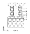
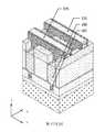
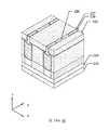
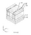
第1圖示出根據一些實施例之半導體電晶體元件100的透視圖。第2圖示出根據一些實施例之沿第1圖的X方向上之線A-A'截取的橫截面圖。第3圖至第5圖示出根據一些實施例之第1圖的第一源極/汲極區域、閘極區域及第二源極/汲極區域中分別沿Y方向上的線B-B'、C-C'及D-D'所截取之橫截面圖。或者,第2圖至第5圖以及後文中其他橫截面圖亦可單獨展示各種實施例。又,出於說明目的,將一些部件移除,示為透明的,或僅以邊界線示出。又,相關於一個圖所論述之特徵可在另一圖中省去,但可在適當時併入彼圖中所示實施例中。第2圖示出可整合在一個基板中之在左邊的短通道電晶體元件及在右邊的長通道電晶體元件。除非另有陳述,否則除了元件尺寸以外,短通道電晶體元件及長通道電晶體元件之特徵可為類似的。FIG. 1 shows a perspective view of a
如第1圖、第2圖及第5圖中所示,半導體電晶體元件100包括通道結構102及包覆通道結構102之閘極結構104。通道結構102可包括由閘極結構104之金屬部件的堆疊分離並圍繞之半導體層的堆疊。第一源極/汲極磊晶結構106及第二源極/汲極磊晶結構108設置在通道結構102之相對端部上。作為實例,通道結構102可為不摻雜有p型及n型雜質之純矽層。通道結構102之厚度可在約3 nm與約15 nm之間的範圍中。通道結構102之寬度可在約6 nm與約40 nm之間的範圍中。作為實例,閘極結構104可包括閘極介電材料(諸如,高介電常數材料(介電常數大於7))、功函數金屬材料,及填充金屬材料(諸如,鎢或鋁)。閘極結構104之厚度可在約2 nm與約10 nm之間的範圍中。在一些實施例中,第一及第二源極/汲極磊晶結構106、108包括半導體材料,諸如,矽、鍺或矽鍺。第一及第二源極/汲極磊晶結構106、108可為六邊形或類鑽石形狀。第一及第二源極/汲極磊晶結構106、108可分別為半導體電晶體元件100之源極區域及汲極區域。As shown in FIGS. 1 , 2 and 5 , the
如第2圖中所示,在半導體電晶體元件100之前側上,前側互連結構114可設置在閘極結構104以及第一及第二源極/汲極磊晶結構106、108之上。前側互連結構114可包括設置在前側層間介電層112內並由前側層間介電層112圍繞之複數個前側金屬層116。前側金屬層116包括垂直互連件(諸如,通孔或接觸件),及水平互連件(諸如,金屬接線)。前側互連結構114電連接半導體電晶體元件之各種特徵或結構。舉例而言,閘極接觸件110可設置在閘極結構104上並經由前側金屬層116連接至外部電路。As shown in FIG. 2 , on the front side of the
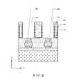
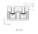
在半導體電晶體元件100之背側上,在一些實施例中,背側源極/汲極接觸件120被設置成下伏於第一源極/汲極磊晶結構106並將第一源極/汲極磊晶結構106連接至背側電力導軌122,此背側電力導軌122設置在背側源極/汲極接觸件120之下。背側互連結構124可形成為電耦接至背側源極/汲極接觸件120。背側互連結構124可包括設置在背側層間介電層212內並由背側層間介電層212圍繞之複數個背側金屬接線216及金屬通孔218。背側互連結構124電連接半導體電晶體元件之各種特徵或結構。舉例而言,背側互連結構124可包括將外部電路連接至背側源極/汲極接觸件120之背側電力導軌122。舉例而言,背側源極/汲極接觸件120及背側電力導軌122可包括金屬材料。舉例而言,背側源極/汲極接觸件120可包括金屬,諸如,鎢(W)、鈷(Co)、釕(Ru)、鋁(Al)、銅(Cu)或其他適當材料。作為實例,背側源極/汲極接觸件120可具有約5 nm至約50 nm之間的厚度及約20 nm至約40 nm之間的寬度。因此,第一源極/汲極磊晶結構106可自半導體電晶體元件100之背側經由背側源極/汲極接觸件120連接至外部電路。藉此,提供了更多的金屬佈線靈活性,且可減小單元電容。在一些實施例中,第一介電內襯118是沿背側源極/汲極接觸件120之側壁設置。作為實例,第一介電內襯118可具有小於約5 nm之厚度。On the backside of the
如第1圖至第3圖中所示,背側源極/汲極接觸件120可位在第一源極/汲極磊晶結構106之凹陷底表面106b上。在一些實施例中,第一源極/汲極磊晶結構106之底表面106b可凹陷成凸形達到垂直地比閘極結構104之底表面104b深的位置。在一些實施例中,第一源極/汲極磊晶結構106之底表面106b可如第2圖中所示沿X方向自第一源極/汲極磊晶結構106至第二源極/汲極磊晶結構108具有凸形,且亦如第3圖中所示沿Y方向具有凸形。Y方向可垂直於X方向。在一些實施例中,第一源極/汲極磊晶結構106之底表面106b可垂直地比閘極結構104之底表面104b高約5 nm至深約20 nm。在一些實施例中,低溫磊晶層119可設置在第一源極/汲極磊晶結構106之凹陷底表面106b與背側源極/汲極接觸件120之間,且金屬合金層121可設置在低溫磊晶層119上。低溫磊晶層119可具有比第一源極/汲極磊晶結構106之摻雜濃度大的摻雜濃度,使得隨後可形成較佳的金屬合金層121以獲得效能。作為實例,低溫磊晶層119可具有小於約20 nm之厚度。金屬合金層121可形成在第一源極/汲極磊晶結構106上以用於接觸件著陸。金屬合金層121可為藉由自對準矽化物製程形成之矽化物層。金屬合金層121可包括選自矽化鈦、矽化鈷、矽化鎳、矽化鉑、鎳鉑矽化物、矽化鉺、矽化鈀、其組合或其他適當材料之材料。在一些實施例中,金屬合金層121可包括鍺。As shown in FIGS. 1-3 , the backside source/
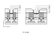
如第1圖、第2圖及第4圖中所示,第二源極/汲極磊晶結構108之底表面108b可凹陷至垂直地與閘極結構104之底表面104b相等或甚至更深的位置。第二源極/汲極磊晶結構108之底表面108b可甚至更深地凹陷至垂直地超過通道結構102之底表面102b的位置。在一些實施例中,第二源極/汲極磊晶結構108之底表面108b可如第2圖中所示沿X方向自第一源極/汲極磊晶結構106至第二源極/汲極磊晶結構108具有凸形,且亦如第4圖中所示沿Y方向具有凸形。Y方向可垂直於X方向。在一些實施例中,第二源極/汲極磊晶結構108之底表面108b可垂直地比閘極結構104之底表面104b高約15 nm至深約30 nm。第二源極/汲極磊晶結構108之凹陷底表面108b在短通道電晶體元件中可比在長通道電晶體元件中更低。底表面108b可在長通道電晶體元件中比在短通道電晶體元件中凹陷至更淺的位置。與其中第二源極/汲極磊晶結構108之底表面108b在通道結構102的最底部下方之實施例相比較而言,進一步減小單元電容。As shown in FIGS. 1, 2 and 4, the
如第1圖至第2圖及第4圖至第5圖中所示,在半導體電晶體元件100之背側上,在一些實施例中,背側介電帽126設置在閘極結構104之下。背側介電帽126亦可在第二源極/汲極磊晶結構108之下延伸。背側介電帽126可被下部隔離結構160圍繞。背側介電帽126替換原始的半導體主體材料,幫助分離閘極結構104與背側源極/汲極接觸件120並使閘極結構104與背側源極/汲極接觸件120絕緣,且從而減小單元電容並消除電流洩漏主題,諸如,閘極結構104與背側源極/汲極接觸件120之間的洩漏。背側介電帽126可包括氧化物、氮化物、碳氮化物或低介電常數的介電材料。在一些實施例中,第二介電內襯127襯在背側介電帽126之內側壁上。第二介電內襯127保護第二源極/汲極磊晶結構108免於氧化,且亦在製造製程期間防止金屬閘極閾值偏移。第二介電內襯127可包括介電材料。As shown in FIGS. 1-2 and 4-5, on the backside of the
如第1圖至第2圖中所示,在一些實施例中,背側源極/汲極接觸件120可包括直接在閘極結構104下方延伸之凸緣236。背側源極/汲極接觸件120可接觸第二介電內襯127或在第二介電內襯127被省去時接觸背側介電帽126。在一些實施例中,凸緣236可為如上所述或如以下與第23圖至第32B圖相關聯地描述之保護性間隔物的形成與移除之結果。作為實例,凸緣236可具有小於5 nm之寬度及小於20 nm之高度。又,內部間隔物128可設置在閘極結構104之金屬部件的相對端部上,以隔離閘極結構104與第一及第二源極/汲極磊晶結構106、108。凸緣236亦可接觸內部間隔物128及/或閘極結構104。在一些實施例中,閘極間隔物134是沿閘極結構104之上部部分的相對側壁設置。內部間隔物128之外表面可與通道結構102及/或閘極間隔物134之外表面實質上共面。在一些實施例中,上部隔離結構220設置在閘極間隔物134之間的溝槽中。上部隔離結構220提供閘極結構104之間的電絕緣。As shown in FIGS. 1-2 , in some embodiments, the backside source/
如第5圖中所示,在一些實施例中,閘極結構104包括閘極介電層232及閘電極230。閘電極230包括一或更多個功函數金屬層及填充金屬。閘極介電層232可保形地形成為內襯閘電極230之外表面。閘極介電層232可與下部隔離結構160及通道結構102接觸。在一些實施例中,閘極介電層232包括高介電常數的材料(介電常數大於7),諸如,氧化鉿(HfO2)、氧化鋯(ZrO2)、氧化鑭(La2O3)、鉿鋁氧化物(HfAlO2)、鉿矽氧化物(HfSiO2)、氧化鋁(Al2O3)或其他適當材料。As shown in FIG. 5 , in some embodiments, the
如第1圖及第3圖至第5圖中所示,在一些實施例中,下部隔離結構160、中間隔離結構132及硬遮罩136可共同地用作絕緣結構,此絕緣結構沿Y方向將兩個半導體電晶體元件100a、100b分離開。在一些實施例中,氣隙192可形成為圍繞第一源極/汲極磊晶結構106及第二源極/汲極磊晶結構108之下部部分。As shown in FIGS. 1 and 3 to 5 , in some embodiments, the
第6圖至第33B圖繪示根據本揭示案之一些實施例的處於各種階段之用於製造半導體電晶體元件的方法。在一些實施例中,第6圖至第33B圖中所示之半導體電晶體元件可為在積體電路(IC)的處理期間製造之中間元件,或其一部分,此些中間元件可包括靜態隨機存取記憶體(SRAM)、邏輯電路、被動部件(諸如,電阻器、電容器及電感器),及/或主動部件,諸如,p型場效應電晶體(PFET)、n型FET(NFET)、多閘極FET、金屬-氧化物半導體場效應電晶體(MOSFET)、互補金屬-氧化物半導體(CMOS)電晶體、雙極電晶體、高電壓電晶體、高頻率電晶體、其他記憶體單元,及其組合。FIGS. 6-33B illustrate a method for fabricating a semiconductor transistor device at various stages in accordance with some embodiments of the present disclosure. In some embodiments, the semiconductor transistor elements shown in FIGS. 6-33B may be intermediate elements, or portions thereof, fabricated during processing of integrated circuits (ICs), such intermediate elements may include static random access memory (SRAM), logic circuits, passive components such as resistors, capacitors, and inductors, and/or active components such as p-type field effect transistors (PFETs), n-type FETs (NFETs), Multi-gate FETs, Metal-Oxide Semiconductor Field-Effect Transistors (MOSFETs), Complementary Metal-Oxide Semiconductor (CMOS) transistors, Bipolar Transistors, High Voltage Transistors, High Frequency Transistors, Other Memory Cells, and its combinations.
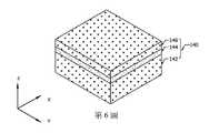
如第6圖之透視圖中所示,提供基板140。在一些實施例中,基板140可為晶圓的一部分,且可包括矽(S)、鍺(Ge)、矽鍺(SiGe)、砷化鎵(GaAs)或其他適當半導體材料。在一些實施例中,基板140為絕緣層上矽晶(semiconductor-on-insulator,SOI)結構,其包括塊體半導體142、在塊體半導體142上之絕緣體基板層144,及在絕緣體基板層144上之半導體基板層146。在各種實施例中,基板140可包括多種基板結構及材料中之任一者。As shown in the perspective view of FIG. 6, a
如第7圖之透視圖中所示,在一些實施例中,在基板140之上形成蝕刻終止層148,且在蝕刻終止層148之上形成堆疊結構150。蝕刻終止層148可充當用於如第22A圖中所示之後續基板移除製程的蝕刻終止層。蝕刻終止層148是由具有與半導體基板層146不同的蝕刻速率之材料製成,且可由Si、Si化合物、SiGe、Ge或Ge化合物製成。堆疊結構150包括交替堆疊之第一半導體層152及第二半導體層154。第一半導體層152將充當半導體電晶體元件之通道區域。第二半導體層154為犧牲層,其將隨後被移除並被閘極材料替換。第一半導體層152及第二半導體層154由具有不同晶格常數之材料製成,且可包括一或更多層的Si、Ge、SiGe、GaAs、InSb、GaP、GaSb、InAlAs、InGaAs、GaSbP、GaAsSb或InP。在一些實施例中,第一半導體層152及第二半導體層154由Si、Si化合物、SiGe、Ge或Ge化合物製成。堆疊結構150可經由磊晶形成在基板140上,使得堆疊結構150形成結晶層。儘管第7圖示出了第一半導體層152之四個層及第二半導體層154之三個層,但層的數目並不限於此,且對於每一種層而言層的數目可小至1。在一些實施例中,形成第一及第二半導體層中每一者的2至10個層。藉由調整堆疊之層的數目,可調整半導體電晶體元件之驅動電流。As shown in the perspective view of FIG. 7 , in some embodiments, an
在一些實施例中,第一半導體層152可為不含鍺之純矽層。第一半導體層152亦可為實質上純的矽層,例如,具有低於約百分之一之鍺原子百分比。另外,第一半導體層152可為本徵(intrinsic)的,其不摻雜有p型及n型雜質。在一些實施例中,第一半導體層152之厚度在約3 nm與約15 nm之間的範圍中。In some embodiments, the
在一些實施例中,第二半導體層154可為具有大於零的鍺原子百分比之SiGe層。在一些實施例中,第二半導體層154之鍺百分比在約百分之十與約百分之五十之間的範圍中。在一些實施例中,第二半導體層154之厚度在約2 nm與約10 nm之間的範圍中。In some embodiments, the
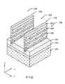
如第8圖之透視圖中所示,在一些實施例中,堆疊結構150(參見第7圖)經圖案化而形成在X方向上延伸之鰭片結構156及溝槽158。在一些實施例中,堆疊結構150是藉由使用圖案化的遮罩層157作為蝕刻遮罩之蝕刻製程圖案化,使得移除堆疊結構150之未被遮罩層157覆蓋的部分。亦可在此製程中部分地或全部地移除未被遮罩層157覆蓋之半導體基板層146及蝕刻終止層148。遮罩層157可包括第一遮罩層及第二遮罩層。第一遮罩層可為由氧化矽製成之襯墊氧化物層,其可藉由熱氧化製程形成。第二遮罩層可由氮化矽(SiN)製成,其是藉由包括低壓CVD(LPCVD)及電漿增強CVD(PECVD)之化學氣相沉積(CVD)、物理氣相沉積(PVD)、原子層沉積(ALD)或其他適當製程形成。可使用各種多重圖案化技術來圖案化遮罩層157,諸如,自對準雙重圖案化(self-aligned double patterning, SADP)、自對準四重圖案化(self-aligned quadruple patterning, SAQP),及其類似者。第8圖示出在Y方向上佈置且彼此平行之兩個鰭片結構156,但鰭片結構之數目並不限於此,且可小至一個以及三個或三個以上。在一些實施例中,在鰭片結構156之兩側上形成一或更多個虛設鰭片結構,以改良圖案化操作中之圖案保真度。As shown in the perspective view of FIG. 8, in some embodiments, the stack structure 150 (see FIG. 7) is patterned to form
如第9圖之透視圖中所示,在一些實施例中,下部隔離結構160形成於在溝槽158之下部部分中的絕緣體基板層144之上,其亦稱作淺溝槽隔離(STI)結構。鰭片結構156之上部部分自下部隔離結構160暴露。可藉由在絕緣體基板層144之上形成絕緣材料、之後進行平坦化操作來形成下部隔離結構160。絕緣材料接著凹陷以形成下部隔離結構160,使得暴露鰭片結構156之上部部分。絕緣材料可包括介電材料,諸如,氮化物(例如,氮化矽、氧氮化矽、氧碳氮化矽、碳氮化矽)、碳化物(例如,碳化矽、氧碳化矽)、氧化物(例如,氧化矽)、硼矽酸鹽玻璃、磷矽酸鹽玻璃、硼磷矽酸鹽玻璃、具有小於7的介電常數之低介電常數介電材料(例如,碳摻雜氧化物、SiCOH),或其類似者。在一些實施例中,下部隔離結構160是經由各種步驟形成的,包括熱氧化或沉積製程(例如,物理氣相沉積(PVD)、化學氣相沉積(CVD)、電漿增強化學氣相沉積(PECVD)、原子層沉積(ALD)、濺射,等),及移除製程(例如,濕式蝕刻、乾式蝕刻、化學機械平坦化,等)。As shown in the perspective view of FIG. 9, in some embodiments,
如第10圖之透視圖中所示,在一些實施例中,在鰭片結構156之外表面之上形成包覆半導體層161。在一些實施例中,包覆半導體層161包括半導體材料,諸如,鍺、矽鍺,或其類似者。在一些實施例中,包覆半導體層161包括與第二半導體層154(見第9圖)相同之材料。另外,在一些實施例中,可藉由磊晶生長製程或沉積製程(例如,PVD、CVD、PECVD、ALD、濺射,等)形成包覆半導體層161。As shown in the perspective view of FIG. 10 , in some embodiments, a
如第11圖之透視圖中所示,在一些實施例中,在鰭片結構156之間的下部隔離結構160之上形成中間隔離結構132。可沿包覆半導體層161及下部隔離結構160之側壁在中間隔離結構132與下部隔離結構160之間形成介電內襯130。可接著在中間隔離結構132及介電內襯130之頂部上形成硬遮罩136。中間隔離結構132及介電內襯130提供鰭片結構156之間的電絕緣,且硬遮罩136防止在未來圖案化步驟期間損失中間隔離結構132。As shown in the perspective view of FIG. 11 , in some embodiments,
在一些實施例中,藉由沉積(例如,PVD、CVD、PECVD、ALD、濺射,等)及移除(例如,蝕刻、化學機械平坦化,等)製程形成介電內襯130、中間隔離結構132及硬遮罩136。中間隔離結構132可具有在鰭片結構156之頂表面下方的頂表面。在第11圖中未示出之一些實施例中,硬遮罩136之平坦化製程亦可自鰭片結構156上方移除包覆半導體層161。硬遮罩136可具有與鰭片結構156之頂表面共面的頂表面。在一些實施例中,中間隔離結構132及下部隔離結構160可各自包括低介電常數介電材料(其中介電常數小於7),諸如,氧氮化矽、碳氮化矽、氧碳化矽、氧碳氮化矽、氮化矽,或一些其他適當的低介電材介電材料。介電內襯130可包括與中間隔離結構132不同之材料,以用於選擇性移除製程。硬遮罩136可包括高介電常數介電材料,其中介電常數大於7,諸如,氧化鉿、氧化鋯、鉿鋁氧化物、鉿矽氧化物、氧化鋁,或一些其他適當的高介電常數介電材料。In some embodiments, the
如第12圖之透視圖中所示,在一些實施例中,自鰭片結構156之頂部蝕刻包覆半導體層161及遮罩層157(見第9圖)。可自移除製程暴露第一半導體層152及包覆半導體層161之頂表面。在一些實施例中,例如,藉由乾式蝕刻製程及/或濕式蝕刻製程選擇性地蝕刻硬遮罩層136。As shown in the perspective view of FIG. 12, in some embodiments, the
如第13圖之透視圖中所示,在一些實施例中,在鰭片結構156之上沿Y方向、在X方向上彼此間隔開地形成虛設閘極結構170。在一些實施例中,虛設閘極結構170可包括犧牲閘極介電層162、犧牲閘電極層164、襯墊層166及遮罩層168,其以所述次序一個堆疊在另一個之上。儘管第13圖中示出兩個虛設閘極結構170,但虛設閘極結構170之數目並不限於此,且可多於或少於兩個。在一些實施例中,犧牲閘極介電層162可包括(例如)介電材料,諸如,氮化物(例如,氮化矽、氧氮化矽)、碳化物(例如,碳化矽)、氧化物(例如,氧化矽),或一些其他適當材料。犧牲閘電極層164可包括(例如)多晶矽。襯墊層166及遮罩層168可包括熱氧化物、氮化物及/或其他硬遮罩材料並藉助於光微影製程來形成。As shown in the perspective view of FIG. 13, in some embodiments,
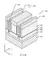
隨後,可沿虛設閘極結構170之相對側壁形成閘極間隔物134。舉例而言,藉由使用電漿增強化學氣相沉積(PECVD)、低壓化學氣相沉積(LPCVD)、次大氣壓化學氣相沉積(sub-atmospheric chemical vapor deposition, SACVD)或其類似者保形地形成用於側壁間隔物之絕緣材料的毯覆層以覆蓋虛設閘極結構170。以保形方式來沉積毯覆層,以使得毯覆層形成為在虛設閘極結構170的垂直表面(諸如,側壁)、水平表面及頂部上具有實質上相等之厚度。在一些實施例中,毯覆層之絕緣材料可包括基於氮化矽之材料。接著使用非等向性製程蝕刻毯覆層,以在虛設閘極結構170之相對側壁上形成閘極間隔物134。Subsequently,
如第14A圖之透視圖、第14B圖之X方向橫截面圖、第14C圖之閘極區域中的Y方向橫截面圖及第14D圖之源極區域或汲極區域中的Y方向橫截面圖中所示,在一些實施例中,執行移除製程以根據虛設閘極結構170自第一源極/汲極區域176及第二源極/汲極區域178移除鰭片結構156。因此,第一半導體層152及第二半導體層154沿X方向縮短,且可垂直地與閘極間隔物134(參見第14B圖)對準。作為實例,藉由使用應變源極/汲極(strained source/drain, SSD)蝕刻製程移除鰭片結構156之已暴露部分。可以多種方式來執行SSD蝕刻製程。在一些實施例中,可藉由用電漿源及反應氣體之乾式化學蝕刻來執行SSD蝕刻製程。電漿源可為電感耦合電漿(inductively coupled plasma, ICR)蝕刻、變壓器耦合電漿(transformer coupled plasma, TCP)蝕刻、電子迴旋共振(electron cyclotron resonance, ECR)蝕刻、反應性離子蝕刻(reactive ion etch, RIE),或其類似者,且反應氣體可為氟基氣體、氯氣(Cl2)、溴化氫(HBr)、氧氣(O2)、其類似者,或其組合。在一些其他實施例中,可藉由濕式化學蝕刻執行SSD蝕刻製程,諸如,過氧化銨混合物(APM)、氫氧化銨(NH4OH)、四甲基氫氧化銨(TMAH)、其組合,或其類似者。在又一些其他實施例中,可藉由乾式化學蝕刻與濕式化學蝕刻之組合來執行SSD蝕刻步驟。另外,在一些實施例中,移除製程可部分地或完全地移除虛設閘極結構170之間的最底部第一半導體層152。最底部第一半導體層152可在第一源極/汲極區域176及第二源極/汲極區域178(參見第14B圖)中沿X方向具有凹入頂表面。在一些實施例中,最底部第一半導體層152之頂表面可在下部隔離結構160之間凹陷,並低於下部隔離結構160之頂表面。As shown in the perspective view of Fig. 14A, the X-direction cross-sectional view of Fig. 14B, the Y-direction cross-sectional view of the gate region of Fig. 14C, and the Y-direction cross-section of the source region or the drain region of Fig. 14D As shown, in some embodiments, a removal process is performed to remove the
另外,移除製程亦可包括等向性蝕刻劑,以進一步移除第二半導體層154之在閘極間隔物134及/或虛設閘極結構170之下的末端部分。因此,在移除製程之後,第一半導體層152在X方向上比第二半導體層154寬。在移除製程之後,第一半導體層152可形成為電晶體元件之通道結構。將瞭解,通道結構可表現出如第14B圖之橫截面圖及其他諸圖中所繪示之堆疊的類矩形形狀,而在其他實施例中,通道結構可表現出其他形狀,諸如,圓形、八邊形、橢圓形、菱形,或其類似者。Additionally, the removal process may also include an isotropic etchant to further remove end portions of the
如第15A圖之透視圖及第15B圖之X方向橫截面圖中所示,在一些實施例中,內部間隔物128在X方向上形成在第二半導體層154之端部上。內部間隔物128之外表面可與第一半導體層152及/或閘極間隔物134之外表面實質上共面。在一些實施例,藉由沉積製程(例如,CVD、PVD、PECVD、ALD、濺射,等)、之後進行選擇性移除製程來形成內部間隔物128。舉例而言,在一些實施例中,可首先沿側壁及在虛設閘極結構170之上形成連續層。接著,可進行垂直蝕刻製程,以移除連續層之未被閘極間隔物134垂直覆蓋的部分,以形成內部間隔物128。另外,在一些實施例中,內部間隔物128包括介電材料,諸如,氧氮化矽、碳氮化矽、氧碳化矽、氧碳氮化矽、氮化矽或一些其他適當材料。As shown in the perspective view of FIG. 15A and the X-direction cross-sectional view of FIG. 15B, in some embodiments,
如第16A圖之透視圖、第16B圖之X方向橫截面圖及第16C圖之第一源極/汲極區域中的Y方向橫截面圖中所示,在一些實施例中,犧牲源極/汲極接觸件180形成在第一源極/汲極區域176之下,其中硬遮罩層182覆蓋第二源極/汲極區域178。在一些實施例中,犧牲源極/汲極接觸件180形成為穿過蝕刻終止層148並在半導體基板層146中延伸至深處。作為實例,犧牲源極/汲極接觸件180可具有約50 nm之厚度。在一些實施例中,首先藉由蝕刻最底部第一半導體層152、蝕刻終止層148及/或半導體基板層146之直接在第一源極/汲極區域176之下的至少一部分而形成溝槽。接著,在溝槽中填充犧牲材料以形成犧牲源極/汲極接觸件180。在一些實施例中,犧牲源極/汲極接觸件180可包括具有大於零之鍺原子百分比的本徵SiGe材料。在一些實施例中,犧牲源極/汲極接觸件180之鍺百分比在約百分之十與約百分之五十之間的範圍中。在一些實施例中,犧牲源極/汲極接觸件180包括與第二半導體層154相同之材料。另外,在一些實施例中,可藉由磊晶生長製程或沉積製程(例如,PVD、CVD、PECVD、ALD、濺射,等)形成犧牲源極/汲極接觸件180。藉由形成溝槽及在溝槽中之犧牲源極/汲極接觸件180,可稍後藉由替換犧牲源極/汲極接觸件180而使源極/汲極接觸件形成為自對準的,以使得消除了接觸件著陸之疊加偏移。As shown in the perspective view of Figure 16A, the X-direction cross-sectional view of Figure 16B, and the Y-direction cross-sectional view in the first source/drain region of Figure 16C, in some embodiments, the sacrificial source The /
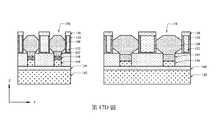
如第17A圖之透視圖、第17B圖之X方向橫截面圖、第17C圖之第一源極/汲極區域中的Y方向橫截面圖及第17D圖之第二源極/汲極區域中的Y方向橫截面圖中所示,在一些實施例中,第一源極/汲極磊晶結構106及第二源極/汲極磊晶結構108分別形成在虛設閘極結構170之相對側上的第一源極/汲極區域176及第二源極/汲極區域178中。在一些實施例中,第一源極/汲極磊晶結構106可形成在犧牲源極/汲極接觸件180上。第二源極/汲極磊晶結構108可形成在最底部第一半導體層152或半導體基板層146上。第一及第二源極/汲極磊晶結構106、108可分別為半導體電晶體元件之源極及汲極。在一些實施例中,第一及第二源極/汲極磊晶結構106、108包括半導體材料。舉例而言,第一及第二源極/汲極磊晶結構106、108可包括摻雜矽、鍺,或諸如硼摻雜矽鍺(SiGeB)之矽鍺。在一些實施例中,第一及第二源極/汲極磊晶結構106、108是藉助於磊晶生長製程形成。第一源極/汲極磊晶結構106及第二源極/汲極磊晶結構108可為六邊形或類鑽石形狀。氣隙192可形成為圍繞第一源極/汲極磊晶結構106及第二源極/汲極磊晶結構108之下部部分。在一些實施例中,在形成第一及第二源極/汲極磊晶結構106、108之前,在第一及第二源極/汲極磊晶結構106、108下面形成中間源極/汲極層107。中間源極/汲極層107可包括硼摻雜矽鍺(SiGeB)。作為實例,中間源極/汲極層107可具有約20 nm之厚度。As shown in the perspective view of Fig. 17A, the X-direction cross-sectional view of Fig. 17B, the Y-direction cross-sectional view of the first source/drain region of Fig. 17C, and the second source/drain region of Fig. 17D As shown in the cross-sectional view in the Y direction, in some embodiments, the first source/
在一些實施例中,磊晶生長層之深度受加載效應影響。具有較大尺寸之元件可形成有比具有較小尺寸之元件厚的磊晶層。第17B圖至第17D圖及後文中一些圖示出在左邊的短通道電晶體及在右邊的長通道電晶體,以並排地繪示出此主題。如第17B圖至第17D圖中所示,中間源極/汲極層107及第一及第二源極/汲極磊晶結構106、108在長通道電晶體中比在短通道電晶體中形成得更深。在一些實施例中,在長通道電晶體中,中間源極/汲極層107形成為其底表面超過在第一源極/汲極區域176及第二源極/汲極區域178之下的蝕刻終止層148。在一些實施例中,在長通道電晶體中,第一及第二源極/汲極磊晶結構106、108形成為底表面之邊緣超過閘極結構104之底表面104b。舉例而言,中間源極/汲極層107及第一及第二源極/汲極磊晶結構106、108在長通道電晶體中可比在短通道電晶體中深約5 nm至10 nm。因此,第一及第二源極/汲極磊晶結構106、108之底部部分接觸最底部第一半導體層152。將在後續製程(例如,參見第28A圖至第28D圖)期間移除最底部第一半導體層152,且因此第一及第二源極/汲極磊晶結構106、108之底部部分可能暴露於非所要之蝕刻製程且可能損壞並形成會影響長通道電晶體的效能或甚至使長通道電晶體失效之凹坑。因此,以下與第22A圖至第28D圖相關聯地繪示出形成保護性間隔物以保護長通道電晶體免受此損壞的方法之一些實施例。In some embodiments, the depth of the epitaxial growth layer is affected by the loading effect. Devices with larger dimensions can be formed with thicker epitaxial layers than devices with smaller dimensions. Figures 17B-17D and some of the following figures show a short channel transistor on the left and a long channel transistor on the right to depict this subject side by side. As shown in FIGS. 17B to 17D, the intermediate source/
如第18A圖之透視圖、第18B圖之X方向橫截面圖、第18C圖之第一源極/汲極區域中的Y方向橫截面圖及第18D圖之第二源極/汲極區域中的Y方向橫截面圖中所示,在一些實施例中,在先前形成為覆蓋第一及第二源極/汲極磊晶結構106、108的結構之上形成上部隔離結構220。隨後執行平坦化製程,以降低閘極間隔物134並在同一水平面上暴露犧牲閘極介電層162及犧牲閘電極層164。在一些實施例中,蝕刻終止內襯210可保形地形成為內襯先前在形成上部隔離結構220之前形成的結構。在一些實施例中,蝕刻終止內襯210可包括氮化矽。在一些其他實施例中,蝕刻終止內襯210可包括其他介電材料,諸如,二氧化矽、氧氮化矽,或其類似者。可使用電漿增強CVD(PECVD)形成蝕刻終止內襯210,然而,亦可使用其他適當方法,諸如,低壓CVD(LPCVD)、原子層沉積(ALD)及其類似者。可藉由化學氣相沉積(CVD)、高密度電漿CVD、旋塗、濺射或其他適當方法形成上部隔離結構220。在一些實施例中,上部隔離結構220可包括二氧化矽。在一些其他實施例中,上部隔離結構220可包括其他介電材料,諸如,碳摻雜氧化物介電質(包括Si、O、C及/或H(SiCOH或SiOC))、低介電常數的材料,或有機材料(例如,聚合物)。平坦化操作可包括化學機械平坦化製程。As shown in the perspective view of Fig. 18A, the X-direction cross-sectional view of Fig. 18B, the Y-direction cross-sectional view of the first source/drain region of Fig. 18C, and the second source/drain region of Fig. 18D In some embodiments, an
如第19A圖之透視圖、第19B圖之X方向橫截面圖、第19C圖之閘極區域中的Y方向橫截面圖中所示,在一些實施例中,執行替換閘極製程以形成閘極結構104。在一些實施例中,藉由首先移除犧牲閘極介電層162及犧牲閘電極層164藉此暴露第一及第二半導體層152、154(參見第18B圖)而形成閘極結構104。上部隔離結構220在犧牲閘極介電層162及犧牲閘電極層164之移除期間保護第一及第二源極/汲極磊晶結構106、108。可使用電漿乾式蝕刻及/或濕式蝕刻來移除犧牲閘電極層164。當犧牲閘電極層164為多晶矽且上部隔離結構220為氧化矽時,可使用諸如TMAH溶液之濕式蝕刻劑來選擇性地移除犧牲閘電極層164。可使用電漿乾式蝕刻及/或濕式蝕刻來移除犧牲閘電極層164。隨後,亦移除犧牲閘極介電層162。如此,暴露第一及第二半導體層152、154。As shown in the perspective view of FIG. 19A, the X-direction cross-sectional view of FIG. 19B, and the Y-direction cross-sectional view in the gate region of FIG. 19C, in some embodiments, a replacement gate process is performed to form the
接著移除或使用蝕刻劑來蝕刻第二半導體層154及包覆半導體層161(參見第14C圖),此蝕刻劑可以比蝕刻第一半導體層152快的蝕刻速率選擇性地蝕刻第二半導體層154及包覆半導體層161。因為內部間隔物128是由對第二半導體層154及包覆半導體層161的材料具有蝕刻選擇性之材料製成,所以內部間隔物128保護第一及第二源極/汲極磊晶結構106、108免受用於蝕刻第二半導體層154及包覆半導體層161之蝕刻劑影響。The
接著在閘極間隔物134與內部間隔物128之間形成及/或填充閘極結構104。亦即,閘極結構104圍繞(或圍繞或包覆)第一半導體層152,其中將第一半導體層152稱作半導體電晶體元件之通道。閘極間隔物134設置在閘極結構104之相對側上。閘極結構104包括閘極介電層232及閘電極230。閘電極230包括一或更多個功函數金屬層及填充金屬。可保形地形成閘極介電層232。亦即,閘極介電層232與下部隔離結構160及第一半導體層152(參見第19C圖)接觸。在一些實施例中,閘極介電層232包括高介電常數材料(介電常數大於7),諸如,氧化鉿(HfO2)、氧化鋯(ZrO2)、氧化鑭(La2O3)、鉿鋁氧化物(HfAlO2)、鉿矽氧化物(HfSiO2)、氧化鋁(Al2O3)或其他適當材料。在一些實施例中,可藉由執行ALD製程或其他適當製程形成閘極介電層232。The
閘電極230之功函數金屬層形成在閘極介電層232上,且在一些實施例中功函數金屬層圍繞第一半導體層152。功函數金屬層可包括諸如氮化鈦(TiN)、氮化鉭(TaN)、鈦鋁矽化物(TiAlSi)、鈦矽氮化物(TiSiN)、鈦鋁(TiAl)、鉭鋁(TaAl)或其他適當材料之材料。在一些實施例中,可藉由執行ALD製程或其他適當製程形成功函數金屬層。閘電極230之填充金屬填充閘極間隔物134之間及內部間隔物128之間的剩餘空間。亦即,(若干)功函數金屬層與閘極介電層232及填充金屬接觸且在閘極介電層232與填充金屬之間。填充金屬可包括諸如鎢或鋁之材料。在沉積閘極介電層232及閘電極230之後,可接著執行平坦化製程(諸如,CMP製程),以移除閘極介電層232及閘電極230之過量部分以形成閘極結構104。The work function metal layer of the
在一些實施例中,在形成閘極結構104之前視情況形成界面層(未示出),以圍繞第一半導體層152之已暴露表面及半導體基板層146之已暴露表面(參見第19B圖、第19C圖)。在各種實施例中,界面層可包括介電材料(諸如,二氧化矽(SiO2)或氧氮化矽(SiON)),且可藉由化學氧化、熱氧化、原子層沉積(ALD)、化學氣相沉積(CVD)及/或其他適當方法而形成。In some embodiments, an interface layer (not shown) is optionally formed prior to forming the
如第20圖之透視圖中所示,在一些實施例中,在閘極結構104以及第一及第二源極/汲極磊晶結構106、108(參見第22B圖)之上形成前側互連結構114。前側互連結構114可包括設置在前側層間介電層112(參見第2圖)內並由前側層間介電層112圍繞之複數個前側金屬層116(參見第2圖)。前側互連結構114電連接半導體電晶體元件之各種特徵或結構(例如,閘極接觸件110及/或其他接觸件)。前側金屬層116包括垂直互連件(諸如,通孔或接觸件),及水平互連件(諸如,金屬接線)。各種互聯特徵可實施各種導電材料,包括銅、鎢及矽化物。在一些實施例中,使用鑲嵌製程形成銅多層互聯結構。隨後,在前側互連結構114之上形成載體基板240。舉例而言,載體基板240接合至前側互連結構114。在一些實施例中,載體基板240為藍寶石。在一些實施例中,載體基板240為矽、熱塑聚合物、氧化物、碳化物或其他適當材料。As shown in the perspective view of FIG. 20, in some embodiments, a front side interconnect is formed over the
如第21A圖之透視圖及第21B圖之X方向橫截面圖中所示,在一些實施例中,工件上下顛倒「翻轉」且自背側變薄。移除塊體基板142、絕緣體基板層144,以及半導體基板層146及下部隔離結構160之上部部分。犧牲源極/汲極接觸件180進一步被蝕刻成在半導體基板層146下方,且遮罩層242形成在犧牲源極/汲極接觸件180上及半導體基板層146之間。可使用(例如)CMP及/或TMAH蝕刻在複數個製程操作中移除塊體半導體142、絕緣體基板層144、半導體基板層146及下部隔離結構160。在一些實施例中,遮罩層242可由聚合物製成。或者,遮罩層242可由介電材料製成。As shown in the perspective view of Fig. 21A and the X-direction cross-sectional view of Fig. 21B, in some embodiments, the workpiece is "flipped" upside down and thinned from the back side. The
如第22A圖之透視圖及第22B圖之X方向橫截面圖中所示,在一些實施例中,移除半導體基板層146 (參見第21A圖),以在第二源極/汲極磊晶結構108及閘極結構104上方形成背側封蓋溝槽238。可藉由等向性蝕刻製程移除半導體基板層146,且蝕刻終止層148可充當此蝕刻製程之終止層。As shown in the perspective view of FIG. 22A and the X-direction cross-sectional view of FIG. 22B , in some embodiments, the semiconductor substrate layer 146 (see FIG. 21A ) is removed to allow the second source/drain epitaxy A
如第23圖之X方向橫截面圖中所示,在一些實施例中,移除蝕刻終止層148,以暴露最底部第一半導體層152。在一些實施例中,可自犧牲源極/汲極接觸件180之頂部移除遮罩層242 (參見第22B圖)。接著,沿犧牲源極/汲極接觸件180之頂部及/或側壁表面形成側壁層244。在一些實施例中,藉由介電材料(諸如,氧化鋁)之沉積製程、之後進行選擇性移除製程來形成側壁層244。舉例而言,側壁層244可具有約5 nm至6 nm之厚度。側壁層244覆蓋最底部第一半導體層152之靠近犧牲源極/汲極接觸件180及第一源極/汲極磊晶結構106的一部分,且因此保護第一源極/汲極磊晶結構106免於在最底部第一半導體層152之後續移除及第二源極/汲極磊晶結構108之凹陷(參見第26圖至第27圖)期間被損壞。第24圖至第25C圖示出形成保護性間隔物以保護第一源極/汲極磊晶結構106之替代實施例。第23圖之製造步驟自第26圖繼續。As shown in the X-direction cross-sectional view of FIG. 23 , in some embodiments, the
如第24圖之X方向橫截面圖中所示,在替代第23圖之一些實施例中,移除蝕刻終止層148(參見第22B圖),且部分地移除最底部第一半導體層152,而同時沿第一源極/汲極磊晶結構106、第二源極/汲極磊晶結構108及/或中間源極/汲極層107之上部側壁留下最底部第一半導體層152之拐角部分作為保護性間隔物246。在一些實施例中,藉由等向性濕式蝕刻製程部分地移除最底部第一半導體層152。蝕刻製程可暴露犧牲源極/汲極接觸件180之頂部及/或側壁表面。As shown in the X-direction cross-sectional view of FIG. 24, in some embodiments in lieu of FIG. 23, the etch stop layer 148 (see FIG. 22B) is removed, and the bottommost
如第25A圖之X方向橫截面圖、第25B圖之第一源極/汲極區域中的Y方向橫截面圖及第25C圖之第二源極/汲極區域中的Y方向橫截面圖中所示,在一些實施例中,沿犧牲源極/汲極接觸件180形成側壁內襯248。可藉由沿工件之已暴露表面沉積保形的介電內襯、之後進行非等向性蝕刻製程來形成側壁內襯248。舉例而言,側壁內襯248可具有約2 nm至3 nm之厚度。As shown in the X-direction cross-sectional view of FIG. 25A, the Y-direction cross-sectional view in the first source/drain region of FIG. 25B, and the Y-direction cross-sectional view of the second source/drain region of FIG. 25C As shown in, in some embodiments,
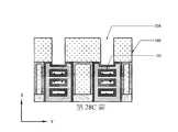
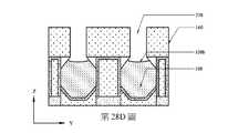
如第26圖、第27圖及第28B圖之X方向橫截面圖、第28A圖之透視圖、第28C圖之第二源極/汲極區域中的Y方向橫截面圖及第28D圖之閘極區域中的Y方向橫截面圖中所示,在一些實施例中,第二源極/汲極磊晶結構108自頂部凹陷。如第26圖中所示,首先移除中間源極/汲極層107。側壁層244及最底部第一半導體層152之下伏部分(如第23圖中所示)或側壁內襯248及保護性間隔物246(如第25A圖中所示)保護第一源極/汲極磊晶結構106免於在中間源極/汲極層107之移除期間被損壞。接著,如第27圖中所示,使第二源極/汲極磊晶結構108凹陷。接著,如第28B圖中所示,移除側壁層244(如第23圖中所示)或側壁內襯248(如第25A圖中所示)。當使第二源極/汲極磊晶結構108凹陷及移除側壁層244或側壁內襯248時,可部分地移除最底部第一半導體層152或保護性間隔物246,且最底部第一半導體層152或保護性間隔物246之拐角殘餘物152'可能仍沿第二源極/汲極磊晶結構108之上部側壁留下。在一些實施例中,藉由等向性蝕刻或等向性及非等向性蝕刻之組合使第二源極/汲極磊晶結構108凹陷。第二源極/汲極磊晶結構108之凹陷底表面108b在短通道電晶體元件中可比在長通道電晶體元件中更低。在短通道電晶體元件中,第二源極/汲極磊晶結構108之底表面108b可沿X方向達到垂直地比閘極結構104之底表面104b更深的位置(參見第28B圖)以及沿Y方向(參見第28D圖)凹陷成凸形(convex)。在一些實施例中,在短通道電晶體元件中,第二源極/汲極磊晶結構108之底表面108b垂直地比閘極結構104之底表面104b深約10 nm至20 nm。在長通道電晶體元件中,底表面108b可凹陷至垂直地等於閘極結構104之底表面104b或亦比閘極結構104之底表面104b更深的位置。As shown in Fig. 26, Fig. 27 and Fig. 28B, the X-direction cross-sectional view, the perspective view of Fig. 28A, the Y-direction cross-sectional view in the second source/drain region of Fig. 28C, and the 28D Fig. As shown in the Y-direction cross-sectional view in the gate region, in some embodiments, the second source/
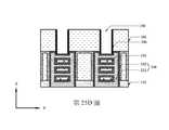
如第29A圖之透視圖、第29B圖之X方向橫截面圖、第29C圖之閘極區域中的Y方向橫截面圖及第29D圖之第二源極/汲極區域中的Y方向橫截面圖中所示,在一些實施例中,在背側封蓋溝槽238(參見第28A圖)中形成第二介電內襯127及背側介電帽126。第二介電內襯127及背側介電帽126可直接形成在第二源極/汲極磊晶結構108及閘極結構104(參見第28C圖)上方。第二介電內襯127保護第二源極/汲極磊晶結構108免於氧化,且亦在後續製造製程期間防止金屬閘極閾值偏移。可藉由(例如)保形沉積製程在背側封蓋溝槽238中沉積介電材料來形成第二介電內襯127,且可藉由(例如)沉積製程在第二介電內襯127上沉積介電材料、之後藉由CMP製程移除在背側封蓋溝槽238外部之過量介電材料來形成背側介電帽126。作為實例,第二介電內襯127可由諸如SiO2、Si3N4、碳氮化矽(SiCN)、氧碳化矽(SiOC)、氧碳氮化矽(SiOCN)及其類似者之低介電常數材料(k<7)或諸如HfO2、ZrO2、ZrAlOx、HfAlOx、HfSiOx、AlOx及其類似者之高介電常數材料(k>7)製成。在一些實施例中,背側介電帽126具有接觸第二源極/汲極磊晶結構108之凸起頂表面126s。作為實例,在CMP製程之後,背側介電帽126可形成有自底表面108b至背側介電帽126之頂表面的約40 nm之厚度。作為實例,第二介電內襯127可具有小於約5 nm之厚度。As shown in the perspective view of Fig. 29A, the X-direction cross-sectional view of Fig. 29B, the Y-direction cross-sectional view of the gate region of Fig. 29C, and the Y-direction transverse view of the second source/drain region of Fig. 29D As shown in the cross-sectional view, in some embodiments, the
如第30A圖之透視圖、第30B圖之X方向橫截面圖及第30C圖之第一源極/汲極區域中的Y方向橫截面圖中所示,在一些實施例中,移除犧牲源極/汲極接觸件180(參見第29B圖),且下伏的第一源極/汲極磊晶結構106自其背側凹陷以形成凹陷至第一源極/汲極磊晶結構106的上部部分中之背側源極/汲極接觸件溝槽234。可使用蝕刻劑使第一源極/汲極磊晶結構106凹陷或蝕刻第一源極/汲極磊晶結構106,此蝕刻劑可以比蝕刻周圍介電材料更快之蝕刻速率選擇性地蝕刻第一源極/汲極磊晶結構106。在一些實施例中,蝕刻製程為等向性的或包括等向性的蝕刻製程,且第一源極/汲極磊晶結構106之底表面106b可沿X方向(參見第30B圖)以及沿Y方向(參見第30C圖)凹陷成凸形達到垂直地比閘極結構104(參見第30B圖)之底表面104b更深的位置。在一些實施例中,第一源極/汲極磊晶結構106之底表面106b垂直地比閘極結構104之底表面104b深約10 nm至20 nm。在一些實施例中,當移除犧牲源極/汲極接觸件180及使第一源極/汲極磊晶結構106凹陷時,移除拐角殘餘物152'(參見第29B圖),在背側源極/汲極接觸件溝槽234中留下空的凸緣。As shown in the perspective view of Fig. 30A, the X-direction cross-sectional view of Fig. 30B, and the Y-direction cross-sectional view in the first source/drain region of Fig. 30C, in some embodiments, the sacrificial Source/drain contact 180 (see FIG. 29B ), and the underlying first source/
如第31A圖之透視圖、第31B圖之X方向橫截面圖及第31C圖之第一源極/汲極區域中的Y方向橫截面圖中所示,在一些實施例中,放大並鈍化背側源極/汲極接觸件溝槽234之開口,以用於在後續處理步驟中更佳地填充。可在放大的背側源極/汲極接觸件溝槽234中之第一源極/汲極磊晶結構106的凹陷底表面106b上形成低溫磊晶層119。低溫磊晶層119形成有比第一源極/汲極磊晶結構106之摻雜濃度大的摻雜濃度,使得隨後可形成較佳的金屬合金層以獲得效能。作為實例,低溫磊晶層119可形成有約5 nm之厚度。在一些實施例中,金屬合金層121可形成在低溫磊晶層119或第一源極/汲極磊晶結構106(若未形成低溫磊晶層119)上。金屬合金層121可為藉由自對準矽化物製程形成之矽化物層。金屬合金層121可包括選自矽化鈦、矽化鈷、矽化鎳、矽化鉑、鎳鉑矽化物、矽化鉺、矽化鈀、其組合或其他適當材料之材料。在一些實施例中,金屬合金層121可包括鍺。第一介電內襯118可沿背側源極/汲極接觸件溝槽234之側壁形成且可接觸第二介電內襯127。As shown in the perspective view of Fig. 31A, the X-direction cross-sectional view of Fig. 31B, and the Y-direction cross-sectional view in the first source/drain region of Fig. 31C, in some embodiments, the enlarged and passivated Openings of backside source/
如第32A圖之透視圖、第32B圖之X方向橫截面圖及第32C圖之第一源極/汲極區域中的Y方向橫截面圖中所示,在一些實施例中,在放大的背側源極/汲極接觸件溝槽234(參見第31B圖)中之低溫磊晶層119上形成背側源極/汲極接觸件120。在一些實施例中,背側源極/汲極接觸件120可形成有凸緣236,此凸緣236位於第29B圖之拐角殘餘物152'的位置處。背側源極/汲極接觸件120可具有接觸第一介電內襯118之內部側壁的側壁。在一些實施例中,背側源極/汲極接觸件120之凸緣236可直接上覆於內部間隔物128或閘極結構104延伸。在一些實施例中,背側源極/汲極接觸件120可由金屬製成,諸如,W、Co、Ru、Al、Cu或其他適當材料。作為實例,金屬合金層121可形成有約5 nm之厚度。在沉積背側源極/汲極接觸件120之後,可接著執行平坦化製程,諸如,化學機械平坦化製程。As shown in the perspective view of FIG. 32A, the X-direction cross-sectional view of FIG. 32B, and the Y-direction cross-sectional view in the first source/drain region of FIG. 32C, in some embodiments, the enlarged Backside source/
如第33A圖之透視圖及第33B圖之X方向橫截面圖中所示,在一些實施例中,形成背側電力導軌122及背側互連結構124以電耦接至背側源極/汲極接觸件120。背側互連結構124可包括設置在背側層間介電層212內並由背側層間介電層212圍繞之複數個背側金屬接線216及金屬通孔218。背側互連結構124電連接半導體電晶體元件之各種特徵或結構。舉例而言,背側互連結構124可設置在背側電力導軌122上並將外部電路連接至背側源極/汲極接觸件120。As shown in the perspective view of FIG. 33A and the X-direction cross-sectional view of FIG. 33B, in some embodiments, backside power rails 122 and
第34圖繪示形成具有多個電晶體元件之積體晶片的方法3400之一些實施例的流程圖,此些電晶體元件由於空氣間隔物結構及高介電常數的介電間隔物結構而具有高元件密度。34 illustrates a flow diagram of some embodiments of a
雖然以下將方法3400繪示並描述為一連串動作或事件,但將瞭解,不在限制意義上解釋此些動作或事件之所繪示排序。舉例而言,一些動作可以不同次序發生及/或與除了本文所繪示及/或描述之動作或事件以外的其他動作或事件同時發生。另外,實施本文中之描述的一或更多個態樣或實施例可能並不需要所有繪示動作。另外,本文中所描繪之動作中的一或更多者可在一或更多個單獨動作及/或階段中進行。Although
在動作3402處,在基板上形成堆疊的第一及第二半導體層之複數個鰭片結構。可在鰭片結構之間形成隔離結構。第6圖至第12圖繪示對應於動作3402之一些實施例的透視圖。At
在動作3404處,形成上覆於鰭片結構之複數個虛設閘極結構。第13圖繪示對應於動作3404之一些實施例的透視圖。At
在動作3406處,蝕刻鰭片結構之未被虛設閘極結構覆蓋的部分並自虛設閘極結構之相對側將其移除。第二半導體層可自第一半導體層水平凹陷,且內部間隔物可形成在第二半導體層之相對端部上。第14A圖至第15B圖繪示對應於動作3406之一些實施例的各種視圖。At act 3406, the portion of the fin structure not covered by the dummy gate structure is etched and removed from the opposite side of the dummy gate structure. The second semiconductor layer may be horizontally recessed from the first semiconductor layer, and internal spacers may be formed on opposite ends of the second semiconductor layer. FIGS. 14A-15B illustrate various views corresponding to some embodiments of act 3406 .
在動作3408處,在基板中形成第一虛設背側接觸件。第16A圖至第16C圖繪示對應於動作3408之一些實施例的各種視圖。At
在動作3410處,在凹陷的鰭片結構之相對側上形成第一及第二源極/汲極磊晶結構。第17A圖至第17D圖繪示對應於動作3410之一些實施例的各種視圖。At
在動作3412處,用金屬閘極結構替換第二半導體層。接著,形成閘極接觸件及前側互連結構。第18A圖至第20圖繪示對應於動作3412之一些實施例的各種視圖。At
在動作3414處,基板自背側變薄,且可在犧牲源極/汲極接觸件上形成遮罩層。第21A圖至第21B圖繪示對應於動作3414之一些實施例的各種視圖。At
在動作3416處,基板進一步薄化至低於犧牲源極/汲極接觸件之頂表面的位置,且在閘極結構及第二源極/汲極磊晶結構上方形成背側封蓋溝槽。可藉由在蝕刻終止層上終止之蝕刻製程使基板薄化。第22A圖至第22B圖繪示對應於動作3416之一些實施例的各種視圖。At
在動作3417處,移除蝕刻終止層以暴露最底部第一半導體層,且沿犧牲源極/汲極接觸件形成厚的側壁層。厚的側壁層覆蓋最底部第一半導體層之靠近犧牲源極/汲極接觸件及第一源極/汲極磊晶結構的一部分,且因此保護第一源極/汲極磊晶結構免於在最底部第一半導體層之後續移除及第二源極/汲極磊晶結構之凹陷期間被損壞。第23圖繪示對應於動作3417之一些實施例的橫截面圖。At
在動作3418及動作3420處,在替代動作3417之一些實施例中,在動作3418處在S/D磊晶結構之拐角處形成保護性間隔物,且在動作3420處沿犧牲源極/汲極接觸件形成側壁內襯。保護性間隔物及側壁內襯保護第一源極/汲極磊晶結構免於在最底部第一半導體層之後續移除及第二源極/汲極磊晶結構之凹陷期間被損壞。第24圖繪示對應於動作3418之一些實施例的橫截面圖。第25A圖至第25D圖繪示對應於動作3420之一些實施例的各種視圖。At
在動作3422處,在最底部第一半導體層之下部部分或保護性間隔物保護第一源極/汲極磊晶結構之側壁的情況下,使第二源極/汲極磊晶結構之底表面凹陷。第26圖至第28D圖繪示對應於動作3422之一些實施例的各種視圖。At
在動作3424處,在第二源極/汲極磊晶結構之底表面上形成背側介電帽。第29A圖至第29D圖繪示對應於動作3424之一些實施例的各種視圖。At
在動作3426處,形成接觸件溝槽,且使第一源極/汲極磊晶結構之底表面凹陷。第30A圖至第31C圖繪示對應於動作3426之一些實施例的各種視圖。At
在動作3428處,形成達到第一源極/汲極磊晶結構之底表面的背側源極/汲極接觸件。第32A圖至第32C圖繪示對應於動作3428之一些實施例的各種視圖。At
在動作3430處,形成背側電力導軌及背側互連結構。第33A圖至第33B圖繪示對應於動作3430之一些實施例的各種視圖。At
因此,在一些實施例中,本揭示案是關於一種形成半導體電晶體元件之方法。此方法包括在基板之上形成鰭片形通道結構,及在鰭片結構之相對端部上形成第一源極/汲極磊晶結構及第二源極/汲極磊晶結構。此方法進一步包括形成圍繞鰭片結構之金屬閘極結構。此方法進一步包括翻轉並部分地移除基板以形成背側封蓋溝槽,而同時沿第一源極/汲極磊晶結構及第二源極/汲極磊晶結構之上部側壁留下基板之下部部分作為保護性間隔物。此方法進一步包括在背側封蓋溝槽中形成背側介電帽。Accordingly, in some embodiments, the present disclosure is directed to a method of forming a semiconductor transistor device. The method includes forming a fin-shaped channel structure over a substrate, and forming a first source/drain epitaxial structure and a second source/drain epitaxial structure on opposite ends of the fin structure. The method further includes forming a metal gate structure surrounding the fin structure. The method further includes flipping and partially removing the substrate to form the backside capping trench while leaving the substrate along the upper sidewalls of the first source/drain epitaxial structure and the second source/drain epitaxial structure The lower part acts as a protective spacer. The method further includes forming a backside dielectric cap in the backside capping trench.
在其他實施例中,本揭示案是關於一種製造半導體電晶體元件之方法。此方法包括在基板之上形成鰭片形通道結構,及在鰭片形通道結構之一個側上在基板中形成犧牲源極/汲極接觸件。此方法進一步包括在鰭片結構之相對端部上形成第一源極/汲極磊晶結構及第二源極/汲極磊晶結構。第一源極/汲極磊晶結構上覆於犧牲源極/汲極接觸件。此方法進一步包括形成圍繞鰭片結構之金屬閘極結構以及翻轉並薄化基板。此方法進一步包括沿第一源極/汲極磊晶結構及第二源極/汲極磊晶結構之上部側壁形成保護性間隔物,及形成背側封蓋溝槽以暴露金屬閘極結構之底表面及第二源極/汲極磊晶結構之底表面。使第二源極/汲極磊晶結構之底表面凹陷。此方法進一步包括在背側封蓋溝槽中形成背側介電帽。In other embodiments, the present disclosure is directed to a method of fabricating a semiconductor transistor device. The method includes forming a fin-shaped channel structure over a substrate, and forming sacrificial source/drain contacts in the substrate on one side of the fin-shaped channel structure. The method further includes forming a first source/drain epitaxial structure and a second source/drain epitaxial structure on opposite ends of the fin structure. The first source/drain epitaxial structure overlies the sacrificial source/drain contacts. The method further includes forming a metal gate structure surrounding the fin structure and flipping and thinning the substrate. The method further includes forming protective spacers along upper sidewalls of the first source/drain epitaxial structure and the second source/drain epitaxial structure, and forming a backside capping trench to expose the metal gate structure the bottom surface and the bottom surface of the second source/drain epitaxial structure. The bottom surface of the second source/drain epitaxial structure is recessed. The method further includes forming a backside dielectric cap in the backside capping trench.
在另外實施例中,本揭示案是關於一種半導體元件。此半導體元件包括通道結構及包覆此通道結構之閘極結構。此半導體元件進一步包括設置在通道結構之相對端部上的第一源極/汲極磊晶結構及第二源極/汲極磊晶結構,及設置在第一源極/汲極磊晶結構之下且接觸第一源極/汲極磊晶結構的背側源極/汲極接觸件。此半導體元件進一步包括設置在閘極結構上之閘極接觸件,及設置在第一源極/汲極磊晶結構之下且接觸第一源極/汲極磊晶結構的背側源極/汲極接觸件。此半導體元件進一步包括背側介電帽,其設置在第二源極/汲極磊晶結構及閘極結構之下且沿第二源極/汲極磊晶結構及閘極結構延伸。第一源極/汲極磊晶結構具有具有凹形之底表面。In further embodiments, the present disclosure is directed to a semiconductor device. The semiconductor device includes a channel structure and a gate structure covering the channel structure. The semiconductor device further includes a first source/drain epitaxial structure and a second source/drain epitaxial structure disposed on opposite ends of the channel structure, and a first source/drain epitaxial structure disposed on the first source/drain epitaxial structure under and in contact with the backside source/drain contact of the first source/drain epitaxial structure. The semiconductor device further includes a gate contact disposed on the gate structure, and a backside source/source electrode disposed under the first source/drain epitaxial structure and contacting the first source/drain epitaxial structure Drain contacts. The semiconductor device further includes a backside dielectric cap disposed under the second source/drain epitaxial structure and the gate structure and extending along the second source/drain epitaxial structure and the gate structure. The first source/drain epitaxial structure has a bottom surface having a concave shape.
前文概述了若干實施例之特徵,使得熟習此項技術者可較佳地理解本揭示案之態樣。熟習此項技術者應瞭解,他們可容易地使用本揭示案作為設計或修改用於實現相同目的及/或達成本文中所介紹之實施例之相同優勢的其他製程及結構的基礎。熟習此項技術者亦應認識到,此些等效構造不脫離本揭示案之精神及範疇,且他們可在不脫離本揭示案之精神及範疇的情況下在本文作出各種改變、代替及替換。The foregoing has outlined features of several embodiments so that those skilled in the art may better understand aspects of the disclosure. Those skilled in the art should appreciate that they may readily use the present disclosure as a basis for designing or modifying other processes and structures for carrying out the same purposes and/or achieving the same advantages of the embodiments described herein. Those skilled in the art should also realize that such equivalent constructions do not depart from the spirit and scope of the present disclosure, and that they can make various changes, substitutions, and substitutions herein without departing from the spirit and scope of the present disclosure .
100:半導體電晶體元件100a:半導體電晶體元件100b:半導體電晶體元件102:通道結構102b:底表面104:閘極結構104b:底表面106b:底表面106:第一源極/汲極磊晶結構107:中間源極/汲極層108:第二源極/汲極磊晶結構108b:底表面110:閘極接觸件112:前側層間介電層114:前側互連結構116:前側金屬層118:第一介電內襯119:低溫磊晶層120:背側源極/汲極接觸件121:金屬合金層122:背側電力導軌124:背側互連結構126:背側介電帽127:第二介電內襯128:內部間隔物130:介電內襯132:中間隔離結構134:閘極間隔物136:硬遮罩140:基板142:塊體半導體144:絕緣體基板層146:半導體基板層148:蝕刻終止層150:堆疊結構152:第一半導體層152':拐角殘餘物154:第二半導體層156:鰭片結構157:遮罩層158:溝槽160:下部隔離結構161:包覆半導體層162:犧牲閘極介電層164:犧牲閘電極層166:襯墊層168:遮罩層170:虛設閘極結構176:第一源極/汲極區域176/178:源極/汲極區域178:第二源極/汲極區域180:犧牲源極/汲極接觸件182:硬遮罩層192:氣隙210:蝕刻終止內襯212:背側層間介電層216:背側金屬接線218:金屬通孔220:上部隔離結構230:閘電極232:閘極介電層234:背側源極/汲極接觸件溝槽236:凸緣238:背側封蓋溝槽240:載體基板242:遮罩層244:側壁層246:保護性間隔物248:側壁內襯3400:方法3402:動作3404:動作3406:動作3408:動作3410:動作3412:動作3414:動作3416:動作3417:動作3418:動作3420:動作3422:動作3424:動作3426:動作3428:動作3430:動作100: Semiconductor transistor components100a: Semiconductor transistor components100b: Semiconductor transistor element102: Channel Structure102b: Bottom surface104: Gate structure104b: Bottom surface106b: Bottom surface106: First source/drain epitaxial structure107: Intermediate source/drain layer108: Second source/drain epitaxial structure108b: Bottom surface110: Gate contacts112: Front side interlayer dielectric layer114: Front side interconnect structure116: Front side metal layer118: First Dielectric Liner119: Low temperature epitaxial layer120: backside source/drain contacts121: Metal alloy layer122: Back side power rail124: Backside Interconnect Structure126: Backside Dielectric Cap127: Second Dielectric Liner128: Internal Spacer130: Dielectric lining132: Intermediate isolation structure134: Gate spacer136:Hard Mask140: Substrate142: Bulk Semiconductors144: Insulator substrate layer146: Semiconductor substrate layer148: Etch stop layer150: Stacked Structure152: first semiconductor layer152': Corner Remnants154: second semiconductor layer156: Fin structure157:Mask Layer158: Groove160: Lower isolation structure161: Clad semiconductor layer162: Sacrificial gate dielectric layer164: sacrificial gate electrode layer166: Liner Layer168:Mask Layer170: Dummy gate structure176: first source/drain region176/178: Source/Drain Regions178: Second source/drain region180: Sacrificial source/drain contacts182:Hard mask layer192: Air Gap210: Etch Stop Liner212: back side interlayer dielectric layer216: backside metal wiring218: metal through hole220: Upper Isolation Structure230: Gate electrode232: gate dielectric layer234: Backside source/drain contact trenches236: Flange238: Back cover groove240: Carrier substrate242:Mask layer244: Sidewall Layer246: Protective Spacer248: Sidewall Lining3400: Method3402: Action3404: Action3406: Action3408: Action3410: Action3412: Action3414: Action3416: Action3417: Action3418: Action3420: Action3422: Action3424: Action3426: Action3428: Action3430: Action
當結合隨附諸圖閱讀時,得以自以下詳細描述最佳地理解本揭示案之態樣。應注意,根據行業上之標準實務,各種特徵未按比例繪製。事實上,為了論述清楚,可任意地增大或減小各種特徵之尺寸。第1圖繪示具有凹陷源極/汲極區域之半導體電晶體元件的一些實施例之透視圖。第2圖繪示沿第1圖之線A-A'截取的半導體電晶體元件之一些額外實施例的橫截面圖。第3圖為沿第1圖之線B-B'截取的半導體電晶體元件之一些實施例的橫截面圖。第4圖為沿第1圖之線C-C'截取的半導體電晶體元件之一些實施例的橫截面圖。第5圖為沿第1圖之線D-D'截取的半導體電晶體元件之一些實施例的橫截面圖。第6圖至第33B圖繪示處於各種階段之形成具有凹陷源極/汲極區域之半導體電晶體元件的方法之一些實施例的各種視圖。第34圖繪示對應於第6圖至第33B圖之方法的一些實施例之流程圖。Aspects of the present disclosure are best understood from the following detailed description when read in conjunction with the accompanying drawings. It should be noted that in accordance with standard practice in the industry, various features are not drawn to scale. In fact, the dimensions of the various features may be arbitrarily increased or decreased for clarity of discussion.Figure 1 shows a perspective view of some embodiments of semiconductor transistor devices with recessed source/drain regions.FIG. 2 shows a cross-sectional view of some additional embodiments of semiconductor transistor elements taken along line AA' of FIG. 1 .FIG. 3 is a cross-sectional view of some embodiments of semiconductor transistor elements taken along line BB' of FIG. 1 .FIG. 4 is a cross-sectional view of some embodiments of semiconductor transistor elements taken along line CC' of FIG. 1 .FIG. 5 is a cross-sectional view of some embodiments of semiconductor transistor elements taken along the line DD' of FIG. 1. FIG.FIGS. 6-33B depict various views of some embodiments of methods of forming semiconductor transistor elements having recessed source/drain regions at various stages.Figure 34 illustrates a flow chart corresponding to some embodiments of the method of Figures 6-33B.
102:通道結構102: Channel Structure
102b:底表面102b: Bottom surface
104:閘極結構104: Gate structure
104b:底表面104b: Bottom surface
106b:凹陷底表面106b: Recessed bottom surface
106:第一源極/汲極磊晶結構106: First source/drain epitaxial structure
108:第二源極/汲極磊晶結構108: Second source/drain epitaxial structure
108b:底表面108b: Bottom surface
110:閘極接觸件110: Gate contacts
112:前側層間介電層112: Front side interlayer dielectric layer
114:前側互連結構114: Front side interconnect structure
116:前側金屬層116: Front side metal layer
118:第一介電內襯118: First Dielectric Liner
120:背側源極/汲極接觸件120: backside source/drain contacts
122:背側電力導軌122: Back side power rail
124:背側互連結構124: Backside Interconnect Structure
126:背側介電帽126: Backside Dielectric Cap
127:第二介電內襯127: Second Dielectric Liner
128:內部間隔物128: Internal Spacer
134:閘極間隔物134: Gate spacer
210:蝕刻終止內襯210: Etch Stop Liner
212:背側層間介電層212: back side interlayer dielectric layer
216:背側金屬接線216: backside metal wiring
218:金屬通孔218: metal through hole
220:上部隔離結構220: Upper Isolation Structure
236:凸緣236: Flange
Claims (20)
Translated fromChineseApplications Claiming Priority (4)
| Application Number | Priority Date | Filing Date | Title |
|---|---|---|---|
| US202063021740P | 2020-05-08 | 2020-05-08 | |
| US63/021,740 | 2020-05-08 | ||
| US17/068,037 | 2020-10-12 | ||
| US17/068,037US11581224B2 (en) | 2020-05-08 | 2020-10-12 | Method for forming long channel back-side power rail device |
Publications (2)
| Publication Number | Publication Date |
|---|---|
| TW202145445Atrue TW202145445A (en) | 2021-12-01 |
| TWI762159B TWI762159B (en) | 2022-04-21 |
Family
ID=78413144
Family Applications (1)
| Application Number | Title | Priority Date | Filing Date |
|---|---|---|---|
| TW110102198ATWI762159B (en) | 2020-05-08 | 2021-01-20 | Method for forming semiconductor transistor device and semiconductor device |
Country Status (3)
| Country | Link |
|---|---|
| US (3) | US11581224B2 (en) |
| KR (1) | KR102486683B1 (en) |
| TW (1) | TWI762159B (en) |
Cited By (2)
| Publication number | Priority date | Publication date | Assignee | Title |
|---|---|---|---|---|
| TWI843563B (en)* | 2022-09-13 | 2024-05-21 | 台灣積體電路製造股份有限公司 | Semiconductor devices and methods of forming the same |
| TWI883678B (en)* | 2023-07-07 | 2025-05-11 | 台灣積體電路製造股份有限公司 | Semiconductor structure and method for forming the same |
Families Citing this family (16)
| Publication number | Priority date | Publication date | Assignee | Title |
|---|---|---|---|---|
| US11437273B2 (en)* | 2019-03-01 | 2022-09-06 | Micromaterials Llc | Self-aligned contact and contact over active gate structures |
| CN113013142A (en) | 2019-12-20 | 2021-06-22 | 台湾积体电路制造股份有限公司 | Integrated chip |
| US11521896B2 (en)* | 2019-12-20 | 2022-12-06 | Taiwan Semiconductor Manufacturing Company, Ltd. | Selective deposition of a protective layer to reduce interconnect structure critical dimensions |
| US11658220B2 (en) | 2020-04-24 | 2023-05-23 | Taiwan Semiconductor Manufacturing Company, Ltd. | Drain side recess for back-side power rail device |
| US11581224B2 (en) | 2020-05-08 | 2023-02-14 | Taiwan Semiconductor Manufacturing Company, Ltd. | Method for forming long channel back-side power rail device |
| US11233005B1 (en)* | 2020-07-10 | 2022-01-25 | Taiwan Semiconductor Manufacturing Co., Ltd. | Method for manufacturing an anchor-shaped backside via |
| US20230354609A1 (en)* | 2020-12-29 | 2023-11-02 | Sandisk Technologies Llc | Method of making a three-dimensional memory device using composite hard masks for formation of deep via openings |
| US20230343641A1 (en)* | 2020-12-29 | 2023-10-26 | Western Digital Technologies, Inc. | Method of making a three-dimensional memory device using composite hard masks for formation of deep via openings |
| US12349432B2 (en)* | 2021-08-27 | 2025-07-01 | Taiwan Semiconductor Manufacturing Company, Ltd. | Enlarged backside contact |
| US12243913B2 (en) | 2022-02-23 | 2025-03-04 | International Business Machines Corporation | Self-aligned backside contact integration for transistors |
| US12295133B2 (en) | 2022-04-25 | 2025-05-06 | International Business Machines Corporation | SRAM with backside cross-couple |
| EP4287246A1 (en)* | 2022-06-01 | 2023-12-06 | Imec VZW | A method for producing an interconnect rail for contacting a semiconductor device from the back side |
| US20240006315A1 (en)* | 2022-06-30 | 2024-01-04 | International Business Machines Corporation | Self-aligned backside gate contact for backside signal line integration |
| US12396253B2 (en) | 2022-10-19 | 2025-08-19 | Samsung Electronics Co., Ltd. | Integrated circuit devices including stacked field effect transistors and methods of forming the same |
| US20240321959A1 (en)* | 2023-03-22 | 2024-09-26 | International Business Machines Corporation | Backside contact formation |
| KR20250124702A (en)* | 2024-02-13 | 2025-08-20 | 삼성전자주식회사 | Method of manufacturing integrated circuit devices |
Family Cites Families (38)
| Publication number | Priority date | Publication date | Assignee | Title |
|---|---|---|---|---|
| US7816231B2 (en)* | 2006-08-29 | 2010-10-19 | International Business Machines Corporation | Device structures including backside contacts, and methods for forming same |
| US8716091B2 (en) | 2010-03-30 | 2014-05-06 | International Business Machines Corporation | Structure for self-aligned silicide contacts to an upside-down FET by epitaxial source and drain |
| US9219129B2 (en) | 2012-05-10 | 2015-12-22 | International Business Machines Corporation | Inverted thin channel mosfet with self-aligned expanded source/drain |
| US9812569B2 (en)* | 2014-01-15 | 2017-11-07 | Taiwan Semiconductor Manufacturing Co., Ltd. | Semiconductor device and fabricating method thereof |
| KR20160141034A (en) | 2015-05-27 | 2016-12-08 | 삼성전자주식회사 | Semiconductor devices and methods of manufacturing semiconductor devices |
| US9502586B1 (en)* | 2015-09-14 | 2016-11-22 | Qualcomm Incorporated | Backside coupled symmetric varactor structure |
| US9590038B1 (en) | 2015-10-23 | 2017-03-07 | Samsung Electronics Co., Ltd. | Semiconductor device having nanowire channel |
| US9997607B2 (en) | 2016-06-30 | 2018-06-12 | International Business Machines Corporation | Mirrored contact CMOS with self-aligned source, drain, and back-gate |
| CN109196653B (en)* | 2016-07-01 | 2022-09-13 | 英特尔公司 | Backside contact resistance reduction for semiconductor devices with double-sided metallization |
| KR102548835B1 (en) | 2016-08-26 | 2023-06-30 | 인텔 코포레이션 | Integrated circuit device structures and double sided fabrication techniques |
| WO2018106233A1 (en) | 2016-12-07 | 2018-06-14 | Intel Corporation | Integrated circuit device with crenellated metal trace layout |
| DE112016007299T5 (en) | 2016-09-30 | 2019-06-19 | Intel Corporation | BACK SOURCE / DRAIN REPLACEMENT FOR SEMICONDUCTOR ELEMENTS WITH METALLIZATION ON BOTH SIDES |
| US11171057B2 (en) | 2016-12-30 | 2021-11-09 | Intel Corporation | Semiconductor fin design to mitigate fin collapse |
| US9997413B1 (en)* | 2017-03-22 | 2018-06-12 | International Business Machines Corporation | Stacked vertical devices |
| US10083863B1 (en)* | 2017-05-30 | 2018-09-25 | Taiwan Semiconductor Manufacturing Co., Ltd. | Contact structure for semiconductor device |
| US10446606B2 (en) | 2017-07-19 | 2019-10-15 | International Business Machines Corporation | Back-side memory element with local memory select transistor |
| KR102465537B1 (en)* | 2017-10-18 | 2022-11-11 | 삼성전자주식회사 | Semiconductor devices |
| US10700207B2 (en) | 2017-11-30 | 2020-06-30 | Taiwan Semiconductor Manufacturing Company Ltd. | Semiconductor device integrating backside power grid and related integrated circuit and fabrication method |
| US10833078B2 (en) | 2017-12-04 | 2020-11-10 | Tokyo Electron Limited | Semiconductor apparatus having stacked gates and method of manufacture thereof |
| US10833157B2 (en) | 2017-12-18 | 2020-11-10 | International Business Machines Corporation | iFinFET |
| US10714578B2 (en) | 2018-05-30 | 2020-07-14 | Taiwan Semiconductor Manufacturing Co., Ltd. | Methods for forming recesses in source/drain regions and devices formed thereof |
| US11588052B2 (en) | 2018-08-06 | 2023-02-21 | Intel Corporation | Sub-Fin isolation schemes for gate-all-around transistor devices |
| US10332881B1 (en) | 2018-08-17 | 2019-06-25 | Qualcomm Incorporated | Integrating a gate-all-around (GAA) field-effect transistor(s) (FET(S)) and a finFET(s) on a common substrate of a semiconductor die |
| US11538806B2 (en) | 2018-09-27 | 2022-12-27 | Intel Corporation | Gate-all-around integrated circuit structures having high mobility |
| US11527612B2 (en) | 2018-09-28 | 2022-12-13 | Intel Corporation | Gate-all-around integrated circuit structures having vertically discrete source or drain structures |
| US11462536B2 (en) | 2018-09-28 | 2022-10-04 | Intel Corporation | Integrated circuit structures having asymmetric source and drain structures |
| US10872818B2 (en) | 2018-10-26 | 2020-12-22 | Taiwan Semiconductor Manufacturing Company, Ltd. | Buried power rail and method forming same |
| US11264506B2 (en) | 2018-10-31 | 2022-03-01 | Taiwan Semiconductor Manufacturing Co., Ltd. | Semiconductor device and manufacturing method thereof |
| US11688780B2 (en)* | 2019-03-22 | 2023-06-27 | Intel Corporation | Deep source and drain for transistor structures with back-side contact metallization |
| US11532734B2 (en)* | 2019-03-29 | 2022-12-20 | Intel Corporation | Gate-all-around integrated circuit structures having germanium nanowire channel structures |
| KR102798340B1 (en) | 2019-05-16 | 2025-04-23 | 삼성전자주식회사 | Semiconductor device |
| US11264327B2 (en) | 2019-10-30 | 2022-03-01 | Taiwan Semiconductor Manufacturing Co., Ltd. | Backside power rail structure and methods of forming same |
| US11362213B2 (en)* | 2020-03-31 | 2022-06-14 | Taiwan Semiconductor Manufacturing Co., Ltd. | Method for manufacturing a FinFET device with a backside power rail and a backside self-aligned via by etching an extended source trench |
| US11355601B2 (en)* | 2020-03-31 | 2022-06-07 | Taiwan Semiconductor Manufacturing Co., Ltd. | Semiconductor devices with backside power rail and backside self-aligned via |
| US11658220B2 (en) | 2020-04-24 | 2023-05-23 | Taiwan Semiconductor Manufacturing Company, Ltd. | Drain side recess for back-side power rail device |
| US11239325B2 (en) | 2020-04-28 | 2022-02-01 | Taiwan Semiconductor Manufacturing Co., Ltd. | Semiconductor device having backside via and method of fabricating thereof |
| US11581224B2 (en)* | 2020-05-08 | 2023-02-14 | Taiwan Semiconductor Manufacturing Company, Ltd. | Method for forming long channel back-side power rail device |
| US11289606B2 (en)* | 2020-05-11 | 2022-03-29 | Taiwan Semiconductor Manufacturing Company, Ltd. | Capacitance reduction for back-side power rail device |
- 2020
- 2020-10-12USUS17/068,037patent/US11581224B2/enactiveActive
- 2020-12-22KRKR1020200180893Apatent/KR102486683B1/enactiveActive
- 2021
- 2021-01-20TWTW110102198Apatent/TWI762159B/enactive
- 2022
- 2022-12-12USUS18/079,053patent/US11935794B2/enactiveActive
- 2024
- 2024-02-13USUS18/439,859patent/US12382710B2/enactiveActive
Cited By (2)
| Publication number | Priority date | Publication date | Assignee | Title |
|---|---|---|---|---|
| TWI843563B (en)* | 2022-09-13 | 2024-05-21 | 台灣積體電路製造股份有限公司 | Semiconductor devices and methods of forming the same |
| TWI883678B (en)* | 2023-07-07 | 2025-05-11 | 台灣積體電路製造股份有限公司 | Semiconductor structure and method for forming the same |
Also Published As
| Publication number | Publication date |
|---|---|
| KR102486683B1 (en) | 2023-01-09 |
| US20240266223A1 (en) | 2024-08-08 |
| TWI762159B (en) | 2022-04-21 |
| US11935794B2 (en) | 2024-03-19 |
| US12382710B2 (en) | 2025-08-05 |
| US11581224B2 (en) | 2023-02-14 |
| KR20210137372A (en) | 2021-11-17 |
| US20210351079A1 (en) | 2021-11-11 |
| US20230106478A1 (en) | 2023-04-06 |
Similar Documents
| Publication | Publication Date | Title |
|---|---|---|
| TWI762159B (en) | Method for forming semiconductor transistor device and semiconductor device | |
| CN113178444B (en) | Semiconductor transistor device and method of forming the same | |
| US11658220B2 (en) | Drain side recess for back-side power rail device | |
| TWI787787B (en) | Semiconductor transistor device and method of forming semiconductor transistor device | |
| US12433008B2 (en) | FinFET structure with airgap and method of forming the same | |
| CN113206062B (en) | Semiconductor device and method for manufacturing semiconductor device | |
| TWI808130B (en) | Semiconductor devices and methods for fabricating the same | |
| US20210375857A1 (en) | Semiconductor device and manufacturing method thereof | |
| US11532720B2 (en) | Semiconductor device and manufacturing method thereof | |
| CN113658952A (en) | Integrated circuit structure and manufacturing method thereof | |
| US12154960B2 (en) | Semiconductor device and manufacturing method thereof | |
| CN113517227B (en) | Semiconductor devices and methods of forming semiconductor transistor devices | |
| KR102436689B1 (en) | Capacitance reduction for back-side power rail device | |
| TWI899139B (en) | Semiconductor device and method for fabricating the same |