TW202125838A - Semiconductor device, manufacturing method thereof, and display device including the semiconductor device - Google Patents
Semiconductor device, manufacturing method thereof, and display device including the semiconductor deviceDownload PDFInfo
- Publication number
- TW202125838A TW202125838ATW109146507ATW109146507ATW202125838ATW 202125838 ATW202125838 ATW 202125838ATW 109146507 ATW109146507 ATW 109146507ATW 109146507 ATW109146507 ATW 109146507ATW 202125838 ATW202125838 ATW 202125838A
- Authority
- TW
- Taiwan
- Prior art keywords
- oxide semiconductor
- semiconductor film
- film
- addition
- oxide
- Prior art date
Links
Images


Classifications
- H—ELECTRICITY
- H10—SEMICONDUCTOR DEVICES; ELECTRIC SOLID-STATE DEVICES NOT OTHERWISE PROVIDED FOR
- H10D—INORGANIC ELECTRIC SEMICONDUCTOR DEVICES
- H10D30/00—Field-effect transistors [FET]
- H10D30/60—Insulated-gate field-effect transistors [IGFET]
- H10D30/67—Thin-film transistors [TFT]
- H10D30/674—Thin-film transistors [TFT] characterised by the active materials
- H10D30/6755—Oxide semiconductors, e.g. zinc oxide, copper aluminium oxide or cadmium stannate
- G—PHYSICS
- G02—OPTICS
- G02B—OPTICAL ELEMENTS, SYSTEMS OR APPARATUS
- G02B27/00—Optical systems or apparatus not provided for by any of the groups G02B1/00 - G02B26/00, G02B30/00
- G02B27/01—Head-up displays
- G—PHYSICS
- G02—OPTICS
- G02F—OPTICAL DEVICES OR ARRANGEMENTS FOR THE CONTROL OF LIGHT BY MODIFICATION OF THE OPTICAL PROPERTIES OF THE MEDIA OF THE ELEMENTS INVOLVED THEREIN; NON-LINEAR OPTICS; FREQUENCY-CHANGING OF LIGHT; OPTICAL LOGIC ELEMENTS; OPTICAL ANALOGUE/DIGITAL CONVERTERS
- G02F1/00—Devices or arrangements for the control of the intensity, colour, phase, polarisation or direction of light arriving from an independent light source, e.g. switching, gating or modulating; Non-linear optics
- G02F1/01—Devices or arrangements for the control of the intensity, colour, phase, polarisation or direction of light arriving from an independent light source, e.g. switching, gating or modulating; Non-linear optics for the control of the intensity, phase, polarisation or colour
- G02F1/13—Devices or arrangements for the control of the intensity, colour, phase, polarisation or direction of light arriving from an independent light source, e.g. switching, gating or modulating; Non-linear optics for the control of the intensity, phase, polarisation or colour based on liquid crystals, e.g. single liquid crystal display cells
- G02F1/133—Constructional arrangements; Operation of liquid crystal cells; Circuit arrangements
- G02F1/1333—Constructional arrangements; Manufacturing methods
- G02F1/1343—Electrodes
- G02F1/13439—Electrodes characterised by their electrical, optical, physical properties; materials therefor; method of making
- G—PHYSICS
- G02—OPTICS
- G02F—OPTICAL DEVICES OR ARRANGEMENTS FOR THE CONTROL OF LIGHT BY MODIFICATION OF THE OPTICAL PROPERTIES OF THE MEDIA OF THE ELEMENTS INVOLVED THEREIN; NON-LINEAR OPTICS; FREQUENCY-CHANGING OF LIGHT; OPTICAL LOGIC ELEMENTS; OPTICAL ANALOGUE/DIGITAL CONVERTERS
- G02F1/00—Devices or arrangements for the control of the intensity, colour, phase, polarisation or direction of light arriving from an independent light source, e.g. switching, gating or modulating; Non-linear optics
- G02F1/01—Devices or arrangements for the control of the intensity, colour, phase, polarisation or direction of light arriving from an independent light source, e.g. switching, gating or modulating; Non-linear optics for the control of the intensity, phase, polarisation or colour
- G02F1/13—Devices or arrangements for the control of the intensity, colour, phase, polarisation or direction of light arriving from an independent light source, e.g. switching, gating or modulating; Non-linear optics for the control of the intensity, phase, polarisation or colour based on liquid crystals, e.g. single liquid crystal display cells
- G02F1/133—Constructional arrangements; Operation of liquid crystal cells; Circuit arrangements
- G02F1/136—Liquid crystal cells structurally associated with a semi-conducting layer or substrate, e.g. cells forming part of an integrated circuit
- G02F1/1362—Active matrix addressed cells
- G02F1/1368—Active matrix addressed cells in which the switching element is a three-electrode device
- G—PHYSICS
- G06—COMPUTING OR CALCULATING; COUNTING
- G06F—ELECTRIC DIGITAL DATA PROCESSING
- G06F1/00—Details not covered by groups G06F3/00 - G06F13/00 and G06F21/00
- G06F1/16—Constructional details or arrangements
- G06F1/1613—Constructional details or arrangements for portable computers
- G06F1/1633—Constructional details or arrangements of portable computers not specific to the type of enclosures covered by groups G06F1/1615 - G06F1/1626
- G06F1/1637—Details related to the display arrangement, including those related to the mounting of the display in the housing
- G06F1/1643—Details related to the display arrangement, including those related to the mounting of the display in the housing the display being associated to a digitizer, e.g. laptops that can be used as penpads
- G—PHYSICS
- G06—COMPUTING OR CALCULATING; COUNTING
- G06F—ELECTRIC DIGITAL DATA PROCESSING
- G06F1/00—Details not covered by groups G06F3/00 - G06F13/00 and G06F21/00
- G06F1/16—Constructional details or arrangements
- G06F1/1613—Constructional details or arrangements for portable computers
- G06F1/1633—Constructional details or arrangements of portable computers not specific to the type of enclosures covered by groups G06F1/1615 - G06F1/1626
- G06F1/1637—Details related to the display arrangement, including those related to the mounting of the display in the housing
- G06F1/1652—Details related to the display arrangement, including those related to the mounting of the display in the housing the display being flexible, e.g. mimicking a sheet of paper, or rollable
- G—PHYSICS
- G06—COMPUTING OR CALCULATING; COUNTING
- G06F—ELECTRIC DIGITAL DATA PROCESSING
- G06F3/00—Input arrangements for transferring data to be processed into a form capable of being handled by the computer; Output arrangements for transferring data from processing unit to output unit, e.g. interface arrangements
- G06F3/01—Input arrangements or combined input and output arrangements for interaction between user and computer
- G06F3/03—Arrangements for converting the position or the displacement of a member into a coded form
- G06F3/041—Digitisers, e.g. for touch screens or touch pads, characterised by the transducing means
- G06F3/0412—Digitisers structurally integrated in a display
- H—ELECTRICITY
- H10—SEMICONDUCTOR DEVICES; ELECTRIC SOLID-STATE DEVICES NOT OTHERWISE PROVIDED FOR
- H10D—INORGANIC ELECTRIC SEMICONDUCTOR DEVICES
- H10D30/00—Field-effect transistors [FET]
- H10D30/60—Insulated-gate field-effect transistors [IGFET]
- H10D30/67—Thin-film transistors [TFT]
- H—ELECTRICITY
- H10—SEMICONDUCTOR DEVICES; ELECTRIC SOLID-STATE DEVICES NOT OTHERWISE PROVIDED FOR
- H10D—INORGANIC ELECTRIC SEMICONDUCTOR DEVICES
- H10D30/00—Field-effect transistors [FET]
- H10D30/60—Insulated-gate field-effect transistors [IGFET]
- H10D30/67—Thin-film transistors [TFT]
- H10D30/6729—Thin-film transistors [TFT] characterised by the electrodes
- H10D30/673—Thin-film transistors [TFT] characterised by the electrodes characterised by the shapes, relative sizes or dispositions of the gate electrodes
- H10D30/6733—Multi-gate TFTs
- H10D30/6734—Multi-gate TFTs having gate electrodes arranged on both top and bottom sides of the channel, e.g. dual-gate TFTs
- H—ELECTRICITY
- H10—SEMICONDUCTOR DEVICES; ELECTRIC SOLID-STATE DEVICES NOT OTHERWISE PROVIDED FOR
- H10D—INORGANIC ELECTRIC SEMICONDUCTOR DEVICES
- H10D30/00—Field-effect transistors [FET]
- H10D30/60—Insulated-gate field-effect transistors [IGFET]
- H10D30/67—Thin-film transistors [TFT]
- H10D30/6757—Thin-film transistors [TFT] characterised by the structure of the channel, e.g. transverse or longitudinal shape or doping profile
- H—ELECTRICITY
- H10—SEMICONDUCTOR DEVICES; ELECTRIC SOLID-STATE DEVICES NOT OTHERWISE PROVIDED FOR
- H10D—INORGANIC ELECTRIC SEMICONDUCTOR DEVICES
- H10D62/00—Semiconductor bodies, or regions thereof, of devices having potential barriers
- H10D62/40—Crystalline structures
- H10D62/405—Orientations of crystalline planes
- H—ELECTRICITY
- H10—SEMICONDUCTOR DEVICES; ELECTRIC SOLID-STATE DEVICES NOT OTHERWISE PROVIDED FOR
- H10D—INORGANIC ELECTRIC SEMICONDUCTOR DEVICES
- H10D62/00—Semiconductor bodies, or regions thereof, of devices having potential barriers
- H10D62/80—Semiconductor bodies, or regions thereof, of devices having potential barriers characterised by the materials
- H—ELECTRICITY
- H10—SEMICONDUCTOR DEVICES; ELECTRIC SOLID-STATE DEVICES NOT OTHERWISE PROVIDED FOR
- H10D—INORGANIC ELECTRIC SEMICONDUCTOR DEVICES
- H10D86/00—Integrated devices formed in or on insulating or conducting substrates, e.g. formed in silicon-on-insulator [SOI] substrates or on stainless steel or glass substrates
- H10D86/40—Integrated devices formed in or on insulating or conducting substrates, e.g. formed in silicon-on-insulator [SOI] substrates or on stainless steel or glass substrates characterised by multiple TFTs
- H10D86/421—Integrated devices formed in or on insulating or conducting substrates, e.g. formed in silicon-on-insulator [SOI] substrates or on stainless steel or glass substrates characterised by multiple TFTs having a particular composition, shape or crystalline structure of the active layer
- H10D86/423—Integrated devices formed in or on insulating or conducting substrates, e.g. formed in silicon-on-insulator [SOI] substrates or on stainless steel or glass substrates characterised by multiple TFTs having a particular composition, shape or crystalline structure of the active layer comprising semiconductor materials not belonging to the Group IV, e.g. InGaZnO
- H—ELECTRICITY
- H10—SEMICONDUCTOR DEVICES; ELECTRIC SOLID-STATE DEVICES NOT OTHERWISE PROVIDED FOR
- H10D—INORGANIC ELECTRIC SEMICONDUCTOR DEVICES
- H10D86/00—Integrated devices formed in or on insulating or conducting substrates, e.g. formed in silicon-on-insulator [SOI] substrates or on stainless steel or glass substrates
- H10D86/40—Integrated devices formed in or on insulating or conducting substrates, e.g. formed in silicon-on-insulator [SOI] substrates or on stainless steel or glass substrates characterised by multiple TFTs
- H10D86/60—Integrated devices formed in or on insulating or conducting substrates, e.g. formed in silicon-on-insulator [SOI] substrates or on stainless steel or glass substrates characterised by multiple TFTs wherein the TFTs are in active matrices
- H—ELECTRICITY
- H10—SEMICONDUCTOR DEVICES; ELECTRIC SOLID-STATE DEVICES NOT OTHERWISE PROVIDED FOR
- H10D—INORGANIC ELECTRIC SEMICONDUCTOR DEVICES
- H10D99/00—Subject matter not provided for in other groups of this subclass
- H—ELECTRICITY
- H10—SEMICONDUCTOR DEVICES; ELECTRIC SOLID-STATE DEVICES NOT OTHERWISE PROVIDED FOR
- H10K—ORGANIC ELECTRIC SOLID-STATE DEVICES
- H10K59/00—Integrated devices, or assemblies of multiple devices, comprising at least one organic light-emitting element covered by group H10K50/00
- H—ELECTRICITY
- H10—SEMICONDUCTOR DEVICES; ELECTRIC SOLID-STATE DEVICES NOT OTHERWISE PROVIDED FOR
- H10K—ORGANIC ELECTRIC SOLID-STATE DEVICES
- H10K59/00—Integrated devices, or assemblies of multiple devices, comprising at least one organic light-emitting element covered by group H10K50/00
- H10K59/10—OLED displays
- H10K59/12—Active-matrix OLED [AMOLED] displays
- H10K59/121—Active-matrix OLED [AMOLED] displays characterised by the geometry or disposition of pixel elements
- H10K59/1213—Active-matrix OLED [AMOLED] displays characterised by the geometry or disposition of pixel elements the pixel elements being TFTs
- H—ELECTRICITY
- H10—SEMICONDUCTOR DEVICES; ELECTRIC SOLID-STATE DEVICES NOT OTHERWISE PROVIDED FOR
- H10K—ORGANIC ELECTRIC SOLID-STATE DEVICES
- H10K59/00—Integrated devices, or assemblies of multiple devices, comprising at least one organic light-emitting element covered by group H10K50/00
- H10K59/40—OLEDs integrated with touch screens
- G—PHYSICS
- G02—OPTICS
- G02B—OPTICAL ELEMENTS, SYSTEMS OR APPARATUS
- G02B27/00—Optical systems or apparatus not provided for by any of the groups G02B1/00 - G02B26/00, G02B30/00
- G02B27/01—Head-up displays
- G02B27/017—Head mounted
- G—PHYSICS
- G02—OPTICS
- G02F—OPTICAL DEVICES OR ARRANGEMENTS FOR THE CONTROL OF LIGHT BY MODIFICATION OF THE OPTICAL PROPERTIES OF THE MEDIA OF THE ELEMENTS INVOLVED THEREIN; NON-LINEAR OPTICS; FREQUENCY-CHANGING OF LIGHT; OPTICAL LOGIC ELEMENTS; OPTICAL ANALOGUE/DIGITAL CONVERTERS
- G02F1/00—Devices or arrangements for the control of the intensity, colour, phase, polarisation or direction of light arriving from an independent light source, e.g. switching, gating or modulating; Non-linear optics
- G02F1/01—Devices or arrangements for the control of the intensity, colour, phase, polarisation or direction of light arriving from an independent light source, e.g. switching, gating or modulating; Non-linear optics for the control of the intensity, phase, polarisation or colour
- G02F1/13—Devices or arrangements for the control of the intensity, colour, phase, polarisation or direction of light arriving from an independent light source, e.g. switching, gating or modulating; Non-linear optics for the control of the intensity, phase, polarisation or colour based on liquid crystals, e.g. single liquid crystal display cells
- G02F1/133—Constructional arrangements; Operation of liquid crystal cells; Circuit arrangements
- G02F1/1333—Constructional arrangements; Manufacturing methods
- G02F1/13338—Input devices, e.g. touch panels
- G—PHYSICS
- G02—OPTICS
- G02F—OPTICAL DEVICES OR ARRANGEMENTS FOR THE CONTROL OF LIGHT BY MODIFICATION OF THE OPTICAL PROPERTIES OF THE MEDIA OF THE ELEMENTS INVOLVED THEREIN; NON-LINEAR OPTICS; FREQUENCY-CHANGING OF LIGHT; OPTICAL LOGIC ELEMENTS; OPTICAL ANALOGUE/DIGITAL CONVERTERS
- G02F1/00—Devices or arrangements for the control of the intensity, colour, phase, polarisation or direction of light arriving from an independent light source, e.g. switching, gating or modulating; Non-linear optics
- G02F1/01—Devices or arrangements for the control of the intensity, colour, phase, polarisation or direction of light arriving from an independent light source, e.g. switching, gating or modulating; Non-linear optics for the control of the intensity, phase, polarisation or colour
- G02F1/13—Devices or arrangements for the control of the intensity, colour, phase, polarisation or direction of light arriving from an independent light source, e.g. switching, gating or modulating; Non-linear optics for the control of the intensity, phase, polarisation or colour based on liquid crystals, e.g. single liquid crystal display cells
- G02F1/133—Constructional arrangements; Operation of liquid crystal cells; Circuit arrangements
- G02F1/1333—Constructional arrangements; Manufacturing methods
- G02F1/1343—Electrodes
- G02F1/134309—Electrodes characterised by their geometrical arrangement
- G02F1/134381—Hybrid switching mode, i.e. for applying an electric field with components parallel and orthogonal to the substrates
- G—PHYSICS
- G02—OPTICS
- G02F—OPTICAL DEVICES OR ARRANGEMENTS FOR THE CONTROL OF LIGHT BY MODIFICATION OF THE OPTICAL PROPERTIES OF THE MEDIA OF THE ELEMENTS INVOLVED THEREIN; NON-LINEAR OPTICS; FREQUENCY-CHANGING OF LIGHT; OPTICAL LOGIC ELEMENTS; OPTICAL ANALOGUE/DIGITAL CONVERTERS
- G02F1/00—Devices or arrangements for the control of the intensity, colour, phase, polarisation or direction of light arriving from an independent light source, e.g. switching, gating or modulating; Non-linear optics
- G02F1/01—Devices or arrangements for the control of the intensity, colour, phase, polarisation or direction of light arriving from an independent light source, e.g. switching, gating or modulating; Non-linear optics for the control of the intensity, phase, polarisation or colour
- G02F1/13—Devices or arrangements for the control of the intensity, colour, phase, polarisation or direction of light arriving from an independent light source, e.g. switching, gating or modulating; Non-linear optics for the control of the intensity, phase, polarisation or colour based on liquid crystals, e.g. single liquid crystal display cells
- G02F1/133—Constructional arrangements; Operation of liquid crystal cells; Circuit arrangements
- G02F1/1333—Constructional arrangements; Manufacturing methods
- G02F1/1345—Conductors connecting electrodes to cell terminals
- G02F1/13454—Drivers integrated on the active matrix substrate
- G—PHYSICS
- G02—OPTICS
- G02F—OPTICAL DEVICES OR ARRANGEMENTS FOR THE CONTROL OF LIGHT BY MODIFICATION OF THE OPTICAL PROPERTIES OF THE MEDIA OF THE ELEMENTS INVOLVED THEREIN; NON-LINEAR OPTICS; FREQUENCY-CHANGING OF LIGHT; OPTICAL LOGIC ELEMENTS; OPTICAL ANALOGUE/DIGITAL CONVERTERS
- G02F2202/00—Materials and properties
- G02F2202/10—Materials and properties semiconductor
- G—PHYSICS
- G06—COMPUTING OR CALCULATING; COUNTING
- G06F—ELECTRIC DIGITAL DATA PROCESSING
- G06F2203/00—Indexing scheme relating to G06F3/00 - G06F3/048
- G06F2203/041—Indexing scheme relating to G06F3/041 - G06F3/045
- G06F2203/04103—Manufacturing, i.e. details related to manufacturing processes specially suited for touch sensitive devices
- G—PHYSICS
- G06—COMPUTING OR CALCULATING; COUNTING
- G06F—ELECTRIC DIGITAL DATA PROCESSING
- G06F3/00—Input arrangements for transferring data to be processed into a form capable of being handled by the computer; Output arrangements for transferring data from processing unit to output unit, e.g. interface arrangements
- G06F3/01—Input arrangements or combined input and output arrangements for interaction between user and computer
- G06F3/03—Arrangements for converting the position or the displacement of a member into a coded form
- G06F3/041—Digitisers, e.g. for touch screens or touch pads, characterised by the transducing means
- G06F3/044—Digitisers, e.g. for touch screens or touch pads, characterised by the transducing means by capacitive means
- G06F3/0445—Digitisers, e.g. for touch screens or touch pads, characterised by the transducing means by capacitive means using two or more layers of sensing electrodes, e.g. using two layers of electrodes separated by a dielectric layer
Landscapes
- Engineering & Computer Science (AREA)
- Physics & Mathematics (AREA)
- Theoretical Computer Science (AREA)
- General Physics & Mathematics (AREA)
- Nonlinear Science (AREA)
- General Engineering & Computer Science (AREA)
- Computer Hardware Design (AREA)
- Human Computer Interaction (AREA)
- Optics & Photonics (AREA)
- Crystallography & Structural Chemistry (AREA)
- Chemical & Material Sciences (AREA)
- Mathematical Physics (AREA)
- Microelectronics & Electronic Packaging (AREA)
- Geometry (AREA)
- Thin Film Transistor (AREA)
- Devices For Indicating Variable Information By Combining Individual Elements (AREA)
- Electroluminescent Light Sources (AREA)
- Liquid Crystal (AREA)
- Signal Processing (AREA)
Abstract
Description
Translated fromChinese本發明的一個實施方式係關於一種具有氧化物半導體膜的半導體裝置及該半導體裝置的製造方法。此外,本發明的一個實施方式係關於一種包括上述半導體裝置的顯示裝置。One embodiment of the present invention relates to a semiconductor device having an oxide semiconductor film and a method of manufacturing the semiconductor device. In addition, one embodiment of the present invention relates to a display device including the above-mentioned semiconductor device.
注意,本發明的一個實施方式不侷限於上述技術領域。本說明書等所公開的發明的一個實施方式的技術領域係關於一種物體、方法或製造方法。另外,本發明的一個實施方式係關於一種製程(process)、機器(machine)、產品(manufacture)或組合物(composition of matter)。本發明的一個實施方式尤其係關於一種半導體裝置、顯示裝置、發光裝置、蓄電裝置、記憶體裝置、其驅動方法或其製造方法。Note that one embodiment of the present invention is not limited to the above-mentioned technical field. The technical field of an embodiment of the invention disclosed in this specification and the like relates to an object, a method, or a manufacturing method. In addition, an embodiment of the present invention relates to a process, machine, product, or composition of matter. One embodiment of the present invention particularly relates to a semiconductor device, a display device, a light emitting device, a power storage device, a memory device, a driving method thereof, or a manufacturing method thereof.
注意,本說明書等中的半導體裝置是指藉由利用半導體特性而能夠工作的所有裝置。除了電晶體等半導體元件之外,半導體電路、算術裝置或記憶體裝置也是半導體裝置的一個實施方式。攝像裝置、顯示裝置、液晶顯示裝置、發光裝置、電光裝置、發電裝置(包括薄膜太陽能電池或有機薄膜太陽能電池等)及電子裝置有時包括半導體裝置。Note that semiconductor devices in this specification and the like refer to all devices that can operate by utilizing semiconductor characteristics. In addition to semiconductor components such as transistors, semiconductor circuits, arithmetic devices, or memory devices are also an embodiment of semiconductor devices. Imaging devices, display devices, liquid crystal display devices, light-emitting devices, electro-optical devices, power generation devices (including thin-film solar cells or organic thin-film solar cells, etc.), and electronic devices sometimes include semiconductor devices.
作為可用於電晶體的半導體材料,氧化物半導體受到矚目。例如,專利文獻1公開了如下半導體裝置:層疊有多個氧化物半導體層,在該多個氧化物半導體層中,被用作通道的氧化物半導體層包含銦及鎵,並且使銦的比率比鎵的比率高,而場效移動率(有時,簡單地稱為移動率或µFE)得到提高的半導體裝置。As a semiconductor material that can be used for transistors, oxide semiconductors have attracted attention. For example,
另外,非專利文獻1公開了如下內容:包含銦、鎵及鋅的氧化物半導體具有以In1-xGa1+xO3(ZnO)m(-1≤x≤1,m為自然數)表示的同系物相(homologous phase)。此外,非專利文獻1公開了同系物相的固溶區域(solid solution range)。例如,m=1的情況下的同系物相的固溶區域在x為-0.33至0.08的範圍內,並且m=2的情況下的同系物相的固溶區域在x為-0.68至0.32的範圍內。In addition, Non-Patent
[專利文獻1] 日本專利申請公開第2014-7399號公報[Patent Document 1] Japanese Patent Application Publication No. 2014-7399
[非專利文獻1]M. Nakamura, N. Kimizuka, and T. Mohri,“The Phase Relations in the In2O3-Ga2ZnO4-ZnO System at 1350℃”,J. Solid State Chem.,1991,Vol.93, pp.298-315[Non-Patent Document 1] M. Nakamura, N. Kimizuka, and T. Mohri, "The Phase Relations in the In2 O3 -Ga2 ZnO4 -ZnO System at 1350°C", J. Solid State Chem., 1991 , Vol.93, pp.298-315
將氧化物半導體膜用於通道區域的電晶體的場效移動率越高越佳。然而,有如下問題:當電晶體的場效移動率得到提高時,電晶體的特性容易具有常開啟特性。注意,“常開啟”是指即使對閘極電極不施加電壓也有通道,而電流流過電晶體的狀態。The higher the field-effect mobility of the transistor using the oxide semiconductor film in the channel region, the better. However, there is a problem that when the field-effect mobility of the transistor is improved, the characteristic of the transistor is likely to have a normally-on characteristic. Note that "normally open" refers to a state in which there is a channel even if no voltage is applied to the gate electrode, and current flows through the transistor.
此外,在將氧化物半導體膜用於通道區域的電晶體中,形成在氧化物半導體膜中的氧空位對電晶體特性造成負面影響,所以會成為問題。例如,當在氧化物半導體膜中形成有氧空位時,該氧空位與氫鍵合以成為載子供應源。當在氧化物半導體膜中形成有載子供應源時,產生具有氧化物半導體膜的電晶體的電特性變動,典型的是,產生臨界電壓的漂移。In addition, in a transistor in which an oxide semiconductor film is used for the channel region, oxygen vacancies formed in the oxide semiconductor film have a negative influence on the characteristics of the transistor, and thus become a problem. For example, when an oxygen vacancy is formed in the oxide semiconductor film, the oxygen vacancy is bonded with hydrogen to become a carrier supply source. When a carrier supply source is formed in the oxide semiconductor film, the electrical characteristics of the transistor having the oxide semiconductor film fluctuate, and typically, the threshold voltage shifts.
例如,在氧化物半導體膜中的氧空位量過多時,電晶體的臨界電壓向負方向漂移而電晶體具有常開啟特性。因此,在氧化物半導體膜中,尤其是在通道區域中,氧空位量較佳為少,或者氧空位量較佳為少得不使電晶體具有常開啟特性。For example, when the amount of oxygen vacancies in the oxide semiconductor film is excessive, the threshold voltage of the transistor shifts in the negative direction and the transistor has a normally-on characteristic. Therefore, in the oxide semiconductor film, especially in the channel region, the amount of oxygen vacancies is preferably small, or the amount of oxygen vacancies is preferably small so as not to allow the transistor to have a normally-on characteristic.
鑒於上述問題,本發明的一個實施方式的目的之一是提高具有氧化物半導體膜的電晶體的場效移動率及可靠性。此外,本發明的一個實施方式的目的之一是抑制具有氧化物半導體膜的電晶體的電特性變動並提高該電晶體的可靠性。此外,本發明的一個實施方式的目的之一是提供一種功耗得到降低的半導體裝置。此外,本發明的一個實施方式的目的之一是提供一種新穎的半導體裝置。此外,本發明的一個實施方式的目的之一是提供一種新穎的顯示裝置。In view of the above-mentioned problems, one of the objectives of an embodiment of the present invention is to improve the field effect mobility and reliability of a transistor having an oxide semiconductor film. In addition, one of the objects of an embodiment of the present invention is to suppress variation in the electrical characteristics of a transistor having an oxide semiconductor film and to improve the reliability of the transistor. In addition, one of the objects of an embodiment of the present invention is to provide a semiconductor device with reduced power consumption. In addition, one of the objects of an embodiment of the present invention is to provide a novel semiconductor device. In addition, one of the objects of an embodiment of the present invention is to provide a novel display device.
注意,上述目的的記載不妨礙其他目的的存在。本發明的一個實施方式並不需要實現所有上述目的。上述目的以外的目的從說明書等的記載看來是顯而易見的,並可以從說明書等中抽取上述目的以外的目的。Note that the description of the above purpose does not prevent the existence of other purposes. An embodiment of the present invention does not need to achieve all the above-mentioned objects. The purpose other than the above-mentioned purpose is obvious from the description of the specification and the like, and the purpose other than the above-mentioned purpose can be extracted from the specification and the like.
本發明的一個實施方式是一種具有氧化物半導體膜的半導體裝置,該半導體裝置包括:閘極電極;閘極電極上的絕緣膜;絕緣膜上的氧化物半導體膜;以及氧化物半導體膜上的一對電極,其中,氧化物半導體膜包括第一氧化物半導體膜、第一氧化物半導體膜上的第二氧化物半導體膜以及第二氧化物半導體膜上的第三氧化物半導體膜,第一氧化物半導體膜至第三氧化物半導體膜都包含相同的元素,並且,第二氧化物半導體膜包括其結晶性比第一氧化物半導體膜和第三氧化物半導體膜中的一者或兩者低的區域。One embodiment of the present invention is a semiconductor device having an oxide semiconductor film, the semiconductor device including: a gate electrode; an insulating film on the gate electrode; an oxide semiconductor film on the insulating film; and an oxide semiconductor film on the oxide semiconductor film A pair of electrodes, where the oxide semiconductor film includes a first oxide semiconductor film, a second oxide semiconductor film on the first oxide semiconductor film, and a third oxide semiconductor film on the second oxide semiconductor film, the first The oxide semiconductor film to the third oxide semiconductor film all contain the same element, and the second oxide semiconductor film includes one or both of the first oxide semiconductor film and the third oxide semiconductor film whose crystallinity is higher than that of the third oxide semiconductor film. Low area.
在上述方式中,較佳的是,第一氧化物半導體膜至第三氧化物半導體膜分別獨立地包含In、M(M為Al、Ga、Y或Sn)和Zn。在上述方式中,較佳的是,In、M及Zn的原子個數比為In:M:Zn=4:2:3或其附近,並且當In為4時,M為1.5以上且2.5以下,Zn為2以上且4以下。此外,在上述方式中,較佳的是,In、M及Zn的原子個數比為In:M:Zn=5:1:6或其附近,並且當In為5時,M為0.5以上且1.5以下,Zn為5以上且7以下。In the above manner, it is preferable that the first oxide semiconductor film to the third oxide semiconductor film independently include In, M (M is Al, Ga, Y, or Sn), and Zn, respectively. In the above manner, it is preferable that the atomic ratio of In, M and Zn is In:M:Zn=4:2:3 or its vicinity, and when In is 4, M is 1.5 or more and 2.5 or less , Zn is 2 or more and 4 or less. In addition, in the above method, it is preferable that the atomic ratio of In, M and Zn is In:M:Zn=5:1:6 or its vicinity, and when In is 5, M is 0.5 or more and 1.5 or less, Zn is 5 or more and 7 or less.
此外,在上述方式中,第二氧化物半導體膜較佳為複合氧化物半導體,包括:具有InaMbZncOd(M表示Al、Ga、Y或Sn,a、b、c及d表示任意數)的第一區域;以及具有InxZnyOz(x、y及z表示任意數)的第二區域。In addition, in the above manner, the second oxide semiconductor film is preferably a composite oxide semiconductor, including: Ina Mb Znc Od (M represents Al, Ga, Y or Sn, a, b, c, and d Represents an arbitrary number); and a second area with Inx Zny Oz (x, y, and z represent arbitrary numbers).
此外,在上述方式中,第二氧化物半導體膜較佳為包括比第一氧化物半導體膜和第三氧化物半導體膜中的一者或兩者厚的區域。In addition, in the above-mentioned aspect, the second oxide semiconductor film preferably includes a region thicker than one or both of the first oxide semiconductor film and the third oxide semiconductor film.
在上述方式中,較佳的是,第一氧化物半導體膜和第三氧化物半導體膜中的一者或兩者包括結晶部,該結晶部具有c軸配向性。In the above-mentioned manner, it is preferable that one or both of the first oxide semiconductor film and the third oxide semiconductor film include a crystal portion having c-axis orientation.
本發明的其他的一個實施方式是一種顯示裝置,該顯示裝置包括上述方式中任一個所述的半導體裝置以及顯示元件。本發明的其他的一個實施方式是一種顯示模組,該顯示模組包括該顯示裝置以及觸控感測器。本發明的其他的一個實施方式是一種電子裝置,該電子裝置包括上述方式中任一個所述的半導體裝置、顯示裝置或顯示模組以及操作鍵或電池。Another embodiment of the present invention is a display device including the semiconductor device and the display element described in any one of the above aspects. Another embodiment of the present invention is a display module including the display device and a touch sensor. Another embodiment of the present invention is an electronic device, which includes the semiconductor device, display device or display module, and operation keys or battery described in any of the above-mentioned manners.
本發明的其他實施方式是一種具有氧化物半導體膜的半導體裝置的製造方法,包括如下步驟:形成閘極電極的步驟;在閘極電極上形成絕緣膜的步驟;在絕緣膜上形成氧化物半導體膜的步驟;以及在氧化物半導體膜上形成一對電極的步驟,其中,形成氧化物半導體膜的步驟包括形成第一氧化物半導體膜的步驟、在第一氧化物半導體膜上形成第二氧化物半導體膜的步驟以及在第二氧化物半導體膜上形成第三氧化物半導體膜的步驟,並且,第一氧化物半導體膜至第三氧化物半導體膜使用濺射裝置在真空中連續地形成。Another embodiment of the present invention is a method of manufacturing a semiconductor device having an oxide semiconductor film, including the steps of: forming a gate electrode; forming an insulating film on the gate electrode; forming an oxide semiconductor on the insulating film And the step of forming a pair of electrodes on the oxide semiconductor film, wherein the step of forming the oxide semiconductor film includes the step of forming a first oxide semiconductor film, and forming a second oxide semiconductor film on the first oxide semiconductor film. A step of forming a semiconductor film and a step of forming a third oxide semiconductor film on the second oxide semiconductor film, and the first to third oxide semiconductor films are continuously formed in a vacuum using a sputtering device.
此外,在上述方式中,第二氧化物半導體膜較佳為在比第一氧化物半導體膜和第三氧化物半導體膜中的一者或兩者低的氧分壓下形成。In addition, in the above-mentioned manner, the second oxide semiconductor film is preferably formed under an oxygen partial pressure lower than one or both of the first oxide semiconductor film and the third oxide semiconductor film.
藉由本發明的一個實施方式,可以提高具有氧化物半導體膜的電晶體的場效移動率及可靠性。此外,藉由本發明的一個實施方式,可以抑制具有氧化物半導體膜的電晶體的電特性變動並提高該電晶體的可靠性。此外,藉由本發明的一個實施方式,可以提供一種功耗得到降低的半導體裝置。此外,藉由本發明的一個實施方式,可以提供一種新穎的半導體裝置。此外,藉由本發明的一個實施方式,可以提供一種新穎的顯示裝置。According to an embodiment of the present invention, the field effect mobility and reliability of a transistor having an oxide semiconductor film can be improved. In addition, according to an embodiment of the present invention, it is possible to suppress variations in the electrical characteristics of a transistor having an oxide semiconductor film and to improve the reliability of the transistor. In addition, according to an embodiment of the present invention, a semiconductor device with reduced power consumption can be provided. In addition, with one embodiment of the present invention, a novel semiconductor device can be provided. In addition, with one embodiment of the present invention, a novel display device can be provided.
注意,上述效果的記載不妨礙其他效果的存在。本發明的一個實施方式並不需要實現所有上述效果。另外,從說明書、圖式、申請專利範圍等的記載中可明顯得知上述以外的效果,而可以從說明書、圖式、申請專利範圍等的記載中衍生上述以外的效果。Note that the description of the above effects does not prevent the existence of other effects. An embodiment of the present invention does not need to achieve all the above-mentioned effects. In addition, effects other than the above can be clearly understood from descriptions in the specification, drawings, and scope of patent applications, and effects other than the above can be derived from descriptions in the description, drawings, and scope of patent applications.
下面,參照圖式對實施方式進行說明。但是,所屬技術領域的通常知識者可以很容易地理解一個事實,就是實施方式可以以多個不同形式來實施,其方式和詳細內容可以在不脫離本發明的精神及其範圍的條件下被變換為各種各樣的形式。因此,本發明不應該被解釋為僅限定在下面的實施方式所記載的內容中。Hereinafter, the embodiments will be described with reference to the drawings. However, those skilled in the art can easily understand the fact that the embodiment can be implemented in a number of different forms, and the method and details can be changed without departing from the spirit and scope of the present invention. In various forms. Therefore, the present invention should not be interpreted as being limited to the content described in the following embodiments.
在圖式中,為便於清楚地說明,有時誇大表示大小、層的厚度或區域。因此,本發明並不一定限定於上述尺寸。此外,在圖式中,示意性地示出理想的例子,因此本發明不侷限於圖式所示的形狀或數值等。In the drawings, in order to facilitate clear description, sometimes the size, layer thickness or area is exaggerated. Therefore, the present invention is not necessarily limited to the above-mentioned dimensions. In addition, in the drawings, ideal examples are schematically shown, and therefore, the present invention is not limited to the shapes, numerical values, and the like shown in the drawings.
本說明書所使用的“第一”、“第二”、“第三”等序數詞是為了避免組件的混淆而附加的,而不是為了在數目方面上進行限定的。The ordinal numbers such as "first", "second", and "third" used in this specification are added to avoid confusion of components, rather than to limit the number.
在本說明書中,為方便起見,使用了“上”、“下”等表示配置的詞句,以參照圖式說明組件的位置關係。另外,組件的位置關係根據描述各組件的方向適當地改變。因此,不侷限於本說明書中所說明的詞句,可以根據情況適當地更換。In this specification, for the sake of convenience, words and expressions such as "upper" and "lower" indicating configuration are used to explain the positional relationship of the components with reference to the drawings. In addition, the positional relationship of the components is appropriately changed according to the direction in which each component is described. Therefore, it is not limited to the words and sentences described in this specification, and can be changed appropriately according to the situation.
在本說明書等中,電晶體是指至少包括閘極、汲極以及源極這三個端子的元件。電晶體在汲極(汲極端子、汲極區域或汲極電極)與源極(源極端子、源極區域或源極電極)之間具有通道區域,並且電流能夠藉由通道區域流過汲極與源極之間。注意,在本說明書等中,通道區域是指電流主要流過的區域。In this specification and the like, a transistor refers to an element including at least three terminals of a gate, a drain, and a source. The transistor has a channel region between the drain (drain terminal, drain region, or drain electrode) and the source (source terminal, source region, or source electrode), and current can flow through the drain through the channel region. Between the pole and the source. Note that in this specification and the like, the channel area refers to an area through which current mainly flows.
另外,在使用極性不同的電晶體的情況或電路工作中的電流方向變化的情況等下,源極及汲極的功能有時相互調換。因此,在本說明書等中,源極和汲極可以相互調換。In addition, when transistors with different polarities are used or when the direction of current changes during circuit operation, the functions of the source and drain may be interchanged. Therefore, in this specification and the like, the source and the drain can be interchanged.
在本說明書等中,“電連接”包括藉由“具有某種電作用的元件”連接的情況。在此,“具有某種電作用的元件”只要可以進行連接目標間的電信號的授收,就對其沒有特別的限制。例如,“具有某種電作用的元件”不僅包括電極和佈線,而且還包括電晶體等的切換元件、電阻元件、電感器、電容器、其他具有各種功能的元件等。In this specification and the like, "electrical connection" includes the case of connection by "a component having a certain electrical function". Here, the "component with a certain electrical function" is not particularly limited as long as it can transmit and receive electrical signals between connection targets. For example, "an element having a certain electrical function" includes not only electrodes and wiring, but also switching elements such as transistors, resistance elements, inductors, capacitors, and other elements having various functions.
在本說明書等中,“平行”是指兩條直線形成的角度為-10°以上且10°以下的狀態。因此,也包括該角度為-5°以上且5°以下的狀態。另外,“垂直”是指兩條直線形成的角度為80°以上且100°以下的狀態。因此也包括85°以上且95°以下的角度的狀態。In this specification and the like, "parallel" refers to a state where the angle formed by two straight lines is -10° or more and 10° or less. Therefore, the state where the angle is -5° or more and 5° or less is also included. In addition, "perpendicular" refers to a state where the angle formed by two straight lines is 80° or more and 100° or less. Therefore, the state of an angle of 85° or more and 95° or less is also included.
另外,在本說明書等中,可以將“膜”和“層”相互調換。例如,有時可以將“導電層”變換為“導電膜”。此外,例如,有時可以將“絕緣膜”變換為“絕緣層”。In addition, in this specification and the like, "film" and "layer" may be interchanged. For example, the "conductive layer" may be converted into a "conductive film" in some cases. In addition, for example, the "insulating film" may be converted into an "insulating layer" in some cases.
在本說明書等中,在沒有特別的說明的情況下,關態電流(off-state current)是指電晶體處於關閉狀態(也稱為非導通狀態、遮斷狀態)的汲極電流。在沒有特別的說明的情況下,在n通道電晶體中,關閉狀態是指閘極與源極間的電壓Vgs低於臨界電壓Vth的狀態,在p通道電晶體中,關閉狀態是指閘極與源極間的電壓Vgs高於臨界電壓Vth的狀態。例如,n通道電晶體的關態電流有時是指閘極與源極間的電壓Vgs低於臨界電壓Vth時的汲極電流。In this specification and the like, unless otherwise specified, the off-state current refers to the drain current when the transistor is in the off state (also referred to as the non-conducting state or the blocking state). Unless otherwise specified, in the n-channel transistor, the off state refers to the state where the voltage Vgs between the gate and the source is lower than the threshold voltage Vth, and in the p-channel transistor, the off state refers to the gate A state where the voltage Vgs between the source and the source is higher than the threshold voltage Vth. For example, the off-state current of an n-channel transistor sometimes refers to the drain current when the voltage Vgs between the gate and the source is lower than the threshold voltage Vth.
電晶體的關態電流有時取決於Vgs。因此,“電晶體的關態電流為I以下”有時是指存在使電晶體的關態電流成為I以下的Vgs的值。電晶體的關態電流有時是指:當Vgs為預定的值時的關閉狀態;當Vgs為預定的範圍內的值時的關閉狀態;或者當Vgs為能夠獲得充分低的關態電流的值時的關閉狀態等。The off-state current of the transistor sometimes depends on Vgs. Therefore, "the off-state current of the transistor is I or less" sometimes means that there is a value of Vgs that makes the off-state current of the transistor be I or less. The off-state current of the transistor sometimes refers to: the off state when Vgs is a predetermined value; the off state when Vgs is a value within a predetermined range; or when Vgs is a value that can obtain a sufficiently low off-state current When the closed state, etc.
子,設想一種n通道電晶體,該n通道電晶體的臨界電壓Vth為0.5V,Vgs為0.5V時的汲極電流為1×10⁻⁹A,Vgs為0.1V時的汲極電流為1×10-13A,Vgs為-0.5V時的汲極電流為1×10-19A,Vgs為-0.8V時的汲極電流為1×10-22A。在Vgs為-0.5V時或在Vgs為-0.5V至-0.8V的範圍內,該電晶體的汲極電流為1×10-19A以下,所以有時稱該電晶體的關態電流為1×10-19A以下。由於存在使該電晶體的汲極電流成為1×10-22A以下的Vgs,因此有時稱該電晶體的關態電流為1×10-22A以下。Sub, imagine an n-channel transistor, the threshold voltage Vth of the n-channel transistor is 0.5V, the drain current when Vgs is 0.5V is 1×10⁻⁹ A, and the drain current when Vgs is 0.1V is 1 ×10-13 A, the drain current when Vgs is -0.5V is 1×10-19 A, and when Vgs is -0.8V, the drain current is 1×10-22 A. When Vgs is -0.5V or in the range of -0.5V to -0.8V, the drain current of the transistor isless than 1×10 -19 A, so the off-state current of the transistor is sometimes called 1×10-19 A or less. Since there is a Vgs that makes the drain current of the
在本說明書等中,有時以每通道寬度W的電流值表示具有通道寬度W的電晶體的關態電流。另外,有時以每預定的通道寬度(例如1µm)的電流值表示具有通道寬度W的電晶體的關態電流。在為後者時,關態電流的單位有時以具有電流/長度的次元的單位(例如,A/µm)表示。In this specification and the like, the off-state current of a transistor having a channel width W is sometimes expressed as a current value per channel width W. In addition, sometimes the off-state current of a transistor having a channel width W is expressed by a current value per predetermined channel width (for example, 1 µm). In the latter case, the unit of off-state current is sometimes expressed in a unit with a current/length dimension (for example, A/µm).
電晶體的關態電流有時取決於溫度。在本說明書中,在沒有特別的說明的情況下,關態電流有時表示在室溫、60℃、85℃、95℃或125℃下的關態電流。或者,有時表示在保證包括該電晶體的半導體裝置等的可靠性的溫度下或者在包括該電晶體的半導體裝置等被使用的溫度(例如,5℃至35℃中的任一溫度)下的關態電流。“電晶體的關態電流為I以下”有時是指在室溫、60℃、85℃、95℃、125℃、保證包括該電晶體的半導體裝置的可靠性的溫度下或者在包括該電晶體的半導體裝置等被使用的溫度(例如,5℃至35℃中的任一溫度)下存在使電晶體的關態電流成為I以下的Vgs的值。The off-state current of a transistor sometimes depends on temperature. In this specification, unless otherwise specified, the off-state current sometimes means the off-state current at room temperature, 60°C, 85°C, 95°C, or 125°C. Or, sometimes it means at a temperature that guarantees the reliability of a semiconductor device including the transistor or the like, or at a temperature at which the semiconductor device or the like including the transistor is used (for example, any temperature from 5°C to 35°C) The off-state current. "The off-state current of the transistor is I or less" sometimes refers to room temperature, 60°C, 85°C, 95°C, 125°C, at a temperature that guarantees the reliability of the semiconductor device including the transistor, or when the transistor is included. At a temperature at which a crystalline semiconductor device or the like is used (for example, any temperature from 5° C. to 35° C.), there is a value of Vgs such that the off-state current of the transistor becomes I or less.
電晶體的關態電流有時取決於汲極與源極間的電壓Vds。在本說明書中,在沒有特別的說明的情況下,關態電流有時表示Vds為0.1V、0.8V、1V、1.2V、1.8V、2.5V、3V、3.3V、10V、12V、16V或20V時的關態電流。或者,有時表示保證包括該電晶體的半導體裝置等的可靠性的Vds時或者包括該電晶體的半導體裝置等所使用的Vds時的關態電流。“電晶體的關態電流為I以下”有時是指:在Vds為0.1V、0.8V、1V、1.2V、1.8V、2.5V、3V、3.3V、10V、12V、16V、20V、保證包括該電晶體的半導體裝置的可靠性的Vds或包括該電晶體的半導體裝置等被使用的Vds下存在使電晶體的關態電流成為I以下的Vgs的值。The off-state current of the transistor sometimes depends on the voltage Vds between the drain and the source. In this specification, unless otherwise specified, the off-state current sometimes means that Vds is 0.1V, 0.8V, 1V, 1.2V, 1.8V, 2.5V, 3V, 3.3V, 10V, 12V, 16V or Off-state current at 20V. Alternatively, it may indicate the off-state current at the time of Vds which guarantees the reliability of the semiconductor device including the transistor or the like or the Vds used by the semiconductor device including the transistor. "The off-state current of the transistor is below I" sometimes means: when Vds is 0.1V, 0.8V, 1V, 1.2V, 1.8V, 2.5V, 3V, 3.3V, 10V, 12V, 16V, 20V, guaranteed The Vds of the reliability of the semiconductor device including the transistor or the Vds used in the semiconductor device including the transistor has a value of Vgs such that the off-state current of the transistor becomes I or less.
在上述關態電流的說明中,可以將汲極換稱為源極。也就是說,關態電流有時指電晶體處於關閉狀態時流過源極的電流。In the above description of the off-state current, the drain can be referred to as the source. In other words, the off-state current sometimes refers to the current flowing through the source when the transistor is in the off state.
在本說明書等中,有時將關態電流記作洩漏電流。在本說明書等中,關態電流例如有時指在電晶體處於關閉狀態時流在源極與汲極間的電流。In this manual, etc., the off-state current is sometimes referred to as the leakage current. In this specification and the like, the off-state current sometimes refers to, for example, the current flowing between the source and the drain when the transistor is in the off state.
在本說明書等中,電晶體的臨界電壓是指在電晶體中形成通道時的閘極電壓(Vg)。明確而言,電晶體的臨界電壓有時是指:在以橫軸表示閘極電壓(Vg)且以縱軸表示汲極電流(Id)的平方根,而標繪出的曲線(Vg-√Id特性)中,在將具有最大傾斜度的切線外推時的直線與汲極電流(Id)的平方根為0(Id為0A)處的交叉點的閘極電壓(Vg)。或者,電晶體的臨界電壓有時是指在以L為通道長度且以W為通道寬度,Id[A]×L[µm]/W[µm]的值為1×10-9[A]時的閘極電壓(Vg)。In this specification and the like, the threshold voltage of a transistor refers to the gate voltage (Vg) when a channel is formed in the transistor. Specifically, the threshold voltage of a transistor sometimes refers to: the horizontal axis represents the gate voltage (Vg) and the vertical axis represents the square root of the drain current (Id), and the plotted curve (Vg-√Id) In characteristics), the gate voltage (Vg) at the intersection where the square root of the straight line and the drain current (Id) when the tangent line with the maximum inclination is extrapolated is 0 (Id is 0A). Or, the critical voltage of a transistor sometimes refers to when L is the channel length and W is the channel width, and the value of Id[A]×L[µm]/W[µm] is 1×10⁻⁹ [A] The gate voltage (Vg).
注意,在本說明書等中,例如在導電性充分低時,有時即便在表示為“半導體”時也具有“絕緣體”的特性。此外,“半導體”與“絕緣體”的境界不清楚,因此有時不能精確地區別。由此,有時可以將本說明書等所記載的“半導體”換稱為“絕緣體”。同樣地,有時可以將本說明書等所記載的“絕緣體”換稱為“半導體”。或者,有時可以將本說明書等所記載的“絕緣體”換稱為“半絕緣體”。Note that, in this specification and the like, when the conductivity is sufficiently low, for example, it may have the characteristics of an "insulator" even when it is expressed as a "semiconductor". In addition, the boundary between "semiconductor" and "insulator" is not clear, so sometimes it cannot be accurately distinguished. Therefore, the “semiconductor” described in this specification and the like may be referred to as an “insulator” in some cases. Similarly, the "insulator" described in this specification and the like may be referred to as "semiconductor" in some cases. Alternatively, the "insulator" described in this specification and the like may be changed to "semi-insulator" in some cases.
另外,在本說明書等中,例如在導電性充分高時,有時即便在表示為“半導體”時也具有“導電體”的特性。此外,“半導體”和“導電體”的境界不清楚,因此有時不能精確地區別。由此,有時可以將本說明書所記載的“半導體”換稱為“導電體”。同樣地,有時可以將本說明書所記載的“導電體”換稱為“半導體”。In addition, in this specification and the like, when the conductivity is sufficiently high, for example, it may have the characteristics of a “conductor” even when it is expressed as a “semiconductor”. In addition, the boundary between "semiconductor" and "conductor" is not clear, so it is sometimes impossible to distinguish accurately. Therefore, the “semiconductor” described in this specification may be referred to as “conductor” in some cases. Similarly, the “conductor” described in this specification may be referred to as a “semiconductor” in some cases.
注意,在本說明書等中,半導體的雜質是指構成半導體的主要成分之外的元素。例如,濃度低於0.1atomic%的元素是雜質。當包含雜質時,例如,有可能在半導體中形成DOS(Density of States:態密度),載子移動率有可能降低或結晶性有可能降低。在半導體包含氧化物半導體時,作為改變半導體特性的雜質,例如有第1族元素、第2族元素、第13族元素、第14族元素、第15族元素或主要成分之外的過渡金屬等,尤其是,有氫(包含於水中)、鋰、鈉、矽、硼、磷、碳、氮等。在是氧化物半導體的情況下,有時例如由於氫等雜質的混入導致氧空位的產生。此外,當半導體是矽時,作為改變半導體特性的雜質,例如有氧、除氫之外的第1族元素、第2族元素、第13族元素、第15族元素等。Note that in this specification and the like, the impurities of a semiconductor refer to elements other than the main components constituting the semiconductor. For example, elements with a concentration lower than 0.1 atomic% are impurities. When impurities are included, for example, DOS (Density of States) may be formed in the semiconductor, and the carrier mobility may be lowered or the crystallinity may be lowered. When the semiconductor contains an oxide semiconductor, as impurities that change the characteristics of the semiconductor, there are, for example,
在本說明書等中,金屬氧化物(metal oxide)是指廣義上的金屬的氧化物。金屬氧化物被分類為氧化物絕緣體、氧化物導電體(包括透明氧化物導電體)和氧化物半導體(Oxide Semiconductor,也可以簡稱為OS)等。例如,在將金屬氧化物用於電晶體的活性層的情況下,有時將該金屬氧化物稱為氧化物半導體。換言之,可以將OS FET稱為包含金屬氧化物或氧化物半導體的電晶體。In this specification and the like, metal oxide refers to an oxide of a metal in a broad sense. Metal oxides are classified into oxide insulators, oxide conductors (including transparent oxide conductors), and oxide semiconductors (Oxide Semiconductor, also abbreviated as OS). For example, when a metal oxide is used for the active layer of a transistor, the metal oxide is sometimes referred to as an oxide semiconductor. In other words, the OS FET can be referred to as a transistor including a metal oxide or an oxide semiconductor.
此外,在本說明書等中,有時將包含氮的金屬氧化物也稱為金屬氧化物(metal oxide)。此外,也可以將包含氮的金屬氧化物稱為金屬氧氮化物(metal oxynitride)。In addition, in this specification and the like, a metal oxide containing nitrogen may also be referred to as a metal oxide. In addition, the metal oxide containing nitrogen may also be referred to as metal oxynitride.
此外,在本說明書等中,有時記載CAAC(c-axis aligned crystal)或CAC(cloud-aligned composite)。注意,CAAC是指結晶結構的一個例子,CAC是指功能或材料構成的一個例子。In addition, in this manual and the like, CAAC (c-axis aligned crystal) or CAC (cloud-aligned composite) is sometimes described. Note that CAAC refers to an example of crystalline structure, and CAC refers to an example of function or material composition.
下面,對氧化物半導體或金屬氧化物的結晶結構的一個例子進行說明。注意,以使用In-Ga-Zn氧化物靶材(In:Ga:Zn=4:2:4.1[原子個數比])且藉由濺射法形成的氧化物半導體為一個例子進行說明。將使用上述靶材在100℃以上且130℃以下的基板溫度下藉由濺射法形成的氧化物半導體稱為sIGZO,將使用上述靶材在室溫(R.T.)的基板溫度下藉由濺射法形成的氧化物半導體稱為tIGZO。例如,sIGZO具有nc(nano crystal)和CAAC中的一者或兩者的結晶結構。此外,tIGZO具有nc的結晶結構。注意,在此指的室溫(R.T.)包括對基板不進行意圖性的加熱時的溫度。Next, an example of the crystal structure of an oxide semiconductor or a metal oxide will be described. Note that an oxide semiconductor formed by a sputtering method using an In-Ga-Zn oxide target (In:Ga:Zn=4:2:4.1 [atom number ratio]) is used as an example for description. The oxide semiconductor formed by sputtering at a substrate temperature of 100°C or higher and 130°C or lower using the above-mentioned target is called sIGZO. The oxide semiconductor formed by the method is called tIGZO. For example, sIGZO has a crystal structure of one or both of nc (nano crystal) and CAAC. In addition, tIGZO has a crystalline structure of nc. Note that the room temperature (R.T.) referred to here includes the temperature when the substrate is not intentionally heated.
此外,在本說明書等中,CAC-OS或CAC-metal oxide在材料的一部分中具有導電體的功能,在材料的另一部分中具有介電質(或絕緣體)的功能,作為材料的整體具有半導體的功能。此外,在將CAC-OS或CAC-metal oxide用於電晶體的活性層的情況下,導電體具有使被用作載子的電子(或電洞)流過的功能,介電質具有不使被用作載子的電子流過的功能。藉由導電體的功能和介電質的功能的互補作用,可以使CAC-OS或CAC-metal oxide具有開關功能(控制開啟/關閉的功能)。藉由在CAC-OS或CAC-metal oxide中使各功能分離,可以最大限度地提高各功能。In addition, in this specification and the like, CAC-OS or CAC-metal oxide functions as a conductor in one part of the material, functions as a dielectric (or insulator) in another part of the material, and has a semiconductor function as a whole of the material Function. In addition, when CAC-OS or CAC-metal oxide is used for the active layer of the transistor, the conductor has the function of allowing electrons (or holes) used as carriers to flow, and the dielectric has the function of not causing The function of electrons used as carriers to flow through. With the complementary effect of the function of the conductor and the function of the dielectric, CAC-OS or CAC-metal oxide can have a switch function (control on/off function). By separating each function in CAC-OS or CAC-metal oxide, each function can be maximized.
此外,在本說明書等中,CAC-OS或CAC-metal oxide包括導電體區域及介電質區域。導電體區域具有上述導電體的功能,介電質區域具有上述介電質的功能。此外,在材料中,導電體區域和介電質區域有時以奈米粒子級分離。另外,導電體區域和介電質區域有時在材料中不均勻地分佈。此外,有時觀察到其邊緣模糊而以雲狀連接的導電體區域。In addition, in this specification and the like, CAC-OS or CAC-metal oxide includes a conductor region and a dielectric region. The conductor region has the function of the above-mentioned conductor, and the dielectric region has the function of the above-mentioned dielectric. In addition, in the material, the conductor region and the dielectric region are sometimes separated at the nanoparticle level. In addition, the conductor region and the dielectric region are sometimes unevenly distributed in the material. In addition, there are sometimes observed areas of conductors whose edges are blurred and connected in a cloud shape.
就是說,也可以將CAC-OS或CAC-metal oxide稱為基質複合材料(matrix composite)或金屬基質複合材料(metal matrix composite)。In other words, CAC-OS or CAC-metal oxide can also be called matrix composite or metal matrix composite.
此外,在CAC-OS或CAC-metal oxide中,導電體區域和介電質區域有時以0.5nm以上且10nm以下,較佳為0.5nm以上且3nm以下的尺寸分散在材料中。In addition, in CAC-OS or CAC-metal oxide, the conductor region and the dielectric region may be dispersed in the material in a size of 0.5 nm or more and 10 nm or less, preferably 0.5 nm or more and 3 nm or less.
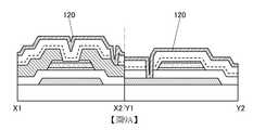
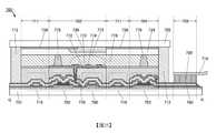
實施方式1在本實施方式中,參照圖1A至圖10B說明本發明的一個實施方式的半導體裝置以及半導體裝置的製造方法。
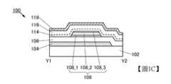
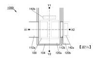
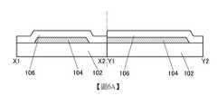
<1-1.半導體裝置的結構例子1>圖1A是作為本發明的一個實施方式的半導體裝置的電晶體100的俯視圖,圖1B相當於沿著圖1A所示的點劃線X1-X2的剖面圖,圖1C相當於沿著圖1A所示的點劃線Y1-Y2的剖面圖。注意,在圖1A中,為了方便起見,省略電晶體100的組件的一部分(被用作閘極絕緣膜的絕緣膜等)而進行圖示。此外,有時將點劃線X1-X2方向稱為通道長度方向,將點劃線Y1-Y2方向稱為通道寬度方向。注意,有時在後面的電晶體的俯視圖中也與圖1A同樣地省略組件的一部分。<1-1. Structure example 1 of semiconductor device>FIG. 1A is a plan view of a
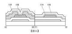
電晶體100包括:基板102上的導電膜104;基板102及導電膜104上的絕緣膜106;絕緣膜106上的氧化物半導體膜108;氧化物半導體膜108上的導電膜112a;以及氧化物半導體膜108上的導電膜112b。此外,在電晶體100上,明確而言,在氧化物半導體膜108、導電膜112a及導電膜112b上形成有絕緣膜114、絕緣膜114上的絕緣膜116以及絕緣膜116上的絕緣膜118。The
另外,電晶體100是所謂通道蝕刻型電晶體。In addition, the
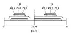
此外,氧化物半導體膜108包括:絕緣膜106上的氧化物半導體膜108_1;氧化物半導體膜108_1上的氧化物半導體膜108_2;以及氧化物半導體膜108_2上的氧化物半導體膜108_3。此外,氧化物半導體膜108_1、氧化物半導體膜108_2及氧化物半導體膜108_3都包含相同的元素。例如,氧化物半導體膜108_1、氧化物半導體膜108_2及氧化物半導體膜108_3較佳為分別獨立地包含In、M(M為Al、Ga、Y或Sn)和Zn。In addition, the
此外,氧化物半導體膜108_1、氧化物半導體膜108_2及氧化物半導體膜108_3較佳為分別獨立地包括In的原子個數比大於M的原子個數比的區域。作為一個例子,較佳為將氧化物半導體膜108_1的In、M及Zn的原子個數比設定為In:M:Zn=4:2:3或其附近。此外,較佳為將氧化物半導體膜108_2的In、M及Zn的原子個數比設定為In:M:Zn=4:2:3或其附近。此外,較佳為將氧化物半導體膜108_3的In、M及Zn的原子個數比設定為In:M:Zn=4:2:3或其附近。在此,“附近”包括:當In為4時,M為1.5以上且2.5以下,並且Zn為2以上且4以下的情況。如此,當氧化物半導體膜108_1、氧化物半導體膜108_2及氧化物半導體膜108_3的組成大致相同時,可以使用相同的濺射靶材,所以可以抑制製造成本。In addition, it is preferable that the oxide semiconductor film 108_1, the oxide semiconductor film 108_2, and the oxide semiconductor film 108_3 independently include regions in which the atomic number ratio of In is greater than the atomic number ratio of M. As an example, it is preferable to set the atomic ratio of In, M, and Zn of the oxide semiconductor film 108_1 to In:M:Zn=4:2:3 or its vicinity. In addition, it is preferable to set the atomic ratio of In, M, and Zn of the oxide semiconductor film 108_2 to In:M:Zn=4:2:3 or its vicinity. In addition, it is preferable to set the atomic ratio of In, M, and Zn of the oxide semiconductor film 108_3 to In:M:Zn=4:2:3 or its vicinity. Here, “nearby” includes: when In is 4, M is 1.5 or more and 2.5 or less, and Zn is 2 or more and 4 or less. In this way, when the oxide semiconductor film 108_1, the oxide semiconductor film 108_2, and the oxide semiconductor film 108_3 have substantially the same composition, the same sputtering target can be used, so the manufacturing cost can be suppressed.
藉由使氧化物半導體膜108_1、氧化物半導體膜108_2及氧化物半導體膜108_3分別獨立地包括其In的原子個數比大於M的原子個數比的區域,可以提高電晶體100的場效移動率。明確而言,電晶體100的場效移動率可以超過10cm2/Vs,較佳的是,電晶體100的場效移動率可以超過30cm2/Vs。By making the oxide semiconductor film 108_1, the oxide semiconductor film 108_2, and the oxide semiconductor film 108_3 each independently include a region where the atomic number ratio of In is greater than the atomic number ratio of M, the field effect movement of the
例如,藉由將上述場效移動率高的電晶體用於生成閘極信號的閘極驅動器,可以提供一種邊框寬度窄(也稱為窄邊框)的顯示裝置。此外,藉由將上述場效移動率高的電晶體用於顯示裝置所包括的供應來自信號線的信號的源極驅動器(尤其是,與源極驅動器所包括的移位暫存器的輸出端子連接的解多工器),可以提供一種與顯示裝置連接的佈線數較少的顯示裝置。For example, by using the above-mentioned transistor with a high field effect rate of movement as a gate driver for generating a gate signal, a display device with a narrow frame width (also called a narrow frame) can be provided. In addition, by using the above-mentioned transistor with high field-effect mobility for the source driver included in the display device that supplies the signal from the signal line (especially, with the output terminal of the shift register included in the source driver) Connected demultiplexer) can provide a display device with a small number of wires connected to the display device.
另一方面,即使氧化物半導體膜108_1、氧化物半導體膜108_2及氧化物半導體膜108_3分別獨立地包括In的原子個數比大於M的原子個數比的區域,在氧化物半導體膜108_1、氧化物半導體膜108_2及氧化物半導體膜108_3的結晶性都高的情況下,場效移動率有時下降。On the other hand, even if the oxide semiconductor film 108_1, the oxide semiconductor film 108_2, and the oxide semiconductor film 108_3 each independently include a region where the atomic number ratio of In is greater than the atomic number ratio of M, the oxide semiconductor film 108_1 is oxidized When the crystallinity of the material semiconductor film 108_2 and the oxide semiconductor film 108_3 are both high, the field effect mobility may decrease.
但是,在本發明的一個實施方式的半導體裝置中,氧化物半導體膜108_2包括其結晶性比氧化物半導體膜108_1和氧化物半導體膜108_3中的一者或兩者低的區域。此外,氧化物半導體膜108的結晶性例如可以藉由X射線繞射(XRD:X-Ray Diffraction)或穿透式電子顯微鏡(TEM:Transmission Electron Microscope)進行分析。However, in the semiconductor device of one embodiment of the present invention, the oxide semiconductor film 108_2 includes a region whose crystallinity is lower than one or both of the oxide semiconductor film 108_1 and the oxide semiconductor film 108_3. In addition, the crystallinity of the
在氧化物半導體膜108_2包括結晶性低的區域的情況下,發揮如下優異的效果。When the oxide semiconductor film 108_2 includes a region with low crystallinity, the following excellent effects are exhibited.
首先,對在氧化物半導體膜108中可能形成的氧空位進行說明。First, the oxygen vacancies that may be formed in the
另外,形成在氧化物半導體膜108中的氧空位對電晶體特性造成影響而引起問題。例如,當在氧化物半導體膜108中形成有氧空位時,該氧空位與氫鍵合,而成為載子供應源。當在氧化物半導體膜108中產生載子供應源時,具有氧化物半導體膜108的電晶體100的電特性發生變動,典型為臨界電壓的漂移。因此,在氧化物半導體膜108中,氧空位越少越好。In addition, the oxygen vacancies formed in the
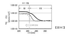
於是,在本發明的一個實施方式中,位於氧化物半導體膜108附近的絕緣膜,明確而言,形成在氧化物半導體膜108上方的絕緣膜114、116包含過量氧。藉由使氧或過量氧從絕緣膜114、116移動到氧化物半導體膜108,能夠減少氧化物半導體膜中的氧空位。Therefore, in one embodiment of the present invention, the insulating film located near the
在此,參照圖10A和圖10B對擴散到氧化物半導體膜108中的氧或過量氧的路徑進行說明。圖10A和圖10B是表示擴散到氧化物半導體膜108中的氧或過量氧的擴散路徑的示意圖,圖10A是通道長度方向上的示意圖,圖10B是通道寬度方向上的示意圖。Here, the path of oxygen or excess oxygen diffused into the
絕緣膜114、116所包含的氧或過量氧從上方,亦即經過氧化物半導體膜108_3而擴散到氧化物半導體膜108_2和氧化物半導體膜108_1中(圖10A和圖10B所示的Route 1)。Oxygen or excess oxygen contained in the insulating
或者,絕緣膜114、116所包含的氧或過量氧從氧化物半導體膜108_1、氧化物半導體膜108_2及氧化物半導體膜108_3的每個側面擴散到氧化物半導體膜108中(圖10B所示的Route 2)。Alternatively, oxygen or excess oxygen contained in the insulating
例如,在圖10A和圖10B所示的Route 1中,在氧化物半導體膜108_3的結晶性高時,有時妨礙氧或過量氧的擴散。另一方面,在圖10B所示的Route 2中,可以將氧或過量氧從氧化物半導體膜108_1、氧化物半導體膜108_2及氧化物半導體膜108_3的每個側面擴散到氧化物半導體膜108_1、氧化物半導體膜108_2及氧化物半導體膜108_3中。For example, in
此外,在圖10B所示的Route 2中,包括氧化物半導體膜108_2的結晶性比氧化物半導體膜108_1及氧化物半導體膜108_3的結晶性低的區域,所以該區域成為過量氧的擴散路徑,可以將過量氧擴散到其結晶性比氧化物半導體膜108_2高的氧化物半導體膜108_1及氧化物半導體膜108_3中。因此,在氧化物半導體膜108_2的厚度比氧化物半導體膜108_1及氧化物半導體膜108_3大時,氧的擴散路徑變大,所以是較佳的。此外,雖然圖10A和圖10B未圖示,但是在絕緣膜106包含氧或過量氧的情況下,氧或過量氧有可能從絕緣膜106還擴散到氧化物半導體膜108中。In addition, in
如此,在本發明的一個實施方式的半導體裝置中,採用結晶結構不同的氧化物半導體膜的疊層結構,將結晶性低的區域用作過量氧的擴散路徑,由此可以提供一種可靠性高的半導體裝置。In this way, in the semiconductor device of one embodiment of the present invention, a stacked structure of oxide semiconductor films with different crystal structures is adopted, and regions with low crystallinity are used as diffusion paths for excess oxygen, thereby providing a highly reliable Of semiconductor devices.
此外,在只使用結晶性低的氧化物半導體膜構成氧化物半導體膜108的情況下,雜質(例如,氫或水分等)附著於或者混入到背後通道一側,亦即相當於氧化物半導體膜108_3的區域中,有時導致可靠性的下降。In addition, when only an oxide semiconductor film with low crystallinity is used to form the
混入到氧化物半導體膜108中的氫或水分等雜質影響到電晶體特性,所以成為問題。因此,在氧化物半導體膜108中,氫或水分等雜質越少越佳。Impurities such as hydrogen and moisture mixed into the
於是,在本發明的一個實施方式中,藉由提高氧化物半導體膜的下層及上層的氧化物半導體膜的結晶性,可以抑制可能混入到氧化物半導體膜108中的雜質。尤其是,藉由提高氧化物半導體膜108_3的結晶性,可以抑制對導電膜112a、112b進行加工時的損傷。當對導電膜112a、112b進行加工時,氧化物半導體膜108的表面,亦即氧化物半導體膜108_3的表面暴露於蝕刻劑或蝕刻氣體。但是,因為氧化物半導體膜108_3包括結晶性高的區域,所以被用作蝕刻停止層。Therefore, in one embodiment of the present invention, by increasing the crystallinity of the lower and upper oxide semiconductor films of the oxide semiconductor film, impurities that may be mixed into the
藉由作為氧化物半導體膜108使用雜質濃度低且缺陷態密度低的氧化物半導體膜,可以製造具有優良的電特性的電晶體,所以是較佳的。這裡,將雜質濃度低且缺陷態密度低(氧空位少)的狀態稱為“高純度本質”或“實質上高純度本質”。因為高純度本質或實質上高純度本質的氧化物半導體膜的載子發生源較少,所以可以降低載子密度。因此,在該氧化物半導體膜中形成有通道區域的電晶體很少具有負臨界電壓的電特性(也稱為常開啟特性)。因為高純度本質或實質上高純度本質的氧化物半導體膜具有較低的缺陷態密度,所以有可能具有較低的陷阱態密度。高純度本質或實質上高純度本質的氧化物半導體膜的關態電流顯著小,即便是通道寬度W為1×106µm、通道長度L為10µm的元件,當源極電極與汲極電極間的電壓(汲極電壓)在1V至10V的範圍時,關態電流也可以為半導體參數分析儀的測量極限以下,亦即1×10-13A以下。By using an oxide semiconductor film with a low impurity concentration and a low defect state density as the
此外,在氧化物半導體膜108_2具有其結晶性比氧化物半導體膜108_1及氧化物半導體膜108_3低的區域時,載子密度有時得到提高。In addition, when the oxide semiconductor film 108_2 has a region whose crystallinity is lower than that of the oxide semiconductor film 108_1 and the oxide semiconductor film 108_3, the carrier density may be increased.
此外,當氧化物半導體膜108_2的載子密度較高時,費米能階有時相對地高於氧化物半導體膜108_2的導帶。由此,氧化物半導體膜108_2的導帶底變低,氧化物半導體膜108_2的導帶底與可能形成在閘極絕緣膜(在此,絕緣膜106)中的陷阱能階的能量差有時變大。當該能量差變大時,在閘極絕緣膜中被俘獲的電荷變少,有時可以減少電晶體的臨界電壓變動。此外,當氧化物半導體膜108_2的載子密度得到提高時,可以提高氧化物半導體膜108的場效移動率。In addition, when the carrier density of the oxide semiconductor film 108_2 is high, the Fermi level is sometimes relatively higher than the conduction band of the oxide semiconductor film 108_2. As a result, the conduction band bottom of the oxide semiconductor film 108_2 becomes lower, and the energy difference between the conduction band bottom of the oxide semiconductor film 108_2 and the trap level that may be formed in the gate insulating film (here, the insulating film 106) is sometimes Get bigger. When the energy difference becomes large, the charge trapped in the gate insulating film decreases, and the threshold voltage variation of the transistor can be reduced in some cases. In addition, when the carrier density of the oxide semiconductor film 108_2 is increased, the field effect mobility of the
此外,氧化物半導體膜108_2較佳為複合氧化物半導體,包括:具有InaMbZncOd(M表示Al、Ga、Y或Sn,a、b、c及d表示任意數)的第一區域;以及具有InxZnyOz(x、y及z表示任意數)的第二區域。關於該複合氧化物半導體膜,將在實施方式2中進行詳細說明。In addition, the oxide semiconductor film 108_2 is preferably a composite oxide semiconductor, and includes: a second layer having Ina Mb Znc Od (M represents Al, Ga, Y, or Sn, a, b, c, and d represent arbitrary numbers) A region; and a second region with Inx Zny Oz (x, y, and z represent arbitrary numbers). This composite oxide semiconductor film will be described in detail in
另外,在圖1A至圖1C所示的電晶體100中,絕緣膜106具有電晶體100的閘極絕緣膜的功能,絕緣膜114、116、118具有電晶體100的保護絕緣膜的功能。此外,在電晶體100中,導電膜104具有閘極電極的功能,導電膜112a具有源極電極的功能,導電膜112b具有汲極電極的功能。注意,在本說明書等中,有時將絕緣膜106稱為第一絕緣膜,將絕緣膜114、116稱為第二絕緣膜,將絕緣膜118稱為第三絕緣膜。In addition, in the
<1-2.半導體裝置的組件>以下,對本實施方式的半導體裝置所包括的組件進行詳細的說明。<1-2. Components of semiconductor device>Hereinafter, the components included in the semiconductor device of this embodiment will be described in detail.
[基板]雖然對基板102的材料等沒有特別的限制,但是至少需要能夠承受後續的加熱處理的耐熱性。例如,作為基板102,可以使用玻璃基板、陶瓷基板、石英基板、藍寶石基板等。另外,還可以使用以矽或碳化矽為材料的單晶半導體基板或多晶半導體基板、以矽鍺等為材料的化合物半導體基板、SOI(Silicon On Insulator:絕緣層上覆矽)基板等,並且也可以將設置有半導體元件的上述基板用作基板102。當作為基板102使用玻璃基板時,藉由使用第六代(1500mm×1850mm)、第七代(1870mm×2200mm)、第八代(2200mm×2400mm)、第九代(2400mm×2800mm)、第十代(2950mm×3400mm)等的大面積基板,可以製造大型顯示裝置。[Substrate]Although there are no particular restrictions on the material and the like of the
作為基板102,也可以使用撓性基板,並且在撓性基板上直接形成電晶體100。或者,也可以在基板102與電晶體100之間設置剝離層。剝離層可以在如下情況下使用,亦即在剝離層上製造半導體裝置的一部分或全部,然後將其從基板102分離並轉置到其他基板上的情況。此時,也可以將電晶體100轉置到耐熱性低的基板或撓性基板上。As the
[導電膜]被用作閘極電極的導電膜104、被用作源極電極的導電膜112a及被用作汲極電極的導電膜112b可以使用選自鉻(Cr)、銅(Cu)、鋁(Al)、金(Au)、銀(Ag)、鋅(Zn)、鉬(Mo)、鉭(Ta)、鈦(Ti)、鎢(W)、錳(Mn)、鎳(Ni)、鐵(Fe)、鈷(Co)中的金屬元素、以上述金屬元素為成分的合金或者組合上述金屬元素的合金等形成。[Conductive Film]The
另外,作為導電膜104、112a、112b,也可以使用包含銦和錫的氧化物(In-Sn氧化物)、包含銦和鎢的氧化物(In-W氧化物)、包含銦、鎢及鋅的氧化物(In-W-Zn氧化物)、包含銦和鈦的氧化物(In-Ti氧化物)、包含銦、鈦及錫的氧化物(In-Ti-Sn氧化物)、包含銦和鋅的氧化物(In-Zn氧化物)、包含銦、錫及矽的氧化物(In-Sn-Si氧化物)、包含銦、鎵及鋅的氧化物(In-Ga-Zn氧化物)等氧化物導電體或氧化物半導體。In addition, as the
在此,說明氧化物導電體。在本說明書等中,也可以將氧化物導電體稱為OC(Oxide Conductor)。例如,在氧化物半導體中形成氧空位,對該氧空位添加氫而在導帶附近形成施體能階。其結果,氧化物半導體的導電性增高,而成為導電體。可以將成為導電體的氧化物半導體稱為氧化物導電體。一般而言,由於氧化物半導體的能隙大,因此對可見光具有透光性。另一方面,氧化物導電體是在導帶附近具有施體能階的氧化物半導體。因此,在氧化物導電體中,起因於施體能階的吸收的影響小,而對可見光具有與氧化物半導體大致相同的透光性。Here, the oxide conductor will be described. In this specification and the like, the oxide conductor may also be referred to as OC (Oxide Conductor). For example, an oxygen vacancy is formed in an oxide semiconductor, and hydrogen is added to the oxygen vacancy to form a donor level near the conduction band. As a result, the conductivity of the oxide semiconductor increases and becomes a conductor. An oxide semiconductor that becomes a conductor can be referred to as an oxide conductor. Generally speaking, since oxide semiconductors have a large energy gap, they are transparent to visible light. On the other hand, the oxide conductor is an oxide semiconductor having a donor energy level near the conduction band. Therefore, in the oxide conductor, the influence caused by the absorption of the donor energy level is small, and the visible light has substantially the same light transmittance as that of an oxide semiconductor.
另外,作為導電膜104、112a、112b,也可以應用Cu-X合金膜(X為Mn、Ni、Cr、Fe、Co、Mo、Ta或Ti)。藉由使用Cu-X合金膜,可以以濕蝕刻製程進行加工,從而可以抑制製造成本。In addition, as the
此外,導電膜112a、112b尤其較佳為包含上述金屬元素中的銅、鈦、鎢、鉭和鉬中的一個或多個。尤其是,作為導電膜112a、112b,較佳為使用氮化鉭膜。該氮化鉭膜具有導電性且具有對銅或氫的高阻擋性。此外,因為從氮化鉭膜本身釋放的氫少,所以可以作為與氧化物半導體膜108接觸的導電膜或氧化物半導體膜108的附近的導電膜最適合地使用氮化鉭膜。此外,當作為導電膜112a、112b使用銅膜時,可以降低導電膜112a、112b的電阻,所以是較佳的。In addition, it is particularly preferable that the
可以藉由無電鍍法形成導電膜112a、112b。作為藉由該無電鍍法可形成的材料,例如可以使用選自Cu、Ni、Al、Au、Sn、Co、Ag和Pd中的一個或多個。尤其是,由於在使用Cu或Ag時,可以降低導電膜的電阻,所以是較佳的。The
[被用作閘極絕緣膜的絕緣膜]作為被用作電晶體100的閘極絕緣膜的絕緣膜106,可以藉由電漿增強化學氣相沉積(PECVD:Plasma Enhanced Chemical Vapor Deposition)法、濺射法等形成包括氧化矽膜、氧氮化矽膜、氮氧化矽膜、氮化矽膜、氧化鋁膜、氧化鉿膜、氧化釔膜、氧化鋯膜、氧化鎵膜、氧化鉭膜、氧化鎂膜、氧化鑭膜、氧化鈰膜和氧化釹膜中的一種以上的絕緣層。注意,絕緣膜106也可以具有兩層以上的疊層結構。[Insulating film used as gate insulating film]As the insulating
此外,較佳的是,與被用作電晶體100的通道區域的氧化物半導體膜108接觸的絕緣膜106為氧化物絕緣膜,更佳的是,該氧化物絕緣膜具有氧含量超過化學計量組成的區域(過量氧區域)。換言之,絕緣膜106能夠釋放氧。為了在絕緣膜106中形成過量氧區域,例如可以採用如下方法:在氧氛圍下形成絕緣膜106;或者在氧氛圍下對成膜之後的絕緣膜106進行加熱處理。In addition, it is preferable that the insulating
此外,當絕緣膜106使用氧化鉿時發揮如下效果。氧化鉿的相對介電常數比氧化矽或氧氮化矽高。因此,藉由使用氧化鉿,與使用氧化矽的情況相比,可以使絕緣膜106的厚度變大,由此,可以減少穿隧電流引起的洩漏電流。亦即,可以實現關態電流小的電晶體。再者,與具有非晶結構的氧化鉿相比,具有結晶結構的氧化鉿具有高相對介電常數。因此,為了形成關態電流小的電晶體,較佳為使用具有結晶結構的氧化鉿。作為結晶結構的例子,可以舉出單斜晶系或立方晶系等。注意,本發明的一個實施方式不侷限於此。In addition, when hafnium oxide is used for the insulating
注意,在本實施方式中,作為絕緣膜106形成氮化矽膜和氧化矽膜的疊層膜。與氧化矽膜相比,氮化矽膜的相對介電常數較高且為了得到與氧化矽膜相等的靜電容量所需要的厚度較大,因此,藉由使電晶體100的閘極絕緣膜包括氮化矽膜,可以增加絕緣膜的厚度。因此,可以藉由抑制電晶體100的絕緣耐壓的下降並提高絕緣耐壓來抑制電晶體100的靜電破壞。Note that in this embodiment mode, a laminated film of a silicon nitride film and a silicon oxide film is formed as the insulating
[氧化物半導體膜]作為氧化物半導體膜108可以使用上述材料。[Oxide Semiconductor Film]As the
當氧化物半導體膜108為In-M-Zn氧化物時,用來形成In-M-Zn氧化物的濺射靶材的金屬元素的原子個數比較佳為滿足In>M。作為這種濺射靶材的金屬元素的原子個數比,可以舉出In:M:Zn=2:1:3、In:M:Zn=3:1:2、In:M:Zn=4:2:4.1、In:M:Zn=5:1:6、In:M:Zn=5:1:8、In:M:Zn=6:1:6、In:M:Zn=5:2:5等。When the
另外,當氧化物半導體膜108為In-M-Zn氧化物時,作為濺射靶材較佳為使用包含多晶的In-M-Zn氧化物的靶材。藉由使用包含多晶的In-M-Zn氧化物的靶材,容易形成具有結晶性的氧化物半導體膜108。注意,所形成的氧化物半導體膜108的原子個數比分別包含上述濺射靶材中的金屬元素的原子個數比的±40%的範圍內。例如,在被用於氧化物半導體膜108的濺射靶材的組成為In:Ga:Zn=4:2:4.1[原子個數比]時,所形成的氧化物半導體膜108的組成有時為In:Ga:Zn=4:2:3[原子個數比]附近。In addition, when the
氧化物半導體膜108的能隙為2eV以上,較佳為2.5eV以上。如此,藉由使用能隙較寬的氧化物半導體,可以降低電晶體100的關態電流。The energy gap of the
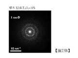
氧化物半導體膜108較佳為具有非單晶結構。非單晶結構例如包括下述CAAC-OS(C Axis Aligned Crystalline Oxide Semiconductor:c軸配向結晶氧化物半導體)、多晶結構、微晶結構或非晶結構。在非單晶結構中,非晶結構的缺陷態密度最高,而CAAC-OS的缺陷態密度最低。The
[被用作保護絕緣膜的絕緣膜 1]絕緣膜114、116被用作電晶體100的保護絕緣膜。另外,絕緣膜114、116具有對氧化物半導體膜108供應氧的功能。亦即,絕緣膜114、116包含氧。另外,絕緣膜114是能夠使氧透過的絕緣膜。注意,絕緣膜114還被用作在後面形成絕緣膜116時緩解對氧化物半導體膜108造成的損傷的膜。[Insulation film used as a protective insulating film 1]The insulating
作為絕緣膜114,可以使用厚度為5nm以上且150nm以下,較佳為5nm以上且50nm以下的氧化矽膜、氧氮化矽膜等。As the insulating
此外,較佳為使絕緣膜114中的缺陷量較少,典型的是,藉由電子自旋共振(ESR:Electron Spin Resonance)測得的起因於矽懸空鍵且在g=2.001處出現的信號的自旋密度較佳為3×10¹⁷spins/cm3以下。這是因為,若絕緣膜114的缺陷密度高,氧則與該缺陷鍵合,而使絕緣膜114中的氧的透過性減少的緣故。In addition, it is preferable to make the amount of defects in the insulating
在絕緣膜114中,有時從外部進入絕緣膜114的氧不是全部移動到絕緣膜114的外部,而是其一部分殘留在絕緣膜114內部。另外,有時在氧從外部進入絕緣膜114的同時,絕緣膜114所含有的氧移動到絕緣膜114的外部,由此在絕緣膜114中發生氧的移動。在形成能夠使氧透過的氧化物絕緣膜作為絕緣膜114時,可以使從設置在絕緣膜114上的絕緣膜116脫離的氧經過絕緣膜114而移動到氧化物半導體膜108中。In the insulating
此外,絕緣膜114可以使用起因於氮氧化物的態密度低的氧化物絕緣膜形成。注意,該起因於氮氧化物的態密度有時會形成在氧化物半導體膜的價帶頂的能量(EV_OS)與氧化物半導體膜的導帶底的能量(EC_OS)之間。作為上述氧化物絕緣膜,可以使用氮氧化物的釋放量少的氧氮化矽膜或氮氧化物的釋放量少的氧氮化鋁膜等。In addition, the insulating
此外,在熱脫附譜分析法(TDS:Thermal Desorption Spectroscopy)中,氮氧化物的釋放量少的氧氮化矽膜是氨釋放量比氮氧化物的釋放量多的膜,典型的是氨的釋放量為1×1018cm-3以上且5×1019cm-3以下。注意,該氨釋放量是在進行膜表面溫度為50℃以上且650℃以下,較佳為50℃以上且550℃以下的加熱處理時的釋放量。In addition, in the thermal desorption spectroscopy (TDS: Thermal Desorption Spectroscopy), the silicon oxynitride membrane with a small amount of nitrogen oxide release is a membrane that releases more ammonia than nitrogen oxides, and is typically ammonia The release amount of 1×1018 cm-3 or more and 5×1019 cm-3 or less. Note that the ammonia released amount is the released amount when the film surface temperature is 50° C. or higher and 650° C. or lower, preferably 50° C. or higher and 550° C. or lower.
氮氧化物(NOx,x大於0且為2以下,較佳為1以上且2以下),典型的是NO2或NO在絕緣膜114等中形成能階。該能階位於氧化物半導體膜108的能隙中。由此,當氮氧化物擴散到絕緣膜114與氧化物半導體膜108的介面時,有時該能階在絕緣膜114一側俘獲電子。其結果,被俘獲的電子留在絕緣膜114與氧化物半導體膜108的介面附近,由此使電晶體的臨界電壓向正方向漂移。Nitrogen oxides (NOx , x is greater than 0 and 2 or less, preferably 1 or more and 2 or less), typically NO2 or NO forms an energy level in the insulating
另外,當進行加熱處理時,氮氧化物與氨及氧起反應。當進行加熱處理時,絕緣膜114所包含的氮氧化物與絕緣膜116所包含的氨起反應,由此絕緣膜114所包含的氮氧化物減少。因此,在絕緣膜114與氧化物半導體膜108的介面不容易俘獲電子。In addition, when heat treatment is performed, nitrogen oxides react with ammonia and oxygen. When the heat treatment is performed, the nitrogen oxide contained in the insulating
藉由作為絕緣膜114使用上述氧化物絕緣膜,可以降低電晶體的臨界電壓的漂移,從而可以降低電晶體的電特性變動。By using the above-mentioned oxide insulating film as the insulating
藉由電晶體的製程中的加熱處理,典型的是300℃以上且低於350℃的加熱處理,在利用100K以下的ESR對絕緣膜114進行測量而得到的ESR譜中,觀察到g值為2.037以上且2.039以下的第一信號、g值為2.001以上且2.003以下的第二信號以及g值為1.964以上且1.966以下的第三信號。在X帶的ESR測量中,第一信號與第二信號之間的分割寬度(split width)及第二信號與第三信號之間的分割寬度為5mT左右。另外,g值為2.037以上且2.039以下的第一信號、g值為2.001以上且2.003以下的第二信號以及g值為1.964以上且1.966以下的第三信號的自旋密度的總和低於1×10¹⁸spins/cm3,典型為1×1017spins/cm3以上且低於1×1018spins/cm3。By the heat treatment in the manufacturing process of the transistor, typically a heat treatment above 300°C and lower than 350°C, in the ESR spectrum obtained by measuring the insulating
在100K以下的ESR譜中,g值為2.037以上且2.039以下的第一信號、g值為2.001以上且2.003以下的第二信號以及g值為1.964以上且1.966以下的第三信號的自旋密度的總數相當於起因於氮氧化物(NOx,x大於0且為2以下,較佳為1以上且2以下)的信號的自旋密度的總數。作為氮氧化物的典型例子,有一氧化氮、二氧化氮等。亦即,g值為2.037以上且2.039以下的第一信號、g值為2.001以上且2.003以下的第二信號以及g值為1.964以上且1.966以下的第三信號的自旋密度的總數越少,氧化物絕緣膜中的氮氧化物含量越少。In the ESR spectrum below 100K, the spin density of the first signal with a g value of 2.037 or more and 2.039 or less, the second signal with a g value of 2.001 or more and 2.003 or less, and the third signal with a g value of 1.964 or more and 1.966 or less corresponds to the total number of the total number of nitrogen oxides due to the spin density signal (NOx, x is greater than 0 and 2 or less, preferably 1 or more and 2 or less). As typical examples of nitrogen oxides, nitrogen monoxide, nitrogen dioxide, and the like. That is, the total number of spin densities of the first signal having a g value of 2.037 or more and 2.039 or less, the second signal having a g value of 2.001 or more and 2.003 or less, and the third signal having a g value of 1.964 or more and 1.966 or less, the smaller the total number of spin densities, The lower the content of oxynitride in the oxide insulating film.
另外,上述氧化物絕緣膜的利用SIMS測得的氮濃度為6×10²⁰atoms/cm3以下。In addition, the oxide insulating film has a nitrogen concentration measured by SIMS of 6×10²⁰ atoms/cm3 or less.
藉由在基板溫度為220℃以上且350℃以下的情況下利用使用矽烷及一氧化二氮的PECVD法形成上述氧化物絕緣膜,可以形成緻密且硬度高的膜。By forming the above-mentioned oxide insulating film by a PECVD method using silane and nitrous oxide when the substrate temperature is 220° C. or higher and 350° C. or lower, a dense and high-hardness film can be formed.
絕緣膜116為氧含量超過化學計量組成的氧化物絕緣膜。上述氧化物絕緣膜由於被加熱而其一部分的氧脫離。另外,在TDS中,上述氧化物絕緣膜包括氧釋放量為1.0×10¹⁹atoms/cm3以上,較佳為3.0×1020atoms/cm3以上的區域。注意,上述氧釋放量是在TDS中的加熱處理的溫度為50℃以上且650℃以下或者50℃以上且550℃以下的範圍內被釋放的氧的總量。此外,上述氧釋放量為在TDS中換算為氧原子的總量。The insulating
作為絕緣膜116可以使用厚度為30nm以上且500nm以下,較佳為50nm以上且400nm以下的氧化矽膜、氧氮化矽膜等。As the insulating
此外,較佳為使絕緣膜116中的缺陷量較少,典型的是,藉由ESR測得的起因於矽懸空鍵且在g=2.001處出現的信號的自旋密度低於1.5×10¹⁸spins/cm3,更佳為1×1018spins/cm3以下。由於絕緣膜116與絕緣膜114相比離氧化物半導體膜108更遠,所以絕緣膜116的缺陷密度也可以高於絕緣膜114。In addition, it is preferable to make the amount of defects in the insulating
另外,因為絕緣膜114、116可以使用相同種類材料形成,所以有時無法明確地確認到絕緣膜114與絕緣膜116的介面。因此,在本實施方式中,以虛線圖示出絕緣膜114與絕緣膜116的介面。注意,在本實施方式中,雖然說明絕緣膜114與絕緣膜116的兩層結構,但是不侷限於此,例如,也可以採用絕緣膜114的單層結構或三層以上的疊層結構。In addition, since the insulating
[被用作保護絕緣膜的絕緣膜 2]絕緣膜118被用作電晶體100的保護絕緣膜。[Insulating film used as a protective insulating film 2]The insulating
絕緣膜118包含氫和氮中的一者或兩者。或者,絕緣膜118包含氮及矽。絕緣膜118具有阻擋氧、氫、水、鹼金屬、鹼土金屬等的功能。藉由設置絕緣膜118,能夠防止氧從氧化物半導體膜108擴散到外部並能夠防止絕緣膜114、116所包含的氧擴散到外部,還能夠抑制氫、水等從外部侵入氧化物半導體膜108中。The insulating
作為絕緣膜118,例如可以使用氮化物絕緣膜。作為該氮化物絕緣膜,有氮化矽、氮氧化矽、氮化鋁、氮氧化鋁等。As the insulating
雖然上述所記載的導電膜、絕緣膜及氧化物半導體膜等各種膜可以利用濺射法或PECVD法形成,但是例如也可以利用其它方法,例如熱CVD(Chemical Vapor Deposition:化學氣相沉積)法形成。作為熱CVD法的例子,可以舉出MOCVD(Metal Organic Chemical Vapor Deposition:有機金屬化學氣相沉積)法或ALD(Atomic Layer Deposition:原子層沉積)法等。Although the conductive films, insulating films, and oxide semiconductor films described above can be formed by sputtering or PECVD, other methods such as thermal CVD (Chemical Vapor Deposition) can also be used. form. As an example of the thermal CVD method, a MOCVD (Metal Organic Chemical Vapor Deposition) method, an ALD (Atomic Layer Deposition) method, or the like can be cited.
由於熱CVD法是不使用電漿的成膜方法,因此具有不產生因電漿損傷引起的缺陷的優點。此外,可以以如下方法進行熱CVD法:將源氣體供應到處理室內,將處理室內的壓力設定為大氣壓或減壓而在基板上沉積膜。Since the thermal CVD method is a film formation method that does not use plasma, it has the advantage of not generating defects due to plasma damage. In addition, the thermal CVD method may be performed in a method in which a source gas is supplied into the processing chamber, and the pressure in the processing chamber is set to atmospheric pressure or reduced pressure to deposit a film on the substrate.
此外,可以以如下方法進行ALD法:將源氣體供應到處理室內,將處理室內的壓力設定為大氣壓或減壓而在基板上沉積膜。In addition, the ALD method may be performed in a method in which a source gas is supplied into the processing chamber, and the pressure in the processing chamber is set to atmospheric pressure or reduced pressure to deposit a film on the substrate.
藉由MOCVD法或ALD法等熱CVD法可以形成上述實施方式所述的導電膜、絕緣膜、氧化物半導體膜等各種膜,例如,當形成In-Ga-Zn-O膜時,使用三甲基銦、三甲基鎵及二甲基鋅。三甲基銦的化學式為In(CH3)3。三甲基鎵的化學式為Ga(CH3)3。另外,二甲基鋅的化學式為Zn(CH3)2。另外,不侷限於上述組合,也可以使用三乙基鎵(化學式為Ga(C2H5)3)代替三甲基鎵,並使用二乙基鋅(化學式為Zn(C2H5)2)代替二甲基鋅。Various films such as conductive films, insulating films, and oxide semiconductor films described in the above embodiments can be formed by thermal CVD methods such as the MOCVD method or the ALD method. For example, when forming an In-Ga-Zn-O film, use three Base indium, trimethylgallium and dimethylzinc. The chemical formula of trimethylindium is In(CH3 )3 . The chemical formula of trimethylgallium is Ga(CH3 )3 . In addition, the chemical formula of dimethyl zinc is Zn(CH3 )2 . In addition, it is not limited to the above combination. Triethylgallium (chemical formula is Ga(C2 H5 )3 ) can also be used instead of trimethylgallium, and diethyl zinc (chemical formula is Zn(C2 H5 )2) ) Instead of dimethyl zinc.
例如,在使用利用ALD法的成膜裝置形成氧化鉿膜時,使用如下兩種氣體:藉由使包含溶劑和鉿前體化合物的液體(鉿醇鹽、四二甲基醯胺鉿(TDMAH)等鉿醯胺)氣化而得到的源氣體;以及用作氧化劑的臭氧(O3)。此外,四二甲基醯胺鉿的化學式為Hf[N(CH3)2]4。另外,作為其他材料液有四(乙基甲基醯胺)鉿等。For example, when a hafnium oxide film is formed using a film forming apparatus using the ALD method, the following two gases are used: by making a liquid containing a solvent and a hafnium precursor compound (hafnium alkoxide, tetradimethyl amide hafnium (TDMAH) The source gas obtained by the gasification of hafnium amine); and ozone (O3 ) used as an oxidant. In addition, the chemical formula of Hafnium Tetradimethylamide is Hf[N(CH3 )2 ]4 . In addition, as other material liquids, there are tetrakis (ethyl methyl amide) hafnium and the like.
例如,在使用利用ALD法的成膜裝置形成氧化鋁膜時,使用如下兩種氣體:藉由使包含溶劑和鋁前體化合物的液體(三甲基鋁(TMA)等)氣化而得到的源氣體;以及用作氧化劑的H2O。此外,三甲基鋁的化學式為Al(CH3)3。另外,作為其他材料液有三(二甲基醯胺)鋁、三異丁基鋁、鋁三(2,2,6,6-四甲基-3,5-庚二酮)等。For example, when forming an aluminum oxide film using a film forming apparatus using the ALD method, the following two gases are used: those obtained by vaporizing a liquid (trimethylaluminum (TMA), etc.) containing a solvent and an aluminum precursor compound Source gas; and H2 O used as an oxidant. In addition, the chemical formula of trimethylaluminum is Al(CH3 )3 . In addition, as other material liquids, there are tris(dimethylamide) aluminum, triisobutyl aluminum, aluminum tris(2,2,6,6-tetramethyl-3,5-heptanedione), and the like.
例如,在使用利用ALD法的成膜裝置形成氧化矽膜時,使六氯乙矽烷附著在被成膜面上,去除附著物所包含的氯,供應氧化性氣體(O2、一氧化二氮)的自由基使其與附著物起反應。For example, when a silicon oxide film is formed using a film-forming device using the ALD method, hexachloroethane is attached to the film-forming surface to remove the chlorine contained in the attached matter and supply oxidizing gas (O2 , nitrous oxide) ) Free radicals make it react with attachments.
例如,在使用利用ALD法的成膜裝置形成鎢膜時,使用WF6氣體和B2H6氣體形成第一鎢膜,然後使用WF6氣體和H2氣體形成第二鎢膜。注意,也可以使用SiH4氣體代替B2H6氣體。For example, when a tungsten film is formed using a film forming apparatus using the ALD method, a first tungsten film is formedusing WF 6 gas and B2 H6 gas, and then a second tungsten film is formedusing WF 6 gas and H2 gas.Note that SiH 4 gas can also be used instead of B2 H6 gas.
例如,在使用利用ALD法的成膜裝置形成氧化物半導體膜如In-Ga-Zn-O膜時,使用In(CH3)3氣體和O3氣體形成In-O層,然後使用Ga(CH3)3氣體和O3氣體形成GaO層,之後使用Zn(CH3)2氣體和O3氣體形成ZnO層。注意,這些層的順序不侷限於上述例子。此外,也可以混合這些氣體來形成混合化合物層如In-Ga-O層、In-Zn-O層、Ga-Zn-O層等。注意,雖然也可以使用利用Ar等惰性氣體對水進行起泡而得到的H2O氣體代替O3氣體,但是較佳為使用不包含H的O3氣體。另外,也可以使用In(C2H5)3氣體代替In(CH3)3氣體。此外,也可以使用Ga(C2H5)3氣體代替Ga(CH3)3氣體。另外,也可以使用Zn(CH3)2氣體。For example, when an oxide semiconductor film such as an In-Ga-Zn-O film is formed using a film forming apparatus using the ALD method, In(CH3 )3 gas and O3 gas are used to form the In-O layer, and then Ga(CH3 )3 gas and O3 gas are used to form a GaO layer, and then Zn(CH3 )2 gas and O3 gas are used to form a ZnO layer. Note that the order of these layers is not limited to the above example. In addition, these gases can also be mixed to form a mixed compound layer such as an In-Ga-O layer, an In-Zn-O layer, a Ga-Zn-O layer, and the like. Note that, although it may be used for H2 O gas bubbling water using an inert gas such as Ar obtained instead of the O3 gas, but preferably does not contain H O3 gas. In addition, In(C2 H5 )3 gas may be used instead of In(CH3 )3 gas. In addition, Ga(C2 H5 )3 gas may be used instead of Ga(CH3 )3 gas. In addition, Zn(CH3 )2 gas can also be used.
<1-3.半導體裝置的結構例子2>接著,使用圖2A至圖5C說明與圖1A至圖1C所示的電晶體100的變形例子。<1-3. Structure example 2 of semiconductor device>Next, a modification example of the
圖2A是作為本發明的一個實施方式的半導體裝置的電晶體100A的俯視圖,圖2B相當於沿著圖2A所示的點劃線X1-X2的剖面圖,圖2C相當於沿著圖2A所示的點劃線Y1-Y2的剖面圖。2A is a plan view of a
圖2A至圖2C所示的電晶體100A具有所謂通道保護型電晶體結構。如此,本發明的一個實施方式的半導體裝置可以具有通道蝕刻型電晶體結構或通道保護型電晶體結構。The
此外,在電晶體100A中,絕緣膜114、116包括開口部141a、141b。此外,氧化物半導體膜108藉由開口部141a、141b與導電膜112a、112b連接。此外,在導電膜112a、112b上形成有絕緣膜118。此外,絕緣膜114、116具有所謂通道保護膜的功能。此外,電晶體100A的其他結構與上述電晶體100同樣,發揮同樣的效果。In addition, in the
此外,圖3A是本發明的一個實施方式的半導體裝置的電晶體100B的俯視圖,圖3B相當於沿著圖3A所示的點劃線X1-X2的切剖面的剖面圖,圖3C相當於沿著圖3A所示的點劃線Y1-Y2的切剖面的剖面圖。In addition, FIG. 3A is a plan view of the
電晶體100B包括:基板102上的導電膜104;基板102及導電膜104上的絕緣膜106;絕緣膜106上的氧化物半導體膜108;氧化物半導體膜108上的導電膜112a;氧化物半導體膜108上的導電膜112b;氧化物半導體膜108、導電膜112a及導電膜112b上的絕緣膜114;絕緣膜114上的絕緣膜116;絕緣膜116上的導電膜120a;絕緣膜116上的導電膜120b;以及絕緣膜116、導電膜120a及導電膜120b上的絕緣膜118。The
此外,絕緣膜114、116包括開口部142a。此外,絕緣膜106、114、116包括開口部142b。導電膜120a藉由開口部142b與導電膜104電連接。此外,導電膜120b藉由開口部142a與導電膜112b電連接。In addition, the insulating
另外,在電晶體100B中,絕緣膜106具有電晶體100B的第一閘極絕緣膜的功能,絕緣膜114、116具有電晶體100B的第二閘極絕緣膜的功能,絕緣膜118具有電晶體100B的保護絕緣膜的功能。此外,在電晶體100B中,導電膜104具有第一閘極電極的功能,導電膜112a具有源極電極的功能,導電膜112b具有汲極電極的功能。此外,在電晶體100B中,導電膜120a具有第二閘極電極的功能,導電膜120b具有顯示裝置的像素電極的功能。In addition, in the
此外,如圖3C所示,導電膜120a藉由開口部142b與導電膜104電連接。因此,導電膜104和導電膜120a被施加相同的電位。In addition, as shown in FIG. 3C, the
此外,如圖3C所示,氧化物半導體膜108位於與導電膜104及導電膜120a相對的位置,且夾在被用作閘極電極的兩個導電膜之間。導電膜120a的通道長度方向上的長度及導電膜120a的通道寬度方向上的長度都大於氧化物半導體膜108的通道長度方向上的長度及氧化物半導體膜108的通道寬度方向上的長度,氧化物半導體膜108的整體隔著絕緣膜114、116被導電膜120a覆蓋。In addition, as shown in FIG. 3C, the
換言之,導電膜104與導電膜120a在形成於絕緣膜106、114、116中的開口部連接,並且導電膜104及導電膜120a都包括位於氧化物半導體膜108的側端部的外側的區域。In other words, the
藉由採用上述結構,利用導電膜104及導電膜120a的電場電圍繞電晶體100B所包括的氧化物半導體膜108。可以將如電晶體100B那樣的利用第一閘極電極及第二閘極電極的電場電圍繞形成有通道區域的氧化物半導體膜的電晶體的裝置結構稱為Surrounded channel(S-channel:圍繞通道)結構。By adopting the above structure, the
因為電晶體100B具有S-channel結構,所以可以使用被用作第一閘極電極的導電膜104對氧化物半導體膜108有效地施加用來引起通道的電場,由此,電晶體100B的電流驅動能力得到提高,從而可以得到較大的通態電流(on-state current)特性。此外,由於可以增加通態電流,所以可以使電晶體100B微型化。另外,由於電晶體100B具有氧化物半導體膜108被用作第一閘極電極的導電膜104及被用作第二閘極電極的導電膜120a圍繞的結構,所以可以提高電晶體100B的機械強度。Since the
此外,作為導電膜120a、120b,可以使用與上述導電膜104、112a、112b的材料同樣的材料。尤其是,作為導電膜120a、120b,較佳為使用氧化物導電膜(OC)。藉由作為導電膜120a、120b使用氧化物導電膜,可以對絕緣膜114,116中添加氧。In addition, as the
此外,電晶體100B的其他結構與上述電晶體100同樣,發揮同樣的效果。In addition, the other structure of the
此外,圖4A是本發明的一個實施方式的半導體裝置的電晶體100C的俯視圖,圖4B相當於沿著圖4A所示的點劃線X1-X2的切剖面的剖面圖,圖4C相當於沿著圖4A所示的點劃線Y1-Y2的切剖面的剖面圖。4A is a plan view of a
電晶體100C與上述電晶體100B之間的不同之處在於:在電晶體100C中,導電膜112a、112b都具有三層結構。The difference between the
電晶體100C的導電膜112a包括:導電膜112a_1;導電膜112a_1上的導電膜112a_2;以及導電膜112a_2上的導電膜112a_3。此外,電晶體100C的導電膜112b包括:導電膜112b_1;導電膜112b_1上的導電膜112b_2;以及導電膜112b_2上的導電膜112b_3。The
例如,導電膜112a_1、導電膜112b_1、導電膜112a_3及導電膜112b_3較佳為包含鈦、鎢、鉭、鉬、銦、鎵、錫和鋅中的一個或多個。此外,導電膜112a_2及導電膜112b_2較佳為包含銅、鋁和銀中的一個或多個。For example, the conductive film 112a_1, the conductive film 112b_1, the conductive film 112a_3, and the conductive film 112b_3 preferably include one or more of titanium, tungsten, tantalum, molybdenum, indium, gallium, tin, and zinc. In addition, the conductive film 112a_2 and the conductive film 112b_2 preferably include one or more of copper, aluminum, and silver.
明確而言,作為導電膜112a_1、導電膜112b_1、導電膜112a_3及導電膜112b_3可以使用In-Sn氧化物或In-Zn氧化物,作為導電膜112a_2及導電膜112b_2可以使用銅。Specifically, In-Sn oxide or In-Zn oxide can be used as the conductive film 112a_1, the conductive film 112b_1, the conductive film 112a_3, and the conductive film 112b_3, and copper can be used as the conductive film 112a_2 and the conductive film 112b_2.
藉由採用上述結構,可以降低導電膜112a、112b的佈線電阻,且抑制對氧化物半導體膜108的銅的擴散,所以是較佳的。此外,藉由採用上述結構,可以降低導電膜112b與導電膜120b的接觸電阻,所以是較佳的。另外,電晶體100C的其他結構與上述電晶體100同樣,發揮同樣的效果。By adopting the above structure, the wiring resistance of the
此外,圖5A是本發明的一個實施方式的半導體裝置的電晶體100D的俯視圖,圖5B相當於沿著圖5A所示的點劃線X1-X2的切剖面的剖面圖,圖5C相當於沿著圖5A所示的點劃線Y1-Y2的切剖面的剖面圖。In addition, FIG. 5A is a plan view of a
電晶體100D與上述電晶體100B之間的不同之處在於:在電晶體100D中,導電膜112a、112b都具有三層結構。此外,電晶體100D與上述電晶體100C之間的不同之處在於導電膜112a、112b的形狀。The difference between the
電晶體100D的導電膜112a包括:導電膜112a_1;導電膜112a_1上的導電膜112a_2;以及導電膜112a_2上的導電膜112a_3。此外,電晶體100C的導電膜112b包括:導電膜112b_1;導電膜112b_1上的導電膜112b_2;以及導電膜112b_2上的導電膜112b_3。此外,作為導電膜112a_1、導電膜112a_2、導電膜112a_3、導電膜112b_1、導電膜112b_2及導電膜112b_3,可以使用上述材料。The
此外,導電膜112a_1的端部具有位於導電膜112a_2的端部的外側的區域,導電膜112a_3覆蓋導電膜112a_2的頂面及側面且包括與導電膜112a_1接觸的區域。此外,導電膜112b_1的端部具有位於導電膜112b_2的端部的外側的區域,導電膜112b_3覆蓋導電膜112b_2的頂面及側面且包括與導電膜112b_1接觸的區域。In addition, the end of the conductive film 112a_1 has a region located outside the end of the conductive film 112a_2, and the conductive film 112a_3 covers the top and side surfaces of the conductive film 112a_2 and includes a region in contact with the conductive film 112a_1. In addition, the end of the conductive film 112b_1 has a region outside the end of the conductive film 112b_2, and the conductive film 112b_3 covers the top and side surfaces of the conductive film 112b_2 and includes a region in contact with the conductive film 112b_1.
藉由採用上述結構,可以降低導電膜112a、112b的佈線電阻,且抑制對氧化物半導體膜108的銅的擴散,所以是較佳的。另外,從適當地抑制銅的擴散的方面來看,與上述電晶體100C相比,電晶體100D所示的結構是更佳的。此外,藉由採用上述結構,可以降低導電膜112b與導電膜120b的接觸電阻,所以是較佳的。此外,電晶體100D的其他結構與上述電晶體100同樣,發揮同樣的效果。By adopting the above structure, the wiring resistance of the
此外,根據本實施方式的電晶體可以自由地組合上述結構的電晶體。In addition, the transistor according to the present embodiment can be freely combined with the transistors of the above-mentioned structure.
<1-4.半導體裝置的製造方法>下面,參照圖6A至圖9C對本發明的一個實施方式的半導體裝置的電晶體100B的製造方法進行說明。<1-4. Manufacturing method of semiconductor device>Hereinafter, a method of manufacturing the
此外,圖6A至圖6C、圖7A至圖7C、圖8A至圖8C及圖9A至圖9C是說明半導體裝置的製造方法的剖面圖。此外,在圖6A至圖6C、圖7A至圖7C、圖8A至圖8C及圖9A至圖9C中,左側是通道長度方向上的剖面圖,右側是通道寬度方向上的剖面圖。In addition, FIGS. 6A to 6C, FIGS. 7A to 7C, FIGS. 8A to 8C, and FIGS. 9A to 9C are cross-sectional views illustrating a method of manufacturing a semiconductor device. In addition, in FIGS. 6A to 6C, 7A to 7C, 8A to 8C, and 9A to 9C, the left side is a cross-sectional view in the channel length direction, and the right side is a cross-sectional view in the channel width direction.
首先,在基板102上形成導電膜,藉由光微影製程及蝕刻製程對該導電膜進行加工,來形成用作第一閘極電極的導電膜104。接著,在導電膜104上形成用作第一閘極絕緣膜的絕緣膜106(參照圖6A)。First, a conductive film is formed on the
在本實施方式中,作為基板102使用玻璃基板。作為被用作第一閘極電極的導電膜104,藉由濺射法形成厚度為50nm的鈦膜和厚度為200nm的銅膜。作為絕緣膜106,藉由PECVD法形成厚度為400nm的氮化矽膜和厚度為50nm的氧氮化矽膜。In this embodiment, a glass substrate is used as the
另外,上述氮化矽膜具有包括第一氮化矽膜、第二氮化矽膜及第三氮化矽膜的三層結構。該三層結構例如可以如下所示那樣形成。In addition, the silicon nitride film has a three-layer structure including a first silicon nitride film, a second silicon nitride film, and a third silicon nitride film. This three-layer structure can be formed as shown below, for example.
可以在如下條件下形成厚度為50nm的第一氮化矽膜:例如,作為源氣體使用流量為200sccm的矽烷、流量為2000sccm的氮以及流量為100sccm的氨氣體,向PECVD設備的反應室內供應該源氣體,將反應室內的壓力控制為100Pa,使用27.12MHz的高頻電源供應2000W的功率。The first silicon nitride film with a thickness of 50 nm can be formed under the following conditions: For example, as the source gas, silane with a flow rate of 200 sccm, nitrogen with a flow rate of 2000 sccm, and ammonia gas with a flow rate of 100 sccm are used to supply this into the reaction chamber of the PECVD equipment. Source gas, control the pressure in the reaction chamber to 100 Pa, and use a 27.12MHz high-frequency power supply to supply 2000W of power.
可以在如下條件下形成厚度為300nm的第二氮化矽膜:作為源氣體使用流量為200sccm的矽烷、流量為2000sccm的氮以及流量為2000sccm的氨氣體,向PECVD設備的反應室內供應該源氣體,將反應室內的壓力控制為100Pa,使用27.12MHz的高頻電源供應2000W的功率。The second silicon nitride film with a thickness of 300nm can be formed under the following conditions: as the source gas, silane with a flow rate of 200sccm, nitrogen with a flow rate of 2000sccm, and ammonia gas with a flow rate of 2000sccm are used to supply the source gas into the reaction chamber of the PECVD equipment , The pressure in the reaction chamber is controlled to 100Pa, and a 27.12MHz high-frequency power supply is used to supply 2000W of power.
可以在如下條件下形成厚度為50nm的第三氮化矽膜:作為源氣體使用流量為200sccm的矽烷以及流量為5000sccm的氮,向PECVD設備的反應室內供應該源氣體,將反應室內的壓力控制為100Pa,使用27.12MHz的高頻電源供應2000W的功率。The third silicon nitride film with a thickness of 50nm can be formed under the following conditions: use 200sccm of silane and 5000sccm of nitrogen as the source gas, supply the source gas into the reaction chamber of the PECVD equipment, and control the pressure in the reaction chamber For 100Pa, use a 27.12MHz high-frequency power supply to supply 2000W power.
另外,可以將形成上述第一氮化矽膜、第二氮化矽膜及第三氮化矽膜時的基板溫度設定為350℃以下。In addition, the substrate temperature when forming the first silicon nitride film, the second silicon nitride film, and the third silicon nitride film can be set to 350° C. or lower.
藉由作為氮化矽膜採用上述三層結構,例如在作為導電膜104使用包含銅的導電膜的情況下,能夠發揮如下效果。By adopting the above-mentioned three-layer structure as the silicon nitride film, for example, when a conductive film containing copper is used as the
第一氮化矽膜可以抑制銅元素從導電膜104擴散。第二氮化矽膜具有釋放氫的功能,可以提高被用作閘極絕緣膜的絕緣膜的耐壓。第三氮化矽膜是氫的釋放量少且可以抑制從第二氮化矽膜釋放的氫擴散的膜。The first silicon nitride film can suppress the diffusion of copper element from the
接著,在絕緣膜106上形成氧化物半導體膜108_1_0、氧化物半導體膜108_2_0及氧化物半導體膜108_3_0(參照圖6B和圖6C)。Next, the oxide semiconductor film 108_1_0, the oxide semiconductor film 108_2_0, and the oxide semiconductor film 108_3_0 are formed on the insulating film 106 (refer to FIGS. 6B and 6C).
圖6B是在絕緣膜106上形成氧化物半導體膜108_1_0、氧化物半導體膜108_2_0及氧化物半導體膜108_3_0時的成膜裝置內的剖面示意圖。圖6B示意性地示出:作為成膜裝置的濺射裝置;在該濺射裝置中設置的靶材191;在靶材191的下方形成的電漿192。6B is a schematic cross-sectional view in the film forming apparatus when the oxide semiconductor film 108_1_0, the oxide semiconductor film 108_2_0, and the oxide semiconductor film 108_3_0 are formed on the insulating
首先,在絕緣膜106上形成氧化物半導體膜108_1_0。此外,在形成氧化物半導體膜108_1_0時,在包含氧氣體的氛圍下進行電漿放電。此時,氧被添加到成為氧化物半導體膜108_1_0的被形成面的絕緣膜106中。在形成氧化物半導體膜108_1_0時,該氛圍除了氧氣體以外還可以混有惰性氣體(例如,氦氣體、氬氣體、氙氣體等)。在氧化物半導體膜108_1_0的沉積氣體整體中氧氣體所佔的比率(以下,也稱為氧流量比)為70%以上且100%以下,較佳為80%以上且100%以下,更佳為90%以上且100%以下。First, an oxide semiconductor film 108_1_0 is formed on the insulating
此外,在圖6B中,以虛線的箭頭示意性地表示添加到絕緣膜106中的氧或過量氧。藉由以上述範圍的氧流量比形成氧化物半導體膜108_1_0,可以對絕緣膜106中適當地添加氧。此外,藉由以上述範圍的氧流量比形成氧化物半導體膜108_1_0,可以提高氧化物半導體膜108_1_0的結晶性。In addition, in FIG. 6B, oxygen or excess oxygen added to the insulating
此外,氧化物半導體膜108_1_0的厚度可以為1nm以上且小於20nm,較佳為5nm以上且10nm以下。In addition, the thickness of the oxide semiconductor film 108_1_0 may be 1 nm or more and less than 20 nm, and preferably 5 nm or more and 10 nm or less.
下面,在氧化物半導體膜108_1_0上形成氧化物半導體膜108_2_0。氧化物半導體膜108_2_0使用惰性氣體和氧氣體中的一者或兩者形成。形成氧化物半導體膜108_2_0時的氧流量比大於0%且為20%以下,較佳為5%以上且15%以下。Next, an oxide semiconductor film 108_2_0 is formed on the oxide semiconductor film 108_1_0. The oxide semiconductor film 108_2_0 is formed using one or both of an inert gas and an oxygen gas. The oxygen flow rate ratio when forming the oxide semiconductor film 108_2_0 is greater than 0% and 20% or less, preferably 5% or more and 15% or less.
此外,藉由以上述範圍的氧流量比形成氧化物半導體膜108_2_0,可以降低氧化物半導體膜108_2_0的結晶性。In addition, by forming the oxide semiconductor film 108_2_0 at the oxygen flow rate ratio in the above range, the crystallinity of the oxide semiconductor film 108_2_0 can be reduced.
此外,氧化物半導體膜108_2_0的厚度可以為20nm以上且100nm以下,較佳為20nm以上且50nm以下。In addition, the thickness of the oxide semiconductor film 108_2_0 may be 20 nm or more and 100 nm or less, preferably 20 nm or more and 50 nm or less.
下面,在氧化物半導體膜108_2_0上形成氧化物半導體膜108_3_0。氧化物半導體膜108_3_0在包含氧氣體的氛圍下形成。形成氧化物半導體膜108_3_0時的氧流量比為70%以上且100%以下,較佳為80%以上且100%以下,更佳為90%以上且100%以下。Next, an oxide semiconductor film 108_3_0 is formed on the oxide semiconductor film 108_2_0. The oxide semiconductor film 108_3_0 is formed in an atmosphere containing oxygen gas. The oxygen flow ratio when forming the oxide semiconductor film 108_3_0 is 70% or more and 100% or less, preferably 80% or more and 100% or less, and more preferably 90% or more and 100% or less.
藉由以上述範圍的氧流量比形成氧化物半導體膜108_3_0,可以對氧化物半導體膜108_2_0中適當地添加氧。此外,藉由以上述範圍的氧流量比形成氧化物半導體膜108_3_0,可以提高氧化物半導體膜108_3_0的結晶性。By forming the oxide semiconductor film 108_3_0 at the oxygen flow rate ratio in the above range, oxygen can be appropriately added to the oxide semiconductor film 108_2_0. In addition, by forming the oxide semiconductor film 108_3_0 at the oxygen flow rate ratio in the above range, the crystallinity of the oxide semiconductor film 108_3_0 can be improved.
此外,氧化物半導體膜108_3_0的厚度可以為1nm以上且小於20nm,較佳為5nm以上且15nm以下。In addition, the thickness of the oxide semiconductor film 108_3_0 may be 1 nm or more and less than 20 nm, and preferably 5 nm or more and 15 nm or less.
此外,如上所述,用來形成氧化物半導體膜108_1_0及氧化物半導體膜108_3_0的氧流量比較佳為高於用來形成氧化物半導體膜108_2_0的氧流量比。換言之,氧化物半導體膜108_2_0較佳為在比氧化物半導體膜108_1_0和氧化物半導體膜108_3_0中的一者或兩者低的氧分壓下形成。In addition, as described above, the oxygen flow rate ratio used to form the oxide semiconductor film 108_1_0 and the oxide semiconductor film 108_3_0 is preferably higher than the oxygen flow rate ratio used to form the oxide semiconductor film 108_2_0. In other words, the oxide semiconductor film 108_2_0 is preferably formed under an oxygen partial pressure lower than one or both of the oxide semiconductor film 108_1_0 and the oxide semiconductor film 108_3_0.
此外,形成氧化物半導體膜108_1_0、氧化物半導體膜108_2_0及氧化物半導體膜108_3_0時的基板溫度可以為室溫(25℃)以上且200℃以下,較佳為室溫以上且130℃以下。將基板溫度設定為上述範圍內是適合用於使用大面積的玻璃基板(例如,上述第8世代或第10世代的玻璃基板)的情況。尤其是,藉由將氧化物半導體膜108_1_0、氧化物半導體膜108_2_0及氧化物半導體膜108_3_0的成膜時的基板溫度設定為室溫,可以抑制基板的變形或彎曲。In addition, the substrate temperature when forming the oxide semiconductor film 108_1_0, the oxide semiconductor film 108_2_0, and the oxide semiconductor film 108_3_0 may be room temperature (25° C.) or higher and 200° C. or lower, preferably room temperature or higher and 130° C. or lower. Setting the substrate temperature within the above-mentioned range is suitable for use when a large-area glass substrate (for example, the above-mentioned 8th or 10th generation glass substrate) is used. In particular, by setting the substrate temperature during film formation of the oxide semiconductor film 108_1_0, the oxide semiconductor film 108_2_0, and the oxide semiconductor film 108_3_0 to room temperature, it is possible to suppress deformation or bending of the substrate.
此外,藉由在真空中連續地形成氧化物半導體膜108_1_0、氧化物半導體膜108_2_0及氧化物半導體膜108_3_0,可以防止雜質混入到各介面,所以是更佳的。In addition, by continuously forming the oxide semiconductor film 108_1_0, the oxide semiconductor film 108_2_0, and the oxide semiconductor film 108_3_0 in a vacuum, it is possible to prevent impurities from being mixed into each interface, which is more preferable.
另外,需要進行濺射氣體的高度純化。例如,作為用作濺射氣體的氧氣體或氬氣體,使用露點為-40℃以下,較佳為-80℃以下,更佳為-100℃以下,進一步較佳為-120℃以下的高純度氣體,由此可以儘可能地防止水分等混入氧化物半導體膜。In addition, a high degree of purification of the sputtering gas is required. For example, as oxygen gas or argon gas used as a sputtering gas, a high purity with a dew point of -40°C or lower, preferably -80°C or lower, more preferably -100°C or lower, and still more preferably -120°C or lower, is used In this way, it is possible to prevent moisture and the like from being mixed into the oxide semiconductor film as much as possible.
另外,在藉由濺射法形成氧化物半導體膜的情況下,較佳為使用低溫泵等吸附式真空抽氣泵對濺射裝置的處理室進行高真空抽氣(抽空到5×10⁻⁷Pa至1×10⁻⁴Pa左右)以儘可能地去除對氧化物半導體膜來說是雜質的水等。尤其是,在濺射裝置的待機時處理室內的相當於H2O的氣體分子(相當於m/z=18的氣體分子)的分壓為1×10-4Pa以下,較佳為5×10-5Pa以下。In addition, in the case of forming the oxide semiconductor film by the sputtering method, it is preferable to use an adsorption-type vacuum exhaust pump such as a cryopump to perform high-vacuum evacuation of the processing chamber of the sputtering apparatus (evacuated to 5×10⁻⁷ Pa To about 1×10⁻⁴ Pa) to remove as much water and the like as impurities to the oxide semiconductor film.In particular, the partial pressure of gas molecules corresponding to H 2 O (gas molecules corresponding to m/z=18) in the processing chamber during the standby of the sputtering deviceis 1×10 -4 Pa or less, preferably 5× Below 10-5 Pa.
在本實施方式中,氧化物半導體膜108_1_0使用In-Ga-Zn金屬氧化物靶材(In:Ga:Zn=4:2:4.1[原子個數比])並利用濺射法形成。此外,將形成氧化物半導體膜108_1_0時的基板溫度設定為室溫,作為沉積氣體使用流量為200sccm的氧氣體(氧流量比為100%)。In this embodiment, the oxide semiconductor film 108_1_0 is formed by a sputtering method using an In-Ga-Zn metal oxide target (In:Ga:Zn=4:2:4.1 [atom number ratio]). In addition, the substrate temperature at the time of forming the oxide semiconductor film 108_1_0 was set to room temperature, and an oxygen gas with a flow rate of 200 sccm was used as the deposition gas (the oxygen flow rate ratio was 100%).
此外,氧化物半導體膜108_2_0使用In-Ga-Zn金屬氧化物靶材(In:Ga:Zn=4:2:4.1[原子個數比])並利用濺射法形成。此外,將形成氧化物半導體膜108_2_0時的基板溫度設定為室溫,作為沉積氣體使用流量為20sccm的氧氣體和流量為180sccm的氬氣體(氧流量比為10%)。In addition, the oxide semiconductor film 108_2_0 is formed by a sputtering method using an In-Ga-Zn metal oxide target (In:Ga:Zn=4:2:4.1 [atom number ratio]). In addition, the substrate temperature when the oxide semiconductor film 108_2_0 is formed is set to room temperature, and an oxygen gas with a flow rate of 20 sccm and an argon gas with a flow rate of 180 sccm are used as the deposition gas (the oxygen flow ratio is 10%).
此外,氧化物半導體膜108_3_0使用In-Ga-Zn金屬氧化物靶材(In:Ga:Zn=4:2:4.1[原子個數比])並利用濺射法形成。此外,將形成氧化物半導體膜108_3_0時的基板溫度設定為室溫,作為沉積氣體使用流量為200sccm的氧氣體(氧流量比為100%)。In addition, the oxide semiconductor film 108_3_0 is formed by a sputtering method using an In-Ga-Zn metal oxide target (In:Ga:Zn=4:2:4.1 [atom number ratio]). In addition, the substrate temperature when forming the oxide semiconductor film 108_3_0 was set to room temperature, and an oxygen gas with a flow rate of 200 sccm was used as the deposition gas (the oxygen flow rate ratio was 100%).
藉由使氧化物半導體膜108_1_0及氧化物半導體膜108_3_0的成膜時的氧流量比與氧化物半導體膜108_2_0的成膜時的氧流量比不同,可以形成結晶性不同的疊層膜。By making the oxygen flow ratio during film formation of the oxide semiconductor film 108_1_0 and the oxide semiconductor film 108_3_0 different from the oxygen flow ratio during film formation of the oxide semiconductor film 108_2_0, a laminated film with different crystallinity can be formed.
接著,藉由將氧化物半導體膜108_1_0、氧化物半導體膜108_2_0及氧化物半導體膜108_3_0_加工為所希望的形狀,形成島狀的氧化物半導體膜108_1、島狀的氧化物半導體膜108_2及島狀的氧化物半導體膜108_3。此外,在本實施方式中,由氧化物半導體膜108_1、氧化物半導體膜108_2及氧化物半導體膜108_3構成氧化物半導體膜108(參照圖7A)。Next, by processing the oxide semiconductor film 108_1_0, the oxide semiconductor film 108_2_0, and the oxide semiconductor film 108_3_0_ into a desired shape, an island-shaped oxide semiconductor film 108_1, an island-shaped oxide semiconductor film 108_2, and islands are formed. Shaped oxide semiconductor film 108_3. In addition, in this embodiment, the
此外,較佳的是,在形成氧化物半導體膜108之後進行加熱處理(以下,稱為第一加熱處理)。藉由進行第一加熱處理,可以降低包含在氧化物半導體膜108中的氫、水等。另外,以氫、水等的降低為目的的加熱處理也可以在將氧化物半導體膜108加工為島狀之前進行。注意,第一加熱處理是氧化物半導體膜的高度純化處理之一。In addition, it is preferable to perform a heat treatment (hereinafter, referred to as a first heat treatment) after the
第一加熱處理的溫度例如為150℃以上且小於基板的應變點,較佳為200℃以上且450℃以下,更佳為250℃以上且350℃以下。The temperature of the first heat treatment is, for example, 150°C or more and less than the strain point of the substrate, preferably 200°C or more and 450°C or less, and more preferably 250°C or more and 350°C or less.
此外,第一加熱處理可以使用電爐、RTA裝置等。藉由使用RTA裝置,可只在短時間內以基板的應變點以上的溫度進行加熱處理。由此,可以縮短加熱時間。第一加熱處理可以在氮、氧、超乾燥空氣(含水量為20ppm以下,較佳為1ppm以下,更佳為10ppb以下的空氣)或稀有氣體(氬、氦等)的氛圍下進行。上述氮、氧、超乾燥空氣或稀有氣體較佳為不含有氫、水等。此外,在氮或稀有氣體氛圍下進行加熱處理之後,也可以在氧或超乾燥空氣氛圍下進行加熱。其結果是,可以在使氧化物半導體膜中的氫、水等脫離的同時,將氧供應到氧化物半導體膜中。其結果是,可以減少氧化物半導體膜中的氧空位。In addition, an electric furnace, an RTA device, or the like can be used for the first heat treatment. By using the RTA device, heat treatment can be performed at a temperature above the strain point of the substrate in only a short time. As a result, the heating time can be shortened. The first heat treatment can be performed in an atmosphere of nitrogen, oxygen, ultra-dry air (air with a water content of 20 ppm or less, preferably 1 ppm or less, and more preferably 10 ppb or less) or rare gas (argon, helium, etc.). The aforementioned nitrogen, oxygen, ultra-dry air or rare gas preferably does not contain hydrogen, water, or the like. In addition, after the heating treatment is performed in a nitrogen or rare gas atmosphere, the heating may be performed in an oxygen or ultra-dry air atmosphere. As a result, it is possible to supply oxygen to the oxide semiconductor film while releasing hydrogen, water, etc. in the oxide semiconductor film. As a result, oxygen vacancies in the oxide semiconductor film can be reduced.
接著,在絕緣膜106及氧化物半導體膜108上形成導電膜112(參照圖7B)。Next, a
在本實施方式中,作為導電膜112,藉由濺射法依次形成厚度為30nm的鈦膜、厚度為200nm的銅膜、厚度為10nm的鈦膜。In this embodiment, as the
接著,藉由將導電膜112加工為所希望的形狀,形成島狀的導電膜112a、島狀的導電膜112b(參照圖7C)。Next, by processing the
此外,在本實施方式中,使用濕蝕刻裝置對導電膜112進行加工。但是,導電膜112的加工方法不侷限於此,例如也可以使用乾蝕刻裝置。In addition, in this embodiment, the
此外,也可以在形成導電膜112a、112b後洗滌氧化物半導體膜108(更明確而言,氧化物半導體膜108_3)的表面(背後通道一側)。作為洗滌方法,例如可以舉出使用磷酸等化學溶液的洗滌。藉由使用磷酸等化學溶液進行洗滌,可以去除附著於氧化物半導體膜108_3表面的雜質(例如,包含在導電膜112a、112b中的元素等)。注意,不一定必須進行該洗滌,根據情況可以不進行該洗滌。In addition, the surface of the oxide semiconductor film 108 (more specifically, the oxide semiconductor film 108_3) (on the side of the back channel) may be washed after the
另外,在導電膜112a、112b的形成過程和/或上述洗滌製程中,有時氧化物半導體膜108的從導電膜112a、112b露出的區域有時變薄。In addition, during the formation process of the
此外,在本發明的一個實施方式的半導體裝置中,從導電膜112a、112b露出的區域,就是說,氧化物半導體膜108_3是其結晶性得到提高的氧化物半導體膜。結晶性高的氧化物半導體膜具有雜質,尤其是用於導電膜112a、112b的構成元素不容易擴散到膜中的結構。因此,可以提供一種可靠性高的半導體裝置。In addition, in the semiconductor device of one embodiment of the present invention, the region exposed from the
此外,在圖7C中,雖然示出從導電膜112a、112b露出的氧化物半導體膜108的表面,亦即氧化物半導體膜108_3的表面具有凹部的情況,但是不侷限於此,從導電膜112a、112b露出的氧化物半導體膜108的表面也可以不具有凹部。In addition, in FIG. 7C, although the surface of the
接著,在氧化物半導體膜108及導電膜112a、112b上形成絕緣膜114及絕緣膜116(參照圖8A)。Next, an insulating
在此,較佳為在形成絕緣膜114之後以不暴露於大氣的方式連續地形成絕緣膜116。藉由在形成絕緣膜114之後以不暴露於大氣的方式調整源氣體的流量、壓力、高頻功率和基板溫度中的一個以上來連續地形成絕緣膜116,可以降低絕緣膜114與絕緣膜116的介面的來自大氣成分的雜質濃度。Here, it is preferable to continuously form the insulating
例如,作為絕緣膜114,藉由PECVD法可以形成氧氮化矽膜。此時,作為源氣體,較佳為使用含有矽的沉積氣體及氧化性氣體。含有矽的沉積氣體的典型例子為矽烷、乙矽烷、丙矽烷、氟化矽烷等。作為氧化性氣體,有一氧化二氮、二氧化氮等。另外,在相對於上述沉積氣體流量的氧化性氣體流量為20倍以上且5000倍以下,較佳為40倍以上且100倍以下。For example, as the insulating
在本實施方式中,作為絕緣膜114,在如下條件下利用PECVD法形成氧氮化矽膜:保持基板102的溫度為220℃,作為源氣體使用流量為50sccm的矽烷及流量為2000sccm的一氧化二氮,處理室內的壓力為20Pa,並且,供應到平行板電極的高頻功率為13.56MHz、100W(功率密度為1.6×10⁻²W/cm2)。In this embodiment, as the insulating
作為絕緣膜116,在如下條件下形成氧化矽膜或氧氮化矽膜:將設置於進行了真空抽氣的PECVD設備的處理室內的基板溫度保持為180℃以上且350℃以下,將源氣體導入處理室中並將處理室內的壓力設定為100Pa以上且250Pa以下,較佳為100Pa以上且200Pa以下,並且,對設置於處理室內的電極供應0.17W/cm2以上且0.5W/cm2以下,較佳為0.25W/cm2以上且0.35W/cm2以下的高頻功率。As the insulating
在絕緣膜116的成膜條件中,對具有上述壓力的反應室中供應具有上述功率密度的高頻功率,由此在電漿中源氣體的分解效率得到提高,氧自由基增加,且促進源氣體的氧化,使得絕緣膜116中的氧含量超過化學計量組成。另一方面,在以上述溫度範圍內的基板溫度形成的膜中,由於矽與氧的鍵合力較弱,因此,藉由後面製程的加熱處理而使膜中的氧的一部分脫離。其結果,可以形成氧含量超過化學計量組成且由於被加熱而其一部分的氧脫離的氧化物絕緣膜。In the film formation conditions of the insulating
在絕緣膜116的形成製程中,絕緣膜114被用作氧化物半導體膜108的保護膜。因此,可以在減少對氧化物半導體膜108造成的損傷的同時使用功率密度高的高頻功率形成絕緣膜116。In the formation process of the insulating
另外,在絕緣膜116的成膜條件中,藉由增加相對於氧化性氣體的包含矽的沉積氣體的流量,可以減少絕緣膜116中的缺陷量。典型的是,能夠形成缺陷量較少的氧化物絕緣膜,其中藉由ESR測得的起因於矽懸空鍵且在g=2.001處出現的信號的自旋密度低於6×10¹⁷spins/cm3,較佳為3×1017spins/cm3以下,更佳為1.5×1017spins/cm3以下。其結果,能夠提高電晶體100的可靠性。In addition, in the film formation conditions of the insulating
較佳為在形成絕緣膜114、116之後進行加熱處理(以下,稱為第二加熱處理)。藉由第二加熱處理,可以降低包含於絕緣膜114、116中的氮氧化物。藉由第二加熱處理,可以將絕緣膜114、116中的氧的一部分移動到氧化物半導體膜108中以降低氧化物半導體膜108中的氧空位的量。It is preferable to perform a heat treatment (hereinafter, referred to as a second heat treatment) after the insulating
將第二加熱處理的溫度典型地設定為低於400℃,較佳為低於375℃,進一步較佳為150℃以上且350℃以下。第二加熱處理可以在氮、氧、超乾燥空氣(含水量為20ppm以下,較佳為1ppm以下,較佳為10ppb以下的空氣)或稀有氣體(氬、氦等)的氛圍下進行。在該加熱處理中,較佳為在上述氮、氧、超乾燥空氣或稀有氣體中不含有氫、水等。在該加熱處理中,可以使用電爐、RTA(Rapid Thermal Anneal:快速熱退火)裝置等進行該加熱處理。The temperature of the second heat treatment is typically set to be lower than 400°C, preferably lower than 375°C, and more preferably 150°C or higher and 350°C or lower. The second heat treatment can be performed in an atmosphere of nitrogen, oxygen, ultra-dry air (air with a water content of 20 ppm or less, preferably 1 ppm or less, and preferably 10 ppb or less) or rare gas (argon, helium, etc.). In this heat treatment, it is preferable that the above-mentioned nitrogen, oxygen, ultra-dry air, or rare gas does not contain hydrogen, water, or the like. In this heating treatment, an electric furnace, an RTA (Rapid Thermal Anneal) device, or the like can be used to perform this heating treatment.
接著,在絕緣膜114、116中的所希望的區域中形成開口部142a、142b(參照圖8B)。Next,
在本實施方式中,開口部142a、142b使用乾蝕刻裝置形成。開口部142a到達導電膜112b,開口部142b到達導電膜104。In this embodiment, the
接著,在絕緣膜116上形成導電膜120(參照圖8C和圖9A)。Next, a
圖8C是在絕緣膜116上形成導電膜120時的成膜裝置內的剖面示意圖。圖8C示意性地示出:作為成膜裝置的濺射裝置;在該濺射裝置中設置的靶材193;形成在靶材193的下方形成的電漿194。FIG. 8C is a schematic cross-sectional view in the film forming apparatus when the
首先,在形成導電膜120時,在包含氧氣體的氛圍下進行電漿放電。此時,對被形成導電膜120的絕緣膜116添加氧。形成導電膜120時的氛圍除了氧氣體以外還可以混有惰性氣體(例如,氦氣體、氬氣體、氙氣體等)。First, when forming the
氧氣體至少包含在形成導電膜120時的沉積氣體中即可,在形成導電膜120時的沉積氣體整體中,氧氣體所佔的比率高於0%且為100%以下,較佳為10%以上且100%以下,更佳為30%以上且100%以下。It is sufficient that the oxygen gas is contained in the deposition gas at least when the
在圖8C中,以虛線箭頭示意性地示出添加到絕緣膜116中的氧或過量氧。In FIG. 8C, oxygen or excess oxygen added to the insulating
在本實施方式中,藉由濺射法利用In-Ga-Zn金屬氧化物靶材(In:Ga:Zn=4:2:4.1[原子個數比])形成導電膜120。In this embodiment, the
注意,雖然本實施方式示出在形成導電膜120時對絕緣膜116添加氧的方法,但是不侷限於此。例如,也可以在形成導電膜120之後還對絕緣膜116添加氧。Note that although this embodiment mode shows a method of adding oxygen to the insulating
作為對絕緣膜116添加氧的方法,例如可以使用包含銦、錫、矽的氧化物(In-Sn-Si氧化物,也稱為ITSO)靶材(In2O3:SnO2:SiO2=85:10:5[重量%])形成厚度為5nm的ITSO膜。此時,當ITSO膜的厚度為1nm以上且20nm以下,或者2nm以上且10nm以下時,可以適當地透過氧且抑制氧的釋放,所以是較佳的。然後,使氧透過ITSO膜,對絕緣膜116添加氧。作為氧的添加方法,可以舉出離子摻雜法、離子植入法、電漿處理法等。此外,當添加氧時,藉由對基板一側施加偏壓,可以有效地將氧添加到絕緣膜116中。當施加偏壓時,例如使用灰化裝置,可以將施加到該灰化裝置的基板一側的偏壓的功率密度設定為1W/cm2以上且5W/cm2以下。此外,藉由將添加氧時的基板溫度設定為室溫以上且300℃以下,較佳為100℃以上且250℃以下,可以高效地對絕緣膜116添加氧。As a method of adding oxygen to the insulating
接著,藉由將導電膜120加工為所希望的形狀,形成島狀的導電膜120a、島狀的導電膜120b(參照圖9B)。Next, by processing the
在本實施方式中,使用濕蝕刻裝置對導電膜120進行加工。In this embodiment, the
接著,在絕緣膜116、導電膜120a及導電膜120b上形成絕緣膜118(參照圖9C)。Next, an insulating
絕緣膜118包含氫和氮中的一者或兩者。作為絕緣膜118,例如較佳為使用氮化矽膜。絕緣膜118例如可以藉由濺射法或PECVD法形成。例如,當藉由PECVD法形成絕緣膜118時,使基板溫度低於400℃,較佳為低於375℃,進一步較佳為180℃以上且350℃以下。藉由將絕緣膜118的成膜時的基板溫度設定為上述範圍,可以形成緻密的膜,所以是較佳的。另外,藉由將絕緣膜118的成膜時的基板溫度設定為上述範圍,可以將絕緣膜114、116中的氧或者過量氧移動到氧化物半導體膜108。The insulating
例如,當作為絕緣膜118利用PECVD法形成氮化矽膜時,作為源氣體較佳為使用包含矽的沉積氣體、氮及氨。藉由使用少於氮的氨,在電漿中氨離解而產生活性種。該活性種將包括在包含矽的沉積氣體中的矽與氫之間的鍵合及氮分子之間的三鍵切斷。其結果,可以促進矽與氮的鍵合,而可以形成矽與氫的鍵合少、缺陷少且緻密的氮化矽膜。另一方面,在氨量比氮量多時,包含矽的沉積氣體及氮的分解不進展,矽與氫的鍵合會殘留下來,而導致形成缺陷增加且不緻密的氮化矽膜。由此,在源氣體中,將相對於氨的氮流量比設定為5倍以上且50倍以下,較佳為10倍以上且50倍以下。For example, when forming a silicon nitride film by the PECVD method as the insulating
在本實施方式中,作為絕緣膜118,藉由利用PECVD設備並使用矽烷、氮及氨作為源氣體,形成厚度為50nm的氮化矽膜。矽烷的流量為50sccm,氮的流量為5000sccm,氨的流量為100sccm。將處理室的壓力設定為100Pa,將基板溫度設定為350℃,用27.12MHz的高頻電源對平行板電極供應1000W的高頻功率。PECVD設備是電極面積為6000cm2的平行板型PECVD設備,並且,將所供應的功率的換算為每單位面積的功率(功率密度)為1.7×10⁻¹W/cm2。In this embodiment, as the insulating
此外,在作為導電膜120a、120b使用In-Ga-Zn金屬氧化物靶材(In:Ga:Zn=4:2:4.1[原子個數比])形成導電膜的情況下,藉由形成絕緣膜118,絕緣膜118所包含的氫和氮中的一者或兩者有時進入導電膜120a、120b中。此時,在氫和氮中的一者或兩者連接於導電膜120a、120b中的氧空位時,導電膜120a、120b的電阻有時下降。In addition, in the case of forming a conductive film using an In-Ga-Zn metal oxide target (In:Ga:Zn=4:2:4.1 [atom number ratio]) as the
此外,也可以在形成絕緣膜118之後進行與上述第一加熱處理及第二加熱處理同等的加熱處理(以下,稱為第三加熱處理)。In addition, after the insulating
藉由進行第三加熱處理,絕緣膜116所包含的氧移動到氧化物半導體膜108中,填補氧化物半導體膜108中的氧空位。By performing the third heat treatment, the oxygen contained in the insulating
藉由上述製程,可以製造圖3A至圖3C所示的電晶體100B。Through the above process, the
此外,圖1A至圖1C所示的電晶體100可以藉由在進行圖8A所示的製程之後形成絕緣膜118來製造。此外,圖2A至圖2C所示的電晶體100A可以藉由改變導電膜112a、112b、絕緣膜114、116的形成順序且追加在絕緣膜114、116中形成開口部141a、141b的製程來製造。In addition, the
本實施方式的至少一部分可以與本說明書所記載的其他實施方式適當地組合而實施。At least a part of this embodiment can be implemented in appropriate combination with other embodiments described in this specification.
實施方式2在本實施方式中,參照圖11A至圖30C對本發明的一個實施方式的氧化物半導體膜進行說明。
本發明的一個實施方式的氧化物半導體膜較佳為至少包含銦及鋅。另外,較佳的是,除此之外,還包含鋁、鎵、釔或錫等。另外,也可以包含硼、矽、鈦、鐵、鎳、鍺、鋯、鉬、鑭、鈰、釹、鉿、鉭、鎢或鎂等中的一種或多種。The oxide semiconductor film of one embodiment of the present invention preferably contains at least indium and zinc. In addition, it is preferable to include aluminum, gallium, yttrium, tin, or the like in addition to this. In addition, one or more of boron, silicon, titanium, iron, nickel, germanium, zirconium, molybdenum, lanthanum, cerium, neodymium, hafnium, tantalum, tungsten, or magnesium may be included.
在此考慮氧化物半導體膜包含銦、元素M及鋅的情況。注意,元素M為鋁、鎵、釔或錫等。作為其他的可用於元素M的元素,除了上述元素以外,還有硼、矽、鈦、鐵、鎳、鍺、鋯、鉬、鑭、鈰、釹、鉿、鉭、鎢、鎂等。注意,作為元素M有時可以組合多個上述元素。Consider the case where the oxide semiconductor film contains indium, element M, and zinc. Note that the element M is aluminum, gallium, yttrium, tin, or the like. As other elements that can be used for element M, in addition to the above-mentioned elements, there are boron, silicon, titanium, iron, nickel, germanium, zirconium, molybdenum, lanthanum, cerium, neodymium, hafnium, tantalum, tungsten, magnesium, and the like. Note that as the element M, a plurality of the above-mentioned elements may sometimes be combined.
<2-1.表示氧化物半導體膜的頂面及剖面的示意圖>圖11A至圖14B示出本發明的一個實施方式的氧化物半導體膜的示意圖。此外,圖11A、圖12A、圖13A及圖14A是氧化物半導體膜的頂面(a-b面方向)的示意圖,圖11B、圖12B、圖13B及圖14B是在基板(Sub.)上形成有氧化物半導體膜的剖面(c軸方向)的示意圖。<2-1. Schematic diagram showing the top surface and cross section of the oxide semiconductor film>11A to 14B show schematic diagrams of an oxide semiconductor film according to an embodiment of the present invention. In addition, FIGS. 11A, 12A, 13A, and 14A are schematic views of the top surface (ab plane direction) of the oxide semiconductor film, and FIGS. 11B, 12B, 13B, and 14B are formed on the substrate (Sub.) A schematic view of the cross section (c-axis direction) of the oxide semiconductor film.
首先,參照圖11A和圖11B進行說明。First, description will be made with reference to FIGS. 11A and 11B.
如圖11A和圖11B所示,本發明的一個實施方式的氧化物半導體膜包括區域A和區域B。就是說,本發明的一個實施方式的氧化物半導體膜是區域A和區域B混在一起的複合氧化物半導體。注意,區域A以InxZnyOz(x、y及z表示任意數)表示,區域B以InaMbZncOd(M表示Al、Ga、Y或Sn,a、b、c及d表示任意數)表示。但是,區域A也可以包含M。As shown in FIGS. 11A and 11B, the oxide semiconductor film of one embodiment of the present invention includes a region A and a region B. That is, the oxide semiconductor film of one embodiment of the present invention is a composite oxide semiconductor in which the region A and the region B are mixed. Note that area A is represented by Inx Zny Oz (x, y, and z represent arbitrary numbers), and area B is represented by Ina Mb Znc Od (M represents Al, Ga, Y or Sn, a, b, c And d represents any number). However, the area A may also contain M.
注意,區域A的In濃度比區域B的In濃度高。換言之,區域A為In-rich,區域B為In-poor。例如,區域A的In濃度較佳為區域B的In濃度的1.1倍以上,較佳為2倍以上且10倍以下。Note that the In concentration in the area A is higher than the In concentration in the area B. In other words, the area A is In-rich, and the area B is In-poor. For example, the In concentration in the region A is preferably 1.1 times or more the In concentration in the region B, and more preferably 2 times or more and 10 times or less.
此外,如圖11A所示,區域A在a-b面方向上基本上以近於圓形的形狀形成。此外,如圖11B所示,區域A在c軸方向上基本上以近於橢圓形的形狀形成。換言之,區域A具有島狀形狀,並被區域B圍繞。此外,如圖11A和圖11B所示,區域A在區域B中不均勻地分佈。因此,有時多個區域A連接而具有圓形或橢圓形連接的形狀。但是,在所有區域A在c軸方向上連接的情況下,電晶體的開關特性會惡化,例如電晶體的關態電流增大,因此區域A較佳為如圖11A和圖11B所示那樣散佈。In addition, as shown in FIG. 11A, the area A is formed substantially in a nearly circular shape in the a-b plane direction. In addition, as shown in FIG. 11B, the area A is formed substantially in a shape close to an ellipse in the c-axis direction. In other words, the area A has an island shape and is surrounded by the area B. In addition, as shown in FIGS. 11A and 11B, the area A is unevenly distributed in the area B. Therefore, a plurality of areas A may be connected to have a circular or elliptical connected shape. However, when all regions A are connected in the c-axis direction, the switching characteristics of the transistors will deteriorate, for example, the off-state current of the transistors will increase. Therefore, the regions A are preferably spread as shown in FIGS. 11A and 11B .
此外,區域A散佈的比率可以根據複合氧化物半導體的製造條件或組成等調整。例如,可以形成如圖12A和圖12B所示那樣的區域A的比率較低的複合氧化物半導體或如圖13A和圖13B所示那樣的區域A的比率較高的複合氧化物半導體。此外,在複合氧化物半導體中,區域A的比率不一定低於區域B的比率。在區域A的比率非常高的複合氧化物半導體中,根據所觀察的範圍,有時在區域A中形成有區域B。In addition, the spreading ratio of the region A can be adjusted according to the manufacturing conditions, composition, and the like of the composite oxide semiconductor. For example, it is possible to form a composite oxide semiconductor having a low ratio of region A as shown in FIGS. 12A and 12B or a composite oxide semiconductor having a high ratio of region A as shown in FIGS. 13A and 13B. In addition, in the composite oxide semiconductor, the ratio of the region A is not necessarily lower than the ratio of the region B. In a complex oxide semiconductor having a very high ratio of the region A, the region B may be formed in the region A depending on the observed range.
例如,可以根據複合氧化物半導體的製造條件或組成等調整區域A所形成的島狀的區域的尺寸。雖然圖11A和圖11B、圖12A和圖12B及圖13A和圖13B示出形成有各種尺寸的島狀的區域的示意圖,但是也有如圖14A和圖14B所示那樣的尺寸大致相同的區域A散佈的情況。For example, the size of the island-shaped region formed by the region A can be adjusted according to the manufacturing conditions and composition of the composite oxide semiconductor. Although FIGS. 11A and 11B, FIGS. 12A and 12B, and FIGS. 13A and 13B show schematic views of island-shaped regions formed with various sizes, there are also regions A having approximately the same size as shown in FIGS. 14A and 14B. Spread the situation.
此外,如圖11A和圖11B所示,區域A與區域B的邊界有時不明確,或者有時觀察不到區域A與區域B的邊界。此外,區域A及區域B的厚度可以利用剖面照片的EDX面分析影像進行評價。注意,在剖面照片的EDX面分析影像中有時觀察到0.1nm以上且5nm以下或0.3nm以上且3nm以下的尺寸的區域A。In addition, as shown in FIGS. 11A and 11B, the boundary between the area A and the area B is sometimes unclear, or the boundary between the area A and the area B is sometimes not observed. In addition, the thickness of the area A and the area B can be evaluated using the EDX surface analysis image of the cross-sectional photograph. Note that in the EDX surface analysis image of the cross-sectional photograph, a region A having a size of 0.1 nm or more and 5 nm or less, or 0.3 nm or more and 3 nm or less may be observed.
因為區域A為In-rich,所以具有提高載子移動率的功能。因此,可以提高使用具有區域A的氧化物半導體膜的電晶體的通態電流及場效移動率。另一方面,因為區域B為In-poor,所以具有降低載子移動率的功能。因此,可以降低使用具有區域B的氧化物半導體膜的電晶體的關態電流。就是說,區域A有助於電晶體的通態電流及場效移動率,區域B有助於電晶體的開關特性。Because the region A is In-rich, it has the function of increasing the carrier mobility. Therefore, it is possible to improve the on-state current and the field effect mobility of the transistor using the oxide semiconductor film having the region A. On the other hand, since the region B is in-poor, it has a function of reducing the carrier mobility. Therefore, the off-state current of the transistor using the oxide semiconductor film having the region B can be reduced. In other words, area A contributes to the on-state current and field effect mobility of the transistor, and area B contributes to the switching characteristics of the transistor.
如此,本發明的一個實施方式的氧化物半導體膜為複合氧化物半導體,其中區域A和區域B混在一起且具有互補發揮作用的不同的功能。例如,在以元素M為Ga的In-Ga-Zn氧化物(以下,稱為IGZO)的情況下,可以將本發明的一個實施方式的氧化物半導體膜稱為Complementary IGZO(簡稱:C/IGZO)。In this way, the oxide semiconductor film of one embodiment of the present invention is a composite oxide semiconductor, in which the region A and the region B are mixed and have different functions that complement each other. For example, in the case of In-Ga-Zn oxide (hereinafter referred to as IGZO) in which the element M is Ga (hereinafter referred to as IGZO), the oxide semiconductor film of one embodiment of the present invention may be referred to as Complementary IGZO (abbreviation: C/IGZO). ).
另一方面,例如,在區域A和區域B以層狀層疊的情況下,在區域A與區域B之間沒有相互作用,或者不容易產生相互作用,因此區域A的功能與區域B的功能有時分別獨立地發揮作用。此時,即使由於區域A可以提高場效移動率,電晶體的關態電流也有時增大。因此,藉由將上述複合氧化物半導體或C/IGZO用於本發明的一個實施方式的氧化物半導體膜,可以同時實現場效移動率高的功能以及開關特性良好的功能。這是在本發明的一個實施方式的氧化物半導體膜中獲得的優良的效果。On the other hand, for example, in the case where the area A and the area B are stacked in layers, there is no interaction between the area A and the area B, or the interaction is not easy to occur, so the function of the area A and the function of the area B have Each time plays a role independently. At this time, even if the field effect mobility can be improved due to the area A, the off-state current of the transistor sometimes increases. Therefore, by using the above-mentioned composite oxide semiconductor or C/IGZO for the oxide semiconductor film of one embodiment of the present invention, it is possible to achieve both a function of high field effect mobility and a function of good switching characteristics. This is an excellent effect obtained in the oxide semiconductor film of one embodiment of the present invention.
此外,雖然圖11A和圖11B示出在基板上形成有氧化物半導體膜的情況,但是不侷限於此,也可以在基板與氧化物半導體膜之間形成有基底膜或層間膜等絕緣膜、或者氧化物半導體膜等其他半導體膜。In addition, although FIGS. 11A and 11B show a case where an oxide semiconductor film is formed on a substrate, it is not limited to this, and an insulating film such as a base film or an interlayer film may be formed between the substrate and the oxide semiconductor film. Or other semiconductor films such as oxide semiconductor films.
<2-2.氧化物半導體膜的原子個數比>下面,參照圖15對本發明的一個實施方式的氧化物半導體膜的原子個數比進行說明。<2-2. Atom ratio of oxide semiconductor film>Hereinafter, the atomic number ratio of the oxide semiconductor film according to one embodiment of the present invention will be described with reference to FIG. 15.
在某個物質包含元素X、元素Y及元素Z的情況下,可以使用圖15所示的相圖表示各元素的原子個數比。元素X、元素Y及元素Z的原子個數比使用x、y及z表示為x:y:z。在此,原子個數比可以在圖式中以座標(x:y:z)表示。此外,在圖15中,未記載氧的原子個數比。When a certain substance contains element X, element Y, and element Z, the phase diagram shown in FIG. 15 can be used to indicate the atomic ratio of each element. The atomic ratio of element X, element Y, and element Z is expressed as x:y:z using x, y, and z. Here, the ratio of the number of atoms can be represented by coordinates (x:y:z) in the diagram. In addition, in FIG. 15, the atom number ratio of oxygen is not described.
在圖15中,虛線表示[In]:[M]:[Zn]=(1+α):(1-α):1的原子個數比(-1≤α≤1)的線、[In]:[M]:[Zn]=(1+α):(1-α):2的原子個數比的線、[In]:[M]:[Zn]=(1+α):(1-α):3的原子個數比的線、[In]:[M]:[Zn]=(1+α):(1-α):4的原子個數比的線及[In]:[M]:[Zn]=(1+α):(1-α):5的原子個數比的線。In Figure 15, the dotted line represents the line of [In]:[M]:[Zn]=(1+α):(1-α):1 atomic number ratio (-1≤α≤1), [In ]:[M]:[Zn]=(1+α):(1-α): The line of the atomic number ratio of 2, [In]:[M]:[Zn]=(1+α):( 1-α): Line of atomic number ratio of 3, [In]:[M]:[Zn]=(1+α):(1-α): Line of atomic number ratio of 4, and [In] :[M]:[Zn]=(1+α):(1-α): The line of the atomic ratio of 5.
點劃線表示[In]:[M]:[Zn]=1:1:β的原子個數比(β≥0)的線、[In]:[M]:[Zn]=1:2:β的原子個數比的線、[In]:[M]:[Zn]=1:3:β的原子個數比的線、[In]:[M]:[Zn]=1:4:β的原子個數比的線、[In]:[M]:[Zn]=2:1:β的原子個數比的線、[In]:[M]:[Zn]=5:1:β的原子個數比的線及[In]:[M]:[Zn]=1:7:β的原子個數比的線。The dotted line represents the line of [In]:[M]:[Zn]=1:1:β atomic number ratio (β≥0), [In]:[M]:[Zn]=1:2: The line of the atomic number ratio of β, [In]:[M]:[Zn]=1:3: the line of the atomic number ratio of β, [In]:[M]:[Zn]=1:4: The line of the atomic number ratio of β, [In]:[M]:[Zn]=2:1: the line of the atomic number ratio of β, [In]:[M]:[Zn]=5:1: The line of the atomic number ratio of β and the line of the atomic number ratio of [In]:[M]:[Zn]=1:7:β.
圖15所示的具有[In]:[M]:[Zn]=0:2:1的原子個數比或其附近值的氧化物半導體膜易具有尖晶石型結晶結構。The oxide semiconductor film shown in FIG. 15 having an atomic number ratio of [In]:[M]:[Zn]=0:2:1 or a value in the vicinity thereof tends to have a spinel crystal structure.
此外,圖15所示的區域A示出In較多的區域(滿足[In]:[M]:[Zn]=x:y:z(x>0,y≥0,z≥0)的區域)所包含的In、M及Zn的原子個數比的較佳的範圍的一個例子。注意,區域A包括[In]:[M]:[Zn]=(1+γ):0:(1-γ)的原子個數比(-1<γ≤1)的線。In addition, the area A shown in FIG. 15 shows an area with a large amount of In (satisfying [In]:[M]:[Zn]=x:y:z (x>0, y≥0, z≥0) ) An example of a preferable range of the atom number ratio of In, M, and Zn contained. Note that the area A includes the line of [In]:[M]:[Zn]=(1+γ):0:(1-γ) atomic number ratio (-1<γ≤1).
此外,圖15所示的區域B示出In比區域A少的區域([In]:[M]:[Zn]=m:n:l(m>0,n≥0,l≥0))所包含的In、M及Zn的原子個數比的較佳的範圍的一個例子。此外,區域B包括[In]:[M]:[Zn]=4:2:3至4.1的原子個數比及其附近值。附近值例如包括原子個數比為[In]:[M]:[Zn]=5:3:4的原子個數比。此外,區域B包括[In]:[M]:[Zn]=5:1:6的原子個數比及其附近值。具有以區域B表示的原子個數比的氧化物半導體膜尤其是結晶性良好的氧化物半導體膜。In addition, area B shown in FIG. 15 shows an area where In is less than area A ([In]:[M]:[Zn]=m:n:l (m>0, n≥0, l≥0)) An example of a preferable range of the atom number ratio of In, M, and Zn contained. In addition, the region B includes the atom number ratio of [In]:[M]:[Zn]=4:2:3 to 4.1 and nearby values. The nearby value includes, for example, an atomic number ratio of [In]:[M]:[Zn]=5:3:4. In addition, the region B includes the atom number ratio of [In]:[M]:[Zn]=5:1:6 and nearby values. The oxide semiconductor film having the atomic number ratio represented by the region B is particularly an oxide semiconductor film having good crystallinity.
另外,當利用濺射裝置形成氧化物半導體膜時,膜與靶材的原子個數比有時稍微不同。尤其是,根據成膜時的基板溫度,膜中的[Zn]的原子個數比有可能小於靶材中的[Zn]的原子個數比。In addition, when an oxide semiconductor film is formed using a sputtering device, the ratio of the number of atoms of the film to the target may be slightly different. In particular, depending on the substrate temperature at the time of film formation, the atomic number ratio of [Zn] in the film may be smaller than the atomic number ratio of [Zn] in the target material.
<2-3.濺射裝置>在此,參照圖16A和圖16B說明濺射裝置的一個例子。<2-3. Sputtering device>Here, an example of a sputtering apparatus will be described with reference to FIGS. 16A and 16B.
圖16A是說明濺射裝置所包括的成膜室2501的剖面圖,圖16B是濺射裝置所包括的磁鐵單元2530a及磁鐵單元2530b的平面圖。16A is a cross-sectional view illustrating the
圖16A所示的成膜室2501包括靶材架2520a、靶材架2520b、底板2510a、底板2510b、靶材2500a、靶材2500b、構件2542、基板架2570。靶材2500a配置在底板2510a上。底板2510a配置在靶材架2520a上。磁鐵單元2530a隔著底板2510a配置在靶材2500a下。靶材2500b配置在底板2510b上。底板2510b配置在靶材架2520b上。磁鐵單元2530b隔著底板2510b配置在靶材2500b下。The
如圖16A及圖16B所示,磁鐵單元2530a包括磁鐵2530N1、磁鐵2530N2、磁鐵2530S及磁鐵架2532。在磁鐵單元2530a中,磁鐵2530N1、磁鐵2530N2及磁鐵2530S配置在磁鐵架2532上。磁鐵2530N1及磁鐵2530N2以與磁鐵2530S間隔開的方式配置。磁鐵單元2530b具有與磁鐵單元2530a相同的結構。在將基板2560搬入成膜室2501時,基板2560與基板架2570接觸。As shown in FIGS. 16A and 16B, the
靶材2500a、底板2510a及靶材架2520a與靶材2500b、底板2510b及靶材架2520b由構件2542隔開。構件2542較佳為絕緣體。注意,構件2542也可以為導電體或半導體。此外,構件2542也可以為由絕緣體覆蓋導電體或半導體表面的構件。The
靶材架2520a與底板2510a被螺釘(螺栓等)固定,被施加相同電位。靶材架2520a具有隔著底板2510a支撐靶材2500a的功能。靶材架2520b與底板2510b被螺釘(螺栓等)固定,被施加相同電位。靶材架2520b具有隔著底板2510b支撐靶材2500b的功能。The
底板2510a具有固定靶材2500a的功能。底板2510b具有固定靶材2500b的功能。The
在圖16A中,示出由磁鐵單元2530a形成的磁力線2580a和磁力線2580b。In FIG. 16A, the
如圖16B所示,磁鐵單元2530a例如採用將方形或大致方形的磁鐵2530N1、方形或大致方形的磁鐵2530N2及方形或大致方形的磁鐵2530S固定於磁鐵架2532的結構。如圖16B的箭頭所示,可以在左右方向上擺動磁鐵單元2530a。例如,以0.1Hz以上且1kHz以下的拍子使磁鐵單元2530a擺動即可。As shown in FIG. 16B, the
靶材2500a上的磁場隨著磁鐵單元2530a的擺動而變化。由於磁場強的區域成為高密度電漿區域,所以其附近容易發生靶材2500a的濺射現象。磁鐵單元2530b也與此相同。The magnetic field on the
在此,考慮到靶材2500a及靶材2500b為In-Ga-Zn氧化物靶材的情況。例如,靶材2500a及靶材2500b具有In:Ga:Zn=4:2:4.1[原子個數比]的組成。在使用具有上述靶材的濺射裝置的情況下,可以假設以下本發明的一個實施方式的氧化物半導體膜的成膜模型。Here, it is considered that the
作為導入到濺射裝置的氣體,使用氬氣體和氧氣體。此外,將施加到與靶材架2520a連接的端子V1的電位設定為施加到與基板架2570連接的端子V2的電位低的電位。例如,將施加到與靶材架2520b連接的端子V4的電位設定為施加到與基板架2570連接的端子V2的電位低的電位。將施加到與基板架2570連接的端子V2的電位設定為接地電位。將施加到與磁鐵架2532連接的端子V3的電位設定為接地電位。As the gas introduced into the sputtering device, argon gas and oxygen gas are used. In addition, the potential applied to the terminal V1 connected to the
注意,施加到端子V1、端子V2、端子V3及端子V4的電位不侷限於上述電位。可以不對靶材架2520、基板架2570、磁鐵架2532中的全部施加電位。例如,基板架2570也可以處於電浮動狀態。注意,端子V1與可以控制施加的電位的電源電連接。作為電源,可以使用DC電源、AC電源或RF電源。Note that the potentials applied to the terminal V1, the terminal V2, the terminal V3, and the terminal V4 are not limited to the above-mentioned potentials. The potential may not be applied to all of the target holder 2520, the
首先,氬氣體或氧氣體在成膜室2501中發生電離,分為陽離子和電子而形成電漿。電漿中的陽離子因施加到靶材架2520a的電位V1、施加到靶材架2520b的電位V4而向靶材2500a、靶材2500b被加速。當陽離子碰撞到靶材2500a、靶材2500b時,生成濺射粒子而濺射粒子沉積在基板2560上。First, argon gas or oxygen gas is ionized in the
此外,在靶材2500a、2500b為In-Ga-Zn氧化物靶材的情況下,藉由陽離子碰撞到靶材2500a、2500b,相對原子質量比In輕的Ga及Zn優先地從靶材2500a、2500b彈出沉積在基板2560上。此時,由於Ga及Zn被脫離,因此In偏析在靶材2500a、2500b的表面上。然後,在靶材2500a、2500b的表面上偏析的In從靶材2500a、2500b彈出沉積在基板2560上。In addition, when the
可以認為:藉由經由上述成膜模型,形成如圖11A至圖14B所示的區域A和區域B混在一起的複合氧化物半導體。It can be considered that the composite oxide semiconductor in which the region A and the region B are mixed as shown in FIGS. 11A to 14B is formed by using the above-mentioned film formation model.
<2-4.氧化物半導體膜的載子密度>以下,說明氧化物半導體膜的載子密度。<2-4. Carrier density of oxide semiconductor film>Hereinafter, the carrier density of the oxide semiconductor film will be described.
作為給氧化物半導體膜的載子密度帶來影響的因數,可以舉出氧化物半導體膜中的氧空位(Vo)或氧化物半導體膜中的雜質等。Examples of factors that affect the carrier density of the oxide semiconductor film include oxygen vacancies (Vo) in the oxide semiconductor film, impurities in the oxide semiconductor film, and the like.
當氧化物半導體膜中的氧空位增多時,氫與該氧空位鍵合(也可以將該狀態稱為VoH),而缺陷態密度增高。或者,當氧化物半導體膜中的雜質增多時,起因於該雜質的增多,缺陷態密度也增高。由此,可以藉由控制氧化物半導體膜中的缺陷態密度,控制氧化物半導體膜的載子密度。When the number of oxygen vacancies in the oxide semiconductor film increases, hydrogen bonds to the oxygen vacancies (this state may also be referred to as VoH), and the density of defect states increases. Alternatively, when impurities in the oxide semiconductor film increase, the density of defect states also increases due to the increase in the impurities. Thus, the carrier density of the oxide semiconductor film can be controlled by controlling the density of defect states in the oxide semiconductor film.
下面,對將氧化物半導體膜用於通道區域的電晶體進行說明。Next, a transistor using an oxide semiconductor film for the channel region will be described.
在以抑制電晶體的臨界電壓的負向漂移或降低電晶體的關態電流為目的的情況下,較佳為減少氧化物半導體膜的載子密度。在以降低氧化物半導體膜的載子密度為目的的情況下,可以降低氧化物半導體膜中的雜質濃度以降低缺陷態密度。在本說明書等中,將雜質濃度低且缺陷態密度低的狀態稱為“高純度本質”或“實質上高純度本質”。高純度本質的氧化物半導體膜的載子密度低於8×1015cm-3,較佳為低於1×1011cm-3,更佳為低於1×1010cm-3,且為1×10⁻⁹cm-3以上,即可。In the case of suppressing the negative drift of the threshold voltage of the transistor or reducing the off-state current of the transistor, it is preferable to reduce the carrier density of the oxide semiconductor film. When the objective is to reduce the carrier density of the oxide semiconductor film, the impurity concentration in the oxide semiconductor film can be reduced to reduce the defect state density. In this specification and the like, the state in which the impurity concentration is low and the defect state density is low is referred to as "high purity nature" or "substantially high purity nature". The carrier density of an oxide semiconductor film of high purity nature is lower than 8×1015 cm-3 , preferably lower than 1×1011 cm-3 , more preferably lower than 1×1010 cm-3 , and is More than 1×10⁻⁹ cm-3 is fine.
另一方面,在以增加電晶體的通態電流或提高電晶體的場效移動率為目的的情況下,較佳為增加氧化物半導體膜的載子密度。在以增加氧化物半導體膜的載子密度為目的的情況下,稍微增加氧化物半導體膜的雜質濃度,或者稍微增高氧化物半導體膜的缺陷態密度即可。或者,較佳為縮小氧化物半導體膜的能帶間隙即可。例如,在得到電晶體的Id-Vg特性的導通/截止比的範圍中,雜質濃度稍高或缺陷態密度稍高的氧化物半導體膜可以被看作實質上本質。此外,因電子親和力大而能帶間隙小的熱激發電子(載子)密度增高的氧化物半導體膜可以被看作實質上本質。另外,在使用電子親和力較大的氧化物半導體膜的情況下,電晶體的臨界電壓更低。On the other hand, when the purpose is to increase the on-state current of the transistor or increase the field-effect mobility of the transistor, it is preferable to increase the carrier density of the oxide semiconductor film. When the objective is to increase the carrier density of the oxide semiconductor film, the impurity concentration of the oxide semiconductor film may be slightly increased, or the defect state density of the oxide semiconductor film may be slightly increased. Alternatively, it is preferable to narrow the band gap of the oxide semiconductor film. For example, in the range of the on/off ratio for obtaining the Id-Vg characteristics of the transistor, an oxide semiconductor film having a slightly higher impurity concentration or a slightly higher defect state density can be regarded as being substantially essential. In addition, an oxide semiconductor film with an increased density of thermally excited electrons (carriers) due to a large electron affinity and a small band gap can be regarded as essentially essential. In addition, when an oxide semiconductor film with a large electron affinity is used, the threshold voltage of the transistor is lower.
實質上本質的氧化物半導體膜的載子密度較佳為1×105cm-3以上且低於1×1018cm-3,進一步較佳為1×107cm-3以上且1×1017cm-3以下,進一步較佳為1×109cm-3以上且5×1016cm-3以下,進一步較佳為1×1010cm-3以上且1×1016cm-3以下,進一步較佳為1×1011cm-3以上且1×1015cm-3以下。The carrier density of the substantially essential oxide semiconductor film is preferably 1×105 cm-3 or more and less than 1×1018 cm-3 , and more preferably 1×107 cm-3 or more and 1×1017 cm-3 or less, more preferably 1×109 cm-3 or more and 5×1016 cm-3 or less, still more preferably 1×1010 cm-3 or more and 1×1016 cm-3 or less, More preferably, it is 1×1011 cm-3 or more and 1×1015 cm-3 or less.
另外,藉由使用上述實質上本質的氧化物半導體膜,有時電晶體的可靠性得到提高。在此,使用圖17說明將氧化物半導體膜用於通道區域的電晶體的可靠性得到提高的理由。圖17是說明將氧化物半導體膜用於通道區域的電晶體的能帶的圖。In addition, by using the above-mentioned substantially essential oxide semiconductor film, the reliability of the transistor may be improved. Here, the reason why the reliability of the transistor using an oxide semiconductor film for the channel region is improved will be explained using FIG. 17. FIG. 17 is a diagram illustrating the energy band of a transistor in which an oxide semiconductor film is used for the channel region.
在圖17中,GE表示閘極電極,GI表示閘極絕緣膜,OS表示氧化物半導體膜,SD表示源極電極或汲極電極。就是說,圖17是閘極電極、閘極絕緣膜、氧化物半導體膜、與氧化物半導體膜接觸的源極電極或汲極電極的能帶的一個例子。In FIG. 17, GE represents a gate electrode, GI represents a gate insulating film, OS represents an oxide semiconductor film, and SD represents a source electrode or a drain electrode. That is, FIG. 17 is an example of the energy bands of the gate electrode, the gate insulating film, the oxide semiconductor film, and the source electrode or the drain electrode in contact with the oxide semiconductor film.
在圖17中,作為閘極絕緣膜使用氧化矽膜,將In-Ga-Zn氧化物用於氧化物半導體膜的結構。有可能形成在氧化矽膜中的缺陷的遷移能階(εf)會形成在離閘極絕緣膜的導帶底約3.1eV的位置,將在閘極電壓(Vg)為30V時的氧化物半導體膜與氧化矽膜的介面處的氧化矽膜的費米能階(Ef)會形成在離閘極絕緣膜的導帶底約3.6eV的位置。氧化矽膜的費米能階依賴於閘極電壓而變動。例如,藉由增大閘極電壓,氧化物半導體膜與氧化矽膜的介面處的氧化矽膜的費米能階(Ef)變低。圖17中的白色圓圈表示電子(載子),圖17中的X表示氧化矽膜中的缺陷能階。In FIG. 17, a silicon oxide film is used as the gate insulating film, and In-Ga-Zn oxide is used for the structure of the oxide semiconductor film. It is possible that the migration energy level (εf) of the defects formed in the silicon oxide film will be formed at a position about 3.1eV from the bottom of the conduction band of the gate insulating film, which will be the oxide semiconductor when the gate voltage (Vg) is 30V The Fermi level (Ef) of the silicon oxide film at the interface between the film and the silicon oxide film is formed at a position about 3.6 eV from the bottom of the conduction band of the gate insulating film. The Fermi level of the silicon oxide film varies depending on the gate voltage. For example, by increasing the gate voltage, the Fermi level (Ef) of the silicon oxide film at the interface between the oxide semiconductor film and the silicon oxide film becomes lower. The white circles in FIG. 17 represent electrons (carriers), and the X in FIG. 17 represents the defect level in the silicon oxide film.
如圖17所示,在被施加閘極電壓的狀態下,例如,在載子被熱激發時,載子被缺陷能階(圖式中的X)俘獲,缺陷能階的充電狀態從正(“+”)變為中性(“0”)。就是說,當氧化矽膜的費米能階(Ef)加上述熱激發的能階的值比缺陷的遷移能階(εf)高時,氧化矽膜中的缺陷能階的充電狀態從正變為中性,電晶體的臨界電壓向正方向變動。As shown in Figure 17, in a state where a gate voltage is applied, for example, when the carrier is thermally excited, the carrier is trapped by the defect level (X in the diagram), and the charge state of the defect level changes from positive ( "+") becomes neutral ("0"). That is, when the value of the Fermi level (Ef) of the silicon oxide film plus the energy level of the above thermal excitation is higher than the defect migration level (εf), the charge state of the defect energy level in the silicon oxide film changes from positive For neutral, the threshold voltage of the transistor changes in the positive direction.
當使用電子親和力不同的氧化物半導體膜時,有時閘極絕緣膜與氧化物半導體膜的介面的費米能階的形成深度不同。當使用電子親和力較大的氧化物半導體膜時,在閘極絕緣膜與氧化物半導體膜的介面附近閘極絕緣膜的導帶底相對提高。此時,有可能形成在閘極絕緣膜中的缺陷能階(圖17中的X)相對提高,因此閘極絕緣膜的費米能階與氧化物半導體膜的費米能階的能量差變大。當該能量差變大時,被閘極絕緣膜俘獲的電荷變少。例如,有可能形成在上述氧化矽膜中的缺陷能階的充電狀態變化變少,而可以減少閘極偏壓熱(Gate Bias Temperature:也稱為GBT)壓力中的電晶體的臨界電壓變動。When oxide semiconductor films with different electron affinity are used, the formation depth of the Fermi level at the interface between the gate insulating film and the oxide semiconductor film may be different. When an oxide semiconductor film with high electron affinity is used, the conduction band bottom of the gate insulating film near the interface between the gate insulating film and the oxide semiconductor film is relatively increased. At this time, it is possible that the defect level (X in FIG. 17) formed in the gate insulating film is relatively high, so the energy difference between the Fermi level of the gate insulating film and the Fermi level of the oxide semiconductor film changes Big. When the energy difference becomes larger, the charge trapped by the gate insulating film becomes smaller. For example, it is possible that the change in the state of charge of the defect level formed in the silicon oxide film is reduced, and the threshold voltage change of the transistor in the gate bias heat (Gate Bias Temperature: also referred to as GBT) pressure can be reduced.
另外,將氧化物半導體膜用於通道區域的電晶體可以減少晶界處的載子散射等,因此可以實現場效移動率高的電晶體。此外,可以實現可靠性高的電晶體。In addition, the use of an oxide semiconductor film for the transistor in the channel region can reduce carrier scattering at the grain boundary, etc., so a transistor with a high field effect mobility can be realized. In addition, a highly reliable transistor can be realized.
此外,被氧化物半導體膜的缺陷能階俘獲的電荷到消失需要較長的時間,有時像固定電荷那樣動作。因此,有時在缺陷態密度高的氧化物半導體膜中形成有通道區域的電晶體的電特性不穩定。In addition, it takes a long time for the charge trapped by the defect level of the oxide semiconductor film to disappear, and it sometimes acts like a fixed charge. Therefore, the electrical characteristics of the transistor in which the channel region is formed in the oxide semiconductor film with a high defect state density may be unstable.
因此,為了使電晶體的電特性穩定,降低氧化物半導體膜中的雜質濃度是有效的。為了降低氧化物半導體膜中的雜質濃度,較佳為還降低靠近的膜中的雜質濃度。作為雜質有氫、氮、鹼金屬、鹼土金屬、鐵、鎳、矽等。Therefore, in order to stabilize the electrical characteristics of the transistor, it is effective to reduce the impurity concentration in the oxide semiconductor film. In order to reduce the impurity concentration in the oxide semiconductor film, it is preferable to also reduce the impurity concentration in the adjacent film. Examples of impurities include hydrogen, nitrogen, alkali metals, alkaline earth metals, iron, nickel, and silicon.
在此,說明氧化物半導體膜中的各雜質的影響。Here, the influence of each impurity in the oxide semiconductor film will be explained.
在氧化物半導體膜包含第14族元素之一的矽或碳時,在氧化物半導體膜中形成缺陷能階。因此,將氧化物半導體膜中的矽或碳的濃度、與氧化物半導體膜的介面附近的矽或碳的濃度(藉由二次離子質譜分析法(SIMS:Secondary Ion Mass Spectrometry)測得的濃度)設定為2×10¹⁸atoms/cm3以下,較佳為2×1017atoms/cm3以下。When the oxide semiconductor film contains silicon or carbon, which is one of Group 14 elements, a defect level is formed in the oxide semiconductor film. Therefore, the concentration of silicon or carbon in the oxide semiconductor film and the concentration of silicon or carbon near the interface of the oxide semiconductor film (the concentration measured by SIMS: Secondary Ion Mass Spectrometry) ) Is set to 2×10¹⁸ atoms/cm3 or less, preferably 2×10¹⁷ atoms/cm3 or less.
另外,當氧化物半導體膜包含鹼金屬或鹼土金屬時,有時形成缺陷能階而形成載子。因此,使用包含鹼金屬或鹼土金屬的氧化物半導體膜的電晶體容易具有常開啟特性。由此,較佳為降低氧化物半導體膜中的鹼金屬或鹼土金屬的濃度。明確而言,使藉由SIMS測得的氧化物半導體膜中的鹼金屬或鹼土金屬的濃度為1×10¹⁸atoms/cm3以下,較佳為2×1016atoms/cm3以下。In addition, when the oxide semiconductor film contains an alkali metal or an alkaline earth metal, a defect level is sometimes formed to form a carrier. Therefore, a transistor using an oxide semiconductor film containing an alkali metal or alkaline earth metal is likely to have a normally-on characteristic. Therefore, it is preferable to reduce the concentration of alkali metal or alkaline earth metal in the oxide semiconductor film. Specifically, the concentration of the alkali metal or alkaline earth metal in the oxide semiconductor film measured by SIMS is 1×10¹⁸ atoms/cm3 or less, preferably 2×10¹⁶ atoms/cm3 or less.
包含在氧化物半導體膜中的氫與鍵合於金屬原子的氧起反應生成水,因此有時形成氧空位。當氫進入該氧空位時,有時產生作為載子的電子。另外,有時由於氫的一部分與鍵合於金屬原子的氧鍵合,產生作為載子的電子。因此,使用包含氫的氧化物半導體膜的電晶體容易具有常開啟特性。由此,較佳為儘可能減少氧化物半導體膜中的氫。明確而言,在氧化物半導體膜中,利用SIMS測得的氫濃度低於1×10²⁰atoms/cm3,較佳為低於1×1019atoms/cm3,更佳為低於5×1018atoms/cm3,進一步較佳為低於1×1018atoms/cm3。The hydrogen contained in the oxide semiconductor film reacts with the oxygen bonded to the metal atom to generate water, so oxygen vacancies are sometimes formed. When hydrogen enters the oxygen vacancy, electrons as carriers are sometimes generated. In addition, a part of hydrogen may be bonded to oxygen bonded to a metal atom to generate electrons as carriers. Therefore, a transistor using an oxide semiconductor film containing hydrogen tends to have a normally-on characteristic. Therefore, it is preferable to reduce the hydrogen in the oxide semiconductor film as much as possible. Specifically, in the oxide semiconductor film, the hydrogen concentration measured by SIMS is less than 1×10²⁰ atoms/cm3 , preferably less than 1×10¹⁹ atoms/cm3 , and more preferably less than 5× 10¹⁸ atoms/cm3 , more preferably less than 1×10¹⁸ atoms/cm3 .
藉由將雜質得到足夠降低的氧化物半導體膜用於電晶體的通道形成區域,可以使電晶體具有穩定的電特性。By using an oxide semiconductor film with sufficiently reduced impurities for the channel formation region of the transistor, the transistor can have stable electrical characteristics.
氧化物半導體膜的能隙較佳為2eV以上或2.5eV以上。The energy gap of the oxide semiconductor film is preferably 2 eV or more or 2.5 eV or more.
<2-5.氧化物半導體的結構>接著,說明氧化物半導體的結構。<2-5. Structure of oxide semiconductor>Next, the structure of the oxide semiconductor will be described.
氧化物半導體被分為單晶氧化物半導體和非單晶氧化物半導體。作為非單晶氧化物半導體有CAAC-OS(c-axis-aligned crystalline oxide semiconductor)、多晶氧化物半導體、nc-OS(nanocrystalline oxide semiconductor)、a-like OS(amorphous-like oxide semiconductor)及非晶氧化物半導體等。Oxide semiconductors are classified into single crystal oxide semiconductors and non-single crystal oxide semiconductors. As non-single crystal oxide semiconductors, there are CAAC-OS (c-axis-aligned crystalline oxide semiconductor), polycrystalline oxide semiconductor, nc-OS (nanocrystalline oxide semiconductor), a-like OS (amorphous-like oxide semiconductor) and non- Crystalline oxide semiconductor, etc.
從其他觀點看來,氧化物半導體被分為非晶氧化物半導體和結晶氧化物半導體。作為結晶氧化物半導體,有單晶氧化物半導體、CAAC-OS、多晶氧化物半導體以及nc-OS等。From other viewpoints, oxide semiconductors are classified into amorphous oxide semiconductors and crystalline oxide semiconductors. As crystalline oxide semiconductors, there are single crystal oxide semiconductors, CAAC-OS, polycrystalline oxide semiconductors, and nc-OS.
一般而言,非晶結構具有如下特徵:具有各向同性而不具有不均勻結構;處於準穩態且原子的配置沒有被固定化;鍵角不固定;具有短程有序而不具有長程有序;等。Generally speaking, the amorphous structure has the following characteristics: it is isotropic without an uneven structure; it is in a quasi-stable state and the configuration of atoms is not immobilized; the bond angle is not fixed; it has short-range order but not long-range order ;Wait.
亦即,不能將穩定的氧化物半導體稱為完全非晶(completely amorphous)氧化物半導體。另外,不能將不具有各向同性(例如,在微小區域中具有週期結構)的氧化物半導體稱為完全非晶氧化物半導體。另一方面,a-like OS不具有各向同性但卻是具有空洞(void)的不穩定結構。在不穩定這一點上,a-like OS在物性上接近於非晶氧化物半導體。That is, a stable oxide semiconductor cannot be called a completely amorphous oxide semiconductor. In addition, an oxide semiconductor that does not have isotropy (for example, a periodic structure in a minute region) cannot be called a completely amorphous oxide semiconductor. On the other hand, a-like OS is not isotropic but has an unstable structure with voids. In terms of instability, a-like OS is close to an amorphous oxide semiconductor in physical properties.
[CAAC-OS]首先,說明CAAC-OS。[CAAC-OS]First, explain CAAC-OS.
CAAC-OS是包含多個c軸配向的結晶部(也稱為顆粒)的氧化物半導體之一。CAAC-OS is one of oxide semiconductors including a plurality of c-axis-aligned crystal parts (also called particles).
CAAC-OS是結晶性高的氧化物半導體。氧化物半導體的結晶性有時因雜質的混入或缺陷的生成等而降低,因此可以說CAAC-OS是雜質或缺陷(氧空位等)少的氧化物半導體。CAAC-OS is an oxide semiconductor with high crystallinity. The crystallinity of an oxide semiconductor may decrease due to the mixing of impurities or the generation of defects. Therefore, it can be said that CAAC-OS is an oxide semiconductor with few impurities or defects (oxygen vacancies, etc.).
此外,雜質是指氧化物半導體的主要成分以外的元素,諸如氫、碳、矽和過渡金屬元素等。例如,與氧的鍵合力比構成氧化物半導體的金屬元素強的矽等元素會奪取氧化物半導體中的氧,由此打亂氧化物半導體的原子排列,導致結晶性下降。另外,由於鐵或鎳等重金屬、氬、二氧化碳等的原子半徑(或分子半徑)大,所以會打亂氧化物半導體的原子排列,導致結晶性下降。In addition, impurities refer to elements other than the main components of the oxide semiconductor, such as hydrogen, carbon, silicon, and transition metal elements. For example, an element such as silicon, which has a stronger bonding force with oxygen than the metal element constituting the oxide semiconductor, deprives the oxide semiconductor of oxygen, thereby disrupting the atomic arrangement of the oxide semiconductor, resulting in a decrease in crystallinity. In addition, since the atomic radius (or molecular radius) of heavy metals such as iron or nickel, argon, carbon dioxide, etc., is large, the atomic arrangement of the oxide semiconductor is disrupted, resulting in a decrease in crystallinity.
[nc-OS]接著,對nc-OS進行說明。[nc-OS]Next, nc-OS will be described.
說明使用XRD裝置對nc-OS進行分析的情況。例如,當利用out-of-plane法分析nc-OS的結構時,不出現表示配向性的峰值。換言之,nc-OS的結晶不具有配向性。Explain the analysis of nc-OS using XRD device. For example, when using the out-of-plane method to analyze the structure of nc-OS, there is no peak indicating the alignment. In other words, the crystal of nc-OS does not have orientation.
nc-OS是規律性比非晶氧化物半導體高的氧化物半導體。因此,nc-OS的缺陷態密度比a-like OS或非晶氧化物半導體低。但是,在nc-OS中的不同的顆粒之間觀察不到晶體配向的規律性。所以,有時nc-OS的缺陷態密度比CAAC-OS高。The nc-OS is an oxide semiconductor with higher regularity than an amorphous oxide semiconductor. Therefore, the defect state density of nc-OS is lower than that of a-like OS or amorphous oxide semiconductor. However, no regularity of crystal alignment was observed between different particles in nc-OS. Therefore, sometimes the defect state density of nc-OS is higher than that of CAAC-OS.
[a-like OS]a-like OS是具有介於nc-OS與非晶氧化物半導體之間的結構的氧化物半導體。[a-like OS]The a-like OS is an oxide semiconductor having a structure between nc-OS and an amorphous oxide semiconductor.
a-like OS包含空洞或低密度區域。由於a-like OS包含空洞,所以其結構不穩定。a-like OS contains voids or low-density areas. Since a-like OS contains voids, its structure is unstable.
此外,由於a-like OS包含空洞,所以其密度比nc-OS及CAAC-OS低。具體地,a-like OS的密度為具有相同組成的單晶氧化物半導體的78.6%以上且低於92.3%。nc-OS的密度及CAAC-OS的密度為具有相同組成的單晶氧化物半導體的92.3%以上且低於100%。注意,難以形成其密度低於單晶氧化物半導體的密度的78%的氧化物半導體。In addition, because a-like OS contains voids, its density is lower than that of nc-OS and CAAC-OS. Specifically, the density of a-like OS is 78.6% or more and less than 92.3% of a single crystal oxide semiconductor having the same composition. The density of nc-OS and the density of CAAC-OS are 92.3% or more and less than 100% of the single crystal oxide semiconductor having the same composition. Note that it is difficult to form an oxide semiconductor whose density is lower than 78% of the density of a single crystal oxide semiconductor.
例如,在原子個數比滿足In:Ga:Zn=1:1:1的氧化物半導體中,具有菱方晶系結構的單晶InGaZnO4的密度為6.357g/cm3。因此,例如,在原子個數比滿足In:Ga:Zn=1:1:1的氧化物半導體中,a-like OS的密度為5.0g/cm3以上且低於5.9g/cm3。另外,例如,在原子個數比滿足In:Ga:Zn=1:1:1的氧化物半導體中,nc-OS的密度和CAAC-OS的密度為5.9g/cm3以上且低於6.3g/cm3。For example, in an oxide semiconductor whose atomic ratio satisfies In:Ga:Zn=1:1:1,the density of single crystal InGaZnO 4 having a rhombohedral structure is 6.357 g/cm3 . Therefore, for example, in an oxide semiconductor whose atomic number ratio satisfies In:Ga:Zn=1:1:1, the density of a-like OS is 5.0 g/cm3 or more and less than 5.9 g/cm3 . In addition, for example, in an oxide semiconductor whose atomic ratio satisfies In:Ga:Zn=1:1:1, the density of nc-OS and the density of CAAC-OS are 5.9 g/cm3 or more and less than 6.3 g /cm3 .
注意,當不存在相同組成的單晶氧化物半導體時,藉由以任意比例組合組成不同的單晶氧化物半導體,可以估計出相當於所希望的組成的單晶氧化物半導體的密度。根據組成不同的單晶氧化物半導體的組合比例使用加權平均估計出相當於所希望的組成的單晶氧化物半導體的密度即可。注意,較佳為儘可能減少所組合的單晶氧化物半導體的種類來估計密度。Note that when there are no single crystal oxide semiconductors of the same composition, by combining single crystal oxide semiconductors of different compositions in an arbitrary ratio, the density of the single crystal oxide semiconductor corresponding to the desired composition can be estimated. The density of the single crystal oxide semiconductor corresponding to the desired composition may be estimated using a weighted average according to the combination ratio of single crystal oxide semiconductors of different compositions. Note that it is better to estimate the density by reducing the types of single crystal oxide semiconductors to be combined as much as possible.
如上所述,氧化物半導體具有各種結構及各種特性。注意,在本發明的一個實施方式的氧化物半導體膜中,非晶氧化物半導體、a-like OS、nc-OS和CAAC-OS中的兩種以上也可以混在一起。以下示出此時的一個例子。As described above, oxide semiconductors have various structures and various characteristics. Note that in the oxide semiconductor film of one embodiment of the present invention, two or more of amorphous oxide semiconductor, a-like OS, nc-OS, and CAAC-OS may also be mixed. An example at this time is shown below.
本發明的一個實施方式的氧化物半導體膜可以是包括兩種結晶部的氧化物半導體膜,亦即兩種結晶部混在一起的氧化物半導體膜。結晶部之一種(也稱為第一結晶部)是在膜厚度方向(也稱為與膜面方向、被形成膜的表面或膜表面垂直的方向)上具有配向性的結晶部,亦即具有c軸配向性的結晶部。結晶部之另一種(也稱為第二結晶部)是沒有c軸配向性而在各種方向上配向的結晶部。The oxide semiconductor film of one embodiment of the present invention may be an oxide semiconductor film including two kinds of crystal parts, that is, an oxide semiconductor film in which two kinds of crystal parts are mixed. One of the crystal parts (also called the first crystal part) is a crystal part that has orientation in the film thickness direction (also called the direction of the film surface, the surface of the formed film, or the direction perpendicular to the film surface), that is, it has C-axis orientation crystal part. Another type of crystal parts (also referred to as second crystal parts) is a crystal part that has no c-axis alignment and is aligned in various directions.
注意,以下,為了簡單起見,將具有c軸配向性的結晶部和沒有c軸配向性的結晶部分別稱為第一結晶部和第二結晶部進行說明,但是,有時這些結晶部的結晶性和結晶的大小等沒有特別的差異而不能區別。就是說,在本發明的一個實施方式的氧化物半導體膜中,有時可以無區別地描述這些結晶部。Note that in the following, for the sake of simplicity, the crystal part with c-axis orientation and the crystal part without c-axis orientation are respectively referred to as the first crystal part and the second crystal part. However, sometimes the crystals of these crystal parts There is no particular difference in the properties and the size of the crystals and cannot be distinguished. That is, in the oxide semiconductor film of one embodiment of the present invention, these crystal parts may be described indiscriminately in some cases.
例如,本發明的一個實施方式的氧化物半導體膜包括多個結晶部,存在於膜中的結晶部中的至少一個具有c軸配向性,即可。存在於膜中的結晶部中的沒有c軸配向性的結晶部的存在比率也可以比具有c軸配向性的結晶部高。例如,當利用穿透式電子顯微鏡觀察本發明的一個實施方式的氧化物半導體膜的膜厚度方向的剖面時,觀察到多個結晶部,其中沒有c軸配向性的第二結晶部有時比具有c軸配向性的第一結晶部多。換言之,在本發明的一個實施方式的氧化物半導體膜中,沒有c軸配向性的第二結晶部的存在比率較高。For example, the oxide semiconductor film of one embodiment of the present invention includes a plurality of crystal parts, and at least one of the crystal parts existing in the film has c-axis alignment. The abundance ratio of the crystal parts having no c-axis orientation among the crystal parts existing in the film may be higher than that of the crystal parts having the c-axis orientation. For example, when observing the cross section in the film thickness direction of the oxide semiconductor film of one embodiment of the present invention with a transmission electron microscope, a plurality of crystal parts are observed. Among them, the second crystal part without c-axis alignment is sometimes higher than There are many first crystal parts having c-axis orientation. In other words, in the oxide semiconductor film of one embodiment of the present invention, the existence ratio of the second crystal portion without c-axis alignment is high.
藉由使氧化物半導體膜中的沒有c軸配向性的第二結晶部的存在比率較高,發揮如下良好的效果。By increasing the abundance ratio of the second crystal portion having no c-axis alignment in the oxide semiconductor film, the following good effects are exhibited.
當在氧化物半導體膜附近有充分的氧供應源時,沒有c軸配向性的第二結晶部有可能被用作氧的擴散路徑。因此,當在氧化物半導體膜附近有充分的氧供應源時,可以將氧經過沒有c軸配向性的第二結晶部供應到具有c軸配向性的第一結晶部。因此,可以減少氧化物半導體膜中的氧空位量。藉由將這種氧化物半導體膜適用於電晶體的半導體膜,並且可以得到高可靠性和高場效移動率。When there is a sufficient oxygen supply source in the vicinity of the oxide semiconductor film, the second crystal portion without c-axis alignment may be used as a diffusion path for oxygen. Therefore, when there is a sufficient oxygen supply source in the vicinity of the oxide semiconductor film, oxygen can be supplied to the first crystal portion having c-axis alignment through the second crystal portion having no c-axis alignment. Therefore, the amount of oxygen vacancies in the oxide semiconductor film can be reduced. By applying such an oxide semiconductor film to a semiconductor film of a transistor, high reliability and high field efficiency mobility can be obtained.
在第一結晶部中,特定的結晶面在膜厚度方向上具有配向性。因此,當在大致垂直於膜的頂面的方向上對包括第一結晶部的氧化物半導體膜進行X射線繞射(XRD:X-ray Diffraction)測量時,在指定的繞射角(2θ)處觀察到來源於該第一結晶部的繞射峰值。另一方面,即使氧化物半導體膜包括第一結晶部,也由於支撐基板所導致的X射線的散亂或背景雜訊的上升而有時觀察不到充分的繞射峰值。根據氧化物半導體膜中的第一結晶部的存在比率而繞射峰值的高度(強度)變大,這有可能用於推測氧化物半導體膜的結晶性的指標。In the first crystal portion, the specific crystal face has orientation in the film thickness direction. Therefore, when the oxide semiconductor film including the first crystal portion is subjected to X-ray diffraction (XRD: X-ray Diffraction) measurement in a direction substantially perpendicular to the top surface of the film, the specified diffraction angle (2θ) A diffraction peak derived from the first crystal part is observed at the same place. On the other hand, even if the oxide semiconductor film includes the first crystal portion, a sufficient diffraction peak may not be observed due to the scatter of X-rays caused by the supporting substrate or the rise of background noise. The height (intensity) of the diffraction peak increases according to the existence ratio of the first crystal portion in the oxide semiconductor film, and this may be used as an index for estimating the crystallinity of the oxide semiconductor film.
另外,作為氧化物半導體膜的結晶性的評價方法之一,可以舉出電子繞射法。例如,當對剖面進行電子繞射測量,觀察本發明的一個實施方式的氧化物半導體膜的電子繞射圖案時,觀察到具有起因於第一結晶部的繞射斑點的第一區域、以及具有起因於第二結晶部的繞射斑點的第二區域。In addition, one of the methods for evaluating the crystallinity of the oxide semiconductor film includes an electron diffraction method. For example, when electron diffraction measurement is performed on the cross-section and the electron diffraction pattern of the oxide semiconductor film according to one embodiment of the present invention is observed, it is observed that the first region having diffraction spots caused by the first crystal part and having The second area due to the diffraction spot of the second crystal part.
具有起因於第一結晶部的繞射斑點的第一區域來源於具有c軸配向部的結晶部。另一方面,具有起因於第二結晶部的繞射斑點的第二區域來源於沒有配向性的結晶部或在所有方向上無序地配向的結晶部。因此,有時,根據用於電子繞射的電子束徑,亦即觀察區域的面積,觀察到不同的圖案。在本說明書等中,將以1nmΦ以上且100nmΦ以下的電子束徑進行測量的電子繞射稱為奈米束電子繞射(NBED:Nano Beam Electron Diffraction)。The first region having the diffraction spot due to the first crystal part originates from the crystal part having the c-axis alignment part. On the other hand, the second region having diffraction spots caused by the second crystal portion originates from a crystal portion without alignment or a crystal portion randomly aligned in all directions. Therefore, sometimes, different patterns are observed depending on the electron beam diameter used for electron diffraction, that is, the area of the observation area. In this specification and the like, electron diffraction measured with an electron beam diameter of 1 nmΦ or more and 100 nmΦ or less is called Nano Beam Electron Diffraction (NBED: Nano Beam Electron Diffraction).
注意,也可以利用與NBED不同的方法評價本發明的一個實施方式的氧化物半導體膜的結晶性。作為氧化物半導體膜的結晶性的評價方法的例子,可以舉出電子繞射、X射線繞射、中子繞射等。在電子繞射中,除了上述NBED以外,還可以適當地使用穿透式電子顯微鏡(TEM:Transmission Electron Microscopy)、掃描型電子顯微鏡(SEM:Scanning Electron Microscopy)、會聚束電子繞射(CBED:Convergent Beam Electron Diffraction)、選區電子繞射(SAED:Selected Area Electron Diffraction)等。Note that it is also possible to evaluate the crystallinity of the oxide semiconductor film according to an embodiment of the present invention by a method different from NBED. Examples of methods for evaluating the crystallinity of an oxide semiconductor film include electron diffraction, X-ray diffraction, and neutron diffraction. For electron diffraction, in addition to the above-mentioned NBED, transmission electron microscope (TEM: Transmission Electron Microscopy), scanning electron microscope (SEM: Scanning Electron Microscopy), and convergent beam electron diffraction (CBED: Convergent Beam Electron Diffraction), Selected Area Electron Diffraction (SAED: Selected Area Electron Diffraction), etc.
在NBED中,在電子束徑較大的條件(例如,25nmΦ以上且100nmΦ以下或50nmΦ以上且100nmΦ以下)下的奈米束電子繞射圖案中,觀察到環狀的圖案。該環狀的圖案有時在徑向方向上有線輪廓。另一方面,在NBED中,在電子束徑較小的條件(例如,1nmΦ以上且10nmΦ以下)下的電子繞射圖案中,有時在上述環狀的圖案位置上觀察到分佈在圓周方向(也稱為θ方向)上的多個斑點。就是說,在電子束徑較大的條件下觀察到的環狀的圖案是由上述多個斑點的集合體形成的。In NBED, a ring-shaped pattern is observed in the nanobeam electron diffraction pattern under conditions where the electron beam diameter is large (for example, 25 nmΦ or more and 100 nmΦ or less, or 50 nmΦ or more and 100 nmΦ or less). This ring-shaped pattern sometimes has a linear outline in the radial direction. On the other hand, in NBED, in the electron diffraction pattern under the condition that the electron beam diameter is small (for example, 1nmΦ or more and 10nmΦ or less), the distribution in the circumferential direction ( Also called multiple spots in the θ direction). In other words, the ring-shaped pattern observed under the condition of a large electron beam diameter is formed by the aggregate of the above-mentioned multiple spots.
<2-6.氧化物半導體膜的結晶性的評價>以下,製造形成有其條件互不相同的三個氧化物半導體膜的樣本(樣本X1至樣本X3),對其結晶性進行評價。首先,說明樣本X1至樣本X3的製造方法。<2-6. Evaluation of crystallinity of oxide semiconductor film>Hereinafter, samples (sample X1 to sample X3) in which three oxide semiconductor films whose conditions are different from each other are formed are produced, and the crystallinity is evaluated. First, the manufacturing method of sample X1 to sample X3 will be described.
[樣本X1]樣本X1是在玻璃基板上形成有厚度為100nm左右的氧化物半導體膜的樣本。該氧化物半導體膜包含銦、鎵及鋅。樣本X1的氧化物半導體膜的形成條件為如下:將基板加熱為170℃;將流量為140sccm的氬氣體和流量為60sccm的氧氣體導入濺射裝置的處理室中;將壓力設定為0.6Pa;對包含銦、鎵和鋅的金屬氧化物靶材(In:Ga:Zn=4:2:4.1[原子個數比])施加2.5kW的交流電力。樣本X1的製造條件下的氧流量比為30%。[Sample X1]The sample X1 is a sample in which an oxide semiconductor film having a thickness of about 100 nm is formed on a glass substrate. The oxide semiconductor film contains indium, gallium, and zinc. The conditions for forming the oxide semiconductor film of sample X1 are as follows: heating the substrate to 170°C; introducing argon gas with a flow rate of 140 sccm and oxygen gas with a flow rate of 60 sccm into the processing chamber of the sputtering device; and setting the pressure to 0.6 Pa; An AC power of 2.5 kW was applied to a metal oxide target material (In:Ga:Zn=4:2:4.1 [atom number ratio]) containing indium, gallium, and zinc. The oxygen flow rate ratio under the manufacturing conditions of the sample X1 was 30%.
[樣本X2]樣本X2是在玻璃基板上形成有厚度為100nm左右的氧化物半導體膜的樣本。樣本X2的氧化物半導體膜的形成條件為如下:將基板加熱為130℃;將流量為180sccm的氬氣體和流量為20sccm的氧氣體導入濺射裝置的處理室中。樣本X2的製造條件下的氧流量比為10%。氧流量比以外的條件與上述樣本X1的條件相同。[Sample X2]Sample X2 is a sample in which an oxide semiconductor film with a thickness of about 100 nm is formed on a glass substrate. The conditions for forming the oxide semiconductor film of sample X2 were as follows: heating the substrate to 130° C.; introducing argon gas with a flow rate of 180 sccm and oxygen gas with a flow rate of 20 sccm into the processing chamber of the sputtering device. The oxygen flow rate ratio under the manufacturing conditions of the sample X2 was 10%. The conditions other than the oxygen flow ratio are the same as those of the above-mentioned sample X1.
[樣本X3]樣本X3是在玻璃基板上形成有厚度為100nm左右的氧化物半導體膜的樣本。樣本X3中的氧化物半導體膜的形成條件為如下:基板溫度為室溫;將流量為180sccm的氬氣體和流量為20sccm的氧氣體導入濺射裝置的處理室中。樣本X3的製造條件下的氧流量比為10%。基板溫度和氧流量比以外的條件與上述樣本X1的條件相同。[Sample X3]Sample X3 is a sample in which an oxide semiconductor film with a thickness of about 100 nm is formed on a glass substrate. The formation conditions of the oxide semiconductor film in sample X3 are as follows: the substrate temperature is room temperature; argon gas with a flow rate of 180 sccm and oxygen gas with a flow rate of 20 sccm are introduced into the processing chamber of the sputtering device. The oxygen flow rate ratio under the manufacturing conditions of the sample X3 was 10%. The conditions other than the substrate temperature and the oxygen flow ratio are the same as those of the above-mentioned sample X1.
表1示出樣本X1至樣本X3的形成條件。Table 1 shows the formation conditions of the sample X1 to the sample X3.
[表1]
接著,對上述製造的樣本X1至樣本X3的結晶性進行評價。在本實施方式中,藉由進行剖面TEM觀察、XRD測量及電子繞射,評價結晶性。Next, the crystallinity of the samples X1 to X3 manufactured as described above was evaluated. In this embodiment, the crystallinity is evaluated by performing cross-sectional TEM observation, XRD measurement, and electron diffraction.
[剖面TEM觀察]圖18A至圖20C示出樣本X1至樣本X3的剖面TEM觀察結果。注意,圖18A和圖18B是樣本X1的剖面TEM影像,圖19A和圖19B是樣本X2的剖面TEM影像,圖20A和圖20B是樣本X3的剖面TEM影像。[Cross-section TEM observation]18A to 20C show the cross-sectional TEM observation results of samples X1 to X3. Note that FIGS. 18A and 18B are cross-sectional TEM images of sample X1, FIGS. 19A and 19B are cross-sectional TEM images of sample X2, and FIGS. 20A and 20B are cross-sectional TEM images of sample X3.
圖18C是樣本X1的剖面的高解析度穿透式電子顯微鏡(HR-TEM:High Resolution-TEM)影像,圖19C是樣本X2的剖面HR-TEM影像,圖20C是樣本X3的剖面HR-TEM影像。在進行剖面HR-TEM影像觀察時,可以利用球面像差校正(Spherical Aberration Corrector)功能。尤其將利用球面像差校正功能獲取的高解析度TEM影像稱為Cs校正高解析度TEM影像。例如可以使用日本電子株式會社製造的原子解析度分析型電子顯微鏡JEM-ARM200F等觀察Cs校正高解析度TEM影像。Fig. 18C is a high resolution transmission electron microscope (HR-TEM: High Resolution-TEM) image of the cross-section of sample X1, Fig. 19C is a cross-sectional HR-TEM image of sample X2, and Fig. 20C is a cross-sectional HR-TEM image of sample X3 image. Spherical Aberration Corrector (Spherical Aberration Corrector) function can be used when performing cross-sectional HR-TEM image observation. In particular, the high-resolution TEM image obtained by the spherical aberration correction function is called the Cs-corrected high-resolution TEM image. For example, it is possible to observe the Cs correction high-resolution TEM image using the atomic resolution analysis electron microscope JEM-ARM200F manufactured by JEOL Ltd.
如圖18A至圖18C及圖19A至圖19C所示,在樣本X1及樣本X2中,觀察到原子在膜厚度方向上排列為層狀的結晶部。尤其是,在HR-TEM影像中,容易觀察到原子排列為層狀的結晶部。如圖20A至圖20C所示,在樣本X3中,難以觀察到原子在膜厚度方向上排列為層狀的樣子。As shown in FIGS. 18A to 18C and FIGS. 19A to 19C, in sample X1 and sample X2, crystal parts in which atoms are arranged in layers in the film thickness direction are observed. In particular, in the HR-TEM image, it is easy to observe crystal parts in which the atoms are arranged in layers. As shown in FIGS. 20A to 20C, in sample X3, it is difficult to observe that atoms are arranged in layers in the film thickness direction.
[XRD測量]接著,對各樣本的XRD測量結果進行說明。[XRD measurement]Next, the XRD measurement results of each sample will be described.
圖21A示出樣本X1的XRD測量結果,圖22A示出樣本X2的XRD測量結果,圖23A示出樣本X3的XRD測量結果。FIG. 21A shows the XRD measurement result of the sample X1, FIG. 22A shows the XRD measurement result of the sample X2, and FIG. 23A shows the XRD measurement result of the sample X3.
在XRD測量中,使用out-of-plane法之一的粉末法(也稱為θ-2θ法)。θ-2θ法是如下方法:在改變X射線的入射角的同時,使與X射線源對置地設置的檢測器的角度與入射角相同,來測量出X射線繞射強度的方法。另外,也可以使用out-of-plane法之一的GIXRD(Grazing-Incidence XRD:掠入射XRD)法(也稱為薄膜法或Seemann-Bohlin(西曼-波林)法),其中以從膜表面0.40°左右的角度使X射線入射,改變檢測器的角度來測量出X射線繞射強度。在圖21A、圖22A及圖23A中,縱軸以任意單位表示繞射強度,橫軸表示角度2θ。In the XRD measurement, the powder method (also called the θ-2θ method), which is one of the out-of-plane methods, is used. The θ-2θ method is a method of measuring the diffraction intensity of X-rays by changing the angle of incidence of X-rays and making the angle of a detector installed opposite to the X-ray source the same as the angle of incidence. In addition, one of the out-of-plane methods, GIXRD (Grazing-Incidence XRD: grazing incidence XRD) method (also called thin film method or Seemann-Bohlin method), can also be used, in which the film The surface angle of about 0.40° makes X-ray incident, and the angle of the detector is changed to measure the X-ray diffraction intensity. In FIGS. 21A, 22A, and 23A, the vertical axis represents the diffraction intensity in arbitrary units, and the horizontal axis represents the angle 2θ.
如圖21A及圖22A所示,在樣本X1及樣本X2中,觀察到2θ=31°附近的繞射強度的峰值。另一方面,如圖23A所示,在樣本X3中,難以觀察到2θ=31°附近的繞射強度的峰值,或者2θ=31°附近的繞射強度的峰值極小或者沒有2θ=31°附近的繞射強度的峰值。As shown in FIG. 21A and FIG. 22A, in the sample X1 and the sample X2, the peak of the diffraction intensity in the vicinity of 2θ=31° was observed. On the other hand, as shown in Fig. 23A, in sample X3, it is difficult to observe the peak of the diffraction intensity around 2θ=31°, or the peak of the diffraction intensity around 2θ=31° is extremely small or there is no peak around 2θ=31° The peak of the diffraction intensity.
觀察到繞射強度的峰值的繞射角(2θ=31°附近)與單晶InGaZnO4的結構模型中的(009)面的繞射角一致。由於觀察到上述峰值,而可以確認到樣本X1及樣本X2包括其c軸在膜厚度方向上配向的結晶部(以下,也稱為具有c軸配向性的結晶部或第一結晶部)。關於樣本X3,根據XRD測量難以判斷是否包括具有c軸配向性的結晶部。It is observed that the diffraction angle of the peak of the diffraction intensity (around 2θ=31°) coincides with the diffraction angle of the (009) plane in the structural model of thesingle crystal InGaZnO 4. Since the above-mentioned peaks were observed, it was confirmed that sample X1 and sample X2 include crystal parts (hereinafter, also referred to as crystal parts having c-axis orientation or first crystal parts) whose c-axis is aligned in the film thickness direction. Regarding sample X3, it is difficult to judge whether or not a crystal portion having c-axis orientation is included according to XRD measurement.
[電子繞射]接著,說明對樣本X1至樣本X3進行電子繞射測量的結果。在電子繞射測量中,取得以垂直於各樣本的剖面的方式入射電子束時的電子繞射圖案。作為電子束徑,採用1nmΦ及100nmΦ。[Electronic Diffraction]Next, the results of the electron diffraction measurement performed on the samples X1 to X3 will be described. In the electron diffraction measurement, the electron diffraction pattern when the electron beam is incident perpendicular to the cross section of each sample is obtained. As the electron beam diameter, 1nmΦ and 100nmΦ are used.
在電子繞射中,除了在入射的電子束徑較大的情況以外,還在樣本的厚度較大的情況下,電子繞射圖案具有縱深方向的資訊。因此,藉由減小電子束徑及樣本的縱深方向的厚度,可以得到局部區域的資訊。另一方面,在樣本的縱深方向的厚度過小的情況(例如,樣本的縱深方向的厚度為5nm以下)下,只能得到極微小的區域的資訊。因此,在結晶存在於極微小的區域時,所得到的電子繞射圖案有時與單晶的電子繞射圖案相同。當極微小的區域的分析不是目的時,較佳為將樣本的縱深方向的厚度例如設定為10nm以上且100nm以下,典型的是,設定為10nm以上且50nm以下。In electron diffraction, in addition to the case where the diameter of the incident electron beam is large, but also when the thickness of the sample is large, the electron diffraction pattern has information in the depth direction. Therefore, by reducing the electron beam diameter and the thickness of the sample in the depth direction, local area information can be obtained. On the other hand, in the case where the thickness of the sample in the depth direction is too small (for example, the thickness of the sample in the depth direction is 5 nm or less), only very small area information can be obtained. Therefore, when the crystal exists in a very small region, the obtained electron diffraction pattern may be the same as that of a single crystal. When the analysis of extremely minute regions is not the purpose, it is preferable to set the thickness of the sample in the depth direction to, for example, 10 nm or more and 100 nm or less, and typically, it is 10 nm or more and 50 nm or less.
圖21B和圖21C示出樣本X1的電子繞射圖案,圖22B和圖22C示出樣本X2的電子繞射圖案,圖23B和圖23C示出樣本X3的電子繞射圖案。21B and 21C show the electron diffraction pattern of the sample X1, FIGS. 22B and 22C show the electron diffraction pattern of the sample X2, and FIGS. 23B and 23C show the electron diffraction pattern of the sample X3.
圖21B和圖21C、圖22B和圖22C、圖23B和圖23C所示的電子繞射圖案是為了明確起見電子繞射圖案而調整了對比度的影像資料。在圖21B和圖21C、圖22B和圖22C、圖23B和圖23C中,中央的最亮的亮點是起因於入射的電子束的,是電子繞射圖案的中心(也稱為直接斑點或透過波)。The electron diffraction patterns shown in FIGS. 21B and 21C, FIGS. 22B and 22C, and FIGS. 23B and 23C are image data whose contrast is adjusted for the sake of clarity. In Figure 21B and Figure 21C, Figure 22B and Figure 22C, Figure 23B and Figure 23C, the brightest bright spot in the center is due to the incident electron beam, is the center of the electron diffraction pattern (also called direct spot or through Wave).
另外,如圖21B所示,在入射的電子束徑為1nmΦ時,觀察到分佈為圓周狀的多個斑點,由此可知在氧化物半導體膜中,多個極微小且面方位在各種方向配向的結晶部混在一起。如圖21C所示,在入射的電子束徑為100nmΦ時,可以確認到來自該多個結晶部的繞射斑點連接而其亮度被平均化,形成環狀的繞射圖案。另外,在圖21C中,觀察到其半徑互不相同的兩個環狀繞射圖案。在此,按半徑小的順序將這些繞射圖案稱為第一環、第二環。可以確認到第一環的亮度比第二環高。另外,在與第一環重疊的位置上確認到亮度高的兩個斑點(第一區域)。In addition, as shown in FIG. 21B, when the diameter of the incident electron beam is 1 nmΦ, a plurality of spots distributed in a circular shape are observed. It can be seen that in the oxide semiconductor film, a plurality of extremely minute and surface orientations are aligned in various directions. The crystalline part is mixed together. As shown in FIG. 21C, when the diameter of the incident electron beam is 100 nmΦ, it can be confirmed that the diffraction spots from the plurality of crystal parts are connected and their brightness is averaged to form a ring-shaped diffraction pattern. In addition, in FIG. 21C, two ring-shaped diffraction patterns whose radii are different from each other are observed. Here, these diffraction patterns are called the first ring and the second ring in the order of the smallest radius. It can be confirmed that the brightness of the first ring is higher than that of the second ring. In addition, two spots (first regions) with high brightness were confirmed at positions overlapping with the first ring.
該第一區域和第一環的中心之間的在徑向方向上的距離與單晶InGaZnO4的結構模型中的(009)面的繞射斑點和其中心之間的在徑向方向上的距離大致一致。第一區域是起因於c軸配向性的繞射斑點。The distance between the first region and the center of the first ring in the radial direction is the same as the distance between the diffraction spot of the (009) plane and the center of thesingle crystal InGaZnO 4 in the radial direction. The distance is roughly the same. The first area is a diffraction spot due to the c-axis orientation.
如圖21C所示,觀察到環狀的繞射圖案,由此可以換稱為:在氧化物半導體膜中,存在在各種方向上配向的結晶部(以下,也稱為沒有c軸配向性的結晶部或第二結晶部)。As shown in FIG. 21C, a ring-shaped diffraction pattern is observed, which can be renamed as: in the oxide semiconductor film, there are crystal parts aligned in various directions (hereinafter, also referred to as non-c-axis alignment Crystalline part or second crystalline part).
由於兩個第一區域以相對於電子繞射圖案的中心點對稱的方式配置,並且其亮度大致相同,因此可以推測兩個第一區域具有雙重對稱性。另外,如上所述,兩個第一區域是起因於c軸配向性的繞射斑點,穿過兩個第一區域與中心的直線的方向與結晶部的c軸的方向一致。因為在圖21C中,上下方向是膜厚度方向,所以可知在氧化物半導體膜中,存在其c軸在膜厚度方向上配向的結晶部。Since the two first regions are arranged symmetrically with respect to the center point of the electron diffraction pattern, and their brightness is approximately the same, it can be inferred that the two first regions have double symmetry. In addition, as described above, the two first regions are diffraction spots due to the c-axis orientation, and the direction of the straight line passing through the two first regions and the center coincides with the direction of the c-axis of the crystal portion. Since the vertical direction in FIG. 21C is the film thickness direction, it can be seen that the oxide semiconductor film has crystal parts whose c-axis is aligned in the film thickness direction.
如此,可以確認到樣本X1的氧化物半導體膜是其中具有c軸配向性的結晶部和沒有c軸配向性的結晶部混在一起的膜。In this way, it can be confirmed that the oxide semiconductor film of sample X1 is a film in which crystal parts having c-axis orientation and crystal parts having no c-axis orientation are mixed.
圖22B和圖22C、圖23B和圖23C所示的電子繞射圖案中的結果與圖21B和圖21C所示的電子繞射圖案大致相同。但是,起因於c軸配向性的兩個斑點(第一區域)的亮度按樣本X1、樣本X2、樣本X3的順序明亮,所以可知具有c軸配向性的結晶部的存在比率按上述順序高。The results in the electron diffraction patterns shown in FIGS. 22B and 22C, and FIGS. 23B and 23C are substantially the same as the electron diffraction patterns shown in FIGS. 21B and 21C. However, the brightness of the two spots (first regions) due to the c-axis orientation is bright in the order of sample X1, sample X2, and sample X3. Therefore, it can be seen that the abundance ratio of crystal parts having c-axis orientation is higher in the order described above.
[氧化物半導體膜的結晶性的定量化方法]接著,使用圖24A至圖26說明氧化物半導體膜的結晶性的定量化方法的一個例子。[Method for quantifying crystallinity of oxide semiconductor film]Next, an example of a method for quantifying the crystallinity of an oxide semiconductor film will be described using FIGS. 24A to 26.
首先,準備電子繞射圖案(參照圖24A)。First, prepare an electron diffraction pattern (refer to FIG. 24A).
圖24A是在使用100nmΦ的電子束徑對厚度為100nm的氧化物半導體膜進行測量時的電子繞射圖案,圖24B是對圖24A所示的電子繞射圖案進行對比調整之後的電子繞射圖案。FIG. 24A is an electron diffraction pattern when an oxide semiconductor film with a thickness of 100 nm is measured using an electron beam diameter of 100 nmΦ, and FIG. 24B is an electron diffraction pattern after comparison and adjustment of the electron diffraction pattern shown in FIG. 24A .
在圖24B中,在直接斑點的上下觀察到兩個明顯的斑點(第一區域)。這兩個斑點(第一區域)是與InGaZnO4的結構模型中的(00l)面相對應的繞射斑點,亦即起因於具有c軸配向性的結晶部。另一方面,除了上述第一區域以外,在第一區域的大致同心圓上觀察到彼此重疊的亮度較低的環狀圖案(第二區域)。該環狀的圖案是由於電子束徑為100nmΦ而起因於沒有c軸配向性的結晶部(第二結晶部)的結構的斑點的亮度被平均化而成的。In Fig. 24B, two obvious spots (the first area) are observed above and below the direct spots. These two spots (the first region) arediffraction spots corresponding to the (00l) plane in the structural model of InGaZnO 4 , that is, they are caused by crystal parts having c-axis orientation. On the other hand, in addition to the above-mentioned first region, ring-shaped patterns (second regions) with low brightness overlapping each other are observed on substantially concentric circles of the first region. The ring-shaped pattern is formed by averaging the brightness of the spots due to the structure of the crystal portion (second crystal portion) without c-axis orientation due to the electron beam diameter of 100 nmΦ.
在此,在電子繞射圖案中,以重疊的方式觀察到具有起因於具有c軸配向性的結晶部的繞射斑點的第一區域、具有起因於第二結晶部的繞射斑點的第二區域。因此,藉由取得包括第一區域的線輪廓以及包括第二區域的線輪廓並進行比較,可以進行氧化物半導體膜的結晶性的定量化。Here, in the electron diffraction pattern, a first region having a diffraction spot caused by a crystal portion having c-axis alignment, and a second area having a diffraction spot caused by the second crystal portion are observed in an overlapping manner. area. Therefore, by obtaining and comparing the line profile including the first region and the line profile including the second region, the crystallinity of the oxide semiconductor film can be quantified.
首先,使用圖25說明包括第一區域的線輪廓以及包括第二區域的線輪廓。First, the line contour including the first area and the line contour including the second area will be explained using FIG. 25.
圖25是在對InGaZnO4的結構模型中的(100)面照射電子束時得到的電子繞射的模擬圖案中附上區域A-A’、區域B-B’及區域C-C’的輔助線的圖。Fig. 25 isa simulation pattern of electron diffraction obtained when the electron beam is irradiated on the (100) plane in the InGaZnO 4 structural model, with the aid of the area A-A', the area B-B', and the area C-C' Line graph.
圖25所示的區域A-A’包括經過起因於具有c軸配向性的第一結晶部的兩個繞射斑點和直接斑點的直線。圖25所示的區域B-B’及區域C-C’都包括經過沒有觀察到起因於具有c軸配向性的第一結晶部的繞射斑點的區域和直接斑點的直線。區域A-A’和區域B-B’相交時的角度或區域A-A’和區域C-C’相交時的角度為34°附近,明確而言,30°以上且38°以下,較佳為32°以上且36°以下,更佳為33°以上且35°以下,即可。The area A-A' shown in FIG. 25 includes a straight line passing through two diffracted spots and a direct spot caused by the first crystal portion having c-axis orientation. Both the region B-B' and the region C-C' shown in FIG. 25 include straight lines passing through regions where no diffracted spots due to the first crystal portion having the c-axis orientation are observed and direct spots. The angle when the area A-A' and the area B-B' intersect or the angle when the area A-A' and the area C-C' intersect is around 34°, specifically, 30° or more and 38° or less, preferably What is necessary is just to be 32 degrees or more and 36 degrees or less, More preferably, it is 33 degrees or more and 35 degrees or less.
按照氧化物半導體膜的結構,線輪廓呈現圖26所示的趨勢。圖26是說明各結構的線輪廓的圖、以及說明相對亮度R及線輪廓的半寬度(FWHM:Full Width at Half Maximum(半高寬))的圖。According to the structure of the oxide semiconductor film, the line profile shows the trend shown in FIG. 26. FIG. 26 is a diagram illustrating the line profile of each structure, and a diagram illustrating the relative brightness R and the half-width (FWHM: Full Width at Half Maximum) of the line profile.
圖26所示的相對亮度R是指區域A-A’中的亮度的積分強度除以區域B-B’中的亮度的積分強度或區域C-C’中的亮度的積分強度而得到的值。區域A-A’、區域B-B’及區域C-C’中的亮度的積分強度是指除去出現在中央位置的直接斑點背景雜訊得到的值。The relative brightness R shown in FIG. 26 refers to the value obtained by dividing the integrated intensity of the brightness in the region A-A' by the integrated intensity of the brightness in the region B-B' or the integrated intensity of the brightness in the region C-C' . The integrated intensity of the brightness in the area A-A', the area B-B', and the area C-C' refers to the value obtained by removing the direct spot background noise appearing in the center.
藉由計算出相對亮度R,可以定量地規定c軸配向性的強度。例如,如圖26所示,在單晶氧化物半導體膜中,區域A-A’的起因於具有c軸配向性的第一結晶部的繞射斑點的峰值強度大,在區域B-B’及區域C-C’中觀察不到起因於具有c軸配向性的第一結晶部的繞射斑點,因此,相對亮度R極高,為大於1。另外,關於相對亮度R,按單晶、只有CAAC(後面將說明CAAC的詳細)、CAAC+nanocrystal、nanocrystal、amorphous的順序降低。尤其是,沒有特定的配向性的nanocrystal氧化物半導體膜及amorphous的相對亮度R為1。By calculating the relative brightness R, the strength of the c-axis orientation can be quantitatively specified. For example, as shown in FIG. 26, in the single crystal oxide semiconductor film, the peak intensity of the diffraction spot originating from the first crystal portion having the c-axis orientation in the region A-A' is large, and the peak intensity in the region B-B' And in the region C-C′, no diffraction spots due to the first crystal portion having the c-axis orientation are observed, and therefore, the relative brightness R is extremely high, which is greater than 1. In addition, the relative brightness R decreases in the order of single crystal, only CAAC (the details of CAAC will be described later), CAAC+nanocrystal, nanocrystal, and amorphous. In particular, the relative brightness R of the nanocrystal oxide semiconductor film and amorphous having no specific orientation is 1.
在結晶的週期性較高的結構中,起因於具有c軸配向性的第一結晶部的光譜強度變大,且該光譜的半寬度也變小。因此,單晶的半寬度最小,按只有CAAC、CAAC+nanocrystal、nanocrystal的順序半寬度增大,amorphous的半寬度非常大,所以具有被稱為光暈的分佈。In a structure with high crystal periodicity, the intensity of the spectrum due to the first crystal portion having the c-axis orientation becomes larger, and the half-width of the spectrum also becomes smaller. Therefore, the half-width of a single crystal is the smallest, and the half-width increases in the order of only CAAC, CAAC+nanocrystal, and nanocrystal. The amorphous half-width is very large, so it has a distribution called halo.
[利用線輪廓的分析]如上所述,第一區域的亮度的積分強度與第二區域的亮度的積分強度之間的強度比是對具有配向性的結晶部的存在比率的推測來說是重要的資訊。[Analysis using line profile]As described above, the intensity ratio between the integrated intensity of the brightness of the first region and the integrated intensity of the brightness of the second region is important information for estimating the ratio of the presence of crystal parts having orientation.
於是,利用線輪廓對上述樣本X1至樣本X3的電子繞射圖案進行分析。Then, the electron diffraction patterns of the samples X1 to X3 described above are analyzed using the line contours.
圖27A1、圖27A2示出利用線輪廓的樣本X1分析結果,圖27B1、圖27B2示出利用線輪廓的樣本X2分析結果,圖27C1、圖27C2示出利用線輪廓的樣本X3分析結果。27A1 and 27A2 show the analysis results of the sample X1 using the line profile, FIGS. 27B1 and 27B2 show the analysis results of the sample X2 using the line profile, and FIGS. 27C1 and 27C2 show the analysis results of the sample X3 using the line profile.
圖27A1是對圖21C所示的電子繞射圖案附上區域A-A’、區域B-B’及區域C-C’的電子繞射圖案,圖27B1是對圖22C所示的電子繞射圖案附上區域A-A’、區域B-B’及區域C-C’的電子繞射圖案,圖27C1是對圖23C所示的電子繞射圖案附上區域A-A’、區域B-B’及區域C-C’的電子繞射圖案。FIG. 27A1 is the electron diffraction pattern of the area A-A', the area B-B' and the area C-C' attached to the electron diffraction pattern shown in FIG. 21C, and FIG. 27B1 is the electron diffraction pattern shown in FIG. 22C The pattern attaches the electron diffraction pattern of the area A-A', the area B-B', and the area C-C'. FIG. 27C1 is the electron diffraction pattern shown in FIG. 23C with the area A-A' and area B- The electron diffraction pattern of B'and area C-C'.
可以以出現在電子繞射圖案的中心位置的直接斑點的亮度進行正規化來求得區域A-A’、區域B-B’及區域C-C’。另外,由此可以進行各樣本的相對比較。The area A-A', the area B-B', and the area C-C' can be obtained by normalizing the brightness of the direct spot appearing at the center of the electron diffraction pattern. In addition, relative comparisons of samples can be made from this.
另外,當算出亮度分佈時,藉由減去起因於來自樣本的非彈性散射等的亮度成分作為背景雜訊,可以進行準確度更高的比較。在此,起因於非彈性散射的亮度成分呈現在徑向方向上極寬的分佈,因此也可以以直線近似算出背景雜訊的亮度。例如,沿著物件的峰值的兩側的曲線劃直線,可以減去位於該直線低亮度一側的區域作為背景雜訊。In addition, when calculating the brightness distribution, by subtracting the brightness component caused by inelastic scattering from the sample as the background noise, a more accurate comparison can be made. Here, the brightness component due to inelastic scattering exhibits an extremely wide distribution in the radial direction, so the brightness of the background noise can also be approximated by a straight line. For example, draw a straight line along the curve on both sides of the peak of the object, and the area on the low-luminance side of the straight line can be subtracted as the background noise.
在此,根據利用上述方法減去背景雜訊的資料計算出區域A-A’、區域B-B’及區域C-C’中的亮度的積分強度。並且,求得區域A-A’的亮度的積分強度除以區域B-B’的亮度的積分強度或區域C-C’的亮度的積分強度的值,作為相對亮度R。Here, the integrated intensity of the brightness in the area A-A', the area B-B', and the area C-C' is calculated based on the data obtained by subtracting the background noise using the above-mentioned method. In addition, the value obtained by dividing the integrated intensity of the luminance of the area A-A' by the integrated intensity of the luminance of the area B-B' or the integrated intensity of the luminance of the area C-C' is obtained as the relative luminance R.
圖28示出樣本X1至樣本X3的相對亮度R。在圖28中,利用圖27A2、圖27B2、圖27C2所示的亮度分佈中的位於直接斑點之左右的光譜,求得區域A-A’的亮度的積分強度除以區域B-B’的亮度的積分強度的值、以及區域A-A’的亮度的積分強度除以區域C-C’的亮度的積分強度的值。FIG. 28 shows the relative brightness R of the sample X1 to the sample X3. In FIG. 28, using the spectra on the left and right of the direct spot in the brightness distribution shown in FIGS. 27A2, 27B2, and 27C2, the integrated intensity of the brightness of the area A-A' is divided by the brightness of the area B-B' The value of the integrated intensity of and the value of the integrated intensity of the brightness of the area A-A' divided by the value of the integrated intensity of the brightness of the area C-C'.
如圖28所示,樣本X1至樣本X3的相對亮度為如下。•樣本X1的相對亮度R=25.00•樣本X2的相對亮度R=3.04•樣本X3的相對亮度R=1.05注意,上述相對亮度R是4個位置上的亮度的平均值。如此,相對亮度R按樣本X1、樣本X2、樣本X3的順序高。As shown in FIG. 28, the relative brightness of sample X1 to sample X3 is as follows.• The relative brightness of sample X1 R=25.00• The relative brightness of sample X2 R=3.04• The relative brightness of sample X3 R=1.05Note that the above-mentioned relative brightness R is the average value of the brightness at 4 positions. In this way, the relative brightness R is higher in the order of the sample X1, the sample X2, and the sample X3.
在將本發明的一個實施方式的氧化物半導體膜用於電晶體的被形成通道的半導體膜時,較佳為使用其相對亮度R大於1且為40以下、較佳為大於1且為10以下、更佳為大於1且為3以下的強度比的氧化物半導體膜。藉由將這種氧化物半導體膜用於半導體膜,可以同時實現電特性高的穩定性以及閘極電壓較低的區域中的高場效移動率。When the oxide semiconductor film of one embodiment of the present invention is used for a semiconductor film forming a channel of a transistor, it is preferable to use the relative brightness R of greater than 1 and 40 or less, preferably greater than 1 and 10 or less , More preferably, it is an oxide semiconductor film having an intensity ratio greater than 1 and 3 or less. By using such an oxide semiconductor film for the semiconductor film, it is possible to achieve both high stability of electrical characteristics and high field efficiency mobility in regions where the gate voltage is low.
<2-7.結晶部的存在比率>藉由分析剖面TEM影像,可以估計出氧化物半導體膜中的結晶部的存在比率。<2-7. Existence ratio of crystal parts>By analyzing the cross-sectional TEM image, it is possible to estimate the existence ratio of crystal parts in the oxide semiconductor film.
首先,說明影像分析的方法。作為影像分析的方法,對以高解析度攝像的TEM影像進行二維快速傳立葉變換(FFT:Fast Fourier Transform)處理而得到FFT影像。對所得到的FFT影像以殘留具有週期性的範圍並除去其他範圍的方式進行遮罩處理。然後,對進行了遮罩處理的FFT影像進行二維傅立葉逆變換(IFFT:Inverse Fast Fourier Transform)處理而取得FFT濾波影像。First, explain the method of image analysis. As a method of image analysis, a TEM image captured with a high resolution is processed by a two-dimensional fast fourier transform (FFT: Fast Fourier Transform) to obtain an FFT image. Masking is performed on the obtained FFT image in a way that the periodic range remains and other ranges are removed. Then, the masked FFT image is subjected to a two-dimensional inverse Fourier transform (IFFT: Inverse Fast Fourier Transform) process to obtain an FFT filtered image.
由此,可以得到僅抽出結晶部的實空間影像。在此,根據殘留的影像的面積的比率可以估計出結晶部的存在比率。另外,藉由從用於計算的區域(也稱為原來的影像的面積)的面積減去殘留的影像的面積,可以估計出結晶部以外的部分的存在比率。In this way, a real-space image in which only the crystal portion is extracted can be obtained. Here, based on the ratio of the area of the remaining image, the existence ratio of the crystalline part can be estimated. In addition, by subtracting the area of the remaining image from the area of the area used for calculation (also referred to as the area of the original image), it is possible to estimate the ratio of the presence of parts other than the crystal portion.
圖29A1示出樣本X1的剖面TEM影像,圖29A2示出在對樣本X1的剖面TEM影像進行影像分析之後得到的影像。圖29B1示出樣本X2的剖面TEM影像,圖29B2示出在對樣本X2的剖面TEM影像進行影像分析之後得到的影像。圖29C1示出樣本X3的剖面TEM影像,圖29C2示出在對樣本X3的剖面TEM影像進行影像分析之後得到的影像。FIG. 29A1 shows a cross-sectional TEM image of the sample X1, and FIG. 29A2 shows an image obtained after image analysis is performed on the cross-sectional TEM image of the sample X1. FIG. 29B1 shows the cross-sectional TEM image of the sample X2, and FIG. 29B2 shows the image obtained after image analysis is performed on the cross-sectional TEM image of the sample X2. FIG. 29C1 shows the cross-sectional TEM image of the sample X3, and FIG. 29C2 shows the image obtained after image analysis is performed on the cross-sectional TEM image of the sample X3.
在影像分析後得到的影像中,氧化物半導體膜中的表示為白色的區域對應於包括具有配向性的結晶部的區域,表示為黑色的區域對應於包括沒有配向性的結晶部或在各種方向上配向的結晶部的區域。In the image obtained after image analysis, the white area in the oxide semiconductor film corresponds to the area including crystal parts with alignment, and the black area corresponds to the crystal part without alignment or in various directions. The region of the crystal part of the upper alignment.
根據圖29A2所示的結果,樣本X1中的除包括具有配向性的結晶部的區域以外的面積的比率為43.1%左右。根據圖29B2所示的結果,樣本X2中的除包括具有配向性的結晶部的區域以外的面積的比率為61.7%左右。根據圖29C2所示的結果,樣本X3中的除包括具有配向性的結晶部的區域以外的面積的比率為89.5%左右。According to the result shown in FIG. 29A2, the ratio of the area in the sample X1 excluding the region including the crystal portion having orientation is about 43.1%. According to the result shown in FIG. 29B2, the ratio of the area in the sample X2 excluding the region including the crystal portion having orientation is about 61.7%. According to the result shown in FIG. 29C2, the ratio of the area other than the region including the crystal portion having the orientation in the sample X3 is about 89.5%.
當這樣估計出的氧化物半導體膜中的除具有配向性的結晶部以外的部分的比率為5%以上且低於40%時,其氧化物半導體膜是具有極高的結晶性的膜,不容易形成氧空位,其電特性非常穩定,所以是較佳的。另一方面,當氧化物半導體膜中的除具有配向性的結晶部以外的部分的比率為40%以上且低於100%,較佳為60%以上且90%以下時,在該氧化物半導體膜中,具有配向性的結晶部和沒有配向性的結晶部以適當的比例混在一起,所以可以同時實現電特性和高移動率化。When the ratio of the portion other than the crystal portion having orientation in the oxide semiconductor film estimated in this way is 5% or more and less than 40%, the oxide semiconductor film is a film with extremely high crystallinity. It is easy to form oxygen vacancies, and its electrical properties are very stable, so it is preferable. On the other hand, when the ratio of the portion other than the crystal portion having orientation in the oxide semiconductor film is 40% or more and less than 100%, preferably 60% or more and 90% or less, the oxide semiconductor film In the film, the crystal parts with alignment and the crystal parts without alignment are mixed in an appropriate ratio, so that electrical characteristics and high mobility can be achieved at the same time.
在此,可以將在剖面TEM影像或根據剖面TEM影像的影像分析等明顯地確認的結晶部以外的區域稱為Lateral Growth Buffer Region(LGBR)。Here, the region other than the crystal portion that is clearly confirmed in the cross-sectional TEM image or image analysis based on the cross-sectional TEM image can be referred to as the Lateral Growth Buffer Region (LGBR).
<2-8.向氧化物半導體膜的氧擴散>以下,對評價向氧化物半導體膜的氧的擴散的容易性的結果進行說明。<2-8. Diffusion of oxygen to oxide semiconductor film>Hereinafter, the result of evaluating the ease of diffusion of oxygen into the oxide semiconductor film will be described.
在此,製造以下的三個樣本(樣本Y1至樣本Y3)。Here, the following three samples (sample Y1 to sample Y3) are manufactured.
[樣本Y1]首先,利用與上述樣本X1相同的方法在玻璃基板上形成厚度為50nm左右的氧化物半導體膜。接著,利用PECVD法在氧化物半導體膜上層疊形成厚度為30nm左右的氧氮化矽膜、厚度為100nm左右的氧氮化矽膜、厚度為20nm左右的氧氮化矽膜。注意,在以下的說明中,有時將氧化物半導體膜和氧氮化矽膜分別記載為OS和GI。[Sample Y1]First, an oxide semiconductor film with a thickness of about 50 nm was formed on a glass substrate by the same method as the above-mentioned sample X1. Next, a silicon oxynitride film with a thickness of about 30 nm, a silicon oxynitride film with a thickness of about 100 nm, and a silicon oxynitride film with a thickness of about 20 nm are laminated on the oxide semiconductor film by the PECVD method. Note that in the following description, the oxide semiconductor film and the silicon oxynitride film are sometimes described as OS and GI, respectively.
接著,在氮氣氛圍下,以350℃進行加熱處理1小時。Next, heat treatment was performed at 350°C for 1 hour in a nitrogen atmosphere.
接著,利用濺射法形成厚度為5nm的In-Sn-Si氧化物膜。Next, an In-Sn-Si oxide film with a thickness of 5 nm was formed by a sputtering method.
接著,對氧氮化矽膜進行氧添加處理。在如下條件下進行氧添加處理:使用灰化裝置;基板溫度為40℃;將流量為150sccm的氧氣體(16O)和流量為100sccm的氧氣體(18O)導入處理室內;將壓力設定為15Pa;以及以對基板一側施加偏壓的方式對設置於灰化裝置內的平行板電極之間供應4500W的RF功率600秒。因為氧氮化矽膜以主要成分的水準包含氧氣體(16O),所以為了準確地測量出由於氧添加處理添加的氧量,利用氧氣體(18O)。Next, oxygen addition treatment is performed on the silicon oxynitride film. The oxygen addition treatment is carried out under the following conditions: using an ashing device; the substrate temperature is 40°C; oxygen gas (16 O) with a flow rate of 150sccm and oxygen gas (18 O) with a flow rate of 100sccm are introduced into the processing chamber; the pressure is set to 15Pa; and supplying 4500W of RF power for 600 seconds between the parallel plate electrodes provided in the ashing device by applying a bias to one side of the substrate. Because silicon oxynitride film comprising oxygen level of the main component body(16 O), so in order to accurately measure the amount of oxygen since oxygen addition process to add, using oxygen(18 O).
接著,利用PECVD法形成厚度為100nm左右的氮化矽膜。Next, a silicon nitride film with a thickness of about 100 nm is formed by the PECVD method.
[樣本Y2]樣本Y2是以其氧化物半導體膜的成膜條件與樣本Y1不同的方式製造的樣本。在樣本Y2中,利用以與上述樣本X2相同的方法形成厚度為50nm左右的氧化物半導體膜。[Sample Y2]The sample Y2 is a sample manufactured in such a way that the film forming conditions of the oxide semiconductor film are different from that of the sample Y1. In the sample Y2, an oxide semiconductor film with a thickness of about 50 nm was formed in the same method as the above-mentioned sample X2.
[樣本Y3]樣本Y3是以其氧化物半導體膜的成膜條件與樣本Y1不同的方式製造的樣本。在樣本Y3中,利用以與上述樣本X3相同的方法形成厚度為50nm左右的氧化物半導體膜。[Sample Y3]The sample Y3 is a sample manufactured in such a way that the film forming conditions of the oxide semiconductor film are different from that of the sample Y1. In sample Y3, an oxide semiconductor film with a thickness of about 50 nm was formed by the same method as the above-mentioned sample X3.
藉由以上的製程,製造樣本Y1至樣本Y3。Through the above process, samples Y1 to Y3 are manufactured.
[SIMS分析]利用SIMS(Secondary Ion Mass Spectrometry)分析測量出樣本Y1至樣本Y3的18O濃度。在SIMS分析中,採用如下三個條件:對上述製造的樣本Y1至樣本Y3不進行評價的條件;在氮氣氛圍下,以350℃對樣本Y1至樣本Y3進行加熱處理1小時的條件;以及在氮氣氛圍下,以450℃對樣本Y1至樣本Y3進行加熱處理1小時的條件。[SIMS analysis] Use SIMS (Secondary Ion Mass Spectrometry) analysis to measure the18 O concentration of sample Y1 to sample Y3. In the SIMS analysis, the following three conditions are used: the conditions under which the samples Y1 to Y3 manufactured above are not evaluated; the conditions under which the samples Y1 to Y3 are heated at 350°C for 1 hour in a nitrogen atmosphere; and Under a nitrogen atmosphere, the sample Y1 to the sample Y3 were heated at 450°C for 1 hour.
圖30A至圖30C示出SIMS測量結果。圖30A示出樣本Y1的SIMS測量結果,圖30B示出樣本Y2的SIMS測量結果,圖30C示出樣本Y3的SIMS測量結果。Figures 30A to 30C show the SIMS measurement results. FIG. 30A shows the SIMS measurement result of the sample Y1, FIG. 30B shows the SIMS measurement result of the sample Y2, and FIG. 30C shows the SIMS measurement result of the sample Y3.
圖30A至圖30C示出包括GI及OS的區域的分析結果。圖30A至圖30C示出從基板一側進行SIMS分析(也稱為SSDP(Substrate Side Depth Profile)-SIMS)的結果。30A to 30C show the analysis results of the area including GI and OS. 30A to 30C show the results of SIMS analysis (also referred to as SSDP (Substrate Side Depth Profile)-SIMS) from the side of the substrate.
在圖30A至圖30C中,灰色虛線是不進行加熱處理的樣本的分佈,黑色虛線是進行350℃的加熱處理的樣本的分佈,黑色實線是進行450℃的加熱處理的樣本的分佈。In FIGS. 30A to 30C, the gray dashed line is the distribution of samples not subjected to heat treatment, the black dashed line is the distribution of samples subjected to 350°C heat treatment, and the black solid line is the distribution of samples subjected to 450°C heat treatment.
在樣本Y1至樣本Y3的每一個中,可以確認到18O擴散到GI中且18O擴散到OS中。另外,可以確認到:按樣本Y1、樣本Y2、樣本Y3的順序18O擴散到更深的位置上。另外,可以確認到:藉由進行350℃及450℃的加熱處理,18O擴散到更深的位置上。In each of the samples Y1 to Y3, it can be confirmed that18 O diffuses into GI and18 O diffuses into OS.In addition, it can be confirmed that 18 O spread to a deeper position in the order of sample Y1, sample Y2, and sample Y3. In addition, it can be confirmed that by heating at 350°C and 450°C,18 O diffuses to a deeper position.
根據以上的結果可以確認到:其中具有配向性的結晶部和沒有配向性的結晶部混在一起且具有配向性的結晶部的存在比率低的氧化物半導體膜是氧容易透過的膜,換言之,氧容易擴散的膜。另外,可以確認到:藉由進行350℃及450℃的加熱處理,GI膜中的氧擴散到OS中。From the above results, it can be confirmed that the oxide semiconductor film in which the crystal parts with alignment and the crystal parts without alignment are mixed and the presence ratio of the crystal parts with alignment is low is a film through which oxygen can easily permeate, in other words, oxygen Easily spread film. In addition, it can be confirmed that the oxygen in the GI film diffuses into the OS by heating at 350°C and 450°C.
以上的結果表示:具有配向性的結晶部的存在比率(密度)越高,在厚度方向上氧越不容易擴散,並且該密度越低在厚度方向上氧越容易擴散。關於氧化物半導體膜中的氧的擴散容易性,可以進行如下的考察。The above results indicate that the higher the abundance ratio (density) of the crystal parts having orientation, the less likely it is for oxygen to diffuse in the thickness direction, and the lower the density, the easier it is for oxygen to diffuse in the thickness direction. Regarding the ease of diffusion of oxygen in the oxide semiconductor film, the following considerations can be made.
在其中具有配向性的結晶部和沒有配向性的極微小的結晶部混在一起的氧化物半導體膜中,在剖面觀察影像中可以明顯地確認的結晶部以外的區域(LGBR)會成為氧容易擴散的區域,亦即成為氧的擴散路徑。因此,可認為:在氧化物半導體膜附近具有充分的氧供應源的情況下,氧經過LGBR容易擴散到具有配向性的結晶部,因此可以減少膜中的氧空位量。In an oxide semiconductor film in which crystal parts with alignment and very minute crystal parts without alignment are mixed, the region (LGBR) other than the crystal parts that can be clearly confirmed in the cross-sectional observation image becomes easy for oxygen diffusion The area becomes the diffusion path of oxygen. Therefore, it can be considered that when there is a sufficient oxygen supply source in the vicinity of the oxide semiconductor film, oxygen is easily diffused to the crystal portion having alignment through LGBR, and therefore the amount of oxygen vacancies in the film can be reduced.
例如,藉由以與氧化物半導體膜接觸的方式設置容易釋放氧的氧化膜並進行加熱處理,從該氧化膜釋放的氧由於LGBR而在氧化物半導體膜的厚度方向上擴散。並且,氧有可能經過LGBR從橫方向擴散到具有配向性的結晶部。由此,充分的氧擴散到氧化物半導體膜中的具有配向性的結晶部以及除此之外的區域,而可以有效地減少膜中的氧空位。For example, by providing an oxide film that easily releases oxygen in contact with the oxide semiconductor film and performing heat treatment, oxygen released from the oxide film diffuses in the thickness direction of the oxide semiconductor film due to LGBR. In addition, there is a possibility that oxygen diffuses from the lateral direction through LGBR to the crystal parts having alignment. As a result, sufficient oxygen diffuses into the oriented crystal parts and other regions in the oxide semiconductor film, and the oxygen vacancies in the film can be effectively reduced.
例如,在氧化物半導體膜中存在不與金屬原子鍵合的氫原子的情況下,有時該氫原子和氧原子鍵合,形成OH並被固定化。於是,以低溫進行成膜來形成一定量(例如,1×1017cm-3左右)的氫原子被氧化物半導體膜中的氧空位(Vo)俘獲的狀態(也稱為VoH),由此抑制OH的生成。另外,因為VoH產生載子,所以處於一定量的載子存在於氧化物半導體膜中的狀態。由此,可以形成載子密度得到提高的氧化物半導體膜。在成膜時,氧空位也同時形成,但是,如上所述,經過LGBR導入氧可以減少上述氧空位。藉由這樣的方法,可以形成載子密度較高且氧空位充分減少了的氧化物半導體膜。For example, when there are hydrogen atoms that are not bonded to metal atoms in the oxide semiconductor film, the hydrogen atoms and oxygen atoms may bond to form OH and be immobilized. Then, a film is formed at a low temperature to form astate (also called VoH) in which a certain amount (for example, about 1×10 17 cm-3 ) of hydrogen atoms is trapped by oxygen vacancies (Vo) in the oxide semiconductor film. Suppress the generation of OH. In addition, since VoH generates carriers, it is in a state where a certain amount of carriers exist in the oxide semiconductor film. As a result, an oxide semiconductor film with improved carrier density can be formed. During film formation, oxygen vacancies are also formed at the same time. However, as described above, oxygen vacancies can be reduced by introducing oxygen through LGBR. By such a method, an oxide semiconductor film with high carrier density and sufficiently reduced oxygen vacancies can be formed.
此外,藉由對氧化物半導體膜適當地導入氧,可以降低氧化物半導體膜中的氧空位(Vo)。換言之,藉由對氧化物半導體膜中的氧空位(Vo)填補氧,氧空位(Vo)被填補。因此,藉由將氧擴散在氧化物半導體膜中,可以降低電晶體的氧空位(Vo),而可以提高可靠性。In addition, by appropriately introducing oxygen into the oxide semiconductor film, oxygen vacancies (Vo) in the oxide semiconductor film can be reduced. In other words, by filling the oxygen vacancy (Vo) in the oxide semiconductor film with oxygen, the oxygen vacancy (Vo) is filled. Therefore, by diffusing oxygen in the oxide semiconductor film, the oxygen vacancy (Vo) of the transistor can be reduced, and reliability can be improved.
另外,因為具有配向性的結晶部以外的區域在成膜時構成沒有配向性的極微小的結晶部,所以在氧化物半導體膜中觀察不到明顯的晶界。該極微小的結晶部位於具有配向性的多個結晶部之間。該微小的結晶部由於成膜時的熱而在橫方向上生成,由此與相鄰的具有配向性的結晶部鍵合。該極微小的結晶部還被用作產生載子的區域。由此可認為:藉由將具有這樣結構的氧化物半導體膜適用於電晶體,可以顯著地提高電晶體的場效移動率。In addition, since regions other than the crystal portions having alignment constitute extremely minute crystal portions without alignment during film formation, no obvious grain boundaries are observed in the oxide semiconductor film. This extremely minute crystal part is located between a plurality of crystal parts having alignment. The minute crystal parts are generated in the lateral direction due to the heat during film formation, thereby bonding to adjacent crystal parts having alignment. This extremely small crystal part is also used as a region for generating carriers. Therefore, it can be considered that by applying an oxide semiconductor film having such a structure to a transistor, the field effect mobility of the transistor can be significantly improved.
另外,較佳的是,在形成氧化物半導體膜,在其上形成氧化矽膜等氧化物絕緣膜之後,在氧氣氛圍下進行電漿處理。由於這樣的處理,除了可以對膜中供應氧以外,還可以降低氫濃度。例如,在電漿處理中,有時殘留在處理室內的氟也同時摻雜到氧化物半導體膜中。該氟以帶負電荷的氟原子的狀態存在,由於庫侖力而與帶正電荷的氫原子鍵合,形成HF。在該電漿處理中,HF釋放到氧化物半導體膜的外部,其結果是,可以降低氧化物半導體膜中的氫濃度。另外,在電漿處理中,有時氧原子和氫原子鍵合成H2O而釋放到膜的外部。In addition, preferably, after forming an oxide semiconductor film and forming an oxide insulating film such as a silicon oxide film thereon, plasma treatment is performed in an oxygen atmosphere. Due to this treatment, in addition to supplying oxygen to the film, the hydrogen concentration can also be reduced. For example, in plasma processing, fluorine remaining in the processing chamber may also be simultaneously doped into the oxide semiconductor film. This fluorine exists as a negatively charged fluorine atom, and bonds with a positively charged hydrogen atom due to Coulomb force to form HF. In this plasma treatment, HF is released to the outside of the oxide semiconductor film, and as a result, the hydrogen concentration in the oxide semiconductor film can be reduced. In addition, in the plasma treatment, oxygen atoms and hydrogen atoms may bond to form H2 O and be released to the outside of the film.
另外,考慮在氧化物半導體膜上層疊氧化矽膜(或氧氮化矽膜)的結構。氧化矽膜中的氟有可能與膜中的氫鍵合併以電中性的HF的狀態存在,因此不影響到氧化物半導體膜的電特性。有時產生Si-F鍵合,這也是電中性的。氧化矽膜中的HF被認為不影響到氧的擴散。In addition, a structure in which a silicon oxide film (or a silicon oxynitride film) is laminated on an oxide semiconductor film is considered. The fluorine in the silicon oxide film may bond with the hydrogen in the film and exist as an electrically neutral HF, so it does not affect the electrical characteristics of the oxide semiconductor film. Sometimes Si-F bonding occurs, which is also electrically neutral. The HF in the silicon oxide film is believed to not affect the diffusion of oxygen.
可認為:由於以上的機制而減少氧化物半導體膜中的氧空位,且減少膜中的不與金屬原子鍵合的氫,因此可以提高可靠性。另外,可以認為在氧化物半導體膜的載子密度為一定程度以上時,電特性得到提高。It is considered that due to the above mechanism, oxygen vacancies in the oxide semiconductor film are reduced, and hydrogen that is not bonded to metal atoms in the film is reduced, so that reliability can be improved. In addition, it is considered that when the carrier density of the oxide semiconductor film is a certain level or more, electrical characteristics are improved.
<2-9.氧化物半導體膜的形成方法>以下,對本發明的一個實施方式的氧化物半導體膜的形成方法進行說明。<2-9. Method of forming oxide semiconductor film>Hereinafter, a method of forming an oxide semiconductor film according to an embodiment of the present invention will be described.
在包含氧的氛圍下,利用濺射法可以形成本發明的一個實施方式的氧化物半導體膜。In an atmosphere containing oxygen, the oxide semiconductor film according to one embodiment of the present invention can be formed by a sputtering method.
可以用於氧化物半導體膜的形成的氧化物靶材不侷限於In-Ga-Zn類氧化物,例如可以使用In-M-Zn類氧化物(M是Al、Ga、Y或Sn)。The oxide target material that can be used for the formation of the oxide semiconductor film is not limited to the In-Ga-Zn-based oxide, and for example, an In-M-Zn-based oxide (M is Al, Ga, Y, or Sn) can be used.
當使用包含具有多個晶粒的多晶氧化物的濺射靶材形成具有作為氧化物半導體膜的結晶部的氧化物半導體膜時,與使用不包含多晶氧化物的濺射靶材的情況相比,更容易得到具有結晶性的氧化物半導體膜。When a sputtering target containing a polycrystalline oxide having a plurality of crystal grains is used to form an oxide semiconductor film having a crystal part as an oxide semiconductor film, it is the same as the case of using a sputtering target that does not contain a polycrystalline oxide In comparison, it is easier to obtain an oxide semiconductor film having crystallinity.
以下,說明關於氧化物半導體膜的形成機制的一個考察。Hereinafter, an investigation regarding the formation mechanism of the oxide semiconductor film will be explained.
當濺射靶材具有多個晶粒,該晶粒具有層狀結構,在該晶粒中存在容易劈開的介面時,藉由使離子碰撞到該濺射靶材,有時晶粒劈開而得到平板狀或顆粒狀的濺射粒子。可認為:由於所得到平板狀或顆粒狀的濺射粒子沉積在基板上,而形成具有奈米晶的氧化物半導體膜。另外,可認為:藉由加熱基板,在基板表面上該奈米晶彼此的鍵合或重新排列發展,因此容易形成包含具有配向性的結晶部的氧化物半導體膜。When the sputtering target has a plurality of crystal grains, the crystal grains have a layered structure, and when there are interfaces that are easy to cleave in the crystal grains, the crystal grains are sometimes split by causing ions to collide with the sputtering target. Flat or granular sputtered particles. It is considered that the obtained flat or granular sputtered particles are deposited on the substrate to form an oxide semiconductor film with nanocrystals. In addition, it is considered that by heating the substrate, the bonding or rearrangement of the nanocrystals on the surface of the substrate progresses, and therefore, it is easy to form an oxide semiconductor film including crystal parts having orientation.
注意,在此說明利用濺射法的方法,藉由利用濺射法容易控制結晶性,所以是較佳的。但是,除了濺射法之外,例如可以舉出脈衝雷射沉積(PLD)法、電漿增強化學氣相沉積(PECVD)法、熱CVD(Chemical Vapor Deposition)法、ALD(Atomic Layer Deposition)法、真空蒸鍍法等。作為熱CVD法的例子,可以舉出MOCVD(Metal Organic Chemical Vapor Deposition:有機金屬化學氣相沉積)法。Note that the method using the sputtering method is described here, since it is easy to control the crystallinity by using the sputtering method, so it is preferable. However, in addition to the sputtering method, for example, pulse laser deposition (PLD) method, plasma enhanced chemical vapor deposition (PECVD) method, thermal CVD (Chemical Vapor Deposition) method, and ALD (Atomic Layer Deposition) method can be cited. , Vacuum evaporation method, etc. As an example of the thermal CVD method, a MOCVD (Metal Organic Chemical Vapor Deposition) method can be cited.
本實施方式可以將其至少一部分與本說明書所記載的其他實施方式適當的組合而實施。This embodiment mode can be implemented by appropriately combining at least a part of it with other embodiment modes described in this specification.
實施方式3在本實施方式中,使用圖31至圖37說明包括在前面的實施方式中例示的電晶體的顯示裝置的一個例子。
圖31是示出顯示裝置的一個例子的俯視圖。圖31所示的顯示裝置700包括:設置在第一基板701上的像素部702;設置在第一基板701上的源極驅動電路部704及閘極驅動電路部706;以圍繞像素部702、源極驅動電路部704及閘極驅動電路部706的方式設置的密封劑712;以及以與第一基板701對置的方式設置的第二基板705。注意,由密封劑712密封第一基板701及第二基板705。也就是說,像素部702、源極驅動電路部704及閘極驅動電路部706被第一基板701、密封劑712及第二基板705密封。注意,雖然在圖31中未圖示,但是在第一基板701與第二基板705之間設置有顯示元件。FIG. 31 is a plan view showing an example of a display device. The
另外,在顯示裝置700中,在第一基板701上的不由密封劑712圍繞的區域中設置有分別電連接於像素部702、源極驅動電路部704及閘極驅動電路部706的FPC(Flexible printed circuit:軟性印刷電路板)端子部708。另外,FPC端子部708連接於FPC716,並且藉由FPC716對像素部702、源極驅動電路部704及閘極驅動電路部706供應各種信號等。另外,像素部702、源極驅動電路部704、閘極驅動電路部706以及FPC端子部708各與信號線710連接。由FPC716供應的各種信號等是藉由信號線710供應到像素部702、源極驅動電路部704、閘極驅動電路部706以及FPC端子部708的。In addition, in the
另外,也可以在顯示裝置700中設置多個閘極驅動電路部706。另外,作為顯示裝置700,雖然示出將源極驅動電路部704及閘極驅動電路部706形成在與像素部702相同的第一基板701上的例子,但是並不侷限於該結構。例如,可以只將閘極驅動電路部706形成在第一基板701上,或者可以只將源極驅動電路部704形成在第一基板701上。此時,也可以採用將形成有源極驅動電路或閘極驅動電路等的基板(例如,由單晶半導體膜、多晶半導體膜形成的驅動電路基板)形成於第一基板701的結構。另外,對另行形成的驅動電路基板的連接方法沒有特別的限制,而可以採用COG(Chip On Glass:晶粒玻璃接合)方法、打線接合方法等。In addition, a plurality of gate
另外,顯示裝置700所包括的像素部702、源極驅動電路部704及閘極驅動電路部706包括多個電晶體,作為該電晶體可以適用本發明的一個實施方式的半導體裝置的電晶體。In addition, the
另外,顯示裝置700可以包括各種元件。作為該元件,例如可以舉出電致發光(EL)元件(包含有機物及無機物的EL元件、有機EL元件、無機EL元件、LED等)、發光電晶體(根據電流發光的電晶體)元件、電子發射元件、液晶元件、電子墨水元件、電泳元件、電濕潤(electrowetting)元件、電漿顯示面板(PDP)、MEMS(微機電系統)、顯示器(例如柵光閥(GLV)、數位微鏡裝置(DMD)、數位微快門(DMS)元件、干涉調變(IMOD)元件等)、壓電陶瓷顯示器等。In addition, the
此外,作為使用EL元件的顯示裝置的一個例子,有EL顯示器等。作為使用電子發射元件的顯示裝置的一個例子,有場致發射顯示器(FED)或SED方式平面型顯示器(SED:Surface-conduction Electron-emitter Display、表面傳導電子發射顯示器)等。作為使用液晶元件的顯示裝置的一個例子,有液晶顯示器(透過型液晶顯示器、半透過型液晶顯示器、反射型液晶顯示器、直觀型液晶顯示器、投射型液晶顯示器)等。作為使用電子墨水元件或電泳元件的顯示裝置的一個例子,有電子紙等。注意,當實現半透過型液晶顯示器或反射型液晶顯示器時,使像素電極的一部分或全部具有反射電極的功能,即可。例如,使像素電極的一部分或全部包含鋁、銀等,即可。並且,此時也可以將SRAM等記憶體電路設置在反射電極下。由此,可以進一步降低功耗。In addition, as an example of a display device using an EL element, there is an EL display and the like. As an example of a display device using an electron emission element, there is a field emission display (FED) or an SED type flat display (SED: Surface-conduction Electron-emitter Display). As an example of a display device using a liquid crystal element, there are liquid crystal displays (transmissive liquid crystal display, semi-transmissive liquid crystal display, reflective liquid crystal display, intuitive liquid crystal display, projection liquid crystal display) and the like. As an example of a display device using an electronic ink element or an electrophoretic element, there is electronic paper and the like. Note that when a semi-transmissive liquid crystal display or a reflective liquid crystal display is realized, it is sufficient that a part or all of the pixel electrodes have the function of a reflective electrode. For example, part or all of the pixel electrode may contain aluminum, silver, or the like. In addition, at this time, a memory circuit such as SRAM can also be provided under the reflective electrode. As a result, power consumption can be further reduced.
作為顯示裝置700的顯示方式,可以採用逐行掃描方式或隔行掃描方式等。另外,作為當進行彩色顯示時在像素中控制的顏色要素,不侷限於RGB(R表示紅色,G表示綠色,B表示藍色)這三種顏色。例如,可以由R像素、G像素、B像素及W(白色)像素的四個像素構成。或者,如PenTile排列,也可以由RGB中的兩個顏色構成一個顏色要素,並根據顏色要素選擇不同的兩個顏色來構成。或者可以對RGB追加黃色(yellow)、青色(cyan)、洋紅色(magenta)等中的一種以上的顏色。另外,各個顏色要素的點的顯示區域的大小可以不同。但是,所公開的發明不侷限於彩色顯示的顯示裝置,而也可以應用於黑白顯示的顯示裝置。As a display method of the
另外,為了將白色光(W)用於背光(有機EL元件、無機EL元件、LED、螢光燈等)使顯示裝置進行全彩色顯示,也可以使用彩色層(也稱為濾光片)。作為彩色層,例如可以適當地組合紅色(R)、綠色(G)、藍色(B)、黃色(Y)等而使用。藉由使用彩色層,可以與不使用彩色層的情況相比進一步提高顏色再現性。此時,也可以藉由設置包括彩色層的區域和不包括彩色層的區域,將不包括彩色層的區域中的白色光直接用於顯示。藉由部分地設置不包括彩色層的區域,在顯示明亮的影像時,有時可以減少彩色層所引起的亮度降低而減少功耗兩成至三成左右。但是,在使用有機EL元件或無機EL元件等自發光元件進行全彩色顯示時,也可以從具有各發光顏色的元件發射R、G、B、Y、W。藉由使用自發光元件,有時與使用彩色層的情況相比進一步減少功耗。In addition, in order to use white light (W) for backlights (organic EL elements, inorganic EL elements, LEDs, fluorescent lamps, etc.) to enable the display device to perform full-color display, a color layer (also referred to as a filter) may also be used. As the color layer, for example, red (R), green (G), blue (B), yellow (Y), etc. can be appropriately combined and used. By using the color layer, the color reproducibility can be further improved compared with the case where the color layer is not used. At this time, by setting the area including the color layer and the area not including the color layer, the white light in the area not including the color layer can be directly used for display. By partially setting the area that does not include the color layer, when displaying bright images, the decrease in brightness caused by the color layer can sometimes be reduced, and the power consumption can be reduced by about 20% to 30%. However, when a self-luminous element such as an organic EL element or an inorganic EL element is used for full-color display, R, G, B, Y, and W may be emitted from elements having respective luminous colors. By using a self-luminous element, power consumption may be further reduced compared to the case of using a color layer.
此外,作為彩色化的方式,除了經過濾色片將來自上述白色光的發光的一部分轉換為紅色、綠色及藍色的方式(濾色片方式)之外,還可以使用分別使用紅色、綠色及藍色的發光的方式(三色方式)以及將來自藍色光的發光的一部分轉換為紅色或綠色的方式(顏色轉換方式或量子點方式)。In addition, as a method of colorization, in addition to a method (color filter method) in which part of the light emission from the white light is converted into red, green, and blue via a color filter, it is also possible to use red, green, and A method of blue light emission (three-color method) and a method of converting part of the light emitted from blue light into red or green (color conversion method or quantum dot method).
在本實施方式中,使用圖32及圖34說明作為顯示元件使用液晶元件及EL元件的結構。圖32是沿著圖31所示的點劃線Q-R的剖面圖,作為顯示元件使用液晶元件的結構。另外,圖34是沿著圖31所示的點劃線Q-R的剖面圖,作為顯示元件使用EL元件的結構。In this embodiment, a structure in which a liquid crystal element and an EL element are used as a display element will be described using FIGS. 32 and 34. Fig. 32 is a cross-sectional view taken along the chain line Q-R shown in Fig. 31, in which a liquid crystal element is used as a display element. In addition, FIG. 34 is a cross-sectional view taken along the chain line Q-R shown in FIG. 31, and an EL element is used as a display element.
下面,首先說明圖32及圖34所示的共同部分,接著說明不同的部分。Hereinafter, the common parts shown in FIG. 32 and FIG. 34 will be explained first, and then the different parts will be explained.
<3-1.顯示裝置的共同部分的說明>圖32及圖34所示的顯示裝置700包括:引線配線部711;像素部702;源極驅動電路部704;以及FPC端子部708。另外,引線配線部711包括信號線710。另外,像素部702包括電晶體750及電容器790。另外,源極驅動電路部704包括電晶體752。<3-1. Explanation of common parts of display device>The
電晶體750及電晶體752具有與上述電晶體100D同樣的結構。電晶體750及電晶體752也可以採用使用上述實施方式所示的其他電晶體的結構。The
在本實施方式中使用的電晶體包括高度純化且氧空位的形成被抑制的氧化物半導體膜。該電晶體可以降低關態電流。因此,可以延長影像信號等電信號的保持時間,在開啟電源的狀態下也可以延長寫入間隔。因此,可以降低更新工作的頻率,由此可以發揮抑制功耗的效果。The transistor used in this embodiment mode includes an oxide semiconductor film that is highly purified and the formation of oxygen vacancies is suppressed. The transistor can reduce the off-state current. Therefore, the retention time of electrical signals such as video signals can be extended, and the writing interval can be extended even when the power is turned on. Therefore, the frequency of the refresh operation can be reduced, and thus the effect of suppressing power consumption can be exerted.
另外,在本實施方式中使用的電晶體能夠得到較高的場效移動率,因此能夠進行高速驅動。例如,藉由將這種能夠進行高速驅動的電晶體用於液晶顯示裝置,可以在同一基板上形成像素部的切換電晶體及用於驅動電路部的驅動電晶體。也就是說,因為作為驅動電路不需要另行使用由矽晶圓等形成的半導體裝置,所以可以縮減半導體裝置的構件數。另外,在像素部中也可以藉由使用能夠進行高速驅動的電晶體提供高品質的影像。In addition, the transistor used in this embodiment can obtain a high field-effect mobility, and therefore can be driven at a high speed. For example, by using such a high-speed driving transistor for a liquid crystal display device, the switching transistor for the pixel portion and the driving transistor for the driving circuit portion can be formed on the same substrate. In other words, since it is not necessary to separately use a semiconductor device formed of a silicon wafer or the like as a driving circuit, the number of components of the semiconductor device can be reduced. In addition, high-quality images can be provided by using transistors capable of high-speed driving in the pixel portion.
電容器790包括:藉由對與電晶體750所包括的用作第一閘極電極的導電膜相同的導電膜進行加工而形成的下部電極;以及藉由對與電晶體750所包括的用作源極電極及汲極電極的導電膜相同的導電膜進行加工而形成的上部電極。另外,在下部電極與上部電極之間設置有:藉由形成與電晶體750所包括的用作第一閘極絕緣膜的絕緣膜相同的絕緣膜而形成的絕緣膜。就是說,電容器790具有將用作電介質膜的絕緣膜夾在一對電極之間的疊層型結構。The
另外,在圖32及圖34中,在電晶體750、電晶體752及電容器790上設置有平坦化絕緣膜770。In addition, in FIGS. 32 and 34, a
作為平坦化絕緣膜770,可以使用具有耐熱性的有機材料如聚醯亞胺樹脂、丙烯酸樹脂、聚醯亞胺醯胺樹脂、苯并環丁烯樹脂、聚醯胺樹脂、環氧樹脂等。此外,也可以藉由層疊多個由這些材料形成的絕緣膜,形成平坦化絕緣膜770。另外,也可以採用不設置平坦化絕緣膜770的結構。As the
在圖32及圖34中示出像素部702所包括的電晶體750及源極驅動電路部704所包括的電晶體752使用相同的結構的電晶體的結構,但是不侷限於此。例如,像素部702及源極驅動電路部704也可以使用不同電晶體。明確而言,可以舉出像素部702使用交錯型電晶體,且源極驅動電路部704使用實施方式1所示的反交錯型電晶體的結構,或者像素部702使用實施方式1所示的反交錯型電晶體,且源極驅動電路部704使用交錯型電晶體的結構等。此外,也可以將上述源極驅動電路部704換稱為閘極驅動電路部。32 and 34 show that the
信號線710與用作電晶體750、752的源極電極及汲極電極的導電膜在同一製程中形成。作為信號線710,例如,當使用包含銅元素的材料時,起因於佈線電阻的信號延遲等較少,而可以實現大螢幕的顯示。The
另外,FPC端子部708包括連接電極760、異方性導電膜780及FPC716。連接電極760與用作電晶體750、752的源極電極及汲極電極的導電膜在同一製程中形成。另外,連接電極760與FPC716所包括的端子藉由異方性導電膜780電連接。In addition, the FPC
另外,作為第一基板701及第二基板705,例如可以使用玻璃基板。另外,作為第一基板701及第二基板705,也可以使用具有撓性的基板。作為該具有撓性的基板,例如可以舉出塑膠基板等。In addition, as the
另外,在第一基板701與第二基板705之間設置有結構體778。結構體778是藉由選擇性地對絕緣膜進行蝕刻而得到的柱狀的間隔物,用來控制第一基板701與第二基板705之間的距離(液晶盒厚(cell gap))。另外,作為結構體778,也可以使用球狀的間隔物。In addition, a
另外,在第二基板705一側,設置有用作黑矩陣的遮光膜738、用作濾色片的彩色膜736、與遮光膜738及彩色膜736接觸的絕緣膜734。In addition, on the
<3-2.使用液晶元件的顯示裝置的結構例子>圖32所示的顯示裝置700包括液晶元件775。液晶元件775包括導電膜772、導電膜774及液晶層776。導電膜774設置在第二基板705一側並被用作相對電極。圖32所示的顯示裝置700可以藉由由施加到導電膜772與導電膜774之間的電壓改變液晶層776的配向狀態,由此控制光的透過及非透過而顯示影像。<3-2. Example of the structure of a display device using liquid crystal elements>The
導電膜772電連接到電晶體750所具有的被用作源極電極及汲極電極的導電膜。導電膜772形成在平坦化絕緣膜770上並被用作像素電極,亦即顯示元件的一個電極。另外,導電膜772具有反射電極的功能。圖32所示的顯示裝置700是由導電膜772反射外光並經過彩色膜736進行顯示的所謂反射型彩色液晶顯示裝置。The
另外,作為導電膜772,可以使用對可見光具有透光性的導電膜或對可見光具有反射性的導電膜。作為對可見光具有透光性的導電膜,例如,較佳為使用包含選自銦(In)、鋅(Zn)、錫(Sn)中的一種的材料。作為對可見光具有反射性的導電膜,例如,較佳為使用包含鋁或銀的材料。在本實施方式中,作為導電膜772使用對可見光具有反射性的導電膜。In addition, as the
此外,在圖32示出將導電膜772與被用作電晶體750的汲極電極的導電膜連接的結構,但是不侷限於此。例如,如圖33所示,也可以採用將導電膜772藉由被用作連接電極的導電膜777與被用作電晶體750的汲極電極的導電膜電連接的結構。此外,導電膜777藉由對與被用作電晶體750的第二閘極電極的導電膜相同的導電膜進行加工的製程形成,所以可以在不增加製程的狀態下形成導電膜777。In addition, the structure in which the
另外,圖32所示的顯示裝置700示出反射型彩色液晶顯示裝置,但是顯示裝置700的方式不侷限於此。例如,也可以採用作為導電膜772利用使可視光透過的導電膜的透過型彩色液晶顯示裝置。或者,也可以採用組合反射型彩色液晶顯示裝置和透過型彩色液晶顯示裝置的所謂半透過型彩色液晶顯示裝置。In addition, the
在此,圖35示出透過型彩色液晶顯示裝置的一個例子。圖35是沿著圖31所示的點劃線Q-R的剖面圖,且圖35示出作為顯示元件使用液晶元件的結構。此外,圖35所示的顯示裝置700是作為液晶元件的驅動方式使用水平電場方式(例如,FFS模式)的結構的一個例子。在圖35所示的結構的情況下,被用作像素電極的導電膜772上設置有絕緣膜773,絕緣膜773上設置有導電膜774。此時,導電膜774具有共用電極的功能,可以由隔著絕緣膜773在導電膜772與導電膜774之間產生的電場控制液晶層776的配向狀態。Here, FIG. 35 shows an example of a transmissive color liquid crystal display device. 35 is a cross-sectional view taken along the chain line Q-R shown in FIG. 31, and FIG. 35 shows a structure in which a liquid crystal element is used as a display element. In addition, the
注意,雖然在圖32及圖35中未圖示,但是也可以分別在導電膜772和導電膜774中的一者或兩者與液晶層776接觸的一側設置配向膜。此外,雖然在圖32及圖35中未圖示,但是也可以適當地設置偏振構件、相位差構件、抗反射構件等光學構件(光學基板)等。例如,也可以使用利用偏振基板及相位差基板的圓偏振。此外,作為光源,也可以使用背光、側光等。Note that although not shown in FIGS. 32 and 35, an alignment film may be provided on the side where one or both of the
在作為顯示元件使用液晶元件的情況下,可以使用熱致液晶、低分子液晶、高分子液晶、高分子分散型液晶、鐵電液晶、反鐵電液晶等。這些液晶材料根據條件呈現出膽固醇相、層列相、立方相、手性向列相、均質相等。When a liquid crystal element is used as a display element, thermotropic liquid crystal, low molecular liquid crystal, polymer liquid crystal, polymer dispersed liquid crystal, ferroelectric liquid crystal, antiferroelectric liquid crystal, etc. can be used. These liquid crystal materials exhibit a cholesterol phase, a smectic phase, a cubic phase, a chiral nematic phase, and homogeneity according to the conditions.
此外,在採用橫向電場方式的情況下,也可以使用不使用配向膜的呈現藍相的液晶。藍相是液晶相的一種,是指當使膽固醇型液晶的溫度上升時即將從膽固醇相轉變到均質相之前出現的相。因為藍相只在較窄的溫度範圍內出現,所以將其中混合了幾wt%以上的手性試劑的液晶組合物用於液晶層,以擴大溫度範圍。由於包含呈現藍相的液晶和手性試劑的液晶組成物的回應速度快,並且其具有光學各向同性。由此,包含呈現藍相的液晶和手性試劑的液晶組成物不需要配向處理。另外,因不需要設置配向膜而不需要摩擦處理,因此可以防止由於摩擦處理而引起的靜電破壞,由此可以降低製程中的液晶顯示裝置的不良和破損。此外,呈現藍相的液晶材料的視角依賴性小。In addition, in the case of adopting the lateral electric field method, it is also possible to use a blue phase liquid crystal that does not use an alignment film. The blue phase is a type of liquid crystal phase, and refers to the phase that appears just before the cholesteric phase changes to the homogeneous phase when the temperature of the cholesteric liquid crystal is raised. Since the blue phase only appears in a narrow temperature range, a liquid crystal composition in which a few wt% or more of a chiral agent is mixed is used for the liquid crystal layer to expand the temperature range. Because the liquid crystal composition containing a blue phase liquid crystal and a chiral agent has a fast response speed, and it has optical isotropy. Therefore, a liquid crystal composition containing a liquid crystal exhibiting a blue phase and a chiral agent does not require alignment treatment. In addition, since there is no need to provide an alignment film and no rubbing treatment is required, electrostatic damage caused by the rubbing treatment can be prevented, thereby reducing defects and breakage of the liquid crystal display device in the manufacturing process. In addition, the viewing angle dependence of the liquid crystal material exhibiting a blue phase is small.
另外,當作為顯示元件使用液晶元件時,可以使用:TN(Twisted Nematic:扭曲向列)模式、IPS(In-Plane-Switching:平面內切換)模式、FFS(Fringe Field Switching:邊緣電場切換)模式、ASM(Axially Symmetric aligned Micro-cell:軸對稱排列微單元)模式、OCB(Optical Compensated Birefringence:光學補償彎曲)模式、FLC(Ferroelectric Liquid Crystal:鐵電性液晶)模式以及AFLC(AntiFerroelectric Liquid Crystal:反鐵電性液晶)模式等。In addition, when using a liquid crystal element as a display element, you can use: TN (Twisted Nematic) mode, IPS (In-Plane-Switching: in-plane switching) mode, FFS (Fringe Field Switching: fringe field switching) mode , ASM (Axially Symmetric aligned Micro-cell) mode, OCB (Optical Compensated Birefringence) mode, FLC (Ferroelectric Liquid Crystal) mode and AFLC (AntiFerroelectric Liquid Crystal) mode Ferroelectric liquid crystal) mode and so on.
另外,顯示裝置700也可以使用常黑型液晶顯示裝置,例如採用垂直配向(VA)模式的透過型液晶顯示裝置。作為垂直配向模式,可以舉出幾個例子,例如可以使用MVA(Multi-Domain Vertical Alignment:多域垂直配向)模式、PVA(Patterned Vertical Alignment:垂直配向構型)模式、ASV模式等。In addition, the
<3-3.使用發光元件的顯示裝置>圖34所示的顯示裝置700包括發光元件782。發光元件782包括導電膜772、EL層786及導電膜788。圖34所示的顯示裝置700藉由發光元件782所包括的EL層786發光,可以顯示影像。此外,EL層786具有有機化合物或量子點等無機化合物。<3-3. Display device using light-emitting element>The
作為可以用於有機化合物的材料,可以舉出螢光性材料或磷光性材料等。此外,作為可以用於量子點的材料,可以舉出膠狀量子點、合金型量子點、核殼(Core Shell)型量子點、核型量子點等。另外,也可以使用包含第12族與第16族、第13族與第15族或第14族與第16族的元素群的材料。或者,可以使用包含鎘(Cd)、硒(Se)、鋅(Zn)、硫(S)、磷(P)、銦(In)、碲(Te)、鉛(Pb)、鎵(Ga)、砷(As)、鋁(Al)等元素的量子點材料。Examples of materials that can be used for organic compounds include fluorescent materials and phosphorescent materials. In addition, examples of materials that can be used for quantum dots include colloidal quantum dots, alloy type quantum dots, core shell (Core Shell) type quantum dots, core type quantum dots, and the like. In addition, a material containing the element groups of the 12th and 16th groups, the 13th and 15th groups, or the 14th and 16th groups can also be used. Alternatively, it may be used containing cadmium (Cd), selenium (Se), zinc (Zn), sulfur (S), phosphorus (P), indium (In), tellurium (Te), lead (Pb), gallium (Ga), Quantum dot materials of arsenic (As), aluminum (Al) and other elements.
在圖34所示的顯示裝置700中,在平坦化絕緣膜770及導電膜772上設置有絕緣膜730。絕緣膜730覆蓋導電膜772的一部分。發光元件782採用頂部發射結構。因此,導電膜788具有透光性且使EL層786發射的光透過。注意,雖然在本實施方式中例示出頂部發射結構,但是不侷限於此。例如,也可以應用於向導電膜772一側發射光的底部發射結構或向導電膜772一側及導電膜788一側的兩者發射光的雙面發射結構。In the
另外,在與發光元件782重疊的位置上設置有彩色膜736,並在與絕緣膜730重疊的位置、引線配線部711及源極驅動電路部704中設置有遮光膜738。彩色膜736及遮光膜738被絕緣膜734覆蓋。由密封膜732填充發光元件782與絕緣膜734之間。注意,雖然例示出在圖34所示的顯示裝置700中設置彩色膜736的結構,但是並不侷限於此。例如,在藉由分別塗布來形成EL層786時,也可以採用不設置彩色膜736的結構。In addition, a
<3-4.在顯示裝置中設置輸入輸出裝置的結構例子>也可以在圖34及圖35所示的顯示裝置700中設置輸入輸出裝置。作為該輸入輸出裝置例如可以舉出觸控面板等。<3-4. Configuration example of installing input and output devices in the display device>An input/output device may be provided in the
圖36及圖37示出在圖34及圖35所示的顯示裝置700中設置觸控面板791的結構。FIGS. 36 and 37 show a structure in which the
圖36是在圖34所示的顯示裝置700中設置觸控面板791的剖面圖,圖37是在圖35所示的顯示裝置700中設置觸控面板791的剖面圖。36 is a cross-sectional view of the
首先,以下說明圖36及圖37所示的觸控面板791。First, the
圖36及圖37所示的觸控面板791是設置在第二基板705與彩色膜736之間的所謂In-Cell型觸控面板。觸控面板791在形成彩色膜736之前形成在第二基板705一側即可。The
觸控面板791包括遮光膜738、絕緣膜792、電極793、電極794、絕緣膜795、電極796、絕緣膜797。例如,藉由接近手指或觸控筆等檢測物件,可以檢測出電極793與電極794的互電容的變化。The
此外,在圖36及圖37所示的電晶體750的上方示出電極793、電極794的交叉部。電極796藉由設置在絕緣膜795中的開口部與夾住電極794的兩個電極793電連接。此外,在圖36及圖37中示出設置有電極796的區域設置在像素部702中的結構,但是不侷限於此,例如也可以形成在源極驅動電路部704中。In addition, the intersection of the
電極793及電極794設置在與遮光膜738重疊的區域。此外,如圖36所示,電極793較佳為以不與發光元件782重疊的方式設置。此外,如圖37所示,電極793較佳為以不與液晶元件775重疊的方式設置。換言之,電極793在與發光元件782及液晶元件775重疊的區域具有開口部。也就是說,電極793具有網格形狀。藉由採用這種結構,電極793可以具有不遮斷發光元件782所發射的光的結構。或者,電極793也可以具有不遮斷透過液晶元件775的光的結構。因此,由於因配置觸控面板791而導致的亮度下降極少,所以可以實現可見度高且功耗得到降低的顯示裝置。此外,電極794也可以具有相同的結構。The
電極793及電極794由於不與發光元件782重疊,所以電極793及電極794可以使用可見光的穿透率低的金屬材料。或者,電極793及電極794由於不與液晶元件775重疊,所以電極793及電極794可以使用可見光的穿透率低的金屬材料。Since the
因此,與使用可見光的穿透率高的氧化物材料的電極相比,可以降低電極793及電極794的電阻,由此可以提高觸控面板的感測器靈敏度。Therefore, compared with an electrode using an oxide material with a high transmittance of visible light, the resistance of the
例如,電極793、794、796也可以使用導電奈米線。該奈米線的直徑平均值可以為1nm以上且100nm以下,較佳為5nm以上且50nm以下,更佳為5nm以上且25nm以下。此外,作為上述奈米線可以使用Ag奈米線、Cu奈米線、Al奈米線等金屬奈米線或碳奈米管等。例如,在作為電極793、794、796中的一個或全部使用Ag奈米線的情況下,能夠實現89%以上的可見光穿透率及40Ω/平方以上且100Ω/平方以下的片電阻值。For example, the
雖然在圖36及圖37中示出In-Cell型觸控面板的結構,但是不侷限於此。例如,也可以採用形成在顯示裝置700上的所謂On-Cell型觸控面板或貼合於顯示裝置700而使用的所謂Out-Cell型觸控面板。Although the structure of the In-Cell type touch panel is shown in FIGS. 36 and 37, it is not limited to this. For example, a so-called On-Cell type touch panel formed on the
如此,本發明的一個實施方式的顯示裝置可以與各種方式的觸控面板組合而使用。In this way, the display device of one embodiment of the present invention can be used in combination with various touch panels.
本實施方式的至少一部分可以與本說明書所記載的其他實施方式適當地組合而實施。At least a part of this embodiment can be implemented in appropriate combination with other embodiments described in this specification.
實施方式4在本實施方式中,使用圖38A至圖38C說明包括本發明的一個實施方式的半導體裝置的顯示裝置。
<4.顯示裝置的電路結構>圖38A所示的顯示裝置包括:具有顯示元件的像素的區域(以下稱為像素部502);配置在像素部502外側並具有用來驅動像素的電路的電路部(以下稱為驅動電路部504);具有保護元件的功能的電路(以下稱為保護電路506);以及端子部507。此外,也可以不設置保護電路506。<4. Circuit structure of display device>The display device shown in FIG. 38A includes: a region having pixels of display elements (hereinafter referred to as a pixel portion 502); ); a circuit having the function of a protective element (hereinafter referred to as a protective circuit 506); and a
驅動電路部504的一部分或全部與像素部502較佳為形成在同一基板上。由此,可以減少構件的數量及端子的數量。當驅動電路部504的一部分或全部與像素部502不形成在同一基板上時,驅動電路部504的一部分或全部可以藉由COG或TAB(Tape Automated Bonding:捲帶自動接合)安裝。It is preferable that a part or all of the driving
像素部502包括用來驅動配置為X行(X為2以上的自然數)Y列(Y為2以上的自然數)的多個顯示元件的電路(以下稱為像素電路501),驅動電路部504包括輸出用來選擇像素的信號(掃描信號)的電路(以下稱為閘極驅動器504a)以及供應用來驅動像素中的顯示元件的信號(資料信號)的電路(以下稱為源極驅動器504b)等驅動電路。The
閘極驅動器504a具有移位暫存器等。閘極驅動器504a藉由端子部507接收用來驅動移位暫存器的信號並輸出信號。例如,閘極驅動器504a被輸入啟動脈衝信號、時脈信號等並輸出脈衝信號。閘極驅動器504a具有控制被供應掃描信號的佈線(以下稱為掃描線GL_1至GL_X)的電位的功能。另外,也可以設置多個閘極驅動器504a,並藉由多個閘極驅動器504a各別控制掃描線GL_1至GL_X。或者,閘極驅動器504a具有供應初始化信號的功能。但是,不侷限於此,閘極驅動器504a也可以供應其他信號。The
源極驅動器504b具有移位暫存器等。源極驅動器504b藉由端子部507接收用來驅動移位暫存器的信號和從其中得出資料信號的信號(影像信號)。源極驅動器504b具有根據影像信號生成寫入到像素電路501的資料信號的功能。另外,源極驅動器504b具有依照由於啟動脈衝信號、時脈信號等的輸入產生的脈衝信號來控制資料信號的輸出的功能。另外,源極驅動器504b具有控制被供應資料信號的佈線(以下稱為資料線DL_1至DL_Y)的電位的功能。或者,源極驅動器504b具有供應初始化信號的功能。但是,不侷限於此,源極驅動器504b可以供應其他信號。The
源極驅動器504b例如使用多個類比開關等來構成。源極驅動器504b藉由依次使多個類比開關開啟而可以輸出對影像信號進行時間分割所得到的信號作為資料信號。此外,也可以使用移位暫存器等構成源極驅動器504b。The
脈衝信號及資料信號分別藉由被供應掃描信號的多個掃描線GL之一及被供應資料信號的多個資料線DL之一被輸入到多個像素電路501的每一個。另外,閘極驅動器504a控制多個像素電路501的每一個中的資料信號的寫入及保持。例如,脈衝信號藉由掃描線GL_m(m是X以下的自然數)從閘極驅動器504a被輸入到第m行第n列的像素電路501,資料信號根據掃描線GL_m的電位藉由資料線DL_n(n是Y以下的自然數)從源極驅動器504b被輸入到第m行第n列的像素電路501。The pulse signal and the data signal are respectively input to each of the plurality of
圖38A所示的保護電路506例如連接於作為閘極驅動器504a和像素電路501之間的佈線的掃描線GL。或者,保護電路506連接於作為源極驅動器504b和像素電路501之間的佈線的資料線DL。或者,保護電路506可以連接於閘極驅動器504a和端子部507之間的佈線。或者,保護電路506可以連接於源極驅動器504b和端子部507之間的佈線。此外,端子部507是指設置有用來從外部的電路對顯示裝置輸入電力、控制信號及影像信號的端子的部分。The
保護電路506是在對與其連接的佈線供應一定範圍之外的電位時使該佈線與其他佈線之間成為導通狀態的電路。The
如圖38A所示,藉由對像素部502和驅動電路部504設置保護電路506,可以提高顯示裝置對因ESD(Electro Static Discharge:靜電放電)等而產生的過電流的耐性。但是,保護電路506的結構不侷限於此,例如,也可以採用將閘極驅動器504a與保護電路506連接的結構或將源極驅動器504b與保護電路506連接的結構。或者,也可以採用將端子部507與保護電路506連接的結構。As shown in FIG. 38A, by providing the
另外,雖然在圖38A中示出由閘極驅動器504a和源極驅動器504b形成驅動電路部504的例子,但不侷限於此。例如,也可以只形成閘極驅動器504a並安裝形成有另外準備的源極驅動電路的基板(例如,由單晶半導體膜或多晶半導體膜形成的驅動電路基板)。In addition, although FIG. 38A shows an example in which the
另外,圖38A所示的多個像素電路501例如可以採用圖38B所示的結構。In addition, the plurality of
圖38B所示的像素電路501包括液晶元件570、電晶體550以及電容器560。可以將前面的實施方式所示的電晶體適用於電晶體550。The
根據像素電路501的規格適當地設定液晶元件570的一對電極中的一個的電位。根據被寫入的資料設定液晶元件570的配向狀態。此外,也可以對多個像素電路501的每一個所具有的液晶元件570的一對電極中的一個供應共用電位。此外,對一個行內的像素電路501所具有的液晶元件570的一對電極之一供應的電位可以不同於對另一行內的像素電路501所具有的液晶元件570的一對電極之一供應的電位。The potential of one of the pair of electrodes of the
例如,作為包括液晶元件570的顯示裝置的驅動方法也可以使用如下模式:TN模式;STN模式;VA模式;ASM(Axially Symmetric aligned Micro-cell:軸對稱排列微單元)模式;OCB(Optically Compensated Birefringence:光學補償彎曲)模式;FLC(Ferroelectric Liquid Crystal:鐵電性液晶)模式;AFLC(AntiFerroelectric Liquid Crystal:反鐵電液晶)模式;MVA模式;PVA(Patterned Vertical Alignment:垂直配向構型)模式;IPS模式;FFS模式或TBA(Transverse Bend Alignment:橫向彎曲配向)模式等。另外,作為顯示裝置的驅動方法,除了上述驅動方法之外,還有ECB(Electrically Controlled Birefringence:電控雙折射)模式、PDLC(Polymer Dispersed Liquid Crystal:聚合物分散液晶)模式、PNLC(Polymer Network Liquid Crystal:聚合物網路液晶)模式、賓主模式等。但是,不侷限於此,作為液晶元件及其驅動方式可以使用各種液晶元件及驅動方式。For example, as a driving method of a display device including
在第m行第n列的像素電路501中,電晶體550的源極電極和汲極電極中的一個與資料線DL_n電連接,源極電極和汲極電極中的另一個與液晶元件570的一對電極中的另一個電極電連接。電晶體550的閘極電極與掃描線GL_m電連接。電晶體550具有藉由被開啟或關閉而控制資料信號的寫入的功能。In the
電容器560的一對電極中的一個電極與被供應電位的佈線(以下,稱為電位供應線VL)電連接,另一個電極與液晶元件570的一對電極中的另一個電極電連接。此外,根據像素電路501的規格適當地設定電位供應線VL的電位。電容器560具有儲存被寫入的資料的儲存電容器的功能。One electrode of the pair of electrodes of the
例如,在包括圖38B所示的像素電路501的顯示裝置中,藉由圖38A所示的閘極驅動器504a依次選擇各行的像素電路501,並使電晶體550開啟而寫入資料信號。For example, in a display device including the
當電晶體550被關閉時,被寫入資料的像素電路501成為保持狀態。藉由按行依次進行上述步驟,可以顯示影像。When the
圖38A所示的多個像素電路501例如可以採用圖38C所示的結構。The plurality of
圖38C所示的像素電路501包括電晶體552、554、電容器562以及發光元件572。可以將前面的實施方式所示的電晶體應用於電晶體552和/或電晶體554。The
電晶體552的源極電極和汲極電極中的一個電連接於被供應資料信號的佈線(以下,稱為資料線DL_n)。並且,電晶體552的閘極電極電連接於被供應閘極信號的佈線(以下,稱為掃描線GL_m)。One of the source electrode and the drain electrode of the
電晶體552具有藉由被開啟或關閉而控制資料信號的寫入的功能。The
電容器562的一對電極中的一個電極電連接於被供應電位的佈線(以下,稱為電位供應線VL_a),另一個電極電連接於電晶體552的源極電極和汲極電極中的另一個。One electrode of the pair of electrodes of the
電容器562具有儲存被寫入的資料的儲存電容器的功能。The
電晶體554的源極電極和汲極電極中的一個電連接於電位供應線VL_a。並且,電晶體554的閘極電極電連接於電晶體552的源極電極和汲極電極中的另一個。One of the source electrode and the drain electrode of the
發光元件572的陽極和陰極中的一個電連接於電位供應線VL_b,另一個電連接於電晶體554的源極電極和汲極電極中的另一個。One of the anode and the cathode of the
作為發光元件572,例如可以使用有機電致發光元件(也稱為有機EL元件)等。注意,發光元件572並不侷限於有機EL元件,也可以使用由無機材料構成的無機EL元件。As the light-emitting
此外,電位供應線VL_a和電位供應線VL_b中的一個被供應高電源電位VDD,另一個被供應低電源電位VSS。In addition, one of the potential supply line VL_a and the potential supply line VL_b is supplied with a high power supply potential VDD, and the other is supplied with a low power supply potential VSS.
例如,在包括圖38C所示的像素電路501的顯示裝置中,藉由圖38A所示的閘極驅動器504a依次選擇各行的像素電路501,並使電晶體552開啟而寫入資料信號。For example, in a display device including the
當電晶體552被關閉時,被寫入資料的像素電路501成為保持狀態。並且,流過電晶體554的源極電極與汲極電極之間的電流量根據寫入的資料信號的電位被控制,發光元件572以對應於流過的電流量的亮度發光。藉由按行依次進行上述步驟,可以顯示影像。When the
本實施方式可以將其至少一部分與本說明書所記載的其他實施方式適當的組合而實施。This embodiment mode can be implemented by appropriately combining at least a part of it with other embodiment modes described in this specification.
實施方式5在本實施方式中,參照圖39至圖42B對包括本發明的一個實施方式的半導體裝置的顯示模組、電子裝置進行說明。
<5-1.顯示模組>圖39所示的顯示模組7000在上蓋7001與下蓋7002之間包括連接於FPC7003的觸控面板7004、連接於FPC7005的顯示面板7006、背光7007、框架7009、印刷電路板7010、電池7011。<5-1. Display module>The
例如可以將本發明的一個實施方式的半導體裝置用於顯示面板7006。For example, the semiconductor device of one embodiment of the present invention can be used for the
上蓋7001及下蓋7002可以根據觸控面板7004及顯示面板7006的尺寸可以適當地改變形狀或尺寸。The
觸控面板7004能夠是電阻膜式觸控面板或電容式觸控面板,並且能夠被形成為與顯示面板7006重疊。此外,也可以使顯示面板7006的相對基板(密封基板)具有觸控面板的功能。另外,也可以在顯示面板7006的各像素內設置光感測器,而形成光學觸控面板。The
背光7007具有光源7008。注意,雖然在圖39中例示出在背光7007上配置光源7008的結構,但是不侷限於此。例如,可以在背光7007的端部設置光源7008,並使用光擴散板。當使用有機EL元件等自發光型發光元件時,或者當使用反射型面板等時,可以採用不設置背光7007的結構。The
框架7009除了具有保護顯示面板7006的功能以外還具有用來遮斷因印刷電路板7010的工作而產生的電磁波的電磁屏蔽的功能。此外,框架7009也可以具有散熱板的功能。In addition to the function of protecting the
印刷電路板7010具有電源電路以及用來輸出視訊信號及時脈信號的信號處理電路。作為對電源電路供應電力的電源,既可以採用外部的商業電源,又可以採用利用另行設置的電池7011的電源。當使用商業電源時,可以省略電池7011。The printed
此外,在顯示模組7000中還可以設置偏光板、相位差板、稜鏡片等構件。In addition, the
<5-2.電子裝置1>此外,圖40A至圖40E示出電子裝置的一個例子。<5-2.
圖40A是安裝有取景器8100的照相機8000的外觀圖。FIG. 40A is an external view of a
照相機8000包括外殼8001、顯示部8002、操作按鈕8003、快門按鈕8004等。另外,照相機8000安裝有可裝卸的鏡頭8006。The
在此,照相機8000具有能夠從外殼8001拆卸下鏡頭8006而交換的結構,鏡頭8006和外殼也可以被形成為一體。Here, the
藉由按下快門按鈕8004,照相機8000可以進行成像。另外,顯示部8002被用作觸控面板,也可以藉由觸摸顯示部8002進行成像。By pressing the
照相機8000的外殼8001包括具有電極的嵌入器,除了可以與取景器8100連接以外,還可以與閃光燈裝置等連接。The
取景器8100包括外殼8101、顯示部8102以及按鈕8103等。The
外殼8101包括嵌合到照相機8000的嵌入器的嵌入器,可以將取景器8100安裝到照相機8000。另外,該嵌入器包括電極,可以將從照相機8000經過該電極接收的影像等顯示到顯示部8102上。The
按鈕8103被用作電源按鈕。藉由利用按鈕8103,可以切換顯示部8102的顯示或非顯示。
本發明的一個實施方式的顯示裝置可以適用於照相機8000的顯示部8002及取景器8100的顯示部8102。The display device of one embodiment of the present invention can be applied to the
另外,在圖40A中,照相機8000與取景器8100是分開且可拆卸的電子裝置,但是也可以在照相機8000的外殼8001中內置有具備顯示裝置的取景器。In addition, in FIG. 40A, the
此外,圖40B是示出頭戴顯示器8200的外觀的圖。In addition, FIG. 40B is a diagram showing the appearance of the head-mounted
頭戴顯示器8200包括安裝部8201、鏡頭8202、主體8203、顯示部8204以及電纜8205等。另外,在安裝部8201中內置有電池8206。The head-mounted
藉由電纜8205,將電力從電池8206供應到主體8203。主體8203具備無線接收器等,能夠將所接收的影像資料等的影像資訊顯示到顯示部8204上。另外,藉由利用設置在主體8203中的相機捕捉使用者的眼球及眼瞼的動作,並根據該資訊算出使用者的視點的座標,可以利用使用者的視點作為輸入方法。With the
另外,也可以對安裝部8201的被使用者接觸的位置設置多個電極。主體8203也可以具有藉由檢測出根據使用者的眼球的動作而流過電極的電流,識別使用者的視點的功能。此外,主體8203可以具有藉由檢測出流過該電極的電流來監視使用者的脈搏的功能。安裝部8201可以具有溫度感測器、壓力感測器、加速度感測器等各種感測器,也可以具有將使用者的生物資訊顯示在顯示部8204上的功能。另外,主體8203也可以檢測出使用者的頭部的動作等,並與使用者的頭部的動作等同步地使顯示在顯示部8204上的影像變化。In addition, a plurality of electrodes may be provided at positions of the mounting
可以對顯示部8204適用本發明的一個實施方式的顯示裝置。The display device of one embodiment of the present invention can be applied to the
圖40C、圖40D及圖40E是示出頭戴顯示器8300的外觀的圖。頭戴顯示器8300包括外殼8301、顯示部8302、帶狀的固定工具8304以及一對鏡頭8305。40C, 40D, and 40E are diagrams showing the appearance of the head-mounted
使用者可以藉由鏡頭8305看到顯示部8302上的顯示。較佳的是,彎曲配置顯示部8302。藉由彎曲配置顯示部8302,使用者可以感受高真實感。注意,在本實施方式中,例示出設置一個顯示部8302的結構,但是不侷限於此,例如也可以採用設置兩個顯示部8302的結構。此時,在將每個顯示部配置在使用者的每個眼睛一側時,可以進行利用視差的三維顯示等。The user can see the display on the
可以將本發明的一個實施方式的顯示裝置適用於顯示部8302。因為包括本發明的一個實施方式的半導體裝置的顯示裝置具有極高的解析度,所以即使如圖40E那樣地使用鏡頭8305放大,也可以不使使用者看到像素而可以顯示現實感更高的影像。The display device of one embodiment of the present invention can be applied to the
<5-3.電子裝置2>接著,圖41A至圖41G示出與圖40A至圖40E所示的電子裝置不同的電子裝置的例子。<5-3.
圖41A至圖41G所示的電子裝置包括外殼9000、顯示部9001、揚聲器9003、操作鍵9005(包括電源開關或操作開關)、連接端子9006、感測器9007(該感測器具有測量如下因素的功能:力、位移、位置、速度、加速度、角速度、轉速、距離、光、液、磁、溫度、化學物質、聲音、時間、硬度、電場、電流、電壓、電力、輻射線、流量、濕度、傾斜度、振動、氣味或紅外線)、麥克風9008等。The electronic device shown in FIGS. 41A to 41G includes a
圖41A至圖41G所示的電子裝置具有各種功能。例如,可以具有如下功能:將各種資訊(靜態影像、動態影像、文字影像等)顯示在顯示部上的功能;觸控面板的功能;顯示日曆、日期或時間等的功能;藉由利用各種軟體(程式)控制處理的功能;進行無線通訊的功能;藉由利用無線通訊功能來連接到各種電腦網路的功能;藉由利用無線通訊功能,進行各種資料的發送或接收的功能;讀出儲存在存儲介質中的程式或資料來將其顯示在顯示部上的功能;等。注意,圖41A至圖41G所示的電子裝置可具有的功能不侷限於上述功能,而可以具有各種功能。另外,雖然在圖41A至圖41G中未圖示,但是電子裝置可以包括多個顯示部。此外,也可以在該電子裝置中設置照相機等而使其具有如下功能:拍攝靜態影像的功能;拍攝動態影像的功能;將所拍攝的影像儲存在存儲介質(外部存儲介質或內置於照相機的存儲介質)中的功能;將所拍攝的影像顯示在顯示部上的功能;等。The electronic devices shown in FIGS. 41A to 41G have various functions. For example, it can have the following functions: the function of displaying various information (still images, moving images, text images, etc.) on the display unit; the function of the touch panel; the function of displaying the calendar, date or time, etc.; by using various software (Program) The function of controlling processing; the function of wireless communication; the function of connecting to various computer networks by using the wireless communication function; the function of sending or receiving various data by using the wireless communication function; reading and storing The function of displaying the program or data in the storage medium on the display unit; etc. Note that the functions that the electronic device shown in FIGS. 41A to 41G can have are not limited to the above-mentioned functions, but can have various functions. In addition, although not shown in FIGS. 41A to 41G, the electronic device may include a plurality of display parts. In addition, the electronic device can also be equipped with a camera, etc., so that it has the following functions: the function of shooting still images; the function of shooting moving images; The function in the medium); the function to display the captured image on the display unit; etc.
下面,詳細地說明圖41A至圖41G所示的電子裝置。Hereinafter, the electronic device shown in FIGS. 41A to 41G will be described in detail.
圖41A是示出電視機9100的透視圖。可以將例如是50英寸以上或100英寸以上的大型的顯示部9001組裝到電視機9100。FIG. 41A is a perspective view showing the
圖41B是示出可攜式資訊終端9101的透視圖。可攜式資訊終端9101例如具有電話機、電子筆記本和資訊閱讀裝置等中的一種或多種的功能。明確而言,可以將其用作智慧手機。另外,可攜式資訊終端9101可以設置有揚聲器、連接端子、感測器等。另外,可攜式資訊終端9101可以將文字及影像資訊顯示在其多個面上。例如,可以將三個操作按鈕9050(還稱為操作圖示或只稱為圖示)顯示在顯示部9001的一個面上。另外,可以將由虛線矩形表示的資訊9051顯示在顯示部9001的另一個面上。此外,作為資訊9051的例子,可以舉出提示收到來自電子郵件、SNS(Social Networking Services:社交網路服務)或電話等的資訊的顯示;電子郵件或SNS等的標題;電子郵件或SNS等的發送者姓名;日期;時間;電量;以及天線接收強度等。或者,可以在顯示有資訊9051的位置上顯示操作按鈕9050等代替資訊9051。FIG. 41B is a perspective view showing a
圖41C是示出可攜式資訊終端9102的透視圖。可攜式資訊終端9102具有將資訊顯示在顯示部9001的三個以上的面上的功能。在此,示出資訊9052、資訊9053、資訊9054分別顯示於不同的面上的例子。例如,可攜式資訊終端9102的使用者能夠在將可攜式資訊終端9102放在上衣口袋裡的狀態下確認其顯示(這裡是資訊9053)。明確而言,將打來電話的人的電話號碼或姓名等顯示在能夠從可攜式資訊終端9102的上方觀看這些資訊的位置。使用者可以確認到該顯示而無需從口袋裡拿出可攜式資訊終端9102,由此能夠判斷是否接電話。FIG. 41C is a perspective view showing a
圖41D是示出手錶型可攜式資訊終端9200的透視圖。可攜式資訊終端9200可以執行行動電話、電子郵件、文章的閱讀及編輯、音樂播放、網路通訊、電腦遊戲等各種應用程式。此外,顯示部9001的顯示面被彎曲,能夠在所彎曲的顯示面上進行顯示。另外,可攜式資訊終端9200可以進行被通訊標準化的近距離無線通訊。例如,藉由與可進行無線通訊的耳麥相互通訊,可以進行免提通話。此外,可攜式資訊終端9200包括連接端子9006,可以藉由連接器直接與其他資訊終端進行資料的交換。另外,也可以藉由連接端子9006進行充電。此外,充電工作也可以利用無線供電進行,而不藉由連接端子9006。FIG. 41D is a perspective view showing a watch-type
圖41E、圖41F和圖41G是示出能夠折疊的可攜式資訊終端9201的透視圖。另外,圖41E是展開狀態的可攜式資訊終端9201的透視圖,圖41F是從展開狀態和折疊狀態中的一個狀態變為另一個狀態的中途的狀態的可攜式資訊終端9201的透視圖,圖41G是折疊狀態的可攜式資訊終端9201的透視圖。可攜式資訊終端9201在折疊狀態下可攜性好,在展開狀態下因為具有無縫拼接的較大的顯示區域而其顯示的一覽性強。可攜式資訊終端9201所包括的顯示部9001由鉸鏈9055所連接的三個外殼9000來支撐。藉由鉸鏈9055使兩個外殼9000之間彎折,可以從可攜式資訊終端9201的展開狀態可逆性地變為折疊狀態。例如,可以以1mm以上且150mm以下的曲率半徑使可攜式資訊終端9201彎曲。41E, 41F, and 41G are perspective views showing a
接著,圖42A和圖42B示出與圖40A至圖40E、圖41A至圖41G所示的電子裝置不同的電子裝置的例子。圖42A和圖42B是包括多個顯示面板的顯示裝置的透視圖。圖42A是多個顯示面板被捲繞時的透視圖,圖42B是展開多個顯示面板時的透視圖。Next, FIGS. 42A and 42B show examples of electronic devices different from the electronic devices shown in FIGS. 40A to 40E and 41A to 41G. 42A and 42B are perspective views of a display device including a plurality of display panels. FIG. 42A is a perspective view when the plurality of display panels are wound, and FIG. 42B is a perspective view when the plurality of display panels are unfolded.
圖42A和圖42B所示的顯示裝置9500包括多個顯示面板9501、軸部9511、軸承部9512。多個顯示面板9501都包括顯示區域9502、具有透光性的區域9503。The
多個顯示面板9501具有撓性。以其一部分互相重疊的方式設置相鄰的兩個顯示面板9501。例如,可以重疊相鄰的兩個顯示面板9501的各具有透光性的區域9503。藉由使用多個顯示面板9501,可以實現螢幕大的顯示裝置。另外,根據使用情況可以捲繞顯示面板9501,所以可以實現通用性高的顯示裝置。The plurality of
圖42A和圖42B示出相鄰的顯示面板9501的顯示區域9502彼此分開的情況,但是不侷限於此,例如,也可以藉由沒有間隙地重疊相鄰的顯示面板9501的顯示區域9502,實現連續的顯示區域9502。42A and 42B show the case where the
本實施方式所示的電子裝置具有包括用來顯示某些資訊的顯示部的特徵。注意,本發明的一個實施方式的半導體裝置也可以應用於不包括顯示部的電子裝置。The electronic device shown in this embodiment has the feature of including a display portion for displaying certain information. Note that the semiconductor device of one embodiment of the present invention can also be applied to an electronic device that does not include a display section.
本實施方式可以將其至少一部分與本說明書所記載的其他實施方式適當的組合而實施。實施例1This embodiment mode can be implemented by appropriately combining at least a part of it with other embodiment modes described in this specification.Example 1
在本實施例中,對能夠用於本發明的一個實施方式的半導體裝置的氧化物半導體膜的結晶性進行評價。在本實施例中,製造樣本A1及樣本A2。In this example, the crystallinity of the oxide semiconductor film that can be used in the semiconductor device of one embodiment of the present invention was evaluated. In this embodiment, sample A1 and sample A2 are manufactured.
[樣本A1]樣本A1是在玻璃基板上形成有厚度為100nm的氧化物半導體膜的樣本。樣本A1的氧化物半導體膜的形成條件為如下:基板溫度為室溫;將流量為180sccm的氬氣體和流量為20sccm的氧氣體導入濺射裝置的處理室中;將壓力設定為0.6Pa;對包含銦、鎵和鋅的金屬氧化物靶材(In:Ga:Zn=4:2:4.1[原子個數比])施加2.5kW的交流電力。由於相對於氣體流量整體的氧流量的比率,有時將上述氣體流量比記載為氧流量比。樣本A1的製造條件下的氧流量比為10%。[Sample A1]The sample A1 is a sample in which an oxide semiconductor film having a thickness of 100 nm is formed on a glass substrate. The formation conditions of the oxide semiconductor film of sample A1 are as follows: the substrate temperature is room temperature; argon gas with a flow rate of 180 sccm and oxygen gas with a flow rate of 20 sccm are introduced into the processing chamber of the sputtering device; the pressure is set to 0.6 Pa; A metal oxide target containing indium, gallium, and zinc (In:Ga:Zn=4:2:4.1 [atom number ratio]) is applied with 2.5 kW of AC power. Due to the ratio of the oxygen flow rate to the entire gas flow rate, the above-mentioned gas flow rate ratio may be described as the oxygen flow rate ratio. The oxygen flow rate ratio under the manufacturing conditions of the sample A1 was 10%.
[樣本A2]樣本A2是在玻璃基板上形成有厚度為100nm的氧化物半導體膜的樣本。樣本A2的氧化物半導體膜的形成條件為如下:將基板溫度設定為室溫;將流量為200sccm的氬氣體導入濺射裝置的處理室中;將壓力設定為0.6Pa;對包含銦、鎵和鋅的金屬氧化物靶材(In:Ga:Zn=4:2:4.1[原子個數比])施加2.5kW的交流電力。樣本A2的製造條件下的氧流量比為100%。[Sample A2]The sample A2 is a sample in which an oxide semiconductor film having a thickness of 100 nm is formed on a glass substrate. The formation conditions of the oxide semiconductor film of sample A2 are as follows: the substrate temperature is set to room temperature; argon gas with a flow rate of 200 sccm is introduced into the processing chamber of the sputtering device; the pressure is set to 0.6 Pa; A zinc metal oxide target (In:Ga:Zn=4:2:4.1 [atom number ratio]) is applied with AC power of 2.5 kW. The oxygen flow rate ratio under the manufacturing conditions of the sample A2 was 100%.
如此,在樣本A1與樣本A2之間的不同之處在於氧化物半導體膜的成膜時的氧流量比。此外,作為被用於樣本A1及樣本A2的玻璃基板,使用600mm×720mm的尺寸的大型玻璃基板,該玻璃基板的厚度為0.7mm。In this way, the difference between the sample A1 and the sample A2 is the oxygen flow rate ratio at the time of film formation of the oxide semiconductor film. In addition, as the glass substrate used for the sample A1 and the sample A2, a large glass substrate having a size of 600 mm×720 mm was used, and the thickness of the glass substrate was 0.7 mm.
[XRD測量]接著,對在上述樣本A1及樣本A2中形成的氧化物半導體膜的結晶性進行評價。該結晶性的評價利用XRD測量。[XRD measurement]Next, the crystallinity of the oxide semiconductor films formed in the above-mentioned sample A1 and sample A2 was evaluated. The evaluation of the crystallinity was measured by XRD.
圖43A示出樣本A1的XRD測量結果,圖43B示出樣本A2的XRD測量結果。此外,對各樣本的玻璃基板中的三個點進行XRD測量。FIG. 43A shows the XRD measurement result of the sample A1, and FIG. 43B shows the XRD measurement result of the sample A2. In addition, XRD measurement was performed on three points in the glass substrate of each sample.
在XRD測量中,使用out-of-plane法之一的粉末法(也稱為θ-2θ法)。θ-2θ法是如下方法:在改變X射線的入射角的同時,使與X射線源對置地設置的檢測器的角度與入射角相同,來測量出X射線繞射強度的方法。在圖43A和圖43B中,縱軸以任意單位表示繞射強度,橫軸表示角度2θ。此外,圖43A和圖43B示出XRD的三個分佈。In the XRD measurement, the powder method (also called the θ-2θ method), which is one of the out-of-plane methods, is used. The θ-2θ method is a method of measuring the diffraction intensity of X-rays by changing the angle of incidence of X-rays and making the angle of a detector installed opposite to the X-ray source the same as the angle of incidence. In FIGS. 43A and 43B, the vertical axis represents the diffraction intensity in arbitrary units, and the horizontal axis represents the angle 2θ. In addition, FIGS. 43A and 43B show three distributions of XRD.
如圖43A所示,在樣本A1中,難以觀察到2θ=31°附近的繞射強度的峰值,2θ=31°附近的繞射強度的峰值極小,或者沒有2θ=31°附近的繞射強度的峰值。另一方面,如圖43B所示,在樣本A2中,觀察到2θ=31°附近的明確的繞射強度的峰值。As shown in Figure 43A, in sample A1, it is difficult to observe the peak of the diffraction intensity around 2θ=31°, the peak of the diffraction intensity around 2θ=31° is extremely small, or there is no diffraction intensity around 2θ=31° Peak. On the other hand, as shown in FIG. 43B, in sample A2, a clear peak of diffraction intensity near 2θ=31° was observed.
觀察到繞射強度的峰值的繞射角(2θ=31°附近)與單晶InGaZnO4的結構模型中的(009)面的繞射角一致。由於觀察到上述峰值,而可以確認到樣本A2包括其c軸在膜厚度方向上配向的結晶部。另一方面,關於樣本A1,根據XRD測量難以判斷是否包括具有c軸配向性的結晶部。It is observed that the diffraction angle of the peak of the diffraction intensity (around 2θ=31°) coincides with the diffraction angle of the (009) plane in the structural model ofsingle crystal InGaZnO 4. Since the above-mentioned peak was observed, it was confirmed that the sample A2 included a crystal part whose c-axis was aligned in the film thickness direction. On the other hand, regarding the sample A1, it is difficult to judge whether or not a crystal portion having c-axis orientation is included according to the XRD measurement.
從上述結果可知,藉由改變氧化物半導體膜的成膜時的氧流量比,可以改變氧化物半導體膜的結晶性。另外可知,氧化物半導體膜的成膜時的氧流量比越大,可以製造結晶性越高的氧化物半導體膜。From the above results, it can be seen that the crystallinity of the oxide semiconductor film can be changed by changing the oxygen flow ratio during film formation of the oxide semiconductor film. In addition, it can be seen that the larger the oxygen flow ratio during the film formation of the oxide semiconductor film, the higher the crystallinity of the oxide semiconductor film can be produced.
本實施例所示的結構可以與其他實施例或實施方式適當地組合而實施。實施例2The structure shown in this embodiment can be implemented in appropriate combination with other embodiments or embodiments.Example 2
在本實施例中,說明對利用上述實施方式所示的方法形成的In-Ga-Zn氧化物膜(以下,稱為IGZO膜)進行元素分析及結晶性評價的結果。In this example, the results of elemental analysis and crystallinity evaluation of the In-Ga-Zn oxide film (hereinafter referred to as IGZO film) formed by the method described in the above-mentioned embodiment will be described.
在根據本實施例的樣本B1中,藉由使用In-Ga-Zn氧化物(原子個數比In:Ga:Zn=4:2:4.1)靶材的濺射法,在玻璃基板上形成IGZO膜,其所希望的厚度為100nm。在IGZO膜的成膜中,在包含180sccm的氬氣體及20sccm的氧氣體的氛圍下將壓力控制為0.6Pa,基板溫度為室溫,施加2.5kW的交流電力。In the sample B1 according to the present embodiment, IGZO was formed on a glass substrate by a sputtering method using an In-Ga-Zn oxide (atomic ratio In:Ga:Zn=4:2:4.1) target The desired thickness of the film is 100 nm. In the formation of the IGZO film, the pressure was controlled to 0.6 Pa in an atmosphere containing 180 sccm of argon gas and 20 sccm of oxygen gas, the substrate temperature was room temperature, and 2.5 kW of AC power was applied.
藉由能量色散型X射線分析法(EDX:Energy Dispersive X-ray spectroscopy)對所製造的樣本B1的IGZO膜的剖面進行測量。在EDX測量中,使用日本電子株式會社製造的原子解析度分析電子顯微鏡JEM-ARM200F,將加速電壓設定為200kV,照射束徑大致為0.1nmΦ的電子束。作為元素分析裝置使用日本電子株式會社製造的能量色散型X射線分析裝置JED-2300T。在檢測從樣本B1發射的X射線時,使用矽漂移探測器。The cross-section of the IGZO film of the manufactured sample B1 was measured by Energy Dispersive X-ray spectroscopy (EDX: Energy Dispersive X-ray spectroscopy). In the EDX measurement, an atomic-resolution analytical electron microscope JEM-ARM200F manufactured by JEOL Ltd. was used, the acceleration voltage was set to 200 kV, and an electron beam with a beam diameter of approximately 0.1 nmΦ was irradiated. As an elemental analyzer, an energy dispersive X-ray analyzer JED-2300T manufactured by JEOL Ltd. was used. When detecting X-rays emitted from the sample B1, a silicon drift detector is used.
在EDX測量中,對樣本B1的分析目標區域的各點照射電子束,並測量此時發生的樣本的特性X射線的能量及發生次數,獲得對應於各點的EDX譜。在本實施例中,各點的EDX譜的峰值歸屬於In原子、Ga原子、Zn原子及O原子中的電子的遷移,並算出各點的各原子的比率。藉由在樣本B1的分析目標區域中進行上述步驟,可以獲得示出各原子的比率分佈的EDX面分析影像。In the EDX measurement, an electron beam is irradiated to each point of the analysis target region of the sample B1, and the characteristic X-ray energy and the number of occurrences of the sample generated at this time are measured, and the EDX spectrum corresponding to each point is obtained. In this example, the peak of the EDX spectrum at each point is attributed to the migration of electrons in In atoms, Ga atoms, Zn atoms, and O atoms, and the ratio of each atom at each point is calculated. By performing the above steps in the analysis target area of the sample B1, an EDX surface analysis image showing the ratio distribution of each atom can be obtained.
圖44示出樣本B1中的IGZO膜剖面的In原子的EDX面分析影像。圖44所示的EDX面分析影像示出IGZO膜的各點的In原子的比率[atomic%]。圖44中的顏色較濃的區域是In原子的比率較低的區域,最低的比率為10.85atomic%,圖44中的顏色較淡的區域是In原子的比率較高的區域,最高的比率為25.21atomic%。FIG. 44 shows the EDX surface analysis image of In atoms in the cross section of the IGZO film in the sample B1. The EDX surface analysis image shown in FIG. 44 shows the ratio [atomic%] of In atoms at each point of the IGZO film. The area with a darker color in Figure 44 is a region with a low ratio of In atoms, and the lowest ratio is 10.85 atomic%, and a region with a lighter color in Figure 44 is a region with a higher ratio of In atoms, and the highest ratio is 25.21atomic%.
在圖44所示的EDX面分析影像中,在影像中確認到濃淡的分佈,因此可知,In原子偏析在IGZO膜的剖面。在此,很多EDX面分析影像中的顏色較淡的區域具有大致圓形或大致橢圓形的區域。此外,確認到多個具有大致圓形或大致橢圓形的區域連接的區域。換言之,具有大致圓形或大致橢圓形的區域以網狀形成。如上所述,顏色較淡的區域是In濃度較高的區域,對應於上述實施方式所示的區域A。但是,區域A沒有大得橫穿或縱穿分析目標區域,其周圍被顏色較濃的區域(對應於上述實施方式所示的區域B)圍繞而形成為島狀。此外,在區域A與區域B之間形成有顏色濃度中間的區域,有的部分的區域A與區域B的邊界不明確。此外,很多具有大致圓形或大致橢圓形的區域A具有0.1nm以上且5nm以下的範圍左右的尺寸。In the EDX surface analysis image shown in FIG. 44, the distribution of shades is confirmed in the image, and therefore, it can be seen that In atoms are segregated in the cross section of the IGZO film. Here, many lighter-colored areas in EDX surface analysis images have roughly circular or roughly elliptical regions. In addition, it was confirmed that a plurality of regions having a substantially circular shape or a substantially elliptical shape are connected to each other. In other words, the area having a substantially circular shape or a substantially elliptical shape is formed in a mesh shape. As described above, the lighter color area is the area where the In concentration is higher, and corresponds to the area A shown in the above-mentioned embodiment. However, the area A is not large enough to traverse or traverse the analysis target area, and its periphery is surrounded by an area with a darker color (corresponding to the area B shown in the above-mentioned embodiment) to form an island shape. In addition, an area with an intermediate color density is formed between the area A and the area B, and the boundary between the area A and the area B is not clear in some parts. In addition, many regions A having a substantially circular shape or a substantially elliptical shape have a size in the range of 0.1 nm or more and 5 nm or less.
如此,樣本B1的IGZO膜是形成有In-rich的區域A和In-poor的區域B的複合氧化物半導體。區域A有助於電晶體的通態電流及場效移動率,區域B有助於電晶體的開關特性,因此藉由使用該複合氧化物半導體,可以製造具有良好的電特性的電晶體。In this way, the IGZO film of the sample B1 is a composite oxide semiconductor in which the in-rich region A and the in-poor region B are formed. The area A contributes to the on-state current and field effect mobility of the transistor, and the area B contributes to the switching characteristics of the transistor. Therefore, by using the composite oxide semiconductor, a transistor with good electrical characteristics can be manufactured.
此外,當區域A以被區域B圍繞的方式形成為島狀時,可以抑制電晶體的源極與汲極藉由區域A連接而導致關態電流的增大。In addition, when the region A is formed in an island shape surrounded by the region B, the source and drain of the transistor are connected through the region A to cause an increase in the off-state current.
下面,與樣本B1不同,在包含氬氣體140sccm及氧氣體60sccm的氛圍下,基板溫度為170℃,形成IGZO膜而製造樣本C1。注意,樣本C1的IGZO膜的其他成膜條件與樣本B1同樣。Next, unlike sample B1, in an atmosphere containing 140 sccm of argon gas and 60 sccm of oxygen gas, the substrate temperature is 170° C., and an IGZO film is formed to produce sample C1. Note that the other film forming conditions of the IGZO film of sample C1 are the same as those of sample B1.
對樣本B1和樣本C1的剖面的BF-STEM(Bright Field - Scanning Transmission Electron Microscopy)影像以2,000,000倍的倍率進行拍攝。圖45A示出樣本B1的BF-STEM影像,圖45B示出樣本C1的BF-STEM影像。BF-STEM (Bright Field-Scanning Transmission Electron Microscopy) images of the cross sections of sample B1 and sample C1 were taken at a magnification of 2,000,000 times. FIG. 45A shows the BF-STEM image of the sample B1, and FIG. 45B shows the BF-STEM image of the sample C1.
如圖45A所示,在樣本B1的IGZO膜中,雖然面積小,但是形成有層狀的結晶部,確認到具有c軸配向性的結晶部。另一方面,在圖45B所示的樣本C1的IGZO膜中,形成有比樣本B1大的面積的層狀結晶部。如此,在確認到In原子的偏析的樣本B1的IGZO膜中也觀察到層狀的結晶部。也可知,藉由提高IGZO成膜時的氧流量比並提高基板溫度,有可能提高IGZO膜的結晶性。As shown in FIG. 45A, in the IGZO film of sample B1, although the area was small, layered crystal parts were formed, and crystal parts having c-axis orientation were confirmed. On the other hand, in the IGZO film of the sample C1 shown in FIG. 45B, a lamellar crystal portion having a larger area than that of the sample B1 was formed. In this way, layered crystal parts were also observed in the IGZO film of sample B1 in which the segregation of In atoms was confirmed. It is also known that it is possible to increase the crystallinity of the IGZO film by increasing the oxygen flow ratio during IGZO film formation and increasing the substrate temperature.
製造在更多的氧流量和基板溫度的條件下形成IGZO膜的樣本,進行結晶性的評價。樣本的IGZO膜的成膜條件為:氧流量比為10%(氧氣體為20sccm,氬氣體為180sccm)、30%(氧氣體為60sccm,氬氣體為140sccm)、50%(氧氣體為100sccm,氬氣體為100sccm)、70%(氧氣體為140sccm,氬氣體為60sccm)或100%(氧氣體為200sccm)。此外,基板溫度為室溫、130℃或170℃。此外,各樣本的IGZO膜的其他成膜條件與樣本B1同樣。A sample in which an IGZO film was formed under conditions of a higher oxygen flow rate and substrate temperature was produced, and the crystallinity was evaluated. The film forming conditions of the sample IGZO film are: oxygen flow ratio of 10% (oxygen gas is 20 sccm, argon gas is 180 sccm), 30% (oxygen gas is 60 sccm, argon gas is 140 sccm), 50% (oxygen gas is 100 sccm, Argon gas is 100 sccm), 70% (oxygen gas is 140 sccm, argon gas is 60 sccm) or 100% (oxygen gas is 200 sccm). In addition, the substrate temperature is room temperature, 130°C, or 170°C. In addition, the other film forming conditions of the IGZO film of each sample are the same as those of the sample B1.
各樣本的IGZO膜的結晶性的評價利用XRD測量。在XRD測量中,使用out-of-plane法之一的粉末法(也稱為θ-2θ法)。θ-2θ法是如下方法:在改變X射線的入射角的同時,使與X射線源對置地設置的檢測器的角度與入射角相同,來測量出X射線繞射強度的方法。The evaluation of the crystallinity of the IGZO film of each sample was measured by XRD. In the XRD measurement, the powder method (also called the θ-2θ method), which is one of the out-of-plane methods, is used. The θ-2θ method is a method of measuring the diffraction intensity of X-rays by changing the angle of incidence of X-rays and making the angle of a detector installed opposite to the X-ray source the same as the angle of incidence.
圖46A示出各樣本的XRD測量結果。如圖46B所示,對各樣本的玻璃基板中的三個點進行測量。Fig. 46A shows the XRD measurement results of each sample. As shown in FIG. 46B, the measurement was performed at three points in the glass substrate of each sample.
在圖46A中,縱軸以任意單位表示繞射強度,橫軸表示角度2θ。此外,圖46A示出對應於圖46B的三個點的XRD的三個分佈。In FIG. 46A, the vertical axis represents the diffraction intensity in arbitrary units, and the horizontal axis represents the angle 2θ. In addition, FIG. 46A shows three distributions of XRD corresponding to the three points of FIG. 46B.
如圖46A所示,在與樣本B1同樣的成膜條件的IGZO膜中,難以觀察到2θ=31°附近的繞射強度的峰值,或者2θ=31°附近的繞射強度的峰值極小或者沒有2θ=31°附近的繞射強度的峰值。另一方面,在與樣本C1同樣的成膜條件的IGZO膜中,在2θ=31°附近確認到繞射強度的明確的峰值。As shown in Fig. 46A, in the IGZO film under the same film forming conditions as the sample B1, it is difficult to observe the peak of the diffraction intensity near 2θ=31°, or the peak of the diffraction intensity near 2θ=31° is extremely small or absent. 2θ=the peak of the diffraction intensity near 31°. On the other hand, in the IGZO film under the same film formation conditions as the sample C1, a clear peak of the diffraction intensity was confirmed in the vicinity of 2θ=31°.
觀察到繞射強度的峰值的繞射角(2θ=31°附近)與單晶InGaZnO4的結構模型中的(009)面的繞射角一致。由於觀察到上述峰值,而可以確認到與樣本C1同樣的成膜條件的IGZO膜包括具有c軸配向性的結晶部。It is observed that the diffraction angle of the peak of the diffraction intensity (around 2θ=31°) coincides with the diffraction angle of the (009) plane in the structural model ofsingle crystal InGaZnO 4. Since the above-mentioned peak was observed, it was confirmed that the IGZO film under the same film forming conditions as that of the sample C1 included crystal parts having c-axis orientation.
另一方面,關於與樣本B1同樣的成膜條件的IGZO膜,根據XRD測量難以判斷是否包括具有c軸配向性的結晶部。但是,如圖45A所示,藉由拍攝BF-STEM影像等,可以確認到在微小的區域中具有c軸配向性的結晶部。On the other hand, regarding the IGZO film under the same film formation conditions as the sample B1, it is difficult to judge whether or not a crystal portion having c-axis orientation is included from the XRD measurement. However, as shown in FIG. 45A, by taking a BF-STEM image or the like, it can be confirmed that the crystal portion has a c-axis orientation in a small area.
此外,如圖46A所示,IGZO膜的成膜時的氧流量比越大,或者基板溫度越高,XRD的分佈的峰值越尖銳。因此可知,IGZO膜的成膜時的氧流量比越大,或者基板溫度越高,可以製造結晶性越高的IGZO膜。In addition, as shown in FIG. 46A, the larger the oxygen flow ratio during the film formation of the IGZO film, or the higher the substrate temperature, the sharper the peak of the XRD distribution. Therefore, it can be seen that the larger the oxygen flow ratio during film formation of the IGZO film, or the higher the substrate temperature, the higher the crystallinity of the IGZO film can be produced.
本實施例所示的結構可以與其他實施例或實施方式適當地組合而實施。The structure shown in this embodiment can be implemented in appropriate combination with other embodiments or embodiments.
100:電晶體100A:電晶體100B:電晶體100C:電晶體100D:電晶體102:基板104:導電膜106:絕緣膜108:氧化物半導體膜108_1:氧化物半導體膜108_1_0:氧化物半導體膜108_2:氧化物半導體膜108_2_0:氧化物半導體膜108_3:氧化物半導體膜108_3_0:氧化物半導體膜112:導電膜112a:導電膜112a_1:導電膜112a_2:導電膜112a_3:導電膜112b:導電膜112b_1:導電膜112b_2:導電膜112b_3:導電膜114:絕緣膜116:絕緣膜118:絕緣膜120:導電膜120a:導電膜120b:導電膜141a:開口部141b:開口部142a:開口部142b:開口部191:靶材192:電漿193:靶材194:電漿501:像素電路502:像素部504:驅動電路部504a:閘極驅動器504b:源極驅動器506:保護電路507:端子部550:電晶體552:電晶體554:電晶體560:電容器562:電容器570:液晶元件572:發光元件700:顯示裝置701:第一基板702:像素部704:源極驅動電路部705:第二基板706:閘極驅動電路部708:FPC端子部710:信號線711:引線配線部712:密封劑716:FPC730:絕緣膜732:密封膜734:絕緣膜736:彩色膜738:遮光膜750:電晶體752:電晶體760:連接電極770:平坦化絕緣膜772:導電膜773:絕緣膜774:導電膜775:液晶元件776:液晶層777:導電膜778:結構體780:異方性導電膜782:發光元件786:EL層788:導電膜790:電容器791:觸控面板792:絕緣膜793:電極794:電極795:絕緣膜796:電極797:絕緣膜2500a:靶材2500b:靶材2501:成膜室2510a:底板2510b:底板2520:靶材支架2520a:靶材支架2520b:靶材支架2530a:磁鐵單元2530b:磁鐵單元2530N1:磁鐵2530N2:磁鐵2530S:磁鐵2532:磁鐵架2542:構件2560:基板2570:基板支架2580a:磁力線2580b:磁力線7000:顯示模組7001:上蓋7002:下蓋7003:FPC7004:觸控面板7005:FPC7006:顯示面板7007:背光7008:光源7009:框架7010:印刷電路板7011:電池8000:照相機8001:外殼8002:顯示部8003:操作按鈕8004:快門按鈕8006:鏡頭8100:取景器8101:外殼8102:顯示部8103:按鈕8200:頭戴顯示器8201:安裝部8202:鏡頭8203:主體8204:顯示部8205:電纜8206:電池8300:頭戴顯示器8301:外殼8302:顯示部8304:固定工具8305:鏡頭9000:外殼9001:顯示部9003:揚聲器9005:操作鍵9006:連接端子9007:感測器9008:麥克風9050:操作按鈕9051:資訊9052:資訊9053:資訊9054:資訊9055:鉸鏈9100:電視機9101:可攜式資訊終端9102:可攜式資訊終端9200:可攜式資訊終端9201:可攜式資訊終端9500:顯示裝置9501:顯示面板9502:顯示區域9503:區域9511:軸部9512:軸承部100: Transistor100A: Transistor100B: Transistor100C: Transistor100D: Transistor102: substrate104: conductive film106: insulating film108: oxide semiconductor film108_1: oxide semiconductor film108_1_0: oxide semiconductor film108_2: oxide semiconductor film108_2_0: oxide semiconductor film108_3: oxide semiconductor film108_3_0: oxide semiconductor film112: conductive film112a: conductive film112a_1: conductive film112a_2: conductive film112a_3: conductive film112b: conductive film112b_1: conductive film112b_2: conductive film112b_3: conductive film114: insulating film116: insulating film118: Insulating film120: conductive film120a: conductive film120b: conductive film141a: opening141b: opening142a: opening142b: Opening191: Target192: Plasma193: Target194: Plasma501: Pixel Circuit502: Pixel504: Drive Circuit Department504a: Gate driver504b: source driver506: protection circuit507: Terminal550: Transistor552: Transistor554: Transistor560: capacitor562: Capacitor570: liquid crystal element572: light-emitting element700: display device701: first substrate702: Pixel704: Source drive circuit section705: second substrate706: Gate drive circuit section708: FPC terminal710: signal line711: Lead wiring part712: Sealant716: FPC730: insulating film732: Sealing Film734: insulating film736: color film738: shading film750: Transistor752: Transistor760: Connect electrode770: Flattening insulating film772: conductive film773: insulating film774: conductive film775: liquid crystal element776: liquid crystal layer777: conductive film778: structure780: Anisotropic conductive film782: Light-emitting element786: EL layer788: conductive film790: capacitor791: Touch Panel792: Insulating Film793: Electrode794: Electrode795: insulating film796: Electrode797: Insulating film2500a: target2500b: target2501: Film forming chamber2510a: bottom plate2510b: bottom plate2520: target bracket2520a: target holder2520b: target holder2530a: Magnet unit2530b: Magnet unit2530N1: Magnet2530N2: Magnet2530S: Magnet2532: Magnet holder2542: component2560: substrate2570: substrate holder2580a: magnetic field lines2580b: Magnetic field lines7000: display module7001: Upper cover7002: lower cover7003: FPC7004: touch panel7005: FPC7006: display panel7007: Backlight7008: light source7009: frame7010: printed circuit board7011: battery8000: Camera8001: shell8002: Display8003: Operation button8004: Shutter button8006: lens8100: Viewfinder8101: Shell8102: Display8103: Button8200: Head-mounted display8201: Installation Department8202: lens8203: main body8204: Display8205: cable8206: battery8300: Head-mounted display8301: shell8302: Display8304: Fixing tool8305: lens9000: Shell9001: Display Department9003: Speaker9005: Operation key9006: Connection terminal9007: Sensor9008: Microphone9050: Operation button9051: Information9052: Information9053: Information9054: Information9055: Hinge9100: TV9101: Portable Information Terminal9102: Portable Information Terminal9200: portable information terminal9201: Portable Information Terminal9500: display device9501: display panel9502: display area9503: area9511: Shaft9512: Bearing Department
在圖式中:圖1A至圖1C是說明半導體裝置的俯視圖及剖面圖;圖2A至圖2C是說明半導體裝置的俯視圖及剖面圖;圖3A至圖3C是說明半導體裝置的俯視圖及剖面圖;圖4A至圖4C是說明半導體裝置的俯視圖及剖面圖;圖5A至圖5C是說明半導體裝置的俯視圖及剖面圖;圖6A至圖6C是說明半導體裝置的製造方法的剖面圖;圖7A至圖7C是說明半導體裝置的製造方法的剖面圖;圖8A至圖8C是說明半導體裝置的製造方法的剖面圖;圖9A至圖9C是說明半導體裝置的製造方法的剖面圖;圖10A和圖10B是示出擴散到氧化物半導體膜中的氧或過量氧的擴散路徑的示意圖;圖11A和圖11B是說明氧化物半導體膜的頂面及剖面的結構的示意圖;圖12A和圖12B是說明氧化物半導體膜的頂面及剖面的結構的示意圖;圖13A和圖13B是說明氧化物半導體膜的頂面及剖面的結構的示意圖;圖14A和圖14B是說明氧化物半導體膜的頂面及剖面的結構的示意圖;圖15是說明氧化物半導體膜的原子個數比的圖;圖16A和圖16B是說明濺射裝置的圖;圖17是說明將氧化物半導體用於通道區域的電晶體的能帶的圖;圖18A至圖18C是說明氧化物半導體膜的剖面TEM影像及剖面HR-TEM影像的圖;圖19A至圖19C是說明氧化物半導體膜的剖面TEM影像及剖面HR-TEM影像的圖;圖20A至圖20C是說明氧化物半導體膜的剖面TEM影像及剖面HR-TEM影像的圖;圖21A至圖21C是說明氧化物半導體膜的XRD測量結果及電子繞射圖案的圖;圖22A至圖22C是說明氧化物半導體膜的XRD測量結果及電子繞射圖案的圖;圖23A至圖23C是說明氧化物半導體膜的XRD測量結果及電子繞射圖案的圖;圖24A和圖24B是說明電子繞射圖案的圖;圖25是說明電子繞射圖案的線輪廓的圖;圖26是說明電子繞射圖案的線輪廓、線輪廓的相對亮度R及線輪廓的半寬度的圖;圖27A1、圖27A2、圖27B1、圖27B2、圖27C1和圖27C2是說明電子繞射圖案及線輪廓的圖;圖28是說明從氧化物半導體膜的電子繞射圖案估計的相對亮度的圖;圖29A1、圖29A2、圖29B1、圖29B2、圖29C1和圖29C2是說明氧化物半導體膜的剖面TEM影像及影像分析之後的剖面TEM影像的圖;圖30A至圖30C是說明氧化物半導體膜的SIMS測量結果的圖;圖31是示出顯示裝置的一個實施方式的俯視圖;圖32是示出顯示裝置的一個實施方式的剖面圖;圖33是示出顯示裝置的一個實施方式的剖面圖;圖34是示出顯示裝置的一個實施方式的剖面圖;圖35是示出顯示裝置的一個實施方式的剖面圖;圖36是示出顯示裝置的一個實施方式的剖面圖;圖37是示出顯示裝置的一個實施方式的剖面圖;圖38A至圖38C是說明顯示裝置的方塊圖及電路圖;圖39是說明顯示模組的圖;圖40A至圖40E是說明電子裝置的圖;圖41A至圖41G是說明電子裝置的圖;圖42A和圖42B是說明顯示裝置的透視圖;圖43A和圖43B是說明氧化物半導體膜的XRD測量結果的圖;圖44是說明根據實施例的樣本的剖面的EDX面分析影像的圖;圖45A和圖45B是說明根據實施例的樣本的剖面的BF-STEM影像的圖;圖46A和圖46B是說明根據實施例的樣本的XRD測量結果和XRD分析位置的圖。In the schema:1A to 1C are plan views and cross-sectional views illustrating the semiconductor device;2A to 2C are plan views and cross-sectional views illustrating the semiconductor device;3A to 3C are plan views and cross-sectional views illustrating the semiconductor device;4A to 4C are plan views and cross-sectional views illustrating the semiconductor device;5A to 5C are plan views and cross-sectional views illustrating the semiconductor device;6A to 6C are cross-sectional views illustrating a method of manufacturing a semiconductor device;7A to 7C are cross-sectional views illustrating a method of manufacturing a semiconductor device;8A to 8C are cross-sectional views illustrating a method of manufacturing a semiconductor device;9A to 9C are cross-sectional views illustrating a method of manufacturing a semiconductor device;10A and 10B are schematic diagrams showing the diffusion path of oxygen or excess oxygen diffused into the oxide semiconductor film;11A and 11B are schematic diagrams illustrating the structure of the top surface and the cross-section of the oxide semiconductor film;12A and 12B are schematic diagrams illustrating the structure of the top surface and the cross-section of the oxide semiconductor film;13A and 13B are schematic diagrams illustrating the structure of the top surface and the cross-section of the oxide semiconductor film;14A and 14B are schematic diagrams illustrating the structure of the top surface and the cross-section of the oxide semiconductor film;FIG. 15 is a diagram illustrating the ratio of the number of atoms of an oxide semiconductor film;16A and 16B are diagrams illustrating the sputtering device;FIG. 17 is a diagram illustrating the energy band of a transistor in which an oxide semiconductor is used in a channel region;18A to 18C are diagrams illustrating cross-sectional TEM images and cross-sectional HR-TEM images of an oxide semiconductor film;19A to 19C are diagrams illustrating cross-sectional TEM images and cross-sectional HR-TEM images of an oxide semiconductor film;20A to 20C are diagrams illustrating cross-sectional TEM images and cross-sectional HR-TEM images of an oxide semiconductor film;21A to 21C are diagrams illustrating XRD measurement results and electron diffraction patterns of oxide semiconductor films;22A to 22C are diagrams illustrating XRD measurement results and electron diffraction patterns of oxide semiconductor films;23A to 23C are diagrams illustrating XRD measurement results and electron diffraction patterns of oxide semiconductor films;24A and 24B are diagrams illustrating electron diffraction patterns;FIG. 25 is a diagram illustrating the line profile of the electron diffraction pattern;FIG. 26 is a diagram illustrating the line profile of the electronic diffraction pattern, the relative brightness R of the line profile, and the half-width of the line profile;27A1, 27A2, 27B1, 27B2, 27C1, and 27C2 are diagrams illustrating electron diffraction patterns and line profiles;FIG. 28 is a graph illustrating the relative brightness estimated from the electron diffraction pattern of the oxide semiconductor film;29A1, 29A2, 29B1, 29B2, 29C1, and 29C2 are diagrams illustrating cross-sectional TEM images of the oxide semiconductor film and cross-sectional TEM images after image analysis;30A to 30C are diagrams illustrating the results of SIMS measurement of an oxide semiconductor film;FIG. 31 is a plan view showing an embodiment of a display device;FIG. 32 is a cross-sectional view showing an embodiment of a display device;FIG. 33 is a cross-sectional view showing an embodiment of a display device;FIG. 34 is a cross-sectional view showing an embodiment of a display device;FIG. 35 is a cross-sectional view showing an embodiment of a display device;FIG. 36 is a cross-sectional view showing an embodiment of a display device;FIG. 37 is a cross-sectional view showing an embodiment of a display device;38A to 38C are block diagrams and circuit diagrams illustrating the display device;Figure 39 is a diagram illustrating a display module;40A to 40E are diagrams illustrating electronic devices;41A to 41G are diagrams illustrating electronic devices;42A and 42B are perspective views illustrating the display device;43A and 43B are diagrams illustrating XRD measurement results of oxide semiconductor films;FIG. 44 is a diagram illustrating an EDX surface analysis image of a cross-section of a sample according to the embodiment;45A and 45B are diagrams illustrating BF-STEM images of cross-sections of samples according to the embodiment;46A and 46B are diagrams illustrating XRD measurement results and XRD analysis positions of samples according to the embodiment.
無none
100:電晶體100: Transistor
102:基板102: substrate
104:導電膜104: conductive film
106:絕緣膜106: insulating film
108:氧化物半導體膜108: oxide semiconductor film
108_1:氧化物半導體膜108_1: oxide semiconductor film
108_2:氧化物半導體膜108_2: oxide semiconductor film
108_3:氧化物半導體膜108_3: oxide semiconductor film
112a:導電膜112a: conductive film
112b:導電膜112b: conductive film
114:絕緣膜114: insulating film
116:絕緣膜116: insulating film
118:絕緣膜118: Insulating film
Claims (20)
Translated fromChineseApplications Claiming Priority (8)
| Application Number | Priority Date | Filing Date | Title |
|---|---|---|---|
| JP2016041739 | 2016-03-04 | ||
| JP2016-041739 | 2016-03-04 | ||
| JP2016-048706 | 2016-03-11 | ||
| JP2016048706 | 2016-03-11 | ||
| JP2016-125381 | 2016-06-24 | ||
| JP2016125377 | 2016-06-24 | ||
| JP2016125381 | 2016-06-24 | ||
| JP2016-125377 | 2016-06-24 |
Publications (2)
| Publication Number | Publication Date |
|---|---|
| TW202125838Atrue TW202125838A (en) | 2021-07-01 |
| TWI754506B TWI754506B (en) | 2022-02-01 |
Family
ID=59723743
Family Applications (3)
| Application Number | Title | Priority Date | Filing Date |
|---|---|---|---|
| TW106107073ATWI717476B (en) | 2016-03-04 | 2017-03-03 | Semiconductor device, manufacturing method thereof, and display device including the semiconductor device |
| TW110146438ATWI778888B (en) | 2016-03-04 | 2017-03-03 | Semiconductor device, manufacturing method thereof, and display device including the semiconductor device |
| TW109146507ATWI754506B (en) | 2016-03-04 | 2017-03-03 | Semiconductor device, manufacturing method thereof, and display device including the semiconductor device |
Family Applications Before (2)
| Application Number | Title | Priority Date | Filing Date |
|---|---|---|---|
| TW106107073ATWI717476B (en) | 2016-03-04 | 2017-03-03 | Semiconductor device, manufacturing method thereof, and display device including the semiconductor device |
| TW110146438ATWI778888B (en) | 2016-03-04 | 2017-03-03 | Semiconductor device, manufacturing method thereof, and display device including the semiconductor device |
Country Status (6)
| Country | Link |
|---|---|
| US (3) | US20170256654A1 (en) |
| JP (3) | JP7008415B2 (en) |
| KR (1) | KR102734238B1 (en) |
| CN (2) | CN108780818B (en) |
| TW (3) | TWI717476B (en) |
| WO (1) | WO2017149428A1 (en) |
Families Citing this family (30)
| Publication number | Priority date | Publication date | Assignee | Title |
|---|---|---|---|---|
| US10263114B2 (en)* | 2016-03-04 | 2019-04-16 | Semiconductor Energy Laboratory Co., Ltd. | Semiconductor device, method for manufacturing the same, or display device including the same |
| KR20180123028A (en) | 2016-03-11 | 2018-11-14 | 가부시키가이샤 한도오따이 에네루기 켄큐쇼 | Semiconductor equipment, a method of manufacturing the semiconductor device, and a display device including the semiconductor device |
| DE112017001488T5 (en) | 2016-03-22 | 2018-12-20 | Semiconductor Energy Laboratory Co., Ltd. | Semiconductor device and display device comprising the same |
| US10942408B2 (en) | 2016-04-01 | 2021-03-09 | Semiconductor Energy Laboratory Co., Ltd. | Composite oxide semiconductor, semiconductor device using the composite oxide semiconductor, and display device including the semiconductor device |
| US10388738B2 (en) | 2016-04-01 | 2019-08-20 | Semiconductor Energy Laboratory Co., Ltd. | Composite oxide semiconductor and method for manufacturing the same |
| CN115332356A (en) | 2016-04-13 | 2022-11-11 | 株式会社半导体能源研究所 | Semiconductor device and display device including the same |
| JP7321492B2 (en) | 2018-01-30 | 2023-08-07 | 株式会社新川 | wire bonding equipment |
| TWI722376B (en) | 2018-01-30 | 2021-03-21 | 日商新川股份有限公司 | Actuator and wire bonding device |
| WO2019151339A1 (en) | 2018-01-30 | 2019-08-08 | 株式会社新川 | Wire bonding device |
| CN108376695B (en)* | 2018-02-05 | 2021-01-08 | 惠科股份有限公司 | A display panel and display device |
| KR102491653B1 (en)* | 2018-03-08 | 2023-01-25 | 삼성디스플레이 주식회사 | Stretchable display device |
| US10854612B2 (en)* | 2018-03-21 | 2020-12-01 | Samsung Electronics Co., Ltd. | Semiconductor device including active region with variable atomic concentration of oxide semiconductor material and method of forming the same |
| US20210343876A1 (en)* | 2018-08-01 | 2021-11-04 | Idemitsu Kosan Co.,Ltd. | Crystal structure compound, oxide sintered body, sputtering target, crystalline oxide thin film, amorphous oxide thin film, thin film transistor and electronic equipment |
| JP7355752B2 (en)* | 2018-10-05 | 2023-10-03 | 株式会社半導体エネルギー研究所 | Method for manufacturing semiconductor devices |
| JP2020092222A (en)* | 2018-12-07 | 2020-06-11 | 日新電機株式会社 | Thin film transistor and manufacturing method thereof |
| US11349052B2 (en)* | 2019-02-05 | 2022-05-31 | Facebook Technologies, Llc | Bonding interface for hybrid TFT-based micro display projector |
| CN112640069B (en) | 2019-03-18 | 2024-09-06 | 株式会社新川 | Capillary guide device and wire bonding device |
| KR20200128324A (en) | 2019-05-03 | 2020-11-12 | 삼성디스플레이 주식회사 | Organic light emitting display device and a method of manufacturing organic light emitting display device |
| CN110148592B (en)* | 2019-05-21 | 2020-12-11 | 上海天马有机发光显示技术有限公司 | A display panel and a display device including the same |
| KR102801563B1 (en)* | 2019-06-20 | 2025-04-28 | 삼성디스플레이 주식회사 | Display device |
| CN110265484B (en)* | 2019-06-26 | 2022-08-09 | 京东方科技集团股份有限公司 | Thin film transistor, array substrate and display device |
| CN110413149B (en)* | 2019-07-04 | 2021-04-27 | 深圳市华星光电半导体显示技术有限公司 | Touch display device and manufacturing method thereof |
| KR102293405B1 (en)* | 2020-02-24 | 2021-08-26 | 연세대학교 산학협력단 | Organic light emitting diode, and using stretchable light-emitting material and a manufacturing method of thereof |
| EP4122018A4 (en)* | 2020-03-20 | 2025-03-05 | Garmin Switzerland GmbH | MULTICELL PHOTOVOLTAICS FOR A PORTABLE ELECTRONIC DEVICE |
| TWI738509B (en)* | 2020-09-15 | 2021-09-01 | 宏達國際電子股份有限公司 | Near-eye display device and color discrimination enhancement method thereof |
| WO2022106953A1 (en)* | 2020-11-17 | 2022-05-27 | 株式会社半導体エネルギー研究所 | Semiconductor device and method of manufacturing semiconductor device |
| CN114594600B (en)* | 2020-12-03 | 2023-08-15 | 中移(成都)信息通信科技有限公司 | Near-eye display system, fixing device and signal processing method, device and medium thereof |
| US12050754B2 (en)* | 2021-11-18 | 2024-07-30 | Samsung Electronics Co., Ltd. | Electronic device including magnet array |
| KR20230107065A (en)* | 2022-01-07 | 2023-07-14 | 에이디알씨 주식회사 | Thin film transistor and manufacturing method for the same |
| WO2024221390A1 (en)* | 2023-04-28 | 2024-10-31 | 京东方科技集团股份有限公司 | Thin film transistor, preparation method therefor, and display substrate preparation method |
Family Cites Families (161)
| Publication number | Priority date | Publication date | Assignee | Title |
|---|---|---|---|---|
| JPS60198861A (en) | 1984-03-23 | 1985-10-08 | Fujitsu Ltd | Thin film transistor |
| JPH0244256B2 (en) | 1987-01-28 | 1990-10-03 | Kagaku Gijutsucho Mukizaishitsu Kenkyushocho | INGAZN2O5DESHIMESARERUROTSUHOSHOKEINOSOJOKOZOOJUSURUKAGOBUTSUOYOBISONOSEIZOHO |
| JPS63210023A (en) | 1987-02-24 | 1988-08-31 | Natl Inst For Res In Inorg Mater | Compound having a hexagonal layered structure represented by InGaZn↓4O↓7 and its manufacturing method |
| JPH0244258B2 (en) | 1987-02-24 | 1990-10-03 | Kagaku Gijutsucho Mukizaishitsu Kenkyushocho | INGAZN3O6DESHIMESARERUROTSUHOSHOKEINOSOJOKOZOOJUSURUKAGOBUTSUOYOBISONOSEIZOHO |
| JPH0244260B2 (en) | 1987-02-24 | 1990-10-03 | Kagaku Gijutsucho Mukizaishitsu Kenkyushocho | INGAZN5O8DESHIMESARERUROTSUHOSHOKEINOSOJOKOZOOJUSURUKAGOBUTSUOYOBISONOSEIZOHO |
| JPH0244262B2 (en) | 1987-02-27 | 1990-10-03 | Kagaku Gijutsucho Mukizaishitsu Kenkyushocho | INGAZN6O9DESHIMESARERUROTSUHOSHOKEINOSOJOKOZOOJUSURUKAGOBUTSUOYOBISONOSEIZOHO |
| JPH0244263B2 (en) | 1987-04-22 | 1990-10-03 | Kagaku Gijutsucho Mukizaishitsu Kenkyushocho | INGAZN7O10DESHIMESARERUROTSUHOSHOKEINOSOJOKOZOOJUSURUKAGOBUTSUOYOBISONOSEIZOHO |
| JPH05251705A (en) | 1992-03-04 | 1993-09-28 | Fuji Xerox Co Ltd | Thin-film transistor |
| JP3479375B2 (en) | 1995-03-27 | 2003-12-15 | 科学技術振興事業団 | Metal oxide semiconductor device in which a pn junction is formed with a thin film transistor made of a metal oxide semiconductor such as cuprous oxide, and methods for manufacturing the same |
| KR100394896B1 (en) | 1995-08-03 | 2003-11-28 | 코닌클리케 필립스 일렉트로닉스 엔.브이. | A semiconductor device including a transparent switching element |
| JP3625598B2 (en) | 1995-12-30 | 2005-03-02 | 三星電子株式会社 | Manufacturing method of liquid crystal display device |
| JP4170454B2 (en) | 1998-07-24 | 2008-10-22 | Hoya株式会社 | Article having transparent conductive oxide thin film and method for producing the same |
| JP2000150861A (en) | 1998-11-16 | 2000-05-30 | Tdk Corp | Oxide thin film |
| JP3276930B2 (en) | 1998-11-17 | 2002-04-22 | 科学技術振興事業団 | Transistor and semiconductor device |
| TW460731B (en) | 1999-09-03 | 2001-10-21 | Ind Tech Res Inst | Electrode structure and production method of wide viewing angle LCD |
| JP4089858B2 (en) | 2000-09-01 | 2008-05-28 | 国立大学法人東北大学 | Semiconductor device |
| KR20020038482A (en) | 2000-11-15 | 2002-05-23 | 모리시타 요이찌 | Thin film transistor array, method for producing the same, and display panel using the same |
| JP3997731B2 (en) | 2001-03-19 | 2007-10-24 | 富士ゼロックス株式会社 | Method for forming a crystalline semiconductor thin film on a substrate |
| JP2002289859A (en) | 2001-03-23 | 2002-10-04 | Minolta Co Ltd | Thin film transistor |
| JP4090716B2 (en) | 2001-09-10 | 2008-05-28 | 雅司 川崎 | Thin film transistor and matrix display device |
| JP3925839B2 (en) | 2001-09-10 | 2007-06-06 | シャープ株式会社 | Semiconductor memory device and test method thereof |
| JP4164562B2 (en) | 2002-09-11 | 2008-10-15 | 独立行政法人科学技術振興機構 | Transparent thin film field effect transistor using homologous thin film as active layer |
| WO2003040441A1 (en) | 2001-11-05 | 2003-05-15 | Japan Science And Technology Agency | Natural superlattice homologous single crystal thin film, method for preparation thereof, and device using said single crystal thin film |
| JP4083486B2 (en) | 2002-02-21 | 2008-04-30 | 独立行政法人科学技術振興機構 | Method for producing LnCuO (S, Se, Te) single crystal thin film |
| CN1445821A (en) | 2002-03-15 | 2003-10-01 | 三洋电机株式会社 | Forming method of ZnO film and ZnO semiconductor layer, semiconductor element and manufacturing method thereof |
| JP3933591B2 (en) | 2002-03-26 | 2007-06-20 | 淳二 城戸 | Organic electroluminescent device |
| US7339187B2 (en) | 2002-05-21 | 2008-03-04 | State Of Oregon Acting By And Through The Oregon State Board Of Higher Education On Behalf Of Oregon State University | Transistor structures |
| JP2004022625A (en) | 2002-06-13 | 2004-01-22 | Murata Mfg Co Ltd | Semiconductor device and method of manufacturing the semiconductor device |
| US7105868B2 (en) | 2002-06-24 | 2006-09-12 | Cermet, Inc. | High-electron mobility transistor with zinc oxide |
| US7067843B2 (en) | 2002-10-11 | 2006-06-27 | E. I. Du Pont De Nemours And Company | Transparent oxide semiconductor thin film transistors |
| JP4166105B2 (en) | 2003-03-06 | 2008-10-15 | シャープ株式会社 | Semiconductor device and manufacturing method thereof |
| JP2004273732A (en) | 2003-03-07 | 2004-09-30 | Sharp Corp | Active matrix substrate and manufacturing method thereof |
| JP4108633B2 (en) | 2003-06-20 | 2008-06-25 | シャープ株式会社 | THIN FILM TRANSISTOR, MANUFACTURING METHOD THEREOF, AND ELECTRONIC DEVICE |
| US7262463B2 (en) | 2003-07-25 | 2007-08-28 | Hewlett-Packard Development Company, L.P. | Transistor including a deposited channel region having a doped portion |
| US7145174B2 (en) | 2004-03-12 | 2006-12-05 | Hewlett-Packard Development Company, Lp. | Semiconductor device |
| US7282782B2 (en) | 2004-03-12 | 2007-10-16 | Hewlett-Packard Development Company, L.P. | Combined binary oxide semiconductor device |
| US7297977B2 (en) | 2004-03-12 | 2007-11-20 | Hewlett-Packard Development Company, L.P. | Semiconductor device |
| CN1998087B (en) | 2004-03-12 | 2014-12-31 | 独立行政法人科学技术振兴机构 | Amorphous oxide and thin film transistor |
| US7211825B2 (en) | 2004-06-14 | 2007-05-01 | Yi-Chi Shih | Indium oxide-based thin film transistors and circuits |
| JP2006100760A (en) | 2004-09-02 | 2006-04-13 | Casio Comput Co Ltd | Thin film transistor and manufacturing method thereof |
| US7285501B2 (en) | 2004-09-17 | 2007-10-23 | Hewlett-Packard Development Company, L.P. | Method of forming a solution processed device |
| US7298084B2 (en) | 2004-11-02 | 2007-11-20 | 3M Innovative Properties Company | Methods and displays utilizing integrated zinc oxide row and column drivers in conjunction with organic light emitting diodes |
| KR100953596B1 (en) | 2004-11-10 | 2010-04-21 | 캐논 가부시끼가이샤 | Light emitting device |
| AU2005302964B2 (en) | 2004-11-10 | 2010-11-04 | Canon Kabushiki Kaisha | Field effect transistor employing an amorphous oxide |
| US7453065B2 (en) | 2004-11-10 | 2008-11-18 | Canon Kabushiki Kaisha | Sensor and image pickup device |
| US7863611B2 (en) | 2004-11-10 | 2011-01-04 | Canon Kabushiki Kaisha | Integrated circuits utilizing amorphous oxides |
| US7791072B2 (en) | 2004-11-10 | 2010-09-07 | Canon Kabushiki Kaisha | Display |
| US7829444B2 (en) | 2004-11-10 | 2010-11-09 | Canon Kabushiki Kaisha | Field effect transistor manufacturing method |
| EP2453481B1 (en) | 2004-11-10 | 2017-01-11 | Canon Kabushiki Kaisha | Field effect transistor with amorphous oxide |
| US7579224B2 (en) | 2005-01-21 | 2009-08-25 | Semiconductor Energy Laboratory Co., Ltd. | Method for manufacturing a thin film semiconductor device |
| TWI445178B (en) | 2005-01-28 | 2014-07-11 | Semiconductor Energy Lab | Semiconductor device, electronic device, and method of manufacturing semiconductor device |
| TWI505473B (en) | 2005-01-28 | 2015-10-21 | Semiconductor Energy Lab | Semiconductor device, electronic device, and method of manufacturing semiconductor device |
| US7858451B2 (en) | 2005-02-03 | 2010-12-28 | Semiconductor Energy Laboratory Co., Ltd. | Electronic device, semiconductor device and manufacturing method thereof |
| US7948171B2 (en) | 2005-02-18 | 2011-05-24 | Semiconductor Energy Laboratory Co., Ltd. | Light emitting device |
| US20060197092A1 (en) | 2005-03-03 | 2006-09-07 | Randy Hoffman | System and method for forming conductive material on a substrate |
| US8681077B2 (en) | 2005-03-18 | 2014-03-25 | Semiconductor Energy Laboratory Co., Ltd. | Semiconductor device, and display device, driving method and electronic apparatus thereof |
| US7544967B2 (en) | 2005-03-28 | 2009-06-09 | Massachusetts Institute Of Technology | Low voltage flexible organic/transparent transistor for selective gas sensing, photodetecting and CMOS device applications |
| US7645478B2 (en) | 2005-03-31 | 2010-01-12 | 3M Innovative Properties Company | Methods of making displays |
| US8300031B2 (en) | 2005-04-20 | 2012-10-30 | Semiconductor Energy Laboratory Co., Ltd. | Semiconductor device comprising transistor having gate and drain connected through a current-voltage conversion element |
| JP2006344849A (en) | 2005-06-10 | 2006-12-21 | Casio Comput Co Ltd | Thin film transistor |
| US7691666B2 (en) | 2005-06-16 | 2010-04-06 | Eastman Kodak Company | Methods of making thin film transistors comprising zinc-oxide-based semiconductor materials and transistors made thereby |
| US7402506B2 (en) | 2005-06-16 | 2008-07-22 | Eastman Kodak Company | Methods of making thin film transistors comprising zinc-oxide-based semiconductor materials and transistors made thereby |
| US7507618B2 (en) | 2005-06-27 | 2009-03-24 | 3M Innovative Properties Company | Method for making electronic devices using metal oxide nanoparticles |
| KR100711890B1 (en) | 2005-07-28 | 2007-04-25 | 삼성에스디아이 주식회사 | OLED display and manufacturing method thereof |
| JP2007059128A (en) | 2005-08-23 | 2007-03-08 | Canon Inc | Organic EL display device and manufacturing method thereof |
| JP5116225B2 (en) | 2005-09-06 | 2013-01-09 | キヤノン株式会社 | Manufacturing method of oxide semiconductor device |
| JP4280736B2 (en) | 2005-09-06 | 2009-06-17 | キヤノン株式会社 | Semiconductor element |
| JP2007073705A (en) | 2005-09-06 | 2007-03-22 | Canon Inc | Oxide semiconductor channel thin film transistor and method for manufacturing the same |
| JP4850457B2 (en) | 2005-09-06 | 2012-01-11 | キヤノン株式会社 | Thin film transistor and thin film diode |
| JP5006598B2 (en)* | 2005-09-16 | 2012-08-22 | キヤノン株式会社 | Field effect transistor |
| EP1770788A3 (en) | 2005-09-29 | 2011-09-21 | Semiconductor Energy Laboratory Co., Ltd. | Semiconductor device having oxide semiconductor layer and manufacturing method thereof |
| JP5037808B2 (en) | 2005-10-20 | 2012-10-03 | キヤノン株式会社 | Field effect transistor using amorphous oxide, and display device using the transistor |
| CN101577231B (en) | 2005-11-15 | 2013-01-02 | 株式会社半导体能源研究所 | Semiconductor device and method of manufacturing the same |
| TWI292281B (en) | 2005-12-29 | 2008-01-01 | Ind Tech Res Inst | Pixel structure of active organic light emitting diode and method of fabricating the same |
| US7867636B2 (en) | 2006-01-11 | 2011-01-11 | Murata Manufacturing Co., Ltd. | Transparent conductive film and method for manufacturing the same |
| JP4977478B2 (en) | 2006-01-21 | 2012-07-18 | 三星電子株式会社 | ZnO film and method of manufacturing TFT using the same |
| US7576394B2 (en) | 2006-02-02 | 2009-08-18 | Kochi Industrial Promotion Center | Thin film transistor including low resistance conductive thin films and manufacturing method thereof |
| US7977169B2 (en) | 2006-02-15 | 2011-07-12 | Kochi Industrial Promotion Center | Semiconductor device including active layer made of zinc oxide with controlled orientations and manufacturing method thereof |
| KR20070101595A (en) | 2006-04-11 | 2007-10-17 | 삼성전자주식회사 | ZnO TFT |
| US20070252928A1 (en) | 2006-04-28 | 2007-11-01 | Toppan Printing Co., Ltd. | Structure, transmission type liquid crystal display, reflection type display and manufacturing method thereof |
| JP5028033B2 (en) | 2006-06-13 | 2012-09-19 | キヤノン株式会社 | Oxide semiconductor film dry etching method |
| JP4999400B2 (en) | 2006-08-09 | 2012-08-15 | キヤノン株式会社 | Oxide semiconductor film dry etching method |
| JP4609797B2 (en) | 2006-08-09 | 2011-01-12 | Nec液晶テクノロジー株式会社 | Thin film device and manufacturing method thereof |
| JP4332545B2 (en) | 2006-09-15 | 2009-09-16 | キヤノン株式会社 | Field effect transistor and manufacturing method thereof |
| JP5164357B2 (en) | 2006-09-27 | 2013-03-21 | キヤノン株式会社 | Semiconductor device and manufacturing method of semiconductor device |
| JP4274219B2 (en) | 2006-09-27 | 2009-06-03 | セイコーエプソン株式会社 | Electronic devices, organic electroluminescence devices, organic thin film semiconductor devices |
| US7622371B2 (en) | 2006-10-10 | 2009-11-24 | Hewlett-Packard Development Company, L.P. | Fused nanocrystal thin film semiconductor and method |
| US7772021B2 (en) | 2006-11-29 | 2010-08-10 | Samsung Electronics Co., Ltd. | Flat panel displays comprising a thin-film transistor having a semiconductive oxide in its channel and methods of fabricating the same for use in flat panel displays |
| JP2008140684A (en) | 2006-12-04 | 2008-06-19 | Toppan Printing Co Ltd | Color EL display and manufacturing method thereof |
| KR101303578B1 (en) | 2007-01-05 | 2013-09-09 | 삼성전자주식회사 | Etching method of thin film |
| US8207063B2 (en) | 2007-01-26 | 2012-06-26 | Eastman Kodak Company | Process for atomic layer deposition |
| KR100851215B1 (en) | 2007-03-14 | 2008-08-07 | 삼성에스디아이 주식회사 | Thin film transistor and organic light emitting display device using same |
| US7795613B2 (en) | 2007-04-17 | 2010-09-14 | Toppan Printing Co., Ltd. | Structure with transistor |
| KR101325053B1 (en) | 2007-04-18 | 2013-11-05 | 삼성디스플레이 주식회사 | Thin film transistor substrate and manufacturing method thereof |
| KR20080094300A (en) | 2007-04-19 | 2008-10-23 | 삼성전자주식회사 | Thin film transistors and methods of manufacturing the same and flat panel displays comprising thin film transistors |
| KR101334181B1 (en) | 2007-04-20 | 2013-11-28 | 삼성전자주식회사 | Thin Film Transistor having selectively crystallized channel layer and method of manufacturing the same |
| CN101663762B (en) | 2007-04-25 | 2011-09-21 | 佳能株式会社 | Oxynitride semiconductor |
| KR101345376B1 (en) | 2007-05-29 | 2013-12-24 | 삼성전자주식회사 | Fabrication method of ZnO family Thin film transistor |
| US8202365B2 (en) | 2007-12-17 | 2012-06-19 | Fujifilm Corporation | Process for producing oriented inorganic crystalline film, and semiconductor device using the oriented inorganic crystalline film |
| JP5345456B2 (en) | 2008-08-14 | 2013-11-20 | 富士フイルム株式会社 | Thin film field effect transistor |
| JP4623179B2 (en) | 2008-09-18 | 2011-02-02 | ソニー株式会社 | Thin film transistor and manufacturing method thereof |
| JP5451280B2 (en) | 2008-10-09 | 2014-03-26 | キヤノン株式会社 | Wurtzite crystal growth substrate, manufacturing method thereof, and semiconductor device |
| KR20160072845A (en)* | 2008-10-24 | 2016-06-23 | 가부시키가이샤 한도오따이 에네루기 켄큐쇼 | Semiconductor device and method for manufacturing the same |
| US8704216B2 (en)* | 2009-02-27 | 2014-04-22 | Semiconductor Energy Laboratory Co., Ltd. | Semiconductor device and manufacturing method thereof |
| JP2010282128A (en)* | 2009-06-08 | 2010-12-16 | Fuji Xerox Co Ltd | Display medium and display device |
| WO2011065244A1 (en) | 2009-11-28 | 2011-06-03 | Semiconductor Energy Laboratory Co., Ltd. | Semiconductor device and method for manufacturing the same |
| KR101768433B1 (en) | 2009-12-18 | 2017-08-16 | 가부시키가이샤 한도오따이 에네루기 켄큐쇼 | Method for manufacturing semiconductor device |
| KR101623956B1 (en)* | 2010-01-15 | 2016-05-24 | 삼성전자주식회사 | Transistor, method of manufacturing the same and electronic device comprising transistor |
| JP2011187506A (en)* | 2010-03-04 | 2011-09-22 | Sony Corp | Thin-film transistor, method of manufacturing the thin-film transistor, and display device |
| KR101706081B1 (en)* | 2010-04-06 | 2017-02-15 | 삼성디스플레이 주식회사 | Thin film transistor, method for manufacturing the same, and liquid crystal display including this |
| JP2011254003A (en)* | 2010-06-03 | 2011-12-15 | Fujitsu Ltd | Semiconductor device and method for manufacturing the same |
| US9246010B2 (en)* | 2010-07-14 | 2016-01-26 | Sharp Kabushiki Kaisha | Thin film transistor substrate |
| US8952377B2 (en) | 2011-07-08 | 2015-02-10 | Semiconductor Energy Laboratory Co., Ltd. | Semiconductor device and manufacturing method thereof |
| US9214474B2 (en) | 2011-07-08 | 2015-12-15 | Semiconductor Energy Laboratory Co., Ltd. | Semiconductor device and method for manufacturing semiconductor device |
| JP6013685B2 (en) | 2011-07-22 | 2016-10-25 | 株式会社半導体エネルギー研究所 | Semiconductor device |
| JP5679933B2 (en)* | 2011-08-12 | 2015-03-04 | 富士フイルム株式会社 | Thin film transistor and manufacturing method thereof, display device, image sensor, X-ray sensor, and X-ray digital imaging device |
| JP5917385B2 (en) | 2011-12-27 | 2016-05-11 | 株式会社半導体エネルギー研究所 | Method for manufacturing semiconductor device |
| US9040981B2 (en)* | 2012-01-20 | 2015-05-26 | Semiconductor Energy Laboratory Co., Ltd. | Semiconductor device |
| CN104380473B (en) | 2012-05-31 | 2017-10-13 | 株式会社半导体能源研究所 | Semiconductor device |
| US8901557B2 (en)* | 2012-06-15 | 2014-12-02 | Semiconductor Energy Laboratory Co., Ltd. | Semiconductor device |
| WO2014003086A1 (en)* | 2012-06-29 | 2014-01-03 | Semiconductor Energy Laboratory Co., Ltd. | Semiconductor device |
| WO2014021442A1 (en)* | 2012-08-03 | 2014-02-06 | Semiconductor Energy Laboratory Co., Ltd. | Oxide semiconductor stacked film and semiconductor device |
| JP6220597B2 (en) | 2012-08-10 | 2017-10-25 | 株式会社半導体エネルギー研究所 | Semiconductor device |
| US9245958B2 (en)* | 2012-08-10 | 2016-01-26 | Semiconductor Energy Laboratory Co., Ltd. | Semiconductor device and method for manufacturing the same |
| KR20140026257A (en)* | 2012-08-23 | 2014-03-05 | 가부시키가이샤 한도오따이 에네루기 켄큐쇼 | Display device |
| KR102042483B1 (en)* | 2012-09-24 | 2019-11-12 | 한국전자통신연구원 | Thin film transistor and forming the same |
| JP5951442B2 (en)* | 2012-10-17 | 2016-07-13 | 株式会社半導体エネルギー研究所 | Semiconductor device |
| KR102220279B1 (en) | 2012-10-19 | 2021-02-24 | 가부시키가이샤 한도오따이 에네루기 켄큐쇼 | Method for forming multilayer film including oxide semiconductor film and method for manufacturing semiconductor device |
| KR102853941B1 (en) | 2012-12-28 | 2025-09-02 | 가부시키가이샤 한도오따이 에네루기 켄큐쇼 | Semiconductor device |
| US9190527B2 (en) | 2013-02-13 | 2015-11-17 | Semiconductor Energy Laboratory Co., Ltd. | Semiconductor device and manufacturing method of semiconductor device |
| JP2015053477A (en) | 2013-08-05 | 2015-03-19 | 株式会社半導体エネルギー研究所 | Semiconductor device and manufacturing method of semiconductor device |
| JP2015065424A (en)* | 2013-08-27 | 2015-04-09 | 株式会社半導体エネルギー研究所 | Method for forming oxide film, method for manufacturing semiconductor device |
| US9425217B2 (en)* | 2013-09-23 | 2016-08-23 | Semiconductor Energy Laboratory Co., Ltd. | Semiconductor device |
| JP6383616B2 (en) | 2013-09-25 | 2018-08-29 | 株式会社半導体エネルギー研究所 | Semiconductor device |
| US9349751B2 (en)* | 2013-12-12 | 2016-05-24 | Semiconductor Energy Laboratory Co., Ltd. | Semiconductor device |
| US9246013B2 (en)* | 2013-12-18 | 2016-01-26 | Intermolecular, Inc. | IGZO devices with composite channel layers and methods for forming the same |
| WO2015097586A1 (en)* | 2013-12-25 | 2015-07-02 | Semiconductor Energy Laboratory Co., Ltd. | Semiconductor device |
| KR102791575B1 (en) | 2013-12-27 | 2025-04-08 | 가부시키가이샤 한도오따이 에네루기 켄큐쇼 | Semiconductor device |
| US9929044B2 (en) | 2014-01-30 | 2018-03-27 | Semiconductor Energy Laboratory Co., Ltd. | Method of manufacturing semiconductor device |
| KR102317297B1 (en) | 2014-02-19 | 2021-10-26 | 가부시키가이샤 한도오따이 에네루기 켄큐쇼 | Oxide, semiconductor device, module, and electronic device |
| TWI675004B (en)* | 2014-02-21 | 2019-10-21 | 日商半導體能源研究所股份有限公司 | Semiconductor film, transistor, semiconductor device, display device, and electronic appliance |
| TWI657488B (en) | 2014-03-20 | 2019-04-21 | 日商半導體能源研究所股份有限公司 | Semiconductor device, display device including semiconductor device, display module including display device, and electronic device including semiconductor device, display device, and display module |
| CN103887345A (en)* | 2014-03-28 | 2014-06-25 | 南京中电熊猫液晶显示科技有限公司 | Oxide thin-film transistor and manufacturing method thereof |
| JP2016001722A (en) | 2014-04-08 | 2016-01-07 | 株式会社半導体エネルギー研究所 | Semiconductor device and electronic equipment including the same |
| US9768315B2 (en)* | 2014-04-18 | 2017-09-19 | Semiconductor Energy Laboratory Co., Ltd. | Semiconductor device and display device having the same |
| TWI666776B (en)* | 2014-06-20 | 2019-07-21 | 日商半導體能源研究所股份有限公司 | Semiconductor device and display device having the same |
| KR102399893B1 (en)* | 2014-07-15 | 2022-05-20 | 가부시키가이샤 한도오따이 에네루기 켄큐쇼 | Semiconductor device, manufacturing method thereof, and display device including the semiconductor device |
| US20160042696A1 (en) | 2014-08-08 | 2016-02-11 | Semiconductor Energy Laboratory Co., Ltd. | Display panel, data processing device, program |
| US10032888B2 (en)* | 2014-08-22 | 2018-07-24 | Semiconductor Energy Laboratory Co., Ltd. | Semiconductor device, method for manufacturing semiconductor device, and electronic appliance having semiconductor device |
| US9722091B2 (en) | 2014-09-12 | 2017-08-01 | Semiconductor Energy Laboratory Co., Ltd. | Method for manufacturing semiconductor device |
| JP2016086420A (en) | 2014-10-27 | 2016-05-19 | 株式会社半導体エネルギー研究所 | Oscillation circuit, phase synchronization circuit and electronic apparatus |
| TWI652362B (en) | 2014-10-28 | 2019-03-01 | 日商半導體能源研究所股份有限公司 | Oxide and manufacturing method thereof |
| TWI686874B (en) | 2014-12-26 | 2020-03-01 | 日商半導體能源研究所股份有限公司 | Semiconductor device, display device, display module, electronic evice, oxide, and manufacturing method of oxide |
| US9954113B2 (en)* | 2015-02-09 | 2018-04-24 | Semiconductor Energy Laboratory Co., Ltd. | Transistor including oxide semiconductor, semiconductor device including the transistor, and electronic device including the transistor |
| KR102653836B1 (en) | 2015-03-03 | 2024-04-03 | 가부시키가이샤 한도오따이 에네루기 켄큐쇼 | Semiconductor device, method for manufacturing the same, or display device including the same |
| TWI629791B (en)* | 2015-04-13 | 2018-07-11 | 友達光電股份有限公司 | Active component structure and manufacturing method thereof |
| US11189736B2 (en) | 2015-07-24 | 2021-11-30 | Semiconductor Energy Laboratory Co., Ltd. | Semiconductor device and manufacturing method thereof |
| WO2017018271A1 (en)* | 2015-07-27 | 2017-02-02 | シャープ株式会社 | Semiconductor device and method for manufacturing same |
| WO2017149413A1 (en) | 2016-03-04 | 2017-09-08 | Semiconductor Energy Laboratory Co., Ltd. | Semiconductor device and manufacturing method thereof |
| KR20180123028A (en) | 2016-03-11 | 2018-11-14 | 가부시키가이샤 한도오따이 에네루기 켄큐쇼 | Semiconductor equipment, a method of manufacturing the semiconductor device, and a display device including the semiconductor device |
| KR102358289B1 (en) | 2016-03-11 | 2022-02-03 | 가부시키가이샤 한도오따이 에네루기 켄큐쇼 | Composites and Transistors |
- 2017
- 2017-02-27WOPCT/IB2017/051122patent/WO2017149428A1/ennot_activeCeased
- 2017-02-27KRKR1020187026963Apatent/KR102734238B1/enactiveActive
- 2017-02-27CNCN201780014556.8Apatent/CN108780818B/enactiveActive
- 2017-02-27CNCN202310067813.1Apatent/CN115954389A/enactivePending
- 2017-02-28USUS15/444,703patent/US20170256654A1/ennot_activeAbandoned
- 2017-03-01JPJP2017037854Apatent/JP7008415B2/enactiveActive
- 2017-03-03TWTW106107073Apatent/TWI717476B/ennot_activeIP Right Cessation
- 2017-03-03TWTW110146438Apatent/TWI778888B/enactive
- 2017-03-03TWTW109146507Apatent/TWI754506B/enactive
- 2020
- 2020-02-11USUS16/787,624patent/US11437524B2/enactiveActive
- 2022
- 2022-01-11JPJP2022002127Apatent/JP7361811B2/enactiveActive
- 2022-01-20USUS17/579,857patent/US11869981B2/enactiveActive
- 2023
- 2023-10-03JPJP2023172137Apatent/JP7676496B2/enactiveActive
Also Published As
| Publication number | Publication date |
|---|---|
| CN108780818B (en) | 2023-01-31 |
| JP7676496B2 (en) | 2025-05-14 |
| JP2022062025A (en) | 2022-04-19 |
| JP7008415B2 (en) | 2022-01-25 |
| CN108780818A (en) | 2018-11-09 |
| US20220140152A1 (en) | 2022-05-05 |
| TWI778888B (en) | 2022-09-21 |
| TW201801330A (en) | 2018-01-01 |
| US20170256654A1 (en) | 2017-09-07 |
| US11437524B2 (en) | 2022-09-06 |
| TWI754506B (en) | 2022-02-01 |
| US20200185538A1 (en) | 2020-06-11 |
| KR102734238B1 (en) | 2024-11-27 |
| CN115954389A (en) | 2023-04-11 |
| JP7361811B2 (en) | 2023-10-16 |
| WO2017149428A1 (en) | 2017-09-08 |
| JP2018006731A (en) | 2018-01-11 |
| KR20180124874A (en) | 2018-11-21 |
| TWI717476B (en) | 2021-02-01 |
| US11869981B2 (en) | 2024-01-09 |
| TW202213799A (en) | 2022-04-01 |
| JP2024009865A (en) | 2024-01-23 |
Similar Documents
| Publication | Publication Date | Title |
|---|---|---|
| TWI717476B (en) | Semiconductor device, manufacturing method thereof, and display device including the semiconductor device | |
| US11557612B2 (en) | Semiconductor device, manufacturing method thereof, and display device including the semiconductor device | |
| TWI727047B (en) | Semiconductor device or display device including the same | |
| TWI747824B (en) | Metal oxide film, semiconductor device, and display device | |
| KR102358088B1 (en) | A semiconductor device and a display device including the semiconductor device | |
| CN108292684B (en) | Semiconductor device, method of manufacturing the semiconductor device, or display device including the semiconductor device | |
| TWI755370B (en) | Oxide semiconductor film, semiconductor device, and display device |