TW202109858A - Solid-state imaging device and method for producing solid-state imaging device - Google Patents
Solid-state imaging device and method for producing solid-state imaging deviceDownload PDFInfo
- Publication number
- TW202109858A TW202109858ATW108145457ATW108145457ATW202109858ATW 202109858 ATW202109858 ATW 202109858ATW 108145457 ATW108145457 ATW 108145457ATW 108145457 ATW108145457 ATW 108145457ATW 202109858 ATW202109858 ATW 202109858A
- Authority
- TW
- Taiwan
- Prior art keywords
- microlens
- layer
- color filter
- state imaging
- solid
- Prior art date
Links
- 238000003384imaging methodMethods0.000titleclaimsabstractdescription140
- 238000004519manufacturing processMethods0.000titleclaimsabstractdescription26
- 238000006243chemical reactionMethods0.000claimsabstractdescription85
- 239000000758substrateSubstances0.000claimsabstractdescription60
- 239000004065semiconductorSubstances0.000claimsabstractdescription43
- 239000003086colorantSubstances0.000claimsabstractdescription18
- 239000011159matrix materialSubstances0.000claimsabstractdescription12
- 238000005192partitionMethods0.000claimsdescription70
- 239000011347resinSubstances0.000claimsdescription60
- 229920005989resinPolymers0.000claimsdescription60
- 229910052581Si3N4Inorganic materials0.000claimsdescription50
- HQVNEWCFYHHQES-UHFFFAOYSA-Nsilicon nitrideChemical compoundN12[Si]34N5[Si]62N3[Si]51N64HQVNEWCFYHHQES-UHFFFAOYSA-N0.000claimsdescription50
- 238000000034methodMethods0.000claimsdescription42
- XUIMIQQOPSSXEZ-UHFFFAOYSA-NSiliconChemical compound[Si]XUIMIQQOPSSXEZ-UHFFFAOYSA-N0.000claimsdescription21
- 229910052710siliconInorganic materials0.000claimsdescription21
- 239000010703siliconSubstances0.000claimsdescription21
- 238000001312dry etchingMethods0.000claimsdescription16
- 238000011049fillingMethods0.000claimsdescription16
- 230000008569processEffects0.000claimsdescription14
- VYPSYNLAJGMNEJ-UHFFFAOYSA-NSilicium dioxideChemical compoundO=[Si]=OVYPSYNLAJGMNEJ-UHFFFAOYSA-N0.000claimsdescription13
- 238000000926separation methodMethods0.000claimsdescription13
- 229910010272inorganic materialInorganic materials0.000claimsdescription12
- 239000011147inorganic materialSubstances0.000claimsdescription12
- 229910052814silicon oxideInorganic materials0.000claimsdescription11
- 238000000206photolithographyMethods0.000claimsdescription9
- 238000002844meltingMethods0.000claims1
- 230000008018meltingEffects0.000claims1
- 230000035945sensitivityEffects0.000abstractdescription47
- 239000010410layerSubstances0.000description294
- 239000010408filmSubstances0.000description101
- 239000000463materialSubstances0.000description61
- 230000015572biosynthetic processEffects0.000description27
- 239000007789gasSubstances0.000description20
- 238000005530etchingMethods0.000description16
- 230000008033biological extinctionEffects0.000description15
- 238000005268plasma chemical vapour depositionMethods0.000description13
- 239000000049pigmentSubstances0.000description11
- 230000000694effectsEffects0.000description10
- WFKWXMTUELFFGS-UHFFFAOYSA-NtungstenChemical compound[W]WFKWXMTUELFFGS-UHFFFAOYSA-N0.000description9
- 229910052721tungstenInorganic materials0.000description9
- 239000010937tungstenSubstances0.000description9
- 206010034972Photosensitivity reactionDiseases0.000description8
- 229910004298SiO 2Inorganic materials0.000description8
- QVGXLLKOCUKJST-UHFFFAOYSA-Natomic oxygenChemical compound[O]QVGXLLKOCUKJST-UHFFFAOYSA-N0.000description8
- 229910052751metalInorganic materials0.000description8
- 239000002184metalSubstances0.000description8
- 229910052760oxygenInorganic materials0.000description8
- 239000001301oxygenSubstances0.000description8
- 229920002120photoresistant polymerPolymers0.000description8
- 230000036211photosensitivityEffects0.000description8
- 229920000178Acrylic resinPolymers0.000description7
- 239000004925Acrylic resinSubstances0.000description7
- 230000008901benefitEffects0.000description7
- 238000002834transmittanceMethods0.000description7
- 238000011161developmentMethods0.000description6
- 238000010586diagramMethods0.000description5
- 238000010438heat treatmentMethods0.000description5
- 150000004767nitridesChemical class0.000description5
- 230000003287optical effectEffects0.000description5
- PPBRXRYQALVLMV-UHFFFAOYSA-NStyreneChemical compoundC=CC1=CC=CC=C1PPBRXRYQALVLMV-UHFFFAOYSA-N0.000description4
- XLOMVQKBTHCTTD-UHFFFAOYSA-NZinc monoxideChemical compound[Zn]=OXLOMVQKBTHCTTD-UHFFFAOYSA-N0.000description4
- 150000001875compoundsChemical class0.000description4
- 238000001514detection methodMethods0.000description4
- 238000011156evaluationMethods0.000description4
- 230000004048modificationEffects0.000description4
- 238000012986modificationMethods0.000description4
- 239000012071phaseSubstances0.000description4
- WGTYBPLFGIVFAS-UHFFFAOYSA-Mtetramethylammonium hydroxideChemical compound[OH-].C[N+](C)(C)CWGTYBPLFGIVFAS-UHFFFAOYSA-M0.000description4
- 239000002585baseSubstances0.000description3
- 238000005229chemical vapour depositionMethods0.000description3
- 238000005516engineering processMethods0.000description3
- FFUAGWLWBBFQJT-UHFFFAOYSA-NhexamethyldisilazaneChemical compoundC[Si](C)(C)N[Si](C)(C)CFFUAGWLWBBFQJT-UHFFFAOYSA-N0.000description3
- 230000005661hydrophobic surfaceEffects0.000description3
- 238000002156mixingMethods0.000description3
- 239000000203mixtureSubstances0.000description3
- 239000002365multiple layerSubstances0.000description3
- -1oxidesChemical class0.000description3
- 230000009467reductionEffects0.000description3
- 238000004381surface treatmentMethods0.000description3
- 239000010409thin filmSubstances0.000description3
- IJGRMHOSHXDMSA-UHFFFAOYSA-NAtomic nitrogenChemical compoundN#NIJGRMHOSHXDMSA-UHFFFAOYSA-N0.000description2
- RTAQQCXQSZGOHL-UHFFFAOYSA-NTitaniumChemical compound[Ti]RTAQQCXQSZGOHL-UHFFFAOYSA-N0.000description2
- 239000003513alkaliSubstances0.000description2
- 229910052782aluminiumInorganic materials0.000description2
- XAGFODPZIPBFFR-UHFFFAOYSA-NaluminiumChemical compound[Al]XAGFODPZIPBFFR-UHFFFAOYSA-N0.000description2
- 230000008859changeEffects0.000description2
- 230000000295complement effectEffects0.000description2
- 239000010949copperSubstances0.000description2
- 230000018044dehydrationEffects0.000description2
- 238000006297dehydration reactionMethods0.000description2
- 230000001747exhibiting effectEffects0.000description2
- 238000005227gel permeation chromatographyMethods0.000description2
- 238000005286illuminationMethods0.000description2
- 150000002739metalsChemical class0.000description2
- 239000011368organic materialSubstances0.000description2
- 238000000059patterningMethods0.000description2
- 238000000623plasma-assisted chemical vapour depositionMethods0.000description2
- 229920001296polysiloxanePolymers0.000description2
- 230000001681protective effectEffects0.000description2
- 239000002356single layerSubstances0.000description2
- 238000004528spin coatingMethods0.000description2
- 229920001187thermosetting polymerPolymers0.000description2
- 229910052719titaniumInorganic materials0.000description2
- 239000010936titaniumSubstances0.000description2
- 239000011787zinc oxideSubstances0.000description2
- OKTJSMMVPCPJKN-UHFFFAOYSA-NCarbonChemical compound[C]OKTJSMMVPCPJKN-UHFFFAOYSA-N0.000description1
- RYGMFSIKBFXOCR-UHFFFAOYSA-NCopperChemical compound[Cu]RYGMFSIKBFXOCR-UHFFFAOYSA-N0.000description1
- PXGOKWXKJXAPGV-UHFFFAOYSA-NFluorineChemical compoundFFPXGOKWXKJXAPGV-UHFFFAOYSA-N0.000description1
- GYHNNYVSQQEPJS-UHFFFAOYSA-NGalliumChemical compound[Ga]GYHNNYVSQQEPJS-UHFFFAOYSA-N0.000description1
- 229910004140HfOInorganic materials0.000description1
- 229920000877Melamine resinPolymers0.000description1
- ZOKXTWBITQBERF-UHFFFAOYSA-NMolybdenumChemical compound[Mo]ZOKXTWBITQBERF-UHFFFAOYSA-N0.000description1
- BQCADISMDOOEFD-UHFFFAOYSA-NSilverChemical compound[Ag]BQCADISMDOOEFD-UHFFFAOYSA-N0.000description1
- 229910010413TiO 2Inorganic materials0.000description1
- ATJFFYVFTNAWJD-UHFFFAOYSA-NTinChemical compound[Sn]ATJFFYVFTNAWJD-UHFFFAOYSA-N0.000description1
- GWEVSGVZZGPLCZ-UHFFFAOYSA-NTitan oxideChemical compoundO=[Ti]=OGWEVSGVZZGPLCZ-UHFFFAOYSA-N0.000description1
- 229920001807Urea-formaldehydePolymers0.000description1
- HCHKCACWOHOZIP-UHFFFAOYSA-NZincChemical compound[Zn]HCHKCACWOHOZIP-UHFFFAOYSA-N0.000description1
- 239000005083Zinc sulfideSubstances0.000description1
- 238000010521absorption reactionMethods0.000description1
- 238000004380ashingMethods0.000description1
- 230000005540biological transmissionEffects0.000description1
- 239000001055blue pigmentSubstances0.000description1
- 229910052799carbonInorganic materials0.000description1
- KYKAJFCTULSVSH-UHFFFAOYSA-Nchloro(fluoro)methaneChemical compoundF[C]ClKYKAJFCTULSVSH-UHFFFAOYSA-N0.000description1
- 238000004140cleaningMethods0.000description1
- 239000011248coating agentSubstances0.000description1
- 238000000576coating methodMethods0.000description1
- 239000006103coloring componentSubstances0.000description1
- 239000000470constituentSubstances0.000description1
- 229910052802copperInorganic materials0.000description1
- PMHQVHHXPFUNSP-UHFFFAOYSA-Mcopper(1+);methylsulfanylmethane;bromideChemical compoundBr[Cu].CSCPMHQVHHXPFUNSP-UHFFFAOYSA-M0.000description1
- 238000012937correctionMethods0.000description1
- 238000000151depositionMethods0.000description1
- 230000002542deteriorative effectEffects0.000description1
- 239000003989dielectric materialSubstances0.000description1
- 239000003822epoxy resinSubstances0.000description1
- 239000000945fillerSubstances0.000description1
- 239000011737fluorineSubstances0.000description1
- 229910052731fluorineInorganic materials0.000description1
- 229920002313fluoropolymerPolymers0.000description1
- 239000004811fluoropolymerSubstances0.000description1
- 229910052733galliumInorganic materials0.000description1
- 239000011521glassSubstances0.000description1
- 230000009477glass transitionEffects0.000description1
- 239000001056green pigmentSubstances0.000description1
- 229910052735hafniumInorganic materials0.000description1
- VBJZVLUMGGDVMO-UHFFFAOYSA-Nhafnium atomChemical compound[Hf]VBJZVLUMGGDVMO-UHFFFAOYSA-N0.000description1
- 229910000449hafnium oxideInorganic materials0.000description1
- WIHZLLGSGQNAGK-UHFFFAOYSA-Nhafnium(4+);oxygen(2-)Chemical compound[O-2].[O-2].[Hf+4]WIHZLLGSGQNAGK-UHFFFAOYSA-N0.000description1
- 239000003779heat-resistant materialSubstances0.000description1
- 239000001257hydrogenSubstances0.000description1
- 229910052739hydrogenInorganic materials0.000description1
- 125000004435hydrogen atomChemical class[H]*0.000description1
- 230000001771impaired effectEffects0.000description1
- 229910052738indiumInorganic materials0.000description1
- APFVFJFRJDLVQX-UHFFFAOYSA-Nindium atomChemical compound[In]APFVFJFRJDLVQX-UHFFFAOYSA-N0.000description1
- 229920000592inorganic polymerPolymers0.000description1
- 239000007788liquidSubstances0.000description1
- JDSHMPZPIAZGSV-UHFFFAOYSA-NmelamineChemical compoundNC1=NC(N)=NC(N)=N1JDSHMPZPIAZGSV-UHFFFAOYSA-N0.000description1
- 239000007769metal materialSubstances0.000description1
- 229910052750molybdenumInorganic materials0.000description1
- 239000011733molybdenumSubstances0.000description1
- 239000000178monomerSubstances0.000description1
- 229910052758niobiumInorganic materials0.000description1
- 239000010955niobiumSubstances0.000description1
- GUCVJGMIXFAOAE-UHFFFAOYSA-Nniobium atomChemical compound[Nb]GUCVJGMIXFAOAE-UHFFFAOYSA-N0.000description1
- 229910052757nitrogenInorganic materials0.000description1
- 229920003986novolacPolymers0.000description1
- 150000002894organic compoundsChemical class0.000description1
- 230000001590oxidative effectEffects0.000description1
- BPUBBGLMJRNUCC-UHFFFAOYSA-Noxygen(2-);tantalum(5+)Chemical compound[O-2].[O-2].[O-2].[O-2].[O-2].[Ta+5].[Ta+5]BPUBBGLMJRNUCC-UHFFFAOYSA-N0.000description1
- RVTZCBVAJQQJTK-UHFFFAOYSA-Noxygen(2-);zirconium(4+)Chemical compound[O-2].[O-2].[Zr+4]RVTZCBVAJQQJTK-UHFFFAOYSA-N0.000description1
- 229920000647polyepoxidePolymers0.000description1
- 229920001225polyester resinPolymers0.000description1
- 239000004645polyester resinSubstances0.000description1
- 229920001721polyimidePolymers0.000description1
- 239000009719polyimide resinSubstances0.000description1
- 229920000642polymerPolymers0.000description1
- 238000002360preparation methodMethods0.000description1
- 238000012545processingMethods0.000description1
- 239000001054red pigmentSubstances0.000description1
- 238000002310reflectometryMethods0.000description1
- 235000012239silicon dioxideNutrition0.000description1
- 239000000377silicon dioxideSubstances0.000description1
- 229910052709silverInorganic materials0.000description1
- 239000004332silverSubstances0.000description1
- 239000002904solventSubstances0.000description1
- 230000003595spectral effectEffects0.000description1
- 239000007921spraySubstances0.000description1
- 230000001629suppressionEffects0.000description1
- 229910052715tantalumInorganic materials0.000description1
- GUVRBAGPIYLISA-UHFFFAOYSA-Ntantalum atomChemical compound[Ta]GUVRBAGPIYLISA-UHFFFAOYSA-N0.000description1
- 229910001936tantalum oxideInorganic materials0.000description1
- 229920002803thermoplastic polyurethanePolymers0.000description1
- 229920005992thermoplastic resinPolymers0.000description1
- 229910052718tinInorganic materials0.000description1
- 239000011135tinSubstances0.000description1
- OGIDPMRJRNCKJF-UHFFFAOYSA-Ntitanium oxideInorganic materials[Ti]=OOGIDPMRJRNCKJF-UHFFFAOYSA-N0.000description1
- 239000012808vapor phaseSubstances0.000description1
- 229910052725zincInorganic materials0.000description1
- 239000011701zincSubstances0.000description1
- 229910052984zinc sulfideInorganic materials0.000description1
- DRDVZXDWVBGGMH-UHFFFAOYSA-Nzinc;sulfideChemical compound[S-2].[Zn+2]DRDVZXDWVBGGMH-UHFFFAOYSA-N0.000description1
- 229910001928zirconium oxideInorganic materials0.000description1
Images


Classifications
- G—PHYSICS
- G02—OPTICS
- G02B—OPTICAL ELEMENTS, SYSTEMS OR APPARATUS
- G02B3/00—Simple or compound lenses
- H—ELECTRICITY
- H10—SEMICONDUCTOR DEVICES; ELECTRIC SOLID-STATE DEVICES NOT OTHERWISE PROVIDED FOR
- H10F—INORGANIC SEMICONDUCTOR DEVICES SENSITIVE TO INFRARED RADIATION, LIGHT, ELECTROMAGNETIC RADIATION OF SHORTER WAVELENGTH OR CORPUSCULAR RADIATION
- H10F39/00—Integrated devices, or assemblies of multiple devices, comprising at least one element covered by group H10F30/00, e.g. radiation detectors comprising photodiode arrays
- H10F39/10—Integrated devices
- H10F39/12—Image sensors
Landscapes
- Physics & Mathematics (AREA)
- General Physics & Mathematics (AREA)
- Optics & Photonics (AREA)
- Solid State Image Pick-Up Elements (AREA)
Abstract
Translated fromChineseDescription
Translated fromChinese本發明係有關一種固態攝影元件及固態攝影元件的製造方法。The present invention relates to a solid-state imaging element and a manufacturing method of the solid-state imaging element.
近年來,數位相機等所搭載的CCD(Charge Coupled Device;電荷耦合裝置)影像感測器或CMOS(Complementary Metal-Oxide-Semiconductor;互補金氧半導體)影像感測器等之固態攝影元件係日益高畫素化、微細化,特別是微細物係形成為低於1.1μm×1.1μm的畫素尺寸。In recent years, CCD (Charge Coupled Device) image sensors or CMOS (Complementary Metal-Oxide-Semiconductor; Complementary Metal-Oxide-Semiconductor) image sensors and other solid-state imaging devices mounted on digital cameras have been increasing. Pixelization and miniaturization, in particular, the fine object system is formed into a pixel size of less than 1.1 μm×1.1 μm.
固態攝影元件係藉由分別設置與複數個光電轉換元件成對的濾色器以謀求彩色化。又,設於固態攝影元件的光電轉換元件有助益於光電轉換的區域(開口部),係與固態攝影元件的尺寸、畫素數相依存。該開口部相對於固態攝影元件整個面積受限於20%以上50%以下的程度。由於小的開口部會直接導致光電轉換元件的靈敏度降低,因此固態成像裝置通常在光電轉換元件上形成聚光用的微透鏡以補償靈敏度的降低。藉由用微透鏡將光聚光並導入光電轉換元件的受光部,可將受光部的表觀開口率設大,從而提升固態攝影元件的靈敏度。The solid-state imaging device achieves colorization by providing color filters paired with a plurality of photoelectric conversion devices, respectively. In addition, the area (opening) of the photoelectric conversion element provided in the solid-state imaging element that contributes to photoelectric conversion depends on the size and the number of pixels of the solid-state imaging element. This opening is limited to 20% or more and 50% or less with respect to the entire area of the solid-state imaging device. Since a small opening directly causes the sensitivity of the photoelectric conversion element to decrease, the solid-state imaging device usually forms a microlens for condensing light on the photoelectric conversion element to compensate for the decrease in sensitivity. By condensing light with a microlens and guiding it to the light-receiving part of the photoelectric conversion element, the apparent aperture ratio of the light-receiving part can be set large, thereby improving the sensitivity of the solid-state imaging element.
又,近年來,為改善微細畫素的靈敏度、遮蔽(shading)特性而開發有背面照射型固態攝影元件(BSI:Back Side Illumination;背光照度技術)。背面照射型固態攝影元件中,因在光的射入側無設置多層金屬配線而可將開口部設成固態攝影元件整個面積的50%以上,可有效率地將射入光取入於光電轉換元件。然而,因為要使用背面照射技術,使得光電轉換元件會存在於供固態攝影元件的光射入的表面側。因此,因為鄰接於濾色器的別的濾色器的漏洩光進入光電轉換元件、在光電轉換元件的內部被吸收的光進入鄰接的光電轉換元件、或經光電轉換而產生的電子流動於鄰接的光電轉換元件之電路部等之主要原因而變得容易發生混色。在該對策方面,作成在濾色器間形成分隔壁,利用分隔壁遮蔽光,或者分隔壁作為波導管以引導光,又,作成在光電轉換元件間亦形成深的元件分離構造,以分離電子流或在光電轉換元件內部被吸收的光(專利文獻1、2)。In addition, in recent years, back-illuminated solid-state imaging devices (BSI: Back Side Illumination; backlight technology) have been developed in order to improve the sensitivity and shading characteristics of fine pixels. In the back-illuminated solid-state imaging device, since there is no multi-layer metal wiring on the light incident side, the opening can be set to more than 50% of the entire area of the solid-state imaging device, and the incident light can be efficiently taken in for photoelectric conversion. element. However, because the backside illumination technology is used, the photoelectric conversion element is present on the surface side where the light of the solid-state imaging element enters. Therefore, because the leaked light of another color filter adjacent to the color filter enters the photoelectric conversion element, the light absorbed inside the photoelectric conversion element enters the adjacent photoelectric conversion element, or the electrons generated by photoelectric conversion flow in the adjacent photoelectric conversion element. Color mixing easily occurs due to the main reasons such as the circuit part of the photoelectric conversion element. In terms of this countermeasure, a partition wall is formed between the color filters, and the partition wall is used to shield the light, or the partition wall is used as a waveguide to guide the light, and a deep element separation structure is also formed between the photoelectric conversion elements to separate the electrons. Flow or light absorbed inside the photoelectric conversion element (
伴隨著固態攝影元件的高畫素化、微細化,必須和光電轉換元件配成一對而形成微透鏡。因此,被要求微透鏡的形成區域的尺寸變小、微透鏡的微細化。又,在將微透鏡依照原樣進行微細化的情況,因微透鏡所致之聚光點偏移、光在微透鏡端的聚光力變差。因此,具有光照射於各濾色器間的分隔壁部分等而無法將光有效率地集中於光電轉換元件的問題。為解決該問題,在將微透鏡微細化後,必須提高微透鏡的寬高比,一邊微細化一邊控制成寬高比高的形狀,在製程上是困難的。再者,當寬高比設高時,則因鄰接的微透鏡彼此干涉而具有無法一邊維持透鏡形狀一邊微細化的問題。With the high-resolution and miniaturization of solid-state imaging elements, it is necessary to pair with photoelectric conversion elements to form microlenses. Therefore, the size of the formation area of the microlens is reduced, and the microlens is required to be miniaturized. In addition, when the microlens is miniaturized as it is, the condensing point shifts due to the microlens, and the condensing power of the light at the end of the microlens deteriorates. Therefore, there is a problem that light is irradiated on the partition wall portion between the respective color filters and the like, and the light cannot be efficiently concentrated on the photoelectric conversion element. In order to solve this problem, after miniaturizing the microlens, the aspect ratio of the microlens must be increased, and it is difficult to control the aspect ratio while miniaturizing the microlens. Furthermore, when the aspect ratio is set to be high, the adjacent microlenses interfere with each other, and there is a problem that the size of the lens cannot be reduced while maintaining the shape of the lens.
為解決此種問題,揭示使用折射率高的材料作為微透鏡的材料,在未設置微透鏡間的變平坦的空間下形成微透鏡,藉此即使是經高畫素化、微細化的固態攝影元件也能提升光的取入效率(專利文獻3)。又,揭示一種將微透鏡以複數層構造形成,藉由調整各層的膜厚以抑制靈敏度不均一的微透鏡(專利文獻4)。再者,專利文獻5中,揭示一種示出由無機材料構成的微透鏡的折射率與形成在微透鏡與濾色器之間的非平坦化層的膜厚之關係,以抑制靈敏度特性之減低的技術(專利文獻5)。[先前技術文獻][專利文獻]In order to solve this problem, it is disclosed that a material with a high refractive index is used as the material of the microlens, and the microlens is formed in the flattened space between the microlenses, thereby even the high-resolution and miniaturized solid-state photography The element can also improve the efficiency of taking in light (Patent Document 3).In addition, a microlens is disclosed in which a microlens is formed in a multiple-layer structure, and the film thickness of each layer is adjusted to suppress uneven sensitivity (Patent Document 4). Furthermore, Patent Document 5 discloses a relationship between the refractive index of a microlens made of an inorganic material and the film thickness of an uneven layer formed between the microlens and the color filter, so as to suppress the decrease in sensitivity characteristics. Technology (Patent Document 5).[Prior Technical Literature][Patent Literature]
[專利文獻1]日本特許第6052353號公報[專利文獻2]國際公開第2017/073321號[專利文獻3]日本特開2005-019573號公報[專利文獻4]日本特開2015-230896號公報[專利文獻5]日本特許第6366101號公報[Patent Document 1] Japanese Patent No. 6052353[Patent Document 2] International Publication No. 2017/073321[Patent Document 3] JP 2005-019573 A[Patent Document 4] JP 2015-230896 A[Patent Document 5] Japanese Patent No. 6366101
[發明欲解決之課題][The problem to be solved by the invention]
然而,當微透鏡使用折射率高的無機材料時,則在畫素尺寸微細化時,會有所有濾色器無法高靈敏度化的情況。例如,在微透鏡的高度高時,應射入於鄰接的畫素的射入光被微透鏡所阻斷,有受光效率降低的情況。However, when an inorganic material with a high refractive index is used for the microlens, when the pixel size is miniaturized, all the color filters may not be able to increase the sensitivity. For example, when the height of the microlens is high, the incident light that should be incident on the adjacent pixels is blocked by the microlens, and the light receiving efficiency may be reduced.
本發明係有鑒於上述各點而研創,目的在於提供一種即便是微細畫素也能使聚光效率提升且所有色為高精細且靈敏度佳的固態攝影元件及固態攝影元件製造方法。[用以解決課題之手段]The present invention is developed in view of the above points, and its purpose is to provide a solid-state imaging device and a solid-state imaging device manufacturing method that can improve the light-collecting efficiency even with fine pixels, and all colors are high-definition and high-sensitivity.[Means to solve the problem]
本發明一態樣的固態攝影元件,具備:半導體基板;複數個光電轉換元件,設於半導體基板且在平面圖中配置成矩陣狀;濾色器層,與複數個光電轉換元件分別對應配置的複數色的濾色器是按預先設定的規則圖案作二維配置;及微透鏡層,具有與複數色的濾色器及複數個光電轉換元件分別對應配置的複數個透鏡,微透鏡層具有:配置在最接近於光電轉換元件側的第1微透鏡層;及形成為積層於第1微透鏡層的透鏡面上的第2微透鏡層,第1微透鏡層係膜厚為150nm以上400nm以下、折射率為1.75以上2.15以下、且由氮化矽或氮氧化矽所形成,第2微透鏡層係由具有比第1微透鏡層還低的折射率之氮氧化矽或氧化矽所形成。One aspect of the solid-state imaging device of the present invention includes:Semiconductor substrateA plurality of photoelectric conversion elements are arranged on the semiconductor substrate and arranged in a matrix in a plan view;In the color filter layer, the color filters of the plural colors respectively arranged corresponding to the plural photoelectric conversion elements are arranged two-dimensionally according to a predetermined regular pattern; andThe micro lens layer has a plurality of lenses arranged corresponding to the color filters of the plurality of colors and the plurality of photoelectric conversion elements, respectively,The microlens layer has: a first microlens layer arranged on the side closest to the photoelectric conversion element; and a second microlens layer formed to be laminated on the lens surface of the first microlens layer,The first microlens layer has a thickness of 150 nm or more and 400 nm or less, a refractive index of 1.75 or more and 2.15 or less, and is formed of silicon nitride or silicon oxynitride,The second microlens layer is formed of silicon oxynitride or silicon oxide having a lower refractive index than the first microlens layer.
本發明一態樣的固態攝影元件的製造方法為具備:複數個光電轉換元件在平面圖中配置成矩陣狀,在將複數個光電轉換元件之間設有元件分離構造的半導體基板上的光電轉換元件包圍的位置,形成分隔壁之步驟;將複數色的濾色器分別形成在與被分隔壁包圍的光電轉換元件對應之位置的步驟;在濾色器及分隔壁的上部,形成膜厚為150nm以上400nm以下且折射率為1.75以上2.15以下的氮化矽膜或氮氧化矽膜,在與複數個光電轉換元件分別對應的位置形成複數個透鏡而形成第1微透鏡層的步驟;及在第1微透鏡層的透鏡面上,形成具有比起第1微透鏡層還低折射率的氮氧化矽膜或氧化矽膜而形成第2微透鏡層的步驟。[發明之效果]A method of manufacturing a solid-state imaging device according to one aspect of the present invention includes:A plurality of photoelectric conversion elements are arranged in a matrix in a plan view, and a partition wall is formed at a position surrounded by the photoelectric conversion elements on a semiconductor substrate with an element separation structure between the plurality of photoelectric conversion elements;A step of forming color filters of plural colors at positions corresponding to the photoelectric conversion elements surrounded by the partition wall;On the upper part of the color filter and the partition wall, a silicon nitride film or silicon oxynitride film with a film thickness of 150nm or more and 400nm or less and a refractive index of 1.75 or more and 2.15 or less is formed, and a plurality of them are formed at positions corresponding to the plurality of photoelectric conversion elements. The step of forming a first microlens layer with two lenses; andA step of forming a silicon oxynitride film or a silicon oxide film having a lower refractive index than that of the first microlens layer on the lens surface of the first microlens layer to form the second microlens layer.[Effects of Invention]
依據本發明,可提供一種即便是微細畫素也能使聚光效率提升且所有色為高精細且靈敏度佳的固態攝影元件及固態攝影元件製造方法。According to the present invention, it is possible to provide a solid-state imaging device and a method for manufacturing a solid-state imaging device that can improve the light-collecting efficiency even with fine pixels, and all colors are high-definition and high-sensitivity.
以下,針對本發明的實施形態一邊參照圖面一邊作說明。此處,圖面係示意者,濾色器等之各層的厚度與平面尺寸之關係,各層的厚度之比率等係和現實者相異。又,在表示固態攝影元件的濾色器部之構成的剖面圖中,雖係基於後述的公知之拜耳排列(Bayer arrangement)作記載,但在實際的拜耳排列中,3色以上的濾色器未成為圖面般橫向排列的構造,乃係為了說明而以排列的圖面作記載。以下所示的各實施形態係例示用以將本發明之技術思想具體化的構成,且本發明之技術思想係構成零件的材質、形狀、構造等未特定成如下者。本發明之技術思想係可於申請專利範圍所載的請求項所規定之技術範圍內添加各種變更。Hereinafter, the embodiments of the present invention will be described with reference to the drawings. Here, the drawing is shown schematically, and the relationship between the thickness of each layer of the color filter and the plane size, the ratio of the thickness of each layer, etc. are different from those in reality. In addition, in the cross-sectional view showing the structure of the color filter portion of the solid-state imaging element, although the description is based on the well-known Bayer arrangement described later, in the actual Bayer arrangement, color filters of more than three colors The structure is not arranged horizontally as in the drawing, but is described in the arranged drawing for the purpose of explanation. Each embodiment shown below is an example of a configuration for embodying the technical idea of the present invention, and the technical idea of the present invention is that the materials, shapes, structures, etc. of the constituent parts are not specified as follows. The technical idea of the present invention is that various changes can be added within the technical scope specified in the claims contained in the scope of the patent application.
又本發明中,針對固態攝影元件的光電轉換元件之間有元件分離構造、各濾色器之間有分隔壁構造的構造作了記載,但在對沒有此等構造的公知構造形成微透鏡時也可使用。Furthermore, in the present invention, the solid-state imaging element has an element separation structure between the photoelectric conversion elements and a partition structure between each color filter is described. However, when a microlens is formed for a known structure that does not have such a structure Can also be used.
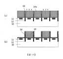
1.第1實施形態(固態攝影元件的構成)針對本發明第1實施形態的固態攝影元件的構成,使用圖1及圖2作說明。如圖1所示,本實施形態的固態攝影元件1具備半導體基板10、配置在半導體基板10上方的複數個微透鏡200、以及設置在半導體基板10與微透鏡200之間的濾色器100及分隔壁50。又,在微透鏡200之上形成有微透鏡平坦化層300。半導體基板10係具有二維地、亦即平面圖中配置成矩陣狀的複數個光電轉換元件11、及以使在各光電轉換元件11間轉換的電子不會混合之方式設置在光電轉換元件11間的元件分離構造12。1. The first embodiment(Constitution of solid-state imaging device)The structure of the solid-state imaging element according to the first embodiment of the present invention will be described with reference to FIGS. 1 and 2.As shown in FIG. 1, the solid-
微透鏡200係以複數個微透鏡層所形成。具體言之,微透鏡200係以和光電轉換元件11最接近地設置(亦即,設置在最下部)的第1微透鏡層20、及其上部所形成的第2微透鏡層21所構成。濾色器100係以複數色的濾色器所構成。具體言之,濾色器100係以第1濾色器14、第2濾色器15及第3濾色器16按既定的規則圖案配置所構成。分隔壁50係形成在第1濾色器14、第2濾色器15及第3濾色器16各個之間。分隔壁50係以內側的分隔壁30與將分隔壁30保護地覆蓋的分隔壁31兩層所形成。The
圖1雖圖示出在微透鏡200上部存在有微透鏡平坦化層300的構成,但亦可因固態攝影元件1的構成而不存在。又,分隔壁50雖顯示分隔壁30及分隔壁31兩層的構成,但依固態攝影元件1的構成而異,可為1層的構成,亦可為2層以上的構成。又,分隔壁50的高度可低於濾色器100,亦可比其還高。又,固態攝影元件1的畫素尺寸大的情況,也可以沒有分隔壁50。Although FIG. 1 illustrates a configuration in which the
以下,在說明本實施形態的固態攝影元件1時,將在濾色器100的製造步驟上最先形成且在濾色器100中占有面積最廣的濾色器定義成第1濾色器14。又,將在濾色器100的製造步驟上第二個形成的濾色器定義成第2濾色器15、和將在濾色器100的製造步驟上第三個形成的濾色器定義成第3濾色器16。在其他的實施形態亦是相同。又,以下的說明中係假想第1濾色器14是綠色時來作說明,但是第1濾色器14也可以是藍色或紅色。以下,針對固態攝影元件1的各構成要素作詳細說明。Hereinafter, when describing the solid-
(光電轉換元件及半導體基板)如圖1所示,於依據本實施形態的固態攝影元件1中的半導體基板10,複數個光電轉換元件11與畫素位置對應地呈二維配置。光電轉換元件11的每一者具有將光轉換成電氣信號的機能。又複數個光電轉換元件11的每一者係形成有元件分離構造12,使得光在被光電轉換元件11吸收前進入鄰接的光電轉換元件11或經光電轉換的電子不會流通於鄰接的其他光電轉換元件11的電路。作為元件分離的方法,雖可採用摻雜元件分離區域的半導體基板10、形成空隙或者埋入金屬或氧化物、氮化物、介電體等的方法等各式各樣的構成,但宜為光或電子難以在鄰接的其他光電轉換元件11的電路流動的構造。一般而言,係在藉由蝕刻將光電轉換元件11間的半導體基板10挖掘後,將金屬或氧化物、介電體等堆積而形成。形成有光電轉換元件11的半導體基板10,通常以表面(光射入面)的保護及平坦化為目的而在最表面形成有保護膜。半導體基板10係由能供可見光透射且能耐至少300℃左右的溫度之材料所形成。此處,作為使用於半導體基板10的耐熱材料,例如,可例舉出Si、SiO2等之氧化物及SiN等之氮化物,以及此等的混合物等之含有Si的材料等。此時,光電轉換元件11係配合後述的微透鏡200的材料、高度等而配置在可受光射入的光之位置。(Photoelectric conversion element and semiconductor substrate) As shown in FIG. 1, in the
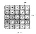
(濾色器及分隔壁)藉既定的圖案構成濾色器100之第1濾色器14、第2濾色器15及第3濾色器16(第1、第2及第3濾色器的一例)係對射入光進行彩色分離(Color separation)之和各色(綠、藍及紅)對應的濾色器。如圖1所示,第1濾色器14、第2濾色器15及第3濾色器16係設在半導體基板10與微透鏡200之間,且和複數個光電轉換元件11每一者對應的方式以因應於畫素位置而預設的規則圖案配置。(Color filter and partition wall)The
圖2係顯示第1濾色器14、第2濾色器15及第3濾色器16及在構成濾色器100的各濾色器之間所形成之分隔壁50的排列之平面圖。圖2所示之排列為所謂的拜耳排列,係鋪滿第1濾色器14、第2濾色器15及第3濾色器16的排列。此外,固態攝影元件1的各濾色器(第1濾色器14、第2濾色器15及第3濾色器16)未必限定拜耳排列,又,各濾色器的顏色亦未受限於紅(R)、綠(G)、藍(B)3色。又,亦可在濾色器100的排列的一部分配置已調整折射率之透明的層或能將可見光遮光且供紅外線透射的層(亦即紅外線用等之濾色器)。又亦可將鄰接的4個畫素設為同色且以16個畫素作拜耳排列之方式使用複數畫素作配置。2 is a plan view showing the arrangement of the
構成濾色器100之各濾色器含有既定色的顏料(著色劑)與熱硬化成分或光硬化成分。例如,第1濾色器14係含有作為著色劑的綠色顏料,第2濾色器15係含有藍色顏料,第3濾色器16係含有紅色顏料。Each color filter constituting the
分隔壁50係建構在構成濾色器100之複數色的濾色器(第1濾色器14、第2濾色器15及第3濾色器16)的各自之間。本實施形態中,藉由設於第1濾色器14的側壁部(外周圍)之分隔壁50,可將第1濾色器14、第2濾色器15及第3濾色器16各自分隔。圖1示出分隔壁50作成2層的構成,如圖1所示在內側形成分隔壁30,且分隔壁31形成覆蓋其外側及半導體基板10。The
內側的分隔壁30較佳為以遮光性高且能藉蝕刻等精度佳地微細加工的金屬材料,例如鎢(W)、鋁(Al)、銅(Cu)的膜所形成。又再者,亦可使用下層以鎢形成且上層使用鈦等之複數個金屬膜的積層構造。又亦可不為此等金屬的單體而為使用化合物。The
分隔壁31係覆蓋分隔壁30的外側,且使用SiO2、SiN、SiON等之氧化物、氮化物等並使用比濾色器低的折射率材料以如光波導管可引導光的構成來形成。又在該分隔壁31成為分隔壁30的保護膜且於分隔壁30使用金屬的情況,可抑制金屬的反應。分隔壁內側的分隔壁30也可使用金屬和氧化物、氮化物等之複數個材料來形成。較佳為以將進入相鄰的濾色器的光遮光、反射且作為光波導管之構成的材料所形成。The
分隔壁50的高度宜為可獲得所期望的分光特性之各濾色器的膜厚同等者。分隔壁50的高度高於濾色器的情況,後述的微透鏡200的膜厚薄的谷部與分隔壁50之配置在光電轉換元件11的中心部分容易重疊。因此,無法以微透鏡聚光的光從分隔壁50上部射入且通過外側的分隔壁31並在未分光下進入光電轉換元件11的機率上升。另外濾色器100的膜厚在各濾色器間全設為相同膜厚有困難,因此構成為有同等膜厚但具有厚度上的差異。具體言之,宜為從比膜厚最厚的濾色器厚上50nm左右到是膜厚最厚的濾色器的膜厚之一半左右。在依固態攝影元件1的構造而可抑制混色的情況,係即使是濾色器100的膜厚的一半以下的高度也沒有問題。因為在分隔壁50的高度低於濾色器100的情況,由於分隔壁50上部形成有濾色器100,在前述未被分光地從分隔壁50上部射入的光會減低。分隔壁50的橫方向的寬度係在將光遮光、反射且成為光波導管的範圍下越薄越好。因為越薄越能加大光電轉換元件11的開口面積,且能抑制從前述的分隔壁50上部進入的光。具體言之,分隔壁50的寬度宜為100nm以下,更宜為50nm以下。The height of the
分隔壁50,通常宜為比濾色器100還先形成於半導體基板10。藉由先形成分隔壁50而在格柵上作成有溝的場所形成各濾色器。習知構造的濾色器之形成方法為,在平坦的面上使濾色器具感光性並選擇性曝光顯影而形成矩形的圖案。在進行畫素圖案的微細化之情況,各濾色器的膜厚係成為薄膜的傾向。因此,在以薄膜形成所期望的顏色之情況,具有必須增大顏料等之著色成分的含有量,而感光性成分的含有量變少的結果,圖案化變困難的問題。但是,在既已設置分隔壁50且於其格柵上的溝部填孔以形成各濾色器的情況,只要選擇性曝光的部分夠硬即可。因此,具有上述的圖案化之難易度降低,即使感光性成分的含有量少亦可,濾色器材料的作成難易度變容易的優點。The
(微透鏡)固態攝影元件1中的微透鏡200,係於半導體基板10上方,配置在與畫素位置對應的位置。亦即,微透鏡200係複數個透鏡分別設置在複數個光電轉換元件11各自對應的位置。微透鏡200係藉由使射入微透鏡200的射入光聚光於光電轉換元件11的每一者上,可彌補光電轉換元件11的靈敏度降低。本發明的微透鏡200係如圖1所示以複數個微透鏡層形成。又,較佳為最接近光電轉換元件11的下層所設置的第1微透鏡層20製作微透鏡形狀,第2微透鏡層21以後的複數個微透鏡層被形成在第1微透鏡層20的透鏡面上的構成。本實施形態中,微透鏡200是以第1微透鏡層20與第2微透鏡層21兩層所形成。(Micro lens)The
為了以微透鏡200使聚光效率提升,第1微透鏡層20較佳為高折射率材料。具體言之較佳為折射率1.75以上2.15以下的範圍。在折射率為2.15以上的材料之情況,微透鏡200的聚光能力雖會提升,但因與濾色器100的折射率差變大使得在微透鏡200與濾色器100之界面等的反射光增加而有聚光效率降低的情況。在微透鏡的習知構造中,一般於微透鏡200使用有機系樹脂的材料,有機系樹脂中即使為高折射率材料亦是1.7以下程度。又,當使用折射率高的有機系材料時,有透射率易降低的傾向。In order to improve the light collection efficiency with the
在使用微細的固態攝影元件1之一般的相機模組之情況,微透鏡200之會有光射來的外側係和折射率接近1的空氣接觸。微透鏡200的折射率為1.75以上的情況,基於微透鏡200的聚光能力雖會提升,但因為在微透鏡200與空氣之間的折射率差大,所以變得容易引起光之反射。在該情況,有可能射入微透鏡200內部的光減少,招致受光靈敏度之降低。In the case of a general camera module using a fine solid-
折射率高且從380nm到700nm的可見光之透射率高的無機材料,可想到氮化矽(折射率:約2.0)、氧化鋯(折射率:約2.2)、氧化鈦(折射率:約2.49)、硫化鋅(折射率:約2.35)、氧化鋅(折射率:約2.01)、氧化鉿(折射率:約1.91)、氮化鋁(折射率:約2.16)、氧化鉭(折射率:約2.16)等。在形成微透鏡200的情況,因為設於下層的濾色器100的耐熱性一般為300℃以下,故較佳為以該溫度以下所形成的材料。形成微透鏡200的材料係能用300℃以下的溫度形成,用乾蝕刻等之公知方法進行形狀加工是容易的,而若是後述的消光係數低的材料的話什麼材料都沒問題,但當考慮因形成溫度或前述的折射率差所致之反射時,較佳為無機材料是使用氮化矽。藉由無機材料是使用透明且呈現高折射率的氮化矽,第1微透鏡層20係成為高折射率的微透鏡。因為第1微透鏡層20呈現高的折射率,即便將第1微透鏡層20的高度形成比習知者還低,亦能使射入光分別射入與各透鏡對應設置的畫素。又,因為第1微透鏡層20的高度可形成比習知還低,所以應射入鄰接的畫素之射入光被第1微透鏡層20所阻斷,可抑制固態攝影元件1整體之受光效率降低。因此,在無損及在各色的靈敏度特性之下,可提供呈現聚光特性的固態攝影元件1。Inorganic materials with high refractive index and high transmittance of visible light from 380nm to 700nm include silicon nitride (refractive index: about 2.0), zirconium oxide (refractive index: about 2.2), and titanium oxide (refractive index: about 2.49) , Zinc sulfide (refractive index: about 2.35), zinc oxide (refractive index: about 2.01), hafnium oxide (refractive index: about 1.91), aluminum nitride (refractive index: about 2.16), tantalum oxide (refractive index: about 2.16) )Wait. In the case of forming the
氮化矽(Si3N4)的折射率為2.0左右,但矽與氮之比例依成膜條件而變化,折射率係從1.7變化到2.1左右。又,在將氮化矽用作微透鏡200的材料之情況必須透射率為高者。透射率係依材質的膜厚而變化,故而在指標方面能以光學常數的消光係數來表示。發明者們的知識見解為消光係數在使用於微透鏡的材料上是重要的。折射率與消光係數呈現因成膜條件而異。在固態攝影元件1所使用的氮化矽多為使用CVD(Chemical Vapor Deposition)所形成。使用CVD形成時的成膜條件之品質依溫度、壓力、氣體種類及氣體流量等之控制而異。以下層的濾色器100之耐熱溫度300℃以下形成的情況,藉由在上述條件下使用電漿源且使用在低壓環境下能採用低溫工序的電漿CVD(電漿增強化學氣相沉積;Plasma-enhanced Chemical Vapor Deposition),容易形成品質良好的氮化矽。在氮化矽的折射率高的成膜條件下消光係數易變不佳,折射率與消光係數雙方優異的成膜條件的情況係條件的範圍狹窄,膜所內含的應力易變高。應力高的情況,有不適合於在濾色器100上形成微透鏡200時的傾向。因此,作為適合於微透鏡200的氮化矽膜,較佳為折射率為1.75以上2.0以下且在380nm以上700nm以下的可見光之範圍下的消光係數為1.0×10⁻³以下。再者,作為適合於微透鏡200的氮化矽膜,最好為折射率為1.85以上2.0以下且在波長300nm以上700nm以下的範圍的消光係數為1.0×10⁻³以下的膜質。The refractive index of silicon nitride (Si3 N4 ) is about 2.0, but the ratio of silicon to nitrogen varies depending on the film forming conditions, and the refractive index varies from 1.7 to about 2.1. In addition, when silicon nitride is used as the material of the
前述的條件雖是形成氮化矽膜的情況,但藉由在用電漿CVD形成時併用含氧的N2O氣體等,可形成氮氧化矽(組成式SiON)膜。氮氧化矽膜係藉由氧的含有量可形成從氮化矽(折射率:2.0)到氧化矽(折射率:1.45)的折射率,消光係數也容易控制。因此,亦可將氮氧化矽使用於第1微透鏡層20。Although the aforementioned conditions are for the formation of a silicon nitride film, a silicon oxynitride (compositional SiON) film can be formedby using an oxygen-containing N 2 O gas or the like in the formation by plasma CVD. The silicon oxynitride film can form a refractive index from silicon nitride (refractive index: 2.0) to silicon oxide (refractive index: 1.45) due to the oxygen content, and the extinction coefficient is also easy to control. Therefore, silicon oxynitride can also be used for the
作為第1微透鏡層20的形成方法,在濾色器100上以各種成膜條件形成高折射的第1層。作為第1層,較佳為以電漿CVD形成前述的氮化矽層的方法。其次,形成用以形成後述的透鏡基質之屬於第2層的中間犧牲層。中間犧牲層係利用樹脂材料所形成,使用例如未具有熱流性的感光性樹脂。藉此,可回避因熱流使感光性樹脂圖案熔融,體積膨脹造成鄰接的透鏡彼此接觸的情形。其結果,可防止在相鄰的透鏡彼此的交界部分發生形狀崩塌的情形。此處,在形成透鏡基質方面,可採用的不因熱而流動的感光性樹脂,以玻璃轉移溫度高、且依100~220℃的條件之熱處理在硬化前形狀不崩塌的熱塑性之樹脂材料是適合的。作為此種不因熱而流動感光性樹脂,較佳為含有質量平均分子量(Mw:依據凝膠滲透層析術(gel permeation chromatography;GPC)的苯乙烯轉化的測定値)為10,000以上30,000以下的基底樹脂。更佳為,質量平均分子量為20,000以上30,000以下。藉由基底樹脂的質量平均分子量為10,000以上而提升耐熱性、耐熱流性。又,藉由基底樹脂的質量平均分子量設為30,000以下,因顯影時的溶解性不會降低,所以可抑制殘渣之產生。As a method of forming the
接著,為了形成透鏡基質而將具有感光性的光阻劑形成於中間犧牲層上。藉由將該光阻劑選擇性地曝光顯影而在將形成微透鏡的場所形成光阻劑,再以該光阻劑的形狀會崩塌的溫度條件進行加熱烘烤,使阻劑形狀因熱流動形成透鏡形狀的阻劑。其次,以透鏡形狀的阻劑為遮罩對中間犧牲層全面進行乾蝕刻,藉由以正型的阻劑全部的量消失的時間設定進行蝕刻,形成在中間犧牲層轉印了透鏡形狀的透鏡基質。接著,以透鏡基質為遮罩對第1層全面進行乾蝕刻,在第1層轉印透鏡基質的形狀而形成第1微透鏡層20。微透鏡的透鏡形成方法除了使用前述之阻劑的熱流法之方法外也能使用公知的方法。例如,以使用灰階圖案的光罩,藉由調整曝光量,於顯影後直接成為透鏡形狀之方式形成亦可。因為在使用任一種方法都難以將第1微透鏡層20直接形成透鏡形狀,所以適合的方法為,在形成平坦的第1微透鏡層20上使用在之後會被除去的犧牲層製作出透鏡形狀,再將其形狀藉由公知的蝕刻方法轉印到第1微透鏡層20。Next, in order to form a lens matrix, a photosensitive photoresist is formed on the intermediate sacrificial layer. By selectively exposing and developing the photoresist, the photoresist is formed in the place where the microlenses will be formed, and then the photoresist is heated and baked at a temperature condition where the shape of the photoresist will collapse, so that the shape of the resist flows due to heat Form a resist in the shape of a lens. Next, dry etching is performed on the entire surface of the intermediate sacrificial layer with a lens-shaped resist as a mask, and etching is performed with the time setting when the entire amount of the positive type resist disappears, and a lens with the lens shape transferred to the intermediate sacrificial layer is formed. Matrix. Next, the entire surface of the first layer is dry-etched using the lens substrate as a mask, and the shape of the lens substrate is transferred to the first layer to form the
此時,第1微透鏡層20的高度方向的膜厚為150nm以上400nm以下。此外,「第1微透鏡層20的高度方向的膜厚」,意指從半圓形狀透鏡的底面(第1實施形態中的濾色器100的上面)到第1微透鏡層20的透鏡頂點為止的高度。在各光電轉換元件11的間距(亦即第1微透鏡層20所具有的複數個透鏡之間距)為1.0μm以下的微細構造之情況,第1微透鏡層20的高度方向的膜厚只要為膜厚150nm以上400nm即可,更佳為150nm以上300nm。在微細的畫素圖案中,當將第1微透鏡層20的高度方向的膜厚設大時,應射入鄰接的畫素之射入光被第1微透鏡層20阻斷,具有固態攝影元件1的受光效率(受光靈敏度;Responsivity)降低的問題。又,當在微透鏡200形成部位的面積狹窄的條件下將第1微透鏡層20的膜厚(透鏡高度)設厚時,與透鏡的谷部對應之部分的膜厚變厚,亦有透鏡形狀崩塌導致形成光混色的區域之問題。然而,藉由將膜厚範圍設為上述範圍,可抑制此等問題,可提供呈現高聚光特性的固態攝影元件1。又,因為藉由將第1微透鏡層20的高度設低可將聚光點的位置置於濾色器100,所以靈敏度特性變好。特別是,藉由將第1微透鏡層20的高度設為150nm以上300nm以下的範圍,可在綠(G)、藍(B)、紅(R)的所有色中獲得良好的靈敏度特性。At this time, the film thickness in the height direction of the
微透鏡200的第2微透鏡層21係減低基於第1微透鏡層20的反射之層。如同前述,在第1微透鏡層20的折射率為1.75以上2.15以下程度的情況,因為折射率低的空氣處於外側,故在第1微透鏡層20表面之反射多,易引起靈敏度降低。因此,在以複數個層所構成的微透鏡200的第2以後的層,係控制折射率並形成為防反射層。亦即,藉由在第1微透鏡層20的透鏡面上設置第2微透鏡層21,可防止損及固態攝影元件1的靈敏度特性。因此,第2微透鏡層21的折射率較佳為比第1微透鏡層20的折射率還低,較佳為例如1.4以上1.75以下。在使用折射率為1.75以上的材料之情況,在第1微透鏡層20的透鏡表面(第1微透鏡層20與第2微透鏡層21之交界)之射入光的反射多,在固態攝影元件1易引起靈敏度降低。特別是,畫素一經微細化就容易發現上述的反射光。因此,藉由將第2微透鏡層21的折射率設為1.4以上1.75以下,可提供能抑制反射光之微細的固態攝影元件1。本實施例中,微透鏡200係示出以2層構成的情況,作為第2微透鏡層21,氧化矽(SiO2)或氧量多的氮氧化矽(SiON)是適合的。亦即,第2微透鏡層21較佳為氧含有量比第1微透鏡層20還高。使用氧化矽的情況,除了電漿CVD等之氣相成膜方法以外,亦可使用SOG(Spin On Glass;旋轉塗布玻璃)或矽氧烷等之塗布型的材料來形成。只要為能以位在前述下層的濾色器之耐熱溫度300℃以下形成的方法,則亦可使用公知的任何方法。The
第2微透鏡層21的膜厚若可形成薄,則適合較薄者。具體言之,第2微透鏡層21的膜厚較佳為5nm以上2000nm以下,更佳為10nm以上200nm以下,再更佳為50nm以上150nm以下。又,第2微透鏡層21的膜厚T2對上述的第1微透鏡層20的膜厚T1之比率(T2/T1)較佳為0.125以上1.0以下。If the film thickness of the
(微透鏡平坦化層)本實施形態中,示出於微透鏡200在上部(光射入方向),形成有設於微透鏡200的透鏡面上且上面形成平坦的微透鏡平坦化層300之構造。一般的固態攝影元件之情況,微透鏡200的外側為空氣層,作為相機模組構造,在其上部形成聚光透鏡或紅外線截止板等之模組構造。在本實施形態所示那種一個畫素尺寸成為1μm以下那樣的已微細化的固態攝影元件1之情況,微透鏡200的構造亦同樣地被微細化,成為構成微透鏡200之各透鏡的間隔成為接近於光的波長之構成。因此,微透鏡的構造自體很可能如菲涅耳透鏡或繞射透鏡般成為對射入的光帶來影響之構造。因此,即便是如前者所示空氣層在平時是位在外側那種一般的固態攝影元件之情況,在微透鏡200上部形成微透鏡平坦化層300是適合的。(Micro lens flattening layer)In this embodiment, the
作為微透鏡平坦化層300的材料,可想到有機材料或無機材料,宜為經考慮折射率的材料。在微透鏡200的上方為空氣那樣的一般模組之情況,宜為在空氣與作為微透鏡200的表面的第2微透鏡層21的折射率之間的材料。具體言之較佳為折射率1.1以上1.6以下程度的折射率,更佳為1.20以上1.45以下。宜為是該範圍的折射率且為相對於可見光是透射率高的材料。藉此,抑制經由微透鏡平坦化層300射入的光在微透鏡200表面反射的情況,可提升聚光特性、靈敏度特性並獲得微細的固態攝影元件。又,膜厚雖然100nm以上100μm以下程度沒有特別限制,但宜為可將微透鏡200平坦化的膜厚。作為低折射率材料,透過在有機系樹脂含有矽氧烷系聚合物、二氧化矽、氟聚合物等作為無機聚合物,或透過使之含有中空填料,可形成折射率1.6以下。不受上述的方法所限,只要是透明性高且能作成平坦的材料之組合就沒有問題。As the material of the
<第1實施形態的效果>本實施形態中,在濾色器100之上形成有微透鏡200。微透鏡200係於第1微透鏡層20之上形成有第2微透鏡層21。第1微透鏡層20的膜厚(從透鏡底面到透鏡頂點為止的高度)係150nm以上400nm以下。藉由此等構成,藉由折射率高的微透鏡使聚光能力高,藉由從複數個層形成的微透鏡200可減低在微透鏡部分之反射。又藉由設定第1微透鏡層20的高度,可利用所有濾色器形成高靈敏度。<Effects of the first embodiment>In this embodiment, a
本實施形態中,僅基於一般的光電轉換元件之構成作描述,近年來,亦有為了焦點檢測而改變光電轉換元件部的一部分構造以形成像面相位差對焦(Phase Detection AF)的構造。使用攝像元件內的複數個焦點檢測畫素從信號求得偏移量,算出焦點的修正量。在那樣構造的情況,有時在攝像元件內改變一部分排列或將複數個畫素以一個畫素形成。像面相位差對焦的畫素有1畫素份、2畫素份、4畫素份等之各式各樣的構成,但在該情況,和光電轉換元件對應的濾色器或微透鏡未必與光電轉換元件成為一對。例如,相對於光電轉換元件為複數時,濾色器及微透鏡為1個,或相對於光電轉換元件與濾色器為複數時,微透鏡為1個的構成。又,配合此等的構成而形成分隔壁50。即便是形成有此種像面相位差對焦的固態攝影元件之情況,本實施形態亦可適用,該部分的微透鏡和光電轉換元件未必成為一對,僅形狀稍不同,這以外的部分和實施形態相同。In this embodiment, the description is based only on the structure of a general photoelectric conversion element. In recent years, there has also been a structure in which a part of the photoelectric conversion element portion is changed for focus detection to form phase detection AF (Phase Detection AF). A plurality of focus detection pixels in the imaging element are used to obtain the offset amount from the signal, and calculate the focus correction amount. In the case of such a structure, a part of the arrangement in the imaging element is changed or a plurality of pixels are formed by one pixel. The image plane phase difference focusing pixels have various configurations such as 1-pixel, 2-pixel, 4-pixel, etc. However, in this case, the color filter or microlens corresponding to the photoelectric conversion element is not necessarily It becomes a pair with the photoelectric conversion element. For example, when the photoelectric conversion element is plural, the color filter and the microlens are one, or when the photoelectric conversion element and the color filter are plural, the microlens is one configuration. In addition, the
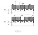
2.第2實施形態其次,針對本發明第2實施形態,使用圖3作說明。如圖3所示,本實施形態的固態攝影元件2與第1實施形態的固態攝影元件1的不同點為,在濾色器100與微透鏡200之間形成濾色器平坦化層40,以將濾色器100的凹凸平坦化並緩和微透鏡200形成時之應力。2. The second embodimentNext, the second embodiment of the present invention will be described with reference to FIG. 3. As shown in FIG. 3, the solid-
以下,針對固態攝影元件2的構成,記載和第1實施形態中的固態攝影元件1的製造方法不同的部分。Hereinafter, regarding the configuration of the solid-
(濾色器平坦化層)濾色器平坦化層40被形成在半導體基板10上所形成的濾色器100及分隔壁50的上面。濾色器平坦化層40的膜厚係形成可將由形成濾色器100的各濾色器(第1濾色器14、第2濾色器15、第3濾色器16)與分隔壁50所形成的階差平坦化的膜厚。又,在濾色器平坦化層40的上部形成第1微透鏡層20,但以無機材料形成第1微透鏡層20,形成折射率高且消光係數低的微透鏡之情況,帶有應力地形成微透鏡的可能性容易變高。在微透鏡200所內含的應力大的情況,於烘烤步驟等之後加熱步驟已進行時,有時會因為下層的濾色器100與微透鏡200的熱膨脹係數不同而發生裂紋、透鏡與濾色器位置偏移等之問題。濾色器平坦化層40可緩和此種應力的偏移。又,在形成第1微透鏡層20時,以重視折射率或消光係數的條件下成膜的情況,有時平坦性差而順應圖案的凹凸被成膜,有在與濾色器100之間產生間隙的情況。然而,因在第1微透鏡層20下層形成濾色器平坦化層40,掩埋濾色器平坦化層40與濾色器100之間的間隙,可防止靈敏度特性之劣化。(Color filter flattening layer)The color
本實施形態中,微透鏡200的折射率為1.75以上2.15以下,各濾色器的折射率雖按各色而異,一般為1.4以上1.7以下程度。因此,當濾色器100與微透鏡200之間形成有折射率大不相同的材料時,在界面容易引起反射,有可能發生靈敏度降低。因此,濾色器平坦化層40的折射率較佳為1.6以上1.8以下,更佳為1.6以上1.7以下。在濾色器平坦化層40的折射率為1.6以上1.8以下的情況,可縮小與第1微透鏡層20的折射率之差使聚光特性提升。又,構成濾色器平坦化層40之材料係難以被施加來自有機樹脂等之應力的材料,較佳為相對於波長380nm以上700nm以下的可見光呈透明且透射率高的材料。In this embodiment, the refractive index of the
作為濾色器平坦化層40的材料,藉由含有例如丙烯酸系樹脂、環氧系樹脂、聚醯亞胺系樹脂、酚醛清漆系樹脂、聚酯系樹脂、胺基甲酸酯系樹脂、三聚氰胺系樹脂、尿素系樹脂、苯乙烯系樹脂及矽系樹脂等中的一或複數樹脂所形成。又濾色器平坦化層40,除了有機化合物以外,亦能以含有例如矽、碳、氧、氫、錫、鋅、銦、鋁、鎵、鈦、鉬、鎢、鈮、鉭、鉿、銀及氟之中至少1種的化合物、氧化化合物或氮化化合物所形成。作為此等材料的化合物,可使用例如ITO或ZnO、TiO2、HfO2等。又,濾色器平坦化層40係藉由此等材料形成單層或多層。本實施形態中,亦能藉由在濾色器平坦化層40使用有機系樹脂來形成。又作為濾色器平坦化層40的材料,亦能藉由以氮氧化矽增加氧的比例而形成,調整折射率形成為平坦化層。As the material of the color
濾色器平坦化層40的膜厚較佳為10nm以上300nm以下之範圍的膜厚。又,從固態攝影元件2的微細化及抑制混色的觀點,較佳為濾色器平坦化層40較薄者,更佳為濾色器平坦化層40的膜厚為10nm以上150nm以下。又,本實施形態的濾色器平坦化層40亦有緩和應力或熱膨脹係數之差的目的,在達成該目的之範圍較佳為薄膜。The film thickness of the color
在將上述那樣形成的濾色器100平坦化的濾色器平坦化層40上形成有第1微透鏡層20。將第1微透鏡層20以無機材料形成的情況,就提高折射率且使消光係數接近0的條件而言,容易內含應力。和第1實施形態同樣地,在第1微透鏡層20使用氮化矽(SiN)的情況,該傾向變得顯著。第1實施形態中,因為要在下層的濾色器100上直接形成第1微透鏡層20,所以必須減低應力來形成,可採取的形成條件之範圍有變窄的傾向。本實施形態中,因為在第1微透鏡層20下層設置濾色器平坦化層40,所以具有擴大第1微透鏡的形成條件的範圍之優點。The
本實施形態中,第1微透鏡層20的高度(從濾色器平坦化層40上面到第1微透鏡層20頂點為止的高度)較佳為150nm到400nm程度。In this embodiment, the height of the first microlens layer 20 (the height from the upper surface of the color
<變形例>以下,針對本發明第2實施形態的變形例,使用圖4作說明。如圖3所示,本實施形態的固態攝影元件2雖具有微透鏡平坦化層300,但未受限於此種構成。例如,如圖4所示,第2實施形態的變形例之固態攝影元件2A具備半導體基板10、濾色器100、濾色器平坦化層40、微透鏡200、及分隔壁50。亦即,在沒有微透鏡平坦化層300這點是和第2實施形態的固態攝影元件2相異。此外,半導體基板10、濾色器100、濾色器平坦化層40、微透鏡200及分隔壁50因為是和在第1實施形態及第2實施形態說明過的各部分相同的構成,故省略說明。<Modifications>Hereinafter, a modification of the second embodiment of the present invention will be described with reference to FIG. 4. As shown in FIG. 3, although the solid-
<第2實施形態的效果>本實施形態的固態攝影元件2中,在濾色器100與微透鏡200之間,設有濾色器平坦化層40。因此,濾色器平坦化層40緩和來自其他層的應力,且可使微透鏡200的下面平坦,可適當形成微透鏡200。又,就本實施形態的固態攝影元件2而言,具有擴大第1微透鏡層20之形成條件的範圍之優點。具體言之,具有在使用電漿CVD等之成膜裝置時可提高成膜溫度的優點。無機材料等因為會有內含的應力等依成膜溫度而變化的傾向,故如上述可獲得濾色器平坦化層40緩和應力等之效果。因此,即便成膜溫度比設定溫度還稍有變動,仍可獲得在品質上不發生問題的效果。<Effects of the second embodiment>In the solid-
3.第3實施形態其次,針對本發明第3實施形態,使用圖5作說明。如圖5所示,本實施形態的固態攝影元件3係在微透鏡200具有設於第2微透鏡層21的上面之第3微透鏡層22這點和第1實施形態的固態攝影元件1相異。3. The third embodimentNext, the third embodiment of the present invention will be described with reference to FIG. 5. As shown in FIG. 5, the solid-
以下,針對固態攝影元件3的構成,記載與第1實施形態中的固態攝影元件1的製造方法不同的部分。Hereinafter, regarding the configuration of the solid-
(微透鏡)微透鏡200具有第1微透鏡層20、第2微透鏡層21、第3微透鏡層22。第1微透鏡層20及第2微透鏡層21係與第1實施形態的固態攝影元件1的第1微透鏡層20及第2微透鏡層21相同。第3微透鏡層22係減低因第1微透鏡層20所致之反射的層,具有比第2微透鏡層21還低的折射率。第3微透鏡層22較佳為氧含有量比第2微透鏡層21還高。(Micro lens)The
本實施形態中,雖示出微透鏡200係以3層所形成的構成,但只要是折射率從接近於光電轉換元件11的下層越往上層變越低的傾向,則多少層都沒有問題。又,在本實施形態中,和第1實施形態同樣地,雖示出在濾色器100與微透鏡200之間沒有濾色器平坦化層40的構成,但也可設有濾色器平坦化層40。In this embodiment, although the
(微透鏡之形成方法)迄至第1微透鏡層20的形成步驟為止係和第1實施形態相同。接下來,形成第2微透鏡層21。第二微透鏡係在折射率為1.5~1.75的範圍形成。接著,形成第3微透鏡層22。第3微透鏡層22係在折射率為1.3以上1.5以下形成。透過伴隨著從微透鏡的內側進到外側階段地降低折射率,縮小與空氣的折射率差,以減低在微透鏡的表面之反射。(Method of forming micro lens)The steps up to the formation of the
第2以後的微透鏡可一層一層形成,亦可連續地形成。使用例如用電漿CVD形成的氮氧化矽,藉由以初期氮化物的比例多的條件形成且中途變為氧化物多的條件之方式變化氣體的流量等,來控制折射率亦可。The second and subsequent microlenses may be formed layer by layer, or may be formed continuously. For example, silicon oxynitride formed by plasma CVD may be used, and the refractive index may be controlled by changing the flow rate of the gas so that it is formed under a condition where the ratio of initial nitride is high and becomes a condition where there is much oxide in the middle.
又,藉由將第3微透鏡層22的膜厚設厚可變化折射率及微透鏡的形狀。藉由將微透鏡平坦化,省略後續步驟的微透鏡平坦化層300亦可使步驟容易。In addition, the refractive index and the shape of the microlens can be changed by setting the thickness of the
使用第2以後的微透鏡賦予微透鏡平坦化層300的效果之情況,係亦可使用例如折射率1.2以上1.5以下程度的低折射率材料。When the second and subsequent microlenses are used to impart the effect of the
藉由使用第3實施形態,可控制微透鏡的折射率,成為可控制聚光能力。By using the third embodiment, the refractive index of the microlens can be controlled, and the light-gathering ability can be controlled.
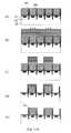
4.第4實施形態其次,針對本發明第4實施形態,使用圖6至圖8作說明。圖6表示本實施形態的固態攝影元件4的一構成例之平面圖。固態攝影元件4至少具備半導體基板10、濾色器100、微透鏡200A、及分隔壁50。固態攝影元件4係在取代微透鏡200而改為具備微透鏡200A這點與第1實施形態~第3實施形態的各固態攝影元件1~3相異。以下,針對微透鏡200A作詳細說明。此外,半導體基板10、濾色器100、濾色器平坦化層40及分隔壁50,因為是和在第1實施形態及第2實施形態說明過的各部分相同的構成故省略說明。4. Fourth EmbodimentNext, the fourth embodiment of the present invention will be described with reference to Figs. 6 to 8. FIG. 6 shows a plan view of a configuration example of the solid-state imaging element 4 of this embodiment. The solid-state imaging element 4 includes at least a
(微透鏡)微透鏡200A係和微透鏡200同樣地以複數(例如2層)的微透鏡層所形成。本實施形態中,針對微透鏡200A具備設在最接近於光電轉換元件11的下層之第1微透鏡層20A及設於第1微透鏡層20A的透鏡面上之第2微透鏡層21A的情況作說明。此外,第1微透鏡層20A及第2微透鏡層21A的剖面構成係和微透鏡200的第1微透鏡層20及第2微透鏡層21相同,在後述的圖6中,第1微透鏡層20A及第2微透鏡層21A未圖示出。(Micro lens)The
微透鏡200A係具有與複數個光電轉換元件11分別對應的複數個透鏡。如圖6所示,微透鏡200A為,鄰接的複數個透鏡在平面圖中接觸著。微透鏡200A中,鄰接的複數個透鏡在平面圖中呈線狀接觸,但未必一定是呈線狀接觸。又,微透鏡200A亦可為,在構成濾色器100之第1濾色器14、第2濾色器15及第3濾色器16各自的角部上具有間隙(gap),成為透鏡未覆蓋該角部上的形狀。又,微透鏡200A的填充因數(Fill Factor)較佳為80%以上100%以下,更佳為85%以上95%以下,該填充因數係表示透鏡覆蓋在具有光電轉換元件11的一個畫素上的比例。在填充因數為80%以上100%以下的情況,抑制因鄰接的透鏡間的間隙所致聚光特性之降低,綠(G)、藍(B)或紅(R)任一色的受光靈敏度皆提升,由於在85%以上95%以下受光靈敏度特別提升,故較佳。The
以下,參照圖7,針對填充因數作說明。圖7示意地顯示4個畫素及設置在各畫素P上的4個透鏡之平面構成的平面圖。填充因數係由以下式(1)所規定。填充因數[%]={1-(a×a)/(A×A)}×100 ・・・(1)此處,A表示畫素尺寸,a表示在透鏡產生的間隙的對角線上之距離,且a<A。又,填充因數係表示透鏡覆蓋在一個畫素上的比例,最大成為100%。Hereinafter, referring to FIG. 7, the filling factor will be described. FIG. 7 schematically shows a plan view of the plane configuration of 4 pixels and 4 lenses arranged on each pixel P. The filling factor is defined by the following formula (1).Filling factor [%]={1-(a×a)/(A×A)}×100 ・・・(1)Here, A represents the pixel size, a represents the distance on the diagonal of the gap created by the lens, and a<A. In addition, the fill factor system represents the ratio of the lens covering one pixel, and the maximum is 100%.
以上那樣的微透鏡200A係可藉由使用隔著後述的透鏡基質來形成微透鏡的方法而形成。此外,如圖8所示,在未使用後述的透鏡基質下形成微透鏡(200’)的情況,各畫素P上的該微透鏡20’之鄰接的複數個透鏡彼此不接觸,複數個透鏡分別獨立地形成。在該情況,透鏡間的間隙G變大,難以使聚光效率提升。The above-mentioned
<第4實施形態的效果>本實施形態中,固態攝影元件4因具備具有填充因數較佳為80%以上100以下、更佳為85%以上95%以下的透鏡之微透鏡200A,可使聚光特性提升。因微透鏡200A所具有的間隙所致之靈敏度特性的影響係在將微透鏡200A(第1微透鏡層20)的透鏡高度低時受到影響。因此,在第1微透鏡層20的膜厚為150nm以上400nm以下的情況中,藉由縮小透鏡間的間隙,可提供微細且更高靈敏度的固態攝影元件4。[實施例]<Effects of the fourth embodiment>In this embodiment, the solid-state imaging element 4 includes a
以下,針對本發明的固態攝影元件及習知的固態攝影元件作具體說明。<實施例1>實施例1中,說明和上述的第1實施形態的固態攝影元件1(參照圖1)同樣的製造方法。Hereinafter, the solid-state imaging device of the present invention and the conventional solid-state imaging device will be specifically described.<Example 1>In Example 1, the same manufacturing method as that of the solid-state imaging element 1 (see FIG. 1) of the first embodiment described above will be described.
首先,如圖9(a)至圖9(c)所示,準備半導體基板10,其具備呈二維配置的光電轉換元件11且各光電轉換元件11之間藉由元件分離構造12而使元件分離(圖9(a))。作為半導體基板10,使用光電轉換元件11的圖案尺寸為1μm以下的微細物。First, as shown in FIGS. 9(a) to 9(c), a
(分隔壁之形成)其次,在該半導體基板10上形成分隔壁50(圖9(b)、圖9(c))。首先,藉由電漿CVD成膜350nm膜厚的鎢膜。其次,於鎢膜上,將正型阻劑(TDMR-AR:東京應化工業股份有限公司製)使用旋轉塗布以1000rpm的旋轉數旋轉塗布之後,以90℃進行1分鐘預烘烤。藉此,製作將屬於感光性樹脂遮罩材料層(蝕刻遮罩)的光阻劑塗布了1.5μm膜厚的試樣。該屬於感光性樹脂遮罩材料層的正型阻劑係因紫外線照射使得紫外線照射部分起化學反應而溶解成顯影液。(Formation of the dividing wall)Next, a
對該試樣進行隔介光罩執行曝光之光微影製程。曝光裝置係使用將i線波長使用於光源的曝光裝置。光微影製程中,對感光性樹脂遮罩材料層中之形成濾色器的部分照射紫外線。A photolithography process of exposure was performed on the sample with a dielectric mask. The exposure device uses an exposure device that uses the i-line wavelength as a light source. In the photolithography process, ultraviolet rays are irradiated to the part of the photosensitive resin mask material layer that forms the color filter.
其次,將2.38質量%的TMAH(四甲基氫氧化銨;tetramethylammonium hydroxide)用作顯影液進行顯影步驟,在形成濾色器的場所形成具有開口部的感光性樹脂遮罩層。在作為感光性樹脂遮罩材料層是使用正型阻劑的情況,以進行顯影後脫水烘烤(Dehydration Bake),進行屬於感光性樹脂遮罩材料層的光阻劑之硬化者居多。本次係在120℃的溫度下實施脫水烘烤。感光性樹脂遮罩層係形成1.5μm的膜厚。Next, 2.38% by mass of TMAH (tetramethylammonium hydroxide) is used as a developing solution for a developing step, and a photosensitive resin mask layer having openings is formed at the place where the color filter is formed. In the case where a positive resist is used as the photosensitive resin mask material layer, most people perform the curing of the photoresist belonging to the photosensitive resin mask material layer by performing dehydration bake after development. This time, dehydration and baking were carried out at a temperature of 120°C. The photosensitive resin mask layer has a thickness of 1.5 μm.
其次,以感光性樹脂遮罩層為遮罩進行乾蝕刻。此時,所使用的乾蝕刻裝置係使用平行平板方式的乾蝕刻裝置。又,以對基底的半導體基板10不造成影響之方式在中途進行蝕刻條件的變更且以多階段實施乾蝕刻。Next, dry etching is performed using the photosensitive resin mask layer as a mask. At this time, the dry etching device used was a dry etching device of a parallel flat plate method. In addition, the etching conditions are changed in the middle so as not to affect the
一開始,使用氣體種類為混合SF6、Ar兩種氣體而成的蝕刻氣體實施蝕刻。SF6的氣體流量設為50ml/min,Ar的氣體流量設為100ml/min。又,將此時的腔室內的壓力設為2Pa的壓力,RF電源設為1000W來實施。使用該條件,蝕刻從感光性樹脂遮罩層露出的鎢膜的總膜厚200nm中的相當於90%的180nm程度。於該階段,變更成下個蝕刻條件。其次,使用SF6、O2、Ar三種氣體混合的蝕刻氣體實施蝕刻。將SF6的氣體流量設為5ml/min、O2的氣體流量設為50ml/min及Ar的氣體流量設為100ml/min,將從感光性樹脂遮罩層露出的鎢膜全部蝕刻除去。At the beginning, the etching is performed using an etching gas that is a mixture of SF6 and Ar. The gas flow rate of SF6 is set to 50 ml/min, and the gas flow rate of Ar is set to 100 ml/min. In addition, the pressure in the chamber at this time was set to a pressure of 2 Pa, and the RF power supply was set to 1000 W. Using this condition, about 180 nm, which is equivalent to 90%, of the total film thickness of 200 nm of the tungsten film exposed from the photosensitive resin mask layer is etched. At this stage, change to the next etching condition. Secondly, etching is performed using an etching gas mixed with three gases ofSF 6 , O2, and Ar. The gas flow rate of SF6 was set to 5 ml/min,the gas flow rate of O 2 was set to 50 ml/min, and the gas flow rate of Ar was set to 100 ml/min, and all the tungsten film exposed from the photosensitive resin mask layer was etched and removed.
其次,進行除去作為蝕刻遮罩使用的感光性樹脂遮罩層。此時使用的方法係使用溶劑的方法,使用剝離液104(東京應化工業股份有限公司製)以噴霧洗淨裝置進行除去感光性樹脂遮罩層。其後,藉由氧電漿進行灰化,進行除去殘留中的感光性樹脂遮罩層。藉由此等步驟,在半導體基板上以格柵形狀形成具有鎢分隔壁構造之內側的膜厚(高度)350nm、寬度60nm的分隔壁30(圖9(b))。Next, the photosensitive resin mask layer used as an etching mask is removed. The method used at this time is a method using a solvent, and the photosensitive resin mask layer is removed with a spray cleaning device using the peeling solution 104 (manufactured by Tokyo Ohka Kogyo Co., Ltd.). After that, ashing is performed by oxygen plasma to remove the remaining photosensitive resin mask layer. Through these steps, a
其次,使用電漿CVD形成作為分隔壁31的SiO2膜。此時使用的SiO2之成膜條件係對鎢圖案(分隔壁30)使用在高度方向形成厚膜的條件。藉由分隔壁30和分隔壁31所形成的分隔壁50的高度為600nm(圖9(c))。Next, a SiO 2 film as the
(第1濾色器之形成)其次,進行形成第1濾色器14的第1濾色器形成步驟(圖10(a)、圖10(b))。首先,為了設置第1濾色器14,將含有綠(G)的顏料且具感光性的阻劑(以下,稱為綠色阻劑14a)塗布於半導體基板10的全面(圖10(a))。此時,亦可在綠色阻劑14a塗布前,對半導體基板10的全面施以用以提升密著性的疏水化表面處理(HMDS處理)。其次,在藉由光微影製程將綠色阻劑14a選擇性曝光後,進行顯影,形成和第1濾色器14形成位置對應之圖案的綠色濾色器。此時,作為綠色阻劑14a主成分的樹脂,使用已賦予感光性的丙烯酸系的樹脂。又,使用在綠色阻劑14a的顏料,分別在色指數(color index)為C.I.PG58、C.I.PY150,顏料濃度為60質量%。又,綠色濾色器的膜厚為600nm。(Formation of the first color filter)Next, the first color filter forming step of forming the
其次,為使綠色濾色器牢固地硬化,以熱板在230℃下進行6分鐘烘烤以進行硬化,形成第1濾色器14(圖10(b))。確認經該加熱步驟後,即使經過第3濾色器形成步驟等之步驟亦無第1濾色器14剝落或圖案崩塌等情況。Next, in order to harden the green color filter, it is cured by baking at 230°C for 6 minutes on a hot plate to form the first color filter 14 (FIG. 10(b)). It was confirmed that after this heating step, there was no peeling off or pattern collapse of the
(第2濾色器之形成)其次,進行形成第2濾色器15的第2濾色器形成步驟(圖11(a)、圖11(b))。為了設置第2濾色器15,將含有藍(B)的顏料且具感光性的阻劑(以下,稱為藍色阻劑)塗布於除了第1濾色器14形成區域以外的半導體基板10的全面(圖11(a))。此時,亦可在藍色阻劑塗布前,對半導體基板10的全面施以用以提升密著性的疏水化表面處理(HMDS處理)。其次,在藉由光微影製程將藍色阻劑選擇性曝光後,進行顯影,形成和第2濾色器15形成位置對應之藍色濾色器圖案。此時,作為藍色阻劑主成分的樹脂,使用以賦予感光性的丙烯酸系的樹脂。又,使用在藍色阻劑的顏料,分別在色指數(color index)為C.I.PB156、C.I.PV23,顏料濃度為50質量%。又,藍色濾色器的膜厚為590nm。(Formation of the second color filter)Next, a second color filter forming step of forming the
其次,為使藍色濾色器牢固地硬化,以熱板在230℃下進行6分鐘烘烤以進行硬化,形成第2濾色器15(圖11(b))。確認經該加熱步驟後,即使經過第3濾色器形成步驟等之步驟亦無第2濾色器15剝落或圖案崩塌等情況。Next, in order to harden the blue color filter firmly, the
(第3濾色器之形成)其次,進行形成第3濾色器16的第3濾色器形成步驟(圖12(a)、圖12(b))。為了設置第3濾色器16,將含有紅(R)的顏料且具感光性的阻劑(以下,稱為紅色阻劑)塗布於除了第1濾色器14及第2濾色器15形成區域以外的半導體基板10的全面(圖12(a))。此時,亦可在紅色阻劑塗布前,對半導體基板10的全面施以用以提升密著性的疏水化表面處理(HMDS處理)。其次,在藉由光微影製程將紅色阻劑選擇性曝光後,進行顯影,形成和第3濾色器16形成位置對應的紅色濾色器圖案。此時,作為紅色阻劑主成分的樹脂,使用已賦予感光性的丙烯酸系的樹脂。又,使用在紅色阻劑的顏料,分別在色指數(color index)為C.I.PR254、C.I.PY139,顏料濃度為60質量%。又,紅色濾色器的膜厚為610nm。(Formation of the third color filter)Next, a third color filter forming step of forming the
其次,為使紅色濾色器牢固地硬化,以熱板在230℃下進行6分鐘烘烤以進行硬化,形成第3濾色器16(圖12(b))。此時,確認了紅色濾色器因為周圍被矩形性良好的綠色濾色器及分隔壁50所包圍且矩形性良好地形成,所以在開口的底面及周圍之間密著性良好地硬化。藉由以上,形成具備第1濾色器14、第2濾色器15、第3濾色器16的濾色器100。Next, in order to harden the red color filter firmly, a hot plate is used for curing at 230°C for 6 minutes to form a third color filter 16 (FIG. 12(b)). At this time, it was confirmed that the red color filter is surrounded by the green color filter with good rectangularity and the
(微透鏡形成步驟)其次,進行形成微透鏡200的微透鏡形成步驟(圖13(a)~圖13(e))。在所形成的濾色器100上層,使用電漿CVD形成膜厚600nm的氮化矽(SiN)膜20a(圖13(a))。此時,利用電漿CVD的成膜溫度設為240℃。所形成的氮化矽膜20a的折射率為1.85、波長340nm以後的消光係數為1.0×10⁻³以下。又,氮化矽膜20a的波長330nm的消光係數係4.0×10⁻²,確認了在該區域會稍微吸收光。(Microlens Formation Step) Next, a microlens formation step for forming the
其次,在已形成的氮化矽膜20a上,塗布具有鹼可溶性、感光性、熱回流性之樹脂而形成感光性犧牲層。其後,將感光性犧牲層使用光罩藉由光微影製程之工序予以圖案化後,以200℃作熱處理而形成屬犧牲層的透鏡基質20b。透鏡基質20b係設置複數個厚度約300nm的平滑的半圓形狀所形成(圖13(b))。Next, on the formed
其次,使用屬氟氯烷系氣體的CF4與C3F8的混合系氣體施以乾蝕刻,將透鏡基質20b的圖案轉印於氮化矽膜20a,形成第1微透鏡層20(圖13(c))。此時的蝕刻速率係與透鏡基質20b和氮化矽膜20a的蝕刻速率同等,以選擇比成為1的條件實施。乾蝕刻時間設為5分鐘。藉此,以從第1微透鏡層20的半圓形狀透鏡的頂點到半圓形狀透鏡的底面(紅色的第3濾色器16的上面)為止的高度成為300nm之方式形成第1微透鏡層20。Next, dry etching is performed using a mixed gas of CF 4 and C3 F8 which is a chlorofluorocarbon gas, and the pattern of the
其次,在第1微透鏡層20上層,使用作為成膜裝置的電漿CVD形成50nm膜厚的作為第2微透鏡層21的氧化矽(SiO2)膜(圖13(d))。氧化矽膜的折射率為1.45。藉此,形成微透鏡200。Next, on the upper layer of the first microlens layer 20, a silicon oxide (SiO 2 ) film as the
其次,進行形成微透鏡平坦化層300的微透鏡平坦化層形成步驟(圖14)。微透鏡平坦化層300係使用例如折射率1.35的有機系樹脂所形成。將該有機系樹脂以旋轉塗布法旋轉塗布500nm的膜厚並將微透鏡200平坦化。此外,微透鏡平坦化層300未受該厚度所限,只要是比微透鏡200的凹凸的高度厚且可將該凹凸平坦化的厚度即可。藉由以上各步驟,形成實施例的固態攝影元件1。Next, a microlens flattening layer forming step of forming the
按以上那樣獲得的固態攝影元件1係因微透鏡200為以高折射率的材料形成而使聚光能力提升、因消光係數小而使材料的光透射特性高、及因微透鏡200形成300nm的膜厚而在紅、藍、綠3色所有濾色器具有良好的靈敏度。The solid-
<實施例2>實施例2和實施例1不同點為,在濾色器100與微透鏡200之間具備濾色器平坦化層40。實施例2中,迄至形成濾色器100為止的各步驟係和迄至形成實施例1所載的濾色器100為止的各步驟(圖9(a)~圖12(b))相同。因此,以下,針對濾色器100形成後的構成作說明。<Example 2>The difference between Example 2 and Example 1 is that a color
在濾色器100上面形成濾色器平坦化層40(圖15(a))。濾色器平坦化層40係為了減低因紅、藍、綠三色所形成的濾色器100與分隔壁50的高度差異所致之凹凸、及為了緩和形成於濾色器100上層的微透鏡200之應力而形成。又,在以氮化矽形成微透鏡200的情況,微透鏡200的熱膨脹係數雖和濾色器100的熱膨脹係數不同,但亦有因設置濾色器平坦化層40而緩和熱膨脹係數之差的效果。本實施例中,調整含有丙烯酸樹脂的塗布液之黏度並以旋轉數1000rpm旋轉塗布,再用熱板以溫度230℃施以6分鐘的加熱處理使樹脂硬化,形成濾色器平坦化層40。此時的濾色器平坦化層40的膜厚為100nm,濾色器平坦化層40之可見光的透射率為99%。且濾色器平坦化層40的折射率為1.6。A color
第1微透鏡層20的形成步驟(圖15(b)~圖15(d))係和實施例1的第1微透鏡層20的形成步驟(圖13(a)~圖13(c))相同。又,第2微透鏡層21的形成步驟以後,係和實施例1的第2微透鏡層21的形成步驟以後(圖13(d)、圖14)相同。藉由以上各步驟,形成實施例2的固態攝影元件。實施例2中,因在第1微透鏡層20下層形成濾色器平坦化層40而容易緩和應力,在300mm的晶圓面內等之大小的試樣範圍具有第1微透鏡層20的形成條件擴大的優點。The steps of forming the first microlens layer 20 (FIG. 15(b) to FIG. 15(d)) and the steps of forming the
<實施例3>實施例3和實施例1不同點為,在形成微透鏡200時,積層的微透鏡之層數為3層。實施例3中,迄至形成第1微透鏡層20為止的各步驟係和實施例1中迄至形成第1微透鏡層20為止的各步驟(圖9(a)~圖13(c))相同。因此,以下,針對第1微透鏡層20形成後的構成作說明。<Example 3>The difference between Example 3 and Example 1 is that when the
在形成第1微透鏡層20之後,使用作為成膜裝置的電漿CVD形成作為第2微透鏡層21的氮氧化矽(SiON)膜。在成膜氮化矽(SiN)膜時,雖在氣體種類方面是使用SiH4、NH3、N2,但在成膜氮氧化矽(SiON)膜之情況,也加入N2O氣體,且主要藉由改變N2O氣體與其他氣體的流量比以控制氮氧化矽(SiON)膜的折射率。本實施例中,作為第2微透鏡層21,形成50nm的折射率1.68的氮氧化矽(SiON)膜。After the
其次,在第2微透鏡層21之上,使用電漿CVD成膜氧化矽(SiO2)膜作為第3微透鏡層22(圖16(a))。氧化矽(SiO2)膜的折射率為1.47,形成50nm膜厚。Next, on the
將這以後的微透鏡平坦化層300和實施例1的微透鏡平坦化層300同樣(圖14)地形成(圖16(b))。藉此,形成微透鏡200。藉由以上各步驟,形成實施例3的固態攝影元件。本實施例中,因為將微透鏡200以多層形成,具有減低以高折射率材料形成的微透鏡200自體之反射率使受光靈敏度提升的優點。The subsequent
<實施例4>實施例4與實施例1不同點在於,在形成微透鏡200時,於作為第1微透鏡層20的氮化矽膜20a之上,藉由樹脂材料形成複數個透鏡會分別接觸的透鏡基質20e,再以透鏡基質20e為遮罩形成第1微透鏡層20這點、及沒有形成微透鏡平坦化層300這點。實施例4中,迄至形成第1濾色器14、第2濾色器15及第3濾色器16為止的各步驟係和實施例1(圖9(a)~圖12(b)、圖15(a))相同。因此,以下,針對在作為第1微透鏡層20的氮化矽膜20a形成以後作說明。<Example 4>The difference between Example 4 and Example 1 is that when the
如圖17(a)所示,在形成作為第1微透鏡層20的氮化矽膜20a後,在氮化矽膜20a之上藉由樹脂材料形成中間犧牲層20c。其次,如圖17(b)所示,在中間犧牲層20c之上藉由阻劑形成具有透鏡形狀的遮罩20d。接著,如圖17(c)所示,以遮罩20d為遮罩藉由乾蝕刻將中間犧牲層20c加工呈微透鏡形狀,形成透鏡基質20e。此時,以透鏡間的間隔變狹窄的方式對中間犧牲層20c轉印微透鏡形狀。接著,如圖17(c)所示,以被加工成微透鏡形狀的中間犧牲層20c(透鏡基質20e)為遮罩,藉由乾蝕刻將氮化矽膜20a加工成微透鏡形狀。藉此,形成第1微透鏡層20。最後,與實施例2同樣地,形成第2微透鏡層21,形成微透鏡200。此時,以填充因數成為90%之方式形成微透鏡200。藉由該方法,複數個透鏡間之間隙(gap)可形成極少的微透鏡200。藉由以上,形成固態攝影元件,其具有鄰接的複數個透鏡在平面圖中分別線接觸且第1濾色器14、第2濾色器15及第3濾色器16各自的角部上具有間隙的微透鏡200。As shown in FIG. 17(a), after the
<固態攝影元件之評價>在形成上述的各實施例的固態攝影元件時,藉由變更乾蝕刻的透鏡基質的高度,可使第一微透鏡的高度成為可變。又,藉由變更透鏡基質的形狀可使微透鏡層的填充因數成為可變。因此,以表1所示的水準變更微透鏡的高度及填充因數,實施受光靈敏度評價。又,在比較方面,與未將高折射率材料應用於微透鏡而使用屬習知材料的有機系樹脂所形成的微透鏡之以下的習知構造作比較。固態攝影元件之評價,如表1所示,形成了試樣No.1至試樣No.19的各固態攝影元件。此處,試樣No.1至試樣No.5係習知構造的固態攝影元件,試樣No.6至試樣No.12係實施例2的構造的固態攝影元件,試樣No.13係實施例1的構造的固態攝影元件,試樣No.14係實施例3的構造的固態攝影元件,試樣No.15至試樣No.19係實施例4的構造的固態攝影元件。<Evaluation of solid-state imaging components>When forming the solid-state imaging device of each of the above-mentioned embodiments, by changing the height of the dry-etched lens substrate, the height of the first microlens can be made variable. In addition, the filling factor of the microlens layer can be made variable by changing the shape of the lens substrate. Therefore, the height and filling factor of the microlenses were changed at the levels shown in Table 1, and the light receiving sensitivity evaluation was performed. In addition, in terms of comparison, it is compared with the following conventional structure of a microlens formed using an organic resin that is a conventional material without applying a high-refractive index material to the microlens.The evaluation of the solid-state imaging element is as shown in Table 1. Each solid-state imaging element of Sample No. 1 to Sample No. 19 was formed. Here, Sample No. 1 to Sample No. 5 are solid-state imaging devices with a conventional structure, Sample No. 6 to Sample No. 12 are solid-state imaging devices with a structure of Example 2, and Sample No. 13 The solid-state imaging device with the structure of Example 1 is the sample No. 14 is the solid-state imaging device with the structure of Example 3, and the sample No. 15 to No. 19 are the solid-state imaging device with the structure of Example 4.
<習知構造>習知構造的固態攝影元件和各實施例的固態攝影元件之不同點為,微透鏡是以含有丙烯酸樹脂的有機系樹脂材料所形成。習知構造的固態攝影元件中之微透鏡係按以下那樣所形成。習知構造的固態攝影元件中之微透鏡,迄至濾色器形成步驟為止係利用和實施例1相同步驟(圖9(a)~圖12(b))所形成。其次,將含有丙烯酸樹脂的有機系樹脂材料旋轉塗布成膜厚1.0μm的厚度,再以230℃加熱硬化,形成有機系樹脂膜。<Conventional structure>The difference between the conventional solid-state imaging element and the solid-state imaging element of each embodiment is that the microlens is formed of an organic resin material containing acrylic resin.The microlens in the conventional solid-state imaging element is formed as follows. The microlens in the conventional solid-state imaging element is formed by the same steps as in Example 1 (FIG. 9(a) to FIG. 12(b)) up to the color filter forming step. Next, the organic resin material containing acrylic resin was spin-coated to a thickness of 1.0 μm, and then heated and cured at 230° C. to form an organic resin film.
其次,在已形成的有機系樹脂膜上,塗布具有鹼可溶性、感光性、熱回流性之樹脂而形成感光性犧牲層。其後,將感光性犧牲層使用光罩藉由光微影製程之工序予以圖案化後,以200℃作熱處理,形成透鏡基質。在從試樣No.1到試樣No.5中,形成設置有複數個厚度各自為約150nm到約500nm的平滑的半圓形狀之透鏡基質。Next, on the formed organic resin film, a resin having alkali solubility, photosensitivity, and heat reflow properties is coated to form a photosensitive sacrificial layer. Thereafter, the photosensitive sacrificial layer is patterned by a photolithography process using a photomask, and then heat-treated at 200° C. to form a lens matrix. In Sample No. 1 to Sample No. 5, a plurality of smooth semicircular lens substrates each having a thickness of about 150 nm to about 500 nm were formed.
其次,使用屬氟氯碳系(Chlorofluorocarbons)氣體的CF4與C3F8的混合系氣體施以乾蝕刻,將透鏡基質的圖案在有機系樹脂膜轉印形狀,形成微透鏡。此時的蝕刻速率係與透鏡基質和有機系樹脂膜的蝕刻速率同等,以選擇比接近1的條件實施。乾蝕刻時間設為8分鐘。藉此,在試樣No.1到試樣No.5中,以從微透鏡的半圓形狀透鏡的頂點到半圓形狀透鏡的底面(紅色的第3濾色器16之上面)為止的高度分別成為從200nm到550nm(參照表1)之方式形成微透鏡。Next, dry etching is performed using a mixed gas of CF4 and C3 F8 that is a Chlorofluorocarbons gas, and the pattern of the lens matrix is transferred to the organic resin film to form a microlens. The etching rate at this time is equivalent to the etching rate of the lens substrate and the organic resin film, and the selection ratio is close to 1. The dry etching time was set to 8 minutes. As a result, in Sample No. 1 to Sample No. 5, the heights from the apex of the semicircular lens of the microlens to the bottom surface of the semicircular lens (the upper surface of the red third filter 16) are respectively Microlenses were formed from 200nm to 550nm (refer to Table 1).
表1顯示試樣No.1到試樣No.19的各固態攝影元件的微透鏡材料及構造。Table 1 shows the material and structure of the microlens of each solid-state imaging element of Sample No. 1 to Sample No. 19.
[表1]
表2顯示比較試樣No.1到試樣No.19的各固態攝影元件之受光靈敏度評價結果後之結果。試樣No.1到試樣No.19的各固態攝影元件之受光靈敏度,係顯示以微透鏡高度為200nm的習知構造的固態攝影元件(試樣No.1)之受光靈敏度為基準的情況的受光靈敏度之增減量。Table 2 shows the results after comparing the light-receiving sensitivity evaluation results of the solid-state imaging elements of Sample No. 1 to Sample No. 19. The light-receiving sensitivity of each solid-state imaging device of Sample No. 1 to Sample No. 19 is based on the light-receiving sensitivity of a conventional solid-state imaging device (sample No. 1) with a microlens height of 200 nm. The amount of increase or decrease in the sensitivity of light.
[表2]
從試樣No.1到試樣No.5的結果,得到在習知構造中微透鏡高度設越高,多色的受光靈敏度更會提升之結果。然而,高度超過550nm的微透鏡在工序上形成困難且無法製作。又,試樣No.5的固態攝影元件(微透鏡高度550nm)係透鏡形狀不形成半球形狀而成為透鏡形狀崩塌的結果,受光靈敏度降低。在微透鏡的微細化比本次形成的固態攝影元件還更進展的情況,透鏡高度高的形狀變得更難形成。From the results of sample No.1 to sample No.5, the higher the height of the microlens in the conventional structure, the higher the light-receiving sensitivity of multicolor. However, microlenses with a height exceeding 550 nm are difficult to form and cannot be produced in the process. In addition, the solid-state imaging element (microlens height 550 nm) of sample No. 5 did not form a hemispherical lens shape, and as a result of the collapse of the lens shape, the light-receiving sensitivity was reduced. When the miniaturization of the microlens is more advanced than the solid-state imaging element formed this time, it becomes more difficult to form a shape with a high lens height.
其次,從試樣No.6到試樣No.12的結果,得到在實施例2的構成的固態攝影元件中,在微透鏡高度為120nm時綠色的受光靈敏度變高,微透鏡高度為150nm~500nm時受光靈敏度變得比習知構造(試樣No.1)還高的結果。又,在微透鏡高度為550nm時,受光靈敏度比習知構造(試樣No.1)還降低的結果。如同發明者們的見解,將微透鏡的折射率設高的情況,會呈現出有應射入鄰接畫素的光被透鏡所阻斷的情況且在所有濾色器的受光靈敏度不良化的情況。Next, from the results of Sample No. 6 to Sample No. 12, it is found that in the solid-state imaging device of the configuration of Example 2, the green light-receiving sensitivity becomes higher when the micro lens height is 120 nm, and the micro lens height is 150 nm to 150 nm. As a result, the light-receiving sensitivity becomes higher than that of the conventional structure (Sample No. 1) at 500 nm. In addition, when the height of the microlens is 550 nm, the light-receiving sensitivity is lower than that of the conventional structure (Sample No. 1). As the inventors have found, if the refractive index of the microlens is set high, the light that should enter the adjacent pixel is blocked by the lens, and the light receiving sensitivity of all the color filters is deteriorated. .
其次,經比較微透鏡高度為相同的試樣No.9、試樣No.13、試樣No.14後之結果,了解到在實施例1、實施例3的構成的試樣No.13、No.14特別能獲得高的受光靈敏度。在實施例2的構成之試樣No.9中,因在濾色器100與微透鏡200之間有不同折射率的濾色器平坦化層40,與試樣No.13、No.14(實施例1、3)比較,認為發生光的反射使受光靈敏度一部分降低。又,在試樣No.9中,藉由將濾色器平坦化層40形成100nm的膜厚,與具有其他實施例的構成之試樣No.13、No.14比較,亦假想從微透鏡200到光電轉換元件11為止的距離變長的影響。試樣No.9的受光靈敏度雖會從試樣No.13的受光靈敏度降低,但因在製造步驟中形成條件的幅度寬廣,所以具有製造容易的優點。試樣No.14(實施例3)係藉由將微透鏡以3層構造來形成,能獲得減低光在高折射率的微透鏡之表面反射的效果,受光靈敏度比試樣No.13(實施例1)還提升。就試樣No.14而言,雖然工序的步驟數增加,但可用作為提升受光靈敏度的構造。試樣No.15~試樣No.19係藉由將微透鏡層以實施例4的方法來形成,使微透鏡層的填充因數高到80%以上100%以下,可獲得受光靈敏度比起以實施例1~3的方法形成的情況還來得更高。Next, after comparing the results of Sample No. 9, Sample No. 13, and Sample No. 14 whose microlens heights are the same, it is found that Sample No. 13 and Sample No. 13 have the structure of Example 1 and Example 3. No. 14 can particularly obtain high light-receiving sensitivity.In sample No. 9 of the configuration of Example 2, because there is a color
如表2所示,就具有填充因數為80%以上100%以下的微透鏡層之試樣No.15~試樣No.19的固態攝影元件而言,確認了關於任一色的受光靈敏度比較中都有5%以上的增加。又,就具有填充因數為80%以上100%以下的微透鏡層之固態攝影元件而言,綠(G)的受光靈敏度比較係成為有7.5%以上的增加。再者,就具有填充因數為85%以上95%以下的微透鏡層之試樣No.16到試樣No.18的固態攝影元件而言,任一色的受光靈敏度比較都成為有特高的吸收率。因此,較佳為使用具有鄰接的複數個透鏡分別接觸且填充因數為80%以上100%以下的濾色器微透鏡200之固態攝影元件。又更佳為使用具有鄰接的複數個透鏡分別接觸且在濾色器各自的角部上具有間隙並且填充因數為85%以上95%以下的微透鏡200之固態攝影元件。As shown in Table 2, it was confirmed that the solid-state imaging elements of Sample No. 15 to Sample No. 19 having a microlens layer with a filling factor of 80% or more and 100% or less are in comparison with the light-receiving sensitivity of any color. Both have an increase of more than 5%. In addition, for a solid-state imaging element having a microlens layer with a filling factor of 80% or more and 100% or less, the light-receiving sensitivity of green (G) is relatively increased by 7.5% or more. Furthermore, with regard to the solid-state imaging elements of Sample No. 16 to Sample No. 18, which have a microlens layer with a filling factor of 85% or more and 95% or less, the light-receiving sensitivity of any color has extremely high absorption. rate.Therefore, it is preferable to use a solid-state imaging element having a
以上,藉由各實施形態說明了本發明,但本發明之範圍未受限於圖示、所記載之例示的實施形態,亦包含可帶來與本發明之目的均等效果的所有實施形態。再者,本發明之範圍未受限於請求項所記載之發明特徵的組合,能藉由所有揭示的各個特徵中的特定特徵的任何所期望的組合所形成。As mentioned above, the present invention has been explained with the respective embodiments, but the scope of the present invention is not limited to the illustrated embodiments described in the drawings and includes all embodiments that can bring about effects equal to the purpose of the present invention. Furthermore, the scope of the present invention is not limited to the combination of the features of the invention described in the claims, and can be formed by any desired combination of specific features among all the disclosed features.
又,從第1至第3實施形態中,濾色器100係全面塗布已賦予感光性的濾色器材料,藉由選擇性地曝光形成濾色器的部位,使之硬化而形成濾色器圖案。然而,濾色器材料未受限於此種構成。例如,如圖19所示,亦可使用在未賦予濾色器材料感光性之下使用熱硬化性樹脂等藉由加熱烘烤作硬化之後,以光阻劑形成遮罩圖案,僅就欲開口的位置之濾色器進行蝕刻予以除去的工序。又亦可將該乾蝕刻工序與使用感光性濾色器的微影工序併用。又亦可在各實施形態使用任意工序來形成濾色器。又,分隔壁50係以可形成和濾色器100相同高度之情況作說明,但亦可使用濾色器的一半左右的高度之分隔壁構造。In addition, in the first to third embodiments, the
10:半導體基板11:光電轉換元件12:元件分離構造14:第1濾色器15:第2濾色器16:第3濾色器20:第1微透鏡層21:第2微透鏡層22:第3微透鏡層30,31,50:分隔壁40:濾色器平坦化層100:濾色器200:微透鏡300:微透鏡平坦化層10: Semiconductor substrate11: photoelectric conversion element12: Component separation structure14: The first color filter15: 2nd color filter16: 3rd color filter20: The first microlens layer21: 2nd micro lens layer22: 3rd
圖1係本發明第1實施形態的固態攝影元件的部分剖面圖。圖2係本發明第1實施形態的固態攝影元件的濾色器排列的部分平面圖。圖3係本發明第2實施形態的固態攝影元件的部分剖面圖。圖4係表示本發明第2實施形態的固態攝影元件的變形例之部分剖面圖。圖5係本發明第3實施形態的固態攝影元件的部分剖面圖。圖6係表示本發明第4實施形態的固態攝影元件的微透鏡層的一構成例之平面圖。圖7係表示本發明第4實施形態的固態攝影元件的一構成例之平面圖。圖8係表示藉由其他方法所形成的固態攝影元件的微透鏡層的一構成例之平面圖。圖9係表示本發明第1實施形態的固態攝影元件的製造步驟之步驟剖面圖,係表示迄至分隔壁構造形成步驟為止的圖。圖10係表示本發明第1實施形態的固態攝影元件的製造步驟之步驟剖面圖,係表示第1濾色器形成步驟之圖。圖11係表示本發明第1實施形態的固態攝影元件的製造步驟之步驟剖面圖,係表示第2濾色器形成步驟之圖。圖12係表示本發明第1實施形態的固態攝影元件的製造步驟之步驟剖面圖,係表示第3濾色器形成步驟之圖。圖13係表示本發明第1實施形態的固態攝影元件的製造步驟之步驟剖面圖,係表示微透鏡形成步驟之圖。圖14係表示本發明實施例1的固態攝影元件的製造步驟之步驟剖面圖,係表示微透鏡平坦化層形成步驟之圖。圖15係本發明實施例2的固態攝影元件的製造步驟剖面圖,係表示從濾色器層平坦化層形成微透鏡的步驟之圖。圖16係本發明實施例3的固態攝影元件的製造步驟剖面圖,係表示微透鏡形成步驟之圖。圖17係本發明實施例4的固態攝影元件的製造步驟剖面圖,係表示微透鏡形成步驟之圖。圖18係表示本發明實施例4的固態攝影元件的以樹脂材料所形成的透鏡基質形狀之平面圖。圖19係本發明其他實施形態的固態攝影元件的製造步驟剖面圖,係表示在未賦予濾色器感光性之下利用乾蝕刻形成的步驟之圖。Fig. 1 is a partial cross-sectional view of a solid-state imaging device according to a first embodiment of the present invention.Fig. 2 is a partial plan view of the color filter arrangement of the solid-state imaging element according to the first embodiment of the present invention.Fig. 3 is a partial cross-sectional view of a solid-state imaging device according to a second embodiment of the present invention.4 is a partial cross-sectional view showing a modification of the solid-state imaging device according to the second embodiment of the present invention.Fig. 5 is a partial cross-sectional view of a solid-state imaging device according to a third embodiment of the present invention.Fig. 6 is a plan view showing a configuration example of a microlens layer of a solid-state imaging device according to a fourth embodiment of the present invention.Fig. 7 is a plan view showing a configuration example of a solid-state imaging element according to a fourth embodiment of the present invention.FIG. 8 is a plan view showing a configuration example of a microlens layer of a solid-state imaging device formed by another method.9 is a cross-sectional view showing the steps of manufacturing the solid-state imaging device according to the first embodiment of the present invention, and is a view showing up to the step of forming a partition wall structure.10 is a cross-sectional view showing the steps of manufacturing the solid-state imaging device according to the first embodiment of the present invention, and is a view showing the steps of forming a first color filter.11 is a cross-sectional view showing the steps of manufacturing the solid-state imaging device according to the first embodiment of the present invention, and is a diagram showing the steps of forming a second color filter.12 is a cross-sectional view showing the steps of manufacturing the solid-state imaging device according to the first embodiment of the present invention, and is a view showing the steps of forming a third color filter.13 is a cross-sectional view showing the steps of manufacturing the solid-state imaging device according to the first embodiment of the present invention, and is a view showing the steps of forming a microlens.14 is a cross-sectional view showing the steps of manufacturing the solid-state imaging device according to
1:固態攝影元件1: Solid-state imaging components
10:半導體基板10: Semiconductor substrate
11:光電轉換元件11: photoelectric conversion element
12:元件分離構造12: Component separation structure
14:第1濾色器14: The first color filter
15:第2濾色器15: 2nd color filter
16:第3濾色器16: 3rd color filter
20:第1微透鏡層20: The first microlens layer
21:第2微透鏡層21: 2nd micro lens layer
30,31,50:分隔壁30, 31, 50: dividing wall
100:濾色器100: color filter
200:微透鏡200: Micro lens
300:微透鏡平坦化層300: Microlens flattening layer
Claims (13)
Translated fromChineseApplications Claiming Priority (2)
| Application Number | Priority Date | Filing Date | Title |
|---|---|---|---|
| JP2018233295 | 2018-12-13 | ||
| JP2018-233295 | 2018-12-13 |
Publications (1)
| Publication Number | Publication Date |
|---|---|
| TW202109858Atrue TW202109858A (en) | 2021-03-01 |
Family
ID=71077277
Family Applications (1)
| Application Number | Title | Priority Date | Filing Date |
|---|---|---|---|
| TW108145457ATW202109858A (en) | 2018-12-13 | 2019-12-12 | Solid-state imaging device and method for producing solid-state imaging device |
Country Status (3)
| Country | Link |
|---|---|
| JP (1) | JPWO2020122032A1 (en) |
| TW (1) | TW202109858A (en) |
| WO (1) | WO2020122032A1 (en) |
Cited By (1)
| Publication number | Priority date | Publication date | Assignee | Title |
|---|---|---|---|---|
| TWI799117B (en)* | 2021-10-01 | 2023-04-11 | 采鈺科技股份有限公司 | Image sensor |
Families Citing this family (6)
| Publication number | Priority date | Publication date | Assignee | Title |
|---|---|---|---|---|
| US20210197506A1 (en)* | 2019-12-31 | 2021-07-01 | Semiconductor Components Industries, Llc | Microlens device and related methods |
| JP7673372B2 (en)* | 2020-08-07 | 2025-05-09 | Toppanホールディングス株式会社 | Solid-state imaging device |
| JP7729026B2 (en)* | 2020-08-07 | 2025-08-26 | Toppanホールディングス株式会社 | solid-state imaging device |
| US11569291B2 (en)* | 2020-11-05 | 2023-01-31 | Visera Technologies Company Limited | Image sensor and method forming the same |
| US12265236B2 (en) | 2021-04-26 | 2025-04-01 | Boe Technology Group Co., Ltd. | Optical module, manufacturing method, and display device |
| JP2024046470A (en) | 2022-09-22 | 2024-04-03 | 株式会社東芝 | Solid-state imaging device |
Family Cites Families (17)
| Publication number | Priority date | Publication date | Assignee | Title |
|---|---|---|---|---|
| JP2005019573A (en)* | 2003-06-25 | 2005-01-20 | Sanyo Electric Co Ltd | Solid-state imaging device and method for manufacturing solid-state imaging device |
| JP4923456B2 (en)* | 2005-07-11 | 2012-04-25 | ソニー株式会社 | Solid-state imaging device, manufacturing method thereof, and camera |
| JP4826362B2 (en)* | 2006-06-28 | 2011-11-30 | 東京エレクトロン株式会社 | Method for forming a microlens |
| JP2008159748A (en)* | 2006-12-22 | 2008-07-10 | Toppan Printing Co Ltd | Solid-state image sensor manufacturing method and solid-state image sensor |
| JP2008277800A (en)* | 2007-05-03 | 2008-11-13 | Dongbu Hitek Co Ltd | Manufacturing method of image sensor |
| JP5086877B2 (en)* | 2008-04-11 | 2012-11-28 | シャープ株式会社 | Solid-state imaging device, manufacturing method thereof, and electronic information device |
| JP2010134352A (en)* | 2008-12-08 | 2010-06-17 | Fujifilm Corp | Method for manufacturing color filter, and solid-state imaging element |
| JP2012084608A (en)* | 2010-10-07 | 2012-04-26 | Sony Corp | Solid-state imaging device, method of manufacturing the same, and electronic apparatus |
| JP2012138412A (en)* | 2010-12-24 | 2012-07-19 | Sharp Corp | Semiconductor device and method of manufacturing the same, solid-state imaging device and method of manufacturing the same, and electronic information apparatus |
| JP2013077740A (en)* | 2011-09-30 | 2013-04-25 | Sony Corp | Solid-state imaging device, method for manufacturing solid-state imaging device, and electronic apparatus |
| JP2013093371A (en)* | 2011-10-24 | 2013-05-16 | Sony Corp | Semiconductor device, manufacturing method thereof, and solid state image pickup device |
| TW201921662A (en)* | 2012-05-30 | 2019-06-01 | 日商新力股份有限公司 | Imaging element, imaging device, manufacturing device and method |
| JP2014022649A (en)* | 2012-07-20 | 2014-02-03 | Nikon Corp | Solid-state image sensor, imaging device, and electronic apparatus |
| JP5791664B2 (en)* | 2013-06-28 | 2015-10-07 | キヤノン株式会社 | Optical element array and solid-state imaging device |
| JP2015159231A (en)* | 2014-02-25 | 2015-09-03 | パナソニックIpマネジメント株式会社 | Solid-state imaging device |
| JP6520400B2 (en)* | 2015-05-28 | 2019-05-29 | 凸版印刷株式会社 | Microlens for solid-state imaging device and method of forming microlens for solid-state imaging device |
| JP6728820B2 (en)* | 2016-03-18 | 2020-07-22 | 凸版印刷株式会社 | Solid-state imaging device and manufacturing method thereof |
- 2019
- 2019-12-09WOPCT/JP2019/048162patent/WO2020122032A1/ennot_activeCeased
- 2019-12-09JPJP2020560103Apatent/JPWO2020122032A1/enactivePending
- 2019-12-12TWTW108145457Apatent/TW202109858A/enunknown
Cited By (2)
| Publication number | Priority date | Publication date | Assignee | Title |
|---|---|---|---|---|
| TWI799117B (en)* | 2021-10-01 | 2023-04-11 | 采鈺科技股份有限公司 | Image sensor |
| US12369416B2 (en) | 2021-10-01 | 2025-07-22 | Visera Technologies Company Limited | Image sensor having dish structure formed within micro-lens |
Also Published As
| Publication number | Publication date |
|---|---|
| WO2020122032A1 (en) | 2020-06-18 |
| JPWO2020122032A1 (en) | 2021-10-28 |
Similar Documents
| Publication | Publication Date | Title |
|---|---|---|
| TW202109858A (en) | Solid-state imaging device and method for producing solid-state imaging device | |
| CN101901822B (en) | Solid-state image pickup apparatus and manufacture method thereof and electronic equipment | |
| US7683302B2 (en) | Solid-state imaging device having on-chip color filter layers and solid-state imaging device manufacturing method of the solid-state imaging device | |
| KR100511074B1 (en) | Semiconductor device and fabrication method therefor | |
| US7750360B2 (en) | Solid-state image pickup device | |
| KR20120052856A (en) | Solid-state imaging device, method of manufacturing solid-state imaging device, and electronic apparatus | |
| KR20140135722A (en) | Image pickup element | |
| US10998363B2 (en) | Solid-state imaging device and method of producing solid-state imaging device | |
| CN103066082A (en) | Method of manufacturing solid-state image pickup element, solid-state image pickup element, image pickup device, electronic apparatus, solid-state image pickup device, and method of manufacturing solid-state image pickup device | |
| US20200258929A1 (en) | Solid-state imaging device and method of manufacturing the same | |
| US8030117B2 (en) | Image sensor and method for manufacturing the same | |
| TW201728922A (en) | Method for manufacturing solid-state photographic element, solid-state photographic element, method for manufacturing color filter, and color filter | |
| TWI775378B (en) | Solid-state image sensor | |
| JP2004047682A (en) | Solid-state imaging device | |
| TW202220201A (en) | Solid-state image sensor | |
| US8395699B2 (en) | Solid-state imaging device, camera, electronic apparatus, and method for manufacturing solid-state imaging device | |
| US20090305453A1 (en) | Method of fabricating image sensor device | |
| CN101183663B (en) | Image sensor and manufacturing method thereof | |
| JP2005079344A (en) | Solid-state imaging device and manufacturing method thereof | |
| TWI837516B (en) | Solid-state image sensor | |
| JP7119557B2 (en) | Solid-state imaging device and method for manufacturing solid-state imaging device | |
| JP2005159200A (en) | Solid-state imaging device and manufacturing method thereof | |
| JP2022032676A (en) | Manufacturing method of solid-state image sensor and solid-state image sensor | |
| US20070243669A1 (en) | Method for manufacturing solid-state image pickup element and solid-state image pickup element | |
| TWI739538B (en) | Solid-state imaging device |