TW202105472A - Multiple spacer patterning schemes - Google Patents
Multiple spacer patterning schemesDownload PDFInfo
- Publication number
- TW202105472A TW202105472ATW109111898ATW109111898ATW202105472ATW 202105472 ATW202105472 ATW 202105472ATW 109111898 ATW109111898 ATW 109111898ATW 109111898 ATW109111898 ATW 109111898ATW 202105472 ATW202105472 ATW 202105472A
- Authority
- TW
- Taiwan
- Prior art keywords
- layer
- gas mixture
- spacer layer
- gas
- power setting
- Prior art date
Links
- 125000006850spacer groupChemical group0.000titleclaimsabstractdescription120
- 238000000059patterningMethods0.000titleclaimsabstractdescription51
- 238000000034methodMethods0.000claimsabstractdescription105
- 239000000758substrateSubstances0.000claimsabstractdescription78
- 239000000203mixtureSubstances0.000claimsabstractdescription65
- 239000002210silicon-based materialSubstances0.000claimsabstractdescription27
- 239000007789gasSubstances0.000claimsdescription134
- 239000000463materialSubstances0.000claimsdescription53
- 229920002120photoresistant polymerPolymers0.000claimsdescription16
- 229910052760oxygenInorganic materials0.000claimsdescription13
- VYPSYNLAJGMNEJ-UHFFFAOYSA-NSilicium dioxideChemical groupO=[Si]=OVYPSYNLAJGMNEJ-UHFFFAOYSA-N0.000claimsdescription12
- QVGXLLKOCUKJST-UHFFFAOYSA-Natomic oxygenChemical compound[O]QVGXLLKOCUKJST-UHFFFAOYSA-N0.000claimsdescription10
- 239000001301oxygenSubstances0.000claimsdescription10
- 229910052814silicon oxideInorganic materials0.000claimsdescription10
- 239000011368organic materialSubstances0.000claimsdescription7
- 238000010438heat treatmentMethods0.000claimsdescription6
- 229910052736halogenInorganic materials0.000claimsdescription2
- 150000002367halogensChemical class0.000claimsdescription2
- NBVXSUQYWXRMNV-UHFFFAOYSA-NfluoromethaneChemical compoundFCNBVXSUQYWXRMNV-UHFFFAOYSA-N0.000claims1
- 238000012546transferMethods0.000abstractdescription15
- 239000002086nanomaterialSubstances0.000abstractdescription13
- 238000012545processingMethods0.000description70
- 238000005530etchingMethods0.000description40
- XUIMIQQOPSSXEZ-UHFFFAOYSA-NSiliconChemical compound[Si]XUIMIQQOPSSXEZ-UHFFFAOYSA-N0.000description34
- 229910052710siliconInorganic materials0.000description34
- 239000010703siliconSubstances0.000description34
- 239000002243precursorSubstances0.000description28
- 238000000151depositionMethods0.000description18
- 230000008021depositionEffects0.000description16
- 230000003287optical effectEffects0.000description12
- 239000000460chlorineSubstances0.000description11
- 239000003989dielectric materialSubstances0.000description11
- OKTJSMMVPCPJKN-UHFFFAOYSA-NCarbonChemical compound[C]OKTJSMMVPCPJKN-UHFFFAOYSA-N0.000description10
- 229910052799carbonInorganic materials0.000description10
- 238000012544monitoring processMethods0.000description10
- 230000009969flowable effectEffects0.000description8
- 239000011295pitchSubstances0.000description8
- 235000012431wafersNutrition0.000description8
- 238000005516engineering processMethods0.000description7
- 239000012159carrier gasSubstances0.000description6
- 150000001875compoundsChemical class0.000description6
- 238000005137deposition processMethods0.000description6
- 238000004519manufacturing processMethods0.000description6
- ZAMOUSCENKQFHK-UHFFFAOYSA-NChlorine atomChemical compound[Cl]ZAMOUSCENKQFHK-UHFFFAOYSA-N0.000description5
- 229910052801chlorineInorganic materials0.000description5
- 239000012530fluidSubstances0.000description5
- 238000001459lithographyMethods0.000description5
- ZOXJGFHDIHLPTG-UHFFFAOYSA-NBoronChemical compound[B]ZOXJGFHDIHLPTG-UHFFFAOYSA-N0.000description4
- 229910052581Si3N4Inorganic materials0.000description4
- 229910052796boronInorganic materials0.000description4
- 230000007547defectEffects0.000description4
- 229910052731fluorineInorganic materials0.000description4
- -1nitrogen-containing compoundChemical class0.000description4
- HQVNEWCFYHHQES-UHFFFAOYSA-Nsilicon nitrideChemical compoundN12[Si]34N5[Si]62N3[Si]51N64HQVNEWCFYHHQES-UHFFFAOYSA-N0.000description4
- 238000009966trimmingMethods0.000description4
- XLYOFNOQVPJJNP-UHFFFAOYSA-NwaterChemical compoundOXLYOFNOQVPJJNP-UHFFFAOYSA-N0.000description4
- PXGOKWXKJXAPGV-UHFFFAOYSA-NFluorineChemical compoundFFPXGOKWXKJXAPGV-UHFFFAOYSA-N0.000description3
- 229910021417amorphous siliconInorganic materials0.000description3
- 238000005229chemical vapour depositionMethods0.000description3
- 230000009977dual effectEffects0.000description3
- 239000011737fluorineSubstances0.000description3
- 239000004065semiconductorSubstances0.000description3
- HBMJWWWQQXIZIP-UHFFFAOYSA-Nsilicon carbideChemical compound[Si+]#[C-]HBMJWWWQQXIZIP-UHFFFAOYSA-N0.000description3
- 229910010271silicon carbideInorganic materials0.000description3
- WZJUBBHODHNQPW-UHFFFAOYSA-N2,4,6,8-tetramethyl-1,3,5,7,2$l^{3},4$l^{3},6$l^{3},8$l^{3}-tetraoxatetrasilocaneChemical compoundC[Si]1O[Si](C)O[Si](C)O[Si](C)O1WZJUBBHODHNQPW-UHFFFAOYSA-N0.000description2
- BOTDANWDWHJENH-UHFFFAOYSA-NTetraethyl orthosilicateChemical compoundCCO[Si](OCC)(OCC)OCCBOTDANWDWHJENH-UHFFFAOYSA-N0.000description2
- VOSJXMPCFODQAR-UHFFFAOYSA-Nac1l3fa4Chemical compound[SiH3]N([SiH3])[SiH3]VOSJXMPCFODQAR-UHFFFAOYSA-N0.000description2
- 229910003481amorphous carbonInorganic materials0.000description2
- 230000015572biosynthetic processEffects0.000description2
- 239000003575carbonaceous materialSubstances0.000description2
- 238000001816coolingMethods0.000description2
- 230000007423decreaseEffects0.000description2
- 238000013461designMethods0.000description2
- JJQZDUKDJDQPMQ-UHFFFAOYSA-Ndimethoxy(dimethyl)silaneChemical compoundCO[Si](C)(C)OCJJQZDUKDJDQPMQ-UHFFFAOYSA-N0.000description2
- 238000009826distributionMethods0.000description2
- 229910052739hydrogenInorganic materials0.000description2
- 239000012528membraneSubstances0.000description2
- VNWKTOKETHGBQD-UHFFFAOYSA-NmethaneChemical compoundCVNWKTOKETHGBQD-UHFFFAOYSA-N0.000description2
- 229910052757nitrogenInorganic materials0.000description2
- QJGQUHMNIGDVPM-UHFFFAOYSA-Nnitrogen groupChemical group[N]QJGQUHMNIGDVPM-UHFFFAOYSA-N0.000description2
- HMMGMWAXVFQUOA-UHFFFAOYSA-NoctamethylcyclotetrasiloxaneChemical compoundC[Si]1(C)O[Si](C)(C)O[Si](C)(C)O[Si](C)(C)O1HMMGMWAXVFQUOA-UHFFFAOYSA-N0.000description2
- 238000000206photolithographyMethods0.000description2
- 229910021420polycrystalline siliconInorganic materials0.000description2
- 239000002861polymer materialSubstances0.000description2
- 239000010453quartzSubstances0.000description2
- 230000001105regulatory effectEffects0.000description2
- 239000000243solutionSubstances0.000description2
- 238000004528spin coatingMethods0.000description2
- 238000005979thermal decomposition reactionMethods0.000description2
- QQQSFSZALRVCSZ-UHFFFAOYSA-NtriethoxysilaneChemical compoundCCO[SiH](OCC)OCCQQQSFSZALRVCSZ-UHFFFAOYSA-N0.000description2
- UHUUYVZLXJHWDV-UHFFFAOYSA-Ntrimethyl(methylsilyloxy)silaneChemical compoundC[SiH2]O[Si](C)(C)CUHUUYVZLXJHWDV-UHFFFAOYSA-N0.000description2
- UJMDDKJVWXXLIV-UHFFFAOYSA-N1-(4-fluorophenyl)-4-(4-hydroxy-4-methylpiperidin-1-yl)butan-1-oneChemical compoundC1CC(C)(O)CCN1CCCC(=O)C1=CC=C(F)C=C1UJMDDKJVWXXLIV-UHFFFAOYSA-N0.000description1
- OTMSDBZUPAUEDD-UHFFFAOYSA-NEthaneChemical compoundCCOTMSDBZUPAUEDD-UHFFFAOYSA-N0.000description1
- VGGSQFUCUMXWEO-UHFFFAOYSA-NEtheneChemical compoundC=CVGGSQFUCUMXWEO-UHFFFAOYSA-N0.000description1
- 239000005977EthyleneSubstances0.000description1
- UFHFLCQGNIYNRP-UHFFFAOYSA-NHydrogenChemical compound[H][H]UFHFLCQGNIYNRP-UHFFFAOYSA-N0.000description1
- 239000004952PolyamideSubstances0.000description1
- 229910018503SF6Inorganic materials0.000description1
- BLRPTPMANUNPDV-UHFFFAOYSA-NSilaneChemical compound[SiH4]BLRPTPMANUNPDV-UHFFFAOYSA-N0.000description1
- 229910008423Si—BInorganic materials0.000description1
- GWEVSGVZZGPLCZ-UHFFFAOYSA-NTitan oxideChemical compoundO=[Ti]=OGWEVSGVZZGPLCZ-UHFFFAOYSA-N0.000description1
- RTAQQCXQSZGOHL-UHFFFAOYSA-NTitaniumChemical compound[Ti]RTAQQCXQSZGOHL-UHFFFAOYSA-N0.000description1
- NRTOMJZYCJJWKI-UHFFFAOYSA-NTitanium nitrideChemical compound[Ti]#NNRTOMJZYCJJWKI-UHFFFAOYSA-N0.000description1
- 230000002411adverseEffects0.000description1
- XAGFODPZIPBFFR-UHFFFAOYSA-NaluminiumChemical compound[Al]XAGFODPZIPBFFR-UHFFFAOYSA-N0.000description1
- 229910052782aluminiumInorganic materials0.000description1
- 239000002194amorphous carbon materialSubstances0.000description1
- 239000006227byproductSubstances0.000description1
- 238000002144chemical decomposition reactionMethods0.000description1
- 238000006243chemical reactionMethods0.000description1
- 238000004140cleaningMethods0.000description1
- 238000004891communicationMethods0.000description1
- 230000001276controlling effectEffects0.000description1
- 238000000354decomposition reactionMethods0.000description1
- 238000011161developmentMethods0.000description1
- FUWTUGQLAYKVAD-UHFFFAOYSA-Ndiethoxy-methyl-trimethylsilyloxysilaneChemical compoundCCO[Si](C)(OCC)O[Si](C)(C)CFUWTUGQLAYKVAD-UHFFFAOYSA-N0.000description1
- UBHZUDXTHNMNLD-UHFFFAOYSA-NdimethylsilaneChemical compoundC[SiH2]CUBHZUDXTHNMNLD-UHFFFAOYSA-N0.000description1
- 238000001312dry etchingMethods0.000description1
- 230000000694effectsEffects0.000description1
- 238000010894electron beam technologyMethods0.000description1
- 230000003628erosive effectEffects0.000description1
- KCWYOFZQRFCIIE-UHFFFAOYSA-NethylsilaneChemical compoundCC[SiH3]KCWYOFZQRFCIIE-UHFFFAOYSA-N0.000description1
- 238000001704evaporationMethods0.000description1
- 230000008020evaporationEffects0.000description1
- 230000005284excitationEffects0.000description1
- 230000005281excited stateEffects0.000description1
- 230000005484gravityEffects0.000description1
- 239000001257hydrogenSubstances0.000description1
- 238000002347injectionMethods0.000description1
- 239000007924injectionSubstances0.000description1
- 238000009413insulationMethods0.000description1
- 150000002500ionsChemical class0.000description1
- UIUXUFNYAYAMOE-UHFFFAOYSA-NmethylsilaneChemical compound[SiH3]CUIUXUFNYAYAMOE-UHFFFAOYSA-N0.000description1
- QKCGXXHCELUCKW-UHFFFAOYSA-Nn-[4-[4-(dinaphthalen-2-ylamino)phenyl]phenyl]-n-naphthalen-2-ylnaphthalen-2-amineChemical compoundC1=CC=CC2=CC(N(C=3C=CC(=CC=3)C=3C=CC(=CC=3)N(C=3C=C4C=CC=CC4=CC=3)C=3C=C4C=CC=CC4=CC=3)C3=CC4=CC=CC=C4C=C3)=CC=C21QKCGXXHCELUCKW-UHFFFAOYSA-N0.000description1
- 229910021423nanocrystalline siliconInorganic materials0.000description1
- BPUBBGLMJRNUCC-UHFFFAOYSA-Noxygen(2-);tantalum(5+)Chemical compound[O-2].[O-2].[O-2].[O-2].[O-2].[Ta+5].[Ta+5]BPUBBGLMJRNUCC-UHFFFAOYSA-N0.000description1
- 238000000623plasma-assisted chemical vapour depositionMethods0.000description1
- 229920002647polyamidePolymers0.000description1
- 229920005591polysiliconPolymers0.000description1
- 229910052594sapphireInorganic materials0.000description1
- 239000010980sapphireSubstances0.000description1
- 238000000926separation methodMethods0.000description1
- FZHAPNGMFPVSLP-UHFFFAOYSA-NsilanamineChemical compound[SiH3]NFZHAPNGMFPVSLP-UHFFFAOYSA-N0.000description1
- 229910000077silaneInorganic materials0.000description1
- 238000001228spectrumMethods0.000description1
- 229910001220stainless steelInorganic materials0.000description1
- 239000010935stainless steelSubstances0.000description1
- 238000003860storageMethods0.000description1
- SFZCNBIFKDRMGX-UHFFFAOYSA-Nsulfur hexafluorideChemical compoundFS(F)(F)(F)(F)FSFZCNBIFKDRMGX-UHFFFAOYSA-N0.000description1
- 229960000909sulfur hexafluorideDrugs0.000description1
- 229910052715tantalumInorganic materials0.000description1
- GUVRBAGPIYLISA-UHFFFAOYSA-Ntantalum atomChemical compound[Ta]GUVRBAGPIYLISA-UHFFFAOYSA-N0.000description1
- MZLGASXMSKOWSE-UHFFFAOYSA-Ntantalum nitrideChemical compound[Ta]#NMZLGASXMSKOWSE-UHFFFAOYSA-N0.000description1
- 229910001936tantalum oxideInorganic materials0.000description1
- CZDYPVPMEAXLPK-UHFFFAOYSA-NtetramethylsilaneChemical compoundC[Si](C)(C)CCZDYPVPMEAXLPK-UHFFFAOYSA-N0.000description1
- 229910052719titaniumInorganic materials0.000description1
- 239000010936titaniumSubstances0.000description1
- OGIDPMRJRNCKJF-UHFFFAOYSA-Ntitanium oxideInorganic materials[Ti]=OOGIDPMRJRNCKJF-UHFFFAOYSA-N0.000description1
- PQDJYEQOELDLCP-UHFFFAOYSA-NtrimethylsilaneChemical compoundC[SiH](C)CPQDJYEQOELDLCP-UHFFFAOYSA-N0.000description1
- 229940094989trimethylsilaneDrugs0.000description1
- 238000001039wet etchingMethods0.000description1
Images


Classifications
- H—ELECTRICITY
- H01—ELECTRIC ELEMENTS
- H01L—SEMICONDUCTOR DEVICES NOT COVERED BY CLASS H10
- H01L21/00—Processes or apparatus adapted for the manufacture or treatment of semiconductor or solid state devices or of parts thereof
- H01L21/02—Manufacture or treatment of semiconductor devices or of parts thereof
- H01L21/027—Making masks on semiconductor bodies for further photolithographic processing not provided for in group H01L21/18 or H01L21/34
- H01L21/033—Making masks on semiconductor bodies for further photolithographic processing not provided for in group H01L21/18 or H01L21/34 comprising inorganic layers
- H01L21/0334—Making masks on semiconductor bodies for further photolithographic processing not provided for in group H01L21/18 or H01L21/34 comprising inorganic layers characterised by their size, orientation, disposition, behaviour, shape, in horizontal or vertical plane
- H01L21/0338—Process specially adapted to improve the resolution of the mask
- H—ELECTRICITY
- H01—ELECTRIC ELEMENTS
- H01J—ELECTRIC DISCHARGE TUBES OR DISCHARGE LAMPS
- H01J37/00—Discharge tubes with provision for introducing objects or material to be exposed to the discharge, e.g. for the purpose of examination or processing thereof
- H01J37/32—Gas-filled discharge tubes
- H01J37/32009—Arrangements for generation of plasma specially adapted for examination or treatment of objects, e.g. plasma sources
- H01J37/32082—Radio frequency generated discharge
- H01J37/32137—Radio frequency generated discharge controlling of the discharge by modulation of energy
- H—ELECTRICITY
- H01—ELECTRIC ELEMENTS
- H01L—SEMICONDUCTOR DEVICES NOT COVERED BY CLASS H10
- H01L21/00—Processes or apparatus adapted for the manufacture or treatment of semiconductor or solid state devices or of parts thereof
- H01L21/02—Manufacture or treatment of semiconductor devices or of parts thereof
- H01L21/02104—Forming layers
- H01L21/02107—Forming insulating materials on a substrate
- H01L21/02109—Forming insulating materials on a substrate characterised by the type of layer, e.g. type of material, porous/non-porous, pre-cursors, mixtures or laminates
- H01L21/02112—Forming insulating materials on a substrate characterised by the type of layer, e.g. type of material, porous/non-porous, pre-cursors, mixtures or laminates characterised by the material of the layer
- H01L21/02123—Forming insulating materials on a substrate characterised by the type of layer, e.g. type of material, porous/non-porous, pre-cursors, mixtures or laminates characterised by the material of the layer the material containing silicon
- H01L21/02164—Forming insulating materials on a substrate characterised by the type of layer, e.g. type of material, porous/non-porous, pre-cursors, mixtures or laminates characterised by the material of the layer the material containing silicon the material being a silicon oxide, e.g. SiO2
- H—ELECTRICITY
- H01—ELECTRIC ELEMENTS
- H01L—SEMICONDUCTOR DEVICES NOT COVERED BY CLASS H10
- H01L21/00—Processes or apparatus adapted for the manufacture or treatment of semiconductor or solid state devices or of parts thereof
- H01L21/02—Manufacture or treatment of semiconductor devices or of parts thereof
- H01L21/02104—Forming layers
- H01L21/02365—Forming inorganic semiconducting materials on a substrate
- H01L21/02518—Deposited layers
- H01L21/02521—Materials
- H01L21/02524—Group 14 semiconducting materials
- H01L21/02532—Silicon, silicon germanium, germanium
- H—ELECTRICITY
- H01—ELECTRIC ELEMENTS
- H01L—SEMICONDUCTOR DEVICES NOT COVERED BY CLASS H10
- H01L21/00—Processes or apparatus adapted for the manufacture or treatment of semiconductor or solid state devices or of parts thereof
- H01L21/02—Manufacture or treatment of semiconductor devices or of parts thereof
- H01L21/02104—Forming layers
- H01L21/02365—Forming inorganic semiconducting materials on a substrate
- H01L21/02518—Deposited layers
- H01L21/0257—Doping during depositing
- H—ELECTRICITY
- H01—ELECTRIC ELEMENTS
- H01L—SEMICONDUCTOR DEVICES NOT COVERED BY CLASS H10
- H01L21/00—Processes or apparatus adapted for the manufacture or treatment of semiconductor or solid state devices or of parts thereof
- H01L21/02—Manufacture or treatment of semiconductor devices or of parts thereof
- H01L21/027—Making masks on semiconductor bodies for further photolithographic processing not provided for in group H01L21/18 or H01L21/34
- H01L21/033—Making masks on semiconductor bodies for further photolithographic processing not provided for in group H01L21/18 or H01L21/34 comprising inorganic layers
- H01L21/0334—Making masks on semiconductor bodies for further photolithographic processing not provided for in group H01L21/18 or H01L21/34 comprising inorganic layers characterised by their size, orientation, disposition, behaviour, shape, in horizontal or vertical plane
- H01L21/0337—Making masks on semiconductor bodies for further photolithographic processing not provided for in group H01L21/18 or H01L21/34 comprising inorganic layers characterised by their size, orientation, disposition, behaviour, shape, in horizontal or vertical plane characterised by the process involved to create the mask, e.g. lift-off masks, sidewalls, or to modify the mask, e.g. pre-treatment, post-treatment
- H—ELECTRICITY
- H01—ELECTRIC ELEMENTS
- H01L—SEMICONDUCTOR DEVICES NOT COVERED BY CLASS H10
- H01L21/00—Processes or apparatus adapted for the manufacture or treatment of semiconductor or solid state devices or of parts thereof
- H01L21/02—Manufacture or treatment of semiconductor devices or of parts thereof
- H01L21/04—Manufacture or treatment of semiconductor devices or of parts thereof the devices having potential barriers, e.g. a PN junction, depletion layer or carrier concentration layer
- H01L21/18—Manufacture or treatment of semiconductor devices or of parts thereof the devices having potential barriers, e.g. a PN junction, depletion layer or carrier concentration layer the devices having semiconductor bodies comprising elements of Group IV of the Periodic Table or AIIIBV compounds with or without impurities, e.g. doping materials
- H01L21/30—Treatment of semiconductor bodies using processes or apparatus not provided for in groups H01L21/20 - H01L21/26
- H01L21/302—Treatment of semiconductor bodies using processes or apparatus not provided for in groups H01L21/20 - H01L21/26 to change their surface-physical characteristics or shape, e.g. etching, polishing, cutting
- H01L21/306—Chemical or electrical treatment, e.g. electrolytic etching
- H01L21/308—Chemical or electrical treatment, e.g. electrolytic etching using masks
- H01L21/3083—Chemical or electrical treatment, e.g. electrolytic etching using masks characterised by their size, orientation, disposition, behaviour, shape, in horizontal or vertical plane
- H01L21/3086—Chemical or electrical treatment, e.g. electrolytic etching using masks characterised by their size, orientation, disposition, behaviour, shape, in horizontal or vertical plane characterised by the process involved to create the mask, e.g. lift-off masks, sidewalls, or to modify the mask, e.g. pre-treatment, post-treatment
- H—ELECTRICITY
- H01—ELECTRIC ELEMENTS
- H01L—SEMICONDUCTOR DEVICES NOT COVERED BY CLASS H10
- H01L21/00—Processes or apparatus adapted for the manufacture or treatment of semiconductor or solid state devices or of parts thereof
- H01L21/02—Manufacture or treatment of semiconductor devices or of parts thereof
- H01L21/04—Manufacture or treatment of semiconductor devices or of parts thereof the devices having potential barriers, e.g. a PN junction, depletion layer or carrier concentration layer
- H01L21/18—Manufacture or treatment of semiconductor devices or of parts thereof the devices having potential barriers, e.g. a PN junction, depletion layer or carrier concentration layer the devices having semiconductor bodies comprising elements of Group IV of the Periodic Table or AIIIBV compounds with or without impurities, e.g. doping materials
- H01L21/30—Treatment of semiconductor bodies using processes or apparatus not provided for in groups H01L21/20 - H01L21/26
- H01L21/302—Treatment of semiconductor bodies using processes or apparatus not provided for in groups H01L21/20 - H01L21/26 to change their surface-physical characteristics or shape, e.g. etching, polishing, cutting
- H01L21/306—Chemical or electrical treatment, e.g. electrolytic etching
- H01L21/308—Chemical or electrical treatment, e.g. electrolytic etching using masks
- H01L21/3083—Chemical or electrical treatment, e.g. electrolytic etching using masks characterised by their size, orientation, disposition, behaviour, shape, in horizontal or vertical plane
- H01L21/3088—Process specially adapted to improve the resolution of the mask
- H—ELECTRICITY
- H01—ELECTRIC ELEMENTS
- H01L—SEMICONDUCTOR DEVICES NOT COVERED BY CLASS H10
- H01L21/00—Processes or apparatus adapted for the manufacture or treatment of semiconductor or solid state devices or of parts thereof
- H01L21/02—Manufacture or treatment of semiconductor devices or of parts thereof
- H01L21/04—Manufacture or treatment of semiconductor devices or of parts thereof the devices having potential barriers, e.g. a PN junction, depletion layer or carrier concentration layer
- H01L21/18—Manufacture or treatment of semiconductor devices or of parts thereof the devices having potential barriers, e.g. a PN junction, depletion layer or carrier concentration layer the devices having semiconductor bodies comprising elements of Group IV of the Periodic Table or AIIIBV compounds with or without impurities, e.g. doping materials
- H01L21/30—Treatment of semiconductor bodies using processes or apparatus not provided for in groups H01L21/20 - H01L21/26
- H01L21/31—Treatment of semiconductor bodies using processes or apparatus not provided for in groups H01L21/20 - H01L21/26 to form insulating layers thereon, e.g. for masking or by using photolithographic techniques; After treatment of these layers; Selection of materials for these layers
- H01L21/3105—After-treatment
- H01L21/311—Etching the insulating layers by chemical or physical means
- H01L21/31105—Etching inorganic layers
- H01L21/31111—Etching inorganic layers by chemical means
- H01L21/31116—Etching inorganic layers by chemical means by dry-etching
- H01L21/31122—Etching inorganic layers by chemical means by dry-etching of layers not containing Si, e.g. PZT, Al2O3
- H—ELECTRICITY
- H01—ELECTRIC ELEMENTS
- H01L—SEMICONDUCTOR DEVICES NOT COVERED BY CLASS H10
- H01L21/00—Processes or apparatus adapted for the manufacture or treatment of semiconductor or solid state devices or of parts thereof
- H01L21/02—Manufacture or treatment of semiconductor devices or of parts thereof
- H01L21/04—Manufacture or treatment of semiconductor devices or of parts thereof the devices having potential barriers, e.g. a PN junction, depletion layer or carrier concentration layer
- H01L21/18—Manufacture or treatment of semiconductor devices or of parts thereof the devices having potential barriers, e.g. a PN junction, depletion layer or carrier concentration layer the devices having semiconductor bodies comprising elements of Group IV of the Periodic Table or AIIIBV compounds with or without impurities, e.g. doping materials
- H01L21/30—Treatment of semiconductor bodies using processes or apparatus not provided for in groups H01L21/20 - H01L21/26
- H01L21/31—Treatment of semiconductor bodies using processes or apparatus not provided for in groups H01L21/20 - H01L21/26 to form insulating layers thereon, e.g. for masking or by using photolithographic techniques; After treatment of these layers; Selection of materials for these layers
- H01L21/3105—After-treatment
- H01L21/311—Etching the insulating layers by chemical or physical means
- H01L21/31127—Etching organic layers
- H01L21/31133—Etching organic layers by chemical means
- H01L21/31138—Etching organic layers by chemical means by dry-etching
- H—ELECTRICITY
- H01—ELECTRIC ELEMENTS
- H01L—SEMICONDUCTOR DEVICES NOT COVERED BY CLASS H10
- H01L21/00—Processes or apparatus adapted for the manufacture or treatment of semiconductor or solid state devices or of parts thereof
- H01L21/02—Manufacture or treatment of semiconductor devices or of parts thereof
- H01L21/04—Manufacture or treatment of semiconductor devices or of parts thereof the devices having potential barriers, e.g. a PN junction, depletion layer or carrier concentration layer
- H01L21/18—Manufacture or treatment of semiconductor devices or of parts thereof the devices having potential barriers, e.g. a PN junction, depletion layer or carrier concentration layer the devices having semiconductor bodies comprising elements of Group IV of the Periodic Table or AIIIBV compounds with or without impurities, e.g. doping materials
- H01L21/30—Treatment of semiconductor bodies using processes or apparatus not provided for in groups H01L21/20 - H01L21/26
- H01L21/31—Treatment of semiconductor bodies using processes or apparatus not provided for in groups H01L21/20 - H01L21/26 to form insulating layers thereon, e.g. for masking or by using photolithographic techniques; After treatment of these layers; Selection of materials for these layers
- H01L21/3205—Deposition of non-insulating-, e.g. conductive- or resistive-, layers on insulating layers; After-treatment of these layers
- H01L21/321—After treatment
- H01L21/3213—Physical or chemical etching of the layers, e.g. to produce a patterned layer from a pre-deposited extensive layer
- H01L21/32133—Physical or chemical etching of the layers, e.g. to produce a patterned layer from a pre-deposited extensive layer by chemical means only
- H01L21/32135—Physical or chemical etching of the layers, e.g. to produce a patterned layer from a pre-deposited extensive layer by chemical means only by vapour etching only
- H01L21/32136—Physical or chemical etching of the layers, e.g. to produce a patterned layer from a pre-deposited extensive layer by chemical means only by vapour etching only using plasmas
- H01L21/32137—Physical or chemical etching of the layers, e.g. to produce a patterned layer from a pre-deposited extensive layer by chemical means only by vapour etching only using plasmas of silicon-containing layers
- H—ELECTRICITY
- H01—ELECTRIC ELEMENTS
- H01L—SEMICONDUCTOR DEVICES NOT COVERED BY CLASS H10
- H01L21/00—Processes or apparatus adapted for the manufacture or treatment of semiconductor or solid state devices or of parts thereof
- H01L21/70—Manufacture or treatment of devices consisting of a plurality of solid state components formed in or on a common substrate or of parts thereof; Manufacture of integrated circuit devices or of parts thereof
- H01L21/71—Manufacture of specific parts of devices defined in group H01L21/70
- H01L21/768—Applying interconnections to be used for carrying current between separate components within a device comprising conductors and dielectrics
- H01L21/76801—Applying interconnections to be used for carrying current between separate components within a device comprising conductors and dielectrics characterised by the formation and the after-treatment of the dielectrics, e.g. smoothing
- H01L21/76802—Applying interconnections to be used for carrying current between separate components within a device comprising conductors and dielectrics characterised by the formation and the after-treatment of the dielectrics, e.g. smoothing by forming openings in dielectrics
- H01L21/76816—Aspects relating to the layout of the pattern or to the size of vias or trenches
Landscapes
- Engineering & Computer Science (AREA)
- Physics & Mathematics (AREA)
- Manufacturing & Machinery (AREA)
- Condensed Matter Physics & Semiconductors (AREA)
- General Physics & Mathematics (AREA)
- Computer Hardware Design (AREA)
- Microelectronics & Electronic Packaging (AREA)
- Power Engineering (AREA)
- Chemical & Material Sciences (AREA)
- Inorganic Chemistry (AREA)
- Chemical Kinetics & Catalysis (AREA)
- General Chemical & Material Sciences (AREA)
- Plasma & Fusion (AREA)
- Analytical Chemistry (AREA)
- Drying Of Semiconductors (AREA)
Abstract
Description
Translated fromChinese本揭露書的示例大體係關於在膜層中形成奈米結構。特定言之,本揭露書的實施例提供了用於形成具有精確尺寸控制和最小微影相關誤差的小尺寸特徵的方法。The example system of this disclosure relates to the formation of nanostructures in the film layer. In particular, the embodiments of the present disclosure provide methods for forming small-size features with precise size control and minimal lithography-related errors.
在積體電路(IC)或晶片的製造中,由晶片設計者創建表示晶片的不同層的圖案。由這些圖案產生一系列可重複使用的遮罩或光遮罩,以便在製造製程期間將每個晶片層的設計轉移到半導體基板上。遮罩圖案生成系統使用精密雷射或電子束將晶片的各層的設計成像到相應的遮罩上。接著使用遮罩,就像照相底片一樣,將每一層的電路圖案轉移到半導體基板上。這些層是使用一系列製程構建的,並轉化為包含每個完整晶片的微型電晶體和電路。因此,遮罩中的任何缺陷都可能轉移到晶片上,從而可能會對效能產生不利影響。足夠嚴重的缺陷可能會使遮罩完全失效。通常,一組15到100個遮罩用以構建晶片,並可重複使用。In the manufacture of integrated circuits (IC) or wafers, the wafer designer creates patterns representing the different layers of the wafer. From these patterns, a series of reusable masks or light masks are produced to transfer the design of each wafer layer to the semiconductor substrate during the manufacturing process. The mask pattern generation system uses a precision laser or electron beam to image the design of each layer of the wafer onto the corresponding mask. Then use a mask, just like a photographic film, to transfer the circuit pattern of each layer to the semiconductor substrate. These layers are constructed using a series of processes and transformed into miniature transistors and circuits that contain each complete wafer. Therefore, any defects in the mask may be transferred to the wafer, which may adversely affect performance. A defect that is severe enough may completely invalidate the mask. Usually, a set of 15 to 100 masks are used to construct the wafer and can be reused.
隨著臨界尺寸(CD)的縮小,當前的光學微影正在接近45奈米(nm)技術節點的技術極限。下一代微影(NGL)有望取代習知的光學微影方法,例如在32nm及以後的技術節點中。圖案化遮罩的圖像經由高精密度光學系統投射到基板表面上,基板表面塗佈有一層光阻層。接著,在複雜的化學反應和後續的製造步驟(諸如顯影、曝光後烘烤以及濕式或乾式蝕刻)之後,在基板表面上形成圖案。As the critical dimension (CD) shrinks, the current optical lithography is approaching the technical limit of the 45 nanometer (nm) technology node. Next-generation lithography (NGL) is expected to replace conventional optical lithography methods, such as in technology nodes of 32nm and beyond. The image of the patterned mask is projected onto the surface of the substrate through a high-precision optical system, and the surface of the substrate is coated with a photoresist layer. Then, after complex chemical reactions and subsequent manufacturing steps (such as development, post-exposure baking, and wet or dry etching), patterns are formed on the surface of the substrate.
多重圖案化技術是為微影技術而開發的用於增強特徵密度的技術。用於利用多重圖案化技術的簡單示例是雙重圖案化,其中增強習知微影製程,以產生兩倍於預期數量的特徵。兩次曝光是使用兩個不同的光遮罩對同一光阻層進行兩次單獨曝光的序列。此技術常用於同一層中看起來非常不同或具有不兼容的密度或間距的圖案。Multi-patterning technology is a technology developed for lithography technology to enhance feature density. A simple example for using multiple patterning techniques is double patterning, where the conventional lithography process is enhanced to produce twice the expected number of features. Double exposure is a sequence of two separate exposures to the same photoresist layer using two different light masks. This technique is often used for patterns that look very different or have incompatible densities or pitches in the same layer.
雙圖案化微影(DPL)是提高分辨率的有效技術。DPL理論上經由間距拆分將分辨率提高了一倍。DPL涉及兩個單獨的曝光和蝕刻步驟(litho-etch-litho-etch,或稱為LELE或L2E2)。DPL特別適用於20nm產生技術,並且是縮小至14nm及以後的技術的有前途的候選解決方案之一。在某些要求特徵間距減小到10nm以下的結構中,可能需要更多數量的圖案化技術,諸如四重圖案化或八重圖案化(L4E4或L8E8)來推動尺寸極限。然而,隨著用以形成半導體元件的結構的幾何形狀極限被推向技術極限,在多重圖案化處理期間對精確形成的需求變得越來越難以滿足。在圖案化處理期間發生的不良輪廓控制通常會導致缺陷(諸如在轉移的特徵上發現的底腳結構、角落倒圓、不良的線條完整性或間距尺寸不準確),因而最終導致元件故障。因此,在多次圖案化期間對用於製造小的臨界尺寸結構的精確處理控制的需求變得越來越重要。Double patterned lithography (DPL) is an effective technique to improve resolution. DPL theoretically doubles the resolution through pitch splitting. DPL involves two separate exposure and etching steps (litho-etch-litho-etch, or LELE or L2E2). DPL is particularly suitable for 20nm generation technology and is one of the promising candidate solutions for downscaling to 14nm and beyond. In some structures that require the feature pitch to be reduced below 10 nm, a larger number of patterning techniques, such as quadruple patterning or octet patterning (L4E4 or L8E8), may be required to push the size limit. However, as the geometric shape limit of the structure used to form the semiconductor element is pushed to the technological limit, the demand for precise formation during the multiple patterning process becomes more and more difficult to meet. Poor contour control that occurs during the patterning process often leads to defects (such as foot structure found on transferred features, rounded corners, poor line integrity, or inaccurate pitch dimensions), which ultimately leads to component failure. Therefore, the need for precise processing control for manufacturing small critical dimension structures during multiple patterning becomes more and more important.
因此,存在有形成具有精確尺寸控制的奈米結構的需求。Therefore, there is a need to form nanostructures with precise dimensional control.
本揭露書提供了利用具有良好輪廓控制和特徵轉移完整性的多重圖案化處理來形成奈米結構。在一個實施例中,一種用於在基板上形成特徵的方法包括:在基板上形成心軸層;在心軸層上共形地形成間隔物層,其中間隔物層是摻雜的矽材料;及圖案化間隔物層。This disclosure provides the use of multiple patterning processes with good contour control and feature transfer integrity to form nanostructures. In one embodiment, a method for forming features on a substrate includes: forming a mandrel layer on the substrate; forming a spacer layer conformally on the mandrel layer, wherein the spacer layer is a doped silicon material; and Pattern the spacer layer.
在另一實施例中,一種用於在基板上形成特徵的方法包括:在基板上的心軸層上共形地形成間隔物層,其中間隔物層是摻雜的矽材料;使用第一氣體混合物選擇性地移除間隔物層的一部分;及使用不同於第一氣體混合物的第二氣體混合物選擇性地移除心軸層。In another embodiment, a method for forming features on a substrate includes: forming a spacer layer conformally on a mandrel layer on the substrate, wherein the spacer layer is a doped silicon material; and using a first gas The mixture selectively removes a portion of the spacer layer; and using a second gas mixture different from the first gas mixture to selectively remove the mandrel layer.
在又一個實施例中,一種用於在基板上形成特徵的方法包括:在基板上的心軸層上共形地形成間隔物層,其中間隔物層是摻雜的矽材料,其中心軸層由有機材料製成,其在高達攝氏200度的熱處理條件下維持;使用第一氣體混合物選擇性地移除間隔物層的一部分;及使用不同於第一氣體混合物的第二氣體混合物選擇性地移除心軸層。In yet another embodiment, a method for forming features on a substrate includes: forming a spacer layer conformally on a mandrel layer on the substrate, wherein the spacer layer is a doped silicon material, and the central axis layer Made of organic material, which is maintained under heat treatment conditions up to 200 degrees Celsius; using a first gas mixture to selectively remove part of the spacer layer; and using a second gas mixture that is different from the first gas mixture to selectively remove part of the spacer layer Remove the mandrel layer.
提供了用於製造具有期望的小於14奈米或更小的小尺寸的奈米結構的方法。方法利用多重間隔物圖案化(SAMSP)處理將具有小尺寸的特徵轉移到遮罩層,遮罩層可在蝕刻處理中使用,以進一步將特徵轉移到設置在遮罩層下面的材料層中。在一個示例中,在多個圖案化處理期間利用間隔物層。間隔物層可由摻雜的含矽材料製造。A method for manufacturing a nanostructure with a desired small size of less than 14 nanometers or less is provided. The method utilizes a multiple spacer patterning (SAMSP) process to transfer features with small dimensions to a mask layer, which can be used in an etching process to further transfer the features to a material layer disposed under the mask layer. In one example, a spacer layer is utilized during multiple patterning processes. The spacer layer can be made of doped silicon-containing materials.
第1圖是具有分隔的電漿產生區域的可流動的化學氣相沉積腔室100的一個實施例的橫截面圖。可利用可流動的化學氣相沉積腔室100將可流動的含矽層(諸如摻雜的含矽層)沉積到基板上。其他可流動的含矽層可包括氧化矽、碳化矽、氮化矽、氮氧化矽或碳氧化矽等。在膜沉積期間,處理氣體可經由氣體入口組件105流入第一電漿區域115。可在進入在遠端電漿系統(RPS)101內的第一電漿區域115之前激發處理氣體。沉積腔室100包括蓋112和噴頭125。蓋112描繪有施加的AC電壓源,且噴頭125接地,這與在第一電漿區域115中的電漿產生一致。絕緣環120位於蓋112和噴頭125之間,使得能夠在第一電漿區域115中形成電容耦合電漿(CCP)。蓋112和噴頭125顯示成在它們之間具有絕緣環120,絕緣環120允許相對於噴頭125將AC電位施加到蓋112上。FIG. 1 is a cross-sectional view of an embodiment of a flowable chemical
蓋112可為雙源蓋,其特徵在於在氣體入口組件105內的兩個不同的氣體供應通道。第一氣體供應通道102傳送穿過遠端電漿系統(RPS)101的氣體,而第二氣體供應通道104繞過RPS 101。第一氣體供應通道102可用於處理(process)氣體,且第二氣體供應通道104可用於處置(treatment)氣體。流入第一電漿區域115的氣體可藉由擋板106分散。The
流體(諸如前驅物)可經由噴頭125流入沉積腔室100的第二電漿區域133中。源自第一電漿區域115中的前驅物的激發物種行進穿過噴頭125中的孔口114,並與從噴頭125流入第二電漿區域133中的前驅物發生反應。第二電漿區域133中幾乎沒有或沒有電漿。前驅物的激發衍生物在第二電漿區域133中結合,以在基板上形成可流動的介電材料。隨著介電材料的生長,最近添加的材料比下面的材料具有更高的遷移率。隨著有機含量藉由蒸發而降低,遷移率也降低。間隙可藉有使用這種技術的可流動的介電材料填充,而在沉積完成之後,不會在介電材料內留下有機含量的傳統密度。仍然可使用固化步驟以進一步減少或移除沉積膜中的有機含量。A fluid (such as a precursor) may flow into the
單獨地或與遠端電漿系統(RPS)101組合地激發在第一電漿區域115中的前驅物提供了幾個好處。由於第一電漿區域115中的電漿,可在第二電漿區域133內增加源自前驅物的激發物種的濃度。這種增加可歸因於電漿在第一電漿區域115中的位置。第二電漿區域133比遠端電漿系統(RPS)101更靠近第一電漿區域115,從而使激發物種經由與其他氣體分子、腔室的壁和噴頭表面碰撞而離開激發態的時間更少。Exciting the precursors in the
在第二電漿區域133內,也可增加源自前驅物的激發物種的濃度的均勻性。這可由第一電漿區域115的形狀引起,該形狀更類似於第二電漿區域115的形狀。在遠端電漿系統(RPS)101中產生的激發物種相對於穿過噴頭125的中心附近的孔口114的物種行進更大的距離,以便穿過噴頭125的邊緣附近的孔口114。更大的距離會導致激發物種的激發減少,且(例如)可能會導致基板的邊緣附近的生長速度變慢。在第一電漿區域115中激發前驅物減輕了這種變化。In the
除了前驅物之外,出於各種目的,可能在不同時間引入其他氣體。例如,可引入處置氣體以在沉積期間從腔室壁、基板、沉積膜及/或膜移除不需要的物種。處置氣體可包含選自包含H2、H2/N2混合物、NH3、NH4OH、O3、O2、H2O2和水蒸氣的群組的氣體的至少一種或多種。處置氣體可在電漿中激發,並接著用以從沉積膜減少或移除殘留的有機含量。在其他示例中,可在沒有電漿的情況下使用處置氣體。當處置氣體包括水蒸氣時,可使用質量流量計(MFM)和注射閥,或藉由利用其他合適的水蒸氣產生器來實現輸送。In addition to the precursors, other gases may be introduced at different times for various purposes. For example, a treatment gas can be introduced to remove unwanted species from the chamber wall, substrate, deposited film, and/or film during deposition. The disposal gas may include at least one or more gases selected from the group consisting of H2 , H2 /N2 mixture, NH3 , NH4 OH, O3 , O2 , H2 O2 and water vapor. The treatment gas can be excited in the plasma and then used to reduce or remove residual organic content from the deposited film. In other examples, the disposal gas can be used without plasma. When the treatment gas includes water vapor, mass flow meters (MFM) and injection valves can be used, or other suitable water vapor generators can be used to achieve delivery.
在實施例中,可藉由在第二電漿區域133中引入含矽前驅物並使處理前驅物反應來沉積摻雜的含矽層。介電材料前驅物的示例是包括矽烷、乙矽烷、甲基矽烷、二甲基矽烷、三甲基矽烷、四甲基矽烷、四乙氧基矽烷(TEOS)、三乙氧基矽烷(TES)、八甲基環四矽氧烷(OMCTS)、四甲基二矽氧烷(TMDSO)、四甲基環四矽氧烷(TMCTS)、四甲基二乙氧基二矽氧烷(TMDDSO)、二甲基二甲氧基矽烷(DMDMS)或其組合的含矽前驅物。用於沉積氮化矽的其他前驅物包括含SixNyHz的前驅物(諸如甲矽烷基胺及包括三矽烷基胺(TSA)和二矽烷基胺(DSA)的其衍生物)、含SixNyHzOzz的前驅物、含SixNyHzClzz的前驅物或其組合)。In an embodiment, the doped silicon-containing layer may be deposited by introducing a silicon-containing precursor into the
處理前驅物包括含硼化合物、含氫化合物、含氧化合物、含氮化合物或其組合。含硼化合物的合適示例包括BH3、B2H6、BF3、BCl3及類似者。合適的處理前驅物的示例包括選自包含H2、H2/N2混合物、NH3、NH4OH、O3、O2、H2O2、N2、包括N2H4蒸氣的NxHy化合物、NO、N2O、NO2、水蒸氣或其組合的群組的化合物的一種或多種。處理前驅物可為電漿排出的,諸如在RPS單元中,以包括含N*及/或H*及/或O*的自由基或電漿,例如NH3、NH2*、NH*、N*、H*、O*、N*O*或其組合。處理前驅物可替代地包括於此所述的前驅物的一種或多種。The processing precursor includes a boron-containing compound, a hydrogen-containing compound, an oxygen-containing compound, a nitrogen-containing compound, or a combination thereof. Suitable examples of boron-containing compounds include BH3 , B2 H6, BF3 , BCl3 and the like. Examples of suitable treatment precursors includeN including H 2 , H2 /N2 mixtures, NH3 , NH4 OH, O3 , O2 , H2 O2 , N2 , and N2 H4 vapors. One or more of compounds of the group ofx Hy compounds, NO, N2 O, NO2, water vapor, or a combination thereof. The treatment precursor can be discharged by plasma, such as in the RPS unit, to include radicals or plasma containing N* and/or H* and/or O*, such as NH3 , NH2 *, NH*, N *, H*, O*, N*O* or a combination thereof. The processing precursor may alternatively include one or more of the precursors described herein.
處理前驅物可在第一電漿區域115中被電漿激發,以產生處理氣體電漿及包括B*、N*及/或H*的自由基及/或含O*的自由基或電漿,或其組合。替代地,在被引入第一電漿區域115之前,處理前驅物在通過遠端電漿系統之後可能已經處於電漿狀態。The processing precursor can be excited by the plasma in the
接著將激發的處理前驅物190經由孔口114傳送到第二電漿區域133以與前驅物反應。一旦在處理容積中,處理前驅物可混合並反應,以將介電材料沉積在基板上。The excited processing precursor 190 is then transferred to the
在一個實施例中,在沉積腔室100中執行的可流動CVD處理可根據需要沉積摻雜的含矽氣體(諸如硼(B)摻雜矽層(Si-B)或其他合適的含硼矽材料)。In one embodiment, the flowable CVD process performed in the
第2圖是處理腔室200的一個示例的截面圖,處理腔室200適於執行圖案化處理,以使用蝕刻處理(諸如各向異性蝕刻和各向同性蝕刻)在基板上蝕刻間隔物層(諸如,摻雜的含矽材料)及硬遮罩層。可適於與於此揭露的教示一起使用的合適處理腔室包括(例如)可從加州聖克拉拉市的應用材料公司獲得的ENABLER®或C3®處理腔室。儘管處理腔室200顯示為包括能夠實現優異的蝕刻效能的複數個特徵,但是可想到其他處理腔室可適以受益於於此揭露的本發明特徵的一個或多個。Figure 2 is a cross-sectional view of an example of the
處理腔室200包括封閉內部容積206的腔室主體202和蓋204。腔室主體202通常由鋁、不銹鋼或其他合適的材料製成。腔室主體202大體包括側壁208和底部210。基板支撐基座進入埠(未顯示)大體界定在側壁208中並藉由狹縫閥選擇性地密封,以促進基板203從處理腔室200進出。排氣埠226界定在腔室主體202中並將內部容積206耦合到泵系統228。泵系統228大體包括一個或多個泵和節流閥,用以抽空和調節處理腔室200的內部容積的壓力。在一個實施方案中,泵系統228將內部容積206內側的壓力維持在通常在約10mTorr至約500Torr之間的操作壓力下。The
蓋204密封地支撐在腔室主體202的側壁208上。蓋204可被打開以允許超過處理腔室200的內部容積206。蓋204包括有助於光學處理監視的窗口242。在一個實施方案中,窗口242由石英或可透射於由安裝在處理腔室200外側的光學監視系統240所利用的信號的其他合適的材料構成。The
光學監視系統240定位成經由窗口242觀察腔室主體202的內部容積206及/或位於基板支撐基座組件248上的基板203的至少一個。在一個實施例中,光學監視系統240耦合到蓋204,並促進使用光學計量的整合沉積處理,以提供使得能夠進行處理調整以補償入射的基板圖案特徵不一致(諸如厚度及類似者)的資訊、提供處理狀態監視(諸如電漿監視、溫度監視及類似者)。可從本揭露書受益的一種光學監視系統是可從加州聖克拉拉市的應用材料公司獲得的EyeD®全光譜干涉計量模組。The
氣體面板258耦合到處理腔室200,以提供提供處理及/或清潔氣體到內部容積206。在第2圖所描繪的示例中,入口埠232’、232”設置在蓋204中,以允許氣體從氣體面板258輸送到處理腔室200的內部容積206。在一個實施方案中,氣體面板258適於經由入口埠232’、232” 提供氟化的處理氣體並進入處理腔室200的內部容積206中。在一個實施方案中,從氣體面板258提供的處理氣體至少包括氟化氣體、氯氣和含碳氣體、氧氣、含氮氣體和含氯氣體。氟化氣體和含碳氣體的示例包括CHF3、CH2F2和CF4。其他氟化氣體可包括C2F、C4F6、C3F8和C5F8的一種或多種。含氧氣體的示例包括O2、CO2、CO、N2O、NO2、O3、H2O及類似者。含氮氣體的示例包括N2、NH3、N2O、NO2及類似者。含氯氣體的示例包括HCl、Cl2、CCl4、CHCl3、CH2Cl2、CH3Cl及類似者。含碳氣體的合適示例包括甲烷(CH4)、乙烷(C2H6)、乙烯(C2H4)及類似者。The
噴頭組件230耦合到蓋204的內表面214。噴頭組件230包括複數個孔,複數個孔允許以跨越在處理腔室200中將處理的基板203的表面的預定分佈方式,將氣體從入口埠232’、232”穿過噴頭組件230流到處理腔室200的內部容積206中。The
遠端電漿源277可任選地耦合到氣體面板258,以促進在進入內部容積206進行處理之前將氣體混合物與遠端電漿分離。RF源功率243經由匹配網路241耦合至噴頭組件230。RF源功率243通常能夠以從約50kHz至約200MHz範圍中的可調諧頻率產生高達約3000W的功率。The
噴頭組件230另外包括透射光學計量信號的區域。透光區域或通道238適合於允許光學監視系統240查看內部容積206及/或位於基板支撐基座組件248上的基板203。通道238可為在噴頭組件230中形成或設置的材料、孔口或複數個孔口,其基本上透射由光學監視系統240產生並反射回光學監視系統240的能量的波長。在一個實施例中,通道238包括窗口242以防止氣體經由通道238洩漏。窗口242可為藍寶石板、石英板或其他合適的材料。窗口242可替代地設置在蓋204中。The
在一個實施方案中,噴頭組件230配置有允許分別控制流入處理腔室200的內部容積206中的氣體的複數個區域。在第2圖所示的示例中,噴頭組件230作為內部區域234和外部區域236,內部區域234和外部區域236經由分別的入口埠232’、232”分別耦接到氣體面板258。In one embodiment, the
基板支撐基座組件248設置在氣體分配(噴頭)組件230下方的處理腔室200的內部容積206中。基板支撐基座組件248在處理期間保持基板203。基板支撐基座組件248大體包括穿過其中設置的複數個提升銷(未顯示),提升銷配置成從基板支撐基座組件248提升基板203,並便於以習知方式藉由機器人(未顯示)來交換基板203。內襯墊218可緊密地包圍基板支撐基座組件248的周邊。The substrate
在一個實施方案中,基板支撐基座組件248包括安裝板262、基底264和靜電吸盤266。安裝板262耦合至腔室主體202的底部210,包括通向基底264和靜電吸盤166的用於佈線公共設施的通道(諸如流體、功率源線和感測器引線等)。靜電吸盤266包含至少一個夾持電極280,用於將基板203保持在噴頭組件230下方。靜電吸盤266藉由夾持功率源282驅動,以如傳統上已知的方式產生將基板203保持在吸盤表面上的靜電力。或者,可藉由夾持、真空或重力將基板203保持到基板支撐基座組件248。In one embodiment, the substrate
基底264或靜電吸盤266的至少一個可包括至少一個任選的嵌入式加熱器276、至少一個任選的嵌入式隔離器274和複數個導管268、270,以控制基板支撐基座的橫向溫度輪廓。導管268、270流體地耦接到使溫度調節流體循環穿過其中的流體源272。加熱器276由功率源278調節。利用導管268、270和加熱器276來控制基底264的溫度,從而加熱及/或冷卻靜電吸盤266,並最終加熱及/或冷卻設置在其上的基板203的溫度輪廓。可使用複數個溫度感測器290、292來監視靜電吸盤266和基底264的溫度。靜電吸盤266可進一步包含形成在靜電吸盤266的基板支撐基座支撐表面中並流體地耦合到熱傳送(或背側)氣體(諸如He)的源的複數個氣體通道(未顯示)(諸如凹槽)。在操作中,將背側氣體以受控的壓力提供到氣體通道中,以增強在靜電吸盤266與基板203之間的熱傳送。At least one of the base 264 or the
在一個實施方案中,基板支撐基座組件248配置為陰極並包括耦合到複數個RF偏壓功率源284、286的電極280。RF偏壓功率源284、286耦合在設置在基板支撐基座組件248中的電極280和另一個電極(諸如噴頭組件230或腔室主體202的頂板(蓋204))之間。RF偏壓功率激發並維持由設置在腔室主體202的處理區域中的氣體所形成的電漿放電。In one embodiment, the substrate
在第2圖所描繪的示例中,雙RF偏壓功率源284、286經由匹配電路288耦合到設置在基板支撐基座組件248中的電極280。RF偏壓功率源284、286所產生的信號經由單一饋送而經由匹配電路288輸送到基板支撐基座組件248,以離子化提供在電漿處理腔室200中的氣體混合物,從而提供用於執行沉積或其他電漿增強處理所需的離子能量。RF偏壓功率源284、286大體能夠產生具有從約50kHz到約200MHz的頻率及在約0瓦特和約5000瓦特之間的功率的RF信號。附加的偏壓功率源289可耦合到電極280以控制電漿的特性。In the example depicted in FIG. 2, the dual RF bias
在一種操作的模式中,基板203設置在電漿處理腔室200中的基板支撐基座組件248上。處理氣體及/或氣體混合物經由噴頭組件230從氣體面板258引入腔室主體202中。真空泵系統228保持腔室主體202內側的壓力,同時移除沉積副產物。In one mode of operation, the
控制器250耦合到處理腔室200以控制處理腔室200的操作。控制器250包括用以控制處理順序並調節來自氣體面板258的氣流的中央處理單元(CPU)252、記憶體254及支持電路256。CPU 252可為可在工業環境中使用的任何形式的通用計算機處理器。軟體常式可儲存在記憶體254中,諸如隨機存取記憶體、唯讀記憶體、軟碟或硬碟驅動器,或其他形式的數位儲存器。支持電路256習知地耦合到CPU 252,並可包括快取記憶體、時脈電路、輸入/輸出系統、功率供應器及類似者。在控制器250與處理腔室200的各個部件之間的雙向通信經由許多信號電纜來處理。The
第3圖是用於在基板上製造奈米結構的方法300的一個示例的流程圖,該奈米結構可隨後被用以作為蝕刻遮罩層,以進一步將特徵轉移到設置在基板上的材料層中。第4A-4I圖是具有對應於方法300的各個階段的多個遮罩層的膜堆疊400的一部分的橫截面圖。方法300可用以在遮罩層中形成奈米結構。可利用遮罩層以在材料層(諸如接觸介電層、閘電極層、閘介電層、STI絕緣層、金屬間層(IML)或任何合適的層)中形成特徵。或者,方法300可根據需要有利地用以蝕刻任何其他類型的結構。Figure 3 is a flow chart of an example of a
方法300在操作302處開始於提供具有設置在硬遮罩層408上的圖案化的光阻層414的膜堆疊400,硬遮罩層408進一步設置在心軸層406和底層404上,心軸層406和底層404設置在基板402上,如第4A圖所示。圖案化的光阻層414在其間界定開口412,從而曝露出用於蝕刻的硬遮罩層408的一部分416。心軸層406和硬遮罩層408可稍後用作蝕刻遮罩,以將特徵轉移到底層404下方或上方的材料層(未顯示)。在心軸層406和硬遮罩層408下方形成的材料層(未顯示)可具有轉移到材料層中的形成在心軸層406和硬遮罩層408中的特徵。在一個實施例中,材料層可為用以形成接觸層、雙鑲嵌結構或任何合適的材料的介電層。介電層的合適示例包括含碳的氧化矽(SiOC)、聚合物材料(諸如聚酰胺)、SOG、USG、氧化矽、氮化矽、氮氧化矽、碳化矽、碳氧化矽或類似者。The
在一個示例中,硬遮罩層408可為選自由多晶矽、奈米晶矽、非晶矽、氧化矽、氮化矽、氮氧化矽、碳化矽、碳氧化矽、非晶碳、氮化鈦、氧化鈦、氮氧化鈦、氮化鉭、氧化鉭、氮氧化鉭或任何其他合適的材料的群組的第一類型的介電層。在一個特定示例中,被選擇以形成第一對硬遮罩層408的第一類型的介電層是含矽層,諸如SiON、SiOC或類似者。In one example, the
心軸層406可為不同於硬遮罩層408的任何合適的介電材料。在一個示例中,心軸層406可為含碳材料,諸如非晶碳、旋塗碳或其他合適的含碳材料。在一個特定示例中,心軸層406是旋塗碳材料。在一個示例中,底層404是不同於心軸層406的介電材料。在一個示例中,底層404是氮氧化矽(SiON)材料或氧化矽材料。The
在操作304處,可執行一系列的圖案化和修整處理,以形成其中形成有開口418的圖案化的硬遮罩層408,如第4B圖所示。可隨後移除圖案化的光阻層410,如第4C圖所示。在一些示例中,在圖案化硬遮罩層408的同時,光阻層410也可被消耗或移除。隨後,由形成在心軸層406上的修整或圖案化的硬遮罩層408所界定的開口418的間距可不同於(如,小於)由圖案化光阻層414所界定的開口412所界定的間距。在形成圖案化的硬遮罩層408之後,執行另一圖案化/蝕刻處理以移除由圖案化的硬遮罩層408所曝露的心軸層406的一部分,從而在心軸層406中形成開口424,如第4D圖所示。咸信在形成間隔物層之前(將在操作306處執行)修整硬遮罩層408及圖案化心軸層406可提供良好的輪廓、相對垂直的側壁、期望的正方形角落及與心軸層406的均勻間隔,以便提供期望的平直側壁和頂表面輪廓,該輪廓允許隨後的間隔物層在需要時以均勻的厚度共形地形成在其上。At
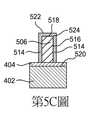
在操作306處,在曝露底層404的表面422之後,間隔物層430接著形成在圖案化的心軸層406上,如第4E圖所示。在一個示例中,間隔物層430是摻雜的含矽層,諸如硼摻雜的矽材料、磷摻雜的矽或其他合適的III族、IV族或V族摻雜的矽材料。在一個示例中,間隔物層430是硼摻雜的矽層。At
在一個實施例中,間隔物層430形成在CVD腔室中,諸如第1圖所描繪的CVD處理腔室100。應注意,間隔物層430可藉由任何合適的沉積處理(諸如PECVD、ALD、SACVD、HDPCVD、旋塗或其他合適的沉積技術)來形成。在一個示例中,間隔物層430具有在約5nm與約25nm之間的厚度。In one embodiment, the
在一個示例中,間隔物層430共形地形成在心軸層406上,共形地襯在心軸層406的頂表面432和側壁434上。咸信由摻雜的矽(諸如硼摻雜的矽材料)製成的間隔物層430可在隨後的圖案化處理期間提供良好的蝕刻選擇性,使得可根據需要在圖案化處理之後獲得間隔物層430的良好輪廓。In one example, the
咸信摻雜的含矽材料(諸如硼摻雜的矽材料)可在比通常用以沉積含矽材料(諸如非摻雜的非晶矽)的溫度低的溫度下沉積。在一些習知實務中,由於由常規CVD處理形成的間隔物層430通常需要利用大於攝氏400度的沉積溫度。相反地,摻雜的矽材料(諸如於此揭露的硼摻雜的矽材料)可藉由具有小於攝氏250度(諸如小於攝氏220度,諸如在約攝氏150度和約攝氏200度之間)的沉積溫度的CVD處理形成,摻雜的矽材料的相對低的沉積在隨後的蝕刻/圖案化處理期間提供了更寬的處理窗口。此外,還可選擇用於附近材料(諸如心軸層406)的材料的更多變化和類型。例如,低的沉積處理溫度允許與間隔物層430接觸的心軸層406由可經受高達攝氏250度的處理溫度而基本上不發生材料交替、膜變形、熱分解(無論是化學上或物理上)和不同類型的變化的材料製成。結果,可選擇某些類型的通常可承受低於攝氏250度的溫度(諸如高於攝氏100度但低於攝氏250度)的碳材料、聚合物材料、有機材料或光阻材料用於心軸層406,這可在操作308處的後續圖案化處理期間增強蝕刻選擇性。此外,間隔物層430的相對低溫的沉積處理也提供最小的微負載效果(micro-loading effect)。It is believed that doped silicon-containing materials (such as boron-doped silicon materials) can be deposited at a lower temperature than the temperatures normally used to deposit silicon-containing materials (such as undoped amorphous silicon). In some conventional practices, the
在操作308處,執行圖案化處理以移除心軸層406,如第4F圖所示,從而自間隔物層430形成間隔物結構431。可在蝕刻腔室(諸如第2圖中所描繪的處理腔室)中執行圖案化處理。藉由供應第一氣體混合物來執行圖案化處理,第一氣體混合物可選擇性地移除具有期望方向性的間隔物層430和心軸層406,使得間隔物層430的某些部分(如,側壁434)可以期望的輪廓保留在基板上,以形成間隔物結構431。在一個示例中,在圖案化處理期間供應的第一氣體混合物可包括用於從間隔物層430各向異性蝕刻含矽材料(特別地,用以各向異性地蝕刻摻雜的含矽材料)的反應性蝕刻劑。At
在一個示例中,第一氣體混合物包括選自由HBr、氯氣(Cl2)、三氟化氮(NF3)、六氟化硫氣體(SF6),含碳和氟的氣體(諸如CF4、CHF3、C4F8及類似者)所組成的群組的含鹵素氣體。在一個特定示例中,第一氣體混合物包括用以蝕刻間隔物層430的HBr和氯氣(Cl2)。第一氣體混合物配置成移除間隔物層430的頂部部分和底部部分而不會顯著地侵蝕間隔物層430的側壁434。在一個示例中,間隔物層430的蝕刻導致間隔物層結構431的基本正方形的頂表面。In an example, the first gas mixture includes selected from HBr, chlorine (Cl2 ), nitrogen trifluoride (NF3 ), sulfur hexafluoride gas (SF6 ), and gas containing carbon and fluorine (such as CF4 , CHF3 , C4 F8 and the like) are halogen-containing gases. In a specific example, the first gas mixture includes HBr and chlorine (Cl2 ) used to etch the
在將第一氣體混合物供應到蝕刻腔室中的同時調節幾個處理參數。在一個實施例中,在存在第一氣體混合物的情況下調節腔室壓力。在一個示例性實施例中,蝕刻腔室中的處理壓力被調節在約2mTorr至約2000mTorr之間,例如,在約100mTorr至約800mTorr之間。可施加RF源和偏壓功率以維持由第一氣體混合物形成的電漿。例如,可將在約100瓦特和約1500瓦特之間(諸如在200瓦特至約800瓦特之間)的RF源功率施加到感應耦合天線源,以將電漿保持在蝕刻腔室內側。在供應第一氣體混合物的同時,施加約小於200瓦特(諸如在約150瓦特和約40瓦特之間)的RF偏壓功率。第一氣體混合物可以在約50sccm至約1000sccm之間的速率流入腔室中。基板溫度維持在約攝氏-20度至約攝氏80度之間。Several processing parameters are adjusted while supplying the first gas mixture into the etching chamber. In one embodiment, the chamber pressure is adjusted in the presence of the first gas mixture. In an exemplary embodiment, the processing pressure in the etching chamber is adjusted between about 2 mTorr and about 2000 mTorr, for example, between about 100 mTorr and about 800 mTorr. An RF source and bias power can be applied to maintain the plasma formed from the first gas mixture. For example, RF source power between about 100 watts and about 1500 watts, such as between 200 watts and about 800 watts, may be applied to the inductively coupled antenna source to keep the plasma inside the etching chamber. While supplying the first gas mixture, an RF bias power of approximately less than 200 watts (such as between approximately 150 watts and approximately 40 watts) is applied. The first gas mixture may flow into the chamber at a rate between about 50 sccm and about 1000 sccm. The temperature of the substrate is maintained at about -20 degrees Celsius to about 80 degrees Celsius.
在供應第一氣體混合物的同時,可改變RF源和偏壓功率範圍,以促進主要移除間隔物層430的某些部分。例如,在供應第一氣體混合物的同時,可根據需要將RF源功率調高(如,從第一RF源功率設定到第二RF源功率設定),而將RF偏壓功率調低(如,從第一RF偏壓功率設定到第二RF偏壓功率設定)。在一個示例中,在已經執行了在約5秒和約20秒之間的時間段的第一RF源和偏壓功率設定之後,第一RF源和偏壓功率設定可被轉換為第二RF源和偏壓功率設定,以繼續圖案化處理。在一個示例中,第二RF源功率設定比第一RF源功率設定高約30%和約80%之間。第二偏壓功率設定比第一偏壓功率設定小約30%和約70%之間。While supplying the first gas mixture, the RF source and bias power range can be changed to facilitate the main removal of certain parts of the
在一個特定示例中,第一RF源功率設定在約500瓦特和約600瓦特之間,且第一RF偏壓功率設定在約50瓦特和約150瓦特之間。第二RF源功率設定在約700瓦特和約900瓦特之間,且第二RF偏壓功率設定在約20瓦特和約100瓦特之間。In a specific example, the first RF source power is set between about 500 watts and about 600 watts, and the first RF bias power is set between about 50 watts and about 150 watts. The second RF source power is set between about 700 watts and about 900 watts, and the second RF bias power is set between about 20 watts and about 100 watts.
在一個示例中,圖案化處理可包括一個或多個處理階段。例如,在供應第一氣體混合物以主要移除頂部部分和底部部分(如,底層404上方的部分)之後,供應第二氣體混合物以主要移除心軸層406。第二氣體混合物包括含氧的氣體混合物及/或載氣,諸如N2、He、Ar及類似者。在一個示例中,根據需要還可利用含碳和氟的氣體,諸如CH2F2,CF4及類似者。在一個特定示例中,第二氣體混合物包括O2和N2或O2、N2和CH2F2。In one example, the patterning process may include one or more processing stages. For example, after supplying the first gas mixture to mainly remove the top portion and the bottom portion (eg, the portion above the bottom layer 404), the second gas mixture is supplied to mainly remove the
在將第二氣體混合物供應到蝕刻腔室中的同時調節幾個處理參數。在一個實施例中,在存在第二氣體混合物的情況下調節腔室壓力。在一個示例性實施例中,蝕刻腔室中的處理壓力被調節在約2mTorr至約2000mTorr之間,例如,在約100mTorr至約800mTorr之間。可施加RF源和偏壓功率以維持由第一氣體混合物形成的電漿。例如,可將在約100瓦特和約1500瓦特之間(諸如在500瓦特和約1500瓦特之間)的RF源功率施加到感應耦合天線源,以將電漿維持在蝕刻腔室內側。在供應第二氣體混合物的同時,施加約小於200瓦特(諸如在約150瓦特和約40瓦特之間)的RF偏壓功率。在供應第二種氣體混合物的同時所施加的RF偏壓功率類似於在供應第一種氣體混合物的同時所施加的第一和第二偏壓功率設定。在一些示例中,在供應第二氣體混合物的同時所施加的RF源功率大於在供應第一氣體混合物的同時所施加的第一和第二源功率設定。第二氣體混合物可以約在50sccm至約1000sccm之間的速率流入腔室中。基板溫度維持在約攝氏-20度至約攝氏80度之間。Several processing parameters are adjusted while supplying the second gas mixture into the etching chamber. In one embodiment, the chamber pressure is adjusted in the presence of the second gas mixture. In an exemplary embodiment, the processing pressure in the etching chamber is adjusted between about 2 mTorr and about 2000 mTorr, for example, between about 100 mTorr and about 800 mTorr. An RF source and bias power can be applied to maintain the plasma formed from the first gas mixture. For example, RF source power between about 100 watts and about 1500 watts (such as between 500 watts and about 1500 watts) may be applied to the inductively coupled antenna source to maintain the plasma inside the etching chamber. While supplying the second gas mixture, an RF bias power of approximately less than 200 watts (such as between approximately 150 watts and approximately 40 watts) is applied. The RF bias power applied while supplying the second gas mixture is similar to the first and second bias power settings applied while supplying the first gas mixture. In some examples, the RF source power applied while supplying the second gas mixture is greater than the first and second source power settings applied while supplying the first gas mixture. The second gas mixture may flow into the chamber at a rate between about 50 sccm and about 1000 sccm. The temperature of the substrate is maintained at about -20 degrees Celsius to about 80 degrees Celsius.
在操作310處,可在間隔物結構431上形成襯墊層440,如第4G圖所示。襯墊層440也可看作是另一間隔物層(如,間隔物在間隔物上的方案),其有助於以所需的減小尺寸來減小在其間界定的開口的尺寸。襯墊層440可為藉由CVD、ALD、旋塗或任何合適的沉積技術而形成的任何合適的含氧化物的材料。在一個示例中,襯墊層440是藉由ALD處理而形成的氧化矽層。應當注意,於此處形成的襯墊層440共形地形成在間隔物結構431上,共形地襯在間隔物結構431的頂表面438和側壁434上。襯墊層440進一步減小了在間隔物結構431之間界定的開口424的尺寸。間隔物結構431可進一步用作遮罩層,以根據需要以減小的小尺寸將特徵轉移到下面的層。At
在操作312處,執行另一圖案化處理以從基板移除襯墊層440的一部分,如第4H圖所示。從基板移除的襯墊層440的部分包括形成在間隔物結構431的頂表面438上和底層404的表面422上的襯墊層440。襯墊層440經歷各向異性蝕刻或圖案化,直到曝露間隔物結構431的頂表面438,從而留下具有側壁部分448襯在間隔物結構431上的襯墊層440。圖案化處理可類似於在操作308處執行的圖案化處理。在一個示例中,操作312導致間隔物結構431的頂表面438基本上為正方形。At
在操作314處,在曝露間隔物結構431的頂表面446之後,執行蝕刻處理以從基板移除間隔物結構431,如第4I圖所示,從而在襯墊層440之間形成具有期望尺寸的開口450。開口450曝露出底層404的頂表面442。襯墊層440隨後可用作遮罩層,遮罩層可促進將特徵轉移到下面的層及/或結構中。如第4I圖所示,形成在基板402上的襯墊層440具有期望的輪廓,該輪廓具有垂直的側壁和最小的基腳、小面或其他不期望的缺陷。藉由利用在間隔物結構431與襯墊層440之間的材料性質差異(如,摻雜的矽材料與氧化矽材料)和心軸層406,可獲得高的蝕刻選擇性,從而在基板上提供襯墊層440的光滑且最小的線條粗糙度作為用於隨後的圖案化處理的硬遮罩。圖案化處理可類似於在操作308處執行的圖案化處理。At
此外,第5A-5G圖描繪了具有不同的膜堆疊結構以形成襯墊層作為遮罩層的類似處理流程,該遮罩層用於在圖案化處理期間將特徵轉移至下面的結構,這也可利用第3圖的方法300的處理順序。類似地,在操作302處,膜堆疊500包括設置在底層404上的心軸層506,如第5A圖所示。在這個示例中,心軸層506可為光阻材料。為心軸層506選擇的光阻材料可為有機材料,其可在高達攝氏200度的熱處理下被維持而基本上不發生熱及/或化學分解。心軸層506的相對較高的熱阻可允許在心軸層506上執行後續的間隔物層沉積而不會分解或損壞,使得允許使用具有高於攝氏150度的處理溫度的CVD處理而在心軸層506上形成間隔物層。In addition, Figures 5A-5G depict a similar process flow with different film stack structures to form a cushion layer as a mask layer, which is used to transfer features to the underlying structure during the patterning process, which also The processing sequence of the
在操作304處,可諸如藉由各向異性蝕刻來修整心軸層506,以將心軸層506的尺寸從第一尺寸508減小到第二減小的尺寸512,如第5B圖所示。At
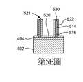
在操作306處,執行間隔物沉積處理以在心軸層506上形成間隔物層524,如第5C圖所示。間隔物層524包括形成在心軸層506的頂表面518上的頂部部分530和形成在心軸層506的側壁上的側壁514。如上所討論的,間隔物層524可與以上所述的藉由CVD處理從摻雜的含矽材料形成的隔物層430相似或相同。At
在操作308處,將心軸層506從基板402移除,並從間隔物層524的側壁514形成間隔物結構521,如第5D圖所示。如上所討論的,由於心軸層506由光阻材料形成,所以利用含氧氣體及/或載氣(諸如N2、He、Ar)來移除的心軸層506。在一個示例中,根據需要,也可利用含碳和氟的氣體(諸如CH2F2、CF4及類似者)。在一個特定示例中,第二氣體混合物包括O2和N2或O2、N2和CH2F2。At
在將含氧氣體及/或載氣供應到蝕刻腔室中的同時,調節幾個處理參數。在一個實施例中,調節在含氧氣體及/或載氣存在下的腔室壓力。在一個示例性實施例中,蝕刻腔室中的處理壓力被調節在約2mTorr至約2000mTorr之間,例如,在約100mTorr和約800mTorr之間。可施加RF源和偏壓功率以維持由第一氣體混合物形成的電漿。例如,可將在約100瓦特和約1500瓦特之間(諸如在500瓦特和約1500瓦特之間)的RF源功率施加到感應耦合天線源,以將電漿維持在蝕刻腔室內側。在供應含氧氣體及/或載氣的同時,施加約小於200瓦特(諸如在約150瓦特和約40瓦特之間)的RF偏壓功率。含氧氣體及/或載氣可以在約50sccm至約1000sccm之間的速率流入腔室中。基板溫度維持在約攝氏-20度至約攝氏80度之間。While supplying oxygen-containing gas and/or carrier gas into the etching chamber, several processing parameters are adjusted. In one embodiment, the chamber pressure in the presence of oxygen-containing gas and/or carrier gas is adjusted. In an exemplary embodiment, the processing pressure in the etching chamber is adjusted between about 2 mTorr and about 2000 mTorr, for example, between about 100 mTorr and about 800 mTorr. An RF source and bias power can be applied to maintain the plasma formed from the first gas mixture. For example, RF source power between about 100 watts and about 1500 watts (such as between 500 watts and about 1500 watts) may be applied to the inductively coupled antenna source to maintain the plasma inside the etching chamber. While supplying oxygen-containing gas and/or carrier gas, an RF bias power of approximately less than 200 watts (such as between approximately 150 watts and approximately 40 watts) is applied. The oxygen-containing gas and/or carrier gas may flow into the chamber at a rate between about 50 sccm and about 1000 sccm. The temperature of the substrate is maintained at about -20 degrees Celsius to about 80 degrees Celsius.
在操作310處,在間隔物結構521上形成襯墊層522,如第5E圖所示。襯墊層522也可視為另一個間隔物層(如,間隔物上間隔的方案),其有助於以所需的減小尺寸來減小如在其間界定的開口的尺寸。襯墊層522共形地形成在間隔物結構521上。類似於上述的襯墊層440,襯墊層552是藉由任何合適的沉積處理(諸如CVD、ALD及類似者)而形成的氧化矽層。At
在操作312處,類似地,襯墊層522被接著圖案化、修整或各向異性地蝕刻,以曝露出間隔物結構521的頂表面530(如,間隔物層516的剩餘側壁514)。圖案化處理可與在操作308處執行的圖案化處理相似。At
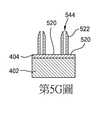
在操作314處,在修整襯墊層522並曝露間隔物結構521的頂表面530之後,可執行圖案化處理以選擇性地移除間隔物結構521,直到曝露底層404的頂表面520,從而在基板402上留下襯墊層522作為遮罩層,用於隨後的圖案化處理。圖案化處理可在襯墊層522和間隔物結構521之間具有高蝕刻選擇性,從而在襯墊層522之間形成具有期望尺寸的開口544。圖案化處理可類似於在操作308處執行的圖案化處理。At
第6A-6F圖描繪了利用如上所述的間隔物層430、516及/或襯墊層440、552藉由多重圖案化處理來形成奈米結構的順序的橫截面圖的另一個示例。間隔物層430、516由摻雜的含矽材料(諸如硼摻雜的矽層)製成。在第6A-6F圖所描繪的示例中,第一對遮罩層604(如,可類似於上述的間隔物層430、516及/或襯墊層440、552)形成在基底層603上,從而於其間界定間距602,如第6A圖所示。間距602可配置成具有在約50nm和約150nm之間(諸如在約60nm和約90nm之間,例如約80nm)的寬度。第一對遮罩層604可界定第一尺寸605。這個步驟可能需要一個微影曝光處理和一個蝕刻/修整處理(諸如各向異性蝕刻),以在基底層603上形成圖案化的第一對遮罩層604。在一個示例中,第一對遮罩層604可根據需要由合適的介電材料製成。在一個示例中,第一對遮罩層604可由摻雜的含矽材料(諸如摻雜硼的矽材料)形成,類似於用以形成上述間隔物層430、516的材料。FIGS. 6A-6F depict another example of a cross-sectional view of the sequence of forming a nanostructure through multiple patterning processes using the spacer layers 430, 516 and/or the liner layers 440, 552 as described above. The spacer layers 430, 516 are made of doped silicon-containing materials (such as boron-doped silicon layers). In the example depicted in FIGS. 6A-6F, a first pair of mask layers 604 (eg, the spacer layers 430, 516 and/or the liner layers 440, 552 described above) are formed on the
隨後,第二對和第三對遮罩層606、608(如,可能類似於上述的間隔物層430、516及/或襯墊層440、552)形成在基底層603上,如第6B圖所示。第二對和第三對遮罩層606、608可各自界定第二尺寸654和第三尺寸652。第二和第三尺寸654、652配置成具有基本相似的寬度。類似地,這種處理可能需要兩個循環的沉積(ALD)處理和蝕刻處理來完成。在一個示例中,第二對和第三對遮罩層606、608可根據需要由合適的介電材料製成。類似地,第二和第三對遮罩層606、608可由摻雜的含矽材料(諸如硼摻雜的矽材料)形成,類似於用以形成上述間隔物層430、516的材料。Subsequently, the second pair and the third pair of mask layers 606, 608 (eg, may be similar to the spacer layers 430, 516 and/or the liner layers 440, 552 described above) are formed on the
另外,可執行第三循環的沉積(ALD)處理和蝕刻處理,以形成第四對遮罩層610(如,可能類似於上述的間隔物層430,516及/或襯墊層440,552),以將間距650進一步減小到較窄的間距660,如第6C圖所示。到目前為止,間距660可縮小到小於約15nm,諸如約10nm。第四對遮罩層610可界定第四尺寸656,類似於由其他遮罩層604、606、608所界定的第一、第二和第三尺寸605、654、652。在一個示例中,第四對遮罩層610可根據需要由合適的介電材料製成。類似地,第四對遮罩層610可由摻雜的含矽材料(諸如摻雜硼的矽材料)形成,類似於上述用以形成間隔物層430、516的材料。In addition, a third cycle of deposition (ALD) processing and etching processing may be performed to form the fourth pair of mask layers 610 (eg, may be similar to the spacer layers 430, 516 and/or the liner layers 440, 552 described above) , To further reduce the
由於間距660和尺寸605、654、652、656均已下降到期望水平,因此可執行蝕刻處理以選擇性地移除遮罩層的一部分,諸如第一對和第三對遮罩層604、608,如第6D圖所示,從而在保留在基底層603上的遮罩層606、610之間產生具有相等的寬度652、605的開口647。需要額外的蝕刻處理以從基底層603選擇性地移除第一對遮罩層604和第三對遮罩層608。(1L)。Since the
在界定了開口647之後,執行最終蝕刻停止以蝕刻基底層606,以在基底層603中形成開口690,如第6E圖所示。隨後,接著移除剩餘的遮罩層606、610,從而留下具有開口664(具有尺寸605、652)的基底層603作為蝕刻遮罩,用於以後的蝕刻處理,如第6F圖所示。After the
應注意每對遮罩層可由不同的材料製成,以便增強其間的蝕刻選擇性。如上所述,可根據需要利用合適的材料(包括非晶矽材料、多晶矽材料、非晶碳材料、有機材料、光阻層、氧化矽材料、摻雜的矽材料(諸如上述在操作306處的硼摻雜的矽材料)及類似者),以根據需要增強蝕刻輪廓。It should be noted that each pair of mask layers can be made of different materials in order to enhance the etching selectivity therebetween. As mentioned above, suitable materials (including amorphous silicon materials, polycrystalline silicon materials, amorphous carbon materials, organic materials, photoresist layers, silicon oxide materials, doped silicon materials (such as the above-mentioned at operation 306) can be used as needed. Boron-doped silicon material) and the like) to enhance the etching profile as needed.
應注意儘管第6A-6F圖中描述的示例是三層間隔物圖案化(SATSP)處理,但是要注意,為間隔物層430、516選擇的材料(諸如摻雜的含矽材料)可用在具有任何數量的間隔物沉積和圖案化處理的任何合適的圖案化處理中。It should be noted that although the example described in Figures 6A-6F is a three-layer spacer patterning (SATSP) process, it should be noted that the materials selected for the spacer layers 430, 516 (such as doped silicon-containing materials) can be used with Any number of spacers are deposited and patterned in any suitable patterning process.
因此,提供了用於多個間隔物圖案化處理以將具有小尺寸的特徵轉移到遮罩層的方法。多個間隔物圖案化處理利用在間隔物層和襯墊層之間的高蝕刻選擇性,使得可獲得襯墊層及/或間隔物層的期望輪廓,其可用作促進奈米尺寸特徵轉移處理的遮罩層。Therefore, a method for a plurality of spacer patterning processes to transfer features with a small size to the mask layer is provided. Multiple spacer patterning processes utilize high etch selectivity between the spacer layer and the spacer layer, so that the desired profile of the spacer layer and/or spacer layer can be obtained, which can be used to promote nano-scale feature transfer The processed mask layer.
儘管前述內容涉及本揭露書的實施例,但是在不背離本揭露書的基本範圍的情況下,可設計本揭露書的其他和進一步的實施例,且本揭露書的範圍由以下的申請專利範圍決定。Although the foregoing content relates to the embodiments of this disclosure, other and further embodiments of this disclosure can be designed without departing from the basic scope of this disclosure, and the scope of this disclosure is defined by the scope of the following patent applications Decided.
100:可流動的化學氣相沉積腔室/沉積腔室/處理腔室101:遠端電漿系統102:第一氣體供應通道104:第二氣體供應通道105:氣體入口組件106:擋板112:蓋114:孔口115:第一電漿區域120:絕緣環125:噴頭133:第二電漿區域135:140:145:150:155:160:165:166:靜電吸盤175:180:190:激發的處理前驅物200:處理腔室202:腔室主體203:基板204:蓋206:內部容積208:側壁210:底部214:內表面218:內襯墊224:226:排氣埠228:泵系統230:噴頭組件232:入口埠232’:入口埠232”:入口埠234:內部區域236:外部區域238:通道240:光學監視系統241:匹配網路242:窗口243:RF源功率248:基板支撐基座組件250:控制器252:中央處理單元(CPU)254:記憶體256:支持電路258:氣體面板262:安裝板264:基底266:靜電吸盤268:導管270:導管272:流體源274:嵌入式隔離器276:加熱器277:遠端電漿源278:功率源280:電極282:夾持功率源284:RF偏壓功率源286:RF偏壓功率源288:匹配電路289:偏壓功率源290:溫度感測器292:溫度感測器300:方法302:操作304:操作306:操作308:操作310:操作312:操作314:操作400:膜堆疊402:基板404:底層406:心軸層408:硬遮罩層410:光阻層412:開口414:光阻層416:部分418:開口420:422:表面424:開口430:間隔物層431:間隔物結構432:頂表面434:側壁438:頂表面440:襯墊層442:頂表面446:頂表面448:側壁部分450:開口500:膜堆疊506:心軸層508:第一尺寸512:第二減小的尺寸514:側壁516:間隔物層518:頂表面520:頂表面521:間隔物結構522:襯墊層524:間隔物層530:頂部部分/頂表面544:開口552:襯墊層602:間距603:基底層604:遮罩層605:第一尺寸/寬度/尺寸606:遮罩層/基底層608:遮罩層610:遮罩層647:開口650:間距652:第三尺寸/寬度/尺寸654:第二尺寸/尺寸656:第四尺寸/尺寸660:間距664:開口690:開口100: Flowable chemical vapor deposition chamber/deposition chamber/processing chamber101: Remote Plasma System102: The first gas supply channel104: Second gas supply channel105: Gas inlet assembly106: bezel112: cover114: Orifice115: The first plasma region120: Insulation ring125: print head133: Second Plasma Region135:140:145:150:155:160:165:166: Electrostatic chuck175:180:190: Excited Processing Precursors200: processing chamber202: Chamber body203: Substrate204: cover206: Internal volume208: Sidewall210: bottom214: inner surface218: inner liner224:226: Exhaust Port228: Pump System230: print head assembly232: Ingress port232’: entrance port232": entrance port234: Internal area236: Outer Area238: Channel240: Optical Surveillance System241: matching network242: Window243: RF source power248: Substrate support base assembly250: Controller252: Central Processing Unit (CPU)254: Memory256: Support circuit258: Gas Panel262: mounting plate264: Base266: Electrostatic chuck268: Catheter270: Catheter272: Fluid Source274: Embedded Isolator276: heater277: Remote Plasma Source278: Power Source280: Electrode282: Clamping power source284: RF bias power source286: RF bias power source288: matching circuit289: Bias power source290: temperature sensor292: Temperature Sensor300: method302: Operation304: Operation306: Operation308: Operation310: Operation312: Operation314: Operation400: Membrane stack402: Substrate404: bottom layer406: Mandrel Layer408: hard mask layer410: photoresist layer412: open414: photoresist layer416: part418: open420:422: Surface424: open430: spacer layer431: Spacer structure432: top surface434: Sidewall438: Top Surface440: Cushion layer442: top surface446: top surface448: side wall part450: opening500: Membrane stack506: Mandrel Layer508: first size512: The second reduced size514: Sidewall516: spacer layer518: top surface520: top surface521: Spacer structure522: Cushion layer524: Spacer layer530: top part/top surface544: open552: Cushion layer602: Spacing603: basal layer604: Mask layer605: The first size/width/size606: mask layer/base layer608: Mask layer610: Mask layer647: open650: pitch652: third size/width/size654: second size/size656: The fourth size / size660: pitch664: open690: open
為了可詳細地理解本揭露書的實施例的上述特徵的方式,可藉由參考實施例來獲得簡要概述於上的本揭露書的更詳細的描述,一些實施例顯示在附隨的圖式中。然而,應當注意,附隨的圖式僅顯示了本揭露書的典型實施例,且因此不應被認為是對其範圍的限制,因為本揭露書可允許其他等效的實施例。In order to understand the above-mentioned features of the embodiments of the present disclosure in detail, a more detailed description of the present disclosure briefly summarized above can be obtained by referring to the embodiments. Some embodiments are shown in the accompanying drawings. . However, it should be noted that the accompanying drawings only show typical embodiments of the present disclosure, and therefore should not be considered as limiting its scope, because the present disclosure may allow other equivalent embodiments.
第1圖描繪了根據本揭露書的一個實施例的可用以執行沉積製程的處理腔室;Figure 1 depicts a processing chamber that can be used to perform a deposition process according to an embodiment of the present disclosure;
第2圖描繪了根據本揭露書的一個實施例的可用以執行蝕刻製程的處理腔室;Figure 2 depicts a processing chamber that can be used to perform an etching process according to an embodiment of the present disclosure;
第3圖描繪了根據本揭露書的一個實施例的用於執行圖案化處理以形成奈米結構的方法的流程圖;Figure 3 depicts a flowchart of a method for performing patterning processing to form a nanostructure according to an embodiment of the present disclosure;
第4A-4I圖描繪了根據本揭露書的一個實施例的藉由第3圖的方法形成奈米結構的序列的橫截面的一個示例;Figures 4A-4I depict an example of a cross-section of a sequence of forming a nanostructure by the method of Figure 3 according to an embodiment of the present disclosure;
第5A-5G圖描繪了根據本揭露書的一個實施例的藉由第3圖的方法形成奈米結構的序列的橫截面的一個示例;及Figures 5A-5G depict an example of a cross-section of a sequence of nanostructures formed by the method of Figure 3 according to an embodiment of the present disclosure; and
第6A-6F圖描繪了根據本揭露書的一個實施例的藉由利用在第3圖的方法中所利用的間隔物層來形成奈米結構的序列的橫截面的另一示例。FIGS. 6A-6F depict another example of a cross section of a sequence of forming a nanostructure by using the spacer layer used in the method of FIG. 3 according to an embodiment of the present disclosure.
為促進理解,在可能的情況下使用了相同的元件符號來表示圖式中共有的相同元件。可預期,在一個實施例中揭露的元件可在沒有具體敘述的情況下有益地用於其他實施例。To facilitate understanding, the same element symbols are used where possible to represent the same elements in the drawings. It is expected that the elements disclosed in one embodiment can be beneficially used in other embodiments without specific description.
國內寄存資訊(請依寄存機構、日期、號碼順序註記)無國外寄存資訊(請依寄存國家、機構、日期、號碼順序註記)無Domestic deposit information (please note in the order of deposit institution, date and number)noForeign hosting information (please note in the order of hosting country, institution, date and number)no
300:方法300: method
302:操作302: Operation
304:操作304: Operation
306:操作306: Operation
308:操作308: Operation
310:操作310: Operation
312:操作312: Operation
314:操作314: Operation
Claims (20)
Translated fromChineseApplications Claiming Priority (2)
| Application Number | Priority Date | Filing Date | Title |
|---|---|---|---|
| US201962835290P | 2019-04-17 | 2019-04-17 | |
| US62/835,290 | 2019-04-17 |
Publications (1)
| Publication Number | Publication Date |
|---|---|
| TW202105472Atrue TW202105472A (en) | 2021-02-01 |
Family
ID=72830841
Family Applications (1)
| Application Number | Title | Priority Date | Filing Date |
|---|---|---|---|
| TW109111898ATW202105472A (en) | 2019-04-17 | 2020-04-09 | Multiple spacer patterning schemes |
Country Status (6)
| Country | Link |
|---|---|
| US (3) | US11315787B2 (en) |
| JP (1) | JP7357688B2 (en) |
| KR (1) | KR20210129271A (en) |
| CN (1) | CN113614880A (en) |
| TW (1) | TW202105472A (en) |
| WO (1) | WO2020214326A1 (en) |
Cited By (1)
| Publication number | Priority date | Publication date | Assignee | Title |
|---|---|---|---|---|
| TWI819796B (en)* | 2021-12-07 | 2023-10-21 | 台灣積體電路製造股份有限公司 | Method of forming semiconductor structure |
Families Citing this family (6)
| Publication number | Priority date | Publication date | Assignee | Title |
|---|---|---|---|---|
| US11881402B2 (en) | 2020-09-30 | 2024-01-23 | Applied Materials, Inc. | Self aligned multiple patterning |
| US20220189771A1 (en)* | 2020-12-10 | 2022-06-16 | Applied Materials, Inc. | Underlayer film for semiconductor device formation |
| US12272564B2 (en) | 2020-12-15 | 2025-04-08 | Applied Materials, Inc. | Tin oxide and tin carbide materials for semiconductor patterning applications |
| US12374583B2 (en)* | 2021-05-12 | 2025-07-29 | Taiwan Semiconductor Manufacturing Co., Ltd. | Semiconductor devices and methods of manufacture |
| KR20230014339A (en)* | 2021-07-21 | 2023-01-30 | 세메스 주식회사 | Method and apparatus for treating substrate |
| US11830744B1 (en)* | 2022-05-31 | 2023-11-28 | Nanya Technology Corporation | Method of preparing active areas |
Family Cites Families (31)
| Publication number | Priority date | Publication date | Assignee | Title |
|---|---|---|---|---|
| JP4401033B2 (en)* | 2001-03-19 | 2010-01-20 | Azエレクトロニックマテリアルズ株式会社 | Negative photosensitive resin composition and display device using the same |
| US6784110B2 (en)* | 2002-10-01 | 2004-08-31 | Jianping Wen | Method of etching shaped features on a substrate |
| US7294581B2 (en) | 2005-10-17 | 2007-11-13 | Applied Materials, Inc. | Method for fabricating silicon nitride spacer structures |
| KR100764375B1 (en)* | 2005-12-15 | 2007-10-08 | 주식회사 하이닉스반도체 | Polymer for hard mask of semiconductor device and composition containing same |
| US7611980B2 (en)* | 2006-08-30 | 2009-11-03 | Micron Technology, Inc. | Single spacer process for multiplying pitch by a factor greater than two and related intermediate IC structures |
| US7811924B2 (en) | 2008-06-16 | 2010-10-12 | Applied Materials, Inc. | Air gap formation and integration using a patterning cap |
| US9892917B2 (en) | 2010-04-15 | 2018-02-13 | Lam Research Corporation | Plasma assisted atomic layer deposition of multi-layer films for patterning applications |
| US8735291B2 (en)* | 2011-08-25 | 2014-05-27 | Tokyo Electron Limited | Method for etching high-k dielectric using pulsed bias power |
| US20130189845A1 (en) | 2012-01-19 | 2013-07-25 | Applied Materials, Inc. | Conformal amorphous carbon for spacer and spacer protection applications |
| WO2014124795A1 (en)* | 2013-02-14 | 2014-08-21 | Asml Netherlands B.V. | Methods for providing spaced lithography features on a substrate by self-assembly of block copolymers |
| US9257293B2 (en) | 2013-03-14 | 2016-02-09 | Applied Materials, Inc. | Methods of forming silicon nitride spacers |
| US8932947B1 (en)* | 2013-07-23 | 2015-01-13 | Applied Materials, Inc. | Methods for forming a round bottom silicon trench recess for semiconductor applications |
| US9466486B2 (en)* | 2013-08-30 | 2016-10-11 | Taiwan Semiconductor Manufacturing Company, Ltd. | Method for integrated circuit patterning |
| US20150064921A1 (en)* | 2013-08-30 | 2015-03-05 | Applied Materials, Inc. | Low temperature plasma anneal process for sublimative etch processes |
| US9698015B2 (en) | 2013-10-21 | 2017-07-04 | Applied Materials, Inc. | Method for patterning a semiconductor substrate |
| US9123776B2 (en) | 2013-12-04 | 2015-09-01 | Taiwan Semiconductor Manufacturing Company, Ltd. | Self-aligned double spacer patterning process |
| CN106537576B (en)* | 2014-04-01 | 2019-08-27 | 应用材料公司 | Integrated Metal Spacer and Air Gap Interconnects |
| US9269590B2 (en) | 2014-04-07 | 2016-02-23 | Applied Materials, Inc. | Spacer formation |
| US9548201B2 (en) | 2014-06-20 | 2017-01-17 | Applied Materials, Inc. | Self-aligned multiple spacer patterning schemes for advanced nanometer technology |
| US9941139B2 (en)* | 2014-09-10 | 2018-04-10 | Taiwan Semiconductor Manufacturing Company, Ltd. | Method of semiconductor integrated circuit fabrication |
| US9472414B2 (en)* | 2015-02-13 | 2016-10-18 | Taiwan Semiconductor Manufacturing Company, Ltd. | Self-aligned multiple spacer patterning process |
| US9741566B2 (en)* | 2015-03-30 | 2017-08-22 | Applied Materials, Inc. | Methods for manufacturing a spacer with desired profile in an advanced patterning process |
| CN106298519A (en)* | 2015-05-15 | 2017-01-04 | 联华电子股份有限公司 | Method for forming semiconductor structure |
| US10020196B2 (en)* | 2015-09-24 | 2018-07-10 | Tokyo Electron Limited | Methods of forming etch masks for sub-resolution substrate patterning |
| US20190002736A1 (en)* | 2015-12-18 | 2019-01-03 | 3M Innovative Properties Company | Adhesive article liner with sorbent material |
| US10629435B2 (en)* | 2016-07-29 | 2020-04-21 | Lam Research Corporation | Doped ALD films for semiconductor patterning applications |
| WO2018052760A1 (en)* | 2016-09-13 | 2018-03-22 | Applied Materials, Inc. | Borane mediated dehydrogenation process from silane and alkylsilane species for spacer and hardmask application |
| US20180323061A1 (en) | 2017-05-03 | 2018-11-08 | Tokyo Electron Limited | Self-Aligned Triple Patterning Process Utilizing Organic Spacers |
| US10510540B2 (en) | 2017-07-15 | 2019-12-17 | Micromaterials Llc | Mask scheme for cut pattern flow with enlarged EPE window |
| WO2019022826A1 (en)* | 2017-07-24 | 2019-01-31 | Applied Materials, Inc. | Pre-treatment approach to improve continuity of ultra-thin amorphous silicon film on silicon oxide |
| CN112189255B (en)* | 2018-03-20 | 2024-05-28 | 东京毅力科创株式会社 | Self-aligned multiple patterning method and semiconductor processing method |
- 2020
- 2020-03-17USUS16/821,759patent/US11315787B2/enactiveActive
- 2020-03-19KRKR1020217033789Apatent/KR20210129271A/ennot_activeCeased
- 2020-03-19CNCN202080021414.6Apatent/CN113614880A/enactivePending
- 2020-03-19JPJP2021560250Apatent/JP7357688B2/enactiveActive
- 2020-03-19WOPCT/US2020/023681patent/WO2020214326A1/ennot_activeCeased
- 2020-04-09TWTW109111898Apatent/TW202105472A/enunknown
- 2020-05-05USUS16/867,095patent/US11527408B2/enactiveActive
- 2022
- 2022-11-30USUS18/072,457patent/US20230093450A1/enactivePending
Cited By (1)
| Publication number | Priority date | Publication date | Assignee | Title |
|---|---|---|---|---|
| TWI819796B (en)* | 2021-12-07 | 2023-10-21 | 台灣積體電路製造股份有限公司 | Method of forming semiconductor structure |
Also Published As
| Publication number | Publication date |
|---|---|
| US20230093450A1 (en) | 2023-03-23 |
| WO2020214326A1 (en) | 2020-10-22 |
| US11315787B2 (en) | 2022-04-26 |
| CN113614880A (en) | 2021-11-05 |
| JP7357688B2 (en) | 2023-10-06 |
| US20200335338A1 (en) | 2020-10-22 |
| US20200335339A1 (en) | 2020-10-22 |
| KR20210129271A (en) | 2021-10-27 |
| US11527408B2 (en) | 2022-12-13 |
| JP2022529610A (en) | 2022-06-23 |
Similar Documents
| Publication | Publication Date | Title |
|---|---|---|
| US11527408B2 (en) | Multiple spacer patterning schemes | |
| US10438807B2 (en) | Low roughness EUV lithography | |
| CN101312126B (en) | Method of forming amorphous carbon film and method of manufacturing semiconductor device using same | |
| TW201937575A (en) | Method of spacer-defined direct patterning in semiconductor fabrication | |
| US9214377B2 (en) | Methods for silicon recess structures in a substrate by utilizing a doping layer | |
| US11881402B2 (en) | Self aligned multiple patterning | |
| TW202105471A (en) | A film stack for lithography applications | |
| US20220189771A1 (en) | Underlayer film for semiconductor device formation | |
| CN101431015B (en) | Method of reducing photoresist mask collapse and method of patterning anti-reflective coating | |
| US20150118832A1 (en) | Methods for patterning a hardmask layer for an ion implantation process | |
| CN110729187A (en) | Plasma etching method and plasma etching apparatus | |
| CN103843110A (en) | Double patterning etching process | |
| US20040262263A1 (en) | Etching methods and apparatus and substrate assemblies produced therewith | |
| JP2005045053A (en) | Method for manufacturing semiconductor device | |
| TWI817066B (en) | Methods for etching a material layer for semiconductor applications | |
| TW202308466A (en) | Plasma processing method, plasma processing apparatus, and plasma processing system | |
| WO2020215183A1 (en) | Methods for etching a material layer for semiconductor applications | |
| JP7746601B2 (en) | Dry development method and dry development apparatus | |
| US11456173B2 (en) | Methods for modifying photoresist profiles and tuning critical dimensions | |
| US20250258433A1 (en) | Underlayer treatment for improved photoresist adhesion | |
| O'Connell | An Etching Study for Self-Aligned Double Patterning | |
| WO2023239689A1 (en) | Ruthenium carbide for dram capacitor mold patterning | |
| CN120614860A (en) | Gate structure forming method |