TW202103012A - Multi-die system - Google Patents
Multi-die systemDownload PDFInfo
- Publication number
- TW202103012A TW202103012ATW108132106ATW108132106ATW202103012ATW 202103012 ATW202103012 ATW 202103012ATW 108132106 ATW108132106 ATW 108132106ATW 108132106 ATW108132106 ATW 108132106ATW 202103012 ATW202103012 ATW 202103012A
- Authority
- TW
- Taiwan
- Prior art keywords
- chip
- access
- signal
- volatile memory
- control signal
- Prior art date
Links
Images


Classifications
- G—PHYSICS
- G06—COMPUTING OR CALCULATING; COUNTING
- G06F—ELECTRIC DIGITAL DATA PROCESSING
- G06F3/00—Input arrangements for transferring data to be processed into a form capable of being handled by the computer; Output arrangements for transferring data from processing unit to output unit, e.g. interface arrangements
- G06F3/06—Digital input from, or digital output to, record carriers, e.g. RAID, emulated record carriers or networked record carriers
- G06F3/0601—Interfaces specially adapted for storage systems
- G06F3/0628—Interfaces specially adapted for storage systems making use of a particular technique
- G06F3/0655—Vertical data movement, i.e. input-output transfer; data movement between one or more hosts and one or more storage devices
- G06F3/0659—Command handling arrangements, e.g. command buffers, queues, command scheduling
- G—PHYSICS
- G06—COMPUTING OR CALCULATING; COUNTING
- G06F—ELECTRIC DIGITAL DATA PROCESSING
- G06F13/00—Interconnection of, or transfer of information or other signals between, memories, input/output devices or central processing units
- G06F13/14—Handling requests for interconnection or transfer
- G06F13/16—Handling requests for interconnection or transfer for access to memory bus
- G06F13/1605—Handling requests for interconnection or transfer for access to memory bus based on arbitration
- G—PHYSICS
- G06—COMPUTING OR CALCULATING; COUNTING
- G06F—ELECTRIC DIGITAL DATA PROCESSING
- G06F13/00—Interconnection of, or transfer of information or other signals between, memories, input/output devices or central processing units
- G06F13/14—Handling requests for interconnection or transfer
- G06F13/16—Handling requests for interconnection or transfer for access to memory bus
- G06F13/1668—Details of memory controller
- G—PHYSICS
- G06—COMPUTING OR CALCULATING; COUNTING
- G06F—ELECTRIC DIGITAL DATA PROCESSING
- G06F3/00—Input arrangements for transferring data to be processed into a form capable of being handled by the computer; Output arrangements for transferring data from processing unit to output unit, e.g. interface arrangements
- G06F3/06—Digital input from, or digital output to, record carriers, e.g. RAID, emulated record carriers or networked record carriers
- G06F3/0601—Interfaces specially adapted for storage systems
- G06F3/0602—Interfaces specially adapted for storage systems specifically adapted to achieve a particular effect
- G06F3/061—Improving I/O performance
- G06F3/0613—Improving I/O performance in relation to throughput
- G—PHYSICS
- G06—COMPUTING OR CALCULATING; COUNTING
- G06F—ELECTRIC DIGITAL DATA PROCESSING
- G06F3/00—Input arrangements for transferring data to be processed into a form capable of being handled by the computer; Output arrangements for transferring data from processing unit to output unit, e.g. interface arrangements
- G06F3/06—Digital input from, or digital output to, record carriers, e.g. RAID, emulated record carriers or networked record carriers
- G06F3/0601—Interfaces specially adapted for storage systems
- G06F3/0602—Interfaces specially adapted for storage systems specifically adapted to achieve a particular effect
- G06F3/0626—Reducing size or complexity of storage systems
- G—PHYSICS
- G06—COMPUTING OR CALCULATING; COUNTING
- G06F—ELECTRIC DIGITAL DATA PROCESSING
- G06F3/00—Input arrangements for transferring data to be processed into a form capable of being handled by the computer; Output arrangements for transferring data from processing unit to output unit, e.g. interface arrangements
- G06F3/06—Digital input from, or digital output to, record carriers, e.g. RAID, emulated record carriers or networked record carriers
- G06F3/0601—Interfaces specially adapted for storage systems
- G06F3/0668—Interfaces specially adapted for storage systems adopting a particular infrastructure
- G06F3/0671—In-line storage system
- G06F3/0683—Plurality of storage devices
- G06F3/0688—Non-volatile semiconductor memory arrays
Landscapes
- Engineering & Computer Science (AREA)
- Theoretical Computer Science (AREA)
- Physics & Mathematics (AREA)
- General Engineering & Computer Science (AREA)
- General Physics & Mathematics (AREA)
- Human Computer Interaction (AREA)
- Bus Control (AREA)
Abstract
Description
Translated fromChinese本發明涉及一種多晶片系統,尤指一種能共用非揮發性記憶體的多晶片系統。The invention relates to a multi-chip system, in particular to a multi-chip system capable of sharing non-volatile memory.
多晶片系統可提高系統效能並且滿足單晶片無法支援的系統結構。傳統上,具有獨立處理功能的晶片)具有專用的非揮發性記憶體(例如Flash Memory),可用於指令,資料存儲和晶片內執行(execute-in-place),而且每個晶片都可獨立運作,每個晶片皆有電源電路以及時脈電路以供自己晶片所使用。因此,每個晶片的功能、應用、操作電壓和時脈頻率是完全獨立的,所以每個獨立晶片的功能、應用、操作電壓及/或頻率不相同,導致每個晶片內的訊號的位準及/或頻率不同。此外,由於每個晶片為獨立運作,因此各個晶片內的操作時脈訊號彼此不同步。也就是說,即使各個晶片內的操作時脈訊號的頻率相同,各個晶片內的操作時脈訊號也不會同步。由於上述眾多原因而導致至少二晶片要整合成可共用一個非揮發性記憶體的難度是高的,也因上述原因阻卻了晶片工程師將至少二晶片要整合成可共用一個非揮發性記憶體的動機,因此,現有的多晶片系統皆需要多個專用非揮發性記憶體。然而,在各晶片中使用專用非揮發性記憶體系統會產生較高的成本,並且每個非揮發性記憶體的頻寬利用率無法最大化。因此需要新的解決方案。Multi-chip systems can improve system performance and meet system structures that cannot be supported by a single chip. Traditionally, chips with independent processing functions have dedicated non-volatile memory (such as Flash Memory), which can be used for instructions, data storage and execute-in-place, and each chip can operate independently , Each chip has a power supply circuit and a clock circuit for its own chip. Therefore, the function, application, operating voltage and clock frequency of each chip are completely independent, so the function, application, operating voltage and/or frequency of each independent chip are not the same, resulting in the level of the signal in each chip And/or the frequency is different. In addition, since each chip operates independently, the operating clock signals in each chip are not synchronized with each other. In other words, even if the frequency of the operating clock signal in each chip is the same, the operating clock signal in each chip will not be synchronized. Due to the many reasons mentioned above, it is difficult for at least two chips to be integrated to share a non-volatile memory, and the above reasons prevent chip engineers from integrating at least two chips to share a non-volatile memory. Therefore, existing multi-chip systems require multiple dedicated non-volatile memories. However, using a dedicated non-volatile memory system in each chip will incur higher costs, and the bandwidth utilization of each non-volatile memory cannot be maximized. Therefore, a new solution is needed.
本發明實施例提供一種多晶片系統,包括:一非揮發性記憶體;一第一晶片,具有一第一操作時脈,該第一晶片包括:一第一處理器,用以產生一第一控制訊號;一第一存取控制器,用以根據該第一控制訊號產生一第一存取訊號以存取該非揮發性記憶體;一第一匯流排控制電路,耦接於該第一處理器和該第一存取控制器之間,用以控制該第一控制訊號的傳送;及一第一輸入/輸出控制電路,耦接於該第一存取控制器和該非揮發性記憶體之間,用以控制該第一存取訊號的傳送;一第二晶片,具有一第二操作時脈,該第二晶片包括:一第二處理器,用以產生一第二控制訊號;一第二存取控制器,用以根據該第二控制訊號產生一第二存取訊號以存取該非揮發性記憶體;一第二匯流排控制電路,耦接於該第二處理器和該第二存取控制器之間,用以控制該第二控制訊號的傳送;及一第二輸入/輸出控制電路,耦接於該第二存取控制器和該非揮發性記憶體之間,用以控制該第二存取訊號的傳送;及一仲裁器,設置於該多晶片系統內, 用以根據該第一控制訊號和該第二控制訊號產生一仲裁訊號;其中,該第一匯流排控制電路、該第二匯流排控制電路、該第一輸入/輸出控制電路和該第二輸入/輸出控制電路係根據該仲裁訊號來控制;其中該第一操作時脈和該第二操作時脈不同步。An embodiment of the present invention provides a multi-chip system, including: a non-volatile memory; a first chip having a first operating clock, the first chip including: a first processor for generating a first Control signal; a first access controller for generating a first access signal to access the non-volatile memory according to the first control signal; a first bus control circuit coupled to the first processing Between the first access controller and the first access controller to control the transmission of the first control signal; and a first input/output control circuit coupled to the first access controller and the non-volatile memory Between, for controlling the transmission of the first access signal; a second chip with a second operating clock, the second chip including: a second processor for generating a second control signal; Two access controllers for generating a second access signal to access the non-volatile memory according to the second control signal; a second bus control circuit coupled to the second processor and the second Between the access controllers for controlling the transmission of the second control signal; and a second input/output control circuit, coupled between the second access controller and the non-volatile memory, for controlling Transmission of the second access signal; and an arbiter, which is arranged in the multi-chip system, for generating an arbitration signal according to the first control signal and the second control signal; wherein, the first bus control circuit , The second bus control circuit, the first input/output control circuit and the second input/output control circuit are controlled according to the arbitration signal; wherein the first operating clock and the second operating clock are not synchronized .
本發明實施例提供一種操作多晶片系統的方法,該系統包括一第一晶片,一第二晶片和一仲裁器,該第一晶片包括第一處理器與一第一存取控制器,該第二晶片包括第二處理器與一第二存取控制器,該方法包括:該第一處理器產生一第一控制訊號,以通過一第一路徑向傳送至該第一存取控制器產生一第一控制訊號;該第一存取控制器根據該第一控制訊號產生一第一存取訊號,以通過一第二路徑存取一非揮發性記憶體;該第二處理器產生一第二控制訊號,以通過一第三路徑傳送至向該第二存取控制器產生一第二控制訊號;該第二晶片中的該第二存取控制器根據該第二控制訊號產生一第二存取訊號,以通過一第四路徑存取該非揮發性記憶體;該仲裁器根據該第一控制訊號和該第二控制訊號產生一仲裁訊號;及根據該仲裁訊號控制該第一路徑,該第二路徑,該第三路徑及該第四路徑;其中,具有一第一操作電壓和一第一操作時脈的該第一晶片及具有一第二操作電壓和一第二操作時脈的該第二晶片係為獨立運作。An embodiment of the present invention provides a method for operating a multi-chip system. The system includes a first chip, a second chip, and an arbiter. The first chip includes a first processor and a first access controller. The two chips include a second processor and a second access controller. The method includes: the first processor generates a first control signal to transmit to the first access controller through a first path to generate a A first control signal; the first access controller generates a first access signal according to the first control signal to access a non-volatile memory through a second path; the second processor generates a second The control signal is transmitted through a third path to generate a second control signal to the second access controller; the second access controller in the second chip generates a second memory according to the second control signal To obtain a signal to access the non-volatile memory through a fourth path; the arbiter generates an arbitration signal according to the first control signal and the second control signal; and controls the first path according to the arbitration signal, the second Two paths, the third path and the fourth path; wherein, the first chip having a first operating voltage and a first operating clock, and the first chip having a second operating voltage and a second operating clock The two chips are operated independently.
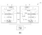
圖1是本發明實施例的多晶片系統100的示意圖。多晶片系統100包括非揮發性記憶體10,第一晶片20及第二晶片30。第一晶片20包括第一處理器26,第一匯流排21,仲裁器22,第一匯流排控制電路23、第一存取控制器24,以及第一輸入/輸出控制電路25。其中,該第一晶片與該第二晶片係可獨立操作,換言之,該第一晶片與該第二晶片電氣特性中的至少一部份特性是實質上不完全相同或完全不同。其中,仲裁器22用於仲裁多晶片(20,30)存取非揮發性記憶體10。第一匯流排控制電路23耦接於第一處理器26和第一存取控制器24之間,並受仲裁器22的控制。第一匯流排控制電路23係控制(如:延遲(delay)、暫存)來自第一處理器26的存取控制訊號。第一存取控制器24控制電路用以根據第一處理器26的存取控制訊號以存取非揮發性記憶體10。第一輸入/輸出控制電路25耦接耦接於第一存取控制器24和非揮發性記憶體10之間,並受仲裁器22的控制。第一輸入/輸出控制電路25係控制(如:延遲、暫存) 來自第一存取控制器24的存取訊號。第二晶片30包括第二處理器36,第二匯流排31,第二匯流排控制電路33,第二存取控制器34,第二輸入/輸出控制電路35。其中,第二匯流排控制電路33耦接於第二處理器36和第二存取控制器34之間,並接受仲裁器22的控制。第二匯流排控制電路33用於控制(如:延遲(delay)、暫存)來自第二處理器36的存取控制訊號,第二存取控制器34控制電路根據第二處理器36的存取控制訊號存取非揮發性記憶體10,以及第二輸入/輸出控制電路35耦接於第二存取控制器34與非揮發性記憶體10之間,用於控制(如:延遲(delay) 、暫存) 來自第二存取控制器34的存取訊號。多晶片系統100中的各元件的電性連接關係可同時參閱本說明書的圖1。在一實施例中,仲裁器22係設置於第一晶片20及第二晶片30之外。在一實施例中,第一晶片20及第二晶片30的電源設定(如正常模式、睡眠模式、待機模式及關機模式)彼此不同,可彼此獨自運作。在一實施例中,若第一晶片20及第二晶片30的效能不同,則仲裁器22可設置於效能較高的晶片,舉例而言,第一晶片20具有比第二晶片30較快的時脈,較高的頻寬,較高階的結構等。舉例而言,正常模式下,第一晶片20具有比第二晶片30較快的時脈,較高的頻寬,較強的運算能力等。FIG. 1 is a schematic diagram of a
在一實施例中,第一晶片20與第二晶片30各具有存取非揮發性記憶體10的優先權。在一實施例中,優先權相同時,仲裁器22可用循環調度的方式決定晶片存取非揮發性記憶體10的順序。在一實施例中,優先權等級與晶片的功能(應用)相關。在一實施例中,優先權等級與晶片效能相關。在一實施例中,第一晶片20具有比第二晶片30更高存取非揮發性記憶體10的優先權。第一晶片20與第二晶片30具有不同時脈,頻寬,結構及/或配置。因此,第一匯流排21與第二匯流排31具有不同時脈,頻寬,結構及/或配置,第一晶片20可具有比第二晶片30更快的系統時脈。第一匯流排21與第二匯流排31可為AHB, AXI 或其他類型的匯流排。非揮發性記憶體10可具有QSPI或其他類型的介面。另外,若發出超過一個請求,仲裁器22可授權給具有最高優先權的請求。In one embodiment, the
當第一晶片20或/及第二晶片30需要存取非揮發性記憶體10時,第一匯流排控制電路23或/及第二匯流排控制電路33產生請求訊號ReqA及ReqB至仲裁器22。當仲裁器22發出授權訊號GntA至第一匯流排控制電路23時,第一匯流排控制電路23會傳遞存取控制訊號至第一存取控制器24。當仲裁器22發出授權訊號GntB至第二匯流排控制電路33時,第二匯流排控制電路33會傳遞存取控制訊號至第二存取控制器34。相反地,當仲裁器22停止發出授權訊號GntA至第一匯流排控制電路23,以停止或延遲傳遞存取控制訊號並且傳送訊息至第一晶片20和第一存取控制器24,當仲裁器22停止發出授權訊號GntB至第二匯流排控制電路33會停止或延遲傳遞存取制控訊號並且傳送訊息至第二晶片30和第二存取控制器34。When the
當仲裁器22發出授權訊號GntA至第一輸入/輸出控制電路25時,第一輸入/輸出控制電路25會傳遞存取訊號至非揮發性記憶體10。當仲裁器22發出授權訊號GntB至第二輸入/輸出控制電路35時,第二匯流排控制電路35會傳遞存取訊號至非揮發性記憶體10。相反地,當仲裁器22停止發出授權訊號GntA時,第一輸入/輸出控制電路25會停止或延遲傳遞存取訊號至非揮發性記憶體10,而當仲裁器22停止發出授權訊號GntB時,第二輸入/輸出控制電路35會停止或延遲傳遞存取訊號至非揮發性記憶體10。When the
圖2是仲裁器22仲裁過程操作訊號的示意圖。圖2示出了仲裁器22的時脈訊號ClkA,仲裁器22產生的授權訊號GntA、GntB,在第一晶片20的請求訊號ReqA,在第二晶片30的請求訊號ReqB。其中,由於仲裁器22係不位於第二晶片30中,故該請求訊號ReqB與該授權訊號GntB係為不同步,且/或其位準及/或頻率不同。FIG. 2 is a schematic diagram of the operation signals of the
在起始階段,仲裁器22通過傳送授權訊號GntA至第一匯流排控制電路23及第一輸入/輸出控制電路25預設授權第一晶片20存取非揮發性記憶體10,此時,第一晶片20即可存取非揮發性記憶體10。在第一晶片20執行存取後,第一晶片20會停止發送請求訊號ReqA一週期以使仲裁器22可執行仲裁。若第一晶片20在該周期繼續發送請求訊號ReqA,則仲裁器22可通過發送授權訊號GntA持續授權第一晶片20存取非揮發性記憶體10。在某些實施例中,當第一晶片20已經完成一定數量的存取並且第二晶片30已將請求訊號ReqB發送至仲裁器22時,無論第一晶片20是否有待處理請求,仲裁器22都會通過發送授權訊號GntB來授權第二晶片30的存取。In the initial stage, the
當第一晶片20在該周期中不再發送請求訊號ReqA時,就表示第一晶片20沒有存取非揮發性記憶體10的請求。此時,若第二晶片30向仲裁器22發送請求訊號ReqB,則仲裁器22會將授權訊號GntB發送到第二晶片30。更具體的說,第二匯流排控制電路33會將請求訊號ReqB發送至仲裁器22,並且仲裁器22會將授權訊號GntB傳回至第二匯流排控制電路33和第二輸入/輸出控制電路35以允許第二晶片30存取非揮發性記憶體10。在第二晶片30執行存取後,第二晶片30會停止發送請求訊號ReqB一週期以使仲裁器22可執行仲裁。仲裁器22也可在下一個週期中執行仲裁以進行下一次存取。若第二晶片30在該周期中繼續發送請求訊號ReqB,則仲裁器22可通過將授權訊號GntB持續授權第二晶片30存取非揮發性記憶體10。當在晶片20及30在該周期後同時發送請求訊號ReqA及ReqB,仲裁器22將基於優先權設定來進行仲裁。當第二晶片30完成預先設定的存取次數或沒有待處理的存取時,若第一晶片20還有存取非揮發性記憶體10的請求,仲裁器22則會授權第一晶片執行存取。在某些實施例中,當第二晶片30已經完成一定數量的存取並且第一晶片20已經將請求訊號ReqA發送到仲裁器22時,無論第二晶片30是否有存取非揮發性記憶體10請求,仲裁器22都會通過發送授權訊號GntA來授權第一晶片20的存取。在一些實施例中,多晶片系統100可以支援不同的仲裁優先權設置,例如,固定優先權或依照存取次數決定的優先權。如執行固定優先權設置,假設第一晶片20有較高的優先權,當發出請求訊號ReqA時,不論是否接收到請求訊號ReqB,仲裁器22都會持續發出授權訊號GntA至第一晶片20。如執行依照存取次數決定的優先權設置,當第一晶片20完成一定數量的存取後,仲裁器22就會停止發送授權訊號GntA。When the
圖3是進一步說明仲裁過程的狀態圖,該圖顯示循環調度的仲裁過程。仲裁器22基於優先權設置進行仲裁。最初,重設訊號會預設授權第一晶片20。若第一晶片20已經完成了一定數量的存取及/或沒有待處理請求,並且第二晶片30已發送請求,則仲裁器22會將授權從第一晶片20切換到第二晶片30。若第二晶片30已經完成了一定數量的存取及/或沒有待處理請求,並且第一晶片20已發送請求,則仲裁器22會將授權從第二晶片30切換到第一晶片20。若第一晶片20或第二晶片30都沒有發送請求,則仲裁器22可將授權狀態保留以用於隨後的循環,直到接收到新的請求。Figure 3 is a state diagram that further illustrates the arbitration process, which shows the arbitration process of cyclic scheduling. The
該些控制電路23、33、25、35係用以依據該相應授權訊號(GntA, GntB)以延遲(delay)、暫時停止了訊號的傳送,而實質上並不會改變該些被傳送訊號的電氣特性(例如:頻率、位準) 。也就是說,雖然,授權訊號與被傳送訊號的位準或/頻率是獨立,但授權訊號僅用以控制該被傳送訊號的延遲時間,但不會改變該被傳送訊號的電氣特性。該些控制電路23、33、25、35具有許多實施狀樣,例如:數位濾波器、開關電路、中繼電路、暫存電路、具有可調控的輸出/輸入電路…等。The
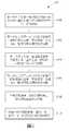
圖4是操作多晶片系統100的方法400的流程圖。該方法包含以下步驟:FIG. 4 is a flowchart of a
S400: 第一晶片20中的第一處理器26通過第一路徑向第一晶片20的第一存取控制器24產生第一控制訊號;S400: The
S402: 第一晶片20中的第一存取控制器24根據第一控制訊號產生第一存取訊號,以通過第二路徑存取非揮發性記憶體10;S402: The first access controller 24 in the
S404: 第二晶片30中的第二處理器36通過第三路徑向第二晶片30的第二存取控制器34產生第二控制訊號;S404: The
S406: 第二晶片30中的第二存取控制器34根據第二控制訊號產生第二存取訊號,以通過第四路徑存取非揮發性記憶體10;S406: The second access controller 34 in the
S408: 仲裁器22根據第一控制訊號和第二控制訊號產生仲裁訊號;及S408: The
S410: 根據仲裁訊號控制第一路徑,第二路徑,第三路徑及第四路徑的傳送。其中,第一晶片20與第二晶片30的操作係為各自獨立運作。S410: Control the transmission of the first path, the second path, the third path, and the fourth path according to the arbitration signal. Among them, the operations of the
綜上所述,本發明的多晶片系統及方法可共享單個非揮發性記憶體以實行晶片內執行指令,存儲資料,編程和擦除非揮發性記憶體以更新資料和指令,進而增加頻寬利用率。該多晶片系統及方法可以降低系統封裝的複雜性和成本,從而降低製造成本。以上所述僅為本發明之較佳實施例,凡依本發明申請專利範圍所做之均等變化與修飾,皆應屬本發明之涵蓋範圍。In summary, the multi-chip system and method of the present invention can share a single non-volatile memory to execute instructions within the chip, store data, and program and erase non-volatile memory to update data and instructions, thereby increasing bandwidth utilization rate. The multi-chip system and method can reduce the complexity and cost of system packaging, thereby reducing manufacturing costs.The above descriptions are only preferred embodiments of the present invention, and all equivalent changes and modifications made in accordance with the scope of the patent application of the present invention should fall within the scope of the present invention.
100:多晶片系統10:非揮發性記憶體20、30:晶片22:仲裁器21、31:匯流排26、36:處理器23、33:匯流排控制電路24、34:存取控制器25、35:輸入/輸出控制電路400:方法S400至S410:步驟ClkA:時脈訊號ReqA、ReqB:請求訊號GntA、GntB:授權訊號100: Multi-chip system10:
圖1是本發明實施例的多晶片系統的示意圖。圖2是仲裁過程操作訊號的示意圖。圖3是說明仲裁過程的狀態圖。圖4是操作圖1所述多晶片系統之方法的流程圖。Fig. 1 is a schematic diagram of a multi-chip system according to an embodiment of the present invention.Figure 2 is a schematic diagram of the operating signals of the arbitration process.Figure 3 is a state diagram illustrating the arbitration process.FIG. 4 is a flowchart of a method of operating the multi-chip system described in FIG. 1.
100:多晶片系統100: Multi-chip system
10:非揮發性記憶體10: Non-volatile memory
20、30:晶片20, 30: chip
22:仲裁器22: Arbiter
21、31:匯流排21, 31: busbar
26、36:處理器26, 36: processor
23、33:匯流排控制電路23, 33: bus control circuit
24、34:存取控制器24, 34: access controller
25、35:輸入/輸出控制電路25, 35: input/output control circuit
ReqA、ReqB:請求訊號ReqA, ReqB: request signal
GntA、GntB:授權訊號GntA, GntB: authorization signal
Claims (12)
Translated fromChineseApplications Claiming Priority (2)
| Application Number | Priority Date | Filing Date | Title |
|---|---|---|---|
| US16/459,548 | 2019-07-01 | ||
| US16/459,548US11157206B2 (en) | 2019-07-01 | 2019-07-01 | Multi-die system capable of sharing non-volatile memory |
Publications (2)
| Publication Number | Publication Date |
|---|---|
| TW202103012Atrue TW202103012A (en) | 2021-01-16 |
| TWI719622B TWI719622B (en) | 2021-02-21 |
Family
ID=69548132
Family Applications (1)
| Application Number | Title | Priority Date | Filing Date |
|---|---|---|---|
| TW108132106ATWI719622B (en) | 2019-07-01 | 2019-09-05 | Multi-die system |
Country Status (3)
| Country | Link |
|---|---|
| US (1) | US11157206B2 (en) |
| CN (1) | CN110825671A (en) |
| TW (1) | TWI719622B (en) |
Families Citing this family (3)
| Publication number | Priority date | Publication date | Assignee | Title |
|---|---|---|---|---|
| US11556248B2 (en)* | 2020-04-07 | 2023-01-17 | Micron Technology, Inc. | Apparatuses and methods for different burst lengths for stacked die |
| CN114690677B (en)* | 2020-12-31 | 2025-08-12 | 瑞昱新加坡有限公司 | Leakage current control of multi-chip module |
| JP2024000230A (en)* | 2022-06-20 | 2024-01-05 | 富士通株式会社 | Multiple die package |
Family Cites Families (12)
| Publication number | Priority date | Publication date | Assignee | Title |
|---|---|---|---|---|
| US6058459A (en)* | 1996-08-26 | 2000-05-02 | Stmicroelectronics, Inc. | Video/audio decompression/compression device including an arbiter and method for accessing a shared memory |
| US6691216B2 (en)* | 2000-11-08 | 2004-02-10 | Texas Instruments Incorporated | Shared program memory for use in multicore DSP devices |
| KR20020083589A (en)* | 2001-04-27 | 2002-11-04 | 현대네트웍스 주식회사 | Arbitration device to adsl code sharing in adsl subscriber board |
| WO2003009151A1 (en)* | 2001-07-18 | 2003-01-30 | Koninklijke Philips Electronics N.V. | Non-volatile memory arrangement and method in a multiprocessor device |
| US7107365B1 (en)* | 2002-06-25 | 2006-09-12 | Cypress Semiconductor Corp. | Early detection and grant, an arbitration scheme for single transfers on AMBA advanced high-performance bus |
| US6934782B2 (en)* | 2002-12-23 | 2005-08-23 | Lsi Logic Corporation | Process and apparatus for managing use of a peripheral bus among a plurality of controllers |
| US7447846B2 (en)* | 2006-04-12 | 2008-11-04 | Mediatek Inc. | Non-volatile memory sharing apparatus for multiple processors and method thereof |
| CN101075218A (en)* | 2007-07-18 | 2007-11-21 | 中兴通讯股份有限公司 | System for controlling data storage |
| TW201037707A (en)* | 2009-04-06 | 2010-10-16 | Himax Media Solutions Inc | Apparatus and methods for accessing memory units |
| US8296526B2 (en) | 2009-06-17 | 2012-10-23 | Mediatek, Inc. | Shared memory having multiple access configurations |
| US8407420B2 (en)* | 2010-06-23 | 2013-03-26 | International Business Machines Corporation | System, apparatus and method utilizing early access to shared cache pipeline for latency reduction |
| KR20150043045A (en)* | 2013-10-14 | 2015-04-22 | 에스케이하이닉스 주식회사 | Semiconductor device |
- 2019
- 2019-07-01USUS16/459,548patent/US11157206B2/enactiveActive
- 2019-09-05TWTW108132106Apatent/TWI719622B/enactive
- 2019-09-16CNCN201910871891.0Apatent/CN110825671A/enactivePending
Also Published As
| Publication number | Publication date |
|---|---|
| CN110825671A (en) | 2020-02-21 |
| US11157206B2 (en) | 2021-10-26 |
| TWI719622B (en) | 2021-02-21 |
| US20210004178A1 (en) | 2021-01-07 |
Similar Documents
| Publication | Publication Date | Title |
|---|---|---|
| TWI719622B (en) | Multi-die system | |
| US7752373B2 (en) | System and method for controlling memory operations | |
| US11256651B2 (en) | Multiple master, multi-slave serial peripheral interface | |
| EP2548127B1 (en) | Requests and data handling in a bus architecture | |
| CN103197966B (en) | Semiconductors data processing equipment, time triggered communication system and communication system | |
| US7769936B2 (en) | Data processing apparatus and method for arbitrating between messages routed over a communication channel | |
| US10511455B1 (en) | Time sensitive networking control circuitry | |
| WO2019152716A1 (en) | End-to-end quality-of-service in a network-on-chip | |
| US7698524B2 (en) | Apparatus and methods for controlling output of clock signal and systems including the same | |
| US20110213903A1 (en) | Pin Multiplexing | |
| US9003092B2 (en) | System on chip bus system and a method of operating the bus system | |
| JPH06231074A (en) | Multiple access system for system bus | |
| TWI750118B (en) | Clock management circuitry, system on chip and method of clock management | |
| US5548797A (en) | Digital clock pulse positioning circuit for delaying a signal input by a fist time duration and a second time duration to provide a positioned clock signal | |
| JP7226084B2 (en) | Information processing equipment | |
| JP7259537B2 (en) | Information processing equipment | |
| CN107621974B (en) | Interrupt request distribution device and method for operating same | |
| JP6725970B2 (en) | Multiprocessor system | |
| KR100666950B1 (en) | Multiple Memory Access System and Method for Packet Processing | |
| JP2013122713A (en) | Semiconductor device | |
| JPS5953923A (en) | Data processing system | |
| GB2488680A (en) | A method/architecture for processing requests in a bus architecture that includes at least two master devices an at least one slave device | |
| JP2002169769A (en) | Bus master and bus mediating system | |
| JP2002007310A (en) | Semiconductor device | |
| JP2016170751A (en) | Transfer control circuit and transfer control method |