TW202102883A - Directional display apparatus - Google Patents
Directional display apparatusDownload PDFInfo
- Publication number
- TW202102883A TW202102883ATW109122033ATW109122033ATW202102883ATW 202102883 ATW202102883 ATW 202102883ATW 109122033 ATW109122033 ATW 109122033ATW 109122033 ATW109122033 ATW 109122033ATW 202102883 ATW202102883 ATW 202102883A
- Authority
- TW
- Taiwan
- Prior art keywords
- display device
- light
- parallax barrier
- retarder
- polarizer
- Prior art date
Links
- 230000004888barrier functionEffects0.000claimsabstractdescription333
- 230000003287optical effectEffects0.000claimsabstractdescription93
- 230000005540biological transmissionEffects0.000claimsabstractdescription54
- 238000005286illuminationMethods0.000claimsabstractdescription40
- 230000010287polarizationEffects0.000claimsdescription293
- 238000002834transmittanceMethods0.000claimsdescription136
- 239000000463materialSubstances0.000claimsdescription120
- 239000004973liquid crystal related substanceSubstances0.000claimsdescription99
- 238000010521absorption reactionMethods0.000claimsdescription30
- 230000010363phase shiftEffects0.000claimsdescription30
- 238000005538encapsulationMethods0.000claimsdescription27
- 230000007613environmental effectEffects0.000claimsdescription27
- 229910001111Fine metalInorganic materials0.000claimsdescription20
- 238000000034methodMethods0.000claimsdescription19
- QVGXLLKOCUKJST-UHFFFAOYSA-Natomic oxygenChemical compound[O]QVGXLLKOCUKJST-UHFFFAOYSA-N0.000claimsdescription16
- 229910052760oxygenInorganic materials0.000claimsdescription16
- 239000001301oxygenSubstances0.000claimsdescription16
- XLYOFNOQVPJJNP-UHFFFAOYSA-NwaterSubstancesOXLYOFNOQVPJJNP-UHFFFAOYSA-N0.000claimsdescription16
- 239000011148porous materialSubstances0.000claimsdescription15
- 239000011358absorbing materialSubstances0.000claimsdescription10
- 238000002835absorbanceMethods0.000claimsdescription6
- 238000001459lithographyMethods0.000claimsdescription6
- 238000000059patterningMethods0.000claimsdescription5
- 229910010272inorganic materialInorganic materials0.000claimsdescription4
- 239000011147inorganic materialSubstances0.000claimsdescription4
- 238000002310reflectometryMethods0.000abstractdescription64
- 230000003595spectral effectEffects0.000abstractdescription26
- 239000010410layerSubstances0.000description235
- 238000009826distributionMethods0.000description132
- 238000010586diagramMethods0.000description105
- 230000000007visual effectEffects0.000description72
- 230000002829reductive effectEffects0.000description38
- 230000031700light absorptionEffects0.000description35
- 239000000758substrateSubstances0.000description31
- 230000008859changeEffects0.000description27
- 230000009467reductionEffects0.000description11
- 239000011521glassSubstances0.000description10
- 125000006850spacer groupChemical group0.000description10
- 230000000694effectsEffects0.000description9
- 239000000945fillerSubstances0.000description9
- 238000004519manufacturing processMethods0.000description9
- 210000002858crystal cellAnatomy0.000description8
- 239000010408filmSubstances0.000description8
- 238000010561standard procedureMethods0.000description8
- 230000006870functionEffects0.000description7
- 230000001902propagating effectEffects0.000description6
- 210000001747pupilAnatomy0.000description6
- 238000006243chemical reactionMethods0.000description5
- 230000027756respiratory electron transport chainEffects0.000description5
- 238000012546transferMethods0.000description5
- 230000001154acute effectEffects0.000description4
- 239000000853adhesiveSubstances0.000description4
- 230000001070adhesive effectEffects0.000description4
- 238000003491arrayMethods0.000description4
- 230000007423decreaseEffects0.000description4
- 238000003384imaging methodMethods0.000description4
- 239000012044organic layerSubstances0.000description4
- 238000000206photolithographyMethods0.000description4
- 238000007639printingMethods0.000description4
- 230000035945sensitivityEffects0.000description4
- 238000001228spectrumMethods0.000description4
- 239000000126substanceSubstances0.000description4
- 239000004985Discotic Liquid Crystal SubstanceSubstances0.000description3
- 230000008901benefitEffects0.000description3
- 238000013461designMethods0.000description3
- 238000002474experimental methodMethods0.000description3
- 238000005259measurementMethods0.000description3
- 238000005498polishingMethods0.000description3
- 230000002441reversible effectEffects0.000description3
- 239000010409thin filmSubstances0.000description3
- YBJHBAHKTGYVGT-ZKWXMUAHSA-N(+)-BiotinChemical compoundN1C(=O)N[C@@H]2[C@H](CCCCC(=O)O)SC[C@@H]21YBJHBAHKTGYVGT-ZKWXMUAHSA-N0.000description2
- 230000002159abnormal effectEffects0.000description2
- 230000015572biosynthetic processEffects0.000description2
- 239000003990capacitorSubstances0.000description2
- 230000003098cholesteric effectEffects0.000description2
- 239000003086colorantSubstances0.000description2
- 229910003460diamondInorganic materials0.000description2
- 239000010432diamondSubstances0.000description2
- 230000005684electric fieldEffects0.000description2
- 230000005525hole transportEffects0.000description2
- 229910052751metalInorganic materials0.000description2
- 239000002184metalSubstances0.000description2
- 230000004048modificationEffects0.000description2
- 238000012986modificationMethods0.000description2
- 229920000515polycarbonatePolymers0.000description2
- 239000004417polycarbonateSubstances0.000description2
- 230000001681protective effectEffects0.000description2
- 230000005855radiationEffects0.000description2
- 239000004065semiconductorSubstances0.000description2
- 238000000926separation methodMethods0.000description2
- 238000004088simulationMethods0.000description2
- 239000007787solidSubstances0.000description2
- FEPMHVLSLDOMQC-UHFFFAOYSA-Nvirginiamycin-S1Natural productsCC1OC(=O)C(C=2C=CC=CC=2)NC(=O)C2CC(=O)CCN2C(=O)C(CC=2C=CC=CC=2)N(C)C(=O)C2CCCN2C(=O)C(CC)NC(=O)C1NC(=O)C1=NC=CC=C1OFEPMHVLSLDOMQC-UHFFFAOYSA-N0.000description2
- 229910002651NO3Inorganic materials0.000description1
- 239000004988Nematic liquid crystalSubstances0.000description1
- NHNBFGGVMKEFGY-UHFFFAOYSA-NNitrateChemical compound[O-][N+]([O-])=ONHNBFGGVMKEFGY-UHFFFAOYSA-N0.000description1
- BQCADISMDOOEFD-UHFFFAOYSA-NSilverChemical compound[Ag]BQCADISMDOOEFD-UHFFFAOYSA-N0.000description1
- 230000015556catabolic processEffects0.000description1
- 230000001427coherent effectEffects0.000description1
- 230000002301combined effectEffects0.000description1
- 238000012937correctionMethods0.000description1
- 230000003247decreasing effectEffects0.000description1
- 238000006731degradation reactionMethods0.000description1
- 230000000593degrading effectEffects0.000description1
- 239000002019doping agentSubstances0.000description1
- 238000005516engineering processMethods0.000description1
- 238000005530etchingMethods0.000description1
- 210000003128headAnatomy0.000description1
- 230000005764inhibitory processEffects0.000description1
- 238000007641inkjet printingMethods0.000description1
- 238000007689inspectionMethods0.000description1
- 230000001678irradiating effectEffects0.000description1
- 238000002955isolationMethods0.000description1
- 230000000873masking effectEffects0.000description1
- 230000007246mechanismEffects0.000description1
- 239000000203mixtureSubstances0.000description1
- 239000012788optical filmSubstances0.000description1
- 238000001579optical reflectometryMethods0.000description1
- 239000011368organic materialSubstances0.000description1
- 230000002093peripheral effectEffects0.000description1
- 239000002861polymer materialSubstances0.000description1
- 230000008569processEffects0.000description1
- 238000011084recoveryMethods0.000description1
- 238000009877renderingMethods0.000description1
- 230000004044responseEffects0.000description1
- 229910052709silverInorganic materials0.000description1
- 239000004332silverSubstances0.000description1
- 239000002356single layerSubstances0.000description1
- 230000001629suppressionEffects0.000description1
- 230000009466transformationEffects0.000description1
Images


Classifications
- G—PHYSICS
- G02—OPTICS
- G02F—OPTICAL DEVICES OR ARRANGEMENTS FOR THE CONTROL OF LIGHT BY MODIFICATION OF THE OPTICAL PROPERTIES OF THE MEDIA OF THE ELEMENTS INVOLVED THEREIN; NON-LINEAR OPTICS; FREQUENCY-CHANGING OF LIGHT; OPTICAL LOGIC ELEMENTS; OPTICAL ANALOGUE/DIGITAL CONVERTERS
- G02F1/00—Devices or arrangements for the control of the intensity, colour, phase, polarisation or direction of light arriving from an independent light source, e.g. switching, gating or modulating; Non-linear optics
- G02F1/01—Devices or arrangements for the control of the intensity, colour, phase, polarisation or direction of light arriving from an independent light source, e.g. switching, gating or modulating; Non-linear optics for the control of the intensity, phase, polarisation or colour
- G02F1/13—Devices or arrangements for the control of the intensity, colour, phase, polarisation or direction of light arriving from an independent light source, e.g. switching, gating or modulating; Non-linear optics for the control of the intensity, phase, polarisation or colour based on liquid crystals, e.g. single liquid crystal display cells
- G02F1/133—Constructional arrangements; Operation of liquid crystal cells; Circuit arrangements
- G02F1/1333—Constructional arrangements; Manufacturing methods
- G02F1/1335—Structural association of cells with optical devices, e.g. polarisers or reflectors
- G02F1/133528—Polarisers
- H—ELECTRICITY
- H04—ELECTRIC COMMUNICATION TECHNIQUE
- H04N—PICTORIAL COMMUNICATION, e.g. TELEVISION
- H04N13/00—Stereoscopic video systems; Multi-view video systems; Details thereof
- H04N13/30—Image reproducers
- H04N13/302—Image reproducers for viewing without the aid of special glasses, i.e. using autostereoscopic displays
- H04N13/31—Image reproducers for viewing without the aid of special glasses, i.e. using autostereoscopic displays using parallax barriers
- H04N13/315—Image reproducers for viewing without the aid of special glasses, i.e. using autostereoscopic displays using parallax barriers the parallax barriers being time-variant
- G—PHYSICS
- G02—OPTICS
- G02F—OPTICAL DEVICES OR ARRANGEMENTS FOR THE CONTROL OF LIGHT BY MODIFICATION OF THE OPTICAL PROPERTIES OF THE MEDIA OF THE ELEMENTS INVOLVED THEREIN; NON-LINEAR OPTICS; FREQUENCY-CHANGING OF LIGHT; OPTICAL LOGIC ELEMENTS; OPTICAL ANALOGUE/DIGITAL CONVERTERS
- G02F1/00—Devices or arrangements for the control of the intensity, colour, phase, polarisation or direction of light arriving from an independent light source, e.g. switching, gating or modulating; Non-linear optics
- G02F1/01—Devices or arrangements for the control of the intensity, colour, phase, polarisation or direction of light arriving from an independent light source, e.g. switching, gating or modulating; Non-linear optics for the control of the intensity, phase, polarisation or colour
- G02F1/13—Devices or arrangements for the control of the intensity, colour, phase, polarisation or direction of light arriving from an independent light source, e.g. switching, gating or modulating; Non-linear optics for the control of the intensity, phase, polarisation or colour based on liquid crystals, e.g. single liquid crystal display cells
- G02F1/1323—Arrangements for providing a switchable viewing angle
- G—PHYSICS
- G02—OPTICS
- G02F—OPTICAL DEVICES OR ARRANGEMENTS FOR THE CONTROL OF LIGHT BY MODIFICATION OF THE OPTICAL PROPERTIES OF THE MEDIA OF THE ELEMENTS INVOLVED THEREIN; NON-LINEAR OPTICS; FREQUENCY-CHANGING OF LIGHT; OPTICAL LOGIC ELEMENTS; OPTICAL ANALOGUE/DIGITAL CONVERTERS
- G02F1/00—Devices or arrangements for the control of the intensity, colour, phase, polarisation or direction of light arriving from an independent light source, e.g. switching, gating or modulating; Non-linear optics
- G02F1/01—Devices or arrangements for the control of the intensity, colour, phase, polarisation or direction of light arriving from an independent light source, e.g. switching, gating or modulating; Non-linear optics for the control of the intensity, phase, polarisation or colour
- G02F1/13—Devices or arrangements for the control of the intensity, colour, phase, polarisation or direction of light arriving from an independent light source, e.g. switching, gating or modulating; Non-linear optics for the control of the intensity, phase, polarisation or colour based on liquid crystals, e.g. single liquid crystal display cells
- G02F1/133—Constructional arrangements; Operation of liquid crystal cells; Circuit arrangements
- G02F1/1333—Constructional arrangements; Manufacturing methods
- G02F1/13338—Input devices, e.g. touch panels
- G—PHYSICS
- G02—OPTICS
- G02F—OPTICAL DEVICES OR ARRANGEMENTS FOR THE CONTROL OF LIGHT BY MODIFICATION OF THE OPTICAL PROPERTIES OF THE MEDIA OF THE ELEMENTS INVOLVED THEREIN; NON-LINEAR OPTICS; FREQUENCY-CHANGING OF LIGHT; OPTICAL LOGIC ELEMENTS; OPTICAL ANALOGUE/DIGITAL CONVERTERS
- G02F1/00—Devices or arrangements for the control of the intensity, colour, phase, polarisation or direction of light arriving from an independent light source, e.g. switching, gating or modulating; Non-linear optics
- G02F1/01—Devices or arrangements for the control of the intensity, colour, phase, polarisation or direction of light arriving from an independent light source, e.g. switching, gating or modulating; Non-linear optics for the control of the intensity, phase, polarisation or colour
- G02F1/13—Devices or arrangements for the control of the intensity, colour, phase, polarisation or direction of light arriving from an independent light source, e.g. switching, gating or modulating; Non-linear optics for the control of the intensity, phase, polarisation or colour based on liquid crystals, e.g. single liquid crystal display cells
- G02F1/133—Constructional arrangements; Operation of liquid crystal cells; Circuit arrangements
- G02F1/1333—Constructional arrangements; Manufacturing methods
- G02F1/1335—Structural association of cells with optical devices, e.g. polarisers or reflectors
- G02F1/133553—Reflecting elements
- H—ELECTRICITY
- H10—SEMICONDUCTOR DEVICES; ELECTRIC SOLID-STATE DEVICES NOT OTHERWISE PROVIDED FOR
- H10K—ORGANIC ELECTRIC SOLID-STATE DEVICES
- H10K50/00—Organic light-emitting devices
- H10K50/80—Constructional details
- H10K50/86—Arrangements for improving contrast, e.g. preventing reflection of ambient light
- H10K50/865—Arrangements for improving contrast, e.g. preventing reflection of ambient light comprising light absorbing layers, e.g. light-blocking layers
- H—ELECTRICITY
- H10—SEMICONDUCTOR DEVICES; ELECTRIC SOLID-STATE DEVICES NOT OTHERWISE PROVIDED FOR
- H10K—ORGANIC ELECTRIC SOLID-STATE DEVICES
- H10K59/00—Integrated devices, or assemblies of multiple devices, comprising at least one organic light-emitting element covered by group H10K50/00
- H10K59/40—OLEDs integrated with touch screens
- H—ELECTRICITY
- H10—SEMICONDUCTOR DEVICES; ELECTRIC SOLID-STATE DEVICES NOT OTHERWISE PROVIDED FOR
- H10K—ORGANIC ELECTRIC SOLID-STATE DEVICES
- H10K59/00—Integrated devices, or assemblies of multiple devices, comprising at least one organic light-emitting element covered by group H10K50/00
- H10K59/50—OLEDs integrated with light modulating elements, e.g. with electrochromic elements, photochromic elements or liquid crystal elements
- H—ELECTRICITY
- H10—SEMICONDUCTOR DEVICES; ELECTRIC SOLID-STATE DEVICES NOT OTHERWISE PROVIDED FOR
- H10K—ORGANIC ELECTRIC SOLID-STATE DEVICES
- H10K59/00—Integrated devices, or assemblies of multiple devices, comprising at least one organic light-emitting element covered by group H10K50/00
- H10K59/80—Constructional details
- H10K59/8791—Arrangements for improving contrast, e.g. preventing reflection of ambient light
- H10K59/8792—Arrangements for improving contrast, e.g. preventing reflection of ambient light comprising light absorbing layers, e.g. black layers
- H—ELECTRICITY
- H10—SEMICONDUCTOR DEVICES; ELECTRIC SOLID-STATE DEVICES NOT OTHERWISE PROVIDED FOR
- H10K—ORGANIC ELECTRIC SOLID-STATE DEVICES
- H10K71/00—Manufacture or treatment specially adapted for the organic devices covered by this subclass
- G—PHYSICS
- G02—OPTICS
- G02B—OPTICAL ELEMENTS, SYSTEMS OR APPARATUS
- G02B2207/00—Coding scheme for general features or characteristics of optical elements and systems of subclass G02B, but not including elements and systems which would be classified in G02B6/00 and subgroups
- G02B2207/123—Optical louvre elements, e.g. for directional light blocking
- G—PHYSICS
- G02—OPTICS
- G02F—OPTICAL DEVICES OR ARRANGEMENTS FOR THE CONTROL OF LIGHT BY MODIFICATION OF THE OPTICAL PROPERTIES OF THE MEDIA OF THE ELEMENTS INVOLVED THEREIN; NON-LINEAR OPTICS; FREQUENCY-CHANGING OF LIGHT; OPTICAL LOGIC ELEMENTS; OPTICAL ANALOGUE/DIGITAL CONVERTERS
- G02F1/00—Devices or arrangements for the control of the intensity, colour, phase, polarisation or direction of light arriving from an independent light source, e.g. switching, gating or modulating; Non-linear optics
- G02F1/01—Devices or arrangements for the control of the intensity, colour, phase, polarisation or direction of light arriving from an independent light source, e.g. switching, gating or modulating; Non-linear optics for the control of the intensity, phase, polarisation or colour
- G02F1/13—Devices or arrangements for the control of the intensity, colour, phase, polarisation or direction of light arriving from an independent light source, e.g. switching, gating or modulating; Non-linear optics for the control of the intensity, phase, polarisation or colour based on liquid crystals, e.g. single liquid crystal display cells
- G02F1/133—Constructional arrangements; Operation of liquid crystal cells; Circuit arrangements
- G02F1/1333—Constructional arrangements; Manufacturing methods
- G02F1/1335—Structural association of cells with optical devices, e.g. polarisers or reflectors
- G02F1/133528—Polarisers
- G02F1/133531—Polarisers characterised by the arrangement of polariser or analyser axes
Landscapes
- Physics & Mathematics (AREA)
- Nonlinear Science (AREA)
- Optics & Photonics (AREA)
- Chemical & Material Sciences (AREA)
- Crystallography & Structural Chemistry (AREA)
- General Physics & Mathematics (AREA)
- Mathematical Physics (AREA)
- Engineering & Computer Science (AREA)
- Multimedia (AREA)
- Signal Processing (AREA)
- Manufacturing & Machinery (AREA)
- Devices For Indicating Variable Information By Combining Individual Elements (AREA)
- Electroluminescent Light Sources (AREA)
- Liquid Crystal (AREA)
Abstract
Description
Translated fromChinese本揭示案大體上涉及來自光調變裝置之照射,且更具體而言涉及用於包括私密顯示器及夜間顯示器之顯示器中的用於提供照射控制之光學堆疊。The present disclosure generally relates to illumination from light modulating devices, and more specifically to optical stacks for providing illumination control in displays including private displays and night displays.
私密顯示器向通常在同軸位置上之主要使用者提供影像可見性,且降低對通常在離軸位置上的窺探者之影像內容可見性。可由微窗光學膜提供私密功能,該等光學膜在離軸位置中以低亮度透射來自同軸方向上之顯示器的一些光。然而,此類膜對於正面照射具有高損耗,且由於空間光調變器之像素的跳動,微窗可能會引起穆爾偽像。微窗之間距可能需要選擇面板解析度,從而增大了庫存及成本。The private display provides image visibility to the primary user who is usually in the coaxial position, and reduces the visibility of the image content to the prying person who is usually in the off-axis position. The privacy function can be provided by the micro-window optical film, which transmits some light from the display in the coaxial direction with low brightness in the off-axis position. However, this type of film has high loss for front-side illumination, and due to the jitter of the pixels of the spatial light modulator, the micro-window may cause Moore artifacts. The distance between the micro windows may need to select the panel resolution, which increases inventory and costs.
可藉由控制離軸光學輸出來提供可切換私密顯示器。A switchable private display can be provided by controlling the off-axis optical output.
可藉助於降低亮度來提供控制,例如藉助於用於液晶顯示器(LCD)空間光調變器之可切換背光來提供控制。顯示器背光大體上採用波導及邊緣發射源。某些成像定向背光具有將照射通過顯示面板引導至檢視窗的額外能力。成像系統可形成於多個源與各別窗影像之間。成像定向背光之一個實例為可採用摺疊式光學系統之光閥,且因此亦可為摺疊式成像定向背光之實例。如美國專利第9,519,153號中所描述,光可大體上在一個方向上無損地傳播通過光閥,而可藉由反射離開傾斜刻面來提取反向傳播的光,該專利以全文引用之方式併入本文中。Control can be provided by reducing the brightness, for example by a switchable backlight used in a liquid crystal display (LCD) spatial light modulator. The display backlight generally uses waveguide and edge emission sources. Certain imaging directional backlights have the additional ability to direct illumination through the display panel to the viewing window. The imaging system can be formed between multiple sources and individual window images. An example of an imaging directional backlight is a light valve that can employ a folding optical system, and therefore can also be an example of a folding imaging directional backlight. As described in U.S. Patent No. 9,519,153, light can propagate through the light valve substantially without loss in one direction, and the back-propagating light can be extracted by reflecting off the inclined facet. The patent is incorporated by reference in its entirety. Into this article.
根據本揭示案之第一態樣,提供一種顯示裝置,其包含:發射式空間光調變器,其包含配置於像素層中之像素陣列;視差障壁,其形成孔隙陣列,其中視差障壁沿著一軸線與像素層分離一視差距離,該軸線沿著像素層之平面的法線;每一像素與孔隙對準。視差障壁可將來自每一像素之光引導至共同檢視窗中。有利地,可實現具有低反射率且降低之離軸亮度的全解析度影像。According to the first aspect of the present disclosure, there is provided a display device, which includes: an emissive spatial light modulator including a pixel array arranged in a pixel layer; and a parallax barrier, which forms an array of apertures, wherein the parallax barrier is along the An axis is separated from the pixel layer by a parallax distance, and the axis is along the normal to the plane of the pixel layer; each pixel is aligned with the aperture. The parallax barrier can guide the light from each pixel to the common viewing window. Advantageously, a full-resolution image with low reflectivity and reduced off-axis brightness can be realized.
沿著孔隙最接近之方向,孔隙之寬度a及像素之寬度w可滿足如下要求:a
沿著孔隙最接近之方向,孔隙之寬度a、像素之間距p,以及像素之寬度w可滿足如下要求:a
視差障壁距像素之間隔d、像素沿著孔隙最接近之方向的間距p,以及視差障壁與像素之間的材料之折射率n可滿足如下要求:2d/p
視差障壁距像素之間隔d、孔隙沿著孔隙最接近之方向的寬度a,以及視差障壁與像素之間的材料之折射率n可滿足如下要求:d
視差障壁距像素之間隔d、孔隙沿著孔隙最接近之方向的寬度a,以及視差障壁與像素之間的材料之折射率n可滿足如下要求:d
沿著孔隙最接近之方向的間距p’可小於各別經對準像素沿著像素最接近之方向的間距p;且檢視窗可形成於在空間光調變器之輸出側上的檢視窗平面處。有利地,對於正面顯示器使用者,增大了亮度均勻性。Direction along the pitchp of the aperture closest'may be less than the respective pixels aligned along the direction of the closest pixel pitchp; subject window and the window may be formed in the object plane on the output side of the spatial light modulator of the Place. Advantageously, for front display users, the brightness uniformity is increased.
視差障壁可形成二維孔隙陣列,每一像素與各別孔隙對準。可針對側角及仰角實現亮度降低。有利地,私密顯示器可具備橫向及縱向私密操作。可降低顯示器反射率且增大正面方向上的顯示器效率。The parallax barrier can form a two-dimensional array of apertures, with each pixel aligned with a separate aperture. Brightness reduction can be achieved for side angles and elevation angles. Advantageously, the private display can have horizontal and vertical private operations. The reflectivity of the display can be reduced and the display efficiency in the front direction can be increased.
像素可按行及列配置,孔隙最接近之方向可相對於輸出線性偏振器之電向量透射方向成45度;且每一像素可具有為正方形形狀之發光區,發光區之邊緣相對於輸出線性偏振器之電向量透射方向旋轉45度。孔隙可具有邊緣相對於輸出線性偏振器之電向量透射方向旋轉45度之正方形形狀;或孔隙可具有圓形形狀。有利地,可沿著側向及仰角方位方向實現高極角下的均勻亮度衰減及亮度降低。Pixels can be arranged in rows and columns. The closest direction of the aperture can be 45 degrees with respect to the transmission direction of the electric vector of the output linear polarizer; and each pixel can have a square-shaped light-emitting area, and the edge of the light-emitting area is linear with respect to the output The transmission direction of the electric vector of the polarizer is rotated by 45 degrees. The aperture may have a square shape with an edge rotated by 45 degrees with respect to the transmission direction of the electric vector of the output linear polarizer; or the aperture may have a circular shape. Advantageously, uniform brightness attenuation and brightness reduction at high polar angles can be achieved along the lateral and elevation azimuth directions.
對於像素中之至少一些,發光區可包含發光子區及非發光子區。對於紅色、綠色以及藍色像素,發光子區與非發光區之面積比可不同。可以類似驅動電壓驅動彩色像素,以實現與其中未設置視差障壁之顯示器中所提供之亮度匹配的輸出亮度。有利地,控制及驅動器電子器件降低了複雜度且增大了效率。For at least some of the pixels, the light-emitting region may include light-emitting sub-regions and non-light-emitting sub-regions. For red, green, and blue pixels, the area ratio of the light-emitting sub-region and the non-light-emitting region may be different. The color pixels can be driven similarly to the driving voltage to achieve output brightness that matches the brightness provided in the display in which the parallax barrier is not provided. Advantageously, control and driver electronics reduce complexity and increase efficiency.
視差障壁可形成一維孔隙陣列,像素按行配置,每一行像素與各別孔隙對準。可減少對像素配置之修改,從而降低成本。每一像素可具有在孔隙延伸之方向上延伸的發光區;對於像素中之每一者,紅色、綠色以及藍色發光區之寬度可相同;且對於紅色、綠色以及藍色發光像素,發光區之高度可不同。顯示器可便利地在一個方向上繞一軸線旋轉,以有利地為正面觀察者提供舒適檢視高度。視差障壁之產量及對準成本可降低。The parallax barrier can form a one-dimensional array of apertures, pixels are arranged in rows, and each row of pixels is aligned with a separate aperture. It can reduce the modification of the pixel configuration, thereby reducing the cost. Each pixel may have a light-emitting area extending in the direction in which the aperture extends; for each of the pixels, the width of the red, green, and blue light-emitting areas may be the same; and for the red, green, and blue light-emitting pixels, the light-emitting area The height can be different. The display can be conveniently rotated around an axis in one direction to advantageously provide a comfortable viewing height for frontal observers. The production and alignment costs of the parallax barrier can be reduced.
視差障壁可經配置以吸收入射於其上的光。可減少顯示器反射,從而有利地增大明亮環境中之顯示器對比度。The parallax barrier may be configured to absorb light incident thereon. It can reduce the display reflection, thereby advantageously increasing the contrast of the display in a bright environment.
在孔隙之間的視差障壁區之吸收率可小於100%,且可大於80%,較佳地大於90%,且更佳地大於95%。相比於吸收區中具備100%吸收率之視差障壁,顯示器之離軸影像可見性可被增大。The absorption rate of the parallax barrier region between the apertures may be less than 100%, and may be greater than 80%, preferably greater than 90%, and more preferably greater than 95%. Compared with the parallax barrier with 100% absorption in the absorption zone, the visibility of the off-axis image of the display can be increased.
顯示裝置可用於環境照射中,且視差障壁可吸收自像素層反射開的透射通過孔隙之環境照射中之至少一些。反射被減少,從而有利地增大了觀察到之影像對比度。The display device can be used in environmental illumination, and the parallax barrier can absorb at least some of the environmental illumination reflected from the pixel layer and transmitted through the aperture. The reflection is reduced, which advantageously increases the contrast of the observed image.
顯示裝置可具有介於像素層與視差障壁之間的一或多個額外層,其中像素、一或多個額外層以及視差障壁可形成為單塊堆疊。有利地,像素層與視差障壁層之分離在施加機械力期間可具備高穩定性。The display device may have one or more additional layers between the pixel layer and the parallax barrier, where the pixels, the one or more additional layers, and the parallax barrier may be formed as a monolithic stack. Advantageously, the separation of the pixel layer and the parallax barrier layer can have high stability during the application of mechanical force.
一或多個額外層可包含配置成提供對水及氧氣之障壁的至少一個透光無機層。視差障壁可包含配置成提供對水及氧氣之障壁的至少一種透光無機材料。視差障壁可配置於像素層與至少一個透光無機層之間,該透光無機層可經配置以提供對水及氧氣之障壁。有利地,可增大顯示器之壽命。The one or more additional layers may include at least one light-transmitting inorganic layer configured to provide a barrier to water and oxygen. The parallax barrier may include at least one light-transmitting inorganic material configured to provide a barrier to water and oxygen. The parallax barrier may be disposed between the pixel layer and the at least one light-transmitting inorganic layer, and the light-transmitting inorganic layer may be configured to provide a barrier to water and oxygen. Advantageously, the life span of the display can be increased.
輸出偏振器可配置於空間光調變器之輸出上,輸出偏振器為線性偏振器;且反射控制四分之一波長延遲器可配置於輸出偏振器與空間光調變器之間。有利地,可減少來自像素層之反射。The output polarizer can be arranged on the output of the spatial light modulator, and the output polarizer is a linear polarizer; and the reflection control quarter-wave retarder can be arranged between the output polarizer and the spatial light modulator. Advantageously, reflection from the pixel layer can be reduced.
視差障壁可配置於像素層與反射控制四分之一波長延遲器之間。有利地,可便利地實現像素層與視差障壁之間的較小間隔。The parallax barrier can be arranged between the pixel layer and the reflection control quarter-wave retarder. Advantageously, a small interval between the pixel layer and the parallax barrier can be conveniently realized.
顯示裝置可進一步包含配置於輸出偏振器之輸出側上的額外偏振器,額外偏振器為線性偏振器;且至少一個偏振控制延遲器配置於輸出偏振器與額外偏振器之間。可提供有利地具有高視覺安全等級之私密顯示器。The display device may further include an additional polarizer disposed on the output side of the output polarizer, the additional polarizer is a linear polarizer; and at least one polarization control retarder is disposed between the output polarizer and the additional polarizer. It is possible to provide a private display which advantageously has a high visual security level.
當輸出偏振器及額外偏振器中之至少一者與相同材料之假想偏振器交叉時,相比在自450nm至490nm之波長下的透射率,輸出偏振器及額外偏振器中之至少一者在自520nm至560nm之波長下的透射率可較小。在自450nm至490nm之波長下,透射率可大於1%,較佳地大於2%,且最佳地大於3%;且在自520nm至560nm之波長下,透射率可小於3%,較佳地小於2%,且最佳地小於1%。相比於寬頻帶吸收式偏振器,顯示器之透射率可被增大。有利地,增大了顯示器效率。對於藍色波長,透射率可相對較大。有利地,可增大顯示器之壽命。When at least one of the output polarizer and the additional polarizer crosses an imaginary polarizer of the same material, at least one of the output polarizer and the additional polarizer is higher than the transmittance at a wavelength from 450nm to 490nm The transmittance at wavelengths from 520nm to 560nm can be small. At a wavelength from 450nm to 490nm, the transmittance can be greater than 1%, preferably greater than 2%, and most preferably greater than 3%; and at a wavelength from 520nm to 560nm, the transmittance can be less than 3%, preferably The ground is less than 2%, and optimally less than 1%. Compared with a broadband absorptive polarizer, the transmittance of the display can be increased. Advantageously, the display efficiency is increased. For blue wavelengths, the transmittance can be relatively large. Advantageously, the life span of the display can be increased.
至少一個偏振控制延遲器可進一步包含至少一個被動延遲器。The at least one polarization control retarder may further include at least one passive retarder.
至少一個偏振控制延遲器可能夠同時進行以下操作:不向由輸出偏振器沿著一軸線傳遞之光的正交偏振分量引入淨相對相移,該軸線沿著至少一個偏振控制延遲器之平面的法線;及向由反射性偏振器沿著一軸線傳遞之光的正交偏振分量引入相對相移,該軸線傾斜於至少一個偏振控制延遲器之平面的法線。至少一個被動延遲器可包含其光軸垂直於延遲器之平面的延遲器,對於550nm之波長的光,至少一個被動延遲器具有介於-150 nm至-900 nm之範圍內,較佳地介於-200nm至-500nm之範圍內,且最佳地介於-250 nm至-400nm之範圍內的延遲。可實現具有降低之亮度的較大離軸極座標區。有利地,對於許多窺探者位置,視覺安全等級較高。At least one polarization control retarder may be capable of simultaneously performing the following operations: not introducing a net relative phase shift to the orthogonal polarization components of the light transmitted by the output polarizer along an axis that is along the plane of the at least one polarization control retarder Normal; and introducing a relative phase shift to the orthogonal polarization component of the light transmitted by the reflective polarizer along an axis that is inclined to the normal to the plane of the at least one polarization control retarder. At least one passive retarder may include a retarder whose optical axis is perpendicular to the plane of the retarder. For light with a wavelength of 550 nm, at least one passive retarder has a range between -150 nm and -900 nm, preferably between -150 nm and -900 nm. Retardation in the range of -200nm to -500nm, and optimally in the range of -250nm to -400nm. A larger off-axis polar coordinate area with reduced brightness can be realized. Advantageously, for many snooper locations, the level of visual security is higher.
至少一個延遲器可包含:配置於額外偏振器與輸出偏振器之間的第一及第二四分之一波片,第一四分之一波片配置於第二四分之一波片之輸入側上,且配置成將由其輸入側上之輸出偏振器傳遞的經線性偏振之偏振狀態轉換成經圓形偏振之偏振狀態,且輸出側上的第二四分之一波片配置成將入射於其上的經圓形偏振之偏振狀態轉換成由其輸出側上的額外偏振器傳遞的經線性偏振之偏振狀態;及配置於該對四分之一波片之間的至少一個延遲器。配置於該對四分之一波片之間的延遲器可包含其光軸垂直於延遲器之平面的延遲器,對於550nm之波長的光,至少一個被動延遲器具有介於-150 nm至-500nm之範圍內,較佳地介於-200nm至-400nm之範圍內,且最佳地介於-250 nm至-350nm之範圍內的延遲。可提供旋轉對稱之極座標亮度減少分佈。有利地,私密顯示器可在橫向及縱向模式下操作。對於自使用者頭部上方俯視之窺探者,可實現高視覺安全性。The at least one retarder may include: first and second quarter wave plates arranged between the additional polarizer and the output polarizer, the first quarter wave plate being arranged between the second quarter wave plate On the input side and configured to convert the linearly polarized polarization state transmitted by the output polarizer on the input side into a circularly polarized polarization state, and the second quarter wave plate on the output side is configured to The polarization state of circular polarization incident thereon is converted into the polarization state of linear polarization transmitted by the additional polarizer on the output side; and at least one retarder disposed between the pair of quarter wave plates . The retarder disposed between the pair of quarter-wave plates may include a retarder whose optical axis is perpendicular to the plane of the retarder. For light with a wavelength of 550 nm, at least one passive retarder has a range between -150 nm and- The retardation is in the range of 500nm, preferably in the range of -200nm to -400nm, and most preferably in the range of -250nm to -350nm. It can provide a rotationally symmetrical polar coordinate brightness reduction distribution. Advantageously, the private display can be operated in landscape and portrait modes. For pryers looking down from the top of the user's head, high visual safety can be achieved.
至少一個偏振控制延遲器可包含可切換液晶(LC)延遲器,其包含液晶材料層及配置成施加電壓以用於切換液晶材料層之電極。至少一個偏振控制延遲器可配置成在可切換液晶延遲器之第一可切換狀態中,同時進行以下操作:不向由反射性偏振器沿著一軸線傳遞之光的正交偏振分量引入淨相對相移,該軸線沿著至少一個偏振控制延遲器之平面的法線;及向由反射性偏振器沿著一軸線傳遞之光的正交偏振分量引入淨相對相移,該軸線傾斜於至少一個偏振控制延遲器之平面的法線;及在可切換液晶延遲器之第二可切換狀態中,同時進行以下操作:不向由反射性偏振器沿著一軸線傳遞之光的正交偏振分量引入淨相對相移,該軸線沿著至少一個偏振控制延遲器之平面的法線;及不向由反射性偏振器沿著一軸線傳遞之光的正交偏振分量引入淨相對相移,該軸線傾斜於至少一個偏振控制延遲器之平面的法線。有利地,顯示器可在私密與公共操作模式之間切換。擴展了在私密模式下向離軸窺探者提供高視覺安全性,且在公共模式下向離軸使用者提供高影像可見性之區。正面使用者在兩模式下皆以高效率及高影像可見性看到影像。The at least one polarization control retarder may include a switchable liquid crystal (LC) retarder, which includes a liquid crystal material layer and an electrode configured to apply a voltage for switching the liquid crystal material layer. The at least one polarization control retarder can be configured to be in the first switchable state of the switchable liquid crystal retarder while performing the following operations: no net opposition is introduced to the orthogonal polarization component of the light transmitted by the reflective polarizer along an axis Phase shift, the axis being along the normal to the plane of at least one polarization control retarder; and introducing a net relative phase shift to the orthogonal polarization component of the light transmitted by the reflective polarizer along an axis, the axis being inclined to at least one The normal to the plane of the polarization control retarder; and in the second switchable state of the switchable liquid crystal retarder, the following operations are performed at the same time: no orthogonal polarization component of the light transmitted by the reflective polarizer along an axis is introduced Net relative phase shift, the axis is along the normal to the plane of at least one polarization control retarder; and does not introduce a net relative phase shift to the orthogonal polarization component of the light transmitted by the reflective polarizer along an axis, the axis is inclined The normal to the plane of at least one polarization control retarder. Advantageously, the display can be switched between private and public operating modes. Expanded to provide high visual security for off-axis snoopers in private mode, and provide high image visibility for off-axis users in public mode. Frontal users see images with high efficiency and high image visibility in both modes.
顯示裝置可進一步包含配置於輸出偏振器與至少一個偏振控制延遲器之間的反射性偏振器,反射性偏振器為配置成傳遞與輸出偏振器相同的經線性偏振之偏振分量的線性偏振器。私密顯示器在私密操作模式下可具備高反射率。在私密模式下,可在廣泛範圍之環境照明條件上維持視覺安全等級。在公共模式下,降低顯示器反射率以在廣泛範圍之檢視位置上實現高影像可見性。The display device may further include a reflective polarizer disposed between the output polarizer and the at least one polarization control retarder, the reflective polarizer being a linear polarizer configured to transmit the same linearly polarized polarization component as the output polarizer. The private display can have high reflectivity in the private operation mode. In the private mode, the visual safety level can be maintained in a wide range of ambient lighting conditions. In public mode, the reflectance of the display is reduced to achieve high image visibility in a wide range of viewing positions.
輸出偏振器可為反射性偏振器。有利地,可增大顯示器效率。相比於不具有視差障壁之顯示器,顯示器反射率可降低。The output polarizer can be a reflective polarizer. Advantageously, the display efficiency can be increased. Compared with a display without a parallax barrier, the reflectance of the display can be reduced.
像素可包含發光二極體。有利地,可在寬色域下實現高發光效率、高對比度以及高亮度。The pixels may include light-emitting diodes. Advantageously, high luminous efficiency, high contrast, and high brightness can be achieved under a wide color gamut.
發光二極體可為包含有機發光材料之有機發光二極體。有利地,可提供薄且堅固的顯示器。對於紅色、綠色以及藍色發光區中之每一者,發光材料之厚度可不同。對於所有色彩,像素大小可標稱地相同,使得對於所有極角,色彩衰減大體上相同。驅動電子器件之成本及複雜度可降低。The light-emitting diode may be an organic light-emitting diode containing an organic light-emitting material. Advantageously, a thin and robust display can be provided. For each of the red, green, and blue light-emitting regions, the thickness of the light-emitting material may be different. The pixel size can be nominally the same for all colors, so that the color attenuation is substantially the same for all polar angles. The cost and complexity of driving electronic devices can be reduced.
發光二極體中之至少一些可為無機微型發光二極體。有利地,可實現極高亮度。可省略對水及氧氣之障壁層,從而有利地降低成本。可在微型LED之間提供較大區域。有利地,可降低像素層之反射率。可提供用於可切換私密顯示器之洩漏偏振器,以增大輸出效率。At least some of the light-emitting diodes may be inorganic miniature light-emitting diodes. Advantageously, extremely high brightness can be achieved. The barrier layer for water and oxygen can be omitted, thereby advantageously reducing the cost. A larger area can be provided between the micro LEDs. Advantageously, the reflectivity of the pixel layer can be reduced. A leaky polarizer for switchable private displays can be provided to increase output efficiency.
孔隙具有在孔隙之邊緣處可具有透射率梯度之吸收率,該透射率梯度具有大於1微米,較佳地大於2微米,且更佳地大於3微米之透射率梯度寬度。可降低繞射效應以有利地增大均勻性。可以增大之極座標寬度提供亮度衰減分佈,以改良離軸使用之均勻性。The pores have an absorbance that may have a transmittance gradient at the edge of the pore, and the transmittance gradient has a transmittance gradient width greater than 1 micrometer, preferably greater than 2 micrometers, and more preferably greater than 3 micrometers. The diffraction effect can be reduced to advantageously increase uniformity. The polar coordinate width can be increased to provide brightness attenuation distribution to improve the uniformity of off-axis use.
孔隙陣列可形成於觸控感測器電極陣列上。視差障壁之至少一個吸收區可包含觸控感測器電極陣列。有利地,可便利地提供低反射率觸控電極。The aperture array can be formed on the touch sensor electrode array. At least one absorption area of the parallax barrier may include a touch sensor electrode array. Advantageously, low-reflectivity touch electrodes can be conveniently provided.
視差障壁之孔隙中之至少一些可包含濾色器。視差障壁之孔隙包含紅色、綠色以及藍色濾色器之陣列。有利地,可減少鄰近像素之間的串擾。色域可被增大。At least some of the pores of the parallax barrier may include color filters. The aperture of the parallax barrier contains an array of red, green and blue color filters. Advantageously, crosstalk between adjacent pixels can be reduced. The color gamut can be increased.
根據本揭示案之第二態樣,提供一種形成顯示裝置之方法,其包含如下步驟:藉助於將發射材料引導通過精細金屬遮罩而在底板上形成發射像素陣列;在發射像素陣列上形成包含至少一個透明無機層之囊封層;藉由將光吸收材料引導通過精細金屬遮罩而在囊封層之表面上形成包含孔隙陣列之視差障壁。有利地,可使用用於形成OLED顯示器之相同設備來形成視差障壁,從而降低成本。According to a second aspect of the present disclosure, there is provided a method of forming a display device, which includes the following steps: forming an emission pixel array on a substrate by guiding an emission material through a fine metal mask; forming an emission pixel array on the emission pixel array including An encapsulation layer of at least one transparent inorganic layer; a parallax barrier including an array of holes is formed on the surface of the encapsulation layer by guiding the light absorbing material through the fine metal mask. Advantageously, the same equipment used to form the OLED display can be used to form the parallax barrier, thereby reducing cost.
根據本揭示案之第三態樣,提供一種形成顯示裝置之方法,其包含如下步驟:藉助於將發射材料引導通過精細金屬遮罩而在底板上形成發射像素陣列;在發射像素陣列上形成包含至少一個透明無機層之囊封層;藉助於微影圖案化而在囊封層之表面上形成包含孔隙陣列之視差障壁。有利地,精確的視差障壁可便利地與像素層對準。According to a third aspect of the present disclosure, there is provided a method of forming a display device, which includes the following steps: forming an emission pixel array on a substrate by guiding an emission material through a fine metal mask; forming an emission pixel array on the emission pixel array including An encapsulation layer of at least one transparent inorganic layer; a parallax barrier containing an array of pores is formed on the surface of the encapsulation layer by means of photolithography patterning. Advantageously, the precise parallax barrier can be conveniently aligned with the pixel layer.
根據本揭示案之第四態樣,提供一種用於環境照射中之反射率控制顯示裝置,其包含第一態樣之顯示裝置,其中視差障壁吸收環境照射中之至少一些。有利地,可增大輸出效率同時維持或降低顯示器反射率。According to a fourth aspect of the present disclosure, there is provided a reflectance control display device for environmental illumination, which includes the display device of the first aspect, wherein the parallax barrier absorbs at least some of the environmental illumination. Advantageously, the output efficiency can be increased while maintaining or reducing the reflectivity of the display.
本揭示案之態樣中之任一者可以任何組合應用。Any of the aspects of the present disclosure can be applied in any combination.
本揭示案之實施例可用於多種光學系統中。實施例可包括多種投影儀、投影系統、光學組件、顯示器、微型顯示器、電腦系統、處理器、獨立投影儀系統、視覺及/或視聽系統以及電及/或光學裝置,或對該等裝置起作用。實際上,本揭示案之態樣可與相關於光學及電裝置、光學系統、呈現系統的任何設備或可包含任何類型之光學系統的任何設備一起使用。因此,本揭示案之實施例可用於光學系統、視覺及/或光學呈現中使用之裝置、視覺周邊裝置等等中及數個計算環境中。The embodiments of the present disclosure can be used in various optical systems. Embodiments may include a variety of projectors, projection systems, optical components, displays, microdisplays, computer systems, processors, stand-alone projector systems, visual and/or audio-visual systems, and electrical and/or optical devices, or have effects on these devices effect. In fact, the aspect of the present disclosure can be used with any equipment related to optical and electrical devices, optical systems, presentation systems, or any equipment that can include any type of optical system. Therefore, the embodiments of the present disclosure can be used in optical systems, devices used in visual and/or optical presentations, visual peripheral devices, etc., and in several computing environments.
在詳細說明所揭示實施例之前,應理解,因為本揭示案能夠具有其他實施例,所以本揭示案之應用或創建不限於所示特定配置的細節。此外,本揭示案之態樣可以不同組合及配置闡述以界定其自身獨特之實施例。又,本文中所使用之術語係出於描述而非限制之目的。Before describing the disclosed embodiments in detail, it should be understood that because the present disclosure can have other embodiments, the application or creation of the present disclosure is not limited to the details of the specific configuration shown. In addition, the aspects of the present disclosure can be described in different combinations and configurations to define its own unique embodiment. Also, the terms used in this article are for the purpose of description rather than limitation.
在閱讀本揭示案之全部內容時,本揭示案之此等及其他優勢與特徵對於本領域普通技術人員而言將變得顯而易見。When reading the entire content of this disclosure, these and other advantages and features of this disclosure will become apparent to those of ordinary skill in the art.
現將描述與用於本揭示案之目的的光學延遲器相關的術語。The terminology related to the optical retarder used for the purpose of this disclosure will now be described.
在包含單軸雙折射材料之層中,存在控制光學各向異性之一方向,而所有垂直於該方向(或與該方向成給定角度)之方向都具有等效雙折射。In the layer containing the uniaxial birefringent material, there is a direction that controls the optical anisotropy, and all directions perpendicular to this direction (or at a given angle to the direction) have equivalent birefringence.
光學延遲器之光軸指光線在單軸雙折射材料中未經歷雙折射之傳播方向。此光軸不同於光學系統之光軸,光學系統之光軸可例如平行於對稱線或垂直於主光線沿其傳播之顯示表面。The optical axis of an optical retarder refers to the propagation direction of light without birefringence in a uniaxial birefringent material. This optical axis is different from the optical axis of the optical system, which can be, for example, parallel to the line of symmetry or perpendicular to the display surface along which the chief ray travels.
對於在與光軸正交之方向上傳播的光,當具有平行於慢軸之電向量方向的經線性偏振光以最慢速度行進時,光軸為慢軸。慢軸方向為在設計波長下具有最高折射率之方向。類似地,快軸方向為在設計波長下具有最低折射率之方向。For light propagating in a direction orthogonal to the optical axis, when linearly polarized light having an electric vector direction parallel to the slow axis travels at the slowest speed, the optical axis is the slow axis. The slow axis direction is the direction with the highest refractive index at the design wavelength. Similarly, the fast axis direction is the direction with the lowest refractive index at the design wavelength.
對於正介電各向異性單軸雙折射材料,慢軸方向為雙折射材料之異常軸。對於負介電各向異性單軸雙折射材料,快軸方向為雙折射材料之異常軸。For positive dielectric anisotropic uniaxial birefringent materials, the slow axis direction is the abnormal axis of the birefringent material. For negative dielectric anisotropy uniaxial birefringent materials, the fast axis direction is the abnormal axis of the birefringent material.
術語半波長及四分之一波長參考設計波長λ0可通常在500nm與570nm之間的延遲器操作。在本說明性實施例中,除非另外指定,否則提供針對550nm之波長的例示性延遲值。The terms half-wavelength and quarter-wavelength reference design wavelength λ0 can generally operate with retarders between 500 nm and 570 nm. In this illustrative embodiment, unless otherwise specified, an exemplary retardation value for a wavelength of 550 nm is provided.
延遲器提供入射在其上的光波之兩個垂直偏振分量之間的相移,且該延遲器之特徵在於其施加在兩個偏振分量上的相對相位Γ之量;該相對相位藉由下式與延遲器的雙折射率

在等式1中,Δn界定為異常折射率與尋常折射率之間的差,即
對於半波延遲器,選擇d、Δn與
本文中之術語半波延遲器通常參考垂直於延遲器且垂直於空間光調變器傳播的光。The term half-wave retarder in this document generally refers to light propagating perpendicular to the retarder and perpendicular to the spatial light modulator.
現將描述光線通過一對偏振器之間的透明延遲器之傳播的一些方面。Some aspects of the propagation of light through the transparent retarder between a pair of polarizers will now be described.
光線之偏振狀態(SOP)由任何兩個正交偏振分量之間的相對振幅及相移描述。透明延遲器不會變更此等正交偏振分量之相對振幅,而僅對其相對相位起作用。在正交偏振分量之間提供淨相移會變更SOP,而維持淨相對相位會保留SOP。在當前描述中,SOP可被稱為偏振狀態。The polarization state (SOP) of light is described by the relative amplitude and phase shift between any two orthogonal polarization components. The transparent retarder does not change the relative amplitude of these orthogonal polarization components, but only affects their relative phase. Providing a net phase shift between orthogonal polarization components will change the SOP, while maintaining a net relative phase will preserve the SOP. In the current description, the SOP may be referred to as the polarization state.
線性SOP具有振幅為非零之偏振分量及振幅為零之正交偏振分量。The linear SOP has a polarization component with a non-zero amplitude and an orthogonal polarization component with a zero amplitude.
線性偏振器透射具有平行於線性偏振器之電向量透射方向之線性偏振分量的獨特線性SOP,且衰減具有不同SOP之光。The linear polarizer transmits a unique linear SOP having a linear polarization component parallel to the transmission direction of the electric vector of the linear polarizer, and attenuates light with different SOPs.
吸收式偏振器為吸收入射光之一個偏振分量且透射第二正交偏振分量之偏振器。吸收式線性偏振器之實例為二向色偏振器。Absorptive polarizers are polarizers that absorb one polarization component of incident light and transmit the second orthogonal polarization component. An example of an absorbing linear polarizer is a dichroic polarizer.
反射性偏振器為反射入射光之一個偏振分量且透射第二正交偏振分量之偏振器。為線性偏振器之反射性偏振器的實例為諸如來自3M公司之DBEFTM或APFTM的多層聚合膜堆疊,或諸如來自Moxtek之ProFluxTM的線柵偏振器。反射性線性偏振器可進一步包含膽甾型反射性材料及串聯配置之四分之一波片。A reflective polarizer is a polarizer that reflects one polarization component of incident light and transmits a second orthogonal polarization component. Examples of reflective polarizers that are linear polarizers are multilayer polymeric film stacks such asDBEF™ or APF™ from 3M Company, or wire grid polarizerssuch as ProFlux™ from Moxtek. The reflective linear polarizer may further include a cholesteric reflective material and a quarter wave plate arranged in series.
除了線性偏振器內之殘餘吸收外,配置於線性偏振器與不引入相對淨相移之平行線性分析偏振器之間的延遲器提供光之全透射。In addition to the residual absorption in the linear polarizer, the retarder disposed between the linear polarizer and the parallel linear analytical polarizer that does not introduce a relative net phase shift provides total light transmission.
在正交偏振分量之間提供相對淨相移之延遲器會改變SOP並在分析偏振器處提供衰減。A retarder that provides a relative net phase shift between the orthogonal polarization components will change the SOP and provide attenuation at the analytical polarizer.
在本揭示案中,「A板」指利用雙折射材料層之光學延遲器,其中其光軸平行於層之平面。In the present disclosure, "A plate" refers to an optical retarder using a layer of birefringent material, in which the optical axis is parallel to the plane of the layer.
「正A板」指正雙折射A板,即具有正Δn之A板。"Positive A plate" refers to a positive birefringent A plate, that is, an A plate with positive Δn.
在本揭示案中,「C板」指利用雙折射材料層之光學延遲器,其中其光軸垂直於層之平面。「正C板」指正雙折射C板,即具有正
「O板」指利用雙折射材料層之光學延遲器,其中其光軸具有平行於層之平面的分量及垂直於層之平面的分量。「正O板」指正雙折射O板,即具有正
可提供消色差延遲器,其中延遲器之材料具備延遲Δn.d,其如下隨波長
其中κ大體上為常數。Where κ is roughly constant.
合適材料之實例包括來自Teijin Films之改性聚碳酸酯。在本實施例中可提供消色差延遲器,以有利地最小化具有低亮度降低之極角檢視方向與具有增大之亮度降低的極角檢視方向之間的色彩變化,如下文將描述。Examples of suitable materials include modified polycarbonate from Teijin Films. In this embodiment, an achromatic retarder can be provided to advantageously minimize the color change between the polar viewing direction with low brightness reduction and the polar viewing direction with increased brightness reduction, as will be described below.
現將描述在本揭示案中使用的與延遲器及液晶相關之各種其他術語。Various other terms related to retarders and liquid crystals used in this disclosure will now be described.
液晶單元具有由Δn.d給出之延遲,其中Δn為液晶單元中之液晶材料的雙折射率,且d為液晶單元之厚度,而與液晶單元中之液晶材料的對準無關。The liquid crystal cell has a retardation given by Δn.d, where Δn is the birefringence of the liquid crystal material in the liquid crystal cell, and d is the thickness of the liquid crystal cell, regardless of the alignment of the liquid crystal material in the liquid crystal cell.
均勻對準指可切換液晶顯示器中之液晶的對準,在該對準中分子大體上平行於基板對準。均勻對準有時被稱為平面對準。均勻對準可通常具備諸如2度之較小預傾斜,使得液晶單元之對準層的表面處之分子略微傾斜,如下文將描述。預傾斜配置成使單元切換中之簡併最小化。Uniform alignment refers to the alignment of liquid crystals in a switchable liquid crystal display, in which molecules are aligned substantially parallel to the substrate. Uniform alignment is sometimes referred to as plane alignment. Uniform alignment may generally have a small pretilt such as 2 degrees, so that the molecules at the surface of the alignment layer of the liquid crystal cell are slightly tilted, as will be described below. The pretilt is configured to minimize degeneracy in unit switching.
在本揭示案中,垂直對準為棒狀液晶分子大體上垂直於基板對準之狀態。在盤狀液晶中,垂直對準界定為由盤狀液晶分子形成之柱狀結構的軸線垂直於表面對準之狀態。在垂直對準中,預傾斜為接近於對準層且通常接近於90度且例如可為88度之分子傾斜角。In the present disclosure, vertical alignment is a state in which rod-shaped liquid crystal molecules are aligned substantially perpendicular to the substrate. In discotic liquid crystal, vertical alignment is defined as a state in which the axis of the columnar structure formed by discotic liquid crystal molecules is aligned perpendicular to the surface. In vertical alignment, the pretilt is a molecular tilt angle close to the alignment layer and usually close to 90 degrees, and may be 88 degrees, for example.
在扭轉之液晶層中,提供了向列液晶分子之扭轉組態(亦稱為螺旋結構或螺旋形)。可藉助於對準層之非平行對準來實現扭轉。此外,可向液晶材料添加膽甾型摻雜劑以破壞扭轉方向(順時針或逆時針)之簡併,並進一步控制鬆弛(通常為未被驅動)狀態下之扭轉間距。超扭轉液晶層具有大於180度之扭轉。空間光調變器中使用之扭轉向列層通常具有90度之扭轉。In the twisted liquid crystal layer, the twisted configuration of nematic liquid crystal molecules (also called spiral structure or spiral shape) is provided. Twisting can be achieved by means of non-parallel alignment of the alignment layers. In addition, cholesteric dopants can be added to the liquid crystal material to break the degeneracy of the twist direction (clockwise or counterclockwise) and further control the twist pitch in the relaxed (usually undriven) state. The super twisted liquid crystal layer has a twist greater than 180 degrees. The twisted nematic layer used in the spatial light modulator usually has a 90 degree twist.
藉助於施加之電場,具有正介電各向異性之液晶分子自均勻對準(諸如A板延遲器定向)切換至垂直對準(諸如C板或O板延遲器定向)。With the help of the applied electric field, the liquid crystal molecules with positive dielectric anisotropy switch from uniform alignment (such as A-plate retarder orientation) to vertical alignment (such as C-plate or O-plate retarder orientation).
藉助於施加之電場,具有負介電各向異性之液晶分子自垂直對準(諸如C板或O板延遲器定向)切換至均勻對準(諸如A板延遲器定向)。With the help of the applied electric field, the liquid crystal molecules with negative dielectric anisotropy switch from vertical alignment (such as C-plate or O-plate retarder orientation) to uniform alignment (such as A-plate retarder orientation).
棒狀分子具有正雙折射率,使得ne> no,如等式2中所描述。盤狀分子具有負雙折射率,使得ne< no。Rod-shaped molecules have a positive birefringence such that ne > no , as described in
諸如A板、正O板以及正C板之正延遲器通常可由拉伸膜或棒狀液晶分子提供。諸如負C板之負延遲器可由拉伸膜或盤狀液晶分子提供。Positive retarders such as A plate, positive O plate, and positive C plate are usually provided by stretched film or rod-shaped liquid crystal molecules. A negative retarder such as a negative C plate can be provided by a stretched film or discotic liquid crystal molecules.
平行液晶單元對準指平行或更典型地反向平行之均勻對準層的對準方向。在預傾斜垂直對準之情況下,對準層可具有大體上平行或反向平行之分量。混合對準之液晶單元可具有一個均勻對準層及一個垂直對準層。扭轉之液晶單元可由並不具有平行對準,例如彼此成90度定向之對準層提供。Parallel liquid crystal cell alignment refers to the alignment direction of uniform alignment layers that are parallel or more typically anti-parallel. In the case of pre-tilt vertical alignment, the alignment layer may have a substantially parallel or anti-parallel component. The mixed-aligned liquid crystal cell may have a uniform alignment layer and a vertical alignment layer. Twisted liquid crystal cells can be provided by alignment layers that do not have parallel alignment, for example, oriented at 90 degrees to each other.
透射式空間光調變器可進一步包含在輸入顯示偏振器與輸出顯示偏振器之間的延遲器,例如如美國專利第8,237,876號中所揭示,該專利以全文引用之方式併入本文中。此類延遲器(未示出)相比本實施例之被動延遲器處於不同的位置。此類延遲器補償了離軸檢視位置之對比度降級,此相比本實施例之離軸檢視位置的亮度降低為不同的效果。The transmissive spatial light modulator may further include a retarder between the input display polarizer and the output display polarizer, for example, as disclosed in US Patent No. 8,237,876, which is incorporated herein by reference in its entirety. This type of retarder (not shown) is in a different position than the passive retarder of this embodiment. This type of retarder compensates for the degradation of the contrast at the off-axis viewing position, which has a different effect than the brightness reduction at the off-axis viewing position of this embodiment.
現將描述與私密顯示器外觀相關之術語。The terms related to the appearance of the private display will now be described.
顯示器之私密操作模式為觀察者看到低對比度敏感度,使得影像並不清晰可見之模式。對比度敏感度為對靜態影像中不同等級之亮度進行區分的能力之量度。反向對比度敏感度可用作視覺安全之量度,因為高視覺安全等級(VSL)對應於低影像可見性。The private operation mode of the monitor is a mode in which the observer sees low contrast sensitivity, making the image not clearly visible. Contrast sensitivity is a measure of the ability to distinguish different levels of brightness in a still image. Reverse contrast sensitivity can be used as a measure of visual safety because a high visual safety level (VSL) corresponds to low image visibility.
對於向觀察者提供影像之私密顯示器,視覺安全性可給出為:VSL = (Y + R) / (Y – K) 等式4For private displays that provide images to the observer, the visual security can be given as:VSL = (Y + R) / (Y - K)
其中VSL為視覺安全等級,Y為顯示器在窺探者檢視角度下之白色狀態亮度,K為顯示器在窺探者檢視角度下之黑色狀態亮度,且R為來自顯示器之反射光的亮度。VSL is the visual safety level, Y is the brightness of the display in the white state under the viewing angle of the pryer, K is the brightness of the display in the black state under the viewing angle of the peeper, and R is the brightness of the reflected light from the display.
面板對比度給出為:C = Y / K 等式5The panel contrast is given as:C = Y /
對於高對比度光學LCD模式,白色狀態透射率隨視角大體上保持恆定。在本實施例之對比度降低液晶模式中,白色狀態透射率通常隨著黑色狀態透射率增大而降低,使得Y + K ~ P.L 等式6For the high-contrast optical LCD mode, the white state transmittance remains substantially constant with the viewing angle. In the contrast-reduced liquid crystal mode of this embodiment, the transmittance in the white state generally decreases as the transmittance in the black state increases, so thatY + K ~
視覺安全等級接著可進一步給出為:SL =(C + I.ρ/π.(C+1)/(P.L))方程式7(C-1)其中離軸相對亮度P通常界定為正面亮度之百分比,在窺探者角度及顯示器處之L可能具有影像對比度比率C,且表面反射率為ρ。The visual safety level can then be further given as: SL =(C + I.ρ/π.(C+1)/(PL)) Equation 7 (C-1) where the off-axis relative brightness P is usually defined as the frontal brightness As a percentage, L at the peeper's angle and at the display may have an image contrast ratio C and a surface reflectance ρ.
離軸相對亮度P有時被稱為私密等級。然而,此私密等級P描述顯示器在給定極角下相比於正面亮度之相對亮度,而非私密外觀之量度。The off-axis relative brightness P is sometimes referred to as the privacy level. However, this privacy level P describes the relative brightness of the display compared to the front brightness at a given polar angle, rather than a measure of the appearance of privacy.
顯示器可由朗伯環境照度I照射。因此,在完全黑暗之環境中,高對比度顯示器之VSL大約為1.0。隨著環境照度增大,感知到之影像對比度降級,VSL增大,且能感知到私密影像。The display can be illuminated by the Lambertian ambient illuminance I. Therefore, in a completely dark environment, the VSL of a high-contrast display is approximately 1.0. As the ambient illuminance increases, the perceived image contrast decreases, the VSL increases, and private images can be perceived.
對於典型的液晶顯示器,面板對比度C對於幾乎所有視角皆高於100:1,從而使視覺安全等級近似為:VSL = 1 + I.ρ/(π.P.L) 等式8For a typical liquid crystal display, the panel contrast C is higher than 100:1 for almost all viewing angles, so that the visual safety level is approximately:VSL = 1 + I.ρ/(π.P.L)
可自眼睛之對數回應判定所感知影像安全性,使得S = log10(V) 等式9The security of the perceived image can be judged from the logarithmic response of the eyes, so that S = log10 (V) Equation 9
以下文方式判定S之期望限值。在第一步驟中,提供私密顯示裝置。使用明視量測設備進行對顯示裝置之私密等級


在第二步驟中,在私密顯示器上提供一系列高對比度影像,包括(i)最大字體高度為3mm之小文本影像,(ii)最大字體高度為30mm之大文本影像,以及(iii)移動影像。In the second step, a series of high-contrast images are provided on the private display, including (i) small text images with a maximum font height of 3mm, (ii) large text images with a maximum font height of 30mm, and (iii) moving images .
在第三步驟中,每一觀察者(適當時進行視力矯正以用於在1000mm處進行檢視)自1000m之距離檢視影像中之每一者,且在零仰角下調整其極座標視角,直至一個眼睛自顯示器上的顯示器中心線處或接近於中心線的位置實現影像不可見性為止。記錄觀察者眼睛之極座標位置。自關係S(
自上文量測,S
相比於私密顯示器,在標準環境照度條件下易於觀察到合意的廣角顯示器。影像可見性之一個量度由諸如邁克爾遜對比度之對比度敏感度給出,該邁克爾遜對比度由下式給出:M = (Imax – Imin) / (Imax + Imin) 等式10Compared with a private display, it is easy to observe a desirable wide-angle display under standard ambient illuminance conditions. A measure of image visibility is given by contrast sensitivity such as Michelson contrast, which is given by:M = (Imax – Imin) / (Imax + Imin)
且因此:M = ((Y+R) – (K+R)) / ((Y+R) + (K+R)) = (Y-K) / (Y+K+2.R) 等式11And therefore:M = ((Y+R) – (K+R)) / ((Y+R) + (K+R)) = (Y-K) / (Y+K+2.R) Equation 11
因此,視覺安全等級(VSL)等效於(但非相同於)1/M。在本論述中,對於給定離軸相對亮度P,廣角影像可見性W近似為W = 1/VSL = 1/(1 + I.ρ/(π.P.L)) 等式12Therefore, the visual safety level (VSL) is equivalent to (but not the same as) 1/M. In this discussion, for a given off-axis relative brightness P, the wide-angle image visibility W is approximatelyW = 1/VSL = 1/(1 + I.ρ/(π.P.L))
在本論述中,在假定典型的顯示光譜發光體的情況下,來自期望白點(uw’, vw’)之輸出色彩(uw’ + ∆u’, vw’ +∆v’)的色彩變化Δε可由CIELUV色差度量判定,並由下式給出:∆ε = (∆u’2+ ∆v’2)1/2等式13In this discussion, assuming a typical display spectrum luminous body,the output color from the desired white point (u w ', vw ') (uw '+ ∆u', vw ' + ∆v') The color change Δε can be determined by the CIELUV color difference measurement and is given by the following formula: Δε = (∆u'2 + ∆v'2 )1/2 equation 13
折反射式元件採用折射及反射兩者,反射可為全內反射或金屬化表面之反射。The catadioptric element uses both refraction and reflection, and the reflection can be total internal reflection or reflection from a metalized surface.
現將描述各種定向顯示裝置之結構及操作。在本說明書中,共同元件具有共同附圖標記。應注意,與任何元件相關之揭示內容適用於提供相同或對應元件之每一裝置。因此,為簡潔起見並不重複此揭示內容。The structure and operation of various directional display devices will now be described. In this specification, common elements have common reference numerals. It should be noted that the disclosure related to any element is applicable to every device that provides the same or corresponding element. Therefore, this disclosure is not repeated for the sake of brevity.
期望提供使用發射式空間光調變器之可切換私密顯示器。It is desirable to provide a switchable private display using a transmissive spatial light modulator.
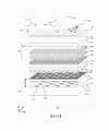
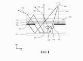
圖1A為以側視透視圖說明用於環境照射604中之可切換私密顯示器100的示意圖,該顯示器包含OLED發射式空間光調變器48、視差障壁700、輸出偏振器218及反射控制四分之一波長延遲器228、反射性偏振器302、可切換偏振控制延遲器300,以及配置於OLED發射式空間光調變器48之輸出側上的額外偏振器318;且圖1B為以正視圖說明圖1A之光學堆疊中的光學層之對準的示意圖。1A is a perspective view illustrating a schematic view in
OLED發射式空間光調變器48包含配置於底板基板212上之像素層214中的紅色發射像素220、綠色發射像素222以及藍色發射像素224之陣列。像素經配置以沿著輸出方向輸出光400。紅色發射像素220、綠色發射像素222、藍色發射像素224包含發光二極體,該等發光二極體為包含有機發光材料232之有機發光二極體。The OLED emission type
紅色發射像素220、綠色發射像素222、藍色發射像素224之間的區226包含控制電子器件且通常對OLED像素層214具反射性。The
視差障壁700包含孔隙702之陣列,其中在孔隙之間具有視差障壁光吸收區704。視差障壁700被配置成孔隙702之二維陣列,每一紅色發射像素220、綠色發射像素222、藍色發射像素224與各別孔隙對準。The
視差障壁700配置於間隔物層216上,該間隔物層沿著軸線199與像素層214間隔視差距離d,該軸線沿著像素層214之平面的法線。The
輸出偏振器218配置於OLED發射式空間光調變器48之輸出上,輸出偏振器218為具有電向量透射方向219之線性偏振器。具有光軸方向229之反射控制四分之一波長延遲器228配置於輸出偏振器218與OLED發射式空間光調變器48之間。反射控制四分之一波長延遲器228可由諸如聚碳酸酯之拉伸雙折射膜提供。有利地,可提供低成本反射控制四分之一波長延遲器228。The
在圖1A至圖1B之實施例中,視差障壁700配置於像素層214與反射控制四分之一波長延遲器228之間。在其他實施例(未示出)中,反射控制四分之一波長延遲器228可由形成於像素層214與視差障壁700之間的層提供。例如,此類反射控制四分之一波長延遲器228可包含固化之反應性液晶層。有利地,延遲器可具備等於或小於期望厚度d之厚度,如下文將進一步描述。In the embodiment of FIGS. 1A to 1B, the
額外偏振器318配置於輸出偏振器218之輸出側上,額外偏振器318為線性偏振器。可切換偏振控制延遲器300配置於輸出偏振器218與額外偏振器318之間。輸出偏振器218及額外偏振器318經配置以傳遞各別經線性偏振之偏振狀態。The
可切換偏振控制延遲器300包含被動延遲器330A、330B及可切換液晶延遲器301,該可切換液晶延遲器包含透明基板312、316及可切換液晶層314。電壓驅動器350可用於選擇操作模式,且可由控制器352控制。The switchable
關於圖9、圖17D、圖22A至圖22B以及圖23A描述說明性實施例,如下文將進一步詳細描述。Illustrative embodiments are described with respect to FIGS. 9, 17D, 22A-22B, and 23A, which will be described in further detail below.
圖1A之實施例進一步包含配置於輸出偏振器218與至少一個可切換偏振控制延遲器300之間的反射性偏振器302,反射性偏振器302為線性偏振器,其電向量透射方向303配置成傳遞與輸出偏振器218相同的經線性偏振之偏振狀態。The embodiment of FIG. 1A further includes a
可切換偏振控制延遲器300及反射性偏振器302之結構及操作進一步詳細描述於美國專利公開案第2019-0086706號、美國專利公開案第2019-0250458號、美國專利公開案第2018-0321553號、美國專利公開案第2020-0159055號以及WIPO公開案第WO 2018/208618號中,該等公開案皆以全文引用的方式併入本文中。本說明書中之偏振控制延遲器可由本文中描述之延遲器中之任一者替換。The structure and operation of the switchable
下文將參考圖10A至圖10D進一步描述可切換液晶延遲器之操作。在私密操作模式下,至少一個可切換偏振控制延遲器300能夠同時進行以下操作:不向由輸出偏振器218沿著軸線199傳遞之光的正交偏振分量引入淨相對相移,該軸線沿著至少一個可切換偏振控制延遲器300之平面的法線;及向由反射性偏振器302沿著軸線197傳遞之光的正交偏振分量引入相對相移,該軸線傾斜於至少一個可切換偏振控制延遲器300之平面的法線。在公共操作模式下,至少一個可切換偏振控制延遲器300能夠同時進行以下操作:不向由輸出偏振器218沿著軸線199傳遞之光的正交偏振分量引入淨相對相移,該軸線沿著至少一個可切換偏振控制延遲器300之平面的法線;及大體上不向由反射性偏振器302沿著軸線197傳遞之光的正交偏振分量引入相對相移,該軸線傾斜於至少一個可切換偏振控制延遲器300之平面的法線。Hereinafter, the operation of the switchable liquid crystal retarder will be further described with reference to FIGS. 10A to 10D. In the private mode of operation, at least one switchable
在與反射性偏振器302組合時,此輸出光相位控制有利地實現了在私密模式下降低圖1A之顯示器的離軸亮度並增大其離軸反射率。在公共模式下,在廣泛範圍之極角上實現了高透射率及低顯示反射率。此外,在兩操作模式下,對於同軸顯示器使用者而言,實現了高透射率及低反射率。有利地,顯示器使用者在兩模式下皆看到高亮度及高對比度影像,而離軸窺探者在私密模式下看到高視覺安全等級,且離軸使用者在公共模式下看到高影像可見性。When combined with the
現將描述視差障壁700之結構及操作。The structure and operation of the
在發射式顯示器中,通常在高極角下提供高亮度。諸如OLED顯示器之典型發射式顯示器可例如在60度之極角下提供大於正面亮度之25%的亮度。包含無機LED之微型LED顯示器可具有大體上朗伯亮度輸出,因此在60度下之亮度可能接近正面亮度之100%。In emissive displays, high brightness is usually provided at high polar angles. A typical emissive display such as an OLED display can provide a brightness greater than 25% of the front brightness at a polar angle of 60 degrees, for example. Micro LED displays containing inorganic LEDs can have substantially Lambertian brightness output, so the brightness at 60 degrees may be close to 100% of the front brightness.
如將在圖11A至圖11B中所描述,可切換偏振控制延遲器300通常配置成在設計之極座標位置處提供最佳視覺安全等級。此極座標位置可例如為+/-45度之側角及0度之仰角。在與設計之極座標位置存在5度不同之側角下,亮度之降低及反射率之增大被降低。As will be described in FIGS. 11A to 11B, the switchable
期望提供如下可切換私密顯示器:其在私密模式下在大於45度之極角下具有高視覺安全性,而在公共模式下在大於45度之極角下具有高影像可見性。為了在典型環境照明條件下實現高影像可見性,期望之離軸亮度可為正面亮度之至少2.5%,且較佳為至少5%。為了在典型環境照明條件下實現高影像安全性,期望之離軸亮度可小於1%,且較佳為小於0.5%。進一步期望在極座標視角情況下提供低色度變化。It is desirable to provide a switchable private display that has high visual security at a polar angle greater than 45 degrees in the private mode, and high image visibility at a polar angle greater than 45 degrees in the public mode. In order to achieve high image visibility under typical ambient lighting conditions, the desired off-axis brightness can be at least 2.5% of the front brightness, and preferably at least 5%. In order to achieve high image security under typical ambient lighting conditions, the desired off-axis brightness can be less than 1%, and preferably less than 0.5%. It is further desirable to provide low chromaticity changes in the case of polar coordinates viewing angle.
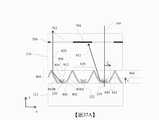
圖2A至圖2B為以側視圖說明用於圖1A至圖1B之可切換私密顯示器100的視差障壁700之示意圖。圖2A至圖2B說明在孔隙702最接近之方向θ上的橫截面。FIGS.2A-2B illustrate a side view of FIGS. 1A-1B may be switched disparity of
可假定未進一步詳細論述的圖2A至圖2B之配置的特徵對應於具有如上文所論述之等效附圖標記的特徵,包括特徵中之任何潛在變化。It can be assumed that the features of the configurations of Figures 2A-2B that are not discussed in further detail correspond to features with equivalent reference numerals as discussed above, including any potential variations in the features.
出於描述之目的,由單塊層110指示配置在視差障壁之輸出處的諸如偏振器及延遲器之各種輸出層。For the purpose of description, the
藉助於模擬延遲器堆疊、視差障壁、像素配置以及運用顯示器光學堆疊之實驗,已建立視差障壁之結構的期望範圍。With the aid of simulated retarder stacking, parallax barriers, pixel configuration, and experiments using display optical stacking, the desired range of the structure of the parallax barriers has been established.
沿著垂直於OLED發射式空間光調變器48之軸線199引導的同軸光線710被引導穿過寬度為a之各別對準孔隙702。孔隙大小a大於像素寬度w以實現正面方向之100%亮度。因此,沿著孔隙702最接近之方向,孔隙702之寬度a及紅色發射像素220、綠色發射像素222、藍色發射像素224之寬度w滿足如下要求:a
一些離軸光線726被引導至離軸方向,使得相比於同軸光線710之正面亮度,該離軸方向上之亮度降低。由視差障壁提供之最小吸收期望為50%,使得沿著孔隙702最接近之方向,孔隙702之寬度a,紅色發射像素220、綠色發射像素222、藍色發射像素224之間距p,以及紅色發射像素220、綠色發射像素222、藍色發射像素224之寬度w滿足如下要求:a
來自紅色發射像素220、綠色發射像素222、藍色發射像素224之一些光線712入射於視差障壁光吸收區704之下側上且可被吸收。當來自像素中心之光線712入射於視差障壁光吸收區704之中心上時,能提供最小透射角度。空氣中之極角
來自紅色發射像素220、綠色發射像素222、藍色發射像素224之中心的入射於視差障壁700吸收區之邊緣上的光線716的空氣中之極角為
在其他實施例中,期望角度

對於在像素最接近之方向上的50微米像素間距,及像素層214與視差障壁700之間的1.5之介質折射率,表1中以微米為單位給出了說明性尺寸。
因此,視差障壁間隔物層216之厚度d約為30 μm。此厚度為OLED面板之典型囊封層的典型厚度,如將在下文進一步描述。視差障壁700可形成為與像素層214具有期望之接近度,以有利地實現可切換私密顯示器之期望效能。Therefore, the thickness d of the parallax
藉助於與本實施例之比較,表2說明兩視圖視差障壁裸眼式立體顯示器對於相同像素間距及像素寬度之結構,其中像素列指向檢視窗,每一窗提供左眼或右眼影像。對於60mm之最小窗大小、67mm之最大窗大小、250mm之最小檢視距離以及700mm之最大窗距離,提供期望厚度範圍。
有利地,相比用於裸眼式立體顯示器之情況,本實施例實現增大之亮度及較低的厚度。裸眼式立體顯示器視差障壁無法實現期望的私密顯示器亮度控制特性。Advantageously, this embodiment achieves increased brightness and lower thickness compared to the case of a naked-eye stereoscopic display. The parallax barrier of the naked-eye stereoscopic display cannot achieve the desired brightness control characteristics of the private display.
一些光線714可以大於臨界角之角度穿過孔隙702,且因此被全內反射。此類光線可被視差障壁光吸收區704之頂部吸收。下文將進一步論述其他吸收機制。Some
視差障壁光吸收區704可為部分吸收的。由於吸收材料的吸收率降低,一些光線712可穿過視差障壁光吸收區704。另外或替代地,視差障壁光吸收區704可配置有子孔隙722,其配置成准許傳播光線712。子孔隙722可具有配置成在公共操作模式下提供期望的照射分佈之大小及密度。The parallax barrier
在說明性實例中,視差障壁光吸收區704可藉助於子孔隙722透射5%之入射光線。對於朗伯發射紅色像素220、綠色像素222、藍色像素224,在給定像素間距p及像素大小a的情況下,藉助於控制子孔隙722之密度及大小以及孔隙寬度,在60度之角度下的亮度可經配置為5%。在私密模式下,亮度可小於1%。有利地,在公共操作模式下可增大影像可見性,同時可藉助於可切換偏振控制延遲器300在私密模式下實現高視覺安全等級。In an illustrative example, the parallax barrier
現將描述視差障壁間距p'相比於像素間距p之配置。The configuration of the parallax barrier pitch p′ compared to the pixel pitch p will now be described.
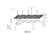
圖3A為以側視透視圖說明圖1A之視差障壁700與紅色發射像素220、綠色發射像素222、藍色發射像素224對於非瞳孔輸出之對準的示意圖。InFIG.3A is a side perspective view illustrating the
視差障壁700將來自每一紅色發射像素220、綠色發射像素222、藍色發射像素224之光引導至共同檢視窗26。在 圖3A中,共同檢視窗被傾斜對準,換言之,來自每一像素之共同子窗26與經對準障壁孔隙702在無限遠處重疊且被準直。窗表示來自每一縫隙之光的角度分佈。有利地,此配置跨越可切換私密顯示器100之區域提供與可切換偏振控制延遲器300及輸出偏振器218、額外偏振器318類似之空間衰減。對於移動的觀察者而言,實現了跨越顯示區域之自然影像均勻性變化,即最接近使用者之顯示器部分顯得最亮。The
圖3B為以側視透視圖說明圖1A之視差障壁700與紅色發射像素220、綠色發射像素222、藍色發射像素224對於瞳孔輸出之對準的示意圖。沿著孔隙702最接近之方向的間距p’小於沿著紅色發射像素220、綠色發射像素222、藍色發射像素224最接近之方向的各別對準紅色發射像素220、綠色發射像素222、藍色發射像素224之間距p。在任何給定方向上,最接近孔隙702之間距s'小於各別對準紅色發射像素220、綠色發射像素222、藍色發射像素224之間距s。InFIG3B is a side perspective view illustrating the
檢視窗26形成在處於OLED發射式空間光調變器48之輸出側上的距離v處的檢視窗平面處,使得檢視窗重疊之共同檢視窗處於有限距離處。有利地,對於位於窗平面處之正面觀察者而言,增大了跨越顯示器區域之亮度均勻性。The
視差障壁之孔隙中之至少一些可包含濾色器703R、703G、703B,因此視差障壁之孔隙包含紅色、綠色以及藍色濾色器之陣列。濾色器可對應於各別對準紅色發射像素220、綠色發射像素222、藍色發射像素224之色彩。濾色器降低了來自例如藍光洩漏至紅色發射像素孔隙之色彩串擾,從而有利地實現了色域增大。At least some of the apertures of the parallax barrier may include
替代地,僅孔隙702中的一些可包含濾色器,例如對應於紅色及綠色發射像素220、222之孔隙702可包含黃色透射濾色器。在一些實施例中,可藉由例如藍色發射像素及對準至紅色發射像素220、綠色發射像素222之色彩轉換材料來實現彩色發射,以實現彩色輸出。孔隙702之黃色濾色器可提供對殘餘藍光之吸收,從而有利地實現了色域增大。Alternatively, only some of the
孔隙702之濾色器的材料可包含非散射或低散射材料,使得維持了孔隙702及視差障壁光吸收區704之角度控制功能。The material of the color filter of the
可假定未進一步詳細論述的圖3A至圖3B之配置的特徵對應於具有如上文所論述之等效附圖標記的特徵,包括特徵中之任何潛在變化。It can be assumed that the features of the configurations of Figures 3A to 3B that are not discussed in further detail correspond to features with equivalent reference numerals as discussed above, including any potential variations in the features.
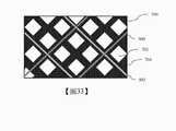
圖4為以俯視圖說明均勻發射紅色發射像素220、綠色發射像素222、藍色發射像素224及視點位置260、262、264對於各種極座標視角之配置的示意圖。FIG4 is a top plan view illustrating a uniform emission in a
紅色發射像素220、綠色發射像素222、藍色發射像素224以行及列的方式配置,孔隙702最接近之方向相對於輸出線性偏振器之電向量透射方向219成45度;且每一紅色發射像素220、綠色發射像素222、藍色發射像素224具有正方形形狀的發光區,其邊緣相對於輸出線性偏振器之電向量透射方向旋轉了45度。The
孔隙702具有正方形形狀,其邊緣相對於輸出線性偏振器之電向量透射方向旋轉了45度。The
視點位置260、262、264表示觀察者之瞳孔在由孔隙702提供之像素層214處的影像。視點位置260表示正面觀察者之瞳孔的位置。由於視點位置260具有大於像素之大小,因此觀察者看到與像素亮度相同之亮度且實現了100%之亮度。The viewpoint positions 260, 262, and 264 represent the image of the pupil of the observer at the
對於視點位置262,觀察者之眼睛位於顯示象限(具有非零側角及仰角)中,且處於最小透射率下。對於視點位置262,觀察者之眼睛定位成具有零仰角及側向偏移且處於最小透射率下。For the
視點位置264相比視點位置262與同軸位置具有較大間隔,使得最小透射率在象限中而非在側向方向上最接近。有利地,可最佳化檢視象限中之抑制作用。The
此外,圖4之像素配置實現了水平及豎直線之期望渲染,同時相比於綠色像素之數目,降低了紅色及藍色像素之數目。In addition, the pixel configuration of FIG. 4 realizes the desired rendering of horizontal and vertical lines, while reducing the number of red and blue pixels compared to the number of green pixels.
OLED顯示器通常為紅色、綠色以及藍色像素提供不同的發射區域,此係由於各別材料系統之不同發光率(發光度/mm2)。藉助於比較,在圖4之實施例中,本揭示案之紅色發射像素220、綠色發射像素222、藍色發射像素224在與二維孔隙702陣列一起使用時包含對於所有像素具有大體上相同區域之發射區。有利地,可最小化白點隨視角之變化。OLED displays usually provide different emission areas for red, green and blue pixels due to the different luminous rates (luminance/mm2 ) of the respective material systems. By comparison, in the embodiment of FIG. 4, the
期望補償OLED顯示器中之紅色、綠色以及藍色發射體的不同發光率,以實現期望之白點。It is desirable to compensate for the different luminous rates of the red, green, and blue emitters in the OLED display to achieve the desired white point.
每一紅色發射像素220、綠色發射像素222、藍色發射像素224之發光率可藉由調整不同的彩色像素之間的驅動電流來變化,使得能維持白點。因此,相比習知使用情況,綠色發射像素222可具有例如兩倍的發射區域。可降低用於綠色發射像素222及紅色發射像素220之驅動電流以實現期望之白點。The luminous efficiency of each
可能期望提供與用於典型OLED顯示器相同的驅動電流。It may be desirable to provide the same drive current as used for typical OLED displays.
圖5為以俯視圖說明結構化發射紅色發射像素220、綠色發射像素222、藍色發射像素224及視點位置對於各種極座標視角之配置的示意圖。FIG.5 is a schematic diagram illustrating the arrangement of the structured emission
對於紅色發射像素220、綠色發射像素222、藍色發射像素224中之至少一些,像素中之至少一些的發光區包含發光子區232R、232G、232B及非發光子區234。對於紅色發射像素220、綠色發射像素222以及藍色發射像素224,發光子區與非發光區的面積比不同。子區232R、232G、232B可對於像素中之每一者設置於相同區域內。子區232之分佈及視點位置260大小可經配置以提供亮度隨極角之大體上均勻衰減,以有利地最小化白點隨視角之變化;且可為紅色發射像素220、綠色發射像素222、藍色發射像素224中之每一者提供期望的驅動電流。For at least some of the
可假定未進一步詳細論述的圖4至圖5之配置的特徵對應於具有如上文所論述之等效附圖標記的特徵,包括特徵中之任何潛在變化。It can be assumed that the features of the configurations of Figures 4 to 5 that are not discussed in further detail correspond to features with equivalent reference numerals as discussed above, including any potential variations in the features.
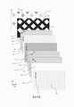
現將描述包含視差障壁700之OLED顯示器的結構。The structure of the OLED display including the
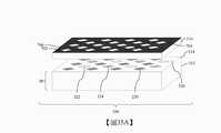
圖6為以側視圖說明OLED發射式空間光調變器48及包含上部進入減少層750、752之對準視差障壁700的結構之示意圖。FIG6 is a side view illustrate OLED emissive spatial light modulator comprising an
像素層214形成於底板基板212上且包含薄膜控制電路240,該薄膜控制電路包含薄膜電晶體、電容器、電極以及其他電子控制組件。電通孔242提供至通常具反射性之電極230的連接。發射層232R、232G、232B配置於電子傳遞層236R、232G、232B與電洞傳遞層238R、238G、238B之間。透明電極244配置成提供輸出側電連接。The
發射層厚度233R、233G、233B及電子傳遞層厚度237R、237G、237B可經調整以提供合適的光輸出特性。對於紅色發射像素220、綠色發射像素222、藍色發射像素224中的紅色、綠色以及藍色發光區中之每一者,發光材料之厚度233R、233G、233B係不同的。The thickness of the
在另一配置(未示出)中,電洞傳遞層238及電子傳遞層236可替代地配置於發射區232下方及上方。像素層214之總厚度通常可為一微米或更小,且因此相比於間隔物層216之距離,發射層232之位置差異較小。In another configuration (not shown), the
可切換私密顯示器100具有配置於像素層214與視差障壁700之間的間隔物層216中的一或多個額外層750、752,其中紅色發射像素220、綠色發射像素222、藍色發射像素224、一或多個額外層以及視差障壁700形成為單塊堆疊。一或多個額外層包含配置成提供對水及氧氣之障壁的至少一個透光無機層752。材料752可例如為諸如SiOx之氧化物材料。The
層750可具備有機材料。底板基板212可進一步具備層750、752(未示出)。在維持具有期望機械性能之可撓性顯示結構的同時,可抑制水及氧氣的進入。有利地,可增大顯示器壽命。The
總厚度d可經調整以有利地實現期望之亮度衰減,如本文中在別處所描述。The total thicknessd can be adjusted to advantageously achieve the desired brightness attenuation, as described elsewhere herein.
視差障壁700進一步包含配置成提供對水及氧氣之障壁的至少一個透光無機材料。有利地,可增大壽命。此外,可在視差障壁光吸收區704中提供非透射障壁層,以在至少部分障壁上增大進入抑制作用。The
可能期望進一步減少進入。視差障壁700配置於像素層214與配置成提供對水及氧氣之障壁的至少一個透光無機層752之間。無機層752被有機層750隔開。有利地,可在可撓性基板中提供對水及氧氣進入之高抗性。It may be desirable to further reduce entry. The
圖7為以側視圖說明OLED發射式空間光調變器48及包含玻璃材料110之對準視差障壁的結構之示意圖。相比於圖6之配置,可提供用於覆蓋層217之玻璃材料110,相比於圖6之層752、750,玻璃材料提供對氧氣及水進入之高障壁層抗性。間隔物層216可由黏著材料或聚合物材料提供。替代地,間隔物層216可由玻璃材料提供,在製造底板基板212及像素層214之後藉由化學機械拋光薄化該玻璃材料以實現期望厚度d。FIG.7 is a schematic diagram illustrating the structure of the OLED emission type
可假定未進一步詳細論述的圖6A至圖6B之配置的特徵對應於具有如上文所論述之等效附圖標記的特徵,包括特徵中之任何潛在變化。It can be assumed that the features of the configurations of Figures 6A-6B that are not discussed in further detail correspond to features with equivalent reference numerals as discussed above, including any potential variations in the features.
現將進一步詳細描述視差障壁700之透射率分佈的配置。The configuration of the transmittance distribution of the
圖8A至圖8C為說明各種視差障壁700結構之視差障壁700透射率隨位置變化之示意性曲線圖。8A to8C for explaining the structure of the
圖8A說明相對透射率相對於孔隙最接近之方向
圖8B說明例如藉由控制用於形成視差障壁光吸收區704之材料的厚度而增大視差障壁光吸收區704之透射率705。在孔隙702之間的視差障壁700區的吸收率小於100%,且大於80%,較佳地大於90%且更佳為大於95%。透射率705可例如小於5%或小於2.5%。有利地,在公共操作模式下可在較高極座標視角下提供增大之亮度。FIG. 8B illustrates that the
圖8C說明藉助於例如如圖2A中所說明之子孔隙區722而增大視差障壁光吸收區704之透射率。跨越視差障壁光吸收區704之平均透射率705可例如小於5%或小於2.5%。有利地,在公共操作模式下可在較高極座標視角下提供增大之亮度。FIG. 8C illustrates increasing the transmittance of the parallax barrier
現將描述圖1A之偏振延遲器的說明性實施例之結構。The structure of an illustrative embodiment of the polarization retarder of FIG. 1A will now be described.
可假定未進一步詳細論述的圖8A至圖8C之配置的特徵對應於具有如上文所論述之等效附圖標記的特徵,包括特徵中之任何潛在變化。It can be assumed that the features of the configurations of FIGS. 8A to 8C that are not discussed in further detail correspond to features with equivalent reference numerals as discussed above, including any potential variations in the features.
在圖1A至圖1B之實施例中,可切換偏振控制延遲器300包含被動偏振控制延遲器330及可切換液晶延遲器301,但大體上可由至少一個延遲器之其他組態替換,下文所描述的裝置中存在該等組態之一些實例。In the embodiment of FIGS. 1A to 1B, the switchable
圖9為以透視側視圖說明可切換偏振控制延遲器300之配置的圖式,該可切換偏振控制延遲器包含:包含具有均勻對準之可切換液晶層314的可切換液晶延遲器301,及交叉之A板偏振控制延遲器330A、330B。可假定未進一步詳細論述的圖9之配置的特徵對應於具有如上文所論述之等效附圖標記的特徵,包括特徵中之任何潛在變化。9 is a perspective side view illustrating the switchable polarization control figures arranged
表3中給出說明性實施例及私密與公共模式下之極座標分佈。
可切換液晶延遲器301包含兩個表面對準層419a、419b,該兩表面對準層鄰近於液晶材料421的層安置且在液晶材料層之相對側上,且每一對準層配置成在鄰近液晶材料421中提供均勻對準。可切換液晶延遲器301之液晶材料421的可切換液晶層314包含具有正介電各向異性之液晶材料421。The switchable
被動偏振控制延遲器330由具有交叉軸線之一對A板330A、330B提供。在本實施例中,「交叉」指兩個延遲器在延遲器之平面中的光軸之間的大體上90º之角度。為了降低延遲器材料之成本,期望提供例如由於膜製造期間之拉伸錯誤而使延遲器定向具有一定變化之材料。延遲器定向遠離較佳方向之變化可降低正面亮度且增大最小透射率。較佳地,角度310A至少為35º且至多為55º,更佳為至少40º且至多為50º,且最佳為至少42.5º且至多為47.5º。較佳地,角度310B至少為125º且至多為145º,更佳為至少130º且至多為135º,且最佳為至少132.5º且至多為137.5º。The passive
均勻對準有利地降低機械變形期間,諸如在觸碰顯示器時的恢復時間。可使用拉伸膜提供被動延遲器330A、330B,以有利地實現低成本及高均勻性。此外,具有均勻對準之液晶延遲器的視場得到增大,同時在施加壓力期間能彈性提供液晶材料流動之可見性。Uniform alignment advantageously reduces the recovery time during mechanical deformation, such as when touching the display. A stretched film can be used to provide the
在可切換液晶延遲器301之第一可切換狀態中,至少一個可切換偏振控制延遲器300配置成同時進行以下操作:不向由反射性偏振器302沿著軸線199傳遞之光的正交偏振分量引入淨相對相移,該軸線沿著至少一個可切換偏振控制延遲器300之平面的法線;及向由反射性偏振器302沿著軸線197傳遞之光的正交偏振分量引入淨相對相移,該軸線傾斜於至少一個可切換偏振控制延遲器300之平面的法線;並在可切換液晶延遲器301之第二可切換狀態中,同時進行以下操作:不向由反射性偏振器302沿著軸線199傳遞之光的正交偏振分量引入淨相對相移,該軸線沿著至少一個可切換偏振控制延遲器300之平面的法線;及不向由反射性偏振器302沿著軸線197傳遞之光的正交偏振分量引入淨相對相移,該軸線傾斜於至少一個可切換偏振控制延遲器300之平面的法線。In the first switchable state of the switchable
此類相移提供實現如下效果之偏振透射率及反射率分佈:(i)高同軸透射率及低反射率;(ii)在私密模式下,離軸透射率降低且反射率增大;以及(ii)在公共模式下,高離軸透射率及低反射率。有利地,可切換私密顯示器向正面使用者提供高影像品質,向離軸窺探者提供高視覺安全等級,且向離軸顯示器使用者提供高影像可見性,如現將描述。This type of phase shift provides polarization transmittance and reflectance distributions that achieve the following effects: (i) high on-axis transmittance and low reflectance; (ii) in private mode, off-axis transmittance decreases and reflectivity increases; and ( ii) In public mode, high off-axis transmittance and low reflectance. Advantageously, the switchable private display provides high image quality to frontal users, provides high visual security levels to off-axis pryers, and provides high image visibility to off-axis display users, as will now be described.
圖10A為以側視圖說明公共操作模式下輸出光自OLED發射式空間光調變器48傳播通過圖1A之光學堆疊的示意圖。FIG.10A is a schematic side view illustrating the output light propagating from the OLED emitting spatial
在公共操作模式下,由紅色發射像素220、綠色發射像素222、藍色發射像素224發射且在同軸方向上透射通過障壁700之孔隙702的同軸光線710具有平行於輸出偏振器218之電向量透射方向219之線性偏振狀態360。接著,同軸光線710穿過包含可切換液晶延遲器301及被動延遲器330之多個可切換偏振控制延遲器300。在公共模式下,可切換液晶延遲器301處於斷開狀態,其中跨越可切換液晶層314具有不同控制電壓。In the common operation mode, the
因此,當穿過可切換液晶延遲器301時,同軸光線710之偏振狀態經歷延遲。在被動延遲器330為C板延遲器之情況下,同軸光線710在大體上平行於被動延遲器330之光軸的方向上傳播。因此,當穿過被動延遲器330時,同軸光線710經歷最小延遲。離開複數個可切換偏振控制延遲器300之組合效果導致同軸光線710以相同或類似於同軸光線710進入複數個可切換偏振控制延遲器300之線性偏振狀態360的線性偏振狀態362離開複數個可切換偏振控制延遲器300。此線性偏振狀態362平行於額外偏振器318之電向量透射方向319,且因此同軸光線710以相對未經修改之亮度離開可切換私密顯示器100。Therefore, when passing through the switchable
在公共模式下,由障壁700之孔隙702透射之離軸光線726以類似於同軸光線710之方式穿過複數個可切換偏振控制延遲器300。因此,當可切換液晶延遲器301處於該兩個狀態中之第一狀態時,複數個可切換偏振控制延遲器300不會整體變換垂直於可切換延遲器之平面穿過的同軸光線710之線性偏振狀態360,或與垂直於可切換延遲器301之平面成銳角地穿過之離軸光線726的偏振狀態361。In the common mode, the off-
線性偏振狀態362與線性偏振狀態360大體上相同,且偏振狀態364與偏振狀態361大體上相同。因此,角度透射分佈大體上跨越寬極座標區一致地透射。The
換言之,當液晶材料414之可切換液晶層314處於該兩個狀態中之第一狀態時,複數個可切換偏振控制延遲器300不會整體延遲垂直於延遲器之平面穿過之光或與垂直於複數個可切換偏振控制延遲器300之平面成銳角地穿過之光。In other words, when the switchable
有利地,在第一狀態下,顯示亮度隨視角之變化大體上未經修改。多個使用者可自廣泛範圍之視角便利地檢視顯示器。Advantageously, in the first state, the change in display brightness with viewing angle is substantially unmodified. Multiple users can conveniently view the display from a wide range of viewing angles.
圖10B為以側視圖說明公共操作模式下光線自環境光源604傳播通過圖1A之光學堆疊的示意圖。FIG.10B is a schematic diagram illustrating the propagation of light from the ambient
環境光604之同軸光線410以類似於上文所論述的自紅色發射像素220、綠色發射像素222、藍色發射像素224發射之同軸光線710的方式穿過複數個可切換偏振控制延遲器300。儘管同軸光線410以與自紅色發射像素220、綠色發射像素222、藍色發射像素224發射之同軸光線710反向的方向穿過複數個可切換偏振控制延遲器300,但以反向方向穿過複數個可切換偏振控制延遲器300可並不改變如上文針對自紅色發射像素220、綠色發射像素222、藍色發射像素224發射之光所論述的複數個可切換偏振控制延遲器300對光線之影響。因此,同軸光線410到達視差障壁700之視差障壁光吸收區704,在吸收區上光線被吸收;或到達像素層214,在像素層上光線可被吸收或反射,如下文將進一步描述。The
以類似方式,離軸光線412在穿過複數個可切換偏振控制延遲器300時未經歷偏振狀態之整體變換。環境光604係非偏振的且離軸光線最初無偏振370。額外偏振器318傳遞平行於額外偏振器之電向量透射方向319的偏振分量372。額外偏振器318吸收垂直於額外偏振器318之電向量透射方向319的大部分偏振狀態372。一些光藉由外部空氣界面處的菲涅爾反射自額外偏振器318之前表面反射開。在穿過複數個可切換偏振控制延遲器300之後,離軸光線412之線性偏振狀態374因此平行於反射性偏振器302之電向量透射方向303,且離軸光線未被反射而是替代地穿過反射性偏振器302到達視差障壁700,在此處光線可被視差障壁吸收區吸收或透射至像素層214。反射光線412中的一些將進一步由視差障壁700之視差障壁光吸收區704吸收,如下文進一步描述。In a similar manner, the off-
有利地,在公共模式下,降低了跨越廣泛範圍之視角的顯示器反射率。多個使用者可便利地自廣泛範圍之視角以高影像對比度檢視顯示器。Advantageously, in the public mode, the reflectance of the display across a wide range of viewing angles is reduced. Multiple users can conveniently view the display with high image contrast from a wide range of viewing angles.
圖10C為以側視圖說明私密操作模式下輸出光自OLED發射式空間光調變器48傳播通過圖1A之光學堆疊的示意圖。FIG.10C is a schematic side view illustrating the output light propagating from the OLED emitting spatial
在私密模式下,可切換液晶延遲器301處於電壓被施加至可切換液晶層314之接通狀態。可切換液晶延遲器301可因此處於該兩個狀態中之第二狀態。在可切換液晶延遲器301具有正介電各向異性之情況下,可切換液晶延遲器301因此以類似方式在第二狀態下起作用,以調整輸出之入射偏振狀態之相位。同軸光線710在穿過處於第二狀態之可切換液晶延遲器301時未經歷延遲,且因此同軸光線710在穿過複數個可切換偏振控制延遲器300之前的線性偏振狀態360相同於在穿過複數個可切換偏振控制延遲器300之後的線性偏振狀態362。因此,在私密操作模式下,同軸光線710經由額外偏振器318以很大程度上不變之亮度離開顯示器。In the privacy mode, the switchable
在穿過可切換液晶延遲器301之材料時,自紅色發射像素220、綠色發射像素222、藍色發射像素224發射且透射通過障壁700之孔隙702的離軸光線726經歷偏振變換。此係由於離軸光線726以銳角進入該材料。因此,離軸光線726以線性偏振狀態364到達額外偏振器318處,該狀態在相比於線性偏振狀態361時至少部分地經旋轉。線性偏振狀態364具有與額外偏振器318之電向量透射方向319垂直之至少某一分量,且因此相比於同軸光線710,離軸光線726之亮度降低。When passing through the material of the switchable
有利地,在第二狀態下,可降低寬視角下之顯示亮度。因此,可防止窺探者在寬視角下檢視由可切換私密顯示器100發射之影像。在夜間操作時可降低雜散光,而正面使用者可看到影像。Advantageously, in the second state, the display brightness under a wide viewing angle can be reduced. Therefore, it is possible to prevent snoopers from viewing the images emitted by the switchable
圖10D為以側視圖說明私密操作模式下光線自環境光源604傳播通過圖1A之光學堆疊的示意圖。10Dis a schematic side view illustrating the propagation of light from the ambient
在私密模式操作下,來自環境光源604之入射同軸光線410以類似於如關於圖10C所描述的自紅色發射像素220、綠色發射像素222、藍色發射像素224發射之同軸光線710的方式穿過複數個可切換偏振控制延遲器300。儘管同軸光線410以與自紅色發射像素220、綠色發射像素222、藍色發射像素224發射之同軸光線710反向的方向穿過複數個可切換偏振控制延遲器300,但穿過複數個可切換偏振控制延遲器300進入顯示器或離開顯示器之方向可並不改變如針對自紅色發射像素220、綠色發射像素222、藍色發射像素224發射之光所論述的複數個可切換偏振控制延遲器300對光線之影響。因此,同軸光線410到達視差障壁700,在此處光線可被視差障壁吸收區吸收或透射至像素層214。反射光線412中的一些將進一步由視差障壁700之視差障壁光吸收區704吸收,如下文進一步描述。In private mode operation, the incident coaxial light 410 from the ambient
與此對比,離軸光線412在穿過可切換液晶延遲器301之液晶材料414時會經歷偏振變換。此係由於離軸光線412以銳角進入該材料,如下文進一步詳細論述。因此,離軸光線412以線性偏振狀態374到達反射性偏振器302處,該狀態在相比於線性偏振狀態372時至少部分地經旋轉。線性偏振狀態374具有與反射性偏振器302之電向量透射方向303垂直之至少某一狀態,且因此至少部分地由反射性偏振器302反射。光線412接著以反向方向穿過複數個可切換偏振控制延遲器300,從而使來自第一次穿過複數個可切換偏振控制延遲器300的偏振轉換反向並產生平行於額外偏振器318之電向量透射方向的偏振狀態376。因此,離軸光線412以偏振狀態378離開可切換私密顯示器100,從而導致在自廣角檢視時該堆疊看起來像反射鏡。額外偏振器318吸收垂直於額外偏振器之電向量透射方向319的大部分偏振狀態372,但可反射一小部分垂直狀態404。In contrast, the off-
有利地,在第二狀態下,可增大寬視角下之反射率。因此,由於反射光降低了由顯示裝置發射之影像的對比度,可防止窺探者在寬視角下檢視由可切換私密顯示器100發射之影像,且因此由於反射率R增大而增大了如上文等式7中所描述之視覺安全等級VSL。Advantageously, in the second state, the reflectivity under a wide viewing angle can be increased. Therefore, because the reflected light reduces the contrast of the image emitted by the display device, it can prevent prying eyes from viewing the image emitted by the switchable
可假定未進一步詳細論述的圖10A至圖10D之配置的特徵對應於具有如上文所論述之等效附圖標記的特徵,包括特徵中之任何潛在變化。It may be assumed that the features of the configurations of FIGS. 10A to 10D that are not discussed in further detail correspond to features with equivalent reference numerals as discussed above, including any potential variations in the features.
現將描述說明性實施例之模擬輸出。The analog output of the illustrative embodiment will now be described.
圖11A為圖1A之配置的組件貢獻及輸出之極座標圖陣列,其包含OLED發射式空間光調變器48亮度、視差障壁700透射率、可切換偏振控制延遲器300透射率、經歸一化可切換偏振控制延遲器300反射性、公共模式亮度、私密模式亮度以及對於1.0之勒克斯/尼特比的視覺安全等級之極座標圖;且圖11B為圖11A之配置的組件貢獻及輸出之線性分佈圖陣列,其包含在0度(東方向)、90度(北方向)、45度(東北方向)以及225度(西南方向)的方位角下的線性分佈。出於當前描述之目的,在圖11A之SLM亮度圖上說明圖11B中之分佈的方位定向。FIG.11A is a polar coordinate map array of the component contribution and output of the configuration of FIG. 1A, which includes the OLED emission spatial
在表4之第一列中參考在像素最接近方向上之50 μm間距p提供圖11A至圖11B之說明性視差障壁700及OLED像素的參數。以圖4之菱形配置提供紅色發射像素220、綠色發射像素222、藍色發射像素224。像素最接近之方向為45度之方位角。
在考慮額外偏振器318透射率及反射性偏振器302對偏振光之反射率之後,使用36%的峰值eQM反射率,其對應於經歸一化可切換延遲器反射性圖上的100%輪廓。After considering the transmittance of the
SLM 48亮度圖說明OLED顯示器提供非朗伯亮度衰減,其中通常在50度之極角下提供大於20%之正面亮度。The
視差障壁700透射率圖說明由於此定向中的像素之不同間隔而引起的0度與45度方位角之分佈差異。The transmittance diagram of the
可切換偏振控制延遲器300透射率及反射率圖說明使用圖9之結構沿著側向方向控制相位。The transmittance and reflectance diagrams of the switchable
藉由視差障壁700對來自OLED發射式空間光調變器48之光的透射來判定公共模式照度。可切換偏振控制延遲器300僅提供此亮度分佈之較小調變。The common mode illuminance is determined by the transmission of the light from the OLED emitting spatial
私密模式亮度說明在側向方向上及上部檢視象限中提供小於1%之亮度。顯示器對於0度側角及繞水平軸旋轉具有高可見性。有利地,可設定舒適視角以由使用者自同軸位置檢視顯示器。The privacy mode brightness description provides less than 1% brightness in the lateral direction and in the upper viewing quadrant. The display has high visibility for 0 degree side angle and rotation around the horizontal axis. Advantageously, a comfortable viewing angle can be set to allow the user to view the display from a coaxial position.
現將描述環境光位準對視覺安全等級之影響。The impact of ambient light level on the level of visual safety will now be described.
圖11C為圖11A至圖11B之說明性實施例在0.25之勒克斯/尼特比的情況下之極座標分佈圖及線性極座標分佈圖。表4之第二列中描述可切換私密顯示器100之性質。FIG11C polar and linear profile polar profile of the embodiment in the case of 0.25 lux / nits ratio illustrative embodiment of FIGS. 11A to 11B of FIG. The second column of Table 4 describes the properties of the switchable
視覺安全等級(VSL)圖係取決於環境照度條件。環境照度提供為正面亮度之比率。因此,在典型的辦公環境中,具有300尼特之正面亮度的顯示器與落在顯示器上的300勒克斯環境照度具有1.0之勒克斯/尼特比。在較暗的飛機艙中,對於25尼特的環境照度可提供100尼特之正面亮度,從而提供0.25之勒克斯/尼特比。The visual safety level (VSL) diagram depends on the environmental illuminance conditions. The ambient illuminance is provided as the ratio of frontal brightness. Therefore, in a typical office environment, a display with a front brightness of 300 nits and an ambient illuminance of 300 lux falling on the display have a ratio of 1.0 lux/nit. In a darker cabin, it can provide a frontal brightness of 100 nits for an ambient illuminance of 25 nits, thereby providing a lux/nit ratio of 0.25.
本實施例之可切換反射率在低勒克斯/尼特比下增大了視覺安全等級。此外,視差障壁700可進一步降低離軸亮度,以有利地在低照度條件下進一步增大視覺安全性。The switchable reflectance of this embodiment increases the visual safety level at a low lux/nit ratio. In addition, the
藉助於實驗及模擬已判定,對於所顯示影像與離軸窺探者之高度隔離,期望在私密模式下的視覺安全等級大於3.0且較佳地大於4.0。亦藉助於實驗及模擬判定,大於50%且較佳地大於83.3%之影像可見性W(公共模式下的視覺安全等級V小於2.0且較佳地小於1.2)實現了所顯示影像至離軸使用者之期望影像可見性。With the aid of experiments and simulations, it has been determined that for the high isolation between the displayed image and off-axis prying eyes, it is expected that the visual security level in the private mode is greater than 3.0 and preferably greater than 4.0. Also with the aid of experiments and simulations, an image visibility W greater than 50% and preferably greater than 83.3% (the visual safety level V in public mode is less than 2.0 and preferably less than 1.2) realizes the off-axis use of the displayed image The viewer expects image visibility.
圖11B至圖11C之視覺安全等級線性分佈說明,在至少45度之側角下及對於側向方向上的方位角,以及小於0.25勒克斯/尼特之照射條件下的檢視象限中,可對於側角及檢視象限實現大於4.0之視覺安全等級。有利地,可在廣泛範圍之極座標位置上針對離軸使用者實現高視覺安全等級。視覺安全等級在側向方向上的較高極角下並不降級。The linear distribution of visual safety levels in Fig. 11B to Fig. 11C shows that under the side angle of at least 45 degrees and for the azimuth angle in the lateral direction, and the viewing quadrant under the illumination condition of less than 0.25 Lux/nit, it can be used for the side The angle and viewing quadrant achieve a visual safety level greater than 4.0. Advantageously, a high level of visual safety can be achieved for off-axis users in a wide range of polar coordinate positions. The visual safety level does not degrade at higher polar angles in the lateral direction.
藉助於與本實施例之比較,現將描述省略視差障壁700的圖1A之配置的模擬外觀。By means of comparison with the present embodiment, the simulated appearance of the configuration of FIG. 1A in which the
圖12A為圖1A之配置對於移除視差障壁700之說明性配置的組件貢獻及輸出之極座標圖陣列,其包含OLED發射式空間光調變器48亮度、視差障壁700透射率、可切換延遲器透射率、可切換延遲器反射性、公共模式亮度、私密模式亮度以及1.0之勒克斯/尼特下的視覺安全等級之極座標圖;且圖12B為圖12A之配置的組件貢獻及輸出之線性分佈圖陣列,其包含在0、90、45以及225度之方位角下的線性分佈。表4之第三列中描述可切換私密顯示器100之性質。12A is a configuration diagram ofFIG. 1A for removal of the
藉助於與如將在圖12A至圖12B中描述之本實施例的比較,可切換偏振控制延遲器300可能無法在具有高離軸亮度位準之顯示器中實現期望的視覺安全等級,該亮度位準通常由不存在視差障壁700時之OLED發射式空間光調變器48提供。By means of a comparison with the present embodiment as will be described in FIGS. 12A to 12B, the switchable
在考慮側向(0度)方向上大於60度之角度下的視覺安全等級之線性極座標分佈圖時,對於1.0之勒克斯/尼特,VSL降為低於4.0。儘管在約45度之角度下具有高VSL,此配置仍向離軸窺探者提供不當的視覺安全性。When considering the linear polar coordinate distribution diagram of the visual safety level at an angle greater than 60 degrees in the lateral (0 degree) direction, for a lux/nit of 1.0, the VSL is reduced to less than 4.0. Despite having a high VSL at an angle of about 45 degrees, this configuration still provides improper visual safety to off-axis snoopers.
藉助於與本實施例之比較,現將描述省略可切換偏振控制延遲器300的圖1A之配置的模擬外觀。By way of comparison with the present embodiment, the simulated appearance of the configuration of FIG. 1A in which the switchable
圖13A為圖1A之配置對於移除可切換延遲器之說明性配置的組件貢獻及輸出之極座標圖陣列,其包含OLED發射式空間光調變器48亮度、視差障壁700透射率、可切換延遲器透射率、可切換延遲器反射性、公共模式亮度、私密模式亮度以及對於1.0之勒克斯/尼特的視覺安全等級之極座標圖;且圖13B為圖13A之配置的組件貢獻及輸出之線性分佈圖陣列,其包含在0、90、45以及225度之方位角下的線性分佈。FIG.13A is a polar coordinate map array of the component contribution and output of the illustrative configuration of the configuration of FIG. 1A for removing the switchable retarder, which includes the OLED emission spatial
表4之第四列中描述可切換私密顯示器100之性質。視差障壁厚度700被設計成最小厚度,以對於側向方向上之45度極角在至少一個方位角下提供大於4.0之VSL。The fourth column of Table 4 describes the properties of the switchable
此顯示器在廣泛範圍之極座標視角,且尤其在大體上未降低孔隙大小且後續存在不當的透射效率損耗之檢視象限上具有不當的私密效能。This display has improper privacy performance in a wide range of polar coordinate viewing angles, and especially in the inspection quadrant where the pore size is not substantially reduced and the subsequent improper transmission efficiency loss occurs.
現將進一步考慮在公共操作模式下環境光自圖1A之可切換私密顯示器100的表面之光譜透射及光譜反射。The spectral transmission and spectral reflection of ambient light from the surface of the switchable
圖14為以側視圖說明圖1A之可切換私密顯示器100中的環境光之反射的示意圖。可假定未進一步詳細論述的圖14之配置的特徵對應於具有如上文所論述之等效附圖標記的特徵,包括特徵中之任何潛在變化。FIG.14 is a schematic diagram illustrating the reflection of ambient light in the
同軸光線710由線性輸出偏振器218、額外偏振器318傳遞,其中輸出偏振器218、額外偏振器318之光譜透射率提供對來自紅色發射像素220、綠色發射像素222、藍色發射像素224之光的光譜修改。The
光線714、715自可切換私密顯示器100之外表面向內反射。入射時被吸收的光線714被引導至視差障壁700視差障壁光吸收區704上。光線715自反射性像素層214反射開。反射減少四分之一波長延遲器228提供在反射時經歷相變之圓形偏振狀態442,以在反射之後提供圓形偏振狀態444,該圓形偏振狀態被轉換成與電向量透射方向219正交且被吸收之偏振狀態。The light rays 714 and 715 are reflected inwardly from the outer surface of the
因此,光線714、715兩次或三次穿過輸出偏振器218、額外偏振器318,從而相應地修改光譜吸收。Therefore, light 714, 715 passes through the
視差障壁700配置成吸收入射於其上的光。來自環境源604之光線410由輸出偏振器218、額外偏振器318傳遞且由視差障壁光吸收區704吸收。穿過障壁且被反射之光線412可在反射之後由障壁吸收。可切換私密顯示裝置100用於環境照射604中,且視差障壁700吸收自像素層214反射開的透射通過孔隙702之環境照射604光線412中之至少一些。The
將期望增大圖1A之可切換私密顯示器100的光譜透射率。此外,將期望增大藍色透射率而不降級顯示器反射之外觀。It would be desirable to increase the spectral transmittance of the
圖15為說明對於額外偏振器318為寬頻帶吸收式偏振器之情況,且對於額外偏振器318為洩漏吸收式偏振器之情況,輸出亮度隨波長變化的示意性曲線圖。分佈870說明平行的寬頻帶偏振器之透射亮度的變化;分佈872說明平行的洩漏偏振器之透射亮度的變化;分佈874說明交叉之寬頻帶偏振器的透射亮度之變化;且分佈876說明交叉之洩漏偏振器之透射亮度的變化。洩漏額外偏振器318在藍色光譜帶中具有增大之洩漏且透射率增大。FIG15 is a diagram for
輸出偏振器218及額外偏振器318在與相同材料之第二假想偏振器交叉時在自520nm至560nm之波長下的透射率小於在自450nm至490nm之波長下的透射率。在自450nm至490nm之波長下,透射率大於1%,較佳為大於2%且最佳為大於3%;且在自520nm至560nm之波長下,透射率小於3%,較佳為小於2%且最佳為小於1%。The transmittance of the
現將描述圖1A之可切換私密顯示器100在使用洩漏偏振器時的操作。The operation of the
圖16A為說明寬頻帶吸收式偏振器及洩漏吸收式偏振器之輸出偏振器218、額外偏振器318透射率隨波長,且相對於圖14之透射同軸光線710的紅色發射像素220、綠色發射像素222以及藍色發射像素224之光譜輸出890R、890G、890B的變化之示意性曲線圖。FIG16A is a diagram broadband absorptive polarizer and the polarizer leakage output of the
分佈882說明包含洩漏輸出偏振器218、額外偏振器318的圖1A之實施例的光譜透射率。
藉助於與本實施例之比較,分佈880說明包含寬頻帶吸收式輸出偏振器218、額外偏振器318的圖1A之實施例的光譜透射率。有利地,相比於包含寬頻帶輸出偏振器218、額外偏振器318之配置,由分佈882說明之本實施例在紅色、綠色以及藍色通道中實現了大體上較高透射率。By comparison with this embodiment, the
藉助於與本實施例之進一步比較,分佈870說明包含寬頻帶吸收式偏振器及寬頻帶反射率控制四分之一波長延遲器,且不包含視差障壁700、可切換偏振控制延遲器300或額外偏振器318之顯示器的光譜輸出。有利地,由分佈882說明之本實施例具有與不包含額外偏振器318之顯示器大體上相同的藍光透射率。高效之藍光發射增大OLED顯示器之壽命。有利地,本實施例實現了與並無額外偏振器318之習知顯示器相同的顯示器壽命。By means of further comparison with this embodiment, the
圖16B為說明寬頻帶吸收式輸出偏振器218、額外偏振器318及洩漏吸收式輸出偏振器218、額外偏振器318之反射率隨波長,且相對於圖14之反射光線的紅色發射像素220、綠色發射像素222以及藍色發射像素224之光譜輸出890R、890G、890B的變化之示意性曲線圖。FIG16B is a diagram output
至少部分藉由圖14中之光線440在反射減少四分之一波長延遲器228之後通過輸出偏振器218、額外偏振器318之透射率及視差障壁700之吸收率來判定反射率。The reflectance is determined at least in part by the light 440 in FIG. 14 passing through the
為了繼續表4之第一列的說明性實施例,視差障壁之孔徑比為25%,使得對於圖14之光線410、412,障壁吸收率為75%。返回至包含洩漏輸出偏振器218、額外偏振器318的圖14之實施例,分佈888說明在視角上積分的顯示器之平均光譜透射率。有利地,可由顯示器提供極低平均反射率。此外,如圖16A中所說明,增大了顯示器效率。To continue the illustrative embodiment in the first column of Table 4, the aperture ratio of the parallax barrier is 25%, so that for the
分佈884說明圖14之顯示器對於由視差障壁700之孔隙702透射且反射之光線440的光譜透射率。相比於分佈876,分佈884具有顯著經改良之吸光度,其中在峰值藍色光譜波長處之洩漏小於1%。有利地,實現了低反射率。The
藉助於與本實施例之進一步比較,分佈886說明包含寬頻帶吸收式偏振器及寬頻帶反射率控制四分之一波長延遲器,且不包含視差障壁700、可切換偏振控制延遲器300或額外偏振器318之顯示器的光譜輸出。此顯示器在寬光譜範圍上實現了低反射率且具有降低的光譜透射率。By means of further comparison with this embodiment, the
藉助於與本實施例之進一步比較,分佈876說明包含洩漏吸收式偏振器及寬頻帶反射率控制四分之一波長延遲器,且不包含視差障壁700、可切換偏振控制延遲器300或額外偏振器318之顯示器的光譜輸出。此顯示器在寬光譜範圍上實現了低反射率。此顯示器提供不當的光反射率,尤其在光譜之藍色及綠色部分中。具有光譜透射率分佈872、876之洩漏偏振器因此不適於發射式顯示器中的反射率控制。By means of further comparison with this embodiment, the
現將描述包含無機微型LED之實施例的操作。The operation of the embodiment including the inorganic micro LED will now be described.
圖17A為以側視透視圖說明用於環境照射604中之可切換私密顯示器100的示意圖,該顯示器包含微型LED發射式空間光調變器48、視差障壁700、輸出偏振器218及反射控制四分之一波長延遲器228、被動偏振控制延遲器380、反射性偏振器302、可切換偏振控制延遲器300以及配置於OLED發射式空間光調變器48之輸出側上的額外偏振器318;且圖17B為以正視圖說明圖17A之光學堆疊中的光學層之對準的示意圖。可假定未進一步詳細論述的圖18A至圖18B之配置的特徵對應於具有如上文所論述之等效附圖標記的特徵,包括特徵中之任何潛在變化。FIG17A is a schematic view of a display to be switchable privacy side perspective view illustrating the environment for the irradiation of 604 to 100, the LED display comprises a micro-emissive spatial
相比於OLED材料,包含無機微型LED之紅色發射像素220、綠色發射像素222、藍色發射像素224可具有超過103的發光率(lm/mm2)。為實現相同的亮度,微型LED紅色發射像素220、綠色發射像素222、224之區域可顯著小於用於OLED紅色發射像素220、綠色發射像素222、藍色發射像素224之區域。此外,由於降低了使用的單塊半導體區域,較小微型LED紅色發射像素220、綠色發射像素222、藍色發射像素224的成本較低。例如,對於在像素最接近之方向上具有50微米像素間距的情況,微型LED可具有小於5微米之寬度或直徑。Compared with OLED materials, the
期望實現在寬極座標範圍上具有高影像可見性之公共操作模式及對離軸窺探者具有高視覺安全等級的私密模式。It is desired to realize a public operation mode with high image visibility over a wide polar coordinate range and a private mode with a high visual security level for off-axis snoopers.
相比於圖1A之OLED像素層214的典型反射性像素層,像素層214可包含光吸收材料227以有利地實現反射率降低。Compared with the typical reflective pixel layer of the
圖17A不同於圖1A之處還在於包含具有圓形形狀之孔隙702。有利地,可增大透射率分佈對稱性。FIG. 17A is different from FIG. 1A in that it also includes an
紅色發射像素220、綠色發射像素222、藍色發射像素224配置於正方形網格而非菱形網格上。此配置降低了側向方向上的亮度且增大了象限中的亮度。有利地,在較小仰角下,可增大私密模式下的視覺安全等級,如下文將說明。The
在實施例(未示出)中,可提供包含OLED與微型LED像素之混合物的顯示器(未示出)。例如,可提供藍色微型LED及綠色與藍色OLED像素。有利地,可增大藍色壽命且並不使用微型LED之色彩轉換。In an embodiment (not shown), a display (not shown) containing a mixture of OLED and micro LED pixels may be provided. For example, blue micro LEDs and green and blue OLED pixels can be provided. Advantageously, the blue life can be increased without using micro-LED color conversion.
圖17C為以俯視圖說明微型LED發射紅色發射像素220、綠色發射像素222、藍色發射像素224及視點位置對於各種極座標視角之配置的示意圖。FIG.17C is a schematic diagram illustrating the arrangement of the micro LED emitting
圖17D為以側視透視圖說明配置於輸出偏振器218與反射性偏振器302之間的被動偏振控制延遲器380之示意圖。FIG.17D is a schematic diagram illustrating the passive
被動偏振控制延遲器380配置於輸出偏振器218與反射性偏振器302之間。被動偏振控制延遲器380能夠同時進行以下操作:不向由輸出偏振器218沿著軸線199傳遞之光線的正交偏振分量引入淨相對相移,該軸線沿著至少一個被動偏振控制延遲器380之平面的法線;及向由反射性偏振器302沿著軸線197傳遞之光的正交偏振分量引入相對相移,該軸線傾斜於至少一個被動偏振控制延遲器380之平面的法線。The passive
至少一個被動偏振控制延遲器380包含其光軸431垂直於延遲器之平面的延遲器材料430,至少一個被動延遲器330對於550nm之波長的光具有介於-150 nm至-900 nm之範圍內,較佳地介於-200nm至-500nm之範圍內,且最佳地介於-250 nm至-400nm之範圍內的延遲。At least one passive
下文將關於圖19A至圖19B進一步描述被動偏振控制延遲器380之操作。The operation of the passive
期望最佳化包含微型LED紅色發射像素220、綠色發射像素222、藍色發射像素224之可切換私密顯示器100的空間亮度均勻性。It is desired to optimize the spatial brightness uniformity of the switchable
圖18A為以側視圖說明空間光調變器48及包含漸暈視差障壁孔隙之對準視差障壁的結構之示意圖。Figure18A a schematic configuration of the aligned apertures of the parallax barrier as the parallax barrier to vignetting side view illustrating the spatial
孔隙702具有在孔隙702之邊緣處具透射率梯度之吸收率,該孔隙具有大於1微米,較佳地大於2微米且更佳為大於3微米之透射率梯度寬度ε。The
在操作中,綠色發射像素222內之點發射體720朝向孔隙702發射球面波前711。在具有球面波前711之孔隙702處入射時,殘餘波前曲率導致近場菲涅耳繞射,使得在遠場中以非預期角度提供光線714。In operation, the
在具有硬質邊緣,使得透射率梯度寬度
在說明性微型LED實施例中,像素之間隔p可為50微米且像素寬度可為3微米。在說明性OLED實施例中,像素之間隔p可為50微米且像素寬度可為25微米。在兩配置中,孔隙702之寬度a可為16微米。在具有諸如圖1A中所說明之彼等發射體的有機發射體之顯示器中,由於與較大像素區域之卷積,繞射光線變得模糊。有利地,可實現高顯示均勻性。由於微型LED發射體紅色發射像素220、綠色發射像素222、藍色發射像素224之較小大小,OLED配置中之卷積模糊可大體上大於微型LED顯示器。In an illustrative micro LED embodiment, the pixel intervalp may be 50 microns and the pixel width may be 3 microns. In an illustrative OLED embodiment, the pixel intervalp may be 50 microns and the pixel width may be 25 microns. In both configurations, the widtha of the
在本實施例中,尤其對於諸如其中未提供明顯卷積模糊之微型LED的較小發射區域,透射率梯度寬度
現將進一步描述各種視差障壁700之透射率分佈。The transmittance distribution of
圖18B至圖18D為說明各種視差障壁700結構之視差障壁透射率隨位置變化之示意性曲線圖。FIGS.18B to18D for explaining the structure of the
圖18B說明相對透射率相對於孔隙最接近之方向
圖18C說明例如藉由控制用於形成視差障壁光吸收區704之材料的厚度而增大視差障壁光吸收區704之透射率705。在孔隙702之間的視差障壁700區的吸收率小於100%,且大於80%,較佳地大於90%且更佳為大於95%。透射率705可例如小於5%或小於2.5%。有利地,在公共操作模式下可在較高極座標視角下提供增大之亮度。18C illustrates that the
圖18D說明藉助於例如如圖2A中所說明之子孔隙區722而增大視差障壁光吸收區704之透射率。跨越視差障壁光吸收區704之平均透射率705可例如小於5%或小於2.5%。有利地,在公共操作模式下可在較高極座標視角下提供增大之亮度。FIG. 18D illustrates increasing the transmittance of the parallax barrier
現將描述圖17A之說明性實施例的模擬輸出。The analog output of the illustrative embodiment of FIG. 17A will now be described.
圖19A為省略被動偏振控制延遲器380的圖17A之配置的組件貢獻及輸出之極座標圖陣列,其包含OLED發射式空間光調變器48亮度、視差障壁700透射率、可切換偏振控制延遲器300透射率、經歸一化可切換偏振控制延遲器300反射性、公共模式亮度、私密模式亮度以及對於1.0之勒克斯/尼特比的視覺安全等級之極座標圖;且圖19B為圖19A之配置的組件貢獻及輸出之線性分佈圖陣列。19A is a passive polarization control retarder FIG 380 are omitted component contribution and the output of the polar plot array configuration 17A of which an OLED comprising an emissive spatial
在表5之第一列中參考在像素最接近方向上之50 μm間距p提供圖19A至圖19B之說明性視差障壁700及微型LED紅色發射像素220、綠色發射像素222、藍色發射像素224的參數。以圖17C之正方形封裝配置提供紅色發射像素220、綠色發射像素222、藍色發射像素224且提供正方形視差障壁700之孔隙702(相比於所說明之圓形孔隙)。像素最接近之方向為0度之方位角。
相比於圖11A之輸出,來自微型LED紅色發射像素220、綠色發射像素222、藍色發射像素224之亮度分佈說明為朗伯型且因此在較高極角下提供較高亮度位準。Compared with the output of FIG. 11A, the brightness distributions from the micro LED
來自視差障壁700之極座標輸出分佈具有高中心輸出區,且接著使用例如圖2A之配置在高極角下傾斜至5%之亮度。有利地,公共操作模式在高視角下保持期望的影像可見性。The polar coordinate output distribution from the
在公共模式下,亮度衰減之斜率由障壁邊緣之分佈來判定,該邊緣在本說明性實施例中為硬質邊緣。在公共操作模式下,圖18A至圖18D之軟邊緣視差障壁可進一步實現亮度分佈之更平滑衰減。有利地,正面使用時之亮度均勻性及離軸極座標檢視區之均勻性得到改良。In the common mode, the slope of the brightness attenuation is determined by the distribution of the edge of the barrier, which is a hard edge in this illustrative embodiment. In the common operation mode, the soft-edge parallax barriers of FIGS. 18A to 18D can further achieve smoother attenuation of the brightness distribution. Advantageously, the brightness uniformity during front use and the uniformity of the off-axis polar coordinate viewing area are improved.
在私密操作模式下,有利地,對於高於45度之極角且尤其在檢視象限中實現了大於4.0之視覺安全等級。在未示出之其他實施例中,可藉由降低視差障壁700視差障壁光吸收區704之透射率等級來進一步增大視覺安全等級。In the private mode of operation, advantageously, a visual safety level of greater than 4.0 is achieved for polar angles higher than 45 degrees and especially in the viewing quadrant. In other embodiments not shown, the level of visual safety can be further increased by reducing the transmittance level of the
可能期望在檢視象限中提供進一步亮度降低。It may be desirable to provide further brightness reduction in the viewing quadrant.
圖19C為圖17A之配置的組件貢獻及輸出之極座標圖陣列,其包含OLED發射式空間光調變器48亮度、視差障壁700之視差障壁光吸收區704透射率、被動偏振控制延遲器380透射率、可切換偏振控制延遲器300透射率、可切換偏振控制延遲器300反射性、公共模式亮度、私密模式亮度以及視覺安全等級之極座標圖;且圖19D為圖19C之配置的組件貢獻及輸出之線性分佈圖陣列,其包含在0、90、45以及225度之方位角下的線性分佈。表5之第二列中描述可切換私密顯示器100之性質。被動偏振控制延遲器380降低檢視象限中之亮度。有利地,可改良檢視象限中之視覺安全等級。FIG19C is a polar view of the array assembly contribution and the output of the configuration of FIG. 17A, the comprising OLED emissive spatial
藉助於與本實施例之比較,現將描述省略視差障壁700及被動偏振控制延遲器380的圖17A之配置的模擬外觀。By comparison with this embodiment, the simulated appearance of the configuration of FIG. 17A in which the
圖20A為圖17A之配置對於移除視差障壁700之說明性配置的組件貢獻及輸出之極座標圖陣列,其包含OLED發射式空間光調變器48亮度、視差障壁700之視差障壁光吸收區704透射率、可切換偏振控制延遲器300透射率、可切換偏振控制延遲器300反射性、公共模式亮度、私密模式亮度以及視覺安全等級之極座標圖;且圖20B為圖20A之配置的組件貢獻及輸出之線性分佈圖陣列,其包含在0、90、45以及225度之方位角下的線性分佈。表5之第三列中描述可切換私密顯示器100之性質。20A is a configuration diagram ofFIG. 17A for removing the
藉助於與本實施例之比較,可切換偏振控制延遲器300可能無法在具有高離軸亮度位準之顯示器中實現期望的視覺安全等級,該亮度位準通常由不存在視差障壁700時的包含微型LED之發射式空間光調變器48提供。By comparison with this embodiment, the switchable
在考慮側向(0度)方向上大於60度之角度下的視覺安全等級之線性極座標分佈圖時,對於1.0之勒克斯/尼特,在幾乎所有極座標視角下VSL保持低於4.0。此配置向離軸窺探者提供不當的視覺安全性。When considering the linear polar coordinate distribution diagram of the visual safety level at an angle greater than 60 degrees in the lateral (0 degree) direction, for a lux/nit of 1.0, the VSL remains below 4.0 in almost all polar coordinate viewing angles. This configuration provides improper visual safety to off-axis snoopers.
藉助於與本實施例之比較,現將描述省略可切換偏振控制延遲器300、被動偏振控制延遲器380的圖1A之配置的模擬外觀。By means of comparison with this embodiment, the simulated appearance of the configuration of FIG. 1A in which the switchable
圖21A為圖17A之配置對於移除可切換偏振控制延遲器300及被動偏振控制延遲器380且視差障壁700在視差障壁光吸收區704中提供透射之說明性配置的組件貢獻及輸出之極座標圖陣列;其包含OLED發射式空間光調變器48亮度、視差障壁700透射率、可切換偏振控制延遲器300透射率、可切換偏振控制延遲器300反射性、公共模式亮度、私密模式亮度以及視覺安全等級之極座標圖;且圖21B為圖21A之配置的組件貢獻及輸出之線性分佈圖陣列,其包含在0、90、45以及225度之方位角下的線性分佈。表5之第四列中描述可切換私密顯示器100之性質。為了在公共模式下實現期望的影像可見性,在高極座標視角下亮度為5%。然而,對於所有極座標視角,視覺安全等級皆低於4.0且對於大部分極座標視角,視覺安全等級皆低於2.0。此顯示器並不提供令人滿意的私密操作模式。FIG.21A is a polar coordinate diagram of the component contribution and output of the configuration of FIG. 17A for an illustrative configuration in which the switchable
圖21C為圖17A之配置對於省略可切換偏振控制延遲器300及被動偏振控制延遲器380且視差障壁700在視差障壁光吸收區704中不提供透射之說明性配置的組件貢獻及輸出之極座標圖陣列;其包含OLED發射式空間光調變器48亮度、視差障壁700透射率、可切換偏振控制延遲器300透射率、可切換偏振控制延遲器300反射性、公共模式亮度、私密模式亮度以及視覺安全等級之極座標圖;且圖21D為圖21C之配置的組件貢獻及輸出之線性分佈圖陣列,其包含在0、90、45以及225度之方位角下的線性分佈。表5之第五列中描述可切換私密顯示器100之性質。為了在私密模式下實現期望的視覺安全等級,在高極座標視角下亮度為0%,亦即視差障壁光吸收區704具高度吸收性。然而,對於高於約45度之極座標視角,不存在影像可見性。此顯示器並不提供令人滿意的公共操作模式。0%與5%之間的透射率等級無法在私密與公共操作模式之間提供令人滿意的折衷。FIG.21C is a polar coordinate diagram of the component contribution and output of the configuration of FIG. 17A for an illustrative configuration where the switchable
有利地,本實施例在私密模式下在寬極座標範圍上實現高視覺安全等級,且在公共模式下在寬極座標範圍上實現高影像可見性。此外,在私密及公共操作兩模式下皆實現了高正面影像可見性。Advantageously, this embodiment achieves a high visual security level over a wide polar coordinate range in the private mode, and achieves high image visibility over a wide polar coordinate range in the public mode. In addition, high frontal image visibility is achieved in both private and public operation modes.
現將描述偏振控制延遲器之其他配置。Other configurations of the polarization control retarder will now be described.
圖22A為以透視側視圖說明私密模式下之可切換延遲器的配置之圖式,其中可切換延遲器包含配置於C板被動偏振控制延遲器330A、330B之間的具有均勻對準之可切換LC層;且圖22B為以透視側視圖說明公共模式下的可切換延遲器之配置的圖式,其中可切換延遲器包含配置於C板被動偏振控制延遲器330A、330B之間的具有均勻對準之可切換LC層。可假定未進一步詳細論述的圖22A至圖22B之配置的特徵對應於具有如上文所論述之等效附圖標記的特徵,包括特徵中之任何潛在變化。22A is a perspective side view illustrating the privacy mode can be switched under the drawings Disposing retarder, wherein the retarder comprises a switching plate disposed at C passive
被動延遲器330A、330B可包含用於可切換液晶層314之基板。有利地,可降低厚度。此外,可提供可撓性基板。可切換私密顯示器100可以主動可撓性實施例(可由使用者多次彎曲)或被動可撓性實施例(可在製造期間彎曲)提供以實現自由形式的顯示分佈。The
期望提供以橫向及縱向定向操作以用於私密及公共操作兩模式的顯示器。It is desirable to provide a display that operates in a horizontal and vertical orientation for both private and public operation modes.
圖23A為以透視側視圖說明延遲器層之配置的示意圖,該等延遲器層配置於平行偏振器之間且包含配置於四分之一波片之間的270度超扭轉可切換液晶延遲器301。可假定未進一步詳細論述的圖23A至圖23C之配置的特徵對應於具有如上文所論述之等效附圖標記的特徵,包括特徵中之任何潛在變化。美國專利公開案第2020-0159055號中描述實現對稱極座標分佈之偏振控制延遲器的其他實施例,該公開案以全文引用之方式併入本文中。FIG.23A is a schematic diagram illustrating the arrangement of retarder layers in a perspective side view. The retarder layers are arranged between parallel polarizers and include 270-degree super-twist switchable liquid crystal retarders arranged between
第一四分之一波片296A及第二四分之一波片296B配置於額外偏振器318與輸出偏振器218之間。第一四分之一波片296A配置於第二四分之一波片296B之輸入側上,且配置成將由其輸入側上的輸出偏振器218傳遞之經線性偏振之偏振狀態轉換成經圓形偏振之偏振狀態。輸出側上之第二四分之一波片296B配置成將入射於其上的經圓形偏振之偏振狀態轉換成由其輸出側上的額外偏振器318傳遞的經線性偏振之偏振狀態。至少一個可切換液晶延遲器301配置於該對四分之一波片296A、296B之間。The first
至少一個可切換偏振控制延遲器300包含可切換液晶延遲器301,其包含液晶材料層及配置成施加電壓以用於切換液晶材料層之電極。液晶材料層具有360度之扭轉,且對於550nm之波長的光具有介於1100nm至1400nm之範圍內,且最佳介於1150nm至1300nm之範圍內的延遲。The at least one switchable
現將描述包含圖23A之可切換偏振控制延遲器的圖17A之說明性實施例的模擬輸出。The analog output of the illustrative embodiment of FIG. 17A including the switchable polarization control retarder of FIG. 23A will now be described.
圖23B為省略被動偏振控制延遲器380的圖17A之配置的組件貢獻及輸出之極座標圖陣列,其包含OLED發射式空間光調變器48亮度、視差障壁700透射率、可切換偏振控制延遲器300透射率、經歸一化可切換偏振控制延遲器300反射性、公共模式亮度、私密模式亮度以及對於1.0之勒克斯/尼特比的視覺安全等級之極座標圖;且圖23C為圖23A之配置的組件貢獻及輸出之線性分佈圖陣列。FIG.23B is a polar coordinate map array of the component contribution and output of the configuration of FIG. 17A without the passive
表6中描述說明性液晶延遲器300。表7中參考像素最接近方向上之50 μm間距p描述圖23B至圖23C之說明性視差障壁700及OLED紅色發射像素220、綠色發射像素222、藍色發射像素224。以圖4之正方形封裝配置提供紅色發射像素220、綠色發射像素222、藍色發射像素224且提供視差障壁700之正方形孔隙702。像素最接近之方向為0度之方位角。


有利地,相比於由使用諸如圖9之彼等延遲器的可切換偏振控制延遲器300之實施例實現的側向對稱分佈,可實現旋轉對稱私密模式。Advantageously, compared to the laterally symmetrical distribution achieved by embodiments of the switchable
圖24A為以透視圖說明包含具有圖23之可切換偏振控制延遲器300的圖1A之可切換私密顯示裝置100的行動裝置在公共模式下之亮度外觀的示意圖,其中該外觀自左上方以順時針次序展示:正面橫向、正面縱向、俯視縱向以及自右看的橫向。Figure24A is a perspective view illustrating comprising a switchable with FIG. 23 of the switchable
沿著可切換私密顯示裝置100之軸線199的檢視方向垂直於可切換私密顯示裝置100之檢視表面。在所示之所有定向中,在公共模式下,由可切換私密顯示裝置100發射之影像對於觀察者皆係可見的,如由表示可切換私密顯示裝置100發射之影像的白色表示。在所有同軸橫向及縱向定向520、俯視縱向定向522以及自右看的橫向定向528中,影像皆係可見的。The viewing direction along the
圖24B為以透視圖說明包含具有圖23之可切換偏振控制延遲器300的圖1A之可切換私密顯示裝置100的行動裝置在私密模式下之亮度外觀的示意圖,其中該外觀自左上方以順時針次序展示:正面橫向、正面縱向、俯視縱向以及自右看的橫向。FIG24B is a perspective view illustrating comprising a switchable with FIG. 23 of the switchable
在私密模式下,在同軸橫向及縱向定向520上,觀察者之檢視保持不變,且可切換私密顯示裝置100發射之影像對於觀察者係可見的。然而,在俯視縱向定向522及自右看的橫向定向528中,由顯示裝置發射之影像不再可見。自廣角觀察之窺探者替代地觀察到由反射性偏振器302提供之反射鏡狀表面,如上文所描述。In the private mode, in the coaxial horizontal and
圖24C為以透視圖說明包含具有圖23之可切換偏振控制延遲器300的圖1A之可切換私密顯示裝置100的行動裝置在私密模式下之反射率外觀的示意圖,其中該外觀自左上方以順時針次序展示:正面橫向、正面縱向、俯視縱向以及自右看的橫向。Figure24C is a perspective view illustrating comprising a switchable with FIG. 23 of the switchable
在私密模式下,在同軸橫向及縱向定向520上,觀察者之檢視保持不變,因為來自額外偏振器318之反射率最小。然而,在俯視縱向定向522及自右看的橫向定向528中,來自額外偏振器318之表面的反射可帶來如上文所描述之正面反射,從而期望地增大視覺安全等級VSL。In the private mode, in the coaxial lateral and
圖25A為以俯視圖說明在夜間操作模式下的具有配置於車廂602內之可切換定向顯示器100的機動車輛600之示意圖。FIG.25A is a schematic top view illustrating a
可切換定向顯示器100之夜間模式可對應於上文所論述之私密模式。光錐620(例如,表示其內的亮度大於可切換定向顯示器100發射之峰值亮度的50%之光錐)可指示可辨別可切換定向顯示器100發射之影像的角度範圍。如圖25A中所示,當可切換定向顯示器100處於夜間模式時,駕駛員604在水平方向上落在由光錐620界定之區域內,且因此駕駛員604可辨別由可切換定向顯示器100發射之影像。與此對比,在水平方向上落在光錐620外的高角度光線622的亮度降低,且因此,機動車輛600中之乘客608可能無法辨別由可切換定向顯示器100發射之影像。若乘客試圖在夜間期間休息或放鬆,則此情況可係有利的。The night mode of the switchable
在此配置中,若其他使用者可接受一些影像可見性,則可省略反射性偏振器302。有利地,可增大顯示器效率並降低雜散光之可見性。In this configuration, if other users can accept some image visibility, the
圖25B為以側視圖說明在夜間操作模式下的具有配置於車廂602內之可切換定向顯示器100的機動車輛600之示意圖。FIG.25B is a schematic diagram illustrating a
在夜間模式下,由駕駛員之面部佔據的體積606在豎直方向上落在由光錐620界定之區域內,且因此,體積606中之駕駛員可辨別由可切換定向顯示器100發射之影像。然而,在夜間操作模式下,在豎直方向上落在光錐620外之高角度光線622的亮度可降低。可反射離開機動車輛600之擋風玻璃618的高角度光線622之亮度可降低。有利地,此可降低體積606中之駕駛員在擋風玻璃618上感知到的可切換私密顯示器100之反射。In the night mode, the
期望增大可切換私密顯示器100繞水平軸之旋轉的均勻性並放寬視差障壁700與像素層214之間的對準容限。It is desirable to increase the uniformity of the rotation of the
圖26為以側視透視圖說明用於環境照射604中之可切換私密顯示器100的示意圖,該顯示器包含OLED發射式空間光調變器48、一維視差障壁700、輸出偏振器218及反射控制四分之一波長延遲器228、反射性偏振器302、可切換偏振控制延遲器300以及配置於OLED發射式空間光調變器48之輸出側上的額外偏振器318;且圖27為以正視圖說明圖26之光學堆疊中的光學層之對準的示意圖。可假定未進一步詳細論述的圖26至圖27之配置的特徵對應於具有如上文所論述之等效附圖標記的特徵,包括特徵中之任何潛在變化。FIG.26 is a side perspective view illustrating a schematic diagram of a
可切換偏振控制延遲器300如圖22A至圖22B中所說明。The switchable
視差障壁700形成孔隙702之一維陣列,紅色發射像素220、綠色發射像素222、藍色發射像素224按行配置,紅色發射像素220、綠色發射像素222、藍色發射像素224之每一行與各別孔隙對準。The
紅色發射像素220、綠色發射像素222、藍色發射像素224具有在孔隙702延伸之方向上延伸的發光區;對於紅色發射像素220、綠色發射像素222、藍色發射像素224中之每一者,紅色、綠色以及藍色發光區之寬度相同;且對於紅色發光像素220、綠色發光像素222以及藍色發光像素224,發光區之高度不同。The
有利地,可切換私密顯示器可分別具備在公共模式下對側向方向上之離軸使用者之高影像可見性,及私密模式下對側向方向上之離軸窺探者之高視覺安全性。可增大繞水平軸旋轉之檢視自由度。有利地,可在仰角方向上以高亮度均勻性便利地調整正面使用者位置。Advantageously, the switchable private display can respectively have high image visibility for off-axis users in the lateral direction in the public mode, and high visual security for off-axis pryers in the lateral direction in the private mode. It can increase the viewing freedom of rotating around the horizontal axis. Advantageously, the position of the front user can be conveniently adjusted in the elevation direction with high brightness uniformity.
此外,相比於其中在側向、豎直以及定向軸上控制對準的圖1A之配置,可僅在側向及定向軸上控制視差障壁700與像素層之對準。有利地,可增大產量並降低成本。In addition, compared to the configuration of FIG. 1A in which the alignment is controlled on the lateral, vertical, and orientation axes, the alignment of the
期望增大可切換私密顯示器100之效率的同時降低光自反射性像素層214之反射率。It is desirable to increase the efficiency of the switchable
圖28為以側視透視圖說明用於環境照射604中之可切換私密顯示器100的示意圖,該顯示器包含微型LED發射式空間光調變器48、視差障壁700及為反射性偏振器302之輸出偏振器218、反射控制四分之一波長延遲器228、可切換偏振控制延遲器300以及配置於OLED發射式空間光調變器48之輸出側上的額外偏振器318;且圖29為以側視圖說明圖28之可切換私密顯示器100中的環境光之反射的示意圖。可假定未進一步詳細論述的圖28至圖29之配置的特徵對應於具有如上文所論述之等效附圖標記的特徵,包括特徵中之任何潛在變化。FIG.28 is a side perspective view illustrating a schematic diagram of a
相比於圖1A及圖17A之配置,提供反射性輸出偏振器218302。省略了吸收性輸出偏振器218,使得有利地增大顯示器之透射率,從而實現亮度增大及功耗降低以用於實現期望的影像亮度。Compared to the configuration of FIGS. 1A and 17A, a
相比於圖14之實施例,來自環境光源604之環境光線760具有大體上自反射性輸出偏振器218302反射之偏振狀態,以提供由視差障壁700之視差障壁光吸收性區704吸收的光線762。由反射性輸出偏振器218302透射之光線764由額外偏振器318吸收。有利地,降低了環境光線760之反射。Compared with the embodiment of FIG. 14, the ambient light 760 from the ambient
期望提供具有高效率之低反射率顯示器。It is desirable to provide a low reflectivity display with high efficiency.
圖30為以側視透視圖說明用於環境照射604中之低反射率顯示器200的示意圖,該顯示器包含OLED發射式空間光調變器48、二維視差障壁700、洩漏輸出偏振器218以及配置於OLED發射式空間光調變器48之輸出側上的反射控制四分之一波長延遲器228;且圖31為以側視圖說明圖30之低反射率顯示器200中的環境光之反射的示意圖。可假定未進一步詳細論述的圖30至圖31之配置的特徵對應於具有如上文所論述之等效附圖標記的特徵,包括特徵中之任何潛在變化。FIG.30 is a side perspective view illustrating a schematic diagram of a
用於環境照射中之低反射率顯示裝置200包含低反射率顯示器200,其中視差障壁700吸收環境照射604中之至少一些。The low-
相比於圖1A之配置,低反射率顯示器200並不提供為可切換私密顯示器100。可例如如圖21A至圖21B中及表5之第四列的說明性實施例中所說明般提供輸出,使得孔隙702之孔徑比為25%且視差障壁700之視差障壁光吸收區704的透射率為5%。輸出偏振器218包含諸如圖15中所說明之洩漏偏振器。有利地,相比於具有高吸光度類型偏振器之配置,增大了正面方向上之輸出效率。Compared with the configuration of FIG. 1A, the
期望提供用於低反射率顯示器200之觸控感測器。It is desirable to provide a touch sensor for the low-
圖32為以側視透視圖說明用於環境照射604中之觸控螢幕低反射率顯示器200的示意圖,該顯示器包含OLED發射式空間光調變器48、包含觸控感測器電極層之二維視差障壁700、洩漏輸出偏振器218以及配置於OLED發射式空間光調變器48之輸出側上的反射控制四分之一波長延遲器228;圖33為以正視圖說明圖32之低反射率顯示器200中的環境光之反射的示意圖;且圖34為以側視圖說明圖32之結構的示意圖。可假定未進一步詳細論述的圖32至圖34之配置的特徵對應於具有如上文所論述之等效附圖標記的特徵,包括特徵中之任何潛在變化。FIG32 is a side perspective view to illustrate the environment for irradiating the
孔隙702之陣列形成於觸控感測器電極陣列500上。藉助於觸控感測器電極陣列500、觸控電極陣列502、觸控驅動器452、454以及觸控控制系統450來偵測保護覆蓋層320處或附近之手指25位置。觸控感測器電極陣列500可形成於視差障壁700之表面上或四分之一波長延遲器之表面上。The array of
該對觸控感測器電極陣列500、觸控電極陣列502配置於由介電層504分離之層中。介電層504配置於可切換液晶層314與額外偏振器318之間。第一觸控感測器電極陣列500及第二觸控電極陣列502配置於介電層504上及介電層504之相對側上。The pair of touch
觸控感測器電極陣列500、觸控電極陣列502配置於像素層214與視差障壁700之間,或如圖32中所說明,配置於視差障壁700與反射控制四分之一波長延遲器228之間。The touch
觸控輸入可切換私密顯示裝置100進一步包含觸控控制系統450,其中觸控控制系統450配置成定址用於電容式觸碰感測之觸控感測器電極陣列500、觸控電極陣列502。The touch input switchable
觸控控制系統450經進一步配置以定址SLM 48。控制系統包含系統控制器,其配置成藉助於觸控驅動器452、454控制施加至觸控感測器電極陣列500、502並自其量測之信號。The
觸控感測器電極陣列500、觸控電極陣列502配置於視差障壁之孔隙702之間。有利地,可實現高效率。The touch
在如圖34中所說明之其他實施例中,視差障壁700之至少一個視差障壁光吸收區704包含觸控感測器電極陣列502。有利地,觸控感測器電極陣列500、觸控電極陣列502可具有降低之反射率。此外,可在像素層214處提供觸控電極介電層504。In other embodiments as illustrated in FIG. 34, at least one parallax barrier
在其他實施例(未示出)中,可在像素層214處配置觸控感測電極層。有利地,可藉由像素資料之控制來提供感測電極之控制,從而降低成本及複雜度。In other embodiments (not shown), a touch sensing electrode layer may be disposed at the
將進一步期望增大透射效率。It will be further desired to increase the transmission efficiency.
圖35A為以側視透視圖說明用於環境照射604中之低反射率顯示器200的示意圖,該顯示器包含OLED發射式空間光調變器48、二維視差障壁700且不包含配置於OLED發射式空間光調變器48之輸出側上的輸出偏振器;且圖35B為以側視圖說明圖35A之低反射率顯示器200中的環境光之反射的示意圖。可假定未進一步詳細論述的圖35A至圖35B之配置的特徵對應於具有如上文所論述之等效附圖標記的特徵,包括特徵中之任何潛在變化。FIG35A is a schematic view of the
相比於圖30之實施例,省略輸出偏振器218。有利地,增大了效率。Compared with the embodiment of FIG. 30, the
環境光線410、412由視差障壁光吸收區704吸收,而法線上的輸出同軸光線710被無損地透射。進一步吸收了來自紅色發射像素220之高角度光線712。因此,吸收了一些環境光線,從而有利地增大了影像對比度。The
期望進一步降低環境光線之反射率。It is desirable to further reduce the reflectivity of ambient light.
圖36A為以側視透視圖說明用於環境照射中之低反射率顯示器的示意圖,該顯示器包含OLED發射式空間光調變器48、兩個一維視差障壁700A、700B且不包含配置於OLED發射式空間光調變器48之輸出側上的輸出偏振器;且圖36B為以側視圖說明圖36A之顯示器中的環境光之反射的示意圖。可假定未進一步詳細論述的圖36A至圖36B之配置的特徵對應於具有如上文所論述之等效附圖標記的特徵,包括特徵中之任何潛在變化。InFIG36A is a side perspective schematic view illustrating the irradiation environment of low reflectivity display, the emissive OLED display comprises a spatial
障壁700A、700B可配置於提供障壁分離之單獨基板216A、216B上。光可被捕集在基板216B內並被吸收。The
相比於圖35A至圖35B之實施例,可放寬每一障壁700A、700B之對準容限,從而增大產量並降低成本。此外,額外高光線713可被吸收,從而降低像素之間的洩漏。有利地,可增大影像對比度。Compared with the embodiment of FIGS. 35A to 35B, the alignment tolerance of each
可能期望減少來自發射像素之離軸光並增大引導至前向方向之效率。It may be desirable to reduce off-axis light from emitting pixels and increase the efficiency of directing to the forward direction.
圖37A為以側視圖說明配置於OLED發射式空間光調變器48之紅色發射像素220、綠色發射像素222、藍色發射像素224與視差障壁700之間的折反射式光學元件陣列之示意圖;且圖37B為說明圖37A之配置的輸出亮度隨極角變化之示意性曲線圖。可假定未進一步詳細論述的圖37A之配置的特徵對應於具有如上文所論述之等效附圖標記的特徵,包括特徵中之任何潛在變化。InFIG37A is a side view illustrating the configuration of the OLED emissive spatial
用於發射式顯示器之折反射式光學元件描述於WIPO公開案第WO 2019/138243號(代理人參考號442002)中,該公開案以全文引用之方式併入本文中。The catadioptric optical element used in emissive displays is described in WIPO Publication No. WO 2019/138243 (Attorney Reference No. 442002), which is incorporated herein by reference in its entirety.
折反射式光學結構800與發射紅色發射像素220、綠色發射像素222、藍色發射像素224對準,以提供來自OLED發射式空間光調變器48的類似於圖11A或圖19A中所說明之分佈的定向光輸出分佈。折反射式光學結構800包含配置於折反射式光學元件陣列中之複數個折反射式光學元件838,複數個折反射式光學元件800中之折反射式光學元件838中之每一者與複數個紅色發射像素220、綠色發射像素222、藍色發射像素224之像素中之各別一或多者對應地對準,複數個LED之像素中之每一者僅與折反射式光學結構800之折反射式光學元件838中的各別一者對準。The catadioptric
複數個折反射式光學元件838中之每一者在穿過其光軸線199之至少一個折反射式橫截面平面中包含第一橫截面外界面804A,及面向第一橫截面外界面804A之第二橫截面外界面804B。Each of the plurality of catadioptric
第一橫截面外界面804A及第二橫截面外界面804B各自包含彎曲界面,該等彎曲界面包含第一外界面區840及第二外界面區842。The first cross-sectional
第一橫截面外界面804A及第二橫截面外界面804B自折反射式光學元件838之第一端延伸至折反射式光學元件838之第二端,折反射式光學元件838之第二端面向折反射式元件之第一端。The first cross-sectional
相比在折反射式光學元件838的位於折反射式光學元件838之輸出側處的第二端處的第一橫截面外界面804A與第二橫截面外界面804B之間的距離,在折反射式光學元件的位於像素層處之第一端處的第一與第二橫截面外界面之間的距離較小。Compared with the distance between the first cross-sectional
至少一個透明內界面810配置於第一與第二端之間,以及第一外界面804A與第二外界面804B之間。At least one transparent
折反射式光學結構838包含:(i)具有第一折射率之第一透明非氣態材料,其配置於第一及第二橫截面外界面與至少一個透明內界面之間,以及折反射式光學元件中之每一者的第一與第二端之間;(ii)具有低於第一折射率之第二折射率的第二透明非氣態材料,其配置於各別經對準紅色發射像素220、綠色發射像素222、藍色發射像素224與折反射式光學元件中之每一者的透明內界面之間;(iii)具有低於第一折射率之第三折射率的第三透明非氣態材料,其配置於複數個折反射式光學元件之第一折反射式光學元件的第一橫截面外界面與鄰近折反射式光學元件之第二橫截面外界面之間,以及折反射式光學元件中之每一者的第一與第二端之間。The catadioptric
第一橫截面外界面804A及第二橫截面外界面804B中之每一者的界面法線相對於光軸線199之傾斜角隨著自第一端朝向第二端之距離c連續地變化。傾斜角相對於距光軸線199之距離ξ的導數在第一橫截面外界面804A及第二橫截面外界面804B之各別第一外界面區840與第二外界面區842之間的邊界844處具有不連續性。The inclination angle of the interface normal of each of the first cross-sectional
材料802、814可係透明的且便利地設置於層800中,從而降低製造成本及複雜度。The
本實施例藉助於固體折反射式光學元件838實現OLED像素之囊封,該光學元件具有配置成有利地實現具有對窺探者之低串擾等級之定向照射的界面804A、804B。圖37B之分佈850可由表8之說明性實施例提供。
第二外界面區842中之大部分主光線820藉由全內反射被引導向接近平行於光軸線199之方向,從而為自外表面804A、804B反射之光線提供高位準之準直性。入射於第一外界面區840上之光線822被引導向接近而非相同於固體折反射式光學元件38中之已知低成本材料的準直方向之方向。Most of the
有利地,降低了同軸光線之損耗且增大了效率。Advantageously, the loss of coaxial light is reduced and the efficiency is increased.
在其他實施例中,界面804可由金屬表面提供以提供一定輸出光準直性。In other embodiments, the interface 804 may be provided by a metal surface to provide a certain output light collimation.
期望降低較高極角下之光線數目。視差障壁700之視差障壁光吸收區704可經配置以降低較高極角下之亮度。It is desirable to reduce the number of rays at higher polar angles. The parallax barrier
在其他實施例中,表面804A、804B之形狀可經配置以在高極角下提供受控之光線,以增大較高極角下之亮度,例如介於正面亮度之2.5%與15%之間。可以高影像可見性提供公共模式亮度。輸出偏振器218、額外偏振器318及可切換偏振控制延遲器300可經配置以實現公共模式與私密模式之間的切換。此外,可在折反射式光學元件838之間的像素層上配置像素以增大高極角下之光,如WIPO公開案第WO 2018/185475號(代理人參考號439002)中所描述,該公開案以全文引用之方式併入本文中。In other embodiments, the shape of the
現將描述製造本實施例之顯示設備的方法。The method of manufacturing the display device of this embodiment will now be described.
圖38A至圖38D為以側視圖說明使用精細金屬遮罩900製造用於發射式可切換私密顯示器100、低反射率顯示器200之視差障壁700的方法之示意圖。38A to38D is a side view instructions for producing a
圖38A在第一步驟中說明藉助於將發射材料802引導通過精細金屬遮罩而在底板上形成紅色發射像素220、綠色發射像素222、藍色發射像素224之陣列。紅色發射像素220、綠色發射像素222、藍色發射像素224之結構進一步描述於例如圖6中。FIG. 38A illustrates in the first step that an array of
圖38B在第二步驟中說明添加無機層752及有機層750,以提供作為像素層214之囊封層的基板216。因此,在紅色發射像素220、綠色發射像素222、藍色發射像素224之陣列上形成囊封層之步驟包含形成至少一個透明無機層752。至少一個透明無機層可為玻璃層。可藉助於對較厚玻璃層進行化學機械拋光而提供具有適當厚度d之玻璃層。可省略有機層750。可在像素層214與基板216之間提供黏著層244。FIG. 38B illustrates the addition of the
圖38C說明藉由將光吸收材料903引導通過精細金屬遮罩904而在囊封層基板216之表面上形成包含孔隙702之陣列的視差障壁700。精細金屬遮罩904可與精細金屬遮罩900相同。相對於精細金屬遮罩900之對準在側向位置上移位精細金屬遮罩904之對準,以實現孔隙702與紅色發射像素220、綠色發射像素222、藍色發射像素224之中心的對準。FIG. 38C illustrates the formation of a
圖38D說明在間隔物層216上形成障壁,之後在視差障壁上配置諸如其他囊封層、反射控制四分之一波長延遲器延遲器228、輸出偏振器218、額外偏振器318以及可切換偏振控制延遲器300之層。38D illustrates the formation of a barrier on the
有利地,可使用用於形成紅色發射像素220、綠色發射像素222、藍色發射像素224之類似設備及遮蔽技術形成視差障壁700。可有利地降低所施加視差障壁700之成本。Advantageously, the
紅色發射像素220、綠色發射像素222、藍色發射像素224沿著孔隙702最接近之方向的間距p,視差障壁700與紅色發射像素220、綠色發射像素222、藍色發射像素224之間的材料之整體折射率n以及囊封層之厚度d滿足如下要求:2d/p

期望藉助於高精度微影來提供視差障壁。It is desirable to provide a parallax barrier by means of high-precision lithography.
圖39A至圖39F為以側視圖說明使用微影製造用於發射式顯示器之視差障壁700的方法之示意圖。39A to39F is a schematic view of the method of the
用以形成顯示裝置之方法包含如下步驟:藉助於將發射材料引導通過精細金屬遮罩而在底板上形成紅色發射像素220、綠色發射像素222、藍色發射像素224之陣列;在紅色發射像素220、綠色發射像素222、藍色發射像素224之陣列上形成包含至少一個透明無機層之囊封層;藉助於微影圖案化在囊封層之表面上形成包含孔隙702之陣列的視差障壁700。The method for forming a display device includes the following steps: forming an array of
在第一及第二步驟中,提供如圖38A至圖38B中所說明之發射式顯示器。In the first and second steps, an emissive display as illustrated in FIGS. 38A to 38B is provided.
圖39A說明在第三步驟中,在間隔物層216之上部表面上形成障壁材料904。FIG. 39A illustrates that the
圖39B說明在第四步驟中,在障壁材料904之上部表面上配置光微影遮蔽材料906。FIG. 39B illustrates that in the fourth step, the
圖39C說明在第五步驟中,將光罩908配置成與紅色發射像素220、綠色發射像素222、藍色發射像素224對準且曝露於UV輻射910。39C illustrates that in the fifth step, the
圖39D說明在第六蝕刻步驟中,移除障壁材料904。FIG. 39D illustrates that in the sixth etching step, the
圖39E說明在第七步驟中,移除光微影材料。Figure 39E illustrates that in the seventh step, the photolithographic material is removed.
圖39F說明在添加又一囊封層之後的最終裝置。Figure 39F illustrates the final device after adding another encapsulation layer.
有利地,可提供高解析度且經準確對準之視差障壁,從而降低成本及複雜度且在與軸線199對準之法線方向上提供最高亮度。Advantageously, a high-resolution and accurately aligned parallax barrier can be provided, thereby reducing cost and complexity and providing the highest brightness in the normal direction aligned with the
可能期望在單獨層上提供視差障壁並與OLED發射式空間光調變器48對準。It may be desirable to provide a parallax barrier on a separate layer and align with the OLED emissive spatial
圖40A至圖40D為以側視圖說明使用列印製造用於發射式可切換私密顯示器100、低反射率顯示器200之視差障壁700的方法之示意圖。40AtoFIG.40D is a side view printed instructions for producing switchable privacy
圖40A說明可使用諸如噴墨列印、微影、彈性凸版列印或其他已知列印技術之列印方法提供視差障壁700,以在視差障壁光吸收區704中施加吸收材料。視差障壁700可設置於基板110上。FIG. 40A illustrates that a printing method such as inkjet printing, lithography, flexographic printing, or other known printing techniques may be used to provide the
圖40B說明視差障壁可經對準至像素層214。黏著材料246被輸入至基板216與視差障壁700之間的間隙中。FIG. 40B illustrates that the parallax barrier can be aligned to the
圖40C說明在黏著材料246固化之後的裝置結構。FIG. 40C illustrates the device structure after the
圖40D說明例如藉由對基板110進行化學機械拋光來薄化基板110。FIG. 40D illustrates the thinning of the
有利地,可在製造發射式顯示器之後形成視差障壁。Advantageously, the parallax barrier can be formed after the emissive display is manufactured.
可假定未進一步詳細論述的圖38A至圖38D、圖39A至圖39F以及圖40A至圖40D之配置的特徵對應於具有如上文所論述之等效附圖標記的特徵,包括特徵中之任何潛在變化。It can be assumed that the features of the configurations of FIGS. 38A to 38D, FIGS. 39A to 39F, and FIGS. 40A to 40D, which are not discussed in further detail, correspond to features having equivalent reference numerals as discussed above, including any potential of the features. Variety.
期望提供正面效率增大且離軸亮度降低之發射式私密顯示器。It is desirable to provide an emissive private display with increased front efficiency and decreased off-axis brightness.
圖41為以側視透視圖說明用於環境照射中之可切換私密顯示器100的示意圖,該顯示器包含包括造型化OLED紅色發射像素220、綠色發射像素222、藍色發射像素224之OLED發射式空間光調變器48、輸出偏振器218及反射控制四分之一波長延遲器228、反射性偏振器302、可切換偏振控制延遲器300以及配置於OLED發射式空間光調變器48之輸出側上的額外偏振器318;且圖42為以側視透視圖說明OLED發射式空間光調變器48之像素的示意圖,其中OLED紅色發射像素220、綠色發射像素222、藍色發射像素224為包含造型化井272及高折射率填充物材料270之造型化OLED像素。可假定未進一步詳細論述的圖41至圖42之配置的特徵對應於具有如上文及下文所論述之等效附圖標記的特徵,包括特徵中之任何潛在變化。Fig.41 is a schematic side perspective view illustrating a
現將描述紅色發射像素220中之一者的結構及操作。The structure and operation of one of the
圖43為以側視圖說明OLED發射式空間光調變器48之一個像素的示意圖,其中OLED像素包含造型化井272及高折射率填充物材料270。紅色發射像素220由包含電極243、245之像素電路249及層241、251、253驅動,該等層包含半導體及介電層以提供電晶體、電容器以及其他驅動電路元件。如圖6至圖7中所說明,電通孔242配置成連接至電極234,電極又接觸可例如為銀電極之後反射體240。電子傳遞層236、發射層232、電洞透明電極層238以及透明電極244設置於電極234上以實現發射紅色像素220。FIG.43 is a schematic diagram illustrating a pixel of the OLED emissive spatial
紅色發射像素220具備井輪廓272,其具有可大體上平坦之中心區273及傾斜且可進一步具備平坦表面或彎曲表面之傾斜區271。The
高折射率填充物材料270設置於傾斜區271之間。填充物材料可例如具有大約1.8之折射率。填充物材料之折射率可類似於發射層232材料之折射率。The high refractive
在操作中,由源269提供之光線具有由波長、來自反射層之反射、相干波前之間的干擾、層內之導引以及金屬層中之表面電漿吸收判定的光強度之角度分佈。此傳播性質通常被稱為微腔發射效應。In operation, the light provided by the
在本實施例中,朝向法線方向發射之光線276被直接輸出,而未入射在紅色發射像素220之外區271處。光線274在入射在傾斜區271之反射層處之後被輸出。光線276被導引至高折射率填充物材料270內且在入射於傾斜區271之後被輸出。In this embodiment, the light 276 emitted toward the normal direction is directly output, and is not incident on the
有利地,藉由在覆蓋層246內導引將受損的光線274、276被引導向前向方向。相比於在別處描述之配置,可省略視差障壁700且降低成本。在未示出之其他實施例中,可提供圖41至圖43之造型化像素連同視差障壁700。有利地,對於私密操作模式,增大了效率且增大了離軸視覺安全等級。Advantageously, the damaged
返回至圖42,對於紅色發射像素220、綠色像素222以及藍色像素224,傾斜區271之輪廓可不同。此類差異可補償微腔干擾效應之不同色彩衰減。有利地,可改良色彩均勻性。Returning to FIG. 42, for the
圖44為說明造型化及非造型化OLED像素之光強度變化的示意性曲線圖。相比於亮度相對於極角之分佈,給出光強度相對於側角之分佈。因此,朗伯輸出分佈280具有cos θ分佈。提供習知OLED像素之分佈282,連同可由具有傾斜區271之造型化紅色發射像素220提供的期望分佈284、286。期望地,在至少45度之極角下的光強度小於最大光強度之15%,且較佳地小於最大光強度之10%。此外,在至少60度之極角下的最大光強度小於最大光強度之7.5%且較佳地小於最大光強度之5%。FIG.44 is a schematic graph illustrating changes in light intensity of a modeled and non-modeled OLED pixel. Compared to the distribution of brightness with respect to the polar angle, the distribution of light intensity with respect to the side angle is given. Therefore, the
圖45A為圖41之配置的組件貢獻及輸出之極座標圖陣列,其包含圖44中之光強度分佈286的空間光調變器48亮度、可切換延遲器透射率、可切換延遲器反射性、公共模式亮度、私密模式亮度以及視覺安全等級之極座標圖;且圖45B為圖45A之配置的組件貢獻及輸出之線性分佈圖陣列,其包含在0、90、45以及225度之方位角下的線性分佈。FIG.45A is a polar coordinate map array of the component contribution and output of the configuration of FIG. 41, which includes the spatial
造型化OLED紅色發射像素220、綠色發射像素222、藍色發射像素224經配置以增大正面亮度且降低離軸亮度。有利地,在私密操作模式下,增大了對於離軸窺探者之視覺安全等級。此外,對於正面使用者,增大了輸出效率。The shaped OLED red emitting
可能期望提供在橫向及縱向操作模式下提供私密功能之顯示器。It may be desirable to provide a display that provides privacy functions in both landscape and portrait modes of operation.
圖46為以側視透視圖說明用於環境照射604中之可切換私密顯示裝置100的示意圖,該裝置包含OLED發射式空間光調變器48、視差障壁700、配置於OLED發射式空間光調變器48之顯示器輸出偏振器218與第一額外偏振器318A之間的第一偏振控制延遲器300A;以及配置於第一額外偏振器318A與第二額外偏振器318B之間的反射性偏振器302及第二偏振控制延遲器300B。FIG.46 is a side perspective view illustrating a schematic diagram of a switchable
圖47A為以前透視圖說明圖46之實施例的偏振器及偏振控制延遲器之配置的示意圖,其中第一及第二偏振控制延遲器係交叉的且空間光調變器48包含視差障壁700。在此實施例中,可切換偏振控制延遲器301A中之液晶對準由具有對準方向419AAz、預傾斜方向419AAy之垂直對準層及具有預傾斜方向419AB之均勻對準層提供,其中預傾斜方向419AAy、預傾斜方向419AB係反向平行的;且可切換偏振控制延遲器301B中之液晶對準由具有對準方向419BAz、預傾斜方向419BAy之垂直對準層及具有預傾斜方向419BB之均勻對準層提供,其中預傾斜方向419BAy、預傾斜方向419BB係反向平行的,且預傾斜方向419AAy、預傾斜方向419AB與預傾斜方向419BAy、預傾斜方向419BB正交。FIG.47A is a schematic diagram illustrating the configuration of the polarizer and the polarization control retarder of the embodiment of FIG. 46 in a previous perspective view, wherein the first and second polarization control retarders are crossed and the spatial
可假定未進一步詳細論述的圖47A之實施例的特徵對應於具有如上文所論述之等效附圖標記的特徵,包括特徵中之任何潛在變化。It can be assumed that the features of the embodiment of FIG. 47A that are not discussed in further detail correspond to features with equivalent reference numerals as discussed above, including any potential variations in the features.
圖47B為說明不具有圖46之視差障壁結構700的發射式空間光調變器之亮度輸出的模擬極座標分佈之曲線圖。FIG.47B is a graph illustrating the simulated polar coordinate distribution of the luminance output of the transmitting spatial light modulator without the
圖47C為說明圖2之障壁結構對來自發射式空間光調變器之像素的光之透射率的模擬極座標分佈之曲線圖。表9中提供說明性實例,其中OLED發射式空間光調變器48及經對準視差障壁700具有具至多40度之半高寬的輸出亮度分佈。
圖47D為說明配置於第一與第二額外偏振器之間的圖47A及表10之第二偏振控制延遲器之透射率的模擬極座標分佈之曲線圖,其中偏振器之電向量透射方向係平行的;圖47E為說明配置於反射性偏振器與第二額外偏振器之間的圖47A及表10之第二偏振控制延遲器之反射率的模擬極座標分佈之曲線圖,其中偏振器之電向量透射方向係平行的;圖47F為說明包含 圖47E及表10之反射率及來自顯示裝置之前表面的菲涅爾反射率之總反射率的模擬極座標分佈之曲線圖;圖47G為說明配置於顯示器偏振器與第一額外偏振器之間的圖47A及表10之第一偏振控制延遲器的透射率之模擬極座標分佈之曲線圖,其中偏振器之電向量透射方向係平行的;且圖47H為說明圖47A之空間光調變器以及第一及第二偏振控制延遲器之總輸出亮度的對數之模擬極座標分佈之曲線圖。Fig.47D is a graph illustrating the simulated polar coordinate distribution of the transmittance of the second polarization control retarder of Fig. 47A and Table 10 arranged between the first and second additional polarizers, wherein the electric vector transmission directions of the polarizers are parallel 47E is a graph illustrating the simulated polar coordinate distribution of the reflectivity of the second polarization control retarder of Figure 47A and Table 10, which is arranged between the reflective polarizer and the second additional polarizer, where the electrical vector of the polarizer The transmission directions are parallel; FIG. 47F is a graph illustrating the simulated polar coordinate distribution including the reflectance of FIG. 47E and Table 10 and the total reflectance of the Fresnel reflectance from the front surface of the display device; FIG. 47G is a graph illustrating the configuration in the display The graph of the simulated polar coordinate distribution of the transmittance of the first polarization-controlled retarder of Fig. 47A and Table 10 between the polarizer and the first additional polarizer, wherein the transmission direction of the electric vector of the polarizer is parallel; and Fig. 47H is Illustrates a graph of the simulated polar coordinate distribution of the logarithm of the total output brightness of the spatial light modulator and the first and second polarization control retarders of FIG. 47A.
圖47I為說明圖47A、表9以及表10之配置在私密模式下的安全等級S之模擬極座標分佈的曲線圖,其中以勒克斯量測之環境照度為以尼特量測之正面顯示亮度的兩倍。有利地,發射式顯示器可具備對於橫向及縱向操作兩者皆符合期望之安全等級極座標分佈。Fig.47I is a graph illustrating the simulated polar coordinate distribution of the security level S of Fig. 47A, Table 9 and Table 10 in the private mode, where the ambient illuminance measured in lux is the two of the front display brightness measured in nits Times. Advantageously, the emissive display can have a polar coordinate distribution that meets expectations for both horizontal and vertical operations.
圖47J為說明圖47A、表9以及表10之配置在私密模式下的安全等級S之模擬極座標分佈的曲線圖,其中以勒克斯量測之環境照度為以尼特量測之正面顯示亮度的兩倍。在公共模式下,輸出藉由分佈47B乘以分佈47C來判定。圖47J中說明安全因數。有利地,安全因數S在寬極角範圍上小於0.1,使得可在顯示器上清晰地看到影像。Figure47J is a graph illustrating the simulated polar coordinate distribution of the security level S configured in the privacy mode of Figure 47A, Table 9 and Table 10, where the ambient illuminance measured in lux is the two of the front display brightness measured in nits Times. In the public mode, the output is determined by multiplying the distribution 47B by the distribution 47C. The safety factor is illustrated in Figure 47J. Advantageously, the safety factor S is less than 0.1 over a wide polar angle range, so that the image can be clearly seen on the display.
作為表10之實施例的替代例,第一可切換偏振控制延遲器301A及/或第二可切換偏振控制延遲器301B之延遲及對準層可由兩個均勻對準層或兩個垂直對準層提供。相比於表10之配置,可修改高安全因數之極座標範圍及壓力之彈性施加以實現期望的替代性特性。As an alternative to the embodiment in Table 10, the retardation and alignment layers of the first switchable
如本文中可使用,術語「大體上」及「大約」為其對應術語及/或項目之間的相關性提供行業上可接受之容限。此行業可接受之容限的範圍介於百分之零至百分之十,且對應於但不限於分量值、角度等。項目之間的此相關性的範圍介於大約百分之零至百分之十之間。As used herein, the terms "substantially" and "approximately" provide industry-acceptable tolerances for their corresponding terms and/or correlations between items. The acceptable tolerance in this industry ranges from zero percent to ten percent, and corresponds to but is not limited to component values, angles, etc. The range of this correlation between items is approximately zero to ten percent.
雖然上文已描述根據本文中所揭示之原理的各種實施例,但應理解,各種實施例僅藉助於實例呈現而非限制性的。因此,本揭示案之寬度及範疇不應受上文所描述例示性實施例中之任一者限制,而是應僅根據自本揭示案發佈之任何申請專利範圍及其等效物來界定。此外,上文優勢及特徵在所描述實施例中予以提供,但不應將此發佈之申請專利範圍的應用限於實現任何或所有上文優勢的製程及結構。Although various embodiments according to the principles disclosed herein have been described above, it should be understood that the various embodiments are presented by way of example only and are not restrictive. Therefore, the breadth and scope of this disclosure should not be limited by any of the exemplary embodiments described above, but should be defined only according to the scope of any patent application issued from this disclosure and its equivalents. In addition, the above advantages and features are provided in the described embodiments, but the application of the scope of the published patent application should not be limited to processes and structures that realize any or all of the above advantages.
另外,本文中之章節標題係為了與依據37 CFR 1.77之建議保持一致或以其他方式提供組織提示而提供。此等標題不應限制或表徵在可能自本揭示案發佈之任何申請專利範圍中闡述的實施例。具體而言且藉助於實例,儘管標題提及「技術領域」,但此申請專利範圍不應受此標題下選擇之語言的限制以描述所謂的領域。此外,「先前技術」中的技術描述不應被解釋為承認某些技術係本揭示案中之任何發明的先前技術。「發明內容」亦不應被視為在所發佈之申請專利範圍中闡述的實施例之特性。此外,本揭示案中對呈單數形式之「發明」的任何參考不應用於論證在本揭示案中僅存在單個新穎點。可根據由本揭示案發佈之多個申請專利範圍的限制來闡述多個實施例,且此類申請專利範圍因此界定藉此受保護之實施例及其等效物。在所有情況下,此類申請專利範圍之範疇應按照本揭示案根據其自身的優點來考慮,但不應受本文中所闡述之標題約束。In addition, the chapter titles in this article are provided in order to be consistent with the recommendations based on 37 CFR 1.77 or to provide organizational hints in other ways. These headings should not limit or characterize the embodiments set forth in the scope of any patent application that may be issued from this disclosure. Specifically and with the help of examples, although the title refers to "technical field", the scope of this application should not be limited by the language selected under this title to describe the so-called field. In addition, the technical description in "prior art" should not be construed as an admission that certain technologies are prior art of any invention in this disclosure. "Summary of the invention" should not be regarded as the characteristics of the embodiments described in the scope of the published patent application. In addition, any reference to "invention" in the singular form in this disclosure should not be used to demonstrate that there is only a single point of novelty in this disclosure. Various embodiments can be described based on the limitation of the scope of multiple patent applications issued by the present disclosure, and the scope of such patent applications therefore defines the protected embodiments and their equivalents. In all cases, the scope of such patent applications should be considered in accordance with this disclosure on its own merits, but should not be restricted by the titles described in this article.
25:手指26:共同檢視窗48:OLED發射式空間光調變器100:可切換私密顯示器110:單塊層,玻璃材料,基板197:軸線199:軸線200:低反射率顯示器212:底板基板214:像素層216:間隔物層,基板216A:基板216B:基板217:覆蓋層218:輸出偏振器218302:反射性輸出偏振器219:電向量透射方向220:紅色發射像素222:綠色發射像素224:藍色發射像素226:區227:光吸收材料228:反射控制四分之一波長延遲器229:光軸方向230:電極232:有機發光材料,子區232B:發光子區,發射層232G:發光子區,發射層232R:發光子區,發射層233B:發射層厚度233G:發射層厚度233R:發射層厚度234:非發光子區,電極236B:電子傳遞層236G:電子傳遞層236R:電子傳遞層237B:電子傳遞層厚度237G:電子傳遞層厚度237R:電子傳遞層厚度238:電洞傳遞層238B:電洞傳遞層,電洞透明電極層238G:電洞傳遞層,電洞透明電極層238R:電洞傳遞層,電洞透明電極層240:薄膜控制電路,後反射體241:層242:電通孔243:電極244:透明電極245:電極246:黏著材料,覆蓋層249:像素電路251:層253:層260:視點位置262:視點位置264:視點位置269:源270:高折射率填充物材料271:傾斜區272:造型化井,井輪廓273:中心區274:光線276:光線280:朗伯輸出分佈282:分佈284:分佈286:分佈296A:第一四分之一波片296B:第二四分之一波片300:可切換偏振控制延遲器300A:第一偏振控制延遲器300B:第二偏振控制延遲器301:可切換液晶延遲器301A:可切換偏振控制延遲器301B:可切換偏振控制延遲器302:反射性偏振器303:電向量透射方向310A:角度310B:角度312:透明基板314:可切換液晶層316:透明基板318:額外偏振器318A:第一額外偏振器318B:第二額外偏振器319:電向量透射方向320:保護覆蓋層330:被動偏振控制延遲器330A:被動延遲器,A板偏振控制延遲器330B:被動延遲器,A板偏振控制延遲器350:電壓驅動器352:控制器360:線性偏振狀態361:偏振狀態362:線性偏振狀態364:偏振狀態370:偏振372:偏振分量,偏振狀態374:線性偏振狀態376:偏振狀態378:偏振狀態380:被動偏振控制延遲器400:光404:垂直狀態410:同軸光線,環境光線412:離軸光線,環境光線414:液晶材料419a:表面對準層419AAz:對準方向419AAy:預傾斜方向419AB:預傾斜方向419b:表面對準層419BAy: 預傾斜方向419BB:預傾斜方向421:液晶材料430:延遲器材料431:光軸440:光線442:圓形偏振狀態444:圓形偏振狀態450:觸控控制系統452:觸控驅動器454:觸控驅動器500:觸控感測器電極陣列502:觸控電極陣列504:介電層520:同軸定向522:俯視縱向定向528:自右看的橫向定向600:機動車輛602:車廂604:環境照射,環境光源,駕駛員606:體積608:乘客618:擋風玻璃620:光錐622:光線700:視差障壁700A:一維視差障壁700B:一維視差障壁701:第一透射率分佈702:孔隙703B:濾色器703G:濾色器703R:濾色器704:視差障壁光吸收區705:透射率710:同軸光線711:球面波前712:光線713:高光線714:光線715:光線716:光線720:點發射體722:子孔隙726:離軸光線750:上部入射減少層,有機層752:上部入射減少層,透光無機層760:環境光線762:光線764:光線800:折反射式光學結構802:發射材料804A:第一橫截面外界面804B:第二橫截面外界面810:透明內界面820:主光線822:光線838:折反射式光學元件840:第一外界面區842:第二外界面區844:邊界850:分佈870:分佈872:分佈874:分佈876:分佈880:分佈882:分佈884:分佈886:分佈888:分佈890B:光譜輸出890G:光譜輸出890R:光譜輸出900:精細金屬遮罩903:光吸收材料904:精細金屬遮罩,障壁材料906:光微影遮蔽材料908:光罩910:UV輻射a:寬度d:視差距離,厚度n:折射率p:像素間距p':視差障壁間距s':間距s:間距v:距離w:像素寬度


藉助於附圖中之實例說明實施例,在附圖中相同附圖標記指示類似部分,且其中:圖1A為以側視透視圖說明用於環境照射中之可切換私密顯示器的示意圖,該顯示器包含OLED發射式空間光調變器、視差障壁、輸出偏振器及反射控制四分之一波長延遲器、反射性偏振器、可切換偏振控制延遲器以及配置於空間光調變器之輸出側上的額外偏振器;圖1B為以正視圖說明圖1A之光學堆疊中的光學層之對準的示意圖;圖2A及圖2B為以側視圖說明用於圖1A至圖1B之私密顯示器的視差障壁的示意圖;圖3A為以側視透視圖說明圖1A之視差障壁與像素對於非瞳孔輸出的對準之示意圖;圖3B為以側視透視圖說明圖1A之視差障壁與像素對於瞳孔輸出的對準之示意圖;圖4為以俯視圖說明均勻發射像素及視點位置對於各種極座標視角之配置的示意圖;圖5為以俯視圖說明結構化發射像素及視點位置對於各種極座標視角之配置的示意圖;圖6為以側視圖說明空間光調變器及包含上部進入減少層之對準視差障壁的結構之示意圖;圖7為以側視圖說明空間光調變器及包含玻璃覆蓋層之對準視差障壁的結構之示意圖;圖8A、圖8B以及圖8C為說明各種視差障壁結構之視差障壁透射率隨位置變化之示意性曲線圖;圖9為以透視側視圖說明公共模式下的可切換延遲器之配置的圖式,其中可切換延遲器包含具有均勻對準之可切換LC層及交叉之A板偏振控制延遲器;圖10A為以側視圖說明公共操作模式下輸出光自空間光調變器傳播通過圖1A之光學堆疊的示意圖;圖10B為以側視圖說明公共操作模式下光線自環境光源傳播通過圖1A之光學堆疊的示意圖;圖10C為以側視圖說明私密操作模式下輸出光自空間光調變器傳播通過圖1A之光學堆疊的示意圖;圖10D為以側視圖說明私密操作模式下光線自環境光源傳播通過圖1A之光學堆疊的示意圖;圖11A為圖1A之配置的組件貢獻及輸出之極座標圖陣列,其包含空間光調變器亮度、視差障壁透射率、可切換延遲器透射率、可切換延遲器反射性、公共模式亮度、私密模式亮度以及對於1.0之勒克斯/尼特比的視覺安全等級的極座標圖;圖11B為圖11A之配置的組件貢獻及輸出之線性分佈圖陣列,其包含在0度(東方向)、90度(北方向)、45度(東北方向)以及225度(西南方向)的方位角下的線性分佈;圖11C為圖11A至圖11B之說明性實施例在0.25之勒克斯/尼特比的情況下之極座標分佈圖及線性極座標分佈圖;圖12A為圖1A之配置對於移除視差障壁之說明性配置的組件貢獻及輸出之極座標圖陣列,其包含空間光調變器亮度、視差障壁透射率、可切換延遲器透射率、可切換延遲器反射性、公共模式亮度、私密模式亮度以及視覺安全等級之極座標圖;圖12B為圖12A之配置的組件貢獻及輸出之線性分佈圖陣列,其包含在0、90、45以及225度之方位角下的線性分佈;圖13A為圖1A之配置對於移除可切換延遲器之說明性配置的組件貢獻及輸出之極座標圖陣列,其包含空間光調變器亮度、視差障壁透射率、可切換延遲器透射率、可切換延遲器反射性、公共模式亮度、私密模式亮度以及視覺安全等級之極座標圖;圖13B為圖13A之配置的組件貢獻及輸出之線性分佈圖陣列,其包含在0、90、45以及225度之方位角下的線性分佈;圖14為以側視圖說明圖1A之顯示器中的環境光之反射的示意圖;圖15為說明寬頻帶吸收式偏振器及洩漏吸收式偏振器之輸出亮度隨波長變化之示意性曲線圖;圖16A為說明寬頻帶吸收式偏振器及洩漏吸收式偏振器之偏振器透射率隨波長變化,且相對於圖14之透射光線的紅色、綠色以及藍色發射像素之光譜輸出變化的示意性曲線圖;圖16B為說明寬頻帶吸收式偏振器及洩漏吸收式偏振器之反射率隨波長變化,且相對於圖14之反射光線的紅色、綠色以及藍色發射像素之光譜輸出變化的示意性曲線圖;圖17A為以側視透視圖說明用於環境照射中之可切換私密顯示器的示意圖,該顯示器包含微型LED發射式空間光調變器、視差障壁、輸出偏振器及反射控制四分之一波長延遲器、被動偏振控制延遲器、反射性偏振器、可切換偏振控制延遲器以及配置於空間光調變器之輸出側上的額外偏振器;圖17B為以正視圖說明圖17A之光學堆疊中的光學層之對準的示意圖;圖17C為以俯視圖說明微型LED發射像素及視點位置對於各種極座標視角之配置的示意圖;圖17D為以側視透視圖說明配置於輸出偏振器與反射性偏振器之間的被動偏振控制延遲器之示意圖;圖18A為以側視圖說明空間光調變器及包含漸暈視差障壁孔隙之對準視差障壁的結構之示意圖;圖18B、圖18C以及圖18D為說明各種視差障壁結構之視差障壁透射率隨位置變化之示意性曲線圖;圖19A為圖17A之配置的組件貢獻及輸出之極座標圖陣列,其包含空間光調變器亮度、視差障壁透射率、被動偏振控制延遲器、可切換延遲器透射率、可切換延遲器反射性、公共模式亮度、私密模式亮度以及視覺安全等級之極座標圖;圖19B為圖19A之配置的組件貢獻及輸出之線性分佈圖陣列,其包含在0、90、45以及225度之方位角下的線性分佈;圖19C為圖17A之配置的組件貢獻及輸出之極座標圖陣列,其包含空間光調變器亮度、視差障壁透射率、被動偏振控制延遲器、可切換延遲器透射率、可切換延遲器反射性、公共模式亮度、私密模式亮度以及視覺安全等級之極座標圖;圖19D為圖19C之配置的組件貢獻及輸出之線性分佈圖陣列,其包含在0、90、45以及225度之方位角下的線性分佈;圖20A為圖17A之配置對於移除視差障壁之說明性配置的組件貢獻及輸出之極座標圖陣列,其包含空間光調變器亮度、視差障壁透射率、可切換延遲器透射率、可切換延遲器反射性、公共模式亮度、私密模式亮度以及視覺安全等級之極座標圖;圖20B為圖20A之配置的組件貢獻及輸出之線性分佈圖陣列,其包含在0、90、45以及225度之方位角下的線性分佈;圖21A為圖17A之配置對於移除可切換延遲器及被動偏振控制延遲器且視差障壁在光吸收區中提供透射之說明性配置的組件貢獻及輸出之極座標圖陣列;其包含空間光調變器亮度、視差障壁透射率、可切換延遲器透射率、可切換延遲器反射性、公共模式亮度、私密模式亮度以及視覺安全等級之極座標圖;圖21B為圖21A之配置的組件貢獻及輸出之線性分佈圖陣列,其包含在0、90、45以及225度之方位角下的線性分佈;圖21C為圖17A之配置對於移除可切換延遲器及被動偏振控制延遲器且視差障壁在光吸收區中不提供透射之說明性配置的組件貢獻及輸出之極座標圖陣列;其包含空間光調變器亮度、視差障壁透射率、可切換延遲器透射率、可切換延遲器反射性、公共模式亮度、私密模式亮度以及視覺安全等級之極座標圖;圖21D為圖21A之配置的組件貢獻及輸出之線性分佈圖陣列,其包含在0、90、45以及225度之方位角下的線性分佈;圖22A為以透視側視圖說明私密模式下之可切換延遲器之配置的圖式,其中可切換延遲器包含配置於C板被動偏振控制延遲器之間的具有均勻對準之可切換LC層;圖22B為以透視側視圖說明公共模式下的可切換延遲器之配置的圖式,其中可切換延遲器包含配置於C板被動偏振控制延遲器之間的具有均勻對準之可切換LC層;圖23A為以透視側視圖說明延遲器層之配置的示意圖,該等延遲器層配置於平行偏振器之間且包含配置於四分之一波片之間的270度超扭轉可切換液晶延遲器;圖23B為圖23A之配置的組件貢獻及輸出之極座標圖陣列,其包含空間光調變器亮度、視差障壁透射率、可切換延遲器透射率、可切換延遲器反射性、公共模式亮度、私密模式亮度以及視覺安全等級之極座標圖;圖23C為圖23B之配置的組件貢獻及輸出之線性分佈圖陣列,其包含在0、90、45以及225度之方位角下的線性分佈;圖24A為以透視圖說明包含具有圖23A之偏振控制延遲器的圖1A之顯示器的行動裝置在公共模式下之亮度外觀的示意圖,其中該外觀自左上方以順時針次序展示:正面橫向、正面縱向、俯視縱向以及自右看的橫向;圖24B為以透視圖說明包含具有圖23A之偏振控制延遲器的圖1A之顯示器的行動裝置在私密模式下之亮度外觀的示意圖,其中該外觀自左上方以順時針次序展示:正面橫向、正面縱向、俯視縱向以及自右看的橫向;圖24C為以透視圖說明包含具有圖23A之偏振控制延遲器的圖1A之顯示器的行動裝置在私密模式下之反射率外觀的示意圖,其中該外觀自左上方以順時針次序展示:正面橫向、正面縱向、俯視縱向以及自右看的橫向;圖25A為以俯視圖說明在夜間操作模式下的具有配置於車廂內之可切換定向顯示器的機動車輛之示意圖;圖25B為以側視圖說明在夜間操作模式下的具有配置於車廂內之可切換定向顯示器的機動車輛之示意圖;圖26為以側視透視圖說明用於環境照射中之可切換私密顯示器的示意圖,該顯示器包含OLED發射式空間光調變器、一維視差障壁、輸出偏振器及反射控制四分之一波長延遲器、反射性偏振器、可切換偏振控制延遲器以及配置於空間光調變器之輸出側上的額外偏振器;圖27為以正視圖說明圖26之光學堆疊中的光學層之對準的示意圖;圖28為以側視透視圖說明用於環境照射中之可切換私密顯示器的示意圖,該顯示器包含微型LED發射式空間光調變器、視差障壁及為反射性偏振器之輸出偏振器、反射控制四分之一波長延遲器、可切換偏振控制延遲器以及配置於空間光調變器之輸出側上的額外偏振器;圖29為以側視圖說明圖28之顯示器中的環境光之反射的示意圖;圖30為以側視透視圖說明用於環境照射中之低反射率顯示器的示意圖,該顯示器包含OLED發射式空間光調變器、二維視差障壁、洩漏輸出偏振器及配置於空間光調變器之輸出側上的反射控制四分之一波長延遲器;圖31為以側視圖說明圖30之顯示器中的環境光之反射的示意圖;圖32為以側視透視圖說明用於環境照射中之觸控螢幕低反射率顯示器的示意圖,該顯示器包含OLED發射式空間光調變器、包含觸控感測器電極層之二維視差障壁、洩漏輸出偏振器及配置於空間光調變器之輸出側上的反射控制四分之一波長延遲器;圖33為以正視圖說明圖32之顯示器中的環境光之反射的示意圖;圖34為以側視圖說明圖32之結構的示意圖;圖35A為以側視透視圖說明用於環境照射中之低反射率顯示器的示意圖,該顯示器包含OLED發射式空間光調變器、二維視差障壁且不包含配置於空間光調變器之輸出側上的輸出偏振器;圖35B為以側視圖說明圖35A之顯示器中的環境光之反射的示意圖;圖36A為以側視透視圖說明用於環境照射中之低反射率顯示器的示意圖,該顯示器包含OLED發射式空間光調變器、兩個一維視差障壁且不包含配置於空間光調變器之輸出側上的輸出偏振器;圖36B為以側視圖說明圖36A之顯示器中的環境光之反射的示意圖;圖37A為以側視圖說明配置於空間光調變器之像素與視差障壁之間的折反射式光學元件陣列的示意圖;圖37B為說明圖37A之配置的輸出亮度隨極角變化之示意性曲線圖;圖38A、圖38B、圖38C以及圖38D為以側視圖說明使用精細金屬遮罩製造用於發射式顯示器的視差障壁之方法的示意圖;圖39A、圖39B、圖39C、圖39D、圖39E以及圖39F為以側視圖說明使用微影製造用於發射式顯示器的視差障壁之方法的示意圖;圖40A、圖40B、圖40C以及圖40D為以側視圖說明使用列印製造用於發射式顯示器的視差障壁之方法的示意圖;圖41為以側視透視圖說明用於環境照射中之可切換私密顯示器的示意圖,該顯示器包含包括造型化OLED像素之OLED發射式空間光調變器、輸出偏振器及反射控制四分之一波長延遲器、反射性偏振器、可切換偏振控制延遲器以及配置於空間光調變器之輸出側上的額外偏振器;圖42為以側視透視圖說明OLED發射式空間光調變器之像素的示意圖,其中OLED像素為包含造型化井及高折射率填充物材料之造型化OLED像素;圖43為以側視圖說明OLED發射式空間光調變器之一個像素的示意圖,其中OLED像素包含造型化井及高折射率填充物材料;圖44為說明造型化及非造型化OLED像素之光強度變化的示意性曲線圖;圖45A為圖41之配置的組件貢獻及輸出之極座標圖陣列,其包含空間光調變器亮度、可切換延遲器透射率、可切換延遲器反射性、公共模式亮度、私密模式亮度以及視覺安全等級之極座標圖;圖45B為圖45A之配置的組件貢獻及輸出之線性分佈圖陣列,其包含在0、90、45以及225度之方位角下的線性分佈;圖46為以側視透視圖說明用於環境照射中之可切換私密顯示器的示意圖,該顯示器包含發射式空間光調變器、視差障壁、配置於發射式空間光調變器之顯示偏振器與第一額外偏振器之間的第一偏振控制延遲器;以及配置於第一額外偏振器與第二額外偏振器之間的反射性偏振器及第二偏振控制延遲器;圖47A為以前透視圖說明用於圖46之實施例的偏振器及偏振控制延遲器之配置的示意圖,其中第一及第二偏振控制延遲器係交叉的;圖47B為說明不具有障壁結構之發射式空間光調變器的亮度輸出之模擬極座標分佈的曲線圖;圖47C為說明障壁結構對來自發射式空間光調變器之像素的光之透射率的模擬極座標分佈的曲線圖;圖47D為說明配置於第一與第二額外偏振器之間的圖47A之第二偏振控制延遲器之透射率的模擬極座標分佈的曲線圖,其中偏振器之電向量透射方向係平行的;圖47E為說明配置於反射性偏振器與第二額外偏振器之間的圖47A之第二偏振控制延遲器之反射率的模擬極座標分佈的曲線圖,其中偏振器之電向量透射方向係平行的;圖47F為說明包含圖47E之反射率及來自顯示裝置之前表面的菲涅爾反射率之總反射率的模擬極座標分佈的曲線圖;圖47G為說明配置於顯示偏振器與第一額外偏振器之間的圖47A之第一偏振控制延遲器之透射率的模擬極座標分佈的曲線圖,其中偏振器之電向量透射方向係平行的;圖47H為說明圖47A之空間光調變器以及第一及第二偏振控制延遲器之總輸出亮度的對數之模擬極座標分佈的曲線圖;圖47I為說明圖47A之配置在私密模式下的安全等級S之模擬極座標分佈的曲線圖,其中以勒克斯量測之環境照度為以尼特量測之正面顯示亮度的兩倍;及圖47J為說明圖47A之配置在公共模式下的安全等級S之模擬極座標分佈的曲線圖,其中以勒克斯量測之環境照度為以尼特量測之正面顯示亮度的兩倍。The embodiments are explained with the help of examples in the drawings. In the drawings, the same reference numerals indicate similar parts, and among them:FIG.1A is a schematic diagram illustrating a switchable private display used in environmental illumination in a side perspective view. Including OLED emitting spatial light modulator, parallax barrier, output polarizer and reflection control quarter-wave retarder, reflective polarizer, switchable polarization control retarder and arranged on the output side of the spatial light modulator additional polarizer;FIG.1B is a schematic front view of the optical alignment layers of the optical stack of FIG. 1A in FIG described;Figures2A and 2B illustrate a side view of a parallax barrier display privacy. 1A-1B of FIG. Fig.3A is a side perspective view illustrating the alignment of the parallax barrier and pixels for non-pupil output ofFig. 1A; Fig.3B is a side perspective view illustrating the pairing of the parallax barrier and pixels on the pupil output of Fig. 1A schematic prospective of;FIG.4 is a to plan view illustrating a uniform emission-pixel and the viewpoint position a schematic diagram for configuring various polar viewing angles;Figure5 is a to plan view illustrating the structure of the emitting pixel and the viewpoint position a schematic diagram for configuring various polar viewing angles;Figure6 is a A side view illustrates the structure of the spatial light modulator and the alignment parallax barrier including the upper entry reduction layer;FIG.7 is a side view illustrating the structure of the spatial light modulator and the alignment parallax barrier including the glass cover layer Schematic diagram;Figure8A ,Figure8B andFigure8C are schematic diagrams illustrating the parallax barrier transmittance of various parallax barrier structures as a function of position;Figure9 is a perspective side view illustrating the configuration of the switchable retarder in the public mode The switchable retarder includes a uniformly aligned switchable LC layer and a crossed A-plate polarization control retarder;Fig.10A is a side view illustrating that the output light propagates through the spatial light modulator in the common operation mode. Fig. 1A The schematic diagram of the optical stack;Figure10B is a side view illustrating the light propagating from the ambient light source through the optical stack of Figure 1A in the public operating mode;Figure10C is the side view illustrating the output light from the spatial light modulator in the private operating mode A schematic diagram of propagating through the optical stack of Fig. 1A;Fig.10D is a schematic diagram illustrating the propagation of light from an ambient light source through the optical stack of Fig. 1A in a side view in a private mode of operation;Fig.11A is a polar coordinate diagram of the component contribution and output of the configuration of Fig. 1A Array, which includes spatial light modulator brightness, parallax barrier transmittance, switchable retarder transmittance, switchable retarder reflectivity, public mode brightness, private mode brightness, and a visual safety level of 1.0 lux/nitrateFigure11B is a linear distribution map array of the component contribution and output of the configuration of Figure 11A, which includes 0 degrees (east direction), 90 degrees (north direction), 45 degrees (northeast direction) and 225 degrees (southwest) Direction) the linear distribution under the azimuth angle;Fig.11C is the polar coordinate distribution diagram and the linear polar coordinate distribution diagram of the illustrative embodiment of Fig. 11A to Fig. 11B at a lux/nit ratio of 0.25;Fig.12A is the diagram of Fig. 1A Configuration for removing parallax Descriptive configuration of the barrier’s component contribution and output polar coordinate map array, which includes spatial light modulator brightness, parallax barrier transmittance, switchable retarder transmittance, switchable retarder reflectivity, public mode brightness, private mode brightness And the polar coordinate map of the visual safety level;Fig.12B is a linear distribution diagram array of the component contribution and output of the configuration of Fig. 12A, which includes the linear distribution at azimuth angles of 0, 90, 45 and 225 degrees;Fig.13A is Fig. 1A The configuration contributes to the removal of the illustrative configuration of the switchable retarder and the output polar coordinate map array, which includes spatial light modulator brightness, parallax barrier transmittance, switchable retarder transmittance, and switchable retarder reflectivity , Public mode brightness, private mode brightness and visual security level polar coordinates map;Figure13B is the configuration of Figure 13A component contribution and output linear distribution diagram array, which includes 0, 90, 45 and 225 degrees of azimuth Linear distribution;Fig.14 is a schematic diagram illustrating the reflection of ambient light in the display of Fig. 1A in a side view;Fig.15 is a schematic graph illustrating the output brightness of a broadband absorption polarizer and a leakage absorption polarizer with wavelength16Ais a schematic diagram illustrating the change in the polarizer transmittance of the broadband absorption polarizer and the leakage absorption polarizer with wavelength, and the spectral output changes of the red, green, and blue emitting pixels of the transmitted light relative to that of FIG. 14 Graph;Figure 16Bis a schematic diagram illustrating the change in reflectivity of broadband absorbing polarizers and leakage absorbing polarizers with wavelength, and the spectral output changes of the red, green, and blue emitting pixels relative to the reflected light of Figure 14 Graph;Figure17A is a side perspective view illustrating a schematic diagram of a switchable private display used in environmental illumination. The display includes a micro-LED emitting spatial light modulator, a parallax barrier, an output polarizer and a reflection control quarter A wavelength retarder, a passive polarization control retarder, a reflective polarizer, a switchable polarization control retarder, and an additional polarizer disposed on the output side of the spatial light modulator;FIG.17B is a front view illustrating the optics of FIG. 17A A schematic diagram of the alignment of the optical layers in the stack;FIG.17C is a top view illustrating the configuration of the micro LED emitting pixels and viewpoint positions for various polar coordinate viewing angles;FIG.17D is a side perspective view illustrating the configuration of the output polarizer and reflectivity The schematic diagram of the passive polarization control retarder between the polarizers;FIG.18A is a schematic diagram illustrating the structure of the spatial light modulator and the aligned parallax barrier including the vignetting parallax barrier aperture in a side view;FIG.18B ,FIG.18C, andFIG.18D In order to illustrate the schematic curve diagram of the parallax barrier transmittance of various parallax barrier structures as a function of position;FIG.19A is the polar coordinate map array of the component contribution and output of the configuration of FIG. 17A, which includes the spatial light modulator brightness and the parallax barrier transmittance , Polar coordinate diagram of passive polarization control retarder, switchable retarder transmittance, switchable retarder reflectivity, public mode brightness, private mode brightness and visual security level;Figure19B is the configuration of Figure 19A The component contribution and output linear distribution map array, which includes the linear distribution at azimuth angles of 0, 90, 45, and 225 degrees;Figure19C is the component contribution and output polar coordinate map array of the configuration of Figure 17A, which contains space Polar coordinates of light modulator brightness, parallax barrier transmittance, passive polarization control retarder, switchable retarder transmittance, switchable retarder reflectivity, public mode brightness, private mode brightness, and visual security level;Figure19D is the graph The component contribution and output linear distribution pattern array of the configuration of 19C, which includes linear distributions at azimuth angles of 0, 90, 45, and 225 degrees;FIG.20A is an illustrative configuration of the configuration of FIG. 17A for removing the parallax barrier The polar coordinate map array of component contribution and output, which includes polar coordinates of spatial light modulator brightness, parallax barrier transmittance, switchable retarder transmittance, switchable retarder reflectivity, public mode brightness, private mode brightness, and visual security level Fig.20B is a linear distribution diagram array of component contribution and output of the configuration of Fig. 20A, which includes linear distributions at azimuth angles of 0, 90, 45, and 225 degrees;Fig.21A is the configuration of Fig. 17A for removal Switched retarders and passive polarization control retarders, and parallax barriers provide transmission in the light absorbing area in the illustrative configuration of the component contribution and output polar coordinate map array; it includes spatial light modulator brightness, parallax barrier transmittance, switchable retardation Polar coordinates diagrams of transmitter transmittance, switchable retarder reflectivity, public mode brightness, private mode brightness, and visual security level;Figure21B is a linear distribution diagram array of the component contribution and output of the configuration of Figure 21A, which is contained in 0, 90 Linear distribution at azimuth angles of, 45 and 225 degrees;FIG.21C is an illustrative configuration of the configuration of FIG. 17A for removing the switchable retarder and the passive polarization control retarder, and the parallax barrier does not provide transmission in the light absorption region. Contribution and output polar coordinate map array; it includes the polar coordinate map of spatial light modulator brightness, parallax barrier transmittance, switchable retarder transmittance, switchable retarder reflectivity, public mode brightness, private mode brightness and visual security levelFig.21D is a linear distribution diagram array of the component contribution and output of the configuration of Fig. 21A, which includes linear distributions at azimuth angles of 0, 90, 45, and 225 degrees;Fig.22A is a perspective side view illustrating the private mode A diagram of the configuration of a switchable retarder, where the switchable retarder includes a switchable LC layer with uniform alignment arranged between the passive polarization control retarders of the C plate;FIG.22B is a perspective side view illustrating the common mode A diagram of the configuration of a switchable retarder, where the switchable retarder includes a switchable LC layer with uniform alignment arranged between the passive polarization control retarders of the C plate;FIG.23A is a perspective side view illustrating one of the retarder layers A schematic diagram of the configuration. The retarder layers are disposed between parallel polarizers and include a 270-degree super-twist switchable liquid crystal retarder disposed between the quarter-wave plates;FIG.23B is the component contribution of the configuration of FIG. 23A and Output pole A coordinate map array, which includes the polar coordinate map of spatial light modulator brightness, parallax barrier transmittance, switchable retarder transmittance, switchable retarder reflectivity, public mode brightness, private mode brightness, and visual security level;Figure23C is The configuration of FIG. 23B component contribution and output linear distribution diagram array, which includes linear distributions at azimuth angles of 0, 90, 45, and 225 degrees;FIG.24A is a perspective view illustrating the polarization control retarder including the polarization control retarder of FIG. 23A A schematic diagram of the brightness appearance of the mobile device of the display of FIG. 1A in the public mode, where the appearance is shown in clockwise order from the upper left: front horizontal, front vertical, top vertical, and horizontal viewed from the right;FIG.24B is a perspective view illustration A schematic diagram of the brightness appearance of a mobile device including the display of FIG. 1A with the polarization control retarder of FIG. 23A in the private mode, where the appearance is shown in clockwise order from the top left: front horizontal, front vertical, top vertical, and from the right. transverse;FIG.24C is a perspective view illustrating comprising a mobile device with FIG. 23A of the polarization control delay monitor 1A of the schematic reflectance appearance in the privacy mode, wherein the exterior from the upper left in clockwise order to show: a front transverse, Front portrait, top portrait, and landscape viewed from the right;Figure25A is a top view illustrating a motor vehicle with a switchable directional display arranged in the cabin in the night operation mode;Figure25B is a side view illustrating night operation A schematic diagram of a motor vehicle with a switchable directional display arranged in the vehicle compartment in the mode;Figure26 is a side perspective view illustrating a schematic diagram of a switchable private display used in environmental illumination, the display includes an OLED emission spatial light adjustment Variator, one-dimensional parallax barrier, output polarizer and reflection control quarter-wave retarder, reflective polarizer, switchable polarization control retarder and additional polarizer arranged on the output side of the spatial light modulator;FIG.27 is a schematic diagram illustrating the alignment of the optical layers in the optical stack of FIG. 26 in a front view;FIG.28 is a schematic diagram illustrating a switchable privacy display used in ambient illumination in a side perspective view, the display including micro LED emission Type spatial light modulator, parallax barrier and output polarizer that is a reflective polarizer, reflection control quarter-wave retarder, switchable polarization control retarder, and additional extras arranged on the output side of the spatial light modulator Polarizer;FIG.29 is a schematic diagram illustrating the reflection of ambient light in the display of FIG. 28 in a side view;FIG.30 is a schematic diagram illustrating a low reflectivity display used in environmental illumination in a side perspective view, the display including OLED emission Type spatial light modulator, two-dimensional parallax barrier, leakage output polarizer and reflection control quarter-wave retarder arranged on the output side of the spatial light modulator;Fig.31 is a side view illustrating the display of Fig. 30 A schematic diagram of the reflection of ambient light in the ambient light;Figure32 is a side perspective view illustrating a schematic diagram of a touch screen low-reflectivity display used in environmental illumination, the display includes an OLED emission spatial light modulator, package A two-dimensional parallax barrier with a touch sensor electrode layer, a leakage output polarizer, and a reflection-controlled quarter-wave retarder arranged on the output side of the spatial light modulator;Figure33 is a front view illustrating Figure 32 A schematic diagram of the reflection of ambient light in the display;FIG.34 is a schematic diagram illustrating the structure of FIG. 32 in a side view;FIG.35A is a schematic diagram illustrating a low reflectivity display used in environmental illumination in a side perspective view, the display including OLED emitting spatial light modulator, two-dimensional parallax barrier and does not include the output polarizer arranged on the output side of the spatial light modulator;FIG.35B is a side view illustrating the reflection of ambient light in the display of FIG. 35A Schematic diagram;FIG.36A is a side perspective view illustrating a schematic diagram of a low-reflectivity display used in environmental illumination. The display includes an OLED emitting spatial light modulator, two one-dimensional parallax barriers and does not include the spatial light modulator. The output polarizer on the output side of the converter;Fig.36B is a side view illustrating the reflection of ambient light in the display of Fig. 36A;Fig.37A is a side view illustrating the pixels and parallax barriers arranged in the spatial light modulator The schematic diagram of the catadioptric optical element array in between;Fig.37B is a schematic diagram illustrating the output brightness of the configuration of Fig. 37A as a function of the polar angle;Fig.38A, Fig.38B, Fig.38C andFig.38D are side views illustrating the use A schematic diagram of a method of manufacturing a parallax barrier for emissive displays with fine metal masks;Figure39A, Figure39B, Figure39C, Figure39D, Figure39E, andFigure39F are side views illustrating the use of photolithography for manufacturing emissive displays The schematic diagram of the method of parallax barrier;Fig.40A, Fig.40B, Fig.40C andFig.40D are schematic diagrams illustrating the method of manufacturing the parallax barrier for emissive display using printing in side view;Fig.41 is a side perspective view for illustration Schematic diagram of a switchable private display in environmental illumination. The display includes an OLED emissive spatial light modulator including shaped OLED pixels, an output polarizer and a reflection control quarter-wave retarder, a reflective polarizer, and a Switching the polarization control retarder and the additional polarizer arranged on the output side of the spatial light modulator;FIG.42 is a schematic diagram illustrating the pixels of the OLED emitting spatial light modulator in a side perspective view, in which the OLED pixel includes a shape Shaped OLED pixel with chemical well and high refractive index filler material;Figure43 is a schematic diagram illustrating a pixel of an OLED emissive spatial light modulator in a side view, where the OLED pixel includes a molded well and high refractive index filler materialFig.44 is a schematic graph illustrating the light intensity changes of the modeled and non-modeled OLED pixels;Fig.45A is the polar coordinate map array of the component contribution and output of the configuration of Fig. 41, which includes the spatial light modulator brightness, Polar coordinate diagrams of switchable retarder transmittance, switchable retarder reflectivity, public mode brightness, private mode brightness, and visual safety level;Figure45B is the linear distribution diagram of the component contribution and output of the configuration of Figure 45A Column, which contains the linear distribution at azimuth angles of 0, 90, 45, and 225 degrees;Figure46 is a side perspective view illustrating a schematic diagram of a switchable private display used in environmental illumination, the display includes emissive spatial light Modulator, parallax barrier, first polarization control retarder arranged between the display polarizer of the emission spatial light modulator and the first additional polarizer; and arranged between the first additional polarizer and the second additional polarizer Between the reflective polarizer and the second polarization control retarder;FIG.47A is a schematic diagram illustrating the configuration of the polarizer and the polarization control retarder used in the embodiment of FIG. 46 in the previous perspective view, in which the first and second polarization control The retarders are crossed;Fig.47B is a graph illustrating the simulated polar coordinate distribution of the luminance output of the emissive spatial light modulator without a barrier structure;Fig.47C is a graph illustrating the effect of the barrier structure on the pixels from the emissive spatial light modulator A graph of simulated polar coordinate distribution of light transmittance;FIG.47D is a graph illustrating the simulated polar coordinate distribution of transmittance of the second polarization control retarder of FIG. 47A disposed between the first and second additional polarizers, The transmission direction of the electric vector of the polarizer is parallel;FIG.47E is a graph illustrating the simulated polar coordinate distribution of the reflectivity of the second polarization control retarder of FIG. 47A arranged between the reflective polarizer and the second additional polarizer , Wherein the transmission direction of the electric vector of the polarizer is parallel;FIG.47F is a graph illustrating the simulated polar coordinate distribution including the reflectance of FIG. 47E and the total reflectance of the Fresnel reflectance from the front surface of the display device;FIG.47G is A graph illustrating the simulated polar coordinate distribution of the transmittance of the first polarization control retarder of FIG. 47A arranged between the display polarizer and the first additional polarizer, where the electric vector transmission directions of the polarizers are parallel;FIG.47H is A graph illustrating the simulated polar coordinate distribution of the logarithm of the total output brightness of the spatial light modulator and the first and second polarization control retarders ofFIG. 47A; FIG.47I is a diagram illustrating the security level S of the configuration of FIG. 47A in the private mode A graph of the simulated polar coordinate distribution, where the ambient illuminance measured in lux is twice the brightness of the front display measured in nits; andFigure47J illustrates the simulated polar coordinate distribution of the security level S of the configuration of Figure 47A in public mode The graph of, in which the ambient illuminance measured in lux is twice the brightness of the front display measured in nits.
48:OLED發射式空間光調變器48: OLED emission spatial light modulator
100:可切換私密顯示器100: switchable private display
197:軸線197: Axis
199:軸線199: Axis
212:底板基板212: base plate
214:像素層214: pixel layer
216:間隔物層,基板216: spacer layer, substrate
218:輸出偏振器218: output polarizer
220:紅色發射像素220: red emission pixel
222:綠色發射像素222: Green emission pixel
224:藍色發射像素224: blue emission pixel
226:區226: District
228:反射控制四分之一波長延遲器228: Reflection controlled quarter-wave retarder
300:可切換偏振控制延遲器300: switchable polarization control retarder
301:可切換液晶延遲器301: Switchable LCD retarder
302:反射性偏振器302: reflective polarizer
312:透明基板312: Transparent substrate
314:可切換液晶層314: switchable liquid crystal layer
316:透明基板316: Transparent substrate
318:額外偏振器318: additional polarizer
330A:被動延遲器,A板偏振控制延遲器330A: Passive retarder, A plate polarization control retarder
330B:被動延遲器,A板偏振控制延遲器330B: Passive retarder, A plate polarization control retarder
350:電壓驅動器350: Voltage Driver
352:控制器352: Controller
400:光400: light
604:環境照射,環境光源,駕駛員604: Ambient illumination, ambient light source, driver
700:視差障壁700: parallax barrier
702:孔隙702: Porosity
704:視差障壁光吸收區704: Parallax barrier light absorption zone
d:視差距離,厚度d : parallax distance, thickness
Claims (83)
Translated fromChinese


Applications Claiming Priority (4)
| Application Number | Priority Date | Filing Date | Title |
|---|---|---|---|
| US201962869918P | 2019-07-02 | 2019-07-02 | |
| US62/869,918 | 2019-07-02 | ||
| US201962879052P | 2019-07-26 | 2019-07-26 | |
| US62/879,052 | 2019-07-26 |
Publications (1)
| Publication Number | Publication Date |
|---|---|
| TW202102883Atrue TW202102883A (en) | 2021-01-16 |
Family
ID=74101173
Family Applications (1)
| Application Number | Title | Priority Date | Filing Date |
|---|---|---|---|
| TW109122033ATW202102883A (en) | 2019-07-02 | 2020-06-30 | Directional display apparatus |
Country Status (6)
| Country | Link |
|---|---|
| US (2) | US11573437B2 (en) |
| EP (2) | EP3994878A4 (en) |
| KR (1) | KR20220031027A (en) |
| CN (3) | CN114287128B (en) |
| TW (1) | TW202102883A (en) |
| WO (1) | WO2021003383A1 (en) |
Families Citing this family (31)
| Publication number | Priority date | Publication date | Assignee | Title |
|---|---|---|---|---|
| EP3458897B1 (en) | 2016-05-19 | 2025-04-02 | RealD Spark, LLC | Wide angle imaging directional backlights |
| US20210199879A1 (en) | 2017-05-08 | 2021-07-01 | Reald Spark, Llc | Optical stack for imaging directional backlights |
| TWI878209B (en) | 2017-09-15 | 2025-04-01 | 美商瑞爾D斯帕克有限責任公司 | Display device and a view angle control optical element for application to a display device |
| KR102759510B1 (en) | 2018-01-25 | 2025-02-04 | 리얼디 스파크, 엘엘씨 | Touchscreen for privacy display |
| US10976578B2 (en) | 2018-01-25 | 2021-04-13 | Reald Spark, Llc | Reflective optical stack for privacy display |
| EP3769516B1 (en) | 2018-03-22 | 2025-06-25 | RealD Spark, LLC | Optical waveguide for directional backlight |
| US11079645B2 (en) | 2018-06-29 | 2021-08-03 | Reald Spark, Llc | Stabilization for privacy display |
| WO2020018552A1 (en) | 2018-07-18 | 2020-01-23 | Reald Spark, Llc | Optical stack for switchable directional display |
| US11106103B2 (en) | 2018-10-03 | 2021-08-31 | Reald Spark, Llc | Privacy display apparatus controlled in response to environment of apparatus |
| US11092852B2 (en) | 2018-11-07 | 2021-08-17 | Reald Spark, Llc | Directional display apparatus |
| TW202102883A (en) | 2019-07-02 | 2021-01-16 | 美商瑞爾D斯帕克有限責任公司 | Directional display apparatus |
| WO2021026018A1 (en) | 2019-08-02 | 2021-02-11 | Reald Spark, Llc | Optical stack for privacy display |
| US11024681B2 (en)* | 2019-08-15 | 2021-06-01 | Sharp Kabushiki Kaisha | Parallax optics for top emitting electroluminescent displays |
| EP4038313A4 (en) | 2019-10-03 | 2023-11-22 | RealD Spark, LLC | Illumination apparatus comprising passive optical nanostructures |
| US11733578B2 (en) | 2019-11-13 | 2023-08-22 | ReaID Spark, LLC | Display device with uniform off-axis luminance reduction |
| CN114761844A (en) | 2019-12-10 | 2022-07-15 | 瑞尔D斯帕克有限责任公司 | Control of reflection of display device |
| KR20220010363A (en)* | 2020-07-17 | 2022-01-25 | 삼성전자주식회사 | Light emitting device and display apparatus including the same |
| EP4189447A4 (en) | 2020-07-29 | 2024-07-31 | RealD Spark, LLC | Pupillated illumination apparatus |
| US11929340B2 (en) | 2021-01-21 | 2024-03-12 | Taiwan Semiconductor Manufacturing Co., Ltd. | Arrangement of power-grounds in package structures |
| CN112859368B (en)* | 2021-04-01 | 2022-11-15 | 成都航空职业技术学院 | Double-vision 3D display method based on stepped gradient aperture pinhole array |
| CN115376400B (en)* | 2021-05-19 | 2024-05-14 | 瀚宇彩晶股份有限公司 | Display device and method of operating the same |
| KR20230035992A (en)* | 2021-09-06 | 2023-03-14 | 삼성전자주식회사 | Electronic device including display and method of operation therof |
| US11892717B2 (en) | 2021-09-30 | 2024-02-06 | Reald Spark, Llc | Marks for privacy display |
| TW202332973A (en)* | 2022-02-09 | 2023-08-16 | 美商瑞爾D斯帕克有限責任公司 | Display device with uniform off-axis luminance reduction |
| WO2023154217A1 (en) | 2022-02-09 | 2023-08-17 | Reald Spark, Llc | Observer-tracked privacy display |
| EP4505240A1 (en) | 2022-04-07 | 2025-02-12 | RealD Spark, LLC | Directional display apparatus |
| WO2024226506A1 (en) | 2023-04-25 | 2024-10-31 | Reald Spark, Llc | Switchable privacy display |
| WO2025030030A2 (en) | 2023-08-03 | 2025-02-06 | Reald Spark, Llc | Privacy displays |
| CN117396030B (en)* | 2023-10-19 | 2024-07-05 | 惠科股份有限公司 | Display panel and display device |
| WO2025136795A1 (en)* | 2023-12-20 | 2025-06-26 | Reald Spark, Llc | Directional display apparatus |
| US20250311597A1 (en)* | 2024-03-27 | 2025-10-02 | Samsung Display Co., Ltd. | Display device and electronic device including the same |
Family Cites Families (565)
| Publication number | Priority date | Publication date | Assignee | Title |
|---|---|---|---|---|
| US3914022A (en) | 1974-07-02 | 1975-10-21 | Gen Electric | Quasi-homeotropic twisted nematic liquid crystal device |
| US4059916A (en) | 1975-01-30 | 1977-11-29 | Copal Company Limited | Light diffusing device |
| JPS58143305A (en) | 1982-02-22 | 1983-08-25 | Hitachi Ltd | Display panel |
| US5184114A (en) | 1982-11-04 | 1993-02-02 | Integrated Systems Engineering, Inc. | Solid state color display system and light emitting diode pixels therefor |
| US4621898A (en) | 1983-03-17 | 1986-11-11 | Allied Corporation | Directional optical filter |
| CA1312320C (en) | 1987-11-12 | 1993-01-05 | Makoto Oe | Plane light source unit |
| JPH06142Y2 (en) | 1988-02-29 | 1994-01-05 | 株式会社三洋物産 | Pachinko machine game board |
| US5005108A (en) | 1989-02-10 | 1991-04-02 | Lumitex, Inc. | Thin panel illuminator |
| US4974941A (en) | 1989-03-08 | 1990-12-04 | Hercules Incorporated | Process of aligning and realigning liquid crystal media |
| AU628953B2 (en) | 1989-04-03 | 1992-09-24 | Canon Kabushiki Kaisha | Liquid crystal apparatus |
| US5091288A (en) | 1989-10-27 | 1992-02-25 | Rockwell International Corporation | Method of forming detector array contact bumps for improved lift off of excess metal |
| US5671994A (en) | 1994-06-08 | 1997-09-30 | Clio Technologies, Inc. | Flat and transparent front-lighting system using microprisms |
| DE19521254A1 (en) | 1994-06-24 | 1996-01-04 | Minnesota Mining & Mfg | Display system with brightness boosting film |
| US5835166A (en) | 1994-08-17 | 1998-11-10 | Hall; Dennis R. | Chiral nematic liquid crystal polarization modulated color display for stereoscopic viewing device |
| US5808784A (en) | 1994-09-06 | 1998-09-15 | Dai Nippon Printing Co., Ltd. | Lens array sheet surface light source, and transmission type display device |
| US6380997B1 (en) | 1995-04-07 | 2002-04-30 | Colorlink, Inc. | Achromatic polarization inverters for displaying inverse frames in DC balanced liquid crystal displays |
| US5658490A (en) | 1995-04-07 | 1997-08-19 | Board Of Regents Of The University Of Colorado | Liquid crystal achromatic compound retarder |
| AU5638796A (en) | 1995-05-09 | 1996-11-29 | Monsanto Company | Conductive font |
| US5579139A (en) | 1995-06-07 | 1996-11-26 | Ois Optical Imaging Systems, Inc. | LCD with reduced canopy reflection having a retarder of 220-320 nm retardation outside a polarizer |
| JPH09113911A (en) | 1995-10-15 | 1997-05-02 | Semiconductor Energy Lab Co Ltd | Display device |
| US5812105A (en) | 1996-06-10 | 1998-09-22 | Cree Research, Inc. | Led dot matrix drive method and apparatus |
| TW331593B (en) | 1996-05-13 | 1998-05-11 | Konika Co Ltd | Planer light source device and light guide plate |
| US20040239243A1 (en) | 1996-06-13 | 2004-12-02 | Roberts John K. | Light emitting assembly |
| US5914760A (en) | 1996-06-21 | 1999-06-22 | Casio Computer Co., Ltd. | Surface light source device and liquid crystal display device using the same |
| GB2314640A (en) | 1996-06-26 | 1998-01-07 | Sharp Kk | Liquid crystal devices |
| US6046849A (en) | 1996-09-12 | 2000-04-04 | Sharp Kabushiki Kaisha | Parallax barrier, display, passive polarisation modulating optical element and method of making such an element |
| US6642981B1 (en) | 1996-09-30 | 2003-11-04 | Fujitsu Display Technologies Corporation | Liquid crystal display device operating in a vertically aligned mode including at least one retardation film |
| US5854872A (en) | 1996-10-08 | 1998-12-29 | Clio Technologies, Inc. | Divergent angle rotator system and method for collimating light beams |
| GB2318878A (en) | 1996-10-31 | 1998-05-06 | Sharp Kk | Reflective liquid crystal device |
| CA2222313C (en) | 1996-12-12 | 2001-04-03 | Gregory P. Crawford | Liquid crystal display employing dual negative retarders and a brightness enhancing film |
| JPH10268251A (en) | 1997-03-27 | 1998-10-09 | Advanced Display:Kk | Control method for liquid crystal display device |
| US5791757A (en) | 1997-04-01 | 1998-08-11 | Ford Global Technologies, Inc. | Vehicle lighting system utilizing a uniform thickness thin sheet optical element |
| US6280043B1 (en) | 1997-05-14 | 2001-08-28 | Enplas Corporation | Surface light source device of side light type |
| JP3615355B2 (en) | 1997-06-04 | 2005-02-02 | 株式会社エンプラス | Sidelight type surface light source device and light guide plate |
| US6141070A (en) | 1997-06-13 | 2000-10-31 | Citizen Watch Co., Ltd. | Normally black liquid crystal display with twisted compensator and . .DELTAnd of 1500-1800 nm |
| US6055103A (en) | 1997-06-28 | 2000-04-25 | Sharp Kabushiki Kaisha | Passive polarisation modulating optical element and method of making such an element |
| US6099758A (en) | 1997-09-17 | 2000-08-08 | Merck Patent Gesellschaft Mit Beschrankter Haftung | Broadband reflective polarizer |
| US6411306B1 (en) | 1997-11-14 | 2002-06-25 | Eastman Kodak Company | Automatic luminance and contrast adustment for display device |
| GB2331883A (en) | 1997-11-26 | 1999-06-02 | Sharp Kk | Dual image viewing system |
| JP3322197B2 (en) | 1997-12-17 | 2002-09-09 | 松下電器産業株式会社 | Liquid crystal display |
| JP3639428B2 (en) | 1998-03-17 | 2005-04-20 | 三洋電機株式会社 | Light source device |
| FI106323B (en) | 1998-12-30 | 2001-01-15 | Nokia Mobile Phones Ltd | The backlight light guide for a flat screen |
| US6256447B1 (en) | 1998-12-31 | 2001-07-03 | Physical Optics Corporation | Backlight for correcting diagonal line distortion |
| US6392727B1 (en) | 1998-12-31 | 2002-05-21 | Honeywell International Inc. | Reduced reflectance polarized display |
| US6752505B2 (en) | 1999-02-23 | 2004-06-22 | Solid State Opto Limited | Light redirecting films and film systems |
| EP1082638A4 (en) | 1999-03-24 | 2001-05-30 | Lg Chemical Ltd | A backlight system |
| JP4304760B2 (en) | 1999-05-13 | 2009-07-29 | パナソニック株式会社 | Semiconductor light emitting device |
| JP3405972B2 (en) | 2000-01-11 | 2003-05-12 | 株式会社東芝 | Liquid crystal display |
| EP1166012A1 (en) | 2000-01-14 | 2002-01-02 | Koninklijke Philips Electronics N.V. | Display device |
| US6347874B1 (en) | 2000-02-16 | 2002-02-19 | 3M Innovative Properties Company | Wedge light extractor with risers |
| WO2001077744A1 (en) | 2000-04-10 | 2001-10-18 | Sony Corporation | Liquid crystal display, liquid crystal display element and liquid crystal display system |
| US6570324B1 (en) | 2000-07-19 | 2003-05-27 | Eastman Kodak Company | Image display device with array of lens-lets |
| JP2002050219A (en) | 2000-07-25 | 2002-02-15 | Internatl Business Mach Corp <Ibm> | Planar light source device, light guide plate, display device |
| US6547423B2 (en) | 2000-12-22 | 2003-04-15 | Koninklijke Phillips Electronics N.V. | LED collimation optics with improved performance and reduced size |
| US7495719B2 (en) | 2001-02-28 | 2009-02-24 | Hitachi Displays, Ltd. | Device capable of switching between an image display status and a mirror status, and an instrument disposed therewith |
| JP4148657B2 (en) | 2001-04-04 | 2008-09-10 | シャープ株式会社 | Liquid crystal display |
| DE60137972D1 (en) | 2001-04-12 | 2009-04-23 | Matsushita Electric Works Ltd | LIGHT SOURCE ELEMENT WITH LED AND METHOD FOR THE PRODUCTION THEREOF |
| GB0114998D0 (en) | 2001-06-20 | 2001-08-08 | Secr Defence | Liquid crystal device |
| KR100799156B1 (en) | 2001-07-13 | 2008-01-29 | 삼성전자주식회사 | Light guide plate, manufacturing method thereof, liquid crystal display device using the same |
| TW552726B (en) | 2001-07-26 | 2003-09-11 | Matsushita Electric Works Ltd | Light emitting device in use of LED |
| GB0119176D0 (en) | 2001-08-06 | 2001-09-26 | Ocuity Ltd | Optical switching apparatus |
| JP2003150073A (en) | 2001-08-27 | 2003-05-21 | Omron Corp | Image display unit and front light |
| US20030089956A1 (en) | 2001-09-27 | 2003-05-15 | Allen Richard Charles | Polarization rotators, articles containing the polarization rotators, and methods of making and using the same |
| US20060252163A1 (en) | 2001-10-19 | 2006-11-09 | Nano-Proprietary, Inc. | Peelable photoresist for carbon nanotube cathode |
| AU2002359708A1 (en) | 2001-12-14 | 2003-07-15 | Digital Optics International Corporation | Uniform illumination system |
| US6837588B2 (en) | 2001-12-25 | 2005-01-04 | Minebea Co., Ltd. | Spread illuminating apparatus with means for reflecting light dispersely |
| WO2003075207A2 (en) | 2002-03-01 | 2003-09-12 | Planar Systems, Inc. | Reflection resistant touch screens |
| JP2003262734A (en) | 2002-03-08 | 2003-09-19 | Citizen Electronics Co Ltd | Light guide plate |
| US6831786B2 (en) | 2002-03-11 | 2004-12-14 | Eastman Kodak Company | Surface formed complex multi-layered polymer lenses for light diffusion |
| JP3716934B2 (en) | 2002-03-14 | 2005-11-16 | 日本電気株式会社 | Light modulation display device, method of manufacturing the same, and display device equipped with the light modulation display device |
| US6791639B2 (en) | 2002-05-14 | 2004-09-14 | International Business Machines Corporation | Direct view display with lenticular lens for improved brightness and wide viewing angle |
| US7437765B2 (en) | 2002-06-04 | 2008-10-14 | Sap Aktiengesellschaft | Sensitive display system |
| JP4027164B2 (en) | 2002-06-21 | 2007-12-26 | 株式会社日立製作所 | Display device |
| GB2390172A (en) | 2002-06-28 | 2003-12-31 | Sharp Kk | Polarising optical element and display |
| JP3937945B2 (en) | 2002-07-04 | 2007-06-27 | セイコーエプソン株式会社 | Display device and electronic apparatus equipped with the same |
| JP5022552B2 (en) | 2002-09-26 | 2012-09-12 | セイコーエプソン株式会社 | Electro-optical device manufacturing method and electro-optical device |
| DE10250778B3 (en) | 2002-10-30 | 2004-03-04 | Infineon Technologies Ag | Semiconductor chip used in flip-chip technology for producing circuit boards has a buffer body with a protective layer made from a damping material arranged between a contact surfaces and above a semiconductor component structures |
| KR100526402B1 (en) | 2002-11-22 | 2005-11-08 | 주식회사 엘지화학 | Negative c-plate type optical anisotropic film comprising poly cycloolefin and method for preparing the same |
| US20040161871A1 (en) | 2002-11-27 | 2004-08-19 | Seiko Epson Corporation | Semiconductor device, method of manufacturing the same, circuit substrate and electronic equipment |
| US7125131B2 (en) | 2002-12-06 | 2006-10-24 | General Electric Company | Brightness enhancement film with improved view angle |
| JP4397394B2 (en) | 2003-01-24 | 2010-01-13 | ディジタル・オプティクス・インターナショナル・コーポレイション | High density lighting system |
| US6779893B2 (en) | 2003-01-24 | 2004-08-24 | Intel Corporation | Non-collinear light engine for color imaging systems |
| KR100462326B1 (en) | 2003-01-28 | 2004-12-18 | 주식회사 엘지화학 | Vertically aligned liquid crystal display having a negative compensation film |
| GB2398130A (en) | 2003-02-05 | 2004-08-11 | Ocuity Ltd | Switchable active lens for display apparatus |
| US7491892B2 (en) | 2003-03-28 | 2009-02-17 | Princeton University | Stretchable and elastic interconnects |
| JP4294992B2 (en) | 2003-03-31 | 2009-07-15 | シャープ株式会社 | Reflective liquid crystal display |
| JP4637827B2 (en) | 2003-03-31 | 2011-02-23 | コーニンクレッカ フィリップス エレクトロニクス エヌ ヴィ | Display device and method for displaying data on display device |
| KR100468860B1 (en) | 2003-04-15 | 2005-01-29 | 삼성전자주식회사 | Light guide panel having light deflection member and edge light type backlight apparatus |
| US6937310B2 (en) | 2003-05-16 | 2005-08-30 | Eastman Kodak Company | Compensation films for LCDs |
| JP2005017489A (en) | 2003-06-24 | 2005-01-20 | Olympus Corp | Optical antenna |
| JP2005063926A (en) | 2003-06-27 | 2005-03-10 | Toyota Industries Corp | Light emitting device |
| GB2405542A (en)* | 2003-08-30 | 2005-03-02 | Sharp Kk | Multiple view directional display having display layer and parallax optic sandwiched between substrates. |
| GB2405519A (en)* | 2003-08-30 | 2005-03-02 | Sharp Kk | A multiple-view directional display |
| KR100677050B1 (en) | 2003-10-22 | 2007-01-31 | 주식회사 엘지화학 | Planar switching liquid crystal display comprising a viewing angle compensation film using + A-plate and + C-plate |
| JP4719156B2 (en) | 2003-11-06 | 2011-07-06 | 住友化学株式会社 | Dichroic guest-host polarizer comprising oriented polymer film |
| WO2005052673A2 (en) | 2003-11-21 | 2005-06-09 | Sharp Laboratories Of America, Inc. | Liquid crystal display with adaptive color |
| IL165376A0 (en) | 2003-12-02 | 2006-01-15 | Electro Optics Ind Ltd | Vehicle display system |
| US7052168B2 (en) | 2003-12-17 | 2006-05-30 | 3M Innovative Properties Company | Illumination device |
| KR100561066B1 (en) | 2004-01-08 | 2006-03-15 | 주식회사 엘지화학 | Vertically oriented liquid crystal display with improved viewing angle |
| US7307679B2 (en) | 2004-01-16 | 2007-12-11 | Fujifilm Corporation | Liquid-crystal display and polarizing plate |
| GB2410116A (en) | 2004-01-17 | 2005-07-20 | Sharp Kk | Illumination system and display device |
| JP4845893B2 (en)* | 2004-01-20 | 2011-12-28 | シャープ株式会社 | Directional backlight and multi-view display devices |
| JP4285350B2 (en) | 2004-02-26 | 2009-06-24 | セイコーエプソン株式会社 | Viewing angle control element and manufacturing method thereof, liquid crystal display device, electronic device |
| US20050219693A1 (en) | 2004-04-02 | 2005-10-06 | David Hartkop | Scanning aperture three dimensional display device |
| GB2413394A (en) | 2004-04-20 | 2005-10-26 | Sharp Kk | Display |
| JP4668549B2 (en) | 2004-04-21 | 2011-04-13 | 大日本印刷株式会社 | Optical compensation element with variable phase difference and liquid crystal display using the same |
| JP4717494B2 (en) | 2004-05-20 | 2011-07-06 | セイコーインスツル株式会社 | LIGHTING DEVICE AND DISPLAY DEVICE USING THE SAME |
| EP1759238A4 (en) | 2004-05-24 | 2009-07-22 | Colorlink Inc | High durability and high performance polarization optics using a low-elasticity organic layer |
| US7160017B2 (en) | 2004-06-03 | 2007-01-09 | Eastman Kodak Company | Brightness enhancement film using a linear arrangement of light concentrators |
| JP2005345799A (en) | 2004-06-03 | 2005-12-15 | Toshiba Electronic Engineering Corp | Visual field angle control panel and display apparatus |
| WO2006025234A1 (en) | 2004-08-31 | 2006-03-09 | Sharp Kabushiki Kaisha | Display element and display unit |
| US7834834B2 (en) | 2004-09-07 | 2010-11-16 | Sharp Kabushiki Kaisha | Display device, viewing angle control device, and electronic apparatus |
| US7817106B2 (en) | 2004-09-15 | 2010-10-19 | Sharp Kabushiki Kaisha | Display device, viewing angle control device, and electronic apparatus |
| GB2418518A (en) | 2004-09-24 | 2006-03-29 | Sharp Kk | A Display |
| US7450204B1 (en) | 2004-11-02 | 2008-11-11 | University Of Central Florida Research Foundation, Inc. | Multi-film compensated liquid crystal display with initial homogeneous alignment |
| US7462502B2 (en) | 2004-11-12 | 2008-12-09 | Philips Lumileds Lighting Company, Llc | Color control by alteration of wavelength converting element |
| JP4536489B2 (en) | 2004-11-15 | 2010-09-01 | 株式会社 日立ディスプレイズ | Optical element and display device using the same |
| US7014964B1 (en) | 2004-11-25 | 2006-03-21 | Chunghwa Picture Tubes, Ltd. | Color filter substrate and fabricating method thereof |
| US7132361B2 (en) | 2004-12-23 | 2006-11-07 | Advantech Global, Ltd | System for and method of forming via holes by multiple deposition events in a continuous inline shadow mask deposition process |
| US7170680B2 (en) | 2005-01-06 | 2007-01-30 | E. I. Du Pont De Nemours And Company | Privacy screen for a display |
| US20060154393A1 (en) | 2005-01-11 | 2006-07-13 | Doan Trung T | Systems and methods for removing operating heat from a light emitting diode |
| TWI255896B (en) | 2005-01-19 | 2006-06-01 | Au Optronics Corp | Backlight module |
| JP4225279B2 (en) | 2005-01-19 | 2009-02-18 | セイコーエプソン株式会社 | Liquid crystal display device and electronic device |
| US20150295154A1 (en) | 2005-02-03 | 2015-10-15 | Epistar Corporation | Light emitting device and manufacturing method thereof |
| US9018655B2 (en) | 2005-02-03 | 2015-04-28 | Epistar Corporation | Light emitting apparatus and manufacture method thereof |
| JP2006251050A (en) | 2005-03-08 | 2006-09-21 | Toshiba Matsushita Display Technology Co Ltd | Liquid crystal display element |
| EP1881266A4 (en) | 2005-03-17 | 2013-06-12 | Fujitsu Ltd | ILLUMINATOR AND LIQUID CRYSTAL DISPLAY |
| JP2008535233A (en) | 2005-03-30 | 2008-08-28 | コーニンクレッカ フィリップス エレクトロニクス エヌ ヴィ | Flexible LED array |
| KR20060105346A (en) | 2005-04-04 | 2006-10-11 | 삼성전자주식회사 | Backlight unit and LCD using the same |
| KR100697656B1 (en) | 2005-04-28 | 2007-03-22 | 이승호 | Planar Light Emitting Device with Multiple Electron Sources |
| JP2006318700A (en) | 2005-05-11 | 2006-11-24 | Sony Corp | Backlight device and liquid crystal display |
| TWI389337B (en) | 2005-05-12 | 2013-03-11 | 松下電器產業股份有限公司 | Light-emitting device, display device and illumination device using same, and method of manufacturing the same |
| US8542334B2 (en) | 2005-05-20 | 2013-09-24 | Institut Jozef Stefan | Variable contrast, wide viewing angle LCD light-switching filter |
| US7633583B2 (en) | 2005-05-23 | 2009-12-15 | Ran-Hong Raymond Wang | Controlling polarization for liquid crystal displays |
| DE102006023993A1 (en) | 2005-05-23 | 2007-03-08 | Wang, Ran-Hong, Tustin | Polarization control for liquid crystal displays |
| US8237876B2 (en) | 2005-05-25 | 2012-08-07 | Kim Leong Tan | Tilted C-plate retarder compensator and display systems incorporating the same |
| GB2427033A (en) | 2005-06-07 | 2006-12-13 | Sharp Kk | A display switchable between public and private modes |
| EP1890343A4 (en) | 2005-06-07 | 2014-04-23 | Fujikura Ltd | SUBSTRATE FOR MOUNTING LIGHT EMITTING DEVICES, LIGHT EMITTING DEVICE MODULE, LIGHTING DEVICE, TRAFFIC DISPLAY AND SIGNALING DEVICE |
| JP2006350106A (en) | 2005-06-17 | 2006-12-28 | Casio Comput Co Ltd | Liquid crystal display |
| US20060290276A1 (en) | 2005-06-22 | 2006-12-28 | Eastman Kodak Company | OLED device having spacers |
| US20070007237A1 (en) | 2005-07-05 | 2007-01-11 | National Taiwan University | Method for self-assembling microstructures |
| GB2428100A (en) | 2005-07-08 | 2007-01-17 | Sharp Kk | Display device and optical device |
| US7965268B2 (en) | 2005-07-08 | 2011-06-21 | Sharp Kabushiki Kaisha | Display device and liquid crystal display panel |
| US7171874B1 (en) | 2005-07-13 | 2007-02-06 | Chin-Chen Huang | Handle collecting structure for socket wrench |
| GB2428345A (en) | 2005-07-13 | 2007-01-24 | Sharp Kk | A display having multiple view and single view modes |
| KR101245128B1 (en) | 2005-07-25 | 2013-03-25 | 삼성디스플레이 주식회사 | Optical unit, method for manufacturing the optical unit, backlight assembly and display device having the same |
| JP4831729B2 (en) | 2005-08-05 | 2011-12-07 | Nltテクノロジー株式会社 | Variable viewing angle liquid crystal display device, method and terminal |
| KR101298786B1 (en) | 2005-08-27 | 2013-08-22 | 쓰리엠 이노베이티브 프로퍼티즈 컴파니 | Illumination assembly and system |
| EP1764644B1 (en) | 2005-09-09 | 2017-08-30 | Viavi Solutions Inc. | Optimally oriented trim retarders |
| EP1933080A4 (en) | 2005-09-15 | 2008-10-29 | Zeon Corp | Directly downward type backlight device |
| US7628502B2 (en) | 2005-09-22 | 2009-12-08 | Dai Nippon Printing Co., Ltd. | Light controlling sheet and surface light source device |
| JP2007148279A (en) | 2005-10-31 | 2007-06-14 | Optrex Corp | Display apparatus |
| TWI312895B (en) | 2005-11-11 | 2009-08-01 | Chunghwa Picture Tubes Ltd | Backlight module structure for led chip holder |
| TW200735327A (en) | 2005-12-14 | 2007-09-16 | Koninkl Philips Electronics Nv | Collimation arrangement and illumination system and display device using the same |
| US7859753B2 (en) | 2005-12-21 | 2010-12-28 | Chem Image Corporation | Optical birefringence filters with interleaved absorptive and zero degree reflective polarizers |
| EP1969284B1 (en) | 2005-12-27 | 2012-06-13 | Showa Denko K.K. | Flat light source device and display device using the same |
| CN101000387A (en) | 2006-01-14 | 2007-07-18 | 鸿富锦精密工业(深圳)有限公司 | Prism and backlight module using the prism |
| JP4280283B2 (en) | 2006-01-27 | 2009-06-17 | 株式会社オプトデザイン | Surface illumination light source device and surface illumination device using the same |
| JP2007234578A (en) | 2006-01-31 | 2007-09-13 | Konica Minolta Holdings Inc | Surface light emitter, display device, and light control member |
| JP4760426B2 (en) | 2006-02-13 | 2011-08-31 | ソニー株式会社 | Optical element and lens array |
| CN100490195C (en) | 2006-03-16 | 2009-05-20 | 先进开发光电股份有限公司 | Packaging structure of solid-state light-emitting element and manufacturing method thereof |
| CN100498389C (en) | 2006-03-25 | 2009-06-10 | 鸿富锦精密工业(深圳)有限公司 | Light conducting plate and back light module |
| JP2007294411A (en) | 2006-03-30 | 2007-11-08 | Hitachi Maxell Ltd | Direct type backlight device and optical lens sheet |
| US20070236628A1 (en) | 2006-03-31 | 2007-10-11 | 3M Innovative Properties Company | Illumination Light Unit and Optical System Using Same |
| JP4385031B2 (en) | 2006-03-31 | 2009-12-16 | 日本ライツ株式会社 | Light guide plate and flat illumination device |
| KR100755615B1 (en) | 2006-04-14 | 2007-09-06 | 삼성전기주식회사 | Backlight of liquid crystal display using light emitting diode |
| JP2007311325A (en) | 2006-04-17 | 2007-11-29 | Citizen Electronics Co Ltd | Light guide plate and its manufacturing method, and back light unit using its light guide plate |
| US8141384B2 (en) | 2006-05-03 | 2012-03-27 | 3M Innovative Properties Company | Methods of making LED extractor arrays |
| US8446548B2 (en) | 2006-05-19 | 2013-05-21 | Nlt Technologies, Ltd. | Light source device, display device, terminal device, and transparent/scattering state switching element |
| GB2439563A (en) | 2006-06-13 | 2008-01-02 | Sharp Kk | A thermally re-writeable optical element and a display, reflector and backlight incorporating the same. |
| KR20070118765A (en) | 2006-06-13 | 2007-12-18 | 쓰리엠 이노베이티브 프로퍼티즈 컴파니 | Circular Polarizer Composite and Optical System Comprising the Same |
| WO2008001896A1 (en) | 2006-06-30 | 2008-01-03 | Sharp Kabushiki Kaisha | Display and field-of-view angle control device used for the same |
| KR100830340B1 (en) | 2006-07-04 | 2008-05-16 | 삼성에스디아이 주식회사 | Light guide plate of backlight unit and backlight unit having same |
| JP4819122B2 (en) | 2006-07-05 | 2011-11-24 | シャープ株式会社 | Liquid crystal display device and viewing angle control panel |
| US8045097B2 (en) | 2006-08-09 | 2011-10-25 | Sharp Kabushiki Kaisha | Liquid crystal display device and viewing angle control module |
| US7918583B2 (en) | 2006-08-16 | 2011-04-05 | Rpc Photonics, Inc. | Illumination devices |
| KR101259011B1 (en) | 2006-09-15 | 2013-04-29 | 삼성전자주식회사 | Multiview autosterescopic display apparatus with lnterlaced image |
| US20080089093A1 (en) | 2006-10-17 | 2008-04-17 | Miller Anne M | Backlight unit using particular direct backlight assembly |
| GB2443648A (en) | 2006-11-07 | 2008-05-14 | Sharp Kk | LC display having public and private viewing modes arranged to display a first image in the public mode and second and third spatially interlaced images in th |
| GB2443649A (en) | 2006-11-07 | 2008-05-14 | Sharp Kk | Liquid crystal device having splay-twist and splay-bend mode |
| JP4986582B2 (en) | 2006-11-15 | 2012-07-25 | シチズンホールディングス株式会社 | Liquid crystal light modulation device, liquid crystal light modulation device, and liquid crystal light modulation device driving method |
| KR20080048759A (en) | 2006-11-29 | 2008-06-03 | 삼성전자주식회사 | Light guide unit, backlight unit and display device employing the same |
| WO2008067558A2 (en) | 2006-11-30 | 2008-06-05 | Real D | High performance shutter glasses for multifunctional display |
| EP2100182A4 (en) | 2006-12-22 | 2012-01-04 | Lighting Science Group Corp | OPTICAL COLLIMATION ASSEMBLIES WITH MULTIPLE PRIMARY ELECTROLUMINESCENT DIODES |
| TWI427374B (en) | 2006-12-27 | 2014-02-21 | Fujifilm Corp | Retardation compensation element, van liquid crystal display device, and liquid crystal projector |
| TWI340259B (en) | 2006-12-29 | 2011-04-11 | Ind Tech Res Inst | Light guide plate |
| US8420978B2 (en) | 2007-01-18 | 2013-04-16 | The Board Of Trustees Of The University Of Illinois | High throughput, low cost dual-mode patterning method for large area substrates |
| CN101573651B (en) | 2007-01-31 | 2011-08-24 | 夏普株式会社 | Liquid crystal panel and display device for viewing angle control |
| JP2008197132A (en)* | 2007-02-08 | 2008-08-28 | Seiko Epson Corp | Directional display |
| EP1956425A3 (en) | 2007-02-09 | 2009-04-29 | JDS Uniphase Corporation | Single-layer birefringent crystal optical retarders |
| JP4148299B1 (en) | 2007-02-13 | 2008-09-10 | ソニー株式会社 | Optical package and manufacturing method thereof, lighting device, and display device |
| EP2122695A4 (en) | 2007-03-08 | 2013-09-11 | 3M Innovative Properties Co | ARRANGEMENT OF LIGHT ELEMENTS |
| US7564067B2 (en) | 2007-03-29 | 2009-07-21 | Eastman Kodak Company | Device having spacers |
| TW200843130A (en) | 2007-04-17 | 2008-11-01 | Wen Lin | Package structure of a surface-mount high-power light emitting diode chip and method of making the same |
| US7991257B1 (en) | 2007-05-16 | 2011-08-02 | Fusion Optix, Inc. | Method of manufacturing an optical composite |
| US7780330B2 (en) | 2007-05-16 | 2010-08-24 | Rohm And Haas Electronics Materials Llc | Elongated illuminators configuration for LCD displays |
| US7528893B2 (en) | 2007-05-18 | 2009-05-05 | 3M Innovative Properties Company | Backlight for liquid crystal display |
| CN101681056B (en) | 2007-05-20 | 2013-03-27 | 3M创新有限公司 | Backlight and display system using same |
| CN101681572B (en) | 2007-05-21 | 2012-11-07 | 夏普株式会社 | Display and viewing angle control element used for same |
| CN101681059B (en) | 2007-05-29 | 2014-03-05 | 皇家飞利浦电子股份有限公司 | Lighting systems, illuminators and backlight units |
| GB2449682A (en) | 2007-06-01 | 2008-12-03 | Sharp Kk | Optical system for converting a flat image to a non-flat image |
| JP2008305713A (en) | 2007-06-08 | 2008-12-18 | Fujifilm Corp | Surface lighting device |
| JP2008310271A (en) | 2007-06-18 | 2008-12-25 | Sharp Corp | Liquid crystal display device and viewing angle control panel |
| KR100889677B1 (en) | 2007-06-19 | 2009-03-19 | 삼성모바일디스플레이주식회사 | Organic electroluminescent display and manufacturing method thereof |
| DE102007043877A1 (en) | 2007-06-29 | 2009-01-08 | Osram Opto Semiconductors Gmbh | Process for the production of optoelectronic components and optoelectronic component |
| US20090009894A1 (en) | 2007-07-05 | 2009-01-08 | Chin-Lun Chuang | Combined prismatic condenser board |
| US20100149459A1 (en) | 2007-07-09 | 2010-06-17 | Koji Yabuta | View angle control element and display device provided with the same |
| JP2009020293A (en) | 2007-07-11 | 2009-01-29 | Sharp Corp | Display and viewing angle control device used therefor |
| JP4928608B2 (en) | 2007-07-19 | 2012-05-09 | シャープ株式会社 | Display and viewing angle control element used therefor |
| JP4381439B2 (en) | 2007-09-18 | 2009-12-09 | 株式会社沖データ | LED backlight device and liquid crystal display device |
| JP5066741B2 (en) | 2007-09-27 | 2012-11-07 | スタンレー電気株式会社 | Light guide plate for surface light source |
| US20090086508A1 (en) | 2007-09-27 | 2009-04-02 | Philips Lumileds Lighting Company, Llc | Thin Backlight Using Low Profile Side Emitting LEDs |
| US8587559B2 (en) | 2007-09-28 | 2013-11-19 | Samsung Electronics Co., Ltd. | Multipoint nanostructure-film touch screen |
| WO2009052052A1 (en) | 2007-10-16 | 2009-04-23 | 3M Innovative Properties Company | Higher transmission light control film |
| JP2009104061A (en) | 2007-10-25 | 2009-05-14 | Seiko Epson Corp | Electro-optical device and electronic apparatus |
| JP5299757B2 (en) | 2007-10-30 | 2013-09-25 | Nltテクノロジー株式会社 | Display device and electronic device |
| TWM332872U (en) | 2007-10-31 | 2008-05-21 | Nano Prec Corp | Light guide plate and side-emitting backlight module having the same |
| US7791683B2 (en) | 2007-11-19 | 2010-09-07 | Honeywell International Inc. | Backlight systems for liquid crystal displays |
| JP4996433B2 (en) | 2007-11-27 | 2012-08-08 | ミネベア株式会社 | Surface lighting device |
| TWI356499B (en) | 2007-12-10 | 2012-01-11 | Au Optronics Corp | Method for fabricating pixel structure |
| CN101458347B (en) | 2007-12-14 | 2011-12-21 | 鸿富锦精密工业(深圳)有限公司 | Prism lens, method for making same, and LCD device employing the prism lens |
| JP4465385B2 (en) | 2007-12-25 | 2010-05-19 | 株式会社沖データ | LED backlight device and liquid crystal display device |
| US8721149B2 (en) | 2008-01-30 | 2014-05-13 | Qualcomm Mems Technologies, Inc. | Illumination device having a tapered light guide |
| JP5702151B2 (en) | 2008-02-07 | 2015-04-15 | スリーエム イノベイティブ プロパティズ カンパニー | Hollow backlight with structured film |
| GB2457693A (en)* | 2008-02-21 | 2009-08-26 | Sharp Kk | Display comprising a parallax optic for providing private and public viewing modes |
| GB2457691A (en)* | 2008-02-21 | 2009-08-26 | Sharp Kk | Display with regions simultaneously operable in different viewing modes |
| GB2457690A (en) | 2008-02-21 | 2009-08-26 | Sharp Kk | Viewer position tracking display |
| JP5792464B2 (en) | 2008-02-22 | 2015-10-14 | スリーエム イノベイティブ プロパティズ カンパニー | BACKLIGHT HAVING SELECTIVE OUTPUT LIGHT DISTRIBUTION, DISPLAY SYSTEM USING SAME, AND METHOD FOR FORMING BACKLIGHT |
| GB2457106A (en) | 2008-03-04 | 2009-08-05 | Sharp Kk | LCD device with luminance variations perceivable only by off-axis viewers |
| US20090242929A1 (en) | 2008-03-31 | 2009-10-01 | Chao-Kun Lin | Light emitting diodes with patterned current blocking metal contact |
| KR101467192B1 (en)* | 2008-04-04 | 2014-12-01 | 엘지이노텍 주식회사 | Image separation display device |
| PE20091825A1 (en) | 2008-04-04 | 2009-12-04 | Merck & Co Inc | HYDROXIMETHYL PYRROLIDINES AS AGONISTS OF THE BETA 3 ADRENERGIC RECEPTOR |
| TWI416755B (en) | 2008-05-30 | 2013-11-21 | Epistar Corp | Light source module, corresponding light bar and corresponding liquid crystal display device thereof |
| JP2009295309A (en) | 2008-06-03 | 2009-12-17 | Calsonic Kansei Corp | Lighting system |
| CN101620344A (en) | 2008-06-30 | 2010-01-06 | 鸿富锦精密工业(深圳)有限公司 | Backlight module and optical plate thereof |
| GB2461907A (en) | 2008-07-17 | 2010-01-20 | Sharp Kk | Angularly restricted display |
| US8621635B2 (en) | 2008-08-18 | 2013-12-31 | Microsoft Corporation | Web page privacy risk detection |
| US7660047B1 (en) | 2008-09-03 | 2010-02-09 | Microsoft Corporation | Flat panel lens |
| WO2010035194A1 (en) | 2008-09-25 | 2010-04-01 | Koninklijke Philips Electronics N.V. | Illumination system, luminaire, collimator, and display device |
| GB2464102A (en) | 2008-10-01 | 2010-04-07 | Optovate Ltd | Illumination apparatus comprising multiple monolithic subarrays |
| US8235556B2 (en) | 2008-10-20 | 2012-08-07 | Reflexite Corporation | Condensing element, array, and methods thereof |
| WO2010047355A1 (en) | 2008-10-22 | 2010-04-29 | 株式会社クラレ | Surface light source element and image display device equipped with same |
| JP4572994B2 (en) | 2008-10-28 | 2010-11-04 | 東芝ライテック株式会社 | Light emitting module and lighting device |
| JP4817080B2 (en) | 2008-10-29 | 2011-11-16 | 奇美電子股▲ふん▼有限公司 | Horizontal drive type liquid crystal display device |
| WO2010058625A1 (en) | 2008-11-20 | 2010-05-27 | シャープ株式会社 | Illuminating device, display device and television receiving device |
| KR101548673B1 (en) | 2008-11-21 | 2015-09-14 | 삼성디스플레이 주식회사 | DISPLAY APPARATUS AND DIFFUSION PLATE MANUFACTURING METHOD |
| US20100165635A1 (en) | 2008-12-29 | 2010-07-01 | Fu Zhun Precision Industry (Shen Zhen) Co., Ltd. | Led unit |
| US8287150B2 (en) | 2009-01-30 | 2012-10-16 | Koninklijke Philips Electronics N.V. | Reflector alignment recess |
| WO2010101697A2 (en) | 2009-02-06 | 2010-09-10 | Oculis Labs, Inc. | Video-based privacy supporting system |
| US8619008B2 (en) | 2009-02-13 | 2013-12-31 | Global Oled Technology Llc | Dividing pixels between chiplets in display device |
| JP5375210B2 (en) | 2009-03-06 | 2013-12-25 | セイコーエプソン株式会社 | LIGHTING DEVICE, ELECTRO-OPTICAL DEVICE AND ELECTRONIC DEVICE HAVING THE LIGHTING DEVICE |
| JP5689225B2 (en) | 2009-03-31 | 2015-03-25 | 日亜化学工業株式会社 | Light emitting device |
| EP2236074B1 (en) | 2009-04-01 | 2021-05-26 | Tobii AB | Visual display with illuminators for gaze tracking |
| US7994531B2 (en) | 2009-04-02 | 2011-08-09 | Visera Technologies Company Limited | White-light light emitting diode chips and fabrication methods thereof |
| JP5444798B2 (en) | 2009-04-10 | 2014-03-19 | ソニー株式会社 | Device transfer method |
| KR101253049B1 (en) | 2009-05-07 | 2013-04-11 | 엘지디스플레이 주식회사 | Liquid crystal display device and method for fabricating the same |
| EP2430652B1 (en) | 2009-05-12 | 2019-11-20 | The Board of Trustees of the University of Illionis | Printed assemblies of ultrathin, microscale inorganic light emitting diodes for deformable and semitransparent displays |
| KR101060643B1 (en) | 2009-06-02 | 2011-08-31 | 박승민 | Permeable display device for sound output with object-based position coordinate effect |
| KR101624377B1 (en) | 2009-06-11 | 2016-05-25 | 니폰 제온 가부시키가이샤 | Surface light source device, lighting equipment, backlight device |
| BRPI1012268A2 (en) | 2009-06-30 | 2016-04-05 | Sharp Kk | lighting device, display device and television receiver. |
| JP5563250B2 (en) | 2009-06-30 | 2014-07-30 | 株式会社ジャパンディスプレイ | Stereoscopic image display device |
| US8173456B2 (en) | 2009-07-05 | 2012-05-08 | Industrial Technology Research Institute | Method of manufacturing a light emitting diode element |
| SG178067A1 (en) | 2009-07-30 | 2012-03-29 | 3M Innovative Properties Co | Pixelated led |
| EP2282231A3 (en) | 2009-08-07 | 2011-05-04 | JDS Uniphase Corporation | Multi-segment optical retarder for creating 3d images |
| CN102484101A (en) | 2009-08-13 | 2012-05-30 | SKLink株式会社 | Circuit board and method for producing same |
| US20110044582A1 (en) | 2009-08-21 | 2011-02-24 | Microsoft Corporation | Efficient collimation of light with optical wedge |
| GB2474298A (en) | 2009-10-12 | 2011-04-13 | Iti Scotland Ltd | Light Guide Device |
| CN102042562B (en) | 2009-10-16 | 2013-07-03 | 清华大学 | Light conducting board and back light module |
| JP5429625B2 (en) | 2009-11-11 | 2014-02-26 | 大日本印刷株式会社 | Light guide plate, surface light source device and display device |
| DE112010004660T5 (en) | 2009-12-02 | 2012-10-11 | Mitsubishi Electric Corporation | Liquid crystal display device |
| US9388961B2 (en) | 2009-12-15 | 2016-07-12 | Whelen Engineering Compnay, Inc. | Asymmetrical optical system |
| US8334152B2 (en) | 2009-12-18 | 2012-12-18 | Cooledge Lighting, Inc. | Method of manufacturing transferable elements incorporating radiation enabled lift off for allowing transfer from host substrate |
| TW201205002A (en) | 2010-07-26 | 2012-02-01 | Global Lighting Technology Inc | Back light module |
| JP4985787B2 (en) | 2010-01-12 | 2012-07-25 | オムロン株式会社 | Surface light source device and liquid crystal display device |
| US9285589B2 (en) | 2010-02-28 | 2016-03-15 | Microsoft Technology Licensing, Llc | AR glasses with event and sensor triggered control of AR eyepiece applications |
| US8922480B1 (en) | 2010-03-05 | 2014-12-30 | Amazon Technologies, Inc. | Viewer-based device control |
| US9180609B2 (en) | 2010-03-26 | 2015-11-10 | Ubright Optronics Corporation | Optical substrates having light collimating and diffusion structures |
| US20160067931A1 (en) | 2010-03-26 | 2016-03-10 | Ubright Optronics Corporation | Optical substrates having light collimating and diffusion structures |
| US9851479B2 (en) | 2010-03-26 | 2017-12-26 | Ubright Optronics Corporation | Optical substrates having light collimating and diffusion structures |
| GB2479142A (en) | 2010-03-30 | 2011-10-05 | Optovate Ltd | Illumination Apparatus |
| TW201135688A (en) | 2010-04-02 | 2011-10-16 | Wistron Corp | Method of providing privacy for a display apparatus and display apparatus |
| TWI424206B (en) | 2010-04-06 | 2014-01-21 | Coretronic Corp | Light guide plate and light source module |
| MX2012012033A (en) | 2010-04-16 | 2013-05-20 | Flex Lighting Ii Llc | Illumination device comprising a film-based lightguide. |
| US9326347B2 (en) | 2010-04-23 | 2016-04-26 | Martin Professional Aps | Light fixture with background display using diffuse pixels between nondiffuse light sources |
| US8721115B2 (en) | 2010-05-28 | 2014-05-13 | Luxingtek, Ltd. | Light reflective structure and light panel |
| KR20130117645A (en) | 2010-05-31 | 2013-10-28 | 다이니폰 인사츠 가부시키가이샤 | Light-guide panel, planar light-source device, and display device |
| US8539560B2 (en) | 2010-06-24 | 2013-09-17 | International Business Machines Corporation | Content protection using automatically selectable display surfaces |
| KR102038951B1 (en) | 2010-07-12 | 2019-10-31 | 다이니폰 인사츠 가부시키가이샤 | Display device |
| WO2012007598A1 (en) | 2010-07-14 | 2012-01-19 | Sepsa, Electronica De Potencia, S.L. | Single-phase to three-phase voltage converter |
| GB201011829D0 (en) | 2010-07-14 | 2010-09-01 | Two Trees Photonics Ltd | Display system |
| DE102010031945A1 (en) | 2010-07-22 | 2012-01-26 | Osram Opto Semiconductors Gmbh | Semiconductor device and method for manufacturing a semiconductor device |
| CN101886764A (en) | 2010-07-26 | 2010-11-17 | 鸿富锦精密工业(深圳)有限公司 | LED surface light source device |
| KR101198185B1 (en) | 2010-07-27 | 2012-11-12 | 전북대학교산학협력단 | Liquid Crystal Display and method for making thereof |
| KR101131983B1 (en) | 2010-07-28 | 2012-03-29 | 안희경 | A head-up display device for vehicle moving the projecting position of virtual images by the vehicle velocity |
| JP2012038631A (en) | 2010-08-10 | 2012-02-23 | Canon Inc | Organic electroluminescence display device |
| US8820937B2 (en) | 2010-08-17 | 2014-09-02 | Lc-Tec Displays Ab | Optical polarization state modulator assembly for use in stereoscopic three-dimensional image projection system |
| US8198109B2 (en) | 2010-08-27 | 2012-06-12 | Quarkstar Llc | Manufacturing methods for solid state light sheet or strip with LEDs connected in series for general illumination |
| US8794792B1 (en) | 2010-09-09 | 2014-08-05 | Cooper Technologies Company | Optical spill light reducer for luminaires |
| JP5921550B2 (en)* | 2010-09-22 | 2016-05-24 | コーニンクレッカ フィリップス エヌ ヴェKoninklijke Philips N.V. | Multi-view display device |
| US10176781B2 (en) | 2010-09-30 | 2019-01-08 | Apple Inc. | Ambient display adaptation for privacy screens |
| US8957585B2 (en) | 2010-10-05 | 2015-02-17 | Intermatix Corporation | Solid-state light emitting devices with photoluminescence wavelength conversion |
| GB2484711A (en) | 2010-10-21 | 2012-04-25 | Optovate Ltd | Illumination Apparatus |
| GB2484713A (en) | 2010-10-21 | 2012-04-25 | Optovate Ltd | Illumination apparatus |
| JP2012108311A (en) | 2010-11-17 | 2012-06-07 | Toshiba Mobile Display Co Ltd | Liquid crystal display device |
| US20130328866A1 (en) | 2010-11-19 | 2013-12-12 | Reald Inc. | Spatially multiplexed imaging directional backlight displays |
| US9250448B2 (en) | 2010-11-19 | 2016-02-02 | Reald Inc. | Segmented directional backlight and related methods of backlight illumination |
| WO2012068532A2 (en) | 2010-11-19 | 2012-05-24 | Reald Inc. | Directional flat illuminators |
| US8556469B2 (en) | 2010-12-06 | 2013-10-15 | Cree, Inc. | High efficiency total internal reflection optic for solid state lighting luminaires |
| US8514352B2 (en) | 2010-12-10 | 2013-08-20 | Sharp Kabushiki Kaisha | Phosphor-based display |
| US8801964B2 (en) | 2010-12-22 | 2014-08-12 | Photon Dynamics, Inc. | Encapsulated polymer network liquid crystal material, device and applications |
| US20120162763A1 (en) | 2010-12-28 | 2012-06-28 | Lg Display Co., Ltd. | Image display device |
| TWI421596B (en) | 2010-12-31 | 2014-01-01 | Au Optronics Corp | Three-dimensional display apparatus and backlight module thereof |
| EP2663901B1 (en) | 2011-01-14 | 2019-03-06 | Levent Onural | Apparatus for holographic display |
| TWI442110B (en) | 2011-01-26 | 2014-06-21 | Coretronic Corp | Light guide plate and light source module |
| EP3640763A1 (en) | 2011-02-10 | 2020-04-22 | Samsung Electronics Co., Ltd. | Portable device comprising a touch-screen display, and method for controlling same |
| CN103688211B (en) | 2011-05-12 | 2017-02-15 | 瑞尔D股份有限公司 | Polarization compensated stereoscopic systems |
| US20120320627A1 (en) | 2011-05-17 | 2012-12-20 | Pixi Lighting Llc | Flat panel lighting device and driving circuitry |
| US9404640B2 (en) | 2011-05-18 | 2016-08-02 | Shanghai Cata Signal Co., Ltd. | High efficient and high power LED light source, LED lamp which uses light source and the application of the lamp |
| JP2013008663A (en) | 2011-05-24 | 2013-01-10 | Canon Inc | Display device |
| US9164216B2 (en) | 2011-07-06 | 2015-10-20 | Sharp Kabushiki Kaisha | Illumination device and display device |
| US8801260B2 (en) | 2011-07-11 | 2014-08-12 | Seiko Epson Corporation | Display device, electronic apparatus and lighting device |
| US8752200B2 (en) | 2011-07-12 | 2014-06-10 | At&T Intellectual Property I, L.P. | Devices, systems and methods for security using magnetic field based identification |
| US20140133181A1 (en) | 2011-07-13 | 2014-05-15 | Sharp Kabushiki Kaisha | Illumination device and display device |
| US20130033849A1 (en) | 2011-08-05 | 2013-02-07 | Sharp Kabushiki Kaisha | Backlight |
| US9229253B2 (en) | 2011-09-30 | 2016-01-05 | 3M Innovative Properties Company | Electronically switchable privacy film and display device having same |
| US9097826B2 (en) | 2011-10-08 | 2015-08-04 | Svv Technology Innovations, Inc. | Collimating illumination systems employing a waveguide |
| US8947627B2 (en) | 2011-10-14 | 2015-02-03 | Apple Inc. | Electronic devices having displays with openings |
| US20130100097A1 (en) | 2011-10-21 | 2013-04-25 | Qualcomm Mems Technologies, Inc. | Device and method of controlling lighting of a display based on ambient lighting conditions |
| KR20130046116A (en) | 2011-10-27 | 2013-05-07 | 삼성디스플레이 주식회사 | 2 dimension/3 dimension switchable display apparatus |
| GB2496183A (en) | 2011-11-05 | 2013-05-08 | Optovate Ltd | Illumination apparatus |
| GB2496184A (en) | 2011-11-05 | 2013-05-08 | Optovate Ltd | Illumination system |
| KR101905535B1 (en) | 2011-11-16 | 2018-10-10 | 엘지이노텍 주식회사 | Light emitting device and light apparatus having thereof |
| KR101507202B1 (en) | 2011-11-16 | 2015-04-08 | 엘지디스플레이 주식회사 | Spatial Light Modulating Panel Using Transparent Type Liquid Crystal Display Panel And 3D Display Device Using The Same |
| WO2013074899A1 (en) | 2011-11-16 | 2013-05-23 | Flextronics Ap, Llc | Configurable dash display |
| US20140140091A1 (en) | 2012-11-20 | 2014-05-22 | Sergiy Victorovich Vasylyev | Waveguide illumination system |
| JP5839211B2 (en) | 2011-12-06 | 2016-01-06 | エルジー・ケム・リミテッド | Liquid crystal cell |
| JP6198748B2 (en) | 2011-12-13 | 2017-09-20 | フィリップス ライティング ホールディング ビー ヴィ | Optical collimator for LED light |
| KR101348565B1 (en) | 2012-01-13 | 2014-01-16 | 영남대학교 산학협력단 | Backlight unit and liquid display device that contains it |
| KR101282125B1 (en) | 2012-01-18 | 2013-07-04 | 주식회사 지앤씨에스 | Back-light assembly and display device having the same |
| WO2013112435A1 (en) | 2012-01-24 | 2013-08-01 | Cooledge Lighting Inc. | Light - emitting devices having discrete phosphor chips and fabrication methods |
| US8721129B2 (en) | 2012-01-26 | 2014-05-13 | Hui-Peng TSENG | LED lamp set for enhancing illumination and eliminating ghost images |
| KR102124632B1 (en) | 2012-01-26 | 2020-06-22 | 시리얼 테크놀로지즈 에스.에이. | Display with observer tracking |
| HK1201331A1 (en) | 2012-01-31 | 2015-08-28 | Alphamicron Incorporated | Electronically dimmable optical device |
| US8937604B2 (en) | 2012-02-28 | 2015-01-20 | Eastman Kodak Company | Touch-responsive capacitor with polarizing dielectric structure |
| CN102645778B (en) | 2012-03-08 | 2016-01-27 | 北京京东方光电科技有限公司 | A kind of display panels and preparation method thereof |
| EP2639498A1 (en) | 2012-03-14 | 2013-09-18 | Samsung Electronics Co., Ltd | Light Guide Panel and Backlight Unit having the same |
| JP5556837B2 (en) | 2012-03-15 | 2014-07-23 | オムロン株式会社 | Surface light source device and liquid crystal display device |
| TWI481915B (en) | 2013-08-20 | 2015-04-21 | Radiant Opto Electronics Corp | Light guide plate with multidirectional structures |
| TWI485453B (en) | 2014-01-02 | 2015-05-21 | Radiant Opto Electronics Corp | Light guide plate |
| JP5816115B2 (en) | 2012-03-21 | 2015-11-18 | 株式会社ジャパンディスプレイ | Display device and electronic device |
| JP5532075B2 (en) | 2012-04-18 | 2014-06-25 | 凸版印刷株式会社 | Liquid crystal display |
| TW201346341A (en)* | 2012-05-03 | 2013-11-16 | Ind Tech Res Inst | Display apparatus and control method thereof |
| TWI468807B (en) | 2012-05-11 | 2015-01-11 | Young Lighting Technology Inc | Backlight module |
| US20130300985A1 (en) | 2012-05-14 | 2013-11-14 | Marcus Bulda | Integrated privacy filter |
| US9678267B2 (en) | 2012-05-18 | 2017-06-13 | Reald Spark, Llc | Wide angle imaging directional backlights |
| US9188731B2 (en) | 2012-05-18 | 2015-11-17 | Reald Inc. | Directional backlight |
| US9235057B2 (en) | 2012-05-18 | 2016-01-12 | Reald Inc. | Polarization recovery in a directional display device |
| KR102099590B1 (en) | 2012-05-18 | 2020-04-10 | 리얼디 스파크, 엘엘씨 | Controlling light sources of a directional backlight |
| KR102062019B1 (en) | 2012-05-18 | 2020-01-03 | 리얼디 스파크, 엘엘씨 | Directionally illuminated waveguide arrangement |
| US9195087B2 (en) | 2012-05-29 | 2015-11-24 | Sharp Kabushiki Kaisha | Display device and television device |
| TW201350995A (en) | 2012-06-08 | 2013-12-16 | Unity Opto Technology Co Ltd | Improved structure of direct type backlight module |
| US9581731B2 (en) | 2012-07-09 | 2017-02-28 | Corning Incorporated | Anti-glare and anti-sparkle transparent structures |
| WO2014018269A1 (en)* | 2012-07-23 | 2014-01-30 | Reald Inc. | Observer tracking autostereoscopic display |
| KR20140018742A (en) | 2012-08-03 | 2014-02-13 | 삼성디스플레이 주식회사 | Backlight unit and display apparatus having the same |
| US20150338564A1 (en) | 2012-08-21 | 2015-11-26 | Dahai ZHANG | Surface texture of light guide plate, use and manufacturing method thereof |
| JP2015200681A (en) | 2012-08-27 | 2015-11-12 | シャープ株式会社 | liquid crystal display device |
| US9057808B2 (en) | 2012-09-11 | 2015-06-16 | Apple Inc. | Textured light guide to reduce friction with film |
| CN104756264B (en) | 2012-09-13 | 2019-06-18 | 夸克星有限责任公司 | Light emitting device with remote scattering element and total internal reflection extractor element |
| FR2995976B1 (en) | 2012-09-26 | 2018-11-09 | Valeo Vision | DEVICE FOR LIGHTING AND / OR SIGNALING A MOTOR VEHICLE |
| US9420266B2 (en) | 2012-10-02 | 2016-08-16 | Reald Inc. | Stepped waveguide autostereoscopic display apparatus with a reflective directional element |
| TWI496453B (en)* | 2012-10-05 | 2015-08-11 | Zhangjiagang Kangde Xin Optronics Material Co Ltd | A method of displaying a three - dimensional image in both directions |
| JP5532109B2 (en) | 2012-11-15 | 2014-06-25 | オムロン株式会社 | Light guide plate and surface light source device |
| US9933684B2 (en) | 2012-11-16 | 2018-04-03 | Rockwell Collins, Inc. | Transparent waveguide display providing upper and lower fields of view having a specific light output aperture configuration |
| CN103047581B (en) | 2012-12-04 | 2015-04-01 | 京东方科技集团股份有限公司 | Backlight module and display device with same |
| JP6237998B2 (en) | 2012-12-26 | 2017-11-29 | オムロン株式会社 | Light guide plate and surface light source device |
| KR102087704B1 (en) | 2012-12-27 | 2020-03-11 | 도판 인사츠 가부시키가이샤 | Liquid crystal display device, liquid display device substrate, and production method for liquid crystal display device substrate |
| CN103901526A (en) | 2012-12-28 | 2014-07-02 | 群创光电股份有限公司 | Light guide plate, backlight module and display device |
| US8973149B2 (en) | 2013-01-14 | 2015-03-03 | Lookout, Inc. | Detection of and privacy preserving response to observation of display screen |
| JP5915556B2 (en) | 2013-01-30 | 2016-05-11 | オムロン株式会社 | Light guide plate |
| US9869432B2 (en) | 2013-01-30 | 2018-01-16 | Cree, Inc. | Luminaires using waveguide bodies and optical elements |
| US9952372B2 (en) | 2013-03-15 | 2018-04-24 | Cree, Inc. | Luminaire utilizing waveguide |
| US9442243B2 (en) | 2013-01-30 | 2016-09-13 | Cree, Inc. | Waveguide bodies including redirection features and methods of producing same |
| US10317608B2 (en) | 2014-03-15 | 2019-06-11 | Cree, Inc. | Luminaires utilizing optical waveguide |
| US9262648B2 (en) | 2013-02-22 | 2016-02-16 | Fujitsu Limited | Display device with automatic viewing angle control |
| CN111487707A (en) | 2013-02-22 | 2020-08-04 | 瑞尔D斯帕克有限责任公司 | directional backlight |
| TW201433864A (en) | 2013-02-27 | 2014-09-01 | Wistron Corp | Light-emitting diode backlight module |
| JP6207850B2 (en) | 2013-03-13 | 2017-10-04 | 株式会社日立エルジーデータストレージ | Virtual image display device |
| US9784902B2 (en) | 2013-03-25 | 2017-10-10 | 3M Innovative Properties Company | Dual-sided film with split light spreading structures |
| US9261641B2 (en) | 2013-03-25 | 2016-02-16 | 3M Innovative Properties Company | Dual-sided film with compound prisms |
| CN107264283B (en) | 2013-03-29 | 2019-07-19 | 株式会社斯巴鲁 | Display devices for transport equipment |
| CN105102879A (en) | 2013-03-29 | 2015-11-25 | 夏普株式会社 | Lighting and display devices |
| EP2824387A1 (en) | 2013-07-08 | 2015-01-14 | Odelo GmbH | Light guide element, method for producing the same, and illuminant and motor vehicle lamp with such a light guide element |
| US9336729B2 (en) | 2013-07-19 | 2016-05-10 | Google Inc. | Optical configurations in a tileable display apparatus |
| JP5799988B2 (en) | 2013-07-24 | 2015-10-28 | 日亜化学工業株式会社 | Light emitting device |
| EP3036582A1 (en) | 2013-08-22 | 2016-06-29 | Philips Lighting Holding B.V. | An optical system for producing uniform illumination |
| JP2015041709A (en) | 2013-08-22 | 2015-03-02 | 株式会社東芝 | Light-emitting device |
| CN103473494B (en) | 2013-09-03 | 2016-08-17 | 小米科技有限责任公司 | A kind of run the method for application, device and terminal unit |
| JP6115420B2 (en) | 2013-09-17 | 2017-04-19 | 株式会社Jvcケンウッド | Image display device |
| US10012884B2 (en) | 2013-09-23 | 2018-07-03 | Lc-Tec Displays Ab | High contrast electro-optic liquid crystal camera iris providing angle independent transmission for uniform gray shades |
| WO2015046439A1 (en) | 2013-09-26 | 2015-04-02 | 大日本印刷株式会社 | Prism sheet, area light source device, image source unit, and liquid crystal display device |
| EP3058562A4 (en) | 2013-10-14 | 2017-07-26 | RealD Spark, LLC | Control of directional display |
| US9773457B2 (en) | 2013-10-31 | 2017-09-26 | Rohinni, LLC | Transmissive LCD display illumination with deposited light-generating sources |
| WO2015072193A1 (en) | 2013-11-15 | 2015-05-21 | シャープ株式会社 | Display device |
| CN106062466B (en) | 2013-11-15 | 2020-01-31 | 瑞尔D斯帕克有限责任公司 | Directional backlight with light emitting element package |
| CN105960609A (en) | 2013-12-03 | 2016-09-21 | 埃西勒国际通用光学公司 | Transparent thin film, process for manufacturing film and spatial phase modulator |
| KR102271203B1 (en) | 2013-12-23 | 2021-06-30 | 삼성디스플레이 주식회사 | Display device |
| WO2015102961A1 (en) | 2013-12-30 | 2015-07-09 | 3M Innovative Properties Company | Optical film including collimating reflective polarizer |
| EP3111138B1 (en) | 2013-12-30 | 2021-06-23 | Ideal Industries Lighting Llc | Luminaires utilizing edge coupling |
| GB2524233A (en) | 2014-03-04 | 2015-09-23 | Nokia Technologies Oy | A method, apparatus and/or computer program for controlling light output of a display |
| EP3936934B1 (en) | 2014-03-21 | 2024-04-24 | RealD Spark, LLC | Directional backlight |
| KR20150111021A (en) | 2014-03-24 | 2015-10-05 | 삼성디스플레이 주식회사 | Light source module, backlight assembly including the same, and display device including the light source module |
| JP2015195181A (en) | 2014-03-28 | 2015-11-05 | 大日本印刷株式会社 | Surface light source device and display device |
| US10352529B2 (en) | 2014-04-05 | 2019-07-16 | Whelen Engineering Company, Inc. | Collimating optic for LED illumination assembly having transverse slots on emission surface |
| WO2015157184A1 (en) | 2014-04-07 | 2015-10-15 | The Regents Of The University Of California | Highly tunable magnetic liquid crystals |
| KR20150116974A (en) | 2014-04-08 | 2015-10-19 | 삼성디스플레이 주식회사 | Image display apparatus |
| US9147068B1 (en) | 2014-04-08 | 2015-09-29 | Vysk Communications, Inc. | Internal signal diversion apparatus and method for mobile communication devices |
| JP6288442B2 (en) | 2014-04-09 | 2018-03-07 | オムロン株式会社 | Light guide plate and surface light source device |
| US9638841B2 (en) | 2014-04-10 | 2017-05-02 | Microsoft Technology Licensing, Llc | Laminated diffuser |
| JP6412256B2 (en) | 2014-05-15 | 2018-10-24 | ロヒンニ リミテッド ライアビリティ カンパニー | Light diffusion using light source |
| US9494726B2 (en) | 2014-05-27 | 2016-11-15 | Microsoft Technology Licensing, Llc | Switchable backlight unit |
| KR20150137217A (en) | 2014-05-28 | 2015-12-09 | 삼성디스플레이 주식회사 | Liquid crystal display apparatus |
| US9921345B2 (en) | 2014-05-30 | 2018-03-20 | 3M Innovative Properties Company | Optical systems having variable viewing angles |
| CN105320314B (en) | 2014-06-04 | 2019-07-16 | 宸盛光电有限公司 | Touch control display device |
| JP6540988B2 (en) | 2014-06-09 | 2019-07-10 | 日本精機株式会社 | Head-up display device |
| EP3161550A4 (en) | 2014-06-26 | 2018-04-18 | RealD Spark, LLC | Directional privacy display |
| US9285098B2 (en) | 2014-07-21 | 2016-03-15 | CoreLed Systems, LLC | LED luminaire |
| US20170269285A1 (en) | 2014-07-29 | 2017-09-21 | Sharp Kabushiki Kaisha | Illumination device and display device |
| JP6349398B2 (en) | 2014-07-29 | 2018-06-27 | シャープ株式会社 | Lighting device and display device |
| WO2016037061A1 (en) | 2014-09-05 | 2016-03-10 | Massachusetts Institute Of Technology | Methods and apparatus for liquid crystal photoalignment |
| KR20160044145A (en) | 2014-10-14 | 2016-04-25 | 삼성디스플레이 주식회사 | Backlight unit and display apparatus having the same |
| US9727741B2 (en) | 2014-11-11 | 2017-08-08 | International Business Machines Corporation | Confidential content display in flexible display devices |
| US10475358B2 (en) | 2014-11-14 | 2019-11-12 | Rohinni, LLC | Indicium illumination by light-generating sources |
| CN104597661B (en) | 2014-11-21 | 2017-06-27 | 深圳市华星光电技术有限公司 | Homeotropic liquid crystal display and preparation method thereof |
| EP3029519B1 (en) | 2014-12-02 | 2018-03-07 | LG Display Co., Ltd. | Light controlling apparatus and method of fabricating the same |
| US10310164B2 (en) | 2014-12-10 | 2019-06-04 | Sharp Kabushiki Kaisha | Display backlight having lightguide with variable density light extraction elements |
| KR101681242B1 (en) | 2015-01-19 | 2016-11-30 | 광주과학기술원 | Method of fabricating light emitting diode and light emitting diode manufactured thereby |
| KR20160092150A (en) | 2015-01-26 | 2016-08-04 | 삼성디스플레이 주식회사 | Display device and driving method for display device |
| EP3250982B1 (en) | 2015-01-30 | 2021-09-29 | Hewlett-Packard Development Company, L.P. | Electronic display illumination |
| US20160224106A1 (en) | 2015-02-03 | 2016-08-04 | Kobo Incorporated | Method and system for transitioning to private e-reading mode |
| KR101596848B1 (en) | 2015-03-02 | 2016-02-23 | 엘지전자 주식회사 | Display panel and mobile terminal |
| CN107407833B (en) | 2015-03-20 | 2021-01-08 | 夏普株式会社 | mirror display |
| JP6351532B2 (en) | 2015-03-26 | 2018-07-04 | 富士フイルム株式会社 | Functional film and method for producing functional film |
| WO2016168345A1 (en) | 2015-04-13 | 2016-10-20 | Reald Inc. | Wide angle imaging directional backlights |
| US10061370B2 (en) | 2015-05-15 | 2018-08-28 | Intel Corporation | Micro louvers for active privacy screen |
| CN107850804B (en) | 2015-05-27 | 2021-06-11 | 瑞尔D斯帕克有限责任公司 | Wide-angle imaging directional backlight |
| US10247982B2 (en) | 2015-06-03 | 2019-04-02 | Apple Inc. | Electronic device display with switchable film structures |
| WO2016195786A1 (en) | 2015-06-03 | 2016-12-08 | Apple Inc | Electronic device display with switchable film structures |
| CN106291896B (en) | 2015-06-05 | 2019-12-20 | 瑞仪光电(苏州)有限公司 | Optical lens, backlight module |
| WO2016206013A1 (en) | 2015-06-24 | 2016-12-29 | Intel Corporation | Touch sensitive active privacy screen |
| CN105156941A (en) | 2015-07-06 | 2015-12-16 | 高创(苏州)电子有限公司 | Backlight module and display device |
| US10297581B2 (en) | 2015-07-07 | 2019-05-21 | Apple Inc. | Quantum dot integration schemes |
| US10591767B2 (en) | 2015-07-29 | 2020-03-17 | Sharp Kabushiki Kaisha | Sunlight readable LCD with uniform in-cell retarder |
| KR102364551B1 (en) | 2015-08-12 | 2022-02-18 | 쑤저우 레킨 세미컨덕터 컴퍼니 리미티드 | Light emitting device and display apparatus having thereof |
| US11035993B2 (en) | 2015-08-14 | 2021-06-15 | S.V.V. Technology Innovations, Inc | Illumination systems employing thin and flexible waveguides with light coupling structures |
| CN105068337B (en) | 2015-08-26 | 2018-04-20 | 昆山龙腾光电有限公司 | The changeable liquid crystal display device in visual angle |
| US20170059127A1 (en) | 2015-09-01 | 2017-03-02 | GE Lighting Solutions, LLC | Methods and apparatus for use in association with lighting systems |
| DE102015011933B3 (en) | 2015-09-14 | 2017-02-02 | Sioptica Gmbh | Method and use of a screen for the secure presentation of information |
| WO2017050631A1 (en) | 2015-09-23 | 2017-03-30 | Koninklijke Philips N.V. | Display device and driving method |
| KR102447099B1 (en) | 2015-09-23 | 2022-09-26 | 삼성전자주식회사 | Light source device, display apparatus comprising the same, display method using the same |
| US20170090103A1 (en) | 2015-09-25 | 2017-03-30 | Qualcomm Mems Technologies, Inc. | Illumination system with overlapping light guiding units |
| JP6801667B2 (en) | 2015-09-30 | 2020-12-16 | 日本ゼオン株式会社 | Liquid crystal display device |
| CN106873209B (en) | 2015-09-30 | 2021-05-11 | 乐金显示有限公司 | Light control device, transparent display device including the same, and manufacturing method thereof |
| KR102069487B1 (en) | 2015-10-05 | 2020-01-23 | 주식회사 엘지화학 | Optical Film |
| US10475418B2 (en) | 2015-10-26 | 2019-11-12 | Reald Spark, Llc | Intelligent privacy system, apparatus, and method thereof |
| CN105372883B (en) | 2015-11-03 | 2018-05-29 | 昆山龙腾光电有限公司 | The changeable liquid crystal display device in visual angle |
| WO2017083583A1 (en) | 2015-11-13 | 2017-05-18 | Reald Spark, Llc | Surface features for imaging directional backlights |
| US9935136B2 (en) | 2015-11-27 | 2018-04-03 | Innolux Corporation | Manufacturing method of display with lighting devices |
| US20170161179A1 (en) | 2015-12-02 | 2017-06-08 | International Business Machines Corporation | Smart computer program test design |
| KR101990286B1 (en) | 2015-12-18 | 2019-06-18 | 주식회사 엘지화학 | Vertical Alignment Layer |
| CN105446014B (en) | 2015-12-24 | 2019-05-14 | 昆山龙腾光电有限公司 | The liquid crystal display device of view angle switch can be achieved |
| US20190025624A1 (en) | 2015-12-31 | 2019-01-24 | Kimberly-Clark Worldwide, Inc. | Two mode electro-optic filter |
| KR102448516B1 (en) | 2016-01-20 | 2022-09-29 | 삼성디스플레이 주식회사 | display device |
| US10480752B2 (en) | 2016-02-27 | 2019-11-19 | Svv Technology Innovations, Inc. | Structurally reinforced illumination panels and a method of making the same |
| US10132478B2 (en) | 2016-03-06 | 2018-11-20 | Svv Technology Innovations, Inc. | Flexible solid-state illumination devices |
| TWI592722B (en) | 2016-03-16 | 2017-07-21 | 揚昇照明股份有限公司 | Backlight module and display apparatus |
| WO2017172277A1 (en) | 2016-03-28 | 2017-10-05 | Lc-Tec Displays Ab | Electro-optic guest-host liquid crystal variable transmission filter with wide viewing angle |
| WO2017169123A1 (en) | 2016-03-31 | 2017-10-05 | ソニー株式会社 | Light emitting device, display apparatus, and illumination apparatus |
| US20170299941A1 (en) | 2016-04-13 | 2017-10-19 | Boulder Nonlinear Systems, Inc. | Compact liquid crystal beam steering devices including multiple polarization gratings |
| EP3458897B1 (en) | 2016-05-19 | 2025-04-02 | RealD Spark, LLC | Wide angle imaging directional backlights |
| TWI566016B (en) | 2016-05-20 | 2017-01-11 | 恆顥科技股份有限公司 | Direct-type blacklight module |
| US10425635B2 (en) | 2016-05-23 | 2019-09-24 | Reald Spark, Llc | Wide angle imaging directional backlights |
| TWI606286B (en) | 2016-05-24 | 2017-11-21 | 揚昇照明股份有限公司 | Composite film and display device |
| CN105867007A (en) | 2016-05-31 | 2016-08-17 | 京东方科技集团股份有限公司 | Display device and control method thereof |
| CN105842909B (en) | 2016-06-16 | 2019-02-26 | 京东方科技集团股份有限公司 | Liquid crystal display device and method of making the same |
| TWI598669B (en) | 2016-06-20 | 2017-09-11 | 明基材料股份有限公司 | Liquid crystal device |
| WO2018003380A1 (en) | 2016-06-30 | 2018-01-04 | 富士フイルム株式会社 | Optical device and display device |
| US11034335B2 (en) | 2016-07-07 | 2021-06-15 | Nio Usa, Inc. | Low-profile imaging system with enhanced viewing angles |
| JP6436193B2 (en) | 2016-07-20 | 2018-12-12 | 日亜化学工業株式会社 | Light emitting device |
| KR102668184B1 (en) | 2016-07-25 | 2024-05-24 | 삼성디스플레이 주식회사 | Display device |
| WO2018035492A1 (en) | 2016-08-18 | 2018-02-22 | Rushline, LLC | Systems and methods for enabling dialog amongst different participant groups with variable and association-based privacy |
| US10359860B2 (en) | 2016-08-18 | 2019-07-23 | Rohinni, LLC | Backlighting color temperature control apparatus |
| CN106299143B (en) | 2016-09-05 | 2019-03-08 | 京东方科技集团股份有限公司 | A collimated light source, its manufacturing method and display device |
| US10496831B2 (en) | 2016-09-20 | 2019-12-03 | Intel Corporation | Dynamic electronic display privacy filter |
| KR102630256B1 (en) | 2016-09-30 | 2024-01-25 | 엘지디스플레이 주식회사 | Organic light emitting display apparatus |
| TWM537663U (en) | 2016-10-25 | 2017-03-01 | 揚昇照明股份有限公司 | Viewing angle control device and viewing angle controllable display apparatus |
| JP6827635B2 (en) | 2016-12-09 | 2021-02-10 | 日亜化学工業株式会社 | Surface light source device, display device and electronic equipment |
| US9955144B2 (en)* | 2016-12-11 | 2018-04-24 | Lightscope Media, Llc | 3D display system |
| TWI605287B (en) | 2016-12-29 | 2017-11-11 | 揚昇照明股份有限公司 | Display Device |
| CN106483694B (en) | 2017-01-03 | 2019-09-27 | 京东方科技集团股份有限公司 | Display screen, display device and display method |
| WO2018129059A1 (en) | 2017-01-04 | 2018-07-12 | Reald Spark, Llc | Optical stack for imaging directional backlights |
| US10649248B1 (en) | 2017-01-17 | 2020-05-12 | Apple Inc. | Displays with adjustable privacy levels |
| CN107065371B (en) | 2017-01-23 | 2023-10-10 | 京东方科技集团股份有限公司 | Double-sided multifunctional device and display method thereof |
| CN108345139B (en) | 2017-01-25 | 2022-04-22 | 中强光电股份有限公司 | Viewing angle switchable display device |
| JP2018147759A (en) | 2017-03-06 | 2018-09-20 | 恵和株式会社 | Optical sheet and backlight unit |
| JP7394625B2 (en) | 2017-03-31 | 2023-12-08 | スリーエム イノベイティブ プロパティズ カンパニー | light guide |
| EP3607387A4 (en) | 2017-04-03 | 2020-11-25 | RealD Spark, LLC | Segmented imaging directional backlights |
| GB201705364D0 (en) | 2017-04-03 | 2017-05-17 | Optovate Ltd | Illumination apparatus |
| GB201705365D0 (en) | 2017-04-03 | 2017-05-17 | Optovate Ltd | Illumination apparatus |
| US10488705B2 (en) | 2017-04-19 | 2019-11-26 | Apple Inc. | Electronic devices with backlit displays |
| US20210199879A1 (en) | 2017-05-08 | 2021-07-01 | Reald Spark, Llc | Optical stack for imaging directional backlights |
| US10303030B2 (en) | 2017-05-08 | 2019-05-28 | Reald Spark, Llc | Reflective optical stack for privacy display |
| CN116841075A (en) | 2017-05-08 | 2023-10-03 | 瑞尔D斯帕克有限责任公司 | Optical stack for directional display |
| US10126575B1 (en) | 2017-05-08 | 2018-11-13 | Reald Spark, Llc | Optical stack for privacy display |
| CN110662996B (en) | 2017-05-29 | 2022-04-19 | 富士胶片株式会社 | Display device |
| KR20240130146A (en) | 2017-06-12 | 2024-08-28 | 쿨리케 & 소파 네덜란드 비.브이. | Parallel assembly of discrete components onto a substrate |
| CN107102460B (en) | 2017-07-06 | 2023-02-17 | 京东方科技集团股份有限公司 | Anti-peeping device, display and driving method of display |
| TWI641128B (en) | 2017-07-10 | 2018-11-11 | 英屬開曼群島商錼創科技股份有限公司 | Display device |
| TWI878209B (en) | 2017-09-15 | 2025-04-01 | 美商瑞爾D斯帕克有限責任公司 | Display device and a view angle control optical element for application to a display device |
| WO2019067846A1 (en) | 2017-09-29 | 2019-04-04 | Reald Spark, Llc | Optical stack for directional backlights |
| US10948648B2 (en) | 2017-09-29 | 2021-03-16 | Reald Spark, Llc | Backlights having stacked waveguide and optical components with different coefficients of friction |
| WO2019090246A1 (en) | 2017-11-06 | 2019-05-09 | Reald Spark, Llc | Privacy display apparatus |
| US11373321B2 (en) | 2017-11-08 | 2022-06-28 | Samsung Electronics Co., Ltd. | Projector including meta-lens |
| KR20190053312A (en) | 2017-11-09 | 2019-05-20 | 희성전자 주식회사 | Light guide lens and directing type backlight unit |
| KR102461160B1 (en) | 2017-11-22 | 2022-10-31 | 삼성디스플레이 주식회사 | Display Device |
| KR20190064866A (en) | 2017-12-01 | 2019-06-11 | 삼성전자주식회사 | Display apparatus |
| US10424232B2 (en) | 2017-12-21 | 2019-09-24 | X Development Llc | Directional light emitters and electronic displays featuring the same |
| CN207650518U (en) | 2017-12-26 | 2018-07-24 | 扬升照明股份有限公司 | Viewing angle switchable device and viewing angle switchable display module |
| GB201800574D0 (en) | 2018-01-14 | 2018-02-28 | Optovate Ltd | Illumination apparatus |
| KR102489337B1 (en) | 2018-01-17 | 2023-01-19 | 삼성디스플레이 주식회사 | Display device |
| JP7067077B2 (en) | 2018-01-18 | 2022-05-16 | Agc株式会社 | Glass plate and display device |
| US10976578B2 (en) | 2018-01-25 | 2021-04-13 | Reald Spark, Llc | Reflective optical stack for privacy display |
| KR102759510B1 (en) | 2018-01-25 | 2025-02-04 | 리얼디 스파크, 엘엘씨 | Touchscreen for privacy display |
| US10690920B2 (en) | 2018-02-28 | 2020-06-23 | X Display Company Technology Limited | Displays with transparent bezels |
| JP2019158953A (en) | 2018-03-08 | 2019-09-19 | シャープ株式会社 | Circularly polarizing plate, display device, and laminated retardation plate |
| GB201803767D0 (en) | 2018-03-09 | 2018-04-25 | Optovate Ltd | Illumination apparatus |
| EP3769516B1 (en) | 2018-03-22 | 2025-06-25 | RealD Spark, LLC | Optical waveguide for directional backlight |
| EP3547377B1 (en) | 2018-03-26 | 2021-06-30 | Nichia Corporation | Method of manufacturing light emitting module, and light emitting module |
| CN108287438B (en) | 2018-03-30 | 2020-11-27 | 京东方科技集团股份有限公司 | Backlight module and display device |
| GB201807747D0 (en) | 2018-05-13 | 2018-06-27 | Optovate Ltd | Colour micro-LED display apparatus |
| US10823990B2 (en) | 2018-05-16 | 2020-11-03 | Sharp Kabushiki Kaisha | Bistable switchable liquid crystal private device |
| US11624832B2 (en) | 2018-06-08 | 2023-04-11 | Samsung Electronics Co., Ltd. | Illumination device and electronic device including the same |
| TWI683453B (en) | 2018-06-08 | 2020-01-21 | 友達光電股份有限公司 | Method for manufacturing light-emitting device |
| US11079645B2 (en) | 2018-06-29 | 2021-08-03 | Reald Spark, Llc | Stabilization for privacy display |
| CN209171779U (en) | 2018-07-27 | 2019-07-30 | 麒盛科技股份有限公司 | A kind of fan assembly structure for beddo |
| US11175010B2 (en) | 2018-09-20 | 2021-11-16 | Samsung Electronics Co., Ltd. | Illumination device and electronic apparatus including the same |
| US11106103B2 (en) | 2018-10-03 | 2021-08-31 | Reald Spark, Llc | Privacy display apparatus controlled in response to environment of apparatus |
| US11092852B2 (en) | 2018-11-07 | 2021-08-17 | Reald Spark, Llc | Directional display apparatus |
| US11500185B2 (en) | 2018-11-09 | 2022-11-15 | Meta Platforms Technologies, Llc | Catadioptric and refractive optical structures for beam shaping |
| US11487139B2 (en) | 2018-11-27 | 2022-11-01 | Applied Materials, Inc. | Nanostructures for optical devices |
| US11107972B2 (en) | 2018-12-11 | 2021-08-31 | Facebook Technologies, Llc | Nanovoided tunable optics |
| US11287677B2 (en) | 2019-01-07 | 2022-03-29 | Reald Spark, Llc | Optical stack for privacy display |
| CN111474619B (en) | 2019-01-23 | 2022-02-18 | 诚屏科技股份有限公司 | Light guide plate and light source module |
| US11650403B2 (en) | 2019-02-08 | 2023-05-16 | Meta Platforms Technologies, Llc | Optical elements for beam-shaping and illumination |
| TW202102883A (en) | 2019-07-02 | 2021-01-16 | 美商瑞爾D斯帕克有限責任公司 | Directional display apparatus |
| WO2021026018A1 (en) | 2019-08-02 | 2021-02-11 | Reald Spark, Llc | Optical stack for privacy display |
| US11016341B2 (en) | 2019-09-11 | 2021-05-25 | Reald Spark, Llc | Directional illumination apparatus and privacy display |
| US11733578B2 (en) | 2019-11-13 | 2023-08-22 | ReaID Spark, LLC | Display device with uniform off-axis luminance reduction |
| US11430921B2 (en) | 2019-12-17 | 2022-08-30 | Intel Corporation | Micro LED apparatus including color conversion structures and methods of manufacturing the same |
| TWI732476B (en) | 2020-03-02 | 2021-07-01 | 友達光電股份有限公司 | Display apparatus |
| US11525957B2 (en) | 2020-03-31 | 2022-12-13 | Taiwan Semiconductor Manufacturing Co., Ltd. | Fabrication process control in optical devices |
| WO2021222606A1 (en) | 2020-04-30 | 2021-11-04 | Reald Spark, Llc | Directional display apparatus |
| US11353752B2 (en) | 2020-04-30 | 2022-06-07 | Reald Spark, Llc | Directional display apparatus |
| CN113741084B (en) | 2020-05-29 | 2024-11-26 | 夏普株式会社 | Liquid crystal display device and polarizing plate |
| CN112394449B (en) | 2020-11-17 | 2023-01-31 | 深圳珑璟光电科技有限公司 | Method for manufacturing super-structure surface coupling element |
| WO2022271582A1 (en) | 2021-06-22 | 2022-12-29 | Reald Spark, Llc | Illumination apparatus |
- 2020
- 2020-06-30TWTW109122033Apatent/TW202102883A/enunknown
- 2020-07-02KRKR1020227002482Apatent/KR20220031027A/enactivePending
- 2020-07-02CNCN202080059812.7Apatent/CN114287128B/enactiveActive
- 2020-07-02EPEP20835231.0Apatent/EP3994878A4/enactivePending
- 2020-07-02EPEP23218625.4Apatent/EP4325281A3/enactivePending
- 2020-07-02WOPCT/US2020/040686patent/WO2021003383A1/ennot_activeCeased
- 2020-07-02USUS16/920,035patent/US11573437B2/enactiveActive
- 2020-07-02CNCN202510681006.8Apatent/CN120343227A/enactivePending
- 2020-07-02CNCN202510680995.9Apatent/CN120321381A/enactivePending
- 2023
- 2023-01-11USUS18/095,690patent/US11874541B2/enactiveActive
Also Published As
| Publication number | Publication date |
|---|---|
| US11874541B2 (en) | 2024-01-16 |
| US20210018773A1 (en) | 2021-01-21 |
| EP3994878A1 (en) | 2022-05-11 |
| CN114287128B (en) | 2025-06-10 |
| US20230280607A1 (en) | 2023-09-07 |
| CN114287128A (en) | 2022-04-05 |
| CN120343227A (en) | 2025-07-18 |
| US11573437B2 (en) | 2023-02-07 |
| CN120321381A (en) | 2025-07-15 |
| EP3994878A4 (en) | 2023-06-14 |
| EP4325281A3 (en) | 2024-03-27 |
| EP4325281A2 (en) | 2024-02-21 |
| KR20220031027A (en) | 2022-03-11 |
| WO2021003383A1 (en) | 2021-01-07 |
Similar Documents
| Publication | Publication Date | Title |
|---|---|---|
| TW202102883A (en) | Directional display apparatus | |
| EP3814680B1 (en) | Optical stack for privacy display | |
| EP4058830B1 (en) | Display device with uniform off-axis luminance reduction | |
| EP3355105B1 (en) | Viewing angle switchable display apparatus | |
| KR100993240B1 (en) | Variable display | |
| TW201932927A (en) | Reflective optical stack for privacy display | |
| JP2018072819A (en) | Viewing angle control device and display device capable of controlling viewing angle | |
| WO2016208133A1 (en) | Head-up display device | |
| KR20060134022A (en) | Mirror with built-in display | |
| US7477348B2 (en) | Retarder, liquid crystal display element, and liquid crystal projector | |
| KR20140090989A (en) | Multilayer image display device and method | |
| KR20190070843A (en) | Polarizer intergrated privacy film and display device using the same | |
| EP1998573A2 (en) | Stereoscopic display and phase different plate | |
| JP2009139593A (en) | Stereoscopic image display device and phase difference plate | |
| CN110727139A (en) | Switch device and display device | |
| JP5836847B2 (en) | Liquid crystal display | |
| WO2024226506A1 (en) | Switchable privacy display | |
| EP3622348B1 (en) | Method and system for reducing fresnel depolarization to improve image contrast in display system including multiple displays | |
| US20170351106A1 (en) | Method and system for reducing fresnel depolarization to improve image contrast in a display system including multiple displays | |
| WO2025136795A1 (en) | Directional display apparatus | |
| KR20250058815A (en) | Viewing angle control panel and display device including same | |
| JP2020098237A (en) | Image forming apparatus | |
| JPH05119396A (en) | Projection type display element | |
| JP2011107416A (en) | Display element and display device |