TW202038341A - Semiconductor device and manufacturing method thereof - Google Patents
Semiconductor device and manufacturing method thereofDownload PDFInfo
- Publication number
- TW202038341A TW202038341ATW109118669ATW109118669ATW202038341ATW 202038341 ATW202038341 ATW 202038341ATW 109118669 ATW109118669 ATW 109118669ATW 109118669 ATW109118669 ATW 109118669ATW 202038341 ATW202038341 ATW 202038341A
- Authority
- TW
- Taiwan
- Prior art keywords
- oxide semiconductor
- semiconductor layer
- layer
- transistor
- circuit
- Prior art date
Links
Images


Classifications
- H—ELECTRICITY
- H10—SEMICONDUCTOR DEVICES; ELECTRIC SOLID-STATE DEVICES NOT OTHERWISE PROVIDED FOR
- H10D—INORGANIC ELECTRIC SEMICONDUCTOR DEVICES
- H10D30/00—Field-effect transistors [FET]
- H10D30/60—Insulated-gate field-effect transistors [IGFET]
- H10D30/67—Thin-film transistors [TFT]
- H10D30/6704—Thin-film transistors [TFT] having supplementary regions or layers in the thin films or in the insulated bulk substrates for controlling properties of the device
- H10D30/6706—Thin-film transistors [TFT] having supplementary regions or layers in the thin films or in the insulated bulk substrates for controlling properties of the device for preventing leakage current
- H—ELECTRICITY
- H10—SEMICONDUCTOR DEVICES; ELECTRIC SOLID-STATE DEVICES NOT OTHERWISE PROVIDED FOR
- H10D—INORGANIC ELECTRIC SEMICONDUCTOR DEVICES
- H10D86/00—Integrated devices formed in or on insulating or conducting substrates, e.g. formed in silicon-on-insulator [SOI] substrates or on stainless steel or glass substrates
- H10D86/40—Integrated devices formed in or on insulating or conducting substrates, e.g. formed in silicon-on-insulator [SOI] substrates or on stainless steel or glass substrates characterised by multiple TFTs
- H10D86/60—Integrated devices formed in or on insulating or conducting substrates, e.g. formed in silicon-on-insulator [SOI] substrates or on stainless steel or glass substrates characterised by multiple TFTs wherein the TFTs are in active matrices
- G—PHYSICS
- G06—COMPUTING OR CALCULATING; COUNTING
- G06K—GRAPHICAL DATA READING; PRESENTATION OF DATA; RECORD CARRIERS; HANDLING RECORD CARRIERS
- G06K19/00—Record carriers for use with machines and with at least a part designed to carry digital markings
- G06K19/06—Record carriers for use with machines and with at least a part designed to carry digital markings characterised by the kind of the digital marking, e.g. shape, nature, code
- G06K19/067—Record carriers with conductive marks, printed circuits or semiconductor circuit elements, e.g. credit or identity cards also with resonating or responding marks without active components
- G06K19/07—Record carriers with conductive marks, printed circuits or semiconductor circuit elements, e.g. credit or identity cards also with resonating or responding marks without active components with integrated circuit chips
- G06K19/077—Constructional details, e.g. mounting of circuits in the carrier
- G06K19/07749—Constructional details, e.g. mounting of circuits in the carrier the record carrier being capable of non-contact communication, e.g. constructional details of the antenna of a non-contact smart card
- G06K19/07758—Constructional details, e.g. mounting of circuits in the carrier the record carrier being capable of non-contact communication, e.g. constructional details of the antenna of a non-contact smart card arrangements for adhering the record carrier to further objects or living beings, functioning as an identification tag
- H—ELECTRICITY
- H01—ELECTRIC ELEMENTS
- H01L—SEMICONDUCTOR DEVICES NOT COVERED BY CLASS H10
- H01L23/00—Details of semiconductor or other solid state devices
- H01L23/58—Structural electrical arrangements for semiconductor devices not otherwise provided for, e.g. in combination with batteries
- H01L23/64—Impedance arrangements
- H01L23/66—High-frequency adaptations
- H—ELECTRICITY
- H10—SEMICONDUCTOR DEVICES; ELECTRIC SOLID-STATE DEVICES NOT OTHERWISE PROVIDED FOR
- H10D—INORGANIC ELECTRIC SEMICONDUCTOR DEVICES
- H10D30/00—Field-effect transistors [FET]
- H10D30/60—Insulated-gate field-effect transistors [IGFET]
- H10D30/67—Thin-film transistors [TFT]
- H10D30/674—Thin-film transistors [TFT] characterised by the active materials
- H10D30/6755—Oxide semiconductors, e.g. zinc oxide, copper aluminium oxide or cadmium stannate
- H—ELECTRICITY
- H10—SEMICONDUCTOR DEVICES; ELECTRIC SOLID-STATE DEVICES NOT OTHERWISE PROVIDED FOR
- H10D—INORGANIC ELECTRIC SEMICONDUCTOR DEVICES
- H10D30/00—Field-effect transistors [FET]
- H10D30/60—Insulated-gate field-effect transistors [IGFET]
- H10D30/67—Thin-film transistors [TFT]
- H10D30/6757—Thin-film transistors [TFT] characterised by the structure of the channel, e.g. transverse or longitudinal shape or doping profile
- H—ELECTRICITY
- H10—SEMICONDUCTOR DEVICES; ELECTRIC SOLID-STATE DEVICES NOT OTHERWISE PROVIDED FOR
- H10D—INORGANIC ELECTRIC SEMICONDUCTOR DEVICES
- H10D62/00—Semiconductor bodies, or regions thereof, of devices having potential barriers
- H10D62/10—Shapes, relative sizes or dispositions of the regions of the semiconductor bodies; Shapes of the semiconductor bodies
- H—ELECTRICITY
- H10—SEMICONDUCTOR DEVICES; ELECTRIC SOLID-STATE DEVICES NOT OTHERWISE PROVIDED FOR
- H10D—INORGANIC ELECTRIC SEMICONDUCTOR DEVICES
- H10D62/00—Semiconductor bodies, or regions thereof, of devices having potential barriers
- H10D62/80—Semiconductor bodies, or regions thereof, of devices having potential barriers characterised by the materials
- H—ELECTRICITY
- H10—SEMICONDUCTOR DEVICES; ELECTRIC SOLID-STATE DEVICES NOT OTHERWISE PROVIDED FOR
- H10D—INORGANIC ELECTRIC SEMICONDUCTOR DEVICES
- H10D84/00—Integrated devices formed in or on semiconductor substrates that comprise only semiconducting layers, e.g. on Si wafers or on GaAs-on-Si wafers
- H10D84/01—Manufacture or treatment
- H10D84/0123—Integrating together multiple components covered by H10D12/00 or H10D30/00, e.g. integrating multiple IGBTs
- H10D84/0126—Integrating together multiple components covered by H10D12/00 or H10D30/00, e.g. integrating multiple IGBTs the components including insulated gates, e.g. IGFETs
- H10D84/0163—Integrating together multiple components covered by H10D12/00 or H10D30/00, e.g. integrating multiple IGBTs the components including insulated gates, e.g. IGFETs the components including enhancement-mode IGFETs and depletion-mode IGFETs
- H—ELECTRICITY
- H10—SEMICONDUCTOR DEVICES; ELECTRIC SOLID-STATE DEVICES NOT OTHERWISE PROVIDED FOR
- H10D—INORGANIC ELECTRIC SEMICONDUCTOR DEVICES
- H10D84/00—Integrated devices formed in or on semiconductor substrates that comprise only semiconducting layers, e.g. on Si wafers or on GaAs-on-Si wafers
- H10D84/01—Manufacture or treatment
- H10D84/02—Manufacture or treatment characterised by using material-based technologies
- H10D84/03—Manufacture or treatment characterised by using material-based technologies using Group IV technology, e.g. silicon technology or silicon-carbide [SiC] technology
- H10D84/038—Manufacture or treatment characterised by using material-based technologies using Group IV technology, e.g. silicon technology or silicon-carbide [SiC] technology using silicon technology, e.g. SiGe
- H—ELECTRICITY
- H10—SEMICONDUCTOR DEVICES; ELECTRIC SOLID-STATE DEVICES NOT OTHERWISE PROVIDED FOR
- H10D—INORGANIC ELECTRIC SEMICONDUCTOR DEVICES
- H10D84/00—Integrated devices formed in or on semiconductor substrates that comprise only semiconducting layers, e.g. on Si wafers or on GaAs-on-Si wafers
- H10D84/80—Integrated devices formed in or on semiconductor substrates that comprise only semiconducting layers, e.g. on Si wafers or on GaAs-on-Si wafers characterised by the integration of at least one component covered by groups H10D12/00 or H10D30/00, e.g. integration of IGFETs
- H10D84/82—Integrated devices formed in or on semiconductor substrates that comprise only semiconducting layers, e.g. on Si wafers or on GaAs-on-Si wafers characterised by the integration of at least one component covered by groups H10D12/00 or H10D30/00, e.g. integration of IGFETs of only field-effect components
- H10D84/83—Integrated devices formed in or on semiconductor substrates that comprise only semiconducting layers, e.g. on Si wafers or on GaAs-on-Si wafers characterised by the integration of at least one component covered by groups H10D12/00 or H10D30/00, e.g. integration of IGFETs of only field-effect components of only insulated-gate FETs [IGFET]
- H10D84/84—Combinations of enhancement-mode IGFETs and depletion-mode IGFETs
- H—ELECTRICITY
- H10—SEMICONDUCTOR DEVICES; ELECTRIC SOLID-STATE DEVICES NOT OTHERWISE PROVIDED FOR
- H10D—INORGANIC ELECTRIC SEMICONDUCTOR DEVICES
- H10D86/00—Integrated devices formed in or on insulating or conducting substrates, e.g. formed in silicon-on-insulator [SOI] substrates or on stainless steel or glass substrates
- H10D86/40—Integrated devices formed in or on insulating or conducting substrates, e.g. formed in silicon-on-insulator [SOI] substrates or on stainless steel or glass substrates characterised by multiple TFTs
- H10D86/421—Integrated devices formed in or on insulating or conducting substrates, e.g. formed in silicon-on-insulator [SOI] substrates or on stainless steel or glass substrates characterised by multiple TFTs having a particular composition, shape or crystalline structure of the active layer
- H10D86/423—Integrated devices formed in or on insulating or conducting substrates, e.g. formed in silicon-on-insulator [SOI] substrates or on stainless steel or glass substrates characterised by multiple TFTs having a particular composition, shape or crystalline structure of the active layer comprising semiconductor materials not belonging to the Group IV, e.g. InGaZnO
- H—ELECTRICITY
- H10—SEMICONDUCTOR DEVICES; ELECTRIC SOLID-STATE DEVICES NOT OTHERWISE PROVIDED FOR
- H10D—INORGANIC ELECTRIC SEMICONDUCTOR DEVICES
- H10D99/00—Subject matter not provided for in other groups of this subclass
- G—PHYSICS
- G11—INFORMATION STORAGE
- G11C—STATIC STORES
- G11C19/00—Digital stores in which the information is moved stepwise, e.g. shift registers
- G11C19/28—Digital stores in which the information is moved stepwise, e.g. shift registers using semiconductor elements
- G—PHYSICS
- G11—INFORMATION STORAGE
- G11C—STATIC STORES
- G11C7/00—Arrangements for writing information into, or reading information out from, a digital store
- H—ELECTRICITY
- H01—ELECTRIC ELEMENTS
- H01L—SEMICONDUCTOR DEVICES NOT COVERED BY CLASS H10
- H01L2223/00—Details relating to semiconductor or other solid state devices covered by the group H01L23/00
- H01L2223/58—Structural electrical arrangements for semiconductor devices not otherwise provided for
- H01L2223/64—Impedance arrangements
- H01L2223/66—High-frequency adaptations
- H01L2223/6661—High-frequency adaptations for passive devices
- H01L2223/6677—High-frequency adaptations for passive devices for antenna, e.g. antenna included within housing of semiconductor device
- H—ELECTRICITY
- H02—GENERATION; CONVERSION OR DISTRIBUTION OF ELECTRIC POWER
- H02M—APPARATUS FOR CONVERSION BETWEEN AC AND AC, BETWEEN AC AND DC, OR BETWEEN DC AND DC, AND FOR USE WITH MAINS OR SIMILAR POWER SUPPLY SYSTEMS; CONVERSION OF DC OR AC INPUT POWER INTO SURGE OUTPUT POWER; CONTROL OR REGULATION THEREOF
- H02M3/00—Conversion of DC power input into DC power output
- H02M3/02—Conversion of DC power input into DC power output without intermediate conversion into AC
- H02M3/04—Conversion of DC power input into DC power output without intermediate conversion into AC by static converters
- H02M3/06—Conversion of DC power input into DC power output without intermediate conversion into AC by static converters using resistors or capacitors, e.g. potential divider
- H02M3/07—Conversion of DC power input into DC power output without intermediate conversion into AC by static converters using resistors or capacitors, e.g. potential divider using capacitors charged and discharged alternately by semiconductor devices with control electrode, e.g. charge pumps
Landscapes
- Engineering & Computer Science (AREA)
- General Physics & Mathematics (AREA)
- Computer Hardware Design (AREA)
- Microelectronics & Electronic Packaging (AREA)
- Physics & Mathematics (AREA)
- Condensed Matter Physics & Semiconductors (AREA)
- Power Engineering (AREA)
- Theoretical Computer Science (AREA)
- Thin Film Transistor (AREA)
- Metal-Oxide And Bipolar Metal-Oxide Semiconductor Integrated Circuits (AREA)
- Semiconductor Memories (AREA)
- Electrodes Of Semiconductors (AREA)
- Dram (AREA)
- Semiconductor Integrated Circuits (AREA)
- Non-Volatile Memory (AREA)
- Internal Circuitry In Semiconductor Integrated Circuit Devices (AREA)
- Encapsulation Of And Coatings For Semiconductor Or Solid State Devices (AREA)
- Shift Register Type Memory (AREA)
Abstract
Description
Translated fromChinese本發明係關於一種半導體裝置及該半導體裝置的製造方法,該半導體裝置包括使用薄膜電晶體(以下,也稱為TFT)構成的積體電路。例如,本發明係關於一種作為部件而安裝半導體積體電路的電子設備。The present invention relates to a semiconductor device and a method of manufacturing the semiconductor device. The semiconductor device includes an integrated circuit composed of a thin film transistor (hereinafter, also referred to as TFT). For example, the present invention relates to an electronic device in which a semiconductor integrated circuit is mounted as a component.
另外,本說明書中的半導體裝置指的是藉由利用半導體特性而能夠工作的所有裝置,因此電光裝置、半導體電路、電子部件以及電子設備都是半導體裝置。In addition, the semiconductor device in this specification refers to all devices that can operate by utilizing semiconductor characteristics, and therefore electro-optical devices, semiconductor circuits, electronic components, and electronic equipment are all semiconductor devices.
近年來,已對半導體裝置進行開發,將半導體裝置用作LSI、CPU、記憶體。CPU是包括從半導體晶圓分開的半導體積體電路(至少包括電晶體及記憶體)且形成有作為連接端子的電極的半導體元件的集合體。In recent years, semiconductor devices have been developed and used as LSI, CPU, and memory. The CPU is an assembly of semiconductor elements including semiconductor integrated circuits (including at least a transistor and a memory) separated from a semiconductor wafer and formed with electrodes as connection terminals.
LSI、CPU、記憶體等的半導體電路(IC晶片)安裝在電路基板例如印刷線路板上,並用作各種電子設備的部件之一。Semiconductor circuits (IC chips) such as LSI, CPU, memory, etc. are mounted on a circuit substrate such as a printed wiring board and used as one of the components of various electronic devices.
此外,已對能夠發送和接收資料的半導體裝置進行開發,這種半導體裝置被稱為無線標籤、RFID標籤等。已被實用化了的這種半導體裝置在很多情況下包括天線和使用半導體基板而形成的半導體電路(IC晶片)。In addition, semiconductor devices capable of transmitting and receiving data have been developed, and such semiconductor devices are called wireless tags, RFID tags, and the like. Such semiconductor devices that have been put into practical use include antennas and semiconductor circuits (IC wafers) formed using semiconductor substrates in many cases.
此外,作為可以應用於薄膜電晶體的半導體薄膜,矽類半導體材料已經是眾所周知的,並且作為其他材料,氧化物半導體受到注目。作為氧化物半導體的材料,已知氧化鋅或者以氧化鋅為成分的物質。並且,使用其電子載子濃度低於1018/cm3的非晶氧化物(氧化物半導體)而形成的薄膜電晶體已被公開(專利文獻1至專利文獻3)。In addition, as a semiconductor thin film that can be applied to thin film transistors, silicon-based semiconductor materials are already well known, and as other materials, oxide semiconductors are attracting attention. As a material of an oxide semiconductor, zinc oxide or a substance containing zinc oxide as a component is known. Also, thin film transistors formed using amorphous oxides (oxide semiconductors) whose electron carrier concentration is less than 1018 /cm3 have been disclosed (
[專利文獻1] 日本專利申請公開第2006-165527號公報[Patent Document 1] Japanese Patent Application Publication No. 2006-165527
[專利文獻2] 日本專利申請公開第2006-165528號公報[Patent Document 2] Japanese Patent Application Publication No. 2006-165528
[專利文獻3] 日本專利申請公開第2006-165529號公報[Patent Document 3] Japanese Patent Application Publication No. 2006-165529
電子設備的工作時和待機時的耗電量都受到重視。尤其是在可攜式電子設備中,將電池用作電源,因此電量有限,可以使用的時間受到限制。此外,在車載電子設備中,當待機時的漏電流大時,有可能會導致電池的使用壽命的降低。並且,在電動汽車中,因車載電子設備的漏電流而每一定充電量的行車距離縮短。Attention is paid to the power consumption of electronic equipment during work and standby. Especially in portable electronic devices, a battery is used as a power source, so the power is limited and the time that can be used is limited. In addition, in in-vehicle electronic equipment, when the leakage current during standby is large, the service life of the battery may be reduced. In addition, in electric vehicles, the driving distance per a certain amount of charge is shortened due to the leakage current of the in-vehicle electronic equipment.
為了減少耗電量,有效的是除了減少工作時的耗電量以外,還減少待機時的漏電流。雖然每個電晶體的漏電流不大,但是在LSI中設置有幾百萬個電晶體,幾百萬個電晶體的漏電流決不小。上述漏電流是增加待機時的半導體裝置的耗電量的原因。雖然存在有各種各樣的漏電流的主要原因,但是如果可以減少待機時的漏電流,就可以實現用於電子設備的驅動電路等的低耗電量化。In order to reduce power consumption, in addition to reducing power consumption during work, it is effective to reduce leakage current during standby. Although the leakage current of each transistorNot big, but there are millions of transistors in the LSI, and the leakage current of the millions of transistors is by no means small. The above-mentioned leakage current is a cause of increasing the power consumption of the semiconductor device during standby. Although there are various main causes of leakage current, if the leakage current during standby can be reduced, it is possible to achieve low power consumption in drive circuits for electronic devices.
本發明的課題之一是減少用於LSI、CPU、記憶體的電晶體的漏電流。One of the problems of the present invention is to reduce the leakage current of transistors used in LSI, CPU, and memory.
此外,為了降低工作時的耗電量,減少寄生電容也是有效的。因此,本發明的課題之一也是減少寄生電容來實現耗電量的減少。In addition, in order to reduce power consumption during operation, reducing parasitic capacitance is also effective. Therefore, one of the problems of the present invention is to reduce parasitic capacitance to reduce power consumption.
此外,本發明的課題之一是:藉由縮短用於LSI、CPU、記憶體等的半導體積體電路的電晶體的通道長度L,而將電路的工作速度高速化,並且實現耗電量的減少。In addition, one of the problems of the present invention is to shorten the channel length L of the transistor used in semiconductor integrated circuits such as LSI, CPU, memory, etc., so as to increase the operating speed of the circuit and achieve a reduction in power consumption. cut back.
使用如下薄膜電晶體製造LSI、CPU、記憶體等的半導體積體電路,在上述薄膜電晶體中,去掉氧化物半導體中的成為電子給體(施體)的雜質,並利用所得到的本徵或者實際上本徵的其能隙大於矽半導體的氧化物半導體來形成通道區。The following thin film transistors are used to manufacture semiconductor integrated circuits such as LSI, CPU, memory, etc. In the above thin film transistors, impurities that become electron donors (donors) in the oxide semiconductor are removed and the resulting intrinsic Or in fact, an oxide semiconductor whose energy gap is larger than that of a silicon semiconductor is intrinsic to form the channel region.
藉由使用如下氧化物半導體層,減少薄膜電晶體的截止電流,在上述氧化物半導體層中,去掉氧化物半導體所包含的氫或OH基等雜質,明確而言,將氧化物半導體所包含的氫濃度設定為5×10¹⁹/cm3以下,最好為5×1018/cm3以下,更佳地為5×1017/cm3以下,而充分地降低氫濃度並實現高純度化。另外,當測定氧化物半導體層中的氫濃度時,利用二次離子質譜測定技術(SIMS:Secondary Ion Mass Spectroscopy)。By using the following oxide semiconductor layer, the off current of the thin film transistor is reduced. In the above-mentioned oxide semiconductor layer, impurities such as hydrogen or OH groups contained in the oxide semiconductor are removed. Specifically, the oxide semiconductor contained The hydrogen concentration is set to 5×10¹⁹ /cm3 or less, preferably 5×10¹⁸ /cm3 or less, and more preferably 5×10¹⁷ /cm3 or less, so as to sufficiently reduce the hydrogen concentration and achieve high purity. In addition, when measuring the hydrogen concentration in the oxide semiconductor layer, secondary ion mass spectroscopy (SIMS: Secondary Ion Mass Spectroscopy) is used.
最好在閘極電壓Vg是正的區域中汲極電流Id充分大,而在閘極電壓Vg是0以下的區域中汲極電流Id是0。在使用氫濃度被充分地降低而被高純度化的氧化物半導體層形成的薄膜電晶體中,當汲極電壓Vd是+1V或者+10V時,在閘極電壓Vg是-5V至-20V的範圍內,可以使截止電流值小於1×10-13[A]。It is preferable that the drain current Id is sufficiently large in the region where the gate voltage Vg is positive, and the drain current Id is 0 in the region where the gate voltage Vg is 0 or less. In a thin film transistor formed using an oxide semiconductor layer whose hydrogen concentration is sufficiently reduced to be highly purified, when the drain voltage Vd is +1V or +10V, the gate voltage Vg is between -5V and -20V. Within the range, the off current value can be less than 1×10-13 [A].
使用氫濃度被充分地降低而被高純度化的氧化物半導體層形成的薄膜電晶體可以實現由漏電流引起的耗電少的半導體裝置。A thin-film transistor formed using an oxide semiconductor layer whose hydrogen concentration is sufficiently reduced to be highly purified can realize a semiconductor device that consumes less power due to leakage current.
使用氫濃度被充分地降低而被高純度化的氧化物半導體層形成的薄膜電晶體可以形成在玻璃基板上,並且可以在玻璃基板上形成LSI、CPU、記憶體。藉由使用大面積的玻璃基板,可以縮減製造成本。另外,所使用的基板不侷限於玻璃基板,可以在矽基板上使用氫濃度充分地被降低的氧化物半導體層形成薄膜電晶體,最好使用熱傳導性高的矽基板來進行半導體電路的散熱。另外,除了玻璃基板以外,還可以在撓性基板如塑膠薄膜上使用氫濃度被充分地降低的氧化物半導體層形成薄膜電晶體,從而可以製造具有撓性的無線標籤。A thin film transistor formed using an oxide semiconductor layer whose hydrogen concentration is sufficiently reduced to be highly purified can be formed on a glass substrate, and an LSI, a CPU, and a memory can be formed on the glass substrate. By using a large-area glass substrate, manufacturing costs can be reduced. In addition, the substrate used is not limited to a glass substrate. A thin-film transistor can be formed on a silicon substrate using an oxide semiconductor layer with a sufficiently reduced hydrogen concentration. It is preferable to use a silicon substrate with high thermal conductivity for heat dissipation of the semiconductor circuit. In addition, in addition to glass substrates, thin-film transistors can be formed on flexible substrates such as plastic films using an oxide semiconductor layer with a sufficiently reduced hydrogen concentration, so that flexible wireless tags can be manufactured.
本說明書所公開的發明的結構之一是一種具備包括多個薄膜電晶體的半導體積體電路的半導體裝置,該薄膜電晶體包括:絕緣表面上的利用二次離子質譜測定技術檢驗出來的氫濃度是5×10¹⁹/cm3以下且載子濃度為5×1014/cm3以下的氧化物半導體層;氧化物半導體層上的源極電極層及汲極電極層;氧化物半導體層、源極電極層以及汲極電極層上的閘極絕緣層;以及閘極絕緣層上的閘極電極層。One of the structures of the invention disclosed in this specification is a semiconductor device provided with a semiconductor integrated circuit including a plurality of thin film transistors, the thin film transistor including: the hydrogen concentration on the insulating surface detected by the secondary ion mass spectrometry technique It is an oxide semiconductor layer of 5×10¹⁹ /cm3 or less and a carrier concentration of 5×10¹⁴ /cm3 or less; source electrode layer and drain electrode layer on the oxide semiconductor layer; oxide semiconductor layer, source The gate electrode layer and the gate insulating layer on the drain electrode layer; and the gate electrode layer on the gate insulating layer.
上述結構至少解決上述課題中之一。The above structure solves at least one of the above problems.
此外,也可以在氧化物半導體層的下方形成導電層。本發明的另一發明的結構之一是一種包括多個薄膜電晶體的半導體裝置,該薄膜電晶體包括:絕緣表面上的導電層;導電層上的絕緣層;絕緣層上的利用二次離子質譜測定技術檢驗出來的氫濃度是5×10¹⁹/cm3以下且載子濃度是5×1014/cm3以下的氧化物半導體層;氧化物半導體層上的源極電極層及汲極電極層;氧化物半導體層、源極電極層以及汲極電極層上的閘極絕緣層;以及閘極絕緣層上的閘極電極層,其中,導電層隔著所述絕緣層與所述氧化物半導體層重疊。In addition, a conductive layer may be formed under the oxide semiconductor layer. One of the structures of another invention of the present invention is a semiconductor device including a plurality of thin film transistors. The thin film transistor includes: a conductive layer on an insulating surface; an insulating layer on the conductive layer; and a secondary ion on the insulating layer An oxide semiconductor layer with a hydrogen concentration of 5×10¹⁹ /cm3 or less and a carrier concentration of 5×10¹⁴ /cm3 or less detected by mass spectrometry technology; the source electrode layer and the drain electrode on the oxide semiconductor layer An oxide semiconductor layer, a source electrode layer, and a gate insulating layer on the drain electrode layer; and a gate electrode layer on the gate insulating layer, wherein a conductive layer separates the insulating layer and the oxide The semiconductor layers overlap.
此外,在上述各結構中,為了降低寄生電容,還包括接觸於源極電極層或汲極電極層上的絕緣層,並且源極電極層或汲極電極層隔著閘極絕緣層以及絕緣層與閘極電極層的一部分重疊。藉由設置接觸於源極電極層或汲極電極層上的絕緣層,可以減少閘極電極層和源極電極層之間或者閘極電極層和汲極電極層之間的寄生電容。In addition, in each of the above structures, in order to reduce parasitic capacitance, it also includes an insulating layer contacting the source electrode layer or the drain electrode layer, and the source electrode layer or the drain electrode layer is interposed between the gate insulating layer and the insulating layer It overlaps with a part of the gate electrode layer. By providing the insulating layer in contact with the source electrode layer or the drain electrode layer, the parasitic capacitance between the gate electrode layer and the source electrode layer or between the gate electrode layer and the drain electrode layer can be reduced.
此外,在佈線交叉部中,為了減少寄生電容,在閘極佈線層和源極電極佈線層之間層疊閘極絕緣層以及絕緣層。藉由擴大閘極佈線層和源極電極佈線層之間的間隔,降低由寄生電容引起的耗電,也可以防止佈線之間的短路。In addition, in the wiring intersection, in order to reduce parasitic capacitance, a gate insulating layer and an insulating layer are laminated between the gate wiring layer and the source electrode wiring layer. By expanding the gap between the gate wiring layer and the source electrode wiring layer, power consumption caused by parasitic capacitance is reduced, and short circuits between wirings can also be prevented.
此外,也可以組合多個使用氫濃度被充分地降低的氧化物半導體層形成的薄膜電晶體來形成EDMOS電路。在此時的結構中,包括EDMOS電路,該EDMOS電路在絕緣表面上包括:具有第一氧化物半導體層的第一薄膜電晶體;以及具有第二氧化物半導體層的第二薄膜電晶體,其中第一氧化物半導體層及第二氧化物半導體層的利用二次離子質譜測定技術檢驗出來的氫濃度是5×10¹⁹/cm3以下且載子濃度是5×1014/cm3以下。In addition, a plurality of thin film transistors formed using an oxide semiconductor layer whose hydrogen concentration is sufficiently reduced may be combined to form an EDMOS circuit. In the structure at this time, an EDMOS circuit is included. The EDMOS circuit includes on an insulating surface: a first thin film transistor having a first oxide semiconductor layer; and a second thin film transistor having a second oxide semiconductor layer, wherein The hydrogen concentration of the first oxide semiconductor layer and the second oxide semiconductor layer detected by the secondary ion mass spectrometry technique is 5×10¹⁹ /cm3 or less and the carrier concentration is 5×10¹⁴ /cm3 or less.
此外,可以使用氫濃度被充分地降低的氧化物半導體層在同一個基板上形成電阻器、電容器、電感器等。例如,藉由利用上下的電極層夾持氫濃度被充分地降低的氧化物半導體層,可以形成電阻器。在上述各結構中,還在同一個基板上的第一導電層和重疊於所述第一導電層的第二導電層之間設置作為電阻體的氧化物半導體層。In addition, an oxide semiconductor layer whose hydrogen concentration is sufficiently reduced can be used to form resistors, capacitors, inductors, etc. on the same substrate. For example, a resistor can be formed by sandwiching an oxide semiconductor layer whose hydrogen concentration is sufficiently reduced by upper and lower electrode layers. In each of the above structures, an oxide semiconductor layer as a resistor is also provided between the first conductive layer on the same substrate and the second conductive layer overlapping the first conductive layer.
此外,除了LSI、CPU、記憶體以外,還可以利用使用氫濃度被充分地降低的氧化物半導體層形成的薄膜電晶體來構成電源電路、發送/接收電路或聲音處理電路的放大器、顯示部的驅動電路、控制器或者聲音處理電路的轉換器等。In addition, in addition to LSI, CPU, and memory, thin film transistors formed using an oxide semiconductor layer whose hydrogen concentration is sufficiently reduced can also be used to construct power supply circuits, transmission/reception circuits, or sound processing circuits, amplifiers, and display units. Drive circuit, controller or converter of sound processing circuit, etc.
此外,也可以製造將多個半導體積體電路安裝在一個封裝中而提高半導體裝置的集成度的所謂的MCP(Multi Chip Package:多晶片封裝)。In addition, it is also possible to manufacture a so-called MCP (Multi Chip Package) in which a plurality of semiconductor integrated circuits are mounted in one package to improve the integration degree of the semiconductor device.
此外,當將半導體積體電路安裝在電路基板上時,既可以採用面朝上方式,又可以採用倒裝晶片方式(面朝下方式)。In addition, when the semiconductor integrated circuit is mounted on the circuit board, either a face-up method or a flip chip method (face-down method) may be used.
在使用氫濃度被充分地降低的氧化物半導體層形成的薄膜電晶體中,可以使漏電流極小,因此藉由將該薄膜電晶體用於半導體積體電路來可以實現耗電量少的半導體裝置。In a thin film transistor formed using an oxide semiconductor layer with a sufficiently reduced hydrogen concentration, leakage current can be extremely small. Therefore, a semiconductor device with low power consumption can be realized by using the thin film transistor in a semiconductor integrated circuit .
100:半導體積體電路100: Semiconductor integrated circuit
101:天線101: Antenna
102:第二絕緣體102: second insulator
112:第一絕緣體112: first insulator
400:半導體積體電路晶片400: Semiconductor integrated circuit chip
405:天線405: Antenna
406:基底基板406: base substrate
407:虛線407: dotted line
408:供電點408: power supply point
410:絕緣層410: insulating layer
420:半導體裝置420: Semiconductor device
421:詢問器421: Interrogator
422:天線422: Antenna
423:半導體積體電路423: Semiconductor integrated circuit
424:天線424: Antenna
430:基板430: substrate
431:佈線431: Wiring
432a:氧化物半導體層432a: oxide semiconductor layer
432b:氧化物半導體層432b: oxide semiconductor layer
433:第一電容電極層433: first capacitor electrode layer
434:第二電容電極層434: second capacitor electrode layer
435:第五佈線435: Fifth Wiring
437:導電層437: conductive layer
438:第二電極層438: second electrode layer
439:第一端子電極層439: first terminal electrode layer
440:薄膜電晶體440: Thin Film Transistor
441:閘極電極層441: gate electrode layer
442:氧化物半導體層442: oxide semiconductor layer
443:第二絕緣層443: second insulating layer
444:閘極絕緣層444: gate insulating layer
445a:源極電極層445a: source electrode layer
445b:汲極電極層445b: Drain electrode layer
446:第四絕緣層446: fourth insulating layer
447a:絕緣層447a: insulating layer
447b:絕緣層447b: insulating layer
448a:源極電極層448a: source electrode layer
448b:汲極電極層448b: Drain electrode layer
470:薄膜電晶體470: Thin Film Transistor
471:第一閘極電極層471: first gate electrode layer
472:氧化物半導體層472: oxide semiconductor layer
473:第五絕緣層473: fifth insulating layer
474a:佈線層474a: Wiring layer
474b:佈線層474b: Wiring layer
475a:源極電極層475a: source electrode layer
475b:汲極電極層475b: Drain electrode layer
477:第一電極層477: first electrode layer
478a:源極電極層478a: source electrode layer
478b:汲極電極層478b: Drain electrode layer
479a至479i:電極層479a to 479i: electrode layer
480:第一薄膜電晶體480: The first thin film transistor
481:第一閘極電極層481: first gate electrode layer
482a:氧化物半導體層482a: oxide semiconductor layer
482b:氧化物半導體層482b: oxide semiconductor layer
484a:佈線484a: Wiring
484b:佈線484b: Wiring
485a:汲極電極層485a: Drain electrode layer
485b:源極電極層485b: source electrode layer
486:絕緣層486: insulating layer
487a:絕緣層487a: insulating layer
487b:絕緣層487b: insulating layer
488a:汲極電極層488a: Drain electrode layer
488b:源極電極層488b: source electrode layer
489:端子電極層489: terminal electrode layer
490:第二薄膜電晶體490: second thin film transistor
491:第二閘極電極層491: second gate electrode layer
492:閘極絕緣層492: gate insulating layer
495a:源極電極層495a: source electrode layer
495b:汲極電極層495b: Drain electrode layer
498a:源極電極層498a: source electrode layer
498b:汲極電極層498b: Drain electrode layer
800:半導體裝置800: Semiconductor device
810:高頻電路810: high frequency circuit
820:電源電路820: power supply circuit
830:重設電路830: reset circuit
840:時鐘產生電路840: Clock Generation Circuit
850:資料解調變電路850: data demodulation circuit
860:資料調變電路860: Data Modulation Circuit
870:控制電路870: control circuit
880:儲存電路880: storage circuit
890:天線890: Antenna
910:取碼電路910: code access circuit
920:判碼電路920: Determining Code Circuit
930:CRC判定電路930: CRC judgment circuit
940:輸出器電路940: output circuit
1001:CPU1001: CPU
1002:時序控制電路1002: timing control circuit
1003:指令分析解碼器1003: instruction analysis decoder
1004:暫存器陣列1004: register array
1005:位址邏輯緩衝電路1005: address logic buffer circuit
1006:資料匯流排介面1006: Data bus interface
1007:ALU1007: ALU
1008:指令暫存器1008: instruction register
1100:記憶元件1100: memory element
1101:第一且電路1101: first and circuit
1102:第二且電路1102: Second and circuit
1103:第三且電路1103: third and circuit
1104:開關1104: switch
1105:開關1105: switch
1106:開關1106: switch
1111:薄膜電晶體1111: thin film transistor
1112:薄膜電晶體1112: thin film transistor
1113:薄膜電晶體1113: Thin Film Transistor
1114:薄膜電晶體1114: thin film transistor
1115:薄膜電晶體1115: thin film transistor
1116:薄膜電晶體1116: thin film transistor
1117:薄膜電晶體1117: Thin Film Transistor
1118:薄膜電晶體1118: thin film transistor
1119:電容元件1119: Capacitive element
1120:電容元件1120: Capacitive element
1121:電容元件1121: Capacitive element
1122:電容元件1122: Capacitive element
1123:電晶體1123: Transistor
1124:電容元件1124: Capacitive element
3200:通訊裝置3200: Communication device
3210:顯示部3210: Display
3220:產品3220: products
3230:半導體裝置3230: Semiconductor device
3240:通訊裝置3240: Communication device
3250:半導體裝置3250: Semiconductor device
3260:商品3260: commodity
在附圖中:In the attached picture:
圖1A和圖1B是示出本發明的一個實施例的截面圖;1A and 1B are sectional views showing an embodiment of the present invention;
圖2是示出本發明的一個實施例的等效電路圖;Fig. 2 is an equivalent circuit diagram showing an embodiment of the present invention;
圖3是示出本發明的一個實施例的截面圖;Figure 3 is a cross-sectional view showing an embodiment of the present invention;
圖4A和圖4B是示出本發明的一個實施例的俯視圖及截面圖;4A and 4B are a plan view and a cross-sectional view showing an embodiment of the present invention;
圖5是示出本發明的一個實施例的方塊圖;Figure 5 is a block diagram showing an embodiment of the present invention;
圖6是說明方塊圖的圖;Figure 6 is a diagram illustrating a block diagram;
圖7A和圖7B是說明半導體裝置的圖;7A and 7B are diagrams illustrating the semiconductor device;
圖8A至圖8C是說明半導體裝置的圖;8A to 8C are diagrams illustrating the semiconductor device;
圖9是說明半導體裝置的圖;FIG. 9 is a diagram illustrating the semiconductor device;
圖10A至圖10C是說明半導體裝置的圖;10A to 10C are diagrams illustrating the semiconductor device;
圖11A和圖11B是示出本發明的一個實施例的等效電路圖;11A and 11B are equivalent circuit diagrams showing an embodiment of the present invention;
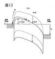
圖12是使用氧化物半導體形成的MOS電晶體的源極電極-汲極電極之間的帶結構的圖;12 is a diagram of the band structure between the source electrode and the drain electrode of a MOS transistor formed using an oxide semiconductor;
圖13是示出在圖12中對汲極電極一側施加正電壓的狀態的圖;FIG. 13 is a diagram showing a state in which a positive voltage is applied to the drain electrode side in FIG. 12;
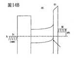
圖14A是示出使用氧化物半導體形成的MOS電晶體中的閘極電壓是正值時的MOS結構的能帶圖;圖14B是示出使用氧化物半導體形成的MOS電晶體中的閘極電壓是負值時的MOS結構的能帶圖;14A is an energy band diagram showing the MOS structure when the gate voltage in a MOS transistor formed using an oxide semiconductor is positive; FIG. 14B is an energy band diagram showing the gate voltage in a MOS transistor formed using an oxide semiconductor Band diagram of MOS structure when it is negative;
圖15是示出矽MOS電晶體的源極電極-汲極電極之間的帶結構的比較圖;15 is a comparative diagram showing the band structure between the source electrode and the drain electrode of the silicon MOS transistor;
圖16A和圖16B是示出本發明的一個實施例的等效電路圖;16A and 16B are equivalent circuit diagrams showing an embodiment of the present invention;
圖17是示出本發明的一個實施例的等效電路圖;以及FIG. 17 is an equivalent circuit diagram showing an embodiment of the present invention; and
圖18A至圖18E是示出電子設備的一個例子的圖。18A to 18E are diagrams showing an example of an electronic device.
下面,參照附圖對本發明的實施例模式進行詳細的說明。但是,本發明不侷限於以下說明,所屬技術領域的普通技術人員可以很容易地理解一個事實就是其方式及詳細內容可以被變換為各種各樣的形式。此外,本發明不應該被解釋為僅限定在以下實施例模式所記載的內容中。Hereinafter, an embodiment mode of the present invention will be described in detail with reference to the drawings. However, the present invention is not limited to the following description. A person of ordinary skill in the art can easily understand the fact that the method and details can be changed into various forms. In addition, the invention should notIt is interpreted as being limited to the content described in the following embodiment modes.
實施例模式1
在本實施例模式中,說明半導體積體電路的截面結構的一個例子。In this embodiment mode, an example of the cross-sectional structure of a semiconductor integrated circuit is described.
在本實施例模式中,使用圖1A至圖4B說明半導體積體電路及半導體積體電路的製造方法的一個實施例。In this embodiment mode, an embodiment of a semiconductor integrated circuit and a method of manufacturing the semiconductor integrated circuit will be described using FIGS. 1A to 4B.
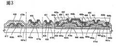
圖1A和圖1B示出半導體積體電路的截面結構的一個例子。圖1B所示的薄膜電晶體440是頂閘結構的薄膜電晶體之一。1A and 1B show an example of the cross-sectional structure of a semiconductor integrated circuit. The
薄膜電晶體440在具有絕緣表面的基板430上包括第一絕緣層447a、第二絕緣層443、第三絕緣層447b、氧化物半導體層442、第一源極電極層445a、第二源極電極層448a、第一汲極電極層445b、第二汲極電極層448b、閘極絕緣層444以及閘極電極層441。The
重疊於閘極電極層441的氧化物半導體層442的一部分是通道形成區,並且在氧化物半導體層442上彼此相鄰的第一源極電極層445a的下端部和第一汲極電極層445b的下端部的間隔寬度決定通道長度L1。A portion of the
此外,雖然使用單閘結構的薄膜電晶體說明薄膜電晶體440,但是也可以根據需要形成具有多個通道形成區的多閘結構的薄膜電晶體。In addition, although a single-gate structure thin film transistor is used to describe the
另外,也可以在同一製程中在與薄膜電晶體440相同的基板上形成寄生電容被降低了的薄膜電晶體470。In addition, the
下面,使用圖1A說明在基板430上製造薄膜電晶體440及薄膜電晶體470的製程。Hereinafter, the process of manufacturing the
對可以用於具有絕緣表面的基板430的基板沒有大限制,但是需要至少具有能夠承受後面的加熱處理的程度的耐熱性。可以使用鋇硼矽酸鹽玻璃、硼矽酸鋁玻璃等的玻璃基板。There is no major limitation on the substrate that can be used for the
另外,當後面的加熱處理的溫度較高時,最好使用應變點是730℃以上的玻璃基板。另外,作為玻璃基板,例如使用如鋁矽酸鹽玻璃、鋁硼矽酸鹽玻璃或鋇硼矽酸鹽玻璃等的玻璃材料。另外,藉由使基板材料相比氧化硼(B2O3)而含有更多的氧化鋇(BaO),可以獲得更實用的耐熱玻璃。因此,最好使用相比B2O3包含更多的BaO的玻璃基板。In addition, when the temperature of the subsequent heat treatment is high, it is better to use a glass substrate with a strain point of 730°C or higher. In addition, as the glass substrate, for example, a glass material such as aluminosilicate glass, aluminoborosilicate glass, or barium borosilicate glass is used. In addition, by making the substrate material contain more barium oxide (BaO) than boron oxide (B2O3), more practical heat-resistant glass can be obtained. Therefore, it is best to use a glass substrate containing more BaO than B2O3.
另外,還可以使用如陶瓷基板、石英基板、藍寶石基板等的由絕緣體構成的基板代替上述玻璃基板。此外,還可以使用晶化玻璃等。另外,也可以適當地使用其表面具有絕緣層的半導體基板、塑膠基板等。In addition, a substrate made of an insulator such as a ceramic substrate, a quartz substrate, a sapphire substrate, or the like may be used instead of the above-mentioned glass substrate. In addition, crystallized glass or the like can also be used. In addition, semiconductor substrates, plastic substrates, etc. having an insulating layer on the surface can also be suitably used.
首先,在具有絕緣表面的基板430上形成導電膜後,利用第一光微影製程形成電極層479a、479b、479c。作為電極層479a、479b、479c的材料,可以使用選自Al、Cr、Cu、Ta、Ti、Mo、W中的元素、以上述元素為成分的合金、組合上述元素的合金等。在本實施例模式中,電極層479a、479b、479c採用氮化鎢層和鎢層的疊層結構。First, after forming a conductive film on the
接著,形成覆蓋電極層479a、479b、479c的第一絕緣層447a。利用電漿CVD法或濺射法等並使用氧化矽層、氮化矽層、氧氮化矽層、氮氧化矽層的單層或疊層而形成第一絕緣層447a。Next, a first insulating
接著,在第一絕緣層447a上形成隔離絕緣層之後,利用第二光微影製程選擇性地進行去掉,以形成第二絕緣層443。利用電漿CVD法或濺射法等並使用氧化矽層、氮化矽層、氧氮化矽層或氮氧化矽層的單層或疊層而形成隔離絕緣層。將隔離絕緣層的膜厚度設定為500nm以上且2μm以下。此外,在同一製程中,在重疊於電極層479c的位置上形成成為隔離絕緣層的第五絕緣層473。如上所述,形成部分地厚的疊層區域和薄的單層區域。為了減少寄生電容,在膜厚度厚的區域中層疊作為隔離絕緣層的第四絕緣層和第一絕緣層,並且為了形成儲存電容器等,在膜厚度薄的區域中設置第一絕緣層。Next, after the isolation insulating layer is formed on the first insulating
接著,形成覆蓋第一絕緣層447a、第二絕緣層443、第五絕緣層473的第三絕緣層447b。作為接觸於氧化物半導體層的第三絕緣層447b,最好使用氧化矽層、氧氮化矽層、氧化鋁層或氧氮化鋁層等的氧化物絕緣層。作為第三絕緣層447b的形成方法,可以使用電漿CVD法或者濺射法等,但是為了不使第三絕緣層447b中包含大量的氫,最好利用濺射法來形成第三絕緣層447b。Next, a third
在本實施例模式中,利用濺射法形成氧化矽層作為第三絕緣層447b。將基板430搬送到處理室,引入包括去掉了氫及水分的高純度氧的濺射氣體並使用矽靶,以在基板430上形成氧化矽層作為第三絕緣層447b。此外,基板430的溫度可以是室溫,也可以加熱基板430。In this embodiment mode, a silicon oxide layer is formed as the third insulating
例如,在如下條件下形成氧化矽層:使用石英(最好是合成石英);基板溫度是108℃;基板與靶之間的距離(T-S間距離)是60mm;壓力是0.4Pa;高頻電源是1.5kW;在氧及氬(氧流量是25sccm,氬流量是25sccm)氣圍下;利用RF濺射法。將氧化矽層的厚度設定為100nm。另外,可以將矽靶用作用來形成氧化矽層的靶代替石英(最好是合成石英)。另外,作為濺射氣體,使用氧或者氧及氬的混合氣體。For example, the silicon oxide layer is formed under the following conditions: using quartz (preferably synthetic quartz); the substrate temperature is 108°C; the distance between the substrate and the target (distance between TS) is 60mm; the pressure is 0.4Pa; high-frequency power supply It is 1.5kW; under oxygen and argon (oxygen flow rate is 25sccm, argon flow rate is 25sccm); RF sputtering method is used. The thickness of the silicon oxide layer is set to 100 nm. In addition, a silicon target can be used as a target for forming a silicon oxide layer instead of quartz (preferably synthetic quartz). In addition, as the sputtering gas, oxygen or a mixed gas of oxygen and argon is used.
此時,最好去除處理室內的殘留水分並形成第三絕緣層447b。這是因為不使第三絕緣層447b包含氫、羥基或水分的緣故。At this time, it is preferable to remove residual moisture in the processing chamber and form the third insulating
為了去除處理室內的殘留水分,最好使用吸附型真空泵。例如,最好使用低溫泵、離子泵、鈦昇華泵。此外,作為排氣單元,也可以對渦輪泵追加冷捕集器。因為在使用低溫泵進行排氣的沉積室中例如排出氫原子、水(H2O)等的包括氫原子的化合物等,所以可以降低在該處理室形成的第三絕緣層447b所包含的雜質的濃度。In order to remove residual moisture in the processing chamber, it is best to use an adsorption-type vacuum pump. For example, it is best to use cryogenic pumps, ion pumps, and titanium sublimation pumps. In addition, as an exhaust unit, a cold trap may be added to the turbo pump. In the deposition chamber where the cryopump is used for exhausting, for example, hydrogen atoms, water (H2O) and other compounds including hydrogen atoms are discharged, so the concentration of impurities contained in the third insulating
作為濺射法,有作為濺射電源使用高頻電源的RF濺射法、使用直流電源的DC濺射法,並且還有以脈衝方式施加偏壓的脈衝DC濺射法。RF濺射法主要用於絕緣膜的形成,而DC濺射法主要用於金屬膜的形成。As the sputtering method, there are an RF sputtering method that uses a high-frequency power source as a sputtering power source, a DC sputtering method that uses a DC power source, and a pulsed DC sputtering method that applies a bias voltage in a pulsed manner. The RF sputtering method is mainly used for the formation of insulating films, and the DC sputtering method is mainly used for the formation of metal films.
此外,還有可以設置多個材料不同的靶的多元濺射裝置。多元濺射裝置既可以在同一處理室中層疊形成不同材料的膜,又可以在同一處理室中使多種材料同時放電而進行成膜。In addition, there is also a multi-element sputtering device that can set multiple targets of different materials. The multi-element sputtering device can not only laminate and form films of different materials in the same processing chamber, but also discharge multiple materials in the same processing chamber to form films.
此外,有利用如下濺射法的濺射裝置,該濺射法是:在處理室內具備磁體機構的磁控管濺射法;以及不使用輝光放電而利用使用微波來產生的電漿的ECR濺射法。In addition, there are sputtering devices that use the following sputtering method: a magnetron sputtering method equipped with a magnet mechanism in a processing chamber; and an ECR sputtering method that uses plasma generated using microwaves instead of glow discharge Shooting.
此外,作為使用濺射法的成膜方法,還有:在形成膜時使靶物質與濺射氣體成分產生化學反應而形成它們的化合物薄膜的反應濺射法;以及在形成膜時對基板也施加電壓的偏壓濺射法。In addition, as a film forming method using a sputtering method, there are: a reactive sputtering method in which a target substance and a sputtering gas component are chemically reacted to form a thin film of their compound during film formation; Bias sputtering method with applied voltage.
此外,第三絕緣層447b也可以具有疊層結構,例如,也可以採用如下疊層結構,在該疊層結構中從基板430一側層疊有氮化矽層、氮氧化矽層或氮化鋁層等的氮化物絕緣層和上述氧化物絕緣層。In addition, the third insulating
例如,引入包含去除了氫及水分的高純度氮的濺射氣體並使用矽靶,而在氧化矽層和基板之間形成氮化矽層。在此情況下也與氧化矽層同樣,最好去除處理室內的殘留水分並形成氮化矽層。For example, a sputtering gas containing high-purity nitrogen from which hydrogen and moisture have been removed is introduced and a silicon target is used to form a silicon nitride layer between the silicon oxide layer and the substrate. In this case, as with the silicon oxide layer, it is better to remove residual moisture in the processing chamber and form a silicon nitride layer.
在形成氮化矽層的情況下,也可以在形成膜時加熱基板。In the case of forming a silicon nitride layer, the substrate may be heated when the film is formed.
當層疊氮化矽層和氧化矽層作為第三絕緣層447b時,可以在同一處理室內使用共用的矽靶來形成氮化矽層和氧化矽層。首先,引入包含氮的濺射氣體,使用安裝在處理室內的矽靶來形成氮化矽層,接著將濺射氣體轉換到包含氧的濺射氣體並使用同一矽靶來形成氧化矽層。因為可以不使暴露於大氣地連續形成氮化矽層和氧化矽層,所以可以防止氫、水分等雜質吸附到氮化矽層的表面。When a silicon nitride layer and a silicon oxide layer are laminated as the third insulating
接著,在第三絕緣層447b上形成膜厚度為2nm以上且200nm以下的氧化物半導體膜。Next, an oxide semiconductor film having a film thickness of 2 nm or more and 200 nm or less is formed on the third insulating
此外,為了盡可能地不使氧化物半導體膜包含氫、羥基以及水分,最好在濺射裝置的預熱室中對形成有第三絕緣層447b的基板430進行預熱,而使吸附到基板430的氫、水分等的雜質脫離並將其排出,作為成膜之前的處理。另外,作為設置在預熱室內的排氣單元,最好使用低溫泵。注意,也可以省略該預熱處理。In addition, in order to prevent the oxide semiconductor film from containing hydrogen, hydroxyl, and moisture as much as possible, it is preferable to preheat the
另外,最好在利用濺射法形成氧化物半導體膜之前,進行引入氬氣體來產生電漿的反濺射,以去除吸附到第三絕緣層447b表面的塵屑。在反濺射中,不對靶一側施加電壓而在氬氣圍下使用高頻電源對基板一側施加電壓,在基板附近形成電漿,而進行表面改性。另外,也可以使用氮、氦、氧等代替氬氣圍。In addition, it is preferable to perform reverse sputtering in which argon gas is introduced to generate plasma before forming the oxide semiconductor film by the sputtering method to remove dust adsorbed on the surface of the third insulating
氧化物半導體膜藉由濺射法來形成。作為氧化物半導體膜,使用In-Ga-Zn-O類、In-Sn-Zn-O類、In-Al-Zn-O類、Sn-Ga-Zn-O類、Al-Ga-Zn-O類、Sn-Al-Zn-O類、In-Zn-O類、Sn-Zn-O類、Al-Zn-O類、In-O類、Sn-O類、Zn-O類的氧化物半導體膜。在本實施例模式中,使用用來形成In-Ga-Zn-O類氧化物半導體膜的靶並利用濺射法來形成氧化物半導體膜。此外,氧化物半導體膜可以在稀有氣體(典型為氬)氣圍下、氧氣圍下或者稀有氣體(典型為氬)及氧的混合氣圍下利用濺射法來形成。此外,在利用濺射法時,也可以使用包括2wt%以上且10wt%以下的SiO2的靶來形成膜。The oxide semiconductor film is formed by a sputtering method. As the oxide semiconductor film, In-Ga-Zn-O type, In-Sn-Zn-O type, In-Al-Zn-O type, Sn-Ga-Zn-O type, Al-Ga-Zn-O type Type, Sn-Al-Zn-O type, In-Zn-O type, Sn-Zn-O type, Al-Zn-O type, In-O type, Sn-O type, Zn-O type oxide semiconductor membrane. In this embodiment mode, a target for forming an In-Ga-Zn-O-based oxide semiconductor film is used and sputtering is usedThe oxide semiconductor film is formed by the injection method. In addition, the oxide semiconductor film can be formed by a sputtering method under a rare gas (typically argon) atmosphere, an oxygen atmosphere, or a rare gas (typically argon) and oxygen atmosphere. In addition, when the sputtering method is used, a target including SiO 2 of 2 wt% or more and 10 wt% or less may be used to form the film.
作為利用濺射法來製造氧化物半導體膜的靶,可以使用以氧化鋅為主要成分的金屬氧化物的靶。此外,作為金屬氧化物的靶的其他例子,可以使用包含In、Ga及Zn的用來形成氧化物半導體膜的靶(組成比是In2O3:Ga2O3:ZnO=1:1:1[mol數比])。此外,作為包括In、Ga及Zn的用來形成氧化物半導體膜的靶,也可以使用具有In2O3:Ga2O3:ZnO=1:1:2[mol數比]、或者In2O3:Ga2O3:ZnO=1:1:4[mol數比]的組成比的靶。用來形成氧化物半導體膜的靶的填充率是90%以上且100%以下,最好是95%以上且99.9%以下。藉由使用填充率高的用來形成氧化物半導體膜的靶,可以形成緻密的氧化物半導體膜。As a target for producing an oxide semiconductor film by a sputtering method, a target of a metal oxide containing zinc oxide as a main component can be used. In addition, as another example of a metal oxide target, a target for forming an oxide semiconductor film containing In, Ga, and Zn can be used (the composition ratio is In2O3:Ga2O3:ZnO=1:1:1 [mole ratio] ). In addition, as a target for forming an oxide semiconductor film including In, Ga, and Zn, it is also possible to use In2O3:Ga2O3:ZnO=1:1:2 [mole ratio], or In2O3:Ga2O3:ZnO=1: Target with a composition ratio of 1:4 [mol ratio]. The filling rate of the target for forming the oxide semiconductor film is 90% or more and 100% or less, preferably 95% or more and 99.9% or less. By using a target for forming an oxide semiconductor film with a high filling rate, a dense oxide semiconductor film can be formed.
在保持為減壓狀態的處理室內保持基板,去除處理室內的殘留水分並引入被去除了氫及水分的濺射氣體,將金屬氧化物用作靶,在基板430上形成氧化物半導體膜。為了去除處理室內的殘留水分,最好使用吸附型真空泵。例如,最好使用低溫泵、離子泵、鈦昇華泵。此外,作為排氣單元,也可以對渦輪泵追加冷捕集器。因為當使用低溫泵對沉積室進行排氣時,例如排出氫原子、水(H2O)等的包含氫原子的化合物(最好也排出包含碳原子的化合物)等,所以可以降低形成在該沉積室內的氧化物半導體膜所包含的雜質的濃度。此外,也可以在形成氧化物半導體膜時加熱基板。The substrate is held in a processing chamber maintained in a reduced pressure state, residual moisture in the processing chamber is removed, and a sputtering gas from which hydrogen and moisture have been removed is introduced. The metal oxide is used as a target to form an oxide semiconductor film on the
例如,在如下條件下形成氧化物半導體膜,該條件是:基板溫度是室溫;基板與靶之間的距離是60mm;壓力是0.4Pa;直流(DC)電源是0.5kW;氧及氬(氧流量是15sccm,氬流量是30sccm)氣圍下。注意,當使用脈衝直流(DC)電源時,可以減輕當形成膜時產生的粉狀物質(也稱為微粒、塵屑)且膜厚度分佈也均勻,所以是較佳的。最好將氧化物半導體膜的膜厚度設定為5nm以上且30nm以下。注意,每個氧化物半導體材料分別具有不同的合適厚度,因此根據所使用的氧化物半導體材料適當地選擇膜厚度,即可。For example, an oxide semiconductor film is formed under the following conditions: the substrate temperature is room temperature; the distance between the substrate and the target is 60 mm; the pressure is 0.4 Pa; the direct current (DC) power supply is 0.5 kW; oxygen and argon ( The oxygen flow rate is 15 sccm and the argon flow rate is 30 sccm). Note that when a pulsed direct current (DC) power supply is used, it is possible to reduce the powdery substances (also called particles, dust) generated when the film is formed and the film thickness distribution is also uniform, so it is preferable. It is preferable to set the film thickness of the oxide semiconductor film to be 5 nm or more and 30 nm or less. Note that each oxide semiconductor material has a different appropriate thickness, so the film thickness may be appropriately selected according to the oxide semiconductor material used.
接著,進行第三光微影製程將氧化物半導體膜加工為島狀的氧化物半導體層442、472(參照圖1A)。另外,還可以使用噴墨法形成用來形成島狀的氧化物半導體層442、472的抗蝕劑掩模。當藉由噴墨法形成抗蝕劑掩模時不使用光掩模,因此可以縮減製造成本。Next, a third photolithography process is performed to process the oxide semiconductor film into island-shaped oxide semiconductor layers 442 and 472 (see FIG. 1A). In addition, a resist mask for forming the island-shaped oxide semiconductor layers 442 and 472 can also be formed using an inkjet method. When the resist mask is formed by the inkjet method, a photomask is not used, so the manufacturing cost can be reduced.
注意,在此進行的對氧化物半導體膜的蝕刻可以是乾蝕刻或濕蝕刻,並且還可以使用乾蝕刻和濕蝕刻的兩者。Note that the etching of the oxide semiconductor film performed here may be dry etching or wet etching, and both dry etching and wet etching may also be used.
作為用於乾蝕刻的蝕刻氣體,最好使用含有氯的氣體(氯類氣體,例如氯(Cl2)、氯化硼(BCl3)、氯化矽(SiCl4)、四氯化碳(CCl4)等)。As an etching gas for dry etching, it is preferable to use a gas containing chlorine (chlorine-based gas, such as chlorine (Cl2), boron chloride (BCl3), silicon chloride (SiCl4), carbon tetrachloride (CCl4), etc.) .
另外,還可以使用含有氟的氣體(氟類氣體,例如四氟化碳(CF4)、六氟化硫(SF6)、三氟化氮(NF3)、三氟甲烷(CHF3)等)、溴化氫(HBr)、氧(O2)或對上述氣體添加了氦(He)或氬(Ar)等的稀有氣體的氣體等。In addition, you can also use fluorine-containing gas (fluorine-based gas, such as carbon tetrafluoride (CF4), sulfur hexafluoride (SF6), nitrogen trifluoride (NF3), trifluoromethane (CHF3), etc.), bromination Hydrogen (HBr), oxygen (O2), or a gas in which a rare gas such as helium (He) or argon (Ar) is added to the above gas.
作為乾蝕刻法,可以使用平行平板型RIE(Reactive Ion Etching:反應性離子蝕刻)法或ICP(Inductively Coupled Plasma:感應耦合電漿)蝕刻法。為了將氧化物半導體膜蝕刻為所希望的形狀,適當地調節蝕刻條件(對線圈型的電極施加的電量、對基板一側的電極施加的電量、基板一側的電極溫度等)。As the dry etching method, a parallel plate type RIE (Reactive Ion Etching) method or an ICP (Inductively Coupled Plasma) etching method can be used. In order to etch the oxide semiconductor film into a desired shape, the etching conditions (the amount of electricity applied to the coil-shaped electrode, the amount of electricity applied to the electrode on the substrate side, the temperature of the electrode on the substrate side, etc.) are appropriately adjusted.
作為用於濕蝕刻的蝕刻液,可以使用將磷酸、醋酸以及硝酸混合的溶液、過氧化氫氨水(31wt%的過氧化氫水:28wt%的氨水:水=5:2:2)等。此外,還可以使用ITO07N(日本關東化學株式會社製造)。As an etching solution used for wet etching, a solution in which phosphoric acid, acetic acid, and nitric acid are mixed, hydrogen peroxide ammonia water (31 wt% hydrogen peroxide water: 28 wt% ammonia water: water=5:2:2) can be used. In addition, ITO07N (manufactured by Kanto Chemical Co., Ltd.) can also be used.
此外,藉由清洗去除濕蝕刻後的蝕刻液以及被蝕刻掉的材料。也可以提純包括該被去除了的材料的蝕刻液的廢液,來再使用所包含的材料。藉由從該蝕刻後的廢液回收包含在氧化物半導體層中的銦等的材料並將它再使用,可以高效地使用資源並實現低成本化。In addition, the etching solution after wet etching and the etched material are removed by cleaning. It is also possible to purify the waste liquid of the etching liquid including the removed material to reuse the contained material. By recovering materials such as indium contained in the oxide semiconductor layer from the waste liquid after etching and reusing it, resources can be used efficiently and cost reduction can be achieved.
根據材料而適當地調節蝕刻條件(蝕刻液、蝕刻時間以及溫度等),以便可以將氧化物半導體膜蝕刻為所希望的加工形狀。The etching conditions (etching liquid, etching time, temperature, etc.) are appropriately adjusted according to the material so that the oxide semiconductor film can be etched into a desired processing shape.
在本實施例模式中,藉由將混合磷酸、醋酸以及硝酸而成的溶液用作蝕刻液的濕蝕刻法,將氧化物半導體膜加工為島狀的氧化物半導體層442、472。In this embodiment mode, by mixing phosphoric acid, acetic acid and nitric acidThe resulting solution is used as a wet etching method of an etchant to process the oxide semiconductor film into island-shaped oxide semiconductor layers 442 and 472.
在本實施例模式中,對氧化物半導體層442、472進行第一加熱處理。將第一加熱處理的溫度設定為400℃以上且750℃以下,最好設定為400℃以上且低於基板的應變點的溫度。在此,將基板放入到加熱處理裝置之一的電爐,在氮氣圍下以450℃對氧化物半導體層進行1小時的加熱處理。然後,以不使接觸於大氣並防止水、氫再混入到氧化物半導體層的方式得到氧化物半導體層。藉由該第一加熱處理,可以對氧化物半導體層442、472進行脫水化或脫氫化。In this embodiment mode, the oxide semiconductor layers 442 and 472 are subjected to the first heat treatment. The temperature of the first heat treatment is set to 400°C or higher and 750°C or lower, preferably 400°C or higher and lower than the strain point of the substrate. Here, the substrate is placed in an electric furnace, which is one of the heat treatment devices, and the oxide semiconductor layer is heated at 450° C. for 1 hour under a nitrogen atmosphere. Then, the oxide semiconductor layer is obtained so as not to expose it to the atmosphere and to prevent water and hydrogen from being mixed into the oxide semiconductor layer. By this first heat treatment, the oxide semiconductor layers 442 and 472 can be dehydrated or dehydrogenated.
注意,加熱處理裝置不侷限於電爐,也可以具備利用由電阻發熱體等發熱體的熱傳導或熱輻射來加熱被處理物的裝置。例如,可以使用GRTA(Gas Rapid Thermal Anneal:氣體快速熱退火)裝置、LRTA(Lamp Rapid Thermal Anneal:燈快速熱退火)裝置等的RTA(Rapid Thermal Anneal:快速熱退火)裝置。LRTA裝置是藉由鹵素燈、金鹵燈、氙弧燈、碳弧燈、高壓鈉燈或者高壓汞燈等的燈所發射的光(電磁波)的輻射來加熱被處理物的裝置。GRTA裝置是使用高溫的氣體進行加熱處理的裝置。作為氣體,使用氬等的惰性氣體或者氮等的即使進行加熱處理也不與被處理物產生反應的稀有氣體。Note that the heat treatment device is not limited to an electric furnace, and may be provided with a device that uses heat conduction or heat radiation from a heating element such as a resistance heating element to heat the object to be processed. For example, RTA (Rapid Thermal Anneal) devices such as GRTA (Gas Rapid Thermal Anneal) devices and LRTA (Lamp Rapid Thermal Anneal) devices can be used. The LRTA device is a device that heats the object to be processed by the radiation of light (electromagnetic waves) emitted by lamps such as halogen lamps, metal halide lamps, xenon arc lamps, carbon arc lamps, high pressure sodium lamps, or high pressure mercury lamps. GRTA device is a device that uses high-temperature gas for heat treatment. As the gas, an inert gas such as argon or a rare gas such as nitrogen that does not react with the object to be processed even if the heat treatment is performed is used.
例如,作為第一加熱處理,也可以進行如下GRTA,在該GRTA中,將基板移動到加熱為650℃至700℃的高溫的惰性氣體中,加熱幾分鐘,然後將基板從加熱為高溫的惰性氣體中移動。當採用GRTA時,可以進行短時間內的高溫加熱處理。For example, as the first heating treatment, the following GRTA may also be performed, in which the substrate is moved to a temperature of 650°C to 700°C.In a warm inert gas, heat for a few minutes, and then move the substrate from the inert gas heated to a high temperature. When GRTA is used, high temperature heat treatment can be performed in a short time.
另外,在第一加熱處理中,最好氮或氦、氖、氬等的稀有氣體不包含水、氫等。另外,最好將引入加熱處理裝置中的氮或氦、氖、氬等的稀有氣體的純度設定為6N(99.9999%)以上,更佳地設定為7N(99.99999%)以上(即,將雜質濃度設定為1ppm以下,最好設定為0.1ppm以下)。In addition, in the first heat treatment, it is preferable that a rare gas such as nitrogen, helium, neon, and argon does not contain water, hydrogen, or the like. In addition, it is better to set the purity of the rare gas such as nitrogen or helium, neon, argon, etc., introduced into the heat treatment device to 6N (99.9999%) or more, more preferably to 7N (99.99999%) or more (that is, the impurity concentration Set to 1 ppm or less, preferably 0.1 ppm or less).
另外,根據第一加熱處理的條件或氧化物半導體層的材料,有時氧化物半導體層晶化而成為微晶膜或多晶膜。例如,有時成為晶化率是90%以上或80%以上的微晶氧化物半導體膜。此外,根據第一加熱處理的條件或氧化物半導體層的材料,有時成為不包含結晶成分的非晶氧化物半導體膜。此外,有時成為在非晶氧化物半導體中混合有微晶部(粒徑是1nm以上且20nm以下(典型是2nm以上且4nm以下))的氧化物半導體膜。In addition, depending on the conditions of the first heat treatment or the material of the oxide semiconductor layer, the oxide semiconductor layer may be crystallized to become a microcrystalline film or a polycrystalline film. For example, it may become a microcrystalline oxide semiconductor film with a crystallization rate of 90% or more or 80% or more. In addition, depending on the conditions of the first heat treatment or the material of the oxide semiconductor layer, it may become an amorphous oxide semiconductor film that does not contain crystalline components. In addition, it may be an oxide semiconductor film in which microcrystalline parts (grain diameters of 1 nm or more and 20 nm or less (typically 2 nm or more and 4 nm or less)) are mixed in an amorphous oxide semiconductor.
另外,也可以對加工成島狀氧化物半導體層之前的氧化物半導體膜進行對氧化物半導體層的第一加熱處理。在此情況下,在第一加熱處理之後從加熱裝置拿出基板,進行光微影製程。In addition, the oxide semiconductor film before being processed into the island-shaped oxide semiconductor layer may be subjected to the first heat treatment of the oxide semiconductor layer. In this case, after the first heat treatment, the substrate is taken out from the heating device, and the photolithography process is performed.
具有對氧化物半導體層的脫水化或脫氫化的效果的加熱處理可以進行在形成氧化物半導體層後、在氧化物半導體層上層疊源極電極及汲極電極後、或者在源極電極及汲極電極上形成閘極絕緣層後。The heat treatment having the effect of dehydration or dehydrogenation of the oxide semiconductor layer can be performed after the oxide semiconductor layer is formed, the source electrode and the drain electrode are laminated on the oxide semiconductor layer, or the source electrode and the drain electrodeAfter forming a gate insulating layer on the electrode.
但是,只要在形成膜時可以得到氫或水分被充分地降低而被高純度化的氧化物半導體層,就也可以不進行第一加熱處理。在形成膜時得到氫或水分被充分地降低而被高純度化的氧化物半導體層的情況下,將基板保持在保持為減壓狀態的處理室內,將基板加熱到室溫以上且低於400℃的溫度。然後,去除處理室內的殘留水分並引入被去除了氫及水分的濺射氣體,將金屬氧化物用於靶,以在基板上形成氧化物半導體層。因為使用低溫泵進行排氣的沉積室例如排出氫原子、水(H2O)等的包含氫原子的化合物(最好也排出包含碳原子的化合物)等,所以可以降低在該沉積室內形成的氧化物半導體層所包含的雜質濃度。藉由利用低溫泵去除殘留在處理室內的水分並進行濺射成膜,可以將形成氧化物半導體層時的基板溫度設定為室溫至低於400℃的溫度。However, as long as it is possible to obtain an oxide semiconductor layer in which hydrogen or moisture has been sufficiently reduced to be highly purified when the film is formed, the first heat treatment may not be performed. In the case of obtaining an oxide semiconductor layer in which hydrogen or moisture has been sufficiently reduced during film formation to be highly purified, the substrate is held in a processing chamber maintained at a reduced pressure, and the substrate is heated to room temperature or higher and lower than 400 ℃ temperature. Then, the residual moisture in the processing chamber is removed and the sputtering gas from which hydrogen and moisture have been removed is introduced, and the metal oxide is used as the target to form an oxide semiconductor layer on the substrate. Since the deposition chamber that uses cryopumps to exhaust, for example, hydrogen atoms, water (H2O) and other hydrogen atom-containing compounds (preferably also carbon atom-containing compounds) are discharged, the oxides formed in the deposition chamber can be reduced The concentration of impurities contained in the semiconductor layer. By using a cryopump to remove moisture remaining in the processing chamber and perform sputtering film formation, the substrate temperature when forming the oxide semiconductor layer can be set to a temperature from room temperature to less than 400°C.
接著,藉由第四光微影製程在第三絕緣層447b上形成抗蝕劑掩模,選擇性地進行蝕刻,以形成到達電極層479a的開口。Next, a resist mask is formed on the third insulating
接著,在第三絕緣層447b及氧化物半導體層442、472上形成導電膜。藉由濺射法、真空蒸鍍法形成導電膜即可。作為導電膜的材料,可以舉出選自Al、Cr、Cu、Ta、Ti、Mo、W中的元素、以上述元素為成分的合金、組合上述元素的合金膜等。此外,也可以使用選自錳、鎂、鋯、鈹、釷中的任一種或多種的材料。此外,金屬導電膜可以採用單層結構、兩層以上的疊層結構。例如,可以舉出:包含矽的鋁膜的單層結構;在鋁膜上層疊鈦膜的兩層結構;Ti膜、該Ti膜上層疊的鋁膜、其上形成的Ti膜的三層結構等。此外,也可以採用將Al與選自鈦(Ti)、鉭(Ta)、鎢(W)、鉬(Mo)、鉻(Cr)、釹(Nd)、鈧(Sc)中的一種或多種元素組合起來的膜、合金膜、氮化膜。在本實施例模式中,形成鈦膜(膜厚度為10nm以上且100nm以下)和鋁膜(膜厚度為20nm以上且500nm以下)的疊層膜作為導電膜。Next, a conductive film is formed on the third insulating
接著,利用電漿CVD法或濺射法等並利用氧化矽層、氮化矽層、氧氮化矽層、氮氧化矽層的單層或疊層來在導電膜上形成膜厚度是200nm以上且2000nm以下的絕緣膜。Next, a single layer or a stack of silicon oxide layer, silicon nitride layer, silicon oxynitride layer, and silicon oxynitride layer is used to form a film thickness of 200 nm or more on the conductive film by plasma CVD method or sputtering method. And the insulating film below 2000nm.
接著,藉由第五光微影製程在絕緣膜上形成抗蝕劑掩模,選擇性地進行蝕刻來形成第四絕緣層446、第一源極電極層445a、第二源極電極層448a、第一汲極電極層445b、第二汲極電極層448b,然後去除抗蝕劑掩模。此外,為了降低與後面形成的閘極電極層之間的寄生電容,設置有第四絕緣層446。另外,當所形成的源極電極層、汲極電極層的端部是錐形形狀時,層疊在其上的閘極絕緣層的覆蓋性提高,所以是較佳的。Next, a resist mask is formed on the insulating film by a fifth photolithography process, and etching is selectively performed to form the fourth insulating
注意,當對導電膜進行蝕刻時,以不去除氧化物半導體層442、472並不使其下的第三絕緣層447b露出的方式適當地調節各材料及蝕刻條件。Note that when the conductive film is etched, the materials and etching conditions are appropriately adjusted so that the oxide semiconductor layers 442 and 472 are not removed and the third insulating
在本實施例模式中,作為第一源極電極層445a及第一汲極電極層445b使用Ti膜,作為第二源極電極層448a及第二汲極電極層448b使用鋁膜,作為氧化物半導體層442使用In-Ga-Zn-O類氧化物,並且作為蝕刻劑使用過氧化氫氨水(氨水、水、過氧化氫水的混合液)。In this embodiment mode, a Ti film is used as the first
注意,在第五光微影製程中,氧化物半導體層442有時僅有一部分被蝕刻,而成為包括槽部(凹部)的氧化物半導體層。此外,也可以藉由噴墨法形成用來形成第一源極電極層445a及第一汲極電極層445b的抗蝕劑掩模。當藉由噴墨法形成抗蝕劑掩模時,不使用光掩模,所以可以降低製造成本。Note that in the fifth photolithography process, sometimes only a part of the
作為在第五光微影製程中的形成抗蝕劑掩模時的曝光,利用紫外線、KrF雷射、ArF雷射。在氧化物半導體層442上彼此相鄰的源極電極層的下端部和汲極電極層的下端部的間隔寬度決定後面形成的薄膜電晶體440的通道長度L1。另外,當以使通道長度L1小於25nm的方式進行曝光時,使用其波長極短即幾nm至幾十nm的超紫外線(Extreme Ultraviolet)來進行在第五光微影製程中的形成抗蝕劑掩模時的曝光。利用超紫外線的曝光具有如下特點,即解析度高且焦點深度也大。因此,也可以將後面形成的薄膜電晶體440的通道長度L1設定為10nm以上且1000nm以下,可以使電路的工作速度高速化。並且,因為截止電流值極為小,所以也可以實現低耗電量化。As the exposure when forming the resist mask in the fifth photolithography process, ultraviolet rays, KrF laser, and ArF laser are used. The interval width between the lower end of the source electrode layer and the lower end of the drain electrode layer adjacent to each other on the
接著,在第四絕緣層446、氧化物半導體層442、472、第一源極電極層445a、第二源極電極層448a、第一汲極電極層445b以及第二汲極電極層448b上形成閘極絕緣層444。Next, in the fourth insulating
藉由利用電漿CVD法或濺射法等並利用氧化矽層、氮化矽層、氧氮化矽層、氮氧化矽層或者氧化鋁層的單層或疊層來形成閘極絕緣層444。另外,為了不使閘極絕緣層444中包含大量的氫,最好藉由濺射法形成閘極絕緣層444。當藉由濺射法形成氧化矽膜時,作為靶使用矽靶或石英靶,並且作為濺射氣體使用氧、或者氧及氬的混合氣體。The
閘極絕緣層444也可以採用從第二源極電極層448a及第二汲極電極層448b一側層疊氧化矽層和氮化矽層的結構。例如,也可以形成膜厚度是5nm以上且300nm以下的氧化矽層(SiOx(x>0))作為第一閘極絕緣層,並在第一閘極絕緣層上藉由濺射法層疊膜厚度是50nm以上且200nm以下的氮化矽層(SiNy(y>0))作為第二閘極絕緣層,以得到膜厚度是100nm的閘極絕緣層。在本實施例模式中,在如下條件下形成膜厚度是100nm的氧化矽層,該條件是:壓力是0.4Pa;高頻電源是1.5kW;氧及氬(氧流量是25sccm,氬流量是25sccm)氣圍下;利用RF濺射法。The
接著,藉由第六光微影製程形成抗蝕劑掩模,選擇性地進行蝕刻來去除閘極絕緣層444及第四絕緣層446的一部分,以形成到達薄膜電晶體470的源極電極層或汲極電極層的開口。Next, a resist mask is formed by a sixth photolithography process, and etching is selectively performed to remove part of the
接著,在閘極絕緣層444及開口上形成導電膜,然後藉由第七光微影製程形成閘極電極層441、471、佈線層474a、474b。另外,也可以藉由噴墨法形成抗蝕劑掩模。因為當噴墨法形成抗蝕劑掩模時不使用光掩模,所以可以縮減製造成本。Next, a conductive film is formed on the
此外,閘極電極層441、471、佈線層474a、474b可以使用鉬、鈦、鉻、鉭、鎢、鋁、銅、釹、鈧等的金屬材料或者以這些金屬材料為主要成分的合金材料的單層或疊層而形成。In addition, the gate electrode layers 441, 471, and the
例如,作為閘極電極層441、471、佈線層474a、474b的兩層的疊層結構,最好採用:在鋁層上層疊有鉬層的兩層的疊層結構;在銅層上層疊有鉬層的兩層結構;在銅層上層疊有氮化鈦層或氮化鉭層的兩層結構;層疊氮化鈦層和鉬層的兩層結構。作為三層的疊層結構,最好採用:層疊有鎢層或氮化鎢層、鋁和矽的合金或者鋁和鈦的合金、氮化鈦或者鈦層的三層結構。注意,也可以使用具有透光性的導電膜來形成閘極電極層。作為具有透光性的導電膜的例子,可以舉出透光導電氧化物等。For example, as a two-layer laminated structure of the gate electrode layers 441, 471 and the
在本實施例模式中,藉由濺射法形成膜厚度是150nm的鎢膜作為閘極電極層441、471、佈線層474a、474b。In this embodiment mode, a tungsten film with a film thickness of 150 nm is formed by a sputtering method as the gate electrode layers 441 and 471 and the
接著,在惰性氣體氣圍下或氧氣體氣圍下進行第二加熱處理(最好是200℃以上且400℃以下,例如是250℃以上且350℃以下)。在本實施例模式中,在氮氣圍下以250℃進行1小時的第二加熱處理。此外,也可以在薄膜電晶體440、470上形成保護絕緣層、平坦化絕緣層後進行第二加熱處理。Next, the second heat treatment is performed under an inert gas enclosure or an oxygen gas enclosure (preferably 200°C or higher and 400°C or lower, for example, 250°C or higher and 350°C or lower). In this embodiment mode, under nitrogenThe second heat treatment was performed at 250°C for 1 hour. In addition, a protective insulating layer and a planarizing insulating layer may be formed on the
再者,也可以在大氣中以100℃以上且200℃以下的溫度進行1小時以上且30小時以下的加熱處理。在該加熱處理中,既可以保持一定的加熱溫度來加熱,又可以反復從室溫到100℃以上且200℃以下的加熱溫度的升溫和從加熱溫度到室溫的降溫多次。此外,也可以在形成氧化物絕緣層之前在減壓下進行該加熱處理。當在減壓下進行加熱處理時,可以縮短加熱處理。In addition, the heat treatment may be performed in the atmosphere at a temperature of 100°C or higher and 200°C or lower for 1 hour or longer and 30 hours or shorter. In this heat treatment, heating can be performed while maintaining a constant heating temperature, and the temperature increase from room temperature to 100°C or more and 200°C or less and the temperature drop from the heating temperature to room temperature can be repeated many times. In addition, this heat treatment may be performed under reduced pressure before forming the oxide insulating layer. When the heat treatment is performed under reduced pressure, the heat treatment can be shortened.
藉由上述製程,可以形成具有氫、水分、氫化物、氫氧化物的濃度被降低了的氧化物半導體層442、472的薄膜電晶體440、470(參照圖1B)。Through the above process,
利用第五絕緣層473而與電極層479c之間的寄生電容降低了的薄膜電晶體470包括第三源極電極層475a、第四源極電極層478a、第三汲極電極層475b以及第四汲極電極層478b。另外,重疊於第五絕緣層473的電極層479c是閘極信號線,示出與第四汲極電極層478b的佈線交叉部的結構。此外,第三源極電極層475a電連接到電極層479a。此外,第四源極電極層478a電連接到佈線層474a。此外,薄膜電晶體470的通道長度L2長於薄膜電晶體440的通道長度L1,並且薄膜電晶體470是截止電流值小的薄膜電晶體。The
此外,也可以在薄膜電晶體440、470上設置保護絕緣層、用於平坦化的平坦化絕緣層。例如,也可以形成氧化矽層、氮化矽層、氧氮化矽層、氮氧化矽層或者氧化鋁層的單層或疊層作為保護絕緣層。In addition, protective insulation can also be provided on the
此外,作為平坦化絕緣層,可以使用具有耐熱性的有機材料如聚醯亞胺、丙烯酸樹脂、苯並環丁烯、聚醯胺、環氧樹脂等。此外,除了上述有機材料以外,還可以使用低介電常數材料(low-k材料)、矽氧烷類樹脂、PSG(磷矽玻璃)、BPSG(硼磷矽玻璃)等。另外,也可以藉由層疊多個由這些材料形成的絕緣膜來形成平坦化絕緣層。In addition, as the planarization insulating layer, an organic material having heat resistance such as polyimide, acrylic resin, benzocyclobutene, polyamide, epoxy resin, etc. can be used. In addition to the above-mentioned organic materials, low-dielectric constant materials (low-k materials), silicone resins, PSG (phosphosilicate glass), BPSG (borophosphosilicate glass), etc. can also be used. In addition, a planarization insulating layer may be formed by stacking a plurality of insulating films formed of these materials.
另外,矽氧烷類樹脂相當於以矽氧烷類材料為起始材料而形成的包含Si-O-Si鍵的樹脂。作為矽氧烷類樹脂的取代基,也可以使用有機基(例如烷基、芳基)、氟基團。另外,有機基也可以具有氟基團。In addition, the silicone-based resin is equivalent to a resin containing Si-O-Si bonds formed from a silicone-based material as a starting material. As the substituent of the silicone resin, an organic group (for example, an alkyl group, an aryl group) and a fluorine group can also be used. In addition, the organic group may have a fluorine group.
對平坦化絕緣層的形成方法沒有特別的限制,可以根據其材料而採用:濺射法、SOG法、旋塗、浸漬、噴塗、液滴噴射法(噴墨法、絲網印刷、膠版印刷等)等的方法;刮片、輥塗機、幕塗機、刮刀塗佈機等的設備。There are no particular restrictions on the method for forming the planarized insulating layer, and it can be used according to its material: sputtering method, SOG method, spin coating, dipping, spraying, droplet spraying method (inkjet method, screen printing, offset printing, etc.) ) And other methods; equipment such as doctor blades, roll coaters, curtain coaters, and knife coaters.
此外,可以將設置在薄膜電晶體470的氧化物半導體層472的下方的電極層479b用作背閘極。可以將背閘極的電位設定為固定電位,例如設定為0V、接地電位,而實施者適當地決定即可。此外,藉由在氧化物半導體層的上下設置閘極電極,在用來檢查薄膜電晶體的可靠性的偏壓-熱壓力試驗(下面,稱為BT試驗)中可以降低BT試驗前後的薄膜電晶體的臨界值電壓的變化量。就是說,藉由在氧化物半導體層的上下設置閘極電極,可以提高可靠性。In addition, the
此外,藉由控制施加到電極層479b的閘極電壓,可以控制臨界值電壓。此外,使臨界值電壓為正值而可以將薄膜電晶體用作增強型電晶體。此外,也可以使臨界值電壓為負值而將薄膜電晶體用作空乏型電晶體。In addition, by controlling the gate voltage applied to the
例如,可以組合增強型電晶體和空乏型電晶體來構成反相器電路(下面,稱為EDMOS電路),並將其用於驅動電路。驅動電路至少包括邏輯電路部、開關部或緩衝部。邏輯電路部具有包括上述EDMOS電路的電路結構。並且,最好開關部或緩衝部使用能夠使大導通電流流過的薄膜電晶體,使用空乏型電晶體或者在氧化物半導體層的上下具有閘極電極的薄膜電晶體。For example, an enhanced transistor and a depletion transistor can be combined to form an inverter circuit (hereinafter, referred to as an EDMOS circuit) and used in a drive circuit. The driving circuit includes at least a logic circuit part, a switch part or a buffer part. The logic circuit section has a circuit structure including the above-mentioned EDMOS circuit. In addition, it is preferable to use a thin film transistor capable of allowing a large on-current to flow in the switching section or the buffer section, and use a depletion type transistor or a thin film transistor having gate electrodes above and below the oxide semiconductor layer.
也可以在同一基板上製造具有不同結構的薄膜電晶體,而不大幅增加製程數。例如,在進行高速驅動的積體電路中,也可以使用在氧化物半導體層的上下具有閘極電極的薄膜電晶體來構成EDMOS電路,並且,在其他區域中形成在氧化物半導體層上包括閘極電極的薄膜電晶體。It is also possible to manufacture thin film transistors with different structures on the same substrate without greatly increasing the number of processes. For example, in an integrated circuit that performs high-speed driving, thin film transistors having gate electrodes above and below the oxide semiconductor layer may be used to form an EDMOS circuit, and the EDMOS circuit may be formed in other regions on the oxide semiconductor layer including gates. Thin film transistors for polar electrodes.
注意,當n通道TFT的臨界值電壓為正時,該n通道TFT被定義為增強型電晶體,而當n通道TFT的臨界值電壓為負時,該n通道TFT被定義為空乏型電晶體,而且此說明書遵循上述定義。Note that when the threshold voltage of an n-channel TFT is positive, the n-channel TFT is defined as an enhancement transistor, and when the threshold voltage of an n-channel TFT is negative, the n-channel TFT is defined as a depletion transistor , And this specification follows the above definition.
此外,在薄膜電晶體470及薄膜電晶體440中,當將氮化矽膜用於閘極絕緣層444和第一絕緣層447a的兩者時,可以利用氮化矽膜夾持氧化物半導體層442、472的上下,從而可以有效地阻擋氫、水分的侵入。藉由採用上述結構,可以使氧化物半導體層442、472所包含的水、氫的濃度非常低,並防止氫、水分的再次侵入。In addition, in the
實施例模式2Example Mode 2
在實施例模式1中說明具有佈線交叉部的薄膜電晶體470和僅在氧化物半導體層442的上方具有閘極電極層441的薄膜電晶體440。下面說明使用兩個n通道型的薄膜電晶體來構成積體電路的反相器電路的例子。注意,因為本實施例模式的薄膜電晶體的製造製程與實施例模式1大概相同,所以只對不同的部分進行詳細的說明。In
此外,因為積體電路使用反相器電路、電容、電阻器等來構成,所以也對除了反相器電路以外還在同一基板上形成電容、兩種電阻器的製程進行說明。In addition, since the integrated circuit is constructed using inverter circuits, capacitors, resistors, etc., the process of forming capacitors and two types of resistors on the same substrate in addition to the inverter circuit will also be described.
此外,在組合兩個n通道型TFT來形成反相器電路的情況下,有組合增強型電晶體和空乏型電晶體來形成的EDMOS電路、組合兩個增強型TFT來形成的電路(下面,稱為EEMOS電路)。In addition, in the case of combining two n-channel type TFTs to form an inverter circuit, there are EDMOS circuits formed by combining enhanced transistors and depleted transistors, and circuits formed by combining two enhanced TFTs (below, Called EEMOS circuit).
在本實施例模式中,示出EDMOS電路的例子。圖2示出EDMOS電路的等效電路。此外,圖3示出反相器電路的截面結構。In this embodiment mode, an example of an EDMOS circuit is shown. Figure 2 shows the equivalent circuit of the EDMOS circuit. In addition, FIG. 3 shows the cross-sectional structure of the inverter circuit.
圖3所示的電路連接相當於圖2,並示出將增強型n通道型電晶體用作第一薄膜電晶體480,將空乏型n通道型電晶體用作第二薄膜電晶體490的例子。The circuit connection shown in Figure 3 is equivalent to Figure 2, and shows that the enhanced nA channel type transistor is used as the first
在圖3中,在基板430上有電極層479d、479e、479f、479g、479h。電極層479d、479e、479f、479g、479h可以使用與實施例模式1的電極層479a、479b、479c相同的製程、相同的材料來形成。In FIG. 3, there are
對電極層479d施加電壓,使臨界值電壓為正,而將薄膜電晶體480用作增強型電晶體。此外,對電極層479e施加電壓,使臨界值電壓為負,而將薄膜電晶體490用作空乏型電晶體。A voltage is applied to the
此外,電極層479f是用來形成電容的一方的電極。此外,電極層479g是連接到第一電阻器的一方的電極。此外,電極層479h是連接到第二電阻器的一方的電極。In addition, the
此外,形成覆蓋電極層479d、479e、479f、479g、479h的第一絕緣層487a、第三絕緣層487b。另外,雖然未圖示,但是在需要使寄生電容小的區域中如實施例模式1所示那樣設置成為隔離絕緣層的第二絕緣層。此外,在電容部中,重疊於電極層479f的第一絕緣層487a以及重疊於電極層479f的第三絕緣層487b用作電介質。In addition, a first insulating
在本實施例模式中,與實施例模式1不同,第二氧化物半導體層482b的膜厚度比第一氧化物半導體層482a厚。為了使第二氧化物半導體層482b的的膜厚度厚,進行兩次的成膜和兩次的構圖。此外,藉由使其膜厚度厚,可以將薄膜電晶體490用作空乏型電晶體,並不需要對電極層479e施加用來使臨界值電壓為負的電壓,從而也可以省略電極層479e。In this embodiment mode, unlike
此外,以與第一氧化物半導體層482a相同的膜厚度形成的第三氧化物半導體層432b用作第一電阻體。在重疊於電極層479h的第一絕緣層487a及第三絕緣層487b中形成開口,並且藉由該開口而第三氧化物半導體層432b與電極層479h電連接。此外,以與第二氧化物半導體層482b相同的膜厚度形成的第四氧化物半導體層432a用作第二電阻體,並且其電阻值與第一電阻體不同。此外,在重疊於電極層479g的第一絕緣層487a及第三絕緣層487b中形成開口,並且藉由該開口而第四氧化物半導體層432a與電極層479g電連接。In addition, the third
在薄膜電晶體480中,包括第一閘極電極層481、隔著閘極絕緣層492重疊於第一閘極電極層481的氧化物半導體層482a,並且接觸於氧化物半導體層482a的一部分的第一源極電極層485b與第一佈線484b電連接。第一佈線484b是被施加負電壓VDL的電源線(負電源線)。該電源線也可以是接地電位的電源線(接地電源線)。The
另外,使用與實施例模式1的第一源極電極層445a相同的材料形成第一源極電極層485b,並且接觸於其上地形成的第二源極電極層488b也使用與實施例模式1的第二源極電極層448a相同的材料形成。在實施例模式1中示出在形成絕緣層之後使用與絕緣膜相同的掩模進行構圖的例子,但是在本實施例模式中在對導電層進行構圖之後形成絕緣膜。然後選擇性地去除絕緣膜來形成絕緣層486,將絕緣層486用作掩模來對導電層選擇性地進行蝕刻,以形成第一源極電極層485b、第二源極電極層488b、第一汲極電極層485a、第二汲極電極層488a。為了減少在後面形成的第二閘極電極層491和第四汲極電極層498b之間形成的寄生電容,設置絕緣層486。In addition, the first
另外,在電容部中,利用與第一源極電極層485b相同的製程和相同的材料形成第一電容電極層433,並且利用與第二源極電極層488b相同的製程和相同的材料形成第二電容電極層434。第一電容電極層433和第二電容電極層434重疊於電極層479f。In addition, in the capacitor portion, the first
另外,使用與第一源極電極層485b相同的製程和相同的材料並以接觸於用作第一電阻體的第三氧化物半導體層432b上的方式形成第一電極層477。另外,使用與第二源極電極層488b相同的製程和相同的材料並以接觸於第一電極層477上的方式形成第二電極層438。In addition, the
另外,第二薄膜電晶體490包括用作第二佈線的第二閘極電極層491以及隔著閘極絕緣層492重疊於第二閘極電極層491的第二氧化物半導體層482b,並且第三佈線484a是被施加正電壓VDH的電源線(正電源線)。In addition, the second
另外,包括其一部分接觸並重疊於第二氧化物半導體層482b的第三源極電極層495a、第四源極電極層498a。另外,包括其一部分接觸並重疊於第二氧化物半導體層482b的第三汲極電極層495b、第四汲極電極層498b。另外,使用與第一源極電極層485b相同的製程和相同的材料形成第三源極電極層495a及第三汲極電極層495b。另外,使用與第二源極電極層488b相同的製程和相同的材料形成第四源極電極層498a及第四汲極電極層498b。In addition, it includes a third
另外,在絕緣層486中設置到達第二汲極電極層488a的開口,第二汲極電極層488a電連接到用作第二佈線的第二閘極電極層491來連接第一薄膜電晶體480和第二薄膜電晶體490,以構成EDMOS電路。In addition, an opening reaching the second
另外,在重疊於電極層479f的區域的閘極絕緣層492中具有開口而連接到第二電容電極層434的第四佈線431用作電容佈線。In addition, the
另外,第五佈線435在重疊於電極層479g的區域的閘極絕緣層492中具有開口而接觸於用作第二電阻體的第四氧化物半導體層432a。In addition, the
在本實施例模式中示出在同一基板上形成EDMOS電路、電容部、第一電阻體和第二電阻體的例子,但是不侷限於該結構,也可以在同一基板上形成實施例模式1的薄膜電晶體。In this embodiment mode, an example in which the EDMOS circuit, the capacitor portion, the first resistor body, and the second resistor body are formed on the same substrate is shown, but it is not limited to this structure, and the
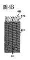
另外,圖4A和圖4B示出在本實施例模式中可以在同一基板上形成的佈線的端子部的截面結構。圖4A相當於沿圖4B中的線C1-C2的截面圖。In addition, FIGS. 4A and 4B show the cross-sectional structure of the terminal portion of the wiring that can be formed on the same substrate in this embodiment mode. Fig. 4A corresponds to a cross-sectional view taken along the line C1-C2 in Fig. 4B.
在圖4A中,形成在絕緣層486和閘極絕緣層492的疊層上的導電層437是用作輸入端子的用於連接的端子電極。另外,在圖4A中,在端子部中,使用與電極層479d、479e、479f、479g、479h相同的材料形成的電極層479i隔著第一絕緣層487a及第三絕緣層487b重疊於電連接到第一源極電極層485b的第一端子電極層439的下方。電極層479i不電連接到第一端子電極層439,藉由將電極層479i設定為與第一端子電極層439不同的電位,例如浮動、GND、0V等,可以形成用於對雜波的措施的電容或用於對靜電的措施的電容。另外,在第一端子電極層439上設置有第二端子電極層489,並且第一端子電極層439還隔著絕緣層486和閘極絕緣層492電連接到導電層437。In FIG. 4A, the
另外,可以使用與第一源極電極層485b相同的材料和相同的製程形成第一端子電極層439。可以使用與第二源極電極層488b相同的材料和相同的製程形成第二端子電極層489。另外,可以使用與第一閘極電極層481相同的材料和相同的製程形成導電層437。In addition, the first
本實施例模式可以與實施例模式1自由地組合。This embodiment mode can be freely combined with
實施例模式3Example Mode 3
在本實施例模式中,示出使用實施例模式2所示的EDMOS電路製造CPU(中央處理器)的例子。In this embodiment mode, an example of manufacturing a CPU (central processing unit) using the EDMOS circuit shown in embodiment mode 2 is shown.
圖5示出CPU的方塊圖的一個例子。圖5所示的CPU1001包括時序控制電路1002、指令解碼器1003、暫存器陣列1004、位址邏輯緩衝電路1005、資料匯流排介面1006、ALU(算術邏輯單元)1007、指令暫存器1008等。Fig. 5 shows an example of a block diagram of the CPU. The
上述電路使用實施例模式1或實施例模式2所示的薄膜電晶體、反相器電路、電阻、電容等製造。因為實施例模式1或實施例模式2所示的薄膜電晶體使用氫濃度被充分地降低了的氧化物半導體層,所以薄膜電晶體的截止電流可以為極小的值。因此,藉由使用具有氫濃度被充分地降低了的氧化物半導體層的薄膜電晶體而構成CPU1001的至少一部分,可以實現低耗電量。The above-mentioned circuit is manufactured using the thin film transistor, inverter circuit, resistor, capacitor, etc. shown in
在此,簡單地說明各電路。時序控制電路1002接受來自外部的指令,將其轉換為用於內部的資訊,並將其送到另外的組。另外,時序控制電路1002對應內部的工作而向外部供應儲存資料的讀入、寫入等的指令。指令解碼器1003具有將外部的指令轉換為用於內部的指令的功能。暫存器陣列1004是暫時儲存資料的揮發性記憶體。位址邏輯緩衝電路1005是指定外部記憶體的位址的電路。資料匯流排介面1006是將資料登錄到外部記憶體或印表機等的設備或者接收從外部記憶體或印表機等的設備輸出的資料的電路。ALU1007是進行運算的電路。指令暫存器1008是暫時記錄指令的電路。藉由上述電路的組合構成CPU。Here, each circuit is briefly described. The
藉由將實施例模式1或實施例模式2所示的薄膜電晶體用於CPU1001的至少一部分來降低待機時的漏電流,可以實現用於電子設備的驅動電路等的低耗電量化。By using the thin film transistor shown in
本實施例模式可以與實施例模式1或實施例模式2自由地組合。This embodiment mode can be independent of
實施例模式4Embodiment Mode 4
在本實施例模式中,說明上述實施例模式所示的半導體裝置的使用方式的一個例子。明確地說,參照附圖以下說明能夠以非接觸的方式進行資料的輸入/輸出的半導體裝置的應用例子。能夠以非接觸的方式進行資料的輸入/輸出的半導體裝置根據利用方式而也被稱為RFID標籤、ID標籤、IC標籤、RF標籤、無線標籤、電子標籤或無線晶片。In this embodiment mode, an example of the use of the semiconductor device shown in the above embodiment mode will be described. Specifically, an application example of a semiconductor device capable of data input/output in a non-contact manner will be described below with reference to the drawings. Semiconductor devices that can input/output data in a non-contact manner are also called RFID tags, ID tags, IC tags, RF tags, wireless tags, electronic tags, or wireless chips depending on their usage.
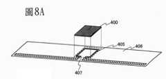
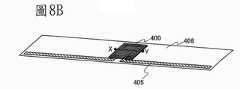
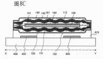
參照圖8A說明本實施例模式所示的半導體裝置的頂面結構的一個例子。圖8A所示的半導體裝置包括:設置有天線(也寫為片上天線(on-chip antenna))的半導體積體電路晶片400;以及設置有天線405(也寫為增益天線(booster antenna))的基底基板406。半導體積體電路晶片400設置在形成於基底基板406及天線405上的絕緣層410(圖8C)上。可以利用絕緣層410來將半導體積體電路晶片400固定在基底基板406以及天線405上。An example of the top surface structure of the semiconductor device shown in this embodiment mode will be described with reference to FIG. 8A. The semiconductor device shown in FIG. 8A includes: a semiconductor integrated
另外,為了防止因靜電放電而導致的靜電破壞(電路的錯誤工作或半導體元件的損傷)而在半導體積體電路晶片400表面上設置有導電遮罩體,當導電遮罩體的電阻高而不使天線405的圖案之間處於導通狀態時,也可以彼此接觸地設置天線405和設置在半導體積體電路晶片400表面上的導電遮罩體。In addition, in order to prevent electrostatic destruction (erroneous operation of the circuit or damage to semiconductor elements) caused by electrostatic discharge, a conductive mask is provided on the surface of the semiconductor integrated
在設置於半導體積體電路晶片400內的半導體積體電路中設置構成儲存部或邏輯部的多個薄膜電晶體等的元件。作為構成儲存部或邏輯部的薄膜電晶體,使用如下薄膜電晶體,即使用氫濃度被充分地降低而被高純度化的氧化物半導體層形成的薄膜電晶體。在根據本實施例模式的半導體裝置中,作為半導體元件除了可以應用場效應電晶體以外,還可以應用使用半導體層形成的記憶元件等。因此,可以製造並提供滿足很多用途的半導體裝置。In the semiconductor integrated circuit provided in the semiconductor integrated
圖7A示出圖8A所示的半導體積體電路晶片400所包括的天線和半導體積體電路的擴大圖。在圖7A中,天線101是轉數是1的矩形的環形天線,但是不侷限於該結構。環形天線的形狀不侷限於具有矩形的形狀,而也可以是具有曲線的形狀,例如也可以具有圓形。並且,轉數不侷限於1,也可以是複數。但是,當天線101的轉數是1時,可以降低產生在半導體積體電路100和天線101之間的寄生電容。FIG. 7A shows an enlarged view of an antenna and a semiconductor integrated circuit included in the semiconductor integrated
此外,在圖8A、圖7A中,以圍繞半導體積體電路100的周圍的方式配置天線101。在除了相當於虛線所示的饋電點(power feeding point)408的部分以外的區域中,天線101配置在與半導體積體電路100不同的區域中。另外,本發明不限於該結構,而如圖7B所示,也可以在除了相當於虛線所示的饋電點408的部分以外的區域中,以至少其一部分重疊於半導體積體電路100的方式配置天線101。但是,如圖8A、圖7A所示,藉由將天線101配置在與半導體積體電路100不同的區域中,可以降低產生在半導體積體電路100和天線101之間的寄生電容。In addition, in FIGS. 8A and 7A, the
在圖8A中,天線405主要在虛線407所圍繞的環形的部分中可以利用電磁感應而與天線101進行信號的授受或者電力的供應。此外,天線405主要在虛線407所圍繞的部分以外的區域中可以利用電波與詢問器進行信號的授受或者電力的供應。在詢問器和半導體裝置之間,用作載子(載波)的電波的頻率最好為30MHz以上且5GHz以下左右,例如使用950MHz、2.45GHz等的頻帶,即可。In FIG. 8A, the
此外,雖然在虛線407所圍繞部分中,天線405是轉數是1的矩形的環狀,但是在本發明不侷限於該結構。環狀部分不侷限於具有矩形,而也可以是具有曲線的形狀,例如可以具有圓形。此外,轉數不侷限於1,而也可以是複數。In addition, although the
本實施例模式所示的半導體裝置也可以應用電磁感應方式、電磁耦合方式、微波方式。在採用微波方式的情況下,根據所使用的電磁波的波長適當地決定天線101、天線405的形狀即可。The semiconductor device shown in this embodiment mode can also apply an electromagnetic induction method, an electromagnetic coupling method, and a microwave method. In the case of adopting the microwave method, the shape of the
例如,在應用微波方式(例如,UHF頻帶(860MHz頻帶到960MHz頻帶)、2.45GHz頻帶等)作為半導體裝置的信號傳輸方式的情況下,根據用於信號傳輸的電磁波的波長來適當地設定天線的長度或形狀等即可。例如,可以將天線形成為線形(例如,偶極天線)、平坦的形狀(例如,貼片天線或帶形)等。此外,天線的形狀不限於直線形,也可以根據電磁波的波長以曲線狀、蜿蜒形狀或者組合這些而成的形狀而設置。For example, in the case of applying a microwave method (e.g., UHF band (860MHz band to 960MHz band), 2.45GHz band, etc.) as the signal transmission method of the semiconductor device, the antenna’s power is appropriately set according to the wavelength of the electromagnetic wave used for signal transmission. The length or shape is sufficient. For example, the antenna can be formed into a linear (e.g., dipole antenna), flat shape(For example, patch antenna or ribbon) and so on. In addition, the shape of the antenna is not limited to a linear shape, and may be arranged in a curved shape, a serpentine shape, or a combination of these according to the wavelength of the electromagnetic wave.
圖9示出以線圈狀設置天線101、天線405,並應用電磁感應方式或電磁耦合方式的例子。FIG. 9 shows an example in which the
在圖9中,在設置有作為增益天線的線圈狀天線405的基底基板406上提供設置有線圈狀天線101的半導體積體電路晶片400。另外,用作增益天線的天線405隔著基底基板406形成有電容。In FIG. 9, a semiconductor integrated
接著,說明半導體積體電路晶片400和增益天線的結構及其配置。圖8B相當於一種半導體裝置的立體圖,其中層疊有圖8A所示的半導體積體電路晶片400和形成在基底基板406上的天線405。另外,圖8C相當於沿著圖8B的虛線X-Y的截面圖。Next, the structure and arrangement of the semiconductor integrated
圖8C所示的半導體積體電路晶片400可以使用實施例模式1或實施例模式2所示的半導體裝置,在此,將被分割成每一個的晶片稱為半導體積體電路晶片。另外,雖然圖8C所示的半導體積體電路晶片是使用實施例模式1的例子,但是不侷限於該結構,也可以使用其他實施例模式。The semiconductor integrated
圖8C所示的半導體積體電路100由第一絕緣體112、第二絕緣體102夾持,並且其側面也被密封。在本實施例模式中,在以夾持多個半導體積體電路的方式貼合第一絕緣體、第二絕緣體之後,將其分割為每一個半導體積體電路的疊層體。在被分割的疊層體上形成導電遮罩體,以製造半導體積體電路晶片400。分割方法只要能夠物理性地分割就沒有特別的限制。在本實施例模式中藉由照射雷射來進行分割。The semiconductor integrated
雖然在圖8C中半導體積體電路100配置在比天線101更靠近天線405的位置,但是不侷限於該結構。也可以將天線101配置在比半導體積體電路100更接近天線405的位置。另外,半導體積體電路100和天線101可以直接黏著到第一絕緣體112、第二絕緣體102,也可以利用用作黏合劑的黏合層而黏著到第一絕緣體112、第二絕緣體102。Although the semiconductor integrated
接著,說明根據本實施例模式的半導體裝置的工作。圖6是示出根據本實施例模式的半導體裝置的結構的方塊圖的一個例子。圖6所示的半導體裝置420包括用作增益天線的天線422、半導體積體電路423、片上天線(on-chip antenna)424。當電磁波從詢問器421發出時,天線422接收該電磁波,因此,在天線422內產生交流電流,且在天線422周圍產生磁場。然後,天線422所具有的環狀部分和具有環形形狀的天線424相互電磁耦合,使得天線424中產生感應電動勢。半導體積體電路423藉由利用上述感應電動勢接收來自詢問器421的信號或電力。反之,藉由依照半導體積體電路423中產生的信號使電流流過天線424使得天線422中產生感應電動勢,藉由將該感應電動勢作為從詢問器421發出的電波的反射波傳送,可以將信號發送到詢問器421。Next, the operation of the semiconductor device according to this embodiment mode will be explained. FIG. 6 is an example of a block diagram showing the structure of a semiconductor device according to this embodiment mode. The
另外,天線422可以分為主要進行和天線424之間的電磁耦合的環狀部分和主要接收來自詢問器421的電波的部分。主要接收來自詢問器421的電波的部分中的天線422只要具有可以接收電波的形狀即可。例如,採用偶極天線、折疊偶極天線、槽縫天線、彎折線天線、微帶天線等的形狀即可。In addition, the
雖然圖8A至圖8C說明包括只有一個天線的半導體積體電路的結構,但是本發明不限於該結構。半導體積體電路還可以包括兩個天線,即用來接收電力的天線和用來接收信號的天線。藉由具有兩個天線,可以分別使用用於供電的電波的頻率和用來發送信號的電波的頻率。Although FIGS. 8A to 8C illustrate the structure including a semiconductor integrated circuit having only one antenna, the present invention is not limited to this structure. The semiconductor integrated circuit may also include two antennas, namely an antenna for receiving power and an antenna for receiving signals. By having two antennas, the frequency of the electric wave used for power supply and the frequency of the electric wave used for signal transmission can be used separately.
在根據本實施例模式的半導體裝置中,使用片上天線,並且可以在增益天線與片上天線之間以非接觸的方式進行信號或電力的發送和接收。因此,與將外部天線連接到半導體積體電路的情況不同,半導體積體電路與天線之間的連接不容易被外力切斷,而可以抑制該連接的初期故障的產生。此外,由於在本實施例模式中使用增益天線,所以與只使用片上天線的情況不同,片上天線的尺寸或形狀較少受到半導體積體電路的面積的限制。因此,天線能接收的電波的頻帶不受到限制,而且可以享受外部天線所具有的優點,該優點是能夠增大通信距離。In the semiconductor device according to this embodiment mode, an on-chip antenna is used, and transmission and reception of signals or power can be performed in a non-contact manner between the booster antenna and the on-chip antenna. Therefore, unlike the case where the external antenna is connected to the semiconductor integrated circuit, the connection between the semiconductor integrated circuit and the antenna is not easily cut off by external force, and the occurrence of initial failure of the connection can be suppressed. In addition, since the booster antenna is used in this embodiment mode, unlike the case where only the on-chip antenna is used, the size or shape of the on-chip antenna is less limited by the area of the semiconductor integrated circuit. Therefore, the frequency band of the radio waves that the antenna can receive is not limited, and the advantages of the external antenna can be enjoyed, which is that the communication distance can be increased.
半導體積體電路也可以直接形成在撓性基板上。另外,也可以將半導體積體電路從製造基板(例如,玻璃基板)轉置到另一基板(例如,塑膠基板)。The semiconductor integrated circuit can also be directly formed on the flexible substrate. In addition, semiconductor integrated circuits can also be manufactured from substrates (for example, glass-basedThe board) is transposed to another substrate (for example, a plastic substrate).
另外,當將半導體集成基板從製造基板轉置到另一基板時,沒有特別的限制而可以使用各種各樣的方法。例如,在製造基板和半導體積體電路之間形成分離層,即可。In addition, when the semiconductor integrated substrate is transferred from a manufacturing substrate to another substrate, there is no particular limitation and various methods can be used. For example, a separation layer may be formed between the manufacturing substrate and the semiconductor integrated circuit.
例如,當形成金屬氧化膜作為分離層時,可以利用晶化而將該金屬氧化膜脆弱化,而從製造基板剝離包括作為被分離層的半導體積體電路的元件層。另外,也可以在藉由晶化而將該金屬氧化膜脆弱化之後,利用溶液或NF3、BrF3、ClF3等的氟化鹵氣體進一步進行蝕刻來去除分離層的一部分,並且在被脆弱化了的金屬氧化膜中進行剝離。For example, when a metal oxide film is formed as a separation layer, the metal oxide film can be weakened by crystallization, and the element layer including the semiconductor integrated circuit as the separated layer can be peeled from the manufacturing substrate. In addition, after the metal oxide film is fragile by crystallization, the metal oxide film can be further etched with a solution or a halogen fluoride gas such as NF3, BrF3, ClF3, etc. to remove a part of the separation layer. The metal oxide film is peeled off.
另外,當將包含氮、氧或氫等的膜(例如,包含氫的非晶矽膜、包含氫的合金膜、包含氧的合金膜等)用於分離層並將透光基板用於製造基板時,可以從製造基板一側對分離層照射雷射,使包含在玻璃層內的氮、氧或氫汽化,而在製造基板和分離層之間進行剝離。In addition, when a film containing nitrogen, oxygen, hydrogen, etc. (for example, an amorphous silicon film containing hydrogen, an alloy film containing hydrogen, an alloy film containing oxygen, etc.) is used for the separation layer and the light-transmitting substrate is used for manufacturing the substrate In this case, the separation layer can be irradiated with a laser from the side where the substrate is manufactured to vaporize the nitrogen, oxygen, or hydrogen contained in the glass layer, and peel off between the substrate and the separation layer.
另外,也可以藉由蝕刻去除分離層來從製造基板剝離被分離層。In addition, the separation layer may be removed by etching to peel the separation layer from the manufacturing substrate.
另外,也可以使用對製造基板機械地進行研磨並去除的方法、對製造基板進行利用NF3、BrF3、ClF3等的氟化鹵氣體或HF的蝕刻並去除的方法等。此時,也可以不使用分離層。In addition, a method of mechanically grinding and removing the manufactured substrate, a method of etching and removing the manufactured substrate using halogen fluoride gas such as NF3, BrF3, ClF3, or HF, or the like may also be used. In this case, the separation layer may not be used.
另外,也可以利用雷射照射、使用氣體或溶液等的蝕刻或者銳利的刀具、解剖刀來形成使分離層露出的槽,並且以該槽為起點而從製造基板的分離層剝離被分離層。In addition, laser irradiation, gas or solution, etc. can also be used.A cut or sharp knife or scalpel is used to form a groove exposing the separation layer, and the separation layer is peeled from the separation layer of the manufacturing substrate using the groove as a starting point.
作為剝離方法,例如施加機械力(使用人的手或鉗子來剝離的處理或使滾子轉動來進行分離的處理等),即可。另外,也可以使液體滴落到槽中來使液體深入與分離層的介面,而從分離層剝離被分離層。另外,也可以將NF3、BrF3、ClF3等的氟化氣體引入到槽中,利用氟化氣體對分離層進行蝕刻並去除,而從製造基板剝離被分離層。另外,也可以當進行剝離時,澆水等的液體並進行剝離。As a peeling method, for example, mechanical force (a process of peeling using a human hand or pliers, a process of rotating a roller to perform separation, etc.) may be applied. In addition, the liquid may be dropped into the groove so that the liquid penetrates into the interface with the separation layer, and the separated layer is peeled from the separation layer. In addition, fluorinated gas such as NF3, BrF3, ClF3, etc. may be introduced into the groove, and the separation layer may be etched and removed with the fluorinated gas, and the separated layer may be peeled from the manufacturing substrate. In addition, when peeling is performed, a liquid such as water may be watered to perform peeling.
作為另一剝離方法,當使用鎢形成分離層時,可以使用氨水和過氧化氫水的混合溶液對分離層進行蝕刻並剝離。As another peeling method, when tungsten is used to form the separation layer, a mixed solution of ammonia water and hydrogen peroxide water may be used to etch and peel the separation layer.
在使用氫濃度被充分地降低而被高純度化的氧化物半導體層的薄膜電晶體中,截止電流小而可以實現低耗電量。另外,藉由覆蓋半導體積體電路的導電遮罩體,可以防止靜電放電造成的半導體積體電路的靜電損壞(電路的錯誤工作或半導體元件的損壞)。並且,可以提供具有耐性的可靠性高的半導體裝置,其中利用夾持半導體積體電路的一對絕緣體而實現薄型化及小型化。In a thin film transistor using an oxide semiconductor layer whose hydrogen concentration is sufficiently reduced to be highly purified, the off-current is small and low power consumption can be achieved. In addition, the conductive shield covering the semiconductor integrated circuit can prevent electrostatic damage to the semiconductor integrated circuit (wrong operation of the circuit or damage to the semiconductor element) caused by electrostatic discharge. In addition, it is possible to provide a durable and highly reliable semiconductor device in which a pair of insulators sandwiching a semiconductor integrated circuit are used to achieve thinning and downsizing.
實施例模式5Embodiment Mode 5
在本實施例模式中,以下參照附圖說明使用上述實施例模式4的裝置形成的可以以非接觸的方式進行資料輸入/輸出的半導體裝置的應用例子。以非接觸的方式進行資料輸入/輸出的半導體裝置根據利用方式還被稱為RFID標籤、ID標籤、IC標籤、IC晶片、RF標籤、無線標籤、電子標籤或無線晶片。In this embodiment mode, the following description will be made with reference to the drawings, which can be used to input data in a non-contact manner using the device of the above embodiment mode 4./ Output application examples of semiconductor devices. Semiconductor devices that perform data input/output in a non-contact manner are also called RFID tags, ID tags, IC tags, IC chips, RF tags, wireless tags, electronic tags, or wireless chips depending on the usage mode.
半導體裝置800具有以非接觸的方式進行資料收發的功能,並且包括高頻電路810、電源電路820、重設電路830、時鐘產生電路840、資料解調變電路850、資料調變電路860、控制其他電路的控制電路870、儲存電路880、以及天線890(參照圖10A)。高頻電路810是接收來自天線890的信號並且將由資料調變電路860接收的信號從天線890輸出的電路。電源電路820是根據接收信號產生電源電位的電路。重設電路830是產生重設信號的電路。時鐘產生電路840是根據從天線890接收的接收信號產生各種時鐘信號的電路。資料解調變電路850是解調接收信號且將該信號輸出到控制電路870的電路。資料調變電路860是調變從控制電路870接收的信號的電路。此外,作為控制電路870,例如設置有取碼電路910、判碼電路920、CRC判定電路930以及輸出器電路940。另外,取碼電路910是將傳送到控制電路870的指令所包括的多個碼分別抽出的電路。判碼電路920是比較被抽出的碼與相當於參考值的碼而判定指令內容的電路。CRC判定電路930是根據被判定的碼檢測出是否存在發送錯誤等的電路。The
接著,對上述半導體裝置的工作的一個例子進行說明。首先,天線890接收無線信號。無線信號經由高頻電路810而被傳送到電源電路820,並且在電源電路820中產生高電源電位(以下,表示為VDD)。VDD提供給半導體裝置800所具有的各個電路。此外,經由高頻電路810被傳送到資料解調變電路850的信號被解調(以下,解調信號)。而且,經由高頻電路810並且經過重設電路830及時鐘產生電路840的信號以及解調信號被傳送到控制電路870。取碼電路910、判碼電路920以及CRC判定電路930等分析被傳送到控制電路870的信號。然後,根據被分析的信號,輸出儲存在儲存電路880內的半導體裝置的資訊。被輸出的半導體裝置的資訊經過輸出器電路940而被編碼。再者,被編碼的半導體裝置800的資訊經過資料調變電路860,由天線890作為無線信號發送。另外,在構成半導體裝置800的多個電路中,低電源電位(以下,VSS)是共同的,可以將VSS作為GND來使用。Next, an example of the operation of the above-mentioned semiconductor device will be describedBright. First, the
如此,藉由將信號從通信裝置傳送到半導體裝置800並且使用通信裝置接收從該半導體裝置800傳送來的信號,可以讀出半導體裝置的資料。In this way, by transmitting a signal from the communication device to the
此外,半導體裝置800既可以是不安裝電源(電池)而由電磁波將電源電壓供應給各個電路的樣式,又可以是安裝電源(電池)並且由電磁波和電源(電池)將電源電壓供應給各個電路的樣式。In addition, the
接下來,說明可以以非接觸的方式進行資料輸入/輸出的半導體裝置的使用方式的一個例子。包括顯示部3210的可攜式終端的側面設置有通信裝置3200,並且產品3220的側面設置有半導體裝置3230(圖10B)。當將通信裝置3200接近於產品3220所包括的半導體裝置3230時,有關商品的資訊諸如產品的原材料、原產地、各個生產過程的檢查結果、流通過程的歷史等以及產品說明等被顯示在顯示部3210上。此外,當使用傳送帶搬運商品3260時,可以利用通信裝置3240和設置在商品3260上的半導體裝置3250,對該商品3260進行檢查(圖10C)。如此,藉由將半導體裝置利用於系統,可以容易獲得資訊而實現高功能化和高附加價值化。Next, explain that data can be input/input in a non-contact mannerAn example of how the semiconductor device is used. The side of the portable terminal including the
如上所述,半導體裝置的應用範圍極為廣泛,可以應用到廣泛領域的電子設備。As described above, the application range of semiconductor devices is extremely wide and can be applied to electronic equipment in a wide range of fields.
實施例模式6Embodiment Mode 6
根據實施例模式1或實施例模式2得到的薄膜電晶體是使用被高純度化的氧化物半導體形成的薄膜電晶體,並且藉由利用該薄膜電晶體構成電路,可以實現低耗電量並將儲存電路的工作穩定化。The thin film transistor obtained according to
在本實施例模式中,示出可以使用實施例模式1的薄膜電晶體構成的儲存電路的一個例子。In this embodiment mode, an example of a storage circuit that can be constructed using the thin film transistor of
圖11A示出儲存電路的一個例子的等效電路圖。圖11A所示的儲存電路包括列解碼器、寫入電路及更新電路、行解碼器、配置為矩陣狀的記憶元件1100。連接到配置為矩陣狀的記憶元件1100的信號線藉由寫入電路及更新電路連接到列解碼器。連接到配置為矩陣狀的記憶元件1100的掃描線連接到行解碼器。對列解碼器輸入位元信號。對寫入電路及更新電路輸入讀使能信號/寫使能信號(RE/WE)、資料信號(data)和輸出信號(OUT)。FIG. 11A shows an equivalent circuit diagram of an example of the storage circuit. The storage circuit shown in FIG. 11A includes a column decoder, a write circuit and an update circuit, a row decoder, and
各記憶元件1100包括電容元件和薄膜電晶體,該薄膜電晶體的源極電極和汲極電極中的一方連接到信號線,該薄膜電晶體的源極電極和汲極電極中的另一方連接到電容元件的一方的電極,該電容元件的另一方的電極連接到低電位一側(最好是參考電位Vss)。Each
圖11B示出設置在圖11A所示的寫入電路及更新電路的更新電路的具體的一個結構例子。FIG. 11B shows a specific configuration example of the refresh circuit provided in the write circuit and refresh circuit shown in FIG. 11A.
圖11B所示的寫入電路及更新電路包括且電路(AND電路)和讀出放大器。對第一且電路1101、第二且電路1102以及第三且電路1103的一方的輸入輸入來自列解碼器的信號。對第一且電路1101的另一方的輸入輸入PRC信號,對第二且電路1102的另一方的輸入輸入寫使能信號(WE),對第三且電路1103的另一方的輸入輸入讀使能信號(RE)。第一且電路1101的輸出控制第一開關1104的導通/截止,第二且電路1102的輸出控制第二開關1105的導通/截止,並且第三且電路1103的輸出控制第三開關1106的導通/截止。預充電信號線Vprc藉由第一開關1104連接到信號線,資料信號線data藉由第二開關1105連接到信號線。The write circuit and update circuit shown in FIG. 11B include an AND circuit (AND circuit) and a sense amplifier. A signal from the column decoder is input to the input of one of the first sub-circuit 1101, the second sub-circuit 1102, and the third sub-circuit 1103. The PRC signal is input to the input of the other side of the
藉由第一開關1104以及第二開關1105連接的信號線藉由第三開關1106連接到讀出放大器。信號從該讀出放大器輸出到輸出信號線(OUT)。The signal line connected through the
另外,作為上述且電路使用具有一般的結構的且電路即可,最好採用簡單的結構。In addition, as the above-mentioned circuit, a circuit having a general structure may be used, and a simple structure is preferable.
注意,讀出放大器是指具有將被輸入的信號放大的功能的電路。Note that the sense amplifier refers to a circuit that has a function of amplifying the input signal.
在此,作為信號,可以使用例如利用電壓、電流、電阻或頻率等的模擬信號或數位信號。例如,藉由作為電位至少設定第一電位和第二電位,作為第一電位使用高位準(高電位,也稱為VH)的電位,而作為第二電位使用低位準(低電位,也稱為VL)的電位,可以設定二值的數位信號。另外,VH和VL最好是一定的值。但是,也可以考慮到雜波的影響而將VH和VL設定為在一定範圍內的數值,而不是一定的值。Here, as the signal, for example, an analog signal or a digital signal using voltage, current, resistance, frequency, or the like can be used. For example, by setting at least a first potential and a second potential as potentials, a high level (high potential, also called VH ) potential is used as the first potential, and a low level (low potential, also called VH ) is used as the second potential. For the potential of VL ), a binary digital signal can be set. In addition, VH and VL are preferably constant values. However, it is also possible to consider the influence of clutter and set VH and VL to values within a certain range instead of a certain value.
另外,在此,附上“第一”、“第二”等的序數的用語用來避免每個要素的混同,而不用來限定數目。In addition, here, the terms attaching ordinal numbers such as "first" and "second" are used to avoid the confusion of each element, and are not used to limit the number.
如上所述,可以使用實施例模式1所說明的薄膜電晶體並實施例模式2所說明的電容來製造儲存電路。As described above, the thin film transistor described in
在設計步驟根據預先被評價的記憶元件1100的漏電流已經決定了以一定的時間間隔作為儲存電路的更新時序。換言之,考慮到完成晶片之後的漏電流的溫度依賴性、製造方法的變動而決定儲存電路的更新時序。In the design step, a certain time interval has been determined as the update sequence of the storage circuit according to the leakage current of the
因為實施例模式1或實施例模式2所示的薄膜電晶體使用氫濃度被充分地降低了的氧化物半導體層,所以薄膜電晶體的截止電流可以是極小的值,從-30℃至120℃的截止電流的溫度特性也幾乎沒有變化,因此可以維持極小的值。Because the thin film transistor shown in
因此,藉由使用實施例模式1或實施例模式2所示的薄膜電晶體,可以將更新時序與使用矽形成的電晶體相比設定為長的時間間隔,從而可以縮減待機時的耗電量。Therefore, by using the thin film transistors shown in
另外,因為本實施例模式的儲存電路幾乎沒有截止電流的溫度依賴性,所以本實施例模式的儲存電路適於車載的電子設備。待機時的漏電流極小。在電動汽車中,即使待機時間長,每一定充電量的行車距離也幾乎沒有變化。In addition, since the storage circuit of this embodiment mode has almost no temperature dependence of the off current, the storage circuit of this embodiment mode is suitable for vehicle-mounted electronic equipment. The leakage current during standby is extremely small. In electric vehicles, even if the standby time is long, the driving distance per a certain amount of charge hardly changes.
在實施例模式1或實施例模式2所示的電晶體中,去除有可能在氧化物半導體中成為載子的給體(施體或受體)的雜質來使該雜質極少,而使用本徵或實際上本徵的半導體。In the transistor shown in
圖12是示出實施例模式1或實施例模式2所示的電晶體的源極電極-汲極電極間帶結構的圖。在理想狀態下,實現高純度化的氧化物半導體的費米能級位於禁止帶中央。在氫濃度被充分地降低的氧化物半導體中,沒有少數載子(此時的電洞)或幾乎沒有少數載子(此時的電洞)。FIG. 12 is a diagram showing the structure of the band between the source electrode and the drain electrode of the transistor shown in
在功函數是Φm且氧化物半導體的電子親和力是χ的情況下,當功函數是Φm小於電子親和力是χ時,對電子形成歐姆接觸。In the case where the work function is Φm and the electron affinity of the oxide semiconductor is χ, when the work function is Φm smaller than the electron affinity is χ, an ohmic contact is formed with electrons.
在此,當Φm=χ時,在接合面中電極金屬的費米能級和氧化物半導體的傳導帶端的能級一致。當假設:帶隙是3.05eV;電子親和力是4.3eV;且處於本徵狀態(載子密度是大約1×10⁻⁷/cm3),並作為源極電極和汲極電極使用功函數是4.3eV的鈦(Ti)時,如圖12所示那樣對電子不形成勢壘。Here, when Φm=χ, the Fermi level of the electrode metal in the joint surface coincides with the energy level of the conduction band end of the oxide semiconductor. When assuming: the band gap is 3.05eV; the electron affinity is 4.3eV; and it is in the intrinsic state (the carrier density is about 1×10⁻⁷ /cm3 ), and the work function used as the source electrode and drain electrode is 4.3 In the case of eV titanium (Ti), as shown in FIG. 12, no barrier is formed against electrons.
圖13示出能帶結構的示意圖。在對汲極電極施加正的電壓(VD>0)的情況下,虛線示出對閘極不施加電壓的情況(VG=0),而實線示出對閘極施加正的電壓的情況(VG>0)。當對閘極不施加電壓時,因勢壘高而載子(電子)不從電極植入到氧化物半導體一側,而示出不使電流流過的截止狀態。另一方面,當對閘極施加正的電壓時,勢壘降低,而示出使電流流過的導通狀態。Fig. 13 shows a schematic diagram of an energy band structure. When a positive voltage is applied to the drain electrode (VD>0), the broken line shows the case where no voltage is applied to the gate (VG=0), and the solid line shows the case where a positive voltage is applied to the gate ( VG>0). When no voltage is applied to the gate electrode, since the potential barrier is high, carriers (electrons) are not implanted from the electrode to the oxide semiconductor side, and an off state is shown in which no current flows. On the other hand, when a positive voltage is applied to the gate, the potential barrier is lowered, and an on-state in which current flows is shown.
在此,勢壘高度對載子的遷移率有影響。因此,當使汲極電壓高時,勢壘高度(hb)變小,且遷移率變大。如果源極電極的功函數的程度Φm大概與氧化物半導體的電子親和力相同,則hb進一步變小,且可以期待更高遷移率。但是,需要保證上述電極材料不與氧化物半導體接觸而形成絕緣物。Here, the barrier height has an influence on the mobility of carriers. Therefore, when the drain voltage is made high, the barrier height (hb) becomes smaller and the mobility becomes larger. If the degree of the work function Φm of the source electrode is approximately the same as the electron affinity of the oxide semiconductor, hb will be further reduced, and higher mobility can be expected. However, it is necessary to ensure that the above-mentioned electrode material does not contact the oxide semiconductor to form an insulator.
在上述情況下,在底閘型(反交錯型)電晶體中,源極電極-汲極電極之間的勢壘變小,而容易產生寄生通道。因此,為了得到更高的遷移率,最好採用頂閘型電晶體。In the above situation, in the bottom gate type (inverse staggered type) transistor, the potential barrier between the source electrode and the drain electrode becomes smaller, and parasitic channels are likely to occur. Therefore, in order to obtain higher mobility, it is best to use a top-gate transistor.
圖14A是使閘極電壓為正時的MOS結構的能帶圖,並示出使用氧化物半導體形成的電晶體中的能帶圖。此時,在被高純度化的氧化物半導體中幾乎沒有熱激發載子,並且即使進一步施加正的閘極電壓,在閘極絕緣膜近旁也不蓄積載子。但是,如圖13所示,從源極電極一側植入的載子也可以傳播。14A is an energy band diagram of the MOS structure when the gate voltage is positive,It also shows an energy band diagram in a transistor formed using an oxide semiconductor. At this time, there are almost no thermally excited carriers in the highly purified oxide semiconductor, and even if a positive gate voltage is further applied, no carriers are accumulated near the gate insulating film. However, as shown in FIG. 13, carriers implanted from the source electrode side can also propagate.
圖14B是使閘極電壓為負時的MOS結構的能帶圖,並示出使用氧化物半導體形成的電晶體中的能帶圖。因為在氧化物半導體中幾乎沒有少數載子(電洞),所以在閘極絕緣膜近旁也不蓄積載子。上述情況意味著截止電流小。14B is an energy band diagram of the MOS structure when the gate voltage is made negative, and shows an energy band diagram in a transistor formed using an oxide semiconductor. Since there are almost no minority carriers (holes) in an oxide semiconductor, no carriers are accumulated near the gate insulating film. The above situation means that the off current is small.
另外,圖15示出使用矽半導體形成的電晶體的能帶圖。矽半導體的本徵載子密度是1.45×10¹⁰/cm3(300K)左右,且在室溫中也有載子。因為在實際上使用添加有磷或硼等的雜質的矽晶圓,所以在實際上在矽半導體內有1×1014/cm3以上的載子,這有助於源極電極-汲極電極間的傳導。並且,因為矽半導體的帶隙是1.12eV,所以使用矽半導體形成電晶體根據溫度截止電流的變動較大。In addition, FIG. 15 shows an energy band diagram of a transistor formed using a silicon semiconductor. The intrinsic carrier density of silicon semiconductors is about 1.45×10¹⁰ /cm3 (300K), and there are carriers at room temperature. Since silicon wafers containing impurities such as phosphorus and boron are actually used, there are actually more than 1×10¹⁴ /cm3 carriers in the silicon semiconductor, which contributes to the source electrode-drain electrode Between conduction. In addition, since the band gap of a silicon semiconductor is 1.12 eV, a silicon semiconductor is used to form a transistor, and the cutoff current varies greatly depending on the temperature.
如上所述,不將帶隙寬的氧化物半導體用於電晶體,而盡可能地降低形成施體的氫等的雜質,使載子濃度為1×10¹⁴/cm3以下,最好為1×1012/cm3以下。由此,可以去除在實用上的工作溫度下被熱激發的載子,並僅使用從源極電極一側植入的載子來使電晶體工作。由此,可以將截止電流降低到低於1×10-13A以下,並且得到即使溫度變化截止電流也幾乎沒有變化的極穩定地工作的電晶體。As mentioned above, instead of using an oxide semiconductor with a wide band gap for the transistor, the donor-forming hydrogen and other impurities are reduced as much as possible, and the carrier concentration is 1×10¹⁴ /cm3 or less, preferably 1 ×10¹² /cm3 or less. As a result, carriers that are thermally excited at a practical operating temperature can be removed, and only the carriers implanted from the source electrode side can be used to operate the transistor. As a result, it is possible to reduce the off current to less than 1×10-13 A or less, and to obtain an extremely stable operating transistor with almost no change in off current even with temperature changes.
實施例模式7
在本實施例模式中,示出可以使用實施例模式1或實施例模式2所示的薄膜電晶體來構成的移位暫存器的一個例子。In this embodiment mode, an example of a shift register that can be constructed using the thin film transistor shown in
圖16A示出移位暫存器的一個例子的等效電路圖。圖16A所示的移位暫存器包括兩個時鐘信號線、電連接到這些時鐘信號線中的任一個的兩級正反器。另外,可以設置更多的時鐘信號線,並且可以設置更多級的正反器。Fig. 16A shows an equivalent circuit diagram of an example of a shift register. The shift register shown in FIG. 16A includes two clock signal lines and a two-stage flip-flop electrically connected to any one of these clock signal lines. In addition, more clock signal lines can be set, and more stages of flip-flops can be set.
時鐘信號分別輸入到兩個時鐘信號線,當一方的時鐘信號線轉換為高位準(VH)時,另一方的時鐘信號線轉換為低位準(VL),而進行工作。The clock signals are respectively input to two clock signal lines, and when one of the clock signal lines is converted to a high level (VH ), the other clock signal line is converted to a low level (VL ) to perform work.
圖16A說明移位暫存器,其中依次包括:電連接到第一時鐘信號線CLK的第一級正反器;電連接到第二時鐘信號線CLKB的第二級正反器;第n-1級的正反器;以及第n級的正反器。但是,不侷限於該結構,而至少具有第一正反器和第二正反器即可。16A illustrates the shift register, which in turn includes: a first-stage flip-flop electrically connected to the first clock signal line CLK; a second-stage flip-flop electrically connected to the second clock signal line CLKB;
時鐘信號線CLK是被輸入時鐘信號CK的佈線。The clock signal line CLK is a wiring to which the clock signal CK is input.
時鐘信號線CLKB是被輸入時鐘信號CKB的佈線。The clock signal line CLKB is a wiring to which the clock signal CKB is input.
例如,可以使用非電路(反相器電路)分別產生時鐘信號CK和時鐘信號CKB。For example, a non-circuit (inverter circuit) may be used to generate the clock signal CK and the clock signal CKB, respectively.
對第一正反器輸入啟動信號SP和啟動信號SPB,輸入用作時鐘信號的時鐘信號CK,並且根據所輸入的信號SP和信號SPB的信號狀態和時鐘信號CK的信號狀態而輸出輸出信號OUT。注意,在此,信號狀態例如是指信號的電位、電流或頻率等。The start signal SP and the start signal SPB are input to the first flip-flop, the clock signal CK used as a clock signal is input, and the signal state of the input signal SP and signal SPB and the signal state of the clock signal CK are changed.Output the output signal OUT. Note that here, the signal state refers to, for example, the potential, current, or frequency of the signal.
例如,可以使用非電路(反相器電路)分別產生啟動信號SP和啟動信號SPB。For example, a non-circuit (inverter circuit) may be used to generate the start signal SP and the start signal SPB, respectively.
在此,作為信號,可以使用例如利用電壓、電流、電阻或頻率等的類比信號或數位信號。例如,藉由作為電位至少設定第一電位和第二電位,作為第一電位使用高位準(高電位,也稱為VH)的電位,而作為第二電位使用低位準(低電位,也稱為VL)的電位,可以設定二值的數位信號。另外,VH和VL最好是一定的值。但是,也可以考慮到雜波的影響而將VH和VL設定為在一定範圍內的數值,而不是一定的值。Here, as the signal, for example, an analog signal or a digital signal using voltage, current, resistance, frequency, or the like can be used. For example, by setting at least a first potential and a second potential as potentials, a high level (high potential, also called VH) potential is used as the first potential, and a low level (low potential, also called VH) is used as the second potential. The potential of VL) can be set as a binary digital signal. In addition, VH and VL are preferably constant values. However, it is also possible to set VH and VL to values within a certain range instead of a certain value in consideration of the influence of clutter.
另外,在此,附上“第一”、“第二”等的序數的用語用來避免每個要素的混同,而不用來限定數目。In addition, here, the terms attaching ordinal numbers such as "first" and "second" are used to avoid the confusion of each element, and are not used to limit the number.
第二正反器具有如下功能,即被輸入作為啟動信號SP的第一正反器的輸出信號OUT,被輸入作為時鐘信號的時鐘信號CK2,並作為輸出信號輸出根據被輸入的輸出信號FF1out及時鐘信號CK2而設定狀態的信號FF2out的功能。The second flip-flop has the function of inputting the output signal OUT of the first flip-flop as the start signal SP, inputting the clock signal CK2 as the clock signal, and outputting as the output signal according to the inputted output signal FF1out and The clock signal CK2 sets the function of the signal FF2out.
對第二正反器輸入啟動信號SP和啟動信號SPB,輸入作為時鐘信號的時鐘信號CK2,並且第二正反器根據被輸入的信號SP及信號SPB的狀態和時鐘信號CK2的信號的狀態而輸出輸出信號OUTB。The start signal SP and the start signal SPB are input to the second flip-flop, and the clock signal CK2 as a clock signal is input, and the second flip-flop is changed according to the input signal SP and the state of the signal SPB and the signal state of the clock signal CK2 Output output signal OUTB.
圖16B示出圖16A所示的第一正反器的具體的一個結構例子。16B shows a specific one of the first flip-flop shown in FIG. 16AStructure example.
啟動信號SP輸入到第一薄膜電晶體1111的源極電極和汲極電極中的一方以及第四薄膜電晶體1114的源極電極和汲極電極中的一方。The start signal SP is input to one of the source electrode and the drain electrode of the first
啟動信號SPB輸入到第二薄膜電晶體1112的源極電極和汲極電極中的一方以及第三薄膜電晶體1113的源極電極和汲極電極中的一方。The start signal SPB is input to one of the source electrode and the drain electrode of the second
時鐘信號CLK輸入到第一薄膜電晶體1111、第二薄膜電晶體1112、第三薄膜電晶體1113以及第四薄膜電晶體1114的閘極。The clock signal CLK is input to the gates of the first
第一薄膜電晶體1111的源極電極和汲極電極中的另一方連接到第五薄膜電晶體1115的閘極和第一電容元件1119的一方的電極。The other of the source electrode and the drain electrode of the first
第二薄膜電晶體1112的源極電極和汲極電極中的另一方連接到第六薄膜電晶體1116的閘極和第二電容元件1120的一方的電極。The other of the source electrode and the drain electrode of the second
第三薄膜電晶體1113的源極電極和汲極電極中的另一方連接到第七薄膜電晶體1117的閘極和第三電容元件1121的一方的電極。The other of the source electrode and the drain electrode of the third
第四薄膜電晶體1114的源極電極和汲極電極中的另一方連接到第八薄膜電晶體1118的閘極和第四電容元件1122的一方的電極。The other of the source electrode and the drain electrode of the fourth
第五薄膜電晶體1115的汲極電極連接到高電位一側(最好是電源電位Vdd)。第五薄膜電晶體1115的源極電極連接到第一電容元件1119的另一方的電極和第六薄膜電晶體1116的汲極電極,並輸出輸出信號OUT。第二電容元件1120的另一方的電極和第六薄膜電晶體1116的源極電極連接到低電位一側(最好是參考電位Vss)。The drain electrode of the fifth
第七薄膜電晶體1117的汲極電極連接到高電位一側(最好是電源電位Vdd)。第七薄膜電晶體1117的源極電極連接到第三電容元件1121的另一方的電極和第八薄膜電晶體1118的汲極電極,並輸出輸出信號OUTB。第四電容元件1122的另一方的電極和第八薄膜電晶體1118的源極電極連接到低電位一側(最好是參考電位Vss)。The drain electrode of the seventh
第一電容元件1119、第二電容元件1120、第三電容元件1121以及第四電容元件1122可以使用實施例模式2所說明的電容而製造在與電晶體同一基板上。The
如上所述,可以使用利用實施例模式1或實施例模式2所說明的被高純度化的氧化物半導體層形成的薄膜電晶體以及實施例模式2所說明的電容而製造正反器電路。As described above, the flip-flop circuit can be manufactured using the thin film transistor formed of the highly purified oxide semiconductor layer described in
實施例模式8Embodiment Mode 8
本實施例模式示出可以使用實施例模式1或實施例模式2的薄膜電晶體構成的升壓電路(電荷泵電路)的一個例子。This embodiment mode shows an example of a booster circuit (charge pump circuit) that can be constructed using the thin film transistors of
圖17示出升壓電路的具體結構的一個例子。圖17所示的升壓電路包括:兩個時鐘信號線;以正方向二極體連接的多個電晶體1123;一方的電極連接到多個上述電晶體的源極電極和汲極電極之間的多個電容元件1124;以及一方的電極連接到上述電晶體的最末尾且另一方的電極被保持為一定的電位的儲存電容元件。這些多個電容元件的另一方的電極電連接到兩個時鐘信號線的任一個。Fig. 17 shows an example of a specific structure of the booster circuit. The booster circuit shown in FIG. 17 includes: two clock signal lines; a plurality of
另外,也可以設置更多的時鐘信號線。In addition, more clock signal lines can also be provided.
也可以根據需要輸出的電位而設置更多個的電晶體和電容元件。It is also possible to set more transistors and capacitive elements according to the potential to be output.
時鐘信號分別輸入到兩個時鐘信號線,當一方的時鐘信號線轉換為高位準(VH)時,另一方的時鐘信號線轉換為低位準(VL),而進行工作。The clock signals are respectively input to two clock signal lines, and when one of the clock signal lines is converted to a high level (VH), the other clock signal line is converted to a low level (VL) to work.
例如,可以使用非電路(反相器電路)而分別產生時鐘信號CLK和時鐘信號CLKB。非電路可以使用實施例模式2所示的EDMOS電路而製造。For example, a non-circuit (inverter circuit) can be used to generate the clock signal CLK and the clock signal CLKB, respectively. The non-circuit can be manufactured using the EDMOS circuit shown in Embodiment Mode 2.
藉由使用圖17所示的升壓電路,可以使從Vin輸入的電位上升到Vout。例如,當從Vin輸入電源電位Vdd時,可以從Vout輸出大於Vdd的電位,且可以進行升壓直到電位成為所希望的電位。上述進行升壓直到成為所希望的電位的電位的信號例如輸入到電源線,並用於安裝在與升壓電路同一基板上的各電路。By using the boost circuit shown in FIG. 17, the potential input from Vin can be raised to Vout. For example, when the power supply potential Vdd is input from Vin, a potential greater than Vdd can be output from Vout, and the voltage can be boosted until the potential becomes a desired potential. The above-mentioned signal that is boosted until it reaches a desired potential is input to, for example, a power supply line, and is used for each circuit mounted on the same substrate as the booster circuit.
另外,在此將儲存電容元件的另一方的電極所保持的一定的電位例如設定為電源電位Vdd或參考電位Vss,即可。In addition, it is sufficient to set the constant potential held by the other electrode of the storage capacitor element to, for example, the power supply potential Vdd or the reference potential Vss.
另外,在此,作為信號,可以使用例如利用電壓、電流、電阻或頻率等的模擬信號或數位信號。例如,藉由作為電位至少設定第一電位和第二電位,作為第一電位使用高位準(高電位,也稱為VH)的電位,而作為第二電位使用低位準(低電位,也稱為VL)的電位,可以設定二值的數位信號。另外,VH和VL最好是一定的值。但是,也可以考慮到雜波的影響而將VH和VL設定為在一定範圍內的數值,而不是一定的值。In addition, here, as the signal, for example, an analog signal or a digital signal using voltage, current, resistance, frequency, or the like can be used. For example, by doingSet at least a first potential and a second potential for the potential, use a high-level (high potential, also called VH) potential as the first potential, and use a low-level (low potential, also called VL) potential as the second potential , You can set a binary digital signal. In addition, VH and VL are preferably constant values. However, it is also possible to set VH and VL to values within a certain range instead of a certain value in consideration of the influence of clutter.
另外,在此,附上“第一”、“第二”等的序數的用語用來避免每個要素的混同,而不用來限定數目。In addition, here, the terms attaching ordinal numbers such as "first" and "second" are used to avoid the confusion of each element, and are not used to limit the number.
如上所述,可以使用實施例模式1所說明的薄膜電晶體和實施例模式2所示的電容而製造升壓電路。As described above, the step-up circuit can be manufactured using the thin film transistor described in
實施例模式9Example Mode 9
在本實施例模式中,使用圖18A至圖18E說明電子設備的例子,該電子設備安裝有根據實施例模式1至實施例模式8中任一個而得到的半導體積體電路。藉由使用實施例模式4所示的方法即將半導體積體電路從製造基板轉置到其他基板的方法,將半導體積體電路安裝在塑膠片等上,從而也可以製造被薄型化或被撓性化的電子設備。另外,半導體積體電路設置在電路基板等上,並安裝在各電子設備的本體內部。In this embodiment mode, an example of an electronic device that is equipped with a semiconductor integrated circuit obtained according to any one of
在母板上安裝有包括實施例模式1或實施例模式2的薄膜電晶體的半導體積體電路。半導體積體電路安裝有邏輯電路、快閃記憶體電路、SRAM電路、實施例模式6所示的DRAM電路等。另外,半導體積體電路還可以安裝有實施例模式3所示的CPU。另外,也可以使用引線接合法來安裝半導體積體電路。此時也可以安裝具有各種形狀的積體電路片。A semiconductor integrated circuit including the thin film transistor of
另外,電路基板安裝有FPC,並藉由FPC例如連接到顯示裝置等。可以構成顯示部的驅動器以及控制器。作為顯示部的驅動器,具有實施例模式7所示的移位暫存器、實施例模式2所示的EDMOS電路。In addition, the circuit board is mounted with an FPC, and is connected to a display device or the like via the FPC, for example. It can constitute the driver and controller of the display unit. As a driver of the display unit, there are the shift register shown in
圖18A是作為一個部件至少安裝半導體積體電路而製造的筆記本個人電腦,包括主體3001、外殼3002、顯示部3003、操作鍵3004等。另外,筆記本個人計算機具有實施例模式3所示的CPU、實施例模式6所示的DRAM電路等。18A is a notebook personal computer manufactured by mounting at least a semiconductor integrated circuit as one component, and includes a
圖18B是作為一個部件至少安裝半導體積體電路而製造的可攜式資訊終端(PDA),主體3021設置有顯示部3023、外部介面3025、操作按鈕3024等。另外,作為用於操作的配件,具有觸控筆3022。18B is a portable information terminal (PDA) manufactured by mounting at least a semiconductor integrated circuit as one component. The
圖18C是作為一個部件至少安裝半導體積體電路而製造的電子紙。電子紙可以用於顯示資訊的所有領域的電子設備。例如,可以將電子紙用於電子書閱讀器(電子書)、海報、電車等的交通工具的車廂廣告、信用卡等的各種卡片中的顯示等。圖18C示出電子書閱讀器2700的一個例子。例如,電子書閱讀器2700由兩個外殼構成,即外殼2701及外殼2703構成。外殼2701及外殼2703由軸部2711形成為一體,並且可以以該軸部2711為軸進行開閉動作。藉由該結構,可以進行如紙的書籍那樣的工作。Fig. 18C is an electronic paper manufactured by mounting at least a semiconductor integrated circuit as one component. Electronic paper can be used for electronic devices in all fields that display information. For example, electronic paper can be used for display in various cards such as electronic book readers (electronic books), posters, train compartment advertisements of vehicles, and credit cards. FIG. 18C shows an example of the
外殼2701組裝有顯示部2705,並且外殼2703組裝有顯示部2707。顯示部2705及顯示部2707的結構既可以是顯示連屏畫面的結構,又可以是顯示不同的畫面的結構。藉由採用顯示不同的畫面的結構,例如可以在右邊的顯示部(圖18C中的顯示部2705)中顯示文章,並且在左邊的顯示部(圖18C中的顯示部2707)中顯示圖像。The
此外,在圖18C中示出外殼2701具備操作部等的例子。例如,在外殼2701中具備電源2721、操作鍵2723、揚聲器2725等。利用操作鍵2723可以翻頁。另外,也可以採用在與外殼的顯示部同一面上具備鍵盤、定位裝置等的結構。另外,也可以採用在外殼的背面或側面具備外部連接端子(耳機端子、USB端子或可以與AC適配器及USB電纜等各種電纜連接的端子等)、記錄媒體插入部等的結構。再者,電子書閱讀器2700也可以具有電子詞典的功能。In addition, FIG. 18C shows an example in which the
此外,電子書閱讀器2700也可以採用以無線方式收發資訊的結構。還可以採用以無線方式從電子書籍伺服器購買所希望的書籍資料等並下載的結構。In addition, the
圖18D是作為一個部件至少安裝半導體積體電路而製造的可攜式電話機,由外殼2800和外殼2801的兩個外殼構成。外殼2801具備顯示面板2802、揚聲器2803、麥克風2804、定位裝置2806、照相用透鏡2807、外部連接端子2808等。另外,外殼2800具備進行可攜式資訊終端的充電的太陽電池元件2810、外部記憶體插槽2811等。另外,在外殼2801內組裝有天線。FIG. 18D is a portable phone manufactured by mounting at least a semiconductor integrated circuit as one component, and is composed of two housings, a
另外,顯示面板2802具備觸摸螢幕,圖18D使用虛線示出被顯示出來的多個操作鍵2805。另外,安裝有用來使由太陽電池元件2810輸出的電壓上升直到成為各電路所需要的電壓的升壓電路(實施例模式8所示的升壓電路)。In addition, the
另外,除了上述結構以外,還可以安裝有實施例模式4或實施例模式5所示的非接觸IC晶片、小型記錄裝置等。In addition, in addition to the above-mentioned structure, the non-contact IC chip shown in Embodiment Mode 4 or Embodiment Mode 5, a small-sized recording device, and the like may be mounted.
顯示面板2802的顯示方向根據使用方式而適當地變化。另外,由於在與顯示面板2802同一面上具備照相用透鏡2807,所以可以進行可視電話。揚聲器2803及麥克風2804不侷限於音頻通話,還可以進行可視通話、錄音、再生等。再者,外殼2800和外殼2801滑動而可以處於如圖18D那樣的展開狀態和重疊狀態,可以進行適於攜帶的小型化。The display direction of the
外部連接端子2808可以與AC整流器及各種電纜如USB電纜等連接,並可以進行充電及與個人電腦等的資料通訊。另外,藉由將記錄媒體插入到外部記憶體插槽2811中,可以對應更大量資料的保存及移動。The
另外,除了上述功能以外,還可以具備紅外線通訊功能、電視接收功能等。In addition, in addition to the above-mentioned functions, infrared communication functions, TV reception functions, etc. can also be provided.
圖18E是作為一個部件至少安裝半導體積體電路而製造的數位相機,包括主體3051、顯示部(A)3057、目鏡部3053、操作鍵3054、顯示部(B)3055、電池3056等。18E is a digital camera manufactured by mounting at least a semiconductor integrated circuit as one component, and includes a
本實施例模式可以與實施例模式1至實施例模式8中任一個自由地組合。This embodiment mode can be freely combined with any of
430:基板430: substrate
440:薄膜電晶體440: Thin Film Transistor
441:閘極電極層441: gate electrode layer
442:氧化物半導體層442: oxide semiconductor layer
443:第二絕緣層443: second insulating layer
444:閘極絕緣層444: gate insulating layer
445a:源極電極層445a: source electrode layer
445b:汲極電極層445b: Drain electrode layer
446:第四絕緣層446: fourth insulating layer
447a:絕緣層447a: insulating layer
447b:絕緣層447b: insulating layer
448a:源極電極層448a: source electrode layer
448b:汲極電極層448b: Drain electrode layer
470:薄膜電晶體470: Thin Film Transistor
471:第一閘極電極層471: first gate electrode layer
472:氧化物半導體層472: oxide semiconductor layer
473:第五絕緣層473: fifth insulating layer
474a:佈線層474a: Wiring layer
474b:佈線層474b: Wiring layer
475a:源極電極層475a: source electrode layer
475b:汲極電極層475b: Drain electrode layer
478a:源極電極層478a: source electrode layer
478b:汲極電極層478b: Drain electrode layer
479a至479c:電極層479a to 479c: electrode layer
Claims (19)
Translated fromChineseApplications Claiming Priority (2)
| Application Number | Priority Date | Filing Date | Title |
|---|---|---|---|
| JP2009238885 | 2009-10-16 | ||
| JP2009-238885 | 2009-10-16 |
Publications (2)
| Publication Number | Publication Date |
|---|---|
| TW202038341Atrue TW202038341A (en) | 2020-10-16 |
| TWI755747B TWI755747B (en) | 2022-02-21 |
Family
ID=43876099
Family Applications (7)
| Application Number | Title | Priority Date | Filing Date |
|---|---|---|---|
| TW111104286ATWI821895B (en) | 2009-10-16 | 2010-10-08 | Semiconductor device and manufacturing method thereof |
| TW104129178ATWI583001B (en) | 2009-10-16 | 2010-10-08 | Semiconductor device and method of manufacturing same |
| TW106103969ATWI664680B (en) | 2009-10-16 | 2010-10-08 | Semiconductor device and method of manufacturing same |
| TW107131523ATWI733054B (en) | 2009-10-16 | 2010-10-08 | Semiconductor device and manufacturing method thereof |
| TW109118669ATWI755747B (en) | 2009-10-16 | 2010-10-08 | Semiconductor device and manufacturing method thereof |
| TW099134424ATWI509803B (en) | 2009-10-16 | 2010-10-08 | Semiconductor device and method of manufacturing same |
| TW108113080ATWI697055B (en) | 2009-10-16 | 2010-10-08 | Semiconductor device and manufacturing method thereof |
Family Applications Before (4)
| Application Number | Title | Priority Date | Filing Date |
|---|---|---|---|
| TW111104286ATWI821895B (en) | 2009-10-16 | 2010-10-08 | Semiconductor device and manufacturing method thereof |
| TW104129178ATWI583001B (en) | 2009-10-16 | 2010-10-08 | Semiconductor device and method of manufacturing same |
| TW106103969ATWI664680B (en) | 2009-10-16 | 2010-10-08 | Semiconductor device and method of manufacturing same |
| TW107131523ATWI733054B (en) | 2009-10-16 | 2010-10-08 | Semiconductor device and manufacturing method thereof |
Family Applications After (2)
| Application Number | Title | Priority Date | Filing Date |
|---|---|---|---|
| TW099134424ATWI509803B (en) | 2009-10-16 | 2010-10-08 | Semiconductor device and method of manufacturing same |
| TW108113080ATWI697055B (en) | 2009-10-16 | 2010-10-08 | Semiconductor device and manufacturing method thereof |
Country Status (5)
| Country | Link |
|---|---|
| US (6) | US8421068B2 (en) |
| JP (13) | JP2011103458A (en) |
| KR (2) | KR101772639B1 (en) |
| TW (7) | TWI821895B (en) |
| WO (1) | WO2011046048A1 (en) |
Cited By (1)
| Publication number | Priority date | Publication date | Assignee | Title |
|---|---|---|---|---|
| TWI805369B (en)* | 2021-12-09 | 2023-06-11 | 友達光電股份有限公司 | Semiconductor device and manufacturing method thereof |
Families Citing this family (87)
| Publication number | Priority date | Publication date | Assignee | Title |
|---|---|---|---|---|
| JP5663214B2 (en)* | 2009-07-03 | 2015-02-04 | 株式会社半導体エネルギー研究所 | Method for manufacturing semiconductor device |
| KR102097932B1 (en) | 2009-07-31 | 2020-04-06 | 가부시키가이샤 한도오따이 에네루기 켄큐쇼 | Semiconductor device and manufacturing method thereof |
| KR101745747B1 (en) | 2009-10-16 | 2017-06-27 | 가부시키가이샤 한도오따이 에네루기 켄큐쇼 | Logic circuit and semiconductor device |
| KR101772639B1 (en) | 2009-10-16 | 2017-08-29 | 가부시키가이샤 한도오따이 에네루기 켄큐쇼 | Semiconductor device |
| KR102019239B1 (en) | 2009-10-30 | 2019-09-06 | 가부시키가이샤 한도오따이 에네루기 켄큐쇼 | Semiconductor device |
| KR101849321B1 (en) | 2009-11-06 | 2018-04-16 | 가부시키가이샤 한도오따이 에네루기 켄큐쇼 | Semiconductor device and manufacturing method thereof |
| JP5762723B2 (en) | 2009-11-20 | 2015-08-12 | 株式会社半導体エネルギー研究所 | Modulation circuit and semiconductor device having the same |
| KR20170091760A (en) | 2009-11-27 | 2017-08-09 | 가부시키가이샤 한도오따이 에네루기 켄큐쇼 | Semiconductor device |
| KR102257564B1 (en) | 2009-12-18 | 2021-05-31 | 가부시키가이샤 한도오따이 에네루기 켄큐쇼 | Driving method of display device and display device |
| KR102352590B1 (en)* | 2009-12-18 | 2022-01-17 | 가부시키가이샤 한도오따이 에네루기 켄큐쇼 | Liquid crystal display device and electronic device |
| WO2011081041A1 (en) | 2009-12-28 | 2011-07-07 | Semiconductor Energy Laboratory Co., Ltd. | Semiconductor device and method for manufacturing the semiconductor device |
| KR101891065B1 (en)* | 2010-03-19 | 2018-08-24 | 가부시키가이샤 한도오따이 에네루기 켄큐쇼 | Semiconductor device and driving method of semiconductor device |
| JP5923248B2 (en)* | 2010-05-20 | 2016-05-24 | 株式会社半導体エネルギー研究所 | Semiconductor device |
| KR20250021395A (en) | 2010-07-02 | 2025-02-12 | 가부시키가이샤 한도오따이 에네루기 켄큐쇼 | Semiconductor device and manufacturing method thereof |
| WO2012002186A1 (en) | 2010-07-02 | 2012-01-05 | Semiconductor Energy Laboratory Co., Ltd. | Semiconductor device |
| JP5824266B2 (en) | 2010-07-29 | 2015-11-25 | 株式会社半導体エネルギー研究所 | Semiconductor device |
| WO2012014786A1 (en) | 2010-07-30 | 2012-02-02 | Semiconductor Energy Laboratory Co., Ltd. | Semicondcutor device and manufacturing method thereof |
| JP2012142562A (en) | 2010-12-17 | 2012-07-26 | Semiconductor Energy Lab Co Ltd | Semiconductor memory device |
| US8854867B2 (en) | 2011-04-13 | 2014-10-07 | Semiconductor Energy Laboratory Co., Ltd. | Memory device and driving method of the memory device |
| US8729545B2 (en)* | 2011-04-28 | 2014-05-20 | Semiconductor Energy Laboratory Co., Ltd. | Semiconductor memory device |
| US9443844B2 (en) | 2011-05-10 | 2016-09-13 | Semiconductor Energy Laboratory Co., Ltd. | Gain cell semiconductor memory device and driving method thereof |
| TWI534956B (en)* | 2011-05-27 | 2016-05-21 | 半導體能源研究所股份有限公司 | Method for adjusting circuit and driving adjustment circuit |
| JP5890251B2 (en)* | 2011-06-08 | 2016-03-22 | 株式会社半導体エネルギー研究所 | Communication method |
| US8891285B2 (en)* | 2011-06-10 | 2014-11-18 | Semiconductor Energy Laboratory Co., Ltd. | Semiconductor memory device |
| US8804405B2 (en)* | 2011-06-16 | 2014-08-12 | Semiconductor Energy Laboratory Co., Ltd. | Memory device and semiconductor device |
| JP6116149B2 (en)* | 2011-08-24 | 2017-04-19 | 株式会社半導体エネルギー研究所 | Semiconductor device |
| JP6022880B2 (en) | 2011-10-07 | 2016-11-09 | 株式会社半導体エネルギー研究所 | Semiconductor device and manufacturing method of semiconductor device |
| US9117916B2 (en) | 2011-10-13 | 2015-08-25 | Semiconductor Energy Laboratory Co., Ltd. | Semiconductor device comprising oxide semiconductor film |
| US9018629B2 (en) | 2011-10-13 | 2015-04-28 | Semiconductor Energy Laboratory Co., Ltd. | Semiconductor device and method for manufacturing semiconductor device |
| JP6026839B2 (en) | 2011-10-13 | 2016-11-16 | 株式会社半導体エネルギー研究所 | Semiconductor device |
| US9287405B2 (en) | 2011-10-13 | 2016-03-15 | Semiconductor Energy Laboratory Co., Ltd. | Semiconductor device comprising oxide semiconductor |
| JP2013115111A (en)* | 2011-11-25 | 2013-06-10 | Hitachi Ltd | Oxide semiconductor device and manufacturing method of the same |
| JP6050662B2 (en) | 2011-12-02 | 2016-12-21 | 株式会社半導体エネルギー研究所 | Semiconductor device and manufacturing method of semiconductor device |
| KR20230004930A (en) | 2012-04-13 | 2023-01-06 | 가부시키가이샤 한도오따이 에네루기 켄큐쇼 | Semiconductor device |
| US9219164B2 (en) | 2012-04-20 | 2015-12-22 | Semiconductor Energy Laboratory Co., Ltd. | Semiconductor device with oxide semiconductor channel |
| CN202549848U (en)* | 2012-04-28 | 2012-11-21 | 京东方科技集团股份有限公司 | Display device, array substrate and thin film transistor |
| US9048323B2 (en) | 2012-04-30 | 2015-06-02 | Semiconductor Energy Laboratory Co., Ltd. | Semiconductor device |
| US8975918B2 (en)* | 2012-05-01 | 2015-03-10 | Semiconductor Energy Laboratory Co., Ltd. | Lookup table and programmable logic device including lookup table |
| WO2013176199A1 (en)* | 2012-05-25 | 2013-11-28 | Semiconductor Energy Laboratory Co., Ltd. | Programmable logic device and semiconductor device |
| US9059219B2 (en) | 2012-06-27 | 2015-06-16 | Semiconductor Energy Laboratory Co., Ltd. | Semiconductor device and method for manufacturing semiconductor device |
| JP6006558B2 (en) | 2012-07-17 | 2016-10-12 | 株式会社半導体エネルギー研究所 | Semiconductor device and manufacturing method thereof |
| TWI611566B (en) | 2013-02-25 | 2018-01-11 | 半導體能源研究所股份有限公司 | Display device and electronic device |
| US9007092B2 (en) | 2013-03-22 | 2015-04-14 | Semiconductor Energy Laboratory Co., Ltd. | Semiconductor device |
| TWI692108B (en)* | 2013-04-10 | 2020-04-21 | 日商半導體能源研究所股份有限公司 | Semiconductor device and manufacturing method thereof |
| US9882058B2 (en) | 2013-05-03 | 2018-01-30 | Semiconductor Energy Laboratory Co., Ltd. | Semiconductor device |
| US8994430B2 (en) | 2013-05-17 | 2015-03-31 | Semiconductor Energy Laboratory Co., Ltd. | Semiconductor device |
| JP6368155B2 (en)* | 2013-06-18 | 2018-08-01 | 株式会社半導体エネルギー研究所 | Programmable logic device |
| US9455349B2 (en)* | 2013-10-22 | 2016-09-27 | Semiconductor Energy Laboratory Co., Ltd. | Oxide semiconductor thin film transistor with reduced impurity diffusion |
| KR102264987B1 (en)* | 2013-12-02 | 2021-06-16 | 가부시키가이샤 한도오따이 에네루기 켄큐쇼 | Display device |
| JP6615490B2 (en)* | 2014-05-29 | 2019-12-04 | 株式会社半導体エネルギー研究所 | Semiconductor device and electronic equipment |
| US9633710B2 (en) | 2015-01-23 | 2017-04-25 | Semiconductor Energy Laboratory Co., Ltd. | Method for operating semiconductor device |
| JP6857447B2 (en)* | 2015-01-26 | 2021-04-14 | 株式会社半導体エネルギー研究所 | Semiconductor device |
| JP2016154225A (en) | 2015-02-12 | 2016-08-25 | 株式会社半導体エネルギー研究所 | Semiconductor device and manufacturing method of the same |
| US10403646B2 (en) | 2015-02-20 | 2019-09-03 | Semiconductor Energy Laboratory Co., Ltd. | Semiconductor device and method for manufacturing the same |
| US9991394B2 (en) | 2015-02-20 | 2018-06-05 | Semiconductor Energy Laboratory Co., Ltd. | Semiconductor device and fabrication method thereof |
| JPWO2016139828A1 (en)* | 2015-03-03 | 2017-04-27 | 株式会社東芝 | Semiconductor device |
| TWI718125B (en) | 2015-03-03 | 2021-02-11 | 日商半導體能源研究所股份有限公司 | Semiconductor device and manufacturing method thereof |
| JP6705663B2 (en) | 2015-03-06 | 2020-06-03 | 株式会社半導体エネルギー研究所 | Semiconductor device and manufacturing method thereof |
| JP2016225602A (en) | 2015-03-17 | 2016-12-28 | 株式会社半導体エネルギー研究所 | Semiconductor device and manufacturing method thereof |
| US10147823B2 (en) | 2015-03-19 | 2018-12-04 | Semiconductor Energy Laboratory Co., Ltd. | Semiconductor device |
| JP6736321B2 (en) | 2015-03-27 | 2020-08-05 | 株式会社半導体エネルギー研究所 | Method of manufacturing semiconductor device |
| TW202316486A (en) | 2015-03-30 | 2023-04-16 | 日商半導體能源研究所股份有限公司 | Method for manufacturing semiconductor device |
| KR102593883B1 (en)* | 2015-06-19 | 2023-10-24 | 가부시키가이샤 한도오따이 에네루기 켄큐쇼 | Semiconductor device, manufacturing method thereof, and electronic device |
| JP2017017208A (en)* | 2015-07-02 | 2017-01-19 | 株式会社ジャパンディスプレイ | Semiconductor device |
| WO2017006207A1 (en) | 2015-07-08 | 2017-01-12 | Semiconductor Energy Laboratory Co., Ltd. | Semiconductor device and manufacturing method thereof |
| TWI667570B (en)* | 2015-07-15 | 2019-08-01 | 聯華電子股份有限公司 | Semiconductor device and operating method thereof |
| US11189736B2 (en)* | 2015-07-24 | 2021-11-30 | Semiconductor Energy Laboratory Co., Ltd. | Semiconductor device and manufacturing method thereof |
| US9825177B2 (en) | 2015-07-30 | 2017-11-21 | Semiconductor Energy Laboratory Co., Ltd. | Manufacturing method of a semiconductor device using multiple etching mask |
| CN106409919A (en) | 2015-07-30 | 2017-02-15 | 株式会社半导体能源研究所 | Semiconductor device and display device including the semiconductor device |
| JP7023114B2 (en) | 2015-11-20 | 2022-02-21 | 株式会社半導体エネルギー研究所 | Semiconductor devices, display devices, display modules, electronic devices |
| WO2017103731A1 (en) | 2015-12-18 | 2017-06-22 | Semiconductor Energy Laboratory Co., Ltd. | Semiconductor device and display device including the same |
| US10096718B2 (en) | 2016-06-17 | 2018-10-09 | Semiconductor Energy Laboratory Co., Ltd. | Transistor, electronic device, manufacturing method of transistor |
| DE112018001400T5 (en) | 2017-04-11 | 2019-12-05 | Borgwarner Inc. | TURBOLADER, VIBRATION ARRANGEMENT ARRANGEMENT AND METHOD OF USE THEREOF |
| JP6844845B2 (en) | 2017-05-31 | 2021-03-17 | 三国電子有限会社 | Display device |
| US11114470B2 (en) | 2017-06-02 | 2021-09-07 | Semiconductor Energy Laboratory Co., Ltd. | Semiconductor device, electronic component, and electronic device |
| US10665604B2 (en) | 2017-07-21 | 2020-05-26 | Semiconductor Energy Laboratory Co., Ltd. | Semiconductor device, semiconductor wafer, memory device, and electronic device |
| FR3079616B1 (en)* | 2018-03-30 | 2021-02-12 | Soitec Silicon On Insulator | MICRO-SENSOR FOR DETECTING CHEMICAL SPECIES AND ASSOCIATED MANUFACTURING PROCESS |
| JP7190729B2 (en) | 2018-08-31 | 2022-12-16 | 三国電子有限会社 | ORGANIC ELECTROLUMINESCENT DEVICE HAVING CARRIER INJECTION CONTROL ELECTRODE |
| JP7246681B2 (en) | 2018-09-26 | 2023-03-28 | 三国電子有限会社 | TRANSISTOR, TRANSISTOR MANUFACTURING METHOD, AND DISPLAY DEVICE INCLUDING TRANSISTOR |
| JP7597581B2 (en) | 2018-12-27 | 2024-12-10 | 株式会社半導体エネルギー研究所 | Semiconductor Device |
| JP7190740B2 (en) | 2019-02-22 | 2022-12-16 | 三国電子有限会社 | Display device having an electroluminescence element |
| US11379231B2 (en) | 2019-10-25 | 2022-07-05 | Semiconductor Energy Laboratory Co., Ltd. | Data processing system and operation method of data processing system |
| JP7444436B2 (en) | 2020-02-05 | 2024-03-06 | 三国電子有限会社 | liquid crystal display device |
| CN111244115B (en)* | 2020-03-09 | 2022-12-02 | 合肥鑫晟光电科技有限公司 | Substrate for display, preparation method thereof and display device |
| CN113785350B (en) | 2020-04-10 | 2023-06-16 | 京东方科技集团股份有限公司 | Display substrate, manufacturing method thereof and display device |
| CN112234091B (en)* | 2020-10-23 | 2025-03-18 | 厦门天马微电子有限公司 | Display panel and display device |
| CN115101542B (en)* | 2021-12-09 | 2025-03-28 | 友达光电股份有限公司 | Semiconductor device and method for manufacturing the same |
Family Cites Families (184)
| Publication number | Priority date | Publication date | Assignee | Title |
|---|---|---|---|---|
| JPH0620136B2 (en) | 1984-02-23 | 1994-03-16 | 日本電気株式会社 | Thin film transistor element and manufacturing method thereof |
| JPS60198861A (en) | 1984-03-23 | 1985-10-08 | Fujitsu Ltd | Thin film transistor |
| JPH0244256B2 (en) | 1987-01-28 | 1990-10-03 | Kagaku Gijutsucho Mukizaishitsu Kenkyushocho | INGAZN2O5DESHIMESARERUROTSUHOSHOKEINOSOJOKOZOOJUSURUKAGOBUTSUOYOBISONOSEIZOHO |
| JPH0244258B2 (en) | 1987-02-24 | 1990-10-03 | Kagaku Gijutsucho Mukizaishitsu Kenkyushocho | INGAZN3O6DESHIMESARERUROTSUHOSHOKEINOSOJOKOZOOJUSURUKAGOBUTSUOYOBISONOSEIZOHO |
| JPS63210023A (en) | 1987-02-24 | 1988-08-31 | Natl Inst For Res In Inorg Mater | Compound having a hexagonal layered structure represented by InGaZn↓4O↓7 and its manufacturing method |
| JPH0244260B2 (en) | 1987-02-24 | 1990-10-03 | Kagaku Gijutsucho Mukizaishitsu Kenkyushocho | INGAZN5O8DESHIMESARERUROTSUHOSHOKEINOSOJOKOZOOJUSURUKAGOBUTSUOYOBISONOSEIZOHO |
| JPH0244262B2 (en) | 1987-02-27 | 1990-10-03 | Kagaku Gijutsucho Mukizaishitsu Kenkyushocho | INGAZN6O9DESHIMESARERUROTSUHOSHOKEINOSOJOKOZOOJUSURUKAGOBUTSUOYOBISONOSEIZOHO |
| JPS63221677A (en)* | 1987-03-10 | 1988-09-14 | Matsushita Electric Ind Co Ltd | Manufacturing method of thin film transistor |
| JPH0244263B2 (en) | 1987-04-22 | 1990-10-03 | Kagaku Gijutsucho Mukizaishitsu Kenkyushocho | INGAZN7O10DESHIMESARERUROTSUHOSHOKEINOSOJOKOZOOJUSURUKAGOBUTSUOYOBISONOSEIZOHO |
| JP2759154B2 (en)* | 1989-01-26 | 1998-05-28 | カシオ計算機株式会社 | Thin film memory device |
| US5079606A (en) | 1989-01-26 | 1992-01-07 | Casio Computer Co., Ltd. | Thin-film memory element |
| JPH03171775A (en) | 1989-11-30 | 1991-07-25 | Casio Comput Co Ltd | Thin film transistor and manufacture thereof |
| JPH05251705A (en) | 1992-03-04 | 1993-09-28 | Fuji Xerox Co Ltd | Thin-film transistor |
| JP3479375B2 (en) | 1995-03-27 | 2003-12-15 | 科学技術振興事業団 | Metal oxide semiconductor device in which a pn junction is formed with a thin film transistor made of a metal oxide semiconductor such as cuprous oxide, and methods for manufacturing the same |
| KR100394896B1 (en) | 1995-08-03 | 2003-11-28 | 코닌클리케 필립스 일렉트로닉스 엔.브이. | A semiconductor device including a transparent switching element |
| JP3625598B2 (en) | 1995-12-30 | 2005-03-02 | 三星電子株式会社 | Manufacturing method of liquid crystal display device |
| JPH10319869A (en) | 1997-05-16 | 1998-12-04 | Matsushita Electric Ind Co Ltd | Liquid crystal image display device and method of manufacturing semiconductor device for image display device |
| JP4170454B2 (en) | 1998-07-24 | 2008-10-22 | Hoya株式会社 | Article having transparent conductive oxide thin film and method for producing the same |
| JP2000150861A (en) | 1998-11-16 | 2000-05-30 | Tdk Corp | Oxide thin film |
| JP3276930B2 (en) | 1998-11-17 | 2002-04-22 | 科学技術振興事業団 | Transistor and semiconductor device |
| JP4076648B2 (en) | 1998-12-18 | 2008-04-16 | 株式会社半導体エネルギー研究所 | Semiconductor device |
| JP4202502B2 (en)* | 1998-12-28 | 2008-12-24 | 株式会社半導体エネルギー研究所 | Semiconductor device |
| US8158980B2 (en) | 2001-04-19 | 2012-04-17 | Semiconductor Energy Laboratory Co., Ltd. | Semiconductor device having a pixel matrix circuit that includes a pixel TFT and a storage capacitor |
| TW460731B (en) | 1999-09-03 | 2001-10-21 | Ind Tech Res Inst | Electrode structure and production method of wide viewing angle LCD |
| JP2002083974A (en) | 2000-06-19 | 2002-03-22 | Semiconductor Energy Lab Co Ltd | Semiconductor device |
| JP4089858B2 (en) | 2000-09-01 | 2008-05-28 | 国立大学法人東北大学 | Semiconductor device |
| US6509616B2 (en) | 2000-09-29 | 2003-01-21 | Semiconductor Energy Laboratory Co., Ltd. | Semiconductor device and its manufacturing method |
| JP4974427B2 (en)* | 2000-09-29 | 2012-07-11 | 株式会社半導体エネルギー研究所 | Semiconductor device and electronic device |
| JP2002111008A (en)* | 2000-10-04 | 2002-04-12 | Canon Inc | Thin film transistor array |
| KR20020038482A (en) | 2000-11-15 | 2002-05-23 | 모리시타 요이찌 | Thin film transistor array, method for producing the same, and display panel using the same |
| US6394021B1 (en)* | 2000-12-13 | 2002-05-28 | Sram Corporation | Floating bicycle gear indicator |
| JP3997731B2 (en) | 2001-03-19 | 2007-10-24 | 富士ゼロックス株式会社 | Method for forming a crystalline semiconductor thin film on a substrate |
| JP2002289859A (en) | 2001-03-23 | 2002-10-04 | Minolta Co Ltd | Thin film transistor |
| JP4090716B2 (en) | 2001-09-10 | 2008-05-28 | 雅司 川崎 | Thin film transistor and matrix display device |
| JP3925839B2 (en) | 2001-09-10 | 2007-06-06 | シャープ株式会社 | Semiconductor memory device and test method thereof |
| JP4164562B2 (en) | 2002-09-11 | 2008-10-15 | 独立行政法人科学技術振興機構 | Transparent thin film field effect transistor using homologous thin film as active layer |
| WO2003040441A1 (en) | 2001-11-05 | 2003-05-15 | Japan Science And Technology Agency | Natural superlattice homologous single crystal thin film, method for preparation thereof, and device using said single crystal thin film |
| JP2003243657A (en) | 2002-02-12 | 2003-08-29 | Seiko Epson Corp | Semiconductor device, electro-optical device, electronic device, method of manufacturing semiconductor device, method of manufacturing electro-optical device |
| JP4083486B2 (en) | 2002-02-21 | 2008-04-30 | 独立行政法人科学技術振興機構 | Method for producing LnCuO (S, Se, Te) single crystal thin film |
| CN1445821A (en) | 2002-03-15 | 2003-10-01 | 三洋电机株式会社 | Forming method of ZnO film and ZnO semiconductor layer, semiconductor element and manufacturing method thereof |
| JP3933591B2 (en) | 2002-03-26 | 2007-06-20 | 淳二 城戸 | Organic electroluminescent device |
| US7339187B2 (en) | 2002-05-21 | 2008-03-04 | State Of Oregon Acting By And Through The Oregon State Board Of Higher Education On Behalf Of Oregon State University | Transistor structures |
| US7189992B2 (en) | 2002-05-21 | 2007-03-13 | State Of Oregon Acting By And Through The Oregon State Board Of Higher Education On Behalf Of Oregon State University | Transistor structures having a transparent channel |
| JP2004022625A (en) | 2002-06-13 | 2004-01-22 | Murata Mfg Co Ltd | Semiconductor device and method of manufacturing the semiconductor device |
| US7105868B2 (en) | 2002-06-24 | 2006-09-12 | Cermet, Inc. | High-electron mobility transistor with zinc oxide |
| US7067843B2 (en) | 2002-10-11 | 2006-06-27 | E. I. Du Pont De Nemours And Company | Transparent oxide semiconductor thin film transistors |
| JP4984369B2 (en) | 2002-12-10 | 2012-07-25 | 株式会社ジャパンディスプレイイースト | Image display device and manufacturing method thereof |
| JP4118706B2 (en) | 2003-02-25 | 2008-07-16 | 株式会社半導体エネルギー研究所 | Method for manufacturing liquid crystal display device |
| JP4166105B2 (en) | 2003-03-06 | 2008-10-15 | シャープ株式会社 | Semiconductor device and manufacturing method thereof |
| JP2004273732A (en) | 2003-03-07 | 2004-09-30 | Sharp Corp | Active matrix substrate and manufacturing method thereof |
| US7541614B2 (en)* | 2003-03-11 | 2009-06-02 | Semiconductor Energy Laboratory Co., Ltd. | Integrated circuit, semiconductor device comprising the same, electronic device having the same, and driving method of the same |
| JP4108633B2 (en) | 2003-06-20 | 2008-06-25 | シャープ株式会社 | THIN FILM TRANSISTOR, MANUFACTURING METHOD THEREOF, AND ELECTRONIC DEVICE |
| JP3781740B2 (en) | 2003-07-07 | 2006-05-31 | 沖電気工業株式会社 | Semiconductor integrated circuit, semiconductor device, and manufacturing method of semiconductor device |
| US7262463B2 (en) | 2003-07-25 | 2007-08-28 | Hewlett-Packard Development Company, L.P. | Transistor including a deposited channel region having a doped portion |
| US7282782B2 (en) | 2004-03-12 | 2007-10-16 | Hewlett-Packard Development Company, L.P. | Combined binary oxide semiconductor device |
| US7297977B2 (en) | 2004-03-12 | 2007-11-20 | Hewlett-Packard Development Company, L.P. | Semiconductor device |
| CN1998087B (en) | 2004-03-12 | 2014-12-31 | 独立行政法人科学技术振兴机构 | Amorphous oxide and thin film transistor |
| US7145174B2 (en) | 2004-03-12 | 2006-12-05 | Hewlett-Packard Development Company, Lp. | Semiconductor device |
| JP4628004B2 (en) | 2004-03-26 | 2011-02-09 | 株式会社半導体エネルギー研究所 | Method for manufacturing thin film transistor |
| GB0409439D0 (en) | 2004-04-28 | 2004-06-02 | Koninkl Philips Electronics Nv | Thin film transistor |
| US7211825B2 (en) | 2004-06-14 | 2007-05-01 | Yi-Chi Shih | Indium oxide-based thin film transistors and circuits |
| JP2006013028A (en)* | 2004-06-24 | 2006-01-12 | National Institute Of Advanced Industrial & Technology | Compound solar cell and method for producing the same |
| JP2006100760A (en) | 2004-09-02 | 2006-04-13 | Casio Comput Co Ltd | Thin film transistor and manufacturing method thereof |
| US7285501B2 (en) | 2004-09-17 | 2007-10-23 | Hewlett-Packard Development Company, L.P. | Method of forming a solution processed device |
| JP4450719B2 (en) | 2004-10-22 | 2010-04-14 | 株式会社神戸製鋼所 | Manufacturing method of semiconductor device |
| US7298084B2 (en) | 2004-11-02 | 2007-11-20 | 3M Innovative Properties Company | Methods and displays utilizing integrated zinc oxide row and column drivers in conjunction with organic light emitting diodes |
| JP5126729B2 (en) | 2004-11-10 | 2013-01-23 | キヤノン株式会社 | Image display device |
| KR100953596B1 (en) | 2004-11-10 | 2010-04-21 | 캐논 가부시끼가이샤 | Light emitting device |
| US7863611B2 (en) | 2004-11-10 | 2011-01-04 | Canon Kabushiki Kaisha | Integrated circuits utilizing amorphous oxides |
| EP2453481B1 (en) | 2004-11-10 | 2017-01-11 | Canon Kabushiki Kaisha | Field effect transistor with amorphous oxide |
| US7829444B2 (en) | 2004-11-10 | 2010-11-09 | Canon Kabushiki Kaisha | Field effect transistor manufacturing method |
| JP5118810B2 (en) | 2004-11-10 | 2013-01-16 | キヤノン株式会社 | Field effect transistor |
| US7791072B2 (en) | 2004-11-10 | 2010-09-07 | Canon Kabushiki Kaisha | Display |
| JP5138163B2 (en) | 2004-11-10 | 2013-02-06 | キヤノン株式会社 | Field effect transistor |
| AU2005302964B2 (en) | 2004-11-10 | 2010-11-04 | Canon Kabushiki Kaisha | Field effect transistor employing an amorphous oxide |
| JP5126730B2 (en) | 2004-11-10 | 2013-01-23 | キヤノン株式会社 | Method for manufacturing field effect transistor |
| US7453065B2 (en) | 2004-11-10 | 2008-11-18 | Canon Kabushiki Kaisha | Sensor and image pickup device |
| US7579224B2 (en) | 2005-01-21 | 2009-08-25 | Semiconductor Energy Laboratory Co., Ltd. | Method for manufacturing a thin film semiconductor device |
| TWI505473B (en) | 2005-01-28 | 2015-10-21 | Semiconductor Energy Lab | Semiconductor device, electronic device, and method of manufacturing semiconductor device |
| TWI445178B (en) | 2005-01-28 | 2014-07-11 | Semiconductor Energy Lab | Semiconductor device, electronic device, and method of manufacturing semiconductor device |
| US7858451B2 (en) | 2005-02-03 | 2010-12-28 | Semiconductor Energy Laboratory Co., Ltd. | Electronic device, semiconductor device and manufacturing method thereof |
| US7948171B2 (en) | 2005-02-18 | 2011-05-24 | Semiconductor Energy Laboratory Co., Ltd. | Light emitting device |
| US20060197092A1 (en) | 2005-03-03 | 2006-09-07 | Randy Hoffman | System and method for forming conductive material on a substrate |
| US8681077B2 (en) | 2005-03-18 | 2014-03-25 | Semiconductor Energy Laboratory Co., Ltd. | Semiconductor device, and display device, driving method and electronic apparatus thereof |
| US7544967B2 (en) | 2005-03-28 | 2009-06-09 | Massachusetts Institute Of Technology | Low voltage flexible organic/transparent transistor for selective gas sensing, photodetecting and CMOS device applications |
| US7645478B2 (en) | 2005-03-31 | 2010-01-12 | 3M Innovative Properties Company | Methods of making displays |
| KR100614657B1 (en)* | 2005-04-04 | 2006-08-22 | 삼성전자주식회사 | Flash memory device and its formation method |
| US8300031B2 (en) | 2005-04-20 | 2012-10-30 | Semiconductor Energy Laboratory Co., Ltd. | Semiconductor device comprising transistor having gate and drain connected through a current-voltage conversion element |
| JP2006344849A (en) | 2005-06-10 | 2006-12-21 | Casio Comput Co Ltd | Thin film transistor |
| US7691666B2 (en) | 2005-06-16 | 2010-04-06 | Eastman Kodak Company | Methods of making thin film transistors comprising zinc-oxide-based semiconductor materials and transistors made thereby |
| US7402506B2 (en) | 2005-06-16 | 2008-07-22 | Eastman Kodak Company | Methods of making thin film transistors comprising zinc-oxide-based semiconductor materials and transistors made thereby |
| US7507618B2 (en) | 2005-06-27 | 2009-03-24 | 3M Innovative Properties Company | Method for making electronic devices using metal oxide nanoparticles |
| US7732330B2 (en) | 2005-06-30 | 2010-06-08 | Semiconductor Energy Laboratory Co., Ltd. | Semiconductor device and manufacturing method using an ink-jet method of the same |
| JP2007043113A (en) | 2005-06-30 | 2007-02-15 | Semiconductor Energy Lab Co Ltd | Semiconductor device and manufacturing method of semiconductor device |
| KR100711890B1 (en) | 2005-07-28 | 2007-04-25 | 삼성에스디아이 주식회사 | OLED display and manufacturing method thereof |
| TWI485681B (en)* | 2005-08-12 | 2015-05-21 | Semiconductor Energy Lab | Display device |
| JP2007059128A (en) | 2005-08-23 | 2007-03-08 | Canon Inc | Organic EL display device and manufacturing method thereof |
| JP4850457B2 (en) | 2005-09-06 | 2012-01-11 | キヤノン株式会社 | Thin film transistor and thin film diode |
| JP2007073705A (en) | 2005-09-06 | 2007-03-22 | Canon Inc | Oxide semiconductor channel thin film transistor and method for manufacturing the same |
| JP4560502B2 (en) | 2005-09-06 | 2010-10-13 | キヤノン株式会社 | Field effect transistor |
| JP4280736B2 (en) | 2005-09-06 | 2009-06-17 | キヤノン株式会社 | Semiconductor element |
| JP5116225B2 (en) | 2005-09-06 | 2013-01-09 | キヤノン株式会社 | Manufacturing method of oxide semiconductor device |
| JP4981282B2 (en) | 2005-09-06 | 2012-07-18 | キヤノン株式会社 | Thin film transistor manufacturing method |
| JP5078246B2 (en) | 2005-09-29 | 2012-11-21 | 株式会社半導体エネルギー研究所 | Semiconductor device and manufacturing method of semiconductor device |
| JP4907942B2 (en) | 2005-09-29 | 2012-04-04 | シャープ株式会社 | Transistors and electronic devices |
| EP1770788A3 (en)* | 2005-09-29 | 2011-09-21 | Semiconductor Energy Laboratory Co., Ltd. | Semiconductor device having oxide semiconductor layer and manufacturing method thereof |
| JP5037808B2 (en) | 2005-10-20 | 2012-10-03 | キヤノン株式会社 | Field effect transistor using amorphous oxide, and display device using the transistor |
| CN101577231B (en)* | 2005-11-15 | 2013-01-02 | 株式会社半导体能源研究所 | Semiconductor device and method of manufacturing the same |
| WO2007058248A1 (en) | 2005-11-18 | 2007-05-24 | Idemitsu Kosan Co., Ltd. | Semiconductor thin film, method for producing same, and thin film transistor |
| TWI292281B (en) | 2005-12-29 | 2008-01-01 | Ind Tech Res Inst | Pixel structure of active organic light emitting diode and method of fabricating the same |
| US7867636B2 (en) | 2006-01-11 | 2011-01-11 | Murata Manufacturing Co., Ltd. | Transparent conductive film and method for manufacturing the same |
| JP4977478B2 (en) | 2006-01-21 | 2012-07-18 | 三星電子株式会社 | ZnO film and method of manufacturing TFT using the same |
| US7576394B2 (en) | 2006-02-02 | 2009-08-18 | Kochi Industrial Promotion Center | Thin film transistor including low resistance conductive thin films and manufacturing method thereof |
| KR20070081829A (en) | 2006-02-14 | 2007-08-20 | 삼성전자주식회사 | OLED display and manufacturing method thereof |
| US7977169B2 (en) | 2006-02-15 | 2011-07-12 | Kochi Industrial Promotion Center | Semiconductor device including active layer made of zinc oxide with controlled orientations and manufacturing method thereof |
| JP5110803B2 (en) | 2006-03-17 | 2012-12-26 | キヤノン株式会社 | FIELD EFFECT TRANSISTOR USING OXIDE FILM FOR CHANNEL AND METHOD FOR MANUFACTURING THE SAME |
| TW200736786A (en)* | 2006-03-31 | 2007-10-01 | Prime View Int Co Ltd | Thin film transistor array substrate and electronic ink display device |
| KR20070101595A (en) | 2006-04-11 | 2007-10-17 | 삼성전자주식회사 | ZnO TFT |
| US20070252928A1 (en) | 2006-04-28 | 2007-11-01 | Toppan Printing Co., Ltd. | Structure, transmission type liquid crystal display, reflection type display and manufacturing method thereof |
| KR100801961B1 (en) | 2006-05-26 | 2008-02-12 | 한국전자통신연구원 | Inverter Using Dual Gate Organic Transistor |
| JP5028033B2 (en) | 2006-06-13 | 2012-09-19 | キヤノン株式会社 | Oxide semiconductor film dry etching method |
| JP4609797B2 (en) | 2006-08-09 | 2011-01-12 | Nec液晶テクノロジー株式会社 | Thin film device and manufacturing method thereof |
| JP4999400B2 (en) | 2006-08-09 | 2012-08-15 | キヤノン株式会社 | Oxide semiconductor film dry etching method |
| JP5128792B2 (en) | 2006-08-31 | 2013-01-23 | 財団法人高知県産業振興センター | Thin film transistor manufacturing method |
| JP4332545B2 (en) | 2006-09-15 | 2009-09-16 | キヤノン株式会社 | Field effect transistor and manufacturing method thereof |
| JP4274219B2 (en) | 2006-09-27 | 2009-06-03 | セイコーエプソン株式会社 | Electronic devices, organic electroluminescence devices, organic thin film semiconductor devices |
| JP5164357B2 (en) | 2006-09-27 | 2013-03-21 | キヤノン株式会社 | Semiconductor device and manufacturing method of semiconductor device |
| JP5116277B2 (en)* | 2006-09-29 | 2013-01-09 | 株式会社半導体エネルギー研究所 | Semiconductor device, display device, liquid crystal display device, display module, and electronic apparatus |
| KR100790761B1 (en) | 2006-09-29 | 2008-01-03 | 한국전자통신연구원 | Inverter |
| US7622371B2 (en) | 2006-10-10 | 2009-11-24 | Hewlett-Packard Development Company, L.P. | Fused nanocrystal thin film semiconductor and method |
| US7772021B2 (en) | 2006-11-29 | 2010-08-10 | Samsung Electronics Co., Ltd. | Flat panel displays comprising a thin-film transistor having a semiconductive oxide in its channel and methods of fabricating the same for use in flat panel displays |
| JP2008140684A (en) | 2006-12-04 | 2008-06-19 | Toppan Printing Co Ltd | Color EL display and manufacturing method thereof |
| KR101303578B1 (en) | 2007-01-05 | 2013-09-09 | 삼성전자주식회사 | Etching method of thin film |
| JP5365007B2 (en) | 2007-01-25 | 2013-12-11 | 凸版印刷株式会社 | Thin film transistor array and manufacturing method thereof |
| US8207063B2 (en) | 2007-01-26 | 2012-06-26 | Eastman Kodak Company | Process for atomic layer deposition |
| KR101312259B1 (en) | 2007-02-09 | 2013-09-25 | 삼성전자주식회사 | Thin film transistor and method for forming the same |
| WO2008099528A1 (en)* | 2007-02-13 | 2008-08-21 | Sharp Kabushiki Kaisha | Display device and method for manufacturing display device |
| KR100851215B1 (en) | 2007-03-14 | 2008-08-07 | 삼성에스디아이 주식회사 | Thin film transistor and organic light emitting display device using same |
| JP5182603B2 (en) | 2007-03-27 | 2013-04-17 | セイコーエプソン株式会社 | Organic transistor and method for manufacturing organic transistor |
| US7795613B2 (en) | 2007-04-17 | 2010-09-14 | Toppan Printing Co., Ltd. | Structure with transistor |
| JP2008270313A (en) | 2007-04-17 | 2008-11-06 | Matsushita Electric Ind Co Ltd | Semiconductor memory device |
| KR101325053B1 (en) | 2007-04-18 | 2013-11-05 | 삼성디스플레이 주식회사 | Thin film transistor substrate and manufacturing method thereof |
| KR20080094300A (en) | 2007-04-19 | 2008-10-23 | 삼성전자주식회사 | Thin film transistors and methods of manufacturing the same and flat panel displays comprising thin film transistors |
| KR101334181B1 (en) | 2007-04-20 | 2013-11-28 | 삼성전자주식회사 | Thin Film Transistor having selectively crystallized channel layer and method of manufacturing the same |
| CN101663762B (en) | 2007-04-25 | 2011-09-21 | 佳能株式会社 | Oxynitride semiconductor |
| JP5294651B2 (en)* | 2007-05-18 | 2013-09-18 | キヤノン株式会社 | Inverter manufacturing method and inverter |
| KR101345376B1 (en) | 2007-05-29 | 2013-12-24 | 삼성전자주식회사 | Fabrication method of ZnO family Thin film transistor |
| US8354674B2 (en)* | 2007-06-29 | 2013-01-15 | Semiconductor Energy Laboratory Co., Ltd. | Semiconductor device wherein a property of a first semiconductor layer is different from a property of a second semiconductor layer |
| KR101404439B1 (en) | 2007-06-29 | 2014-06-10 | 가부시키가이샤 한도오따이 에네루기 켄큐쇼 | A memory device and electronic apparatus |
| KR20090002841A (en) | 2007-07-04 | 2009-01-09 | 삼성전자주식회사 | Oxide semiconductor, thin film transistor comprising same, and method of manufacturing |
| JP2009017686A (en)* | 2007-07-05 | 2009-01-22 | Yamaguchi Univ | Lithium-ion battery charger using solar cells |
| US8101501B2 (en)* | 2007-10-10 | 2012-01-24 | Semiconductor Energy Laboratory Co., Ltd. | Method of manufacturing semiconductor device |
| JP2009117717A (en)* | 2007-11-08 | 2009-05-28 | Sharp Corp | Semiconductor device and manufacturing method thereof |
| US7768008B2 (en) | 2007-11-13 | 2010-08-03 | Toppan Printing Co., Ltd. | Thin film transistor, method for manufacturing the same and display using the same |
| US20110052490A1 (en) | 2007-11-29 | 2011-03-03 | Plur0Med, Inc | Endoscopic mucosal resectioning using purified inverse thermosensitive polymers |
| JP5213422B2 (en) | 2007-12-04 | 2013-06-19 | キヤノン株式会社 | Oxide semiconductor element having insulating layer and display device using the same |
| US8202365B2 (en) | 2007-12-17 | 2012-06-19 | Fujifilm Corporation | Process for producing oriented inorganic crystalline film, and semiconductor device using the oriented inorganic crystalline film |
| US8461583B2 (en) | 2007-12-25 | 2013-06-11 | Idemitsu Kosan Co., Ltd. | Oxide semiconductor field effect transistor and method for manufacturing the same |
| JP5213458B2 (en) | 2008-01-08 | 2013-06-19 | キヤノン株式会社 | Amorphous oxide and field effect transistor |
| JP5264197B2 (en)* | 2008-01-23 | 2013-08-14 | キヤノン株式会社 | Thin film transistor |
| JP2009206508A (en) | 2008-01-31 | 2009-09-10 | Canon Inc | Thin film transistor and display |
| US8586979B2 (en)* | 2008-02-01 | 2013-11-19 | Samsung Electronics Co., Ltd. | Oxide semiconductor transistor and method of manufacturing the same |
| JP2009224595A (en)* | 2008-03-17 | 2009-10-01 | Fujifilm Corp | Organic electroluminescent display device and method of producing the same |
| KR101490112B1 (en)* | 2008-03-28 | 2015-02-05 | 삼성전자주식회사 | Inverter and logic circuit comprising the same |
| KR101458897B1 (en)* | 2008-05-02 | 2014-11-10 | 삼성디스플레이 주식회사 | Thin film transistor display panel and manufacturing method thereof |
| KR101404551B1 (en)* | 2008-05-09 | 2014-06-09 | 삼성디스플레이 주식회사 | Thin film transistor array panel and manufacturing method of the same |
| KR101496148B1 (en) | 2008-05-15 | 2015-02-27 | 삼성전자주식회사 | Semiconductor device and manufacturing method thereof |
| JP4623179B2 (en) | 2008-09-18 | 2011-02-02 | ソニー株式会社 | Thin film transistor and manufacturing method thereof |
| KR101435501B1 (en) | 2008-10-03 | 2014-08-29 | 가부시키가이샤 한도오따이 에네루기 켄큐쇼 | Display device |
| JP5451280B2 (en) | 2008-10-09 | 2014-03-26 | キヤノン株式会社 | Wurtzite crystal growth substrate, manufacturing method thereof, and semiconductor device |
| KR101540341B1 (en)* | 2008-10-17 | 2015-07-30 | 삼성전자주식회사 | PANEL STRUCTURE, DISPLAY DEVICE COMPRISING PANEL STRUCTURE AND METHOD FOR MANUFACTURING |
| JP2009135520A (en)* | 2009-02-23 | 2009-06-18 | Panasonic Electric Works Co Ltd | Organic semiconductor circuit board |
| TWI511288B (en)* | 2009-03-27 | 2015-12-01 | Semiconductor Energy Lab | Semiconductor device |
| JP5240059B2 (en) | 2009-05-14 | 2013-07-17 | トヨタ自動車株式会社 | Abnormality detector for exhaust gas recirculation system |
| KR101772639B1 (en) | 2009-10-16 | 2017-08-29 | 가부시키가이샤 한도오따이 에네루기 켄큐쇼 | Semiconductor device |
| KR102019239B1 (en) | 2009-10-30 | 2019-09-06 | 가부시키가이샤 한도오따이 에네루기 켄큐쇼 | Semiconductor device |
| JP6108103B2 (en) | 2013-06-06 | 2017-04-05 | トヨタ自動車株式会社 | Winding device and winding method |
| JP6557891B2 (en) | 2017-07-06 | 2019-08-14 | 株式会社コナミデジタルエンタテインメント | GAME MANAGEMENT DEVICE AND PROGRAM |
| JP7101049B2 (en) | 2018-06-06 | 2022-07-14 | 朋和産業株式会社 | Food packaging bag |
| JP6594576B1 (en) | 2018-06-07 | 2019-10-23 | キヤノン株式会社 | Optical system, imaging apparatus and imaging system including the same |
| JP7114059B2 (en) | 2018-06-07 | 2022-08-08 | 三甲株式会社 | tray |
| JP6991930B2 (en) | 2018-06-07 | 2022-01-13 | 相互印刷株式会社 | Press-through pack packaging |
| JP6788174B1 (en) | 2019-06-11 | 2020-11-25 | 馨 林谷 | A cutting blade with a weed adhesive liquid removal hole on the mother plate. |
| JP7324556B1 (en) | 2023-06-11 | 2023-08-10 | 合同会社パブテックラボ | Program and evacuees support system |
- 2010
- 2010-09-29KRKR1020127012352Apatent/KR101772639B1/ennot_activeExpired - Fee Related
- 2010-09-29WOPCT/JP2010/067495patent/WO2011046048A1/enactiveApplication Filing
- 2010-09-29KRKR1020177023541Apatent/KR101915251B1/enactiveActive
- 2010-10-08TWTW111104286Apatent/TWI821895B/enactive
- 2010-10-08TWTW104129178Apatent/TWI583001B/ennot_activeIP Right Cessation
- 2010-10-08TWTW106103969Apatent/TWI664680B/ennot_activeIP Right Cessation
- 2010-10-08TWTW107131523Apatent/TWI733054B/enactive
- 2010-10-08TWTW109118669Apatent/TWI755747B/enactive
- 2010-10-08TWTW099134424Apatent/TWI509803B/ennot_activeIP Right Cessation
- 2010-10-08TWTW108113080Apatent/TWI697055B/enactive
- 2010-10-14JPJP2010231716Apatent/JP2011103458A/ennot_activeWithdrawn
- 2010-10-14USUS12/904,565patent/US8421068B2/enactiveActive
- 2013
- 2013-03-13USUS13/799,246patent/US9666678B2/enactiveActive
- 2013-12-18JPJP2013261083Apatent/JP2014082515A/ennot_activeWithdrawn
- 2015
- 2015-02-18JPJP2015029475Apatent/JP6023236B2/enactiveActive
- 2016
- 2016-10-06JPJP2016197757Apatent/JP6199465B2/enactiveActive
- 2016-12-08USUS15/372,493patent/US10074747B2/enactiveActive
- 2017
- 2017-08-23JPJP2017160006Apatent/JP6462798B2/ennot_activeExpired - Fee Related
- 2018
- 2018-09-05USUS16/121,700patent/US10777682B2/enactiveActive
- 2018-12-27JPJP2018244884Apatent/JP6513875B2/enactiveActive
- 2019
- 2019-03-18JPJP2019050248Apatent/JP6557437B2/enactiveActive
- 2019-07-11JPJP2019129044Apatent/JP6595741B2/enactiveActive
- 2019-09-26JPJP2019174911Apatent/JP6810225B2/enactiveActive
- 2020
- 2020-09-02USUS17/010,151patent/US11837461B2/enactiveActive
- 2020-12-10JPJP2020204971Apatent/JP7012810B2/enactiveActive
- 2022
- 2022-01-18JPJP2022005649Apatent/JP7383739B2/enactiveActive
- 2023
- 2023-11-08JPJP2023190630Apatent/JP7482310B2/enactiveActive
- 2023-11-29USUS18/522,543patent/US12389631B2/enactiveActive
- 2024
- 2024-04-26JPJP2024072481Apatent/JP2024096251A/enactivePending
Cited By (1)
| Publication number | Priority date | Publication date | Assignee | Title |
|---|---|---|---|---|
| TWI805369B (en)* | 2021-12-09 | 2023-06-11 | 友達光電股份有限公司 | Semiconductor device and manufacturing method thereof |
Also Published As
Similar Documents
| Publication | Publication Date | Title |
|---|---|---|
| JP7482310B2 (en) | Semiconductor Device | |
| JP7564161B2 (en) | Semiconductor Device | |
| TWI897057B (en) | Semiconductor device and manufacturing method thereof |